Substrate-enhanced and subsurface infrared near-field ...
112
EUSKAL HERRIKO UNIBERTSITATEA – UNIVERSIDAD DEL PAIS VASCO POLIMERO ETA MATERIAL AURRERATUAKEN SAILA: FISIKA, KIMIKA ETA TEKNOLOGIA – DEPARTAMENTO DE POLÍMEROS Y MATERIALES AVANZADOS: FÍSICA, QUÍMICA Y TECNOLOGÍA Substrate-enhanced and subsurface infrared near-field spectroscopy of organic layers Lars Mester - PhD Thesis - Thesis supervisor Prof. Rainer Hillenbrand 2020
-
Upload
khangminh22 -
Category
Documents
-
view
2 -
download
0
Transcript of Substrate-enhanced and subsurface infrared near-field ...

EUSKAL HERRIKO UNIBERTSITATEA – UNIVERSIDAD DEL PAIS VASCO
POLIMERO ETA MATERIAL AURRERATUAKEN SAILA: FISIKA, KIMIKA ETA TEKNOLOGIA –
DEPARTAMENTO DE POLÍMEROS Y MATERIALES AVANZADOS: FÍSICA, QUÍMICA Y TECNOLOGÍA
Substrate-enhanced and subsurface
infrared near-field spectroscopy
of organic layers
Lars Mester
- PhD Thesis -
Thesis supervisor
Prof. Rainer Hillenbrand
2020

2

3
This PhD thesis has been carried out
by
Lars Mester
at
CIC nanoGUNE, San Sebastián, Spain
under the supervision of
Prof. Rainer Hillenbrand
4
Contents
1 Summary .................................................................................................................. 6
2 Resumen ................................................................................................................ 12
3 Nanoscale-resolved infrared spectroscopy ............................................................. 18
3.1 Introduction ..................................................................................................... 18
3.2 Working principle of s-SNOM and nano-FTIR .................................................. 22
3.3 Separation of near-field and background-scattering........................................ 23
3.4 Near-field interaction between tip and sample ................................................ 24
3.4.1 Point dipole model for bulk samples .......................................................... 26
3.4.2 Point dipole model for layered samples ..................................................... 28
3.4.3 Finite dipole model for bulk samples ......................................................... 31
3.4.4 Finite dipole model for layered samples ..................................................... 33
3.4.5 Momentum-dependent probing of the Fresnel reflection coefficient ........ 34
3.5 Fourier-transform infrared spectroscopy (FTIR) ................................................ 39
3.6 Experimental setup for s-SNOM and nano-FTIR ............................................... 44
4 Substrate-enhanced IR Nanospectroscopy of Molecular Vibrations ....................... 50
4.1 Introduction ..................................................................................................... 50
4.2 Methods ........................................................................................................... 52
4.3 Standard IR substrates ..................................................................................... 53
4.4 Phonon polariton-resonant substrate .............................................................. 55
4.5 Additional tip illumination by propagating surface phonon-polaritons ............ 60
4.6 Increased tip-substrate coupling on ultra-thin films ......................................... 61
4.7 Summary and Conclusions ............................................................................... 62
5 Subsurface chemical nanoidentification by nano-FTIR spectroscopy ..................... 65
5.1 Introduction ..................................................................................................... 65
5.2 Systematic nano-FTIR spectroscopy study of subsurface organic layers........... 66
5.2.1 Motivation.................................................................................................. 67
5.2.2 Experiments on PMMA/PS test sample ...................................................... 68
5.2.3 Interpretation of nano-FTIR spectra of multi-layered samples ................... 72
5.2.4 Relating nano-FTIR spectra to the Fresnel reflection coefficient ................. 76

5
5.3 Model-free differentiation of subsurface and surface layers ............................ 79
5.4 Discussion ........................................................................................................ 82
5.5 Conclusions ...................................................................................................... 83
6 Appendix ................................................................................................................ 84
6.1 Spectral contrast enhancement factors of PEO on Quartz for different
normalization procedures ...................................................................................... 84
6.2 Green’s function of an electric dipole above a sample ..................................... 86
6.3 Reflected electric field of an electric monopole above a sample ...................... 87
6.4 Generality of subsurface peak shifts and the peak height ratio criterium ......... 90
6.4.1 Various (partially spectrally overlapping) vibrational modes of PMMA ...... 90
6.4.2 Differently strong vibrational modes of PEO .............................................. 93
6.4.3 Lorentz oscillators with different high-frequency permittivity .................... 96
6.4.4 Varying subsurface layer thickness ............................................................. 97
6.4.5 Varying capping layer permittivity .............................................................. 98
7 References ........................................................................................................... 100
8 Own publications ................................................................................................. 110
9 Acknowledgements .............................................................................................. 111
10 Documentation .................................................................................................. 112

6
1 Summary
Infrared spectroscopy is a powerful tool for materials characterization that is used in many
fields of science and technology. However, the analysis of nanoscale structures using
conventional infrared techniques is severely limited, as the spatial resolution is limited by
diffraction to a few micrometers. One solution that combines infrared spectroscopy with
nanoscale spatial resolution is scattering-type scanning near-field optical microscopy (s-
SNOM)1–3. In s-SNOM, monochromatic electromagnetic radiation of the visible4–6, infrared5–7
or terahertz6,8,9 spectral range is focused onto the tip of a standard, metallized atomic force
microscopy (AFM) probe as illustrated in Figure 1.1a. The tip – acting as an optical antenna –
concentrates the radiation into highly confined and enhanced near fields at the very tip
apex2,10,11 (Figure 1.1b). The near fields interact with the sample, which modifies the tip-
scattered field in amplitude and phase, depending on the local optical sample properties. By
recording the tip-scattered light as a function of tip position, nanoscale resolved images of the
sample’s optical properties are obtained.1 The spatial resolution is determined by the extension
of the near fields, which is independent of the illumination wavelength λ and in the order of
the tip apex radius R, which is typically around R = 25 nm.1,2,5 In order to suppress unwanted
background signals, the AFM is operated in tapping mode, where the tip is oscillating normal
to the sample surface at a frequency Ω. Due to the near-field interaction being strongly
nonlinearly dependent on the tip-sample distance, this operation mode yields higher harmonic
modulation of the tip-scattered field, but not of the background scattering. Recording the
detector signal at higher harmonic frequencies nΩ (typically n > 2) thus yields the pure near-
field signal.12,13
At infrared (IR) frequencies, s-SNOM offers the possibility for highly sensitive compositional
mapping based on probing vibrational excitations such as the ones of molecules or phonons,
analogously to infrared microscopy.14 Utilizing a broadband infrared source and Fourier
transform infrared spectroscopy (FTIR) of the light scattered by the s-SNOM tip even allows for
recording nanoscale-resolved infrared spectra.15 The technique – named nano-FTIR
spectroscopy – yields near-field phase spectra that match well the absorptive properties of
organic samples,15–17 and thus allows for nanoscale chemical identification based on standard
FTIR references.18
Importantly, the IR light that is nano-focussed below the tip does not only probe a nanometric
(two-dimensional) area below the tip, but in fact probes a nanometric (three-dimensional)
volume below the tip (Figure 1.1c)19–22 – despite near-field microscopy being a surface-
scanning technique. Although the capability of s-SNOM for probing subsurface materials is
well-known,19,23–27 only few systematic studies on the subject exist20,21,28. Particularly the
potential capability for subsurface material analysis using nano-FTIR spectroscopy is largely
unexplored terrain. In this thesis, infrared near-field spectroscopy (nano-FTIR) based on s-
SNOM is used to analyse nanostructured samples, which consist of several thin layers within
the nano-FTIR probing volume (analogous to Figure 1.1c).

7
Figure 1.1: Working principle of s-SNOM and nano-FTIR. (a) A focused IR laser beam illuminates a
metallized AFM tip which is near the surface of a sample. The tip-scattered light depends on the sample
region which is located directly below the tip apex. (b) Simulated electric field distribution around an
AFM tip with apex radius R = 25 nm under external illumination with the incident electric field E and
illumination wavelength λ ≫ R, showing that the tip acts as optical antenna that concentrates the
incident electric field into a nanoscale-sized electromagnetic hotspot directly below the tip apex. Image
taken from [29]. (c) Simulated electric field distribution around an AFM tip with apex radius R = 30 nm
located above a 10 nm-thick layer “A” on a substrate “B”, showing that the near fields of the hotspot
penetrate into the sample, thus probing a three-dimensional volume of the sample. Image taken from
[22].
This thesis is structured as follows:
In chapter 2, this summary is provided in Spanish language.
In chapter 3, s-SNOM and nano-FTIR are explained. First, an introduction to nanoscale-
resolved infrared spectroscopy is given, followed by a description of the working principle of
scattering-type SNOM and suppression of background-scattered light using tip height
modulation and higher harmonic signal demodulation. An emphasis is put onto several
mathematical models that describe the near-field interaction between the probing tip and the
sample, and that allow for a description of spectral contrasts observed in s-SNOM and nano-
FTIR experiments. Importantly, it is briefly discussed that the near-field interaction between tip
and multilayer samples must be described using the momentum-dependent Fresnel reflection
coefficient of the sample. Finally, a typical implementation of an experimental nano-FTIR setup
based on AFM is explained by first introducing the working principle of a FTIR spectrometer,
tapping-mode operation of an AFM and finally describing the employed nano-FTIR setup that
allows for the detection of amplitude- and phase-resolved infrared spectra with nanoscale
spatial resolution.

8
Figure 1.2: Comparison of different substrates for nano-FTIR spectroscopy of PEO. (a) Sketches of
the different mechanisms contributing to the tip illumination in the performed experiments. From top
to bottom: indirect illumination of the tip via the substrate (top), additional resonant tip-substrate
coupling due to tip-induced phonon polariton excitation in the substrate (middle), and additional tip
illumination via propagating surface phonon polaritons launched by the edge of a gold film (bottom).
(b) From top to bottom: nano-FTIR amplitude spectra of PEO on CaF2, Si, Au and quartz (c-SiO2)
substrates (solid curves). The very bottom spectrum was obtained in 1 µm distance to the edge of an
extended Au film launching surface phonon polaritons. Dotted lines show spectra without PEO. For
better visibility of the vibrational features, the spectra on the different substrates are offset. Insets: The
red and blue curves show the calculated spectral contrast Δs4 of PEO, i.e. the signal of the quartz
substrate has been subtracted. Note that the scale of the vertical axes Δs4 and s4/s4(Au) are the same.
Figure taken from [30].
Chapter 4 addresses the challenge of detecting a molecular layer (here poly-ethylene oxide,
PEO) that is thinner than the probing volume and that is placed on standard IR substrates such
as CaF2. As shown in Figure 1.2b (green curve), the nano-FTIR amplitude s4 signal of such
sample is rather weak. To improve the sensitivity of nano-FTIR to thin molecular layers, it is
demonstrated that a significant signal enhancement is achieved by placing the molecular layer

9
on highly reflective substrates such as silicon or gold substrates (orange and black curves
respectively). An even further signal enhancement is demonstrated by exploiting polariton-
resonant tip-substrate coupling and surface polariton illumination of the probing tip. When
the molecular vibration matches the tip-substrate resonance, a signal enhancement of up to
nearly one order of magnitude is achieved on a phonon-polaritonic quartz (c-SiO2) substrate
(red and blue curves), as compared to nano-FTIR spectra obtained on metal (Au, black curve)
substrates, and up to two orders of magnitude when compared to the standard infrared
spectroscopy substrate CaF2 (green curve). Insets in Figure 1.2b show the spectral contrast that
is assigned to the PEO vibrational mode, i.e. after the signal from the quartz substrate has been
subtracted. The signal enhancement is caused on the one hand by an increased near-field
interaction between tip and sample (illustrated by curved lines and shaded area below the tip
apex in Figure 1.2a), and on the other hand by efficient illumination of the probing tip and
efficient detection of the tip-scattered light via reflection at the sample surface (solid and
dashed arrows respectively). Furthermore, the tip is illuminated via propagating surface
phonon-polaritons that are launched at the edge of a gold film (indicated by blue area in
bottom illustration). The results will be of critical importance for boosting nano-FTIR
spectroscopy toward the routine detection of monolayers and single molecules.
In chapter 5, nano-FTIR spectroscopy of subsurface organic layers is demonstrated (Figure
1.3a,b), revealing that nano-FTIR spectra from thin surface layers differ from that of subsurface
layers of the same organic material. Particularly it is found that the peaks in nano-FTIR phase
spectra of subsurface organic layers are spectrally red-shifted compared with nano-FTIR
spectra of the corresponding bulk material, and that the red-shift is stronger than the one
observed for surface layers when their thickness is reduced (Figure 1.3c). The experimental
findings are confirmed and explained by a semi-analytical model for calculating nano-FTIR
spectra of multi-layered organic samples, which also reveals that peak-shifts in nano-FTIR
spectra of multilayer samples can be traced back to the sample’s momentum-dependent quasi-
electrostatic Fresnel reflection coefficient β(ν,q), provided that chemically induced peak-shifts
can be excluded. Further, the correlation of various nano-FTIR peak characteristics is studied,
in order to establish a simple and robust method for distinguishing surface from subsurface
layers without the need of theoretical modelling or simulations (again, provided that chemically
induced spectral modifications are not present). It is demonstrated that surface and subsurface
layers can be differentiated by analysing the ratio of peak heights obtained at different higher
harmonic demodulation orders n (Figure 1.3d, according to the developed peak height ratio
criterium, data points in gray areas correspond to subsurface material). The results are critically
important for the interpretation of nano-FTIR spectra of multilayer samples, particularly to
avoid that geometry-induced spectral peak shifts are explained by chemical effects.
In summary, in this thesis the crucial role of highly reflecting substrates for enhancing the
infrared nanospectroscopy signals of thin molecular layers is demonstrated. An even further
enhancement could be achieved by implementing additional tip illumination, which includes
indirect illumination of the tip via a highly reflecting metal surface and via propagating surface

10
polaritons, altogether boosting the nano-FTIR spectroscopy signal of molecular vibrations by
nearly one order of magnitude compared to nano-FTIR employing Au substrates. Furthermore,
this work reveals a direct relation between nano-FTIR spectra and the momentum-dependent
quasi-electrostatic Fresnel reflection coefficient of multilayer samples, which facilitates the
interpretation of nano-FTIR spectra of such samples, i.e. to distinguish peak-shifts caused by
chemical effects from peak-shifts caused by geometrical effects. Finally, it is noted that the
observed sample- and momentum determined peak-shifts are not an exotic feature of near-
field spectroscopy but also occur in far-field spectroscopy, where the probing momentum is
determined by the angle of incidence. The results presented in chapters 4 and 5 were previously
published in Refs. 30 and 22 respectively.
Figure 1.3: Subsurface nano-FTIR spectroscopy experiments on well-defined multilayer samples.
(a) Reference nano-FTIR phase φ3 spectra recorded on thick layers of polymethyl-methacrylate (PMMA)
and polystyrene (PS). (b) Subsurface nano-FTIR phase spectra of PMMA at different depths below PS.
Black arrows indicate a spectral shift Δν3max of the peak corresponding to the C=O vibrational mode of
PMMA. Inset: Definition of the spectral peak position νnmax and peak height φ
nmax for each demodulation
order n. (c) Spectral peak positions ν3max and (d) peak height ratios C = φ
4max/φ
3max of PMMA surface layers
(black symbols) and PMMA subsurface layers (red symbols) are plotted versus the corresponding peak
height φ3max (experimental data). Arrows indicate decreasing PMMA surface layer thickness (black) and
increasing PMMA subsurface layer depth (red). Subsurface PMMA layer thickness is 59 nm. (d) Gray areas
indicate the data spaces that correspond to subsurface materials. Figure adapted from [22].

11

12
2 Resumen
La espectroscopia en el infrarrojo es una potente herramienta que sirve para caracterizar
materiales y es frecuentemente utilizada en diferentes campos de la ciencia y la tecnología. Sin
embargo, debido a las limitaciones impuestas por la difracción, el análisis de estructuras a la
nanoescala utilizando técnicas convencionales en el infrarrojo se encuentra limitada a unos
cuantos micrómetros en la resolución espacial. Una solución para batir el límite de difracción,
que combina tanto espectroscopia en el infrarrojo como resolución espacial a la nanoescala,
la ofrece la técnica de microscopía óptica de barrido por dispersión de campo cercano1–3 (s-
SNOM por sus siglas en inglés). En s-SNOM, radiación electromagnética monocromada en el
rango espectral del visible4–6, infrarrojo5–7 o los terahercios6,8,9 es enfocada en una punta
metálica típicamente utilizada en microscopía de fuerza atómica (AFM por sus siglas en inglés).
La punta – que actúa como antena óptica – concentra la radiación en campos cercanos
altamente confinados y aumentados en el ápice de la punta2,10,11. Asimismo, estos campos
cercanos interactúan con la muestra y modifican la amplitud y la fase del campo dispersado
por la punta en función de las propiedades locales ópticas de la muestra. Al recolectar la luz
dispersada por la punta, en función de la posición de ésta, se pueden obtener imágenes de las
propiedades ópticas de la muestra con resolución a la nanoescala1. Es importante mencionar
que la resolución espacial de la técnica s-SNOM se encuentra determinada por la extensión de
los campos cercanos (que es independiente de la longitud de onda λ de la iluminación) y del
orden del radio R del ápice de la punta, siendo este último típicamente R = 25 nm.1,2,5 Con la
finalidad de suprimir las señales de fondo no deseadas, el AFM se opera en modo dinámico
donde la punta oscila normal a la superficie de la muestra a frecuencia Ω. Debido a que las
interacciones del campo cercano dependen en gran medida, de forma no lineal, de la distancia
entre la punta y la muestra, este modo de operación (el modo dinámico) produce
modulaciones armónicas de orden alto en el campo dispersado por la punta, pero no en el
campo de fondo dispersado. Así, recolectando la señal del detector a las frecuencias de
órdenes de armónicos altos nΩ (típicamente n > 2), se puede recuperar la pura señal del campo
cercano.12,13
A las frecuencias del infrarrojo (IR), la técnica s-SNOM ofrece la posibilidad de obtener mapeos
composicionales altamente sensibles basados en el sondeo de excitaciones vibracionales,
como las de moléculas y fonones, de forma análoga a la microscopía infrarroja.14 Inclusive, se
pueden registrar espectros infrarrojos resueltos a la nanoescala mediante el uso de fuentes
infrarrojas de banda ancha y aplicando espectroscopia infrarroja de transformada de Fourier
(FTIR por sus siglas en inglés) a la luz esparcida por la punta del s-SNOM.15 Esta última técnica
– conocida como espectroscopia nano-FTIR – produce espectros de fase del campo cercano
que coinciden en buena medida con las propiedades absorbentes de muestras orgánicas15–17
y, por lo tanto, permite la identificación química a la nanoescala basada en referencias estándar
de FTIR.18
Cabe mencionar que la luz IR que es nanoenfocada por debajo de la punta, no solo sondea el
área nanométrica (bidimensional) por debajo de la punta, sino que de hecho sondea el
volumen (tridimensional) nanométrico por debajo de ésta19–22 – a pesar de que la microscopía

13
del campo cercano es una técnica de escaneo de superficie. También es importante señalar
que, aunque se conocen bien las capacidades de la técnica s-SNOM para sondear materiales
subsuperficiales19,23–27, sólo existen algunos estudios sistemáticos en la materia.20,21,28
Particularmente, la potencialidad de la técnica y su capacidad para analizar materiales
subsuperficiales mediante el uso de espectroscopia nano-FTIR es un terreno que ha sido muy
poco explorado. En esta tesis, se utiliza la espectroscopia infrarroja de campo cercano (nano-
FTIR) basada en s-SNOM para analizar muestras nanoestructuradas que consisten en una
variedad de capas delgadas de tamaño nanometrico.
La tesis se encuentra estructurada de la siguiente forma:
En el capítulo 3 se explican las técnicas s-SNOM y nano-FTIR. Primero se introduce la
espectroscopia infrarroja con resolución espacial nanométrica, seguido de una descripción del
principio del funcionamiento del SNOM por dispersión; así como la supresión de la luz de
fondo dispersada mediante la modulación de la altura de la punta, y una demodulación en
señales armónicas de orden alto. Se pone especial énfasis en los diferentes modelos
matemáticos que describen la interacción entre el campo cercano de la punta y la muestra.
Estos modelos permiten una descripción de los contrastes espectrales observados en los
experimentos de s-SNOM y nano-FTIR. Asimismo, se discute brevemente como la interacción
del campo cercano, entre la punta y las muestras multicapa, debe de ser descrita considerando
los coeficientes de reflexión de Fresnel de la muestra que a su vez dependen del momento del
campo cercano. Finalmente, se presenta una implementación típica de una configuración
nano-FTIR experimental basada en AFM. Primero, introduciendo el principio del
funcionamiento del espectrómetro FTIR, el modo dinámico del AFM y finalmente describiendo
la configuración empleada en la técnica nano-FTIR. Lo anterior permite la detección de
espectros de amplitud – y fase – en el infrarrojo con resolución espacial nanométrica.
El capítulo 4 aborda el desafío de detectar una capa molecular (en este caso óxido de
polietileno o PEO) que es más delgada que el volumen de sondeo y que se coloca sobre
sustratos IR estándar, como CaF2. Como se muestra en la Figura 2.1b (la curva verde), la señal
de amplitud s4 del nano-FTIR de dicha muestra es considerablemente débil. Por lo tanto, para
mejorar la sensibilidad del nano-FTIR en capas delgadas moleculares, se demuestra que hay
un aumento significativo en la señal al colocar la capa molecular sobre sustratos altamente
reflectantes como lo son el silicio u oro (líneas naranja y negra, respectivamente). Más aún, se
observa que hay un aumento en la señal al explotar el mecanismo de acoplamiento entre la
punta y los polaritones de la muestra, o por iluminar la punta con polaritones de superficie.
Cuando las vibraciones moleculares coinciden con la resonancia de la punta y el sustrato, se
observa un aumento en la señal cercano a un orden de magnitud sobre un sustrato de cuarzo
(c-SiO2) fonón-polaritónico (curvas roja y azul), en comparación a los espectros nano-FTIR
obtenidos sobre sustratos metálicos (Au, véase la curva negra), y hasta dos órdenes de
magnitud en comparación a los espectros obtenidos sobre el sustrato estándar de la

14
espectroscopia infrarrojo CaF2 (curva verde). En el recuadro de la Figura 2.1b se muestra el
contraste espectral que se asigna al modo vibracional del PEO, es decir, después de restar la
señal del cuarzo. El aumento en la señal se debe, por un lado, a una mayor interacción del
campo cercano entre la punta y la muestra (ilustrada en la Figura 2.1a por las líneas curvas y el
área sombreada debajo del ápice de la punta) y, por otro lado, a la eficiente iluminación en la
punta de sondeo y la eficiente detección
Figura 2.1: Comparción de diferentes sustratos de la espectroscopia nano-FTIR del PEO. (a)
Esquemas de los diferentes mecanismos que contribuyen a la iluminación de la punta en los
experimentos realizados. De arriba a abajo: iluminación indirecta de la punta a través del sustrato
(esquema superior), más un acoplamiento resonante de la punta y el sustrato debido a la excitación del
fonón-polaritón en el sustrato (esquema en el medio), más iluminación de la punta a través de la
propagación de fonones-polaritones de superficie expulsados por el borde de una superficie de oro
(esquema inferior). (b) De arriba a abajo: espectros de amplitude nano-FTIR del PEO en sustratos de
CaF2, Si, Au y cuarzo (c-SiO2) (curvas sólidas). El espectro inferior se obtuvo a una distancia de 1 µm del
borde de una película de oro extendida donde se excitan fonones-polaritones de superficie. Las líneas
punteadas muestran los espectros en ausencia del PEO. Los espectros están desplazados verticalmente
para enfatizar las características vibracionales del PEO. Recuadros: Las curvas roja y azul muestran el
contraste espectral Δs4 del PEO, es decir, se ha restado la señal del sustrato de cuarzo. Nótese que la
escala de los ejes verticales Δs4 and s4/s4(Au) es la misma. La figura se recuperó de la referencia [30].

15
de la luz dispersada por la punta mediante la reflexión en la superficie de la muestra (flechas
sólidas y discontinuas, respectivamente). Además, la punta se ilumina mediante la propagación
de fonones-polaritones de superficie que se excitan en el borde de una película de oro
(indicado por el área azul en el esquema inferior). Es importante señalar que los resultados
obtenidos en este capítulo son fundamentalmente importantes para impulsar la
espectroscopia nano-FTIR hacia la detección rutinaria de monocapas y moléculas individuales.
Figura 2.2: Experimentos de la espectroscopia nano-FTIR en muestras multicapa bien definidas.
(a) Espectros de referencia de la fase φ3 (obtenidos con nano-FTIR) de capas gruesas de
polimetilmetacrilato (PMMA) y poliestireno (PS). (b) Espectros de la fase, obtenidos por nano-FTIR, de
capas subsuperficiales de PMMA a diferentes profundidades por debajo del PS. Las flechas negras
indican un desplazamiento spectral, Δν3max, del pico correspondiente al modo vibracional C=O del
PMMA. Recuadro: Definición de la posición del pico espectral νnmax y la altura del pico φ
nmax para cada
orden n de la demodulación. (c) Posiciones espectrales de los picos ν3max y (d) relación C = φ
4max/φ
3max
entre las alturas de los picos, de capas superficiales de PMMA (símbolos negros) y de capas
subsuperficiales de PMMA (símbolos rojos). Las gráficas (c,d) se muestran en función de la altura φ3max
del pico correspondiente (datos experimentales). Las flechas negras indican disminución del espesor de
la capa superficial de PMMA y las flechas rojas aumento de la profundidad de la capa subsuperficial de
PMMA. El espesor de la capa subsuperficial de PMMA es de 59 nm. (d) Las áreas grises indican los
espacios que corresponden a los materiales subsuperficiales. Figura adaptada de acuerdo a la referencia
[22].

16
En el capítulo 5 se presenta la espectroscopia nano-FTIR de capas orgánicas subsuperficiales
(véase la figura Figura 2.2a,b). De la espectroscopia se observa que los espectros nano-FTIR de
capas superficiales delgadas difieren de los espectros de las capas subsuperficiales del mismo
material orgánico. En particular, se encuentra que los picos en los espectros de fase del nano-
FTIR de capas orgánicas subsuperficiales se desplazan al rojo en comparación con los espectros
nano-FTIR del correspondiente bulto del material y que, el desplazamiento al rojo es mayor al
que se observa al reducir el ancho en las capas superficiales (véase la figura Figura 2.2c). Estas
observaciones experimentales se confirman y se explican utilizando un modelo semianalítico
para el cálculo de los espectros nano-FTIR de muestras orgánicas multicapa. El modelo también
muestra que los desplazamientos del los picos en los espectros nano-FTIR de muestras
multicapa pueden recuperarse de los coeficientes de reflexión de Fresnel cuasi-electrostáticos
dependientes del momento β(ν,q), siempre que puedan desconsiderarse los desplazamientos
en los picos inducidos químicamente. Asimismo, en este capítulo se estudia la correlación de
las diferentes características de los picos obtenidos por nano-FTIR, y se establece una
metodología simple y robusta capaz de distinguir capas superficiales de capas subsuperficiales
sin la necesidad de implementar modelos teóricos o simulaciones (nuevamente, siempre y
cuando no haya modificaciones espectrales inducidas químicamente). Se demuestra que las
capas superficiales y subsuperficiales se pueden diferenciar analizando la relación entre las
alturas de los picos obtenidos a diferentes órdenes n de demodulación de armónicos altos
(véase la figura Figura 2.2d, según el criterio de la relación entre las alturas de los picos, los
puntos en las áreas grises corresponden al material subsuperficial). Los resultados son
fundamentalmente importantes para la interpretación de los espectros nano-FTIR de muestras
multicapa, en particular para evitar que los cambios en los picos espectrales inducidos por la
geometría se expliquen mediante efectos químicos.
En resumen, en esta tesis se demuestra el papel tan crucial que juegan los sustratos altamente
reflectantes para aumentar las señales de nanoespectroscopia infrarroja de capas moleculares
delgadas. Se muestra que hay una mejora aún mayor en la señal implementando iluminaciones
adicionales a la punta, que incluyan (i) la iluminación indirecta a la punta mediante superficies
metálicas altamente reflectantes o (ii) mediante la excitación de polaritones de superficie. Lo
anterior, produce un aumento en casi un orden de magnitud en la señal espectroscópica del
nano-FTIR de vibraciones moleculares, en comparación a la señal obtenida en nano-FTIR
empleando sustratos de oro. Asimismo, este trabajo exhibe la relación directa que hay entre
los espectros de nano-FTIR y los coeficientes de reflexión de Fresnel cuasi-electrostáticos
dependientes del momento para muestras multicapa. Esta relación facilita la interpretación de
los espectros nano-FTIR de dichas muestras, por ejemplo, para distinguir desplazamientos en
los picos ocasionados por efectos químicos, de aquellos desplazamientos en los picos
ocasionados por efectos geométricos. Finalmente, se observa que los desplazamientos de los
picos determinados por la muestra y el momento, no son propiedades exóticas de la
espectroscopia de campo cercano, sino que también ocurren en la espectroscopia de campo
lejano donde el momento sondeado está determinado por el ángulo de incidencia. Cabe
señalar que los resultados que se presentan en los capítulos 4 y 5 fueron previamente
publicados en las referencias [30] y [22], respectivamente.

17

18
3 Nanoscale-resolved infrared spectroscopy
Near-field microscopy enables nanoscale-resolved imaging and spectroscopy beyond the
diffraction limit of electromagnetic waves, independent of the illumination wavelength. In this
thesis, scattering-type scanning near-field microscopy (s-SNOM) is used for imaging and nano-
FTIR spectroscopy is used for recording infrared spectra. In both techniques, infrared radiation of
a laser source is focused onto an AFM tip near the sample and the tip-scattered light is recorded
in an interferometer setup. This chapter first gives a brief overview about infrared s-SNOM and
nano-FTIR, followed by a description of their working principle and an overview over several
mathematical models that describe the near-field interaction between tip and sample and which
are used to describe s-SNOM and nano-FTIR contrasts between materials with different optical
properties. The working principles of Fourier-transform infrared spectroscopy and tapping-mode
AFM are explained in the context of the experimental setup that is used for nano-FTIR
spectroscopy.
3.1 Introduction
Microscopy and Spectroscopy techniques based on the interaction between electromagnetic
waves and matter are powerful tools for the analysis of materials and objects.31,32 The
application potential of such light-based techniques is seeming endless and goes far beyond
that of visible light microscopy, which is used for example to investigate the inner structure of
biological materials. To give a few examples, consider for example that (i) medical doctors use
X-ray light to monitor fractured bones, (ii) a sunburn (caused by long exposure of human skin
to ultra-violet light coming from the sun) can be identified by a red skin colour and (iii), a more
recent example, the entrances of many cafés, airports or even nanoGUNE are equipped with
infrared cameras that measure the body temperature of every visitor, in order to detect a fever
which is among the most common symptoms of the rapidly spreading coronavirus disease
COVID-19. All the previous examples have in common, that light is used to gain information
about the same “matter” (in this case the human body). The difference between the given
examples is that light of different photon-energies is used – i.e. a different part of the
electromagnetic spectrum (Figure 3.1) is used. A strong interaction between light and matter
is observed when the photon energy matches the excitation energy of a fundamental excitation
in the material, which ultimately leads to the different information that is obtained.

19
Figure 3.1: Electromagnetic spectrum. Different types of electromagnetic radiation are characterized
by their photon energy, frequency and wavelength and are sensitive to various material properties (as
illustrated). Importantly, the infrared spectral range is also highly sensitive to molecular vibrations which
allows for chemical identification of materials. Figure adapted from [33].
In this work, light of the infrared (IR) spectral range with wavenumbers 400 to 4000 cm-1 is
used (corresponding to the wavelength range 25 to 2.5 µm and photon-energy range
50 to 500 meV). Most importantly, the photon energy of IR light matches the excitation energy
of many molecular vibrations in organic materials such as polymers and proteins, and
vibrations in the crystal lattice of inorganic materials such as quartz or silicon carbide.14,34,35 In
IR spectroscopy (most commonly Fourier-transform IR spectroscopy14, FTIR), the light
transmitted through a sample or reflected at a sample surface is recorded for a wide range of
IR frequencies, yielding an infrared spectrum that typically contains a plethora of peaks caused
by different excitations. The number of peaks, spectral peak positions and relative intensities
of peaks can be compared with an IR spectral database, which allows for an unambiguous
chemical identification of materials in a sample. The IR spectral range is therefore often referred
to as “fingerprint” spectral range. However, in classical (far-field) IR spectroscopy the spatial
resolution is limited by diffraction, which means for IR light with a typical wavelength of
λ ≈ 10 µm a spatial resolution of Δx ≈ λ/2 ≈ 5 µm.10,32,36 On the other hand, samples with
nanoscale phase-separated properties become increasingly important,37,38 and thus classical
(far-field) IR spectroscopy is reaching its limits, as illustrated in Figure 3.2a-c.

20
Figure 3.2: Diffraction-limited imaging in comparison with s-SNOM imaging. (a) Chequerboard test
pattern comprised of 1.6 µm to 200 nm small structures, fabricated by implanting Ga+ ions (bright areas)
using focused ion beam into a silicon carbine crystal (dark areas). (b-c) Diffraction-limited images
recorded using (b) visible light, wavelength λ = 0.5 µm, and (c) infrared light, λ = 10 µm. (d) s-SNOM
image recorded at λ = 10 µm. Images taken from [13,39,40].
A spatial resolution beyond the diffraction limit is achieved (Figure 3.2d) using near-field
microscopy and near-field spectroscopy techniques such as scattering-type scanning near-field
optical microscopy1–3 (s-SNOM), photothermal expansion microscopy41,42 (PTE) and photo-
induced force microscopy43,44 (PiFM). The diffraction limit is circumvented in all these
techniques by focussing light (diffraction limited) onto a sharp metallized AFM tip, which acts
as an optical antenna and creates an electromagnetic hotspot at the tip apex – thus nano-
focusing the light (Figure 3.3).2,10,11 The nano-focussed light strongly interacts with the sample
region located directly below the tip (i.e. located within the near fields produced by the tip),
enabling nanoscale-resolved imaging with a spatial resolution that is determined by the tip
apex radius.2,45 In s-SNOM, the sample is scanned below the tip and the tip-scattered light is
recorded as a function of sample position, yielding optical images with a wavelength-
independent spatial resolution in the order of the metallized tip radius,5,6 typically R ≈ 30 nm.
In combination with IR light, a spatial resolution of Δx ≈ λ/400 is routinely achieved. By
analysing the tip-scattered light with a Michelson interferometer setup46 (analogously to FTIR
spectroscopy), chemical analysis on the nanoscale and beyond the diffraction limit is possible
– the technique is therefore often called nano-FTIR.15
To prevent any confusion, I emphasize that throughout this thesis the illumination frequency
ν = 1/λ is given in spectroscopic wavenumbers [cm-1] and the angular frequency ω = 2πcν in
radian per second [rad/s-1], where λ is the illumination wavelength and c is the velocity of light.
A different convention for ω is used in the published articles related to the results chapters 4
and 5.
21
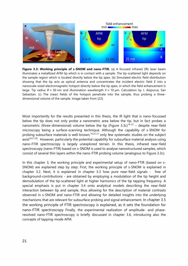
Figure 3.3: Working principle of s-SNOM and nano-FTIR. (a) A focused infrared (IR) laser beam
illuminates a metallized AFM tip which is in contact with a sample. The tip-scattered light depends on
the sample region which is located directly below the tip apex. (b) Simulated electric field distribution
showing that the tip acts as optical antenna and concentrates the incident electric field E into a
nanoscale-sized electromagnetic hotspot directly below the tip apex, in which the field enhancement is
large. Tip radius R ≈ 30 nm and illumination wavelength λ ≈ 10 µm. Calculation by J. Aizpurua, San
Sebastian. (c) The (near) fields of the hotspot penetrate into the sample, thus probing a three-
dimensional volume of the sample. Image taken from [22].
Most importantly for the results presented in this thesis, the IR light that is nano-focussed
below the tip does not only probe a nanometric area below the tip, but in fact probes a
nanometric (three-dimensional) volume below the tip (Figure 3.3c)19–22 – despite near-field
microscopy being a surface-scanning technique. Although the capability of s-SNOM for
probing subsurface materials is well-known,19,23–27 only few systematic studies on the subject
exist20,21,28. However, particularly the potential capability for subsurface material analysis using
nano-FTIR spectroscopy is largely unexplored terrain. In this thesis, infrared near-field
spectroscopy (nano-FTIR) based on s-SNOM is used to analyse nanostructured samples, which
consist of several thin layers within the nano-FTIR probing volume (analogous to Figure 3.3c).
In this chapter 3, the working principle and experimental setup of nano-FTIR (based on s-
SNOM) are explained step by step: First, the working principle of s-SNOM is explained in
chapter 3.2. Next, it is explained in chapter 3.3 how pure near-field signals - free of
background-contributions - are obtained by employing a modulation of the tip height and
demodulation of the tip-scattered light at higher harmonics of the tip tapping frequency. A
special emphasis is put in chapter 3.4 onto analytical models describing the near-field
interaction between tip and sample, thus allowing for the description of material contrasts
observed in s-SNOM and nano-FTIR and allowing for detailed insights into the underlying
mechanisms that are relevant for subsurface probing and signal enhancement. In chapter 3.5
the working principle of FTIR spectroscopy is explained, as it sets the foundation for
nano-FTIR spectroscopy Finally, the experimental realization of amplitude- and phase-
resolved nano-FTIR spectroscopy is briefly discussed in chapter 3.6, introducing also the
concepts of tapping-mode AFM.

22
3.2 Working principle of s-SNOM and nano-FTIR
s-SNOM is based on illumination of an AFM tip in proximity to a sample, and detection of the
tip-scattered light - the latter being modified by the near-field interaction between the tip and
sample. The s-SNOM probing process is sketched in Figure 3.4. The metallized AFM tip in close
vicinity to a sample is illuminated directly by an electric field E0 and indirectly by an electric
field rE0, yielding a total illuminating field Ein = (1+r)E0, where r is the sample’s Fresnel reflection
coefficient for an angle of incidence Θ (measured from the normal to the sample surface).
Figure 3.4: s-SNOM and nano-FTIR probing process. An AFM tip in close vicinity to a sample is
illuminated by the incident electric field Ein, which consists of a direct beam (left arrow labelled as “1”)
and an indirect beam (left arrow labelled as “r”) that is reflected from the sample surface with reflection
coefficient r. The illumination induces an effective electric dipole p in the tip, that depends on the tip
polarizability and the near-field interaction between the tip and sample (illustrated by curved arrows).
The intensity of the tip-scattered electric field Escat is detected directly (right arrow labelled as “1”) and
indirectly (right arrow labelled as “r”) after reflection from the sample surface, yielding the nano-FTIR
amplitude s and phase φ.
The coupled tip-sample system has an effective polarizability αeff and thus an electric dipole
p = αeff⋅Ein is induced in the tip. The dipole p scatters light directly and via reflection at the
sample surface into the far field, yielding the total scattered field Escat ∝ (1+r)p. Finally, the
ratio Escat/Ein between scattered and incident field is determined using an interferometric
detection scheme (explained below), yielding the complex-valued scattering coefficient, σ ∝
Escat/Ein, which relates to the s-SNOM and nano-FTIR amplitude s and phase φ according
to4,47,48
σ = seiφ ∝ (1+r)2 αeff. (3.1)
Specifically,
s = Abs[ (1+r)2 αeff ], (3.2)
φ = Arg[ (1+r)2 αeff ]. (3.3)

23
It is interesting to note that Equations (3.2) and (3.3) can be separated into a near-field
contribution αeff and a far-field contribution (1+r)², and thus nano-FTIR signals contain a far-
field contribution coming from a diffraction limited area of the sample. The far-field
contribution can lead to undesired effects such as peak shifts in nano-FTIR spectra (chapter 5)
but on the other hand can also be exploited e.g. to enhance the sensitivity in nano-FTIR
experiments (chapter 4). It is often overlooked that the far-field contribution is always present
in experimental nano-FTIR spectra, even if all background-scattering is perfectly suppressed
(as explained in the following).
3.3 Separation of near-field and background-scattering
In nano-FTIR experiments based on s-SNOM, the scattered light that is detected contains a tip-
scattered near-field contribution, σNF, and a background contribution, σBG, the latter
originating for example from the tip shaft or a diffraction-limited area of the sample. In order
to suppress the unwanted background-scattering, and thus to obtain the pure near-field
response of a sample, nano-FTIR experiments employ tip modulation and higher harmonic
signal demodulation.12,13 The procedure is briefly explained in Figure 3.5. The probing tip is
oscillating vertically at a frequency Ω with typical oscillation amplitudes A of a few 10 nm
(Figure 3.5a,c), yielding the tip-sample separation distance
H(t) = H0 + A(1+ cos Ωt). (3.4)
Due to the exponential decay of near-fields, the tip experiences strong near-fields at the
sample surface and almost no near-fields at large tip-sample distances (red curve in Figure
3.5b).10 On the other hand, the intensity of background light varies on the scale of the
wavelength λ (in the mid-IR spectral range λIR ≈ 5 - 10 µm), yielding an almost linear intensity
variation on the scale of the tip tapping amplitude (blue curve in Figure 3.5b).12 As a result of
such linearity, the background scattering σBG follows the harmonic sinusoidal motion of the tip
in time (blue curve in Figure 3.5d). In contrast, the near-field scattering σNF is modulated
anharmonically (red curve in Figure 3.5d). This is more clearly seen by expressing the total
scattering coefficient σ as a Fourier series,
σ = σNF + σBG = ∑ [σNF,n + σBG,n]einΩt,
∞
n=-∞ (3.5)
and plotting the n-th order Fourier components σNF,n and σBG,n of the near-field and
background contributions to the tip-scattered light (Figure 3.5e, showing absolute values).
Evidently, the background scattering σBG,n (blue) is strongly suppressed at frequencies nΩ with
n > 1. In contrast, the near-field scattering σNF,n (red) still contributes to frequencies nΩ with
n ≥ 2.2,12,13
Thus, background-free near-field signals are obtained by measuring the tip-scattered light σ
at higher harmonic frequencies nΩ of the tip-oscillation frequency Ω, yielding the demodulated
scattering coefficient σn. Experimentally, the intensity of the tip-scattered light is measured
24
interferometrically as a function of time, and a digital lock-in amplifier isolates the signals at
frequencies nΩ, directly yielding the demodulated nano-FTIR signal σn. The demodulation
order n is chosen as a trade-off between sufficient background suppression and signal-to-
noise ratio (as seen in Figure 3.5e, the near-field scattering is suppressed for very large n, but
the overall signal strength decreases).
Mathematically, the n-th order demodulated signal σn is obtained by calculating the tip-
scattered light σ (e.g. using the models described in the following chapter 3.4) as a function of
time t for one oscillation cycle of the tip-sample separation distance, Equation (3.4), and taking
the n-th Fourier coefficient F̂n with respect to time,
σn = F̂n[σ(H(t))] ∝∫ σ(H(t))einΩt2π/Ω
0
dt. (3.6)
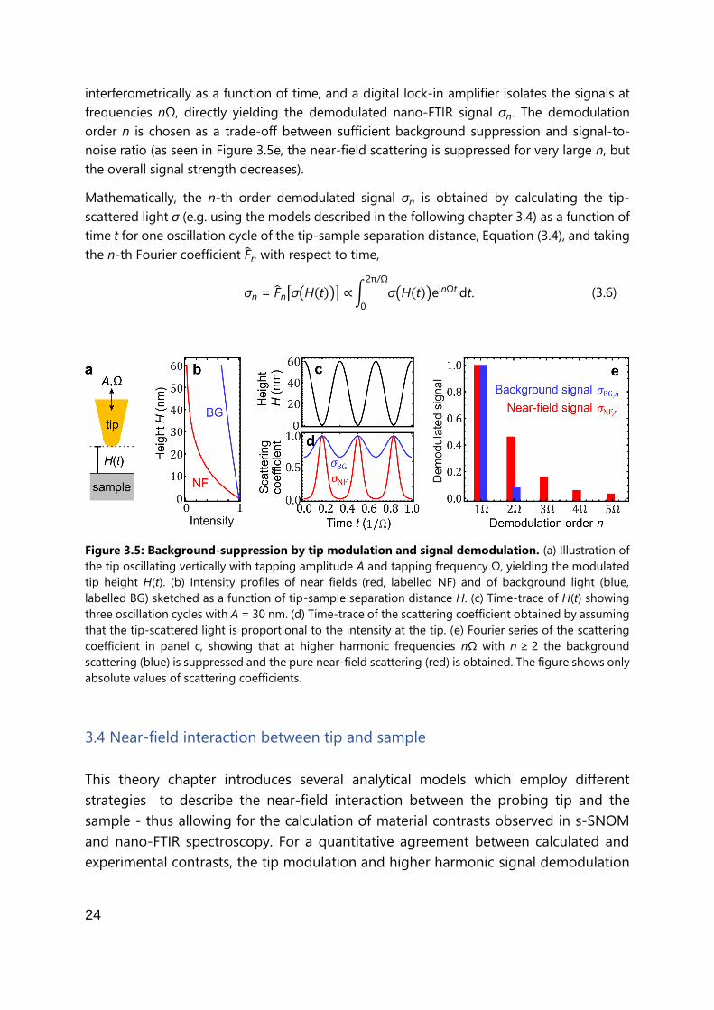
Figure 3.5: Background-suppression by tip modulation and signal demodulation. (a) Illustration of
the tip oscillating vertically with tapping amplitude A and tapping frequency Ω, yielding the modulated
tip height H(t). (b) Intensity profiles of near fields (red, labelled NF) and of background light (blue,
labelled BG) sketched as a function of tip-sample separation distance H. (c) Time-trace of H(t) showing
three oscillation cycles with A = 30 nm. (d) Time-trace of the scattering coefficient obtained by assuming
that the tip-scattered light is proportional to the intensity at the tip. (e) Fourier series of the scattering
coefficient in panel c, showing that at higher harmonic frequencies nΩ with n ≥ 2 the background
scattering (blue) is suppressed and the pure near-field scattering (red) is obtained. The figure shows only
absolute values of scattering coefficients.
3.4 Near-field interaction between tip and sample
This theory chapter introduces several analytical models which employ different
strategies to describe the near-field interaction between the probing tip and the
sample - thus allowing for the calculation of material contrasts observed in s-SNOM
and nano-FTIR spectroscopy. For a quantitative agreement between calculated and
experimental contrasts, the tip modulation and higher harmonic signal demodulation

25
described in chapter 3.3 has to be accounted for. For simplicity, the far-field
contribution (1+r)2 to the tip-scattered light is neglected throughout this chapter.
The point dipole model (PDM, chapter 3.4.1) is the simplest nano-FTIR model that
yields a qualitative agreement between calculated and experimental nano-FTIR spectra.
Despite its simplicity, the PDM has successfully been used to describe the near-field
response of for example polymers49, metals49 and semiconductors2. Importantly and
most relevant for this thesis, the PDM has also been used to predict resonant coupling
between the nano-FTIR tip and polar substrates (such as SiC or SiO2).39,50 The
phenomenon – named localized surface phonon-polariton resonance – yields greatly
enhanced near fields at the tip apex, which theoretically can be exploited to enhance
sensing of thin molecular layers51 and which is experimentally demonstrated for the
first time in chapter 4.
The finite dipole model13,48 (FDM, chapter 3.4.3) better describes the near-field
distribution around the tip apex, which results in a greater quantitative agreement
between calculated and experimental nano-FTIR spectra. For instance, the FDM has
successfully been used to quantitatively determine the local infrared absorption52,
dielectric function52 or carrier concentration27,53 from nano-FTIR spectra. The extension
of the FDM to layered samples54 (chapter 3.4.4) is used in chapter 4 to verify the
substrate-enhanced sensing of a thin organic layer on a phonon polariton-resonant
substrate.
The PDM and FDM for layered samples both introduce a so-called coupling weight
function (CWF), that describes the distribution of in-plane momenta q = √kx2 + ky
2 of
the reflected near fields that are provided and probed by the nano-FTIR tip. The
concept of momentum-dependent probing (described by the momentum-dependent
Fresnel reflection coefficient) is highly important for the correct interpretation of nano-
FTIR spectra, particularly for layered samples, as discussed in chapter 3.4.5 and
investigated in chapter 5.
Note that the presented models describe nano-FTIR contrasts caused by different
material properties (such as changes in the sample permittivity) and that the models
are not suitable to describe contrasts caused by additional electric fields at the sample
surface (such as the ones produced by propagating surface polaritons). For the latter,
the reader is referred to corresponding literature55,56.

26
3.4.1 Point dipole model for bulk samples
The point dipole model (PDM) is illustrated in Figure 3.6a. The nano-FTIR tip is modelled as a
spherical particle in air, with radius R, permittivity ϵt and polarizability
αt = 4πϵ0R3(ϵt-1)/(ϵt+2), (3.7)
located at a height H above the sample surface. The incident field Ein induces the total electric
point dipole p = p0 + p
1 in the tip, where p
0 = αtEin is the primary dipole that is induced by
the illuminating field and p1 = αtG⋅p is induced by the near-field interaction between tip and
sample. G needs to be determined, such that the product G⋅p describes the electric field that
is produced by the dipole p, reflected at the sample surface and then acts back onto the dipole
p itself. The self-consistent solution
p = αt
1-αtG⋅Ein ≡ αeff⋅Ein (3.8)
defines the effective polarizability αeff of the coupled tip-sample system, which relates to nano-
FTIR amplitude s and phase φ signals via seiφ ∝ αeff, Equations (3.1) - (3.3).
To determine the effective polarizability αeff which describes the near-field interaction between
tip and sample, an expression for G in Equation (3.8) needs to be found. In the PDM, G is
obtained from a simple electrostatic dipole-dipole interaction. By using the method of image
charges57, the near field distribution that is produced by the dipole p and reflected at the
sample surface is given at the position r = (x,y,z) by 57
Erefl(r) = 1
4πϵ0
3n(p'⋅n') - p'
|r - r'|3
, (3.9)
where r' = (0,0,-H-R) is the position of the image dipole p' = ±βp, the unit vector n is directed
from r' to r and β = (ϵ-1)/(ϵ+1) is the electrostatic reflection coefficient of a sample with
permittivity ϵ. The sign of p' = ±βp depends on the orientation of p, as illustrated in Figure
3.6b. A vertical orientation of p induces the image dipole p' = +βp in the sample and a
horizontal orientation of p induces the image dipole p' = -βp in the sample.10 When p is
oriented vertically (p ∥ z), the reflected field at the position of p itself (i.e. at the centre of the
sphere drawn in Figure 3.6a) is given by
Erefl(0,0,H+R) = 1
16πϵ0
βp
(H+R)3 ≡ Gzp (3.10)
from which we identify Gz, which carries the index z to show that p is oriented vertically. By
plugging Gz into Equation (3.8) we obtain
αeff
z = αt
1-αtβ
16πϵ0(H+R)3
. (3.11)

27
Analogously, when p is oriented horizontally (p ⊥ z), we obtain
Erefl(0,0,H+R) = 1
32πϵ0
βp
(H+R)3 ≡ Gxp (3.12)
and
αeff
x = αt
1-αtβ
32πϵ0(H+R)3
. (3.13)
Figure 3.6: Point dipole model for semi-infinite samples. (a) The nano-FTIR tip is modelled by a
spherical particle of radius R at a height H above a sample with permittivity ϵ and electrostatic reflection
coefficient β = (ϵ-1)/(ϵ+1). The illuminating electric field Ein induces a point dipole p at the sphere center,
which interacts with its image dipole p' induced in the sample (illustrated by curved arrows). The self-
interacting dipole p produces the electric field Escat, which is detected in the far field. The model accounts
for far-field illumination and detection of the tip-scattered field via reflection at the sample surface, with
Fresnel reflection coefficient r (indicated by red straight arrows). (b) Image dipole p' = ±βp illustrated
for vertically oriented dipoles (upper panel) and horizontally oriented dipoles (lower panel).
Using Equations (3.11) and (3.13), we simulate the nano-FTIR amplitude s3 on a gold sample
for a vertically oriented dipole (solid curve in Figure 3.7) and a horizontally oriented dipole
(dashed curve in Figure 3.7) as a function of tip-sample distance H. The calculation includes the
tip height modulation and higher harmonic signal demodulation (here tip tapping amplitude
A = 30 nm and demodulation order n = 3) by calculating αeffz and αeff
x for one oscillation cycle
of H(t) and taking the nth-order Fourier coefficient F̂n with respect to time, as explained above
(Equations (3.4) and (3.6)). Both curves show that s3 quickly decays as the tip-sample distance
increases, which is typical of near field interaction between the nano-FTIR tip and the sample.10
We further find for small tip-sample distances, that the nano-FTIR amplitude is larger when the
dipole is oriented vertically, compared to a horizontally oriented dipole. A vertical orientation
of the tip- and sample-dipoles leads to increased tip-sample interaction and thus an increased

28
effective polarizability of the tip. This increased tip-polarizability along the z-direction is further
enhanced in nano-FTIR experiments by using probing tips with an elongated structure (with
nm-sized tip apex radius and µm-sized tip shaft length). Therefore, αeffx is typically and in the
following neglected and only αeffz is considered relevant to describe nano-FTIR amplitude and
phase signals.
Figure 3.7: Approach curve calculated by PDM. Nano-FTIR amplitude s3 as a function of tip-sample
distance H, calculated for a vertically oriented dipole (solid curve) and a horizontally oriented dipole
(dashed curve). Calculated for a gold tip and gold sample with permittivity ϵs = -5000+i1000, tip radius
R = 30 nm, tip tapping amplitude A = 30 nm and demodulation order n = 3.
3.4.2 Point dipole model for layered samples
The PDM for layered samples51 is illustrated in Figure 3.8a. As before, the tip is modelled as a
sphere with polarizability αt and radius R which is located at a height H above the sample
surface. The sample consists of an arbitrary number of horizontally stacked layers and each
layer i has a thickness di, permittivity ϵi and permeability μi. For simplicity, we assume that all
materials are isotropic and non-magnetic, i.e. ϵi is a scalar and μi = 1. The bottom-most layer
(in the figure labelled with “ϵ4”) is semi-infinite. As explained above, illumination of the tip-
sample system with the electric field Ein induces the electric dipole
p = αtEin + αtG⋅p (3.14)
in the sphere centre. To express the near-field induced dipole p1 = αtG⋅p, Aizpurua et al. used
the Green’s function of a dipole located at height z0 = R+H above the sample surface.10,51
In the following, G(r0,r0) corresponds to the reflection term in the Green’s function of an
arbitrarily oriented dipole p located at r0 = (0,0,z0), and the Green’s function is taken at the
position r0 of the dipole itself (see Appendix 6.2):

29
G(r0,r0) = iω2μ
0
8π2∫ [Mrefl
s+Mrefl
p]qei2kz1z0 dq
∞
0
,
(3.15)
Mrefls
= πrs(q)
kz1
[1 0 00 1 0
0 0 0
] , (3.16)
Mreflp
= -πrp(q)
k12
[
kz1 0 0
0 kz1 0
0 0 -2q2/kz1
] ,
(3.17)
where ω = ck is the angular frequency of the incident light in vacuum, the waves in medium i
carry the total momentum ki = ω
c√ϵi , out-of-plane momentum kzi = √ki
2-q2 and in-plane
momentum q = √kx2+ky
2, and rs(q) respectively rp(q) are the reflection coefficients of the entire
sample for s- and p-polarized light as a function of q. As an example, rp(q) for one layer on a
substrate is given by18
rp = r12+r23ei2kz2d2
1+r12r23ei2kz2d2 , (3.18)
with the single-interface Fresnel reflection coefficients rij = (ϵjkzi - ϵikzj)/(ϵjkzi + ϵikzj) and the
layer thickness d2. Multiple layers on a substrate can be described by recursively using Equation
(3.18) as expression for r23 or using the transfer matrix method32.
The integral in Equation (3.15) can be interpreted as a superposition of plane waves with in-
plane momenta q, which are produced by the dipole p and reflected at the sample surface. This
so-called angular spectrum representation10 is highly suited for the description of layered
samples, because the in-plane momentum q is conserved across all material boundaries10.
Figure 3.8b illustrates the momentum q in the sample plane (xy-plane) for a propagating wave
(red arrow, q ≤ k1) and an evanescent wave (blue arrow, q > k1). For propagating waves, the
in-plane momentum q = ki sin θi is determined by the angle of incidence θi with respect to the
surface normal (Figure 3.8c). For evanescent waves, the large in-plane momentum q > ki leads
to a fast decay of the electric fields along the z direction, which is determined by momentum
conservation kzi = √ki2-q2 and which is illustrated in Figure 3.8d.
Equations (3.15) - (3.17) are greatly simplified by assuming a vertically oriented dipole
p = (0,0,pz). In this case, only the single matrix element Gzz contributes to Equation (3.14) and
thus the effective tip polarizability in z-direction is given by

30
αeffz =
αt
1-αtGzz
,
Gzz = iω2μ
0
4πk12
∫ rp(q)q3
kz1
ei2kz1z0 dq,∞
0
(3.19)
(3.20)
which in combination with Equation (3.1) describe nano-FTIR amplitude and phase spectra of
samples made of an arbitrary number of isotropic layers.
Importantly and in contrast to the PDM for bulk samples, the sample response is described in
Equation (3.20) by the electrodynamic reflection coefficient rp(q), which for each q is weighted
with the factor
wPDM(q) = (q3/kz1)ei2kz1z0, (3.21)
that describes which momenta are provided and probed by the tip. This so-called coupling
weight function (CWF) wPDM(q) is highly important for the correct description of nano-FTIR
signals51,54,58,59 and is discussed in more detail in chapter 3.4.5.
Figure 3.8: Point dipole model for layered samples. (a) The nano-FTIR tip is modelled by a spherical
particle of radius R at a distance H above a layered sample. Each layer i has a permittivity ϵi, thickness di
and single-interface Fresnel reflection coefficient rij(q) with respect to the underlying layer j. The
illuminating light with wavevector k1 and electric field vector Ein induces a point dipole p at the sphere
center, which interacts with the sample. (b) The in-plane momentum q = √kx2+ky
2 is illustrated for a
propagating wave (red arrow, q ≤ k1) and an evanescent wave (blue arrow, q > k) in comparison with the
momentum k1 of the incident light in air. (c,d) Illustrations showing the relation between (c) in-plane
momentum q and incidence angle θ1 (for propagating waves in air) and (d) in-plane momentum q and
exponential decay length ikz (for evanescent waves).

31
3.4.3 Finite dipole model for bulk samples
The finite dipole model13,48 (FDM) is illustrated in Figure 3.9. The nano-FTIR tip is modelled as
a perfectly conducting prolate spheroid in air, with apex radius R and major half-axis length L,
located at a height H above the sample surface. Analytical calculations show that such spheroid
produces (under external illumination) a near-field distribution that closely matches that of a
point charge, rather than that of a point dipole or extended dipole.48 Therefore, and in contrast
to the PDM, the dipole induced in the tip is spatially extended. The primary dipole p0 ≈ 2LQ0
(blue arrow in Figure 3.9) that is induced by the illuminating field Ein consists of the point
charges ±Q0 which are located at distances W0 = 1.31RL
L+2R from the spheroid apexes. Due to the
large distance of the upper point charge (-Q0) to the sample surface, it is considered to not
contribute to the near-field interaction between tip and sample.
Figure 3.9. Finite dipole model for semi-infinite samples. The nano-FTIR tip is modelled by a prolate
spheroid of length 2L and apex radius R at a distance H above a sample with permittivity ϵ and
electrostatic reflection coefficient β = (ϵ-1)/(ϵ+1). The illuminating electric field Ein induces an extended
dipole p0 (blue arrow) in the tip, constituted by the point charges ±Q0 which are located at distances W0
from the tip apexes. The point charge Q0 creates an image charge Q0' in the sample, which yields an
additional near-field induced dipole p1 (green arrow) in the tip. The dipole p1 consists of the point
charges Q1 at a distance W1 from the sample-near tip apex and -Q1 in the spheroid center. The model
accounts for far-field illumination and detection of the tip-scattered field Escat via reflection at the sample
surface, with Fresnel reflection coefficient r (indicated by red arrows).
In the FDM, the near-field interaction between tip and sample is described by the charge +Q0,
which induces an image charge Q0’ = -βQ0 in the sample, with β = (ϵ-1)/(ϵ+1) being the quasi-
electrostatic Fresnel reflection coefficient for a semi-infinite sample with permittivity ϵ. The
distance z0 = R+H of Q0’ to the sample surface is the same as the height of Q0 above the
sample, z0 (method of image charges57). The image charge Q0’ acts back on the tip by inducing
a line charge distribution in the tip, which is approximated by a point charge Q1 = βQ0f0 at a
32
distance W1 = R/2 from the tip apex and its counter charge -Q1 at the spheroid center, which
together form the dipole p1 ≈ LQ1 (green arrow in Figure 3.9). Self-consistent treatment of the
problem yields13
Q1 = βQ0f0 + βQ1f1, (3.22)
where fi are geometry factors depending on the tip apex radius R, spheroid major half-axis
length L and tip-sample distance H, and given by
fi = (g-R+2H+Wi
2L) ⋅
ln (4L
R+4H+2Wi)
ln (4LR
) (3.23)
with I = {1, 2}. The g-factor is a model parameter that describes the amount of the induced line
charge that is still relevant for the near-field interaction. It is empirically found to be
g ≈ 0.7±0.1.48 By expressing the total induced dipole moment p = p0 + p
1 = αeffEin using
Equation (3.22), it can be shown that
αeff ∝ 1 + 1
2⋅
βf01-βf1
, (3.24)
which in combination with Equation (3.1) describes nano-FTIR amplitude and phase spectra.
The proportionality is sufficient when only relative material contrasts are considered, i.e., a
reference material is used to normalize nano-FTIR spectra.
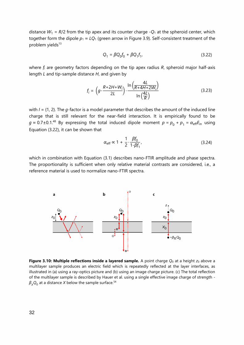
Figure 3.10: Multiple reflections inside a layered sample. A point charge Q0 at a height z0 above a
multilayer sample produces an electric field which is repeatedly reflected at the layer interfaces, as
illustrated in (a) using a ray-optics picture and (b) using an image charge picture. (c) The total reflection
of the multilayer sample is described by Hauer et al. using a single effective image charge of strength -
βXQ0 at a distance X below the sample surface.54
33
3.4.4 Finite dipole model for layered samples
The FDM in Equation (3.24) is valid only for semi-infinite samples, in which the sample response
to a point charge is described with a single image charge. In layered samples, however, multiple
reflections between the sample interfaces take place (Figure 3.10a), which can be described by
a series of image charges (Figure 3.10b).60 In order to extend the FDM to layered samples,
Hauer et al. replaced the infinite series of image charges by one effective image charge (Figure
3.10c), for which the location X and strength βX are calculated numerically.54 To this end, Hauer
et al. used the reflected electrostatic potential Φ (which is produced by a charge Q0 at height
z0 and reflected at the surface of a multilayer sample) which along the tip-axis (z-axis) is given
by61
Φ(z)= ∫ β(q)e-2qz0-qz∞
0
dq, (3.25)
where q is the in-plane momentum of light and β(q) is the quasi-electrostatic reflection
coefficient of the multilayer sample. As an example, β(q) for one layer of thickness d on a
substrate is given by
β(q) = β
12+β
23e-2qd
1+β12
β23
e-2qd . (3.26)
By the method of image charges, the reflected electrostatic potential Φ is equivalent to that of
a point charge below the sample surface (the effective image charge). By applying the boundary
conditions of the electric potential and its derivative along the surface normal Φ' = (∂Φ/∂z), the
following expressions for the effective charge strength βX and effective position X are
obtained:54
βX = -
Φ2
Φ'|z=0 and X =
Φ
Φ'|z=0 – z0. (3.27)
Finally, Equation (3.27) is used in modified versions of Equations (3.23) and (3.24),54
fi,X = (g – R+H+Xi
2L) ⋅
ln (4L
R+2H+2Xi)
ln (4LR
), (3.28)
and
αeff ∝ 1+1
2⋅
βXf0,X
1 – βXf1,X
, (3.29)
which in combination with Equation (3.1) describe nano-FTIR amplitude and phase spectra.
From a computational standpoint, it can be beneficial to introduce the dimensionless variable
ξ = q⋅z0 in Equation (3.25), which yields the practical expression for the electrostatic potential

34
Φ = 1
z0
∫ β (ξ
z0
)e-ξ(2z0+z)/z0
∞
0
dξ. (3.30)
Note that the sample response is described in Equations (3.25) and (3.30) by the quasi-
electrostatic reflection coefficient β(q), which for each q is weighted with a weight function
similar to Equation (3.21) of the PDM for multilayer samples. Specifically, the CWF of the FDM
is obtained from the expression for the electric field Ez = -∂Φ(z)/∂z and given by62
wFDM = qe-2qz0 (3.31)
In the following, the role of a CWF in nano-FTIR spectroscopy is briefly discussed, as it will be
used extensively in the results chapter 5. For simplicity, only wPDM is discussed and similar results
are expected for wFDM.
3.4.5 Momentum-dependent probing of the Fresnel reflection coefficient
In order to understand more intuitively which sample properties are actually probed in nano
FTIR spectroscopy, this chapter briefly discusses the relation between the sample permittivity
ϵs, the sample’s Fresnel reflection coefficient rp(ν,q) and the coupling weight function (CWF)
wPDM(q) = (q3/kz1)ei2kz1z0 of nano-FTIR (Equation (3.21)), followed by a brief comparison with
far-field FTIR and total internal reflection (TIR) FTIR. To this end, we consider a layer of a
hypothetical material which features a charge-carrier response and a molecular vibration in the
mid-IR spectral range. The permittivity ϵs is described using the Drude-Lorentz model via63
ϵs(ν) = ϵ∞ (1 – νp
2
ν2+iνγp
) + AL
2
νL2 – ν2 + iνγ
L
, (3.32)
with the high-frequency permittivity ϵ∞, plasma frequency νp, electronic damping rate γp,
Lorentz oscillator strength AL, frequency νL and damping rate γL (Figure 3.11a). Calculated
nano-FTIR spectra for a layer thickness d = 200 nm (solid lines) and d = 20 nm (dashed lines)
are shown in Figure 3.11b. Each amplitude spectrum (black curves) shows two spectral features
with a dispersive line shape and each phase spectrum (red curves) shows two spectral peaks
around νp and νL, caused by collective electron excitation and excitation of the molecular
vibration respectively. Despite their similar appearance in nano-FTIR spectra, the contrasts (i.e.
peak heights) differ in their relation to the sample permittivity. For weak oscillators (Re ϵ > 0,
including molecular vibrations of organic materials) the nano-FTIR amplitude and phase follow
approximately the real and imaginary parts of the permittivity49. In contrast, for strong
oscillators (Re ϵ < 0, including plasmons or phonons), the nano-FTIR amplitude is resonantly
enhanced around ϵ ≈ -2 (Ref. 50), owing to a resonant coupling between tip and sample, as
further explained and exploited in chapter 4. Importantly, Figure 3.11b shows that nano-FTIR
spectra are not entirely defined by the sample permittivity, but also depend on the sample
geometry. Specifically, the nano-FTIR amplitude spectra show that the spectral peak position

35
associated with charge carrier excitations is strongly shifted as a function of the layer thickness
d. In chapter 5 it is thoroughly investigated how nano-FTIR spectra of an organic layer featuring
a molecular vibration are modified as function of the sample geometry (i.e. varying thickness
or depth of the organic layer).
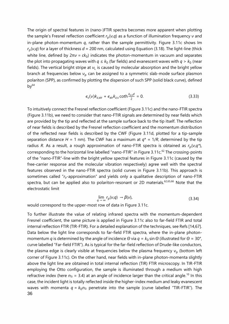
Figure 3.11: Relation between nano-FTIR spectra, the coupling weight function and momentum-
dependent Fresnel reflection coefficient. (a) Real and imaginary parts of the permittivity ϵs for a
hypothetical material described by a Drude-Lorentz model with ϵ∞ = 5, νp = 1000 cm-1, γp = 250 cm-1,
AL = 500 cm-1, frequency νL = 1750 cm-1 and damping rate γL = 50 cm-1. (b) Corresponding nano-FTIR
spectra of a d = 200 nm-thick layer (solid curves) and d = 20 nm-thick layer (dashed curves) in air,
calculated using the PDM for layered samples for a tip radius R = 50 nm, tapping amplitude A = 25 nm
and demodulation order n = 3. (c) Imaginary part of the Fresnel reflection coefficient rp(ν,q) of the 200
nm-thick layer sample, as a function of frequency ν and in-plane momentum q. Vertical lines indicate νp
(solid) and νL (dashed). The solid black curve indicates the dispersion of symmetric slab-mode SPPs in a
layer of thickness d = 200 nm. White curves indicate the dispersion of free-space photons (“Light line”)
and the momenta probed by nano-FTIR, TIR-FTIR (nSi = 3.4) and far-field FTIR spectroscopy (Θ = 30°).
(d) Coupling weight function of the PDM, wPDM(q), for a tip-sample separation distance H = 1 nm. The
horizontal line indicates q* = 1/R.
36
The origin of spectral features in (nano-)FTIR spectra becomes more apparent when plotting
the sample’s Fresnel reflection coefficient rp(ν,q) as a function of illumination frequency ν and
in-plane photon-momentum q, rather than the sample permittivity. Figure 3.11c shows Im
rp(ν,q) for a layer of thickness d = 200 nm, calculated using Equation (3.18). The light-line (thick
white line, defined by 2πν = ck0) indicates the photon-momentum in vacuum and separates
the plot into propagating waves with q ≤ k0 (far fields) and evanescent waves with q > k0 (near
fields). The vertical bright stripe at νL is caused by molecular absorption and the bright yellow
branch at frequencies below νp can be assigned to a symmetric slab-mode surface plasmon
polariton (SPP), as confirmed by plotting the dispersion of such SPP (solid black curve), defined
by64
ϵs(ν)kz,air + ϵairkz,s cothkz,sd
2 = 0. (3.33)
To intuitively connect the Fresnel reflection coefficient (Figure 3.11c) and the nano-FTIR spectra
(Figure 3.11b), we need to consider that nano-FTIR signals are determined by near fields which
are provided by the tip and reflected at the sample surface back to the tip itself. The reflection
of near fields is described by the Fresnel reflection coefficient and the momentum distribution
of the reflected near fields is described by the CWF (Figure 3.11d, plotted for a tip-sample
separation distance H = 1 nm). The CWF has a maximum at q* = 1/R, determined by the tip
radius R. As a result, a rough approximation of nano-FTIR spectra is obtained as rp(ν,q*),
corresponding to the horizontal line labelled “nano-FTIR” in Figure 3.11c.62 The crossing-points
of the “nano-FTIR”-line with the bright yellow spectral features in Figure 3.11c (caused by the
free-carrier response and the molecular vibration respectively) agree well with the spectral
features observed in the nano-FTIR spectra (solid curves in Figure 3.11b). This approach is
sometimes called “rp-approximation” and yields only a qualitative description of nano-FTIR
spectra, but can be applied also to polariton-resonant or 2D materials.62,65,66 Note that the
electrostatic limit
limq → ∞
rp(ν,q) → β(ν), (3.34)
would correspond to the upper-most row of data in Figure 3.11c.
To further illustrate the value of relating infrared spectra with the momentum-dependent
Fresnel coefficient, the same picture is applied in Figure 3.11c also to far-field FTIR and total
internal reflection FTIR (TIR-FTIR). For a detailed explanation of the techniques, see Refs [14,67].
Data below the light line corresponds to far-field FTIR spectra, where the in-plane photon-
momentum q is determined by the angle of incidence Θ via q = k0 sin Θ (illustrated for Θ = 30°,
curve labelled “Far-field FTIR”). As is typical for the far-field reflection of Drude-like conductors,
the plasma edge is clearly visible at frequencies below the plasma frequency νp (bottom left
corner of Figure 3.11c). On the other hand, near fields with in-plane photon-momenta slightly
above the light line are obtained in total internal reflection (TIR) FTIR microscopy. In TIR-FTIR
employing the Otto configuration, the sample is illuminated through a medium with high
refractive index (here nSi = 3.4) at an angle of incidence larger than the critical angle.10 In this
case, the incident light is totally reflected inside the higher-index medium and leaky evanescent
waves with momenta q = k0nSi penetrate into the sample (curve labelled “TIR-FTIR”). The

37
crossing-point of the “TIR-FTIR”-line with the SPP dispersion (black curve) indicates that SPPs
can be excited and probed – as routinely exploited for example in molecular sensors based on
SPP resonances68. Importantly, the optical properties of the sample are entirely contained in
the Fresnel reflection coefficient and different FTIR techniques (including nano-FTIR) merely
probe different parts (different momenta) of the same reflection coefficient. To briefly recap,
the main message of Figure 3.11 and the above discussion is that in nano-FTIR, the reflection
coefficient rp(ν,q) is probed at momenta around q* = 1/R,62,65,66 which will be further exploited
in chapter 5 to explain spectral peak shifts in nano-FTIR spectra of thin organic surface and
subsurface layers.
At this point it must be noted that the CWF is still poorly understood and its relation to the
sample’s Fresnel reflection coefficient yield only a strongly simplified description of nano-FTIR
spectroscopy, and that important aspects such as the tip modulation and signal demodulation
are completely neglected. This paragraph is meant to give a small overview on variations of
the CWF found in literature and to highlight some of the existing problems related to the CWF.
Firstly, note that for nano-FTIR spectroscopy a single value of q is insufficient to properly
describe observations in nano-FTIR experiments, as the entire CWF (Figure 3.12a) must be
considered. For example, the high lateral spatial resolution in s-SNOM and nano-FTIR is
explained by probing strongly confined evanescent waves with high momenta q ~ 1/R, whereas
the vertical probing depth in s-SNOM is much larger, indicating that (also) longer-reaching
evanescent waves with smaller momenta q ~ 0.1/R are probed.24,54,69 This point is further
discussed in chapter 5.
Figure 3.12: Variations of the coupling weight function (CWF). CWF of the PDM for layered samples.
(a) Plotted for H = 1 nm. (b) Time-averaged CWF <wPDM(q,H(t)>t over one oscillation cycle of the tip
modulation H(t) with tapping amplitude A = 25 nm. (c) Demodulated CWF for A = 25 nm and
demodulation orders n = {2, 3, 4}. (a-c) Tip radius R = 50 nm.

38
Furthermore, the peak position of the CWF depends on the tip-sample separation distance H
– larger distances H favouring lower momenta q. To account for the tip height modulation of
nano-FTIR experiments, a time-averaged CWF <w(q,H(t))>t is therefore frequently used in
literature,66,70 which effectively shifts the CWF to lower momenta (Figure 3.12b). On the other
hand, it is experimentally found that the spatial resolution actually increases, when the tip
height is modulated and the signal is demodulated20,21,71 – an effect also known as “virtual tip
sharpening”72,73 – which corresponds to a shift of the CWF to higher momenta. This apparent
contradiction between experimental observations and the time-averaged CWF shows that
further studies related to the CWF are needed, particularly to investigate the role of the tip
modulation and signal demodulation parameters.
As of date, a direct relation between higher harmonic signal demodulation and the CWF has
not yet been demonstrated. Here, a simplified “demodulated coupling weight function” is
obtained (for illustrative purposes only) by modulating the tip height and taking the n-th order
Fourier coefficients F̂n of wPDM(q,H(t)) with respect to time (analogous to Equation (3.6)). The
demodulated CWF (Figure 3.12c) describes well that the spatial resolution is increased by tip
modulation and signal demodulation, i.e. that the CWF is shifted to higher momenta compared
to the standard CWF (Figure 3.12a). Furthermore, the shift increases for higher demodulation
orders n, which is consistent with the further increased spatial resolution at larger n observed
in s-SNOM experiments. Note that Figure 3.12c should be used with care, as a more rigorous
(and by no means trivial) derivation is needed that accounts for multiple reflections of near
fields between tip and sample (i.e. account for the full nano-FTIR model such as the PDM).

39
3.5 Fourier-transform infrared spectroscopy (FTIR)
In this chapter the working principle of FTIR spectroscopy is explained, as it sets the foundation
for nano-FTIR spectroscopy. This chapter essentially follows the descriptions of Refs [14,40],
including the main data processing steps required to obtain infrared spectra from experimental
data. A typical FTIR spectrometer is based on a Michelson interferometer setup as shown in
Figure 3.13. Broadband infrared radiation of the IR light source is split by a beam splitter (BS)
into two beams A and B. The two beams are reflected in the interferometer arms and (A+B)
recombined at the detector position. Importantly, the two beams have an optical path length
difference of 2Δx, which can be adjusted by linearly translating the reference (RM) mirror along
the beam axis by a distance Δx. The interference of the beams A+B varies as a function of the
optical path length difference.
Figure 3.13: Michelson interferometer setup as used in FTIR spectroscopy. Broadband infrared
radiation is split by a beam splitter (BS) into two beams A and B, which are reflected by flat mirrors and
recombined by the BS at the detector position (A+B). Linear translation of a moving mirror by a distance
Δx introduces a phase difference between the beams A and B, thus modifying the interference of A+B
at the detector position (e.g. from constructive interference to destructive interference).
For a mathematical description of the interference, we first assume a monochromatic light
source that emits a plane wave electric field E0 = |E0|eiν0t with frequency ν0 = 1/λ0 (given in
cm-1), free-space wavelength λ0 and intensity I0∝|E0|2. The light is split by the beamsplitter into
two beams EA = |EA|eiν0t and EB = |EB|eiν0t+iφ
B which propagate along the two paths A and B
respectively, with φB = 4πν0Δx being the phase difference caused by a different length Δx of
the interferometer arms. The magnitudes of |EA| and |EB| depend on the details of the
experimental setup such as the transmission characteristics of the beamsplitter, atmospheric
absorption or the spectral sensitivity of the infrared detector. Interference of the beams A and
B at the detector position yields the intensity
I(Δx) ∝ |EA|2 + |EB|2 + 2|EA||EB| cos [4πν0Δx] , (3.35)
which oscillates as a function of the path difference Δx due to φB = 4πν0Δx. In the following,
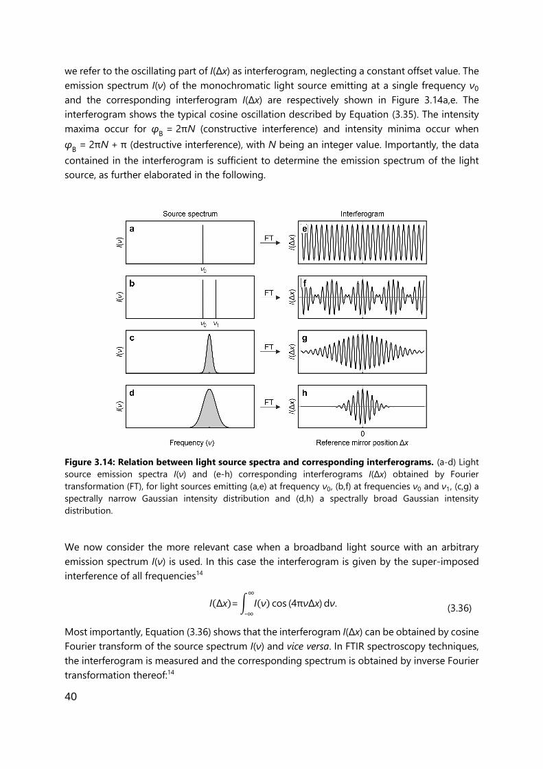
40
we refer to the oscillating part of I(Δx) as interferogram, neglecting a constant offset value. The
emission spectrum I(ν) of the monochromatic light source emitting at a single frequency ν0
and the corresponding interferogram I(Δx) are respectively shown in Figure 3.14a,e. The
interferogram shows the typical cosine oscillation described by Equation (3.35). The intensity
maxima occur for φB = 2πN (constructive interference) and intensity minima occur when
φB = 2πN + π (destructive interference), with N being an integer value. Importantly, the data
contained in the interferogram is sufficient to determine the emission spectrum of the light
source, as further elaborated in the following.
Figure 3.14: Relation between light source spectra and corresponding interferograms. (a-d) Light
source emission spectra I(ν) and (e-h) corresponding interferograms I(Δx) obtained by Fourier
transformation (FT), for light sources emitting (a,e) at frequency ν0, (b,f) at frequencies ν0 and ν1, (c,g) a
spectrally narrow Gaussian intensity distribution and (d,h) a spectrally broad Gaussian intensity
distribution.
We now consider the more relevant case when a broadband light source with an arbitrary
emission spectrum I(ν) is used. In this case the interferogram is given by the super-imposed
interference of all frequencies14
I(Δx)= ∫ I(ν) cos (4πνΔx)
∞
-∞
dν. (3.36)
Most importantly, Equation (3.36) shows that the interferogram I(Δx) can be obtained by cosine
Fourier transform of the source spectrum I(ν) and vice versa. In FTIR spectroscopy techniques,
the interferogram is measured and the corresponding spectrum is obtained by inverse Fourier
transformation thereof:14
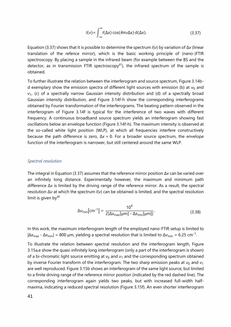
41
I(ν)= ∫ I(Δx) cos(4πνΔx)∞
-∞
d(Δx). (3.37)
Equation (3.37) shows that it is possible to determine the spectrum I(ν) by variation of Δx (linear
translation of the refence mirror), which is the basic working principle of (nano-)FTIR
spectroscopy. By placing a sample in the infrared beam (for example between the BS and the
detector, as in transmission FTIR spectroscopy67), the infrared spectrum of the sample is
obtained.
To further illustrate the relation between the interferogram and source spectrum, Figure 3.14b-
d exemplary show the emission spectra of different light sources with emission (b) at ν0 and
ν1, (c) of a spectrally narrow Gaussian intensity distribution and (d) of a spectrally broad
Gaussian intensity distribution, and Figure 3.14f-h show the corresponding interferograms
obtained by Fourier transformation of the interferograms. The beating pattern observed in the
interferogram of Figure 3.14f is typical for the interference of two waves with different
frequency. A continuous broadband source spectrum yields an interferogram showing fast
oscillations below an envelope function (Figure 3.14f-h). The maximum intensity is observed at
the so-called white light position (WLP), at which all frequencies interfere constructively
because the path difference is zero, Δx = 0. For a broader source spectrum, the envelope
function of the interferogram is narrower, but still centered around the same WLP.
Spectral resolution
The integral in Equation (3.37) assumes that the reference mirror position Δx can be varied over
an infinitely long distance. Experimentally however, the maximum and minimum path
difference Δx is limited by the driving range of the reference mirror. As a result, the spectral
resolution Δν at which the spectrum I(ν) can be obtained is limited, and the spectral resolution
limit is given by40
Δνmin[cm-1] = 10
4
2|Δxmax[µm] - Δxmin[µm]|. (3.38)
In this work, the maximum interferogram length of the employed nano-FTIR setup is limited to
|Δxmax - Δxmin| = 800 µm, yielding a spectral resolution that is limited to Δνmin = 6.25 cm-1.
To illustrate the relation between spectral resolution and the interferogram length, Figure
3.15a,e show the quasi-infinitely long interferogram (only a part of the interferogram is shown)
of a bi-chromatic light source emitting at ν0 and ν1 and the corresponding spectrum obtained
by inverse Fourier transform of the interferogram. The two sharp emission peaks at ν0 and ν1
are well reproduced. Figure 3.15b shows an interferogram of the same light source, but limited
to a finite driving range of the reference mirror position (indicated by the red dashed line). The
corresponding interferogram again yields two peaks, but with increased full-width half-
maxima, indicating a reduced spectral resolution (Figure 3.15f). An even shorter interferogram

42
(Figure 3.15c) yields a spectrum, in which only one broad peak can be observed (Figure 3.15g).
Clearly, the spectral resolution has decreased such that the frequencies ν0 and ν1 are not
resolved anymore. Note that the fast oscillations observed in the spectra (panels f, g) are an
artifact caused by the sudden stop of the interferogram at the maximum and minimum
positions of Δx. As shown in Figure 3.15d,h, the inverse Fourier transformation of the boxcar
functions produces a spectrum that shows the same fast oscillatory behavior, which is not
related to the light source but can be considered as part of the instrument response function.
The oscillations can partially be removed at the cost of a slightly reduced spectral resolution,
as explained below in the following.
Figure 3.15: Spectral resolution as a function of interferogram length. (a-c) Interferograms
of different length and (e-g) corresponding spectra obtained by inverse Fourier transformation
(FT-1). In all cases, the same bi-chromatic light source emitting at frequencies ν0 and ν1 is
assumed. (d) Boxcar functions that describe the finite interferogram lengths that are used in
panels b and c and (h) the corresponding spectra.
Apodization
As shown above and for convenience repeated in Figure 3.16a,e the sudden ending of an
interferogram leads to an artifact which is observed as satellite oscillations on both sides of the
main peaks. By multiplying the interferogram with a smooth function – the so-called
apodization function or window function – the sudden ending of the interferogram is
smoothed out, which effectively suppresses the fast oscillations in the spectrum (Figure 3.16b-
h). The interferogram in Figure 3.16b is obtained by multiplying the original interferogram with
a Blackman-Harris 3-term function14 (blue dashed line) and the corresponding spectrum

43
(Figure 3.16f) is essentially artifact-free. However, the spectral resolution is decreased, because
the interferogram is effectively shortened by the apodization function. In general, a trade-off
between artifact-suppression and spectral resolution must be made. The nano-FTIR spectra
shown in this thesis are obtained using a modified Blackman-Harris 3-term function (green
dashed curve in Figure 3.16c). In this case, only the datapoints near the interferogram edges
are modified, leaving most data points near the WLP unmodified. The resulting spectrum is
mostly artifact-free, while maintaining a high spectral resolution (Figure 3.16g). The effect of
the apodization function on the resulting spectrum can be visualized by directly plotting the
inverse Fourier transformation of the apodization function (Figure 3.16h), which will be
convoluted with the original spectrum.
Figure 3.16: Varying apodizations of the same interferogram. (a-c) The same interferogram is
multiplied by various apodization functions (dashed lines) and (e-g) corresponding spectra obtained by
inverse Fourier transformation (FT-1). (d) Apodization functions used in panels a-c and (h) their
corresponding spectra.
Zero-filling
As explained above, the spectral resolution of a spectrum depends on the length of the
interferogram that is measured. After post-processing of the data however, additional spectral
details may become visible by zero-filling of the interferogram (Figure 3.17). To this end, the
length of the interferogram is artificially increased by adding zeros at the interferogram ends.
As an example, compare the interferogram of Figure 3.17a with that of Figure 3.17b, in which

44
the interferogram length is increased by a factor of 7, i.e. zero-filling with a filling-factor of 7
has been performed. The spectra with and without zero-filling are plotted together in Figure
3.17d, showing that the original data points (black) are maintained, but the spectrum of the
zero-filled interferogram is evaluated at far more frequencies (red), thus improving the visibility
of the underlying spectral features. Note that zero-filling only reveals additional spectral details
by showing more data points of a spectrum but does not increase the experimentally obtained
spectral resolution.
Figure 3.17: Zero-filling of the interferogram increases the apparent spectral resolution. (a)
Interferogram without zero-filling and (b) with zero-filling using a fill-factor of 7. (c-d) Corresponding
spectra obtained by inverse Fourier transformation (FT-1). The dashed line in panel d shows the same
data points as panel c.
3.6 Experimental setup for s-SNOM and nano-FTIR
In nano-FTIR spectroscopy, infrared light emitted by a broadband laser source is focussed onto
the metallized tip of an AFM tip, which acts as optical antenna and nano-focusses the light
onto the sample (chapter 3.1). The tip-scattered light is modified by the near-field interaction
between tip and sample (chapters 3.2 and 3.4) and analysed in a Michelson interferometer
setup yielding frequency-resolved infrared spectra analogous to FTIR spectroscopy (chapter
3.5). In order to isolate the pure near-field signal from unwanted background signals in the tip-
scattered light, the AFM is operated in tapping-mode (explained below), which modulates the
near-field interaction between tip and sample (and thus the tip-scattered light) at the
oscillation frequency Ω of the AFM tip. By demodulating the detected signal at higher
harmonics nΩ, the background-free near-field signal is obtained (chapter 3.3). In the following,
the employed nano-FTIR setup is explained, highlighting also that nano-FTIR spectroscopy
yields complex-valued (amplitude and phase) spectra, whereas conventional FTIR spectroscopy
typically only yields amplitude spectra.

45
Tapping-mode atomic force microscopy (AFM)
Atomic force microscopy (AFM) is a scanning-probe microscopy technique, in which a sharp
tip (the “probe”) is scanned across the surface of a sample, while monitoring the mechanical
forces between probe and sample as a function of the probe position.74,75 By using an AFM tip
with a nanoscale-sized tip radius (typically 10 - 50 nm for metallized tips or even smaller for
silicon tips), nanoscale-resolved images of the sample are routinely obtained. To detect the
mechanical forces between the probe and sample, the tip is attached to a flexible cantilever,
which deflects up and down when the mechanical force between the probe and sample varies.
This deflection (or bending) of the cantilever is measured by reflecting a laser beam at the
backside of the cantilever and detecting the reflected light using a four-quadrant photodiode
(Figure 3.18a).
When the AFM is operated in tapping mode, the probe tip is oscillated vertically near the
cantilever’s mechanical resonance frequency Ω, with typical oscillation amplitudes A ≈ 10 nm.
During every oscillation cycle, the tip briefly contacts the sample (i.e. the tip “taps” onto the
sample), which slightly reduces the oscillation amplitude compared to the free oscillation
amplitude when no sample is present. As a result, the oscillation amplitude is sensitive to the
forces between the tip and sample, which varies for example due to changes in the sample
topography (Figure 3.18b). Practically, a closed feedback-loop is employed to keep the
oscillation amplitude (and thus the force) constant while scanning the sample surface. As a
result, when the oscillation amplitude decreases, the sample is moved away from the tip – or
when the oscillation amplitude increases, the sample is moved closer to the tip (Figure 3.18c).
By monitoring the vertical position of the sample as a function of (lateral) tip position, a
topography image of the sample is obtained.
Figure 3.18: Illustration of tapping-mode AFM. (a) Side view of a sample being contacted
(tapping-mode) by the sharp tip of an AFM probe, which is oscillating vertically with an
amplitude A at the mechanical resonance frequency Ω of a flexible cantilever. By focusing laser
light at the backside of the cantilever and measuring the reflected light using a four-quadrant
photodiode (purple arrows), the cantilever movement is monitored. (b) The sample topography
(black) modifies the tip oscillation amplitude (illustrated by blue line). (c) By continuously
adjusting the vertical sample position (red line) using a closed feedback-loop, the tip oscillation
amplitude is kept constant while scanning the sample surface.

46
Note that the vertical oscillation of the tip introduces a modulation to the optical near-field
interaction between the tip and sample. In combination with higher harmonic demodulation
of the tip-scattered light, this allows for suppression of unwanted background scattering, as
explained above (chapter 3.3).
Optical setup for s-SNOM and nano-FTIR
The setup used in this thesis for infrared near-field spectroscopy is based on a commercial s-
SNOM (neaSNOM from neaspec GmbH), which employs a tunable quantum cascade laser
(QCL, Daylight Solutions) for s-SNOM imaging and a broadband infrared laser continuum
(generated by difference frequency generation, DFG) for nano-FTIR spectroscopy (Figure 3.19).
The laser beams are focused using a parabolic mirror (PM) onto the probing tip of an atomic
force microscope (AFM). In this work, standard platinum-coated AFM tip (NCPt arrow tip,
Nanoworld) are used with an apex radius of about 30 nm. The light backscattered by the tip is
collected with the same parabolic mirror and detected in one of two asymmetric Michelson
interferometer setups – one for s-SNOM imaging and one for nano-FTIR spectroscopy (left and
right hand sides of Figure 3.19 respectively). In an asymmetric Michelson interferometer, the
sample is placed in one of the interferometer arms (below the AFM tip), which allows for the
measurement of amplitude and phase of the tip-scattered light15,16,52,67, in contrast to
conventional (far-field) FTIR experiments where typically only amplitude signals are obtained.
The intensity of the tip-scattered light is detected and demodulated at higher harmonics nΩ
of the tip tapping frequency Ω (here Ω ≈ 250 kHz), using an infrared detector and digital lock-
in amplifier. In the following, the complex-valued spectral scattering coefficient obtained at the
nth demodulation order is named σn = sneiφn, which can be separated into near-field (nano-
FTIR) amplitude sn and phase φn.
Figure 3.19: Illustration of the s-SNOM and nano-FTIR setup. Top view of a quantum cascade laser
(QCL) being used for s-SNOM imaging and an infrared laser continuum based on difference frequency
generation (DFG) being used for nano-FTIR spectroscopy. A parabolic mirror (PM) is used for focusing
the laser radiation onto the tip apex of a metallized AFM probe, which is in contact (tapping mode) with
the sample (not shown). After collection of the tip-scattered light with the same PM, two independent
asymmetric Michelson interferometers are used for detection, each interferometer comprising a beam
splitter (BS), moveable reference mirror (RM) and infrared detector. In nano-FTIR spectroscopy, the
reference mirror RM2 is linearly translated by a distance Δx along the beam axis. In s-SNOM imaging,
the reference mirror RM1 is modulated at a frequency M with an oscillation amplitude Δl.

47
Figure 3.20: Normalization of experimental nano-FTIR spectra. (a) Interferograms measured on a
silicon sample (black) and a PMMA sample (red), showing the demodulated detector signal I as a
function of reference mirror position Δx. (b) Zoom-in of panel a. (c) Nano-FTIR amplitude s3 and (d)
phase φ3 spectra obtained by apodization and inverse Fourier transformation of the interferograms
shown in panel a. (e) Nano-FTIR amplitude an phase spectra of PMMA, normalized to that of silicon.
In nano-FTIR spectroscopy (right-hand side of Figure 3.19), the intensity of the tip-scattered
light is demodulated and recorded as a function of the path length difference Δx between the
interferometer arms by linearly translating the reference mirror (RM2 in Figure 3.19) along the
beam axis, yielding nano-FTIR interferograms. Figure 3.20a,b exemplary show the
interferograms experimentally obtained on a silicon sample (black) and a PMMA sample (red)
and Figure 3.20c,d show the corresponding nano-FTIR amplitude s3 and phase φ3 spectra
obtained by inverse Fourier transformation of the interferograms. Note that nano-FTIR
interferograms are asymmetric around the WLP, which is best seen in the interferogram
recorded on PMMA (red curve in Figure 3.20b). The excitation of molecular vibrations in PMMA
and their subsequent free induction decay introduces a phase-lag of the sample-beam (but
not of the reference-beam), which modifies the interference only on one side of the WLP and
thereby enables the detection of both amplitude and phase spectra.15,16,52,67 In a symmetric
Michelson interferometer setup (as used in far-field FTIR spectroscopy, chapter 3.5) this phase-
lag would be contained in the beams of both interferometer arms and thus cancel out in the
interference – preventing the detection of phase spectra.

48
For a quantitative analysis of the nano-FTIR spectra, all spectra must be normalized to the
nano-FTIR spectrum of a reference sample with known optical properties via σnnorm =
σn(sample) / σn(ref), as explained in the following. As the silicon sample can be considered
highly reflective for near fields and spectrally flat in the mid-IR spectral range, the nano-FTIR
spectrum obtained on silicon essentially characterizes the spectral instrument response
function (black curves in Figure 3.20c,d). In order to remove the instrument characteristics and
thus to obtain the pure nano-FTIR spectrum of the PMMA sample, the nano-FTIR spectrum of
silicon is exemplarily used as a reference for signal normalization. The normalized nano-FTIR
amplitude and phase spectrum of PMMA are thus given by sn(PMMA) / sn(Si) and
φn(PMMA) – φ
n(Si) respectively (Figure 3.20e). The normalized spectra clearly reveal the
presence of PMMA, which can be identified in the nano-FTIR phase spectrum (green) via a peak
around 1740 cm-1 and in the nano-FTIR amplitude spectrum (black) via the dispersive line
shape, which correspond to the C=O vibrational mode of PMMA.76
Note that the tip modulation and higher harmonic signal demodulation described in chapter
3.3 removes only an additive background. In general, the interference of background-scattering
and near-field scattering also produces a multiplicative background. In nano-FTIR
spectroscopy, however, the multiplicative background contributes only as a complex-valued
offset to the interferogram, and thus (after Fourier transformation of the interferogram) the
nano-FTIR spectra are free of multiplicative background for spectral frequencies ν > 0.40
In s-SNOM imaging, the multiplicative background is commonly removed by using a pseudo-
heterodyne interferometric detection scheme12,13 (left-hand side of Figure 3.19). To this end,
the position of the reference mirror RM1 is oscillating along the beam axis with an oscillation
amplitude Δl and oscillation frequency M (typically M ≈ 300 Hz). The phase-modulation of the
reference beam yields additional side bands at frequencies nΩ ± mM with m being an integer
value.12,13 Demodulation of the tip-scattered light at one or several side bands with m ≠ 0 yields
a near-field signal free of multiplicative background (and as a reminder: contributions of
additive background scattering are suppressed by using higher harmonic demodulation at
n > 2). Furthermore, amplitude and phase information are separated and obtained
simultaneously by adjusting the reference mirror oscillation amplitude to Δl ≈ 0.21λ and
considering at least one odd and one even side band.12,13 Experimentally, this condition is
fulfilled by linearly sweeping the reference mirror position along the beam axis, while adjusting
Δl, such that the optical amplitude is not affected by the linear phase sweep.

49

50
4 Substrate-enhanced IR Nanospectroscopy of Molecular
Vibrations
Infrared nanospectroscopy based on Fourier transform infrared near-field spectroscopy (nano-
FTIR) is an emerging nanoanalytical tool with large application potential for label-free mapping
and identification of organic and inorganic materials with nanoscale spatial resolution. However,
the detection of thin molecular layers and nanostructures on standard substrates is still
challenged by weak signals. This chapter demonstrates a significant enhancement of nano-FTIR
signals of a thin organic layer by exploiting polariton-resonant tip-substrate coupling and surface
polariton illumination of the probing tip. When the molecular vibration matches the tip-substrate
resonance, nearly one order of magnitude signal enhancement is achieved on a phonon-
polaritonic quartz (c-SiO2) substrate, as compared to nano-FTIR spectra obtained on metal (Au)
substrates, and up to two orders of magnitude when compared to the standard infrared
spectroscopy substrate CaF2. The results will be of critical importance for boosting nano-FTIR
spectroscopy towards the routine detection of monolayers, single molecules and for other
challenging experiments with weak signals such as nanospectroscopy of subsurface organic
material as presented in chapter 5.
4.1 Introduction
Scattering-type scanning near-field optical microscopy (s-SNOM)2 and Fourier transform
infrared nanospectroscopy (nano-FTIR)15,17,77 have been widely applied in numerous studies of
both fundamental and applied aspects, including nano-FTIR chemical nanoidentification of
organic and inorganic samples15,17,77,78, contact-less s-SNOM conductivity and phase transition
mapping17,79–83 and secondary structure mapping of protein complexes84. However, when
applied to very thin layers of weakly absorbing substances, particularly monolayers or
individual molecular complexes, s-SNOM and particularly nano-FTIR signals are often at or
below the detection limit84–86.
To enhance the infrared near-field signals in s-SNOM and nano-FTIR, the sample layers are
typically deposited on strongly reflecting substrates such as silicon or gold2,15,51,77,78,85–89. The
signal enhancement can be explained by the electromagnetic field concentration in the gap
between tip and substrate, similar to tip-enhanced Raman spectroscopy (TERS) in gap mode
configuration90. However, despite various recent developments and rapid diffusion of the
nano-FTIR technique, only few studies discuss in detail the signal enhancement by tip-substrate
coupling and its potential further exploitation beyond standard Si and Au substrates. Recently,
spectroscopic s-SNOM imaging of molecules deposited on infrared-resonant metal antennas
has demonstrated an enhancement of the vibrational signature91–93. However, this approach
requires the fabrication of antennas and limits the enhancement to the relatively small areas
where electromagnetic hot spots are formed. The predicted enhancement of s-SNOM and

51
nano-FTIR spectroscopic signatures of weak molecular vibrations via tip-induced polariton
excitation in flat substrates51 has not been demonstrated so far experimentally.
In this chapter it is studied how the substrate influences nano-FTIR molecular vibrational
spectroscopic features. First experimental evidence is given that spectroscopic features can be
enhanced by one to two orders of magnitude when placing a molecular layer on flat polaritonic
substrates instead of standard IR substrates such as CaF2, provided that the molecular vibration
matches the tip-substrate resonance. Particularly, 13 nm-thin layers of poly(ethylene oxide)
(PEO) molecules are studied to demonstrate experimentally that a significant signal
enhancement - beyond that provided by flat gold substrates - can be achieved due to
polariton-resonant near-field coupling between tip and substrate, here a quartz crystal
featuring a tip-induced phonon polariton resonance matching the molecular vibration of PEO.
An even higher signal enhancement can be achieved by additional illumination of the tip via
surface phonon polaritons on the quartz crystal that are launched at discontinuities on the
sample surface.
This chapter is an extended version of the Nano Letters publication30, and provides a more
detailed explanation of the tip-induced phonon polariton resonance. I clarify that the results
were jointly obtained, and that the contribution of the first author Marta Autore is equal to my
contribution.
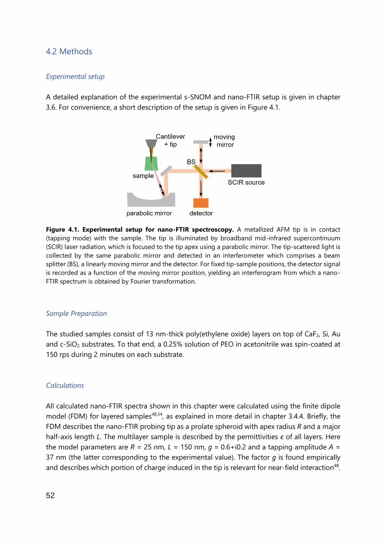
52
4.2 Methods
Experimental setup
A detailed explanation of the experimental s-SNOM and nano-FTIR setup is given in chapter
3.6. For convenience, a short description of the setup is given in Figure 4.1.
Figure 4.1. Experimental setup for nano-FTIR spectroscopy. A metallized AFM tip is in contact
(tapping mode) with the sample. The tip is illuminated by broadband mid-infrared supercontinuum
(SCIR) laser radiation, which is focused to the tip apex using a parabolic mirror. The tip-scattered light is
collected by the same parabolic mirror and detected in an interferometer which comprises a beam
splitter (BS), a linearly moving mirror and the detector. For fixed tip-sample positions, the detector signal
is recorded as a function of the moving mirror position, yielding an interferogram from which a nano-
FTIR spectrum is obtained by Fourier transformation.
Sample Preparation
The studied samples consist of 13 nm-thick poly(ethylene oxide) layers on top of CaF2, Si, Au
and c-SiO2 substrates. To that end, a 0.25% solution of PEO in acetonitrile was spin-coated at
150 rps during 2 minutes on each substrate.
Calculations
All calculated nano-FTIR spectra shown in this chapter were calculated using the finite dipole
model (FDM) for layered samples48,54, as explained in more detail in chapter 3.4.4. Briefly, the
FDM describes the nano-FTIR probing tip as a prolate spheroid with apex radius R and a major
half-axis length L. The multilayer sample is described by the permittivities ϵ of all layers. Here
the model parameters are R = 25 nm, L = 150 nm, g = 0.6+i0.2 and a tapping amplitude A =
37 nm (the latter corresponding to the experimental value). The factor g is found empirically
and describes which portion of charge induced in the tip is relevant for near-field interaction48.
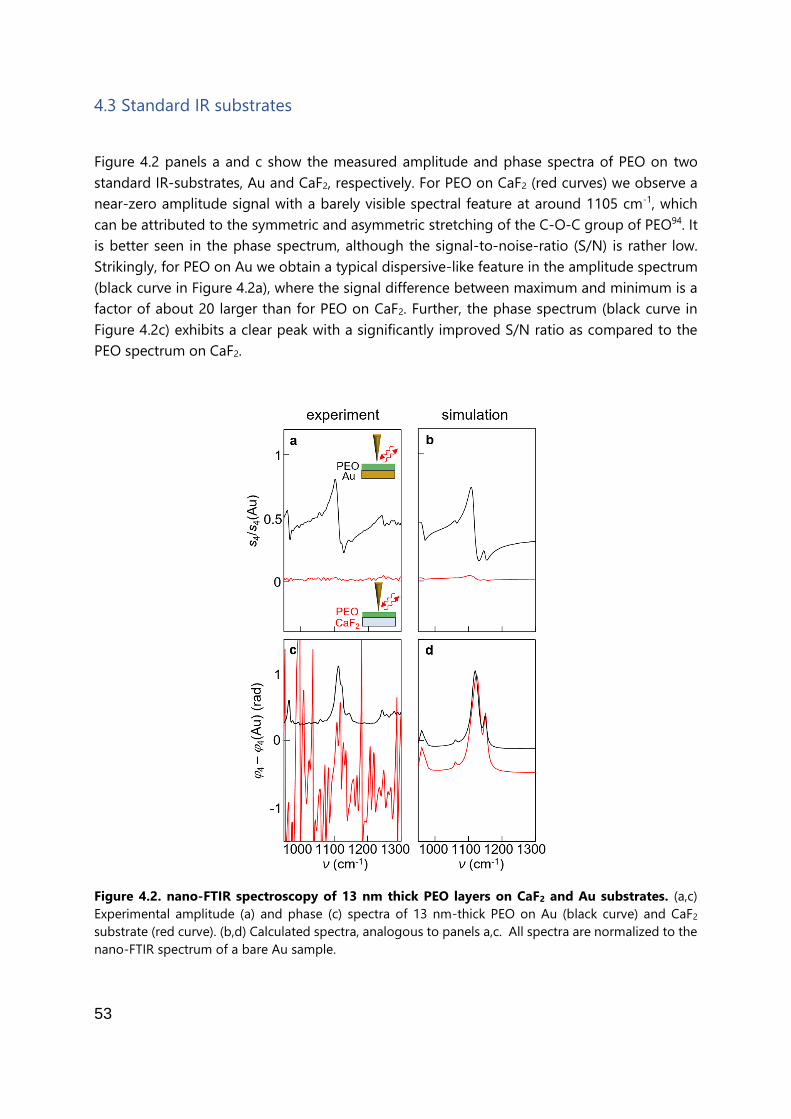
53
4.3 Standard IR substrates
Figure 4.2 panels a and c show the measured amplitude and phase spectra of PEO on two
standard IR-substrates, Au and CaF2, respectively. For PEO on CaF2 (red curves) we observe a
near-zero amplitude signal with a barely visible spectral feature at around 1105 cm-1, which
can be attributed to the symmetric and asymmetric stretching of the C-O-C group of PEO94. It
is better seen in the phase spectrum, although the signal-to-noise-ratio (S/N) is rather low.
Strikingly, for PEO on Au we obtain a typical dispersive-like feature in the amplitude spectrum
(black curve in Figure 4.2a), where the signal difference between maximum and minimum is a
factor of about 20 larger than for PEO on CaF2. Further, the phase spectrum (black curve in
Figure 4.2c) exhibits a clear peak with a significantly improved S/N ratio as compared to the
PEO spectrum on CaF2.
Figure 4.2. nano-FTIR spectroscopy of 13 nm thick PEO layers on CaF2 and Au substrates. (a,c)
Experimental amplitude (a) and phase (c) spectra of 13 nm-thick PEO on Au (black curve) and CaF2
substrate (red curve). (b,d) Calculated spectra, analogous to panels a,c. All spectra are normalized to the
nano-FTIR spectrum of a bare Au sample.

54
We corroborate the experimental nano-FTIR spectra and the substrate-induced signal
enhancement with calculations using the multilayer finite dipole model, in which the tip is
described as an elongated dipole48 that interacts with the several sample layers54 that are
characterized by their dielectric function. In this model, the tip-scattered field is given by
Escat ∝ (1+r)2αeff (4.1)
where αeff is the effective polarizability of the tip that accounts for the near-field interaction
between the tip and the layered sample. r is the far-field reflection coefficient of the substrate
(for calculation details see Methods). The calculated amplitude and phase spectra are shown
in Figure 4.2 panels b and d. We observe a remarkable agreement between experiment and
calculations, particularly regarding the strong enhancement of the vibrational signature in the
amplitude spectrum of the PEO layer on the Au substrate as compared to PEO on CaF2. This
signal amplitude enhancement is caused by (i) the large far-field reflection coefficient of Au (r
= 1) as compared to CaF2 (r = -0.06), which is the Fresnel reflection coefficient obtained for a
p-polarized wave at 60 degree incidence normal to the sample surface and a refractive index95
nCaF2 = 1.34 which leads to a more efficient tip illumination and collection of the tip-scattered
field, and (ii) the increased near-field interaction between tip and gold substrate yielding to a
stronger local field enhancement at the tip apex51,87. On the other hand, the calculated phase
spectra indicate that the phase contrast (peak height) of PEO on CaF2 is slightly larger than that
of PEO on Au. However, because of the much lower signal on CaF2 (see amplitude spectra), the
experimental S/N ratio is too low for this effect to be beneficial in a practical way.
Figure 4.3: Nano-FTIR amplitude as function of substrate permittivity. Calculated normalized nano-
FTIR amplitude s4/s4(Au) for semi-infinite substrates with varying permittivity Re(ϵ) and fixed Im(ϵ) = 0.2
(solid curve), respectively Im(ϵ) = 1.0 (dashed curve). Symbols highlight the results for substrates made
of gold (ϵAu = -5000+i1000) and calcium fluoride (ϵCaF2 = 1.8). For calculation details see Methods
section.

55
To illustrate the increased near-field interaction between tip and gold substrate, and to
generalize the results to other substrate materials, Figure 4.3 shows calculated nano-FTIR
amplitude signals s4/s4(Au) as a function of substrate permittivity ϵ and normalized to the
amplitude signals obtained on a gold substrate (black symbol). In good agreement with Figure
4.2, the amplitude signal obtained on a CaF2 substrate (red symbol) is significantly weaker than
that of a gold substrate. Strikingly, the calculated nano-FTIR amplitude increases far beyond
the level of a gold substrate when the substrate permittivity is slightly negative. We recall that
in most models for tip-sample near-field interaction the effective polarizability of the tip, αeff,
is a function of the near-field (quasi-electrostatic) reflection coefficient β, which for a semi-
infinite surface in vacuum is given by
β = (ϵ-1)
(ϵ+1) (4.2)
where ϵ is the dielectric function of the sample2,15,50,51. The effective polarizability, and thus the
tip-scattered field, exhibit a resonance near ϵ ≈ -1 (Figure 4.3) owing to the divergence of β,
which corresponds to the excitation of localized surface polaritons by the concentrated near
fields at the tip apex (e.g. surface plasmon polaritons in metals and doped semiconductors, or
surface phonon polaritons in polar crystals50). In Ref. 51 we predicted that this resonant near-
field interaction could enhance the infrared spectral contrast of molecular vibrations of thin
layers in the tip-substrate gap. Up to date, however, this effect has not been demonstrated
experimentally. In the following we thus explore the possibility of further increasing the nano-
FTIR signals of PEO by resonant tip-substrate coupling.
4.4 Phonon polariton-resonant substrate
For a first experimental demonstration of surface-polariton enhanced nano-FTIR spectroscopy
of molecular vibrations, we selected crystalline quartz (c-SiO2) substrates, an exemplary polar
crystal supporting surface phonon polaritons96,97 near the molecular vibrational resonance of
PEO. The measured far-field reflectivity spectrum of c-SiO2 is shown in Figure 4.4a. It exhibits a
typical Reststrahlen band, where R ≈ 1. Within this band (between 1070 and 1220 cm-1), the real
part of the dielectric function, ϵ1, is negative, which in case of c-SiO2 is a consequence of
multiple phonon excitations. By fitting the far-field spectrum with Fresnel equations we
obtained the complex-valued dielectric function of c-SiO2, which is plotted in Figure 4.4b.
Around 1150 cm-1 we find ϵ1,c-SiO2 ≃ -1, such that the condition for a tip-induced polariton
resonance in the substrate is fulfilled near the PEO molecular vibrational resonance at 1105 cm-
1 (marked by vertical dashed line and defined by the maximum of ϵ2,PEO) that can be clearly
recognized in the dielectric function of PEO (Figure 4.4c). Indeed, the nano-FTIR spectrum of a
clean quartz surface (normalized to the spectrum of bare gold) reveals the expected
resonance96 (blue curve in Figure 4.5d) where the normalized amplitude signal s4/s4(Au) exhibits

56
values that are up to 3.5 (i.e. 3.5 times higher than that of the gold reference surface). The
multiple-peak structure of the spectrum (maxima at 1135 and 1170 cm-1) can be ascribed to
the presence of several phonon resonances contributing to the Reststrahlen band of quartz96.
Figure 4.4. Optical properties of the quartz substrate and of PEO molecules. (a) Reflectivity spectra
of bare quartz. (b) Real (black curve) and imaginary (dashed black curve) part of the dielectric function
obtained by fitting the Drude-Lorentz model to the quartz reflection spectrum using the RefFIT
software98. (c) Real (black curve) and imaginary (dashed black curve) part of the dielectric function of
PEO, obtained by fitting far-field transmission spectra of 500 nm thick PEO layers on CaF2 by the Drude-
Lorentz model using the RefFIT software. The gray shaded area indicates the Reststrahlen band of quartz
and the vertical dashed line indicates the resonance frequency νPEO of the PEO vibration.
To explore the effect of tip-quartz coupling on the nano-FTIR spectra of thin PEO layers, we
evaporated 30 nm of Au onto one half of the quartz substrate and spin-coated PEO as
described above. That way we obtained a PEO layer on gold and on quartz within one sample,
which allows for a reliable comparison of the two situations under the same experimental
conditions (same tip, as well as same microscope settings and adjustment).
We obtained self-assembled islands of PEO on top of the gold and quartz surfaces with a rather
homogeneous height of 13 nm and an average diameter of about 150 nm. The PEO areas are
clearly visible in the AFM image (1x0.5 µm2) shown in Figure 4.5b and in the s-SNOM image of
the same area taken at 1114 cm-1 (amplitude image, s4, Figure 4.5c). The formation of islands
offers the advantage that nano-FTIR spectra of adjacent regions of PEO on c-SiO2 and bare c-
SiO2, as well as of PEO on Au and bare Au, can be measured under the same experimental
conditions, thus allowing for a reliable comparison of spectra. Note that in both data analysis
and simulations we do not consider the island-like morphology of the PEO layer. The
measurements were done in the center of larger islands, which have a diameter of typically

57
100-200 nm, and thus can be considered in first approximation as an extended layer compared
to the tip of about 25 nm apex radius and corresponding spatial resolution.
In Figure 4.5d we compare nano-FTIR spectra of PEO on quartz with nano-FTIR spectra of pure
quartz. We observe a strong dip in the PEO spectrum at the position close to the peak
maximum of the pure quartz spectrum, which we attribute to the vibrational resonance of PEO
(marked by dashed line). This finding strongly resembles the features found in surface- and
antenna-enhanced infrared spectra (SEIRA) of molecules on resonant plasmonic antennas,
where Fano interference between the molecular vibration and plasmons occurs99,100.
Analogously, we can explain the observation in our nano-FTIR spectra by Fano interference
between the molecular vibration and the tip-induced phonon-polariton in the substrate, similar
to phononic SEIRA101.
Figure 4.5. nano-FTIR spectroscopy on a resonant quartz substrate. (a) Topography line profile along
the red line in panel b). (b) Topography and (c) s-SNOM image recorded at ν = 1114 cm-1 (shown for
illustrative purposes only) of a 1x0.5 µm2 c-SiO2 substrate with spin-coated PEO on top, the latter forming
nanoscale islands. (d) Experimental and (f) calculated nano-FTIR amplitude spectra (4th harmonics,
normalized to gold spectrum) of quartz (blue) and PEO on quartz (red). Panels (e) and (g) show the
normalized quartz spectra (blue dashed curves) used for calculating the maximum spectral contrast C
(defined as difference between maximum and minimum of Δs4 shown by black curves) of the polariton-
enhanced vibrational feature of PEO on quartz for experimental and calculated data, respectively.
We measure the magnitude of the polariton-enhanced molecular vibrational signature
analogously to what is conventionally done in SEIRA measurements. We first subtract the
spectrum of PEO on quartz from the spectrum of bare quartz and then calculate the difference
between maximum and minimum of the resulting spectral feature (as illustrated in Figure 4.5e).
To apply this procedure, we need to take into account the reduced tip-substrate coupling

58
caused by the increased tip-substrate distance when the tip is on top of PEO. To that end, we
normalized the spectrum of quartz, s4(c-SiO2)/s4(Au), in such a way that the signal between
980-1050 cm-1 (assumed to be barley affected by the PEO vibration because of its rather large
spectral distance to the phonon resonance) matches with the one of the spectrum of PEO on
quartz, s4(PEO on c-SiO2)/s4(Au). We denote the resulting spectrum s4̅(c-SiO2)/s4(Au) and
show it as blue dashed line in Figure 4.5e. With ∆s4 = s4̅(c-SiO2)/s4(Au)-
s4(PEO on c-SiO2 )/s4(Au) we finally obtain the polariton-enhanced vibrational spectral contrast
(black curve in Figure 4.5e). Although our normalization step does not take into account the
spectral shifts caused by the increased tip-substrate distance102,103 we can reliably determine
the enhancement of C on c-SiO2 as compared to Au (for a comparison of different
normalization procedures, see Appendix 6.1).
The spectral contrast ∆s4 exhibits an asymmetric shape, neither resembling the amplitude nor
the phase spectrum of PEO on CaF2 or Au substrates. This observation is typical for a Fano-
type interaction between a broad excitation (the phonon polaritons in this case) and a narrow
mode (the PEO vibration), where the spectral shape depends on both the interaction strength
and on the spectral overlap between the two modes99. Most importantly, the spectral contrast
∆s4 is larger than the one obtained for PEO on Au, as we will highlight and quantify below.
Before, we corroborate the experimental results by calculations using the multilayer finite
dipole model described above. As shown in Figure 4.5 panels f,g, the spectral behavior is well
reproduced and the enhancement of the vibrational contrast is confirmed. We note that the
near-field phase contrast ∆s4 (data not shown) is barely enhanced. For that reason, we analyze
in this work essentially near-field amplitude spectra.
In the following, we compare quantitatively the enhancement factors of the PEO vibrational
signature in the case of non-resonant substrates with different reflection coefficients (CaF2, Si,
Au) and resonant c-SiO2. The results are summarized in Figure 4.6b. The three top curves show
the amplitude spectra of PEO on CaF2 (green), Si (orange) and Au (black). Taking the maximum
spectral contrast of the PEO on the Au substrate (C = 0.46) as a reference, we find a reduction
of C to 54% for PEO on Si and to 7% for the CaF2 substrate. This finding can be explained by
(i) the reduced reflection coefficient r of Si and CaF2 compared to Au (rSi = 0.28, rCaF2 = -0.06,
rAu = 1)95 which reduces both the illumination and scattering of the tip via the substrate (top
illustration of Figure 4.6a), and (ii) the reduced near-field interaction between tip and substrate
owing the smaller near-field reflection coefficient β (Equation (4.2)) of Si and CaF223. When PEO
is placed on c-SiO2 we achieve a 300% increase (compared to Au substrate) of C, which is
determined according to the procedure described above from the red spectrum shown as inset.
We can explain this significant enhancement compared to Au only by the enhanced near-field
interaction (described by αeff) between tip and substrate due to tip-induced phonon polariton
excitation, as tip illumination and tip scattering via the substrate reaches is maximum for the
Au surface (we stress that r is the far-field Fresnel reflection coefficient of the substrate, which
cannot exeed r = 1). Actually, the tip illumination and tip scattering via the quartz surface
reduces the signal amplitude by Abs[(1+rc-SiO2)2/(1+rAu)
2] ≈ 50%, which is, however, more
than compensated by the enhanced near-field interaction. Note that a native oxide is present
on the Si substrate, with a phonon-resonance at the position of the PEO vibrational mode.
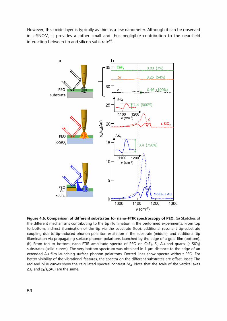
59
However, this oxide layer is typically as thin as a few nanometer. Although it can be observed
in s-SNOM, it provides a rather small and thus negligible contribution to the near-field
interaction between tip and silicon substrate69.
Figure 4.6. Comparison of different substrates for nano-FTIR spectroscopy of PEO. (a) Sketches of
the different mechanisms contributing to the tip illumination in the performed experiments. From top
to bottom: indirect illumination of the tip via the substrate (top), additional resonant tip-substrate
coupling due to tip-induced phonon polariton excitation in the substrate (middle), and additional tip
illumination via propagating surface phonon polaritons launched by the edge of a gold film (bottom).
(b) From top to bottom: nano-FTIR amplitude spectra of PEO on CaF2, Si, Au and quartz (c-SiO2)
substrates (solid curves). The very bottom spectrum was obtained in 1 µm distance to the edge of an
extended Au film launching surface phonon polaritons. Dotted lines show spectra without PEO. For
better visibility of the vibrational features, the spectra on the different substrates are offset. Inset: The
red and blue curves show the calculated spectral contrast ∆s4. Note that the scale of the vertical axes
∆s4 and s4/s4(Au) are the same.

60
4.5 Additional tip illumination by propagating surface phonon-polaritons
We finally explore the possibility of further boosting the enhancement of the vibrational
contrast by exploiting additional tip illumination via propagating surface phonon polaritons.
To that end, we deposited an extended gold film on quartz. The gold edge serves as a surface
phonon polariton (SPhP) launcher104 (see sketch in Figure 4.6a, bottom). When the tip is placed
close to the gold edge, i.e. within the propagation length of the SPhPs, the polariton field
provides an additional (coherent) tip illumination, thus boosting the near-field enhancement
at the tip apex. The experimental verification of this concept is shown by the spectra (blue) of
Figure 4.6b. The dashed blue curve represents the spectrum of quartz taken at 1 µm distance
from the gold edge. The signal amplitude is up to 12 times higher than the signal on gold, and
approximately 3 times higher than the signal of quartz far from the Au edge. We explain this
significant additional signal enhancement by (i) the high reflection coefficient r of Au (which –
as explained above – increases the signal amplitude by a factor of 2 compared to quartz) and
(ii) the additional tip illumination through the SPhP (both aspects illustrated in the sketch of
Figure 4.6a). We estimate that the additional tip illumination through the SPhP enhances the
signal amplitude by an additional factor of about 1.5.
To verify that the gold edge indeed launches a surface phonon polariton, we recorded a large
s-SNOM image (Figure 4.7 panels a,b) at 1114 cm-1 (photon wavelength λ = 9.0 µm) provided
by a quantum cascade laser (MIRcat, Daylight Solutions). We see fringes parallel to the gold
edge with a spacing of d = 24 µm, caused by the interference of the SPhP field with the incident
field at the position of the tip apex56,104. For α = 42° (angle of incidence with respect to the
sample surface) we obtain a SPhP wavelength of λSPhP = 8.1 µm according to
λSPhP = λd/[λ+d cos α], matching the calculated SPhP wavelength using the relation
2π/λSPhP = Re[ω c⁄ √ϵc-SiO2 (ϵc-SiO2+1)⁄ ]. Note that for this s-SNOM experiment the laser focus
size had to be enlarged significantly as compared to the nano-FTIR experiments, in order to
illuminate both tip and gold edge for distances as large as 100 µm, which is required for
unambiguous observation of the interference fringes.
We apply the edge-launched SPhPs for enhancing nano-FTIR signals and measure the
spectrum of PEO on quartz at 1 µm distance from the gold edge (solid blue curve in Figure
4.6b). By determining the spectral contrast ∆s4 (blue curve, inset of Figure 4.6b) we obtain C =
3.4, which corresponds to 750% of the value obtained for PEO on the Au substrate and almost
1400% of the value obtained on Si, the latter being the standard nano-FTIR substrate.
We note that the value of C oscillates with distance to the gold edge according to the local
field at the tip apex that is governed by the interference between the incident and SPhP field
(Figure 4.7b), which we demonstrate by measuring nano-FTIR spectra at various distances from
the gold edge. The spectra recorded on pure quartz (obtained when the tip is positioned in
between PEO islands, Figure 4.7c) clearly show a modulation of the peak maxima with
increasing distance from the Au edge. The peak height agrees well with the behavior of the s-
SNOM amplitude signal shown in Figure 4.7b. We then recorded the spectra of PEO on quartz,
at the same distances from the Au edge obtained when the tip is positioned on top of the PEO

61
islands, Figure 4.7d) and calculated the spectral contrast ∆s4 (Figure 4.7e). We find that the
spectral contrast indeed follows the local field above the quartz surface, which is determined
by the interference of the incident field and the field of the surface phonon polariton launched
at the gold edge.
Figure 4.7. s-SNOM images and nano-FTIR amplitude spectra of PEO on quartz substrate close to
a gold edge. (a) AFM topography image and (b) infrared amplitude image (recorded at 1114 cm-1) of a
large area of PEO on quartz close to a gold edge (seen at the bottom). (c and d) nano-FTIR amplitude
spectra of quartz (c) and PEO on quartz (d), recorded at several distances (provided by the numbers
labeling the spectra) from the gold edge. (e) spectral contrast ∆s4 calculated at each distance.
4.6 Increased tip-substrate coupling on ultra-thin films
To gain further insights into the spectral contrast enhancement, particularly for thinner
molecular layers, we show simulations of nano-FTIR spectra in Figure 4.8 (experimentally we
could not achieve PEO layers thinner than 13 nm). Figure 4.8a shows spectra of 1 nm and 2 nm
thick PEO layers on the quartz substrate (brown and green curves, respectively) in comparison
to the 13 nm thick PEO layer on quartz (red curve) and the pure quartz spectrum (blue curve).
We clearly see a significant modification of the quartz spectrum caused by even these thin PEO
layers. Following the procedure described in Figure 4.5, we calculate the maximum spectral
contrast Cc-SiO2(d) of the molecular vibration of a PEO layer of thickness d on a quartz substrate.
The black curve in Figure 4.8b shows that for a few nanometer thick layer the spectral contrast
Cc-SiO2 is larger than that of a 13 nm thick PEO layer on a gold substrate. Cc-SiO2 reaches a

62
maximum around 10 nm PEO thickness, before it decreases with increasing d. We explain this
decrease by the decreasing tip-substrate near-field coupling. For a comparison, we show the
thickness-dependent spectral contrast CAu(d) for PEO layers on a gold substrate (black dashed
curve), highlighting that the enhancement of the PEO spectral contrast on the quartz substrate
increases for thinner PEO layers. This observation can be better appreciated by plotting the
ratio Cc-SiO2(d)/CAu(d) in Figure 4.8c (black curve). The increasing enhancement for thin layers
can be explained by the stronger surface phonon polariton excitation when the distance
between tip and quartz decreases.
Figure 4.8. Simulation of thickness-dependent spectra and spectral contrasts. (a) Calculated nano-
FTIR amplitude spectra of differently thick PEO layers on a quartz substrate. Inset: Spectral contrast ∆s4
of the differently thick PEO layers, analogous to Figure 4.5. (b) Maximum spectral contrast for differently
thick PEO layers on quartz and Au substrates, Cc-SiO2 and CAu (c) Ratio Cc-SiO2/CAu.
4.7 Summary and Conclusions
In summary, we first demonstrated the crucial role of highly reflecting substrates for enhancing
the infrared nanospectroscopy signals of thin molecular layers. Au substrates were found to
provide an about one order of magnitude enhancement of nano-FTIR spectral signatures as
compared to CaF2 substrates. Exploiting tip-induced surface phonon polariton excitation in
polar crystal substrates (here quartz), a further enhancement by a factor of 3 can be achieved.
An even further enhancement could be achieved by implementing additional tip illumination
which includes propagating surface polaritons, altogether boosting the nano-FTIR
spectroscopic signal of molecular vibrations by nearly one order of magnitude compared to
nano-FTIR employing Au substrates. Polariton-enhanced nano-FTIR spectroscopy - eventually

63
in combination with infrared-resonant tips105 - could open promising avenues for molecular
vibrational spectroscopy of very thin layers of analytes, monolayers or maybe even single
molecules. Finally, we speculate that polariton-enhanced near-field coupling could also boost
the sensitivity in tip-enhanced photothermal infrared nanospectroscopy41 and photo-induced
force microscopy43,44.
The enhancement of nano-FTIR spectroscopy by tip-induced resonant surface polariton
excitation could be realized with various substrates supporting either surface phonon
polaritons (polar crystals such as SiC or Al2O3)55, dielectrically loaded polar crystals that provide
stronger surface polariton confinement97,106 or surface plasmon polaritons. The latter exhibit
resonances at mid-infrared frequencies on highly doped semiconductors, offering the
advantage that the resonances can be spectrally shifted via the carrier concentration to match
specific molecular vibrations80 (illustrated in Figure 4.9 for a hypothetical semiconductor
material with various carrier concentrations). Strong resonances could be achieved with
semiconductors with large carrier mobilities, such as GaAs or InAs107–110. On the other hand,
tip-induced surface polariton excitation (as described in this work) cannot be achieved by
employing extended flat slabs (flakes) of uniaxial 2D materials (such as h-BN111) as a substrate,
as they do not support surface polaritons at the slab surface. Surface polaritons exist at the
flake edges112 but resonant coupling with the tip has not been reported yet. Nevertheless, it
might be worth exploring mechanisms to enhance nano-FTIR signals by exploiting graphene
plasmons113,114 or hyperbolic plasmon and phonon polaritons in multilayer 2D materials such
as h-BN111.
We finally note that focusing of surface polaritons onto the probing tip – independent of
polariton-resonant tip-substrate coupling - could further boost the nano-FTIR signals. This
could be accomplished, for example, with appropriately designed polariton launchers on
conventional polar crystals115, metal films or van der Waals material substrates116–118 as well as
on plasmonic91–93 and phononic resonators101,119–122. Although the required substrate
structuring might limit imaging applications, the combination of nano-FTIR with polariton
launchers and resonators could become a valuable platform for studying strong light-matter
interactions at the nanoscale, particularly of infrared light and molecular vibrations92,101.

64
Figure 4.9: Spectrally tuneable tip-substrate resonance on doped semiconductors. nano-FTIR
amplitude spectra normalized to gold, s4/s4(Au), calculated for a hypothetical semiconductor material
with varying plasma frequencies νp, damping coefficient γ = 0.3νp, high-frequency permittivity ϵ∞ = 2
and electron effective mass m* = me, where me is the free electron mass. The plasma frequency relates
to the carrier concentration N via νp2 = Ne2/(ϵ∞ϵ0m*), where e is the elementary charge and ϵ0 is the
vacuum permittivity.

65
5 Subsurface chemical nanoidentification by nano-FTIR
spectroscopy
Nano-FTIR spectroscopy based on Fourier transform infrared near-field spectroscopy allows for
label-free chemical nanocharacterization of organic and inorganic composite surfaces. The
potential capability for subsurface material analysis, however, is largely unexplored terrain. In
this chapter, nano-FTIR spectroscopy of subsurface organic layers is demonstrated, revealing that
nano-FTIR spectra from thin surface layers differ from that of subsurface layers of the same
organic material. Further, the correlation of various nano-FTIR peak characteristics is studied,
thereby establishing a simple and robust method for distinguishing surface from subsurface layers
without the need of theoretical modelling or simulations (provided that chemically induced
spectral modifications are not present). The experimental findings are confirmed and explained
by a semi-analytical model for calculating nano-FTIR spectra of multi-layered organic samples.
The results are critically important for the interpretation of nano-FTIR spectra of multilayer
samples, particularly to avoid that geometry-induced spectral peak shifts are explained by
chemical effects.
5.1 Introduction
S-SNOM and nano-FTIR are often considered to be surface characterization techniques,
however, the finite penetration depth of near fields into the sample allows for subsurface
probing of nanoscale structures and defects up to a depth of 100 nm.19,20,24,28,123 For s-SNOM it
has been also shown that depth-resolved information – with the potential of three-dimensional
sample reconstruction - can be obtained by analysis of several higher harmonic signals, each
of them having a different probing depth.23,25–27 However, the potential capability for chemical
identification of subsurface material by nano-FTIR experiments is largely unexplored terrain.
In this chapter, an experimental and theoretical nano-FTIR spectroscopy study of thin
subsurface organic layers is presented. It is demonstrated (i) that nano-FTIR peaks of
subsurface layers are shifted to lower frequency as compared to that of bulk materials or thin
surface layers, and (ii) that surface and subsurface layers can be differentiated by analyzing the
ratio of peak heights obtained at different demodulation orders n, without theoretical
modelling or simulations. To that end, an exemplary study of the well-defined C = O vibrational
mode of a thin polymethyl-methacrylate (PMMA) layer on silicon covered by a polystyrene (PS)
layer of varying thickness is performed and then compared with differently thick uncovered
PMMA layers on silicon. It is further elucidated how a semi-analytical model can be used to
understand and predict nano-FTIR spectra of multi-layered samples. Finally, the validity and
applicability of the findings for a large variety of materials is demonstrated, by summarizing
and discussing the results of an extended theoretical and experimental study of the nano-FTIR
peak characteristics of differently thick subsurface layers exhibiting various molecular
vibrational modes. The results were previously published in Nature Communications (Ref. 22).

66
5.2 Systematic nano-FTIR spectroscopy study of subsurface organic layers
For subsurface infrared near-field spectroscopy we use the experimental s-SNOM and nano-
FTIR setup explained in chapter 3.6. For convenience, a short description of the setup is given
in Figure 5.1a. Importantly, the AFM tip acts as an optical antenna and creates strongly
enhanced near fields around the tip apex, yielding a spatial resolution in the order of the tip
radius, here R = 25 nm. Furthermore, the near fields penetrate into the sample (Figure 5.2b),
thus allowing for probing of subsurface material. For a quantitative analysis of subsurface
nano-FTIR spectra, all spectra in this chapter are normalized to the nano-FTIR spectrum of a
clean silicon substrate via σnnorm = σn/σn
Si. We focus our analysis on organic sample systems and
thus evaluate normalized nano-FTIR phase spectra φnnorm(ν) = Arg[σn/σn
Si], which qualitatively
relate to the absorptive properties of molecular samples.19,85,88,124 The superscript norm is
omitted in the following for simplicity.
Figure 5.2: Experimental s-SNOM and nano-FTIR setup. (a) Illustration of the s-SNOM and nano-FTIR
setup. A quantum cascade laser (QCL) is used for s-SNOM imaging. An infrared laser continuum based
on difference frequency generation (DFG) is used for nano-FTIR spectroscopy. The light source is
selected with a flip mirror (FM). A parabolic mirror (PM) is used for focusing the laser radiation onto the
tip apex. After collection of the tip-scattered light with the PM, a Michelson interferometer comprising
a beam splitter (BS) and moveable reference mirror (RM) is used for detection. (b) Near-field distribution
|E|2 around the tip apex (30 nm radius) of a 10 µm-long silicon cone with 20 nm-thick gold coating
located 2 nm above a sample comprised of a 10 nm-thick PS layer (with permittivity ϵPS=2.5)125 on PMMA
(with permittivity ϵPMMA = 1.52+i0.83)126. Simulated with the COMSOL Multiphysics software based on
the finite element method, for an illumination wavelength λ = 5.75 µm, corresponding to ν = 1739 cm-1,
at illumination angle of 60° with respect to the sample surface normal.
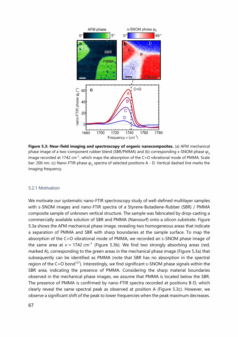
67
Figure 5.3: Near-field imaging and spectroscopy of organic nanocomposites. (a) AFM mechanical
phase image of a two-component rubber blend (SBR/PMMA) and (b) corresponding s-SNOM phase φ3
image recorded at 1742 cm-1, which maps the absorption of the C=O vibrational mode of PMMA. Scale
bar: 200 nm. (c) Nano-FTIR phase φ3 spectra of selected positions A - D. Vertical dashed line marks the
imaging frequency.
5.2.1 Motivation
We motivate our systematic nano-FTIR spectroscopy study of well-defined multilayer samples
with s-SNOM images and nano-FTIR spectra of a Styrene-Butadiene-Rubber (SBR) / PMMA
composite sample of unknown vertical structure. The sample was fabricated by drop-casting a
commercially available solution of SBR and PMMA (Nanosurf) onto a silicon substrate. Figure
5.3a shows the AFM mechanical phase image, revealing two homogeneous areas that indicate
a separation of PMMA and SBR with sharp boundaries at the sample surface. To map the
absorption of the C=O vibrational mode of PMMA, we recorded an s-SNOM phase image of
the same area at ν = 1742 cm-1 (Figure 5.3b). We find two strongly absorbing areas (red,
marked A), corresponding to the green areas in the mechanical phase image (Figure 5.3a) that
subsequently can be identified as PMMA (note that SBR has no absorption in the spectral
region of the C=O bond127). Interestingly, we find significant s-SNOM phase signals within the
SBR area, indicating the presence of PMMA. Considering the sharp material boundaries
observed in the mechanical phase images, we assume that PMMA is located below the SBR.
The presence of PMMA is confirmed by nano-FTIR spectra recorded at positions B-D, which
clearly reveal the same spectral peak as observed at position A (Figure 5.3c). However, we
observe a significant shift of the peak to lower frequencies when the peak maximum decreases.

68
As we can exclude peak shift due to chemical interaction128,129, we speculate that the peak shifts
are due to the subsurface location of PMMA. To corroborate subsurface nano-FTIR
spectroscopy of organic materials and to confirm that it comes along with significant peak
shifts, we performed a fundamental comparative study of multilayer organic samples with well-
defined composition and geometry, as described in the following.
5.2.2 Experiments on PMMA/PS test sample
As model sample for subsurface nano-FTIR spectroscopy we have chosen a PMMA layer of
thickness t2 = 59.4±4.7 nm on a silicon substrate that is covered by a PS layer of varying
thickness d2 = 0 to 110 nm (see schematics and AFM line profile in Figure 5.4a). The sample
was fabricated by spin-coating a 2% solution of PMMA (molecular weight 495 kDa) dissolved
in Anisole at 6000 rpm for 60 s onto a clean silicon substrate and subsequently annealing the
sample at 180 °C for 90 s to achieve a smooth PMMA surface. PS was spin-coated using the
same parameters (but no annealing) on two identical PMMA surfaces as 1.5% and 3% solution
in 1-chloropentane (yielding a different range of PS thickness depending on the concentration).
We chose 1-chloropentane as chemically selective solvent for PS to ensure a sharp interface
between the layers.130 The wedge shape was obtained by tilting the sample at an angle of ∼15°
during the PS spin coating step. The heights of the PMMA and PS layers were determined by
AFM height measurements, after the underlying silicon substrate was scratched free with
freshly cleaned tweezers. Reference nano-FTIR phase spectra of PMMA and PS are shown in
Figure 5.4b. We identify PMMA via the C=O vibrational stretch mode around 1738 cm-1.76 The
smaller plateau-like feature around 1440 to 1500 cm-1 corresponds to vibrations in the O-CH3
group. Characteristic for PS are the two distinct absorption lines at 1452 cm-1 and 1493 cm-1
(and a weaker mode at 1601 cm-1), which arise from C-C stretching vibrations in the aromatic
ring.131 The reference spectrum of PS does not exhibit any phase contrast around 1700 to
1800 cm-1, i.e. it is spectrally flat, which simplifies the following discussion.
Figure 5.4c shows subsurface nano-FTIR spectra of PMMA at different depths d2 below PS.
Without a capping layer (red, d2 = 0), we clearly observe the characteristic C=O and O-CH3
vibrational modes of PMMA. As the depth d2 of the PMMA layer (i.e. thickness t1 of the PS
capping layer) increases, the spectral feature from 1440 to 1500 cm-1 gradually changes from
plateau-like (which is characteristic for PMMA) towards two distinct peaks at 1452 cm-1 and
1493 cm-1 (which are characteristic for PS). Simultaneously, the C=O peak height (PMMA)
rapidly decreases with depth d2, but still allows for chemical identification of PMMA at a depth
of d2 = 110 nm. We note that the C=O peak shifts to lower frequencies (red shifts) with
increasing depth (indicated in Figure 5.4c by Δν3max), which reminds us of peak-shifts previously
reported in experimental nano-FTIR studies of surface PMMA layers18 and surface silicon
dioxide layers69 of varying thicknesses.
In order to better understand the nano-FTIR phase spectra, we focus our analysis on the C=O
peak of PMMA around 1738 cm-1. Specifically, we investigate the depth-dependence of the
spectral peak position νnmax and peak height φ
nmax (defined in the inset of Figure 5.5) for the

69
two different higher harmonic demodulation orders n = 3 and n = 4. For comparison, we
performed a similar study on thin PMMA layers of varying thickness t1 at the surface. The results
are shown in Figure 5.5 (large symbols).
Figure 5.4: Subsurface nano-FTIR spectroscopy experiments on well-defined multi-layer samples.
(a) Schematics of the experiment and PMMA/PS test sample, including the topography line profile of a
d2 = 85 nm-thick PS layer covering the t2 ≈ 59.4 nm-thick PMMA layer on Si. (b) Reference nano-FTIR
phase spectra recorded on thick PMMA and PS layers. (c) Subsurface nano-FTIR phase spectra of PMMA
at different depths d2 below PS (average of 50 spectra (80 spectra for d2 ≥ 85 nm), 30 s acquisition time
per interferogram, ×128 zero filling, 17 cm-1 spectral resolution). Black arrows in (c) indicate the spectral
peak-shift Δν3max.
70
Figure 5.5a,b show the results for the subsurface PMMA layer. We observe that the peak height
(Figure 5.5a) for both demodulation orders rapidly decreases when the depth d2 of the PMMA
layer (i.e. thickness of the PS capping layer) increases. This decay can be explained by the
exponential decay of the near fields from the tip apex into the sample (as seen in Figure 5.2b).
The deeper the PMMA layer, the less near fields it is absorbing, i.e. the less material is probed.
The C=O peak can still be identified at a depth of d2 = 110 nm. Further, we observe a red shift
of the peak position with respect to the peak position νref (horizontal line in Figure 5.5 panels
b,d) with increasing d2 (of up to Δν3max = νref - ν3
max = 7 cm-1 at d2 = 110 nm). Interestingly, we
find that signal demodulation at higher harmonics yields stronger red-shifts and a faster decay
of the peak height with increasing depth, that is, the relative contrast C = φ4max/φ
3max decreases
with increasing depth. We attribute this behavior to the stronger confinement of near fields to
the tip apex at higher demodulation orders20,21,27. We further analyze C below to distinguish
nano-FTIR spectra of subsurface layers from thin layers at the surface.
For comparison, Figure 5.5c,d show the results for the surface PMMA layers of varying thickness
t1. We observe that the peak height φnmax for both demodulation orders slowly decreases when
the thickness t1 of the PMMA layer decreases. This decay can be explained by the decreased
amount of absorbing material within the nano-FTIR probing volume. The thinner the PMMA
layer, the less near fields it is absorbing, i.e. more silicon is probed, which is non-absorbing in
this spectral range. Further, we see a red-shift of the peak position with decreasing t1 (of up to
Δν3max = 2 cm-1), as previously reported and explained by Mastel et al.18 A thin organic layer on
a highly reflective substrate promotes reflections of near fields between the tip and sample,
which changes the probing mechanism from absorption-like to an absorption-reflection
mechanism, thus causing a shift of the peak position.18 Interestingly, Figure 5.5 also shows that
the spectral peak shift in nano-FTIR phase spectra is much larger for subsurface layers when
compared to surface layers. Notably, and in contrast to the subsurface PMMA layers, we find
that the relative contrast C = φ4max/φ
3max and the spectral peak position for PMMA layers at the
sample surface vary only slightly with the demodulation order n, as we further analyze and
exploit below.

71
Figure 5.5: Comparison of PMMA subsurface layers and thin PMMA surface layers. (a,c) Peak
heights φnmax and (b,d) spectral peak positions νn
max extracted from experimental (large dots) and
calculated (lines) nano-FTIR phase spectra as a function of PMMA depth d2 (left column) and PMMA
thickness t1 (right column), for different demodulation orders n = 3 (red) and n = 4 (blue). The solid and
dashed lines are calculated with and without the far-field factor (1+r)² in Equation (1) respectively. The
gray horizontal dotted line indicates the peak position νref experimentally obtained on thick PMMA
surface layers. Inset: definition of φnmax and νn
max. Each experimental data point shows mean values and
standard deviation (error bars) obtained from 10 averaged (5×) spectra (16 averaged spectra for d2
≥ 85 nm).

72
5.2.3 Interpretation of nano-FTIR spectra of multi-layered samples
To better understand nano-FTIR spectra of vertically inhomogeneous samples, we performed
model calculations based on the finite dipole model (FDM), which is illustrated in Figure 5.6a
and explained in more detail in chapter 3.4.3. In short, s-SNOM signals are described by
calculating the scattering coefficient σ = Escat/E0, where E0 is the incident field and Escat is the
tip-scattered field. The tip is modelled as elongated spheroid with major half-axis length L and
tip apex radius R. It is illuminated directly and indirectly via reflection at the sample surface
with the far-field reflection coefficient r, yielding a local electric field at the tip, Eloc ∝ (1+r)E0,
which induces an electric dipole p0 in the tip. The near-field interaction of p
0 with the sample
is mediated predominantly via one of the charges associated with this dipole, Q0, located close
to the tip apex,13,48 which induces an additional dipole p1 in the tip. The total induced dipole
moment is p = p0 + p
1 = αeffEloc, where αeff is the effective polarizability of the coupled tip-
sample system. The scattered (far) field of this dipole is measured directly and via reflection
from the sample, Escat ∝ (1+r)p. The scattering coefficient can thus be described by
σ = (1+r)2αeff. (5.1)
In the FDM the effective polarizability is given by 13,48
αeff = 1+1
2
f0(H)β(ϵ)
1 - f1(H)β(ϵ), (5.2)
where β = (ϵ-1)/(ϵ+1) is the quasi-electrostatic reflection coefficient of a semi-infinite (bulk)
sample with permittivity ϵ, and fi(H) (given in Equation (3.23)) describe the tip geometry and
tip-sample distance H(t) = A(1+ cos Ωt ). The higher harmonic signal demodulation (used for
background suppression) is included in the model as explained in chapter 3.3 by taking the nth
Fourier coefficient F̂n with respect to time, yielding the nth-order demodulated scattering
coefficient 13,48
σn = (1+r)2F̂n [1+1
2
f0(H(t))β
1 - f1(H(t))β]. (5.3)
To facilitate the interpretation of Equation (5.3) in the following, we express the scattering
coefficient as Taylor series in β of order N,52 such that nano-FTIR signals are simply proportional
to powers j of β:
σn ≈ (1+r)2⋅1
2∑ F̂n [f0f1
j-1⋅β
j]
N
j=1
, (5.4)
which is valid for weak molecular oscillators with |β| < 1 (which includes for example polymers
and biological matter).

73
Figure 5.6: Illustration of the finite dipole model for bulk and multi-layered samples. (a) The nano-
FTIR tip is modelled as a prolate spheroid of length 2L and apex radius R, which is located at height H(t)
above a bulk sample with permittivity ϵ and electrostatic reflection coefficient β = (ϵ-1)/(ϵ+1). The
incident electric field E0 induces the primary electric dipole p0, which interacts with the sample via the
point charge Q0, yielding the near-field induced dipole p1 (indicated by red curved arrows). The model
accounts for far-field illumination and detection of the tip-scattered field Escat via reflection at the sample
surface, described by the Fresnel reflection coefficient r (indicated by red straight arrows). (b-c)
Illustration of (b) monopole field reflected at a multilayer sample, Ez,refl, and (c) monopole field Ez without
sample. Both red dashed arrows have a length of 2za. The multilayer sample in (b) is characterized by
the quasi-electrostatic reflection coefficient β(q), which is obtained from the single-interface electrostatic
reflection coefficients βij and layer thicknesses t
j.
Equations (5.3) and (5.4) can be used to calculate relative material contrasts in nano-FTIR
spectroscopy, however, they are valid only for semi-infinite samples. To extend the model to
multi-layered samples, we use the multi-layer reflection coefficient β(q) which depends on the
momentum q and for one layer on a substrate it is given by 18,54
β(q) = β
01+β
12exp(-2qt1)
1+β01
β12
exp(-2qt1), (5.5)
where βij = (ϵj - ϵi)/(ϵj + ϵi) are the single-interface reflection coefficients and t1 is the layer
thickness, as indicated in Figure 5.6b. Multiple layers on a substrate can be described by
recursively using Equation (5.5) as expression for β12
.51 The FDM (Equation (5.3) and (5.4)),
however, does not explicitly support momentum-dependent reflections (because the quasi-
74
static approximation q → ∞ is made). Instead of using the FDM for layered samples by Hauer
et al. (chapter 3.4.4), we substitute β in Equation (5.3) and (5.4) by the effective near-field
reflection coefficient β̅ = Ez,refl/Ez, where Ez,refl is the electric field produced by an effective point
charge Qa (located at a distance za from the sample surface, Figure 5.6b), reflected at the multi-
layered sample surface and evaluated at the position of Qa itself (indicated by red dashed arrow
in Figure 5.6b). Ez is the electric field of Qa at a distance of 2za (Figure 5.6c). It can be shown
(see Appendix 6.3) that
β ̅ = Ez,refl
Ez
= ∫ β(q)qe-2qza
∞
0dq
∫ qe-2qza∞
0dq
, (5.6)
where za = H(t) + a. Here a describes the height of the effective charge Qa above the tip apex.
The value a will be found such that good agreement between calculation and experiment is
achieved. In contrast to the description by Hauer et al. (Equation (3.27)), the effective reflection
coefficient β̅ in Equation (5.6) can directly be interpreted as the weighted average of β(q),
averaged over momenta q with the weight of each q given by qe-2qza . As further discussed
below, this allows to directly relate nano-FTIR spectra to the sample’s Fresnel reflection
coefficient.
We use Equations (5.4) and (5.6) to calculate nano-FTIR phase spectra φn(ν) of surface and
subsurface PMMA layers corresponding to the sample geometries of Figure 5.5 and extract the
spectral peak positions νnmax and peak heights φ
nmax for various layer thicknesses and depths.
PMMA is described by dielectric permittivity data obtained by infrared ellipsometry126 and we
assume PS and Silicon to be non-absorbing in the considered spectral range, with ϵPS = 2.5
and ϵSi ≈ 11.7.95,125 The employed model parameters are: A = 30 nm, R = 30 nm, L = 200 nm, g
= 0.65 (g describes the amount of induced charge that is relevant for the near-field
interaction13,48). Convergence of the calculated νnmax and φ
nmax (red and blue lines for
demodulation orders n = 3 and n = 4, respectively) is achieved for Taylor expansion orders
N ≥ 5, and we find good agreement with the experimental data for a = 1.4R. The effective
charge Qa is thus located slightly higher than the charge Q0 (located at distance R from the tip
apex), indicating that the near-field interaction takes place also via the apex-near part of the
tip shaft, which is located further away than the tip apex. Indeed, probing of subsurface layers
is frequently attributed to the elongated tip shape, which provides longer-reaching evanescent
waves (with lower momenta q) that are not captured well by the unmodified FDM for bulk
samples.24,54,69
Note that for large subsurface layer depths d2 ≥ 30 nm we observe a dispersive line shape in
the experimental nano-FTIR spectra (Figure 5.4c). We attribute this finding to the far-field
reflection of both the illumination and tip-scattered field at the sample surface (considered in
Equation (5.1) by the far-field refection coefficient r), which carries the far-field absorption
characteristics of the subsurface PMMA layer. This PMMA far-field contribution to the tip-
scattered field becomes notable when the near-field contribution vanishes at larger probing
depths. We support our explanation with Figure 5.7, where we compare calculated nano-FTIR
peak shapes, revealing that the far-field factor (1+r)² in Equation (5.1) indeed yields a dispersive

75
line shape for large d2. For a more quantitative comparison we show in Figure 5.5 the calculated
peak positions and peak heights obtained without the far-field reflection coefficient (dashed
lines). We find that for d2 < 20 nm the peak positions are nearly the same as for the calculation
including the factor (1+r)² (solid lines), revealing that the peak shift is essentially a near-field
effect. For d2 > 20 nm, the peak shift stays rather constant and clearly differs from the
calculation including the factor (1+r)². The continuous red shift for d2 > 20 nm observed in the
experiment can be thus attributed to the far-field contribution. We note that the constant peak
position for d2 > 20 nm does not imply the absence of near-field probing. The peak height still
decreases until d2 > 100 nm, which is a clear near-field signature. We finally note that for layers
of lateral extensions smaller than the illumination wavelength we expect the contribution from
the far-field reflection becoming less pronounced, yielding peak shifts located between the
dashed and solid curves in Figure 5.5.
Figure 5.7: Calculated nano-FTIR phase spectra with and without far-field reflection at sample.
Calculated nano-FTIR phase spectra of a t2 = 59 nm-thin subsurface PMMA layer on a silicon substrate,
located at depth (a) d2 = 75 nm and (b) d2 = 150 nm below PS. Dashed and solid lines are calculated
with and without the factor (1+r)² in Equation (5.1), which accounts for far-field illumination and
detection via the sample surface. Vertical gray lines indicate peak positions. The figure shows that the
factor (1+r)² yields an additional red-shift of the peak (panel a) and an increasingly pronounced
dispersive line shape with increasing depth of the subsurface layer. Note that in the experiment this
effect appears already at smaller depth d2.

76
5.2.4 Relating nano-FTIR spectra to the Fresnel reflection coefficient
The analytical nature of our model lets us elucidate the physical cause of the spectral peak
shifts observed in nano-FTIR phase spectra of multi-layered samples. Our model (Equations
(5.4) and (5.6)) shows that the spectral behavior of nano-FTIR signals essentially follows the
spectral behavior of β̅, as neither the exponent j nor the geometry-factors f0 and f1 in Equation
(5.4) lead to spectral peak shifts. Furthermore, β̅ can be interpreted as weighted average of
β(q), with the weights being determined by the (spectrally independent) coupling weight
function (CWF)
wFDM(q,H) = qe-2qza(H). (5.7)
To illustrate the spectral shifts, we compare in Figure 5.8 the phase of the Fresnel reflection
coefficient, Arg β(ν,q), for three PMMA samples with different geometries. The C=O vibrational
mode of PMMA is described by a dielectric function (plotted in Figure 5.8a), which can be well
described by a Lorentz oscillator. It can be thus considered a highly representative example of
a typical molecular vibration. Figure 5.8b shows Arg β(ν,q) of bulk PMMA. We find a spectral
maximum (traced by the vertical black line) at 1741 cm-1, which is independent of q. The
situation changes for a thin PMMA layer (thickness t1 = 20 nm) on a silicon substrate (Figure
5.8c). For decreasing q, we observe that the spectral maximum shifts to lower frequencies when
compared to bulk PMMA (as indicated by Δν in Figure 5.8c). Analyzing finally Arg β(ν,q) for a
subsurface PMMA layer (thickness t2 = 20 nm, on top of Si substrate and covered by a d2 = 40
nm-thick PS layer), we find that for all momenta q the spectral maximum is shifted to lower
frequencies compared to bulk PMMA (Figure 5.8d). This shift Δν is larger than that of thin
PMMA surface layers (Figure 5.8c) and increases with increasing q (contrary to the thin surface
layer). For a comparison with nano-FTIR phase spectra φn(ν) we have to consider that the nano-
FTIR tip provides and probes a broad distribution of momenta, which is described by the CWF,
i.e. for a tip-sample distance H = 0 (Figure 5.8e). Note that similar expressions for a CWF are
also found in mathematically rigorous s-SNOM models,54,58,59 however a direct correlation with
nano-FTIR spectra is less apparent due to the complexity of such models. Here, we multiply the
CWF (Figure 5.8e) with the Fresnel reflection coefficient (Figure 5.8b-d) and subsequently
integrate over all momenta q, and we obtain Arg β̅(ν) (Figure 5.8f), which we directly compare
with calculated nano-FTIR phase spectra φ3(ν) (Figure 5.8g). We find qualitative agreement
between the spectral shifts in Arg β̅(ν) and φ3(ν), indicating that the root cause of spectral
nano-FTIR shifts in layered samples are spectral shifts of the multilayer Fresnel reflection
coefficient and thus a true spectroscopic feature of the sample.
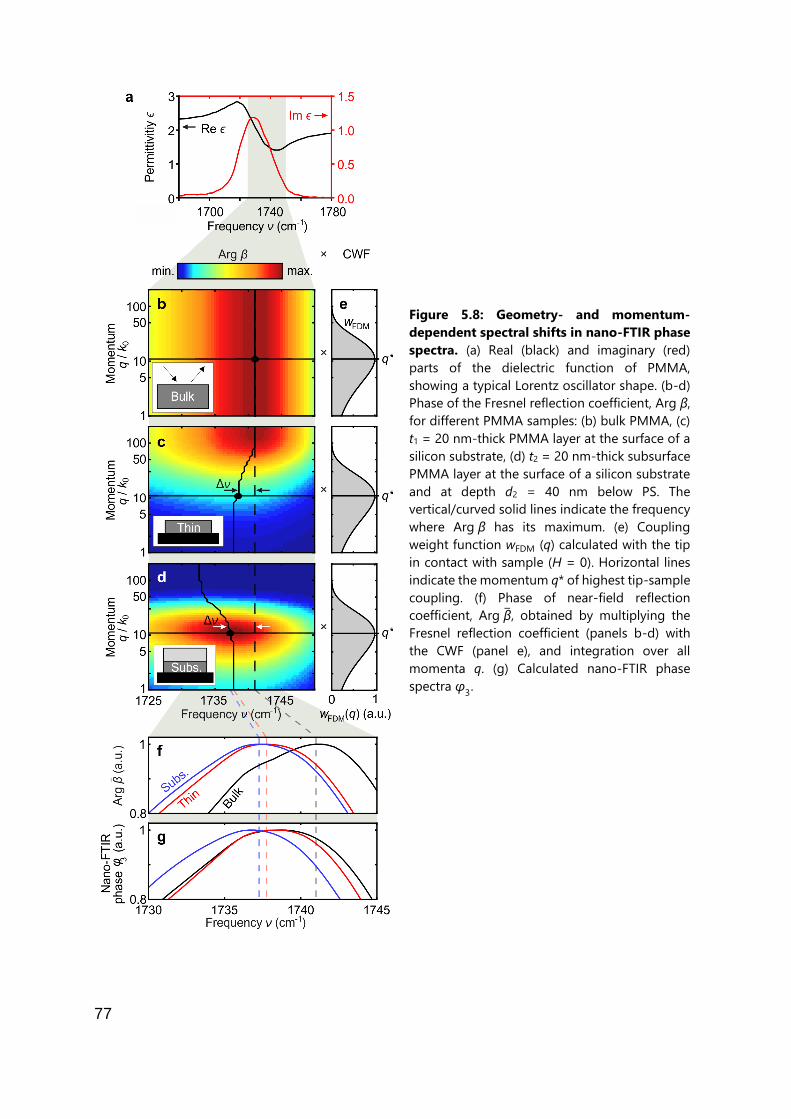
77
Figure 5.8: Geometry- and momentum-
dependent spectral shifts in nano-FTIR phase
spectra. (a) Real (black) and imaginary (red)
parts of the dielectric function of PMMA,
showing a typical Lorentz oscillator shape. (b-d)
Phase of the Fresnel reflection coefficient, Arg β,
for different PMMA samples: (b) bulk PMMA, (c)
t1 = 20 nm-thick PMMA layer at the surface of a
silicon substrate, (d) t2 = 20 nm-thick subsurface
PMMA layer at the surface of a silicon substrate
and at depth d2 = 40 nm below PS. The
vertical/curved solid lines indicate the frequency
where Arg β has its maximum. (e) Coupling
weight function wFDM (q) calculated with the tip
in contact with sample (H = 0). Horizontal lines
indicate the momentum q* of highest tip-sample
coupling. (f) Phase of near-field reflection
coefficient, Arg β̅, obtained by multiplying the
Fresnel reflection coefficient (panels b-d) with
the CWF (panel e), and integration over all
momenta q. (g) Calculated nano-FTIR phase
spectra φ3.

78
The quantitative differences between Arg β̅(ν) and φ3(ν) can be explained by signal
demodulation in nano-FTIR, which has not been considered so far in our analysis of β̅.
Equations (5.4) and (5.6) imply that signal demodulation (described by the Fourier components
F̂n) acts on the CWF, wFDM(q,H), which depends on the modulated tip-sample distance H. It is
well known20,26,27 that s-SNOM imaging at higher demodulation orders improves the lateral
spatial resolution and reduces the probing depths, indicating that near fields of larger
momenta are probed. This corresponds to near-field probing at higher momenta q for
increasing n, and explains the reduction of the nano-FTIR spectral peak shifts for surface layer
and an increase for subsurface layers (compared to bulk) observed in Figure 5.8g. As probing
with higher momenta implies better spatial resolution, we expect that inhomogeneities in
surface layers can be better resolved than in subsurface layers.
We point out that the observed peak shifts observed in nano-FTIR are not specific to near-field
spectroscopy. They also occur in far-field infrared spectroscopy, for example, when the
reflected power R = |r(ν,q)|2 is measured.132 This is because the far-field reflection
coefficient r(ν,q) depends – as well as the quasi-electrostatic near-field reflection coefficient –
on the momentum q = k0 sin(Θ), which in far-field spectroscopy is determined by angle of
incidence, Θ. We illustrate this dependence in Figure 5.9 by calculating the reflected power of
a 10 nm-thin PMMA layer on a silicon substrate that is illuminated under normal-incidence
(Θ = 0 degree, red) and grazing-incidence (Θ = 90 degree, blue). Figure 5.9c shows that in this
case a peak-shift of 10 cm-1 is observed.
Figure 5.9: Momentum-dependent spectral peak shifts in far-field infrared reflection
spectroscopy. Calculated reflected power |rp|2 of p-polarized infrared far-field radiation, reflected from
the surface of a 10 nm-thin PMMA layer on a silicon substrate (as illustrated in the inset), (a) for varying
in-plane momenta q which correspond to varying angles of incidence Θ via q = k0⋅sin(Θ) for a fixed
frequency ν = 1737 cm-1 near the C=O vibrational mode of PMMA, (b) for varying frequencies ν at
normal-incidence (Θ = 0°, red) and grazing-incidence (Θ = 80°, blue). (c) Same as panel b, but shown
after baseline subtraction and normalization for better visibility of the angle-dependent spectral peak-
shift Δν ≈ 10 cm-1.

79
5.3 Model-free differentiation of subsurface and surface layers
Finally, we elucidate how the observed spectral differences between nano-FTIR spectra of thin
organic layers at the surface and subsurface organic layers could be exploited for distinguishing
the two cases without the need of theoretical modelling, which is to date still a challenging and
time-consuming task. To this end, we analyze the correlation between peak height φ3max and
spectral peak position ν3max, as well as the correlation between peak height φ
3max and peak
height ratio C = φ4max/φ
3max. In Figure 5.10a,c (experimental and calculated data, respectively)
we observe that the peak position in nano-FTIR phase spectra of both thin PMMA surface layers
(black symbols) and PMMA subsurface layers (red symbols) show similar trends, i.e. that a
decrease in peak height comes along with a spectral red-shift. However, for subsurface layers
the red-shift is much stronger. The peak height ratio C = φ4max/φ
3max shows opposing trends for
thin PMMA surface and subsurface layers (experimental and calculated data in Figure 5.10b,d,
respectively). With decreasing peak height, we find that C increases for surface layers and
decreases for subsurface layers. We explain this correlation of C and peak height by the
reduced probing depth (and increased surface-sensitivity) at higher harmonic demodulation
orders.20,21,27 The reduced probing depth at higher harmonic demodulation orders (illustrated
in Figure 5.11) causes φ4max to decrease faster than φ
3max, as the depth d2 of a subsurface layer
increases – thus the ratio φ4max/φ
3max decreases for subsurface layers (Figure 5.11c,f). On the
other hand, as the thickness t1 of a surface layer decreases, the increased surface-sensitivity at
higher demodulation orders causes φ4max to reduce slower than φ
3max – thus the ratio φ
4max/φ
3max
increases for surface layers (Figure 5.11b,e).
In the calculations we also considered subsurface layers of different thicknesses t2. We find that
both the peak shifts and peak height ratios (red curves in Figure 5.10c,d respectively) are always
located below the curves obtained for the surface layers (black lines). Our observations thus
offer a rather easy procedure for distinguishing surface and subsurface layers. We assume that
the correlations for PMMA surface layers (black curves) are known from reference
measurements or can be approximated by a straight line connecting reference measurements
obtained for a very thin surface layer (leftmost black data points in Figure 5.10b,d) and a bulk
surface (rightmost black data points in Figure 5.10b,d). Sample measurements yielding data
points below the black reference curve (i.e. located within the areas marked by gray colors)
thus indicate that subsurface material is probed. Interestingly, when a data point exhibits both
a smaller peak height and a smaller peak height ratio than a PMMA bulk surface (i.e. is located
within the area marked by the dark gray color), we can conclude that the probed material is
below the surface even without reference measurements on thin surface layers. As discussed
below for various molecular vibrational bonds, the correlation of peak height ratios and peak
heights (Figure 5.10b,d) is a rather general and robust method for distinguishing surface and
subsurface layers.

80
Figure 5.10: Correlation of nano-FTIR peak characteristics. (a) Spectral peak positions ν3max and (b)
peak height ratios C of PMMA surface (black symbols) and PMMA subsurface (red symbols) layers are
plotted versus the corresponding peak heights φ3max (experimental data taken from Figure 5.4). Arrows
indicate decreasing PMMA surface layer thickness t1 (black) and increasing PMMA subsurface layer depth
d2 (red). Subsurface PMMA layer thickness is t2 = 59 nm. (c,d) Calculation results analogous to panels a
and b. Additionally, results for PMMA subsurface layers of thicknesses t2 = 15 nm (dotted red line) and
t2 = 100 nm (solid red line) are shown. (e) PMMA nano-FTIR peak positions ν3max and (f) peak height
ratios C are plotted versus the corresponding peak heights φ3max (data measured at positions A-D in
Figure 5.3b). (b,d,f) Gray areas indicate the data spaces that correspond to subsurface material.
Figure 5.11: Illustration of the peak height ratio criterium. (a-c) Schematic of the nano-FTIR
experiment employing different higher harmonic demodulation orders n = 3 (red) and n = 4 (blue) for
three samples with different geometries: (a) bulk material, (b) thin surface layers and (c) subsurface layers.
Gray areas mark the absorbing material. Ellipses below the tip illustrate the probing volumes. Graphs
illustrate the exponential decay of near fields Ez for different demodulation orders. (d-f) Sketch of
qualitative nano-FTIR phase spectra, corresponding to panels a-c. For a given n, all φn spectra are
normalized to φnmax of bulk.

81
We apply our findings to clarify the location of PMMA in the SBR/PMMA blend studied in
Figure 5.3. To that end, we plotted the spectral peak positions ν3max and peak height ratios C
recorded at positions A to D versus the corresponding peak heights φ3max (Figure 5.10 panels
e,f). We find that the peak position ν3max≈1738 cm-1 for the largest peak height φ
3max (position
A) agrees well with the peak position of a thick PMMA surface layer (compare Figure 5.10e with
Figure 5.10a). Together with the large peak height and the sharp material boundaries at the
sample surface observed in the AFM mechanical phase image (see description of Figure 5.3),
we conclude that at position A a thick PMMA surface layer is probed. As discussed above, we
use the data point recorded at position A as reference measurement to clarify the location of
PMMA at the points B to D. The combined reduction of C and φ3max (relative to position A) at
each of the positions B, C and D reliably reveals that a subsurface PMMA layer is probed (as
indicated in Figure 5.10f by the dark gray area analogous to Figure 5.10b,d). This conclusion is
supported in Figure 5.10e, where we observe strong spectral red-shifts down to
ν3max=1732 cm-1 as the peak height decreases (positions B-D), which is much stronger than that
for thin PMMA surface layers (black dots in Figure 5.10a and Mastel et al.18).
We note that for the discrimination of surface and subsurface layers one could apply nano-
FTIR peak ratios obtained from other demodulation orders n (for example the ratios φ4max/φ
2max
or φ3max/φ
2max, see Figure 5.12), as far as the respective near-field signals are background free
and of sufficiently large signal-to-noise ratio.
Figure 5.12: Comparison of calculated peak height ratios for different signal demodulation orders.
(a) φ4max/φ
3max, (b) φ
3max/φ
2max and (c) φ
4max/φ
2max of PMMA surface (black curve) and PMMA subsurface
(red curves) layers are plotted versus the corresponding peak heights φ3max. Arrows indicate decreasing
PMMA surface layer thickness t1 (black) and increasing PMMA subsurface layer depth d2 (red). Subsurface
PMMA layer thicknesses are t2 = 15 nm (dotted red line), t2 = 59 nm (dashed red line) and t2 = 100 nm
(solid red line). (a-c) Green areas indicate the data spaces that correspond to subsurface material. The
figure shows that peak height ratios obtained from various harmonics can be used to distinguish whether
and infrared absorbing layer is at the surface or below the surface.

82
5.4 Discussion
We have chosen to study the nano-FTIR peak characteristics of the C=O bond, as it represents
a typical molecular vibration. Being able to describe this vibration by a Lorenz oscillator model,
as most other molecular vibrational bonds, our findings regarding peak shifts and peak height
ratios can be assumed to be valid for most molecular vibrational bonds. To corroborate this
assumption, we performed a largely extended study. All results of this study are presented in
the Appendix 6.4 (Appendix Figures Figure 6.2 to Figure 6.10). In the following we briefly outline
the study and summarize and discuss the main results.
Appendix Figure 6.2 to Figure 6.4 present calculations of the momentum-dependent Fresnel
reflection coefficient, nano-FTIR peak shifts and peak height ratios for various C-C-O and C-O-
C bonds of surface and subsurface PMMA layers between 1100 cm-1 and 1300 cm-1. The
corresponding molecular vibrations differ not only regarding the chemical bonding, but also
in oscillator strength, and partially overlap spectrally. Analogous to Appendix Figure 6.2 to
Figure 6.4, the Appendix Figure 6.5 to Figure 6.6 show results obtained for surface and
subsurface polyethylene-oxide (PEO) layers, which exhibit three C-O stretching modes of
different oscillator strengths. The calculations are complemented by experimental results in
the Appendix Figure 6.7. We also calculated peak shifts and peak height ratios for surface and
subsurface layers modelled by a Lorenz oscillator with different high-frequency permittivity
(Appendix Figure 6.8). Finally, the nano-FTIR peak shifts and peak height ratios of the C=O
bond of PMMA subsurface layers are studied as a function of layer depth d2 and thickness t2
(Appendix Figure 6.9) and in dependence of the permittivity of the capping layer (Appendix
Figure 6.10).
From the results presented in Appendix 6.4 the following general conclusions can be derived:
(1) nano-FTIR peak positions of subsurface layers are shifted to lower frequencies (red-shift)
compared to that of surface layers of the same thickness. With increasing depth d2 of the
subsurface layer, the red-shift increases. The amount of the red-shift, however, strongly
depends on the oscillator strength and can vary from being negligibly small (<1 cm-1) to
several wavenumbers, similar to the C=O bond of PMMA. (2) Most interesting and important,
the peak height ratios C = φ4max/φ
3max observed for all studied molecular vibrations behave
nearly the same as that of the C=O peak, and thus can be considered as a rather robust
criterium for distinguishing surface and subsurface layers. (3) With decreasing thickness t2 of
the subsurface layer or increasing permittivity of the capping layer, the peak heights and
spectral peak shifts reduce, which in turn reduces the depths d2 at which a nano-FTIR peak can
be practically detected. Generally, and as is the case for any other measurement technique, our
results can be applied only for the case that an absorption peak shows sufficient signal-to-
noise ratio in the nano-FTIR spectrum and that the peak shifts are large enough to be resolved
by typical nano-FTIR instrumentation.

83
5.5 Conclusions
In summary, we found that the peaks in nano-FTIR phase spectra of subsurface organic layers
are spectrally red-shifted compared to nano-FTIR spectra of the corresponding bulk material,
and that the red-shift is stronger than the one observed for surface layers when their thickness
is reduced.18 We corroborate our results with a semi-analytical model for calculating nano-FTIR
spectra of multi-layered samples, which well describes the observed trends. Our model also
reveals that peak shifts in nano-FTIR spectra of multi-layer samples can be traced back to the
sample´s momentum-dependent Fresnel reflection coefficient β(ν,q), provided that chemically
induced peak shifts can be excluded. We note that such sample- and momentum determined
peak shifts are not an exotic feature of near-field spectroscopy, but also occur in far-field
spectroscopy, where the probing momentum is determined by the angle of incidence. We
finally demonstrated that surface and subsurface layers can be differentiated by analyzing the
ratio of peak heights obtained at different demodulation orders n, without the need of
theoretical modelling or simulations. Our results will be thus important for the future practical
application of nano-FTIR spectroscopy, for example, to distinguish peak shifts caused by
sample geometry from peak shifts that are caused by chemical effects such as chemical
interaction at material boundaries.

84
6 Appendix
6.1 Spectral contrast enhancement factors of PEO on Quartz for different
normalization procedures
We performed simulations to corroborate the validity of our procedure that is used in chapter
4 for determining the molecular vibrational contrast C of a thin PEO layer on quartz. We recall
that in Figures Figure 4.5, Figure 4.6 and Figure 4.8 the pure quartz spectrum was scaled to
match the spectrum of PEO on quartz in a spectral region outside the PEO vibrational spectral
range (black curve in Figure 6.1a). We then subtracted the quartz spectrum from the PEO on
quartz spectrum to obtain Δs4 and C. This procedure is most straight forward, as it does not
require demanding fitting of the experimental spectra. However, it neglects the spectral shift
of the polaritonic tip-substrate resonance that occurs when the tip-substrate distance is
increased102,103. We validate the reliability of this procedure by calculating the quartz spectrum
when a thin layer is on top of the quartz surface, with a layer thickness corresponding to that
of the PEO layer and a permittivity corresponding to that of the PEO layer without the molecular
vibrational feature. We assume different values for the PEO permittivity: ϵPEO = 2.0 (green
spectrum in Figure 6.1a), 1.7 (dashed green spectrum) and 1.4 (dotted green spectrum). The
higher and lower considered values correspond to the permittivity at 1050 cm-1 and at 1300
cm-1, while the third one is their average. That way the spectral shift is considered and can be
observed by comparing the black and green spectra in Figure 6.1a. Subtracting the differently
normalized quartz spectra (black and green) from the PEO on quartz spectrum (red), we obtain
the spectral contrast Δs4 (not shown) from which we can determine C, the latter shown in Figure
6.1b. The variation of C (green shaded area in Figure 6.1b) is significantly smaller than the 300%
enhancement of the spectral contrast of PEO on quartz compared to the spectral contrast of
PEO on gold. For smaller PEO thicknesses the variation of C reduces, while for larger PEO
thicknesses it increases. This observation can be better appreciated by plotting the ratio Cc-
SiO2(d)/CAu(d) in Figure 6.1c. We note that polariton-resonant tip-substrate coupling will be most
beneficial for thin layers below 10 nm thickness, where the variation caused by our
normalization procedures reduces.

85
Figure 6.1: Variation of enhancement factor C for different normalization procedures. (a)
Calculated nano-FTIR amplitude spectra of 13 nm-PEO on c-SiO2 (red), in comparison with c-SiO2 spectra
normalized in different ways: Scaling as in the main text (black) and by calculating the c-SiO2 spectrum
with a 13 nm-thick dielectric layer of permittivity ϵPEO = 2.0 (solid green), ϵPEO = 1.7 (dashed green) and
ϵPEO = 1.4 (dotted green). The latter three curves account for spectral shifts of the phonon resonance
due to increased tip-substrate distance. (b) Maximum spectral contrast for differently thick PEO layers
on quartz and Au, Cc-SiO2 and CAu, obtained for the different normalization procedures of the pure c-SiO2
spectra according to panel a. (c) Ratios Cc-SiO2/CAu.

86
6.2 Green’s function of an electric dipole above a sample
The PDM for layered samples involves using the dyadic Green’s function of an electric dipole
located above a multi-layered sample.51 The Green’s function G at point r = (x,y,z) relates to
the electric field via E(r,r0) = G(r,r0)p, which can be separated into a direct part G0 (describing
the primary electric field produced by the dipole) and a reflected part Grefl (describing the
electric field that is reflected at the sample surface).10 For modelling the near-field interaction
between a nano-FTIR tip and the sample, only the reflected part of the Greens function is
needed.51 For an arbitrarily oriented dipole p located at r0 = (x0,y0,z0) and in cartesian
coordinates in momentum-space (k = (kx,ky,kz) with |k| = ω
c = √kx
2+ky
2+kz
2) the reflected
Green’s function Grefl is given by10
Grefl(r,r0) = iω2μ
0μ
1
8π2∬ [Mrefl
s+Mrefl
p]ei[kx(x-x0)+ky(y-y
0)+kz1(z+z0)]dkxdky
∞
-∞
(6.1)
Mrefls
= rs(kx,ky)
kz1(kx2+ky
2)[
ky2
-kxky 0
-kxky kx2
0
0 0 0
] (6.2)
Mreflp
= -rp(kx,ky)
k12(kx
2+ky
2)
[ kx
2kz1 kxkykz1 kx(kx
2+ky
2)
kxkykz1 ky2kz1 ky(kx
2+ky
2)
-kx(kx2+ky
2) -ky(kx
2+ky
2) - (kx
2+ky
2)
2
/kz1]
.
(6.3)
Accounting for the geometry of the point dipole model, Equations (6.1) to (6.3) are simplified
in the following by using that only the reflected field at the position r = r0 of the point dipole
yields additional polarization of the probing tip. At the position of the dipole itself (r = r0) and
in cylindrical coordinates in momentum-space (k = (q,kφ,kz) with q = √kx2+ky
2) the reflected
Green’s function simplifies to
Grefl(r0,r0) = iω2μ
0μ
1
8π2∫ dq q
∞
0
∫ dkφ [Mrefs
+Mreflp
]ei2kz1z0
2π
0
(6.4)
Mrefls
= rs(q)
kz1q2[
q2 sin2
φ -q2 cos φ sin φ 0
-q2 cos φ sin φ q2 cos2 φ 0
0 0 0
] (6.5)
Mrefp
= -rp(q)
k12q2
[
q2 cos2 φ kz1 q2 cos φ sin φ kz1 q3 cos φ
q2 cos φ sin φ kz1 q2 sin2
φ kz1 q3 sin φ
-q3 cos φ -q3 sin φ -q4/kz1
].
(6.6)

87
Owing to the rotational symmetry of the problem, the angular momentum-integral over kφ can
be directly integrated, yielding the expression of the reflected Green’s function that is used in
the main text as Equations (3.15) to (3.17).
6.3 Reflected electric field of an electric monopole above a sample
As explained in chapters 3.4.3 and 5.2.3, the FDM describes the tip-sample interaction in a
simple image charge model: The tip produces an electric field distribution similar to that of a
charge Q0, which induces a mirror charge Q0′ in the sample (i.e. for bulk samples Q0′ = -βQ0),
which then acts back onto the tip (Equation (3.22)). In order to derive an effective β̅, such that
the image charge of Q0 in multilayered samples is described by Q0′ = -β̅Q0, we analyse and
compare the electric field distributions produced by Q0 and Q0′, the latter corresponding to
the field of Q0 after reflection at the sample surface (method of image charges57).
We express in the following (i) the electric field E of the monopole Qa (in the absence of a
sample) in the angular spectrum representation10 and (ii) the electric field reflected from the
multilayered sample, Erefl, from which we derive (iii) the effective (momentum-integrated) near-
field reflection coefficient β̅ that is used in chapter 5. Such treatment fully accounts for the
evanescent part of the plane wave spectrum necessary for proper description of the near-field
tip-sample interaction.
(i) Electric monopole field
The electric field of a point charge Qae-iωt (located in the origin of a coordinate system) is given
at an arbitrary point r = (x,y,z) in space by133
E(r) = -∇Φ = -Qa
4πϵ0
∇eik⋅r
r, (6.7)
where Φ is the electric potential of the point charge, the nabla operator is given by
∇ = (∂
∂x,
∂
∂y,
∂
∂z) and the oscillation frequency ω is related to the electromagnetic wave
momentum k = ω/c. We obtain the angular spectrum representation of Equation (6.7) by using
the Weyl identity,10
eik⋅r
r =
i
2π∬
eikxx+ikyy+ikzz
kz
dkxdky
∞
-∞
, (6.8)
yielding for the electric field of the monopole field
E(r) = -Qa
4πϵ0
∇i
2π∬
eikxx+ikyy+ikzz
kz
∞
-∞
dkxdky

88
= Qa
8π2ϵ0
∬eikxx+ikyy+ikzz
kz
(
kx
ky
kz
)
∞
-∞
dkxdky. (6.9)
For simplicity, we restrict ourselves to analyzing the z-componenEzt of the electric field along
the z-axis (x = 0, y = 0), which we justify by the elongated shape of the probing tip (providing
near fields below the tip apex that are essentially polarized along the z-direction) and the
rotational symmetry of the problem:
Ez(0,0,z) = Qa
8π2ϵ0
∬eikzz
kz
kz
∞
-∞
dkxdky. (6.10)
The FDM models the nano-FTIR probing tip as a prolate spheroid of length 2L, which is much
shorter than the wavelength of infrared radiation used in our experiments. Thus, we further
simplify Equation (6.10) by taking the electrostatic limit (which leads to the condition
kz = i√kx2+ky
2):
Ez(z) = Qa
8π2ϵ0
∬ e-(kx2+ky
2)z
∞
-∞
dkxdky. (6.11)
We obtain our final expression for Ez(z) after coordinate transformation from cartesian
coordinates (kx,ky,kz) to cylindrical coordinates ( q = √kx2+ky
2, kφ, kz) and integration over kφ:
Ez(z) = Qa
4πϵ0
∫ qe-qz
∞
0
dq. (6.12)
As consistency check, we perform the integration over q and reproduce the typical z-2
dependence for the electric monopole field:
Ez(z) = Qa
4πϵ0
1
z2. (6.13)
(ii) Reflected electric monopole field
We now derive the field after reflection from the (multilayer) sample surface, starting from
Equation (6.12). The monopole field is purely p-polarized (due to the rotational symmetry of
the problem), which allows us to express all reflections at the sample surface by the quasi-
electrostatic Fresnel reflection coefficient for p-polarized light β(q) which is given in Equation
(5.6). As illustrated in Figure 5.6b (red dashed arrow), the electric monopole field extends from
the position of the monopole to the sample surface (yielding the term exp(-qza) with za=H+a),
where it is reflected via β(q) and extends back to arbitrary z (yielding exp (-qz )). The reflected

89
electric field of the monopole Qa at the position z (measured from the sample surface) is thus
given by
Ez,refl(z) = Qa
4πϵ0
∫ qe-qzaβ(q)e-qz
∞
0
dq. (6.14)
(iii) Reflection coefficient Ez,refl(z)/Ez(z)
In order to obtain the momentum-integrated near-field reflection coefficient for multilayer
samples, we calculate the ratio Ez,refl(z)/Ez(z'), where Ez(z') is the electric field distribution
produced by an effective point charge Qa and Ez,refl(z) is the electric field distribution produced
by Qa that is reflected at the multi-layered sample surface. We distinguish z and z’ in order to
remind that the origin of the nominator (z = 0) lies in the sample surface plane (Equation (6.14)),
while in the denominator the origin (z’ = 0) lies in the monopole Qa (which is located at a height
za = H + a above the sample surface plane, Equation (6.12)). By using Equations (6.12) and
(6.14) we obtain
Ez,refl(z)
Ez(z')
=∫ β(q)qe-qza
∞
0e-qzdq
∫ qe-qz'∞
0dq
. (6.15)
Note that Equation (6.15) is independent of the momentum q (after integration).
In principle, Equation (6.15) can be evaluated at arbitrary z, however, in order to describe the
tip-sample interaction, we make an approach similar to Aizpurua et al.51 and Fei et al.66 and
evaluate the reflected field at the position of the charge Qa itself, Ez,refl(z=za), which we compare
with the (incident) monopole field Ez(z = 2za), ensuring that we evaluate the incident and
reflected field at the same distance from the respective charges (mirror charge in case of the
reflected field). We thus define the effective near-field reflection coefficient (which is valid at
the position of Qa) as
Ez,refl(z = za)
Ez(z' = 2za)
= ∫ β(q)qe-2qza
∞
0dq
∫ qe-2qza∞
0dq
=: β̅ (6.16)
We note that the integral in the nominator of Supplementary Equation (6.16) contains a
coupling weight function (used in chapter 5 as Equation (5.7)) that is proportional to q, similar
to expressions found in the work of Hauer et al.54 On the other hand, a q²-dependency is found
in similar momentum-integrals contained in the point dipole model for multi-layered samples51
and the lightning rod model58,59, as they are derived from a reflected dipole field, rather than a
reflected monopole field.
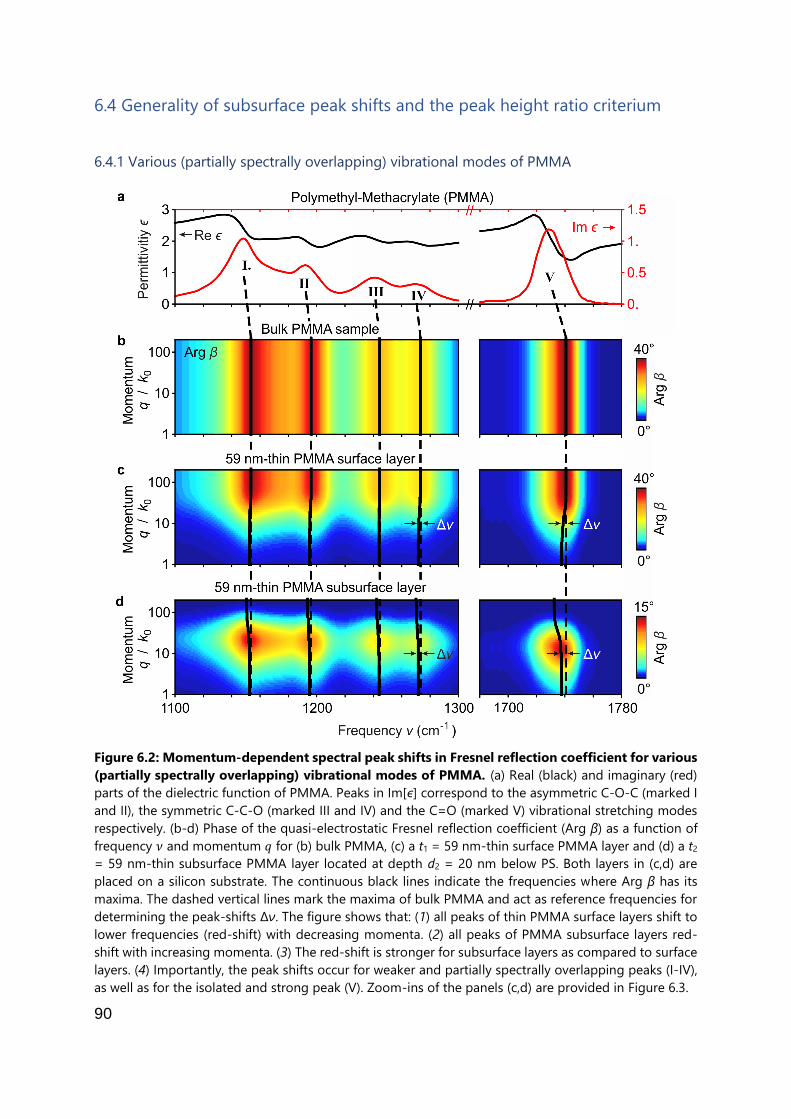
90
6.4 Generality of subsurface peak shifts and the peak height ratio criterium
6.4.1 Various (partially spectrally overlapping) vibrational modes of PMMA
Figure 6.2: Momentum-dependent spectral peak shifts in Fresnel reflection coefficient for various
(partially spectrally overlapping) vibrational modes of PMMA. (a) Real (black) and imaginary (red)
parts of the dielectric function of PMMA. Peaks in Im[ϵ] correspond to the asymmetric C-O-C (marked I
and II), the symmetric C-C-O (marked III and IV) and the C=O (marked V) vibrational stretching modes
respectively. (b-d) Phase of the quasi-electrostatic Fresnel reflection coefficient (Arg β) as a function of
frequency 𝜈 and momentum 𝑞 for (b) bulk PMMA, (c) a t1 = 59 nm-thin surface PMMA layer and (d) a t2
= 59 nm-thin subsurface PMMA layer located at depth d2 = 20 nm below PS. Both layers in (c,d) are
placed on a silicon substrate. The continuous black lines indicate the frequencies where Arg β has its
maxima. The dashed vertical lines mark the maxima of bulk PMMA and act as reference frequencies for
determining the peak-shifts Δν. The figure shows that: (1) all peaks of thin PMMA surface layers shift to
lower frequencies (red-shift) with decreasing momenta. (2) all peaks of PMMA subsurface layers red-
shift with increasing momenta. (3) The red-shift is stronger for subsurface layers as compared to surface
layers. (4) Importantly, the peak shifts occur for weaker and partially spectrally overlapping peaks (I-IV),
as well as for the isolated and strong peak (V). Zoom-ins of the panels (c,d) are provided in Figure 6.3.
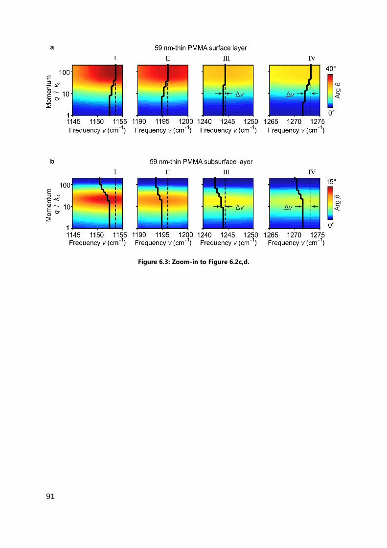
91
Figure 6.3: Zoom-in to Figure 6.2c,d.

92
Figure 6.4: Correlation of nano-FTIR peak characteristics for various (partially spectrally
overlapping) vibrational modes of PMMA. (a) Real (black) and imaginary (red) parts of the dielectric
function of PMMA. Peaks in Im[ϵ] correspond to the asymmetric C-O-C (marked I and II), the symmetric
C-C-O (marked III and IV) and the C=O (marked V) vibrational stretching modes respectively. (b)
Calculated spectral peak positions ν3max and (c) peak height ratios C of PMMA surface (black symbols)
and PMMA subsurface (red symbols) layers are plotted versus the corresponding peak heights φ3max, for
the vibrational modes I-IV of PMMA. Arrows indicate decreasing PMMA surface layer thickness t1 (black)
and increasing PMMA subsurface layer depth d2 (red). Subsurface PMMA layer thickness is t2 = 59 nm.
Green areas in (c) indicate the data spaces that correspond to subsurface material. The figure shows for
various (partially spectrally overlapping) vibrational modes of PMMA that: (1) nano-FTIR peak positions
shift to lower frequencies (red-shift) when the thickness t1 of a surface layer decreases or when the depth
d2 of a subsurface layer increases. (2) The red-shift is stronger for subsurface layers as compared to
surface layers. (3) Most interesting and important, the peak height ratios C = φ4max/φ
3max observed for all
molecular vibrations of PMMA behave nearly the same as that of the C=O peak (Figure 5.10), and thus
can be considered as a rather robust criterium for distinguishing surface and subsurface layers.

93
6.4.2 Differently strong vibrational modes of PEO
Figure 6.5: Momentum-dependent spectral peak shifts in Fresnel reflection coefficient for
differently strong vibrational modes of Polyethylene-oxide (PEO). (a) Real (black) and imaginary
(red) parts of the dielectric function of PEO. Peaks in Im[ϵ] (marked i-iii) correspond to C-O stretching
modes. (b-d) Phase of the quasi-electrostatic Fresnel reflection coefficient (Arg 𝛽) as a function of
frequency ν and momentum q for (b) bulk PEO, (c) a t1 = 59 nm-thin surface PEO layer and (d) a t2 = 59
nm-thin subsurface PEO layer located at depth d2 = 20 nm below PS. Both layers in (c,d) are placed on
a silicon substrate. The continuous black lines indicate the frequencies where Arg β has its maxima. The
dashed vertical lines mark the maxima of bulk PEO and act as reference frequencies for determining the
peak-shifts Δν. The figure shows (for other peaks than of PMMA) that: (1) peaks of thin PEO surface
layers shift to lower frequencies (red-shift) with decreasing momenta. (2) peaks of PEO subsurface layers
red-shift with increasing momenta. (3) The red-shift is stronger for subsurface layers as compared to
surface layers. (4) The magnitude of Δν largely varies from peak to peak and is not directly related to the
strength of a vibrational mode; i.e. the bonds i and iii are similar in Im[ϵ] but different in Δν, on the other
hand, the bonds ii and iii are similar in Δν but different in Im[ϵ].

94
Figure 6.6: Correlation of nano-FTIR peak characteristics for various (differently strong)
vibrational modes of PEO. (a) Real (black) and imaginary (red) parts of the dielectric function of PEO.
Peaks in Im[ϵ] (marked i-iii) correspond to C-O vibrational stretching modes. (b) Calculated spectral peak
positions ν3max and (c) peak height ratios C of PEO surface (black symbols) and PEO subsurface (red
symbols) layers are plotted versus the corresponding peak heights φ3max, for the vibrational modes i-iii
of PEO. Arrows indicate decreasing PEO surface layer thickness t1 (black) and increasing PEO subsurface
layer depth d2 (red). Subsurface PEO layer thicknesses are t2 = 15 nm (dotted red line), t2 = 59 nm (dashed
red line) and t2 = 100 nm (solid red line). Green areas in (c) indicate the data spaces that correspond to
subsurface material. The figure shows for differently strong vibrational modes of PEO that: (1) nano-FTIR
peak positions shift to lower frequencies (red-shift) when the thickness t1 of a surface layer decreases or
when the depth d2 of a subsurface layer increases. (2) The red-shift is stronger for subsurface layers as
compared to surface layers. (3) Most interesting and important, the peak height ratios C = φ4max/φ
3max
observed for all molecular vibrations of PEO behave nearly the same as that of the C=O peak of PMMA
(Figure 5.10), and thus can be considered as a rather robust criterium for distinguishing surface and
subsurface layers.

95
Figure 6.7: Comparison of experimental and calculated nano-FTIR peak characteristics for PEO. (a)
Experimental and (b) calculated nano-FTIR phase spectra of PEO surface layers with thickness t1
= { 25, 92 } nm (black symbols) and PEO subsurface layers with average thickness t2 = 34 nm and depth
d2 = { 19, 25, 34, 53 } nm (red symbols). (c) Spectral peak positions ν3max and (e) peak height ratios C for
the peak centered at 1115 cm-1
of PEO surface (black symbols) and PEO subsurface (red symbols) layers
are plotted versus the corresponding peak heights φ3max. Arrows indicate decreasing PEO surface layer
thickness t1 (black) and increasing PEO subsurface layer depth d2 (red). (d,f) Calculation results analogous
to Figure 5.10c and e. Additionally, results for a large range of PEO surface layer thicknesses t1 and PEO
subsurface layer depths d2 are shown. (e,f) Green areas indicate the data spaces that correspond to
subsurface material. (g-l) Data analogous to panels a-f, for the peak centered at 1150 cm-1. Spectral
resolution of the experiments 17 cm-1. The figure shows that (1) experimental and calculated nano-FTIR
peak positions of subsurface PEO layers shift to lower frequencies (red-shift) compared to that of surface
PEO layers of similar thickness. (2) The amount of the red-shift varies, depending on which peak is
analyzed. (3) Most interesting and important, the peak height ratios C = φ4max/φ
3max observed for all PEO
subsurface layers are smaller than those of PEO surface layers, corroborating their use as a rather robust
criterium for distinguishing surface and subsurface layers.

96
6.4.3 Lorentz oscillators with different high-frequency permittivity
Figure 6.8: Correlation of nano-FTIR peak characteristics for a model Lorentz oscillator with
varying high-frequency permittivities. (a) Real (black) and imaginary (red) parts of dielectric functions
modelled by Lorentz oscillators with different high-frequency permittivities ϵ∞ = { 3.2, 2.2, 1.7 } and fixed
ν0=1739 cm-1, γ = 26 cm-1, A0 = 240 cm-1. (b) Calculated spectral peak positions ν3max and (c) peak height
ratios C of surface (black symbols) and subsurface (red symbols) layers are plotted versus the
corresponding peak heights φ3max, for layers with the permittivities shown in panel a. Arrows indicate
decreasing surface layer thickness t1 (black) and increasing subsurface layer depth d2 (red). Subsurface
layer thicknesses are t2 = 15 nm (dotted red line), t2 = 59 nm (dashed red line) and t2 = 100 nm (solid
red line). Green areas in (c) indicate the data spaces that correspond to subsurface material. The figure
shows for vibrational modes modelled by Lorentz oscillators with different high-frequency permittivities
ϵ∞ that: (1) nano-FTIR peak positions shift to lower frequencies (red-shift) when the thickness t1 of a
surface layer decreases or when the depth d2 of a subsurface layer increases. (2) The red-shift is stronger
for subsurface layers as compared to surface layers. (3) Most interesting and important, the peak height
ratios C = φ4max/φ
3max observed for all modelled vibrations behave nearly the same as that of the C=O
peak of PMMA (Figure 5.10), and thus can be considered as a rather robust criterium for distinguishing
surface and subsurface layers.
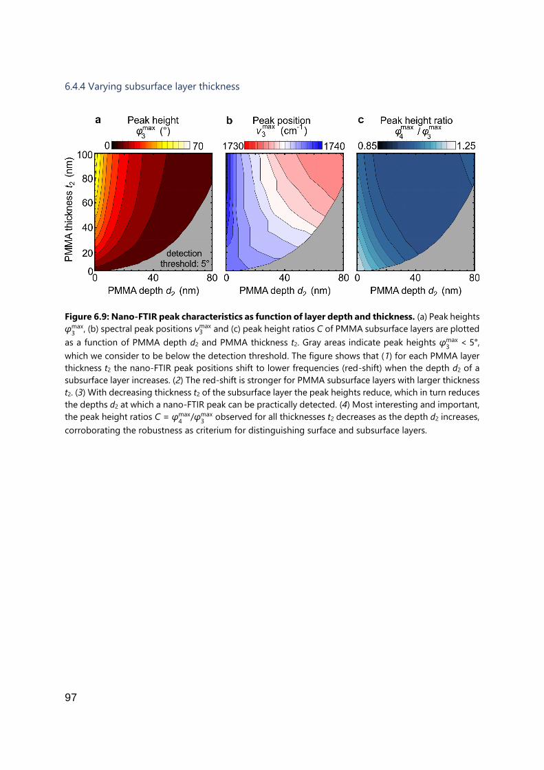
97
6.4.4 Varying subsurface layer thickness
Figure 6.9: Nano-FTIR peak characteristics as function of layer depth and thickness. (a) Peak heights
φ3max, (b) spectral peak positions ν3
max and (c) peak height ratios C of PMMA subsurface layers are plotted
as a function of PMMA depth d2 and PMMA thickness t2. Gray areas indicate peak heights φ3max < 5°,
which we consider to be below the detection threshold. The figure shows that (1) for each PMMA layer
thickness t2 the nano-FTIR peak positions shift to lower frequencies (red-shift) when the depth d2 of a
subsurface layer increases. (2) The red-shift is stronger for PMMA subsurface layers with larger thickness
t2. (3) With decreasing thickness t2 of the subsurface layer the peak heights reduce, which in turn reduces
the depths d2 at which a nano-FTIR peak can be practically detected. (4) Most interesting and important,
the peak height ratios C = φ4max/φ
3max observed for all thicknesses t2 decreases as the depth d2 increases,
corroborating the robustness as criterium for distinguishing surface and subsurface layers.
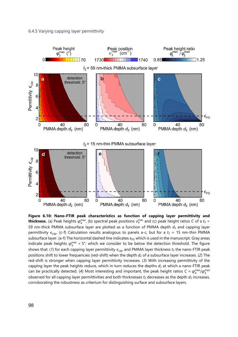
98
6.4.5 Varying capping layer permittivity
Figure 6.10: Nano-FTIR peak characteristics as function of capping layer permittivity and
thickness. (a) Peak heights φ4max, (b) spectral peak positions ν4
max and (c) peak height ratios C of a t2 =
59 nm-thick PMMA subsurface layer are plotted as a function of PMMA depth d2 and capping layer
permittivity ϵcap. (c-f) Calculation results analogous to panels a-c, but for a t2 = 15 nm-thin PMMA
subsurface layer. (a-f) The horizontal dashed line indicates ϵPS which is used in the manuscript. Gray areas
indicate peak heights φ4max < 5°, which we consider to be below the detection threshold. The figure
shows that: (1) for each capping layer permittivity ϵcap and PMMA layer thickness t2 the nano-FTIR peak
positions shift to lower frequencies (red-shift) when the depth d2 of a subsurface layer increases. (2) The
red-shift is stronger when capping layer permittivity increases. (3) With increasing permittivity of the
capping layer the peak heights reduce, which in turn reduces the depths d2 at which a nano-FTIR peak
can be practically detected. (4) Most interesting and important, the peak height ratios C = φ4max/φ
3max
observed for all capping layer permittivities and both thicknesses t2 decreases as the depth d2 increases,
corroborating the robustness as criterium for distinguishing surface and subsurface layers.

99

100
7 References
1. Zayats, A. V. & Richards (Prof.), D. Nano-optics and Near-field Optical Microscopy. (Artech House, 2009). 2. Keilmann, F. & Hillenbrand, R. Near-field microscopy by elastic light scattering from a tip. Phil. Trans. R. Soc. Lond. A 362, 787–805 (2004). 3. Zenhausern, F., O’Boyle, M. P. & Wickramasinghe, H. K. Apertureless near-field optical microscope. Applied Physics Letters 65, 1623–1625 (1994). 4. Markus B Raschke & Christoph Lienau. Apertureless near-field optical microscopy: Tip-sample coupling in elastic light scattering. Applied Physics Letters 83, 5089–5091 (2003). 5. Taubner, T., Hillenbrand, R. & Keilmann, F. Performance of visible and mid-infrared scattering-type near-field optical microscopes. Journal of Microscopy 210, 311–314 (2003). 6. Keilmann, F., Huber, A. J. & Hillenbrand, R. Nanoscale Conductivity Contrast by Scattering-Type Near-Field Optical Microscopy in the Visible, Infrared and THz Domains. Journal of Infrared, Millimeter, and Terahertz Waves, Volume 30, Issue 12, pp.1255-1268 30, 1255–1268 (2009). 7. Raschke, M. B. et al. Apertureless Near-Field Vibrational Imaging of Block-Copolymer Nanostructures with Ultrahigh Spatial Resolution. ChemPhysChem 6, 2197–2203 (2005). 8. Chen, H.-T., Kersting, R. & Cho, G. C. Terahertz imaging with nanometer resolution. Appl. Phys. Lett. 83, 3009–3011 (2003). 9. Cho, G. C., Chen, H.-T., Kraatz, S., Karpowicz, N. & Kersting, R. Apertureless terahertz near-field microscopy. Semicond. Sci. Technol. 20, S286–S292 (2005). 10. Novotny, L. & Hecht, B. Principles of Nano-Optics. (Cambridge, 2006). 11. Behr, N. & Raschke, M. B. Optical Antenna Properties of Scanning Probe Tips: Plasmonic Light Scattering, Tip-Sample Coupling, and Near-Field Enhancement. J. Phys. Chem. C 112, 3766–3773 (2008). 12. Ocelic, N., Huber, A. & Hillenbrand, R. Pseudoheterodyne detection for background-free near-field spectroscopy. Applied Physics Letters 89, 101124 (2006). 13. Ocelic, N. Quantitative near-field phonon-polariton spectroscopy. (Technische Universität München, 2007). 14. Griffiths, P. R. & de Haseth, J. A. Fourier Transform Infrared Spectroscopy. (John Wiley & Sons, Inc., 2007).

101
15. Huth, F. et al. Nano-FTIR Absorption Spectroscopy of Molecular Fingerprints at 20nm Spatial Resolution. Nano Lett. 12, 3973–3978 (2012). 16. Amarie, S., Ganz, T. & Keilmann, F. Mid-infrared near-field spectroscopy. Opt. Express, OE 17, 21794–21801 (2009). 17. Huth, F., Schnell, M., Wittborn, J., Ocelic, N. & Hillenbrand, R. Infrared-spectroscopic nanoimaging with a thermal source. Nat Mater 10, 352–356 (2011). 18. Mastel, S., Govyadinov, A. A., de Oliveira, T. V. A. G., Amenabar, I. & Hillenbrand, R. Nanoscale-resolved chemical identification of thin organic films using infrared near-field spectroscopy and standard Fourier transform infrared references. Appl. Phys. Lett. 106, 023113 (2015). 19. Taubner, T., Keilmann, F. & Hillenbrand, R. Nanoscale-resolved subsurface imaging by scattering-type near-field optical microscopy. Optics Express 13, 8893 (2005). 20. Krutokhvostov, R. et al. Enhanced resolution in subsurface near-field optical microscopy. Optics Express 20, 593 (2012). 21. Engelhardt, A. P., Hauer, B. & Taubner, T. Visibility of weak contrasts in subsurface scattering near-field microscopy. Ultramicroscopy 126, 40–43 (2013). 22. Mester, L., Govyadinov, A. A., Chen, S., Goikoetxea, M. & Hillenbrand, R. Subsurface chemical nanoidentification by nano-FTIR spectroscopy. Nature Communications 11, 3359 (2020). 23. Govyadinov, A. A. et al. Recovery of Permittivity and Depth from Near-Field Data as a Step toward Infrared Nanotomography. ACS Nano 8, 6911–6921 (2014). 24. Lewin, M. et al. Imaging of phase change materials below a capping layer using correlative infrared near-field microscopy and electron microscopy. Appl. Phys. Lett. 107, 151902 (2015). 25. Moon, K. et al. Subsurface Nanoimaging by Broadband Terahertz Pulse Near-Field Microscopy. Nano Lett. 15, 549–552 (2015). 26. Gozar, A., Litombe, N. E., Hoffman, J. E. & Božović, I. Optical Nanoscopy of High Tc Cuprate Nanoconstriction Devices Patterned by Helium Ion Beams. Nano Lett. 17, 1582–1586 (2017). 27. Mooshammer, F. et al. Nanoscale Near-Field Tomography of Surface States on (Bi0.5Sb0.5)2Te3. Nano Lett. 18, 7515–7523 (2018). 28. Jung, L. et al. Exploring the detection limits of infrared near-field microscopy regarding small buried structures and pushing them by exploiting superlens-related effects. Opt. Express, OE 24, 4431–4441 (2016).

102
29. Huber, A. J., Keilmann, F., Wittborn, J., Aizpurua, J. & Hillenbrand, R. Terahertz Near-Field Nanoscopy of Mobile Carriers in Single Semiconductor Nanodevices. Nano Lett. 8, 3766–3770 (2008). 30. Autore, M., Mester, L., Goikoetxea, M. & Hillenbrand, R. Substrate Matters: Surface-Polariton Enhanced Infrared Nanospectroscopy of Molecular Vibrations. Nano Lett. 19, 8066–8073 (2019). 31. Mertz, J. Introduction to optical microscopy. (Roberts and Company Publishers, 2016). 32. Born, M. & Wolf, E. Principles of Optics. (Cambridge University Press, 1999). 33. Electromagnetic spectrum. Encyclopaedia Britannica https://www.britannica.com/science/electromagnetic-spectrum (2019). 34. Schrader, B. Infrared and Raman spectroscopy. (VCH Verlagsgesellschaft GmbH, 1995). 35. Mark Fox. Optical Properties of Solids. (Oxford University Press, 2010). 36. Abbe, E. Beiträge zur Theorie des Mikroskops und der mikroskopischen Wahrnehmung. Archiv f. mikrosk. Anatomie 9, 413–418 (1873). 37. Guozhong, C. Nanostructures and Nanomaterials: Synthesis, Properties and Applications. (World Scientific Publishing, 2004). 38. Mayer, E., Hug, H. J. & Bennewitz, R. Scanning Probe Microscopy: The Lab on a Tip. vol. 1+2 (Wiley-VCH, 2012). 39. Ocelic, N. & Hillenbrand, R. Subwavelength-scale tailoring of surface phonon polaritons by focused ion-beam implantation. Nat Mater 3, 606–609 (2004). 40. Huth, F. Nano-FTIR - Nanoscale Infrared Near-field Spectroscopy. (Universidad del Pais Vasco, 2015). 41. Lu, F., Jin, M. & Belkin, M. A. Tip-enhanced infrared nanospectroscopy via molecular expansion force detection. Nature Photonics 8, 307–312 (2014). 42. Dazzi, A. et al. AFM–IR: Combining Atomic Force Microscopy and Infrared Spectroscopy for Nanoscale Chemical Characterization. Appl Spectrosc 66, 1365–1384 (2012). 43. Rajapaksa, I., Uenal, K. & Wickramasinghe, H. K. Image force microscopy of molecular resonance: A microscope principle. Applied Physics Letters 97, 073121 (2010).

103
44. Nowak, D. et al. Nanoscale chemical imaging by photoinduced force microscopy. Sci Adv 2, (2016). 45. Greffet, J.-J. & Carminati, R. Image formation in near-field optics. Progress in Surface Science 56, 133–237 (1997). 46. Michelson, A. A. XXXVIII. On the application of interference-methods to spectroscopic measurements.—I. The London, Edinburgh, and Dublin Philosophical Magazine and Journal of Science 31, 338–346 (1891). 47. Keilmann, F. & Hillenbrand, R. Nano-Optics and Near-Field Optical Microscopy. (Artech House, 2008). 48. A Cvitkovic, N Ocelic & R Hillenbrand. Analytical model for quantitative prediction of material contrasts in scattering-type near-field optical microscopy. Optics Express 15, 8550–8565 (2007). 49. Taubner, T., Hillenbrand, R. & Keilmann, F. Nanoscale polymer recognition by spectral signature in scattering infrared near-field microscopy. Applied Physics Letters 85, 5064–5066 (2004). 50. Hillenbrand, R., Taubner, T. & Keilmann, F. Phonon-enhanced light–matter interaction at the nanometre scale. Nature 418, 159–162 (2002). 51. Aizpurua, J., Taubner, T., Javier Garcia de Abajo, F., Brehm, M. & Hillenbrand, R. Substrate-enhanced infrared near-field spectroscopy. Optics Express 16, 1529–1545 (2008). 52. Govyadinov, A. A., Amenabar, I., Huth, F., Carney, P. S. & Hillenbrand, R. Quantitative Measurement of Local Infrared Absorption and Dielectric Function with Tip-Enhanced Near-Field Microscopy. J. Phys. Chem. Lett. 4, 1526–1531 (2013). 53. Lewin, M. et al. Sb2Te3 Growth Study Reveals That Formation of Nanoscale Charge Carrier Domains Is an Intrinsic Feature Relevant for Electronic Applications. ACS Appl. Nano Mater. 1, 6834–6842 (2018). 54. Hauer, B., Engelhardt, A. P. & Taubner, T. Quasi-analytical model for scattering infrared near-field microscopy on layered systems. Optics Express 20, 13173 (2012). 55. Caldwell, J. D. et al. Low-loss, infrared and terahertz nanophotonics using surface phonon polaritons. Nanophotonics 4, 44–68 (2015). 56. Huber, A. j., Ocelic, N. & Hillenbrand, R. Local excitation and interference of surface phonon polaritons studied by near-field infrared microscopy. Journal of Microscopy 229, 389–395 (2008). 57. Jackson, J. D. Classical Electrodynamics. (John Wiley & Sons, Inc., 2001).

104
58. McLeod, A. S. et al. Model for quantitative tip-enhanced spectroscopy and the extraction of nanoscale-resolved optical constants. Phys. Rev. B 90, 085136 (2014). 59. Jiang, B.-Y., Zhang, L. M., Castro Neto, A. H., Basov, D. N. & Fogler, M. M. Generalized spectral method for near-field optical microscopy. Journal of Applied Physics 119, 054305 (2016). 60. Brehm, M. Infrarot-Mikrospektroskopie mit einem Nahfeldmikroskop. (Technische Universität München, 2006). 61. Wang, B. & Woo, C. H. Atomic force microscopy-induced electric field in ferroelectric thin films. Journal of Applied Physics 94, 4053–4059 (2003). 62. Hauer, B. Nano-optical mapping of permittivity contrasts and electronic properties at the surface and beneath. (RWTH Aachen University, 2015). 63. Chen, S. et al. On the anomalous optical conductivity dispersion of electrically conducting polymers: ultra-wide spectral range ellipsometry combined with a Drude–Lorentz model. Journal of Materials Chemistry C 7, 4350–4362 (2019). 64. Liu, Y. et al. Negative group velocity of surface plasmons on thin metallic films. in Plasmonics: Metallic Nanostructures and their Optical Properties IV vol. 6323 63231M (International Society for Optics and Photonics, 2006). 65. Chen, X. et al. Modern Scattering-Type Scanning Near-Field Optical Microscopy for Advanced Material Research. Advanced Materials 31, 1804774 (2019). 66. Fei, Z. et al. Infrared Nanoscopy of Dirac Plasmons at the Graphene–SiO2 Interface. Nano Lett. 11, 4701–4705 (2011). 67. Amenabar Altuna, I. Infrared nanospectroscopy and hyperspectral nanoimaging of organic matter. (Universidad del Pais Vasco, 2017). 68. Li, M., Cushing, S. K. & Wu, N. Plasmon-Enhanced Optical Sensors: A Review. Analyst 140, 386–406 (2015). 69. Zhang, L. M. et al. Near-field spectroscopy of silicon dioxide thin films. Phys. Rev. B 85, 075419 (2012). 70. Luo, W. et al. High sensitivity variable-temperature infrared nanoscopy of conducting oxide interfaces. Nature Communications 10, 2774 (2019). 71. Maissen, C., Chen, S., Nikulina, E., Govyadinov, A. & Hillenbrand, R. Probes for Ultrasensitive THz Nanoscopy. ACS Photonics 6, 1279–1288 (2019). 72. Knoll, B. & Keilmann, F. Enhanced dielectric contrast in scattering-type scanning near-field optical microscopy. Optics Communications 182, 321–328 (2000).

105
73. Amarie, S. et al. Nano-FTIR chemical mapping of minerals in biological materials. Beilstein J Nanotechnol 3, 312–323 (2012). 74. Binnig, G., Quate, C. F. & Gerber, Ch. Atomic Force Microscope. Phys. Rev. Lett. 56, 930–933 (1986). 75. Eaton, P. & West, P. Atomic Force Microscopy. (Oxford University Press, 2010). 76. Berlin, A. A., Kablov, V. F., Pimerzin, A. A. & Zlotsky, S. S. Key Elements in POLYMERS for ENGINEERS and CHEMISTS: From Data to Applications. (Apple Academic Press, 2014). 77. Bechtel, H. A., Muller, E. A., Olmon, R. L., Martin, M. C. & Raschke, M. B. Ultrabroadband infrared nanospectroscopic imaging. PNAS 111, 7191–7196 (2014). 78. Westermeier, C. et al. Sub-micron phase coexistence in small-molecule organic thin films revealed by infrared nano-imaging. Nat Commun 5, 1–6 (2014). 79. Qazilbash, M. M. et al. Mott Transition in VO2 Revealed by Infrared Spectroscopy and Nano-Imaging. Science 318, 1750–1753 (2007). 80. Stiegler, J. M. et al. Nanoscale Free-Carrier Profiling of Individual Semiconductor Nanowires by Infrared Near-Field Nanoscopy. Nano Lett. 10, 1387–1392 (2010). 81. Lucas, I. T. et al. IR Near-Field Spectroscopy and Imaging of Single LixFePO4 Microcrystals. Nano Lett. 15, 1–7 (2015). 82. Ritchie, E. T. et al. Mapping Free-Carriers in Multijunction Silicon Nanowires Using Infrared Near-Field Optical Microscopy. Nano Lett. 17, 6591–6597 (2017). 83. Sterl, F. et al. Nanoscale Hydrogenography on Single Magnesium Nanoparticles. Nano Lett. 18, 4293–4302 (2018). 84. Amenabar, I. et al. Structural analysis and mapping of individual protein complexes by infrared nanospectroscopy. Nat Commun 4, 1–9 (2013). 85. Xu, X. G., Rang, M., Craig, I. M. & Raschke, M. B. Pushing the Sample-Size Limit of Infrared Vibrational Nanospectroscopy: From Monolayer toward Single Molecule Sensitivity. J. Phys. Chem. Lett. 3, 1836–1841 (2012). 86. Berweger, S. et al. Nano-Chemical Infrared Imaging of Membrane Proteins in Lipid Bilayers. J. Am. Chem. Soc. 135, 18292–18295 (2013). 87. Cvitkovic, A., Ocelic, N., Aizpurua, J., Guckenberger, R. & Hillenbrand, R. Infrared Imaging of Single Nanoparticles via Strong Field Enhancement in a Scanning Nanogap. Phys. Rev. Lett. (2006) doi:10.1103/PhysRevLett.97.060801.

106
88. Brehm, M., Taubner, T., Hillenbrand, R. & Keilmann, F. Infrared spectroscopic mapping of single nanoparticles and viruses at nanoscale resolution. Nano Letters 6, 1307–1310 (2006). 89. Cvitkovic, A., Ocelic, N. & Hillenbrand, R. Material-Specific Infrared Recognition of Single Sub-10 nm Particles by Substrate-Enhanced Scattering-Type Near-Field Microscopy. Nano Lett. 7, 3177–3181 (2007). 90. Steidtner, J. & Pettinger, B. Tip-Enhanced Raman Spectroscopy and Microscopy on Single Dye Molecules with 15 nm Resolution. Phys. Rev. Lett. 100, 236101 (2008). 91. Hoffmann, J. M., Hauer, B. & Taubner, T. Antenna-enhanced infrared near-field nanospectroscopy of a polymer. Applied Physics Letters 101, 193105 (2012). 92. Muller, E. A. et al. Nanoimaging and Control of Molecular Vibrations through Electromagnetically Induced Scattering Reaching the Strong Coupling Regime. ACS Photonics 5, 3594–3600 (2018). 93. O’Callahan, B. T., Hentschel, M., Raschke, M. B., El-Khoury, P. Z. & Lea, A. S. Ultrasensitive Tip- and Antenna-Enhanced Infrared Nanoscopy of Protein Complexes. J. Phys. Chem. C 123, 17505–17509 (2019). 94. Hu, H. et al. Far-field nanoscale infrared spectroscopy of vibrational fingerprints of molecules with graphene plasmons. Nature Communications 7, 12334 (2016). 95. Bass, M. et al. Handbook of Optics: Optical Properties of Materials, Nonlinear Optics, Quantum Optics. vol. 3rd (McGraw-Hill Education, 2009). 96. Amarie, S. & Keilmann, F. Broadband-infrared assessment of phonon resonance in scattering-type near-field microscopy. Phys. Rev. B 83, 045404 (2011). 97. Li, P. et al. Reversible optical switching of highly confined phonon–polaritons with an ultrathin phase-change material. Nature Materials 15, 870–875 (2016). 98. Kuzmenko, A. B. Kramers–Kronig constrained variational analysis of optical spectra. Review of Scientific Instruments 76, 083108 (2005). 99. Neubrech, F. et al. Resonant Plasmonic and Vibrational Coupling in a Tailored Nanoantenna for Infrared Detection. Phys. Rev. Lett. 101, 157403 (2008). 100. Neubrech, F., Huck, C., Weber, K., Pucci, A. & Giessen, H. Surface-Enhanced Infrared Spectroscopy Using Resonant Nanoantennas. Chem. Rev. 117, 5110–5145 (2017). 101. Autore, M. et al. Boron nitride nanoresonators for phonon-enhanced molecular vibrational spectroscopy at the strong coupling limit. Light: Science & Applications 7, 17172–17172 (2018).

107
102. Taubner, T., Keilmann, F. & Hillenbrand, R. Nanomechanical Resonance Tuning and Phase Effects in Optical Near-Field Interaction. Nano Lett. 4, 1669–1672 (2004). 103. Wang, H., Wang, L., Jakob, D. S. & Xu, X. G. Tomographic and multimodal scattering-type scanning near-field optical microscopy with peak force tapping mode. Nature Communications 9, 2005 (2018). 104. Huber, A., Ocelic, N., Kazantsev, D. & Hillenbrand, R. Near-field imaging of mid-infrared surface phonon polariton propagation. Appl. Phys. Lett. 87, 081103 (2005). 105. Sumikura, H. et al. Highly Confined and Switchable Mid-Infrared Surface Phonon Polariton Resonances of Planar Circular Cavities with a Phase Change Material. Nano Lett. 19, 2549–2554 (2019). 106. Dubrovkin, A. M., Qiang, B., Krishnamoorthy, H. N. S., Zheludev, N. I. & Wang, Q. J. Ultra-confined surface phonon polaritons in molecular layers of van der Waals dielectrics. Nature Communications 9, 1762 (2018). 107. Law, S., Yu, L., Rosenberg, A. & Wasserman, D. All-Semiconductor Plasmonic Nanoantennas for Infrared Sensing. Nano Lett. 13, 4569–4574 (2013). 108. Wagner, M. et al. Ultrafast Dynamics of Surface Plasmons in InAs by Time-Resolved Infrared Nanospectroscopy. Nano Lett. 14, 4529–4534 (2014). 109. Barho, F. B. et al. Highly doped semiconductor plasmonic nanoantenna arrays for polarization selective broadband surface-enhanced infrared absorption spectroscopy of vanillin. Nanophotonics 7, 507–516 (2017). 110. Zhou, Y. et al. Tunable Low Loss 1D Surface Plasmons in InAs Nanowires. Advanced Materials 30, 1802551 (2018). 111. Dai, S. et al. Tunable Phonon Polaritons in Atomically Thin van der Waals Crystals of Boron Nitride. Science 343, 1125–1129 (2014). 112. Li, P. et al. Optical Nanoimaging of Hyperbolic Surface Polaritons at the Edges of van der Waals Materials. Nano Lett. 17, 228–235 (2017). 113. Chen, J. et al. Optical nano-imaging of gate-tunable graphene plasmons. Nature 487, 77–81 (2012). 114. Fei, Z. et al. Gate-tuning of graphene plasmons revealed by infrared nano-imaging. Nature 487, 82–85 (2012). 115. Huber, A. J., Deutsch, B., Novotny, L. & Hillenbrand, R. Focusing of surface phonon polaritons. Appl. Phys. Lett. 92, 203104 (2008). 116. Alonso-González, P. et al. Controlling graphene plasmons with resonant metal antennas and spatial conductivity patterns. Science 344, 1369–1373 (2014).

108
117. Dai, S. et al. Subdiffractional focusing and guiding of polaritonic rays in a natural hyperbolic material. Nature Communications 6, 6963 (2015). 118. Li, P. et al. Hyperbolic phonon-polaritons in boron nitride for near-field optical imaging and focusing. Nature Communications 6, 7507 (2015). 119. Kästner, B. et al. Infrared Nanospectroscopy of Phospholipid and Surfactin Monolayer Domains. ACS Omega 3, 4141–4147 (2018). 120. Caldwell, J. D. et al. Low-Loss, Extreme Subdiffraction Photon Confinement via Silicon Carbide Localized Surface Phonon Polariton Resonators. Nano Lett. 13, 3690–3697 (2013). 121. Wang, T. et al. Phonon-Polaritonic Bowtie Nanoantennas: Controlling Infrared Thermal Radiation at the Nanoscale. ACS Photonics 4, 1753–1760 (2017). 122. Alfaro-Mozaz, F. J. et al. Nanoimaging of resonating hyperbolic polaritons in linear boron nitride antennas. Nature Communications 8, 15624 (2017). 123. Ho, K. et al. Nanoscale Subsurface Morphologies in Block Copolymer Thin Films Revealed by Combined Near-Field Infrared Microscopy and Mechanical Mapping. ACS Appl. Polym. Mater. 1, 933–938 (2019). 124. Pollard, B., Muller, E. A., Hinrichs, K. & Raschke, M. B. Vibrational nano-spectroscopic imaging correlating structure with intermolecular coupling and dynamics. Nature Communications 5, 3587 (2014). 125. Pacansky, J., England, C. & Waltman, R. J. Complex refractive indexes for polymers over the infrared spectral region: Specular reflection IR spectra of polymers. Journal of Polymer Science Part B: Polymer Physics 25, 901–933 (1987). 126. Arnulf Röseler. Infrared Spectroscopic Ellipsometry. (Akademie-Verlag, 1990). 127. Orlov, A. S., Kiselev, S. A., Kiseleva, E. A., Budeeva, A. V. & Mashukov, V. I. Determination of styrene-butadiene rubber composition by attenuated total internal reflection infrared spectroscopy. JApSp 80, 47–53 (2013). 128. Schmidt, U., Hild, S., Ibach, W. & Hollricher, O. Characterization of Thin Polymer Films on the Nanometer Scale with Confocal Raman AFM. Macromolecular Symposia 230, 133–143 (2005). 129. James, J., Thomas, G. V., P, P. K., Kalarikkal, N. & Thomas, S. Thermoplastic–elastomer composition based on an interpenetrating polymeric network of styrene butadiene rubber–poly(methyl methacrylate) as an efficient vibrational damper. New J. Chem. 42, 1939–1951 (2018). 130. Ennis, D., Betz, H. & Ade, H. Direct spincasting of polystyrene thin films onto poly(methyl methacrylate). J. Polym. Sci. B Polym. Phys. 44, 3234–3244 (2006).

109
131. Olmos, D., Martín, E. V. & González-Benito, J. New molecular-scale information on polystyrene dynamics in PS and PS–BaTiO3 composites from FTIR spectroscopy. Phys. Chem. Chem. Phys. 16, 24339–24349 (2014). 132. Amma, S., Luo, J., Pantano, C. G. & Kim, S. H. Specular reflectance (SR) and attenuated total reflectance (ATR) infrared (IR) spectroscopy of transparent flat glass surfaces: A case study for soda lime float glass. Journal of Non-Crystalline Solids 428, 189–196 (2015). 133. Nolting. Grundkurs theoretische Physik. Bd.3: Elektrodynamik. vol. 3.

110
8 Own publications
This thesis is based on the following publications:
- Autore, M., Mester, L., Goikoetxea, M. & Hillenbrand, R. Substrate Matters: Surface-
Polariton Enhanced Infrared Nanospectroscopy of Molecular Vibrations. Nano Lett. 19,
8066–8073 (2019).
- Mester, L., Govyadinov, A. A., Chen, S., Goikoetxea, M. & Hillenbrand, R. Subsurface
chemical nanoidentification by nano-FTIR spectroscopy. Nature Comm. 11, 3359 (2020).

111
9 Acknowledgements
I want to express my gratitude to my supervisor Prof. Rainer Hillenbrand, group leader of the
nano-optics group at CIC nanoGUNE, for giving me the opportunity to join his group, always
being open for discussions and for his patience.
I thank Prof. Txema Pitarke, director of CIC nanoGUNE, for giving me the opportunity to
perform outstanding nanoscience research in the Basque Country at CIC nanoGUNE.
I am thankful to all present and past members of the nano-optics group at CIC nanoGUNE, for
a great atmosphere, interesting discussions, and mutual support. Special thanks to Monika
Goikoetxea, for always offering her help and support particularly related to the chemistry of
polymers. Many thanks also to Carlos Crespo (for taking good care of our laboratories and
helping out all group members wherever possible, starting already on day one with helping
through the Spanish bureaucracy), to Stefan Mastel and Iban Amenabar (for always being ready
to discuss details on the instrumentation of our laboratories), to Divya Virmani (for the 16
o’clock coffee breaks) and to Carlos Maciel and Irene Dolado (particularly for their help in
translating, but also for the scientific collaboration).
I also want to thank all collaborators and all members of the SPM2.0 network, for many
scientific discussions and contributions to many interesting projects.
I thank all employees of neaspec GmbH for their continuous technical support during the time
of my PhD thesis.
I further thank everyone involved in our interdisciplinary Tuesday, Thursday or Friday PhD-
reunions.
Special thanks go to my family and friends for their continuous support and a good time
throughout the whole thesis.
This work has received funding from the European Union’s Horizon 2020 research and
innovation program under the Marie Sklodowska-Curie grant agreement No. 721874 (SPM2.0).
I further acknowledge the financial support of my co-authors from the Spanish Ministry of
Science, Innovation and Universities (national project RTI2018-094830-B-100 and the project
MDM-2016-0618 of the Marie de Maeztu Units of Excellence Program) and the Basque
Government (grant No. IT1164-19).

112
10 Documentation