Socialization, Sexuality, and Innocence in The Catcher ... - Trepo
Upload
khangminh22Category
view
0download
0
SUBARNA BHATTARAI
CONDUCTING POLYMERS IN AUGMENTING THE PROPERTIES OF
BIOPOTENTIAL ELECTRODES
Master of Science Thesis
Examiners: Professor Jari Hyttinen and Minna
Kellomäki
Examiners and topic approved by the Dean of the
Faculty of Computing and Electrical Engineering
on 26th April 2017.

i
ABSTRACT
SUBARNA BHATTARAI: Conducting Polymers in Augmenting the Properties of
Biopotential Electrodes
Tampere University of Technology
Master of Science Thesis, 74 pages, 1 Appendix page
March 2017
Master’s Degree Programme in Electrical Engineering, MSc (Tech)
Major: Medical Instrumentation
Examiner: Professor Jari Hyttinen and Minna Kellomäki
Keywords: Polypyrrole, biopotential electrodes, electrode-electrolyte interface,
impedance magnitude and phase, morphology
Conducting polymers, especially Polypyrrole (PPy), have been extensively used for the
modification of the electrode surface by electrochemical deposition. The combination of
carbon nanotubes (CNTs) and PPy has also been successfully electrodeposited on the
electrode surface to lower the impedance. The morphology of such coated electrode
were also found to be rougher than PPy or CNT alone which could indicate greater
electroactive area of the coated film.
The thesis is based on electrodeposition of two types of biopotential electrodes: a)
Microelectrode arrays (MEAs) and b) Macroelectrodes. The electrodeposition process
was evaluated by chronopotentiometric measurement by measuring the charge and
current density.
The PPy and PPy/CNT solutions were successfully electrodeposited onto the
Platinum(Pt) macroelectrode surface. PPy/CNT decreased the macroelectrode
impedance. Optical Profilometer analysis showed that PPy-CNT 0.25 sample (made
from 0.25mg/ml of CNT) produced the roughest surface and PPy-Control sample
produced the smoothest surface. Atomic Force Microscopy(AFM) analysis showed that
the PPy-CNT 0.5 sample (made from 0.5mg/ml of CNT) was more rougher than the
PPy surface. Micrograph analysis showed thick coating with PPy-CNT 0.25 and PPy-
CNT 0.5 samples than PPy-Control and PPy-CNT 0.1 (made from 0.1mg/ml of CNT)
samples.
A wide range of electrical properties were also observed in different frequencies. PPy-
CNT 0.5 was highly resistive at 1kHz with phase angle of 29° and most capacitive at
1.0Hz with phase angle of -68°compared to coated electrodes. PPy-CNT 0.25 showed
maximum impedance magnitude at 1.0Hz and PPy-CNT 0.5 showed least magnitude at
1KHz. Bare Pt was highly capacitive at 1Hz with the phase angle of -78°. PPy-CNT 0.5
was highly capacitive at lower frequencies (<100Hz) than any other coated electrodes
while PPy-CNT 0.25 was most resistive.
Plasma treatment reduced the MEAs impedance. However, the MEA was not coated
with PPy solution. Variations in charge and current densities was observed with MEAs
electrodeposition. These types of electrodeposition analysis could be useful in future
research to characterize the impedance of the coated film to improve the performance of
biopotential electrodes.

ii
PREFACE
I would like to thank my professors Jari Hyttinen and Minna Kellomäki for their
support and guidance throughout my thesis work.
I would like to thank my supervisor, MSc.Virpi Alarautalahti, for her immense support
and help. I would like to thank Sister Richards for her inspiration, love and support that
she has given me to write this project.
I would like to thank my family and friends for trusting me.
Tampere, 21.3.2017
Subarna Bhattarai

iii
CONTENTS
1 INTRODUCTION ..................................................................................................... 1
2 THEORETICAL BACKGROUND ........................................................................... 3
2.1 Conducting polymers ......................................................................................... 3
2.1.1 Doping structures of conducting polymers ................................................. 4
2.1.2 Charge carriers in conducting polymers ..................................................... 5
2.1.3 Doping characteristics ................................................................................. 6
2.1.4 Application of CPs ...................................................................................... 8
2.1.5 Polypyrrole .................................................................................................. 9
2.2 Carbon nanotubes (CNTs) ................................................................................ 10
2.3 Biopotential electrodes ..................................................................................... 10
2.3.1 Electrode-electrolyte interface .................................................................. 11
2.3.2 Electrical characteristics............................................................................ 13
2.3.3 General requirements of the electrode material ........................................ 14
2.3.4 Safe charge injection limit and stimulation protocol ................................ 15
2.3.5 Charge vs charge density relationship....................................................... 16
3 MATERIALS AND METHODS............................................................................. 18
3.1 Material and solution preparation ..................................................................... 18
3.2 Polymerization .................................................................................................. 19
3.3 Impedance measurement .................................................................................. 20
3.3.1 Macroelectrode impedance measurement ................................................. 21
3.4 Imaging device ................................................................................................. 22
3.4.1 Optical Profilometer .................................................................................. 22
3.4.2 Atomic Force Microscopy (AFM) ............................................................ 24
3.4.3 Optical Microscope ................................................................................... 26
4 RESULTS ................................................................................................................ 27
4.1 MACROELECTRODES .................................................................................. 27
4.1.1 Macroelectrode electrodeposition ............................................................. 27
4.1.2 Electrical Impedance Spectroscopy .......................................................... 28
iv
4.1.3 Impedance measurement at frequencies of 1Hz and 1kHz ....................... 35
4.1.4 Average measurement at 1.0Hz and 1.0kHz ............................................. 37
4.1.5 Surface characterization ............................................................................ 40
4.2 MEA ................................................................................................................. 43
4.2.1 Electrodeposition....................................................................................... 44
4.2.2 Impedance measurements ......................................................................... 50
4.2.3 Micrograph Imaging.................................................................................. 55
5 DISCUSSION AND CONCLUSIONS ................................................................... 56
6 APPENDIX .............................................................................................................. 58
7 REFERENCES ........................................................................................................ 59

v
LIST OF FIGURES
Figure 1: Main chain structures of several representative conjugated polymers (Li
2015). ................................................................................................................................ 3
Figure 2: Isomers of polyacteylene a) cis-polyacteylene and b) trans-polyacetylene
(Goh et al. 2009). .............................................................................................................. 4
Figure 3: p-Doped structure of conducting PPy (Li 2015)............................................... 4
Figure 4: Conductivities of insulators, semi-conductors, metals and conjugated
polymers (The Nobel Prize in Chemistry 2000). ............................................................... 5
Figure 5: Polaron and bipolaron formation upon oxidation (p-doping) of polypyrrole
(Jangid et al 2014). ........................................................................................................... 6
Figure 6: A) Single-wall CNT and B) Multi-wall CNT (Vidu et al. 2014)...................... 10
Figure 7: A typical cell potential waveform (Indian Institute of Technology 2010). ..... 11
Figure 8: Electrode-electrolyte interface (Woo 2015). ................................................... 12
Figure 9: The equivalent circuit for a biopotential electrode in contact with an
electrolyte (Woo 2015). ................................................................................................... 13
Figure 10: An example of biopotential electrode as a function of frequency (Neuman
2000). .............................................................................................................................. 14
Figure 11: Charge (Q) vs. charge density (Q/A) for safe stimulation at the frequency of
50 Hz. A microelectrode with relatively small total charge per pulse might safely
stimulate using a large charge density, whereas a large surface area electrode (with
greater total charge per pulse) must use a lower charge density. (Merrill et al. 2005) . 16
Figure 12: The chemical structures of a) DBS b) Py monomer (Royal Society of
Chemistry2015). c) PPy (Chidichimo et al. 2010). d) CNT (C29H42O10, MW 550.64)
(Yang et al. 2014). ........................................................................................................... 18
Figure 13: Electrochemical cell setup (Li & J 2010). .................................................... 20
Figure 14: a) Mounting the MEA electrodes b) MEA-IT device and c) Ag-Agcl silver
wire ground electrode d) Virtual MEA layout e) Measurement with MEA-IT software
and f) Measured electrode impedance (Impedance Testing Device MEA-IT
Manual2013). .................................................................................................................. 21
Figure 15: Three-electrode electrochemical setup (Ayoub et al. 2016). ........................ 22
Figure 16: Schematic of an optical profilometer (Zygo Corportion 2017). ................... 23
Figure 17: Measurement with Optical Profilometer Vision software with intensity
window a), Calibration window b), Veeco NT1100 c) and Measurement option window
d) (Marcel 2003). ............................................................................................................ 24
Figure 18: Basic AFM principle (Stonecypher 2011)..................................................... 25
Figure 19: Basic hardware setup of Park XE-100 AFM (Fei & Brock 2013). ............... 26
Figure 20: Charge a) and current b) densities during electrodeposition. ...................... 28
Figure 21: a) Average Bode plot of different Pt samples Impedance plot a) and phase
plot b). ............................................................................................................................. 29
Figure 22: Bode plot of bare Pt sample measured three different times Impedance plot
a) and phase plot b) as a function of frequency. ............................................................. 30

vi
Figure 23: Bode plot of PPy-Control sample measured three different times Impedance
plot a) and phase plot b) as a function of frequency. ...................................................... 31
Figure 24: Bode plot of PPy-CNT 0.1 sample measured three different times Impedance
plot a) and phase plot b) as a function of frequency. ...................................................... 32
Figure 25: Bode plot of PPy-CNT 0.25 sample measured three different times
Impedance plot a) and phase plot b) as a function of frequency. ................................... 33
Figure 26: Bode plot of PPy-CNT 0.5 sample measured three different times Impedance
plot a) and phase plot b) as a function of frequency. ...................................................... 34
Figure 28: Average phase of different samples at 1.0 Hz a) and at 1.0 kHz b). ............ 39
Figure 29: Measurement of peak-to-valley roughness index(Ra) of the AFM image PPy-
Control sample with vertical height of the image surface of 0.8µm a) and PPy-CNT 0.5
sample with vertical height of the image surface of 3µm b). .......................................... 40
Figure 30: Profilometer images of PPy-Control (20x) a), PPy-Control (50x) b), PPy-
CNT 0.1 (20x) c), PPy-CNT 0.1 (50x) d), PPy-CNT 0.25 (20x) e), PPy-CNT 0.25 (50x)
f), PPy-CNT 0.5 (20x) g) and PPy-CNT 0.5 (50x) h). The coating looks pretty dense on
the PPy-CNT 0.5 and PPy-CNT 0.25 samples than PPy-Control and PPy-CNT 0.1
samples. ........................................................................................................................... 42
Figure 31: Micrograph images of various PPy/CNT coated samples PPy-Control a),
PPy-CNT 0.25 b), PPy-CNT 0.5 c) and PPy-CNT 0.5 d). A darker coating can be seen
in case of PPy-CNT 0.25 and PPy-CNT 0.5 than PPy-Control and PPy-CNT 0.1. ....... 43
Figure 32: Charge a) and current b) densities during electrodeposition. ...................... 45
Figure 33: The effect of shunt resistor on electrodeposition process. Charge a) and
current b) densities during electrodeposition with and without adjustable shunt resistor.
......................................................................................................................................... 47
Figure 34: The effect of used voltage on electrodeposision process. Charge a) and
current b) densities during electrodeposition of a single microelectrode (E33) at a
voltage of 0.9V and 2V. ................................................................................................... 49
Figure 35: The effect of plasma treatment on the microelectrode plate impedance
Impedance magnitude a) and phase b) at the frequency of 1.0 kHz before plasma
treatment and after plasma treatment. ............................................................................ 51
Figure 36: The effect of plasma treatment on the microelectrode impedance: Impedance
magnitude a) and phase b) at the frequency of 1.0 kHz before plasma treatment and
after plasma treatment. ................................................................................................... 52
Figure 37: Effect of electrodeposition on the electrode impedance: Impedance
magnitude a) and phase b) at the frequency of 1 kHz before polymerization and after
polymerization. ................................................................................................................ 54
Figure 38: Micrograph imaging of MEA plates E44 (5x) a), E44 (10x) b), E54 and E64
(5x) c) and E54 and E64 (10x) d).................................................................................... 55
vii
LIST OF TABLES
Table 1:The Effect of Electrode Properties on Electrode Impedance (Neuman 2000). . 14
Table 2: Basic requirements of an electrode material (Merrill et al. 2005)................... 15
Table 3: Electrodes and coating solutions used. ............................................................ 19
Table 4: Impedance magnitude and phase of different electrodes at 1.0Hz and 1000Hz.
......................................................................................................................................... 36
Table 5: Calculated Surface roughness parameter (Rz) values at 20x and 50x
magnifications (µm). ....................................................................................................... 41
Table 6: Settings for electrodeposition of PPy/DBS coatings ........................................ 44
Table 7: Settings for electrodeposition of PPy/DBS coatings (shunt resistor). .............. 46
Table 8: Settings for electrodeposition of PPy/DBS coatings (higher potential). .......... 48
Table 9: Pre-treatment of microelectrodes. "-" indicates that no information is given
about the subject in the source. ....................................................................................... 58

viii
LIST OF SYMBOLS AND ABBREVIATIONS
AFM Atomic Force Microscopy
CE counter electrode
CNTs carbon nanotubes
COOH Carboxylic acid
SWCNTs Single-walled CNTs
DBS Dodecyl-benzene sulphonate
DI deionized
E Electrode
eV electron Volt
EDOT 3,4-ethylenedioxythiophene
EIS Electrochemical Impedance Spectroscopy
h hour
MeOH Poly(hydroxymethyl)
MWCNTs Multi-walled CNTs
Pani Polyaniline
PBS Phosphate buffer solution
PEDOT poly(3,4-ethylenedioxythiophene)
PPy Polypyrrole
PSS Poly(styrenesulfonate)
PTh Polythiphene
Py Pyrrole
WE Working electrode

1
1 INTRODUCTION
Biopotential electrodes are generally used for recording and stimulating the bioelectric
signals. The bioelectric potentials in the electrolytic media are transduced by the
electrodes into electronic signals by means of (Frölich et al. 1996; Weiland & Anderson
2000):
a) Capacitive coupling (without net charge transfer) which happens during recording
and b) charges transfer reactions in which the ions in the physiologic environment
exchange electrons on electrodes through redox reactions. This process happens mainly
during stimulation. These reactions could be reversible or irreversible generating gases
at the electrode site and leading to tissue damage and electrode corrosion due to its
oxidation.
It is not so clear that the recording would be capacitive and stimulus require charge
transfer, so it is possible to have a capacitive electrode for both recording and
stimulation. Similarly we can have good Ag-AgCl electrodes with lower capacitance
that can be used for recording. Thus this transduction phenomena depends on the type
of electrodes used.
One important goal of electrode fabrication is the low impedance. With the small
microelectrode size, the recording and stimulation can be confined to a single cell or
neuron, thus preventing the interference with the neighboring cells. Hence, high-density
microelectrodes with a large number of electrode sites could be useful. However, this
decreases the geometric area of the electrodes and results in higher electrode impedance
thus high electronic noise during recording. Also, the safe injection charge through an
electrode to stimulate the cells is reduced. These factors presents a major drawback
when using a small surface area electrode. One way to decrease the electrode impedance
is to coat the electrode with electrically conducting polymers, whose nodular surface
topography increases the active surface area of the electrode. The two most important
criteria/limitations for electrodes selection are: a) surface area of the electrode and b)
charge transfer capacity between electrode and cell. (Heim et al. 2012)
Various biopotential electrodes have been coated with the conducting polymers to
reduce the electrode impedance and to improve the electrical properties of the electrode.
Electrochemical Impedance Spectroscopy has been extensively used to measure the
electrical properties of the coated surface and to predict and build several electrical
models of the electrode-electrolyte interface (Xiao et al. 2004; Abidian & Martin 2007;
Harris et al. 2013).
Conducting polymers (CPs) are a special class of polymeric materials with electronic
and ionic conductivity. Their porous structures and electric conductivity (Schultze &
Karabulut 2005) allow them to be used in dry as well as in wet state (Xu et al. 2005).
2
The conducting and semi conducting properties of CPs have made them an important
class of material for a wide variety of applications (Ravichandran et al. 2010). The
scope of CPs in biomedical engineering application includes the development of
artificial muscle (Otero & Sansinena 1998), controlled drug release (Abidian et al.
2006), neural recording (Abidian et al. 2009) and the stimulation of nerve regeneration
(Schmidt et al. 1997). CPs can be easily fabricated by electrochemical method where
they can be deposited on the surface of a given substrate. This allows producing a
polymer surface whose thickness and formation rate can be controlled (Vidal et al.
2003).
CPs can be physically or chemically modified. Chemical modification has been studied
by using biomolecules as dopants (Cui et al. 2003) or by immobilizing bioactive
molecules on the surface of the material (Zhong et al. 2001). Physical modification has
been done by increasing the surface roughness of the material by various methods such
as creating microporous films, fabricating nanoparticles and nanopeptides, growing CPs
within hydrogel and blending CPs with biomolecules to produce 'fuzzy' structures
(Ravichandran et al. 2010). The increased surface roughness due to CPs coating
increases the surface area of the electrodes and hence lowers the electrode impedance.
Among CPs, Polypyrrole (PPy) is one of the most studied electroactive conducting
polymers for coating the electrode surface to lower the impedance. It can be doped with
various reagents to change its physical, chemical and electrical properties.
Carbon nanotubes (CNTs) are built from carbon units, which have seamless structure
with hexagonal honeycomb lattices. They have closed topology and tubular structure,
and they are several nanometers in diameter (Caglar 2017). They are widely used in
electroanalytical applications because of their ability to promote electron transfer and
provide stable polymer film coatings. It is one of the most important materials used in
nanotechnology. The PPy/CNT has been successfully electrodeposited and it has shown
better electrical results than PPy or CNT alone (Shaffer et al. 1998; Han et al. 2005;
Almohsin et al. 2012). The combination of PPy and CNT has been used in several
electrochemical applications to characterize the behaviour of the coated surface. Such
applications include electrochemical supercapacitors (Li & Zhitomirsky 2013) and
CNT/PPy electrodeposition on glassy carbon electrode (GCE) for neurotransmitter
detector sensor (Agui et al. 2008).
The purpose of this thesis was to coat platinum electrodes having two dimensions,
microscopic electrodes (microelectrode arrays, MEAs) and macroscopic electrodes. The
MEAs was coated with PPy while macroelectrodes was coated both with PPy and
PPy/CNT. For fabrication, we used the electrochemical method. The coated films were
then characterized by measuring the impedance and surface imaging.

3
2 THEORETICAL BACKGROUND
2.1 Conducting polymers
The unique feature of the conducting polymer is the conjugated molecular structure of
the polymer main chain where the 𝜋-electrons delocalize over the whole polymer chain.
Conjugated polymers becomes conducting after the doping process. Among the
conjugated polymers, polyacteylene has the simplest chain structure composed of an
alternate single bond and double bond carbon chain. According to the locations of the
hydrogen atoms on the double bond carbons, there are two kinds of structures: trans-
polyacetylene and cis-polyacetylene as shown in Figure 2 below. In trans-polyacetylene
structure, the two hydrogen atoms are located on the opposite side of the double bond
carbon whereas in cis-polyacetylene structure, the two hydrogen atoms are located on
the same side of the double bond. trans-polyacetylene is a degenerate conjugate
polymer which possesses an equivalent structure after exchanging it's single and double
bonds. cis-polyacetylene is nondegenerate conjugated polymer which have non-
equivalent structures after exchanging it's single and double bonds. The structures of
various conjugated polymers is shown in Figure 1 below. (Li 2015)
Figure 1: Main chain structures of several representative conjugated polymers (Li
2015).
4
a) b)
Figure 2: Isomers of polyacteylene a) cis-polyacteylene and b) trans-polyacetylene
(Goh et al. 2009).
Conjugated polymers possess delocalized 𝜋-electron structure, which includes the band
structure of 𝜋-valence band and π*-conducting band. In the basic state of intrinsic
conjugated polymers, all the valence bands are filled by electrons and all the conduction
bands are empty. The difference between the top of the valence band (the highest
occupied molecular orbital) and the bottom of the conduction band (the lowest
unoccupied molecular orbital) is called the bandgap (Eg). The Eg values of most
conjugated polymers are in the range 1.5-3.0 electronVolt (eV). Therefore, the intrinsic
conjugated polymers are organic semiconductors. (Li 2015)
2.1.1 Doping structures of conducting polymers
The unique feature of conducting polymers is the p-doped and n-doped states of the
conjugated polymer main chain. In the p-doped state, the main chain of the conducting
polymer is oxidized with counterion to maintain the electron neutrality of the whole
molecule. There are holes in the main chains (lost electrons) which makes the
conducting polymer p-type conducting. In the n-doped state, the main chain of the
conducting polymer is reduced with counterion to maintain the electron neutrality of the
whole molecule. There are electrons in the main chains which makes the conducting
polymer n-type conducting. (Li 2015)
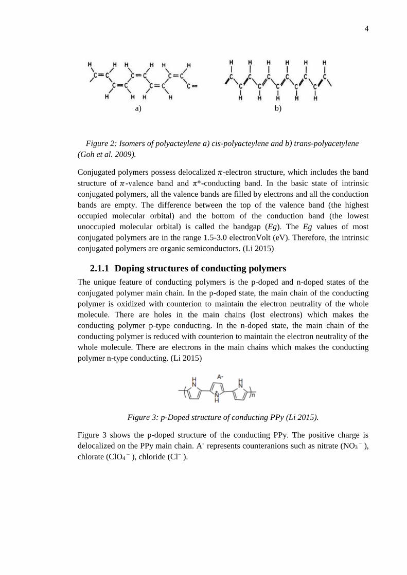
Figure 3: p-Doped structure of conducting PPy (Li 2015).
Figure 3 shows the p-doped structure of the conducting PPy. The positive charge is
delocalized on the PPy main chain. A- represents counteranions such as nitrate (NO3 − ),
chlorate (ClO4 − ), chloride (Cl− ).

5
Figure 4: Conductivities of insulators, semi-conductors, metals and conjugated
polymers (The Nobel Prize in Chemistry 2000).
The number of counteranions per monomer unit of the conducting polymer (or the
concentration of the charge carrier in the conjugated main chain of the conducting
polymer) is called the doping degree of the conducting polymer. The maximum doping
degree is related the main polymer chain structure. For example, the doping degree for
polyacetylene is usually 0.1-0.2, 0.25-.0.35 for polypyrrole, 0.4-0.5 for polyaniline, 0.3-
0.4 for polythiophene. For the p-doped polypyrrole, the doping degree of 0.25-0.35
implies that the conjugated chain including 3-4 pyrrole units can be doped with 1
counterion (or there is a hole within the polypyrrole main chain containing 3-4 pyrrole
units), as shown in Figure 3. The doping degree is much higher in conducting polymers
where the charge carrier concentration reaches 1021 /cm3. This value is several orders
higher than that of inorganic semiconductors as shown in Figure 4. In addition, the
doping in conducting polymers also results in morphology changes and volume
expansion because of the counteranion doping. (Li 2015)
2.1.2 Charge carriers in conducting polymers
For trans-polyacetylene with the degenerate basic state, the charge carriers are polarons
and solitons. For the basic state nondegenerate cis-polyacetylene, PPy, PTh, Pani. the
charge carriers are polarons and bipolarons. The soliton is an unpaired 𝜋 -electron
resembling the charge on free radicals. It can be delocalized on a conjugated polymer
chain. The neutral soliton can be oxidized to lose an electron and form a positive
soliton, or it can be reduced to gain an electron to become negative soliton. The soliton
possesses a spin of 1/2 whereas there is no spins for positve and negative solitons.
Polarons are the major charge carriers in conducting polymers including basic state
degenerate trans-polyacetylene and the basic state non degenerate conjugated polymers.
P+ denotes positive polaron which is formed after oxidation of the conjugated polymer
main while and P- denotes negative polaron which is formed after the reduction of the
conjugated polymer main chain. P+ and P- possess spin of 1/2. (Li 2015)

6
Figure 5: Polaron and bipolaron formation upon oxidation (p-doping) of polypyrrole
(Jangid et al 2014).
The bipolaron is the charge carrier that possesses double charges by coupling of two P+
or two P- on a conjugated polymer main chain. It has no spin and can be formed when
the concentration of polarons are high in the conjugated polymer main chains. The
positive bipolaron and negative bipolaron correspond to the hole pair or the electron
pair. Figure 5 shows the polaron and bipolaron structure of polypyrrole upon oxidation.
(Li 2015)
2.1.3 Doping characteristics
Doping of conducting polymers can be realized chemically or electrochemically by
oxidation or reduction of the conjugated polymers. (Li 2015)
2.1.3.1 Chemical doping
The chemical doping includes p-type doping and n-type doping. p-Doping is also called
oxidation doping, which refers to the oxidation process of the conjugated polymer main
chain to form polarons. The oxidants like Iodine (I2), Bromine (Br2), Arsenic
pentafluoride (AsF5), etc. can be used as p-dopants. After p-doping, the conjugated
polymer is oxidized and loses electron to form p-doped conjugated polymer chain, and

7
the dopant gains an electron to become the counteranion. The p-doping process can be
realized from the following reaction:
(1)
where CP denotes conducting polymers.
n-Doping is also called reduction doping, which refers to the reduction process of the
conjugated polymer main chain to form negative charge carriers. The reductants like
alkali metal vapor, sodium naphthalenide (Na+ (C10H8) − ), etc. can be used as n-
dopants. After n-doping, the conjugated polymer is reduced and gains electron to form
n-doped conjugated polymer chain, and the dopant losses an electron to become the
countercation. The n-doping process can be realized from the following reaction:
(2)
where CP is the conducting polymer.
2.1.3.2 Electrochemical doping
Electrochemical doping is realized by electrochemical oxidation of reduction of the
conjugated polymers on an electrode. For electrochemical p-doping, the conjugated
polymer main chain is oxidized to lose an electron (gain a hole) where the doping of
counteranions is accompanied from electrolyte solution :
(3)
where A- denotes the solution anion, CP+(A-) represents the main chain oxidized
conducting polymer and counteranion doped. (Li 2015)
For electrochemical n-doping, the conjugated polymer main chain is reduced to gain an
electron where the doping of countercations is accompanied from electrolyte solution:
(4)
where M+ denoted solution cation, CP-(M+) represents the main chain reduced
conducting polymer polymer and countercation doped. (Li 2015)
The electrochemical doping is simple and reproducible, and it can be carried out
amperometrically or potentiostatically or with a cyclic scan of a potential
(voltammetric). (George et al. 2006) It is usually performed in an electrochemical cell.

8
The electrochemicall cell can be of three types used to fabricate the conducting
polymers: (Yang & Martin2004).
a) current-controlled (galvanostatic) method: A current source is attached between
working and counter electrodes and a user-defined current is passed.
b) voltage-controlled (potentiostatic) method: A current is pushed between working
electrode and counter electrode as required to control the working electrode potential
with respect to a reference electrode.
c) VWE-CE control (voltammetric): A voltage source is applied between the working and
counter electrodes. The potential of these electrodes with respect to reference electrode
are not controlled. Here only the net potential between working and reference electrodes
are controlled.
The electrodeposition process is very fast, and takes usually a few seconds. The film
thickness can be easily calculated with the measurement of total charge in the formation
of CPs. In the same way, the final potential and the anion (or anions) of the supporting
electrolyte regulates the level of doping as well as the oxidation state and conductivity
of polymer. The final polymer can reach conductivities upto 1.0-105 S/cm. (George et
al. 2006)
2.1.4 Application of CPs
Conducting polymers (CPs) are discovered over 30 years ago with a growing interest on
their electronic conducting properties and unique biophysical properties. Some of the
applications of the CPs are:
a) Chemical sensors: Conducting polymers such as PPy, Pani, PTh, and their derivatives
have been used as the active layers of the gas sensors (McQuade et al. 2000).
b) Drug delivery: The biocompatibility of CPs opens up the possibility for them to be
used as in vivo biosensors applications for continuous monitoring of drugs or
metabolites in biological fluids (Harwood & Pouton 1996).
c) Bioactuators: Bioactuators are the device which are used to create mechanical force,
which in turn can be used to create artificial muscles. The process of change in the
volume of CP scaffold upon electrical stimulation has been amployed in the
development of bioactuators (Ravichandran et al. 2010).
d) Tissue engineering applications: The desired properties of CPs for tissue engineering
applications are conductivity, reversible oxidation, redox stability, biocompatibility,
hydrophobicity, three-dimensional geometry and surface topography. They are widely
used in tissue engineering applications because of their ability to subject cells to an
electrical stimulation (Ravichandran et al. 2010).

9
e) Biosensors: CPs acts as an excellent materials for the immobilization of biomolecules
and fast electron transfer for the development of efficient biosensors. They are used to
enhance speed, sensitivity and versatility of biosensors in diagnostic medicine to
measure vital analytes in the human body and thus are widely used in medical
diagnostic reagents (Heller 1990).
They have also attracted much interest as a suitable matrix for the entrapment of
enzymes. The ideas of incorporating of enzymes into electro-depositable conducting
polymeric films permit the localization of biologically active molecules on electrodes of
any size or geometry, mostly for the fabrication of multi-analyte micro-amperometric
biosensors. (Unwin & Bard 1992)
They are also known to be compatible with biological molecules in neutral aqueous
solutions. They can be reversibly doped and undoped electrochemically along with
significant changes in conductivity and spectroscopic properties of the film that can be
used as a signal for the biochemical reaction. The electronic conductivity of CPs
changes in response to change in pH and redox potential of their environment. (Paul et
al.1985)
They have the ability to transfer electric charge produced by biochemical reaction to
electronic circuit. It can be deposited over a desired area of electrodes. This property of
CPs together with the possibility to entrap enzymes during EP has been exploited for
the development of amperometric biosensors. (Foulds & Lowe 1986)
Other applications include corrosion protection layer, solar cells, Field-Effect Transistor
(FET) sensors and chemiresistors (Gerard et al. 2002).
2.1.5 Polypyrrole
Polypyrrole (PPy) is an electrically conducting polymer that can be polymerized
electrochemically and deposited onto the electrodes. PPy is one of the most widely
studied electroactive conducting polymer because of its solubility in aqueous solution
and low oxidation potential of the monomer, ease of use, controllable surface properties
and compatibility with the mammalian cells. (Harris et al. 2013) It can be doped with
various counterions ions to change its physical, chemical and electrical properties
(George et al. 2005). The ability to control PPy surface properties such as charge
density and wettability initiate the potential for modifying neural interactions with the
polymer (Cui et al.2001). It enables flexibility in the design of three-dimensional
polymer implants because of ease of fabrication and the ability to control its growth rate
(Lavan et al. 2003). PPy is a relatively soft material when coated on the surface of the
electrodes which promotes cell attachment onto the surface (Heim et al. 2012).
10
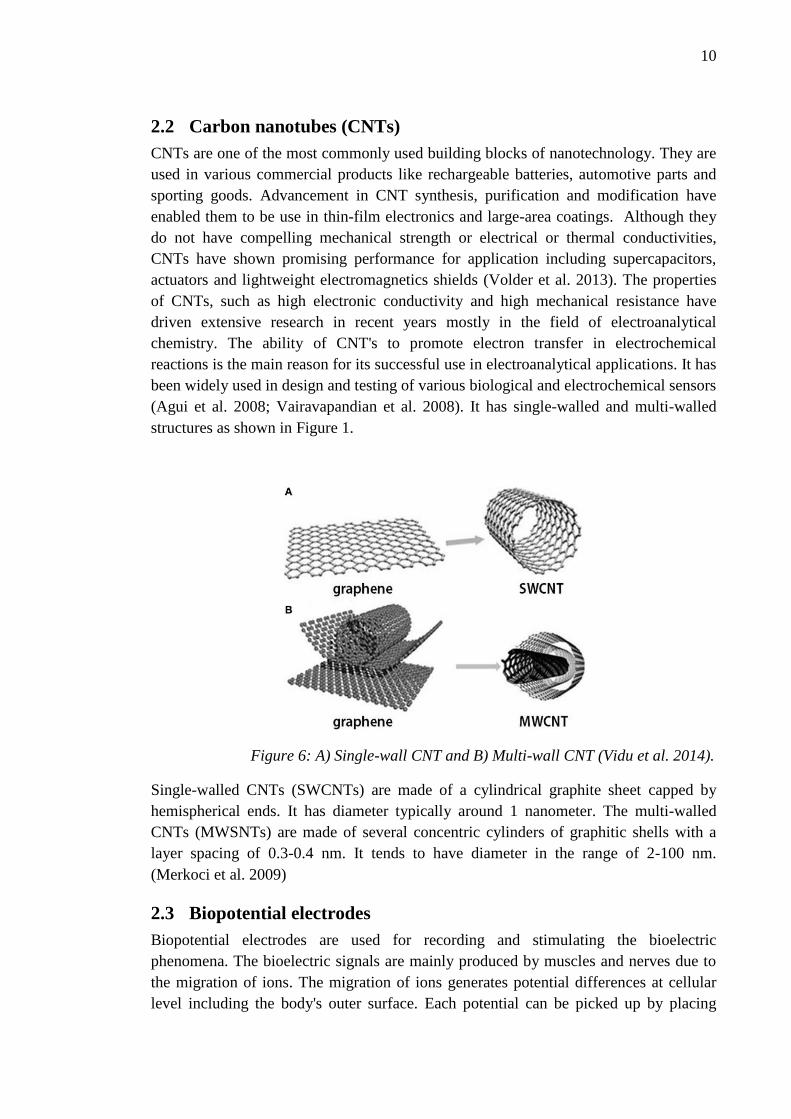
2.2 Carbon nanotubes (CNTs)
CNTs are one of the most commonly used building blocks of nanotechnology. They are
used in various commercial products like rechargeable batteries, automotive parts and
sporting goods. Advancement in CNT synthesis, purification and modification have
enabled them to be use in thin-film electronics and large-area coatings. Although they
do not have compelling mechanical strength or electrical or thermal conductivities,
CNTs have shown promising performance for application including supercapacitors,
actuators and lightweight electromagnetics shields (Volder et al. 2013). The properties
of CNTs, such as high electronic conductivity and high mechanical resistance have
driven extensive research in recent years mostly in the field of electroanalytical
chemistry. The ability of CNT's to promote electron transfer in electrochemical
reactions is the main reason for its successful use in electroanalytical applications. It has
been widely used in design and testing of various biological and electrochemical sensors
(Agui et al. 2008; Vairavapandian et al. 2008). It has single-walled and multi-walled
structures as shown in Figure 1.
Figure 6: A) Single-wall CNT and B) Multi-wall CNT (Vidu et al. 2014).
Single-walled CNTs (SWCNTs) are made of a cylindrical graphite sheet capped by
hemispherical ends. It has diameter typically around 1 nanometer. The multi-walled
CNTs (MWSNTs) are made of several concentric cylinders of graphitic shells with a
layer spacing of 0.3-0.4 nm. It tends to have diameter in the range of 2-100 nm.
(Merkoci et al. 2009)
2.3 Biopotential electrodes
Biopotential electrodes are used for recording and stimulating the bioelectric
phenomena. The bioelectric signals are mainly produced by muscles and nerves due to
the migration of ions. The migration of ions generates potential differences at cellular
level including the body's outer surface. Each potential can be picked up by placing

11
electrodes at any two points at the surface of the body and measured with a recording
device. A typical cell potential waveform is shown in Figure 2. (Indian Institute of
Technology 2010)
Figure 7: A typical cell potential waveform (Indian Institute of Technology 2010).
When a cell is excited by ionic currents or external stimulus, the membrane potential of
a cell changes from its original state. The potential rises due to high influx of sodium
ions and reaches the maximum value, which is called action potential. An exciting cell
with an action potential is said to be depolarized; this process is called depolarization.
After a certain time, the cell becomes polarized and returns back to it's resting potential.
This process is known as polarization. After an action potential, there is a period, known
as absolute refractory period, in which cell does not respond to any new stimulus. This
is followed by a relative refractory period when another action potential may be
triggered by a stronger stimulus.
One of the important desirable characteristics of electrodes to pick up these signals is
that they should not polarize, meaning that the electrode potential must not vary
considerably even when the current is passed through the electrode. Other properties of
good electrode includes biocompatibility, good electrical conductivity and corrosion
resistance. (Indian Institute of Technology 2010)
2.3.1 Electrode-electrolyte interface
A redox reaction needs to occur at the interface between the electrode and electrolyte
for a charge to be transferred between electrode and the ionic solution. A redox reaction
is an electrochemical oxidation-reduction reaction. The oxidation is dominant when the
current flow is from the electrode to the electrolyte, and the reduction dominate when
the current flow is in the opposite. There are two kinds of currents: faradic current due

12
to the charge transfer through the interface and displacement current arising from the
displacement of charge carriers at the interface. The displacement current is also called
as capacitive current. (Riistama 2010; Woo 2015) An electrode-electrolyte interface is
shown in Figure 3.
Figure 8: Electrode-electrolyte interface (Woo 2015).
When the metallic atoms of the electrode are oxidized, the reaction can be stated as:
C ↔ Cn+ +n(e-) (5)
where C represents the metal atom, n its valence, e- an electron and n(e-) number of
electrodes. When the reduction/oxidation of the electrolyte ions is to occur, the reaction
will be written as:
An- ↔ A+ n(e-)
(6)
where An- represents an anion atom or molecule of the electrolyte solution and A is the
atom or molecule of the electrolyte.

13
Thus, the net current crossing the electrode-electrolyte interface are: a) electrons
moving in an opposite direction of current, b) cations (C+) moving in the same direction
as current and c) anions (A-) moving in an opposite direction of current. These redox
reaction causes a changes in the charge distribution between the interface and rest of the
electrolyte. The charge distribution at the interface can be measured as the higher
electrode potential than in the bulk electrolyte. The layer with a high charge density at
the interface is called a double layer. (Riistama 2010; Woo 2015)
2.3.2 Electrical characteristics
The electrical characteristics of a biopotential electrode can be represented by RC
circuit in Figure 4 below. In the circuit below, Cd is the capacitance across the charge
double layer, Rd is the leakage resistance across the charge double layer, Rs is the
resistance of electrolyte and Ehc is the Dc voltage source or half call potential. Rd and Cd
are the impedance associated with the electrode-electrolyte interface and polarization
effects. Rs is the series resistance associated with the interface effects and due to
resistance in the electrolyte. The value of Cd and Rd changes with frequency, current
density, electrode material and electrolyte concentration whereas value of Rs changes
with electrolyte concentration. (Woo 2015)
Figure 9: The equivalent circuit for a biopotential electrode in contact with an
electrolyte (Woo 2015).
The impedance of the electrode is frequency dependent as show in Figure 5. At low
frequencies the impedance is dominated by the series combination of Rs and Rd,
whereas, at higher frequencies Cd bypasses the effect of Rd so that impedance is now
close to Rs. Thus, it is possible to determine the component values for the equivalent
circuit for a electrode by measuring the impedance at high and low frequencies.

14
Figure 10: An example of biopotential electrode as a function of frequency (Neuman
2000).
The impedance is characterized by a magnitude (|Z|) and phase angle (ϴ) and is most
generally represented as a function of frequency. For a capacitor, the impedance is
purely imaginary, the phase angle is 90° and the current is out of phase with voltage by
90°. For a resistor, the impedance is real, the current and voltage are in phase and the
phase angle is 0°. For a system composed of combination of these components like in
the electrical electrode-electrolyte interface, a large phase angle value indicates that the
impedance is predominantly capacitive, while small angle values are resistive. (Cui et
al. 2001) The electrical characteristics of electrodes are also affected by it's physical
properties which is shown in Table 1below. It is seen that the increase in surface area
and surface roughness of the electrode decreases the electrode impedance. However,
polarization of the electrodes increases the electrode impedance at lower frequencies.
Table 1:The Effect of Electrode Properties on Electrode Impedance (Neuman 2000).
Property Change in Property Changes in Electrode Impedance
Surface area
Polarization At low frequencies
Surface roughness
2.3.3 General requirements of the electrode material
The noble metals electrode like platinum(Pt), gold, iridium, palladium and rhodium
have been commonly used for electrical stimulation. Their intended application might
be different due to their material properties. Platiunum is relatively soft material and
may not be mechanically acceptable for all stimulation applications. Iridium is harder
than Platinum making it more suitable as intracortical electrodes. (Merrill et al. 2005)
Some of the basic requirement criteria of an electrode material are listed in Table 2
below.

15
Table 2: Basic requirements of an electrode material (Merrill et al. 2005).
Biocompatibility The electrode material should be biocompatible
to avoid a necrotic cell response.
Stable junction A stable junction should be formed between
electrode and tissue, especially in long term in
vitro and in vivo measurements.
Mechanical strength Electrode material should offer sufficient
mechanical strength combined with stable
electrical properties for reliable long term
performance of MEA.
High charge injection
capacity
A safe stimulation conditions for reliable
stimulation of excitable tissue can be achieved
by a sufficient high charge capacity per surface
area.
Electrical conductivity A good electrical conduction between electrode
and tissue is crucial for stimulation and
recording of bioelectrical signals.
Corrosion resistance An electrode material should not erode in
biological environment when implanted.
2.3.4 Safe charge injection limit and stimulation protocol
The two most important parameters for designing a stimulation protocol is: a)
Efficiency and b) safety. An efficient stimulation pulse requires to have a sufficient high
charge per pulse whereas a safety pulse requires a sufficient low charge per pulse to
prevent electrode corrosion. (Merrill et al.2005) The maximum safe charge that can be
injected through a microelectrode depends on several factors including the electrode
material, the electrolyte, stimulation parameters (charge per pulse, duration, waveform
type, frequency) as well as the shape and size of the electrode. Microelectrodes of small
dimensions may safely inject less charge than macroelectrodes, however the efficiency
may be compromised in such case. Therefore, sufficient charge injection into the
microelectrode often brings the limiting factor for the efficient stimulation of the
surrounding tissues with electrodes. One way to overcome this problem is by increasing
the effective surface area of the microelectrodes, which decreases the impedance and
the thermal noise of the electrode and also allows to inject higher charges, necessary for
efficient and reliable stimulation of excitable tissues. (Heim et al. 2012)
The basic design criteria for a safe stimulation protocol can be stated according to
Merrill et al.2005 as: "The electrode potential must kept within a potential window
where irreversible faradic reactions do not occur at levels that are intolerable to the

16
physiological system or electrode. If irreversible faradic reactions do occur, one must
ensure that they can be tolerated (e.g. that physiological buffering systems can
accomodate any toxic products) or that their detrimental effects are low in magnitude
(e.g. that corrosion occurs at a very slow rate and the electrode will last for longer than
its design lifetime)." Therefore, currents injected into a microelectrode should not
exceed a certain safe limit to avoid irreversible faradic reactions at the electrode surface.
2.3.5 Charge vs charge density relationship
According to Shannon (1992),an expression for the maximum safe level for stimulation
is given by :
log(Q/A) = k-log(Q) (7)
where Q is the charge (µC) per phase, Q/A is charge density (µC/cm2) per phase and
2.0 >k > 1.5, where k is constant which fits to the empirical data findings in the above
research(Merrill et al. 2005). Figure 6 illustrates the charge vs charge density
relationship of equation (4) using k values of 1.7, 1.85, and 2.0.
Figure 11: Charge (Q) vs. charge density (Q/A) for safe stimulation at the frequency of
50 Hz. A microelectrode with relatively small total charge per pulse might safely
stimulate using a large charge density, whereas a large surface area electrode (with
greater total charge per pulse) must use a lower charge density. (Merrill et al. 2005)
The data shows that as the charge per phase increases, the charge density for safe
stimulation decreases. Above the threshold for damage, experimental data demonstrates
tissue damage, and below the threshold line, the data indicates no damage. When the
total charge is small as with a microelectrode, a relatively large charge density may
safely be used. It is seen that both charge per phase and charge density are important
parameters that determines the neuronal damage to cat cerebral cortex. In terms of the
mass action theory of damage, charge per phase determines the total volume within
which the neurons are excited, and the charge density determines the proportions of

17
neurons that are close to an excited electrode. (Merrill et al. 2005) The area of safe
stimulation also depends upon the types of tissues stimulated (mass action theory)
(McCreery et al.1990). For example, the limits for safe stimulation in deep brain was
found to be 30 µC/cm2 for an injected charge of 2 µC per phase (Kuncel & Grill 2004).

18
3 MATERIALS AND METHODS
3.1 Material and solution preparation
We used Pyrrole (Py) monomer (Sigma Aldrich, St. Louis, USA)of concentration0.2 M
and Dodecyl-benzene sulphonate (DBS) (Acros Organics, Geel, Belgium) concentration
of 0.05 M to make the solutions. A (PPy)-DBS solution was made by adding 1.39 ml of
Py solution and 1.98 g of DBS to 100 ml of distilled water. We used magnetic stirrer for
30 minutes to achieve homogenous solution. We had single-walled carbon nanotubes
(SWCNTs) functionalized with COOH (University of Oulu) of three different
concentrations. We used three different concentrations of CNTs: 0.1 mg/ml, 0.25 mg/ml
and 0.5 mg/ml of COOH/DI-water. The chemical structures of these chemicals are
shown in Figure 7 below.
Figure 12: The chemical structures of a) DBS b) Py monomer (Royal Society of
Chemistry2015). c) PPy (Chidichimo et al. 2010). d) CNT (C29H42O10, MW 550.64)
(Yang et al. 2014).
We used two types of platinum electrodes for the coatings, MEA electrodes and
macroelectrodes. MEA electrodes (MEA60 100 Pt, Qwane Biosciences, City, Country)
consisted of 60 recording electrodes with a diameter of 30 µm and interelectrode
distance of 100 µm. The size of the MEA electrode array is 15mm*15mm*0.7mm.

19
Each electrode has impedance value of 800-1100KOhm at frequency of 1KHz.
Macroelectrode were made of 99.95% Pt with the dimensions of 1.0mm*0.5mm*15
mm (Labor-Platina Kft, Pilisvörösvár, Hungary). We used PPy-DBS and PPy-
DBS/CNT solutions for macroelectrode coating while only PPy-DBS solution for MEA
electrode coating. The coating solution used for each type of coating is presented in
Table 3 below.
Table 3: Electrodes and coating solutions used.
Electrode types Coating solution
MEA electrodes PPy-DBS
Macroelectrodes PPy-DBS
PPy-DBS+CNT
0.1mg/ml
PPy-DBS+CNT
0.25mg/ml
PPy-DBS+CNT
0.5mg/ml
3.2 Polymerization
The electrochemical polymerization was carried out using a potentiostatic step method
at a constant voltage in a two-electrode electrochemical cell as shown in Figure 8
below. The coating solution for each electrode types are listed in Table 3. All the
electrodes were polymerized by using VersaSTAT Series potentiostat/galvanostat
device controlled by VersaStudio software (Princeton Applied Research, South Illinois,
USA). We used the linear scan voltammetry and chronopotentiometry technique to
generate the current and charge density curves.
We controlled the process by charge limits. The settings for the each electrodeposition
are listed in the Results section 3.1 later. The experiment were carried out at room
temperature. The data from the software was exported to CView software (Scribner
Associates, North Carolina, USA) to further analyze the data.
The electrode to be coated (working electrode) was supplied with certain potential (V)
with respect to the reference electrode from the potentiostat and the current (I) was
measured from the counter electrode. We used Pt counter electrode of dimesnions
1.0mm*0.5mm*15 mm (Labor-Platina Kft, Pilisvörösvár, Hungary). We used 12ml of

20
solution for macroelelectrode coating and 2ml for microelectrodes coating. The values
of currents, voltages and times are given in Result section later.
Figure 13: Electrochemical cell setup (Li & J 2010).
3.3 Impedance measurement
We used two devices for the impedance measurement. The MEA electrodes impedance
was measured with Impedance testing device MEA-IT (Multi Channel Systems,
Reutlingen, Germany). The macroelectrodes were measured with Solartron Model
1260A Frequency Response Analyzer in combination with 1294A Impedance Interface
and SMaRT Impedance Measurement Software (Solartron Analytical, Hampshire, UK).

21
Figure 14: a) Mounting the MEA electrodes b) MEA-IT device and c) Ag-Agcl silver
wire ground electrode d) Virtual MEA layout e) Measurement with MEA-IT software
and f) Measured electrode impedance (Impedance Testing Device MEA-IT
Manual2013).
First we carefully inserted the MEA in the middle of the lid as shown in Fig 9 a) making
sure that it is correctly oriented. Then, we filled the MEA dish with a conducting
Phosphate Buffered saline (PBS) solution (Sigma Aldrich, St. Louis, USA) and
approximately fifteen minutes was waited before measuring the electrodes. At the same
time, we externally grounded Ag-Agcl silver wire even though we measure a MEA with
internal reference electrode as seen in Fig 9 c). Otherwise the impedance values would
be out of range. We used MEA-IT software (Multi Channel Systems, Reutlingen
,Germany) to control the impedance measurement as seen in Figure 9.
3.3.1 Macroelectrode impedance measurement
We used Solartron Model 1260A Frequency Response Analyzer, 1294A Impedance
Interface and computer equipped with the SMaRT Impedance Measurement Software
(Solartron Analytical, Hampshire, UK) to measure the impedance.

22
We used three-electrochemical cell setup for impedance measurement as shown in
Figure 10 below. We used MF-2052 RE-5B Ag/AgCl reference electrode with flexible
connector (Labor-Platina Kft, Pilisvörösvár, Hungary), Pt as a counter electrode and Pt
sample as a working electrode. The potential (V) was supplied between reference and
working electrode and the current flow between WE and CE was measured. We used
10ml PBS solutions as electrochemical solution. The dc level voltage and ac voltage
were set to 0V to 5mV, respectively. Impedance was measured at 26 discrete frequency
points from 1.0 Hz to 100 000 Hz using frequency sweep option. These measurements
were analyzed by using Smart v3.2.1 software (Solartron Analytical, Hampshire, UK)
and Microsoft Excel (Microsoft, Washington, USA).
Figure 15: Three-electrode electrochemical setup (Ayoub et al. 2016).
3.4 Imaging device
We used Wyko NT1100 Optical Profilometer, (Veeco, City, Country), Park XE-
100AFM Atomic Force Microscopy (Park Systems, Santa Clara, USA), and Olympus
BH-2Optical microscope (Olympus Optical Co., Tokyo, Japan) equipped with a
BestScope BUC4-500C5.0 MP digital camera (BestScope International Limited,
Beijing, China) to capture the images of the coated electrodes.
3.4.1 Optical Profilometer
We used Wyko NT1100 Optical Profilometer to capture the 3D image of
macroelectrodes. The basic principle and the measurement of the device is described
below in Fig 11 and Fig 12 respectively.

23
3.4.1.1 Principle
Optical Profilometer uses the wave properties of light to compare the optical path
difference between a test surface and a reference surface. A light beam is split,
reflecting half the beam from a test material which is passed through the focal plane of
microscope objective, and the other half of the split beam is reflected from the reference
mirror. Interference occur in the combined beam wherever the length of the light beams
vary. The interference beam is focused into a digital camera to create light and dark
interference image as shown in Figure 11 below. With a known wavelength, the height
differences across a surface is calculated. From these height differences, a surface 3D
map is obtained. (Zygo Corportion 2017)
Figure 16: Schematic of an optical profilometer (Zygo Corportion 2017).
3.4.1.2 Measurement
First of all, the profilometer was calibrated in Vertical Scanning Interferometry (VSI)
measurement mode with VSI calibration sample as shown in Figure 12 below. The
sample was mounted on the Profilometer stage and the program was started by double
clicking the Vision64 software icon, to open the calibration mode. We selected the filter
to VSI mode and adjusted the intensity and focus with the slider in the computer
window. The illumination was increased until we see red on the screen and decreased
the illumination until the red was un-illuminated. Then the calibration sample was
focused by rotating the focus Knob slowly until we get the good contrast image of the
sample. Then, we repeated the process with the Pt samples and the images were saved
in a suitable format.

24
Figure 17: Measurement with Optical Profilometer Vision software with intensity
window a), Calibration window b), Veeco NT1100 c) and Measurement option window
d) (Marcel 2003).
3.4.2 Atomic Force Microscopy (AFM)
We used Park XE-100AFM Atomic Force Microscope, to image the surface
topography of coated electrode. We calculated the peak-to-valley roughness index(Ra)
of the image using the vertical height of the image surface (The Research membranes
Environment, 2009) in Figure 26 below in the Results section. The basic measurement
and hardware setup are shown below in Figure 13 and Figure 14, respectively.

25
Figure 18: Basic AFM principle (Stonecypher 2011).
3.4.2.1 Principle
An AFM uses a cantilever tip to scan over a sample surface. As the tip approaches the
surface, attractive forces between the tip and surface causes the cantilever to deflect
towards the surface. However, if the tip makes contact with the surface, repulsive force
takes over and causes the cantilever to deflect away from the surface. A laser beam is
used to detect deflections away or towards from the surface. A deflection in the
cantilever causes the changes in the direction of the reflected beam. The photodiode can
be used to measure these changes and thus the topography of the sample image can be
created with feedback and electronic circuits. (Stonecypher 2011)

26
Figure 19: Basic hardware setup of Park XE-100 AFM (Fei & Brock 2013).
3.4.2.2 Measurement
First we mounted sample on the stage and rested the tips in the tips box and that
bearings fits into tip slots. Then we replaced head and pushed flaps away until slightly
tight. Then after, we checked the Scanning probe mcroscopy (SPM) Controller and
Monitors. We turned on the Light Bank, isolation stage and Laser light. After that, we
processed the image with 'XEC' program and saved it. (Fei & Brock 2013)
3.4.3 Optical Microscope
Olympus BH-2Optical microscope (equipped with a BestScope BUC4-500C, 5.0
MPdigital camera) was used to capture the mircographs image. The micrographs were
taken at 5X, 10x and 20x magnifications.

27
4 RESULTS
4.1 MACROELECTRODES
The macroelectrodes were successfully electrodeposited with PPy and PPy/CNT
solutions. The electrodeposited electrodes are: PPy-Control, PPy-CNT 0.1, PPy-CNT
0.25 and PPy-CNT 0.5. Their impedances were measured using Electrical Impedance
Spectroscopy and the images were analysed with AFM, Optical Profilometer and
Optical Microscope. The electrodeposition results are presented in section 4.1.1. The
Electrical Impedance Spectroscopy and impedance measurement results are presented in
section 4.1.2 to 4.1.4. The imaging results are presented in section 4.1.5.
4.1.1 Macroelectrode electrodeposition
All electrodes were polymerized using chronopotentiometry method with a reference
potential of 1.0 V. We used charge limit of 0.258C/cm2 and electrode area of 0.15cm2
for electrodeposition. The electrodes were successfully polymerized with PPy and
combination of PPy and CNT solutions. All the electrodes showed almost similar
charge and current density values. The results looked more consistent in each coating
than with the microelectrodes plates. PPy-CNT 0.25 showed the maximum current
density of 0.0023A/cm2 as seen in Figure 15 below. All the current density curves
reached the peak and then decreased within a second after the deposition process. After
a period of some seconds, all the current density curves decreased at constant value of
0.002A/cm2.

28
a) b)
Figure 20: Charge a) and current b) densities during electrodeposition.
All the coated platinum samples showed linear increase in charge density as in fig a).
Also PPy-Control and PPy-CNT 0.5 showed almost similar response and had a higher
time duration of about 1500sec than PPy-CNT 0.1 and PPy-CNT 0.25 samples. No
major difference was seen in the current curve as in fig b). PPy-CNT 0.25 showed
maximum current density within a few seconds of the electrodeposition process.
4.1.2 Electrical Impedance Spectroscopy
Figure 16 below shows the average bode plot measurements of various samples. PPy-
CNT 0.25 showed the highest impedance magnitude while PPy-CNT 0.5 showed lowest
value upto frequency of 100Hz. However, the values were very closer after frequency of
100Hz. Bare Pt samples had the highest negative phase angle value upto a frequency of
900 Hz. After this frequency, PPy-CNT 0.25 showed highest negative values. PPy-CNT
0.5 showed least negative phase angle after a frequency of 300Hz. It is seen that the
average Bare Pt samples had a dominant capacitive impedance until a frequency of
0 500 1000 1500 20000
0,1
0,2
0,3
Time (Sec)
Q (
Co
ulo
mb
s/c
m2)
PPy Control.parPPy CNT 0.1.parPPy CNT 0.25.parPPy CNT 0.5.par
0 500 1000 1500 20000
0,001
0,002
0,003
Time (Sec)
I (A
mp
s/c
m2)
PPy Control.parPPy CNT 0.1.parPPy CNT 0.25.parPPy CNT 0.5.par

29
around 300Hz after which PPy-CNT 0.25 was more capacitive. The electrode
impedance was reduced with PPy/CNT composition at lower frequencies, however,PPy-
CNT 0.25 was an exception.
a)
b)
Figure 21: a) Average Bode plot of different Pt samples Impedance plot a) and phase
plot b).
0
5000
10000
15000
20000
25000
30000
35000
1 10 100 1000 10000 100000
|Z|
Frequency (Hz)
Impedance Average Pt samples
Bare Pt
PPy Control
PPy-CNT 0.1
PPy-CNT 0.25
PPy-CNT 0.5
-90
-80
-70
-60
-50
-40
-30
-20
-10
0
10
1 10 100 1000 10000 100000
the
ta
Frequency (Hz)
Phase Average Pt samples
Bare Pt
PPy Control
PPy-CNT 0.1
PPy-CNT 0.25
PPy-CNT 0.5
30
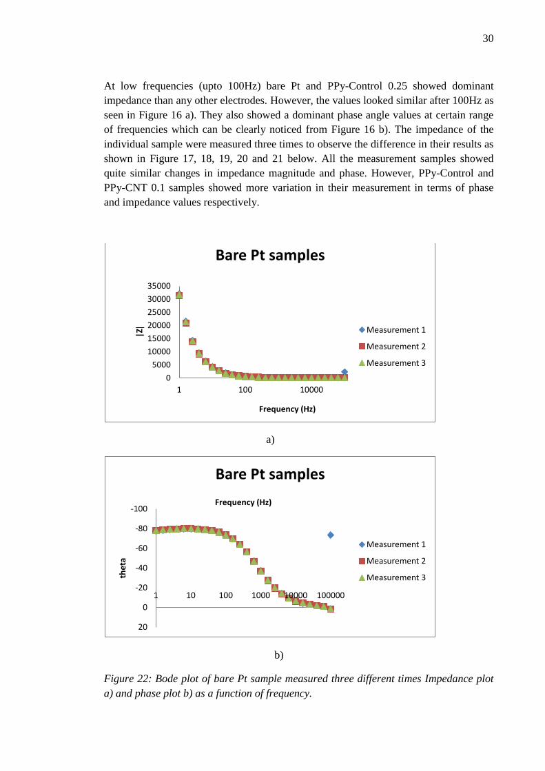
At low frequencies (upto 100Hz) bare Pt and PPy-Control 0.25 showed dominant
impedance than any other electrodes. However, the values looked similar after 100Hz as
seen in Figure 16 a). They also showed a dominant phase angle values at certain range
of frequencies which can be clearly noticed from Figure 16 b). The impedance of the
individual sample were measured three times to observe the difference in their results as
shown in Figure 17, 18, 19, 20 and 21 below. All the measurement samples showed
quite similar changes in impedance magnitude and phase. However, PPy-Control and
PPy-CNT 0.1 samples showed more variation in their measurement in terms of phase
and impedance values respectively.
a)
b)
Figure 22: Bode plot of bare Pt sample measured three different times Impedance plot
a) and phase plot b) as a function of frequency.
0
5000
10000
15000
20000
25000
30000
35000
1 100 10000
|Z|
Frequency (Hz)
Bare Pt samples
Measurement 1
Measurement 2
Measurement 3
-100
-80
-60
-40
-20
0
20
1 10 100 1000 10000 100000
the
ta
Frequency (Hz)
Bare Pt samples
Measurement 1
Measurement 2
Measurement 3

31
No major difference in the measurement was seen either from impedance magnitude or
phase plot. The maximum impedance magnitude of bare Pt sample was around
32000Ohm at the frequency of 1.0Hz. A sharp decrease in impedance magnitude was
then observed until the frequency of the 90Hz. The value at this frequency was around
350 Ohm. The values looked consistent after this frequency. The maximum phase angle
was around -80°. The phase angle showed almost all similar values until the frequency
of 90Hz. After this frequency, the phase angle sharply decreased until the frequency
about around 9000Hz. After this frequency, the variation in phase angle values was
slower.
a)
b)
Figure 23: Bode plot of PPy-Control sample measured three different times Impedance
plot a) and phase plot b) as a function of frequency.
0
2000
4000
6000
8000
10000
12000
14000
16000
18000
1 100 10000
|Z|
Frequency (Hz)
PPy control samples
Measurement 1
Measurement 2
Measurement 3
-70
-60
-50
-40
-30
-20
-10
0
10
1 10 100 1000 10000 100000
the
ta
Frequecy (Hz)
PPy control samples
Measurement 1
Measurement 2
Measurement 3

32
The maximum impedance magnitude of PPy-Control sample was around 16400Ohm at
the frequency of 1.0Hz. A sharp decrease in impedance magnitude was then observed
until the frequency of the 90Hz. The value at this frequency was around 560 Ohm. The
values looked consistent after this frequency. The maximum phase angle was around -
60°. The phase angle showed almost all similar values until the frequency of 90Hz.
After this frequency, the phase angle sharply decreased until the frequency about around
9000Hz. After this frequency, the variation in phase angle values was slower.
a)
b)
Figure 24: Bode plot of PPy-CNT 0.1 sample measured three different times Impedance
plot a) and phase plot b) as a function of frequency.
0
5000
10000
15000
20000
25000
30000
35000
1 10 100 1000 10000 100000
|Z|
Frequency (Hz)
PPy CNT 0.1 samples
Measurement 1
Measurement 2
Measurement 3
-80
-70
-60
-50
-40
-30
-20
-10
0
10
1 10 100 1000 10000 100000
the
ta
Frequency (Hz)
PPy CNT 0.1 samples
Measurement 1
Measurement 2
Measurement 3

33
.No major difference in phase angle measurement was seen from fig b). However,
variation of impedance magnitude during the measurement was seen at lower
frequencies as in fig a).
The maximum impedance magnitude of PPy-CNT 0.1 electrode was around 16000Ohm
at the frequency of 1.0Hz. A sharp decrease in impedance magnitude was then observed
until the frequency of the 90Hz. The value at this frequency was around 520Ohm. The
values looked consistent after this frequency. The maximum phase angle was around -
70°. The phase angle showed almost all similar values until the frequency of 90Hz.
After this frequency, the phase angle sharply decreased until the frequency about around
9000Hz. After this frequency, the variation in phase angle values was slower.
a)
b)
Figure 25: Bode plot of PPy-CNT 0.25 sample measured three different times
Impedance plot a) and phase plot b) as a function of frequency.
05000
10000150002000025000300003500040000
1 100 10000
|Z|
Frequency (Hz)
PPY CNT 0.25 samples
Measurement 1
Measurement 2
Measurement 3
-70
-60
-50
-40
-30
-20
-10
0
1 10 100 1000 10000 100000
the
ta
Frequency (Hz)
PPy CNT 0.25 samples
Measurement 1
Measurement 2
Measurement 3

34
The maximum impedance magnitude of PPy-CNT 0.25 electrode was around
34400Ohm at the frequency of 1.0Hz. A sharp decrease in impedance magnitude was
then observed until the frequency of the 90Hz. The value at this frequency was around
550 Ohm. The values looked consistent after this frequency. The maximum phase angle
was around -60°. The phase angle showed almost all similar values until the frequency
of 90Hz. After this frequency, the phase angle sharply decreased until the frequency
about around 9000Hz. After this frequency, the variation in phase angle values was
slower.
a)
b)
Figure 26: Bode plot of PPy-CNT 0.5 sample measured three different times Impedance
plot a) and phase plot b) as a function of frequency.
0
2000
4000
6000
8000
10000
12000
14000
1 10 100 1000 10000 100000
|Z|
Frequency (Hz)
PPy CNT 0.5 samples
Measurement 1
Measurement 2
Measurement 3
-80
-70
-60
-50
-40
-30
-20
-10
0
10
1 10 100 1000 10000 100000
the
ta
Frequency (Hz)
PPy CNT 0.5 samples
Measurement 1
Measurement 2
Measurement 3

35
No variation in the impedance magnitude and phase angle was seen in Fig a) and b).
The maximum impedance magnitude of PPy-CNT 0.5 electrode was around 12000Ohm
at the frequency of 1Hz. A sharp decrease in impedance magnitude was then observed
until the frequency of the 90Hz. The value at this frequency was around 200 Ohm. The
values looked consistent after this frequency. The maximum phase angle was around -
70°. The phase angle showed almost all similar values until the frequency of 90Hz.
After this frequency, the phase angle sharply decreased until the frequency about around
9000Hz. After this frequency, the variation in phase angle values was slower.
4.1.3 Impedance measurement at frequencies of 1Hz and 1kHz
The impedance measurement of different electrodes were done three times. M1 means
the first measurement and so on. The measurement values of the samples: Bare Pt, PPy-
Control, PPy-CNT 0.1, PPy-CNT 0.25 and PPy-CNT 0.5 is shown in Table 4 below.

36
Table 4: Impedance magnitude and phase of different electrodes at 1.0Hz and 1000Hz.
Frequency(Hz) Impedance magnitude(Ohm) Phase (ϴ°)
Bare Pt M1 M2 M3 M1 M2 M3
1.0 32000 31250 31760 -80 -80 -80
1000 110 100 100 -40 -40 -40
PPy-Control M1 M2 M3 M1 M2 M3
1.0 10900 15600 16400 -60 -60 -60
1000 160 170 150 -40 -40 -40
PPy-CNT 0.1 M1 M2 M3 M1 M2 M3
1.0 11600 12800 16000 -70 -70 -70
1000 100 120 130 -30 -30 -30
PPy-CNT 0.25 M1 M2 M3 M1 M2 M3
1.0 34400 30380 29600 -60 -60 -60
1000 270 250 240 -60 -50 -50
PPy-CNT 0.5 M1 M2 M3 M1 M2 M3
1.0 12000 11700 11340 -70 -70 -70
1000 120 110 100 -40 -40 -40
The maximum impedance magnitude for bare Pt electrode was around 32000Ohm at the
first measurement at frequency of 1.0Hz, the while all the phase angle was equal to
around -80°. Similarly, the maximum magnitude at 1000Hz was around 110Ohm and
all the phase angle was equal to around -40°. The least magnitude at 1.0Hz and 1000Hz
was around 31250Ohm and 100Ohm respectively.
The maximum impedance magnitude for PPy-Control electrode was around 16400Ohm
at the third measurement at frequency of 1.0Hz, the while all the phase angle was equal
to around -60°. Similarly, the maximum magnitude at 1000Hz was around 170Ohm and
all the phase angle was equal to around -40°. The least magnitude at 1.0Hz and 1000Hz
was around 10900Ohm and 150Ohm respectively.
The maximum impedance magnitude for PPy-CNT 0.1 electrode was around
16000Ohm at the third measurement at frequency of 1.0Hz, the while all the phase

37
angle was equal to around -60°. Similarly, the maximum magnitude at 1000Hz was
around 130Ohm and all the phase angle was equal to around -40°. The least magnitude
at 1.0Hz and 1000Hz was around 11600Ohm and 100Ohm respectively.
The maximum impedance magnitude for PPy-CNT 0.25 electrode was around
34000Ohm at the first measurement at frequency of 1.0Hz, the while all the phase angle
was equal to around -60°. Similarly, the maximum magnitude at 1000Hz was around
270Ohm and all the phase angle was equal to around -50°. The least magnitude at
1.0Hz and 1000Hz was around 29600Ohm and 240Ohm respectively.
The maximum impedance magnitude for PPy-CNT 0.5 electrode was around
12000Ohm at the first measurement at frequency of 1.0Hz, the while all the phase angle
was equal to around -70°. Similarly, the maximum magnitude at 1000Hz was around
120Ohm and all the phase angle was equal to around -40°. The least magnitude at
1.0Hz and 1000Hz was around 11340Ohm and 100Ohm respectively.
4.1.4 Average measurement at 1.0Hz and 1.0kHz
The PPy-CNT 0.25 showed highest negative phase angle of 60° at frequency of 1.0kHz
while PPy-CNT 0.1 showed least negative value of -30°. PPy-CNT 0.25 also showed
least negative phase angle of -58° at 1.0Hz while bare Pt showed highest negative value
of -80°. This shows that PPy-CNT 0.1 was highly resistive at 1.0kHz while bare Pt was
highly capacitive at 1.0Hz.
Bare Pt showed high impedance values at 1Hz and least magnitude at 1.0kHz compared
to coated electrodes. PPy-CNT 0.25 showed maximum magnitude at 1.0Hz and PPy-
CNT 0.5 showed least magnitude at 1.0kHz. The average impedance and phase were
taken from the different measurement of the samples as shown in Fig 22 below at
frequency of 1.0Hz and 1.0kHz. The frequency Figure 22 below shows the average
values at 1.0Hz and 1.0kHz. PPy-CNT 0.25 showed highest impedance magnitude
while PPy-CNT 0.5 showed lowest among the coated samples. Also PPy-CNT 0.5
showed lowest standard deviation compared to other coated samples at both
frequencies. The average impedance measured for both bare Pt and PPy-CNT 0.25 was
around 3200Ohm while for PPy-CNT 0.5 was around 1200Ohm at frequency of 1.0Hz.
PPy-Control and PPy-CNT 0.1 showed the difference of around 200Ohm at 1.0Hz.
PPy-CNT 0.25 showed highest impedance magnitude of around 90Ohm while PPy-
CNT 0.5 showed lowest with around 60Ohm at frequency of 1.0kHz.

38
a)At 1.0Hz
b)At 1.0kHz
Figure 27: Average impedance magnitude of different samples at 1.0 Hz a) and at 1.0
kHz b).
0
5000
10000
15000
20000
25000
30000
35000
40000
Bare Pt PPy-Control PPy-CNT 0.1 PPy-CNT 0.25 PPy-CNT 0.5
Ave
rage
imp
edan
ce|Z
|(O
hm
)
0
20
40
60
80
100
120
Bare Pt PPy-Control PPy-CNT 0.1 PPy-CNT0.25
PPy-CNT 0.5
Ave
rage
imp
edan
ce|Z
|(O
hm
)

39
a)At 1.0Hz
b)At 1.0kHz
Figure 28: Average phase of different samples at 1.0 Hz a) and at 1.0 kHz b).
Bare Pt showed highest phase angle value at 1.0Hz and PPy-CNT showed least value at
1.0kHz compared to coated electrodes. PPy-Control showed least phase angle at 1.0Hz
and PPy-CNT 0.5 showed least angle at 1.0kHz. From the Figure above, PPy-CNT 0.5
showed highest negative phase angle of around -70° with least standard error while
PPy-control showed least negative phase angle of around -50° with the highest standard
error among all the samples as shown in Figure 23. PPy-CNT 0.25 showed the most
negative phase angle of around 50° while PPy-CNT 0.5 showed lowest value around -
30° with least standard error among all the samples at frequency of 1.0kHz. This
suggests that PPy-CNT 0.5 had most resistive impedance at 1.0kHz and most capacitive
impedance ( compared to other coated electrode) at 1.0Hz.
-90
-80
-70
-60
-50
-40
-30
-20
-10
0Bare Pt PPy-Control PPy-CNT 0.1 PPy-CNT 0.25PPy-CNT 0.5
Ave
rage
ph
ase(ϴ
)
-60
-50
-40
-30
-20
-10
0
Bare Pt PPy-Control PPy-CNT 0.1 PPy-CNT 0.25 PPy-CNT 0.5
Ave
rage
ph
ase(ϴ
)

40
4.1.5 Surface characterization
The surface morphology of the coated Pt macroelectrode samples were analysed by
using AFM, Optical Profilometer and Optical microscope. We calculated the surface
roughness from AFM and Optical Profilometer. We observed the coating with the
Optical microscope at different magnifications.
4.1.5.1 AFM imaging
The surface roughness of the coated electrodes were measured by using Park XE-
100AFM as shown in Figure 24 below. The AFM imaging was conducted on two
electrode types: PPy-control and PPy-CNT 0.5. The calculated value of Ra for PPy-
Control sample was 1.2µm while Ra for PPy-CNT 0.5 was 5µm. The higher value of Ra
showed that the PPy-CNT 0.5 was more rougher than the PPy-Control surface.
a) b)
Figure 29: Measurement of peak-to-valley roughness index(Ra) of the AFM image PPy-
Control sample with vertical height of the image surface of 0.8µm a) and PPy-CNT 0.5
sample with vertical height of the image surface of 3µm b).
4.1.5.2 Profilometer imaging
The coated electrodes surface were further analysed by the Wyko NT1100 optical
profilometer. Profilometer images are shown in Figure 25 below. The surface roughness
parameter (Rz) was calculated from the Vision64 software. We calculated Rz at two
different magnifications of 20x and at 50x. The calculated values is given in Table 5
below.

41
Table 5: Calculated Surface roughness parameter (Rz) values at 20x and 50x
magnifications (µm).
Pt samples PPy-Control PPy-CNT 0.1 PPy-CNT 0.25 PPy-CNT 0.5
At 20x (µm) 198 239.2 243.4 228.4
At 50x (µm) 234.8 235.7 245.7 240.2

42
a) PPy-Control (20x) b) PPy-Control (50x)
c) PPy-CNT 0.1 (20x) d) PPy-CNT 0.1(50x)
e) PPy-CNT 0.25 (20x) f) PPy-CNT 0.25 (50x)
g) PPy-CNT 0.5 (20x) h) PPy-CNT 0.5 (50x)
Figure 30: Profilometer images of PPy-Control (20x) a), PPy-Control (50x) b), PPy-
CNT 0.1 (20x) c), PPy-CNT 0.1 (50x) d), PPy-CNT 0.25 (20x) e), PPy-CNT 0.25 (50x)
f), PPy-CNT 0.5 (20x) g) and PPy-CNT 0.5 (50x) h). The coating looks pretty dense on
the PPy-CNT 0.5 and PPy-CNT 0.25 samples than PPy-Control and PPy-CNT 0.1
samples.
The highest value of Rz was observed in PPy-CNT 0.25 surface which indicates that
PPy-CNT 0.25 electrode had the roughest surface compared to other electrodeposition
coating. The lowest roughness was observed in PPy-Control film. The order of
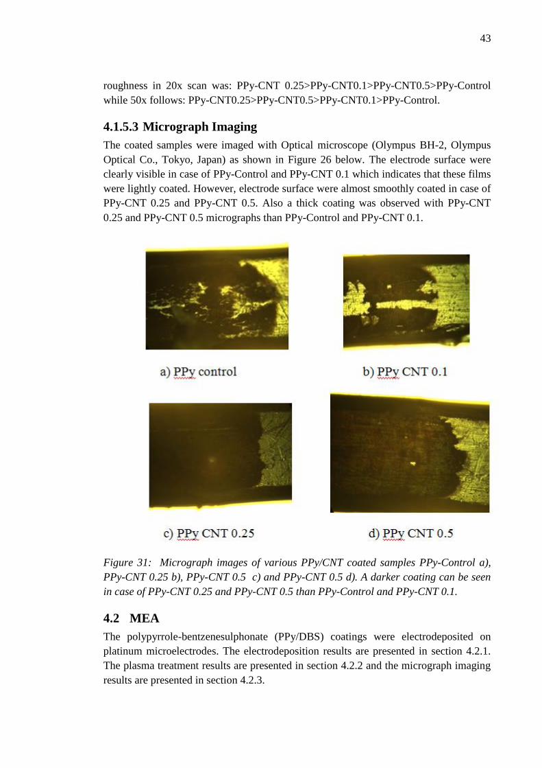
43
roughness in 20x scan was: PPy-CNT 0.25>PPy-CNT0.1>PPy-CNT0.5>PPy-Control
while 50x follows: PPy-CNT0.25>PPy-CNT0.5>PPy-CNT0.1>PPy-Control.
4.1.5.3 Micrograph Imaging
The coated samples were imaged with Optical microscope (Olympus BH-2, Olympus
Optical Co., Tokyo, Japan) as shown in Figure 26 below. The electrode surface were
clearly visible in case of PPy-Control and PPy-CNT 0.1 which indicates that these films
were lightly coated. However, electrode surface were almost smoothly coated in case of
PPy-CNT 0.25 and PPy-CNT 0.5. Also a thick coating was observed with PPy-CNT
0.25 and PPy-CNT 0.5 micrographs than PPy-Control and PPy-CNT 0.1.
Figure 31: Micrograph images of various PPy/CNT coated samples PPy-Control a),
PPy-CNT 0.25 b), PPy-CNT 0.5 c) and PPy-CNT 0.5 d). A darker coating can be seen
in case of PPy-CNT 0.25 and PPy-CNT 0.5 than PPy-Control and PPy-CNT 0.1.
4.2 MEA
The polypyrrole-bentzenesulphonate (PPy/DBS) coatings were electrodeposited on
platinum microelectrodes. The electrodeposition results are presented in section 4.2.1.
The plasma treatment results are presented in section 4.2.2 and the micrograph imaging
results are presented in section 4.2.3.

44
4.2.1 Electrodeposition
Linear Scan Voltammetry technique was used to ramp the voltage from an intial
potential to the final potential with the given scan rate. The final potential was then
fixed with certain charge limits to generate the current waveform by
chronopotentiometry technique. The area of one electrode in MEA was 0.707*10-5cm2.
This value was fitted to get the desired density curves. Also some of the curves are not
drawn to the ''end'' because the electrodeposition process was stopped because of
unstable negative current. The settings is given in Table 6 below.
Table 6: Settings for electrodeposition of PPy/DBS coatings
Electrodes E17 E54 E47 E52 E62 E73 E65
Initial potential (V) 0 0 0 0 0 0 0
Final potential (V) 1.0 1.0 1.5 1.0 1.3 1.5 1.5
Scan rate (V/s) 0.2 0.2 0.5 0.2 0.2 0.5 0.5
Charge limit (C/cm2)
7.07 7.07 7.07 7.07 7.07 7.07 7.07

45
a)
b)
Figure 32: Charge a) and current b) densities during electrodeposition.
0 100 200 300-2,5
0
2,5
5,0
7,5
10,0
Time (Sec)
Q (C
oulom
bs/cm
2 )E17.parE54.parE47.parE52.parE62.parE73.parE65.par
0 100 200 300-0,1
0
0,1
0,2
0,3
Time (Sec)
I (Amp
s/cm2 )
E17.parE54.parE47.parE52.parE62.parE73.parE65.par

46
We varied the final potential and scan rate of the electrodeposition to test their effect on
the electrodeposition process. It was clear from charge density curve that E54 and E47
seemed to be coated for longer duration until 275sec. E62 was found to be coated for
shortest of time until70sec. E65 showed similar response as E62. Charge density
reached peak with E52 within 70sec which is quickest among any other electrodes.
From the current density curve, it was seen that the current was unstable. E54 and E73
showed a large positive current while E17 and E65 showed a negative current within a
few milliseconds. Only E54 showed positive current values. No coating of the
electrodes were observed which was confirmed by micrograph image and unstable
negative current during the polymerization process.
However, variations in the charge and current density was significantly high. E52 had
the maximum charge and current density of approximately 7.81C/ cm2 and 0.26A/ cm2
respectively while E62 had the minimum charge and current density values of 3.32C/
cm2 and 0 .14A/ cm2 respectively. We tried to overcome the problem of unstable
negative current during the process by connecting a shunt resistor in the circuit with
electrodeposition settings as shown in Table 6 above. However, negative current were
still observed with no coating of the electrodes as shown in Figure 27 above.
4.2.1.1 The effect of shunt resistor on electrodeposition process
We used adjustable shunt resistor to overcome the problem of unstable negative current.
We used the resistor of 0.5MOhm and 1.0MOhm with charge limits as shown in Table 7
below. The obtained charge and current densities are shown in Fig 28 below.
Table 7: Settings for electrodeposition of PPy/DBS coatings (shunt resistor).
Resistor (MOhm) 0 0 0.5 1.0
Initial potential (V) 0 0 0 0
Final potential (V) 1.0 1.5 1.5 1.5
Scan rate (V/s) 0.5 0.5 0.5 0.5
Charge limit (C/cm2)
7.07 7.07 7.07 7.07

47
a)
b)
Figure 33: The effect of shunt resistor on electrodeposition process. Charge a) and
current b) densities during electrodeposition with and without adjustable shunt resistor.
0 50 100 150 200-2,5
0
2,5
5,0
7,5
Time (Sec)
Q (C
oulom
bs/cm
2 )E55 no resistor at 1.5V.parE55 no resistor at 1V.parE55 R=0.5 MOhm at 1.5V.parE55 R=1 MOhm at 1.5V.par
0 50 100 150 200-0,10
-0,05
0
0,05
0,10
0,15
Time (Sec)
I (Amp
s/cm2 )
E55 no resistor at 1.5V.parE55 no resistor at 1V.parE55 R=0.5 MOhm at 1.5V.parE55 R=1 MOhm at 1.5V.par

48
As seen from charge density curve, the maximum charge density was found with no
shunt resistor at 1.5V while with no resistor at 1.0V showed least charge density. Higher
resistor value of 1.0MOhm showed higher charge density with longer time duration
(160sec) than resistor value of 0.5MOhm, which showed time duration of 40sec. As
seen from current density curve, the current values were negative for all
electrodeposition. The deposition without resistor at 1.5 V had maximum positive and
negative current.
4.2.1.2 The effect of used voltage on electrodeposition process
Since no coating of the electrodes were observed with adjustable shunt resistor, we used
further more, different final potentials of 0.9V and 2V along with different charge limits
values as shown in above Table 8 to lower the negative current. However, the negative
current prevailed in the system with no coating of the electrodes as shown in Figure 29
below.
Table 8: Settings for electrodeposition of PPy/DBS coatings (higher potential).
Electrode E33 E33
Initial potential (V) 0 0
Final potential (V) 0.9 2
Scan rate (V/s) 0.5 0.5
Charge limit(C/cm2 ) 0.14 1.41

49
a)
b)
Figure 34: The effect of used voltage on electrodeposision process. Charge a) and
current b) densities during electrodeposition of a single microelectrode (E33) at a
voltage of 0.9V and 2V.
0 25 50 75-0,1
0
0,1
0,2
0,3
0,4
0,5
Time (Sec)
Q (C
oulom
bs/cm
2 )
E33 at 0.9V.parE33 at 2V first coat.parE33 at 2V second coat.par
0 25 50 75-0,02
-0,01
0
0,01
0,02
0,03
Time (Sec)
I (Amp
s/cm2 )
E33 at 0.9V.parE33 at 2V first coat.parE33 at 2V second coat.par

50
As seen from charge density curve, electrode coated at lower potential reached
maximum charge density while at higher volt couldn't reach at first coat (0.16Q/cm²).
However, at the second coat the charge density was risen until 0.45Q/cm² and then
decreases. From the current density curve, it was seen that all the electrodeposition
showed negative current. The coating at lower potential showed maximum positive and
maximum negative values of current density.
4.2.2 Impedance measurements
Pt MEA L1133 was plasma treated and then polymerized. The MEA-IT device was
used to measure the impedance at 1.0 kHz of microelectrodes before plasma treatment,
after plasma treatment and after polymerization. The measurements of plasma treated
plate were done at three time points (30mins, 1h and 2h) after plasma treatment.
4.2.2.1 The effect of plasma treatment on electrode impedance
The impedance of the microelectrode before and after plasma treatment were measured.
A significant decrease in impedance magnitude values were observed after plasma
treatment. The initial impedance magnitude of the MEA plate was around 80220kOhm
before the plasma treatment. The decrease in impedance magnitude was almost four
times, around 21800kOhm, when measured after 30 minutes after plasma treatment.
Similarly, the impedance was 9530kOhm and 480kOhm after one and two hours of
plasma treatment respectively as shown in Figure 30 below. The standard error before
plasma treatment was around ±441310kOhm. The standard errors after 30mins, 1h and
2h of plasma treatment were around ±42460kOhm, ±29330kOhmn and ±50kOhm
respectively.

51
a)
b)
Figure 35: The effect of plasma treatment on the microelectrode plate impedance
Impedance magnitude a) and phase b) at the frequency of 1.0 kHz before plasma
treatment and after plasma treatment.
0
20000
40000
60000
80000
100000
120000
140000
Before plasmatreatment
After plasmatreatment (30
min)
After plasmatreatment (1 h)
After plasmatreatment ( 2h)
Ave
rage
imp
edan
ce|Z
| (k
Oh
m)
0
10
20
30
40
50
60
70
80
90
100
Before plasmatreatment
After plasmatreatment( 30mins)
After plasmatreatment( 1 h)
After plasmatreatment(2 h)
Ave
rage
Ph
ase(ϴ
)

52
The phase angle was almost constant with approximately 67° until the last time point of
measurement. However, the phase angle was higher, 80°, when measured after 2h with
a large decrease in impedance values shown in Figure. The standard error before
plasma treatment was ±23°. The standard errors after 30mins, 1h and 2h of plasma
treatment were ±21°, ±20° and ±2° respectively. It was seen that the plasma treatment
had completely stabilized the electrode impedance after 2 hours as seen in Figure 31 a)
below. The phase angle was maximum after 2 hours of treatment as seen from Figure 31
b). However, not much difference in phase angle was seen after 30mins and 1h of
treatment.
a)
b)
Figure 36: The effect of plasma treatment on the microelectrode impedance: Impedance
magnitude a) and phase b) at the frequency of 1.0 kHz before plasma treatment and
after plasma treatment.
0
20000
40000
60000
80000
100000
120000
Before plasmatreatment
After plasmatreatment(30mins)
After plasmatreatment (1h)
After plasmatreatment (2h)
Ave
rage
imp
edan
ce|Z
| (k
Oh
m)
E44
E54
E64
0
10
20
30
40
50
60
70
80
90
Before plasmatreatment
After plasmatreatment(30mins)
After plasmatreatment (1h)
After plasmatreatment (2h)
Ave
rage
Ph
ase
(ϴ)
E44
E54
E64

53
The impedance of the individual electrodes were measured before and after plasma
treatment as shown in Figure 31. The impedance magnitude of E44 before plasma
treatment was 106000kOhm. The magnitude was almost half, around530kOhm when
measured after 2h of plasma treatment. The magnitude were around 610kOhm and
640kOhm after 30mins and 1h of plasma treatment respectively. The impedance
magnitude of E54 before plasma treatment was 2920kOhm. The magnitude was
470kOhm when measured after 2h of plasma treatment. The magnitude after 30mins
and 1h of plasma treatment were 670kOhm and 690kOhm respectively. The impedance
magnitude of E64 before plasma treatment was 106000kOhm. The magnitude was
510kOhm when measured after 2h of plasma treatment. The magnitude after 30mins
and 1h of plasma treatment were both same, 106000kOhm.
The phase angle of E44 before plasma treatment was 75°. The magnitude was 80°
when measured after 2h of plasma treatment. The magnitude were 81° and 82° after
30mins and 1h of plasma treatment respectively. The impedance magnitude of E54
before plasma treatment was 75°. The magnitude was 80° when measured after 2h of
plasma treatment. The magnitude after 30mins and 1h of plasma treatment were 81°
and 80° respectively. The impedance magnitude of E64 before plasma treatment was
65°. The magnitude was 81° when measured after 2h of plasma treatment. The
magnitude after 30mins and 1h of plasma treatment were 60° and 61° respectively.
4.2.2.2 The effect of electrodeposition on electrode impedances
The impedance of the individual electrodes E54, E54 and E64 were measured before
and after electrodeposition as shown in Figure 32 below. The impedance magnitude of
E44 before and after electrodeposition were 106000kOhm and 123kOhm respectively.
The impedance magnitude of E54 before and after electrodeposition were 2920kOhm
and 620kOhm respectively. The impedance magnitude of E64 before and after
electrodeposition were 106000kOhm and 93kOhm respectively.

54
a)
b)
Figure 37: Effect of electrodeposition on the electrode impedance: Impedance
magnitude a) and phase b) at the frequency of 1 kHz before polymerization and after
polymerization.
The phase angle of E44 before and after electrodeposition were 75° and 67°
respectively. The phase angle of E54 before and after electrodeposition were 75° and
72° respectively. Similarly, the phase angle of E64 before and after electrodeposition
were 65° and 68° respectively.
0
20000
40000
60000
80000
100000
120000
E44 E54 E64
Before polymerization
After polymerization
60
62
64
66
68
70
72
74
76
E44 E54 E64
Before polymerization
After polymerization

55
4.2.3 Micrograph Imaging
The micrograph images of the MEA plate after electrodeposition of electrodes E44, E54
and E 64 are shown below in Figure 33. It was hard to notice the coating on E44 as
seen in Fig 20 b). The electrode ''E44'' is shown by an arrow. Moreover, the electrolyte
solution looked to be spilled between the electrode gaps. It looked as if the plate and
electrodes were burned.
Figure 38: Micrograph imaging of MEA plates E44 (5x) a), E44 (10x) b), E54 and E64
(5x) c) and E54 and E64 (10x) d).
Likewise no coating of the electrodes were observed in E54 and E64 as seen in above
Figure 20 d). The electrodes numbers E54 and E64 are shown by an arrow.

56
5 DISCUSSION AND CONCLUSIONS
The general aim of this project was to coat the electrodes and to measure their electrical
properties and also to predict their surface roughness. The aim was also to measure the
electrical properties and to predict the roughness of the film by imaging or to observe
the effect of coating on the electrode surface.
Firstly, we performed electrochemical deposition of Pt microelectrode using different
scan rate of 0.2V/s and 0.5V/s and different final potential of 1.0V, 1.3V and 1.5V. We
selected some electrodes for the deposition process and applied different scan time and
final potential. No coating of the microelectrodes were observed with PPy solution
during the first trial. The polymerization currents were negative and some electrodes
even did not reach the maximum charge limit. We tried to overcome this problem by
changing the resistance in the circuit by connecting a potentiometer in the
electrochemical cell and by plasma treatment. The resistor values used was 0.5MOhm
and 1.0MOhm. We changed the scan potential to 0.5V/s and final potential to 1.0V and
1.5V. However, the negative current was still observed. At the third time, we tried to
coat the electrodes at higher volts, 2V and also by plasma treatment. But we were not
able to get the positive current and we were not able to coat the electrodes.
The plasma treatment was very effective in reducing the electrode impedance however
it did not help in coating of the electrodes. The reduction in impedance of plasma
treated film were almost only few hundred kOhm compared to impedance of thousands
of kOhm of untreated microelectrode plate. The plasma treated plates were also
compared with the polymerized plate. A major decrease in impedance magnitude was
observed with microelectrodes coating on electrode number 44 (E44) and 54 (E54) at all
time points and after electrodeposition process with only few hundred kOhm as shown
in Figure 19. The measured phase angle of E44 and E54 looked quite close at each
measurement phase with the highest value being close to 80°. The lowest value
observed was around 54° with E64. No such measurement for microelectrode has been
done before.
We then tried to coat the Pt macroelectrode with PPy and PPy/CNT solutions. We
successfully coated the macroelectrode with PPy and PPy/MWCNT composite. Similar
coating of PPy-MWCNT composite by electrochemical deposition was also observed in
previous research (Shaffer et al. 1998; Han et al. 2005; Almohsin et al. 2012; Li &
Zhitomirsky2013). However, in this thesis, results were not very convincing as there
was variation and the small concentration of CNT did not improve the electrical
properties. However, high concentration of CNT was successful in improving the
electrical properties of the coated electrode. The surface properties of PPy changed with
the addition of CNT. The PPy/CNT composition produced a more rougher film than the
PPy alone. Higher concentration of CNT (PPy-CNT 0.5) film was almost five times
more rougher than just PPy film as observed with AFM imaging. The increase in
surface roughness with addition of CNT was also observed in previous research
57
(Almohsin et al. 2012) (Shi & Zhitomirsky 2013). Some previous research showed that
the increase in surface roughness of coated electrode contributed to the increase in
resistive impedance of the electrode (Xiao et al. 2004) (Cui et al. 2001).
Similarly, the lowest roughness was observed with PPy-Control film as observed with
Optical Profilometry. The difference in roughness between PPy and PPy-CNT 0.25
surface was about 45.4µm in 20x scan and 10.9µm. This suggests that the PPy/CNT
composite could be useful to produce a rougher electrode surface. This could be of great
importance in the future research to predict the electrical behaviour of the electrode-
electrolyte interface. This might also help to have a better underestanding of the role of
CNT and PPy/CNT in electrochemical deposition. However, some variation in
chronopotentiometry measurement in this project was observed which might help to
motivate such coating in the future. Overall, this study highlights that the
macroelectrode was easily coated than microelectrodes.

58
6 APPENDIX
Table 9: Pre-treatment of microelectrodes. "-" indicates that no information is given
about the subject in the source.
Electrode/Area
Pre-treatment
of monomer pre-treatment of MEAs References
Au sites(neural
probe)/1250µm²
monomer
purged
with N2 for 5
mins. -
(Cuiet al.
2003)
Au/Ir
1250or3900µm²(neural
probe)
monomer
purged with
N2 for 5
mins. -
(Cui et al.
2001)
Au/1250 µm² (neural
probe)
monomer
purged with
N2 for 10
mins.
The probes are degreased
in acetic acid (5%), then
rinsed several times with
water and acetone before
electrochemical
deposition.
(Yang &
Martin
2004)
Au/1250 or 3900µm²
(neural probe)/
16 channel MEAs.
monomer
purged with
N2 for 5 mins.
The probes were cleaned
for 5 min at 80°C in a base
solution containing 1 part
ammonium hydroxide, 1
part 30% hydrogen
peroxide, and 5 parts
deionized water.
(Cui et al.
2001)
36 Au microelectrodes
area
degassed by
nitrogen
stream for
PSS and
pyrole -
(Ge et al.
2009)
1.6*10-3cm²/Pt
Pyrole was
purified by
distillation
under reduced
pressure
substrate treated with
alkysilane.
(Nishizawa
et al. 2007)

59
7 REFERENCES
Abidian, M. R., Kim, D. H., & Martin, D. C. (2006). Conducting polymer nanotubes for
controlled drug release. Adv. Mater. (18), 405–409.
Abidian, M. R., Ludwig, K. A., Marzullo, T. C., Martin, D. C., & Kipke, D. R. (2009).
Interfacing conducting polymer nanotubes with the central nervous system. Adv.Mater
(21), 3764–3770.
Abidian, M. R., & Martin, D. C. (2007). Experimental and theoretical characterization
of implantable neural microelectrodes modified with conducting polymer nanotubes. In
Biomaterials. Elsevier.
Abidian, M. R., & Martin, D. C. (2009). Multifunctional nanobiomaterials for neural
interfaces. Adv. Funct. Mater. (19), 573-585.
Abidian, M. R., Sales, L. G., Yazdan-Shahmorad, A., Marzullo, T. C., & Martin, D. C.
(2007). In vivo evaluation of chronically implanted neural microelectrode arrays
modified with poly(3,4-ethylenedioxythiophene) nanotubes. . In Proc. 3rd Int.
IEEE/EMBS Conf. on Neural Engineering, (pp. 61-64). Kohala Coast: HI.
Agui, L., Yanez-Sedeno, P., & Pingarron, J. M. (2008). Role of carbon nanotubes in
electroanalytical chemistry A review. analytica chimica acta, 62, 11–47.
Agui, L., Yanez-Sedeno, P., & Pingarron, J. M. (2008). Role of carbon nanotubes in
electroanalytical chemistry A review. analytica chimica acta (622), 11-47.
Almohsin, S. A., AL-Mutoki, S. M., & Li, Z. (2012). Electrochemical Polymerization of
PPy-MWCNT composite as a Counter Electrode for Dye-sensitized Solar Cells. Journal
of the Arkansas Academy of Science, 66, 31-35.
Ayoub, A., C, S. K., Sahito, I. A., & Jeong, S. H. (2016). Fabrication of textile fabric
counter electrode using activated charcoal doped multi walled carbon nanotube hybrid
for dye sensitized solar cell. Journal of Materials Chemistry A, 4.
Baranauskas, G., Maggiolini, E., Castagnola, E., Ansaldo, A., Mazzoni, A., Angotzi, G.
N., et al. (2011). Carbon nanotube composite coating of neural microelectrodes
preferentially improves the multiunit signal-to-noise ratio. Journal of Neural
Engineering, 8.
Blau, A., Murr, A., Wolff, S., Sernagor, E., Medini, P., Iurilli, G., et al. (2011). Flexible,
all-polymer microelectrode arrays for the capture of cardiac and neuronal signals.
Biomaterials, 32, 1778-1786.

60
Caglar, B. (2017). Production of Carbon Nanotubes by PECVD and Their Applications
to Supercapacitors. Barcelona, Spain. Retrieved from
http://diposit.ub.edu/dspace/bitstream/2445/11122/1/5NanostructuredMaterials-Caglar-
Burak.pdf.
Chemical Derivatization of Microelectrode Arrays by Oxidation of Pyrrole and N-
Methylpyrrole: Fabrication of Molecule-Based Electronic Devices1984Journal of
American Chemical Society106247389-7396
Chidichimo, G., & Filippelli, L. (2010). Organic Solar Cells: Problems and
Perspectives. International Journal of Photoenergy , 1-12.
Cui, X., Hetke, J., Wiler, J., Anderson, D., & Martin, D. (2001). Electrochemical
deposition and chaarcaterization of conducting polymer polypyrole/PSS on
multichannel neural probes. Sensors and Actuators A, 93 (1), 8-18.
Cui, X., Lee, V. A., Raphael, Y., Wiler, J. A., Hetke, J. F., Anderson, D. J., et al.
(2001). Surface modification of neural recording electrodes with conducting
polymer/biomolecule blends. J Biomed Mater Res, 56 (2), 261-272.
Cui, X., Wiler, J., Dzaman, M., Altschuler, R. A., & Martin, D. C. (2003). In vivo
studies of polypyrrole/peptide coated neural probes. Biomaterials (24), 777-787.
Fei, E., & Brock, R. (2013). Online. https://snsf.stanford.edu/. Retrieved on January 5,
2017, from https://snsf.stanford.edu/equipment/:
https://snsf.stanford.edu/equipment/xsa/docs/Park%20XE-100%20User%20Manual.pdf
Foulds, N. C., & Lowe, C. R. (1986). Enzyme entrapment in electrically conducting
polymers. J. Chem. Soc. Faraday Trans., I (82), 1259-1264.
Frölich, R., Rzany, A., Riedmüller, J., Bolz, A., & Schaldach, M. (1996). Electroactive
coating of stimulating electrodes. J. Mat. Sci. Materials in Medicine, 7, 393-397.
Ge, D., Tian, X., Qi, R., Huang, S., Mu, J., Hong, S., et al. (2009). A polypyrrole-based
microchip for controlled drug release. Electrochimica Acta, 55 (1), 271-275.
George, P. M., LaVan, D. A., Burdick, J. A., Chen, C.-Y., Liang, E., & R, L. (2006).
Electrically Controlled Drug Delivery from Biotin-Doped Conductive Polypyrrole.
Advanced Materials, 18 (5), 577-581.
George, P. M., Lyckman, A. W., LaVan, D. A., Hegde, A., Leung, Y., Avasare, R., et
al. (2005). Fabrication and biocompatibility of polypyrrole implants suitable for neural
prosthetics. Biomaterials, 26 (17), 3511-3519.
Gerard, M., Chaubey, A., & Malhotra, B. D. (2002). Review. Application of conducting
polymers to biosensors. Biosensors & Bioelectronics, 17, 345–359.

61
Goh, M., Matsushita, S., & Akagi, K. (2009). From helical polyacetylene to helical
graphite: synthesis in the chiral nematic liquid crystal field and morphology-retaining
carbonisation. Chemical Society Reviews , 2466-2476 .
Han, G., Yuan, G., Shi, G., & Wei, F. (2005). Electrodeposition of
polypyrrole/multiwalled carbon nanotube. Thin Solid Films , 64-69.
Harris, A. R., Morgan, S., Chen, J., Kapsa, R. M., & Wallace, G. G. (2013). Conducting
polymer coated neural recording electrodes. Journal of Neural Engineering, 10 (1), 1-
16.
Harwood, G. W., & Pouton, C. W. (1996). Amperometric enzyme biosensors for the
analysis of drug and metabolites. Adv. Drug. Deliv. Rev. , 163-191.
Heim, M., Yvert, B., & Kuhn, A. (2012). Nanostructuration strategies to enhance
microelectrode array (MEA) performance for neuronal recording and stimulation.
Journal of Physiology, 106 (3-4), 137-145.
Heller, A. (1990). Electrical wiring of redox and enzymes. Acc. Chem. Res., 23, 128-
134.
Impedance Testing Device MEA-IT Manual (2013). Online. Reutlingen: Multi Channel
Systems MCS GmbH. Retrived on January 5
2017.https://www.multichannelsystems.com/sites/multichannelsystems.com/files/docu
ments/manuals/MEA_Manual.pdf
Indian Instutute of Technology (2010). Online. Retrieved on January 2017, from
http://vlab1.iitr.ac.in/: http://vlab1.iitr.ac.in/data/theory/ecg%20theory.pdf
Jacobs, C. B., Peairs, M. J., & Venton, B. J. (2010). Review: Carbon nanotube based
electrochemical sensors for biomolecules. Analytica Chimica Acta , 105-127.
Jangid, N. K., Chauhan, N., Ameta, R., & Meghwal, K. (2014). A Review: Conducting
Polymers and Their Applications. . Research Journal of Pharmaceutical, Biological and
Chemical Sciences , 383-412.
Keefer, E. W., Botterman, B. R., Romero, M. I., Rossi, A. F., & Gross, G. W. (2008,
June 29). Carbon nanotube coating improves neural recordings. Article in Nature
Nanotechnology , pp. 1-6.
Kozai, T. D., Langhals, N. B., Patel, P. R., Deng, X., Zhang, H., Smith, K. L., et al.
(2012). Ultrasmall implantable composite microelectrodes with bioactive surfaces for
chronic neural interfaces. Nature Materials, 11, 1065-1073.
Kuncel, A. M., & Grill, W. M. (2004). Selection of stimulus parameters for deep brain
stimulation. Clinical Neurophysiology, 115 (11), 2431–2441.
62
LaVan, D. A., George, P. M., & Langer, R. (2003). Simple, three-dimensional
microfabrication of electrodeposited structures. Angew Chem, 42 (11), 1262–5.
Li, W., & J, T. (2010). Online.http://ralphgroup.lassp.cornell.edu/index.html. Retrieved
on March 19, 2017, from http://ralphgroup.lassp.cornell.edu/index.html:
http://ralphgroup.lassp.cornell.edu/projects/graphene_electrochemistry/
Li, X., & Zhitomirsky, I. (2013). Electrodeposition of polypyrroleecarbon nanotube
composites for electrochemical supercapacitors. Journal of Power Sources, 221, 49-56.
Li, Y. (2015). Organic Optoelectronic Materials. Suzhou 215123: Springer International
Publishing Switzerland 2015.
Lu, Y., Li, T., Zhao, X., Li, M., Cao, Y., Yang, H., et al. (2010). Electrodeposited
polypyrrole/carbon nanotubes composite films electrodes for neural interfaces.
Biomaterials, 31, 5169-5181.
Marcel, B. (2003). http://www.ece.umd.edu. Retrieved on January 3, 2017, from
http://www.ece.umd.edu/MEMS/resources/sop/:
http://www.ece.umd.edu/MEMS/resources/sop/VEECO_SOP.pdf
McCreery, D., Agnew, W. F., Yuen, T. G., & Bullara, L. (1990). Charge density and
charge per phase as cofactors in neural injury induced by electrical stimulation. EEE
Transactions on Biomedical Engineering, 37 (10), 996–1001.
McQuade, D. T., Pullen, A. E., & Swager, T. M. (2000). Conjugated polymer-
basedchemicalsensors. Chem. Rev., 100 (7), 2537–2574.
Merkoci, A., Pumera, M., Llopis, X., Perez, B., Valle, M. D., & S, A. (2009). New
materials for electrochemical sensing VI: Carbon nanotubes. Trends in Analytical
Chemistry , 9.
Merrill, D. R., Bikson, M., & R, J. J. (2005). Electrical stimulation of excitable tissue:
design of efficacious and safe protocols. Journal of Neuroscience Methods, 141 (2),
171-198.
Microporous conducting polymers on neural microelectrode arrays I Electrochemical
deposition.2004.Sensors and Actuators B1011-2133-142
Neuman, M. R. (2000). The Biomedical Engineering Handbook: Second Edition. Boca
Raton: CRC Press LLC.
Nishizawa, M., Nozaki, H., Kaji, H., Kitazume, T., Kobayashi, N., Ishibashi, T., et al.
(2007). Electrodeposition of anchored polypyrrole film on microelectrodes and
stimulation of cultured cardiac myocytes. Biomaterials, 28 (8), 1480-1485.
Otero, T. F., & Sansinena, J. M. (1998). Soft and wet conducting polymers for artificial
muscles. Adv. Mater. (10), 491–494.

63
Paul, E. W., Ricco, A. J., & Wrighton, M. S. (1985). Resistance of polyaniline films as a
function of electrochemical potential and the fabrication of polyaniline-based
microelectronic devices. J. Phys.Chem., 89, 1441–1447.
Ravichandran, R., Sundarrajan, S., Venugopal, J. R., Mukherjee, S., & Ramakrishna, S.
(2010). Applications of conducting polymers and their issues in biomedical engineering.
J. R. Soc. Interface , S559–S579.
Riistama, J. (2010). Characterization of wearable and mplantable Physiological
Measurement Devices. Tampere University of Technology .
Sarac, A. S., Ates, M., & Kilic, B. (2008). Electrochemical Impedance Spectroscopic
Study of Polyaniline on Platinum, Glassy Carbon and Carbon Fiber Microelectrodes.
Int. J. Electrochem. Sci, 3, 777 - 786.
Schmidt, C. E., Shastri, V. R., Vacanti, J. P., & Langer, R. (1997). Stimulation of
neurite outgrowth using an electrically conducting polymer. Proc. Natl Acad. Sci. (94),
8948–8953.
Schultze, J. W., & Karabulut, H. (2005). Application potential of conducting polymers.
Electrochim. Acta, 50, 1739–1745.
Shaffer, M. S., Fan, X., & Windle, A. H. (1998). Dispersion and Packaging of
carbonnanotubesCarbon , 1603-1612.
Shannon, R. V. (1992). A model of safe levels for electrical stimulation. IEEE Trans
Biomed Eng, 39 (4), 424-6.
Shi, C., & Zhitomirsky, I. (2013). Electrodeposition of composite polypyrrole–carbon
nanotube films. Surface Engineering , 655-661.
Sloten, J. V., Nyssen, V. M., & Haueisen, J. (2008). Coating of neural microelectrodes
with intrinsically conducting polymers as a means to improve their electrochemical
properties . IFMBE Proceedings 22 (pp. 2409–2412). Berlin: Springer-Verlag.
Stonecypher, L. (2011). Online. http://www.brighthubengineering.com. Retrieved on
January 5, 2017, from http://www.brighthubengineering.com/manufacturing-
technology/: http://www.brighthubengineering.com/manufacturing-technology/95102-
atomic-force-microscopy-afm-contact-non-contact-and-semi-contact-modes/
The Membranes Research Environment (2009). Online.http://membranes.edu.au.
Retrieved on January 6, 2017, from
http://membranes.edu.au/wiki/index.php/Surface_Roughness:
http://membranes.edu.au/wiki/index.php/Surface_Roughness
The Royal Society of Chemistry (2015). Online. http://www.chemspider.com. Retrieved
on January 8, 2017, from http://www.chemspider.com/Chemical-

64
Structure.10606193.html: http://www.chemspider.com/Chemical-
Structure.10606193.html
The Royal Swedish Academy of Sciences: The Nobel Prize in Chemistry, 2000:
Conductive Polymers, Advanced Information, Stockholm (2000)
Towards real world applications: reproducible and stable PEDOT-CNT
microelectrodes.2012.8th Int. Meeting on Substrate-Integrated Microelectrode Arrays,
2012327-328DeizisauIVS Abele GmbH
Unwin, P. R., & Bard, A. J. (1992). Ultramicroelectrode voltammetry in a drop of
solution: a new approach to the measurement of adsorption isotherms at solid–liquid
interface. Anal. Chem., 64, 113-119.
Vairavapandian, D., Vichchulada, P., & Lay, M. D. (2008). Preparation and
modification of carbon nanotubes: Review of recent advances and applications
incatalysis and sensing. analytica chimica acta, 626, 119-129.
Vidal, J.-C., Garcia-Ruiz, E., & Castillo, J.-R. (2003). Recent Advances in
Electropolymerized Conducting Polymers. Microchim. Acta, 143 (2), 93-111.
Vidu, R., Rahman, M., Mahmoudi, M., Enachescu, M., Poteca, T. D., & Opris, L.
(2014). Nanostructures: a platform for brain repair and augmentation. Frontiers in
Systems Neuroscience, 8, 1-24.
Volder, M. F., Tawfick, S. H., Baughman, R. H., & Hart, A. J. (2013). Carbon
Nanotubes: Present and Future Commercial Applications. Science , 535-539.
Wadhwa, R., Lagenaur, C. F., & Cui, X. T. (2006). Electrochemically controlled release
of dexamethasone from conducting polymer polypyrrole coated electrode. Journal of
Controlled Release, 110, 531-561.
Weiland, J. D., & Anderson, D. J. (2000). Chronic neural stimulation with thin-film,
iridium oxide electrodes. IEEE Trans. Biomed. Eng, 47 (7), 911-918.
Woo, E. J. (2015). Online.http://www.ejwoo.com. Retrieved on March 2017, from
http://www.ejwoo.com/biomedical-instrumentation.html:
http://iirc.khu.ac.kr/uploads/6/3/4/3/63434825/ch05webster.pdf
Xiao, Y., Cui, X., & Martin, D. C. (2004). Electrochemical polymerization and
properties of PEDOT/S-EDOT on neural microelectrode arrays. Journal of
Electroanalytical Chemistry, 573, 43-48.
Xiao, Y., Cui, X., Hancock, J. M., Bouguettaya, M., Reynolds, J. R., & Martin, D. C.
(2004). Electrochemical polymerization of poly(hydroxymethylated-3,4-
ethylenedioxythiophene) (PEDOT-MeOH) on multichannel neural probes. Sensors and
Actuators B, 99 (2-3), 437-443.

65
Xu, L. B., Chen, W., Mulchandani, A., & Yan, Y. (2005). Reversible conversion of
conducting polymer films from superhydrophobic to superhydrophilic. . Angew. Chem.
Int. , 6009–6012. .
Yang, J., & Martin, D. C. (2004). Microporous conducting polymers on neural
microelectrode arrays II. Physical characterization. Sensors and Actuators, 113, 204-
211.
Yang, S. Y., Kim, N. H., Cho, Y. S., Lee, H., & Kwon, H. J. (2014). Convallatoxin, a
Dual Inducer of Autophagy and Apoptosis, Inhibits Angiogenesis. PLOS ONE, 9.
Zelikin, A. N., D, L., Farhadi, J., Martin, I., Shastri, V., & Langer, R. (2002). Erodible
conducting polymers for potential biomedical applications. Angew Chem, 41 (1), 141-4.
Zhong, Y. H., Yu, X. J., Gilbert, R., & Bellamkonda, R. V. (2001). Stabilizing
electrode-host interfaces: a tissue engineering approach. . Rehabil. J. Res. Dev. , 627–
632.
Ziadan, K. M. (2012). In A. D. Gomes, Conducting Polymers Application, New
Polymers for Special Applications. InTech.
Zygo Corporation (2017). Online. https://www.zygo.com. Retrieved March on 5, 2017,
from https://www.zygo.com/?/met/profilers:
https://www.zygo.com/?/met/profilers/opticalprofilersabout.htm
Copyright © 2022 FDOKUMEN