Study of composition dependent structural, optical, and magnetic properties of Cu-doped Zn1-xCdxS...
7
Study of composition dependent structural, optical, and magnetic properties of Cu-doped Zn 1-x Cd x S nanoparticles Amit Kumar Chawla, 1 Sonal Singhal, 1,2,3 Sandeep Nagar, 4 Hari Om Gupta, 2 and Ramesh Chandra 1,a 1 Nanoscience Laboratory, Institute Instrumentation Centre, Indian Institute of Technology Roorkee, Roorkee 247667, India 2 Department of Electrical Engineering, Indian Institute of Technology Roorkee, Roorkee 247667, India 3 Department of Mechanical Material and Manufacturing Engineering, University of Nottingham, NG7 2RD Nottingham, United Kingdom 4 Department of Material Science and Engineering, Royal Institute of Technology, SE-100 44 Stockholm, Sweden Received 17 May 2010; accepted 2 November 2010; published online 28 December 2010 Cu-doped Zn 1-x Cd x S nanoparticles were synthesized by coprecipitation technique in ice bath at 280 K. The band gap energy of Zn 1-x Cd x S:Cu nanoparticles can be tuned to a lower energy by increasing the Cd content, indicating the formation of the alloyed nanoparticles. The alloy structure is further supported by the systematic shifting of characteristic x-ray diffraction peaks to lower angles with increase in Cd content. Systematic copper doping induces a red shift in the energy band gap of Zn 0.9 Cd 0.1 S : Cu nanoparticles with increase in copper concentration. Cu-doped Zn 0.9 Cd 0.1 S nanoparticles were found to have ferromagnetic nature at 5 K whereas undoped particles were found to be diamagnetic. Green luminescence further proves proper doping of Cu into the ZnCdS matrix. It is believed that the green luminescence originates from the recombination between the shallow donor level sulfur vacancy and the t 2 level of Cu 2+ . This method provides an inexpensive and simple procedure to produce ternary ZnCdS:Cu nanoparticles with tunable optical properties via changing Cd and/or Cu concentrations. © 2010 American Institute of Physics. doi:10.1063/1.3524516 I. INTRODUCTION Semiconductor nanoparticles have generated great fun- damental and technical interest due to novel size-tunable properties and, consequently, in potential applications as op- toelectronic devices and biomedical tags. 1–3 In the past two decades, the main efforts have been focused on the prepara- tion of different color-emitting binary or core-shell nanocrys- tals with different particle sizes 1,4 using simple and inexpen- sive chemical routes. However, the tuning of physical and chemical properties by varying the particle size could cause problems in many applications, in particular, if unstable small particles less than 2 nm are used. 5 Apart from binary compositions, exploration of tunable optical properties of ter- nary compositions has become an alternative way to produce desired wavelength by changing their stoichiometries and/or doping. 6 Yang and co-workers reported ternary Zn x Cd 1-x Se alloyed nanocrystals with luminescent properties comparable or even better than the best-reported binary CdSe based nanocrystals. 7 We have reported earlier a simple method to manufacture ZnCdS nanoparticles with size tunable properties. 8 Semiconducting nanoparticles, especially sul- fides doped with transition metal ions and rare-earth ions, have been studied extensively because of their excellent lu- minescence properties. 9,10 The optical properties of doped nanomaterials differ from the corresponding host nanomate- rials as the dopants form deep trap levels and act as lumines- cence centers. 11,12 Discrete energy states can be introduced in the band gap of semiconducting host by doping with transi- tion metals such as Cu, Ag and Mn. 13 In this regard, the role of Cu as a luminescence activator is of considerable signifi- cance for II-VI compound semiconductors. There have been number of research groups investigating Cu-doped ZnS nanoparticles by chemical routes. Datta et al. investigated the effect of Cu incorporation on the phase transition from wrutzite to Cubic structure prepared by solvothermal process. 14 Geng et al. have reported the synthesis of ZnS:Cu 2+ nanorods through a solution phase thermal de- composition molecule precursor route. They were able to tune the optical properties of the products by changing Cu doping concentration. 15 Unni et al. synthesize the CdS, CdS:Zn 2+ and CdS:Cu 2+ and reported the photolumines- cence quenching at 15 wt % of Cu. 16 Bol et al. have ob- served the red emission in addition to the green emission in the PL spectra of Cu doped ZnS nanoparticles. 12 Lowest syn- thesis temperature considered by other research workers is 300 K. Peng et al. 13 have reported the synthesis and photo- luminescence properties of Cu doped ZnS nanoparticles via chemical route at 300 K. The highest temperature reported in the literature have gone up to 900–1000 °C. These elevated temperatures are the firing temperature and are applied when nanoparticles found their application in nanophosphor. Nien et al. 17 have reported the red electroluminescent phosphor powders synthesized via chemical route and then subjected to the firing temperature of 900 ° C. Recently Kim et al. have shown the successful formation of transition metal doped Zn 1-x Cd x S nanoparticles at room temperature. 18,19 a Electronic mail: ramesfi[email protected]. JOURNAL OF APPLIED PHYSICS 108, 123519 2010 0021-8979/2010/10812/123519/7/$30.00 © 2010 American Institute of Physics 108, 123519-1 Downloaded 01 Jan 2011 to 210.212.58.229. Redistribution subject to AIP license or copyright; see http://jap.aip.org/about/rights_and_permissions
-
Upload
independent -
Category
Documents
-
view
2 -
download
0
Transcript of Study of composition dependent structural, optical, and magnetic properties of Cu-doped Zn1-xCdxS...
Study of composition dependent structural, optical, and magneticproperties of Cu-doped Zn1−xCdxS nanoparticles
Amit Kumar Chawla,1 Sonal Singhal,1,2,3 Sandeep Nagar,4 Hari Om Gupta,2 andRamesh Chandra1,a�
1Nanoscience Laboratory, Institute Instrumentation Centre, Indian Institute of Technology Roorkee,Roorkee 247667, India2Department of Electrical Engineering, Indian Institute of Technology Roorkee, Roorkee 247667, India3Department of Mechanical Material and Manufacturing Engineering, University of Nottingham,NG7 2RD Nottingham, United Kingdom4Department of Material Science and Engineering, Royal Institute of Technology, SE-100 44 Stockholm,Sweden
�Received 17 May 2010; accepted 2 November 2010; published online 28 December 2010�
Cu-doped Zn1−xCdxS nanoparticles were synthesized by coprecipitation technique in ice bath at 280K. The band gap energy of Zn1−xCdxS:Cu nanoparticles can be tuned to a lower energy byincreasing the Cd content, indicating the formation of the alloyed nanoparticles. The alloy structureis further supported by the systematic shifting of characteristic x-ray diffraction peaks to lowerangles with increase in Cd content. Systematic copper doping induces a red shift in the energy bandgap of Zn0.9Cd0.1S :Cu nanoparticles with increase in copper concentration. Cu-doped Zn0.9Cd0.1Snanoparticles were found to have ferromagnetic nature at 5 K whereas undoped particles were foundto be diamagnetic. Green luminescence further proves proper doping of Cu into the ZnCdS matrix.It is believed that the green luminescence originates from the recombination between the shallowdonor level �sulfur vacancy� and the t2 level of Cu2+. This method provides an inexpensive andsimple procedure to produce ternary ZnCdS:Cu nanoparticles with tunable optical properties viachanging Cd and/or Cu concentrations. © 2010 American Institute of Physics.�doi:10.1063/1.3524516�
I. INTRODUCTION
Semiconductor nanoparticles have generated great fun-damental and technical interest due to novel size-tunableproperties and, consequently, in potential applications as op-toelectronic devices and biomedical tags.1–3 In the past twodecades, the main efforts have been focused on the prepara-tion of different color-emitting binary or core-shell nanocrys-tals with different particle sizes1,4 using simple and inexpen-sive chemical routes. However, the tuning of physical andchemical properties by varying the particle size could causeproblems in many applications, in particular, if unstablesmall particles �less than 2 nm� are used.5 Apart from binarycompositions, exploration of tunable optical properties of ter-nary compositions has become an alternative way to producedesired wavelength by changing their stoichiometries and/ordoping.6 Yang and co-workers reported ternary ZnxCd1−xSealloyed nanocrystals with luminescent properties comparableor even better than the best-reported binary CdSe basednanocrystals.7 We have reported earlier a simple method tomanufacture ZnCdS nanoparticles with size tunableproperties.8 Semiconducting nanoparticles, especially sul-fides doped with transition metal ions and rare-earth ions,have been studied extensively because of their excellent lu-minescence properties.9,10 The optical properties of dopednanomaterials differ from the corresponding host nanomate-rials as the dopants form deep trap levels and act as lumines-cence centers.11,12 Discrete energy states can be introduced in
the band gap of semiconducting host by doping with transi-tion metals such as Cu, Ag and Mn.13 In this regard, the roleof Cu as a luminescence activator is of considerable signifi-cance for II-VI compound semiconductors. There have beennumber of research groups investigating Cu-doped ZnSnanoparticles by chemical routes. Datta et al. investigatedthe effect of Cu incorporation on the phase transition fromwrutzite to Cubic structure prepared by solvothermalprocess.14 Geng et al. have reported the synthesis ofZnS:Cu2+ nanorods through a solution phase thermal de-composition molecule precursor route. They were able totune the optical properties of the products by changing Cudoping concentration.15 Unni et al. synthesize the CdS,CdS:Zn2+ and CdS:Cu2+ and reported the photolumines-cence quenching at 15 wt % of Cu.16 Bol et al. have ob-served the red emission in addition to the green emission inthe PL spectra of Cu doped ZnS nanoparticles.12 Lowest syn-thesis temperature considered by other research workers is300 K. Peng et al.13 have reported the synthesis and photo-luminescence properties of Cu doped ZnS nanoparticles viachemical route at 300 K. The highest temperature reported inthe literature have gone up to 900–1000 °C. These elevatedtemperatures are the firing temperature and are applied whennanoparticles found their application in nanophosphor. Nienet al.17 have reported the red electroluminescent phosphorpowders synthesized via chemical route and then subjectedto the firing temperature of 900 °C. Recently Kim et al. haveshown the successful formation of transition metal dopedZn1−xCdxS nanoparticles at room temperature.18,19a�Electronic mail: [email protected].
JOURNAL OF APPLIED PHYSICS 108, 123519 �2010�
0021-8979/2010/108�12�/123519/7/$30.00 © 2010 American Institute of Physics108, 123519-1
Downloaded 01 Jan 2011 to 210.212.58.229. Redistribution subject to AIP license or copyright; see http://jap.aip.org/about/rights_and_permissions
There have been few reports on Cu2+ doped Zn1−xCdxSnanoparticles20 at low temperature processing to obtain thegreen luminescence. To the best of our knowledge, there isno report on the Cu-doped Zn1−xCdxS nanoparticles using icebath synthesis. Thus, herein, we employed chemical route asan aqueous coprecipitation method to synthesize Cu-dopedZn1−xCdxS nanoparticles at relatively lower temperature andhave explored their composition dependent optical and struc-tural properties.
II. EXPERIMENT
Cu doped Zn1−xCdxS nanoparticles have been synthe-sized in the laboratory at 280 K using coprecipitation tech-nique in ice bath. Appropriate molar amount of zinc nitratehexahydrate, cadmium nitrate tetrahydrate, copper nitratehexahydrate, and sodium sulphide were taken to maintain thestoichiometry of the nanoparticles. In one set of experimentZn1−xCdxS �x=0.1, 0.2, 0.3, 0.4, and 0.5� nanoparticles wereprepared in a manner that the concentration of Cd is variedsuch that the mole fraction �x�, molar ratio of cadmium tozinc, varies in steps of 0.1 from 0.1 to 0.5 while keepingmolar amount of copper fixed at 0.005 M. In another experi-ment, Cd mole fraction �x� is kept constant at 0.1 with vary-ing Cu concentrations as 0.005, 0.01, and 0.015 M. In thetypical experiment requisite amounts of 0.5 M zinc nitrate,0.05 M cadmium nitrate and appropriate molar amount ofCopper nitrate aqueous solution were mixed. 0.5 M sodiumsulfide aqueous solution was added into the above mixturewith a dripping speed of ten drops per minute. Continuousstirring was also provided for better intermixing during thelength of the reaction at 280 K. The resulting precipitateswere filtered off and washed several times in distilled waterand acetone. The precipitates were dried in hot air oven at323 K.
Quantitative elemental analysis was performed by en-ergy dispersive spectrometer attached with FE-SEM �FEIQuanta 200 F�. The particle size and the shape of the nano-particles were determined by transmission electron micros-copy �FEI TECNAI-G2�. X-ray analysis was performed byusing a Diffractometer with Cu K� target �Bruker D8 Ad-vance� radiation. Optical absorption was measured in the200–800 nm wavelength range using UV-Vis-NIR spectro-photometer �Cary 5000 Varian�. For absorbance measure-ment the nanoparticles were dispersed in isopropyl alcohol.Isopropyl alcohol has its absorption wavelength at 204 nmand thus it becomes an attractive choice as solvent. In atypical measurement 2 mg of each nanoparticle was dis-persed in 50 ml Isopropyl alcohol and the solution was ul-trasonicated to prevent the precipitation of sample. A clearsolution thus obtained was used for the measurement. Forobtaining the absorption characteristics of all the samples, atfirst the transmittance �T� at different wavelengths ��� aremeasured and then absorbance ��� at the correspondingwavelengths � are calculated using the Beer–Lambert’s rela-tion,
� =1
dln� 1
T� ,
where d is the path length in centimeter. In our case the pathlength considered was 1 cm. Photoluminescence emissionspectra were recorded at room temperature with a photolu-minescence spectrometer �Perkins Elmer LS 55�. Magneticmeasurements were taken with superconducting quantum in-terference device �SQUID� magnetometer �QD MPMS-XL�.
III. RESULTS AND DISCUSSIONS
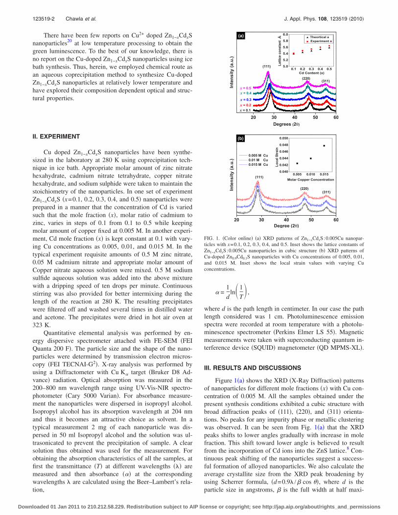
Figure 1�a� shows the XRD �X-Ray Diffraction� patternsof nanoparticles for different mole fractions �x� with Cu con-centration of 0.005 M. All the samples obtained under thepresent synthesis conditions exhibited a cubic structure withbroad diffraction peaks of �111�, �220�, and �311� orienta-tions. No peaks for any impurity phase or metallic clusteringwas observed. It can be seen from Fig. 1�a� that the XRDpeaks shifts to lower angles gradually with increase in molefraction. This shift toward lower angle is believed to resultfrom the incorporation of Cd ions into the ZnS lattice.8 Con-tinuous peak shifting of the nanoparticles suggest a success-ful formation of alloyed nanoparticles. We also calculate theaverage crystallite size from the XRD peak broadening byusing Scherrer formula, �d=0.9� /� cos ��, where d is theparticle size in angstroms, � is the full width at half maxi-
20 30 40 50 60
x = 0.3
x = 0.5x = 0.4
x = 0.2
(111)
(311)(220)
0.1 0.2 0.3 0.4 0.55.0
5.2
5.4
5.6
5.8
6.0
�������
��
���
��
Cd Content (x)
Theortical aExperiment a
���
��������
Degrees (2θ)
x = 0.1
(a)
20 30 40 50 60
0.005 0.010 0.0150.040
0.042
0.044
0.046
0.048
0.050
LocalStrain
Molar Copper Concentration
(311)(220)
(111)
Intensity(a.u.)
Degree (2θ)
0.005 M Cu0.01 M Cu0.015 M Cu
(b)
FIG. 1. �Color online� �a� XRD patterns of Zn1−xCdxS:0.005Cu nanopar-ticles with x=0.1, 0.2, 0.3, 0.4, and 0.5. Inset shows the lattice constants ofZn1−xCdxS:0.005Cu nanoparticles in cubic structure �b� XRD patterns ofCu-doped Zn0.9Cd0.1S nanoparticles with Cu concentrations of 0.005, 0.01,and 0.015 M. Inset shows the local strain values with varying Cuconcentrations.
123519-2 Chawla et al. J. Appl. Phys. 108, 123519 �2010�
Downloaded 01 Jan 2011 to 210.212.58.229. Redistribution subject to AIP license or copyright; see http://jap.aip.org/about/rights_and_permissions

mum �FWHM�, � is the wavelength of the x-rays used�=1.54 �.21 Particle sizes of 3.80 nm, 3.76 nm, 3.71 nm,3.67 nm, and 3.65 nm have been obtained for the mole frac-tion, x of 0.1, 0.2, 0.3, 0.4, and 0.5, respectively.
Semiconductor alloys �solid solutions� have been pro-posed to obey Vegard’s law,22 revealing the linear relation-ship between the lattice constant and composition as follows:
aA1−xBxC0 �x� = �1 − x�aAC
0 + xaBC0 , �1�
where aA1−xBxC0 is the natural constant of the ternary form
A1−xBxC and aAC0 and aBC
0 are the natural constants of thebinaries AC and BC, respectively, and x is the mole fractionof binary BC ranging from 0 to 1. In the case of CubicZn1−xCdxS nanoparticles, the ideal lattice constant with Cdconcentration of 0.05 M is 5.392 Å, where cubic aZnS
0
=5.345 Å �PDF # 80–0020� and aCdS0 =5.820 Å �PDF # 01–
0647�. Square data points in the inset of Fig. 1�a� correspondto lattice constants of Zn1−xCdxS with mole fractions in cubicstructure obtained from XRD data. The triangular data pointsare obtained by Vegard’s law using Eq. �1�. Vegard’s law wasapplied to check the compositional homogeneity of the semi-conductor nanoparticles. It can be seen from the inset of Fig.1�a� that there is a gradual increase in the lattice parameterwith increase in the mole fraction. This trend is consistentwith Vegard’s law and indicates a homogeneous alloy struc-ture. The close agreement between the experimental and thetheoretical lattice values also indicates that the compositionof the nanoparticles was very close to the mixing molar ratioof the starting materials of ZnS and CdS and it rules out thepossibility of a separate nucleation of CdS and ZnS.
Figure 1�b� shows the XRD patterns of the Zn0.9Cd0.1Snanoparticles with Cu concentrations of 0.005, 0.01, and0.015 M. Cubic structure with �111�, �220�, and �311� orien-tations were obtained. The average crystallite size came outto be 3.8, 3.6, and 3.5 nm for Cu-doped Zn0.9Cd0.1S nano-particles with Cu concentrations of 0.005, 0.01, and 0.015 M,respectively. It can be seen from Fig. 1�b� that there is aslight shift in the XRD peak position toward lower anglewith increase in Cu concentration. A shift in the d spacing isattributed to the strain produced in the lattice upon Cu incor-poration. Resulting strain in the lattice arises due to the dif-ferences in the ionic radii of Zn2+ �0.74 Å� and Cu2+ �0.72Å�.23 According to Hume Rothary rules for the formation ofsubstitutional solid solutions, the ionic radii of the solute andsolvent atoms must differ by no more than 15%. In thepresent case ionic radii difference is came to be around�2.7% which is fairly smaller than 15%, satisfying theHume–Rothary rule.24 This helps to rule out the possibilityof “Cu” ions coming out of the host lattice. Thus, one canclearly conclude that substitutional Cu-doping in Zn1−xCdxSlattice is accomplished. In order to find out the extent ofstrain that have been induced in the lattice due to copperincorporation, strain analysis has also been carried out. Localstrain is calculated by making use of Scherrer formula of �kversus k �the scattering vector k= �4� /��sin ��.25 The threepeaks of �111�, �220�, and �311� were fitted linearly to obtainthe local strain values. Calculated values of local strain are
shown in the inset of Fig. 1�b�. Local strain increases, asexpected, with increase in the copper concentration.
Figure 2 shows the ��hv�2 versus photon energy ofZn1−xCdxS:0.005Cu nanoparticles with the mole fraction.The red-shift in band gap from 3.95 to 3.43 eV with increas-ing mole fraction clearly indicates the formation of alloyednanoparticles also supporting the XRD data. We also devel-oped an equation with the input values as the experimentalband gap values obtained by absorption measurement. Figure3 shows the fit to the energy band gap values. Regressioncoefficient is found close to 1, signifies that the trend line fitsvery well to the experimental data points.
Eg�x� = 4.17 − 2.34x + 1.73x2; R2 = 0.998. �2�
Bowing parameter is the coefficient of the quadratic term ofthe above equation and has a value of 1.73.
In bulk CdS–ZnS alloyed crystals their composition �x�dependent bandgap energies �Eg�x�� can be expressed by therelation22
Eg�x� = Eg�ZnS� + �Eg�CdS� − Eg�ZnS� − b�x + bx2, �3�
where Eg�ZnS� and Eg�CdS� are the band gap energies forbulk ZnS �Eg=3.6 eV� and CdS �Eg=2.36 eV�, respec-tively, and b is the bowing parameter �bulk value for bowingparameter is 0.61�.26,27
In Fig. 4 calculated results for alloyed bulks �using Eq.�3�� and nanoparticles �using Eq. �2�� are shown as the dottedand solid lines, respectively. Using the calculated bandgapenergy �line curve� of Zn1−xCdxS:0.005Cu nanoparticles, theactual compositions of Zn1−xCdxS:0.005Cu nanoparticlescan be indirectly estimated. EDS results shows that the mole
3.0 3.2 3.4 3.6 3.8 4.0 4.20.0
0.1
0.2
0.3
0.4
0.5
x = 0.2x = 0.3x = 0.4x = 0.5
(�h�)2
h� (eV)
x = 0.1
FIG. 2. �Color online� ��hv�2 vs photon energy of Zn1−xCdxS:0.005Cunanoparticles with x=0.1, 0.2, 0.3, 0.4, and 0.5.
FIG. 3. �Color online� A polynomial fit to to the energy band gap valuesobtained from absorbance nmeasurement.
123519-3 Chawla et al. J. Appl. Phys. 108, 123519 �2010�
Downloaded 01 Jan 2011 to 210.212.58.229. Redistribution subject to AIP license or copyright; see http://jap.aip.org/about/rights_and_permissions
fraction �x� of 0.11�0.045, 0.22�0.038, 0.31�0.051,0.41�0.048, 0.52�0.049 are obtained for 0.1, 0.2, 0.3, 0.4,and 0.5, respectively.
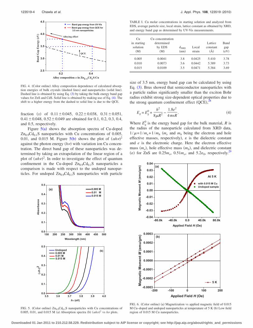
Figure 5�a� shows the absorption spectra of Cu-dopedZn0.9Cd0.1S nanoparticles with Cu concentrations of 0.005,0.01, and 0.015 M. Figure 5�b� shows the plot of ��h�2
against the photon energy �h� with variation ion Cu concen-tration. The direct band gap of these nanoparticles was de-termined by taking an extrapolation of the linear region of aplot of ��h�2. In order to investigate the effect of quantumconfinement in the Cu-doped Zn0.9Cd0.1S nanoparticles acomparison is made with respect to the undoped nanopar-ticles. For undoped Zn0.9Cd0.1S nanoparticles with particle
size of 3.5 nm, energy band gap can be calculated by usingEq. �3�. Brus showed that semiconductor nanoparticles witha particle radius significantly smaller than the exciton Bohrradius exhibit strong size-dependent optical properties due tothe strong quantum confinement effect �QCE�,28
Eg = Eg0 +
h2
8R2 −1.8e2
4��R. �4�
Where Eg0 is the energy band gap for the bulk material, R is
the radius of the nanoparticle calculated from XRD data,1 /=1 /me+1 /mh �me and mh being the electron and holeeffective masses, respectively�, � is the dielectric constantand e is the electronic charge. Here the electron effectivemass �me�, hole effective mass �mh�, and dielectric constant��� for ZnS are 0.25mo, 0.51mo, and 5.2�0, respectively.29
TABLE I. Cu molar concentrations in starting solution and analyzed fromEDS, average particle size, local strain, lattice constant as obtained by XRD,and energy band gap as determined by UV-Vis measurements.
Cuin startingsolution
�M�
Cu concentrationdetermined
by EDS�M�
dXRD
�nm�Localstrain
Latticeconstant
��
Bandgap�eV�
0.005 0.0041 3.8 0.0425 5.410 3.780.010 0.0073 3.6 0.0442 5.389 3.730.015 0.0109 3.5 0.0471 5.384 3.69
150 200 250 300 350 400 450 5000.0
0.1
0.2
0.3
0.4
0.5
Absorbance
Wavelength (nm)
0.005 M0.01 M0.015 M
(a)
3.5 3.6 3.7 3.8 3.9 4.00.0
0.1
0.2
0.3
0.4
0.5
(�h�)2
h� (eV)
Undoped0.005 M0.01 M0.015 M
(b)
FIG. 5. �Color online� Zn0.9Cd0.1S nanoparticles with Cu concentrations of0.005, 0.01, and 0.015 M �a� Absorption spectra �b� ��h�2 vs h plots.
-80.0k -40.0k 0.0 40.0k 80.0k-0.04
-0.03
-0.02
-0.01
0.00
0.01
0.02
0.03
0.04
MagneticMom
entM
(emu/gm
)
Applied Field H (Oe)
with 0.015 M CuUndoped sample
At 5 K
(a)
-200 -100 0 100 200-0.0003
-0.0002
-0.0001
0.0000
0.0001
0.0002
0.0003
5 K
MagneticMom
entM
(emu/gm
)
Applied Field H (Oe)
(b)
FIG. 6. �Color online� �a� Magnetization vs applied magnetic field of 0.015M Cu–doped and undoped nanoparticles at temperature of 5 K �b� Low fieldregion of 0.015 M Cu nanoparticles.
0.2 0.42.5
3.0
3.5
4.0
4.5
Band gap energy from QCE for3.5 nm nanoparticles
BandGapEnergy(eV)
Alloy composition x in Zn1-xCdxS:Cu
QCE
Alloying effect
Band gap energy from UV-Vis
FIG. 4. �Color online� Alloy composition dependence of calculated absorp-tion energies of bulk crystals �dashed lines� and nanoparticles �solid line�.Dashed line is obtained by using Eq. �3� by taking the bulk energy band gapvalues for ZnS and CdS. Solid line is obtained by making use of Eq. �4�. Theshift to a higher energy from the dashed to solid line is due to the QCE.
123519-4 Chawla et al. J. Appl. Phys. 108, 123519 �2010�
Downloaded 01 Jan 2011 to 210.212.58.229. Redistribution subject to AIP license or copyright; see http://jap.aip.org/about/rights_and_permissions
Corresponding values for CdS are 0.19mo, 0.8mo, and5.7�0.29 By substituting these values in Eq. �4�, size depen-dent band gap energy value of 4.005 eV and 2.97 eV for ZnSand CdS, respectively, are obtained. Therefore, now makinguse of Eq. �3� the composition �x� dependent band gap en-ergy of 3.84 eV is obtained for undoped Zn0.9Cd0.1S alloyednanoparticles. The band gap for undoped sample �Eg
=3.82 eV� obtained from UV-Vis measurements was inagreement with the composition dependent quantum con-fined energy band gap �Eg=3.84 eV�. The direct energyband gap of 3.78 eV, 3.73 eV, and 3.69 eV corresponding toCopper concentrations of 0.005 M, 0.01 M, and 0.015 M,respectively, is obtained. It is worthy to note that there is agradual red shift in the energy band gap of Zn0.9Cd0.1S :Cunanoparticles with increase in copper concentration.
EDS measurements revealed that the Cu concentration inthe nanoparticles is less compared to their respective amountadded in the reaction. Cu concentration, as determined byEDS, is shown in Table I. We believe that some factorswhich cannot be controlled precisely, stirring speed and themixture process of the solution, are responsible for discrep-ancy in the Cu content. In addition to the EDS measurementwe have taken the SQUID measurements of Cu-doped nano-particles in order to probe the ability to dope Cu2+ in theZn0.9Cd0.1S nanoparticles. Figure 6�a� shows the field depen-
dent magnetization �M-H� curves of nanoparticles with0.015 M Cu at 5 K. For the sake of comparison M-H mea-surements of undoped sample was also taken at 5 K and isshown in the same figure. From the M-H measurements it isclear that at 5 K, the doped sample shows ferromagnetismwhile the undoped exhibits, as expected, a diamagnetic be-havior. Figure 6�b� shows the low-field region of the loop,showing coercivity �HC� of �20 Oe and remanent magneti-zation �Mr� of �2.14�10−5 emu /gm for 0.015 M Cu dopedZn0.9Cd0.1S nanoparticles.
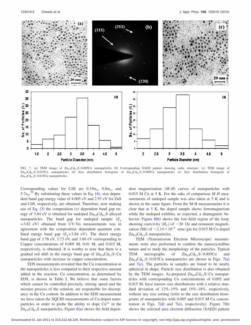
TEM �Transmission Electron Microscope� measure-ments were also performed to confirm the nanocrystallinenature and to study the morphology of the particles. TypicalTEM micrographs of Zn0.9Cd0.1S :0.005Cu andZn0.9Cd0.1S :0.015Cu nanoparticles are shown in Figs. 7�a�and 7�c�. The particles in samples are found to be nearlyspherical in shape. Particle size distribution is also obtainedby the TEM images. As-prepared Zn0.9Cd0.1S :Cu nanopar-ticles with corresponding Cu concentrations of 0.005 and0.015 M, have narrow size distributions with a relative stan-dard deviation of 12%–15% and 15%–18%, respectively,without any size sorting �refer to the size distribution histo-grams of nanoparticles with 0.005 and 0.015 M Cu concen-tration in Figs. 7�d� and 7�e�, respectively�. Figure 7�b�shows the selected area electron diffraction �SAED� pattern
FIG. 7. �a� TEM image of Zn0.9Cd0.1S :0.005Cu nanoparticles �b� Corresponding SAED pattern showing cubic structure. �c� TEM image ofZn0.9Cd0.1S :0.015Cu nanoparticles �d� Size distribution histogram of Zn0.9Cd0.1S :0.005Cu nanoparticles �e� Size distribution histogram ofZn0.9Cd0.1S :0.015Cu nanoparticles.
123519-5 Chawla et al. J. Appl. Phys. 108, 123519 �2010�
Downloaded 01 Jan 2011 to 210.212.58.229. Redistribution subject to AIP license or copyright; see http://jap.aip.org/about/rights_and_permissions
of Zn0.9Cd0.1S nanoparticles with characteristic of a cubicphase. In Fig. 7�b� the first ring indicates a periodical struc-ture with length of 3.1 Å, which is coincident with the stan-dard cubic Zn0.9Cd0.1S interplanar distance of 3.126 Å in the�111� direction, and is essentially the same as that obtainedby Vegard’s law.22 We also believe that there is no signatureof CuS or other impurity phases in our samples. XRD doesnot show any detectable signal of Cu or CuS, which meansthat the content of CuS or Cu in the samples is at most lessthan 5% �5% is the detection limit of XRD�. TEM diffractionpattern also support our argument as, we did not find anyother diffraction rings in our TEM diffraction pattern thatcannot be indexed by sphalerite structure. Also the undopednanoparticles show the diamagnetic behavior and the Cudoped Zn0.9Cd0.1S nanoparticle shows the ferromagnetic be-havior at temperature down to 5 K. This eliminates the pos-sibility of the existence of CuS or other impurity phases inthe samples.
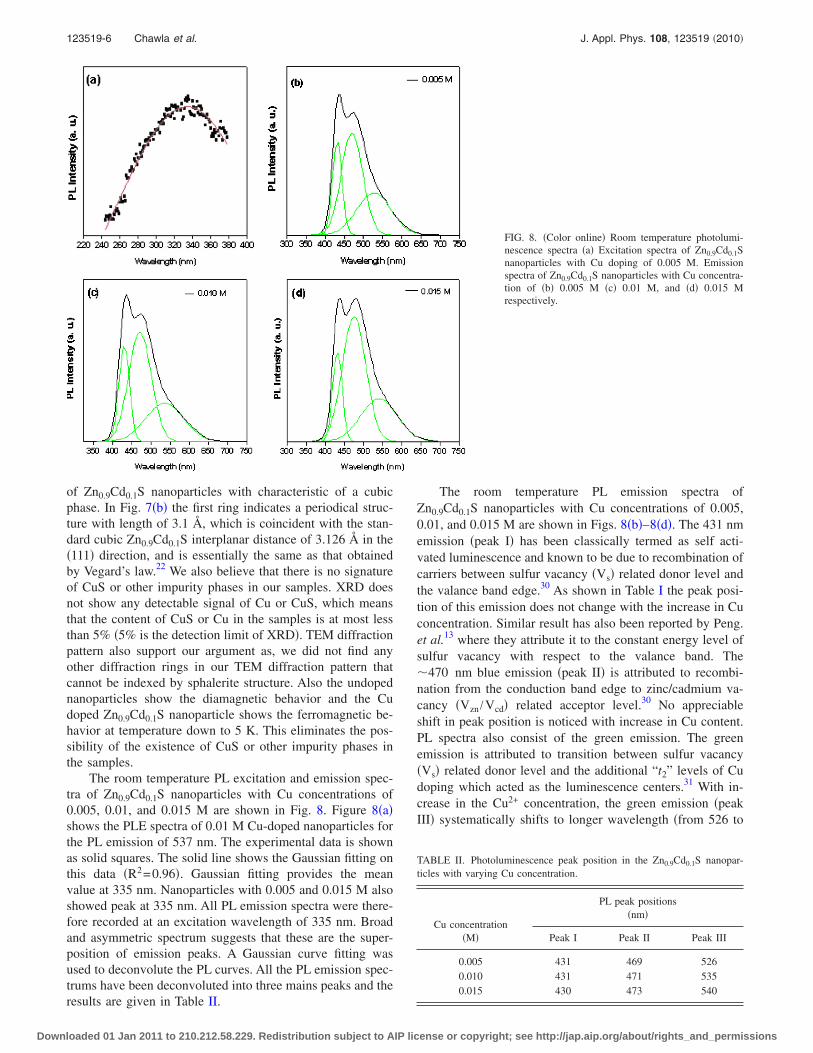
The room temperature PL excitation and emission spec-tra of Zn0.9Cd0.1S nanoparticles with Cu concentrations of0.005, 0.01, and 0.015 M are shown in Fig. 8. Figure 8�a�shows the PLE spectra of 0.01 M Cu-doped nanoparticles forthe PL emission of 537 nm. The experimental data is shownas solid squares. The solid line shows the Gaussian fitting onthis data �R2=0.96�. Gaussian fitting provides the meanvalue at 335 nm. Nanoparticles with 0.005 and 0.015 M alsoshowed peak at 335 nm. All PL emission spectra were there-fore recorded at an excitation wavelength of 335 nm. Broadand asymmetric spectrum suggests that these are the super-position of emission peaks. A Gaussian curve fitting wasused to deconvolute the PL curves. All the PL emission spec-trums have been deconvoluted into three mains peaks and theresults are given in Table II.
The room temperature PL emission spectra ofZn0.9Cd0.1S nanoparticles with Cu concentrations of 0.005,0.01, and 0.015 M are shown in Figs. 8�b�–8�d�. The 431 nmemission �peak I� has been classically termed as self acti-vated luminescence and known to be due to recombination ofcarriers between sulfur vacancy �Vs� related donor level andthe valance band edge.30 As shown in Table I the peak posi-tion of this emission does not change with the increase in Cuconcentration. Similar result has also been reported by Peng.et al.13 where they attribute it to the constant energy level ofsulfur vacancy with respect to the valance band. The�470 nm blue emission �peak II� is attributed to recombi-nation from the conduction band edge to zinc/cadmium va-cancy �Vzn /Vcd� related acceptor level.30 No appreciableshift in peak position is noticed with increase in Cu content.PL spectra also consist of the green emission. The greenemission is attributed to transition between sulfur vacancy�Vs� related donor level and the additional “t2” levels of Cudoping which acted as the luminescence centers.31 With in-crease in the Cu2+ concentration, the green emission �peakIII� systematically shifts to longer wavelength �from 526 to
FIG. 8. �Color online� Room temperature photolumi-nescence spectra �a� Excitation spectra of Zn0.9Cd0.1Snanoparticles with Cu doping of 0.005 M. Emissionspectra of Zn0.9Cd0.1S nanoparticles with Cu concentra-tion of �b� 0.005 M �c� 0.01 M, and �d� 0.015 Mrespectively.
TABLE II. Photoluminescence peak position in the Zn0.9Cd0.1S nanopar-ticles with varying Cu concentration.
Cu concentration�M�
PL peak positions�nm�
Peak I Peak II Peak III
0.005 431 469 5260.010 431 471 5350.015 430 473 540
123519-6 Chawla et al. J. Appl. Phys. 108, 123519 �2010�
Downloaded 01 Jan 2011 to 210.212.58.229. Redistribution subject to AIP license or copyright; see http://jap.aip.org/about/rights_and_permissions
540 nm�. This shift in green emission is due to increasedincorporation of Cu ions into Zn0.9Cd0.1S nanoparticles.
IV. CONCLUSIONS
The low temperature coprecipitation technique results inthe successful synthesis of cubic structured Cu-dopedZn1−xCdxS nanoparticles with controllable compositions andvery small sizes of around 3.5 nm. With increase in the Cdcontent, keeping Cu fixed at 0.005 M, absorption spectrared-shifts systematically, indicating the formation of the al-loyed nanoparticles. A decrease in band gap with increase incopper concentration in Zn0.9Cd0.1S is also observed. TEMdiffraction pattern confirms X-ray diffraction predictionsabout size and crystallinity of copper doped Zn0.9Cd0.1Snanoparticles. The magnetic measurement shows that the Cudoped Zn0.9Cd0.1S nanoparticles are ferromagnetic in naturewith coercivity �HC� of �20 Oe and remanent magnetiza-tion �Mr� of �2.14�10−5 emu /gm for 0.015 M Cu dopedZn0.9Cd0.1S nanoparticles. No signature of CuS or other im-purity phases are found in our samples. With increase in theCu2+ concentration, the green emission peak, attributed to therecombination between the shallow donor level �sulfur va-cancy� and the t2 level of Cu2+, systematically shifts from526 to 540 nm. This method can be used to synthesize smallsized doped and undoped ZnCdS nanoparticles with tunableoptical properties by varying either the constituents of hostor the concentration of dopant.
ACKNOWLEDGMENTS
We are grateful to Dr. A. C. Pandey, Director, Nanopho-spher Application Centre, Allahabad for providing the pho-toluminescence facility.
1S. J. Pearton, D. P. Norton, K. Ip, Y. W. Heo, and T. Steiner, J. Vac. Sci.Technol. 22, 932 �2004�.
2A. H. MacDonald, P. Shiffer, and N. Samarth, Nature Mater. 4, 195�2005�.
3H. Ohno, Science 281, 951 �1998�.4D. Jiang, L. Cao, G. Su, W. Liu, H. Qu, Y. Sun, and B. Dong, J. Mater. Sci.
44, 2792 �2009�.5X. Zhong and Y. Feng, Res. Chem. Intermed. 34, 287 �2008�.6R. Sethi, L. Kumar, and A. C. Pandey, J. Nanosci. Nanotechnol. 9, 5329�2009�.
7Y. M. Sung, Y. J. Lee, and K. S. Park, J. Am. Chem. Soc. 128, 9002�2006�.
8S. Singhal, A. K. Chawla, S. Nagar, H. O. Gupta, and R. Chandra, J.Nanopart. Res. 12, 1415 �2010�.
9A. A. Khosravi, M. Kundu, L. Jatwa, S. K. Deshpanee, U. A. Bhagwat, M.Sastri, and S. K. Kulkarni, Appl. Phys. Lett. 67, 2702 �1995�.
10B. Y. Geng, L. D. Zhang, G. Z. Wang, T. Xie, Y. G. Zhang, and G. W.Meng, Appl. Phys. Lett. 84, 2157 �2004�.
11S. J. Xu, S. J. Chua, B. Liu, L. M. Gan, C. H. Chew, and G. Q. Xu, Appl.Phys. Lett. 73, 478 �1998�.
12A. A. Bol, J. Ferwerda, J. A. Bergwerff, and A. Meijerink, J. Lumin. 99,325 �2002�.
13W. Q. Peng, G. W. Cong., S. C. Qu, and Z. G. Wang, Opt. Mater. 29, 313�2006�.
14A. Dutta, S. K. Panda, and S. Chaudhuri, J. Solid State Chem. 181, 2332�2008�.
15B. Geng, J. Ma, and F. Zhan, Mater. Chem. Phys. 113, 534 �2009�.16C. Unni, D. Philip, S. L. Smitha, K. M. Nissamudeen, and K. G. Gopchan-
dran, Spectrochim. Acta, Part A 72, 827 �2009�.17Y. T. Nien, P.W. Chen, and I. G. Chen, J. Alloys Compd. 462, 398 �2008�.18T. Y. Lui, J. A. Zapien, H. Tang, D. D. D. Ma, Y. K. Liu, C. S. Lee, S. T.
Lee, S. L. Shi, and S. J. Xu, Nanotechnology 17, 5935 �2006�.19J. U. Kim, Y. K. Kim, and H. Yang, J. Colloid Interface Sci. 59, 341
�2010�.20J. U. Kim, M. H. Lee, and H. Yang, Nanotechnology 19, 465605 �2008�.21B. D. Cullity and S. R. Stock, in Elements of X-Ray Diffraction, 3rd ed.,
edited by P. Hall �Prentice Hall, New Jersey, 2001�, p. 170.22J. Singh, Optoelectronics An Introduction to Materials and Devices
�McGraw-Hill, New York, 1996�.23L. Q. Yan, F. Macia, Z.-W. Jiang, J. Shen, L.-H. He, and F. W. Wang, J.
Phys.: Condens. Matter 20, 255203 �2008�.24A. P. Tsai, J. Non-Cryst. Solids 334–335, 317 �2004�.25D. Son, D. R. Jung, J. Kim, T. Moon, C. Kim, and B. Park, Appl. Phys.
Lett. 90, 101910 �2007�.26S. M. Sze, Physics of Semiconductor Devices �Wiley, New York, 1969�.27A. Goudarzi, G. M. Aval, R. Sahrai, and H. Ahmadpoor, Thin Solid Films
516, 4953 �2008�.28L. E. Brus, J. Chem. Phys. 80, 4403 �1984�.29H. Ohde, M. Ohde, F. Bailey, H. Kim, and C. M. Wai, Nano Lett. 2, 721
�2002�.30K. Jayanthi, S. Chawla, H. Chander, and D. Haranath, Cryst. Res. Technol.
42, 976 �2007�.31A. Dutta, S. Biswas, S. Kar, and S. Chaudhuri, J. Nanosci. Nanotechnol. 7,
3670 �2007�.
123519-7 Chawla et al. J. Appl. Phys. 108, 123519 �2010�
Downloaded 01 Jan 2011 to 210.212.58.229. Redistribution subject to AIP license or copyright; see http://jap.aip.org/about/rights_and_permissions