Band gap narrowing and fluorescence properties of nickel doped SnO 2 nanoparticles
6
Band gap narrowing and fluorescence properties of nickel doped SnO 2 nanoparticles Arham S. Ahmed a , Shafeeq M. Muhamed a , M.L. Singla b , Sartaj Tabassum c , Alim H. Naqvi a , Ameer Azam a,n a Centre of Excellence in Materials Science (Nanomaterials), Department of Applied Physics, Z. H. College of Engineering & Technology, Aligarh Muslim University, Aligarh-202002, India b Central Scientific Instruments Organization (CSIO), Council of Scientific & Industrial Research (CSIR), Materials Research and Bio-Nanotechnology Division, ector 30/C, Chandigarh-160030, India c Department of Chemistry, Aligarh Muslim University, Aligarh-202002, India article info Article history: Received 6 March 2010 Received in revised form 18 June 2010 Accepted 19 July 2010 Available online 18 August 2010 Keywords: Tin oxide nanoparticles Sol–gel XRD Band gap Fluorescence abstract Nickel-doped tin oxide nanoparticles (sub-5 nm size) with intense fluorescence emission behavior have been synthesized by sol–gel route. The structural and compositional analysis has been carried out by using XRD, TEM, FESEM and EDAX. The optical absorbance spectra indicate a band gap narrowing effect and it was found to increase with the increase in nickel concentration. The band gap narrowing at low dopant concentration ( o5%) can be assigned to SnO 2 SnO 2 x alloying effect and for higher doping it may be due to the formation of defect sub-bands below the conduction band. & 2010 Elsevier B.V. All rights reserved. 1. Introduction The wide variety of electronic and chemical properties of metal oxides makes them exciting materials for basic research and technological applications alike. Metal oxides span a wide range of electrical and optical properties from wide band gap insulators and lasers to metallic, superconducting and field emitting materials. Enormous efforts are being directed towards the development of nanometer sized metal oxides in studies related to their fundamental mechanisms such as size effect, quantum effect and towards the applications of these materials. Particle sizes in the nanoregime and specific crystal morphologies are expected to enhance the performance and allow the fine tuning of the properties of these materials. The optical properties of semiconducting nanoparticles have recently been a subject of great interest. Tin oxide (SnO 2 ) is a versatile wide band gap (3.6 eV at 300 K) n-type semiconducting oxide with a wide variety of applications. Because of its electrical and optical properties (transparent for visible light and reflective for IR) [1] allied to good chemical and mechanical stability [2], it is commonly used in many applications such as oxidation catalysis [3], gas sensing [4–6], transparent conducting oxides [7,8] and optoelectronic devices [9,10]. The properties of SnO 2 nanostruc- tures can be enhanced by several ways like impurity doping [11], coating with surfactants [12] and annealing [13]. One approach to produce strongly luminescent nanoparticles is to introduce small quantities of dopants. Hitherto, SnO 2 nanoparticles have been successfully doped with transition metal ions (Fe, Co, Mn and Cu) [11,14,15] and rare earth ions (Tb 3+ , Eu 3+ and Ce 3+ ) [9,15–17]. Many results have shown that several dopants (Co, Fe and Cu) can lead to an increase of surface area of SnO 2 by reducing the grain size and crystallanity [18–20]. Thus the final properties of impurity doped SnO 2 nanoparticles are related to both composi- tion and processing method. A number of methods such as co- precipitation [21], sol–gel [22–24], chemical vapour deposition [25,26], VLS method [27], laser ablation [28] and thermal redox process [29] have been developed for the preparation of SnO 2 nanoparticles. Among these methods, sol–gel is most effective due to its capability in controlling the structural and surface properties of nanoparticles. In this method, sol, gel or precipitate can be obtained depending on the chemical conditions. Generally, hydrolysis and condensation are fast and need to be inhibited to avoid precipitation and allow sol or gel formation. It has been reported that under appropriate conditions, solution to sol and then to gel formation can take place spontaneously in an aqua-alcoholic medium without introducing any precipitating agent [30]. We have adopted here a procedure in Contents lists available at ScienceDirect journal homepage: www.elsevier.com/locate/jlumin Journal of Luminescence 0022-2313/$ - see front matter & 2010 Elsevier B.V. All rights reserved. doi:10.1016/j.jlumin.2010.07.017 n Corresponding author. Tel.: + 91 9319788742; fax: + 91 5712700042. E-mail addresses: [email protected], [email protected] (A. Azam). Journal of Luminescence 131 (2011) 1–6
-
Upload
cas-historydeptt-amu -
Category
Documents
-
view
0 -
download
0
Transcript of Band gap narrowing and fluorescence properties of nickel doped SnO 2 nanoparticles

Journal of Luminescence 131 (2011) 1–6
Contents lists available at ScienceDirect
Journal of Luminescence
0022-23
doi:10.1
n Corr
E-m
(A. Azam
journal homepage: www.elsevier.com/locate/jlumin
Band gap narrowing and fluorescence properties of nickel dopedSnO2 nanoparticles
Arham S. Ahmed a, Shafeeq M. Muhameda, M.L. Singla b, Sartaj Tabassum c,Alim H. Naqvi a, Ameer Azam a,n
a Centre of Excellence in Materials Science (Nanomaterials), Department of Applied Physics, Z. H. College of Engineering & Technology, Aligarh Muslim University,
Aligarh-202002, Indiab Central Scientific Instruments Organization (CSIO), Council of Scientific & Industrial Research (CSIR), Materials Research and Bio-Nanotechnology Division,
ector � 30/C, Chandigarh-160030, Indiac Department of Chemistry, Aligarh Muslim University, Aligarh-202002, India
a r t i c l e i n f o
Article history:
Received 6 March 2010
Received in revised form
18 June 2010
Accepted 19 July 2010Available online 18 August 2010
Keywords:
Tin oxide nanoparticles
Sol–gel
XRD
Band gap
Fluorescence
13/$ - see front matter & 2010 Elsevier B.V. A
016/j.jlumin.2010.07.017
esponding author. Tel.: +91 9319788742; fax
ail addresses: [email protected], amee
).
a b s t r a c t
Nickel-doped tin oxide nanoparticles (sub-5 nm size) with intense fluorescence emission behavior have
been synthesized by sol–gel route. The structural and compositional analysis has been carried out by
using XRD, TEM, FESEM and EDAX. The optical absorbance spectra indicate a band gap narrowing effect
and it was found to increase with the increase in nickel concentration. The band gap narrowing at low
dopant concentration (o5%) can be assigned to SnO2�SnO2�x alloying effect and for higher doping it
may be due to the formation of defect sub-bands below the conduction band.
& 2010 Elsevier B.V. All rights reserved.
1. Introduction
The wide variety of electronic and chemical properties of metaloxides makes them exciting materials for basic research andtechnological applications alike. Metal oxides span a wide rangeof electrical and optical properties from wide band gap insulatorsand lasers to metallic, superconducting and field emittingmaterials. Enormous efforts are being directed towards thedevelopment of nanometer sized metal oxides in studies relatedto their fundamental mechanisms such as size effect, quantumeffect and towards the applications of these materials. Particlesizes in the nanoregime and specific crystal morphologies areexpected to enhance the performance and allow the fine tuning ofthe properties of these materials.
The optical properties of semiconducting nanoparticles haverecently been a subject of great interest. Tin oxide (SnO2) is aversatile wide band gap (3.6 eV at 300 K) n-type semiconductingoxide with a wide variety of applications. Because of its electricaland optical properties (transparent for visible light and reflectivefor IR) [1] allied to good chemical and mechanical stability [2], it iscommonly used in many applications such as oxidation catalysis
ll rights reserved.
: +91 5712700042.
[3], gas sensing [4–6], transparent conducting oxides [7,8] andoptoelectronic devices [9,10]. The properties of SnO2 nanostruc-tures can be enhanced by several ways like impurity doping [11],coating with surfactants [12] and annealing [13]. One approach toproduce strongly luminescent nanoparticles is to introduce smallquantities of dopants. Hitherto, SnO2 nanoparticles have beensuccessfully doped with transition metal ions (Fe, Co, Mn and Cu)[11,14,15] and rare earth ions (Tb3 +, Eu3 + and Ce3 +) [9,15–17].Many results have shown that several dopants (Co, Fe and Cu) canlead to an increase of surface area of SnO2 by reducing the grainsize and crystallanity [18–20]. Thus the final properties ofimpurity doped SnO2 nanoparticles are related to both composi-tion and processing method. A number of methods such as co-precipitation [21], sol–gel [22–24], chemical vapour deposition[25,26], VLS method [27], laser ablation [28] and thermal redoxprocess [29] have been developed for the preparation of SnO2
nanoparticles. Among these methods, sol–gel is most effectivedue to its capability in controlling the structural and surfaceproperties of nanoparticles. In this method, sol, gel or precipitatecan be obtained depending on the chemical conditions. Generally,hydrolysis and condensation are fast and need to be inhibited toavoid precipitation and allow sol or gel formation.
It has been reported that under appropriate conditions,solution to sol and then to gel formation can take placespontaneously in an aqua-alcoholic medium without introducingany precipitating agent [30]. We have adopted here a procedure in

A.S. Ahmed et al. / Journal of Luminescence 131 (2011) 1–62
this respect. Ni-doped SnO2 nanoparticles having sub-5 nm sizehave been successfully synthesized by sol–gel method in a water–ethylene glycol medium. The Ni doping in SnO2 resulted indecreasing the particle size and improving the luminescent emissionof the SnO2 nanoparticles. It is interesting to see that the band gapdecreases with decrease in the particle size and crystallanity.
Fig. 1. XRD spectra of pure and nickel doped SnO2 nanoparticles.
Table 1Variation of particle size, lattice parameter and band gap with dopant concentration.
Dopant
concentration
(%)
Crystallite
size (nm)
Lattice
parameter a (A)
Lattice
parameter c (A)
Band
gap (eV)
0 5.0 4.803 3.199 3.90
1 4.4 4.802 3.195 3.83
3 3.8 4.802 3.194 3.81
5 3.0 4.789 3.189 3.85
7 2.7 4.787 3.187 3.35
9 2.0 4.784 3.185 3.31
2. Experimental
2.1. Synthesis
SnCl4 �5H2O (Otto Kemi 98%) and NiCl2 �2H2O (Qualigens 98%)have been used as starting materials for the synthesis ofSn(1�x)NixO2 series. In a typical synthesis procedure, citric acid(Thomas Baker 99.5%) was added to 50 ml of distilled water withmagnetic stirring, until pH becomes 1.5. Now the requiredamounts of SnCl4 �5H2O and NiCl2 �2H2O with (x¼0, 0.01, 0.03,0.05, 0.07 and 0.09) were added and dissolved. 10 ml of ethyleneglycol was then added to the above solution and stirred for20 min. Now, sufficient amount of aqueous ammonia (15 mol/L)was added drop wise to the above solution under magneticstirring. The resulting solution was stirred for 30 min. Finally alight greenish gel was obtained, which was washed with waterand alcohol several times. Now, the gel was dried at 120 1C for15 h. The dried gel powder was further calcined at 350 1C for 2 hresulting the formation of Ni-doped SnO2 nanoparticles.
2.2. Characterization
Crystallanity, structure and particle size of Ni-doped SnO2
nanoparticles were determined by X-ray diffraction (XRD) usingRigaku-Miniflex X-ray diffractometer with CuKa radiations(l¼0.15406 nm) in 2y range from 201 to 801. Morphological analysiswas carried out on a FEI FE-SEM. The compositional analysis wascarried out using EDAX. The samples were coated with a thin layer ofgold to prevent charging of the samples. TEM analysis was carried outusing 200 kV JEOL transmission electron microscope. Optical absor-bance spectra of the samples were obtained using Perkin-ElmerUV–visible spectrophotometer. Fluorescent emission spectra wererecorded on a Varian Fluorescence spectrophotometer (Carry Eclipse).
3. Results and discussions
3.1. Structural properties
During synthesis, the pH value of the reaction medium playsan important role in the gel formation. At a particular pH, whenSnCl4 is hydrolyzed with ammonia solution, tin hydroxide isformed immediately as follows:
SnCl4 �5H2O+4NH4OH+H2O-Sn(OH)4+4NH4Cl+6H2O
Tin hydroxide thus formed is converted into SnO2 on annealingthe sample at 350 1C. The typical XRD patterns of the pure and Ni-doped SnO2 samples annealed at 350 1C are shown in Fig. 1. Thepeak positions of each sample exhibit the rutile type tetragonalstructure of SnO2, which were confirmed from the ICDD card No.77-0452. Further, no other impurity peak was observed in theXRD pattern showing the single phase sample formation. Thecrystalline size of all the samples were calculated using Scherrerformula [31], D¼ 0:9l=bcosy, where l is the wavelength of X-rayradiation, b is the full width at half maximum (FWHM) of thepeaks at the diffracting angle y. The calculated particle sizes ofeach sample are given in Table 1. It can be observed from Table 1
that the crystalline size of SnO2 decreased from 5 to 2 nm whenNi2 + content increased from 0% to 9% (see Fig. 2). Data revealedthat the presence of Ni2 + ions in SnO2 prevented the growth ofcrystal grains. The variations in the lattice parameter have alsobeen studied for different doping concentrations and presented inFig. 2. The ionic radius of Ni2 + is 69 pm whereas that of Sn4 + is71 pm. The Ni ions substitute the Sn4 + ions in the crystal due tocomparable ionic radius. However, the decrease in the latticeparameter may be due to the smaller ionic radius of Ni ions.
The XRD spectra have also been used to study the crystallanityof the samples. The doping of nickel in SnO2 not only lowers theparticle size but also degrades the crystallanity of the nanopar-ticles. Similar results have been reported earlier [32–34]. As the Nicontent increases, the intensity of XRD peaks decreases andFWHM increases (Fig. 1), which is due to the degradation ofcrystallanity. This means that even though the Ni ions occupy theregular lattice site of Sn4 +, it produces crystal defects around thedopants and the charge imbalance arising from this defectchanges the stoichiometry of the materials.
In order to investigate the dependence of crystallanity of thesamples on annealing temperature, sample with x¼0.05 wasannealed at different temperatures (450, 550 and 650 1C) for 2 h.The XRD patterns are shown in Fig. 3. Fig. 3 indicates that thecrystallanity of the sample increases while the FWHM decreaseswith the increase in annealing temperature. Crystallite size andlattice parameters were found to increase with the increase inannealing temperature as shown in Table 2. Furthermore, it hasbeen observed that there is no change in peak positions of XRDspectra, which indicate that the rutile structure remains the sameon annealing the sample at different temperatures.

A.S. Ahmed et al. / Journal of Luminescence 131 (2011) 1–6 3
Fig. 4 shows the typical morphology and composition of pure(Fig. 4a) and 5% Ni doped (Fig. 4b) SnO2 nanoparticles. The figureshows the presence of large spherical aggregates of smallerindividual nanoparticles and the presence of Ni is confirmed fromthe selective area EDAX analysis (Fig. 4). It can be verified fromthe results of XRD and EDAX that the Ni is successfully doped inthe SnO2 nanocrystals.
Fig. 5(a) and (b) shows TEM images taken for pure and 5%Ni-doped SnO2 nanoparticles, respectively. Powder samples weredispersed in ethanol and sonicated in an ultrasonic bath for15 min for TEM analysis. It is observed from Fig. 5 that SnO2
grains have a spherical morphology with an average diameter of15 nm for pure SnO2 and 9 nm for 5% Ni-doped SnO2, confirmingthe reduction in particle size as a result of Ni doping in SnO2.Particle size obtained from TEM analysis is slightly higher thanthe crystallite size calculated from XRD spectra.
3.2. Optical properties
Absorption and fluorescence spectroscopies are powerful non-destructive techniques to explore the optical properties of
Fig. 2. Variation of particle size and lattice parameter with nickel concentration.
Fig. 3. XRD spectra of Sn0.95Ni0.05
semiconducting nanoparticles. The optical absorption spectra ofpure and Ni doped SnO2 nanoparticles are shown in Fig. 6. Theabsorbance is expected to depend on several factors, such as bandgap, oxygen deficiency surface roughness and impurity centers.Absorbance spectra shows an ultraviolet cut-off around250–290 nm, which can be attributed to the photo-excitation ofelectrons from valence band to conduction band. The absorptionedge of different samples varies as the concentration of Ni in theSnO2 nanoparticles varies. In order to calculate the direct bandgap we used the Tauc relation
ahv¼ Aðhv�EgÞn
where a is the absorption coefficient, A is a constant. n¼1/2 fordirect band gap semiconductor. An extrapolation of the linearregion of a plot of (ahn)2 vs hn gives the value of the optical bandgap Eg. The measured band gap was found to be 3.9 eV forundoped SnO2 nanoparticles, which is higher than the reportedvalue of the bulk SnO2, i.e. 3.6 eV [11]. This can be attributed tothe quantum confinement effect of the nanoparticles [35]. Ondoping with nickel, the band gap energy decreases (Table 1), eventhough the particle size decreases. This is in contrast to thenormal phenomenon of quantum confinement. Chun-Ming et al.[36] have already reported band gap narrowing effect for dopedSnO2 nanoparticles. However there is no clear understandingof this phenomenon. A direct–indirect transition have beenproposed by Rakhshani et al. [37] In order to explain the bandgap narrowing effect, many groups have suggested that alloyingeffect of parent compound with some impurity phases may beresponsible for the band gap narrowing [36,38,39]. On one hand,the alloying effect from SnO2–NiO can be neglected because theband gap decreases below the band gap energy of NiO (3.54 eV)[40]. On the other hand no phase of NiO has been detected from
Table 2Variation of crystallite size and lattice parameters of Sn0.95Ni0.05O2 at different
temperatures.
Temperature
(1C)
Crystallite
size (nm)
Lattice
parameter a (A)
Lattice parameter
c (A)
350 3 4.789 3.189
450 5 4.790 3.191
550 9 4.792 3.192
650 10 4.793 3.194
O2 at different temperatures.

Fig. 4. SEM and EDAX images of (a) 0% (b) 5% Ni doped SnO2 nanoparticles.
Fig. 5. TEM images of (a) pure SnO2 (b) 5% Ni doped SnO2.
A.S. Ahmed et al. / Journal of Luminescence 131 (2011) 1–64
XRD measurements (Fig. 1). So the other possibility is theformation of SnO2�x phases in Ni2 + doped SnO2 than in pureSnO2. Chun-Ming et al. [36] have already reported the formationof SnO2�x phases in the sample. So we think that for the samplescontaining up to 5% Ni concentration, SnO2–SnO2�x alloying effectmay be responsible for the band gap narrowing effect. For theSnO2 nanoparticles above 5% Ni concentration there is a hugedrop in the band gap. This may be due to the formation of sub-bands in between the band gap, and the conduction band andsub-bands are merging with the conduction band to form a
continuous band. The fluorescence spectra of the pure and Nidoped SnO2 nanoparticles, which have been discussed in the nextsection are also consistent with the above observations.
Fig. 7 contains the photo-induced fluorescence spectra of allsamples for an excitation wavelength of 275 nm. The curves showtwo emission peaks, one centered at 315 nm and the other around375 nm. The first peak can be attributed to the near band edgeemission (NBE) coming from the radiative recombination ofelectrons in the conduction band and holes in the valence band.The band emission around 375 nm is due to several surface
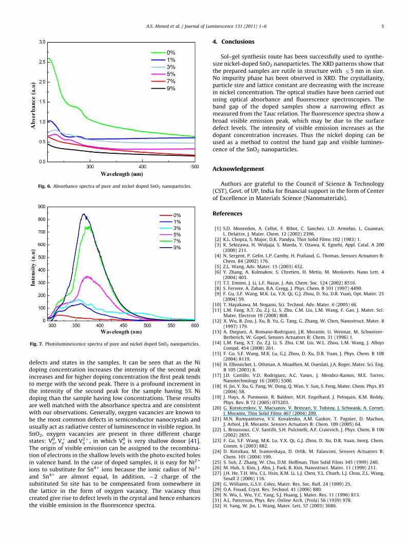
Fig. 6. Absorbance spectra of pure and nickel doped SnO2 nanoparticles.
Fig. 7. Photoluminescence spectra of pure and nickel doped SnO2 nanoparticles.
A.S. Ahmed et al. / Journal of Luminescence 131 (2011) 1–6 5
defects and states in the samples. It can be seen that as the Nidoping concentration increases the intensity of the second peakincreases and for higher doping concentration the first peak tendsto merge with the second peak. There is a profound increment inthe intensity of the second peak for the sample having 5% Nidoping than the sample having low concentrations. These resultsare well matched with the absorbance spectra and are consistentwith our observations. Generally, oxygen vacancies are known tobe the most common defects in semiconductor nanocrystals andusually act as radiative center of luminescence in visible region. InSnO2, oxygen vacancies are present in three different chargestates: V0
o, Vþo and V2þo , in which V0
o is very shallow donor [41].The origin of visible emission can be assigned to the recombina-tion of electrons in the shallow levels with the photo excited holesin valence band. In the case of doped samples, it is easy for Ni2 +
ions to substitute for Sn4 + ions because the ionic radius of Ni2 +
and Sn4 + are almost equal, In addition, �2 charge of thesubstituted Sn site has to be compensated from somewhere inthe lattice in the form of oxygen vacancy. The vacancy thuscreated give rise to defect levels in the crystal and hence enhancesthe visible emission in the fluorescence spectra.
4. Conclusions
Sol–gel synthesis route has been successfully used to synthe-size nickel-doped SnO2 nanoparticles. The XRD patterns show thatthe prepared samples are rutile in structure with r5 nm in size.No impurity phase has been observed in XRD. The crystallanity,particle size and lattice constant are decreasing with the increasein nickel concentration. The optical studies have been carried outusing optical absorbance and fluorescence spectroscopies. Theband gap of the doped samples show a narrowing effect asmeasured from the Tauc relation. The fluorescence spectra show abroad visible emission peak, which may be due to the surfacedefect levels. The intensity of visible emission increases as thedopant concentration increases. Thus the nickel doping can beused as a method to control the band gap and visible lumines-cence of the SnO2 nanoparticles.
Acknowledgement
Authors are grateful to the Council of Science & Technology(CST), Govt. of UP, India for financial support in the form of Centerof Excellence in Materials Science (Nanomaterials).
References
[1] S.D. Monredon, A. Cellot, F. Ribot, C. Sanchez, L.D. Armelao, L. Guanean,L. Delattre, J. Mater. Chem. 12 (2002) 2396.
[2] K.L. Chopra, S. Major, D.K. Pandya, Thin Solid Films 102 (1983) 1.[3] K. Sekizawa, H. Widjaja, S. Maeda, Y. Ozawa, K. Egnehi, Appl. Catal. A 200
(2000) 211.[4] N. Sergent, P. Gelin, L.P. Camby, H. Praliaud, G. Thomas, Sensors Actuators B:
Chem. 84 (2002) 176.[5] Z.L. Wang, Adv. Mater. 15 (2003) 432.[6] Y. Zhang, A. Kolmakov, S. Chretien, H. Metiu, M. Moskovits, Nano Lett. 4
(2004) 403.[7] T.T. Emons, J. Li, L.F. Nazar, J. Am. Chem. Soc. 124 (2002) 8516.[8] S. Ferrere, A. Zaban, B.A. Gregg, J. Phys. Chem. B 101 (1997) 4490.[9] F. Gu, S.F. Wang, M.K. Lu, Y.X. Qi, G.J. Zhou, D. Xu, D.R. Yuan, Opt. Mater. 25
(2004) 59.[10] T. Hayakawa, M. Nogami, Sci. Technol. Adv. Mater. 6 (2005) 66.[11] L.M. Fang, X.T. Zu, Z.J. Li, S. Zhu, C.M. Liu, L.M. Wang, F. Gao, J. Mater. Sci:
Mater. Electron 19 (2008) 868.[12] X. Wu, B. Zou, J. Xu, B. Yu, G. Tang, G. Zhang, W. Chen, Nanostruct. Mater. 8
(1997) 179.[13] A. Dieguez, A. Romano-Rodriguez, J.R. Morante, U. Weimar, M. Schweizer-
Berberich, W. Gopel, Sensors Actuators B: Chem. 31 (1996) 1.[14] L.M. Fang, X.T. Zu, Z.J. Li, S. Zhu, C.M. Liu, W.L. Zhou, L.M. Wang, J. Alloys
Compd. 454 (2008) 261.[15] F. Gu, S.F. Wang, M.K. Lu, G.J. Zhou, D. Xu, D.R. Yuan, J. Phys. Chem. B 108
(2004) 8119.[16] H. Elhouichet, L. Othman, A. Moadhen, M. Oueslati, J.A. Roger, Mater. Sci. Eng.
B 105 (2003) 8.[17] J.D. Castillo, V.D. Rodriguez, A.C. Yanes, J. Mendez-Ramos, M.E. Torres,
Nanotechnology 16 (2005) S300.[18] H. Jin, Y. Xu, G. Pang, W. Dong, Q. Wan, Y. Sun, S. Feng, Mater. Chem. Phys. 85
(2004) 58.[19] J. Hays, A. Punnoose, R. Baldner, M.H. Engelhard, J. Peloquin, K.M. Reddy,
Phys. Rev. B 72 (2005) 075203.[20] G. Korotcenkov, V. Macsanov, V. Brinzari, V. Tolstoy, J. Schwank, A. Cornet,
J. Morante, Thin Solid Films 467 (2004) 209.[21] M.N. Rumyantseva, V.V. Kovalenko, A.M. Gaskov, T. Pagnier, D. Machon,
J. Arbiol, J.R. Morante, Sensors Actuators B: Chem. 109 (2005) 64.[22] L. Broussous, C.V. Santilli, S.H. Pulcinelli, A.F. Craievich, J. Phys. Chem. B 106
(2002) 2855.[23] F. Gu, S.F. Wang, M.K. Lu, Y.X. Qi, G.J. Zhou, D. Xu, D.R. Yuan, Inorg. Chem.
Comm. 6 (2003) 882.[24] D. Kotsikau, M. Ivanovskaya, D. Orlik, M. Falasconi, Sensors Actuators B:
Chem. 101 (2004) 199.[25] S. Suh, Z. Zhang, W. Chu, D.M. Hoffman, Thin Solid Films 345 (1999) 240.[26] M. Huh, S. Kim, J. Ahn, J. Park, B. Kim, Nanostruct. Mater. 11 (1999) 211.[27] J.H. He, T.H. Wu, C.L. Hsin, K.M. Li, L.J. Chen, Y.L. Chueh, L.J. Chou, Z.L. Wang,
Small 2 (2006) 116.[28] G. Williams, G.S.V. Coles, Mater. Res. Soc. Bull. 24 (1999) 25.[29] O.A. Fouad, Cryst. Res. Technol. 41 (2006) 880.[30] N. Wu, L. Wu, Y.C. Yang, S.J. Huang, J. Mater. Res. 11 (1996) 813.[31] A.L. Patterson, Phys. Rev. Online Arch. (Prola) 56 (1939) 978.[32] H. Yang, W. Jin, L. Wang, Mater. Lett. 57 (2003) 3686.

A.S. Ahmed et al. / Journal of Luminescence 131 (2011) 1–66
[33] M. Hirano, K. Ota, H. Iwata, Chem. Mater. 16 (2004) 3725.[34] X. Fu, H. Zhang, S. Niu, Q. Xin, J. Solid State Chem. 178 (2005) 603.[35] T. Takagahara, K. Takeda, Phys. Rev. B 46 (1992) 15578.[36] L. Chun-Ming, F. Li-Mei, Z. Xiao-Tao, Z. Wei-Lie, Chin. Phys. 16 (2007) 95.[37] A.E. Rakhshani, Y. Makdisi, H.A. Ramazaniyan, J. Appl. Phys. 83 (1998) 1049.[38] Y.R. Park, K.J. Kim, J. Appl. Phys. 94 (2003) 6401.
[39] N. Barreau, J.C. Bernede, S. Marsillac, A. Mokrani, J. Cryst. Growth 235 (2002)439.
[40] B. Sasi, K.G. Gopchandran, P.K. Manoj, P. Koshy, P.R. Rao, V.K. Vaidyan,Vacuum 68 (2002) 149.
[41] K. Vanheusden, W.L. Warren, C.H. Seager, D.R. Tallant, J.A. Voigt, B.E. Gnade,J. Appl. Phys. 79 (1996) 7983.