Structural and Optical Properties of DNA Layers Covalently Attached to Diamond Surfaces
32
1 Structural and optical properties of DNA layers covalently attached to diamond surfaces Sylvia Wenmackers †,‡ , Simona D. Pop § , Katy Roodenko § , Veronique Vermeeren ||,‡ , Oliver A. Williams †,+ , Michael Daenen † , Olivier Douhéret †,+ , Jan D’Haen †,+ , An Hardy %,# , Marlies K. Van Bael %,+ , Karsten Hinrichs § , Christoph Cobet § , Martin vandeVen ||,‡ , Marcel Ameloot ||,‡ , Ken Haenen †,+ , Luc Michiels ||,‡ , Norbert Esser § , and Patrick Wagner *,†,‡ Hasselt University, Institute for Materials Research, Wetenschapspark 1, B-3590 Diepenbeek, Belgium, IMEC vzw, Division IMOMEC, Wetenschapspark 1, B-3590 Diepenbeek, Belgium, Hasselt University, Biomedical Research Institute, Agoralaan Building A, B-3590 Diepenbeek, Belgium, and Institute for Analytical Sciences, Department Berlin, Albert-Einstein-Straße 9, D-12489 Berlin, Germany. Label-free detection of DNA molecules on chemically vapor-deposited diamond surfaces is achieved with spectroscopic ellipsometry in the infrared and vacuum ultra-violet range. This non-destructive method has the potential to yield information on the average orientation of single as well as double stranded DNA molecules, without restricting the strand length to the persistence length. The orientational analysis based on electronic excitations in combination with information from layer thicknesses, provides a deeper understanding of biological layers on diamond. The π-π* transition dipole moments, corresponding to a transition at 4.74 eV, originate from the individual bases. They are in a plane perpendicular to the DNA backbone with an associated n-π* transition at 4.47 eV. For 8-36 bases of single and double stranded DNA covalently attached to ultra-nanocrystalline diamond, the ratio between in- and out-of-plane components in the best fit simulations to the ellipsometric spectra yields an average tilt angle of the DNA backbone with respect to the surface plane ranging from 45° to 52°.
Transcript of Structural and Optical Properties of DNA Layers Covalently Attached to Diamond Surfaces

1
Structural and optical properties of DNA layers
covalently attached to diamond surfaces
Sylvia Wenmackers†,‡, Simona D. Pop§, Katy Roodenko§, Veronique Vermeeren||,‡, Oliver A.
Williams†,+, Michael Daenen†, Olivier Douhéret†,+, Jan D’Haen†,+, An Hardy%,#, Marlies K. Van
Bael%,+, Karsten Hinrichs§, Christoph Cobet§, Martin vandeVen||,‡, Marcel Ameloot||,‡, Ken Haenen†,+,
Luc Michiels||,‡, Norbert Esser§, and Patrick Wagner*,†,‡
Hasselt University, Institute for Materials Research, Wetenschapspark 1, B-3590 Diepenbeek, Belgium,
IMEC vzw, Division IMOMEC, Wetenschapspark 1, B-3590 Diepenbeek, Belgium, Hasselt University,
Biomedical Research Institute, Agoralaan Building A, B-3590 Diepenbeek, Belgium, and Institute for
Analytical Sciences, Department Berlin, Albert-Einstein-Straße 9, D-12489 Berlin, Germany.
Label-free detection of DNA molecules on chemically vapor-deposited diamond surfaces is achieved
with spectroscopic ellipsometry in the infrared and vacuum ultra-violet range. This non-destructive
method has the potential to yield information on the average orientation of single as well as double
stranded DNA molecules, without restricting the strand length to the persistence length. The
orientational analysis based on electronic excitations in combination with information from layer
thicknesses, provides a deeper understanding of biological layers on diamond. The π-π* transition
dipole moments, corresponding to a transition at 4.74 eV, originate from the individual bases. They are
in a plane perpendicular to the DNA backbone with an associated n-π* transition at 4.47 eV. For 8-36
bases of single and double stranded DNA covalently attached to ultra-nanocrystalline diamond, the ratio
between in- and out-of-plane components in the best fit simulations to the ellipsometric spectra yields
an average tilt angle of the DNA backbone with respect to the surface plane ranging from 45° to 52°.

2
We comment on the physical meaning of the calculated tilt angles. Additional information is gathered
from atomic force microscopy, fluorescence imaging, and wetting experiments. The results reported
here are of value in understanding and optimizing the performance of the electronic read-out of a
diamond-based label-free DNA hybridization sensor.
* Corresponding author. E-mail: [email protected].
† Hasselt University, Material Physics - Institute for Materials Research.
‡ transnationale Universiteit Limburg, School for Life Sciences.
§ Institute for Analytical Sciences, Department Berlin.
|| Hasselt University, Biomedical Research Institute.
+ IMEC vzw, Division IMOMEC.
% Hasselt University, Inorganic and Physical Chemistry – Institute for Materials Research.
# XIOS Hogeschool Limburg, Department Industrial Sciences and Technology.

3
1. Introduction
A better understanding and characterization of layers of terminally attached deoxyribonucleic acid
(DNA) molecules on a surface, DNA brushes, is important for improving genetic assays, where single
stranded (ss) probe DNA is immobilized on a solid support and coupled (hybridized) to target ssDNA
molecules from solution.
For electrical sensing, the substrate for attachment of the DNA probes should preferably be a metal or
semiconductor. The material should be stable in solution and receptive for the covalent attachment of
probe DNA. DNA brushes have successfully been prepared and extensively studied on materials such as
silicon oxide1 and gold.2-8 In recent years, diamond obtained from chemical vapor deposition (CVD)
gained interest with regard to biosensor applications. This stable, highly biocompatible material, can be
applied in electrical sensing, thanks to its wide band gap and large electrochemical potential window.9,10
Diamond surfaces range from single crystalline to ultra-nanocrystalline films,11 and from undoped to
(heavily) boron doped. Its surface has been functionalized successfully with various bio-molecules:
DNA,12-15 as well as immunoglobulins G and M (IgG and IgM),16 and enzymes such as catalase,17
urease and glucose oxidase,18 as well as horse radish peroxidase.19 DNA sensors for in vitro use only
require a biocompatible top-layer, to which the probe DNA is anchored and where interaction with
target DNA samples takes place. Diamond-coated silicon wafers are a good starting material, as they are
easier to produce and cheaper than an all-diamond biosensor. Ultra-nanocrystalline diamond (UNCD®)
coated silicon was indeed found to be a very stable platform for DNA.12 In the current study, we will
therefore focus on DNA layers grafted on nanocrystalline (NCD) and UNCD coated silicon.
Important parameters for good sensor functioning (hybridization) are the density and the orientation
of the DNA molecules in the sensing layer. Molecular dynamics simulations of DNA molecules, based
on classical worm-like chain (WLC) theory and adaptations thereof,20,21 are in good agreement with
recent experimental findings, such as cyclization studies,12,22 bending force measurements based on
magnetic tweezers and single-molecule fluorescence microscopy,23 as well as AFM studies of DNA
layers lying flat on mica.24 However, it is not straightforward to predict, starting from these models for

4
the mechanical properties of DNA, the behavior of surface-bound DNA molecules. In DNA brushes, the
density of the layer will most probably influence the orientation of the molecules. Therefore, we will
first distinguish between ‘dilute’ and ‘dense’ DNA layers.
We will call the layer ‘dilute’ when the DNA spacing is comparable to or larger than the stretched-out
length of the molecules, which implies that they do not interact substantially. The orientation of DNA in
low density layers on gold substrates has been studied theoretically,25 as well as experimentally.26-29
One approach is to monitor the interfacial fluorescence quenching, which increases when the
fluorescence dye at the distal end of DNA is brought closer to a gold substrate, while the gold electrode
is biased to alternately positive and negative potentials.26 Also atomic force microscopy (AFM) and
scanning tunneling microscopy (STM) are applied to dilute,27-29 as well as ‘dense’ DNA layers on
gold.2,3 When the DNA is in a dense layer, the molecules do interact, and the conformation and
orientation of the molecules can become strongly affected by these interactions. These studies estimate
the average tilt angles from the plane of the surface for DNA molecules on gold to be in the range of
45° to 60°. In a cyclic voltammetry study, using a ferrocene label at the distal end of DNA on gold
electrodes, it was found that the DNA molecules can bend as well as rotate under applied electric
fields.5 The previously mentioned range for the average tilt angle of double stranded (ds) DNA
molecules could be narrowed to 55° to 60°. In recent literature, the process steps of covering diamond
with dense DNA layers have been validated using a variety of techniques, including X-ray
photoelectron spectroscopy (XPS),12,30,31 AFM,14,32-34 ultraviolet photoelectron spectroscopy (UPS),30
electrochemical impedance spectroscopy (EIS),35-37 enzyme linked immunosorbent assays (ELISA),31
amplification by polymerase chain reaction (PCR) followed by gel electrophoresis,13 and fluorescence
microscopy (FM).12-14,31 Of this list, only the tapping mode (or intermittent-contact mode) AFM
studies14,32-34 were specifically aimed at clarifying the orientation of DNA molecules in dense layers.
Based on the measurement of the DNA layer thickness, Rezek and Nebel report average tilt angles for
16 bp dsDNA on single crystalline diamond in the range of 30° to 37° with respect to the surface14,34.

5
This estimation applies only to the analysis of short dsDNA, since it assumes that the molecules in the
layer are straight.
In this work, the orientation of dense DNA molecules on CVD diamond is investigated. We use
spectroscopic ellipsometry (SE) – both in infrared (IR) and ultra-violet (UV) – as a complementary
technique to AFM. The SE approach allows the evaluation of layer thicknesses as well as average tilt
angles, with the advantage of being applicable to both short and long DNA, and for both ds and ssDNA.
SE is a useful characterization method for polymer brushes in general.38 The samples in the current
study consist of DNA end-grafted on NCD and UNCD surfaces. Functionalization is done by a two-step
protocol, involving the photo-attachment of fatty acids to form a linker layer, followed by the covalent
DNA attachment using a zero-length crosslinker, as reported in detail previously,13 and confirmed later
on.15,39 To check whether the DNA forms a homogeneous layer we apply FM, as well as AFM for
information on smaller scales. Based on the observation of vibrational bands, IR SE enables a direct,
label-free proof of the DNA attachment, together with an estimation of the layer thickness. This
technique has been used previously to determine the average tilt angle in guanine films on silicon.40
With UV SE, electronic excitations are monitored, the orientation can be deduced,41 and ss and dsDNA
can be distinguished, as was already observed for non-surface-bound DNA in the early sixties.42,43 DNA
molecules are particularly interesting to be studied with SE in the UV range, because they contain
transition dipole moments oriented along two well-defined directions: in the plane of the bases and,
perpendicular to this, along the backbone of the strands.44,45 SE has already been applied to study films
of single bases on silicon,40,45 but to our knowledge this is the first report on its application to study the
average tilt angle of integral DNA molecules on CVD diamond surfaces. Although the analysis of SE
measurements is more straightforward for atomically flat substrates, the roughness of NCD and
especially UNCD films is low and regular enough to correct for by introducing an additional layer in the
optical model, with intermediate optical properties.

6
2. Materials and Methods
Diamond preparation. After mechanical seeding of a Si(100) substrate with diamond powder, NCD
films thinner than 200 nm were deposited, using a plasma enhanced (PE) CVD reactor “ASTeX®
AX6550” from Seki Technotron Corp. (Tokyo, Japan) equipped with a 2.45 GHz microwave generator
set at 3000 W, and applying 485 sccm H2 (standard cubic centimeter per minute), 15 sccm CH4, 40 Torr
(= 5.3 kPa), 730°C for 80 min.11 Typically, the NCD thickness decreases radially from the centre of the
wafer, while UNCD shows a more homogeneous thickness throughout the wafer. Because thickness
variations cause the background signal in SE to differ from place to place, also a 2 µm thick film of
UNCD on a Si wafer, ‘AQUA 25’, deposited by Advanced Diamond Technologies (Romeoville, IL
USA), was purchased through GoodFellow (Cambridge, UK).
The NCD and UNCD wafers were divided into 1 cm² squares and cleaned for 30 minutes in an
oxidizing mixture of boiling sulfuric acid (H2SO4 98-100% pure, VWR International, Zaventem,
Belgium) and potassium nitrate (KNO3, ≥ 99%, Merck, Leuven, Belgium). This procedure was followed
by thoroughly washing in distilled, ultra-pure water (18.2 MΩ.cm, obtained by filtering distilled water
through an “Arium® 611 system”, Sartorius, Göttingen, Germany): the water was changed six times,
alternately heated and put in an ultrasonic cleaner (“Branson 1510”, Branson, Danbury, UK).
Afterwards, the samples were dried under a flow of nitrogen gas. The final H-termination was
performed in a plasma at 700°C during 1 minute at 3000 W, 35 Torr (= 4.7 kPa) with 1000 sccm H2.
Silicon preparation. For an ellipsometry reference experiment, three 1.5×1.5 cm2 pieces of n-type
Si(100) were H-terminated by the following three step treatment.46-49 Firstly the samples were dipped in
a mixture of H2SO4 (95%; Merck) and H2O2 (35%; Acros Organics) in a 4:1 volume ratio, secondly in a
mixture of H2O, H2O2 and NH3 (32%; Merck) in 5:1:1 volume ratios, and thirdly in 5% HF (VWR
International). Afterwards, the samples were rinsed in ultra-pure water and blown dry under nitrogen.
The successful H-termination was evidenced by measurement of a grazing angle attenuated total
reflection Fourier-transform IR (GATR-FTIR) spectrum (resolution 4 cm-1; GATR Harrick, FTIR
Bruker Vertex, Brussels, Belgium): peaks at 2137, 2114 and 2089 cm-1 were prominent, which are

7
attributed to the presence of SiH3, SiH2 and SiH respectively.49 The H-terminated Si samples were put
under the protective atmosphere of a nitrogen filled glovebox, after a short transportation time
(~minutes) in air.
Diamond and silicon functionalization. Part of the H-terminated NCD, UNCD and Si samples were
used for further functionalization. The NCD samples have been prepared exactly as described in
reference 13, while the UNCD sample have been treated with the optimized conditions of reference 39.
(Details on the functionalization can be found in the Supporting Information 1, Diamond
functionalization, Fig. S1 and Table S1.) 10-undecenoic acid (UA) (Merck) is reacted with the surface
during 20h under 254 nm UV illumination. This photo-reaction results in a carboxyl-terminated surface.
Subsequent covalent coupling of amino-modified dsDNA to the carboxyl-terminated surface was
carried out using the zero-length crosslinker 1-ethyl-3-[3-dimethylaminopropyl]-carbodiimide (EDC)
(Perbio Science, Erembodegem, Belgium). This was done in 2-[N-morpholino]-ethanesulphonic acid
(MES) buffer (Perbio Science). Here, different lengths of DNA were used, both ss of 8 or 36 b and ds of
250 bp, all with an amino-group at the 5’ side. Part of the samples covered with 36 b ssDNA probes
were allowed to hybridize to its perfect complement (29 b). The 250 bp dsDNA sample was denatured
in 0.1 M sodium hydroxide (NaOH; Merck) to obtain a layer of 250 b ssDNA. For an SE reference
experiment, a H-terminated sample was prepared with a multilayer of adsorbed DNA, formed by drying
of a droplet of 250 bp dsDNA in buffer solution on an NCD substrate. The name codes for the various
diamond samples can be found in Table 1. The UA functionalization of two of the Si(100) samples was
performed similar to the method optimized for diamond,39 but with the UV illumination time limited to
3 h to prevent the formation of a polymerized UA layer. One of the UA-terminated Si samples was then
functionalized with 250 bp dsDNA.

8
Table 1: Overview of NCD and UNCD samples.
Sample name Type of diamond Surface termination
“N1” NCD Oxidized
“N2” NCD H-terminated
“N3”* NCD UA-linker layer
“N4”* NCD Brush of 250 bp dsDNA
“N5” NCD Adsorbed layer of 250 bp dsDNA
“U1” UNCD Oxidized
“U2” UNCD H-terminated
“U3” UNCD UA-linker layer
“U4+” UNCD Brush of 8 b ssDNA
“U4-” UNCD UA-linker layer and 8 b ssDNA without EDC
“U5” UNCD UA-linker layer and 8 b ssDNA without EDC
“U6” UNCD Brush of 36 b ssDNA
“U7” UNCD Brush of 29 bp dsDNA
*: these samples have been treated as described in reference 13.
Characterization techniques. For a morphology study, atomic force microscopy (AFM) was
performed in tapping mode with a Veeco Multimode microscope (Veeco Instruments, Santa Barbara,
CA USA) equipped with the Nanoscope III controller extended with the Quadrex module (phase signal
imaging); high spatial resolution measurements (sub 10 nm) were ensured by the use of etched Si tips
attached at the extremity of a standard non-contact mode cantilever (Nanosensors, Neuchâtel,
Switzerland).
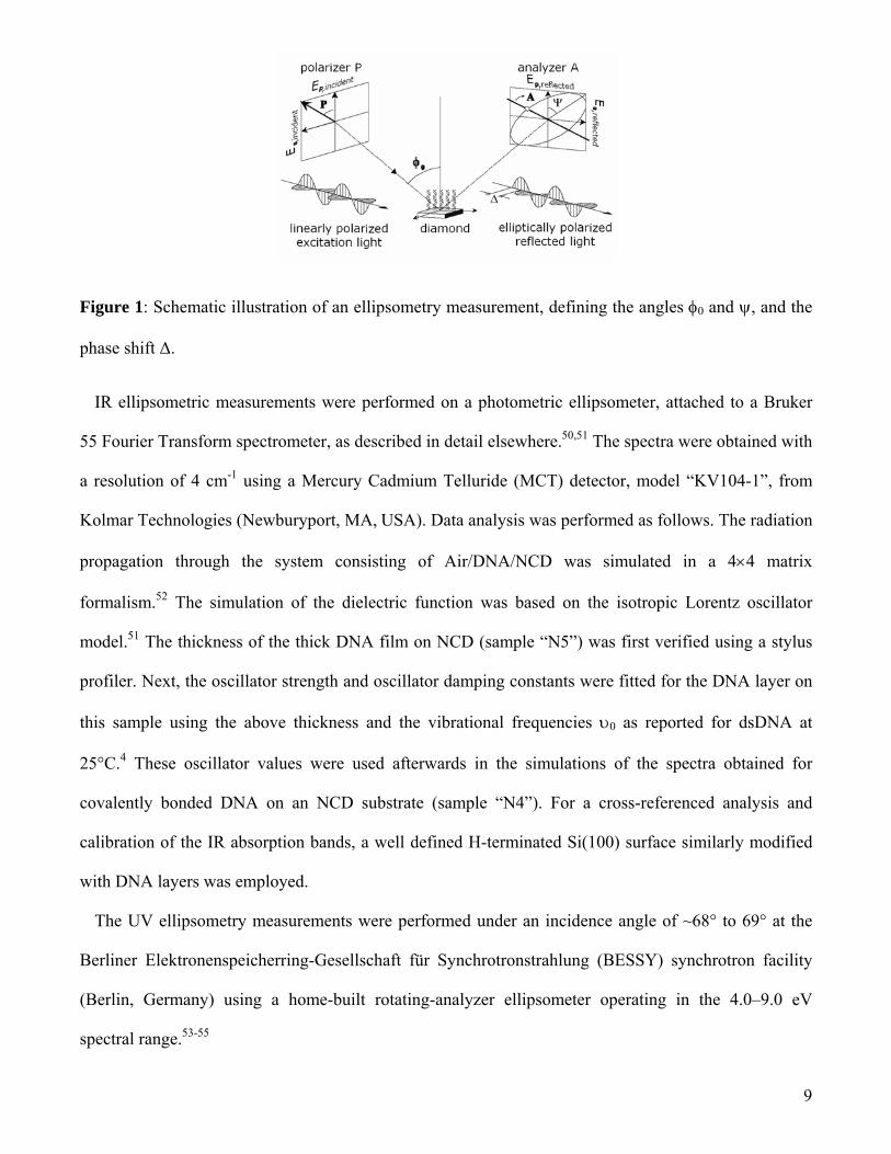
Spectroscopic ellipsometry (SE) analyzes the changes in the polarization state of radiation reflected
from a dry sample surface (Fig. 1). These changes can be described by the measured ellipsometric
parameters, tan(ψ) and Δ. The ellipsometric parameter tan(ψ) represents the amplitude ratio of the
complex reflection coefficients parallel (rs) and perpendicularly (rp) polarized with respect to the plane
of incidence (tan(ψ) = |rp/rs|), while Δ is the phase shift between them (Fig. 1).
9
Figure 1: Schematic illustration of an ellipsometry measurement, defining the angles φ0 and ψ, and the
phase shift Δ.
IR ellipsometric measurements were performed on a photometric ellipsometer, attached to a Bruker
55 Fourier Transform spectrometer, as described in detail elsewhere.50,51 The spectra were obtained with
a resolution of 4 cm-1 using a Mercury Cadmium Telluride (MCT) detector, model “KV104-1”, from
Kolmar Technologies (Newburyport, MA, USA). Data analysis was performed as follows. The radiation
propagation through the system consisting of Air/DNA/NCD was simulated in a 4×4 matrix
formalism.52 The simulation of the dielectric function was based on the isotropic Lorentz oscillator
model.51 The thickness of the thick DNA film on NCD (sample “N5”) was first verified using a stylus
profiler. Next, the oscillator strength and oscillator damping constants were fitted for the DNA layer on
this sample using the above thickness and the vibrational frequencies υ0 as reported for dsDNA at
25°C.4 These oscillator values were used afterwards in the simulations of the spectra obtained for
covalently bonded DNA on an NCD substrate (sample “N4”). For a cross-referenced analysis and
calibration of the IR absorption bands, a well defined H-terminated Si(100) surface similarly modified
with DNA layers was employed.
The UV ellipsometry measurements were performed under an incidence angle of ~68° to 69° at the
Berliner Elektronenspeicherring-Gesellschaft für Synchrotronstrahlung (BESSY) synchrotron facility
(Berlin, Germany) using a home-built rotating-analyzer ellipsometer operating in the 4.0–9.0 eV
spectral range.53-55

10
3. Results
Scanning electron microscopy (SEM) images of the H-terminated NCD and UNCD surfaces can be
found in Supporting Information 2 (Fig. S2 and S3). The functionalization steps have been validated
using wetting studies (Supporting Information 3, Table S3) and fluorescence microscopy of labelled
DNA (Supporting Information 4, Fig. S4-6), where the use of shadow masks during the photo-
attachment of the linker layer is shown to yield clear patterns in the DNA layers (Fig. S7).
3.1. Morphology and roughness of NCD and UNCD surfaces. To obtain quantitative information
on the roughness of the UNCD samples, tapping mode AFM experiments are performed on dry surfaces
under ambient conditions.
3.1.1. NCD and UNCD surfaces with H- or UA-layer. The root mean square (RMS) roughness of
the bare, H-terminated UNCD film (sample “U2”) in Fig. 2 (a) is ~17 nm as determined with AFM on
scales of (4 µm)² down to (1 µm)². The individual grains (sized between 3 to 50 nm) can be identified
best in the phase image; in the normal height image larger clusters of grains can be seen. After photo-
attachment of the UA linker molecule (sample “U3”), in Fig. 2 (b) the morphology and RMS roughness
values do not significantly change. This is to be expected, since the length of a UA molecule is small (2
nm) compared to the surface roughness of the underlying UNCD film. No additional structures are
found, indicating a homogeneous attachment of the UA layer to the surface, not limited to preferential
sites (e.g. grain boundaries).

11
Figure 2: 1 µm × 1 µm height and phase AFM images collected in tapping mode, in ambient conditions
on a) H-terminated UNCD (sample “U2”), and on b) 10-undecenoic acid terminated UNCD (sample
“U3”).
3.1.2. NCD and UNCD surfaces with DNA-layer. Since the film roughness may have an impact on
further ellipsometry results, we studied the change in morphology and RMS roughness of UNCD
surfaces upon DNA attachment, by AFM in tapping mode. Although AFM measurements on DNA
layers in buffer solutions are possible,32 here the samples have been dried and measured in ambient
conditions, because the ellipsometry measurements are (necessarily) performed on dry samples. The
results are presented in Fig. 3. Throughout the measurements, the structures of the underlying UNCD
stay dominant. To prevent denaturation, the samples with dsDNA are not rinsed in ultra-pure water, but
dried with nitrogen directly from PBS buffer solution (containing NaCl, Na3PO4, and K3PO4). This
causes some salt crystals, appearing as white spots in the height image (dark in the phase image) of Fig.
3 (c). In Fig. 3 (d) one such salt crystal is visible. However, the roughness is not significantly different
for surfaces with H-termination only, or covered with an UA linker layer or with a layer of short ssDNA
(8 b). For longer DNA (36 b), both in ss and ds form, the RMS roughness does decrease (Fig. 4). One
can conjecture that here the biological top layer fills the dips between grains and grain clusters of the
UNCD surface.

12
Figure 3: Height and phase AFM images in tapping mode, under ambient conditions on dry UNCD
samples with varied surface terminations: a) UNCD with ssDNA of 8 b (sample “U5”), b) UNCD with
ssDNA of 36 b (sample “U6”), and c) UNCD with dsDNA of 29 bp (on top of an A7-ss-tail) (sample
“U7”). d) More detailed scan of the square area indicated in part c).
Figure 4: Comparison of RMS values of dry UNCD surfaces with different surface terminations as
determined with tapping mode AFM on different scanning scales.
3.2. Label-free optical detection of DNA layers (in dry condition)

13
3.2.1. Average layer thickness of DNA layers on NCD. Ellipsometry in the IR range allows for a
direct, label-free proof of the DNA immobilization on an NCD substrate. Fig. 5 shows typical spectra of
DNA adsorbed or covalently attached to NCD and Si(100), in the region of the ‘amide I’ band, related
to vibrations of amino and carbonyl groups.4,56 All films show similar absorption properties, indicating
that the DNA attachment was successful. Fig. 5 (c) also shows IR SE spectra for the UA-terminated
Si(100) sample. The band around 1720 cm-1 is due to the carbonyl stretching vibrations of the
carboxylic acid.57 Upon DNA-attachment (Fig. 5 (d)), this band disappeared from the spectra of DNA
on Si(100) samples, while the CH2-related stretching vibrations of the hydrocarbon chains of the UA in
the range between 2830-2980 cm-1 57 remained unchanged. We did not observe similar bands on UA-
terminated NCD substrates, probably due to a lower signal-to-noise ratio. The simulation of the
measured results for DNA-terminated surfaces is shown in Fig. 5 by black solid lines. The simulated
spectra were achieved using the isotropic Lorentz oscillator model and radiation propagation in a three
layer Air/DNA/Substrate system, as described in detail in the "Materials and Methods" section. The
determined thickness for the adsorbed 250 bp dsDNA layer on NCD (sample “N5”) is d = 200 nm, and
the high-frequency refractive index is n∞ = 1.51. The oscillator parameters obtained from the
simulations of the thick film data are then used to determine the thickness of the covalently-attached
DNA layers on NCD (sample “N4”) and Si(100) surfaces. Under the assumption that these films are
isotropic, the calculations resulted in 40 nm thickness for 250 b ssDNA on NCD and 9 nm thickness for
250 bp dsDNA on Si(100) (with n∞ = 1.51). The thickness of DNA on Si(100) was cross-checked with
the ellipsometric measurements in the visible (VIS) spectral range. Estimated thickness accuracy is
within 20% from the obtained thickness values, taking into account the results obtained from different
methods and IR SE simulations on various samples. The high-frequency refractive index n∞=1.51 ± 0.03
as found by VIS ellipsometry and IR SE was in a good agreement with literature data.58,59
We would like to point out that the IR intensities reported in this work for layers of entire DNA
molecules are in general smaller than those obtained for films of single DNA bases (i.e. adenine,
thymine, guanine, and cytosine).45 This decrease in intensity and frequency shifts upon base pairing has

14
also been observed by other authors.57,60 However, additional studies are necessary in order to relate the
IR intensities of the single DNA bases to those of DNA molecules.
The thickness as found for 250 b ssDNA covalently attached on NCD is less than the stretched-out
length of the DNA, i.e. 150 nm. We give two possible explanations for this observation. First, the DNA
strands are longer than the persistence length, the length scale over which dsDNA maintains its tangent
orientation, i.e. ~2 nm,61,62 so they are almost certainly not fully stretched on the NCD surface. For
shorter DNA, there is a possibility of a tilt angle with respect to the diamond surface. Unfortunately, the
complexity of the bands in the ‘amide I’ region does not allow for the determination of such a tilt angle,
as was done in the case of pure guanine films using IR ellipsometry.40 Therefore, we have investigated
the band at 4.74 eV, with UV SE, as will be described now.
Figure 5: Referenced ellipsometric parameters tan(ψ) and Δ as obtained in IR SE measurements at 65°
incidence angle. a) Adsorbed 250 bp dsDNA on NCD (sample “N5”); b) covalently attached 250 b
ssDNA on NCD (sample “N4”); c) Si(100)-UA; d) Si(100)-UA-DNA. The grey dotted lines represent
measured data referenced to a bare, H-terminated substrate; the simulations are presented as a black,
solid line. Tan(ψ)S and ΔS refer to the H-terminated NCD substrate, whereas tan(ψ)F and ΔF refer to the
sample with organic functionalisation. In (b) the difference in background between the measured data

15
and the simulation are due to differences between the H-terminated NCD reference sample and the NCD
underlying the DNA film. In (d), the feature at about 1720 cm-1 arises from referencing to the UA-
terminated Si(100) shown in (c), related to the C=O carbonyl group of the linker. The evaluated layer
thicknesses are indicated on the plots. The high-frequency refractive index was n∞ = 1.51 in the
calculations. In all calculations, substrates were simulated using the measured substrate optical
constants, i.e. the refractive index n and the extinction coefficient k.
3.2.3. Average tilt angle of DNA molecules on NCD and UNCD. Besides IR SE, also ellipsometry
in the vacuum ultra-violet (VUV) spectral range was applied, which reveals specific information on the
electronic fingerprint of DNA molecules. The UV SE spectra of the thin, covalently attached DNA layer
attached to an NCD substrate (sample “N4”) are presented in Fig. 6 (a). The ellipsometric parameters
tan(ψ) and Δ have been calculated using a three layer model (as explained under "Materials and
Methods") assuming a DNA layer thickness of 40 nm and a high-frequency refractive index, n∞ = 1.51,
as determined by IR SE. The optical response of the ssDNA layer was described by a sum of Lorentz
functions. The obtained isotropic optical constants are displayed in Fig. 6 (b). The energy positions of
the employed Lorentz functions are indicated by arrows. The typical π-π* electronic transition
(representing an orbital change from bonding to anti-bonding) of the DNA molecule is observed at 4.74
eV (261 nm) in agreement with the values reported already in early literature.44 Although it is well
known that UV can damage DNA,63-65 the presence of this non-shifted π-π* electronic transition
suggests that UV dose is low enough during the UV SE measurement for the DNA layer to remain
intact. This absorption band is assigned to the π-π* electronic transitions of the single DNA bases.40,44
In the higher energy range the absorption structures are dominated by mixed π-π* and σ-σ* electronic
transitions which belong to both single bases and sugar phosphate groups.44

16
Figure 6: Covalently attached monolayer of 250 b ssDNA on dry NCD (sample “N4”). a) Measured and
calculated ellipsometric spectra tan(ψ) and Δ of this sample. b) Derived optical constants, refractive
index (n) and extinction coefficient (k). The assignment of the main electronic transitions of DNA
molecules is indicated by arrows.
The steep increase in the absorption above 7 eV is mainly due to σ-σ* transitions of the phosphate
groups.44 The lowest electronic transition at 4.47 eV (277 nm) assigned as an n-π* transition is a
fingerprint for the molecular orientation, but also discriminates between the ss and ds conformation of
DNA molecules.42,43 The molecular orientation can be deduced, knowing that the n-π* transition dipole
moment is directed along the DNA backbone, which is perpendicular to the π-π* transition dipole
moments of the individual bases, as is schematically depicted in Fig. 7. On sample “N4”, the optical
response of the 250 b ssDNA layer is isotropic, meaning that the DNA molecules are mostly randomly
distributed on the NCD substrate. This was to be expected, since ssDNA is a highly flexible polymer
with a persistence length of only ~2 nm,61,62 much shorter than its stretched-out length of 150 nm.

17
Figure 7: Schematic representation of the transitions at 4.47 and 4.74 eV in dsDNA.
Further UV SE experiments have been conducted for diamond surfaces terminated with a dense layer
of short covalently attached DNA molecules, where a preferential orientation is expected. We have
opted for DNA-functionalized UNCD rather than NCD, since the higher intrinsic roughness of NCD
and its radially varying thickness was occasionally found to interfere with the signal coming from the
DNA top layer. The dose of UV illumination during the UV SE experiments was low enough not to
degrade the DNA films. This has been checked by measuring the same spot of the same sample twice,
which resulted in exactly the same spectrum.
Fig. 8 shows the measured ellipsometric spectra of an H-terminated UNCD substrate (sample “U2”),
ssDNA (36 b) (sample “U6”), and dsDNA (29 bp, connected to an A7-ss-tail) (sample “U7”) layers on
UNCD substrates. These reveal notable differences between the ss and dsDNA layers, especially in the
high energy range. The optical response of the DNA layers on UNCD substrate has been described by a
uniaxial anisotropic layer model consisting of two sets of Lorentz functions corresponding to the in-
plane (xy) and out-of-plane (z) directions of the film, as has been employed previously for pure guanine
films on silicon.40,45 The optical response of the measured substrate has been used in the ellipsometric
modeling. The model has the advantage of taking into account the roughness of the UNCD substrate
before introduction of DNA (see AFM result in Fig. 2 (b), where the RMS roughness of the UA-
terminated surface is found to be ~16 nm) by employing the effective dielectric function, while having
the disadvantage that the microscopic curvature of the surface is not included explicitly. Therefore, the
extracted average molecular orientation of the DNA molecules must be interpreted carefully. The
calculated spectra tan(ψ) and Δ of ss and dsDNA layers on UNCD substrate are given in Fig. 8 by solid

18
lines. The film thickness of the 36 b ssDNA (with a stretched-out length of 22 nm) layer is about 7.6 nm
with a surface roughness of 0.7 nm, while the layer of 29 bp dsDNA (on top of an A7-ss-tail, giving a
total stretched-out length of 14 nm) amounts to a film thickness of about 10.8 nm and a surface
roughness of 1.7 nm.
Figure 8: UV ellipsometric spectra of a) H- terminated UNCD (“U2”), b) 36 b ssDNA layer on UNCD
(“U6”), and c) 29 bp dsDNA (connected to an A7-ss-tail) layer on UNCD (“U7”). The experimental data
are represented by open symbols. The calculated ellipsometric spectra using a uniaxial model are given
by solid lines.
For the 8 b ssDNA layer (sample “U5”), the film thickness is 3.7 nm and the additional surface
roughness is 0.3 nm, while the stretched-out length of 8 b ssDNA is 5 nm. Knowing the precise
direction of the transition dipole moment corresponding to the lowest π-π* electronic transitions of
single DNA bases from 4.7 eV, the average molecular orientation of the DNA molecules can in
principle be extracted.39-41 Thus, the bases of the 8 b ssDNA molecules adopt an average tilt angle of
45° with respect to the substrate plane, while the bases of the longer 36 b ssDNA molecules seem to be
tilted on average by 41°, implying that the backbones of the strands are tilted at 45° and 49°
respectively (Fig. 9). The dsDNA molecules orient on average on the surface under a tilt angle of 52°
with respect to the surface plane, a higher tilt angle than the ones obtained for ssDNA molecules of the
same length. These averages are taken over the size of the VUV excitation spot on the surface, ~0.05
mm², and do not exclude the possibility of micro-domains showing different molecular orientations. The

19
tilt angle is a parameter used to describe the optical anisotropy of the layers. Its physical interpretation
will be addressed in detail in the “Discussion and Conclusion” section.
Figure 9: Average tilt angles of DNA molecules on UNCD as calculated from UV SE: a) 8 b ssDNA, b)
36 b ssDNA, and c) 29 bp dsDNA (connected to an A7-ss-tail). (Not drawn to scale.)

20
4. Discussion and Conclusions
In the experimental work we have presented here, we have studied dense layers of ss and dsDNA
molecules attached to NCD and UNCD diamond surfaces, because DNA brushes on a semi-conducting,
bio-compatible material are of great relevance for DNA sensors. Label-free detection of DNA on NCD
and UNCD diamond surfaces has recently been demonstrated with impedance measurements,35-37 and
now with spectroscopic ellipsometry. Our main goal was to determine the average orientation of the
attached DNA molecules. Such a study has been reported33 using tapping mode AFM of DNA layers on
single-crystalline diamond surfaces.
To monitor the morphology and roughness of the dry samples, we have applied tapping mode AFM
measurements under ambient conditions. From the AFM images of dry DNA films, we conclude that
the DNA forms a dense layer on UNCD, following the underlying UNCD structure (Fig. 3). We have
observed that the surface roughness of UNCD is not significantly altered upon the introduction of the 2
nm long linker molecule, nor after the attachment of short ssDNA of 8 bases, while it slightly decreases
upon the introduction of DNA consisting of 36 bases, both for the ss and ds situation (Fig. 4). This
decrease in RMS roughness, suggests that the biological top layer fills the dips between grains and grain
clusters of the UNCD surface. We would like to point out that this result for dense DNA-layers on
UNCD is the opposite to what has been reported for AFM measurements in buffer after the introduction
of dilute end-tethered DNA layers on flat gold surfaces: starting from a very flat surface, the presence of
low concentrations of 20 b ssDNA increases the surface roughness, and hybridization does this even
more,6,66 whereas on our samples the organic layer mostly follows the underlying structure, smoothing
out the edges. Of course, the RMS roughness values also depend on the scanned area (Fig. 4), i.e. the
smallest scan of (0.25 µm)² gives the smallest roughness estimation.
The signature of DNA in IR SE was first recorded on a sample containing a multilayer of 250 bp
dsDNA (0.2 µm thick); the same spectral features could be identified for a monolayer of 250 b ssDNA
on NCD, where the DNA layer thickness was found to be 40 nm, or about one fourth of the stretched-
out length of the molecules. Although this may suggest a tilted orientation of the DNA molecules,

21
coiling up seems more likely for highly flexible single strands much longer than their persistence length
(~2 nm).62,67 However, the orientation could not be deduced based on IR SE alone, due to the
complexity of the bands in the ‘amide I’ region.
Therefore, a more detailed analysis has been carried out in the VUV spectral range. The molecular
orientation can be clarified from the analysis of the absorption at 4.74 eV, due to the π-π* transition
dipole moments of the individual bases. The electronic n-π* transition at 4.47 eV is also a fingerprint
for the molecular orientation, and discriminates between the ss and ds conformation of DNA
molecules.42,43 It was verified that the amount of UV illumination during the measurements did not
influence above results by unintended degradation of the DNA layers. For the thin layer of 250 b
ssDNA on NCD no preferential orientation is to be expected, and indeed the DNA layer is found to be
isotropic: the DNA molecules are randomly distributed over the NCD substrate. For covalently attached
layers of shorter DNA on UNCD, some directional preference is likely,33 and we confirm the layers to
be optically anisotropic. The mean square error in the best-fit simulation was a factor 3 better for
anistropic conditions in comparison to an isotropic fit. For the best fit simulation of the 3.7 nm thick 8 b
ssDNA layer we find an average tilt angle of 45° with respect to the surface plane, for the 7.6 nm thick
36 b ssDNA layer an angle of 49°, and for the 10.8 nm thick 29 bp dsDNA (connected to an A7-ss-tail)
layer an angle of 52°. The physical interpretation of the average tilt angle parameter deserves further
explanation: it is related to intra- and intermolecular effects, as well as interactions of the DNA
molecules with the substrate. It is the intermolecular level, describing the organisation of the DNA
strands in the brush, that we are most interested in, but we will first address the two other factors.
Firstly, the orientation of the molecules (i.e. either the average direction of the single backbone, or the
axis direction of the double helix) has not been probed directly, only the (average) orientation of the
individual bases. The direction perpendicular to the plane of the bases is considered as that of the DNA-
molecule. In case of dsDNA, the two strands are not oriented along the axis of the double helix, but
make turns around it. Still, the orientation of the transition dipole moment along the bases averages out

22
to the plane perpendicular to the central axis of the double helix. Therefore, the tilt angle obtained for
dsDNA can safely be interpreted as the average orientation of the double helices.
Secondly, although the microscopic form of the surface was not included explicitly, it has been taken
into account implicitly, by using the effective dielectric function, based on a UV SE measurement of the
bare, H-terminated substrate. As can be seen from the AFM image in Fig. 2 (b), the initial UNCD
surface with the UA-linker layer has an RMS roughness of ~16 nm. The DNA layers are found to be
only 4 to 11 nm thick, i.e. lower than the surface roughness. The reported tilt angles thus represent the
average DNA orientation towards the plane of the surface on a macroscopic scale. Yet they are caused
by the local molecular organisation in the DNA film, as well as the substrate topology. Since in this
paper we have shown that our two-step attachment protocol also works on Si(100), we plan additional
reference measurements on atomically flat silicon surfaces and single-crystalline diamond to clarify the
influence of substrate roughness more precisely. Moreover, the results do not exclude the possibility of
micro-domains: they are average values, taken over the size of the UV excitation spot on the surface.
The lateral variation on the values will be investigated by SE mapping in later studies.
Because the results reported here have been obtained for dense DNA-brushes, we are confident that
the topology is in any case not the only factor responsible for the observed tilt angles. In this case the
intermolecular interactions are considerable and will prevent the DNA strands from perfectly following
the substrate – as would be the case for molecules in a dilute, adsorbed layer. So now we come to the
influence of these intermolecular interactions on the reported tilt angles. Although we have found higher
angles for samples with more biological material (i.e. for longer DNA and after hybridization), we will
not consider these angles as significantly different per se. Yet, the fact that for different samples,
average tilt angle values of the same order are found, gives confidence in the analysis. Even if the
average angles can be considered equal, the underlying distribution might differ: e.g. for ssDNA and
dsDNA of the same length the higher flexibility of the ss molecules can result in a larger spread of the
orientation.2

23
The values we find are comparable to those reported for 15 bp dsDNA on gold surfaces, for which an
average tilt angle of 55°-60° with respect to the surface plane is found.5 Yet, in literature on AFM on
diamond, smaller tilt angles are reported: 30°-37° with respect to the surface for 16 bp dsDNA on top of
a 15 b ssDNA-tail for dense layers on single crystalline diamond.14,32-34 An important remark is that the
AFM measurements on diamond14,32-34 have been performed in buffer solutions, whereas our IR SE
measurements were performed under ambient conditions, and UV SE measurements were performed in
vacuum, requiring dry films. This may well influence the orientation of the molecules in the DNA layer,
due to Debye screening and depending on the ionic strength of the buffer solutions. The higher
roughness of UNCD as compared to single-crystalline diamond surfaces, the different linkers and the
DNA density may also play a role. Another difference is that the signal of micro-domains in the DNA
layer with a different orientation (if any) will be averaged out during the SE measurements (over the
area of the beam), while in principle they could be probed by AFM individually. For DNA molecules in
buffer solution there will be movement due to Brownian motion, but under vacuum conditions
necessary for the UV SE measurements, no additional temporal averaging occurs.
An advantage of SE, however, is the more direct way of observing the orientation as reflected in the
anisotropy of the optical properties, instead of an indirect conclusion based on measured layer
thicknesses, the assumption that the DNA behaves as a stiff rod (which is only applicable to dsDNA
shorter than the persistence length), and basic trigonometry. For three samples (“U4+”, “U6”, and
“U7”), the average tilt angles (θtilt) for DNA on UNCD have been evaluated with UV SE from the direct
detection of the orientation of the transient dipole moments of the bases. For these three samples, also
the layer thicknesses are known from ellipsometry. Molecular tilt angles are commonly estimated from
the way the observed layer thickness (obtained from AFM or ellipsometry) compares to the stretched-
out length of the molecules in the layer.2,33 The layer thickness obtained from vacuum UV SE is denoted
T, and assuming that the molecules in the layer can tilt on the surface but not bend (like a stiff rod)
having a certain stretched-out length, L, simple geometry shows that their tilt angle equals Arcsin(T/L).
For sample “U7”, covered with rigid dsDNA-fragments, excellent correspondence between the

24
geometrically based and experimentally obtained tilt angle is obtained: 50° and 52°, respectively. (A
discussion including the other samples can be found in Supplementary Information 5, Table S3.)
We conclude that the modeling of DNA-brushes on a rough surface is far from trivial, and a direct
way of observing the orientation is in most cases preferable to calculations based on layer thicknesses,
obtained from e.g. non-spectroscopic ellipsometry, or nano-shaving AFM experiments.14,32-34 Yet, for
the DNA layer with the highest molecular stiffness (on sample “U7”), where thus the use of Arcsin(T/L)
as a measure for the molecular tilt angle is best applicable, the average tilt angle obtained from the
analysis of electronic excitations with UV SE is in excellent agreement with this geometrically
estimated value. With the method presented in this paper, the orientation can be investigated directly,
for ds as well as ssDNA, without restricting the strand length to the persistence length. To discriminate
between the influence of the substrate topology and the intermolecular interactions on the tilt angle,
additional reference measurements on atomically flat substrates are required. As such, the calculation of
tilt angles with VUV SE has the potential of having a wider range of applicability than the
aforementioned techniques, while combining it with the information on layer thicknesses gives us a
richer understanding of biological layers on CVD diamond.
As a final point, we would like to comment on how the reported results with DNA brushes covalently
attached to CVD diamond surfaces can be applied to improve the performance of diamond-based DNA
sensors. Although additional experiments with mapping SE are required to evaluate lateral variation of
the reported average tilt angles for 3 types of DNA layers, the influence of the substrate topology, and to
determine whether the observed difference are to be considered significantly different, we have
presented a technique that is in principle capable to detect such differences. Since best sensor
performance is expected for more upright orientations of the probe ssDNA, combined with a moderate
density not hindering hybridization, using this method, fabrication methods resulting in advantageous
probe ssDNA layer properties can be identified and selected for use in DNA sensors. As an example,
consider the method to deposit the layer of probe ssDNA: taking into account the differences in
persistence length for ss and dsDNA, one can speculate that a layer of ssDNA obtained by

25
immobilization of dsDNA followed by denaturation (Supporting Information, Fig. S1 (c1-2)) is better
ordered than when the target ssDNA is attached directly (Supporting Information, Fig. S1 (a)), and that
probably this effect is more pronounced for longer molecules. Except for the probe DNA attachment in
ss or ds form, other parameters are likely to influence the DNA orientation: the crystallinity of the
diamond (the DNA may stand more or less perpendicular to the surface on a microscopic scale i.e. the
crystal facets, but tilted to the surface plane in a more macroscopic sense), the type of linker layer
(length, density, type of molecule, …),8 the density of the DNA-layer, the length of the DNA
molecules,2 the pH and ionic strength when in buffer or the humidity of an ambient environment, the
applied washing steps, and local electric fields, which can be applied to stretch DNA molecules.3,5
Additional experiments are required to clarify the effects of these parameters. However, we are
confident that the method described in this paper can be applied to test such hypotheses. Apart from
fundamental research, this knowledge can be employed to understand and improve the performance of
electrical hybridization measurements in a DNA sensor, such as the impedance experiments recently
reported.37

26
Acknowledgments. This work was supported by IWT-SBO (project #030219 ‘CVD Diamond: a
novel multifunctional material for high temperature electronics, high power/high frequency electronics
and bioelectronics’), FWO-WOG (WO.035.04N ‘Hybrid Systems at Nanometer Scale’), the IUAP-
P6/42 program ‘Quantum Effects in Clusters and Nanowires’, the European Community - Research
Infrastructure Action under the FP6 "Structuring the European Research Area" Programme (through the
Integrated Infrastructure Initiative "Integrating Activity on Synchroton and Free Electron Laser Science
- Contract RII 3-CT-2004-506008"), the project “Synchrotron-Ellipsometry in the UV to EUV”, No. 05
KS4KTB/3 of the German Federal Ministry of Education and Research (BMBF), and the Life Sciences
Impulse Program of the transnationale Universiteit Limburg. K. Haenen, A. Hardy, and M. K. Van Bael
are postdoctoral research fellows of the Research Foundation - Flanders (FWO-Vlaanderen), and M.
Daenen is a research assistant of FWO-Vlaanderen. K. Roodenko acknowledges the support from the
Minerva Foundation. K. Hinrichs acknowledges the financial support by the EU through ProFIT grant,
contract nr. 10136530. The authors thank L. Naelaerts of the Katholieke Hogeschool Limburg, Cel
Kunstoffen for access to the CA set-up.
Supporting Information Available: Further details on the diamond functionalization, SEM images
of H-terminated NCD and UNCD surfaces, surface wetting experiments after various functionalization
steps, fluorescence microscopy images after DNA attachment, and a further discussion of the
geometrically calculated and directly measured tilt angles. This information is available free of charge
via the Internet at http://pubs.acs.org.

27
References
[1] Moiseev, L.; Ünlü, M. S.; Swan, A. K.; Goldberg, B. B.; Cantor, C. R. Proc. Natl. Acad. Sci.
U.S.A. 2006, 103, 2623.
[2] Kelley, S. O.; Barton, J. K.; Jackson, N. M.; McPherson, L. D.; Potter, A. B.; Spain, E. M.; Allen,
M. J.; Hill, M. G. Langmuir 1998, 14, 6781.
[3] Zhang, Z. L.; Pang, D. W.; Zhang, R. Y. Bioconjugate Chem. 2002, 13, 104.
[4] Moses, S.; Brewer, S. H.; Lowe, L. B.; Lappi, S. E.; Gilvey, L. B.; Sauthier, M.; Tenent, R. C.;
Feldheim, D. L.; Franzen, S. Langmuir 2004, 20, 11134.
[5] Anne, A.; Demaille, C. J. Am. Chem. Soc. 2006, 128, 542.
[6] Mearns, F. J.; Wong, E. L. S; Short, K.; Hibbert, D. B.; Gooding, J. J. Electroanalyst 2006, 18,
1971.
[7] Opdahl, A.; Petrovykh, D. Y.; Kimura-Suda, H.; Tarlov M.J.; Whitman, L. J. Proc. Natl. Acad.
Sci. U.S.A. 2007, 104, 9.
[8] Wang, K.; Goyer, C.; Anne, A.; Demaille, C. J. Phys. Chem. B 2007, 111, 6051.
[9] Wilks, E.; Wilks, J. Properties and applications of diamond; Butterworth Heinemann: Oxford,
1991.
[10] Martin, H. B.; Argoitia, A.; Landau, U.; Anderson, A. B.; Angus, J. C. J. Electrochem. Soc. 1996,
143, L133.
[11] Williams, O. A.; Daenen, M.; D'Haen, J.; Haenen, K.; Maes, J.; Moshchalkov, V. V.; Nesládek,
M.; Gruen, D. M. Diamond Relat. Mater. 2006, 15, 654.

28
[12] Yang, W.; Auciello, O.; Butler, J. E.; Cai, W.; Carlisle, J. A.; Gerbi, J. E.; Gruen, D. M.;
Knickerbocker, T.; Lasseter, T. L.; Russell, J. N. Jr.; Smith, L. M.; Hamers, R. J. Nature Mater. 2002, 1,
253.
[13] Christiaens, P.; Vermeeren, V.; Wenmackers, S.; Daenen, M.; Haenen, K.; Nesládek, M.;
vandeVen, M.; Ameloot, M.; Michiels, L.; Wagner, P. Biosens. Bioelectron. 2006, 22, 170.
[14] Nebel, C. E.; Uetsuka, H.; Rezek, B.; Shin, D.; Tokuda, N.; Nakamura, T. Diamond Relat. Mater.
2007, 16, 1648.
[15] Zhong, Y. L.; Chong, K. F.; May, P. W.; Chen, Z.-K.; Loh, K. P. Langmuir 2007, 23, 5824.
[16] Yang, W.; Butler, J. E.; Russell, J. N. Jr.; Hamers, R. J. Analyst 2007, 132, 296.
[17] Härtl, A.; Schmich, E.; Garrido, J. E.; Hernando, J.; Catharino, S. C. R.; Walter, S.; Feulner, P.;
Kromka, A.; Steinmüller, D.; Stutzmann, M. Nature Mater. 2004, 3, 736.
[18] Song, K. S.; Degawa, M.; Nakamura, Y.; Kanazawa, H.; Umezawa, H.; Kawarada, H. Jpn. J.
Appl. Phys. Part 2 2004, 43, L814.
[19] Hernando, J.; Pourrostami, T.; Garrido, J. A.; Williams, O. A.; Gruen, D. M.; Kromka, A.;
Steinmüller, D.; Stutzmann, M. Diamond Relat. Mater. 2007, 16, 138.
[20] Mazur, A. K. Phys. Rev. Lett. 2007, 98, 218102.
[21] Wiggins, P. A.; Nelson, P. C. Phys. Rev. E 2006, 73, 031906.
[22] Du, Q.; Smith, C.; Shiffeldrim, N.; Vologodskaia, M.; Vologodskii, A Proc. Natl. Acad. Sci.
U.S.A. 2005, 102, 5397.
[23] Shroff, H.; Reinhard, M.; Siu, M.; Agarwal, H.; Spakowitz, A.; Liphardt, J. Nano Lett. 2005, 5,
1509.

29
[24] Wiggins, P. A.; Heijden, T. V. D.; Moreno-Herrero, F.; Spakowitz, A.; Phillips, R.; Widom, J.;
Dekker, C.; Nelson, P. C. Nature Nanotechnol. 2006, 1, 137.
[25] Sendner, C.; Kim, Y. W.; Rant, U.; Arinaga, K.; Tornow, M.; Netz, R. R. phys. stat. sol. (a)
2006, 203, 3476.
[26] Rant, U.; Arinaga, K.; Scherer, S.; Pringsheim, E.; Fujita, S.; Yokoyama, N.; Tornow, M.;
Abstreiter, G. Proc. Natl. Acad. Sci. U.S.A. 2007, 44, 17364.
[27] Erts, D.; Polyakov, B.; Olin, H.; Tuite, E. J. Phys. Chem. B 2003, 107, 3591.
[28] Zhou, D.; Sinniah, K.; Abell, C.; Rayment, T. Langmuir 2002, 18, 8278.
[29] Ceres, D. M.; Barton, J. K. J. Am. Chem. Soc. 2003, 125, 14964.
[30] Nichols, B. M.; Butler, J. E.; Russell, J. N. Jr.; Hamers, R. J. J. Phys. Chem. B 2005, 109, 20938.
[31] Wenmackers, S.; Christiaens, P.; Deferme, W.; Daenen, M.; Haenen, K.; Nesládek, M.; Wagner,
P.; Vermeeren, V.; Michiels, L.; vandeVen, M.; Ameloot, M.; Wouters, J.; Naelaerts, L.; Mekhalif, Z.
Mater. Sci. Forum 2005, 492-493, 267.
[32] Rezek, B.; Shin, D.; Nakamura, T.; Nebel, C. E. J. Am. Chem. Soc. 2006, 128, 3884.
[33] Shin, D.; Rezek, B.; Tokuda, N.; Takeushi, D.; Watanabe, H.; Nakamura, T.; Yamamoto, T.;
Nebel, C. E. phys. stat. sol. (a) 2006, 203, 3245.
[34] Rezek, B.; Shin, D.; Uetsuka, H.; Nebel, C. E. phys. stat. sol. (a) 2007, 204, 2888.
[35] Cai, W.; Peck, J. R.; van der Weide, D. W.; Hamers, R. J. Biosens. Bioelectron. 2004, 19, 1013.
[36] Gu, H. R.; Su, X.; Loh, K. P. J. Phys. Chem. B 2005, 109, 13611.
[37] Vermeeren, V.; Bijnens, N.; Wenmackers, S.; Daenen, M.; Haenen, K.; Williams, O. A.;
Ameloot, M.; vandeVen, M.; Wagner, P.; Michiels, L. Langmuir 2007, 23, 13193.

30
[38] Ionov, L; Sidorenko, A; Eichhorn, K. J.; Stamm, M.; Minko. S.; Hinrichs, K. Langmuir 2005, 21,
8711.
[39] Vermeeren, V.; Wenmackers, S.; Daenen, M.; Haenen, K.; Williams, O. A.; Ameloot, M.;
vandeVen, M.; Wagner, P.; L. Michiels, L. Langmuir 2008 (in press).
[40] Silaghi, S. D.; Friedrich, M.; Cobet, C.; Esser, N.; Braun, W.; Zahn, D. R. T. phys. stat. sol. (b)
2005, 242, 3047.
[41] Scholz, R.; Friedrich, M.; Salvan, G.; Kampen, T. U.; Zahn, D. R. T.; Frauenheim, T. J. Phys.
Cond. Matt. 2003, 15, S2647.
[42] Rich, A.; Kasha, M. J. Am. Chem. Soc. 1960, 82, 6197.
[43] Fresco, J. R.; Lesk, A. M.; Gorn, R.; Doty, P. J. Am. Chem. Soc. 1961, 83, 3155.
[44] Inagaki, T.; Hamm, R. N.; Arakawa, E. T.; Painter, L. R. J. Chem. Phys. 1974, 61, 4246.
[45] Hinrichs, K.; Silaghi, S. D.; Cobet, C.; Esser, N.; Zahn, D. R. T. phys. stat. sol. (b) 2005, 242,
2681.
[46] Van Bael, M. K.; Nelis, D.; Hardy, A.; Mondelaers, D.; Van Werde, K.; D'Haen, J.; Vanhoyland,
G.; Van den Rul, H.; Mullens, J.; Van Poucke, L. C.; Frederix, F.; Wouters, D. J. Integrated
Ferroelectrics 2002, 45, 113.
[47] Heyns, M. M.; Bearda, T.; Cornelissen, I.; De Gendt, S.; Degraeve, R.; Groeseneken, G.; Kenens,
C.; Knotter, D. M.; Loewenstein, L. M.; Mertens, P. W.; Mertens, S.; Meuris, M.; Nigam, T.;
Schaekers, M.; Teerlinck, I.; Vandervorst, W.; Vos, R.; Wolke, K. IBM Journal of Research and
Development 1999, 43, 339.
[48] Meuris, M.; Mertens, P. W.; Opdebeeck, A.; Schmidt, H. F.; Depas, M.; Vereecke, G.; Heyns, M.
M.; Philipossian, A. Solid State Technology 1995, 38, 109.

31
[49] Tsai, W.; Carter, R. J.; Nohira, H.; Caymax, M.; Conard, T.; Cosnier, W.; DeGendt, S.; Heyns,
M.; Petry, J.; Richard, O.; Vandervorst, W.; Young, E.; Zhao, C.; Maes, J.; Tuominen, M.; Schulte, W.
H.; Garfunkel, E.; Gustafsson, T. Microelectronic Engineering 2003, 65, 259.
[50] Röseler, A. Thin Solid Films 1993, 234, 307.
[51] Röseler, A.; Korte, E. H. in Griffiths, P. R.; Chalmers, J. Handbook of Vibrational Spectroscopy,
vol. 2; Wiley: Chichester, 2001.
[52] Azzam, R. M. A.; Bashara, N. M. Ellipsometry and polarized light; North Holland: Amsterdam,
1977.
[53] Johnson, R. L.; Barth, J.; Cardona, M.; Fuchs, D.; Bradshaw, A. M. Rev. Sci. Instrum. 1989, 60,
2209.
[54] Barth, J.; Johnson, R. L.; Cardona, M. in E. Palik Handbook of Optical Constants of Solids II;
Academic: New York, 1991.
[55] Wethkamp, T.; Wilmers, K.; Esser, N.; Richter, W.; Ambacher, O.; Angerer, H.; Jungk, G.;
Johnson, R. L.; Cardona, M. Thin Solid Films 1998, 313-314, 745.
[56] Lee, C.; Park, K. H.; Cho, M. J. Chem. Phys. 2006, 125, 114508.
[57] Liu H.-B.; Xiao, S.-J.; Chen, Y.-Q.; Chao, J.; Wang, J.; Wang, Y.; Pan, Y.; You, X. Z.; Gu Z.-Z.
J. Phys. Chem. B. Lett. 2006, 110, 17702.
[58] Elhadj, S.; Singh, G.; Saraf, R. F. Langmuir 2004, 20, 5539.
[59] Legay, G.; Markey, L.; Meunier-Prest, R.; Finot, E. Ultramicroscopy 2007, 107, 1111.
[60] Banyay, M; Sarkar, M.; Gräslund, A. Biophys. Chem. 2003, 104, 477.
[61] Hagerman, P. J. Ann. Rev. Biophys. Biophys. Chem. 1988, 17, 265.
32
[62] Tinland, B.; Pluen, A.; Sturm, J.; Weill, G. Macromolecules 1997, 30, 5763.
[63] Sprecher, C. A.; Baase, W. A.; Curtis, W. Biopolymers 1979, 18, 1009.
[64] Kielbassa, C.; Roza, L.; Epe, B. Carcinogenesis 1997, 18, 811.
[65] Sinha, R. P.; Häder, D. P. Photochem. Photobiol. Sci. 2002, 1, 225.
[66] Liu, M.; Liu, G.-Y. Langmuir 2005, 21, 1972.
[67] Mills, J. B.; Vacano, E.; Hagerman, P. J. J. Molec. Biol. 1999, 285, 245.