Structural and morphological characterization of Pr3+ and Er3+-containing SiO2-P2O5 sol-gel thin...
19
Materials Chemistry and Physics 131 (2012) 647–665 Contents lists available at SciVerse ScienceDirect Materials Chemistry and Physics j ourna l ho me pag e: www.elsevier.com/locate/matchemphys Structural and morphological characterization of Pr 3+ and Er 3+ -containing SiO 2 –P 2 O 5 sol–gel thin films M. Elisa a,∗ , B.A. Sava b , I.C. Vasiliu a , F. Nastase c , C. Nastase c , A. Volceanov d , S. Stoleriu d a National Institute of R&D for Optoelectronics INOE 2000, Department for Optospintronics, 409 Atomistilor Str., P.O. Box MG – 5, RO-77125, Magurele, Romania b National Institute for Laser, Plasma and Radiation Physics, 409 Atomistilor Str., P.O. Box MG – 36, RO-77125, Magurele, Romania c University of Bucharest, Faculty of Physics, Polymer Science Group, 405 Atomistilor Str., P.O. Box MG – 40, RO-077125, Magurele, Romania d University Politehnica of Bucharest, Faculty of Applied Chemistry and Materials Science, Department of Science and Engineering of Oxide Materials and Nanomaterials, 1-7 Polizu Str., 022453, Bucharest, Romania a r t i c l e i n f o Article history: Received 25 February 2011 Received in revised form 15 June 2011 Accepted 24 October 2011 Keywords: Thin films Sol–gel growth Atomic force microscopy Electron microscopy a b s t r a c t Present work is focused on obtaining and characterization of sol–gel thin films belonging to SiO 2 –P 2 O 5 –Er 2 O 3 (I) and SiO 2 –P 2 O 5 –Pr 2 O 3 (II) systems. The films have been obtained by spin coating technique for three rotation speeds: 2000, 3500 and 5000 rpm. The deposition of the films was per- formed at different periods of time, i.e. 24 h, 96 h, 120 h, 144 h and 168 h after instant preparation of the precursor sols. FTIR (Fourier transform infrared spectroscopy) and Raman characterization aimed at investigating the structural changes that occurred in silicophosphate network in dependence on the spin rate of the substrate as well as on the time period elapsed since the sol preparation till the deposition day. FTIR spectra recorded in the 400–4000 cm −1 range revealed Si–O–Si, P–O–P and Si–O–P vibration modes and optical phonons specific for OH units. Raman spectra collected in the 100–4000 cm −1 range put in evidence stretching, bending and mixed vibration modes specific for silicophosphate network as well as rare-earth ion peaks specific to certain electronic transitions. Morphological investigation made by AFM (atomic force microscopy) on Er and Pr-doped silicophosphate sol–gel films evidenced specific fea- tures depending on the parameters mentioned above and SEM (scanning electron microscopy) analysis revealed micron sphere structural units, exfoliation of the films and micro cracks. © 2011 Elsevier B.V. All rights reserved. 1. Introduction In the past decade, Er-doped materials have attracted a great attention due to their potential applications for optoelectronic devices [1]. Er-doped silica fibers have been commercialized as optical amplifiers operating at 1530 nm [2]. More researches are focused on the Er-doped waveguide amplifier to achieve all-optic communication [3,4]. Photoluminescence properties of Er-doped and Er/Yb codoped soda-silicate laser glasses are presented in [5] and spectroscopic properties of Er 3+ -doped lead phosphate glasses for photonic applications are reported in [6]. Silica thin films doped with erbium have been prepared by sput- tering technique [7] and a sol–gel process was elaborated to obtain erbium doped ZrO 2 waveguides [8]. Erbium-doped nanocrystalline silicon thin films produced by RF sputtering and their annealing effect on the Er emission are reported in [9]. Recent experiments are focused on silver film ion-exchanged Er-doped waveg- ∗ Corresponding author at: National Institute of R&D for Optoelectronics INOE 2000, Department for Optospintronics, 409 Atomistilor Str., P.O. Box MG – 5, RO- 77125, Magurele, Romania. Tel.: +40 724 165 908. E-mail address: [email protected] (M. Elisa). uide lasers and photo written waveguide gratings in phosphate glass [10]. Praseodymium-doped crystals and glasses have proved to be effective for several applications in optical devices as blue up-converters and solid-state lasers emitting visible or near- infrared light, respectively [11]. The latter plays the role of efficient amplifier working around 1.3 m requested for opti- cal telecommunication systems. Especially, Pr 3+ ions in a great number of optical materials like heavy metal oxide and fluoride glasses exhibit a prominent red luminescence [12]. Recently, rare earth doped fluoride and oxide glasses based on PbO–B 2 O 3 were investigated [13,14]. Pulsed laser deposition of praseodymium-doped chalcogenide thin films was used to fabricate waveguide devices [15]. Praseodymium-doped planar Ta 2 O 5 –SiO 2 multi-dielectric micro- cavities have been investigated in correlation with induced lifetime changes over the emission spectrum [16]. Recent studies are related to praseodymium-doped Bi 4 Ti 3 O 12 thin films prepared by sol–gel method. Effects of annealing atmosphere on microstruc- ture and ferroelectric properties have been investigated [17]. Integrated optical amplifiers based on rare-earth (Pr 3+ , Nd 3+ , Tm 3+ and Er 3+ ) doped oxide glasses as thin films are presented in [18]. 0254-0584/$ – see front matter © 2011 Elsevier B.V. All rights reserved. doi:10.1016/j.matchemphys.2011.10.031
Transcript of Structural and morphological characterization of Pr3+ and Er3+-containing SiO2-P2O5 sol-gel thin...
SS
Ma
b
c
d
S
a
ARRA
KTSAE
1
adofcaaf
tesea
27
0d
Materials Chemistry and Physics 131 (2012) 647– 665
Contents lists available at SciVerse ScienceDirect
Materials Chemistry and Physics
j ourna l ho me pag e: www.elsev ier .com/ locate /matchemphys
tructural and morphological characterization of Pr3+ and Er3+-containingiO2–P2O5 sol–gel thin films
. Elisaa,∗, B.A. Savab, I.C. Vasiliua, F. Nastasec, C. Nastasec, A. Volceanovd, S. Stoleriud
National Institute of R&D for Optoelectronics INOE 2000, Department for Optospintronics, 409 Atomistilor Str., P.O. Box MG – 5, RO-77125, Magurele, RomaniaNational Institute for Laser, Plasma and Radiation Physics, 409 Atomistilor Str., P.O. Box MG – 36, RO-77125, Magurele, RomaniaUniversity of Bucharest, Faculty of Physics, Polymer Science Group, 405 Atomistilor Str., P.O. Box MG – 40, RO-077125, Magurele, RomaniaUniversity Politehnica of Bucharest, Faculty of Applied Chemistry and Materials Science, Department of Science and Engineering of Oxide Materials and Nanomaterials, 1-7 Polizutr., 022453, Bucharest, Romania
r t i c l e i n f o
rticle history:eceived 25 February 2011eceived in revised form 15 June 2011ccepted 24 October 2011
eywords:hin filmsol–gel growthtomic force microscopy
a b s t r a c t
Present work is focused on obtaining and characterization of sol–gel thin films belonging toSiO2–P2O5–Er2O3 (I) and SiO2–P2O5–Pr2O3 (II) systems. The films have been obtained by spin coatingtechnique for three rotation speeds: 2000, 3500 and 5000 rpm. The deposition of the films was per-formed at different periods of time, i.e. 24 h, 96 h, 120 h, 144 h and 168 h after instant preparation ofthe precursor sols. FTIR (Fourier transform infrared spectroscopy) and Raman characterization aimed atinvestigating the structural changes that occurred in silicophosphate network in dependence on the spinrate of the substrate as well as on the time period elapsed since the sol preparation till the deposition day.FTIR spectra recorded in the 400–4000 cm−1 range revealed Si–O–Si, P–O–P and Si–O–P vibration modes
−1
lectron microscopy and optical phonons specific for OH units. Raman spectra collected in the 100–4000 cm range put inevidence stretching, bending and mixed vibration modes specific for silicophosphate network as wellas rare-earth ion peaks specific to certain electronic transitions. Morphological investigation made byAFM (atomic force microscopy) on Er and Pr-doped silicophosphate sol–gel films evidenced specific fea-tures depending on the parameters mentioned above and SEM (scanning electron microscopy) analysis
truct
revealed micron sphere s. Introduction
In the past decade, Er-doped materials have attracted a greatttention due to their potential applications for optoelectronicevices [1]. Er-doped silica fibers have been commercialized asptical amplifiers operating at 1530 nm [2]. More researches areocused on the Er-doped waveguide amplifier to achieve all-opticommunication [3,4]. Photoluminescence properties of Er-dopednd Er/Yb codoped soda-silicate laser glasses are presented in [5]nd spectroscopic properties of Er3+-doped lead phosphate glassesor photonic applications are reported in [6].
Silica thin films doped with erbium have been prepared by sput-ering technique [7] and a sol–gel process was elaborated to obtainrbium doped ZrO2 waveguides [8]. Erbium-doped nanocrystalline
ilicon thin films produced by RF sputtering and their annealingffect on the Er emission are reported in [9]. Recent experimentsre focused on silver film ion-exchanged Er-doped waveg-∗ Corresponding author at: National Institute of R&D for Optoelectronics INOE000, Department for Optospintronics, 409 Atomistilor Str., P.O. Box MG – 5, RO-7125, Magurele, Romania. Tel.: +40 724 165 908.
E-mail address: [email protected] (M. Elisa).
254-0584/$ – see front matter © 2011 Elsevier B.V. All rights reserved.oi:10.1016/j.matchemphys.2011.10.031
ural units, exfoliation of the films and micro cracks.© 2011 Elsevier B.V. All rights reserved.
uide lasers and photo written waveguide gratings in phosphateglass [10].
Praseodymium-doped crystals and glasses have proved tobe effective for several applications in optical devices as blueup-converters and solid-state lasers emitting visible or near-infrared light, respectively [11]. The latter plays the role ofefficient amplifier working around 1.3 �m requested for opti-cal telecommunication systems. Especially, Pr3+ ions in a greatnumber of optical materials like heavy metal oxide and fluorideglasses exhibit a prominent red luminescence [12]. Recently, rareearth doped fluoride and oxide glasses based on PbO–B2O3 wereinvestigated [13,14].
Pulsed laser deposition of praseodymium-doped chalcogenidethin films was used to fabricate waveguide devices [15].Praseodymium-doped planar Ta2O5–SiO2 multi-dielectric micro-cavities have been investigated in correlation with induced lifetimechanges over the emission spectrum [16]. Recent studies arerelated to praseodymium-doped Bi4Ti3O12 thin films prepared bysol–gel method. Effects of annealing atmosphere on microstruc-
ture and ferroelectric properties have been investigated [17].Integrated optical amplifiers based on rare-earth (Pr3+, Nd3+,Tm3+ and Er3+) doped oxide glasses as thin films are presentedin [18].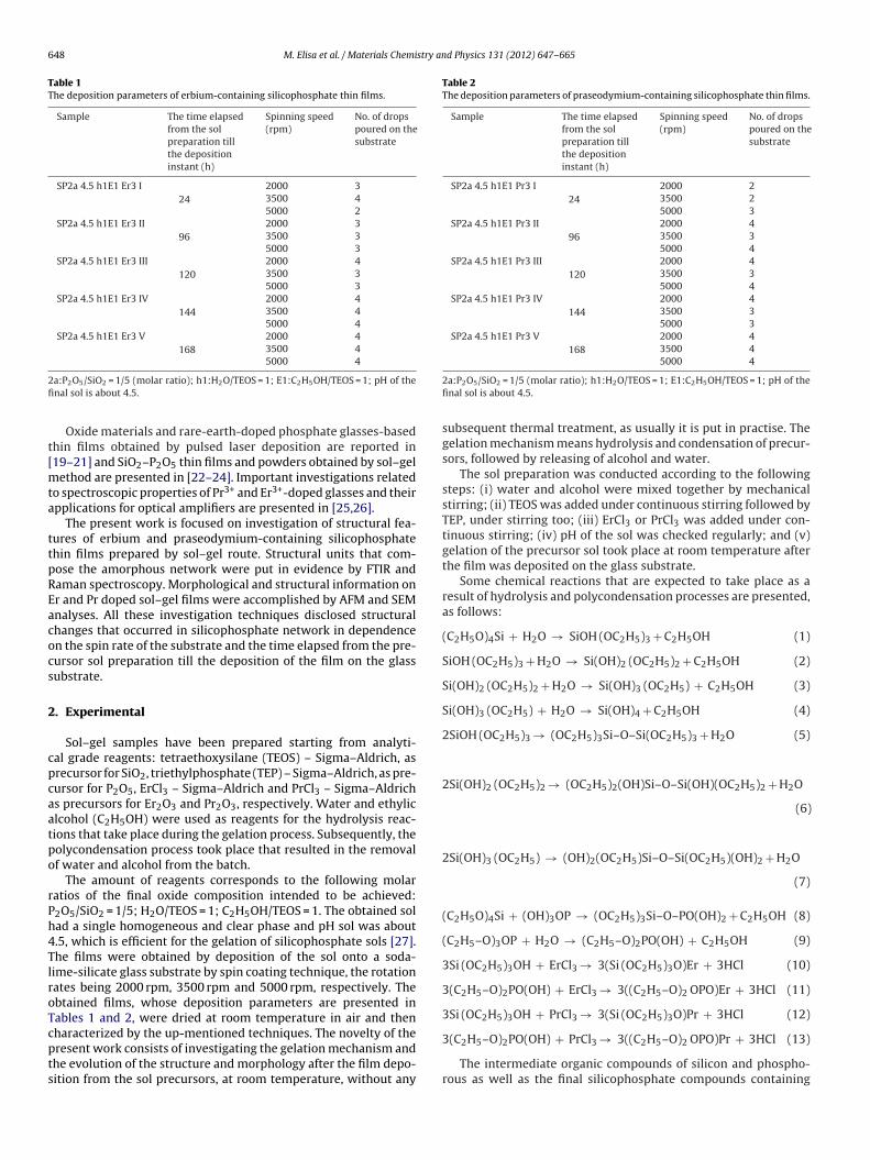
648 M. Elisa et al. / Materials Chemistry and Physics 131 (2012) 647– 665
Table 1The deposition parameters of erbium-containing silicophosphate thin films.
Sample The time elapsedfrom the solpreparation tillthe depositioninstant (h)
Spinning speed(rpm)
No. of dropspoured on thesubstrate
SP2a 4.5 h1E1 Er3 I24
2000 33500 45000 2
SP2a 4.5 h1E1 Er3 II96
2000 33500 35000 3
SP2a 4.5 h1E1 Er3 III120
2000 43500 35000 3
SP2a 4.5 h1E1 Er3 IV144
2000 43500 45000 4
SP2a 4.5 h1E1 Er3 V168
2000 43500 45000 4
2fi
t[mta
ttpREacocs
2
cpcaatpo
rPh4TlroTcpts
Table 2The deposition parameters of praseodymium-containing silicophosphate thin films.
Sample The time elapsedfrom the solpreparation tillthe depositioninstant (h)
Spinning speed(rpm)
No. of dropspoured on thesubstrate
SP2a 4.5 h1E1 Pr3 I24
2000 23500 25000 3
SP2a 4.5 h1E1 Pr3 II96
2000 43500 35000 4
SP2a 4.5 h1E1 Pr3 III120
2000 43500 35000 4
SP2a 4.5 h1E1 Pr3 IV144
2000 43500 35000 3
SP2a 4.5 h1E1 Pr3 V168
2000 43500 45000 4
a:P2O5/SiO2 = 1/5 (molar ratio); h1:H2O/TEOS = 1; E1:C2H5OH/TEOS = 1; pH of thenal sol is about 4.5.
Oxide materials and rare-earth-doped phosphate glasses-basedhin films obtained by pulsed laser deposition are reported in19–21] and SiO2–P2O5 thin films and powders obtained by sol–gel
ethod are presented in [22–24]. Important investigations relatedo spectroscopic properties of Pr3+ and Er3+-doped glasses and theirpplications for optical amplifiers are presented in [25,26].
The present work is focused on investigation of structural fea-ures of erbium and praseodymium-containing silicophosphatehin films prepared by sol–gel route. Structural units that com-ose the amorphous network were put in evidence by FTIR andaman spectroscopy. Morphological and structural information onr and Pr doped sol–gel films were accomplished by AFM and SEMnalyses. All these investigation techniques disclosed structuralhanges that occurred in silicophosphate network in dependencen the spin rate of the substrate and the time elapsed from the pre-ursor sol preparation till the deposition of the film on the glassubstrate.
. Experimental
Sol–gel samples have been prepared starting from analyti-al grade reagents: tetraethoxysilane (TEOS) – Sigma–Aldrich, asrecursor for SiO2, triethylphosphate (TEP) – Sigma–Aldrich, as pre-ursor for P2O5, ErCl3 – Sigma–Aldrich and PrCl3 – Sigma–Aldrichs precursors for Er2O3 and Pr2O3, respectively. Water and ethyliclcohol (C2H5OH) were used as reagents for the hydrolysis reac-ions that take place during the gelation process. Subsequently, theolycondensation process took place that resulted in the removalf water and alcohol from the batch.
The amount of reagents corresponds to the following molaratios of the final oxide composition intended to be achieved:2O5/SiO2 = 1/5; H2O/TEOS = 1; C2H5OH/TEOS = 1. The obtained solad a single homogeneous and clear phase and pH sol was about.5, which is efficient for the gelation of silicophosphate sols [27].he films were obtained by deposition of the sol onto a soda-ime-silicate glass substrate by spin coating technique, the rotationates being 2000 rpm, 3500 rpm and 5000 rpm, respectively. Thebtained films, whose deposition parameters are presented inables 1 and 2, were dried at room temperature in air and then
haracterized by the up-mentioned techniques. The novelty of theresent work consists of investigating the gelation mechanism andhe evolution of the structure and morphology after the film depo-ition from the sol precursors, at room temperature, without any2a:P2O5/SiO2 = 1/5 (molar ratio); h1:H2O/TEOS = 1; E1:C2H5OH/TEOS = 1; pH of thefinal sol is about 4.5.
subsequent thermal treatment, as usually it is put in practise. Thegelation mechanism means hydrolysis and condensation of precur-sors, followed by releasing of alcohol and water.
The sol preparation was conducted according to the followingsteps: (i) water and alcohol were mixed together by mechanicalstirring; (ii) TEOS was added under continuous stirring followed byTEP, under stirring too; (iii) ErCl3 or PrCl3 was added under con-tinuous stirring; (iv) pH of the sol was checked regularly; and (v)gelation of the precursor sol took place at room temperature afterthe film was deposited on the glass substrate.
Some chemical reactions that are expected to take place as aresult of hydrolysis and polycondensation processes are presented,as follows:
(C2H5O)4Si + H2O → SiOH (OC2H5)3 + C2H5OH (1)
SiOH (OC2H5)3 + H2O → Si(OH)2 (OC2H5)2 + C2H5OH (2)
Si(OH)2 (OC2H5)2 + H2O → Si(OH)3 (OC2H5) + C2H5OH (3)
Si(OH)3 (OC2H5) + H2O → Si(OH)4 + C2H5OH (4)
2SiOH (OC2H5)3 → (OC2H5)3Si–O–Si(OC2H5)3 + H2O (5)
2Si(OH)2 (OC2H5)2 → (OC2H5)2(OH)Si–O–Si(OH)(OC2H5)2 + H2O
(6)
2Si(OH)3 (OC2H5) → (OH)2(OC2H5)Si–O–Si(OC2H5)(OH)2 + H2O
(7)
(C2H5O)4Si + (OH)3OP → (OC2H5)3Si–O–PO(OH)2 + C2H5OH (8)
(C2H5–O)3OP + H2O → (C2H5–O)2PO(OH) + C2H5OH (9)
3Si (OC2H5)3OH + ErCl3 → 3(Si (OC2H5)3O)Er + 3HCl (10)
3(C2H5–O)2PO(OH) + ErCl3 → 3((C2H5–O)2 OPO)Er + 3HCl (11)
3Si (OC2H5)3OH + PrCl3 → 3(Si (OC2H5)3O)Pr + 3HCl (12)
3(C2H5–O)2PO(OH) + PrCl3 → 3((C2H5–O)2 OPO)Pr + 3HCl (13)
The intermediate organic compounds of silicon and phospho-rous as well as the final silicophosphate compounds containing

M. Elisa et al. / Materials Chemistry and Physics 131 (2012) 647– 665 649
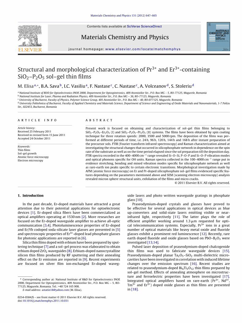
F um iop ining
Er
Ss4o
spm
ig. 1. FTIR spectra (400–2400 cm−1) of silicophosphate thin films containing erbireparation; (f): FTIR spectra (2400–4000 cm−1) of silicophosphate thin films conta
r or Pr are formed after releasing of water and organic volatileesidues.
FTIR spectra were recorded with a Perkin Elmerpectrophotometer-Spectrum 100, provided with UATR acces-ory (Universal Attenuated Total Reflectance) in the range00–4000 cm−1. The measurement error is ±0.1% and the numberf scans 32.
Raman spectra have been collected with a NRS-3100 JASCOpectrophotometer equipped with a laser emitting at 532 nm, laserower 18–35 mW, 60 accumulations, resolution 1 cm−1, measure-ent range 100–4000 cm−1.
ns, deposited after 24 h (a), 96 h (b), 120 h (c), 144 h (d) and 168 h (e) since the solerbium ions, deposited after 24 h.
In order to investigate the topography and the homogeneityof the films, an INTEGRA Prima atomic force microscope witha lateral resolution 0.2 nm and vertical resolution 0.04 nm wasused. The linear errors were ±0.5%. During the scanning process,the environmental vibrations in the 0.7–1000 Hz range have beenremoved.
The morphology of the films have been revealed by SEM images
recorded by means of a Hitachi S-2600N electronic microscopeequipped with energy dispersive X-ray spectrometer, with a res-olution of 5 nm, at different magnifications of 30×, 1500×, 3000×,5000×.
650 M. Elisa et al. / Materials Chemistry and Physics 131 (2012) 647– 665
F eodymF ium io
3
fi
p
s
ig. 2. FTIR spectra (400–2400 cm−1) of silicophosphate thin films containing prasTIR spectra (2400–4000 cm−1) of silicophosphate thin films containing praseodym
. Results
FTIR spectra of SiO2–P2O5–Er2O3 and of SiO2–P2O5–Pr2O3 thinlms are presented in Figs. 1 and 2, respectively.
The assignment of absorption peaks was made based on datarovided by [28–30] shown in Tables 3 and 4.
Raman spectra of SiO2–P2O5–Er2O3 thin films are pre-ented in Fig. 3, in dependence on the time elapsed from
ium ions, deposited after 24 h (a), 96 h (b), 120 h (c), 144 h (d) and 168 h (e); (f):ns, deposited after 24 h.
the instant of the sol preparation till the film deposi-tion moment as well as on the rotation speed of thesubstrate. The assignment of Raman peaks is given inTable 5.
Raman spectra of SiO2–P2O5–Pr2O3 thin films are presented inFig. 4. The same experimental conditions as in the case of erbium-containing films were used for these films. The assignment ofRaman peaks is shown in Table 6.
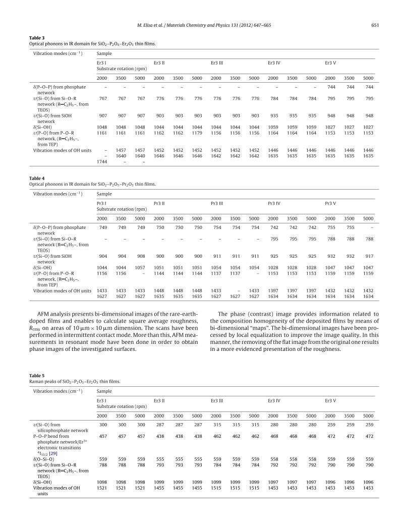
M. Elisa et al. / Materials Chemistry and Physics 131 (2012) 647– 665 651
Table 3Optical phonons in IR domain for SiO2–P2O5–Er2O3 thin films.
Vibration modes (cm−1) Sample
Er3 I Er3 II Er3 III Er3 IV Er3 VSubstrate rotation (rpm)
2000 3500 5000 2000 3500 5000 2000 3500 5000 2000 3500 5000 2000 3500 5000
ı(P–O–P) from phosphatenetwork
– – – – – – – – – – – – 744 744 744
�(Si–O) from Si–O–Rnetwork (R C2H5–, fromTEOS)
767 767 767 776 776 776 776 776 776 784 784 784 795 795 795
�(Si–O) from SiOHnetwork
907 907 907 903 903 903 903 903 903 935 935 935 948 948 948
ı(Si–OH) 1048 1048 1048 1044 1044 1044 1044 1044 1044 1059 1059 1059 1027 1027 1027�(P–O) from P–O–R
network, (R C2H5–,from TEP)
1161 1161 1161 1162 1162 1179 1156 1156 1156 1164 1164 1164 1153 1153 1153
Vibration modes of OH units – 1457 1457 1452 1452 1452 1452 1452 1452 1446 1446 1446 1446 1446 1446– 1640 1640 1646 1646 1646 1642 1642 1642 1635 1635 1635 1635 1635 1635
1744 – –
Table 4Optical phonons in IR domain for SiO2–P2O5–Pr2O3 thin films.
Vibration modes (cm−1) Sample
Pr3 I Pr3 II Pr3 III Pr3 IV Pr3 VSubstrate rotation (rpm)
2000 3500 5000 2000 3500 5000 2000 3500 5000 2000 3500 5000 2000 3500 5000
ı(P–O–P) from phosphatenetwork
749 749 749 750 750 750 754 754 754 742 742 742 755 755 –
�(Si–O) from Si–O–Rnetwork (R C2H5–, fromTEOS)
– – – – – – – – – 795 795 795 788 788 788
�(Si–O) from SiOHnetwork
904 904 908 900 900 900 911 911 911 925 925 925 932 932 917
ı(Si–OH) 1044 1044 1057 1051 1051 1051 1054 1054 1054 1028 1028 1028 1047 1047 1047�(P–O) from P–O–R
network, (R C2H5–,1156 1156 – 1144 1144 1144 1137 1137 – 1153 1153 1153 1159 1159 1159
8
5
dRpsp
TR
from TEP)Vibration modes of OH units 1433 1433 1433 1448 1448 144
1627 1627 1627 1635 1635 163
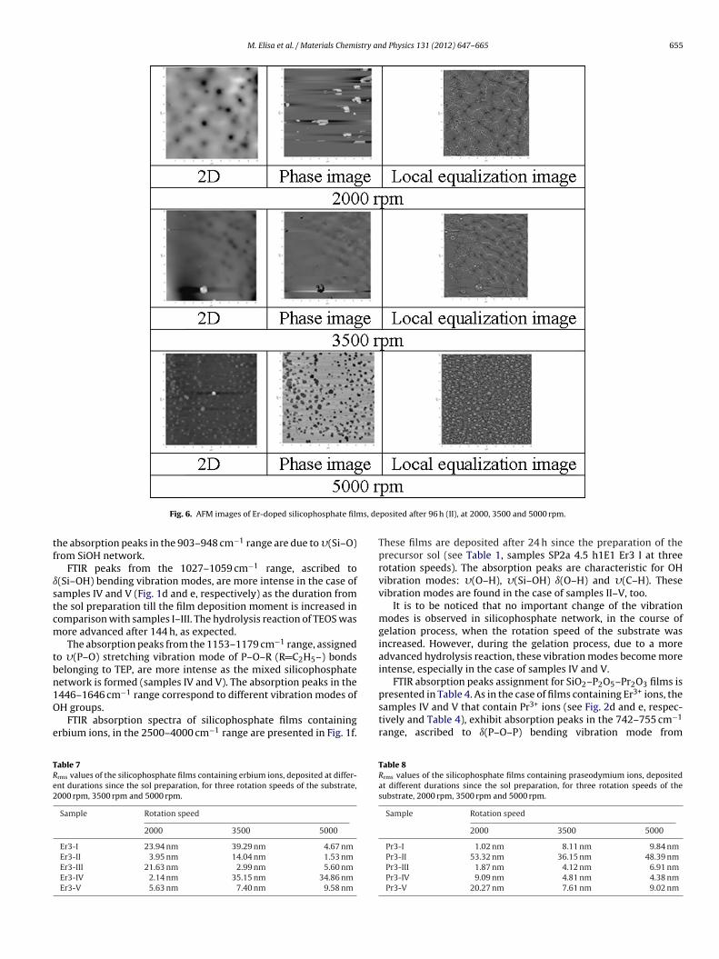
AFM analysis presents bi-dimensional images of the rare-earth-oped films and enables to calculate square average roughness,rms on areas of 10 �m × 10 �m dimension. The scans have been
erformed in intermittent contact mode. More than this, AFM mea-urements in resonant mode have been done in order to obtainhase images of the investigated surfaces.able 5aman peaks of SiO2–P2O5–Er2O3 thin films.
Vibration modes (cm−1) Sample
Er3 I Er3 II
Substrate rotation (rpm)
2000 3500 5000 2000 3500 5000
�(Si–O) fromsilicophosphate network
300 300 300 287 287 287
P–O–P bend fromphosphate network/Er3+
electronic transitions4I15/2 [29]
457 457 457 438 438 438
ı(O–Si–O) 559 559 559 555 555 555
�(Si–O) from Si–O–Rnetwork (R C2H5–, fromTEOS)
788 788 788 793 793 793
ı(Si–OH) 1098 1098 1098 1099 1099 1099
Vibration modes of OHunits
1521 1521 1521 1455 1455 1455
1433 – 1433 1397 1397 1397 1432 1432 14321627 1627 1627 1634 1634 1634 1634 1634 1634
The phase (contrast) image provides information related tothe composition homogeneity of the deposited films by means ofbi-dimensional “maps”. The bi-dimensional images have been pro-
cessed by local equalization to improve the image quality. In thismanner, the removing of the flat image from the original one resultsin a more evidenced presentation of the roughness.Er3 III Er3 IV Er3 V
2000 3500 5000 2000 3500 5000 2000 3500 5000
315 315 315 280 280 280 259 259 259
462 462 462 468 468 468 472 472 472
559 559 559 558 558 558 559 559 559784 784 784 792 792 792 790 790 790
1099 1099 1099 1097 1097 1097 1096 1096 10961515 1515 1515 1453 1453 1453 1453 1453 1453

652 M. Elisa et al. / Materials Chemistry and Physics 131 (2012) 647– 665
F ium ip
nc3pp
fiu2
ig. 3. Raman spectra (100–4000 cm−1) of silicophosphate thin films containing erbreparation.
In Table 7, the values of the square average rough-ess, Rrms are presented, in the case of silicophosphate filmsontaining erbium ions for three rotation speeds: 2000 rpm,500 rpm and 5000 rpm. In Figs. 5–9, AFM images (sam-les I–V) of the films from the SiO2–P2O5–Er2O3 system areresented.
AFM measurements have also been done on SiO2–P2O5–Pr2O3lms prepared by sol–gel method. In Table 8, the Rrms val-es for these films are reported for three rotation rates:000 rpm, 3500 rpm and 5000 rpm. In Figs. 10–14, AFM images
ons, deposited after 24 h (a), 96 h (b), 120 h (c), 144 h (d) and 168 h (e) since the sol
(samples I–V) of the films from the SiO2–P2O5–Pr2O3 system arepresented.
Microstructural analysis by scanning electron microscopy (SEM)have been done on sol–gel Er and Pr-doped silicophosphate filmswith similar deposition parameters: SiO2/P2O5 ratio being 1/5,rare earth oxide (Er2O3 or Pr2O3) 3% mol., the rotation rate of
the substrate being 2000 rpm, at different time intervals since thepreparation of the sol: 24, 96, 120, 144 and, respectively, 168 h. Forall the deposited films, special features were put in evidence, someof them being clearly visible at submicron and/or micron scale.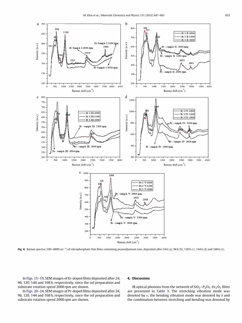
M. Elisa et al. / Materials Chemistry and Physics 131 (2012) 647– 665 653
Fig. 4. Raman spectra (100–4000 cm−1) of silicophosphate thin films containing praseodymium ions, deposited after 24 h (a), 96 h (b), 120 h (c), 144 h (d) and 168 h (e).
9s
9s
In Figs. 15–19, SEM images of Er-doped films deposited after 24,6, 120, 144 and 168 h, respectively, since the sol preparation and
ubstrate rotation speed 2000 rpm are shown.In Figs. 20–24, SEM images of Pr-doped films deposited after 24,6, 120, 144 and 168 h, respectively, since the sol preparation andubstrate rotation speed 2000 rpm are shown.
4. Discussion
IR optical phonons from the network of SiO2–P2O5–Er2O3 filmsare presented in Table 3. The stretching vibration mode wasdenoted by �, the bending vibration mode was denoted by ı andthe combination between stretching and bending was denoted by
654 M. Elisa et al. / Materials Chemistry and Physics 131 (2012) 647– 665
Table 6Raman peaks of SiO2–P2O5–Pr2O3 thin films.
Vibration modes (cm−1) Sample
Pr3 I Pr3 II Pr3 III Pr3 IV Pr3 VSubstrate rotation (rpm)
2000 3500 5000 2000 3500 5000 2000 3500 5000 2000 3500 5000 2000 3500 5000
�(Si–O) fromsilicophosphate network
337 337 337 266 266 266 280 280 280 266 266 266 294 294 294
P–O–P bend fromphosphate network/Pr3+
electronic transitions3H4 [29]
468 468 468 456 456 456 476 476 476 459 459 459 458 458 458
ı(O–Si–O)/Pr3+ electronictransitions 3H4 [29]
560 560 560 557 557 557 559 559 559 557 557 557 561 561 561
�(Si–O) from Si–O–Rnetwork (R C2H5–, fromTEOS)
780 780 780 784 784 784 794 794 794 780 780 780 797 797 797
5
6
ωavihI
ı(Si–OH) 1100 1100 1100 1095 1095 109Vibration modes of OH
units1517 1517 1517 1516 1516 151
[28]. In the case of the film V (see Fig. 1e), it is to be noticedbsorption peaks at 744 cm−1, attributed to ı(P–O–P) bending
ibration modes from phosphate network. These absorption max-ma are characteristic for silicophosphate network as a result ofydrolysis–condensation reactions that take place in the system.n the case of samples I–IV (Fig. 1a–d, respectively), deposited at
Fig. 5. AFM images of Er-doped silicophosphate films, de
1097 1097 1097 1095 1095 1095 1097 1097 10971592 1592 1592 1514 1514 1514 1416 1416 1416
shorter time intervals versus the moment of the sol preparation,the up-mentioned absorption peaks were not observed. It is sup-
posed that for samples I–IV, hydrolysis–condensation reactions arein an incipient stage.The absorption peaks in the 767–795 cm−1 range (Fig. 1a–e) aredue to �(Si–O) from Si–O–R network (R C2H5–, from TEOS) and
posited after 24 h (I), at 2000, 3500 and 5000 rpm.
M. Elisa et al. / Materials Chemistry and Physics 131 (2012) 647– 665 655
s, de
tf
ıstcm
tbn1O
e
TRe2
Fig. 6. AFM images of Er-doped silicophosphate film
he absorption peaks in the 903–948 cm−1 range are due to �(Si–O)rom SiOH network.
FTIR peaks from the 1027–1059 cm−1 range, ascribed to(Si–OH) bending vibration modes, are more intense in the case ofamples IV and V (Fig. 1d and e, respectively) as the duration fromhe sol preparation till the film deposition moment is increased inomparison with samples I–III. The hydrolysis reaction of TEOS wasore advanced after 144 h, as expected.The absorption peaks from the 1153–1179 cm−1 range, assigned
o �(P–O) stretching vibration mode of P–O–R (R C2H5–) bondselonging to TEP, are more intense as the mixed silicophosphateetwork is formed (samples IV and V). The absorption peaks in the
−1
446–1646 cm range correspond to different vibration modes ofH groups.FTIR absorption spectra of silicophosphate films containingrbium ions, in the 2500–4000 cm−1 range are presented in Fig. 1f.
able 7rms values of the silicophosphate films containing erbium ions, deposited at differ-nt durations since the sol preparation, for three rotation speeds of the substrate,000 rpm, 3500 rpm and 5000 rpm.
Sample Rotation speed
2000 3500 5000
Er3-I 23.94 nm 39.29 nm 4.67 nmEr3-II 3.95 nm 14.04 nm 1.53 nmEr3-III 21.63 nm 2.99 nm 5.60 nmEr3-IV 2.14 nm 35.15 nm 34.86 nmEr3-V 5.63 nm 7.40 nm 9.58 nm
posited after 96 h (II), at 2000, 3500 and 5000 rpm.
These films are deposited after 24 h since the preparation of theprecursor sol (see Table 1, samples SP2a 4.5 h1E1 Er3 I at threerotation speeds). The absorption peaks are characteristic for OHvibration modes: �(O–H), �(Si–OH) ı(O–H) and �(C–H). Thesevibration modes are found in the case of samples II–V, too.
It is to be noticed that no important change of the vibrationmodes is observed in silicophosphate network, in the course ofgelation process, when the rotation speed of the substrate wasincreased. However, during the gelation process, due to a moreadvanced hydrolysis reaction, these vibration modes become moreintense, especially in the case of samples IV and V.
FTIR absorption peaks assignment for SiO2–P2O5–Pr2O3 films is3+
presented in Table 4. As in the case of films containing Er ions, thesamples IV and V that contain Pr3+ ions (see Fig. 2d and e, respec-tively and Table 4), exhibit absorption peaks in the 742–755 cm−1
range, ascribed to ı(P–O–P) bending vibration mode from
Table 8Rrms values of the silicophosphate films containing praseodymium ions, depositedat different durations since the sol preparation, for three rotation speeds of thesubstrate, 2000 rpm, 3500 rpm and 5000 rpm.
Sample Rotation speed
2000 3500 5000
Pr3-I 1.02 nm 8.11 nm 9.84 nmPr3-II 53.32 nm 36.15 nm 48.39 nmPr3-III 1.87 nm 4.12 nm 6.91 nmPr3-IV 9.09 nm 4.81 nm 4.38 nmPr3-V 20.27 nm 7.61 nm 9.02 nm

656 M. Elisa et al. / Materials Chemistry and Physics 131 (2012) 647– 665
s, dep
pct
easeI
�s
ısa1aph
�Titv
s
Fig. 7. AFM images of Er-doped silicophosphate film
hosphate network. These vibration modes are not observed in thease of samples I–III containing Pr3+ ions. The explanation is similaro that of Er3+-containing samples.
The absorption peaks in the 788–795 cm−1 range (Fig. 2d and) are due to �(Si–O) from Si–O–R network (R C2H5–, from TEOSnd TEP). These absorption maxima are not observed in the case ofamples I, II and III (see Fig. 2a–c, respectively). This fact could bexplained by the advanced hydrolysis process in the case of samplesV and V as compared to samples I–III.
The absorption peaks in the 900–932 cm−1 range are assigned to(Si–O) from SiOH network, which are found in all Pr3+-containing
amples.The peaks from the 1028–1057 cm−1 range, attributed to
(Si–OH) bending vibration mode are noticed in the spectra ofamples I–V. The explanation of the presence of more intensebsorption maxima in the case of samples IV and V, 1028 cm−1 and047 cm−1 is similar to that presented in the case of samples IVnd V containing Er3+. As the time elapsed since the precursor solreparation till the instant of the film deposition was increased, theydrolysis was more advanced and more OH groups were formed.
The absorption peaks in the 1137–1159 cm−1 range, assigned to(P–O) stretching vibration mode from P–O–R (R C2H5–) bond ofEP become more intense as silicophosphate network is formed,n the case of samples IV and V containing Pr3+ ions. The absorp-
ion peaks in the 1397–1635 cm−1 range correspond to differentibration modes of OH groups.FTIR absorption spectra in the 2500–4000 cm−1 range are pre-ented in Fig. 2f, in the case of silicophosphate films containing Pr3+
osited after 120 h (III), at 2000, 3500 and 5000 rpm.
ions, deposited short time after the preparation of the precursor sol(see Table 2, samples SP2a 4.5 h1E1 Pr3 I at three rotation speeds).The absorption peaks are characteristic to different vibration modesof OH group such as �(O–H), �(Si–OH) and ı(O–H) bonds. Thesevibration modes are also noticed in the case of samples II–V.
Similar to the samples containing Er3+ ions, in the case ofPr3+-containing samples, no significant modification of the vibra-tion modes were revealed when the substrate rotation speed wasincreased. This last parameter does not significantly influence theintensity of absorption peaks in the case of samples I–III, containingPr3+ ions, due to a relative less advanced hydrolysis process of thedeposited sol. As the viscosity of the precursor sol is increased, inthe case of samples IV and V, the influence of the substrate rota-tion speed on the intensity of vibration modes is also increased.This is due to a more advanced hydrolysis reaction as in the case ofEr3+-containing samples.
The assignment of Raman peaks for SiO2–P2O5–Er2O3 films ispresented in Table 5. It is to be noticed (see Fig. 3a–e) those Ramanspectra revealed mainly specific peaks to P–O–P, Si–O, O–Si–O andSi–OH bonds vibration modes. Raman peaks from 457 to 472 cm−1
range are assigned to P–O–P bend from phosphate network and/orto 4I15/2 electronic transition of Er3+ ions, according to [31]. Aspresented in Fig. 3, no obvious influence of the rotation speed onnetwork vibration modes was disclosed.
The peaks noticed over 2400 cm−1 are attributed to the fol-lowing vibration modes: �(P–H) from the reaction between(RO)xPO(OH)y and alkyl groups, �(O P–OH) from O P–OH and sin-gle OH groups and �(P–OH) from P–OH bonds.

M. Elisa et al. / Materials Chemistry and Physics 131 (2012) 647– 665 657
s, dep
sePRbPmPsnvs
pfitd
sbIire
ti
Fig. 8. AFM images of Er-doped silicophosphate film
Raman peaks assignment for SiO2–P2O5–Pr2O3 films is pre-ented in Table 6. As in the case of Raman spectra ofrbium-containing films, the main revealed Raman peaks are due to–O–P, Si–O, O–Si–O and Si–OH bonds vibration modes (Fig. 4a–e).aman peaks from 468 to 476 cm−1 range are assigned to P–O–Pend from phosphate network and/or to 3H4 electronic transition ofr3+ ions, according to [31]. In the 557–561 cm−1 interval, Ramanaxima due to ı(O–Si–O) and/or to 3H4 electronic transition of
r3+are noticed [31]. One can observe that the influence of sub-trate rotation speed on the intensity and position of these peaks isot significant. The peaks found over 2400 cm−1 are due to differentibration modes that implies OH groups, as in the case of Ramanpectra for erbium-containing samples.
AFM search aims at investigating the changes of the topogra-hy and homogeneity of the surface of Er/Pr-doped silicophosphatelms in dependency on the rotation speeds of the substrate andhe time elapsed since the preparation of the precursor sol till theeposition moment.
Er-doped silicophosphate films obtained by sol–gel method,pin coating technique are uniform and homogeneous as revealedoth by AFM phase images (Figs. 5–9) and Rrms values (see Table 7).
t is to notice a different behavior of the films topography depend-ng on the rotation rate in the deposition stage. At certain rotationates an improved chemical homogeneity, a low roughness and
ven some cavities are observed.From Fig. 5 (films deposited after 24 h since the sol prepara-ion) it is observed a decreased roughness when the rotation rates increased, accompanied by the apparition of some convex and
osited after 144 h (IV), at 2000, 3500 and 5000 rpm.
concave cavities having dimensions between tens and hundredsnanometers. As regards the chemical homogeneity, it is foundan improved homogeneity in the case of the film deposited at3500 rpm.
In the case of the Er-doped films deposited after 96 h since thesol preparation (see Fig. 6), one can observe some positive cavi-ties, uniformly distributed, with dimensions from tens to hundredsnanometers. It is noticed an improved compositional homogeneitywhen the rotation rate is raised at 3500 rpm similar with the caseof the film deposited after 24 h since the sol preparation.
From AFM images of Er-doped films deposited after 120 h (seeFig. 7), it is noticed the same behavior related to the improving ofthe homogeneity as regards the composition, at 3500 rpm rotationrate of the substrate.
In the case of Er-doped films deposited after 144 h (see Fig. 8)it is revealed a changed behavior as the homogeneity is improvedboth at 3500 rpm and 5000 rpm rotation rates.
The same improved chemical homogeneity is also observed inthe case of Er-doped films deposited after 168 h since the sol prepa-ration (see Fig. 9), at 3500 rpm and 2000 rpm, together with somecavities noticed at 5000 rpm.
It is to be concluded that the sol–gel films from theSiO2–P2O5–Er2O3 system, prepared at different durations sincethe sol preparation till the deposition moment exhibit a differ-
ent behavior depending on the rotation rate of the substrate. Itis revealed that the compositional homogeneity is improved at3500 rpm. Some cavities are observed in the films deposited at5000 rpm.
658 M. Elisa et al. / Materials Chemistry and Physics 131 (2012) 647– 665
s, dep
pfisih
etsgd
ar
fi
ai
aato
t
Fig. 9. AFM images of Er-doped silicophosphate film
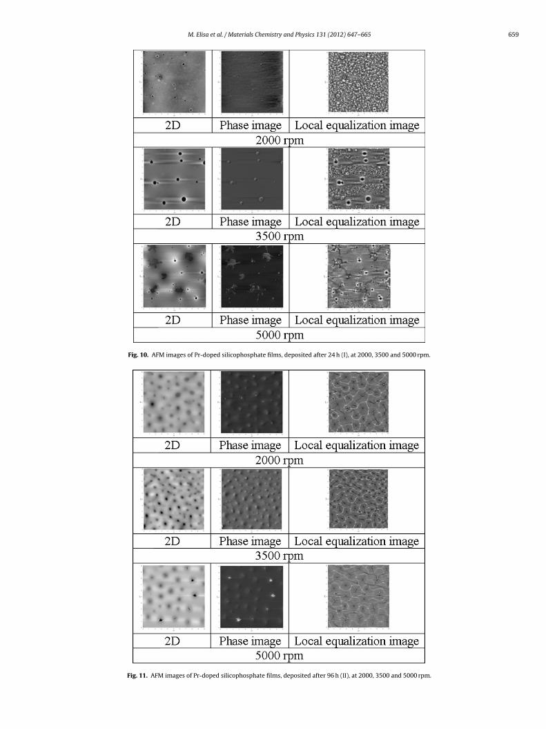
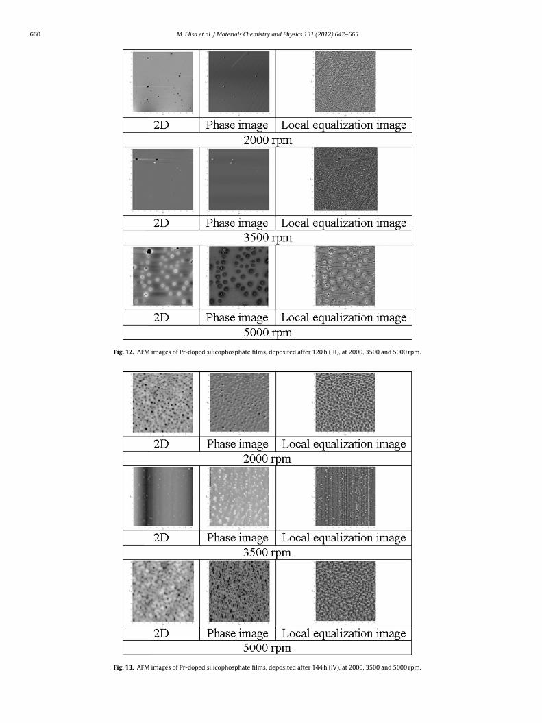
In the case of silicophosphate sol–gel films containingraseodymium ions, according to AFM images (Figs. 10–14), uni-orm and homogeneous films have been prepared as emphasizedn phase images and given by Rrms values. In contrast with Er-dopedilicophosphate films, in the case of the films with Pr ions, a crack-ng tendency is observed at high rotation rates besides a lack ofomogeneity as regards the chemical composition.
From Fig. 10, one can see that the films prepared at low durationlapsed from the sol preparation till the deposition moment, for allhree up-mentioned rotation rates, some cavities are found on theurface of the film. At higher rotation rates, the film is nonhomo-eneous as regards the composition in comparison with the filmseposited at 2000 rpm and 3500 rpm.
In the case of the films deposited after 96 h (Fig. 11), the cavitiesre observed on the surface of the samples for all three rotationates. Additionally, some cracks are found at 5000 rpm.
From Fig. 12, an intense lack of homogeneity is revealed for thelm deposited at 5000 rpm.
AFM images of the films deposited after 144 h (Fig. 13), revealed change of the aspect at 5000 rpm due to the chemical homogene-ty of the film.
Silicophosphate films containing praseodymium, depositedfter 168 h (Fig. 14), present a similar aspect as those depositedfter 144 h, with an improved chemical homogeneity at high rota-
ion rates. For all three rotation rates, the tendency to form cavitiesn the surface of the films is preserved.As a conclusion, the morphological analysis made by AFMechnique evidences specific characteristics depending on the
osited after 168 h (V), at 2000, 3500 and 5000 rpm.
rotation rate. Thus, at high rotation rates, a decrease of thechemical homogeneity is found and even some cracks areobserved on the surface of the films deposited bellow 120 hduration since the sol preparation. In the case of the filmsprepared at intervals of time higher than 120 h, an improve-ment of the homogeneity is observed, even at higher rotationrates.
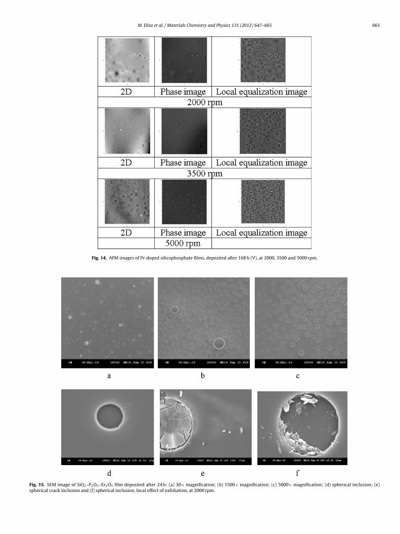
SEM analysis presents in Fig. 15a (30× magnification, scale1 mm) some formations of relative big dimensions (approx.10–20 �m), quasi-uniformly distributed together with roundedstructural units of micron dimensions. It is most probably thatthe noticed structures to be generated by the deposition process,trapping inside the gaseous phase. In supporting this supposition,the micrograph from Fig. 15b, corresponding to a magnificationof 1500× (scale of 10 �m), put in evidence ordered areas, withthe same image of the structures, which seems to contain gaseousinclusions of submicron size. The above-mentioned aspect is evi-dent at a higher magnification (5000×) of the same area, presentedin Fig. 15c. These gaseous inclusions can be subjected to a dehy-dration process, more intense in the upper side, i.e. the sphericaldome (see the detail from Fig. 15d). Due to the strains that appearduring the drying process, the spherical structures could be dam-aged, as it can be seen in Fig. 15e and f where an exfoliation effect isrevealed.
In Fig. 16, the SEM image obtained at the same magnification(30×, the scale of 1 mm) put in evidence a more flat surface incomparison with that observed in the case of the film depositedafter 24 h since the sol preparation, when the dehydration degree
M. Elisa et al. / Materials Chemistry and Physics 131 (2012) 647– 665 659
Fig. 10. AFM images of Pr-doped silicophosphate films, deposited after 24 h (I), at 2000, 3500 and 5000 rpm.
Fig. 11. AFM images of Pr-doped silicophosphate films, deposited after 96 h (II), at 2000, 3500 and 5000 rpm.
660 M. Elisa et al. / Materials Chemistry and Physics 131 (2012) 647– 665
Fig. 12. AFM images of Pr-doped silicophosphate films, deposited after 120 h (III), at 2000, 3500 and 5000 rpm.
Fig. 13. AFM images of Pr-doped silicophosphate films, deposited after 144 h (IV), at 2000, 3500 and 5000 rpm.
M. Elisa et al. / Materials Chemistry and Physics 131 (2012) 647– 665 661
Fig. 14. AFM images of Pr-doped silicophosphate films, deposited after 168 h (V), at 2000, 3500 and 5000 rpm.
Fig. 15. SEM image of SiO2–P2O5–Er2O3 film deposited after 24 h: (a) 30× magnification; (b) 1500× magnification; (c) 5000× magnification; (d) spherical inclusion; (e)spherical crack inclusion and (f) spherical inclusion, local effect of exfoliation, at 2000 rpm.

662 M. Elisa et al. / Materials Chemistry and Physics 131 (2012) 647– 665
Fig. 16. SEM image of SiO2–P2O5–Er2O3 film deposited after 96 h: (a) 30× magnification; (b) >30× magnification and (c) micro-cracks around the semispherical structures,at 2000 rpm.
Fig. 17. SEM image for SiO2–P2O5–Er2O3 film deposited after 120 h: (a) 30× magnification; (b) and (c) exfoliated semi-sphere structures and micro-cracks, at 2000 rpm.
Fig. 18. SEM image for SiO2–P2O5–Er2O3 film deposited after 144 h: (a) 30× magnification; (b) almost complete exfoliation of the semi-sphere caps and (c) semi-spherestructures inside of big dimensions semi-spheres, at 2000 rpm.
Fig. 19. SEM image of SiO2–P2O5–Er2O3 film deposited after 168 h: (a) 30× magnification and (b) cracking process accompanied by a general exfoliation tendency, at2000 rpm.
M. Elisa et al. / Materials Chemistry and Physics 131 (2012) 647– 665 663
agnifi
ws
dfb1tta
Ft
Fig. 20. SEM image of SiO2–P2O5–Pr2O3 film deposited after 24 h: (a) 30× m
as more reduced. Anyway, the same structures having roundedemi-sphere shapes are observed.
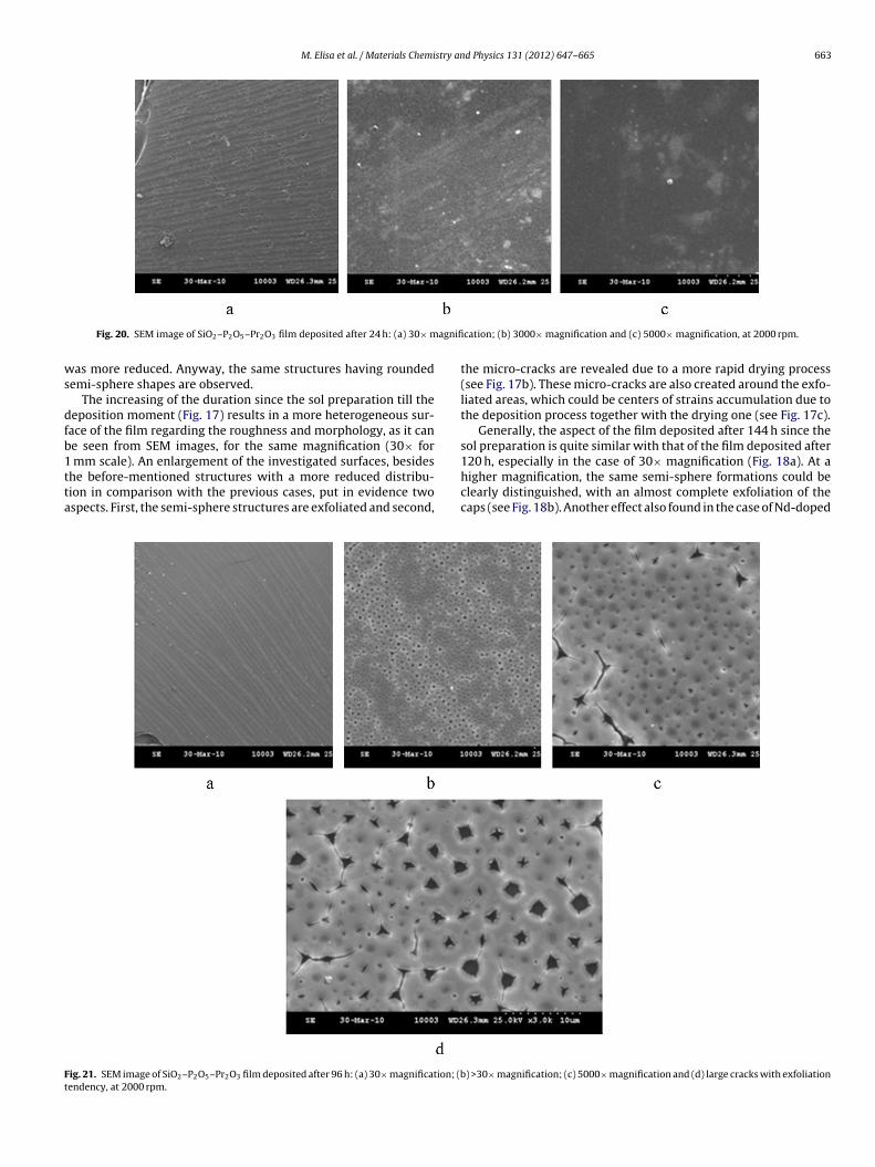
The increasing of the duration since the sol preparation till theeposition moment (Fig. 17) results in a more heterogeneous sur-ace of the film regarding the roughness and morphology, as it cane seen from SEM images, for the same magnification (30× for
mm scale). An enlargement of the investigated surfaces, besideshe before-mentioned structures with a more reduced distribu-ion in comparison with the previous cases, put in evidence twospects. First, the semi-sphere structures are exfoliated and second,
ig. 21. SEM image of SiO2–P2O5–Pr2O3 film deposited after 96 h: (a) 30× magnification; (bendency, at 2000 rpm.
cation; (b) 3000× magnification and (c) 5000× magnification, at 2000 rpm.
the micro-cracks are revealed due to a more rapid drying process(see Fig. 17b). These micro-cracks are also created around the exfo-liated areas, which could be centers of strains accumulation due tothe deposition process together with the drying one (see Fig. 17c).
Generally, the aspect of the film deposited after 144 h since thesol preparation is quite similar with that of the film deposited after
120 h, especially in the case of 30× magnification (Fig. 18a). At ahigher magnification, the same semi-sphere formations could beclearly distinguished, with an almost complete exfoliation of thecaps (see Fig. 18b). Another effect also found in the case of Nd-doped) >30× magnification; (c) 5000× magnification and (d) large cracks with exfoliation
664 M. Elisa et al. / Materials Chemistry and Physics 131 (2012) 647– 665
Fig. 22. SEM image of SiO2–P2O5–Pr2O3 film deposited after 120 h: (a) 30× magnification; (b) exfoliated semi-sphere structures and (c) exfoliated semi-sphere structuresand micro-cracks, at 2000 rpm.
F exfo
fiotdi
itmcApF
e
F
ig. 23. SEM image of SiO2–P2O5–Pr2O3 film deposited after 144 h: (a) cracking and
lms [30], is the apparition of submicron semi-sphere units insidef larger semi-spheres (Fig. 18c). These ones are visible in the case ofhe structures with semi-sphere cap completely damaged, possiblyue to the mixed effect of surface tension and mechanical tensions
nduced by the deposition process.The deposition process is influenced in a great extent by the
ncreasing of the elapsed duration since the preparation of the solill the deposition moment, namely 168 h. Thus, according to SEM
icrograph (see Fig. 19a), the surface of the deposited film exhibitsracks on its entire area, indication an advanced drying process.
higher magnification put in evidence the fact that the crackingrocess is accompanied by a general exfoliation as it is seen from
ig. 19b.In the case of Pr-doped films, SEM analysis revealed a very differ-nt behavior in comparison with the sol–gel silicophosphate films
ig. 24. SEM image of SiO2–P2O5–Pr2O3 film deposited after 168 h, at 2000 rpm.
liation of the film as regular small plates and (b) more detailed image, at 2000 rpm.
containing Er and Nd [32]. The surface of the film deposited after24 h since the sol preparation exhibits a very different topography.Thus, in Fig. 20a (30× magnification) a lot of oriented striations canbe seen, maybe pursuing the direction of the deposition of the film.The mechanism of the formation of the striations is not very clear,a systematic knowledge on the relationship between the striationsand the processing parameters is still lacking. Although, the maincauses that determine the formation of the striations are, on onehand the convection phenomena consisting in solvent evaporation,during the drying stage, contributing to the thinning of the film and,secondly, the increasing of the film roughness due to the decreasingof the substrate rotation speed and the increasing of the sol viscosity[33]. In the case of the samples deposited after 24 h and 96 h, thesol viscosity is low, leading to thinner films, which favor a fasterevaporation of the solvent and the apparition of the striations.
A higher resolution (3000×) puts in evidence a fibrous inter-stice structure and it is difficult to appreciate if there is a crystallinestructure or an amorphous one (see Fig. 20b). Inside of this fibrousformations, some islands structures can be distinguished (lightencolor in the micrograph) whose origin is not precisely estab-lished. In this direction, additional analyses are necessary as TEM(transmission electron microscopy) correlated with XRD (X-raydiffraction). The morphology of these formations is visible at ahigher magnification, 5000× (see Fig. 20c).
In the case of the film deposited after 96 h since the sol prepa-ration, SEM image indicates a quasi-oriented striations structure,seemingly similar to the previous Er-doped film, as it can be seenfrom Fig. 21a (30× magnification). The use of a better resolutionshows in evidence different lighten or darken areas corresponding
to different morphology aspects (see Fig. 21b). The detailed analysisof each zone (5000× magnification) revealed a structural arrange-ment composed of darken areas having a relative compact structure
stry an
cam
ifiec
pcof
cb
5
vRnPciwtotit
pnwia
ecddm
A
aof
[
[[[[[
[
[
[
[
[
[
[
[
[
[[
[
[[[
M. Elisa et al. / Materials Chemi
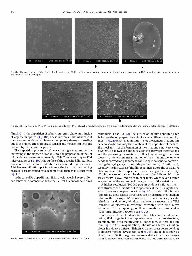
haracterized by submicron crater areas, seemingly without cracks,s it is disclosed in Fig. 21c. The adjoining lightens areas presenticron cracks, with an evident exfoliation tendency (Fig. 21d).The topography of the surface of the films deposited after 120 h
s practically similar to that of Nd-doped film [32] and Er-dopedlm, having the same morphology and superficial aspect. This isvident from Fig. 22a–c and the discussion is similar to the previousase of Er-doped film deposited after 120 h.
In the case of the film deposited after 144 h, the behavior is com-letely different in comparison with the previous cases. An intenseracking effect is noticed accompanied by an enhanced exfoliationf the film as small plates with regular shapes, as it can be seenrom Fig. 23a. A more detailed image is presented in Fig. 23b.
The SEM image of the film deposited after 168 h exhibits manyracks (see Fig. 24), the interface between the two adjacent zoneseing easily distinguished.
. Conclusions
FTIR spectra put in evidence stretching, bending and mixedibration modes specific to Si–O, P–O, Si–O–P and OH groups.aman spectra revealed mainly peaks specific to silicophosphateetwork and to certain electronic transitions specific to Er3+ andr3+ ions. No important changes of the peaks intensity and positionould be observed when the substrate rotation speed was mod-fied. AFM analysis revealed that Er-doped silicophosphate films
ere relatively uniform in thickness and chemically homogeneous,hese features depending on the spinning rate of the substrate andn the duration elapsed since the sol preparation till the deposi-ion moment. It is revealed that the compositional homogeneity ismproved at 3500 rpm, some cavities being observed in the case ofhe films deposited at 5000 rpm.
As regards the silicophosphate sol–gel films containingraseodymium ions, AFM images present uniform and homoge-eous films as the phase images and Rrms values show. In contrastith Er-doped silicophosphate films, in the case of the films with Pr
ons, a cracking tendency is observed at high rotation rates besides lack of homogeneity as regards the chemical composition.
SEM analysis put in evidence micron sphere structures,xfoliation and micro-cracks with different peculiarities in thease of Er-doped films in comparison with Pr-doped films,epending on the spinning rate of the substrate and on theuration elapsed since the sol preparation till the depositionoment.
cknowledgements
The authors are grateful to National Center for Programs Man-gement – Partnerships for the financial support in the framef 71-054/2007 contract and to Romanian Executive Agencyor Higher Education and Research Funding for the financial
[[
[
d Physics 131 (2012) 647– 665 665
support in the frame of PN 09-27.02.02/27.02.2009 (Nucleus Pro-gram 2009–2011).
References
[1] F. Gourbilleau, C. Dufour, M. Levalois, J. Vicens, R. Rizk, C. Sada, F. Enrichi, G.Battaglin, J. Appl. Phys. 94 (2003) 3869.
[2] C.Y. Chen, W.D. Chen, S.F. Song, Z.J. Xu, X.B. Liao, G.H. Li, K. Ding, J. Appl. Phys.94 (2003) 5599.
[3] L.H. Slooff, J. Appl. Phys. 91 (2002) 3955.[4] J.H. Yang, S.X. Dai, Y.F. Zhou, L. Wen, L.L. Hu, Z.H. Jiang, J. Appl. Phys. 93 (2003)
977.[5] S.F. Li, Q.Y. Zhang, Y.P. Lee, J. Appl. Phys. 96 (9) (2004) 4746–4750.[6] C.C. Santos, I. Guedes, C.-K. Loong, L.A. Boatner, A.L. Moura, M.T. de Araujo, C.
Jacinto, M.V.D. Vermelho, J. Phys. D Appl. Phys. 43 (2) (2010), doi:10.1088/0022-3727/43/2/025102.
[7] G. Gang, D. Youwei, Y. Tsing, Thin Solid Films 315 (1–2) (1998) 263–265.[8] C. Urlacher, C. Marco de Lucas, E. Bernstein, B. Jacquier, J. Mugnier, Opt. Mater.
12 (1999) 19–25.[9] M.F. Cerqueira, T. Monteiro, M.J. Soares, A. Kozanecki, P. Alpuim, E. Alves, Phys.
Status Solidi C 7 (3–4) (2010) 683–687.10] S. Yliniemia, J. Albert, A. Laronche, Q. Wang, S. Honkanen, Proc. SPIE 6183 (2006)
61830M.11] W.A Pisarski, J. Opt. Adv. Mater. 8 (3) (2006) 1206–1210.12] W.A. Pisarski, J. Mol. Struct. 473 (2005) 744–747.13] B. Karthikeyan, S. Mohan, Physica B 334 (2003) 298.14] B. Karthikeyan, Reji Philip, S. Mohan, Opt. Commun. 246 (2005) 153.15] M. De Sario, G. Leggieri, A. Luches, M. Martino, F. Prudenzano, A. Rizzo, Appl.
Surf. Sci. 186 (1–4) (2002) 216–220.16] A. Belarouci, B. Jacquier, P. Moretti, S. Robert, H. Rigneault, J. Opt. Soc. Am. B 18
(6) (2001) 832–838.17] H.Z. Chen, M.C. Kao, S.L. Young, C.C. Yu, C.H. Lin, C.M. Lee, C.R. Ou, Thin Solid
Films 517 (17) (2009) 4818–4821.18] G.C. Righini, M. Brenci, G.N. Conti, S. Pelli, M. Ferrari, M. Bettinelli, A. Speghini,
B. Chen, SPIE 5061 (2003) 34–40.19] C. Vasiliu, G. Epurescu, C. Grigorescu, M. Elis a, G. Pavelescu, A. Purice, A.
Moldovan, M. Dinescu, Appl. Surf. Sci. 253 (19) (2007) 8278–8281.20] C. Vasiliu, G. Epurescu, H. Niciu, O. Dumitrescu, C. Negrila, M. Elisa, M. Fil-
ipescu, M. Dinescu, C.E.A. Grigorescu, J. Mater. Sci. Mater. Electron. 20 (1) (2009)282–285.
21] G. Epurescu, A. Vlad, M.A. Bodea, C. Vasiliu, O. Dumitrescu, H. Niciu, M. Elisa,K. Siraj, J.D. Pedarnig, D. Bäuerle, M. Filipescu, A. Nedelcea, A.C. Galca, C.E.A.Grigorescu, M. Dinescu, Appl. Surf. Sci. 255 (2009) 5295–5298.
22] I. Vasiliu, M. Gartner, M. Anastasescu, L. Todan, L. Predoana, M. Elisa, C. Negrila,F. Ungureanu, C. Logofatu, C.A. Moldovan, R. Birjega, M. Zaharescu, Thin SolidFilms 515 (16) (2007) 6601–6605.
23] I. Vasiliu, M. Gartner, M. Anastasescu, L. Todan, L. Predoana, M. Elisa, C. Grig-orescu, C. Negrila, C. Logofatu, C.M. Enculescu, A. Moldovan, G. Pavelescu, M.Zaharescu, Opt. Quant. Electron. 39 (4–6) (2007) 511–521.
24] M. Elisa, B.A. Sava, A. Volceanov, R.C.C. Monteiro, E. Alves, N. Franco, F.A. CostaOliveira, H. Fernandes, M.C. Ferro, J. Non Cryst. Solids 356 (2010) 495–501.
25] G.C. Righini, M. Ferrari, La Rivista del Nuovo Cimento 28 (2005) 1–53.26] M. Ferrari, G.C. Righini, Physics and Chemistry of Rare-Earth Ions Doped
Glasses, Chapt. 3. Materials Science Foundation (46–47), Trans. Tech. Publish,Switzerland, 2008.
27] M. Zaharescu, A. Vasilescu, V. Badescu, M. Radu, J. Sol Gel Sci. Technol. 8 (1997)59–63.
28] S.P. Tung, B.J. Hwang, J. Membr. Sci. 241 (2004) 315–323.29] Y.S. Kim, R.E. Tressler, J. Mater. Sci. 29 (1994) 2531–2535.30] W. Guomei, L. Jiaheng, Submol. Glass Chem. Phys. SPIE 1590 (1991) 229–236.
31] P. Grünberg, J. Koningstein, J. Chem. Phys. 53 (12) (1970) 2336–2344.32] M. Elisa, I.C. Vasiliu, B.A. Sava, F. Nastase, C. Nastase, A. Volceanov, V. Dima,S. Stoleriu, M. Eftimie, Phys. Chem. Glasses Eur. J. Glass Sci. Technol. B 51 (6)(2010) 309–317.
33] H. Kozuka, Y. Ishikawa, N. Ashibe, J. Sol Gel Sci. Technol. 31 (2004) 245–248.