Interference effect on Raman spectrum of graphene on SiO2/Si
21
1 Interference effect on Raman spectrum of graphene on SiO 2 /Si Duhee Yoon, 1 Hyerim Moon, 1 Young-Woo Son, 2* Jin Sik Choi, 3 Bae Ho Park, 3 Young Hun Cha, 4 Young Dong Kim, 4 and Hyeonsik Cheong 1§ 1 Department of Physics, Sogang University, Seoul 121-742, Korea, 2 School of Computational Sciences, Korea Institute for Advanced Study, Seoul 130-722, Korea, 3 Division of Quantum Phases & Devices, School of Physics, Konkuk University, Seoul 143- 701, Korea, 4 Department of Physics, Kyung Hee University, Seoul 130-701, Korea, Abstract The intensity ratio between two major Raman bands in graphene is one of the most important information for physics of graphene and has been believed to represent various intrinsic properties of graphene without critical assessment of extrinsic effects. We report a micro Raman spectroscopy study on the Raman intensity ratio of the 2D band to the G Raman band of graphene varying the thickness of dielectric layers (SiO 2 ) underneath it. The ratio is shown to change by almost 370% when the thickness is varied by 60%. The large variation in the ratio is well explained by theoretical calculations considering multiple Raman scattering events at the interfaces. Our analysis shows that the interference effect is critical in extracting the intrinsic 2D to G intensity ratio and therefore must be taken into account in extracting various physical properties of graphene from Raman measurements. PACS Numbers: 78.30.-j; 78.66.-w; 63.22.Np
-
Upload
independent -
Category
Documents
-
view
2 -
download
0
Transcript of Interference effect on Raman spectrum of graphene on SiO2/Si
1
Interference effect on Raman spectrum of graphene on SiO2/Si
Duhee Yoon,1 Hyerim Moon,
1 Young-Woo Son,
2* Jin Sik Choi,
3 Bae Ho Park,
3 Young Hun
Cha,4 Young Dong Kim,
4 and Hyeonsik Cheong
1§
1Department of Physics, Sogang University, Seoul 121-742, Korea,
2School of Computational Sciences, Korea Institute for Advanced Study, Seoul 130-722,
Korea,
3Division of Quantum Phases & Devices, School of Physics, Konkuk University, Seoul 143-
701, Korea,
4Department of Physics, Kyung Hee University, Seoul 130-701, Korea,
Abstract
The intensity ratio between two major Raman bands in graphene is one of the most important
information for physics of graphene and has been believed to represent various intrinsic
properties of graphene without critical assessment of extrinsic effects. We report a micro
Raman spectroscopy study on the Raman intensity ratio of the 2D band to the G Raman band
of graphene varying the thickness of dielectric layers (SiO2) underneath it. The ratio is shown
to change by almost 370% when the thickness is varied by 60%. The large variation in the
ratio is well explained by theoretical calculations considering multiple Raman scattering
events at the interfaces. Our analysis shows that the interference effect is critical in extracting
the intrinsic 2D to G intensity ratio and therefore must be taken into account in extracting
various physical properties of graphene from Raman measurements.
PACS Numbers: 78.30.-j; 78.66.-w; 63.22.Np

2
I. INTRODUCTION
Graphene, a two-dimensional hexagonal crystal of carbon atoms, has attracted immense
interests from researchers in various disciplines because of its novel electronic properties,
such as a high carrier mobility1-3
and anomalous quantum Hall effect.4,5
These intriguing
properties are caused by the linear energy dispersion versus momentum around the Dirac
points.1-5
After the first successful isolation of graphene,1 its unique physical properties have
been studied by using various experimental tools: two or four terminal transport
measurement,4,5
Raman spectroscopy,6 spin transport,
7 infrared spectroscopy,
8 angle resolved
photoemission spectroscopy,9 and scanning tunneling microscopy.
10,11
Among these experimental probes, Raman spectroscopy is one of the most successful tools
in investigating the electronic and structural properties of graphene.6,12-22
A typical Raman
spectrum of graphene consists of two major features (Fig. 1): the G (ωG ~ 1586 cm-1
) and the
2D (ω2D ~ 2686 cm-1
) bands.6,12,13
The G band originates from the Stokes Raman scattering
with one phonon (E2g) emission.23
It is known that as the doping concentration is increased,
its frequency blueshifts and its width decreases.16-21
The 2D band (or sometimes called G´) is
due to the Stokes-Stokes double resonant Raman scattering with two-phonon (A1´)
emissions,6,15
and its shape is very sensitive to the number of graphene layers.6,12-14
Although
the absolute intensity of either of these peaks in a Raman spectra may depend on various
external factors such as equipment alignment that may vary in each measurement, the
intensity ratio of the 2D band to the G band (I2D/IG) is often thought to be immune to such
external factors and represent the intrinsic properties of a given type of graphene. It has been
used to determine basic structural and electronic properties of graphene such as the number of
layers,6,12-14
doping concentration,16-21
and optical anisotropy.22
In this Letter, we find that through micro-Raman spectroscopy,14,22
the observed ratio
I2D/IG varies by 370 % when the thickness of the SiO2 layer on silicon substrates is varied by
3
60 %. Hence, the thickness of the SiO2 layer, which should not affect the intrinsic properties
of the graphene sample on it, should be taken into account in interpreting the observed I2D/IG.
By considering the interference of the excitation laser as well as the Raman signal due to
multiple reflections at the interfaces, one can calculate the enhancement factors for the 2D
and the G bands. We show that these factors are different in general, and therefore, one needs
to factor out these enhancement factors properly when important intrinsic properties such as
I2D/IG are deduced from the experimental data.
II. EXPERIMENTAL
Mechanically exfoliated graphene samples1 were placed on top of SiO2/Si substrates with
various SiO2 layer thicknesses (~240 to ~380 nm). Initially, Si (p-type) substrates covered
with ~300- or ~388-nm SiO2 layer were prepared by wet thermal oxidation. Then, the
thickness of the SiO2 layer was reduced by wet etching in a buffered NH4F-HF (BHF)
solution for various etching times. The surface roughness of unetched SiO2 is about 0.16 nm
as measured by atomic force microcopy. Etching increases the roughness, but all the etched
substrates have more or less similar roughness (0.54–0.62 nm).
Since the thickness and refractive index of the SiO2 layer are crucial factors in the analysis
of the enhancement factors for the Raman intensity, we used high-precision spectroscopic
ellipsometry (SE) to determine their precise values. The SE measurement24,25
was performed
under high purity N2 atmosphere in the wavelength range from 190 to 1100 nm. To reduce
experimental errors we measured the SE spectra at multiple incidence angles of 60, 70, and
80°, and then extracted a single set of parameters to fit all 3 spectra.26
The error bars in the
determination of the thickness and the refractive index are ±0.3–2.0 nm and 42.0 10 ,
respectively.

4
Single layer graphene samples are roughly identified with an optical microscope, and then
confirmed by micro-Raman spectroscopy measurements. Because of the interference effect
between the graphene and SiO2 layers, the color and the contrast of graphene are influenced
by the wavelength of the illumination and the thickness of the SiO2 layer.27-30
In general, it is
known that a ~300-nm thick SiO2 layer is optimal for white light illumination.27
Since
graphene samples on SiO2 layers thicker than 340 nm are not visible under white light
illumination, a red dichroic filter was used for these samples (Fig. 1(a) and (b)).
For the micro Raman measurements, the 514.5-nm (2.41 eV) line of an Ar ion laser was
used as the excitation source, and the laser power was ~1 mW. The laser beam was focused
onto the graphene sample by a 40× microscope objective lens (0.6 N.A.), and the scattered
light was collected and collimated by the same objective. The scattered signal was dispersed
with a Jobin-Yvon Triax 550 spectrometer (1200 grooves/mm) and detected with a liquid-
nitrogen-cooled CCD detector. The spatial resolution was less than 1 μm, and the spectral
resolution was about 1 cm-1
. The single layer graphene was exactly identified by the unique
shape of the Raman 2D band as shown in Fig. 1.6,12-14
III. RESULTS AND DISCUSSION
We found that the Raman intensities of the G and 2D bands are indeed strong functions of
the thickness of SiO2 layer [Fig. 2(a)]. As the thickness is increased from 240 nm, the
observed intensities increase first and show the highest values at the thickness of ~280 nm for
the G band and ~290 nm for the 2D bands, respectively. Since the two maxima occurs at
different wavelengths, the resulting observed I2D/IG ratio varies greatly; the maximum of the
intensity ratio is around 9.3 and 6 times higher than the minimum (Fig. 2(b)). Some scatter in
the experimental data will be discussed later.
5
To explain the observed peculiar variation of the intensity, we use the multi-reflection
model (MRM) of the Raman scattered light (Fig. 3 (a) and (b)). In this model, the absorption
and scattering processes are treated separately. We note that a similar method31
was applied
to explain the variation of the G band intensity when the number of graphene layers
increases. We also note that it was applied schematically to Raman intensity variation as a
function of the thickness of the dielectric layer without considering the difference in the
wavelengths of the laser and Raman scattered light.31
In general, the wavelengths of the
Stokes Raman scattered light and the laser are taken to be the same in similar calculations.31-
34 However, in graphene, the actual differences between the wavelengths of the laser, the
Raman G band, and the 2D band are quite large. When the 514.5-nm (2.41 eV) line of an Ar
ion laser is used, the Raman G and 2D bands of single layer graphene are located at ~1586
cm-1
and ~2686 cm-1
, respectively. In terms of wavelengths, these correspond to 560.2 nm
(2.21 eV) and 597.0 nm (2.08 eV), respectively. Hence, these differences and concomitant
differences in the index of refraction will result in different interference patterns for the
Raman bands.
In the MRM, as shown in Fig. 3(a), the laser beam is absorbed by the -electrons of
graphene while passing through the graphene layer. However, the laser beam goes through
multiple reflections inside the graphene layer as well as in the SiO2 layer. Due to these
multiple reflections, there are multiple chances for the beam to be absorbed by the -
electrons. The net absorption term (Fab) could be represented by the sum of the dots in Fig.
3(a) and can be expressed as
12 2
2 2 1
(2 )2 2
2 3 2 3
1 2 2 2
2 3 2 3 1
1
1 ( )
x xi ii i
ab i i i
r r e e r r e eF t
r r e r r e re
, (1)
6
where 1 0 1 02 / ( )t n n n , 1 0 1 0 1( ) / ( )r n n n n , 2 1 2 1 2( ) / ( )r n n n n and
3 2 3 2 3( ) / ( )r n n n n are the Fresnel transmittance and reflection coefficients for the
interfaces involving air (0), graphene (1), SiO2 (2), and Si (3). 0 1n is the refractive index
of air, and 1n , 2n and 3n are the refractive indices for graphene, SiO2, and Si,
respectively. We also use abbreviations 12 /x xn , 1 1 12 /d n , 2 2 22 /d n ,
where x is the depth of the point where the interaction occurs, and 1d and 2d are the
thickness of the single layer graphene and the SiO2 layer, respectively.35
Similarly, the net scattering term (Fsc) could be represented by the sum of the arrow lines
in Fig. 3(b) and expressed as
12 2
2 2 1
(2 )2 2
2 3 2 3
1 2 2 2
2 3 2 3 1
1
1 ( )
x xi ii i
sc i i i
r r e e r r e eF t
r r e r r e re
, (2)
where 1 1 1 02 / ( )t n n n . is the wavelength of the excitation source in the net absorption
term and is the wavelength of the G or 2D bands in the net scattering term. Then, the total
enhancement factor (F) is given by
12
0
d
ab scF N F F dx , (3)
where N is a normalization factor, which is a reciprocal number of the total enhancement
factor for a free-standing graphene, obtained by replacing the SiO2 and Si layers with air. The
measured Raman intensity (I) is I=IiF, where Ii is the intrinsic Raman intensity playing the
role of a single fitting parameter in the subsequent calculations.
Figure 3(c) is the calculated enhancement factor (F), relative to the case of a free-standing
graphene film. The thickness of graphene ( 1d ) is taken to be 0.34 nm, which corresponds to
the interlayer distance in graphite crystals. The interference effects on the Raman G and 2D
bands are clearly seen; as a function of the thickness of the SiO2 layer, the enhancement

7
factor for the Raman G and 2D bands vary by a factor of up to 48. In Fig. 2(a) and (b), the
results from our model calculation are compared with the experimental data for the IG, I2D,
and I2D/IG. Overall, they show good agreement with each other. We can fit the data in Fig.
2(a) by setting the intrinsic Raman intensity ratio Ii,2D/ Ii,G =3.4. Although there is some
scatter, the measured data are well represented by the curves fitted from the model
calculation. It should be noted that the calculated enhancement without considering the
difference in the wavelengths for each Raman scattering event (solid curve in Fig. 3(c))
deviates significantly from the correct ones when the dielectric layer becomes thicker than
200 nm.
We found that some of the scatter in the data for the intensity ratio originate from other
extrinsic factors such as defects and doping.18,19
Some of the samples showed the defect-
induced Raman D band (~1350 cm-1
) signals. These samples tend to have higher G band
intensities as compared with those that do not show the D band. In Fig. 2(b), the data from
these samples (star symbols) are off the main tendency. Other samples showed higher levels
of doping, as indicated by blueshifted G band peak positions and decreased widths of the G
band.16-21
Highly doped samples are known to exhibit lower I2D/IG ratios.18,19
The data from
the samples with estimated doping densities16-18,20
in excess of 12 25 10 cm are identified
by open circles in Fig. 2(b). By excluding data from such samples, we fit the data from
remaining ‘intrinsic’ samples to obtain Ii,2D/ Ii,G=3.2.
In the above analysis, we used a value of 0.34 nm as the thickness of single layer
graphene. However, the thickness of graphene, which is just one atomic-layer thick, is not a
well-defined quantity. AFM measurements1,12
do not give an definitive answer as to the exact
value of the ‘thickness’ of graphene. Also it is known that there exist ripples on the order of
about 0.5 nm, which also affect the ‘optical thickness’ of the graphene layer. In order to test
the sensitivity of our model to the choice of the thickness value, we repeated the calculation
8
while varying the thickness of single layer graphene from 0.1 to 1 nm. However, this changed
the interference pattern only slightly: the maxima of the enhancement factors (Fig. 3(c))
shifted by less than 2 nm. There are also speculations that there exists a thin layer of air or
water between graphene and SiO2, which might also affect the interference. Again, we
calculated the interference pattern as a function of the thickness of interlayer (air or water) in
the range of 0–1 nm, which shifted the maxima of the enhancement factors by less than 2 nm.
The index of refraction of graphene is another ambiguous quantity. We used the index of
refraction of graphite ( 1n ) as a first approximation as other authors did.27-31
This somewhat
arbitrary choice does not affect our result, though, because varying the index of refraction
from 10.5n to 12.0n changed only the absolute amplitude of the interference pattern but did
not shift the interference pattern. As a matter of fact, the interference pattern changed
appreciably only when the thickness or the refractive index of SiO2 was varied.
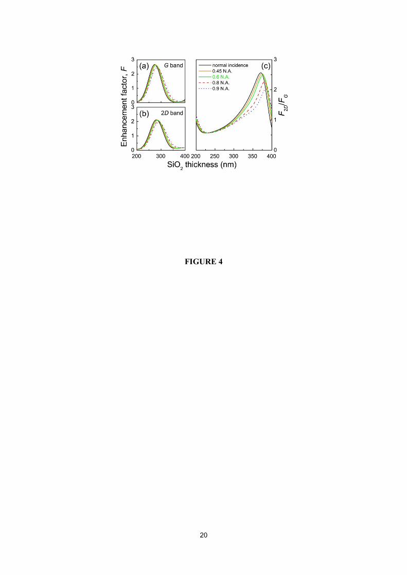
In general, the interference effect is a function of the incident angle of the light. In our
analysis, we assumed normal incidence because most micro Raman scattering measurements
are performed in backscattering geometry. Even when the numerical aperture (N.A.) of the
objective lens is large, the laser beam is almost normally incident on the sample provided that
the beam is Gaussian and the focused laser beam hits the sample surface at the beam waist.
However, in practice, since the focal depth is about 1 µm for N.A.=0.6 and 500 nm , it is
conceivable that a significant portion of the beam enter the sample at an oblique angle if the
focus is only slightly off. We considered the upper bound of the effect of the large N.A. on
the interference pattern, regarding a Gaussian distribution of the incident light intensity but
treating the beam path with classical ray optics. Contributions from each portion of the beam
with an incident angle ( max0 arcsin N.A. ) were calculated separately and then
integrated over .39
As shown in Fig 4(a) and (b), the patterns of the enhancement factors of

9
the G and 2D bands shift slightly for larger N.A. values. The peak positions for 0.9 N.A. is
shifted by about 10 nm with respect to those for normal incidence. The ratio of the
enhancement factors (F2D/FG) is also slightly shifted in Fig 4(c). New fitting curves including
the effect of a large N.A. value of 0.6 are shown in Fig. 2 as dashed curves. These new fitting
curves give Ii,2D/ Ii,G=3.5.
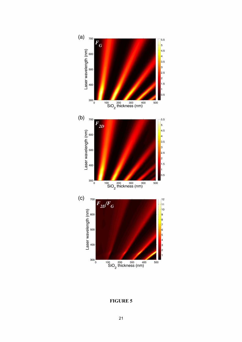
We also calculated the enhancement factors of the G (FG) and 2D (F2D) bands as functions
of the thickness of SiO2 layer and the wavelength of the excitation source for normal
incidence. The results are shown in Fig. 5(a) and (b). In this calculation, G is fixed since it
does not vary with the laser wavelength. However, the frequency of the Raman 2D band (
2 D ) depends on the laser wavelength,37
and the dispersion of the Raman 2D band can be
given as a linear function, 1
2 2444.24 99.06 cmD LaserE , where LaserE is the laser energy
in eV.38
Figures 5(a) and (b) clearly show that the Raman signal is significantly enhanced or
suppressed, depending on the laser wavelength and the SiO2 layer thickness. Figure 5(c) is a
contour plot of the ratio of the enhancement factors for the Raman 2D band to the G band. It
is clear that these factors play a major role in determining the intensity ratio. Our calculation
indicate that it is important to factor out the interference effect first, when comparing I2D/IG
data from samples with different SiO2 layer thicknesses, or obtained with different lasers. It
should also be noted that this kind of interference effect is not unique to Raman
measurements but applies to any spectroscopic measurements on thin samples on dielectric
layers. Appropriate choice of the dielectric layer thickness therefore can significantly enhance
the measured signal in such cases.
IV. SUMMARY
In summary, a strong dependence of the Raman spectrum of single layer graphene on the
10
thickness of the SiO2 layer on the substrate is observed and analyzed in terms of multiple
reflection interference. It is found that the Raman spectrum depends not only on the SiO2
layer thickness but also on the wavelength of the excitation laser. This effect significantly
influences the observed intensity ratio of the Raman 2D band to the G band.
ACKNOWLEDGMENT
This research was supported by Basic Science Research Program through the National
Research Foundation of Korea (NRF) funded by the Ministry of Education, Science and
Technology (MEST) (R01-2008-000-10685-0 and KRF-2008-314-C00111). D. Y. was
supported by the Seoul Science Fellowship. Y.-W. S. was supported in part by the NRF grant
funded by MEST (Quantum Metamaterials Research Center, R11-2008-053-01002-0 and
Nano R&D program 2008-03670). B.H.P. was partly supported by WCU program through
the NRF funded by MEST (R31-2008-000-10057-0). The work at KHU was supported by the
National Research Laboratory Fund through Nano Optical Property Laboratory.
11
REFERENCE
[1] K. S. Novoselov, A. K. Geim, S. V. Morozov, D. Jiang, Y. Zhang, S. V. Dubonos, I. V.
Grigorieva, and A. A. Firsov, Science 306, 666 (2004).
[2] K. S. Novoselov, A. K. Geim, S. V. Morozov, D. Jiang, Y. Zhang, S. V. Dubonos, I. V.
Grigorieva, and A. A. Firsov, Phys. Rev. Lett. 100, 016602 (2008).
[3] K. I. Bolotin, K. J. Sikes, J. Hone, H. L. Stormer, and P. Kim, Phys. Rev. Lett. 101,
096802 (2008).
[4] K. S. Novoselov, A. K. Geim, , S. V. Morozov, D. Jiang, M. I. Katsnelson, I. V. Grigorieva,
S. V. Dubonos, and A. A. Firsov, Nature 438, 197 (2005).
[5] Y. Zhang, Y.-W. Tan, H. L. Stormer, and P. Kim, Nature 438, 201 (2005).
[6] A. C. Ferrari, J. C. Meyer, V. Scardaci, C. Casiraghi, M. Lazzeri, F. Mauri, S. Piscanec, D.
Jiang, K. S. Novoselov, S. Roth, and A. K. Geim, Phys. Rev. Lett. 97, 187401 (2006).
[7] E. W. Hill1, A. K. Geim, K. S. Novoselov, F. Schedin, and P. Blake, IEEE Trans. Magn.
42, 2694 (2006).
[8] Z. Q. Li, E. A. Henriksen, Z. Jiang, Z. Hao, M. C. Martin, P. Kim, H. L. Stormer, and D.
N. Basov, Nature Phys. 4, 532 (2008).
[9] A. Boswick, T. Ohta, T. Seyller, K. Horn, and E. Rotenberg, Nature Phys. 3, 36 (2007).
[10] P. Mallet, F. Varchon, C. Naud, L. Magaud, C. Berger, and J.-Y. Veuillen, Phys. Rev. B
76, 041403(R) (2007).
[11] G. M. Rutter, J. N. Crain, N. P. Guisinger, T. Li, P. N. First, and J. A. Stroscio, Science
317, 219 (2007).
[12] A. Gupta, G. Chen, P. Joshi, S. Tadigadapa, and P.C. Eklund, Nano Lett. 6, 2667 (2006).

12
[13] D. Graf, F. Molitor, K. Ensslin, C. Stampfer, A. Jungen, C. Hierold, and L. Wirtz, Nano
Lett. 7, 238 (2007).
[14] D. Yoon, H. Moon, H. Cheong, J. S. Choi, J. A. Choi, and B. H. Park, J. Korean Phys.
Soc. (to be published September 2009).
[15] C. Thomsen and S. Reich, Phys. Rev. Lett. 85, 5214 (2000).
[16] J. Yan, Y. Zhang, P. Kim, and A. Pinczuk, Phys. Rev. Lett. 98, 166802 (2007).
[17] S. Pissana, M. Lazzeri, C. Casiraghi, K. S. Novoselov, A. K. Geim, A. C. Ferrari, and F.
Mauri, Nature Mater. 6, 198 (2007).
[18] A. Das, S. Pisana, B. Chakraborty, S. Piscanec. S. K. Saha, U. V. Waghmare, K. S.
Novoselov, H. R. Krishnamurthy, A. K. Geim, A. C. Ferrari, and A. K. Sood, Nature
Nanotech. 3, 210 (2008).
[19] C. Casiraghi, S. Pisana, K. S. Novoselov, A. K. Geim, and A. C. Ferrari, Appl. Phys. Lett.
91, 233108 (2007).
[20] C. Stampfer, F. Molitor, D. Graf, K. Ensslin, A. Jungen, C. Hierold, and L. Wirtz, Appl.
Phys. Lett. 91, 241907 (2007).
[21] S. Berciaud, S. Ryu, L. E. Brus, and T. F. Heinz, Nano Lett. 9, 346 (2009).
[22] D. Yoon, H. Moon, Y.-W. Son, G. Samsonidze, B. H. Park, J. B. Kim, Y. Lee, and H.
Cheong, Nano Lett. 8, 4270 (2008).
[23] F. Tuinstra and J. Koenig, J. Chem. Phys. 53, 1126 (1970).
[24] D. E. Aspnes and A. A. Studna, Phys. Rev. B 27, 985 (1983).
[25] J. J. Yoon, T. H. Ghong, J. S. Byun, Y. D. Kim, D. E. Aspenes, H. J. Kim, Y. C. Chang,
and J. D. Song, Appl. Phys. Lett. 92, 151907 (2008).
[26] The extracted refractive indices ( 2n ) of SiO2 at the wavelengths of the laser used (514.5
nm), the G band and the 2D band are 1.4643, 1.4620 and 1.4606, respectively, and those
for Si are 4.2194-0.03174i, 4.0446-0.02365i and 3.9468-0.01857i, respectively. The
13
refractive indices of graphene ( 1n ) are taken to be the same as those of graphite (2.66-
1.33i, 2.68-1.36i and 2.70-1.39i for laser, G band, 2D band, respectively) from A. Borghesi
and G. Guizzetti, “Graphite(C)” from Handbook of Optical Constants of Solids II, edited
by E. D. Palik, Academic, New York, 1991.
[27] P. Blake, E. W. Hill, A. H. Castro Neto, K. S. Novoselov, D. Jiang, R. Yang, T. J. Booth,
and A. K. Geim, Appl. Phys. Lett. 91, 063124 (2007).
[28] S. Roddaro, P. Pingue, V. Piazza, V. Pellegrini, and F. Beltram, Nano Lett. 7, 2707
(2007).
[29] I. Jung, M. Pelton, R. Piner, D. A. Dikin, S. Stankovich, S. Watcharotone, M. Hausner,
and R. S. Ruoff, Nano Lett. 7, 3569 (2007).
[30] L. Gao, W. Ren, F. Li, and H. Cheng, ACS Nano 2, 1625 (2008).
[31] Y. Y. Wang, Z. H. Ni, and Z. X. Shena, H. M. Wang, and Y. H. Wu, Appl. Phys. Lett. 92,
043121 (2008).
[32] R. J. Nemanich, C. C. Tsai, and G. A. N Connell, Phys. Rev. Lett. 44, 273 (1980).
[33] J. W. Anger III, D. K. Veirs, and G. M. Rosenblatt, J. Chem. Phys. 92, 2067 (1990).
[34] G. Chen, Jian Wu, Qiujie Lu, H. R. Gutierrez, Qihua Xiong, M. E. Pellen, J. S. Petko, D.
H. Werner, and P. C. Eklund, Nano Lett. 8, 1341 (2008).
[35] J. R. Reitz, F. J. Milford, R. W. Christy, Foundations of Electromagnetic theory, 4th ed.,
Addison-Wesley Publishing Company, USA, 1993.
[36] E. Stolyarova, K. T. Rim, S. Ryu, J. Maultzsch, P. Kim, L. E. Brus, T. F. Heinz, M. S.
Hybertsen, and G. W. Flynn, Proc. Natl. Acad. Sci. USA 104, 9209 (2007).
[37] R. P. Vidano, D. B. Fischbach, L. J. Willis, and T. M. Loehr, Sol. Stat. Comm. 39, 341
(1981).
[38] J.-C. Charlier, P.C. Eklund, J. Zhu, and A.C. Ferrari, “Electron and Phonon Properties of
Graphene: Their Relationship with Carbon Nanotubes,” from Carbon Nanotubes:
14
Advanced Topics in the Synthesis, Structure, Properties and Applications, Ed. By A. Jorio,
G. Dresselhaus, and M.S. Dresselhaus, Berlin/Heidelberg: Springer-Verlag, 2008.
15
CAPTIONS
FIG. 1. (Color online) Raman spectrum of a single layer graphene sample taken with a 514.5-
nm laser as the excitation source. Insets (a) and (b) are the optical microscope images of a
single layer graphene sample on a 350-nm SiO2 layer with white and red (filtered, 615-730
nm) light illumination, respectively. The graphene layer can be easily seen in (b), but not in
(a).
FIG. 2. (Color online) (a) G (circle dots) and 2D (square dots) band Raman intensities as
functions of the thickness of the SiO2 layer. (b) Raman intensity ratio I2D/IG as a function of
the thickness of the SiO2 layer. The stars represent data taken from Raman spectra which
showed the D band (~1350 cm-1
), and the open circles represent data taken from the samples
with high doping. The curves in (a) and (b) are the calculation results based on the MRM
model. The inset is the calculated result for 0 to 500 nm. The dashed curves are the results
when the effect of the large N.A. is included for N.A.=0.6.
FIG. 3. (Color online) Schematic diagrams of multiple reflection interference in the (a)
absorption and (b) scattering processes. 0n , 1n , 2n and 3n are the refractive indices of air,
graphene, SiO2, and Si, respectively. gd and 2SiOd are the thickness of graphene and SiO2
layer, respectively, and x is the depth in the graphene layer. The dots are the points of
interaction between the laser beam and the -electrons of graphene. (c) Calculated Raman
intensities as a function of the thickness of the SiO2 layer. The solid curve was obtained in a
simple approximation where the Raman bands and the laser are taken to have the same
wavelength.

16
FIG. 4. (Color online) Calculated Raman enhancement factors of (a) G band and (b) 2D band
as functions of the thickness of the SiO2 layer for various values of the numerical aperture of
the objective lens. The excitation wavelength is taken to be 514.5 nm. (c) Ratio of the
enhancement factor for the 2D band to that of the G band, F2D/FG.
FIG. 5. (Color online) Plots of calculated Raman enhancement factors of (a) G band and (b)
2D band as functions of the thickness of SiO2 layer and the wavelength of the laser. (c) Ratio
of the enhancement factor for the 2D band to that of the G band, F2D/FG.
17
FIGURE 1
18
FIGURE 2

19
FIGURE 3
20
FIGURE 4
21
FIGURE 5