Statistical model on the optical properties of silicon nanowire mats
10
PHYSICAL REVIEW B 84, 125432 (2011) Statistical model on the optical properties of silicon nanowire mats Gerald Br¨ onstrup * Max Planck Institute for the Science of Light, D-91058 Erlangen, Germany Frank Garwe, Andrea Cs´ aki, and Wolfgang Fritzsche Institute of Photonic Technology Jena, D-07745 Jena, Germany Andrea Steinbr¨ uck Materials Physics & Applications, Los Alamos National Laboratory, Center for Integrated Nanotechnologies, Los Alamos, New Mexico 87545, USA Silke Christiansen † Max Planck Institute for the Science of Light, D-91058 Erlangen, Germany (Received 15 April 2011; revised manuscript received 22 July 2011; published 15 September 2011) Randomly grown silicon nanowire (SiNW) mats show a high light absorption even for long wavelengths despite the small volume of silicon. We present a statistical model that gives a physical understanding of the mechanisms of the absorption and scattering of light in such SiNW mats. According to this model the two main mechanisms of the effective absorption of light are (i) resonant optical antenna effects of the absorption within the individual SiNWs and (ii) the interaction of the light with several SiNWs in the mat due to strong light scattering. The results of this model are in good agreement with the experimental reflection, transmission, and absorption spectra taken with an integrating sphere. DOI: 10.1103/PhysRevB.84.125432 PACS number(s): 78.20.Bh, 78.67.Uh, 42.25.Fx, 05.40.Fb I. INTRODUCTION Silicon nanowires (SiNWs) have attracted much atten- tion as building blocks for solar cells, 1–6 sensors, 7 and photodetectors. 8–10 A promising approach to build cost- efficient SiNW based devices is to grow mats of them that form randomly oriented on low-cost amorphous substrates like glass when relying on the so-called vapor-liquid-solid (VLS) growth mechanism. 11 In favor of this idea is that it has been shown that these SiNW mats absorb light of the whole solar spectrum efficiently. 12 However, to optimize these mats for optoelectronic applications a profound understanding of how the microstructure given by figures like SiNW radii, their lengths, and the density influences the optical properties is required. The proper description of the optical properties of such disordered SiNW mats is difficult for different reasons. Numerical simulations are usually limited to highly ordered arrays of SiNWs, 13,14 or mats consisting of relatively short NWs. 15 The randomness of the mats grown on amorphous substrates and the large ratio of the radii to the length of the SiNWs makes them entirely impossible for numerical simulations. The properties of silicon strongly depend on the wavelengths. For wavelengths shorter than ∼365 nm silicon has a direct gap 16 with a high absorption coefficient while for longer wavelengths it has an indirect band gap with a low absorption coefficient. Furthermore, it can be tedious to extract the important effects and the dependence of optical properties on different parameters from numerical simulations. Mats of direct band-gap semiconducting nanowires (NWs) have been successfully modeled with layer stacks in which each layer has an effective refractive index. 17 These NWs were only a few microns long and grew perpendicular on the substrates. To describe the interaction of mats of randomly grown SiNWs with light for the whole visible spectrum an elegant analytical model has been published by Street et al. 18 In this model the interaction of SiNW mats is described with a statistical approach combined with a Rayleigh-type model to account for the interaction of the individual SiNWs with light. When optical spectra of disordered NW mats are fitted to this model it gives basic information about values like the product of the expected value N 0 of interactions with the SiNWs and the absorption length for each NW d NW , i.e., the effective optical path length N 0 d NW . However, due to the Rayleigh-type model, resonant optical antenna effects are not taken into account and thus the influence of the microstructure, like the radii of the individual SiNWs, cannot directly be predicted. Furthermore, it has been shown that the interaction of light with individual SiNWs can be explained with the more complex Mie theory. 19 The latter reproduces the measured spectra of individual NWs very well, including the strong resonant optical antenna effects. 20–22 These resonances are strongly dependent on the radius of such NWs and to a lesser extent on the angle between the incident light and the NW. Thus at least Mie theory like models have to be used to reveal information on the influence of the microstructure. In this paper we present experimental reflection, transmis- sion, and absorption data of SiNW mats grown randomly on glass substrates for visible light, i.e., for wavelengths 320 nm λ 820 nm, taken with an integrating sphere. The spectra of the SiNW mats are explained with a statistical model, which is based on a random-walk approach (RW) 23 and Mie theory. 19 Due to the RW approach the statistical distribution of the photon paths is naturally taken into account and many other physical properties can easily be calculated. Since the Mie theory describes radius dependent properties 125432-1 1098-0121/2011/84(12)/125432(10) ©2011 American Physical Society
Transcript of Statistical model on the optical properties of silicon nanowire mats
PHYSICAL REVIEW B 84, 125432 (2011)
Statistical model on the optical properties of silicon nanowire mats
Gerald Bronstrup*
Max Planck Institute for the Science of Light, D-91058 Erlangen, Germany
Frank Garwe, Andrea Csaki, and Wolfgang FritzscheInstitute of Photonic Technology Jena, D-07745 Jena, Germany
Andrea SteinbruckMaterials Physics & Applications, Los Alamos National Laboratory, Center for Integrated Nanotechnologies, Los Alamos,
New Mexico 87545, USA
Silke Christiansen†
Max Planck Institute for the Science of Light, D-91058 Erlangen, Germany(Received 15 April 2011; revised manuscript received 22 July 2011; published 15 September 2011)
Randomly grown silicon nanowire (SiNW) mats show a high light absorption even for long wavelengthsdespite the small volume of silicon. We present a statistical model that gives a physical understanding of themechanisms of the absorption and scattering of light in such SiNW mats. According to this model the two mainmechanisms of the effective absorption of light are (i) resonant optical antenna effects of the absorption withinthe individual SiNWs and (ii) the interaction of the light with several SiNWs in the mat due to strong lightscattering. The results of this model are in good agreement with the experimental reflection, transmission, andabsorption spectra taken with an integrating sphere.
DOI: 10.1103/PhysRevB.84.125432 PACS number(s): 78.20.Bh, 78.67.Uh, 42.25.Fx, 05.40.Fb
I. INTRODUCTION
Silicon nanowires (SiNWs) have attracted much atten-tion as building blocks for solar cells,1–6 sensors,7 andphotodetectors.8–10 A promising approach to build cost-efficient SiNW based devices is to grow mats of them thatform randomly oriented on low-cost amorphous substrateslike glass when relying on the so-called vapor-liquid-solid(VLS) growth mechanism.11 In favor of this idea is that it hasbeen shown that these SiNW mats absorb light of the wholesolar spectrum efficiently.12 However, to optimize these matsfor optoelectronic applications a profound understanding ofhow the microstructure given by figures like SiNW radii, theirlengths, and the density influences the optical properties isrequired.
The proper description of the optical properties of suchdisordered SiNW mats is difficult for different reasons.Numerical simulations are usually limited to highly orderedarrays of SiNWs,13,14 or mats consisting of relatively shortNWs.15 The randomness of the mats grown on amorphoussubstrates and the large ratio of the radii to the length ofthe SiNWs makes them entirely impossible for numericalsimulations. The properties of silicon strongly depend on thewavelengths. For wavelengths shorter than ∼365 nm siliconhas a direct gap16 with a high absorption coefficient whilefor longer wavelengths it has an indirect band gap with a lowabsorption coefficient. Furthermore, it can be tedious to extractthe important effects and the dependence of optical propertieson different parameters from numerical simulations. Mats ofdirect band-gap semiconducting nanowires (NWs) have beensuccessfully modeled with layer stacks in which each layerhas an effective refractive index.17 These NWs were only afew microns long and grew perpendicular on the substrates.To describe the interaction of mats of randomly grown SiNWs
with light for the whole visible spectrum an elegant analyticalmodel has been published by Street et al.18 In this modelthe interaction of SiNW mats is described with a statisticalapproach combined with a Rayleigh-type model to accountfor the interaction of the individual SiNWs with light. Whenoptical spectra of disordered NW mats are fitted to this modelit gives basic information about values like the product of theexpected value N0 of interactions with the SiNWs and theabsorption length for each NW dNW , i.e., the effective opticalpath length N0dNW .
However, due to the Rayleigh-type model, resonant opticalantenna effects are not taken into account and thus the influenceof the microstructure, like the radii of the individual SiNWs,cannot directly be predicted. Furthermore, it has been shownthat the interaction of light with individual SiNWs can beexplained with the more complex Mie theory.19 The latterreproduces the measured spectra of individual NWs verywell, including the strong resonant optical antenna effects.20–22
These resonances are strongly dependent on the radius ofsuch NWs and to a lesser extent on the angle between theincident light and the NW. Thus at least Mie theory like modelshave to be used to reveal information on the influence of themicrostructure.
In this paper we present experimental reflection, transmis-sion, and absorption data of SiNW mats grown randomlyon glass substrates for visible light, i.e., for wavelengths320 nm � λ � 820 nm, taken with an integrating sphere. Thespectra of the SiNW mats are explained with a statisticalmodel, which is based on a random-walk approach (RW)23
and Mie theory.19 Due to the RW approach the statisticaldistribution of the photon paths is naturally taken into accountand many other physical properties can easily be calculated.Since the Mie theory describes radius dependent properties
125432-11098-0121/2011/84(12)/125432(10) ©2011 American Physical Society
GERALD BRONSTRUP et al. PHYSICAL REVIEW B 84, 125432 (2011)
of the individual SiNWs it is possible to predict the effect ofthe microstructure of the mat on its optical properties. It iseven possible to predict the influence of layers of transparentconductive oxides (TCO), which can be used to electricallycontact future SiNW based devices, simply by using theappropriate values for the scattering and absorption crosssections of the individual NWs. With this model it is possibleto fit the experimental transmission, reflection, and absorptionspectra simultaneously with only three parameters, in spite ofthe complex structure of the mats. All of the parameters havea direct physical meaning: One is related to the length and thedensity of the SiNWs and two describe the radii distributionof the SiNWs in the mats.
II. MODEL
The model to describe the optical properties of disorderedSiNW mats is based on the assumption that their interactionwith light can be split in two different phenomena: (i) The firstphenomenon describes the interaction of light with individualSiNWs, and (ii) the second phenomenon describes how theoptical properties of individual SiNWs influence the opticalproperties of ensembles of many SiNWs, i.e., the disorderedSiNW mats. In this paper, the first phenomenon will be referredto as the ‘antenna problem’ and the second as the “macroscopicproblem.” Finally, the interaction of the light with the SiNWgrowth substrate has to be taken into account.
The name “antenna problem” has been chosen, because thisproblem will be tackled using Mie theory. Though, strictlyspeaking, these Mie resonances do not describe the classicalantenna phenomenon, they have been labeled as “optical an-tenna effects” when they occur with semiconducting NWs.20,24
To solve the “macroscopic problem” many approacheshave been published. The typical mean free path length l ofthe respective system is one criterion to chose an appropriateapproximation. Two types of mean free paths have to bedistinguished, the mean free scattering path length lsca and themean free extinction path length lext. The first one describes thetypical distance that a photon can travel before it is scattered,the latter one describes the typical distance before it is extinct,i.e., scattered or absorbed. Three regimes can roughly bedistinguished by the mean free path:25 First, the propagationof light can be modeled as a diffusion or with RWs26,27 onlength scales much larger than the mean free path, the so calledmacroscopic regime. RWs are, however, more accurate whenthe mean path length of the photons is low.28 These approxi-mations completely neglect all interference effects. Second, iflength scales comparable to the mean free path are importantthe regime is called mesoscopic. A well-known mesoscopicphenomenon is the enhanced backscattering cone, which isrelated to constructive interference of inverse paths of thelight in the scattering medium. The analyses of the enhancedbackscattering cone has been successfully employed for GaPNW mats.29 However, this effect occurs only for systems withnon negligible absorption. Since non negligible absorptionoccurs in the SiNWs, which are examined in this work, thiseffect can be ignored. Third, on small length scales, i.e., themicroscopic regime, the Maxwell equations have to be solved.
Here we chose a RW model. These kind of models are oftenbased on the optical properties of individual particles that are
well separated, i.e., independent scattering of particles.26,30
Therefore they cannot account for interference effects, relatedto many particles, and thus it does not include how neighboringparticles change the scattering and extinction properties of thisparticle. If the optical properties of the individual particlesare changed by the surrounding particles the effect is calleddependent scattering. The latter becomes dominant for26
2πlext
λ� 2Csca
Cext. (1)
Here Csca is the scattering cross section of the particlesand Cext is the extinction cross section. Though the typicallext for the SiNW mats are not yet known, it will be shown inhindsight that dependent scattering is not dominant. Taking thisinto consideration, the RW approach could be an appropriateapproximation. If these models are a good approximation theyhave several advantages.
RW models have proven to give good results and relativelysimple equations.23 Furthermore, they can deliver a lot ofadditional information.23,27 The RW models assume that thephotons are scattered in some kind of discrete lattice and thateach interaction event is independent of the prior path of thephoton. At each lattice point the photon is either scatteredto one of the neighboring points of the lattice or absorbedwith a given probability. For a given starting point of thephoton it is in principle possible to calculate the possibilities ofevery possible path of the photon in the lattice. Transferred toexperimental data this would mean that it is possible to predicthow the intensity of the light is three dimensionally distributedin the scattering medium, including where it is scattered outof the SiNW mat and where it is absorbed.
We employ the RW model for “optically turbid slabs”as published in Ref. 23, which was originally designed todescribe the interaction of light with biological tissue. Thoughthe model has been developed for a completely differentmaterial it is applicable to the SiNW mats, since no specialassumptions have been made that restrict the model to biologictissue. This model provides for analytical equations for thediffuse reflection, transmission, and absorption of such SiNWmats, when the effective scattering cross sections Ceff
sca andabsorption cross sections Ceff
abs of the SiNWs are known. Thedetermination of appropriate cross sections is referred to asthe antenna problem and is described later in this paper.This RW model uses a three-dimensional RW on an isotropicrectangular scattering lattice. At each lattice point the photonsare either absorbed or scattered to a neighboring lattice point.The probability of which neighboring lattice point a scatteredphoton migrates to is equally distributed between the sixpossible neighbors. When a photon is scattered out of the latticeit is either reflected or transmitted. The RW scattering lattice isinfinitively long in two directions while it has a finite depth of L
lattice spacings. Thus L is a natural number and determines thethickness of the scattering lattice. The number of lattice pointsis of course not real but a natural number, or, to be more precise,a denumerably infinite number, since the lattice is assumed tobe infinitely extended in two directions. The not real numberof lattice points in the final formulas is only visible in thethickness of the mat L, which, however, can easily be replacedby a real variable as long as L � 1. A value of 0 < L < 1corresponds to less than one lattice layer of the RW lattice and
125432-2
STATISTICAL MODEL ON THE OPTICAL PROPERTIES . . . PHYSICAL REVIEW B 84, 125432 (2011)
has to be taken into special consideration. For a real slab thethickness of the mat L is related to the sum of the scatteringcross sections of all scatterers in a volume with the heightof the mat and a unit face area. When an effective scatteringcross section Ceff
sca is assumed L is consequently connectedto the product of the number of scatterers in such a volumewith a unit face area and their scattering cross sections, i.e., alarger number of scatterers or larger scattering cross sectionscorrespond to a larger number L of lattice layers. Since thescattering cross sections are dependent on the wavelength λ
the appropriate value for L is also dependent on the wavelengthλ. To take this dependence into consideration we approximateL to be proportional to the averaged effective scattering crosssections Ceff
sca of the SiNWs:
L = αCeff
sca
r. (2)
Here r is the average radius of the SiNWs in the mat and α
is a scaling constant. Like the values for the cross sectionsobtained by Mie theory for cylinders, the dimension of theeffective scattering cross sections Ceff
sca will have the dimensionof a length19 and not as usual an area, since infinitively long
cylinders are assumed. Thus the fraction Ceffscar
is dimensionless,as is the number L of scattering lattice layers. Accordingly, thescaling constant α is also dimensionless. Since the wavelengthdependence of L is now reduced to the wavelength dependenceof Ceff
sca the scaling constant α is really a constant and notdependent on the wavelength λ. It should be proportional tothe number of scatterers in a volume with a unit face area. Forthe SiNW mats this implies that it is proportional to the lengthand the density of the SiNWs in the mat.
Since the entire photon path distribution can be calculatedwithin this model it opens the way to predict other opticalproperties of such SiNW mats, e.g., how much light is absorbedin which depth of the mat or the radial distribution of there-emitted light. Optical properties of SiNW mats such as thediffuse reflection and transmission can easily experimentallybe determined. These values are given by the proposed modelin dependence of the ratio μ of the effective absorption Ceff
absand scattering cross section Ceff
sca and the thickness L of theSiNW mat. For L � 1 the reflection Rmat and the transmissionTmat of the mat are given by23
μ = Ceffabs/Ceff
sca, (3)
Rmat(μ,L � 1) = e−2μ
√24μ
[1 − e
√24μ + 2
1 − cosh√
24μ
eL√
24μ − 1
],
(4)
Tmat(μ,L � 1) = e−2μ
√24μ
[cosh
√24μ − 1
sinh L√
6μ
]. (5)
In this work values of the reflection Rmat and the transmissionTmat of the mat for values of the thickness L with 0 < L < 1have been approximated by a linear scaling:
Rmat(μ,0 < L < 1) = LRmat(μ,L = 1), (6)
Tmat(μ,0 < L < 1) = (1 − L) + LTmat(μ,L = 1). (7)
Since the values for the reflection Rmat(μ,L) and the transmis-sion Tmat(μ,L) of the SiNW mats include the diffuse scatteredlight, the absorption of the mat Amat(μ,L) is given by
Amat(μ,L) = 1 − Rmat(μ,L) − Tmat(μ,L). (8)
The scattering mean free path lsca is also readily available.Since the distance between the scattering layers is equal tothis mean free scattering path lsca,28 it can be calculated, whenthe real thickness of the mat t is known and the number ofscattering layers L:
lsca = t/L. (9)
A more common value is the extinction mean free path,which is also easy to calculate, within the approximations ofthis model. The scattering mean free path lsca is also related tothe particle density ndensity, by lsca = 1/(ndensity Csca).31 A sim-ilar expression is found for the extinction mean free path lext =1/ndensity Cext. Cext = Csca + Cabs is the extinction cross sec-tion. Thus the extinction mean free path is given by lext = llsca
Csca/Cext = lsca/(1 + Cabs/Csca) ⇒
lext = llsca
1 + μ. (10)
Due to this RW model [Eqs. (3)–(8)] it is sufficient tofind some expressions for Ceff
abs and Ceffsca to solve the antenna
problem. For individual SiNWs the cross sections Cabs andCsca can easily be calculated using Mie theory19 and theirproperties have been investigated in great detail.20–22
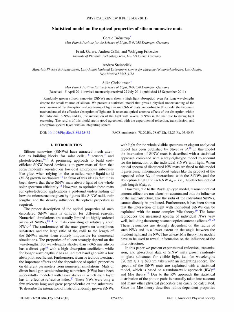
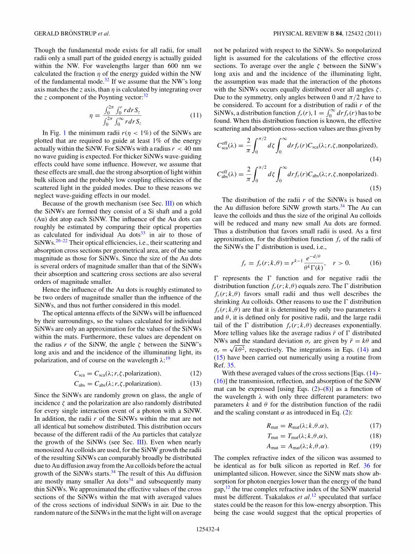
At this point it has to be stressed that potential waveguideeffects are not included in the RW model. This can be donefor several reasons. The first reason is the small mean freepath of light in bulk silicon, which can be calculated fromthe complex refractive index n by λ/[4π �(n)]. It is plottedin Fig. 1. For wavelengths smaller than ∼650 nm it is smallerthan the wavelength itself. Thus wave guiding can only havean effect for large wavelengths. Second, guided modes need tobe excited by the incident light; this will preferably happen atsome distortions near the SiNWs and thus it is hard to estimatereasonable value. Finally, only the thickest NWs in our matswould be able to efficiently guide even the fundamental mode.
FIG. 1. (Color online) The mean free path of light in bulk silicon(left axis) and the minimum radii r(η < 1%) of the SiNWs are plottedthat are required to guide at least 1% of the energy of the fundamentalmode within the SiNW. The calculations have been done followingRef. 32, using only the real part of the refractive index of silicon.
125432-3
GERALD BRONSTRUP et al. PHYSICAL REVIEW B 84, 125432 (2011)
Though the fundamental mode exists for all radii, for smallradii only a small part of the guided energy is actually guidedwithin the NW. For wavelengths larger than 600 nm wecalculated the fraction η of the energy guided within the NWof the fundamental mode.32 If we assume that the NW’s longaxis matches the z axis, than η is calculated by integrating overthe z component of the Poynting vector:32
η =∫ 2π
0
∫ r
0 rdrSz∫ 2π
0
∫ ∞0 rdrSz
(11)
In Fig. 1 the minimum radii r(η < 1%) of the SiNWs areplotted that are required to guide at least 1% of the energyactually within the SiNW. For SiNWs with a radius r < 40 nmno wave guiding is expected. For thicker SiNWs wave-guidingeffects could have some influence. However, we assume thatthese effects are small, due the strong absorption of light withinbulk silicon and the probably low coupling efficiencies of thescattered light in the guided modes. Due to these reasons weneglect wave-guiding effects in our model.
Because of the growth mechanism (see Sec. III) on whichthe SiNWs are formed they consist of a Si shaft and a gold(Au) dot atop each SiNW. The influence of the Au dots canroughly be estimated by comparing their optical propertiesas calculated for individual Au dots33 in air to those ofSiNWs.20–22 Their optical efficiencies, i.e., their scattering andabsorption cross sections per geometrical area, are of the samemagnitude as those for SiNWs. Since the size of the Au dotsis several orders of magnitude smaller than that of the SiNWstheir absorption and scattering cross sections are also severalorders of magnitude smaller.
Hence the influence of the Au dots is roughly estimated tobe two orders of magnitude smaller than the influence of theSiNWs, and thus not further considered in this model.
The optical antenna effects of the SiNWs will be influencedby their surroundings, so the values calculated for individualSiNWs are only an approximation for the values of the SiNWswithin the mats. Furthermore, these values are dependent onthe radius r of the SiNW, the angle ζ between the SiNW’slong axis and and the incidence of the illuminating light, itspolarization, and of course on the wavelength λ:19
Csca = Csca(λ; r,ζ,polarization), (12)
Cabs = Cabs(λ; r,ζ,polarization). (13)
Since the SiNWs are randomly grown on glass, the angle ofincidence ζ and the polarization are also randomly distributedfor every single interaction event of a photon with a SiNW.In addition, the radii r of the SiNWs within the mat are notall identical but somehow distributed. This distribution occursbecause of the different radii of the Au particles that catalyzethe growth of the SiNWs (see Sec. III). Even when nearlymonosized Au colloids are used, for the SiNW growth the radiiof the resulting SiNWs can comparably broadly be distributeddue to Au diffusion away from the Au colloids before the actualgrowth of the SiNWs starts.34 The result of this Au diffusionare mostly many smaller Au dots34 and subsequently manythin SiNWs. We approximated the effective values of the crosssections of the SiNWs within the mat with averaged valuesof the cross sections of individual SiNWs in air. Due to therandom nature of the SiNWs in the mat the light will on average
not be polarized with respect to the SiNWs. So nonpolarizedlight is assumed for the calculations of the effective crosssections. To average over the angle ζ between the SiNW’slong axis and and the incidence of the illuminating light,the assumption was made that the interaction of the photonswith the SiNWs occurs equally distributed over all angles ζ .Due to the symmetry, only angles between 0 and π/2 have tobe considered. To account for a distribution of radii r of theSiNWs, a distribution function fr (r), 1 = ∫ ∞
0 drfr (r) has to befound. When this distribution function is known, the effectivescattering and absorption cross-section values are thus given by
Ceffsca(λ) = 2
π
∫ π/2
0dζ
∫ ∞
0drfr (r)Csca(λ; r,ζ,nonpolarized),
(14)
Ceffabs(λ) = 2
π
∫ π/2
0dζ
∫ ∞
0drfr (r)Cabs(λ; r,ζ,nonpolarized).
(15)
The distribution of the radii r of the SiNWs is based onthe Au diffusion before SiNW growth starts.34 The Au canleave the colloids and thus the size of the original Au colloidswill be reduced and many new small Au dots are formed.Thus a distribution that favors small radii is used. As a firstapproximation, for the distribution function fr of the radii ofthe SiNWs the � distribution is used, i.e.,
fr = fr (r; k,θ ) = rk−1 e−d/θ
θk�(k), r > 0. (16)
� represents the � function and for negative radii thedistribution function fr (r; k,θ ) equals zero. The � distributionfr (r; k,θ ) favors small radii and thus well describes theshrinking Au colloids. Other reasons to use the � distributionfr (r; k,θ ) are that it is determined by only two parameters k
and θ , it is defined only for positive radii, and the large radiitail of the � distribution fr (r; k,θ ) decreases exponentially.More telling values like the average radius r of � distributedNWs and the standard deviation σr are given by r = kθ andσr =
√kθ2, respectively. The integrations in Eqs. (14) and
(15) have been carried out numerically using a routine fromRef. 35.
With these averaged values of the cross sections [Eqs. (14)–(16)] the transmission, reflection, and absorption of the SiNWmat can be expressed [using Eqs. (2)–(8)] as a function ofthe wavelength λ with only three different parameters: twoparameters k and θ for the distribution function of the radiiand the scaling constant α as introduced in Eq. (2):
Rmat = Rmat(λ; k,θ,α), (17)
Tmat = Tmat(λ; k,θ,α), (18)
Amat = Amat(λ; k,θ,α). (19)
The complex refractive index of the silicon was assumed tobe identical as for bulk silicon as reported in Ref. 36 forunimplanted silicon. However, since the SiNW mats show ab-sorption for photon energies lower than the energy of the bandgap,12 the true complex refractive index of the SiNW materialmust be different. Tsakalakos et al.12 speculated that surfacestates could be the reason for this low-energy absorption. Thisbeing the case would suggest that the optical properties of
125432-4
STATISTICAL MODEL ON THE OPTICAL PROPERTIES . . . PHYSICAL REVIEW B 84, 125432 (2011)
SiNWs with small radii would most effectively be affected, dueto the highest surface-to-volume ratio. Another explanationcould be some kind of doping of the SiNWs. For wavelengthscorresponding to photon energies lower than the energy of theband gap of Si (λgap = 1120 nm37), the absorption coefficientis changed drastically for high doping concentrations.38 ForSiNWs grown similar to our SiNW mats, high Au dopingconcentrations have been reported.39 Unfortunately, there isno complex refractive index of Au-doped silicon published tothe best of our knowledge. Nevertheless, the influence of thedoping should be small for wavelengths much smaller than1120 nm. Due to this fact we restrict our considerations to thevisible spectrum, i.e., 320 nm < λ < 820 nm.
Finally, the substrate on which the SiNW mats are grownhas to be considered. Here we used glass substrates with noconsiderable absorption but only a certain reflection. Thereflection at the interface between the SiNW mat and thesubstrate is unknown. To roughly estimate this effect, weassumed that about half of the surface is covered with siliconand thus an effective refractive index of the mat at the interfaceof about half the value of silicon, which is about 3.5 for mostwavelengths of the visible spectrum.36 This resulted in a negli-gible reflection. Since this reflection is even further decreasedin the measured spectra, by the fact that only a fraction of lightreaches the interface, we roughly approximated the reflectivityof this interface with zero. The reflection Rsubstrate at thebackside of the substrate is roughly approximated as well. Ithas been assumed to be 4%, according to the classical valuefor a refractive index of 1.5 of the substrate. To estimate theeffect of the substrate, multiple reflections between the backside of the substrate and the SiNW mat have to be considered.This effect would enhance the reflection of the sample sincethe light, which is transmitted through the SiNW mat, canbe reflected at the back side of the substrate and can then betransmitted though the SiNW mat again. Thus the reflectionof the sample by the first reflection at the back side of thesubstrate could be increased according to Tmat Rsubstrate Tmat
and in a similar way by a second reflection at the NW matand the back side by Tmat Rsubstrate Rmat Rsubstrate Tmat and soon for multiple reflections of this type. Thus the reflection ofthe whole sample Rsample can be described by Rsample=Rmat +TmatRsubstrateTmat +TmatRsubstrateRmatRsubstrateTmat · · · = Rmat +T 2
mat Rsubstrate∑∞
n=0(Rsubstrate Rmat)n. The transmission of thewhole sample Tsample is decreased in a similar way, resultingin the following expressions for the entire sample:
Rsample = Rmat + T 2mat Rsubstrate
∞∑n=0
(Rsubstrate Rmat)n
= Rmat + T 2mat Rsubstrate
1 − Rsubstrate Rmat, (20)
Tsample = Tmat
∞∑n=0
(Rsubstrate Rmat)n
= Tmat
1 − Rsubstrate Rmat. (21)
From these formulas it can be seen that the values of thetransmission and the reflection are not strongly influenced bythe substrate, as long as the reflection of the substrate Rsubstrate
assumes not more than a few percent. Since other approxima-tions in our model result in certain inaccuracies, no efforts havebeen made to find a more accurate value for Rsubstrate. As soonas transmission and reflection are known values, the absorptionof the sample Asample can easily be calculated according to
Asample = 1 − Rsample − Tsample. (22)
These equations [Eqs. (20)–(22)] with the expressions forthe SiNW mats as described in Eqs. (17)–(19) have beenused to fit the experimental spectra. The fitting is based ona Levenberg-Marquardt algorithm taken from Ref. 35. Severaldifferent values have been used as starting values for the fitand the fits with the least-square errors have automaticallybeen selected. The fitting was carried out simultaneously forthe reflection, transmission, and absorption spectra, i.e., onevalue for each of the three parameters k, θ , and α is sufficientto describe all three fitted spectra of each sample.
III. EXPERIMENT
SiNW mats have been grown on a glass substrates (Corn-ing 7059) by a chemical vapor deposition (CVD) processfollowing the VLS mechanism11 with a home-built CVDreactor. The precursor gas silane was used in argon that wasused as carrier gas. The flow rates of both gases have beenheld constant at 4 sccm (sccm denotes cubic centimeter perminute at STP). The duration of the CVD process was 1 hand the total pressure was 2.0 mbar. To obtain SiNW matscomposed of SiNWs with different radii the SiNW growthwas catalyzed by commercially available Au colloids (BritishBiocell Int.) with nominally three different radii: 15, 30,
and 75 nm. The Au colloids were deposited onto the planarsurface using self-assembly techniques and silane chemistry.40
The growth temperature of the heater was kept constant ataround 590 ◦C. The samples were mounted about 1 mm awayfrom the heater. The side of the sample with the Au colloidswas facing the heater during the CVD process allowinglower temperatures and thus preventing a deposition of thinamorphous silicon layer in addition to the SiNW growth. Tocheck the reproducibility, two samples of each type of Aucolloids have been realized.
To analyze the optical properties of these SiNW mats thetotal reflection Rexpt, i.e., the directed and diffuse reflection,and the total transmission Texpt spectra have been measuredusing an integrating sphere (Lambda 900, Perkin Elmer).Since the diffuse transmission and reflection is included inthe measurements the absorption Aexpt can be calculated fromthese spectra:
Aexpt = 1 − Texpt − Rexpt. (23)
IV. RESULTS AND DISCUSSION
At areas were no Au colloids have been immobilizedthe samples did not change their clear, colorless, transparentappearance. Thus we assume that no layer of amorphous Sihas been deposited during the CVD process.
125432-5
GERALD BRONSTRUP et al. PHYSICAL REVIEW B 84, 125432 (2011)
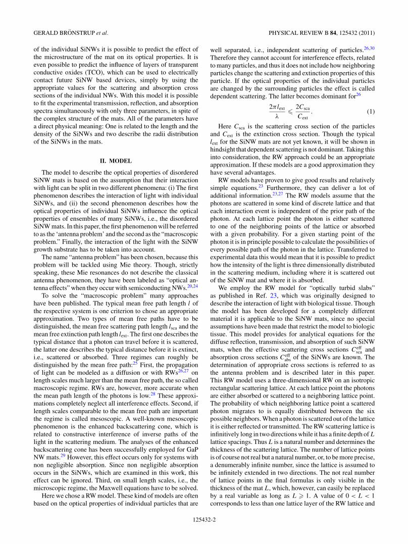
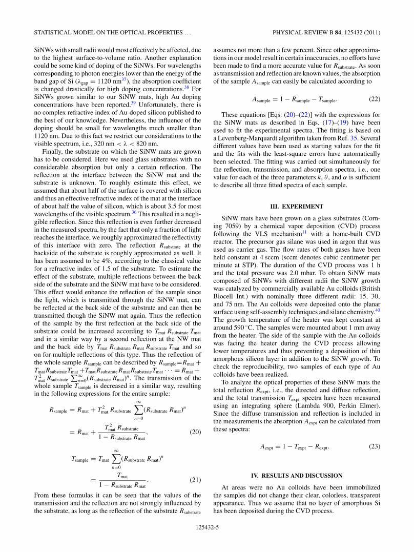
FIG. 2. SEM micrograph of SiNW mats grown using Au colloidswith 75-nm radius, tilted by 45◦. The bar represents 3 μm.
The obtained SiNW mats have been studied with scanningelectron microscopy (SEM). Dense mats have been obtained.A SEM micrograph of the sample grown with 75 nm radiusAu colloids is shown in Fig. 2. The radii of the SiNWsare broadly distributed, which is probably not due to thesharp radii of distribution of the Au colloids before thegrowth but due to the Au diffusion during the CVD processbefore the actual SiNW growth started. It is known fromliterature that Au atoms of the colloids diffuse and form verysmall particles that give rise to the growth of of very thinSiNWs.34
The thickness of the SiNW mat t has been measured fromSEM cross sections to be approximately t ≈ 30 μm.
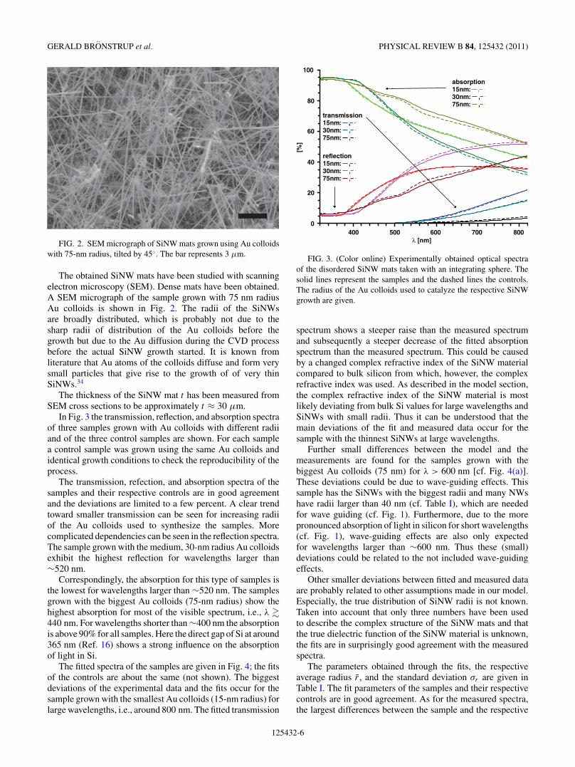
In Fig. 3 the transmission, reflection, and absorption spectraof three samples grown with Au colloids with different radiiand of the three control samples are shown. For each samplea control sample was grown using the same Au colloids andidentical growth conditions to check the reproducibility of theprocess.
The transmission, refection, and absorption spectra of thesamples and their respective controls are in good agreementand the deviations are limited to a few percent. A clear trendtoward smaller transmission can be seen for increasing radiiof the Au colloids used to synthesize the samples. Morecomplicated dependencies can be seen in the reflection spectra.The sample grown with the medium, 30-nm radius Au colloidsexhibit the highest reflection for wavelengths larger than∼520 nm.
Correspondingly, the absorption for this type of samples isthe lowest for wavelengths larger than ∼520 nm. The samplesgrown with the biggest Au colloids (75-nm radius) show thehighest absorption for most of the visible spectrum, i.e., λ �440 nm. For wavelengths shorter than ∼400 nm the absorptionis above 90% for all samples. Here the direct gap of Si at around365 nm (Ref. 16) shows a strong influence on the absorptionof light in Si.
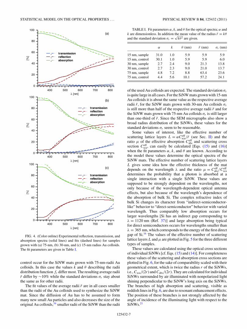
The fitted spectra of the samples are given in Fig. 4; the fitsof the controls are about the same (not shown). The biggestdeviations of the experimental data and the fits occur for thesample grown with the smallest Au colloids (15-nm radius) forlarge wavelengths, i.e., around 800 nm. The fitted transmission
[%]
0
20
40
60
80
100
λ [nm]400 500 600 700 800
transmission 15nm: ,30nm: ,75nm: ,
absorption15nm: ,30nm: ,75nm: ,
reflection 15nm: ,30nm: ,75nm: ,
FIG. 3. (Color online) Experimentally obtained optical spectraof the disordered SiNW mats taken with an integrating sphere. Thesolid lines represent the samples and the dashed lines the controls.The radius of the Au colloids used to catalyze the respective SiNWgrowth are given.
spectrum shows a steeper raise than the measured spectrumand subsequently a steeper decrease of the fitted absorptionspectrum than the measured spectrum. This could be causedby a changed complex refractive index of the SiNW materialcompared to bulk silicon from which, however, the complexrefractive index was used. As described in the model section,the complex refractive index of the SiNW material is mostlikely deviating from bulk Si values for large wavelengths andSiNWs with small radii. Thus it can be understood that themain deviations of the fit and measured data occur for thesample with the thinnest SiNWs at large wavelengths.
Further small differences between the model and themeasurements are found for the samples grown with thebiggest Au colloids (75 nm) for λ > 600 nm [cf. Fig. 4(a)].These deviations could be due to wave-guiding effects. Thissample has the SiNWs with the biggest radii and many NWshave radii larger than 40 nm (cf. Table I), which are neededfor wave guiding (cf. Fig. 1). Furthermore, due to the morepronounced absorption of light in silicon for short wavelengths(cf. Fig. 1), wave-guiding effects are also only expectedfor wavelengths larger than ∼600 nm. Thus these (small)deviations could be related to the not included wave-guidingeffects.
Other smaller deviations between fitted and measured dataare probably related to other assumptions made in our model.Especially, the true distribution of SiNW radii is not known.Taken into account that only three numbers have been usedto describe the complex structure of the SiNW mats and thatthe true dielectric function of the SiNW material is unknown,the fits are in surprisingly good agreement with the measuredspectra.
The parameters obtained through the fits, the respectiveaverage radius r , and the standard deviation σr are given inTable I. The fit parameters of the samples and their respectivecontrols are in good agreement. As for the measured spectra,the largest differences between the sample and the respective
125432-6
STATISTICAL MODEL ON THE OPTICAL PROPERTIES . . . PHYSICAL REVIEW B 84, 125432 (2011)
[%]
0
20
40
60
80
100
λ [nm]400 500 600 700 800
400 500 600 700 800
400 500 600 700 800
, transmission , reflection , absorption
[%]
0
20
40
60
80
100
λ [nm]
, transmission , reflection , absorption
[%]
0
20
40
60
80
100
λ [nm]
, transmission, reflection, absorption
(a)
(b)
(c)
FIG. 4. (Color online) Experimental reflection, transmission, andabsorption spectra (solid lines) and fits (dashed lines) for samplesgrown with (a) 75-nm, (b) 30-nm, and (c) 15-nm radius Au colloids.The fit parameters are given in Table I.
control occur for the SiNW mats grown with 75-nm-radii Aucolloids. In this case the values k and θ describing the radiidistribution function fr differ most. The resulting average radiir differ by ∼10% while the standard deviations σr stay aboutthe same as for other radii.
The fit values of the average radii r are in all cases smallerthan the radii of the Au colloids used to synthesize the SiNWmat. Since the diffusion of Au has to be assumed to formmany new small Au particles and also decreases the size of theoriginal Au colloids,34 smaller radii of the SiNW than the radii
TABLE I. Fit parameters α, k, and θ for the optical spectra; α andk are dimensionless. In addition the mean value of the radius r = kθ
and the standard deviation σr = √kθ2 are given.
α k θ (nm) r (nm) σr (nm)
15 nm, sample 31.0 1.0 5.9 5.9 5.915 nm, control 30.1 1.0 5.9 5.9 6.030 nm, sample 2.7 2.4 9.0 21.3 13.830 nm, control 2.7 2.3 9.0 21.0 13.775 nm, sample 4.8 7.2 8.8 63.4 23.675 nm, control 4.4 5.6 10.1 57.2 24.1
of the used Au colloids are expected. The standard deviation σr
is quite large in all cases. For the SiNW mats grown with 15-nmAu colloids it is about the same value as the respective averageradii r , for the SiNW mats grown with 30-nm Au colloids σr
is still more than half of the respective average radii r and forthe SiNW mats grown with 75-nm Au colloids σr is still largerthan one-third of r . Since the SEM micrographs also show abroad radius distribution of the SiNWs, these values for thestandard deviations σr seem to be reasonable.
Some values of interest, like the effective number ofscattering lattice layers L = αCeff
sca/r (see Sec. II) and theratio μ of the effective absorption Ceff
abs and scattering crosssection Ceff
sca, can easily be calculated [Eqs. (15) and (16)]when the fit parameters α, k, and θ are known. According tothe model these values determine the optical spectra of theSiNW mats. The effective number of scattering lattice layersL gives some idea how the effective thickness of the matdepends on the wavelength λ and the ratio μ = Ceff
abs/Ceffsca
determines the probability that a photon is absorbed at asingle interaction with a single SiNW. These values aresupposed to be strongly dependent on the wavelengths, notonly because of the wavelength-dependent optical antennaeffects, but also because of the wavelength’s dependence ofthe absorption of bulk Si. The complex refractive index ofbulk Si changes its character from “indirect-semiconductor-like” behavior to “direct-semiconductor” behavior with variedwavelength. Thus comparably low absorption occurs forlarger wavelengths [Si has an indirect gap corresponding toλ = 1120 nm (Ref. 37)] and large absorption being typicalfor direct semiconductors occurs for wavelengths smaller thanλ = 365 nm, which corresponds to the energy of the first directgap of Si.16 The values of the effective number of scatteringlattice layers L and μ are plotted in Fig. 5 for the three differenttypes of samples.
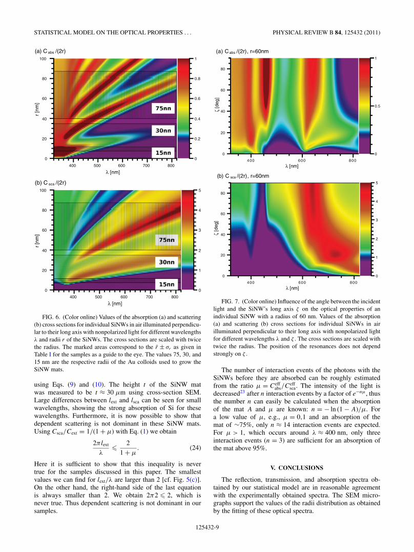
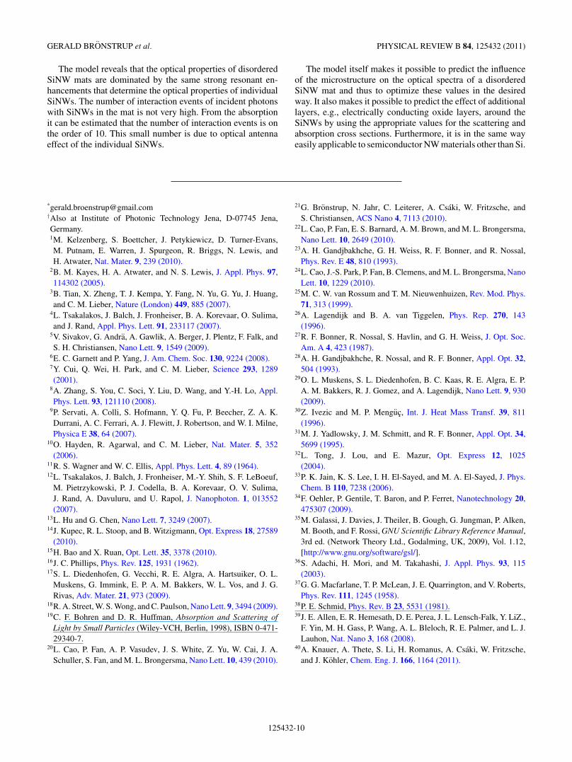
These values are calculated using the optical cross sectionsof individual SiNWs [cf. Eqs. (15) and (14)]. For completenessthese values of the scattering and absorption cross sections areplotted in Fig. 6, for the sake of comparability scaled with theirgeometrical extent, which is twice the radius r of the SiNWs,i.e., Csca/(2r) and Cabs/(2r). They are calculated for individualSiNWs surrounded by air illuminated with nonpolarized lightshining perpendicular to the SiNW’s long axis on the SiNWs.The branches of high absorption and scattering, visible asreddish lines in Fig. 6, are due to resonant enhancement effects.The position of these branches is not strongly affected by theangle of incidence of the illuminating light with respect to theSiNWs.21
125432-7

GERALD BRONSTRUP et al. PHYSICAL REVIEW B 84, 125432 (2011)
µ=C
abs
/Csc
a
0.1
1
λ [nm]400 500 600 700 800
400 500 600 700 800
400 500 600 700 800
15nm 30nm 75nm
(a) L
[-]
1
10
λ [nm]
15nm 30nm 75nm
(b)
[µm
]
0
10
20
30
λ [nm]
lext: solid linelsca: dotted
15nm 30nm 75nm
(c)
FIG. 5. (Color online) Values obtained from Mie calculationsfor the optical antenna effect in a log scale. The radii of the Aucolloids used to grow the SiNW mats are given. (a) The ratio of theeffective absorption and scattering cross section μ = Ceff
abs/Ceffsca. The
gray lines represent μ = 1,0 and μ = 0,1 as a guide for the eye.(b) The thickness of the mat L. (c) Plot of the mean free scatteringpath lsca and mean free extinction path lext on a linear scale. The fitparameters are given in Table I.
The effective number of the effective scattering latticelayers L has a local minimum around λ = 350 nm for allsamples (cf. Fig. 5). This is related to the low values ofthe scattering cross sections Csca for individual SiNWs forwavelengths shorter than ∼370 nm (cf. Fig. 6). The resonantenhancement of the effective scattering cross section Ceff
sca leadsto maxima of L at different wavelengths. The general trend isthat the maximum is shifted to larger wavelengths when theSiNWs in the mat have larger radii. For the SiNW mat with thethinnest SiNWs, grown with Au colloids with a radius of 15nm,the maximum of L is obtained at λ ≈ 420 nm and it shows asteep drop to larger wavelengths. This steep drop is becausethese SiNWs are so thin that only the first resonance attributessignificantly to the effective scattering cross sections Ceff
sca (cf.Fig. 6). The sample grown with the intermediate Au colloidswith a radius of 30 nm consists of thicker SiNWs, accordingto the fit values. Thus the first resonance of the scattering crosssection Csca of the individual SiNWs (cf. Fig. 6) is shiftedto larger wavelengths and a second resonance influences theeffective scattering cross section Ceff
sca. As a consequence, L
shows only a weak decay to larger wavelengths (cf. Fig. 6).For the SiNW mats grown with the biggest Au colloids witha radius of 75 nm the SiNWs are even thicker. For SiNWswith these radii a strong resonance covers the whole visiblespectrum and thus influences the effective scattering crosssection Ceff
sca (cf. Fig. 6). The maximum of L is not reachedfor the wavelengths discussed in this paper. Consequently, L
shows a monotonic rise for wavelengths larger than ∼380 nm.The direct gap corresponding to λ ≈ 365 nm (Ref. 16)
results in high absorption cross sections Cabs of individualSiNWs.21 Accordingly the ratio μ = Ceff
abs/Ceffsca reaches the
highest values for short wavelengths for all three samples (cf.Fig. 5).
For wavelengths larger than 400 nm μ is decreasing for allsamples. However, the slope of the decrease is significantlysmaller for the samples grown with the largest Au colloids(radius of 75 nm). These higher values of μ consequentlyresult in a higher absorption of the mat for large wavelengths(cf. Fig. 4). The reason for these high values of μ for thissample is a strong resonance, which results in high absorptioncross sections Cabs of the individual SiNWs (cf. Figs. 6 and 7).Another reason of the higher absorption of this sample is theincreasing values of the effective number of scattering latticelayers L for larger wavelengths.
When comparing the measured reflection spectra of thetwo other samples it is noticeable that for wavelengths below∼520 nm the reflection of the sample grown with the smallerAu colloids with a 15-nm radius is higher than the reflectionof the sample grown with the intermediate Au colloids witha radius of 30 nm. For larger wavelengths the opposite is true(cf. Fig. 3). Though the values of μ of these samples do notdiffer significantly, the same turning point can be found for μ
(cf. Fig. 5).For all analyzed spectra in this paper the values of μ =
Ceffabs/Ceff
sca and L are determined by only a few resonances.Since the optical spectra of the mat are determined bythese values, the optical spectra of the mats themselves aredetermined by only a few resonances.
The scattering mean free path lsca and the extinction meanfree path lext are plotted in Fig. 5(c). They have been calculated
125432-8
STATISTICAL MODEL ON THE OPTICAL PROPERTIES . . . PHYSICAL REVIEW B 84, 125432 (2011)
(a) C abs /(2r)
r [n
m]
0
20
40
60
80
100
0
0.2
0.4
0.6
0.8
1
λ [nm]400 500 600 700 800
(b) C sca /(2r)
r [n
m]
0
20
40
60
80
100
0
1
2
3
4
5
λ [nm]400 500 600 700 800
FIG. 6. (Color online) Values of the absorption (a) and scattering(b) cross sections for individual SiNWs in air illuminated perpendicu-lar to their long axis with nonpolarized light for different wavelengthsλ and radii r of the SiNWs. The cross sections are scaled with twicethe radius. The marked areas correspond to the r ± σr as given inTable I for the samples as a guide to the eye. The values 75, 30, and15 nm are the respective radii of the Au colloids used to grow theSiNW mats.
using Eqs. (9) and (10). The height t of the SiNW matwas measured to be t ≈ 30 μm using cross-section SEM.Large differences between lext and lsca can be seen for smallwavelengths, showing the strong absorption of Si for thesewavelengths. Furthermore, it is now possible to show thatdependent scattering is not dominant in these SiNW mats.Using Csca/Cext = 1/(1 + μ) with Eq. (1) we obtain
2πlext
λ� 2
1 + μ. (24)
Here it is sufficient to show that this inequality is nevertrue for the samples discussed in this paper. The smallestvalues we can find for lext/λ are larger than 2 [cf. Fig. 5(c)].On the other hand, the right-hand side of the last equationis always smaller than 2. We obtain 2π2 � 2, which isnever true. Thus dependent scattering is not dominant in oursamples.
(a) C abs /(2r), r=60nm
ζ [d
eg]
0
20
40
60
80
0
0.5
1
λ [nm]008006004
(b) C sca /(2r), r=60nm
ζ [d
eg]
0
20
40
60
80
0
1
2
3
4
5
λ [nm]008006004
FIG. 7. (Color online) Influence of the angle between the incidentlight and the SiNW’s long axis ζ on the optical properties of anindividual SiNW with a radius of 60 nm. Values of the absorption(a) and scattering (b) cross sections for individual SiNWs in airilluminated perpendicular to their long axis with nonpolarized lightfor different wavelengths λ and ζ . The cross sections are scaled withtwice the radius. The position of the resonances does not dependstrongly on ζ .
The number of interaction events of the photons with theSiNWs before they are absorbed can be roughly estimatedfrom the ratio μ = Ceff
abs/Ceffsca. The intensity of the light is
decreased23 after n interaction events by a factor of e−nμ, thusthe number n can easily be calculated when the absorptionof the mat A and μ are known: n = − ln (1 − A)/μ. Fora low value of μ, e.g., μ = 0,1 and an absorption of themat of ∼75%, only n ≈ 14 interaction events are expected.For μ > 1, which occurs around λ ≈ 400 nm, only threeinteraction events (n = 3) are sufficient for an absorption ofthe mat above 95%.
V. CONCLUSIONS
The reflection, transmission, and absorption spectra ob-tained by our statistical model are in reasonable agreementwith the experimentally obtained spectra. The SEM micro-graphs support the values of the radii distribution as obtainedby the fitting of these optical spectra.
125432-9
GERALD BRONSTRUP et al. PHYSICAL REVIEW B 84, 125432 (2011)
The model reveals that the optical properties of disorderedSiNW mats are dominated by the same strong resonant en-hancements that determine the optical properties of individualSiNWs. The number of interaction events of incident photonswith SiNWs in the mat is not very high. From the absorptionit can be estimated that the number of interaction events is onthe order of 10. This small number is due to optical antennaeffect of the individual SiNWs.
The model itself makes it possible to predict the influenceof the microstructure on the optical spectra of a disorderedSiNW mat and thus to optimize these values in the desiredway. It also makes it possible to predict the effect of additionallayers, e.g., electrically conducting oxide layers, around theSiNWs by using the appropriate values for the scattering andabsorption cross sections. Furthermore, it is in the same wayeasily applicable to semiconductor NW materials other than Si.
*[email protected]†Also at Institute of Photonic Technology Jena, D-07745 Jena,Germany.1M. Kelzenberg, S. Boettcher, J. Petykiewicz, D. Turner-Evans,M. Putnam, E. Warren, J. Spurgeon, R. Briggs, N. Lewis, andH. Atwater, Nat. Mater. 9, 239 (2010).
2B. M. Kayes, H. A. Atwater, and N. S. Lewis, J. Appl. Phys. 97,114302 (2005).
3B. Tian, X. Zheng, T. J. Kempa, Y. Fang, N. Yu, G. Yu, J. Huang,and C. M. Lieber, Nature (London) 449, 885 (2007).
4L. Tsakalakos, J. Balch, J. Fronheiser, B. A. Korevaar, O. Sulima,and J. Rand, Appl. Phys. Lett. 91, 233117 (2007).
5V. Sivakov, G. Andra, A. Gawlik, A. Berger, J. Plentz, F. Falk, andS. H. Christiansen, Nano Lett. 9, 1549 (2009).
6E. C. Garnett and P. Yang, J. Am. Chem. Soc. 130, 9224 (2008).7Y. Cui, Q. Wei, H. Park, and C. M. Lieber, Science 293, 1289(2001).
8A. Zhang, S. You, C. Soci, Y. Liu, D. Wang, and Y.-H. Lo, Appl.Phys. Lett. 93, 121110 (2008).
9P. Servati, A. Colli, S. Hofmann, Y. Q. Fu, P. Beecher, Z. A. K.Durrani, A. C. Ferrari, A. J. Flewitt, J. Robertson, and W. I. Milne,Physica E 38, 64 (2007).
10O. Hayden, R. Agarwal, and C. M. Lieber, Nat. Mater. 5, 352(2006).
11R. S. Wagner and W. C. Ellis, Appl. Phys. Lett. 4, 89 (1964).12L. Tsakalakos, J. Balch, J. Fronheiser, M.-Y. Shih, S. F. LeBoeuf,
M. Pietrzykowski, P. J. Codella, B. A. Korevaar, O. V. Sulima,J. Rand, A. Davuluru, and U. Rapol, J. Nanophoton. 1, 013552(2007).
13L. Hu and G. Chen, Nano Lett. 7, 3249 (2007).14J. Kupec, R. L. Stoop, and B. Witzigmann, Opt. Express 18, 27589
(2010).15H. Bao and X. Ruan, Opt. Lett. 35, 3378 (2010).16J. C. Phillips, Phys. Rev. 125, 1931 (1962).17S. L. Diedenhofen, G. Vecchi, R. E. Algra, A. Hartsuiker, O. L.
Muskens, G. Immink, E. P. A. M. Bakkers, W. L. Vos, and J. G.Rivas, Adv. Mater. 21, 973 (2009).
18R. A. Street, W. S. Wong, and C. Paulson, Nano Lett. 9, 3494 (2009).19C. F. Bohren and D. R. Huffman, Absorption and Scattering of
Light by Small Particles (Wiley-VCH, Berlin, 1998), ISBN 0-471-29340-7.
20L. Cao, P. Fan, A. P. Vasudev, J. S. White, Z. Yu, W. Cai, J. A.Schuller, S. Fan, and M. L. Brongersma, Nano Lett. 10, 439 (2010).
21G. Bronstrup, N. Jahr, C. Leiterer, A. Csaki, W. Fritzsche, andS. Christiansen, ACS Nano 4, 7113 (2010).
22L. Cao, P. Fan, E. S. Barnard, A. M. Brown, and M. L. Brongersma,Nano Lett. 10, 2649 (2010).
23A. H. Gandjbakhche, G. H. Weiss, R. F. Bonner, and R. Nossal,Phys. Rev. E 48, 810 (1993).
24L. Cao, J.-S. Park, P. Fan, B. Clemens, and M. L. Brongersma, NanoLett. 10, 1229 (2010).
25M. C. W. van Rossum and T. M. Nieuwenhuizen, Rev. Mod. Phys.71, 313 (1999).
26A. Lagendijk and B. A. van Tiggelen, Phys. Rep. 270, 143(1996).
27R. F. Bonner, R. Nossal, S. Havlin, and G. H. Weiss, J. Opt. Soc.Am. A 4, 423 (1987).
28A. H. Gandjbakhche, R. Nossal, and R. F. Bonner, Appl. Opt. 32,504 (1993).
29O. L. Muskens, S. L. Diedenhofen, B. C. Kaas, R. E. Algra, E. P.A. M. Bakkers, R. J. Gomez, and A. Lagendijk, Nano Lett. 9, 930(2009).
30Z. Ivezic and M. P. Menguc, Int. J. Heat Mass Transf. 39, 811(1996).
31M. J. Yadlowsky, J. M. Schmitt, and R. F. Bonner, Appl. Opt. 34,5699 (1995).
32L. Tong, J. Lou, and E. Mazur, Opt. Express 12, 1025(2004).
33P. K. Jain, K. S. Lee, I. H. El-Sayed, and M. A. El-Sayed, J. Phys.Chem. B 110, 7238 (2006).
34F. Oehler, P. Gentile, T. Baron, and P. Ferret, Nanotechnology 20,475307 (2009).
35M. Galassi, J. Davies, J. Theiler, B. Gough, G. Jungman, P. Alken,M. Booth, and F. Rossi, GNU Scientific Library Reference Manual,3rd ed. (Network Theory Ltd., Godalming, UK, 2009), Vol. 1.12,[http://www.gnu.org/software/gsl/].
36S. Adachi, H. Mori, and M. Takahashi, J. Appl. Phys. 93, 115(2003).
37G. G. Macfarlane, T. P. McLean, J. E. Quarrington, and V. Roberts,Phys. Rev. 111, 1245 (1958).
38P. E. Schmid, Phys. Rev. B 23, 5531 (1981).39J. E. Allen, E. R. Hemesath, D. E. Perea, J. L. Lensch-Falk, Y. LiZ.,
F. Yin, M. H. Gass, P. Wang, A. L. Bleloch, R. E. Palmer, and L. J.Lauhon, Nat. Nano 3, 168 (2008).
40A. Knauer, A. Thete, S. Li, H. Romanus, A. Csaki, W. Fritzsche,and J. Kohler, Chem. Eng. J. 166, 1164 (2011).
125432-10