Stable and efficient photoelectrodes for solar fuels production
334
Stable and efficient photoelectrodes for solar fuels production Carles Ros Figueras Aquesta tesi doctoral està subjecta a la llicència Reconeixement- NoComercial 4.0. Espanya de Creative Commons. Esta tesis doctoral está sujeta a la licencia Reconocimiento - NoComercial 4.0. España de Creative Commons. This doctoral thesis is licensed under the Creative Commons Attribution-NonCommercial 4.0. Spain License.
-
Upload
khangminh22 -
Category
Documents
-
view
0 -
download
0
Transcript of Stable and efficient photoelectrodes for solar fuels production
Stable and efficient photoelectrodes
for solar fuels production
Carles Ros Figueras
Aquesta tesi doctoral està subjecta a la llicència Reconeixement- NoComercial 4.0. Espanya de Creative Commons. Esta tesis doctoral está sujeta a la licencia Reconocimiento - NoComercial 4.0. España de Creative Commons. This doctoral thesis is licensed under the Creative Commons Attribution-NonCommercial 4.0. Spain License.
FACULTAT DE FÍSICA GRUP D’EMMAGATZEMATGE D’ENERGIA I SISTEMES AUTÒNOMS
PROGRAMA DE DOCTORAT EN NANOCIÈNCIES
STABLE AND EFFICIENT PHOTOELECTRODES FOR SOLAR FUELS PRODUCTION
Memòria presentada per optar al títol de doctor per la Universitat de Barcelona
Autor: CARLES ROS FIGUERAS Directors: JUAN RAMON MORANTE LLEONART
i TERESA ANDREU ARBELLA Tutor: JUAN RAMON MORANTE LLEONART
Juny 2019

"Instruïu-vos, perquè necessitarem tota la nostra intel·ligència. Emocioneu-vos, perquè necessitarem tot el nostre entusiasme.
I organitzeu-vos, perquè necessitarem tota la nostra força". Antonio Gramsci
Molins de Rei, 4 de juliol de 2019a

Index

Index C. Ros
C. Ros Index
Index
Acknowledgements ........................................................................................................... 1
List of acronyms and abbreviations ................................................................................ 5
Preface............................................................................................................................... 9
List of publications included in this thesis .................................................................... 13
Summary of results ...................................................................................................... 15
Authors’ contribution to the publications included in this thesis .................................... 19
Resum de la tesi (en Català) ......................................................................................... 23
Chapter 1 General introduction: Broader context and objectives ............................... 27 1.1 Photoelectrochemical water splitting: introduction ................................................ 29
1.2 Fundamental concepts ........................................................................................... 31
1.3 Metal oxide photoelectrodes and enhancement strategies ..................................... 37
1.4 Short band gap semiconductors for PEC water splitting ......................................... 45
1.5 Protective Layers to implement photovoltaic photoabsorbers into water splitting ... 49
1.6 Hetero junctions with the protective layer ........................................................... 69
1.7 Buried homojunctions to maximize efficiency and cell flexibility ......................... 76
1.8 Cell implementation strategies and reactors ........................................................... 81
1.9 Resume, perspective and challenges ...................................................................... 86
1.10 Scope of this research .......................................................................................... 91
Chapter 2: Enhancing metal oxide photoelectrodes performance ............................. 117
2.1 Hydrogenation and structuration of TiO2 nanorod photoanodes: doping level and the effect of illumination in trap-States filling ............................................................ 121
Chapter 3: Titanium dioxide as conductive and protective layer for silicon-based photocathodes .............................................................................................................. 141
3.1 Charge transfer characterization of ALD-grown TiO2 protective layers in silicon photocathodes ...................................................................................................... 147

Index C. Ros
Chapter 4: Adapting protective layers for thin film chalcogenide photoabsorbers ... 161
4.1 Conformal chalcopyrite based photocathode for solar refinery applications .......... 169
4.2 Turning earth abundant kesterite-based solar cells into efficient protected water-splitting photocathodes ......................................................................................... 177
Chapter 5: Conductivity and endurance of protective layers in alkaline anodic conditions. ................................................................................................................... 187
5.1 Insight into the degradation mechanisms of atomic layer deposited TiO2 as photoanode protective layer ................................................................................. 195
5.2 About degradation and regeneration mechanisms of NiO protective layers deposited by ALD on photoanodes ...................................................................................... 227
Conclusions and future work ...................................................................................... 249
Annex ........................................................................................................................... 257 A.1 Enhanced photoelectrochemical water splitting of hematite multilayer nanowire
photoanodes by tuning the surface state via bottom-up interfacial engineering ....... 265
A.2 Role of Bismuth in the Electrokinetics of Silicon Photocathodes for Solar Rechargeable Vanadium Redox Flow Batteries ..................................................... 315
A.3 Substrate-electrode (SE) interface illuminated photoelectrodes and photoelectrochemical cells .................................................................................... 327

Acknowledgements

Acknowledgements C. Ros
2

C. Ros Acknowledgements
3
When I start writing these lines one of the biggest concerns, as always, is to forget mentioning someone important on this journey. A PhD thesis is a long, exhausting and fulfilling path luckily not walked alone: friends and foes, companions and adversaries, all of them have helped me in growing as a scientist but also as a person during this period and I sincerely wanted to thank them all.
The first ones are my supervisors, to give me the opportunity to perform the PhD with them. Dra. Teresa Andreu and Prof. Juan Ramon Morante offered me the possibility to perform the PhD as a full-time job in IREC and put all the necessary resources at hand for my investigations. Also to Dr. Cristian Fábrega, to introduce me to IREC with the master thesis. They have shown me the highly interdisciplinary field of photoelectrochemistry, where intense collaboration between the chemists and physicists communities is not just welcome, but necessary, greatly opening my mind and possibilities. I hope to have contributed with my perspective in this collaborative knowledge gathering in the (not so young any more) Energy Storage and Energy Harvesting group at IREC. I would like to thank all the actual and former members of the group too for all the group meetings, congresses, discussions (scientific, or not), coffee breaks, barbecues, calçotades, room escape’s, and beers. The truth is that a PhD without that part would not be the same!
To Dra. Esther Alarcon and Prof. Albert Polman, to accept me for an international internship in the AMOLF FOM institute in Amsterdam. New knowledge, new perspectives and new friends is not enough to resume all what I learned about science and about myself during that period in the 3D Photovoltaics group. Many regards to all those companions I left there and hope to keep meeting.
To my parents and family, always there to support, listen and encourage me to keep on. It is obvious but not less to mention that I would not had gone this far without your efforts and support during these 29 years. Especially to my mom, not everyone is so lucky to have someone who knows what a PhD means at home to guide you.
To all the people I have met during this time the local government, in Molins de Rei’s town council and in the E.I. movement. The opportunity this has given me to widen my perspective and to dream and work for a different framework of human, socioeconomic and ecological relationships is invaluable, just comparable to the effort required and I have gladly dedicated.
And to all my friends, the life-long ones, the new ones, those with whom we’ve shared our intimacy, the ones from the physics faculty, the ones from the student unions, from the party and the movement, and to the ones from none of these or from several. What I value the most is having met you all, learned and shared with you, the debates, the adventures and unbelievable experiences. What I regret the most is not having dedicated enough time to take care of our relationships, or dedicating to you those late hours of the day when I came back completely burn-out. I promise I will try to change it.

Acknowledgements C. Ros
4

List of acronyms and
abbreviations

List of acronyms and abbreviations C. Ros
6

C. Ros List of acronyms and abbreviations
7
ALD atomic layer deposition
AFM atomic force microscopy
AZO aluminum doped zinc oxide
c-AFC conductivity-atomic force microscopy
CBD chemical bath deposition
CIGS Cu(In1-xGax)Se2
CIS CuInSe2
CV cyclic voltammogram
CVD chemical vapor deposition
CZTS Cu2ZnSnS4
CZTSe Cu2ZnSnSe4
CZTSSe Cu2ZnSn(SxSe1-x)4
e- electron
EC electrochemical
EDX energy dispersive X-ray spectroscopy
EELS electron energy loss spectroscopy
EIS electrochemical impedance spectroscopy
EC conduction band energy
EF Fermi level energy
Eg band gap energy
EV valence band energy
FF fill factor
FTO fluorine doped tin oxide
FWHM full width at half maximum
h+ hole
HC-STH half-cell solar to hydrogen conversion efficiency
List of acronyms and abbreviations C. Ros
8
HER hydrogen evolution reaction
HRTEM high-resolution transmission electron microscopy
IPCE incident photon-to-current efficiency
ITO indium tin oxide (In2O3:SnO2)
jph photocurrent density
MIS metal-insulator-semiconductor
OER oxygen evolution reaction
PEC photoelectrochemical
PV photovoltaic
RHE reversible hydrogen electrode potential
SCLJ semiconductor-liquid junction
SEM scanning electron microscopy
SHE standard hydrogen electrode potential
SIS semiconductor-insulator-semiconductor
STH solar to hydrogen conversion efficiency
TCO transparent conducting oxide
UV ultraviolet
Voc open circuit voltage
Vph photovoltage
XPS X-ray photoelectron spectroscopy
XRD X-ray diffraction

Preface Publications and summary of the
thesis

Preface C. Ros
10
C. Ros Preface
11
The work included in this PhD thesis covers part of the research developed between 2014 and 2019 by the PhD candidate Carles Ros Figueras at the Catalonia Institute for Energy Research – IREC, in Sant Adrià del Besòs, Barcelona. The research has been performed under the framework of the Nanoscience PhD program from University of Barcelona (UB), and supported by an FPI grant (BES-2015-071618) from the Spanish Ministry of Economy and Competitivity on the project TNT-FUELS (MAT2014-59961-C2-1-R), the WINCOST project (ENE2016-80788-C5-5-R) and the LUXHOR industrial project.
The research has been focused on development of stable and efficient photoelectrodes for solar fuels production, specifically on efficiency enhancement of metal oxide photoelectrodes and stabilization of efficient short band gap photoabsorbers by protective layers. This dissertation covers all the aspects from synthesis optimization and characterization to long-term degradation analysis.
This thesis includes a general introduction as Chapter 1, where the topic is presented and the objectives formulated. The introduction has been written so to be published shortly in a peer-revewed journal as a review article. The core of the dissertation, Chapters 2 to 5, is based on four published articles and two submitted works in peer-reviewed journals where the PhD candidate is first author, in agreement with the requirements of the Nanoscience doctoral program of the University of Barcelona for a thesis presented as a compilation of publications. A final chapter contains the main conclusions and future work. In the annex, two additional works performed in the topic of the thesis in collaboration with other authors are included, with specific contributions of the PhD candidate. A patent developed during the thesis is also included in the annex.

Preface C. Ros
12
C. Ros Preface
13
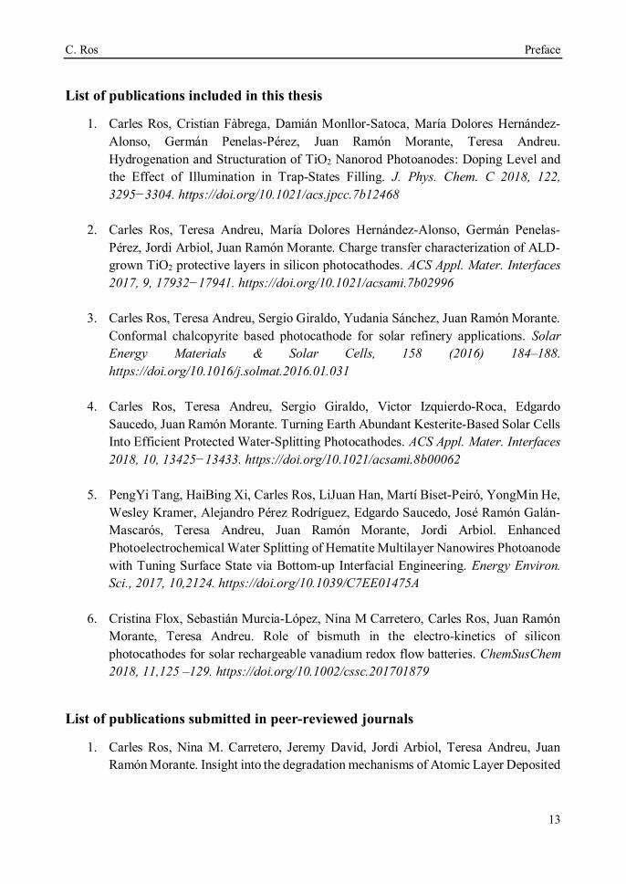
List of publications included in this thesis
1. Carles Ros, Cristian Fàbrega, Damián Monllor-Satoca, María Dolores Hernández-Alonso, Germán Penelas-Pérez, Juan Ramón Morante, Teresa Andreu. Hydrogenation and Structuration of TiO2 Nanorod Photoanodes: Doping Level and the Effect of Illumination in Trap-States Filling. J. Phys. Chem. C 2018, 122, 3295−3304. https://doi.org/10.1021/acs.jpcc.7b12468
2. Carles Ros, Teresa Andreu, María Dolores Hernández-Alonso, Germán Penelas-
Pérez, Jordi Arbiol, Juan Ramón Morante. Charge transfer characterization of ALD-grown TiO2 protective layers in silicon photocathodes. ACS Appl. Mater. Interfaces 2017, 9, 17932−17941. https://doi.org/10.1021/acsami.7b02996
3. Carles Ros, Teresa Andreu, Sergio Giraldo, Yudania Sánchez, Juan Ramón Morante.
Conformal chalcopyrite based photocathode for solar refinery applications. Solar Energy Materials & Solar Cells, 158 (2016) 184–188. https://doi.org/10.1016/j.solmat.2016.01.031
4. Carles Ros, Teresa Andreu, Sergio Giraldo, Victor Izquierdo-Roca, Edgardo
Saucedo, Juan Ramón Morante. Turning Earth Abundant Kesterite-Based Solar Cells Into Efficient Protected Water-Splitting Photocathodes. ACS Appl. Mater. Interfaces 2018, 10, 13425−13433. https://doi.org/10.1021/acsami.8b00062
5. PengYi Tang, HaiBing Xi, Carles Ros, LiJuan Han, Martí Biset‐Peiró, YongMin He,
Wesley Kramer, Alejandro Pérez Rodríguez, Edgardo Saucedo, José Ramón Galán‐Mascarós, Teresa Andreu, Juan Ramón Morante, Jordi Arbiol. Enhanced Photoelectrochemical Water Splitting of Hematite Multilayer Nanowires Photoanode with Tuning Surface State via Bottom‐up Interfacial Engineering. Energy Environ. Sci., 2017, 10,2124. https://doi.org/10.1039/C7EE01475A
6. Cristina Flox, Sebastián Murcia-López, Nina M Carretero, Carles Ros, Juan Ramón
Morante, Teresa Andreu. Role of bismuth in the electro‐kinetics of silicon photocathodes for solar rechargeable vanadium redox flow batteries. ChemSusChem 2018, 11,125 –129. https://doi.org/10.1002/cssc.201701879
List of publications submitted in peer-reviewed journals
1. Carles Ros, Nina M. Carretero, Jeremy David, Jordi Arbiol, Teresa Andreu, Juan Ramón Morante. Insight into the degradation mechanisms of Atomic Layer Deposited
Preface C. Ros
14
TiO2 as photoanode protective layer. Submitted to ACS Appl. Mater. Interfaces. Under revision.
2. Carles Ros, Teresa Andreu, Jeremy David, Jordi Arbiol, Juan Ramón Morante. About degradation and regeneration mechanisms of NiO protective layers deposited by ALD on photoanodes. Under submission.
List of patents
1. SUBSTRATE-ELECTRODE (SE) INTERFACE ILLUMINATED PHOTOELECTRODES AND PHOTOELECTROCHEMICAL CELLS. Application Number EP15382658.1. Holder: Repsol, S.A. G. Penelas Pérez, M.D. Hernández Alonso, T. Andreu, J. R. Morante, C. Ros, N.M. Carretero, E. Calle, P. Ortega, R. Alcubilla. Date of filling: 23-12-2015. International patent: WO/2017/109108. International publication date: 29-6-2017.
C. Ros Preface
15
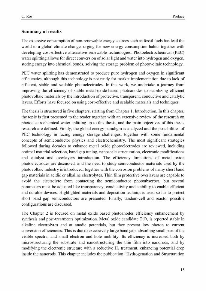
Summary of results
The excessive consumption of non-renewable energy sources such as fossil fuels has lead the world to a global climate change, urging for new energy consumption habits together with developing cost-effective alternative renewable technologies. Photoelectrochemical (PEC) water splitting allows for direct conversion of solar light and water into hydrogen and oxygen, storing energy into chemical bonds, solving the storage problem of photovoltaic technology.
PEC water splitting has demonstrated to produce pure hydrogen and oxygen in significant efficiencies, although this technology is not ready for market implementation due to lack of efficient, stable and scalable photoelectrodes. In this work, we undertake a journey from improving the efficiency of stable metal-oxide-based photoanodes to stabilizing efficient photovoltaic materials by the introduction of protective, transparent, conductive and catalytic layers. Efforts have focused on using cost-effective and scalable materials and techniques.
The thesis is structured in five chapters, starting from Chapter 1, Introduction. In this chapter, the topic is first presented to the reader together with an extensive review of the research on photoelectrochemical water splitting up to this thesis, and the main objectives of this thesis research are defined. Firstly, the global energy paradigm is analyzed and the possibilities of PEC technology in facing energy storage challenges, together with some fundamental concepts of semiconductor physics and electrochemistry. The most significant strategies followed during decades to enhance metal oxide photoelectrodes are reviewed, including optimal material selection, band gap tuning, nanoscale structuration, electronic modifications and catalyst and overlayers introduction. The efficiency limitations of metal oxide photoelectrodes are discussed, and the need to study semiconductor materials used by the photovoltaic industry is introduced, together with the corrosion problems of many short band gap materials in acidic or alkaline electrolytes. Thin film protective overlayers are capable to avoid the electrolyte from contacting the semiconductor photoabsorber, but several parameters must be adjusted like transparency, conductivity and stability to enable efficient and durable devices. Highlighted materials and deposition techniques used so far to protect short band gap semiconductors are presented. Finally, tandem-cell and reactor possible configurations are discussed.
The Chapter 2 is focused on metal oxide based photoanodes efficiency enhancement by synthesis and post-treatments optimization. Metal oxide candidate TiO2 is reported stable in alkaline electrolytes and at anodic potentials, but they present low photon to current conversion efficiencies. This is due to excessively large band gap, absorbing small part of the visible spectra, and small electron and hole mobility. Its efficiency is increased both by microstructuring the substrate and nanostructuring the thin film into nanorods, and by modifying the electronic structure with a reductive H2 treatment, enhancing potential drop inside the nanorods. This chapter includes the publication “Hydrogenation and Structuration
Preface C. Ros
16
of TiO2 Nanorod Photoanodes: Doping Level and the Effect of Illumination in Trap-States Filling”.
In Chapter 3 the strategy is shifted into stabilizing highly efficient short band gap semiconductor materials used by the photovoltaic industry. Silicon based photocathodes are protected by TiO2 overlayers grown by atomic layer deposition (ALD). The deposition parameters are optimized and temperature is found to play a key role for both efficient film conductivity and stability, being this caused by polycrystalline films formation if sufficient thermal energy is available for crystalline reorganization. ALD enabled high thickness control and pinhole-free layers, together with lower crystallization temperatures (starting at less than 200 ºC) than other techniques. The TiO2-Si interface is studied by high resolution transmission electron microscope (HRTEM) imaging and thin 5 nm Ti interlayer is found to suppress detrimental native SiO2 formation and enhance TiO2 nucleation, both beneficial for efficient charge transport from n+-Si to TiO2. This chapter includes the publication “Charge transfer characterization of ALD-grown TiO2 protective layers in silicon photocathodes”.
Chapter 4 is devoted to implementing thin film chalcogenide solar cells into PEC water splitting. Copper-indium-gallium-selenide (CIGS) solar cells fabricated on flexible stainless steel substrates are protected from corrosion by TiO2 ALD protective layers. The transparent conductive oxide (TCO) already used in solar cells is found necessary for efficient p-n junction formation and charge transport to the hydrogen evolution reaction. Copper-zinc-tin-sulfide/selenide (CZTS/Se) solar cells, where scarce indium and gallium are substituted by tin and zinc, are implemented for PEC devices with TiO2 overlayers too. Modifying the S/Se ratio, band gap can be tuned, an especially interesting characteristic for designing tandem PEC devices. The maximum deposition temperature is found at 200 ºC, due to affecting the optimized crystallographic imperfection distribution of original cells, particularly affecting the pure sulfide one. Thanks to the possibility to fabricate both solar cells and PEC electrodes based on the same structure, the TiO2 overlayers and catalyst contributions to electrical and electrochemical charge transfer can be measured, and a series circuit model is presented. This chapter includes the publications “Conformal chalcopyrite based photocathode for solar refinery applications” and “Turning earth abundant kesterite-based solar cells into efficient protected water-splitting photocathodes”.
In Chapter 5, the last one of this thesis, the performance of ALD deposited protective layers is studied in anodic polarizations and alkaline electrolytes. Silicon is used as reference photoabsorber thanks to being unaffected by the used deposition temperatures, 100-300 ºC both for TiO2 and NiO films. In the first work, silicon photoanodes are protected by 100 nm TiO2 films and 5 nm NiFe is used as catalyst. By varying the deposition temperature of TiO2, completely amorphous, mixed amorphous and crystalline and fully crystalline films are deposited, and a clear conductivity increase is observed correlated to crystallization. By conductivity atomic force microscopy (c-AFM) preferential conductivity paths are observed

C. Ros Preface
17
inside crystalline grains, proposed to be related to crystalline defects and grain boundaries. Few hundred hours stability tests revealed significant photocurrent decrease, with no observed dissolution of the Si photoabsorber by scanning electron microscope (SEM). Electrochemical impedance spectroscopy (EIS) revealed an increase of the capacity corresponding to TiO2 depletion increase. This is attributed to oxidative potentials and electrolyte hydroxides diminishing the n-type semiconductor behavior of TiO2 and forming a barrier to charge injection into the oxygen evolution reaction. UV superimposed illumination partially recovered conductivity, a persistent photoconductivity effect which could be used to improve photoanodes stability. In the second work included in this chapter, NiO films are ALD-deposited on Si photoanodes. The temperature deposition is studied and conductivity is found to decrease when temperature is increased from 100 to 300 ºC, simultaneous to a change in preferential crystal growth direction. Both effects are attributed to a higher stoichiometric film being formed when increasing temperature, decreasing Ni2+ vacancies, responsible of the p-type semiconductor behavior. 100 ºC deposited films permitted impressive over 1000 hours stability measurements in highly alkaline electrolyte and at anodic potentials. Periodic cyclic voltammetries are found necessary to avoid partial deactivation of the photoanodes, attributed to chemical modifications at the surface in such highly oxidative conditions. This chapter includes two works just submitted in peer-reviewed journals at the moment of finishing this thesis, “Insight into the degradation mechanisms of Atomic Layer Deposited TiO2 as photoanode protective layer” and “About degradation and regeneration mechanisms of NiO protective layers deposited by ALD on photoanodes”.
The last chapter of this thesis includes the conclusions of the research. In the annex, two other works published in collaboration and a patent are included, which are considered better suited outside the main part of the thesis, since they are the result of collaborative work coming from the knowledge gained through the development of the PhD work.

Preface C. Ros
18
C. Ros Preface
19
Authors’ contribution to the publications included in this thesis
Chapter 2
1. Carles Ros, Cristian Fàbrega, Damián Monllor-Satoca, María Dolores Hernández-Alonso, Germán Penelas-Pérez, Juan Ramón Morante, Teresa Andreu. Hydrogenation and Structuration of TiO2 Nanorod Photoanodes: Doping Level and the Effect of Illumination in Trap-States Filling. J. Phys. Chem. C 2018, 122, 3295−3304.
Impact factor 2018: 4.309 1st quartile by the Journal Citation Report (JCR) in categories: materials
science. Carles Ros performed the synthesis and characterization and wrote the
manuscript. Chapter 3
2. Carles Ros, Teresa Andreu, María Dolores Hernández-Alonso, Germán Penelas-Pérez, Jordi Arbiol, Juan Ramón Morante. Charge transfer characterization of ALD-grown TiO2 protective layers in silicon photocathodes. ACS Appl. Mater. Interfaces 2017, 9, 17932−17941.
Impact factor 2017: 8.097 1st quartile by the Journal Citation Report (JCR) in categories: materials
science and nanoscience and nanotechnology. Carles Ros designed the experiments, performed the ALD synthesis of the
protective layers, catalyst incorporation and device encapsulation optimization. Also, performed characterization (Except HRTEM) and wrote the manuscript.
Chapter 4
3. Carles Ros, Teresa Andreu, Sergio Giraldo, Yudania Sánchez, Juan Ramón Morante. Conformal chalcopyrite based photocathode for solar refinery applications. Solar Energy Materials & Solar Cells, 2016, 158, 184–188.
Impact factor 2016: 4.784 1st quartile by the Journal Citation Report (JCR) in categories: materials
science, energy and fuels and applied physics.

Preface C. Ros
20
Carles Ros designed the experiments, performed the ALD synthesis of the protective layers, catalyst incorporation and device encapsulation optimization. Also, performed characterization and wrote the manuscript.
4. Carles Ros, Teresa Andreu, Sergio Giraldo, Victor Izquierdo-Roca, Edgardo
Saucedo, Juan Ramón Morante. Turning Earth Abundant Kesterite-Based Solar Cells Into Efficient Protected Water-Splitting Photocathodes. ACS Appl. Mater. Interfaces 2018, 10, 13425−13433.
Impact factor 2018: 8.456 1st quartile by the Journal Citation Report (JCR) in categories: materials
science and nanoscience and nanotechnology. Carles Ros designed the experiments, performed the ALD synthesis of the
protective layers, catalyst incorporation and device encapsulation. Also, performed characterization (Except the Raman scattering analysis part) and wrote the manuscript.
Chapter 5
5. Carles Ros, Nina M. Carretero, Jeremy David, Jordi Arbiol, Teresa Andreu, Juan Ramón Morante. Insight into the degradation mechanisms of Atomic Layer Deposited TiO2 as photoanode protective layer. Submitted to ACS Appl. Mater. Interfaces. Under revision.
Carles Ros designed the experiments, performed the ALD synthesis of the protective layers, catalyst incorporation and device encapsulation. Also, performed characterization (except HRTEM) and wrote the manuscript.
6. Carles Ros, Teresa Andreu, Jeremy David, Jordi Arbiol, Juan Ramón Morante. About degradation and regeneration mechanisms of NiO protective layers deposited by ALD on photoanodes. Under submission.
Carles Ros designed the experiments, device encapsulation and characterization (except HRTEM) and wrote the manuscript.
Annex
7. PengYi Tang, HaiBing Xi, Carles Ros, LiJuan Han, Martí Biset‐Peiró, YongMin He, Wesley Kramer, Alejandro Pérez Rodríguez, Edgardo Saucedo, José Ramón Galán‐Mascarós, Teresa Andreu, Juan Ramón Morante, Jordi Arbiol. Enhanced Photoelectrochemical Water Splitting of Hematite Multilayer Nanowires Photoanode

C. Ros Preface
21
with Tuning Surface State via Bottom‐up Interfacial Engineering. Energy Environ. Sci., 2017, 10, 2124.
Impact factor 2017: 30.067 1st quartile by the Journal Citation Report (JCR) in categories: chemistry,
energy and fuels, chemical engineering and environmental sciences. Carles Ros participated in the synthesis process by ALD depositing TiO2
thin-films on the hematite photoelectrodes. Also took part in the results discussion and manuscript revision.
8. Cristina Flox, Sebastián Murcia-López, Nina M Carretero, Carles Ros, Juan Ramón Morante, Teresa Andreu. Role of bismuth in the electro‐kinetics of silicon photocathodes for solar rechargeable vanadium redox flow batteries. ChemSusChem 2018, 11, 125 –129.
Impact factor 2017: 7.411 1st quartile by the Journal Citation Report (JCR) in categories: chemistry and
green & sustainable science & technology. Carles Ros fabricated the photoelectrodes and contributed in results
discussion and manuscript revision. The article in annex chapter by P. Tang et al. is included in his thesis. None of the other articles has been previously used by other co-authors for their doctoral thesis. Barcelona, 28/06/2019 Dr. Teresa Andreu Prof. Juan Ramón Morante

Preface C. Ros
22

C. Ros Preface
23
Resum de la tesi
L’excessiu consum de fonts d’energia no renovables, com ara els combustibles fòssils, ha portat el mon cap a un canvi climàtic que ens urgeix a canviar els hàbits de consum energètic i a desenvolupar tecnologies alternatives que siguin renovables. La fotoelectròlisi de l’aigua (PEC) permet una conversió directa de la llum solar i l’aigua en hidrogen i oxigen, emmagatzemant l’energia en l’enllaç químic, resolent el problema d’emmagatzematge de la tecnologia fotovoltaica.
La fotoelectròlisi de l’aigua ha demostrat la producció eficient d’hidrogen i oxigen purs, però no està preparada per ser implementada a escala de mercat per manca de fotoelèctrodes eficients, estables i escalables. En aquest treball recorrerem el camí des de millorar l’eficiència de fotoànodes estables basats en òxids metàl·lics cap a l’estabilització materials fotovoltaics estables mitjançant capes protectores, transparents, conductores i catalítiques. Els esforços s’han centrat en utilitzar materials i tècniques escalables i rentables en cost-eficiència.
La tesi està estructurada en cinc capítols, començant pel Capítol 1, Introducció. En aquest capítol, el tema es presenta al lector juntament amb una revisió extensa de la recerca en fotoelectròlisi de l’aigua fins al punt d’aquesta tesi, i es plantegen l’àmbit i els objectius d’aquesta tesi. Inicialment s’analitza l’estat del model energètic global i les possibilitats de la fotoelectròlisi davant els reptes de l’emmagatzematge de l’energia, juntament amb conceptes fonamentals de la física i l’electroquímica. S’analitzen les estratègies més destacables que s’han utilitzat durant les últimes dècades per millorar els fotoelèctrodes basats en òxids metàl·lics, incloent la selecció de materials òptims, l’adaptació de l’ample de banda prohibida, l’estructuració a escala nanomètrica, les modificacions de l’estructura electrònica i la introducció de catalitzadors i capes extres d’altres materials. Les limitacions en quant a eficiència dels òxids metàl·lics es discuteixen, i s’introdueix la necessitat d’estudiar materials semiconductors dels utilitzats per la industria fotovoltaica, juntament amb els problemes que aquests materials d’ample de banda petit presenten en quant a corrosió en electròlits àcids i alcalins. Les capes fines protectores poden evitar que l’electrolit entri en contacte amb el semiconductor fotoabsorbidor, però hi ha diversos paràmetres que cal complir com transparència, conductivitat i estabilitat per permetre dispositius eficients i duradors. Es presenten els materials i tècniques més destacats per protegir semiconductors d’ample de banda petit. Finalment, es discuteixen les possibles configuracions de cel·la en tàndem i del reactor.
El Capítol 2 es centra en la millora de l’eficiència de fotoànodes basats en òxids metàl·lics via l’optimització dels mètodes de síntesi i els post-tractaments. Els fotoànodes de TiO2 son coneguts com a estables en electròlits alcalins i a potencials anòdics, però manquen conversions eficients dels fotons en corrent. Això es deu a un ample de banda excessivament gran, que absorbeix només una petita part de l’espectre visible, i una reduïda mobilitat electrònica i dels forats dins del material. S’incrementa l’eficiència tant mitjançant

Preface C. Ros
24
l’estructuració micromètrica del substrat, la nanomètrica de la capa en nanobarres, i modificant l’estructura electrònica via un tractament reductiu en H2 que incrementa la caiguda de potencial dins la nanobarra. Aquest capítol inclou la publicació “Hidrogenat i estructurat de fotoànodes de nanobarres de TiO2: nivell de dopatge i l’efecte de la il·luminació en saturar estats trampa”.
En el Capítol 3 l’estratègia es reorienta cap a estabilitzar materials semiconductors eficients d’ample de banda petit. Fotocàtodes basats en silici son protegits per capes de TiO2 crescudes per dipòsit de capa atòmica (ALD). S’optimitzen els paràmetres i es troba que la temperaura es clau tant per bona conductivitat com estabilitat de la capa, causat per la formació de capes policristal·lines si es disposa de suficient energia tèrmica per la reordenació cristal·logràfica. L’ALD permet un elevat control del gruix de la capa i minimitzar-ne els forats, així com temperatures de cristal·lització menors (començant a menys de 200 ºC) que altres tècniques. La interfase TiO2-Si s’estudia per microscòpia de transmissió electrònica d’altra resolució (HRTEM) i s’observa com les capes intermèdies de 5 nm de Ti eviten la formació de SiO2 nadiu i incrementen la nucleació del TiO2, ambdues coses beneficials per una transferència de càrrega eficient del n+-Si al TiO2. Aquest capítol inclou la publicació “Caracterització de la transferència de càrrega de capes protectores de TiO2 crescudes per ALD en fotocàtodes de silici”.
El Capítol 4 es dedica a implementar cel·les solars de capes fines de calcogenurs en la fotoelectròlisi de l’aigua. Cel·les solars de coure-indi-gal·li-seleni (CIGS) fabricades en substrats flexibles d’acer inoxidable son protegides de la corrosió de l’electròlit mitjançant capes protectores de TiO2 fabricades via ALD. L’òxid transparent i conductor (TCO) ja present a la cel·la solar és necessari per la formació d’unions p-n eficients i pel transport de càrregues a la reacció d’evolució d’hidrogen. Cel·les solars de coure-zinc-estany-sofre/seleni (CZTS/Se), on els materials escassos indi i gal·li son substituïts per zinc i estany son implementades per la fotoelectròlisi també amb capes de TiO2. Variant el rati de S/Se es pot modificar l’ample de banda, una característica especialment interessant per formar cel·les en configuració tàndem. La temperatura màxima de dipòsit va resultar 200 ºC, ja que afecta la distribució cristal·logràfica optimitzada d’imperfeccions de les cel·les originals, afectant especialment la mostra de pur sofre. Gràcies a la possibilitat de fabricar cel·les solars i elèctrodes fotoelectroquímics basant-nos en la mateixa estructura, es poden mesurar les contribucions de la capa protectora de TiO2 i del catalitzador a la transferència de càrrega elèctrica i electroquímica, permetent-nos presentar un model de circuit elèctric en sèrie. Aquest capítol inclou les publicacions “Fotocàtode basat en calcopirites conformals per aplicacions en refineria solar” i “Convertint cel·les solars basades en estructura kesterita i materials abundants en fotocàtodes protegits i eficients per l’electròlisi de l’aigua.
En el capítol 5, l’últim d’aquesta tesi, s’estudia el comportament de capes protectores dipositades via ALD en condicions de treball de polarització anòdica en electròlits alcalins.

C. Ros Preface
25
El silici s’utilitza com a fotoabsorbidor de referència gràcies a que no es veu afectat per les temperatures de dipòsit emprades, entre 100 i 300 ºC tant pel TiO2 com pel NiO. En el primer treball d’aquest capítol es protegeixen fotoànodes de silici amb capes de 100 nm de TiO2 i 5 nm de NiFe s’utilitza com a catalitzador. Modificant la temperatura de dipòsit del TiO2, es dipositen capes completament amorfes, barreja d’amorfa i cristal·lines i completament cristal·lines, i s’observa un clar augment de la conductivitat correlacionat amb la cristal·lització. Mitjançant microscopi de força atòmica de conductivitat (c-AFM) s’observen camins de conductivitat preferent dins dels grans, on es proposa que estan relacionats amb defectes de cristall i fronteres de gra. Els tests d’estabilitat de pocs centenars d’hores mostren una caiguda significativa de la fotocorrent, sense mostrar dissolució del Si en ser observat via microscopi electrònic d’escombrat (SEM). Les mesures d’espectroscòpia d’impedància electroquímica (EIS) mostren un increment de la capacitat corresponent a la depleció en la capa de TiO2. S’atribueix a que els potencials d’oxidació i la incorporació d’hidroxils a la capa redueixen la característica de semiconductor tipus-n del TiO2, formant una barrera per la injecció de les càrregues a la reacció d’evolució d’oxigen. Un extra de llum UV recupera parcialment la conductivitat, un efecte de fotoconductivitat persistent que es podria utilitzar per millorar l’estabilitat dels fotoànodes. En el segon treball d’aquest capítol es dipositen capes de NiO mitjançant ALD en fotoabsorbidors de silici. S’estudia la temperatura de dipòsit i s’observa una reducció de la conductivitat en augmentar de 100 a 300 ºC la temperatura de dipòsit, simultani a un canvi de direcció preferent de creixement cristal·logràfic. Tots dos efectes s’atribueixen a la fabricació de capes més estequiomètriques en augmentar la temperatura, reduint el nombre de vacants Ni2+, les responsables del comportament com a semiconductor tipus-p. Les capes dipositades a 100 ºC van permetre mesures d’estabilitat de més de 1000 h en electròlits altament alcalins i potencials oxidatius. Es va trobar que dur a terme voltametries cícliques de forma periòdica evita una desactivació parcial dels fotoànodes, atribuïda a canvis químics en la superfície en condicions altament oxidants. Aquest capítol inclou dos treballs que, al moment d’acabar aquesta tesi, estan pendents d’acceptació en revistes reconegudes internacionalment, “Percepcions sobre els mecanismes de degradació del TiO2 dipositat via dipòsit de capa atòmica com a capa protectora per fotoànodes” i “Sobre els mecanismes de degradació i regeneració de les capes protectores de NiO dipositades per ALD en fotoànodes.”.
L’últim capítol d’aquesta tesi inclou conclusions de la recerca realitzada. A l’annex, s’inclouen dues altres publicacions fetes en col·laboració i una patent.

Preface C. Ros
26

Chapter 1
Introduction

Chapter 1 C. Ros
28
C. Ros Introduction
29
1. Photoelectrochemical water splitting: introduction
Since the beginning of the industrial revolution, economic growth has been driven by a continuous increase of power consumption1, which has been possible thanks to the availability, high energy density and low price of fossil fuels. The counter part of its exponential consumption increase has been significant alterations of our planet, some of them irreversible. Global climate change attributed to anthropogenic greenhouse gases emission to the atmosphere, rising sea level and temperatures causing ecological unbalance and exponential growth of species extinction rate are examples. In addition, mineral extraction up to scarcity of some specific elements and the consumption of fossil fuels overcoming the “Peak Oil”, the maximum extraction rate (only sustained nowadays by extremely aggressive techniques such as “fracking”) means fossil fuels and some elements easy and cheap extraction is close to come to an end. Some scientists have considered it a new geological era, the Antropocene, due to the scale of human-caused modifications on Earth’s crust and its ecosystems2.
Renewable energy sources and energy saving strategies should be implemented globally, which must be favored by new legislations and technological improvements. Wind, solar and other clean energy sources have in common their intermittent energy production and thus, the need of energy storage technologies to balance energy production and consumption. Converting the surplus energy into chemical bonds such as hydrogen gas allows for later usage, grid distribution or long-periods storage. Being the sun one of the most abundant energy sources, the photoelectrochemical (PEC) water splitting is postulated as one of the most interesting technologies due to worldwide water availability and pollution-free products, enabling hydrogen as a clean energy vector. Currently, most hydrogen gas feedstock is being produced by methane steam reforming, producing CO2 as by-product3, so clean methodologies are of great impact in this field.
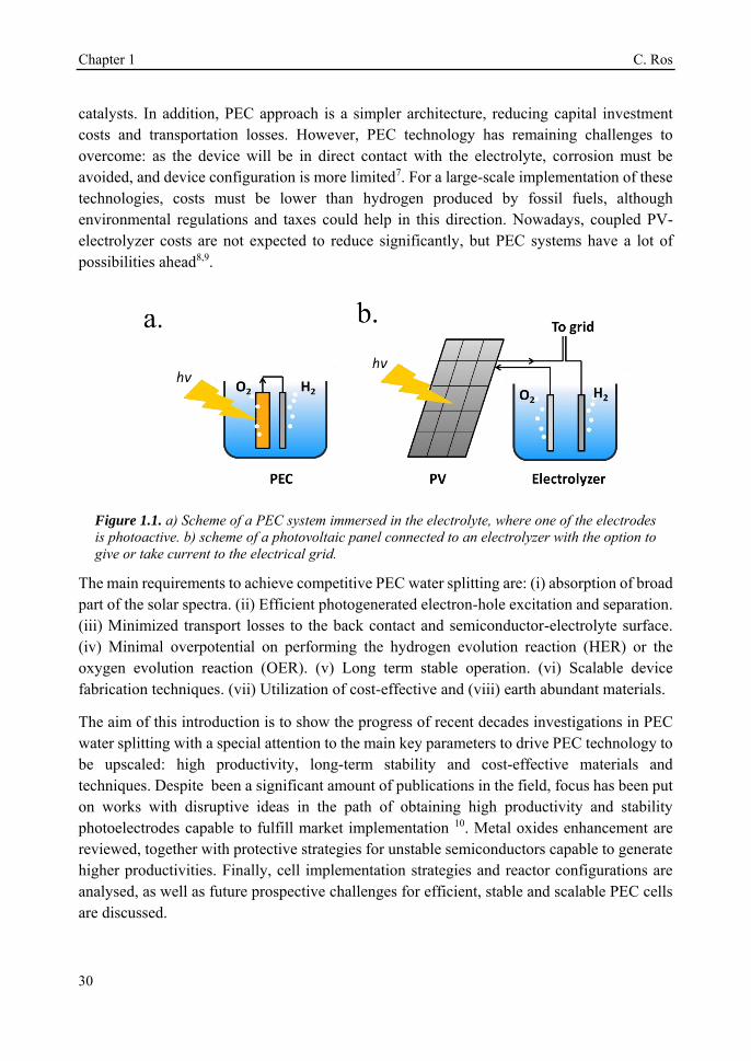
Photoelectrochemical (PEC) water splitting was discovered in the 70’s by Fujishima and Honda4, where TiO2, an n-type semiconductor material with 3 eV band gap, in contact with an electrolyte, was able to absorb photons and generate enough potential to split the water molecule into hydrogen and oxygen, storing solar energy into chemical bonds, named “solar fuel”5. A PEC device can directly convert solar energy into hydrogen and oxygen (Figure 1.1a), although nowadays photovoltaic (PV) cells can be directly coupled to water electrolyzers, such as alkaline electrolysis cells (EC) or proton-exchange-membrane (PEM) electrolyzers6, both techniques consisting in mature technologies, as presented in Figure 1.1b. However, one of the main advantages of PEC is being designed to work at lower current densities, in the range of tens of mA·cm-2, reducing electrochemical overpotentials. This results in lower operation voltages in front of commercial electrolyzers, designed to operate with two orders of magnitude higher currents and thus, significantly higher efficiencies are possible7. Lower current densities enable also low cost and earth abundant alternative
Chapter 1 C. Ros
30
catalysts. In addition, PEC approach is a simpler architecture, reducing capital investment costs and transportation losses. However, PEC technology has remaining challenges to overcome: as the device will be in direct contact with the electrolyte, corrosion must be avoided, and device configuration is more limited7. For a large-scale implementation of these technologies, costs must be lower than hydrogen produced by fossil fuels, although environmental regulations and taxes could help in this direction. Nowadays, coupled PV-electrolyzer costs are not expected to reduce significantly, but PEC systems have a lot of possibilities ahead8,9.
Figure 1.1. a) Scheme of a PEC system immersed in the electrolyte, where one of the electrodes is photoactive. b) scheme of a photovoltaic panel connected to an electrolyzer with the option to give or take current to the electrical grid.
The main requirements to achieve competitive PEC water splitting are: (i) absorption of broad part of the solar spectra. (ii) Efficient photogenerated electron-hole excitation and separation. (iii) Minimized transport losses to the back contact and semiconductor-electrolyte surface. (iv) Minimal overpotential on performing the hydrogen evolution reaction (HER) or the oxygen evolution reaction (OER). (v) Long term stable operation. (vi) Scalable device fabrication techniques. (vii) Utilization of cost-effective and (viii) earth abundant materials.
The aim of this introduction is to show the progress of recent decades investigations in PEC water splitting with a special attention to the main key parameters to drive PEC technology to be upscaled: high productivity, long-term stability and cost-effective materials and techniques. Despite been a significant amount of publications in the field, focus has been put on works with disruptive ideas in the path of obtaining high productivity and stability photoelectrodes capable to fulfill market implementation 10. Metal oxides enhancement are reviewed, together with protective strategies for unstable semiconductors capable to generate higher productivities. Finally, cell implementation strategies and reactor configurations are analysed, as well as future prospective challenges for efficient, stable and scalable PEC cells are discussed.
C. Ros Introduction
31
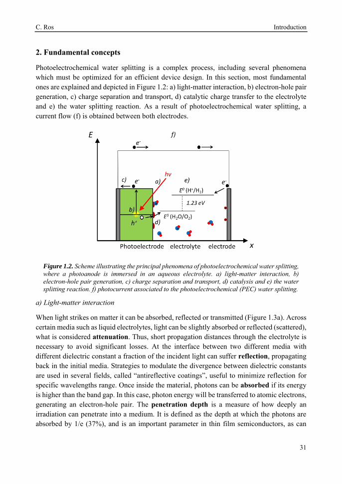
2. Fundamental concepts
Photoelectrochemical water splitting is a complex process, including several phenomena which must be optimized for an efficient device design. In this section, most fundamental ones are explained and depicted in Figure 1.2: a) light-matter interaction, b) electron-hole pair generation, c) charge separation and transport, d) catalytic charge transfer to the electrolyte and e) the water splitting reaction. As a result of photoelectrochemical water splitting, a current flow (f) is obtained between both electrodes.
Figure 1.2. Scheme illustrating the principal phenomena of photoelectrochemical water splitting, where a photoanode is immersed in an aqueous electrolyte. a) light-matter interaction, b) electron-hole pair generation, c) charge separation and transport, d) catalysis and e) the water splitting reaction. f) photocurrent associated to the photoelectrochemical (PEC) water splitting.
a) Light-matter interaction
When light strikes on matter it can be absorbed, reflected or transmitted (Figure 1.3a). Across certain media such as liquid electrolytes, light can be slightly absorbed or reflected (scattered), what is considered attenuation. Thus, short propagation distances through the electrolyte is necessary to avoid significant losses. At the interface between two different media with different dielectric constant a fraction of the incident light can suffer reflection, propagating back in the initial media. Strategies to modulate the divergence between dielectric constants are used in several fields, called “antireflective coatings”, useful to minimize reflection for specific wavelengths range. Once inside the material, photons can be absorbed if its energy is higher than the band gap. In this case, photon energy will be transferred to atomic electrons, generating an electron-hole pair. The penetration depth is a measure of how deeply an irradiation can penetrate into a medium. It is defined as the depth at which the photons are absorbed by 1/e (37%), and is an important parameter in thin film semiconductors, as can
Chapter 1 C. Ros
32
range from 2 µm for Si (at 555 nm wavelengths) to down to few nanometers for iron oxide. The non-reflected or absorbed light is considered transmitted.
b) Electron-hole pair excitation
If a material absorbs a photon, the energy is transferred to an electron, which is excited to a higher energy level. In a semiconductor’s case, electron states from individual atoms have an overall average energy state distribution forming a valence band (EV) and a conduction band (EC), highest energy states occupied and lowest energy vacant states at absolute zero temperature, respectively. The energy difference between these two bands, where no states are present, is the forbidden energy region, named the band gap (Eg).
After photon absorption, some of the valence band electrons (e-) are excited into the conduction band leaving an empty state in the network of covalent bonds, considered a “hole” (h+). If photon’s energy is larger than the band gap, the electron will dissipate that extra energy (“thermalize”) until stabilizing in the conduction band, giving that extra energy to neighbor atoms in the form of thermal vibration and thus, not storing all original photon’s energy in the excited electron-hole pair.
For semiconductors at a certain temperature, some of these atoms are spontaneously ionized, where electrons are excited to the conduction band and holes are created in the valence band. The nature of the majority carriers formed, i.e. free electrons or vacancies in the covalent structure, determines the n- or p-type semiconductor behavior. This is normally governed by alterations in the crystal lattice material covalent network, where modifying the amount of acceptors (accepting a free electron) or donors (giving free electrons) is named “doping” the semiconductor, and there are several forms to do it. Among them, the presence of an element with different number of valence electrons (i.e.: a boron atom with 3 electrons in the external shell in a silicon covalent structure consisting on 4-links per atom results in an electron missing in the covalent bonding) or the formation of a sub-stoichiometric material (i.e.: oxygen vacancies in TiO2 are the responsible of n-type semiconductor behavior). The average states distribution energy is called the Fermi level (EF). If Fermi level is closer to the valence band and majority carriers are holes it is considered a p-type semiconductor, and if it is closer to conduction band and electrons are majority carriers, an n-type one.
c) Charge separation and transport
Light-induced electron hole pairs need to be separated to avoid eventual recombination, the process in which the excited electron releases its energy, “filling” a hole back in the valence band. High recombination rates make impossible to extract any current from photogenerated charges, thus efficient charge separation is needed. Thus, an external potential can be applied, or an internal built-in potential can be used to spontaneously separate photogenerated charges and consequently, to create a photovoltage and a photocurrent. By putting in contact a p-type and an n-type semiconductors a p-n junction is formed, where the average amount

C. Ros Introduction
33
of free electrons or holes (Fermi levels) is equilibrated by charges diffusing from one to the other, forming a space-charge or depletion region where there is a strong electric field (Figure 1.3b).
There are several structures forming built-in electric fields, among them:
- p-n homojunction, where a semiconductor has two regions with different type character (i.e. p-type and n-type silicon).
- p-n heterojunction, where two different materials of different type character are in contact (i.e. n-type TiO2 and p-type silicon).
- Schottky junction, where a semiconductor equilibrates with the free electrons energy level of a metallic film (i.e. Ni metal and n-type silicon).
- A semiconductor-liquid junction (SCLJ), where the semiconductor equilibrates with the ions adsorbed in the surface, forming a Helmholtz double layer (i.e. n-type TiO2 in an alkaline electrolyte).
Figure 1.3. a) Scheme of a light beam incident on a two different mediums interface with different refractive index, depicting incident, reflected, absorbed and transmitted light and the formation of an electron-hole pair. b) Energy band diagram of a p-n junction presenting a photon absorbed and the movement of the electron and hole under the built-in electric field, together with the photogenerated voltage between Fermi levels.
Formed electric fields will drift generated charges to opposite directions, i.e. electrons to surface and holes to the back contact (Figure 1.3b). For efficient charge transport, high conductivity is needed. Conductivity is governed by both carrier mobility and carrier
Chapter 1 C. Ros
34
concentration. Carrier mobility highly depends on impurities and defect concentration: electrons and holes highly scatter on crystallographic defects such as interstitial atoms or vacancies, plane dislocations, stacking faults or grain boundaries, losing some energy and changing direction. Meanwhile, carrier concentration is determined by the doping level, temperature and illumination intensity. All these parameters will be reflected in a higher resistance to charge transport.
d) Catalysis and catalyst introduction
Once the electrons/holes reach the surface of the photoabsorber, a chemical reaction takes place. In water splitting, the hydrogen or oxygen evolution reaction, respectively. So, not only the charge separation and transport of electrons/holes to the surface is crucial but also, the efficiency of the water splitting reaction and how the electrons are transferred to the reactants to obtain the products. In this sense, catalysts play an important role, accelerating a chemical reaction.
An electrocatalyst is defined as a material repeatedly enhancing a certain reaction without being consumed. Catalysts introduce alternative reaction paths with lower activation energy through forming alternative intermediate species on its surface. As the reaction will happen on the surface, normally very small amounts of catalysts are needed.
e) The water splitting reaction
The water splitting reaction (2𝐻2𝑂 → 2𝐻2(𝑔) + 𝑂2(𝑔) (𝑒𝑞. 1)) is a non spontaneous reaction. At room temperature, water can be split by applying an electrical potential between two electrical contacts, a cathode and an anode, immersed in an aqueous electrolyte, to drive two half-reactions, the hydrogen evolution reaction (HER) and oxygen evolution reaction (OER) (Figure 1.1a and Figure 1.4a). The complete reaction has a Gibbs free energy of 237.18 kJ per mol of produced 𝐻2, corresponding to a thermodynamic reversible potential of 1.23 V. However, this value is theoretical, assuming ionic concentration of 1 molar, gases pressure of 1 atm. and 298 K, for different conditions, the potential value will vary following the Nernst equation. For instance, at different pHs, the HER and OER standard potential values are:
𝐻𝐸𝑅:
𝑝𝐻 = 0 4𝐻+ + 4𝑒− → 2𝐻2 𝐸0 = 0 𝑉 𝑣𝑠 𝑆𝐻𝐸 (𝑒𝑞. 2)
𝑝𝐻 = 14 4𝐻2𝑂 + 4𝑒− → 2𝐻2 + 4𝑂𝐻− 𝐸0 = −0.83 𝑉 𝑣𝑠 𝑆𝐻𝐸 (𝑒𝑞. 3)
𝑂𝐸𝑅:
𝑝𝐻 = 0 2𝐻2𝑂 → 𝑂2 + 4𝑒− 𝐸0 = 1.23 𝑉 𝑣𝑠 𝑆𝐻𝐸 (𝑒𝑞. 4)
𝑝𝐻 = 14 4𝑂𝐻− → 𝑂2 + 2𝐻2𝑂 𝐸0 = 0.4 𝑉 𝑣𝑠 𝑆𝐻𝐸 (𝑒𝑞. 5)
Also, to drive kinetically efficient these reactions, additional potentials are necessary for the catalysis, 𝜂𝐻𝐸𝑅 and 𝜂𝑂𝐸𝑅, named as overpotentials (~0.4 V at ~10 mA·cm-2 currents for state
C. Ros Introduction
35
of the art catalysts11–17). The overpotential need to drive the reaction efficiently depends not only on the electrocatalyst nature, but also on the basic or acidic character of the electrolyte, the abundance of hydroxides (𝑂𝐻−) or protons (𝐻+), which plays a role on the water dissociation kinetics18. In addition, ionic conductivity is necessary between the two electrodes, which can introduce another extra potential (𝜂𝑖𝑜𝑛𝑖𝑐 𝑐𝑜𝑛𝑑.) for large distances or reduced ion concentration/conductivity, resulting in an ohmic loss. Gases should be separated to avoid back-reactions if they diffuse to the opposite polarized electrode.
Adding all contributions, a minimum required voltage (𝑉𝑚𝑖𝑛) is obtained:
𝑉𝑚𝑖𝑛(𝑗) = 1.23 𝑒𝑉 + 𝜂𝐻𝐸𝑅(𝑗) + 𝜂𝑂𝐸𝑅(𝑗) + 𝜂𝑖𝑜𝑛𝑖𝑐 𝑐𝑜𝑛𝑑.(𝑗)
Record values down to ~1.4 V for a current of around 10 mA·cm-2 have been obtained19,20.
f) Photoelectrochemical (PEC) water splitting
In PEC water splitting, photons absorbed by the semiconductor create electron-hole pairs, which are separated by the built-in electric field inside the photoelectrode, generated in the semiconductor-liquid junction (SCLJ) by semiconductor and electrolyte Fermi level equilibration. A double layer is formed, first described by Helmholtz21 nowadays extended by other authors22 formed by ions physically adsorbed to semiconductor’s surface and a diffuse outer layer with exponentially decreasing potential. Electric neutrality is obtained by band bending generated inside the semiconductor23. The built-in electric field can separate electron-hole pairs, generating photovoltage (Vph) and photocurrent, as depicted in Figure 1.4a and b. In a photoanode, holes are driven to photoelectrode’s surface and perform the oxygen evolution, meanwhile electrons are collected by the back contact and close the circuit performing the proton reduction reaction in the counter electrode. Similarly, if the semiconductor built-in electric field drives electrons to the surface to perform the hydrogen evolution, it is considered a photocathode. For a significant photocurrent injected into the electrolyte to perform the water splitting reaction, photogenerated electron-hole pairs will suffer overpotentials for charge-separation (𝜂𝑠𝑒𝑝) and for charge transport (𝜂𝑡𝑟𝑎𝑛𝑠) across the semiconductor, from the back contact and other elements in the circuit. Some authors have calculated a minimum band gap (𝐸𝑔 𝑚𝑖𝑛) of >2.04 eV23,24 based on:
𝐸𝑔 𝑚𝑖𝑛 = 𝜂𝑡𝑟𝑎𝑛𝑠 + 𝜂𝑠𝑒𝑝 + 𝑉𝑚𝑖𝑛
If the photopotential is generated by a single photoelectrode is not enough, an external bias can be applied to complete the reaction. This way, external power would be used, but it can help in extracting more power from the photoelectrode too.
Independent analysis of each electrode is possible by measuring in a “three electrode” cell configuration (or half cell) (Figure 1.4c), where a reference electrode is used (at a fixed potential in respect to the electrolyte). In this disposition, the required current is applied in the
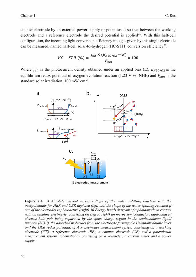
Chapter 1 C. Ros
36
counter electrode by an external power supply or potentiostat so that between the working electrode and a reference electrode the desired potential is applied25. With this half-cell configuration, the incoming light conversion efficiency into gas given by this single electrode can be measured, named half-cell solar-to-hydrogen (HC-STH) conversion efficiency26.
𝐻𝐶 − 𝑆𝑇𝐻 (%) = 𝑗𝑝ℎ × (𝐸𝐻2𝑂/𝑂2 − 𝐸)
𝑃𝑠𝑢𝑛× 100
Where 𝑗𝑝ℎ is the photocurrent density obtained under an applied bias (E), 𝐸𝐻2𝑂/𝑂2 is the equilibrium redox potential of oxygen evolution reaction (1.23 V vs. NHE) and 𝑃𝑠𝑢𝑛 is the standard solar irradiation, 100 mW·cm-2.
Figure 1.4. a) Absolute current versus voltage of the water splitting reaction with the overpotentials for HER and OER depicted (left) and the shape of the water splitting reaction if one of the electrodes is photoactive (right). b) Energy bands diagram of a photoanode in contact with an alkaline electrolyte, consisting on (left to right) an n-type semiconductor, light-induced electron-hole pair being separated by the space-charge region in the semiconductor-liquid junction (SCLJ), the adsorbed molecules from the electrolyte forming the Helmholtz double layer and the OER redox potential. c) A 3-electrodes measurement system consisting on a working electrode (WE), a reference electrode (RE), a counter electrode (CE) and a potentiostat measurement system, schematically consisting on a voltmeter, a current meter and a power supply.
C. Ros Introduction
37
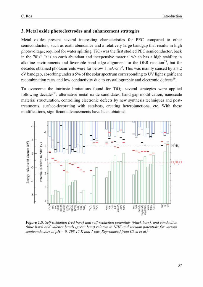
3. Metal oxide photoelectrodes and enhancement strategies
Metal oxides present several interesting characteristics for PEC compared to other semiconductors, such as earth abundance and a relatively large bandgap that results in high photovoltage, required for water splitting. TiO2 was the first studied PEC semiconductor, back in the 70’s4. It is an earth abundant and inexpensive material which has a high stability in alkaline environments and favorable band edge alignment for the OER reaction28, but for decades obtained photocurrents were far below 1 mA·cm-2. This was mainly caused by a 3.2 eV bandgap, absorbing under a 5% of the solar spectrum corresponding to UV light significant recombination rates and low conductivity due to crystallographic and electronic defects29.
To overcome the intrinsic limitations found for TiO2, several strategies were applied following decades30: alternative metal oxide candidates, band gap modification, nanoscale material structuration, controlling electronic defects by new synthesis techniques and post-treatments, surface-decorating with catalysts, creating heterojunctions, etc. With these modifications, significant advancements have been obtained.
Figure 1.5. Self-oxidation (red bars) and self-reduction potentials (black bars), and conduction (blue bars) and valence bands (green bars) relative to NHE and vacuum potentials for various semiconductors at pH = 0, 298.15 K and 1 bar. Reproduced from Chen et al.31

Chapter 1 C. Ros
38
3.1. Metal oxide photoelectrode candidate materials
Among all possible metal oxides, TiO2 (n-type, 3.2 eV)4,32–36 has been always present as one of the most investigated materials, and other candidates have been widely studied too such as Fe2O3 (n-type, 2.2 eV)37–39, ZnO (n-type, 3.3-3.4 eV)40,41, WO3 (n-type, 2.6-2.8 eV)42–44, BiVO4 (n-type, 2.3-2.5 eV)45–48, NiO (p-type, 3.4 eV)49 and Cu2O (p-type, 2.0 eV)50. More materials have been tested but without remarkable success, as there are several criteria to be met: corrosion potentials less favorable than HER/OER reactions, proper band alignment for large photovoltage generation, and favorable band position for the desired redox reaction.
As it can be observed in Figure 1.5, some materials are not useful for water splitting due to unfavorable band alignment, with band edges far from water redox potentials31. To perform the HER reaction, conduction band must be at more negative potentials relative to NHE than the H+/H2 potential (black dashed line), and for the OER, at more positive potentials than O2/H2O (red dashed line). For a bias-free reaction, both conditions must be met.
Bard et al.51, Gerischer et al.52 and other works have discussed in which conditions corrosion reactions are less energetic and thus, thermodynamically more favourable than the HER/OER reaction. S. Chen and L. Wang calculated thermodynamic oxidation and reduction potentials of several semiconductors and compared them to the OER/HER reaction, finding a significant portion of them require protection from corrosion (Figure 1.5) 31. Generally, a photoelectrode is stable to electron reduction if the self-reduction potentials are more negative relative to NHE than either the H+/H2 or conduction band minimum, and to holes oxidation if self-oxidation potentials are more positive than O2/H2O or valence band maximum.
Some of these oxides, having 3 eV or higher band gaps limit their theoretical maximum current to values lower than 1.8 mA·cm-2, such as NiO, TiO2 or ZnO. Alternative interesting candidates in relation to the mentioned parameters are BiVO4, WO3, Fe2O3 and Cu2O, with 2.0-2.5 eV band gaps and theoretical photocurrents over 10 mA·cm-253,54; but they are prone to crystallographic disorder, presenting significant electronic drawbacks: abundant superficial and internal recombination states, low carrier mobility and lifetime. Hence, optimized fabrication of these materials where electronic drawbacks can be overcome has turned into one of the main investigation fields. As an example of photoanode optimization, reducing Fe2O3 thickness or their nanostructuration can overcome the extremely short charge diffusion length and lifetime, reaching up to 4.3 mA·cm-2 at 1.23 V vs RHE, a 34% of its theoretical maximum photocurrent37. Also, WO3 nanocrystals all grown with a (002) facet orientation have demonstrated to avoid multiple surface energies, and thus, OER overpotentials and kinetics42.
Even expecting high stability, thoughtful investigations have observed chemical and performance degradation by high pH electrolytes in photoanodes such as BiVO4 when protective overlayers or cocatalysts are not used55. Further increasing materials complexity

C. Ros Introduction
39
by multiple metal oxides have shown unprecedented photocurrents up to 2.4 mA·cm-2 at 0.4 V vs RHE for CuFeO2 combined with NiFe/reduced graphene oxide layers56, although much more work is needed in this path.
3.2. Band gap modifications
Large band gap metal oxides have energy band positions prone for water splitting, but lack significant visible light harvesting. Thus, many attempts have been made to modify their bandgap and increase their visible light absorption57. Creating new states at energies inside the band gap by forming oxygen vacancies or doping with non-metals or transition metals enable shorter energy differences, thus narrowing the optical band gap. As examples, nitrogen and hydrogen doping on TiO2 was performed by Wang et al, giving a yellowish material and enhancing quantum efficiency in the previously inactive energy wavelengths of 450-600 nm58,59, or S doping occupied oxygen vacancies and narrowed the band gap achieving visible light absorption60, among others61. However, these improvements have not reached more than a few % efficiency increase, as creating states inside the band gap also creates detrimental recombination paths for photogenerated electron-hole pairs. Similar studies on bandgap modification by doping have been performed to other materials such as WO3
62,63 and ZnO64–
66.
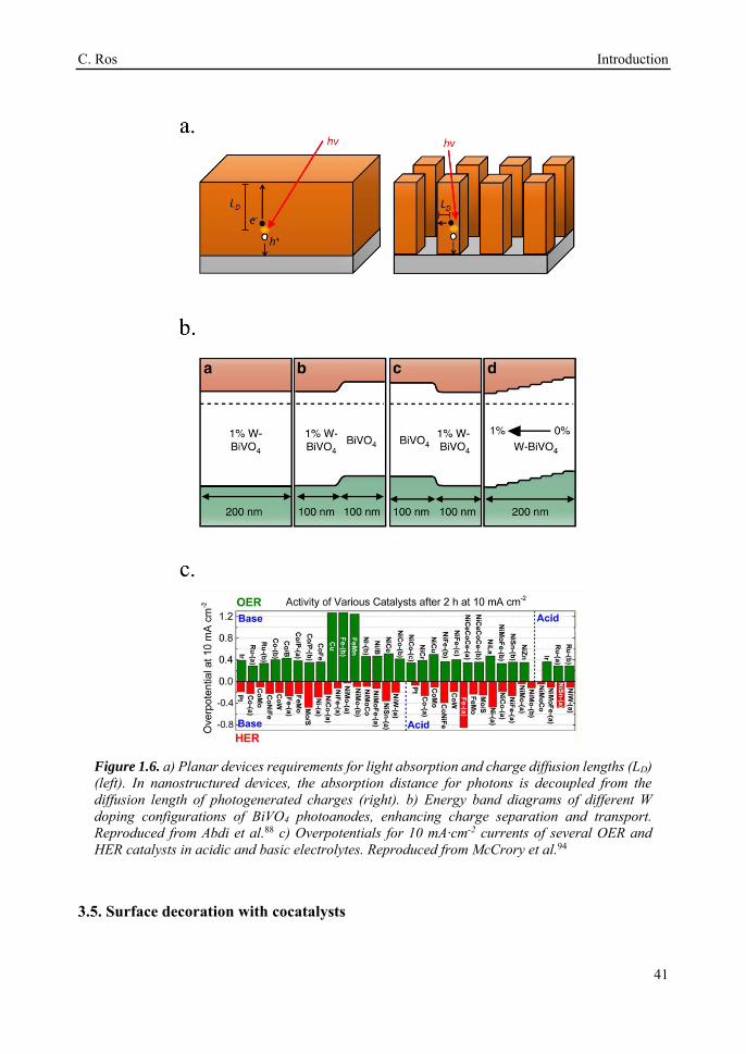
3.3. Nanoscale material structuration
Controlling material optical and electronic properties gave metal oxide photoelectrodes a significant push, but optimizing material’s morphology by controlling growth process at the nanoscale enabled a completely new field. Nanoscale structuration increases the surface area in contact with the electrolyte, reducing electrochemical kinetic overpotentials by lower current densities. Light absorption and charge transport are also enhanced thanks to decoupling light penetration depth and photogenerated charges diffusion length with nanostructures, facilitating charge transport to the electrolyte by enhanced active surface. Planar devices require thicknesses sufficient to absorb of a significant portion of the incident light, and photogenerated charges require diffusion lengths (LD) enough to reach the surface. In nanostructured devices, the absorption distance for photons is decoupled from the diffusion length of photogenerated charges and thus, allow for higher absorptions meanwhile reducing current loss (Figure 1.6a)67. 3D structures such as micrometer-size TiO2 anodization32,59,68–70, rutile TiO2 nanorods hydrothermal growth71–73, WO3 nanowires and nanoflakes43,74, ZnO nanorods40,41,65,66, BiVO4
45, Cu2O53 and Fe2O339,75
have been fabricated with enhanced PEC performance.
For instance, Cu-Ti-O nanotube arrays formed by anodization demonstrated increased active surface (tube length, pore and wall thickness) and light absorption by changing the Cu-Ti percentage, giving photocurrents from 0.035 to 0.065 mA·cm-2 at -1 V vs Ag/AgCl76. Cu2O nanowires protected with ZnO/TiO2/RuO present increased light absorption and charge

Chapter 1 C. Ros
40
separation thanks to nanostrcturation, 5 mA·cm-2 for planar and 8 mA·cm-2 when nanostructured at 0 V vs RHE53,77. By macro-mesoporous optimal structuration, BiVO4 photoanodes obtained photocurrents of 2 mA·cm-2 compared with 0.5 mA·cm-2 at 1 V vs Ag/AgCl of the disordered porous films78. Reducing and controlling material thickness can shorten the electrical path for photogenerated charges. I.e., Fe2O hematite photoanodes, due to few nanometers carrier diffusion lengths, require nanometer-scale thicknesses to minimize recombination loses79,80.
Combining substrate structuration and nanoscale material deposition light absorption and photogenerated charge collection can be improved. High Mo-doped BiVO4 deposition control in nanocone-shaped substrates, together with Fe/NiOOH catalyst and appropriate phosphate buffered electrolyte achieved up to 6 mA·cm-2 at 1.23 V vs RHE81.
3.4. Controlling electronic structure and surface states
To overcome problems such as inefficient charge separation and transport, generating higher and localized potential gradients through electronic doping is key. Metal doping, oxygen vacancy control or hydrogen and nitrogen doping have been studied. α-Fe2O3 has been doped with several cations such as Si, Ti, Pt, Cr, and Mo, finding a decrease of the recombination rate by increasing charge transfer and grain-boundary passivation82–85. Also, partially electrochemical reduction to Fe2O4 (a more conductive phase) can form beneficial conduction paths and reduce recombination86. BiVO4 has been modified both with W and Mo dopants and by hydrogen treatment to form oxygen vacancies. For example, porous BiVO4 can double photoactivity with a 2% Mo incorporation87 and potential gradient can be enhanced by gradual incorporation of W during deposition (Figure 1.6b)88, or from 0.5 up to 4 mA·cm-2 at 1.2 V vs Ag/AgCl by hydrogenation at 300 ºC thanks to increased donor density, enhancing electron-hole separation and transport89. TiO2 electronic band structure has also been intensively studied, where the depletion region was optimized in nanorod structures by vacancy formation under ammonia atmosphere73.
Also, minimizing superficial electronic states, which act as trap states, is interesting to reduce photogenerated electron-hole recombination and thus, enhancing PEC efficiency. This can be achieved controlling the synthesis and post-treatments, and incorporating other metals on the surface to fill the traps and to act as OER catalysts. Fe2O3 photoanodes surface recombination can be reduced by CoOx
90, Ga2O390,91 or TiO2
92 surface states passivation. TiO2 surface recombination rate was improved by removing detrimental chlorine atoms (blocking oxygen evolution active sites) by a 250 ºC annealing treatment71, or by increasing hydroxyl groups acting as hole trap sites after ammonia treatments73. Depositing atomically-thin films covering the surface is also a very effective strategy to supress detrimental superficial states, avoiding recombination paths and contributing to shifts in the band positions of the metal oxide photoelectrode respect to the electrolyte, enhancing obtained potentials93.
C. Ros Introduction
41
Figure 1.6. a) Planar devices requirements for light absorption and charge diffusion lengths (LD) (left). In nanostructured devices, the absorption distance for photons is decoupled from the diffusion length of photogenerated charges (right). b) Energy band diagrams of different W doping configurations of BiVO4 photoanodes, enhancing charge separation and transport. Reproduced from Abdi et al.88 c) Overpotentials for 10 mA·cm-2 currents of several OER and HER catalysts in acidic and basic electrolytes. Reproduced from McCrory et al.94
3.5. Surface decoration with cocatalysts

Chapter 1 C. Ros
42
Photoelectrodes such as Fe2O3, CuO2 or TiO2 have suitable surface states to directly perform the desired reaction, but the use cocatalysts can enhance their performance thanks to favourable superficial energetics, improving reaction kinetics. Examples of these catalysts are Pt, MoS2 or RuOx for the HER reaction and Ni/FeOOH, CoPi or IrOx for the OER (Figure 1.6c)12,29,95–97. Some of these cocatalysts are noble metals (Pt, Ru, Ir…), scarce and expensive for large-scale deployment, what has pushed investigation in earth-abundant alternative efficient electrocatalysts14,9894. In the HER case, photocathodes such as Cu2O have been decorated with Pt (best performing HER catalyst) and RuOx
53, and also earth abundant MoS2 cocatalysts13,94. Tilley et al used RuOx or Pt as catalysts and an AZO/TiO2 protective layer (also forming an heterojunction) to obtain over 0.55 V vs RHE onset potential and 5 mA·cm-
2 photocurrents for Cu2O photocathodes99. Amorphous MoS2 allowed earth-abundant Cu2O for up to 5.7 mA·cm-2 at 0 V vs RHE at pH 1100.
OER reaction is a complex four electron process, with slow kinetics in most of the surfaces80. Enhancing reaction kinetics or reducing potential barriers thanks to cocatalysts have improved the performance of TiO2 and Fe2O3 photoanodes101. For example, hierarchically nanostructured TiO2 photoanodes decorated with Au particles doubled photocurrent up to 2 mA·cm-2 at 1.23 V vs RHE102; or α-Fe2O3 ones obtained up to 15 % current increase and over 200 mV cathodic shift with Cobalt phosphate (Co-Pi) electrocatalyst103. Co-Pi also improved BiVO4 photoanodes performance up to 1.7 mA·cm-2 47,87, and FeOOH catalyst incorporation in a 0.1 M KH2PO4 + 0.1 M Na2SO3 electrolyte, increased BiVO4 anodic photocurrent to 2.0 mA·cm-2 at 1.23 vs RHE46.
3.6. Metal oxide heterojunctions
Up to now, potential improvements of single metal oxides have been analysed, but their combination opens a whole field of opportunities. By the introduction of other materials layers or substrates, charge separation can be improved by forming an heterojunction.
For photoanodes, several authors have studied the WO3/BiVO4 heterojunction, obtaining up to 4 mA·cm-2 at 1.23 V vs RHE, almost doubling productivity obtained by each oxide separately74,104. The band energy difference of the two materials enhances charge separation, and different band gaps allow for increased light absorption. Also, a BiVO4 photoanode with ZnFeO overlayer increased its photocurrent and decreased the onset potential, making it resistant to alkaline electrolytes, sustaining 3 mA·cm-2 at 1.23 V vs RHE45.
For photocathodes, a Cu2O photoelectrode was covered with an AZO/TiO2/Pt multilayer grown by atomic layer deposition (ALD), obtaining stable and up to 2 mA·cm-2 photocurrents at 0 V vs RHE77. Similar structures but on Cu2O nanowires and with RuOx as catalyst increased the photocurrent up to 8 mA·cm-2 at 0 V vs RHE, almost the double than the same Cu2O/AZO/TiO2/RuOx structure on planar photoelectrodes53. Cu2O is a good example on how combining nanostructuration, synthesis optimization, multilayer heterojunction and
C. Ros Introduction
43
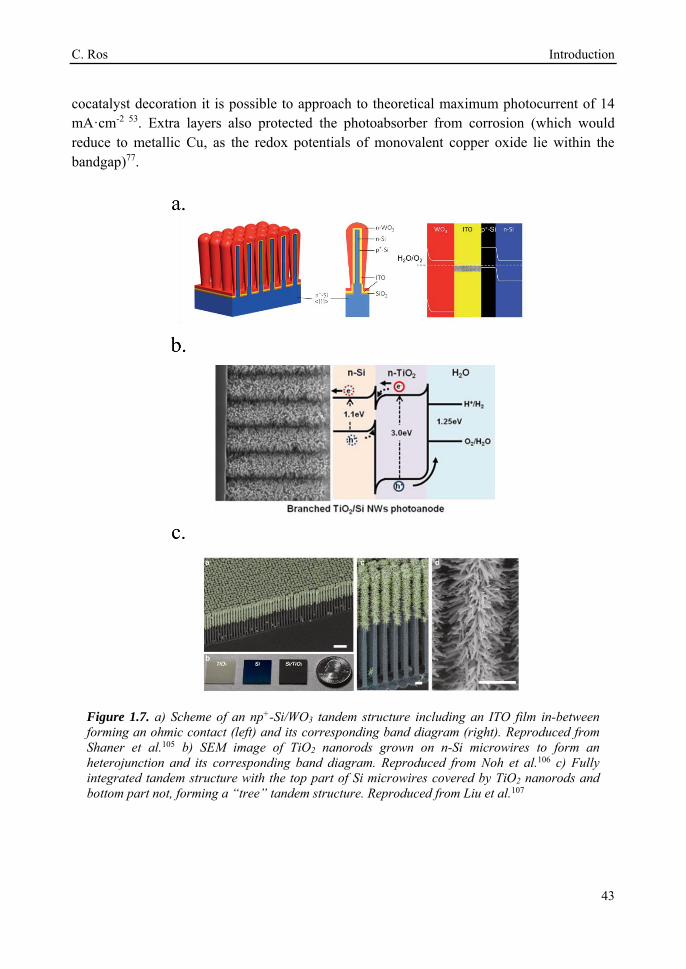
cocatalyst decoration it is possible to approach to theoretical maximum photocurrent of 14 mA·cm-2 53. Extra layers also protected the photoabsorber from corrosion (which would reduce to metallic Cu, as the redox potentials of monovalent copper oxide lie within the bandgap)77.
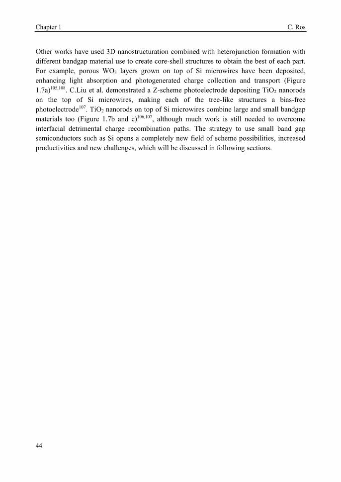
Figure 1.7. a) Scheme of an np+-Si/WO3 tandem structure including an ITO film in-between forming an ohmic contact (left) and its corresponding band diagram (right). Reproduced from Shaner et al.105 b) SEM image of TiO2 nanorods grown on n-Si microwires to form an heterojunction and its corresponding band diagram. Reproduced from Noh et al.106 c) Fully integrated tandem structure with the top part of Si microwires covered by TiO2 nanorods and bottom part not, forming a “tree” tandem structure. Reproduced from Liu et al.107
Chapter 1 C. Ros
44
Other works have used 3D nanostructuration combined with heterojunction formation with different bandgap material use to create core-shell structures to obtain the best of each part. For example, porous WO3 layers grown on top of Si microwires have been deposited, enhancing light absorption and photogenerated charge collection and transport (Figure 1.7a)105,108. C.Liu et al. demonstrated a Z-scheme photoelectrode depositing TiO2 nanorods on the top of Si microwires, making each of the tree-like structures a bias-free photoelectrode107. TiO2 nanorods on top of Si microwires combine large and small bandgap materials too (Figure 1.7b and c)106,107, although much work is still needed to overcome interfacial detrimental charge recombination paths. The strategy to use small band gap semiconductors such as Si opens a completely new field of scheme possibilities, increased productivities and new challenges, which will be discussed in following sections.

C. Ros Introduction
45
4. Short band gap semiconductors for PEC water splitting
In the previous section, strategies to overcome the main drawbacks presented by metal oxide photoelectrodes for water splitting were discussed. The successful materials obtaining photocurrents higher than 8 mA·cm-2 with significant photovoltages are very few. In parallel to PEC water splitting development, science and industry of the photovoltaic field (PV) have optimized photoabsorbers and fabrication techniques up to commercial devices with minimal recombination and transport losses. PV productivities have been based on short band gap materials (1-1.5 eV) capable of absorbing the majority of visible spectrum, with materials achieving large carrier mobility thanks to minimized defects and disorder109–112. Monocrystalline silicon-based solar cells, giving photocurrents over 40 mA·cm-2 and 700 mV open circuit photovoltages are nowadays largely dominating the market thanks to relatively cheap price and material abundance, several years operation stability and efficiencies over 22%. Monocrystalline silicon has not been the only photoabsorber commercialized: polycrystalline and amorphous silicon, together with CdTe, GaAs and CIS/CIGS have been already commercialized, and other semiconductors such as perovskites or CZTSSe are emerging rapidly (Figure 1.8)109.
Figure 1.8. 2019 plot of highest-recorded photovoltaic efficiency by year of various photovoltaic devices classified by technology (colours). Prepared by the National Renewable Energy Laboratory (NREL, www.nrel.gov).
During the last decade, implementing short band gap materials in PEC water splitting has attracted much interest, thanks to all the knowledge and development from PV industry and
Chapter 1 C. Ros
46
thus, the possibility to obtain significantly higher outputs than with metal oxides. Although, the use of these photoabsorbers presents extra challenges added to the photovoltaic ones. Not having a large band gap, and thus photovoltage, will require a tandem structure combining ~1.1 and 1.6-1.8 eV semiconductors photovoltages or an external bias to use all of their capacity, as it will be reviewed in section 8.2, tandem PEC devices. Moreover, monolithic photoelectrodes must be immersed in the electrolyte, preferably in acidic or alkaline electrolytes where the electrochemical activity is highly enhanced. But these electrolytes are normally corrosive for most of the presented photovoltaic materials. Strategies to overcome these instabilities must be found to enable these materials for PEC water splitting.
4.1. Fundamentals of materials corrosion
In PEC devices, years-long photoabsorber sustained activity will be necessary for cost-effective devices, thus materials facing the electrolyte have to be thermodynamically stable in the selected electrolyte or extremely low corrosion kinetics must be involved, as discussed in section 3.1.
Figure 1.9. Examples of Pourbaix diagrams of a) gold (Reproduced from Huayhuas-Chipana et al.113) b) nickel (Reproduced from Huang et al.114) and c) titanium (Reproduced from Parsons.115) in aqueous electrolytes.
Some possible corrosion mechanisms can be material dissolution into the electrolyte, superficial insulator layer formation, or chemical detrimental modifications of the photoabsorber, all of them capable of disabling PEC activity. Pourbaix diagrams, where the
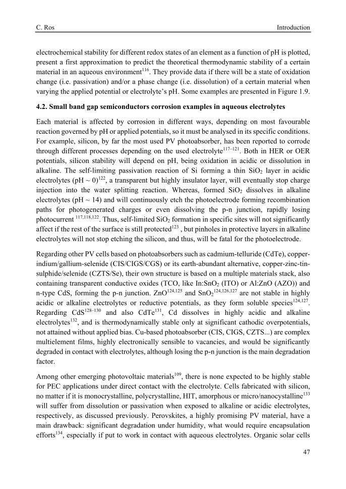
C. Ros Introduction
47
electrochemical stability for different redox states of an element as a function of pH is plotted, present a first approximation to predict the theoretical thermodynamic stability of a certain material in an aqueous environment116. They provide data if there will be a state of oxidation change (i.e. passivation) and/or a phase change (i.e. dissolution) of a certain material when varying the applied potential or electrolyte’s pH. Some examples are presented in Figure 1.9.
4.2. Small band gap semiconductors corrosion examples in aqueous electrolytes
Each material is affected by corrosion in different ways, depending on most favourable reaction governed by pH or applied potentials, so it must be analysed in its specific conditions. For example, silicon, by far the most used PV photoabsorber, has been reported to corrode through different processes depending on the used electrolyte117–121. Both in HER or OER potentials, silicon stability will depend on pH, being oxidation in acidic or dissolution in alkaline. The self-limiting passivation reaction of Si forming a thin SiO2 layer in acidic electrolytes (pH ~ 0)122, a transparent but highly insulator layer, will eventually stop charge injection into the water splitting reaction. Whereas, formed SiO2 dissolves in alkaline electrolytes (pH ~ 14) and will continuously etch the photoelectrode forming recombination paths for photogenerated charges or even dissolving the p-n junction, rapidly losing photocurrent 117,118,122. Thus, self-limited SiO2 formation in specific sites will not significantly affect if the rest of the surface is still protected123 , but pinholes in protective layers in alkaline electrolytes will not stop etching the silicon, and thus, will be fatal for the photoelectrode.
Regarding other PV cells based on photoabsorbers such as cadmium-telluride (CdTe), copper-indium/gallium-selenide (CIS/CIGS/CGS) or its earth-abundant alternative, copper-zinc-tin-sulphide/selenide (CZTS/Se), their own structure is based on a multiple materials stack, also containing transparent conductive oxides (TCO, like In:SnO2 (ITO) or Al:ZnO (AZO)) and n-type CdS, forming the p-n junction. ZnO124,125 and SnO2
124,126,127 are not stable in highly acidic or alkaline electrolytes or reductive potentials, as they form soluble species124,127. Regarding CdS128–130 and also CdTe131, Cd dissolves in highly acidic and alkaline electrolytes132, and is thermodynamically stable only at significant cathodic overpotentials, not attained without applied bias. Cu-based photoabsorber (CIS, CIGS, CZTS...) are complex multielement films, highly electronically sensible to vacancies, and would be significantly degraded in contact with electrolytes, although losing the p-n junction is the main degradation factor.
Among other emerging photovoltaic materials109, there is none expected to be highly stable for PEC applications under direct contact with the electrolyte. Cells fabricated with silicon, no matter if it is monocrystalline, polycrystalline, HIT, amorphous or micro/nanocystalline133 will suffer from dissolution or passivation when exposed to alkaline or acidic electrolytes, respectively, as discussed previously. Perovskites, a highly promising PV material, have a main drawback: significant degradation under humidity, what would require encapsulation efforts134, especially if put to work in contact with aqueous electrolytes. Organic solar cells

Chapter 1 C. Ros
48
have been implemented in PEC135 but require careful selection of redox couples, limiting their efficiency and pointing in stability problems. Dye sensitized solar cells (DSSC) or Grätzel cells, molecular dye decoration of a MOx framework as an intermediate to OER/HER catalyst presents significant instability of the molecular dye in the used potentials and electrolytes ranges. Thus, low productivities are expected136, or full cell encapsulation would be required, then further connected to the electrolyte with an external circuit, forming a PV-EC device configuration137.
C. Ros Introduction
49
5. Protective Layers to implement photovoltaic photoabsorbers into water splitting
Several strategies are possible to implement highly active photoabsorber materials into PEC water splitting avoiding their corrosion. Some authors have functionalized the surface of semiconductors with organic reagents like two-step chlorination/alkylation138 or by an alkylation through the halogenation/Grignard route139 to suppress corrosion, with relative success, but the majority of efforts have been put on depositing inorganic layers onto the photoabsorber to separate it from direct contact with the electrolyte93,140. Protective ultrathin layers of any material must consider even very slow dissolution rates (chemical or mechanical) for long-term operating devices, especially when considering flow systems and direct contact with gas bubbling.
These protective layers must allow electrical conduction, be thermodynamically stable, and optically transparent. M. F. Lichterman et al. stated all the properties under the acronym “SABOR”, meaning “Stable in the thermodynamic, kinetic, and mechanical senses when incorporated onto the semiconductor, immersed in the electrolyte, and operated at the potentials of interest; Active catalytically for the OER/HER, either possessing intrinsic catalytic activity or integrating the activity of a co-catalyst; capable of providing Built-in electronic asymmetry to allow for the separation of electrons and holes, or to allow for a separate buried junction to perform efficiently; Optically transparent to provide optical properties that are optimized for the transmission of light; and, capable of providing low Resistance, to allow for charge-carrier conduction with minimal performance loss due to iR drops” 141.
With protective layers incorporation, device’s complexity increases but photovoltage will now be governed by a solid-state junction rather than by the photoabsorber-electrolyte junction, increasing the possible materials candidates to be used. The extra layer can be used either to form an heterojunction, or to protect a buried junction. In addition, if the protective layer is not catalytic, an extra catalyst (layer or particles) must be added to reduce overpotentials. Although several interesting heterojunction strategies have been demonstrated for PEC water splitting electrodes with more or less success, focus will be put on extracting maximum efficiency from the photoabsorbers, using these extra layers to protect the photovoltaic-like junctions and the different techniques to deposit them.
5.1. Thin film deposition techniques
Thin film technology has become one of the main fields of study last decades, from basic sciences to industrial processes. Controlling material deposition at the nanoscale opens a whole new world of possibilities by combining physical and chemical properties from single or multiple element materials with overcoming intrinsic limitations due to phenomena only happening at the nanoscale142. For example, titanium dioxide, a wide band gap metal oxide,
Chapter 1 C. Ros
50
considered insulator at the macroscale, is conductive at the nanoscale; or metals, highly visible-light reflective and absorptive, can be turned into transparent if deposited few nanometers thick. There are a large amount of deposition techniques and variations among them for diverse applications, but some of the most used ones for inorganic thin film protective layers have been selected.
There are many non-vacuum liquid and chemical-based thin film deposition techniques, but not all of them are used to synthesize protective layers for different reasons. Among the liquid-based thin film deposition techniques, dip coating, spin coating or chemical bath deposition (CBD)143 are the more used ones, but require direct contact of the (maybe) sensible photoabsorber with a liquid, which can alter its superficial chemical state and thus, performance. In addition, liquid-based techniques normally produce either porous, not homogeneous at the nanoscale or abundant-pinhole films compared to vacuum technologies, and to eliminate precursor residues or crystallize them they require thermal post-treatments, which can create cracks in the protective layer or affect the photoabsorber. For example, solution-deposited TiO2 by spin-casting or spray pyrolysis presented significant pinholes, allowing electrolyte to penetrate and dissolve the photoabsorber, being fatal for the device even with 80 nm thick layers144.
Electroplating is one of the oldest techniques to form metallic thin films since the 19th century. Generally known as electrochemical deposition145, a conductive substrate (in our case, the photoabsorber) is introduced in an electrolyte containing the desired thin film precursor ions and, under controlled polarization, a redox reaction occurs, forming a film of electrodeposited material in the surface of the electrode (Figure 1.10a). It can be extended to any material capable to be deposited in a certain potential window that will depend on the electrolyte media, and is very interesting thanks to its easiness and the wide range of materials possible to be deposited, from metals to metal oxides and sulphides, even with nanoscale morphology control. It requires no vacuum, usually it is carried out at room or moderate temperatures, and with affordable infrastructure, like a power supply, lab equipment and the precursor materials. As drawbacks, it is highly depending on the substrate, that needs to be conductive, and has a moderate throwing power (the capacity to deposit an uniform film over an irregular substrate), not suitable for nanostructured substrates where a high aspect ratio is required. In some cases, nucleation promote the formation of particles rather than a layer, such as electrodeposited Ni oxide/hydroxide, a transparent, chemically resistant and catalytic material, that forms porous layers16,146, not isolating the substrate from electrolyte, whereas NiO deposited by sputtering creates a solid impermeable layer147. Also, the substrate will be in direct contact with the electrolyte and its properties can be affected. Many works have used electrochemical techniques to deposit catalytic particles or films to enhance OER or HER kinetics on already previously protected semiconductors148.

C. Ros Introduction
51
Figure 1.10. Representative schemes of thin film deposition techniques by a) electrochemical deposition, b) thermal evaporation and d) sputtering.
Vacuum technologies allow for an inert and controlled atmosphere deposition, favourable for more homogeneous deposited films and process-control143. Among the physical vapour deposition (PVD) techniques, thermal evaporation is one of the simplest, where a crucible is heated to high temperatures, vaporizing the materials contained143,149. Evaporated particles will travel and solidify forming a film on top of a substrate (Figure 1.10b). However, as different elements vaporize at different temperatures, the technique is useful for single element metals but has reduced stoichiometry reproducibility for mixes elements. Evaporated metallic films have been used as intermediate, protective or catalytic layers in water splitting. Sputtering deposition150,151 is based on an inert gas (i.e. argon) being ionized and accelerated towards a blank, impacting with high energies and removing particles which will travel until being deposited in our substrate (Figure 1.10c). Direct current (DC) sputtering is useful for conductive blanks (materials to be deposited), and radio-frequency (RF) sputtering allows insulator materials deposition. In reactive sputtering, other gases can be introduced at low pressures in the chamber, reacting with the traveling particles before being deposited (i.e. the oxygen presence can be controlled to tune metal oxides stoichiometry and with this, electrical, optical or other characteristics). Sputtering has been widely used to deposit catalysts152 and protective layers, thanks to the material possibilities, among them stoichiometry-controlled oxides such as TiO2
153,154 or NiO147 and no dependence on used substrate. Some authors have
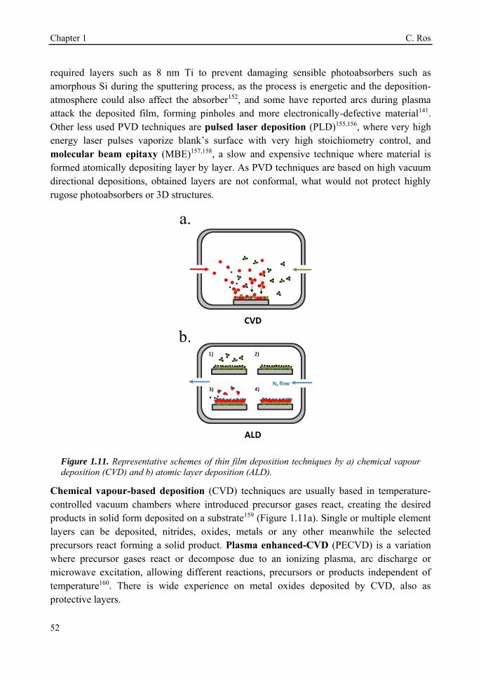
Chapter 1 C. Ros
52
required layers such as 8 nm Ti to prevent damaging sensible photoabsorbers such as amorphous Si during the sputtering process, as the process is energetic and the deposition-atmosphere could also affect the absorber152, and some have reported arcs during plasma attack the deposited film, forming pinholes and more electronically-defective material141. Other less used PVD techniques are pulsed laser deposition (PLD)155,156, where very high energy laser pulses vaporize blank’s surface with very high stoichiometry control, and molecular beam epitaxy (MBE)157,158, a slow and expensive technique where material is formed atomically depositing layer by layer. As PVD techniques are based on high vacuum directional depositions, obtained layers are not conformal, what would not protect highly rugose photoabsorbers or 3D structures.
Figure 1.11. Representative schemes of thin film deposition techniques by a) chemical vapour deposition (CVD) and b) atomic layer deposition (ALD).
Chemical vapour-based deposition (CVD) techniques are usually based in temperature-controlled vacuum chambers where introduced precursor gases react, creating the desired products in solid form deposited on a substrate159 (Figure 1.11a). Single or multiple element layers can be deposited, nitrides, oxides, metals or any other meanwhile the selected precursors react forming a solid product. Plasma enhanced-CVD (PECVD) is a variation where precursor gases react or decompose due to an ionizing plasma, arc discharge or microwave excitation, allowing different reactions, precursors or products independent of temperature160. There is wide experience on metal oxides deposited by CVD, also as protective layers.
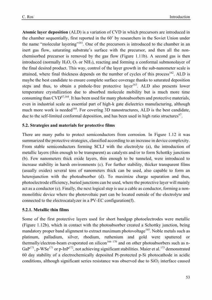
C. Ros Introduction
53
Atomic layer deposition (ALD) is a variation of CVD in which precursors are introduced in the chamber sequentially, first reported in the 60’ by researchers in the Soviet Union under the name “molecular layering”161. One of the precursors is introduced to the chamber in an inert gas flow, saturating substrate’s surface with the precursor, and then all the non-chemisorbed precursor is removed by the gas flow (Figure 1.11b). A second gas is then introduced (normally H2O, O3 or NH3), reacting and forming a conformal submonolayer of the final desired product. This way, control of the layer growth in the sub-nanometer scale is attained, where final thickness depends on the number of cycles of this process162. ALD is maybe the best candidate to ensure complete surface coverage thanks to saturated deposition steps and thus, to obtain a pinhole-free protective layer163. ALD also presents lower temperature crystallization due to absorbed molecule mobility but is much more time consuming than CVD67,164. It has been used for many photoabsorbers and protective materials, even in industrial scale as essential part of high-k gate dielectrics manufacturing, although much more work is needed164. For covering 3D nanostructures, ALD is the best candidate, due to the self-limited conformal deposition, and has been used in high ratio structures67.
5.2. Strategies and materials for protective films
There are many paths to protect semiconductors from corrosion. In Figure 1.12 it was summarized the protective strategies, classified according to an increase in device complexity. From stable semiconductors forming SCLJ with the electrolyte (a), the introduction of metallic layers (thin enough to be transparent) as catalysts and/or to form Schottky junctions (b). Few nanometers thick oxide layers, thin enough to be tunneled, were introduced to increase stability in harsh environments (c). For further stability, thicker transparent films (usually oxides) several tens of nanometers thick can be used, also capable to form an heterojunction with the photoabsorber (d). To maximize charge separation and thus, photoelectrode efficiency, buried junctions can be used, where the protective layer will mainly act as a conductor (e). Finally, the next logical step is use a cable as conductor, forming a non-monolithic device where the photovoltaic part can be located outside of the electrolyte and connected to the electrocatalyzer in a PV-EC configuration(f).
5.2.1. Metallic thin films
Some of the first protective layers used for short bandgap photoelectrodes were metallic (Figure 1.12b), which in contact with the photoabsorber created a Schottky junction, being mandatory proper band alignment to extract maximum photovoltage165. Noble metals such as platinum, palladium, silver, rhodium, ruthenium and gold were sputtered or thermally/electron-beam evaporated on silicon166–170 and on other photoabsorbers such as n-GaP171, p-WSe171 or p-InP172, not achieving significant stabilities. Maier et al.173 demonstrated 60 day stability of a electrochemically deposited Pt-protected p-Si photocathode in acidic conditions, although significant series resistance was observed due to SiO2 interface caused
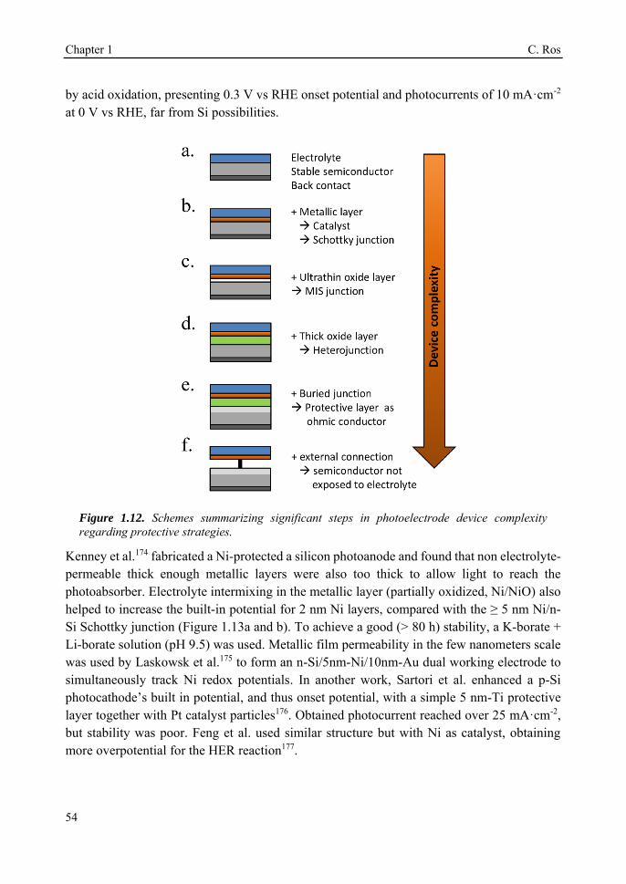
Chapter 1 C. Ros
54
by acid oxidation, presenting 0.3 V vs RHE onset potential and photocurrents of 10 mA·cm-2 at 0 V vs RHE, far from Si possibilities.
Figure 1.12. Schemes summarizing significant steps in photoelectrode device complexity regarding protective strategies.
Kenney et al.174 fabricated a Ni-protected a silicon photoanode and found that non electrolyte-permeable thick enough metallic layers were also too thick to allow light to reach the photoabsorber. Electrolyte intermixing in the metallic layer (partially oxidized, Ni/NiO) also helped to increase the built-in potential for 2 nm Ni layers, compared with the ≥ 5 nm Ni/n-Si Schottky junction (Figure 1.13a and b). To achieve a good (> 80 h) stability, a K-borate + Li-borate solution (pH 9.5) was used. Metallic film permeability in the few nanometers scale was used by Laskowsk et al.175 to form an n-Si/5nm-Ni/10nm-Au dual working electrode to simultaneously track Ni redox potentials. In another work, Sartori et al. enhanced a p-Si photocathode’s built in potential, and thus onset potential, with a simple 5 nm-Ti protective layer together with Pt catalyst particles176. Obtained photocurrent reached over 25 mA·cm-2, but stability was poor. Feng et al. used similar structure but with Ni as catalyst, obtaining more overpotential for the HER reaction177.

C. Ros Introduction
55
Figure 1.13. a) Scheme of n-Si photoanodes protected and catalysed by few nanometer-thick Ni films, demonstrating the effect of extremely thin layers compared to thicker ones. Reproduced from Kenney et al.174 b) Cyclic voltammogram response of the same Ni-protected silicon photoanodes with different Ni thicknesses, presenting higher photopotential for ~2 nm films and light absorption if thicker than 10 nm. c) Scheme showing photogenerated charges being collected by the depletion formed between a semiconductor and metallic isles embedded in an insulator transparent protective layer. Reproduced from Lewerenz et at.123
Although interesting results have been obtained with a metallic protective layer, the full potential of the photoabsorbers in long-term stabilities cannot be exploited due to insufficient

Chapter 1 C. Ros
56
stability, significant light absorption in the metallic layer and significant recombination in the Schottky junction due to extra states in the interface and Fermi level pinning, lowering photovoltage178.
To overcome metallic film transparency limitations, some works have proposed microstructured surfaces, with Pt islands (~30 nm thick) in contact with p-Si, and SiO2 covering the rest of the surface, in a balance between surface coverage of catalytic metal and oxide-protected light absorption regions123 (Figure 1.13c).
Regarding the limitations of metal-photoabsorber Schottky junctions, Seger et. al.179 proposed a buried silicon p-n homojunction in 2012 to maximize electron-hole separation, with a thin Ti metallic film which partially oxidized to TiO2 in the acidic electrolyte and using MoS2 as catalyst. This way, up to 16 mA·cm-2 were obtained at 0.2 V vs RHE (with 0.6 V photovoltage) and 1 h stability. Similar buried junction structure was used by Mei et. al.180 using 2-6 nm Ir/IrOx as protective layer in acidic electrolyte, avoiding detrimental SiOx formation.
5.2.2. Tunnel-thick protective films
Insulator thin films (Figure 1.12c), mainly oxides, have been studied to protect water splitting photoelectrodes thanks to their chemical stability. However, the system must still be capable to inject the photogenerated charges across the insulator layer and into the electrolyte to perform the water splitting reaction efficiently. For that, tunnelling-distance-thick films in the few nanometers scale have been combined with catalytic films or particles, forming a metal-insulator-semiconductor (MIS) or semiconductor-insulator-semiconductor (SIS) scheme. Advantages of these structures are the passivation of photoabsorber surface states and the suppression of Fermi level pinning181,182, but insulator oxides must be maintained under 3 nm thick to avoid significant tunnelling resistances161. ALD allows the fabrication of ultrathin conformal oxides, expected to be pinhole-free183.
Silicon dioxide (SiO2) was first studied due to its natural occurrence when Si is exposed to acidic electrolytes on a n-Si/SiO2/Pt photoanode, with poor results184. Esposito et al.185 fabricated a 2 nm thick SiO2 protected MIS photocathode by controlling the oxidation with rapid thermal oxidation (RTO) and depositing 30/20 nm Ti/Pt islands. Pt was used as HER catalyst, but Ti, with lower work function, enhanced photovoltage and also served as adhesion layer. Although 20/30 nm metallic islands are not transparent, controlling the pitch distance and diameter they could maximize light absorption and catalysis up to photocurrents of 20 mA·cm-2 at 0 V vs RHE and 0.55 V vs RHE onset potential in 0.5 M H2SO4, with reported 2 h stability.
n-type silicon photoanodes were fabricated with SiO2 and Ir as catalyst with photovoltages exceeding 500 mV and saturation photocurrents about 30 mA·cm-2, although an ultrathin TiO2 protective layer was needed to stop rapid further Si oxidation at oxidative potentials and

C. Ros Introduction
57
stabilize for over 8 h the photoanodes in acidic, neutral or basic media183,186 (Figure 1.14a and b). Planar and nanopilar p-InP was 3 nm n-TiO2-protected and 2 nm Ru film was added as catalyst, achieving significant photocurrents of 35 mA·cm-2 stable for some hours and 0.75 V vs NHE onset potentials187. Photoanodes without the TiO2 degraded rapidly during the first hour. In this scheme, increasing TiO2 layer thickness turned into lower trap-mediated thickness-dependent conductivity indicating the importance of using a thin TiO2 layer for efficient tunnelling-mediated electron transport183,188–190. 490 mV photovoltage was also obtained substituting ultrathin TiO2 by Al2O3, finding that tunnelling layers of a thickness > 2 nm introduce an intermediate resistance, lower than insulator SiO2 but higher than defect-conductive TiO2
191,192. Crystalline TiO2 was found to reduce insulator-thickness-dependent photovoltage loss in metal-insulator-semiconductor (MIS) type photoanodes, in comparison with amorphous TiO2 (ALD-fabricated at 170 ºC), due to dielectric constant increase, with a record photovoltage of 623 mV193. TiO2 was proven as one of the best candidates, highly protective, and has been identified to be conductive for thicker than 10 nm layers, where tunnelling is highly non-probable. Indeed, hopping via trap states situated ~1 eV below the conduction band was considered the conduction mechanism in photoanode’s case194, following Campet et al “defect band” first proposed conductivity195, and will be further discussed in the next section together with other thicker conductive oxides protective layers.
Ultrathin oxides, like metallic thin films, are difficult to fabricate being impermeable and pinhole-free for devices lasting hundreds of hours, and majority of the presented works lack long-term stabilities and device fail mechanisms over large device’s area.
5.2.3. Conductive transparent oxides and other protective films
Increasing the protective layers thickness (Figure 1.12d and e) can overcome the stability limitations present in ultrathin metallic or insulating coatings, by avoiding possible electrolyte permeability or reducing pinholes and cracks probability. For films thicker than 5 nm, tunnelling conductivity is not possible, thus material electronic properties (interfacial potential barriers, band alignment, charge mobility, band bending, etc) must be taken into account, in addition to chemical stability (as explained in section 4). Also, protective layers must be intrinsically transparent and conductive, reducing candidates to mid band gap (2-5 eV) semiconductors, transparent to significant part of the visible spectra while not being insulator materials, such as Al2O3 and SiO2 (Eg > 9 eV). Luckily the majority of metal oxides studied for protective layers are earth abundant and non-toxic as needed for device scalability196.
For an efficient conductivity through protection layers, minimal losses in bulk resistance and semiconductor-electrolyte interface must be attained. The protective layers do not need to be as conductive as conventional transparent conductive oxides as only vertical (some tens of nanometers) conductivity is needed, not in-plane several hundred microns as in solar cells. In general, n-type metal oxide semiconductors have been used to protect photocathodes, based

Chapter 1 C. Ros
58
on electrons migrating from the photoabsorber, through the protective layer, and injected in the HER. Fermi level close to the conduction band should help both to form a p-n heterojunction and for favourable alignment with the n-type part of the p-n buried junction. Likewise, p-type semiconductors have been proposed for photoanodes and have efficient OER catalytic surfaces97,148,196,197. The role of cocatalysts on top of the protective layer and the electrolyte is majorly governed by the pinch-off effect, where with few nanometers thick layers, cocatalysts do not really form a Schottky barrier, and rather what is called “adaptive junctions”198. Although, material specificities and the formation of recombining contacts have made materials such as TiO2 highly versatile, multiple strategies are possible controlling deposition conditions, oxygen stoichiometry and other metals incorporation for better conductivity or catalysis190. Transparent and conductive oxides used in the microelectronics industry, such as ITO and AZO, were expected to have good band offsets and conductivity, but their stability and performance resulted very poor195,199. With thick oxides protective layers such as TiO2, NiO, CoOx and MnO, among others, better results have been achieved in terms of productivity and stability, with tens of mA·cm-2, minimal resistances introduced and several hundred hours, even thousands, of operation tests.
a) TiO2
Titanium dioxide has been one of the most studied materials as protective layer for small band gap photoelectrodes thanks to its transmittance, relatively good electrical properties and chemical stability. It is an earth abundant metal oxide found in nature and with several fabrication routes, such as anodization, hydrothermal, sol-gel and, for protective layers, mostly known to be fabricated by sputtering and ALD, giving compact layers in comparison with other solution-deposited ones144. TiO2 is a n-type semiconductor with ~3.2 eV band gap153,200, permitting almost complete optical transmittance for visible light spectra, although thanks to its good chemical stability some works have used it also for back-illuminated photoelectrodes201. Its n-type semiconductor behaviour is known to be caused by oxygen vacancies and thus, Ti3+ states with energy levels close to the conduction band, giving free electrons. TiO2 is known to have significant oxygen mobility under polarization or under different atmospheres annealing, locally forming conductive filaments acting as degenerate n-type material across the whole layer, explaining various mechanisms reported depending on fabrication and working conditions161.

C. Ros Introduction
59
Figure 1.14. a) TEM image of an ultrathin ALD-TiO2 + SiO2 protective layer for a silicon photoanode. b) Equivalent energy band diagram under illumination. Reproduced from Chen et al.183 c) Energy band diagram of a 5 nm Ti/100 nm-TiO2 protected silicon photocathode having a buried p-n junction under illumination. Reproduced from Seger et al.202 d) SEM images of a <100> Si TiO2-protected and unprotected after immersion in 1 M KOH for 3 days. e) Schematics of the anisotropic etching process forming characteristic inversed pyramids. Reproduced from Bae et al.122.

Chapter 1 C. Ros
60
Photocathodic protection with thick (~100 nm) sputtered TiO2 was first reported in 2013 by Seger et al.202 in a pn+-Si/(5 nm)Ti/(100 nm)TiO2/Pt structure, where favourable band alignment between n+-Si, Ti/TiO2 and TiO2/Pt interface (behaving like an ohmic contact due to high dopant density of TiO2 and high energy sputtered Pt, rather than like a Schottky junction203,204) introduced negligible resistance or overpotential (Figure 1.14c). These findings show the system acting equivalently to a solar cell in series with the catalyst metal. They demonstrated conductivity through the conduction band, also explained to be electron polaron hopping through the Ti3+ states close to the conduction band (~0.3 eV)205, although the transition temperature between both mechanisms is reported to be about 300 K (room temperature)206 and probably both mechanisms are simultaneously active. Seger et al. introduced a 5 nm Ti layer previous to TiO2 reactive-sputtering deposition to prevent Si substrate from oxidation, a strategy followed by other works122,153,201,207 based on oxygen migration to lowest Gibbs oxide formation energy and thus, oxygen scavenging from Si to Ti208,209. Up to 20 mA·cm-2 at 0.3 V vs RHE and 70 h of stability were obtained under illumination, corroborating the photoabsorber-protective layer strategy. In following works, durability was studied, reporting the need of 400 ºC post-annealing to ALD-TiO2 protective layers synthetized at 200 ºC to reach from 8 to 480 h of stability at 0.3 V vs RHE in 1 M HClO4
210. An increase of doping level under the 400 ºC annealing was considered to be the reason of significantly higher conductivity, reducing depletion barrier between the TiO2 and electrolyte, allowing electrons to tunnel through211, in similar results to Liang et al.212 increasing donor level by hydrogen doping upon deposition. Deposition techniques such as high power impulse magnetron sputtering (HPIMS)122 have been used to increase layer’s density and thus, minimizing pinholes to avoid electrolyte penetration and anisotropic etch corrosion by KOH (Figure 1.14d and e). TiO2 conduction band is close to the HER potential, and with sufficient dopant levels (i.e. oxygen vacancies), electrons can overcome by tunnelling the small potential barrier formed and reach the catalyst202. Platinum, an expensive noble metal, has been widely used due to its superior cost-efficiency trade-off, and some works have demonstrated the scalability of very small amounts of platinum nanoparticles to drive the PEC water splitting industry to the terawatt level213.
Regarding photoanodes, although TiO2 should not be expected to be a good hole-conduction layer, in 2014, Hu et al.194 discovered that depositing amorphous TiO2 on Si, GaAs, and GaP conduction was possible for films up to 143 nm thick (grown by ALD at 150 ºC and Ni coated). Energy states about 1 eV inside the forbidden band were observed by high resolution XPS (Figure 1.15a). Conductivity through intra-band gap levels was also explained by K. Sivula as “Leaky titania” (Figure 1.15b)214, based on the concept theorized by Campet et al. time ago195, and following works performed thoughtful energy band calculations to explain it154,215. Deeper studies are necessary, as weak traces of anatase have been reported down to 140 ºC216. McDowell et al.154 found TiO2 films conduction behaviour not unique to amorphous phase (Figure 1.15c) and with no relation to carbon or nitrogen impurities, although high
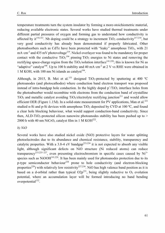
C. Ros Introduction
61
temperature treatments turn the system insulator by forming a more-stoichiometric material, reducing available electronic states. Several works have studied thermal treatments under different partial pressures of oxygen and forming gas to understand how conductivity is affected by it154,161. Nb doping could be a strategy to increment TiO2 conductivity217,218, but very good conductivity has already been demonstrated if properly fabricated. Other photoabsorbers such as CdTe have been protected with “leaky” amorphous TiO2, with 21 mA·cm-2 and 435 mV photovoltage219. Nickel overlayer was found to be mandatory for proper contact with the conductive TiO2
194, pinning TiO2 energies to Ni states and removing the
rectifying space-charge region from the TiO2/solution interface141,220; this is known for Ni as “adaptive” catalyst198. Up to 100 h stability and 40 mA·cm-2 at 2 V vs RHE were obtained in 1 M KOH, with 100 nm Ni islands as catalyst194.
Although, in 2015, B. Mei et al.153 designed TiO2-protected by sputtering at 400 ºC photoanodes (and photocathodes) where conduction band electron transport was proposed instead of intra-bandgap hole conduction. In the highly doped p+/TiO2 interface holes from the photoabsorber would recombine with electrons from the conduction band of crystalline TiO2 and metallic catalyst avoiding TiO2/electrolyte rectifying junction211 and would allow efficient OER (Figure 1.15d). In a solid-state measurement for PV applications, Man et al.221 studied n-Si and p-Si devices with amorphous TiO2 deposited by CVD at 100 ºC, and found a clear hole blocking behaviour, what would support conduction-band conductivity. Since then, ALD-TiO2-protected silicon nanowire photoanodes stability has been pushed up to > 2000 h with 40 nm NiCrOx catalyst film in 1 M KOH222.
b) NiO
Several works have also studied nickel oxide (NiO) protective layers for water splitting photoelectrodes due to its abundance and chemical resistance, stability, transparency and catalytic properties. With a 3.8-4 eV bandgap223,224 it is not expected to absorb any visible light, although significant defects on NiO structure (Ni reduced atoms) can reduce transparency215,225–227, even presenting electrochromism in specific cases caused by Ni3+ species such as NiOOH141,226. It has been mainly used for photoanodes protection due to its p-type semiconductor behaviour228 prone to hole conductivity (and electron-blocking properties229) with relatively low resistivity227,230. NiO has high valence band position as it is based on a d-orbital rather than typical O2p231, being slightly reductive to O2 evolution potential, where an accumulation layer will be formed introducing no band bending overpotential132.
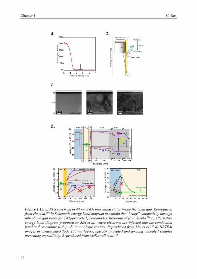
Chapter 1 C. Ros
62
Figure 1.15. a) XPS spectrum of 44 nm-TiO2 presenting states inside the band gap. Reproduced from Hu et al.194 b) Schematic energy band diagram to explain the “Leaky” conductivity through intra-band gap states for TiO2-protected photoanodes. Reproduced from Sivula.214 c) Alternative energy band diagram proposed by Mei et al. where electrons are injected into the conduction band and recombine with p+-Si in an ohmic contact. Reproduced from Mei et al.232 d) HRTEM images of as-deposited TiO2 100 nm layers, and Air annealed and forming annealed samples presenting crystallinity. Reproduced from McDowell et al.154
C. Ros Introduction
63
Although, few works have used it for photocathodes, i.e. a Cu2O electrode 10 nm-NiO protected233 with 70% retained current after 20 min in neutral pH, NiO is reduced in acidic electrolytes and cathodic HER potentials234. Its p-type semiconductivity is given by point defects and Ni2+ vacancies, and is explained by the Mott-Hubbard insulator theory132. The Ni2+ vacancies contribute with extra oxygen in the structure, which is compensated by oxidation of nickel sites to Ni3+ states, electron acceptors235–238. Changes in these favorable imperfections due to atomic reorganization caused by temperature treatments, oxygen partial pressure or different layer growth process are crucial in achieving a conductive layer (Figure 1.16a)132,224,227,235,239,240, with significant defects portion affecting on transparency. NiO films are known to present oxygen anions migration under polarization241, up to filament formation242, which must be taken in account as stoichiometry modifications can reduce or enhance conductivity.
Also, nickel is known to be one of the best earth-abundant OER catalysts in alkaline media243, where it is highly stable (but not in acid132). First trials on nickel-based protective layers were performed directly depositing metallic Ni on top of the photoelectrode and letting it oxidize in contact with the electrolyte, but the hydroxide formed is highly porous and permeable244–
246 after oxy-hydroxide species restructuration (migration) during initial operation243, hydrating up to 10 nm deep. Thicker Ni films, to protect the semiconductor beneath, would still contain a metallic layer, partially absorbing light and reducing photocurrent174.
First NiO protected silicon p-n junction was performed in 1987 presenting several high overpotential247. In 2014, Mei et al.248 used reactive sputtering to deposit 50 nm thick NiO layers on a buried np+-Si homojunction previously protected with 5 nm Ni, inactive to OER if no pre-treatment in Fe-containing electrolyte was performed (Figure 1.16b). This achieved over 300 h stability of silicon photoanodes in 1 M KOH with 14 mA·cm-2 at 1.3 V vs RHE. Soon after, Sun et al.147 reported 75 nm thick RF-sputtered NiO-protected photoanodes giving 30 mA·cm-2 at 1.73 V vs RHE over 1200 h (Figure 1.16c and d), where some defects attributed to arc-discharges during RF-sputtering were observed and partial oxygen pressure during synthesis is highly important in resulting conductivity224. III-V semiconductors such as InP could also be protected with the same kind of layers for over 48 h226 or CdTe, HTJ-Si or a-Si:H over 100 h224. Significant advance was obtained compared with previous attempts from 2012 with sol-gel NiO reaching ~1 mA·cm-2 and losing 50% of performance in 1 h 249 or 2013 NiRuOx sputtered to form an heterojunction with n-Si giving over 1 h stability with not much photovoltage118. ALD has only been used for NiO electroactive films few times250, with Ni(Cp)2 and O3 as precursors at 275 ºC deposition temperature. 3-18 nm thick films were found more resistive when ALD deposited than by other techniques together with the need of Fe atoms incorporation for sustained OER current (Figure 1.16e and f).
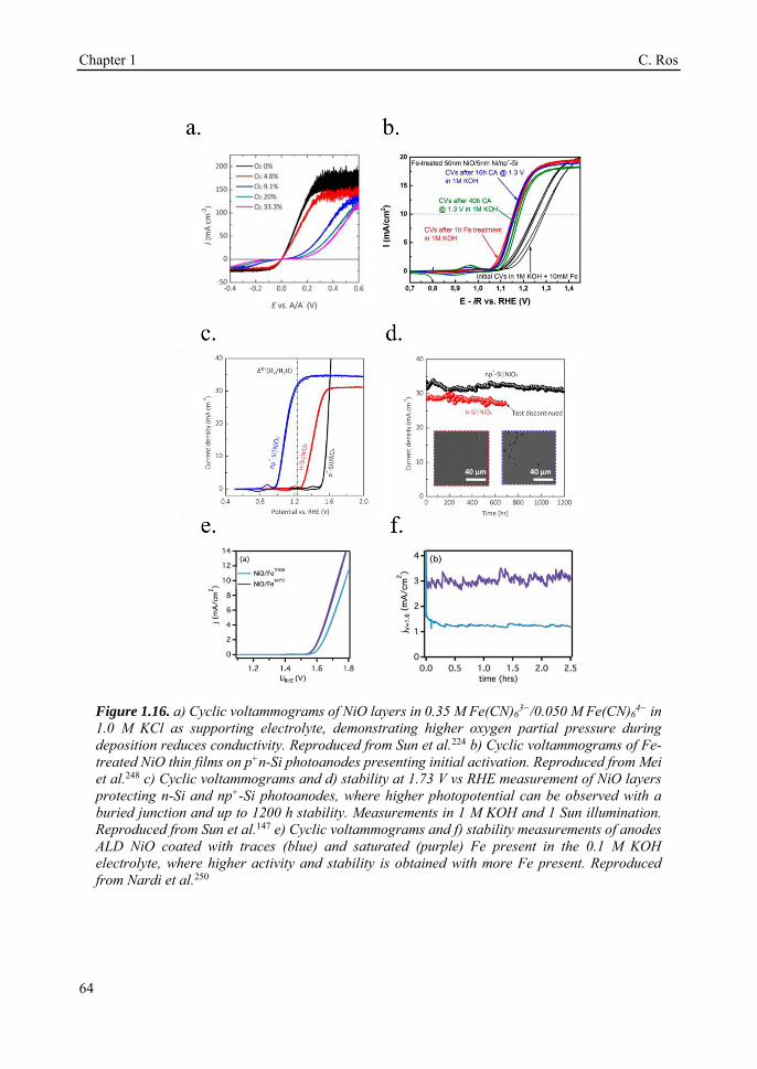
Chapter 1 C. Ros
64
Figure 1.16. a) Cyclic voltammograms of NiO layers in 0.35 M Fe(CN)63−/0.050 M Fe(CN)6
4− in 1.0 M KCl as supporting electrolyte, demonstrating higher oxygen partial pressure during deposition reduces conductivity. Reproduced from Sun et al.224 b) Cyclic voltammograms of Fe-treated NiO thin films on p+n-Si photoanodes presenting initial activation. Reproduced from Mei et al.248 c) Cyclic voltammograms and d) stability at 1.73 V vs RHE measurement of NiO layers protecting n-Si and np+-Si photoanodes, where higher photopotential can be observed with a buried junction and up to 1200 h stability. Measurements in 1 M KOH and 1 Sun illumination. Reproduced from Sun et al.147 e) Cyclic voltammograms and f) stability measurements of anodes ALD NiO coated with traces (blue) and saturated (purple) Fe present in the 0.1 M KOH electrolyte, where higher activity and stability is obtained with more Fe present. Reproduced from Nardi et al.250

C. Ros Introduction
65
Nickel-based electrocatalysts are known to be enhanced after cycling at positive potentials147, related to NiO hydration to NiOOH224 and incorporation of other metal traces, like Fe243,251,252 (with higher activated-state stability with higher amount of Fe incorporated250), Co243 and Ru118. The surface of nickel oxide is affected in its surface by alkaline electrolytes, forming oxy-hydroxides and porous nanoflakes with high surface area243,246 although it is stabilized by the presence of Co, partially inhibiting oxyhydroxide formation and restructuration243. These hydroxides (Ni(OH)2) and oxy-hydroxides (NiOOH), important in various fields of chemistry and physics244, are not expected to create significant potential barriers with NiO beneath due to the porous and adaptive junction thanks to abundant electronic states and electrolyte penetration on first nanometers198,253. Also, it is known to be the responsible of the efficient OER catalysis.
c) CoOx
Cobalt oxide (CoOx) is a metal oxide similar to NiO in many aspects. With p-type semiconductor behaviour and high conduction band edge, it is favourable to hole conductivity and as electron blocking layer132. It is expected to be transparent to large part of visible spectra due to its ~2.3 eV band gap254,255. It is hydroxylated in contact with alkaline media into CoOOH, a known stable and active catalyst for O2 evolution (OER)256, forming nanosheet/nanoflake structures257,258 (Figure 1.17a). Its OER catalysis is highly enhanced by fabricating it already containing Fe258 or incorporating Fe from the electrolyte258 with low overpotentials (~250 mV @ 10 mA·cm-2), close to NiFe257. Depositing few nanometers ALD CoOx on np+-Si photoanodes up to 30 mA·cm-2 were obtained by Yang et at al at 1.4 V vs RHE in 1 M NaOH and 1 sun illumination stable for 24 h259.
Bae et al.254 sputter-deposited 50 nm thick NiCoOx protective layers on back-illuminated photoanodes, reaching stabilities over 72 h and 22 mA·cm-2 at 1.23 V vs RHE at pH 14 and further enhanced by Fe traces incorporation from the electrolyte. Xing et al.260 co-sputtered CoOx with 3-8% vanadium 70 nm thick layers on 2 nm Cr protected p+n-Si textured photoanodes, with almost 30 mA·cm-2 at 1.23 V vs RHE. Zhou et al.261 CoOx protected by ALD an n-silicon photoanode containing a thin SiO2 layer to form a SIS heterojunction, reaching 570 mV photovoltage and 30 mA·cm-2 at 1.23 V vs RHE and stable for up to 2500 h at 1.63 V vs RHE in 1 M KOH (Figure 1.17b, c and d). Burke et al.258 cathodically electrodeposited Co1-xFex(OH)2 ~50 nm thick finding that the incorporation of Fe reduced up to 100 times OER overpotential compared to pure CoOOH thanks to strong Co-Fe coupling up to 60% Fe, but at higher amounts, conductivity was reduced and the layer dissolved as FeOOH is soluble in basic mediums unless incorporated in NiOOH or CoOOH. This would suggest CoOOH acts as “conductive, chemically stable, and intrinsically porous/electrolyte-permeable host for Fe, which substitutes Co atoms and serves as the (most) active site for OER catalysis”. Other metals such as Ru or Rh have been combined with CoOx to further reduce its OER262. Tung et al.256 found one of the causes of long-term instability is volume

Chapter 1 C. Ros
66
expansion on phase change due to hydroxylation to CoOOH, and thus, nanoscale structuration can prevent detachment and efficiency loss.
Figure 1.17. a) SEM image of Co(OH)2 electrodeposited for 2 min. Reproduced from Jiang et al.257 b) High resolution cross section TEM images of polycrystalline CoOx-protected n-Si photoelectrode. c) Stability measurement at 1.63 V vs RHE and d) cyclic voltammogram of the CoOx-Protected n-Si photoelectrode under 1.1 sun illumination in 1 M KOH. Reproduced from Zhou et al.261
d) Other conductive protective layers
Back in 1987, Kainthla et al.263 protected n-Si with MnO achieving stable photoanode for 650 h giving 1 mA·cm-2 at 1.3 V vs NHE in 0.5 M K2SO4 solution. In 2012, up to 20 nm ALD MnO films were used by Strandwitz et al.117 to protect n-Si and obtained almost 30 mA·cm-2
at 1.5 V vs RHE in 1 M KOH and 550 mV photovoltage, but not stable for more than 10 min. They also found film thickness increase introduced significant resistance, affecting fill factor.
Transparent and conductive thallium oxide (Tl2O3) was deposited 3-4 µm thick by Switzer et al.264 protecting an n-Si photoanode. A SIS junction was formed, with over 500 mV photovoltage and 33 mA·cm-2 photocurrent with a Fe(CN)6
3+/4+ redox couple, although thallium is an expensive material with quite low abundance265.
~100 nm sputtered n-type Nb2O5 formed an heterojunction with p-type GaP in a work by Malizia et al.266, achieving 710 mV photovoltage, although its stability was found less than TiO2 protective layers in 1 M HClO4 attributed to Nb2O5 detachment and thus, Pt cocatalyst loss (Figure 1.18a). Avoiding pinholes corroding photoabsorber beneath is important, as some
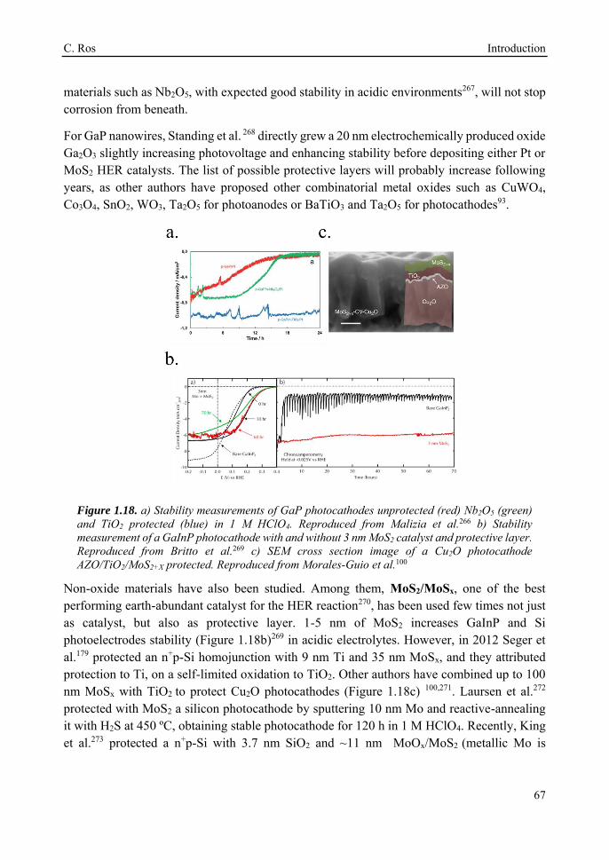
C. Ros Introduction
67
materials such as Nb2O5, with expected good stability in acidic environments267, will not stop corrosion from beneath.
For GaP nanowires, Standing et al. 268 directly grew a 20 nm electrochemically produced oxide Ga2O3 slightly increasing photovoltage and enhancing stability before depositing either Pt or MoS2 HER catalysts. The list of possible protective layers will probably increase following years, as other authors have proposed other combinatorial metal oxides such as CuWO4, Co3O4, SnO2, WO3, Ta2O5 for photoanodes or BaTiO3 and Ta2O5 for photocathodes93.
Figure 1.18. a) Stability measurements of GaP photocathodes unprotected (red) Nb2O5 (green) and TiO2 protected (blue) in 1 M HClO4. Reproduced from Malizia et al.266 b) Stability measurement of a GaInP photocathode with and without 3 nm MoS2 catalyst and protective layer. Reproduced from Britto et al.269 c) SEM cross section image of a Cu2O photocathode AZO/TiO2/MoS2+X protected. Reproduced from Morales-Guio et al.100
Non-oxide materials have also been studied. Among them, MoS2/MoSx, one of the best performing earth-abundant catalyst for the HER reaction270, has been used few times not just as catalyst, but also as protective layer. 1-5 nm of MoS2 increases GaInP and Si photoelectrodes stability (Figure 1.18b)269 in acidic electrolytes. However, in 2012 Seger et al.179 protected an n+p-Si homojunction with 9 nm Ti and 35 nm MoSx, and they attributed protection to Ti, on a self-limited oxidation to TiO2. Other authors have combined up to 100 nm MoSx with TiO2 to protect Cu2O photocathodes (Figure 1.18c) 100,271. Laursen et al.272 protected with MoS2 a silicon photocathode by sputtering 10 nm Mo and reactive-annealing it with H2S at 450 ºC, obtaining stable photocathode for 120 h in 1 M HClO4. Recently, King et al.273 protected a n+p-Si with 3.7 nm SiO2 and ~11 nm MoOx/MoS2 (metallic Mo is

Chapter 1 C. Ros
68
sputtered and further H2S atmosphere annealed) achieving up to 62 days (1638 h) stability with > 10 mA·cm-2 photocurrent at 0 V vs RHE in 0.5 M H2SO4.
C. Ros Introduction
69
6. Heterojunctions with the protective layer
Creating effective short band gap photoelectrodes requires highly conductive, transparent, stable and kinetically efficient protective layers and catalysts, but also to maximize the photovoltage of the system. For sensible-to-corrosion photoabsorbers, the electrolyte will not be in contact with the photoabsorber due to the introduction of the protective layer in between and thus, a semiconductor-liquid junction (SCLJ) will not be present to create an electric field to separate and extract photogenerated charges.
Forming an electronic junction between two different materials (at least one of them a semiconductor) forms an heterojunction. In this case, the maximum photovoltage of the photoelectrode is governed by the electronic properties of protective layers, photoabsorbers and interfacial energetics. Introducing heterojunctions results in a more complex device (Figure 1.12b-d), meanwhile it opens the possibility for higher photovoltages thanks to a larger amount of candidates available. Among them, three types of heterojunctions are considered: Schottky junctions (formed between a metal and a semiconductor), metal-insulator-semiconductor (MIS) junctions and semiconductor-semiconductor heterojunctions (composed of different materials).
6.1. Schottky and MIS junctions
In section 5 has been analysed how thin (few nanometers) metallic films can protect a semiconductor from corrosion, forming a Schottky junction (Figure 1.12b). However with limited stability and with significant recombination rates and Fermi level pinning caused by states in the metal-semiconductor interface, limiting electron-hole pseudo-Fermi level separation and thus, the photovoltage178. Even so, selecting appropriate metals with work functions low for photoanodes and high for photocathodes is mandatory to obtain significant photocurrents and photovoltages165. Very small photovoltages are obtained from just directly depositing Pt or Ni on p-Si, meanwhile 200 mV more can be generated with a p-Si/5nmTi contact previous to Pt catalyst (Figure 1.19a)173,176 or Ni catalyst177 thanks to higher Schottky barrier created by the favourable work function of Ti.
Introducing few nanometers of insulator materials between the semiconductor and the metal film (Figure 1.12c), such as SiO2 or Al2O3
178,274, can passivate interfacial electronic states and enhance energy level separation in the heterojunction (forming a metal-insulator-semiconductor junction, MIS). Specifically, Al2O3 is favourable to unpin the Si Fermi level, giving extra built-in potential. Regarding selected metal, Pt has higher work function than Ni and increases photovoltage in n-Si photoanodes (Figure 1.19b)274. Laskowski et al.175 suggest high barrier regions are formed when Si is oxidized to SiO2 due to electrolyte (pH 9.8 K-borate buffer) permeability in very thin (~3-5 nm) Ni films, avoiding Ni/n-Si Fermi level pinning and thus, increasing photovoltage (Figure 1.19c and d).

Chapter 1 C. Ros
70
Following this, several works have focused on the passivation of Si surface states with ultrathin semiconductor layers (0-12 nm) such as TiO2, although the junction is formed between the metallic film on top and the silicon, and thicker intermediate layers will increase metal to semiconductor separation, reducing formed photovoltage189. SrTiO3 epitaxial films, MBE-deposited by Ji et al.275,276 on p-Si with patterned 50 nm Ti/Pt catalyst formed a stable (>35 h in 0.5 M H2SO4) and effective photocathode (35 mA·cm-2 at -0.4 V vs NHE, 450 mV photovoltage) when only few unit cells (4-6, ~1.6 nm) of the strontium titanate were deposited. The space-charge region is formed between the p-Si and metallic Ti, with lower work function than Pt, as it has a work function similar to p-Si, and would generate small photovoltage. Although, these insulator layers introduce significant tunnelling resistance if thicker than 3 nm161 and do not significantly increase stability to corrosion.
Figure 1.19. a) Cyclic voltammogram of p-Si photoanodes where higher photovoltages can be observed if 5 nm Ti is used to form the Schottky junction and Pt on top as HER catalyst. Reproduced from Sartori et al.176 b) Cyclic voltammograms of n-Si photoanodes presenting higher MIS photovoltage if Al2O3 is used as ultrathin insulator layer and Pt as the metal intervening thanks to its work function, together with Ni as OER electrocatalyst. Reproduced from Digdaya et al.274 c) Cyclic voltammogram and d) scheme depicting the formation of adventitious interfacial ultrathin SiO2 preventing Fermi level pinning due to electrolyte (pH 9.8 K-borate buffer) penetration, and thus, forming higher photovoltage. Reproduced from Laskowski et al.175

C. Ros Introduction
71
6.2. Semiconductor–semiconductor heterojunctions with thick oxides
Similar schemes can be formed with thicker conductive oxides semiconductors instead of metals (Figure 1.12d), overcoming metal films limitations on thickness and transparency. In this case, heterojunctions between two semiconductor materials will be formed, where a thin insulator film can be introduced in the interface avoiding Fermi level pinning if necessary (forming a semiconductor-insulator-semiconductor (SIS) junction). Similar electronic structure to section 3.6 will be formed, but doing so with a short band gap material and a wide band gap metal oxide has a great benefit: the major part of photon absorption will occur in the short band gap one, collecting large portion of the visible spectra. Also, short band gap materials such as Si, GaAs or CIGS are very good photoabsorbers, with minimal recombination and transport losses.
Thicker-than-tunnelling metal oxides have been widely used both to protect short band gap semiconductors and to generate a built-in electric field. N-type wide band-gap semiconductors such as ZnO, WO3 or TiO2 have favourable energetics to form a heterojunction with p-type photoabsorbers such as Si, InP or CIGS in a similar strategy to SIS solar cells277. In 1996, Yoon et al. tested a different thickness n-type WO3 on p-Si, achieving a better photovoltage by controlling resistivity, carrier concentration and surface band bending (Figure 1.20a)278. In 1998279 they electron-beam evaporated 50 nm WO3 on top of p-Si with 1-2 nm Pt as catalyst, and the role of a more efficient built-in field is clearly observed when introducing WO3, with a better HER catalysis when Pt is incorporated (Figure 1.20b). Although, WO3 was found not to be stable if Pt was not blocking direct contact of WO3 with the acidic electrolyte (0.1 M H2SO4). By the introduction of an indium-doped tin oxide (ITO) layer, Coridan et al.280 demonstrated not such a good interface is formed between WO3 and Si, and the ITO layer could also act as an ohmic contact, allowing them to create a tandem cell. Wang et al.281 also demonstrated Fe2O3 heterojunction with n-Si and p-Si photoelectrodes.
Transparent conductive oxides (TCO) such as ITO and AZO were tested, as theoretically should be good conductive and transparent n-type semiconductors for photocathodes and thus, form good p-n heterojunctions. ZnO (~3.1 eV) was deposited by Sun et al. as a film and as nanorods on planar p-Si and nanowire-grown p-Si282, achieving better light absorption and active surface area thanks to the nanostructures and HER catalysis enhanced by Ni, Pt and Pd cocatalysts (Figure 1.20c). p-type Cu2O electrodes can also form an heterojunction with n-ZnO reaching more than 7 mA·cm-2, although TiO2 was required for higher stability even in 1 M Na2SO4 at reductive potentials77,100. Although, stability was limited to few minutes as ZnO is an amphoteric metal oxide unstable in alkaline and even more in acidic electrolytes283.
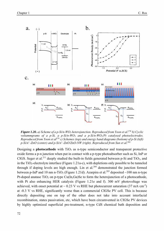
Chapter 1 C. Ros
72
Figure 1.20. a) Scheme of a p-Si/n-WO3 heterojunction. Reproduced from Yoon et al.278 b) Cyclic voltammgrams of a p-Si, a p-Si/n-WO3 and a p-Si/n-WO3/Pt catalysed photoelectrodes. Reproduced from Yoon et al279 c) Schemes (top) and energy band diagrams (bottom) of p-Si (left) p-Si/n+-ZnO (center) and p-Si/n+-ZnO/ZnO-NW (right). Reproduced from Sun et al.282
Designing a photocathode with TiO2 as n-type semiconductor and transparent protective oxide forms a p-n junction when put in contact with a p-type photoabsorber such as Si, InP or CIGS. Seger et al.211 deeply studied the built-in fields generated between p-Si and TiO2, and in the TiO2-electrolyte interface (Figure 1.21a-c), with depletions only possible to be tunneled through if doping levels are high enough. Lin et al.284 demonstrated the junction formed between p-InP and 10 nm n-TiO2 (Figure 1.21d). Azarpira et al.285 deposited ~100 nm n-type Pt-doped anatase TiO2 on p-type Cu(In,Ga)Se to form the heterojunction of a photocathode, with Pt also enhancing HER catalysis (Figure 1.21e and f). 300 mV photovoltage was achieved, with onset potential at ~ 0.23 V vs RHE but photocurrent saturation (37 mA·cm-2) at -0.3 V vs RHE, significantly worse than a commercial CIGSe PV cell. This is because directly depositing one on top of the other does not take into account interfacial recombination, states passivation, etc, which have been circumvented in CIGSe PV devices by highly optimized superficial pre-treatment, n-type CdS chemical bath deposition and
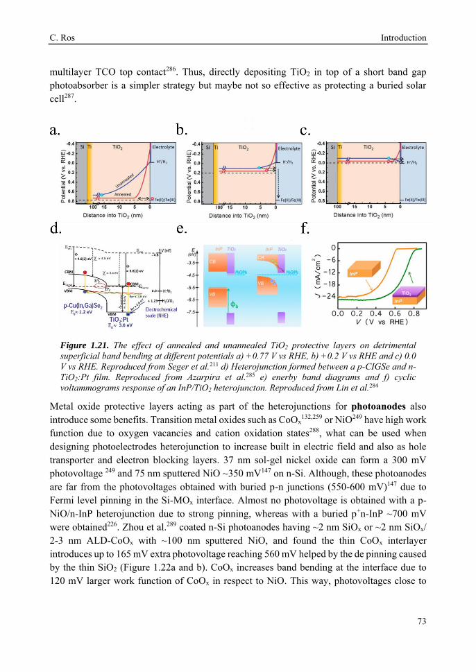
C. Ros Introduction
73
multilayer TCO top contact286. Thus, directly depositing TiO2 in top of a short band gap photoabsorber is a simpler strategy but maybe not so effective as protecting a buried solar cell287.
Figure 1.21. The effect of annealed and unannealed TiO2 protective layers on detrimental superficial band bending at different potentials a) +0.77 V vs RHE, b) +0.2 V vs RHE and c) 0.0 V vs RHE. Reproduced from Seger et al.211 d) Heterojunction formed between a p-CIGSe and n-TiO2:Pt film. Reproduced from Azarpira et al.285 e) enerby band diagrams and f) cyclic voltammograms response of an InP/TiO2 heterojuncton. Reproduced from Lin et al.284
Metal oxide protective layers acting as part of the heterojunctions for photoanodes also introduce some benefits. Transition metal oxides such as CoOx
132,259 or NiO249 have high work function due to oxygen vacancies and cation oxidation states288, what can be used when designing photoelectrodes heterojunction to increase built in electric field and also as hole transporter and electron blocking layers. 37 nm sol-gel nickel oxide can form a 300 mV photovoltage 249 and 75 nm sputtered NiO ~350 mV147 on n-Si. Although, these photoanodes are far from the photovoltages obtained with buried p-n junctions (550-600 mV)147 due to Fermi level pinning in the Si-MOx interface. Almost no photovoltage is obtained with a p-NiO/n-InP heterojunction due to strong pinning, whereas with a buried p+n-InP ~700 mV were obtained226. Zhou et al.289 coated n-Si photoanodes having ~2 nm SiOx or ~2 nm SiOx/ 2-3 nm ALD-CoOx with ~100 nm sputtered NiO, and found the thin CoOx interlayer introduces up to 165 mV extra photovoltage reaching 560 mV helped by the de pinning caused by the thin SiO2 (Figure 1.22a and b). CoOx increases band bending at the interface due to 120 mV larger work function of CoOx in respect to NiO. This way, photovoltages close to
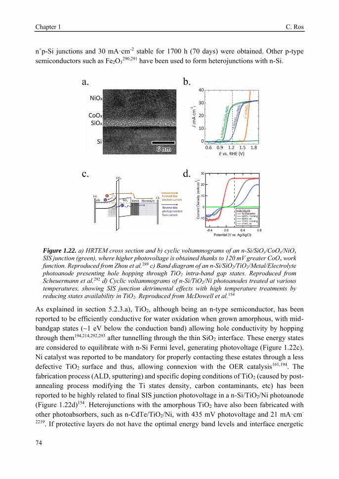
Chapter 1 C. Ros
74
n+p-Si junctions and 30 mA·cm-2 stable for 1700 h (70 days) were obtained. Other p-type semiconductors such as Fe2O3
290,291 have been used to form heterojunctions with n-Si.
Figure 1.22. a) HRTEM cross section and b) cyclic voltammograms of an n-Si/SiOx/CoOx/NiOx SIS junction (green), where higher photovoltage is obtained thanks to 120 mV greater CoOx work function. Reproduced from Zhou et al.289 c) Band diagram of an n-Si/SiO2/TiO2/Metal/Electrolyte photoanode presenting hole hopping through TiO2 intra-band gap states. Reproduced from Scheuermann et al.292 d) Cyclic voltammograms of n-Si/TiO2/Ni photoanodes treated at various temperatures, showing SIS junction detrimental effects with high temperature treatments by reducing states availability in TiO2. Reproduced from McDowell et al.154
As explained in section 5.2.3.a), TiO2, although being an n-type semiconductor, has been reported to be efficiently conductive for water oxidation when grown amorphous, with mid-bandgap states (~1 eV below the conduction band) allowing hole conductivity by hopping through them194,214,292,293 after tunnelling through the thin SiO2 interface. These energy states are considered to equilibrate with n-Si Fermi level, generating photovoltage (Figure 1.22c). Ni catalyst was reported to be mandatory for properly contacting these estates through a less defective TiO2 surface and thus, allowing connexion with the OER catalysis161,194. The fabrication process (ALD, sputtering) and specific doping conditions of TiO2 (caused by post-annealing process modifying the Ti states density, carbon contaminants, etc) has been reported to be highly related to final SIS junction photovoltage in a n-Si/TiO2/Ni photoanode (Figure 1.22d)154. Heterojunctions with the amorphous TiO2 have also been fabricated with other photoabsorbers, such as n-CdTe/TiO2/Ni, with 435 mV photovoltage and 21 mA·cm-
2219. If protective layers do not have the optimal energy band levels and interface energetic

C. Ros Introduction
75
states, degenerately doped layers will screen metallic catalyst work function and limit performance161. Meanwhile, slightly doped protective layers, if thicker, will introduce overpotentials from electrical resistivity, proportional to metal oxide thickness. To prevent this, buried junctions can maximize the obtained photovoltage by themselves, not depending on the protective layer.

Chapter 1 C. Ros
76
7. Buried homojunctions to maximize efficiency and cell flexibility
As it has been analysed in previous section many efforts have been put in forming heterojunctions to directly create a built-in field between the metal oxide protective layer and a short band gap semiconductor. So far, even the achieved photovoltages have been significant, they are not as high as the ones for short band gap semiconductors reported for photovoltaic solar cells (with open circuit potentials of up to 750 mV) 111,294. Buried p-n junctions (Figure 1.12e) have been proven to generate higher built-in electric fields than SCLJ or Schottky junctions, decoupling photoabsorbers Fermi level from that of the metallic or oxide protective layer or electrolyte, also removing a constrain on the catalyst required work function value161,295. This way, a more flexible device design is possible as each component (photoabsorber, protective layer and catalyst) can be selected more independently as it can be observed in Figure 1.23a and b. Thus, several groups have shifted the strategy and worked on adapting solar cell p-n junctions for water splitting, obtaining the highest reported performances of PEC cells132.
Several photovoltaic-used schemes have been studied, being silicon the most implemented one by far. Not only because is the most used one for solar cells, dominating the solar panels market, but also because of the simple and robust cell obtained: a monocrystalline silicon solar cell can be fabricated several tens of centimetres wide, few hundred microns thick and is robust, not requiring any substrate. Also, as p-n junctions are fabricated in silicon wafers by dopant diffusion and incorporation in its crystal lattice at fabrication temperatures of up to 1025 ºC153, further thermal steps applied at medium temperatures (up to 500 ºC) will not damage the p-n junction and will retain original output. In a buried junction electrode, photogenerated charges will migrate to the catalyst/electrolyte interface through protective layers, acting as conductive contacts: n-type semiconductor protective layers should be expected to be prone for electron conductivity in photocathodes (Figure 1.23c), and p-type semiconductors for holes in photoanodes (Figure 1.23d). Although, other strategies such as mid-band gap states in n-type semiconductors have been proposed for hole conduction (Figure 1.23e) or recombining contacts (Figure 1.23f), as will be reviewed later. As example, photovoltages as high as 630 mV have been obtained for silicon with buried p-n junctions294. Other semiconductors have been tested apart from silicon with same protective and catalyst strategies, proving these to be highly reproducible in other photoabsorber materials, increasing device flexibility296.
As it was reported by Scheuermann et al.189 and Wang et. al.296, once a buried junction is introduced in our device, the requirements of the protective layer or the co-catalyst metallic film are reduced. Optimal work function metallic films or cocatalysts to create high electric field with the photoabsorber are no longer needed, widening material selection possibilities. The protective layer just needs to be chemically stable, highly conductive, transparent and the surface must not create electronic barriers with the electrolyte, together with being kinetically
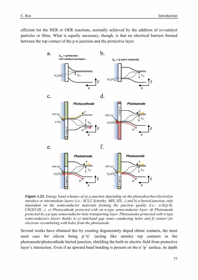
C. Ros Introduction
77
efficient for the HER or OER reactions, normally achieved by the addition of co-catalyst particles or films. What is equally necessary, though, is that no electrical barriers formed between the top contact of the p-n junction and the protective layer.
Figure 1.23. Energy band schemes of a) a junction depending on the photoabsorber/electrolyte interface or intermediate layers (i.e.: SCLJ, Schottky, MIS, SIS…) and b) a buried junction, only dependent on the semiconductor materials forming the junction quality (i.e.: n-Si/p-Si, CIGS/CdS…). c) Photocathode protected with an n-type semiconductor layer. d) Photoanode protected by a p-type semiconductor hole transporting layer. Photoanodes protected with n-type semiconductors layers thanks to e) mid-band gap states conducting holes and f) contact for electrons recombining with holes from the photoanode.
Several works have obtained this by creating degenerately doped ohmic contacts, the most used case for silicon being p+/n+ (acting like metals) top contacts in the photoanode/photocathode buried junction, shielding the built-in electric field from protective layer’s interaction. Even if an upward band bending is present on the n+/p+ surface, its depth

Chapter 1 C. Ros
78
would be limited to few nanometers due to the high doping level, easily permitting charge tunneling through these depletions, facilitating the ohmic contact 180,202,296. Seger et al. introduced a metallic 5 nm Ti film between n+p-Si and MoSx
179 or TiO2122,202, to form an ohmic
contact and to prevent Si oxidation into detrimental insulator SiO2 (Figure 1.24a), meanwhile in a photoanode, for Mei et al.153 a similar structure acted as an ohmic recombining contact between holes from p+-Si and electrons from TiO2 conduction band (Figure 1.24b).
An example of the benefits of a buried junction is the work by Scheuermann et al.189, where they tried to maximize n-Si photoanodes with few nm SiO2 and SiO2/TiO2 layers and Ir catalyst, reaching maximum 500 mV highly sensible to SiO2 thickness, whereas with a buried n+p-Si junction independent 630 mV were obtained. Similar maximum photovoltages for n-Si/p-Si and n+p-Si/p+n-Si PEC electrodes were obtained by other authors117,140,174,179,180,183,189,194,202,210,297.
Figure 1.24. Metallic thin Ti films on degenerately-doped silicon assuring ohmic contacts in a) a photocathode (Reproduced from Bae et al.122) and b) a photoanode, where holes recombine with electrons from the conduction band of the protective layer (Reproduced from Mei et al.232).
Likewise solar cells prospects109, decreasing fabrication costs by depositing thin film photoabsorbers on flexible substrates can help on reducing device costs and facilitating technology implementation298. CIGS-CdS buried junctions have been adapted for water splitting287,299–302, together with their earth-abundant303 equivalent CZTS300,304–306 and In2S3
304,307 or ZnS308,309 to substitute toxic CdS. The capacity of these cells band gap and thus, photovoltage, to be tuned by compositional variations (1.0-1.5 eV)298 reaching record 741 mV photovoltages and 37.8 mA·cm-2 can help to form tandem cells310–313. Metallic Mo/Ti films have been used on CIGS/CdS and increased both photocurrent and onset potential, together with laterally transporting charges and avoiding detrimental interfaces with CdS or Pt particles, and also helped to protect the p-n junction (Figure 1.25a and b)287. Efficiently extracting photogenerated charges in polycrystalline defective materials such as CIGS is important to enhance photovoltage and current, as charge diffusion lengths are significantly lower than in silicon314. In addition, it is known for solar cells that degenerately doped
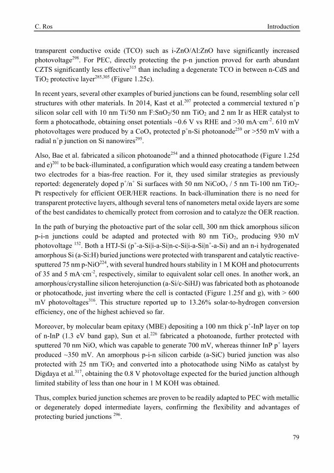
C. Ros Introduction
79
transparent conductive oxide (TCO) such as i-ZnO/Al:ZnO have significantly increased photovoltage298. For PEC, directly protecting the p-n junction proved for earth abundant CZTS significantly less effective315 than including a degenerate TCO in between n-CdS and TiO2 protective layer285,305 (Figure 1.25c).
In recent years, several other examples of buried junctions can be found, resembling solar cell structures with other materials. In 2014, Kast et al.207 protected a commercial textured n+p silicon solar cell with 10 nm Ti/50 nm F:SnO2/50 nm TiO2 and 2 nm Ir as HER catalyst to form a photocathode, obtaining onset potentials ~0.6 V vs RHE and >30 mA·cm-2. 610 mV photovoltages were produced by a CoOx protected p+n-Si photoanode259 or >550 mV with a radial n+p junction on Si nanowires295.
Also, Bae et al. fabricated a silicon photoanode254 and a thinned photocathode (Figure 1.25d and e)201 to be back-illuminated, a configuration which would easy creating a tandem between two electrodes for a bias-free reaction. For it, they used similar strategies as previously reported: degenerately doped p+/n+ Si surfaces with 50 nm NiCoOx / 5 nm Ti-100 nm TiO2-Pt respectively for efficient OER/HER reactions. In back-illumination there is no need for transparent protective layers, although several tens of nanometers metal oxide layers are some of the best candidates to chemically protect from corrosion and to catalyze the OER reaction.
In the path of burying the photoactive part of the solar cell, 300 nm thick amorphous silicon p-i-n junctions could be adapted and protected with 80 nm TiO2, producing 930 mV photovoltage 152. Both a HTJ-Si (p+-a-Si|i-a-Si|n-c-Si|i-a-Si|n+-a-Si) and an n-i hydrogenated amorphous Si (a-Si:H) buried junctions were protected with transparent and catalytic reactive-sputtered 75 nm p-NiO224, with several hundred hours stability in 1 M KOH and photocurrents of 35 and 5 mA·cm-2, respectively, similar to equivalent solar cell ones. In another work, an amorphous/crystalline silicon heterojunction (a-Si/c-SiHJ) was fabricated both as photoanode or photocathode, just inverting where the cell is contacted (Figure 1.25f and g), with > 600 mV photovoltages316. This structure reported up to 13.26% solar-to-hydrogen conversion efficiency, one of the highest achieved so far.
Moreover, by molecular beam epitaxy (MBE) depositing a 100 nm thick p+-InP layer on top of n-InP (1.3 eV band gap), Sun et al.226 fabricated a photoanode, further protected with sputtered 70 nm NiO, which was capable to generate 700 mV, whereas thinner InP p+ layers produced ~350 mV. An amorphous p-i-n silicon carbide (a-SiC) buried junction was also protected with 25 nm TiO2 and converted into a photocathode using NiMo as catalyst by Digdaya et al.317, obtaining the 0.8 V photovoltage expected for the buried junction although limited stability of less than one hour in 1 M KOH was obtained.
Thus, complex buried junction schemes are proven to be readily adapted to PEC with metallic or degenerately doped intermediate layers, confirming the flexibility and advantages of protecting buried junctions 296.

Chapter 1 C. Ros
80
Figure 1.25. a) Charge transfer diagram from the n-type CdS layer to HER catalyst particles (top) and with an intermediate metallic conductive film enabling lateral conduction (bottom) and b) corresponding cyclic voltammograms in 0.5 M Na2SO4, 0.25 M Na2HPO4 and 0.25 M NaH2PO4 (aq.) (pH values adjusted to 6.8 by NaOH addition under AM 1.5G irradiation. Reproduced from Kumagai et al.287 c) Energy band diagram of a CZTS/CdS buried heterojunction protected with AZO/TiO2 layers and Pt catalysed. Reproduced from Rovelli et al.305 d) Back illuminated photoelectrode before thinning and e) after thinning to properly illuminate the p-n junction energy band diagrams. Reproduced from Bae et al.201 Energy band diagrams of p-i-n amorphous silicon f) a photoanode and g) a photocathode showing the role of ohmic contacts, enabling the possibility to easily invert the photoelectrode’s structure by simply inverting the buried junction and selecting different catalysts. Reproduced from Wang et al.316

C. Ros Introduction
81
8. Cell implementation strategies and reactors
In this work, focus has been put on front-illuminated metal oxide or protected photoelectrodes, the strategy followed majorly by authors in the field. Although, solar energy can be used to drive an electrochemical reaction in different implementation strategies, with different grade of external control and device complexity.
8.1. Photoelectrode configuration
Jacobsson et al.23 have methodically described all the possible transitions from an independent monolithic PEC device to an electrolyzer powered by Grid-photovoltaic energy, what is depicted in Figure 1.26.
From a monolithic PEC device (a), the first step is separating with an external circuit the second electrode (b). It is depicted as a metal, but the second one could be photoactive too, combining photovoltage in a tandem design (its characteristics will be discussed later). The second step is introducing a protective layer between the photoabsorber and catalyst, where the junction can be formed between the photoabsorber and the electrolyte/catalyst or the layer can intervene in forming a p-n junction (c). A third step is considered if a vertical catalyst structure is perpendicularly set on the photoabsorber (electrically connected), meanwhile the rest of the surface has the protective layer (d). This way, light can still reach the photoactive semiconductor, meanwhile it is no longer possible to form the depletion with the electrolyte, thus a p-n junction is necessary. Once the vertical catalyst is introduced, next step is directly encapsulating the photoactive part (i.e. into polymer) instead of using a protective layer (e). Once completely isolated, there is no more the need of having the photoactive part inside the electrolyte, and connecting the independent catalyst with a wire to the semiconductor allows freely locating the absorber inside the electrolyte or outside (f). Last step consists of substituting the external photoactive semiconductor with connecting the two remaining catalyst structures with grid photovoltaic (or not) electricity, resulting in a PV-electrolyser setup (g). Jacobsson et al. have implemented several of the mentioned designs in CIGS photoelectrodes301. As the reader may have realized, the technology readiness is not the same for all configurations7: both photovoltaics and electrolysers are already commercialised technologies, compared to PEC ones which are still under significant investigation. But as discussed in section 1, PEC is designed to work at lower current densities, reducing electrochemical overpotentials and enabling higher conversion efficiencies.
Throughout the whole introduction the vast majority of research has been focused in configurations (b) and (c). In-plane electrodes have been reviewed in increasing complexity, a path to increment its built-in electric field, its photon absorption, stability and catalytic efficiency.

Chapter 1 C. Ros
82
Figure 1.26. Scheme of the possible transitions from a monolithic PEC device to a Photovoltaic-grid powered electrolyser. Reproduced from Jacobsson et al.23
8.2. Tandem PEC devices
For non-externally biased (unassisted) single light absorber electrodes, only large band gap semiconductors will create enough photovoltage to break the water molecule, meanwhile a dual absorber tandem structure permits absorbing a larger portion of the solar spectra (Figure 1.27a and b)96,318. As Hu et al.319 calculated, efficiencies higher than 25% should be obtainable (taking into account earth abundant catalysts overpotential and resistance losses) if band gap semiconductors of ~1.1 and 1.6-1.8 eV with high performance are found. The short band gap ones are easy to propose, as candidates are already commercial or under development: Si, GaAs, CIGS or perovskites, but the ones with larger band gap still requires more research. Chalcogenides such as CIGS and CZTS have proven the possibility to tune its band gap from 1.0 to 1.6 eV109,298,309,320,321, and also some perovskites322, what can help in perfect absorption match for both electrodes to be working in the maximum power point.
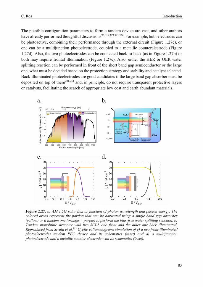
C. Ros Introduction
83
The possible configuration parameters to form a tandem device are vast, and other authors have already performed thoughtful discussions96,318,319,323,324. For example, both electrodes can be photoactive, combining their performance through the external circuit (Figure 1.27c), or one can be a multijunction photoelectrode, coupled to a metallic counterelectrode (Figure 1.27d). Also, the two photoelectrodes can be connected back-to-back (as in Figure 1.27b) or both may require frontal illumination (Figure 1.27c). Also, either the HER or OER water splitting reaction can be performed in front of the short band gap semiconductor or the large one, what must be decided based on the protection strategy and stability and catalyst selected. Back-illuminated photoelectrodes are good candidates if the large band gap absorber must be deposited on top of them201,254 and, in principle, do not require transparent protective layers or catalysts, facilitating the search of appropriate low cost and earth abundant materials.
Figure 1.27. a) AM 1.5G solar flux as function of photon wavelength and photon energy. The colored areas represent the portion that can be harvested using a single band gap absorber (yellow) or a tandem one (orange + purple) to perform the bias-free water splitting reaction. b) Tandem monolithic structure with two SCLJ, one front and the other one back illuminated. Reproduced from Sivula et al.318 Cyclic voltammograms simulation of c) a two front-illuminated photoelectrodes tandem PEC device and its schematics (inset) and d) a multijunction photoelectrode and a metallic counter electrode with its schematics (inset).
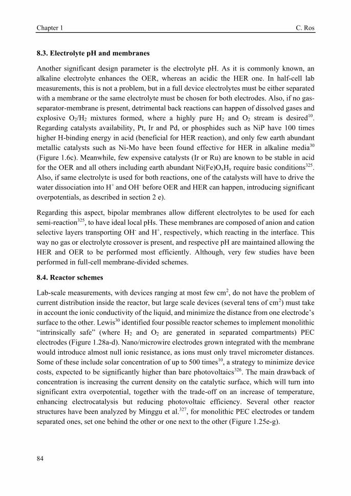
Chapter 1 C. Ros
84
8.3. Electrolyte pH and membranes
Another significant design parameter is the electrolyte pH. As it is commonly known, an alkaline electrolyte enhances the OER, whereas an acidic the HER one. In half-cell lab measurements, this is not a problem, but in a full device electrolytes must be either separated with a membrane or the same electrolyte must be chosen for both electrodes. Also, if no gas-separator-membrane is present, detrimental back reactions can happen of dissolved gases and explosive O2/H2 mixtures formed, where a highly pure H2 and O2 stream is desired10. Regarding catalysts availability, Pt, Ir and Pd, or phosphides such as NiP have 100 times higher H-binding energy in acid (beneficial for HER reaction), and only few earth abundant metallic catalysts such as Ni-Mo have been found effective for HER in alkaline media30 (Figure 1.6c). Meanwhile, few expensive catalysts (Ir or Ru) are known to be stable in acid for the OER and all others including earth abundant Ni(Fe)OxHy require basic conditions325. Also, if same electrolyte is used for both reactions, one of the catalysts will have to drive the water dissociation into H+ and OH- before OER and HER can happen, introducing significant overpotentials, as described in section 2 e).
Regarding this aspect, bipolar membranes allow different electrolytes to be used for each semi-reaction325, to have ideal local pHs. These membranes are composed of anion and cation selective layers transporting OH- and H+, respectively, which reacting in the interface. This way no gas or electrolyte crossover is present, and respective pH are maintained allowing the HER and OER to be performed most efficiently. Although, very few studies have been performed in full-cell membrane-divided schemes.
8.4. Reactor schemes
Lab-scale measurements, with devices ranging at most few cm2, do not have the problem of current distribution inside the reactor, but large scale devices (several tens of cm2) must take in account the ionic conductivity of the liquid, and minimize the distance from one electrode’s surface to the other. Lewis30 identified four possible reactor schemes to implement monolithic “intrinsically safe” (where H2 and O2 are generated in separated compartments) PEC electrodes (Figure 1.28a-d). Nano/microwire electrodes grown integrated with the membrane would introduce almost null ionic resistance, as ions must only travel micrometer distances. Some of these include solar concentration of up to 500 times10, a strategy to minimize device costs, expected to be significantly higher than bare photovoltaics326. The main drawback of concentration is increasing the current density on the catalytic surface, which will turn into significant extra overpotential, together with the trade-off on an increase of temperature, enhancing electrocatalysis but reducing photovoltaic efficiency. Several other reactor structures have been analyzed by Minggu et al.327, for monolithic PEC electrodes or tandem separated ones, set one behind the other or one next to the other (Figure 1.25e-g).
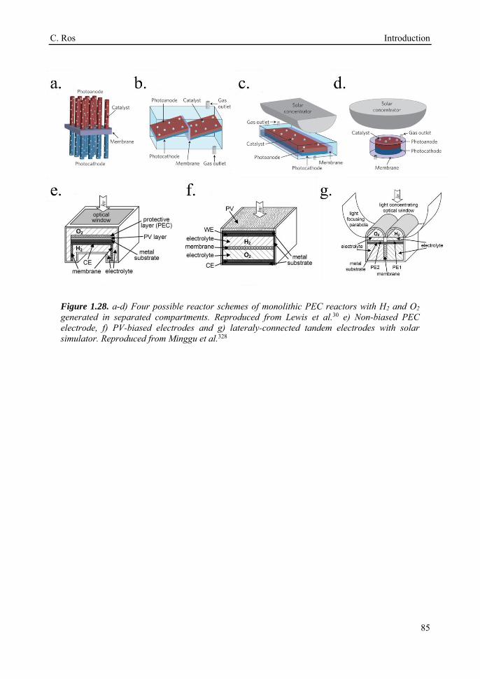
C. Ros Introduction
85
Figure 1.28. a-d) Four possible reactor schemes of monolithic PEC reactors with H2 and O2 generated in separated compartments. Reproduced from Lewis et al.30 e) Non-biased PEC electrode, f) PV-biased electrodes and g) lateraly-connected tandem electrodes with solar simulator. Reproduced from Minggu et al.328
Chapter 1 C. Ros
86
9. Resume, perspective and challenges
Renewable energy sources will eventually be implemented globally, together with energy carriers capable to be distributed and used when necessary. PEC water splitting has demonstrated to produce hydrogen from solar energy and water with significant efficiencies, although this technology is not ready for market implementation due to lack of efficient, stable and scalable photoelectrodes.
In this introduction, the pathway of last decades investigations on PEC water splitting cells has been analysed. After first discovery of the semiconductor-liquid junction producing few µA·cm-2 photocurrents on TiO2, several other semiconductor materials have been tested and modified in the search of an efficient, stable and scalable device, with significant advances obtained. Other metal oxides such as Fe2O3, WO3, BiVO4, or Cu2O have been nanostructured and treated to maximize the built-in electric field to enhance electron-hole separation and transport, together with co-catalyst decoration for a more efficient HER/OER reaction. Metal oxide photoelectrodes present good stability in oxidizing environments and are scalable due to earth abundant materials and low cost deposition techniques, but up to now have lacked of significant photocurrent efficiency.
An alternative approach to overcome this has been adapting short band gap materials such as the ones used for the photovoltaic industry into PEC, mostly III-V semiconductors like GaAs, CdTe or InP, or earth abundant Si, CIGS and CZTS. 1.0 to 1.8 eV band gap semiconductors are capable to absorb broad part of the solar spectra, and some of these materials are band gap tunable by composition variations like In/Ga for CIGS and S/Se in CZTS, easing implementation in tandem devices. Although, their main drawback is the instability in aqueous acidic or alkaline electrolytes.
During las decade, metallic films have been deposited on top both as catalysts and to prevent corrosion, but few nanometer thick layers, thin enough to be transparent, were not passivating enough. Tunnel-distances-thick oxides present similar problems, as resistance increases dramatically if more than ~5 nm are deposited. But protecting short band gap photoabsorbers, containing a buried junction, with semiconductor metal oxide transparent conducting and protective layers several tens of nanometers thick has enabled more than 1000 h stable electrodes, with photocurrents and photovoltages resembling photovoltaic cells. TiO2 and NiO have been the most studied and best performing protective layers, the former with Pt or Ni as HER/OER catalysts and the latter being OER catalytic too.
Yet, electron or hole conduction mechanisms across protective layers are still not fully understood, in photoabsorber-film interface, across the layer or in the layer-catalyst-electrolyte electrolytic surface. Especially for TiO2 but also for NiO protective layers, the nanoscale disorder and thus, deposition process and temperature have presented significant variations among different studies. Moreover, intrinsic stability for these materials for very
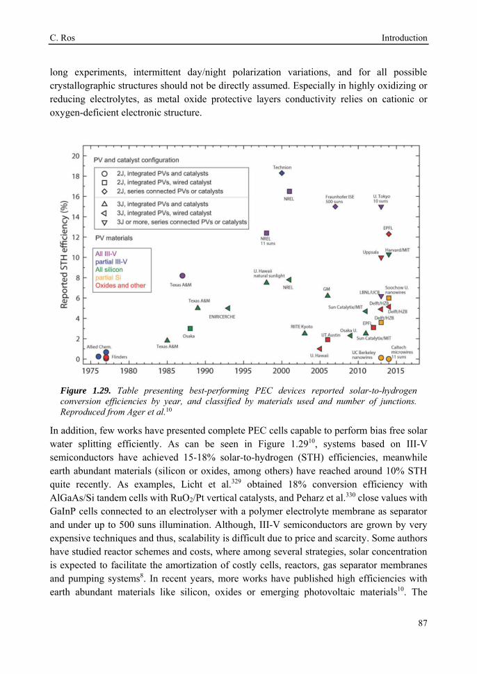
C. Ros Introduction
87
long experiments, intermittent day/night polarization variations, and for all possible crystallographic structures should not be directly assumed. Especially in highly oxidizing or reducing electrolytes, as metal oxide protective layers conductivity relies on cationic or oxygen-deficient electronic structure.
Figure 1.29. Table presenting best-performing PEC devices reported solar-to-hydrogen conversion efficiencies by year, and classified by materials used and number of junctions. Reproduced from Ager et al.10
In addition, few works have presented complete PEC cells capable to perform bias free solar water splitting efficiently. As can be seen in Figure 1.2910, systems based on III-V semiconductors have achieved 15-18% solar-to-hydrogen (STH) efficiencies, meanwhile earth abundant materials (silicon or oxides, among others) have reached around 10% STH quite recently. As examples, Licht et al.329 obtained 18% conversion efficiency with AlGaAs/Si tandem cells with RuO2/Pt vertical catalysts, and Peharz et al.330 close values with GaInP cells connected to an electrolyser with a polymer electrolyte membrane as separator and under up to 500 suns illumination. Although, III-V semiconductors are grown by very expensive techniques and thus, scalability is difficult due to price and scarcity. Some authors have studied reactor schemes and costs, where among several strategies, solar concentration is expected to facilitate the amortization of costly cells, reactors, gas separator membranes and pumping systems8. In recent years, more works have published high efficiencies with earth abundant materials like silicon, oxides or emerging photovoltaic materials10. The

Chapter 1 C. Ros
88
Department of Energy (D.O.E.) of the United States fixed a road map for PEC water splitting pointing at 15% STH and $17.30 per kg H2 by 2015, 20% STH and $5.70 per kg H2 by 2020, and ultimately 25% STH and $2.10 per kg H2
10. Efficiencies close to the 2015 and 2020 goals have been obtained nowadays, but on lab-scale devices and with high cost materials.
In order to implement PEC water splitting at industrial scale, efforts must be put into the fabrication of efficient, stable and scalable photoelectrodes. Stable semiconductor materials fulfilling these requirements must be researched and, although some examples like WSe have shown promising results331, the best strategy nowadays is protecting photoabsorbers as such used in PV for long term operation. TiO2, NiO or CoOx have been the best performing protective layers so far, fabricated by reactive sputtering, CVD or ALD to minimize pinhole formation. The substitution of high vacuum deposition and time consuming techniques would reduce fabrication costs if non-pinhole layers can be assured, meanwhile self-limited corrosion candidates such as native SiO2 in silicon protected electrodes in acidic environments must be found (where it is passivated only where pinholes are present in the protective layer)132. Using the protective layer as antireflective layer will for sure help in increasing photoelectrodes productivity147.
More full cell reactor field tests should be performed for sure next decade to fully understand complete device stability and degradation mechanisms332, especially in less-controlled environments, under day/night intermittent operation, temperature changes and mechanical impact caused by bubbling or electrolyte pumping6,333,334. Regenerative strategies like electrocatalyst re-deposition in dark conditions at night could reduce a constrain, increasing available material candidates272,335,336.
Although some authors have claimed demonstration or early-stage commercial devices would be possible with noble metals if cost-efficiency is matched, earth abundant alternatives must be researched for large scale deployment6. Bias-free tandem cells will require medium band-gap semiconductors to be coupled with short ones, and chalcogenides or perovskites (band gap tunable by composition control) have shown promising results for solar cells109. In addition, finding earth abundant transparent and conductive catalysts, especially inexistent for OER in acid and HER in alkaline, would reduce the constrains on selecting electrolytes and reactions performed on each side. Protective layers with superficial energetics prone to enhance HER or OER catalysis would simplify even more the structures. NiO protective layers surface incorporates Fe and forms Ni(Fe)OOH in alkaline media, one of the most efficient earth abundant OER catalysts147, or MoS2 protective and transparent layers have been recently grown and reported stable in acid with good HER catalysis273.
Furthermore, during last decade some authors have used photoelectrochemistry for other reactions besides water splitting. Carbon dioxide reduction reaction (CO2RR) is far more complex than water splitting, but enables the possibility to extract the greenhouse gas CO2 from the atmosphere and turn it into a reusable fuel or chemical. Commercial products like

C. Ros Introduction
89
methane or ethanol production from CO2 reduction have been studied, which could directly be incorporated into the actual carbon-based fossil fuels marked, and several other molecules are possible with appropriate catalysts. The possibility of obtaining liquid products is especially interesting, as highly simplifies distribution and storage (some of the main drawbacks for H2 as energy vector implementation). Main challenges for CO2 reduction are finding appropriate catalysts and stable semiconductors to be placed in direct contact with the reaction, as the higher required reductive potentials (~1 extra volt) enhance materials corrosion337,338.

Chapter 1 C. Ros
90
C. Ros Introduction
91
10. Scope of this research
The main objective of this thesis is to study efficient and stable photoelectrodes for PEC water splitting as renewable energy conversion and storage technology for Solar Fuels, using cost-effective materials and scalable techniques. The thesis is mainly focused on improving the efficiency of metal oxide photoelectrodes and on stabilizing efficient photoabsorber semiconductors with protective layers. This includes studying earth abundant efficient materials already known from photovoltaics and optimizing its adaptation into PEC water splitting, mainly charge separation and transport to the electrochemical reaction while avoiding degradation. Some of the specific objectives of this thesis have been:
• Finding appropriate band gap materials to work as photoanodes or photocathodes, with special interest in earth abundant materials, capable of high productivities and long lasting stabilities in harsh acidic and basic electrolytes.
• Maximizing the productivity of metal oxide-based photoelectrodes by nanostructuration and modifying the electronic structure.
• Adapting semiconductors already known from photovoltaic technology as both photocathodes and photoanodes. This includes monocrystalline or other configuration silicon cells and alternative semiconductors.
• Inhibiting corrosion of unstable photoabsorber candidates in highly acidic or basic electrolytes by deposition of protective layers, with special concern on avoiding detrimental affectations on the photoabsorber efficiency.
• Studying atomic layer deposition as protection technique. Controlling the effect of deposition parameters to obtain transparent, conductive and stable protective films.
• Identifying key parameters for efficient conductivity through protective layers both macroscopically and at the nanoscale. Characterizing protective layers before and after long-term operation, with special concern on intrinsic instabilities in harsh electrolytes. This includes identifying the role of introduced overlayers and interfaces.
• Characterizing protected semiconductors as PEC water splitting photo electrodes, identifying the elements limiting productivity related to electrical transport and electrochemical activity.
• Studying the main degradation mechanisms to efficient and long stable photoelectrodes and identifying possible ways to revert them.
Chapter 1 C. Ros
92
Bibliography
(1) Heinberg, R.; Fridley, D. Our Renewable Future; Island Press, 2016.
(2) Godoy, J. M. 210 Pb Sediment Dating: Redeeming the History of Environmental Pollution in the Anthropocene. Rev. Virtual Quim. 2018, 10 (6), 1733–1757.
(3) Berry, G. D.; Pasternak, A. D.; Rambach, G. D.; Smith, J. R.; Schock, R. N. Hydrogen as a Future Transportation Fuel. Energy 1996, 21 (4), 289–303.
(4) Fujishima, A.; Honda, K. Electrochemical Photolysis of Water at a Semiconductor Electrode. Nature 1972, 238 (5358), 37–38.
(5) Li, Z.; Feng, J.; Yan, S.; Zou, Z. Solar Fuel Production: Strategies and New Opportunities with Nanostructures. Nano Today 2015, 1–19.
(6) McKone, J. R.; Lewis, N. S.; Gray, H. B. Will Solar-Driven Water-Splitting Devices See the Light of Day? Chem. Mater. 2014, 26 (1), 407–414.
(7) Ardo, S.; Fernandez Rivas, D.; Modestino, M. A.; Schulze Greiving, V.; Abdi, F. F.; Alarcon-Llado, E.; Artero, V.; Ayers, K. E.; Battaglia, C.; Becker, J.-P.; et al. Pathways to Electrochemical Solar-Hydrogen Technologies. Energy Environ. Sci. 2018, 0–45.
(8) Shaner, M. R.; Atwater, H. A.; Lewis, N. S.; McFarland, E. W. A Comparative Technoeconomic Analysis of Renewable Hydrogen Production Using Solar Energy. Energy Environ. Sci. 2016, 9 (7), 2354–2371.
(9) Rothschild, A.; Dotan, H. Beating the Efficiency of Photovoltaics-Powered Electrolysis with Tandem Cell Photoelectrolysis. ACS Energy Lett. 2017, 2 (1), 45–51.
(10) Ager, J. W.; Shaner, M. R.; Walczak, K. A.; Sharp, I. D.; Ardo, S. Experimental Demonstrations of Spontaneous, Solar-Driven Photoelectrochemical Water Splitting. Energy Environ. Sci. 2015, 8, 2811–2824.
(11) Görlin, M.; Chernev, P.; De Araújo, J. F.; Reier, T.; Dresp, S.; Paul, B.; Krähnert, R.; Dau, H.; Strasser, P. Oxygen Evolution Reaction Dynamics, Faradaic Charge Efficiency, and the Active Metal Redox States of Ni-Fe Oxide Water Splitting Electrocatalysts. J. Am. Chem. Soc. 2016, 138 (17), 5603–5614.
(12) Dutta, A.; Pradhan, N. Developments of Metal Phosphides as Efficient OER Precatalysts. J. Phys. Chem. Lett. 2016, 144–152.
(13) Benck, J. D.; Hellstern, T. R.; Kibsgaard, J.; Chakthranont, P.; Jaramillo, T. F. Catalyzing the Hydrogen Evolution Reaction (HER) with Molybdenum Sulfide Nanomaterials. ACS Catal. 2014, 4 (11), 3957–3971.
(14) Yan, Y.; Xia, B.; Xu, Z.; Wang, X. Recent Development of Molybdenum Sulfides as Advanced Electrocatalysts for Hydrogen Evolution Reaction. ACS Catal. 2014, 4 (6), 1693–1705.
(15) Gong, M.; Dai, H. A Mini Review of NiFe-Based Materials as Highly Active Oxygen Evolution Reaction Electrocatalysts. Nano Res. 2014, 8 (1), 23–39.
(16) Trotochaud, L.; Ranney, J. K.; Williams, K. N.; Boettcher, S. W. Solution-Cast Metal Oxide Thin Film Electrocatalysts for Oxygen Evolution. J. Am. Chem. Soc. 2012, 134 (41), 17253–17261.
C. Ros Introduction
93
(17) Sheng, W.; Gasteiger, H. A.; Shao-Horn, Y. Hydrogen Oxidation and Evolution Reaction Kinetics on Platinum: Acid vs Alkaline Electrolytes. J. Electrochem. Soc. 2010, 157 (11), B1529.
(18) Trasatti, S. The Absolute Electrode Potential : An Explanatory Note. Pure AppL Chem., 1986, 58 (7), 955–966.
(19) Li, H.; Chen, S.; Zhang, Y.; Zhang, Q.; Zhang, Q.; Jia, X.; Gu, L.; Sun, X.; Song, L.; Wang, X. Systematic Design of Superaerophobic Nanotube-Array Electrode Comprised of Transition-Metal Sulfides for Overall Water Splitting. Nat. Commun. 2018, 9 (1), 1–12.
(20) Yu, Z. Y.; Lang, C. C.; Gao, M. R.; Chen, Y.; Fu, Q. Q.; Duan, Y.; Yu, S. H. Ni-Mo-O Nanorod-Derived Composite Catalysts for Efficient Alkaline Water-to-Hydrogen Conversion: Via Urea Electrolysis. Energy Environ. Sci. 2018, 11 (7), 1890–1897.
(21) Helmholtz, H. Studien Über Electrische Grenzschichten. Ann. der Phys. und Chemie 1879, 243 (7), 337–382.
(22) Newman, O.; Thomas-Alyea, K. E. Electrochemical Systems; John Wiley & Sons, H., Ed.; 2004.
(23) Jacobsson, T. J.; Fjällström, V.; Edoff, M.; Edvinsson, T. Sustainable Solar Hydrogen Production: From Photoelectrochemical Cells to PV-Electrolyzers and Back Again. Energy Environ. Sci. 2014, 7 (7), 2056.
(24) Murphy, A. B.; Barnes, P. R. F.; Randeniya, L. K.; Plumb, I. C.; Grey, I. E.; Horne, M. D.; Glasscock, J. A. Efficiency of Solar Water Splitting Using Semiconductor Electrodes. Int. J. Hydrogen Energy 2006, 31 (14), 1999–2017.
(25) Chen, Z.; Dinh, H. N.; Miller, E. Photoelectrochemical Water Splitting - Standards, Experimental Methods, and Protocols; Springer, 2013.
(26) Jiang, C.; Moniz, S. J. A.; Wang, A.; Zhang, T.; Tang, J. Photoelectrochemical Devices for Solar Water Splitting - Materials and Challenges. Chem. Soc. Rev. 2017, 46 (15), 4645–4660.
(27) Li, J.; Wu, N. Semiconductor-Based Photocatalysts and Photoelectrochemical Cells for Solar Fuel Generation: A Review. Catal. Sci. Technol. 2015, No. 3, 1360.
(28) Smith, W. A.; Sharp, I. D.; Strandwitz, N. C.; Bisquert, J. Interfacial Band-Edge Energetics for Solar Fuels Production. Energy Environ. Sci. 2015, 8 (10), 2851–2862.
(29) Yang, Y.; Niu, S.; Han, D.; Liu, T.; Wang, G.; Li, Y. Progress in Developing Metal Oxide Nanomaterials for Photoelectrochemical Water Splitting. Adv. Energy Mater. 2017, 7 (19), 1–26.
(30) Lewis, N. S. Developing a Scalable Artificial Photosynthesis Technology through Nanomaterials by Design. Nat. Nanotechnol. 2016, 11 (12), 1010–1019.
(31) Chen, S.; Wang, L. W. Thermodynamic Oxidation and Reduction Potentials of Photocatalytic Semiconductors in Aqueous Solution. Chem. Mater. 2012, 24 (18), 3659–3666.
(32) Berger, T.; Monllor-Satoca, D.; Jankulovska, M.; Lana-Villarreal, T.; Gómez, R. The Electrochemistry of Nanostructured Titanium Dioxide Electrodes. ChemPhysChem 2012, 13 (12), 2824–2875.
Chapter 1 C. Ros
94
(33) Wang, J.; Liu, X.; Li, R.; Qiao, P.; Xiao, L.; Fan, J. TiO 2 Nanoparticles with Increased Surface Hydroxyl Groups and Their Improved Photocatalytic Activity. Catal. Commun. 2012, 19, 96–99.
(34) Jankulovska, M.; Berger, T.; Wong, S. S.; Gómez, R.; Lana-Villarreal, T. Trap States in TiO2 Films Made of Nanowires, Nanotubes or Nanoparticles: An Electrochemical Study. ChemPhysChem 2012, 13 (12), 3008–3017.
(35) Fan, J.; Fàbrega, C.; Zamani, R. R.; Hao, Y.; Parra, A.; Andreu, T.; Arbiol, J.; Boschloo, G.; Hagfeldt, A.; Morante, J. R.; et al. Enhanced Photovoltaic Performance of Nanowire Dye-Sensitized Solar Cells Based on Coaxial TiO2@TiO Heterostructures with a Cobalt(II/III) Redox Electrolyte. ACS Appl. Mater. Interfaces 2013, 5 (20), 9872–9877.
(36) Sá, J.; Friedli, P.; Geiger, R.; Lerch, P.; Rittmann-Frank, M. H.; Milne, C. J.; Szlachetko, J.; Santomauro, F. G.; van Bokhoven, J. a; Chergui, M.; et al. Transient Mid-IR Study of Electron Dynamics in TiO2 Conduction Band. Analyst 2013, 138 (7), 1966.
(37) Kim, J. Y.; Magesh, G.; Youn, D. H.; Jang, J. W.; Kubota, J.; Domen, K.; Lee, J. S. Single-Crystalline, Wormlike Hematite Photoanodes for Efficient Solar Water Splitting. Sci. Rep. 2013, 3, 1–8.
(38) Dias, P.; Vilanova, A.; Lopes, T.; Andrade, L.; Mendes, A. Extremely Stable Bare Hematite Photoanode for Solar Water Splitting. Nano Energy 2016, 23, 70–79.
(39) Sivula, K.; Le Formal, F.; Grätzel, M. Solar Water Splitting: Progress Using Hematite (α-Fe 2O3) Photoelectrodes. ChemSusChem 2011, 4 (4), 432–449.
(40) Wei, Y.; Ke, L.; Kong, J.; Liu, H.; Jiao, Z.; Lu, X.; Du, H.; Sun, X. W. Enhanced Photoelectrochemical Water-Splitting Effect with a Bent ZnO Nanorod Photoanode Decorated with Ag Nanoparticles. Nanotechnology 2012, 23 (23).
(41) Wang, B. S.; Li, R. Y.; Zhang, Z. Y.; Xing-Wang; Wu, X. L.; Cheng, G. A.; Zheng, R. T. An Overlapping ZnO Nanowire Photoanode for Photoelectrochemical Water Splitting. Catal. Today 2019, 321–322 (July 2017), 100–106.
(42) Zheng, J. Y.; Song, G.; Hong, J.; Van, T. K.; Pawar, A. U.; Kim, D. Y.; Kim, C. W.; Haider, Z.; Kang, Y. S. Facile Fabrication of WO3nanoplates Thin Films with Dominant Crystal Facet of (002) for Water Splitting. Cryst. Growth Des. 2014, 14 (11), 6057–6066.
(43) Su, J.; Feng, X.; Sloppy, J. D.; Guo, L.; Grimes, C. A. Vertically Aligned WO3 Nanowire Arrays Grown Directly on Transparent Conducting Oxide Coated Glass: Synthesis and Photoelectrochemical Properties. Nano Lett. 2011, 11 (1), 203–208.
(44) Fàbrega, C.; Murcia-López, S.; Monllor-Satoca, D.; Prades, J. D.; Hernández-Alonso, M. D.; Penelas, G.; Morante, J. R.; Andreu, T. Efficient WO3 Photoanodes Fabricated by Pulsed Laser Deposition for Photoelectrochemical Water Splitting with High Faradaic Efficiency. Appl. Catal. B Environ. 2016, 189, 133–140.
(45) Kim, T. W.; Choi, K.-S. Improving Stability and Photoelectrochemical Performance of BiVO 4 Photoanodes in Basic Media by Adding a ZnFe 2 O 4 Layer. J. Phys. Chem. Lett. 2016, 7 (3), 447–451.
(46) Seabold, J. A.; Choi, K. S. Efficient and Stable Photo-Oxidation of Water by a Bismuth Vanadate Photoanode Coupled with an Iron Oxyhydroxide Oxygen Evolution Catalyst. J. Am.

C. Ros Introduction
95
Chem. Soc. 2012, 134 (4), 2186–2192.
(47) Abdi, F. F.; Van De Krol, R. Nature and Light Dependence of Bulk Recombination in Co-Pi-Catalyzed BiVO4 Photoanodes. J. Phys. Chem. C 2012, 116 (17), 9398–9404.
(48) Berglund, S. P.; Flaherty, D. W.; Hahn, N. T.; Bard, A. J.; Mullins, C. B. Photoelectrochemical Oxidation of Water Using Nanostructured BiVO 4 Films. J. Phys. Chem. C 2011, 115 (9), 3794–3802.
(49) Hu, C.; Chu, K.; Zhao, Y.; Teoh, W. Y. Efficient Photoelectrochemical Water Splitting over Anodized P-Type NiO Porous Films. ACS Appl. Mater. Interfaces 2014, 6 (21), 18558–18568.
(50) Wick, R.; Tilley, S. D. Photovoltaic and Photoelectrochemical Solar Energy Conversion with Cu2O. J. Phys. Chem. C 2015, 119 (47), 26243–26257.
(51) Bard, A. J. Thermodynamic Potential for the Anodic Dissolution of N-Type Semiconductors. J. EIectrochem. Soc. Electrochem. Sci. Technol. 1977, 1706–1710.
(52) Gerischer, H. On the Stability of Semiconductor Electrodes against Photodecomposition. J. Electroanal. Chem. 1977, 82, 133–143.
(53) Luo, J.; Steier, L.; Son, M. K.; Schreier, M.; Mayer, M. T.; Grätzel, M. Cu2O Nanowire Photocathodes for Efficient and Durable Solar Water Splitting. Nano Lett. 2016, 16 (3), 1848–1857.
(54) Li, J.; Wu, N. Semiconductor-Based Photocatalysts and Photoelectrochemical Cells for Solar Fuel Generation: 2015, 5 (3).
(55) Toma, F. M.; Cooper, J. K.; Kunzelmann, V.; McDowell, M. T.; Yu, J.; Larson, D. M.; Borys, N. J.; Abelyan, C.; Beeman, J. W.; Yu, K. M.; et al. Mechanistic Insights into Chemical and Photochemical Transformations of Bismuth Vanadate Photoanodes. Nat. Commun. 2016, 7 (May), 1–11.
(56) Jang, Y. J.; Park, Y. Bin; Kim, H. E.; Choi, Y. H.; Choi, S. H.; Lee, J. S. Oxygen-Intercalated CuFeO2 Photocathode Fabricated by Hybrid Microwave Annealing for Efficient Solar Hydrogen Production. Chem. Mater. 2016, 28 (17), 6054–6061.
(57) Yin, W. J.; Tang, H.; Wei, S. H.; Al-Jassim, M. M.; Turner, J.; Yan, Y. Band Structure Engineering of Semiconductors for Enhanced Photoelectrochemical Water Splitting: The Case of TiO2. Phys. Rev. B - Condens. Matter Mater. Phys. 2010, 82 (4), 1–6.
(58) Wang, G.; Xiao, X.; Li, W.; Lin, Z.; Zhao, Z.; Chen, C.; Wang, C.; Li, Y.; Huang, X.; Miao, L.; et al. Significantly Enhanced Visible Light Photoelectrochemical Activity in TiO2 Nanowire Arrays by Nitrogen Implantation. Nano Lett. 2015, 15 (7), 4692–4698.
(59) Wang, G.; Wang, H.; Ling, Y.; Tang, Y.; Yang, X.; Fitzmorris, R. C.; Wang, C.; Zhang, J. Z.; Li, Y. Hydrogen-Treated TiO2 Nanowire Arrays for Photoelectrochemical Water Splitting. Nano Lett. 2011, 11 (7), 3026–3033.
(60) Yang, C.; Wang, Z.; Lin, T.; Yin, H.; Lü, X.; Wan, D.; Xu, T.; Zheng, C.; Lin, J.; Huang, F.; et al. Core-Shell Nanostructured “Black” Rutile Titania as Excellent Catalyst for Hydrogen Production Enhanced by Sulfur Doping. J. Am. Chem. Soc. 2013, 135 (47), 17831–17838.
(61) Fàbrega, C.; Andreu, T.; Güell, F.; Prades, J. D.; Estradé, S.; Rebled, J. M.; Peiró, F.; Morante, J. R. Effectiveness of Nitrogen Incorporation to Enhance the Photoelectrochemical Activity of
Chapter 1 C. Ros
96
Nanostructured TiO2:NH3 versus H2-N2 Annealing. Nanotechnology 2011, 22 (23), 235403.
(62) Wang, F.; Di Valentin, C.; Pacchioni, G. Doping of WO3for Photocatalytic Water Splitting: Hints from Density Functional Theory. J. Phys. Chem. C 2012, 116 (16), 8901–8909.
(63) Wang, F.; DiValentin, C.; Pacchioni, G. Rational Band Gap Engineering of WO 3 Photocatalyst for Visible Light Water Splitting. ChemCatChem 2012, 4 (4), 476–478.
(64) Hart, J. N.; Cutini, M.; Allan, N. L. Band Gap Modification of ZnO and ZnS through Solid Solution Formation for Applications in Photocatalysis. Energy Procedia 2014, 60 (C), 32–36.
(65) Hamid, S. B. A.; Teh, S. J.; Lai, C. W. Photocatalytic Water Oxidation on ZnO: A Review. Catalysts 2017, 7 (3), 93.
(66) Wang, M.; Ren, F.; Zhou, J.; Cai, G.; Cai, L.; Hu, Y.; Wang, D.; Liu, Y.; Guo, L.; Shen, S. N Doping to ZnO Nanorods for Photoelectrochemical Water Splitting under Visible Light: Engineered Impurity Distribution and Terraced Band Structure. Sci. Rep. 2015, 5 (1), 12925.
(67) Wang, T.; Luo, Z.; Li, C.; Gong, J. Controllable Fabrication of Nanostructured Materials for Photoelectrochemical Water Splitting via Atomic Layer Deposition. Chem. Soc. Rev. 2014, 43 (22), 7469–7484.
(68) Kang, Q.; Cao, J.; Zhang, Y.; Liu, L.; Xu, H.; Ye, J. Reduced TiO2 Nanotube Arrays for Photoelectrochemical Water Splitting. J. Mater. Chem. A 2013, 1 (18), 5766.
(69) Fàbrega, C.; Hernández-Ramírez, F.; Daniel Prades, J.; Jiménez-Díaz, R.; Andreu, T.; Ramon Morante, J. On the Photoconduction Properties of Low Resistivity TiO2 Nanotubes. Nanotechnology 2010, 21 (44).
(70) Yang, Y.; Kao, L. C.; Liu, Y.; Sun, K.; Yu, H.; Guo, J.; Liou, S. Y. H.; Hoffmann, M. R. Cobalt-Doped Black TiO2Nanotube Array as a Stable Anode for Oxygen Evolution and Electrochemical Wastewater Treatment. ACS Catal. 2018, 8 (5), 4278–4287.
(71) Fàbrega, C.; Andreu, T.; Tarancón, A.; Flox, C.; Morata, A.; Calvo-Barrio, L.; Morante, J. R. Optimization of Surface Charge Transfer Processes on Rutile TiO2 Nanorods Photoanodes for Water Splitting. Int. J. Hydrogen Energy 2013, 38 (7), 2979–2985.
(72) Wu, J. M.; Zhang, T. W.; Zeng, Y. W.; Hayakawa, S.; Tsuru, K.; Osaka, A. Large-Scale Preparation of Ordered Titania Nanorods with Enhanced Photocatalytic Activity. Langmuir 2005, 21 (15), 6995–7002.
(73) Fàbrega, C.; Monllor-Satoca, D.; Ampudia, S.; Parra, A.; Andreu, T.; Morante, J. R. Tuning the Fermi Level and the Kinetics of Surface States of TiO2 Nanorods by Means of Ammonia Treatments. J. Phys. Chem. C 2013, 117 (40), 20517–20524.
(74) Rao, P. M.; Cai, L.; Liu, C.; Cho, I. S.; Lee, C. H.; Weisse, J. M.; Yang, P.; Zheng, X. Simultaneously Efficient Light Absorption and Charge Separation in WO3/BiVO4 Core/Shell Nanowire Photoanode for Photoelectrochemical Water Oxidation. Nano Lett. 2014, 14 (2), 1099–1105.
(75) Yang, X.; Liu, R.; Lei, Y.; Li, P.; Wang, K.; Zheng, Z.; Wang, D. Dual Influence of Reduction Annealing on Diffused Hematite/FTO Junction for Enhanced Photoelectrochemical Water Oxidation. ACS Appl. Mater. Interfaces 2016, 8 (25), 16476–16485.
(76) Mor, G. K.; Varghese, O. K.; Wilke, R. H. T.; Sharma, S.; Shankar, K.; Latempa, T. J.; Choi,
C. Ros Introduction
97
K.; Grimes, C. A. P-Type Cu Ti O Nanotube Arrays and Their Use in Self-Biased Heterojunction Photoelectrochemical Diodes for Hydrogen Generation. 2008, 0–5.
(77) Paracchino, A.; Laporte, V.; Sivula, K.; Grätzel, M.; Thimsen, E. Highly Active Oxide Photocathode for Photoelectrochemical Water Reduction. Nat. Mater. 2011, 10 (6), 456–461.
(78) Zhou, M.; Bao, J.; Xu, Y.; Zhang, J.; Xie, J.; Guan, M.; Wang, C.; Wen, L.; Lei, Y.; Xie, Y. Photoelectrodes Based upon Mo:BiVO4 Inverse Opals for Photoelectrochemical Water Splitting. ACS Nano 2014, 8 (7), 7088–7098.
(79) Lopes, T.; Andrade, L.; Le Formal, F.; Gratzel, M.; Sivula, K.; Mendes, A. Hematite Photoelectrodes for Water Splitting: Evaluation of the Role of Film Thickness by Impedance Spectroscopy. Phys. Chem. Chem. Phys. 2014, 16 (31), 16515–16523.
(80) Klahr, B.; Gimenez, S.; Fabregat-Santiago, F.; Bisquert, J.; Hamann, T. W. Electrochemical and Photoelectrochemical Investigation of Water Oxidation with Hematite Electrodes. Energy Environ. Sci. 2012, 5 (6), 7626.
(81) Qiu, Y.; Liu, W.; Chen, W.; Zhou, G.; Hsu, P. C.; Zhang, R.; Liang, Z.; Fan, S.; Zhang, Y.; Cui, Y. Efficient Solar-Driven Water Splitting by Nanocone BiVO4-Perovskite Tandem Cells. Sci. Adv. 2016, 2 (6).
(82) Cho, S.; Jang, J. W.; Lee, K. H.; Lee, J. S. Research Update: Strategies for Efficient Photoelectrochemical Water Splitting Using Metal Oxide Photoanodes. APL Mater. 2014, 2 (1).
(83) Glasscock, J. A.; Barnes, P. R. F.; Plumb, I. C.; Savvides, N. Enhancement of Photoelectrochemical Hydrogen Production from Hematite Thin Films by the Introduction of Ti and Si. J. Phys. Chem. C 2007, 111 (44), 16477–16488.
(84) Hu, Y.; Kleiman-Shwarsctein, A.; Forman, A. J.; Hazen, D.; Park, J.; McFarland, E. W. Pt-Doped α-Fe2O3 Thin Films Active for Photoelectrochemical Water Splitting. Chem. Mater. 2008, 20 (12), 3803–3805.
(85) Kleiman-Shwarsctein, A.; Hu, Y. S.; Forman, A. J.; Stucky, G. D.; McFarland, E. W. Electrodeposition of α-Fe2O3 Doped with Mo or Cr as Photoanodes for Photocatalytic Water Splitting. J. Phys. Chem. C 2008, 112 (40), 15900–15907.
(86) Wang, J.; Waters, J. L.; Kung, P.; Kim, S. M.; Kelly, J. T.; McNamara, L. E.; Hammer, N. I.; Pemberton, B. C.; Schmehl, R. H.; Gupta, A.; et al. A Facile Electrochemical Reduction Method for Improving Photocatalytic Performance of α-Fe2O3 Photoanode for Solar Water Splitting. ACS Appl. Mater. Interfaces 2017, 9 (1), 381–390.
(87) Pilli, S. K.; Furtak, T. E.; Brown, L. D.; Deutsch, T. G.; Turner, J. a.; Herring, A. M. Cobalt-Phosphate (Co-Pi) Catalyst Modified Mo-Doped BiVO4 Photoelectrodes for Solar Water Oxidation. Energy Environ. Sci. 2011, 4 (12), 5028–5034.
(88) Abdi, F. F.; Han, L.; Smets, A. H. M.; Zeman, M.; Dam, B.; Van De Krol, R. Efficient Solar Water Splitting by Enhanced Charge Separation in a Bismuth Vanadate-Silicon Tandem Photoelectrode. Nat. Commun. 2013, 4, 1–7.
(89) Wang, G.; Ling, Y.; Lu, X.; Qian, F.; Tong, Y.; Zhang, J. Z.; Lordi, V.; Rocha Leao, C.; Li, Y. Computational and Photoelectrochemical Study of Hydrogenated Bismuth Vanadate. J. Phys. Chem. C 2013, 117 (21), 10957–10964.
Chapter 1 C. Ros
98
(90) Barroso, M.; Mesa, C. A.; Pendleburya, S. R.; Cowana, A. J.; Hisatomi, T.; Sivula, K.; Grätzelb, M.; Kluga, D. R.; Durrant, J. R.; Pendlebury, S. R.; et al. Dynamics of Photogenerated Holes in Surface Modified α-Fe2O3 Photoanodes for Solar Water Splitting. PNAS 2012, 109 (39), 1–89.
(91) Hisatomi, T.; Le Formal, F.; Cornuz, M.; Brillet, J.; Tétreault, N.; Sivula, K.; Grätzel, M. Cathodic Shift in Onset Potential of Solar Oxygen Evolution on Hematite by 13-Group Oxide Overlayers. Energy Environ. Sci. 2011, 4 (7), 2512–2515.
(92) Yang, X.; Liu, R.; Du, C.; Dai, P.; Zheng, Z.; Wang, D. Improving Hematite-Based Photoelectrochemical Water Splitting with Ultrathin TiO2 by Atomic Layer Deposition. ACS Appl. Mater. Interfaces 2014, 6 (15), 12005–12011.
(93) Liu, R.; Zheng, Z.; Spurgeon, J.; Yang, X. Enhanced Photoelectrochemical Water-Splitting Performance of Semiconductors by Surface Passivation Layers. Energy Environ. Sci. 2014, 7 (8), 2504–2517.
(94) McCrory, C. C. L.; Jung, S.; Ferrer, I. M.; Chatman, S. M.; Peters, J. C.; Jaramillo, T. F. Benchmarking Hydrogen Evolving Reaction and Oxygen Evolving Reaction Electrocatalysts for Solar Water Splitting Devices. J. Am. Chem. Soc. 2015, 137 (13), 4347–4357.
(95) Osgood, H.; Devaguptapu, S. V.; Xu, H.; Cho, J.; Wu, G. Transition Metal (Fe, Co, Ni, and Mn) Oxides for Oxygen Reduction and Evolution Bifunctional Catalysts in Alkaline Media. Nano Today 2016, 11 (5), 601–625.
(96) Peerakiatkhajohn, P.; Yun, J.-H.; Wang, S.; Wang, L. Review of Recent Progress in Unassisted Photoelectrochemical Water Splitting: From Material Modification to Configuration Design. J. Photonics Energy 2016, 7 (1), 012006.
(97) Burke, M. S.; Enman, L. J.; Batchellor, A. S.; Zou, S.; Boettcher, S. W. Oxygen Evolution Reaction Electrocatalysis on Transition Metal Oxides and (Oxy)Hydroxides: Activity Trends and Design Principles. Chem. Mater. 2015, 27 (22), 7549–7558.
(98) Faber, M. S.; Jin, S. Earth-Abundant Inorganic Electrocatalysts and Their Nanostructures for Energy Conversion Applications. Energy Environ. Sci. 2014, 7, 3519–3542.
(99) Tilley, S. D.; Schreier, M.; Azevedo, J. J. J.; Stefik, M.; Graetzel, M. Ruthenium Oxide Hydrogen Evolution Catalysis on Composite Cuprous Oxide Water-Splitting Photocathodes. Adv. Funct. Mater. 2014, 24 (3), 303–311.
(100) Morales-Guio, C. G.; Tilley, S. D.; Vrubel, H.; Graẗzel, M.; Hu, X. Hydrogen Evolution from a Copper(I) Oxide Photocathode Coated with an Amorphous Molybdenum Sulphide Catalyst. Nat. Commun. 2014, 5 (I), 1–7.
(101) Rahimi, N.; Pax, R. A.; Gray, E. M. A. Review of Functional Titanium Oxides. I: TiO2 and Its Modifications. Prog. Solid State Chem. 2016, 44 (3), 86–105.
(102) Duan, Y.; Zhou, S.; Chen, Z.; Luo, J.; Zhang, M.; Wang, F.; Xu, T.; Wang, C. Hierarchical TiO2nanowire/Microflower Photoanode Modified with Au Nanoparticles for Efficient Photoelectrochemical Water Splitting. Catal. Sci. Technol. 2018, 8 (5), 1395–1403.
(103) Zhong, D. K.; Cornuz, M.; Sivula, K.; Grätzel, M.; Gamelin, D. R. Photo-Assisted Electrodeposition of Cobalt-Phosphate (Co-Pi) Catalyst on Hematite Photoanodes for Solar Water Oxidation. Energy Environ. Sci. 2011, 4 (5), 1759–1764.
C. Ros Introduction
99
(104) Su, J.; Guo, L.; Bao, N.; Grimes, C. A. Nanostructured WO3/BiVO4 Heterojunction Films for Efficient Photoelectrochemical Water Splitting. Nano Lett. 2011, 11 (5), 1928–1933.
(105) Shaner, M. R.; Fountaine, K. T.; Ardo, S.; Coridan, R. H.; Atwater, H. A.; Lewis, N. S. Photoelectrochemistry of Core-Shell Tandem Junction n-P+-Si/n- WO3 Microwire Array Photoelectrodes. Energy Environ. Sci. 2014, 7 (2), 779–790.
(106) Noh, S. Y.; Sun, K.; Choi, C.; Niu, M.; Yang, M.; Xu, K.; Jin, S.; Wang, D. Branched TiO2/Si Nanostructures for Enhanced Photoelectrochemical Water Splitting. Nano Energy 2013, 2 (3), 351–360.
(107) Liu, C.; Tang, J.; Chen, H. M.; Liu, B.; Yang, P. A Fully Integrated Nanosystem of Semiconductor Nanowires for Direct Solar Water Splitting. Nano Lett. 2013, 13 (6), 2989–2992.
(108) Coridan, R. H.; Arpin, K. A.; Brunschwig, B. S.; Braun, P. V.; Lewis, N. S. Photoelectrochemical Behavior of Hierarchically Structured Si/WO 3 Core-Shell Tandem Photoanodes. Nano Lett. 2014, 14 (5), 2310–2317.
(109) Polman, A.; Knight, M.; Garnett, E. C.; Ehrler, B.; Sinke, W. C.; Summary, R.; Polman, A.; Knight, M.; Garnett, E. C.; Ehrler, B.; et al. Photovoltaic Materials – Present Efficiencies and Future Challenges. Science (80-. ). 2016, 352 (6283), 307.
(110) Aberle, A. G. Surface Passivation of Crystalline Silicon Solar Cells: A Review. Prog. Photovoltaics Res. Appl. 2000, 8 (5), 473–487.
(111) Lee, Y.; Park, C.; Balaji, N.; Lee, Y.-J.; Dao, V. A. High-Efficiency Silicon Solar Cells: A Review. Isr. J. Chem. 2015, 55 (10), 1050–1063.
(112) Saga, T. Advances in Crystalline Silicon Solar Cell Technology for Industrial Mass Production. NPG Asia Mater. 2010, 2 (3), 96–102.
(113) Huayhuas-Chipana, B. C.; Gomero, J. C. M.; Sotomayor, M. D. P. T. Nanostructured Screen-Printed Electrodes Modified with Self-Assembled Monolayers for Determination of Metronidazole in Different Matrices. J. Braz. Chem. Soc. 2014, 25 (9), 1737–1745.
(114) Huang, L. F.; Hutchison, M. J.; Santucci, R. J.; Scully, J. R.; Rondinelli, J. M. Improved Electrochemical Phase Diagrams from Theory and Experiment: The Ni-Water System and Its Complex Compounds. J. Phys. Chem. C 2017, 121 (18), 9782–9789.
(115) Parsons, R. Atlas of Electrochemical Equilibria in Aqueous Solutions. J. Electroanal. Chem. Interfacial Electrochem. 1967, 13 (4), 471.
(116) Acevedo-Pena, P.; Vazquez-Arenas, J.; Cabrera-Sierra, R.; Lartundo-Rojas, L.; Gonzalez, I. Ti Anodization in Alkaline Electrolyte: The Relationship between Transport of Defects, Film Hydration and Composition. J. Electrochem. Soc. 2013, 160 (6), C277–C284.
(117) Strandwitz, N. C.; Comstock, D. J.; Grimm, R. L.; Nichols-Nielander, A. C.; Elam, J.; Lewis, N. S. Photoelectrochemical Behavior of N-Type Si(100) Electrodes Coated with Thin Films of Manganese Oxide Grown by Atomic Layer Deposition. J. Phys. Chem. C 2013, 117 (10), 4931–4936.
(118) Sun, K.; Pang, X.; Shen, S.; Qian, X.; Cheung, J. S.; Wang, D. Metal Oxide Composite Enabled Nanotextured Si Photoanode for Efficient Solar Driven Water Oxidation. Nano Lett. 2013, 13 (5), 2064–2072.
Chapter 1 C. Ros
100
(119) Nikolaychuk, P. A. The Revised Pourbaix Diagram for Silicon. Silicon 2014, 6 (2), 109–116.
(120) Kim, E.; Osseo-Asare, K. Dissolution Windows for Hydrometallurgical Purification of Metallurgical-Grade Silicon to Solar-Grade Silicon: Eh-PH Diagrams for Fe Silicides. Hydrometallurgy 2012, 127–128, 178–186.
(121) Milenkovic, S.; Dalbert, V.; Marinkovic, R.; Hassel, A. W. Selective Matrix Dissolution in an Al-Si Eutectic. Corros. Sci. 2009, 51 (7), 1490–1495.
(122) Bae, D.; Shayestehaminzadeh, S.; Thorsteinsson, E. B.; Pedersen, T.; Hansen, O.; Seger, B.; Vesborg, P. C. K.; Ólafsson, S.; Chorkendorff, I. Protection of Si Photocathode Using TiO2 Deposited by High Power Impulse Magnetron Sputtering for H2 Evolution in Alkaline Media. Sol. Energy Mater. Sol. Cells 2016, 144 (JANUARY), 758–765.
(123) Lewerenz, H. J.; Skorupska, K.; Muñoz, A. G.; Stempel, T.; Nüsse, N.; Lublow, M.; Vo-Dinh, T.; Kulesza, P. Micro- and Nanotopographies for Photoelectrochemical Energy Conversion. II: Photoelectrocatalysis - Classical and Advanced Systems. Electrochim. Acta 2011, 56 (28), 10726–10736.
(124) Awan, I. Z.; Khan, A. Q.; Awan, I. Z.; Khan, A. Q.; Nationale, E.; Chimie, S. De. Corrosion – Occurrence & Prevention. 2018, 40 (04), 602–655.
(125) Beverskog, B.; Puigdomenech, I. Revised Pourbaix Diagrams for Zinc at 25–300 °C. Corros. Sci. 1997, 39 (1), 107–114.
(126) Buckle, R.; Roy, S. The Recovery of Copper and Tin from Waste Tin Stripping Solution. Sep. Purif. Technol. 2008, 62 (1), 86–96.
(127) Geiger, S.; Kasian, O.; Mingers, A. M.; Mayrhofer, K. J. J.; Cherevko, S. Stability Limits of Tin-Based Electrocatalyst Supports. Sci. Rep. 2017, 7 (1), 3–9.
(128) Van Hövell Tot Westerflier, S. W. F. M.; Binsma, J. J. M.; Stein, H. N.; Vandecasteele, C. Solubility of Particulate Cadmium Sulfide at PH=1-14: A Radiotracer Study. J. Radioanal. Nucl. Chem. Artic. 1987, 111 (2), 305–317.
(129) Tromans, D. Pitting Behavior of Passivated Cadmium Monocrystals. J. Electrochem. Soc. 2009, 156 (11), C367.
(130) Voloshchuk, A. G.; Tsipishchuk, N. I. Equilibrium Potential-PH Diagram of the CdTe-H2O System. Inorg. Mater. 2002, 38 (11), 1114–1116.
(131) A, E. S. S.; Fotouhi, B.; Triboulet, R.; Etman, M. Oxygen Reduction Process on P-Type CdTe in Alkaline Solution. J. Electroanal. Chem. Interfacial Electrochem. 1985, 195, 425–430.
(132) Bae, D.; Seger, B.; Vesborg, P. C. K.; Hansen, O.; Chorkendorff, I. Strategies for Stable Water Splitting via Protected Photoelectrodes. Chem. Soc. Rev. 2017, 46 (7), 1933–1954.
(133) Yan, B.; Yue, G.; Yang, J.; Guha, S. High Efficiency Amorphous and Nanocrystalline Silicon Thin Film Solar Cells on Flexible Substrates. 19th Int. Work. Act. Flatpanel Displays Devices - TFT Technol. FPD Mater. 2012, 108 (2012), 67–70.
(134) Guerrero, A.; Bisquert, J. Perovskite Semiconductors for Photoelectrochemical Water Splitting

C. Ros Introduction
101
Applications. Curr. Opin. Electrochem. 2017, 2 (1), 144–147.
(135) Guerrero, A.; Haro, M.; Bellani, S.; Antognazza, M. R.; Meda, L.; Gimenez, S.; Bisquert, J. Organic Photoelectrochemical Cells with Quantitative Photocarrier Conversion. Energy Environ. Sci. 2014, 7 (11), 3666–3673.
(136) Xu, P.; McCool, N. S.; Mallouk, T. E. Water Splitting Dye-Sensitized Solar Cells. Nano Today 2017, 14, 42–58.
(137) Brillet, J.; Yum, J.-H.; Cornuz, M.; Hisatomi, T.; Solarska, R.; Augustynski, J.; Graetzel, M.; Sivula, K. Highly Efficient Water Splitting by a Dual-Absorber Tandem Cell. Nat. Photonics 2012, 6 (12), 824–828.
(138) Bansal, A.; Lewis, N. S. Stabilization of Si Photoanodes in Aqueous Electrolytes through Surface Alkylation. J. Phys. Chem. B 1998, 102 (21), 4058–4060.
(139) Bansal, A.; Li, X.; Lauermann, I.; Lewis, N. S.; Yi, S. I.; Weinberg, W. H. Alkylation of Si Surfaces Using a Two-Step Halogenation/Grignard Route. J. Am. Chem. Soc. 1996, 118 (30), 7225–7226.
(140) Hu, S.; Lewis, N. S.; Ager, J. W.; Yang, J.; McKone, J. R.; Strandwitz, N. C. Thin-Film Materials for the Protection of Semiconducting Photoelectrodes in Solar-Fuel Generators. J. Phys. Chem. C 2015, 119 (43), 24201–24228.
(141) Lichterman, M. F.; Sun, K.; Hu, S.; Zhou, X.; McDowell, M. T.; Shaner, M. R.; Richter, M. H.; Crumlin, E. J.; Carim, A. I.; Saadi, F. H.; et al. Protection of Inorganic Semiconductors for Sustained, Efficient Photoelectrochemical Water Oxidation. Catal. Today 2016, 262, 11–23.
(142) Feynman, R. P. There’s Plenty of Room at the Bottom. Miniaturization. 1960, pp 282–296.
(143) Lévy, F. Film Growth and Epitaxy: Methods. Ref. Modul. Mater. Sci. Mater. Eng. 2016, No. April 2015, 1–16.
(144) Kast, M. G.; Enman, L. J.; Gurnon, N. J.; Nadarajah, A.; Boettcher, S. W. Solution-Deposited F:SnO2/TiO2 as a Base-Stable Protective Layer and Antireflective Coating for Microtextured Buried-Junction H2-Evolving Si Photocathodes. ACS Appl. Mater. Interfaces 2014, 6 (24), 22830–22837.
(145) Oskam, G.; Long, J. G.; Natarajan, A.; Searson, P. C. Electrochemical Deposition of Metals onto Silicon. J. Phys. D Appl. Phys 1998, No. 31, 1927–1949.
(146) Sun, K.; Shen, S.; Cheung, J. S.; Pang, X.; Park, N.; Zhou, J.; Hu, Y.; Sun, Z.; Noh, S. Y.; Riley, C. T.; et al. Si Photoanode Protected by a Metal Modified ITO Layer with Ultrathin NiOxfor Solar Water Oxidation. Phys. Chem. Chem. Phys. 2014, 16 (10), 4612–4625.
(147) Sun, K.; McDowell, M. T.; Nielander, A. C.; Hu, S.; Shaner, M. R.; Yang, F.; Brunschwig, B. S.; Lewis, N. S. Stable Solar-Driven Water Oxidation to O2(G) by Ni-Oxide-Coated Silicon Photoanodes. J. Phys. Chem. Lett. 2015, 6 (4), 592–598.
(148) Roger, I.; Shipman, M. A.; Symes, M. D. Earth-Abundant Catalysts for Electrochemical and Photoelectrochemical Water Splitting Isolda. Nat. Rev. Chem. 2017, 1, 1–13.
(149) Park, S. H.; Son, Y. C.; Willis, W. S.; Suib, S. L.; Creasy, K. E. Tin Oxide Films Made by
Chapter 1 C. Ros
102
Physical Vapor Deposition-Thermal Oxidation and Spray Pyrolysis. Chem. Mater. 1998, 10 (9), 2389–2398.
(150) Kelly, P. J.; Arnell, R. D. Magnetron Sputtering: A Review of Recent Developments and Applications. 2000, 56, 159–172.
(151) Greene, J. E. Review Article: Tracing the Recorded History of Thin-Film Sputter Deposition: From the 1800s to 2017. J. Vac. Sci. Technol. A Vacuum, Surfaces, Film. 2017, 35 (5), 05C204.
(152) Lin, Y.; Battaglia, C.; Boccard, M.; Hettick, M.; Yu, Z.; Ballif, C.; Ager, J. W.; Javey, A. Amorphous Si Thin Film Based Photocathodes with High Photovoltage for Efficient Hydrogen Production. Nano Lett. 2013, 13 (11), 5615–5618.
(153) Mei, B.; Pedersen, T.; Malacrida, P.; Bae, D.; Frydendal, R.; Hansen, O.; Vesborg, P. C. K.; Seger, B.; Chorkendorff, I. Crystalline TiO 2 : A Generic and Effective Electron-Conducting Protection Layer for Photoanodes and -Cathodes. J. Phys. Chem. C 2015, 119 (27), 15019–15027.
(154) McDowell, M. T.; Lichterman, M. F.; Carim, A. I.; Liu, R.; Hu, S.; Brunschwig, B. S.; Lewis, N. S. The Influence of Structure and Processing on the Behavior of TiO 2 Protective Layers for Stabilization of N-Si/TiO 2 /Ni Photoanodes for Water Oxidation. ACS Appl. Mater. Interfaces 2015, 7 (28), 15189–15199.
(155) Lowndes, D. H.; Geohegan, D. B.; Puretzky, A. A.; Norton, D. P.; Rouleau, C. M. Synthesis of Novel Thin-Film Materials by Pulsed Laser Deposition. Science (80-. ). 2012, 273 (5277), 898–903.
(156) Orlandi, M.; Caramori, S.; Ronconi, F.; Bignozzi, C. A.; Koura, Z. El; Bazzanella, N.; Meda, L.; Miotello, A. Pulsed-Laser Deposition of Nanostructured Iron Oxide Catalysts for Efficient Water Oxidation. ACS Appl. Mater. Interfaces 2014, 6 (9), 6186–6190.
(157) Fujii, T.; Groot, F. M. F. De; Sawatzky, G. A. In Situ XPS Analysis of Various Iron Oxide Films Grown by NO2-Assisted Molecular-Beam Epitaxy. 1999, 59 (4), 3195–3202.
(158) Doolittle, W. A.; Carver, A. G.; Henderson, W. Molecular Beam Epitaxy of Complex Metal-Oxides: Where Have We Come, Where Are We Going, and How Are We Going to Get There? J. Vac. Sci. Technol. B Microelectron. Nanom. Struct. 2005, 23 (3), 1272.
(159) Crowell, J. E. Chemical Methods of Thin Film Deposition: Chemical Vapor Deposition, Atomic Layer Deposition, and Related Technologies. J. Vac. Sci. Technol. A Vacuum, Surfaces, Film. 2003, 21 (5), S88–S95.
(160) Vasudev, M. C.; Anderson, K. D.; Bunning, T. J.; Tsukruk, V. V.; Naik, R. R. Exploration of Plasma-Enhanced Chemical Vapor Deposition as a Method for Thin-Film Fabrication with Biological Applications. ACS Appl. Mater. Interfaces 2013, 5 (10), 3983–3994.
(161) Scheuermann, A. G.; McIntyre, P. C. Atomic Layer Deposited Corrosion Protection: A Path to Stable and Efficient Photoelectrochemical Cells. J. Phys. Chem. Lett. 2016, 7 (14), 2867–2878.
(162) Van Bui, H.; Kovalgin, A. Y.; Wolters, R. A. M. Growth of Sub-Nanometer Thin Continuous TiN Films by Atomic Layer Deposition. ECS J. Solid State Sci. Technol. 2012, 1 (6), P285–P290.

C. Ros Introduction
103
(163) Mikko Ritala; Markku Leskela. Atomic Layer Epitaxy--a Valuable Tool for Nanotechnology? Nanotechnology 1999, 10, 19–24.
(164) M. George, S. Atomic Layer Deposition: An Overview. Chem. Rev. 2010, 110 (1), 111–131.
(165) Wang, H.; Zhang, L.; Chen, Z.; Hu, J.; Li, S.; Wang, Z.; Liu, J.; Wang, X. Semiconductor Heterojunction Photocatalysts: Design, Construction, and Photocatalytic Performances. Chem. Soc. Rev. 2014, 43 (15), 5234–5244.
(166) Nakato, Y.; Yano, H.; Nishiura, S.; Ueda, T.; Tsubomura, H. Hydrogen Photoevolution at P-Type Silicon Electrodes Coated with Discontinuous Metal Layers. J. Electroanal. Chem. 1987, 228 (1–2), 97–108.
(167) Nakato, Y.; Tsubomura, H. Structures and Functions of Thin Metal Layers on Semiconductor Electrodes. J. Photochem. 1985, 29 (1–2), 257–266.
(168) Nakato, Y.; Tsubomura, H. Silicon Photoelectrodes Modified with Ultrafine Metal Islands. Electrochim. Acta 1992, 37 (5), 897–907.
(169) Nagasubramanian, G.; Bard, A. J. Semiconductor Electrodes. 1980, 128 (5), 1055–1060.
(170) Nakato, K.; Takabayashi, S.; Imanishi, A.; Murakoshi, K.; Nakato, Y. Stabilization of N-Si Electrodes by Surface Alkylation and Metal Nano-Dot Coating for Use in Efficient Photoelectrochemical Solar Cells. Sol. Energy Mater. Sol. Cells 2004, 83 (4), 323–330.
(171) Harris, L. A. The Role of Metal Overlayers on Gallium Phosphide Photoelectrodes. J. Electrochem. Soc. 1977, 124 (10), 1511.
(172) Heller, A.; Aharon-Shalom, E.; Bonner, W. A.; Miller, B. Hydrogen-Evolving Semiconductor Photocathodes. Nature of the Junction and Function of the Platinum Group Metal Catalyst. J. Am. Chem. Soc. 1982, 104 (25), 6942–6948.
(173) Maier, C. U.; Specht, M.; Bilger, G. Hydrogen Evolution on Platinum-Coated p-Silicon Photocathodes. Int. J. Hydrogen Energy 1996, 21 (10), 859–864.
(174) Kenney, M. J.; Gong, M.; Li, Y.; Wu, J. Z.; Feng, J.; Lanza, M.; Dai, H. High-Performance Silicon Photoanodes Passivated with Ultrathin Nickel Films for Water Oxidation. Science (80-. ). 2013, 342 (6160), 836–840.
(175) Laskowski, F. A. L.; Nellist, M. R.; Venkatkarthick, R.; Boettcher, S. W. Junction Behavior of N-Si Photoanodes Protected by Thin Ni Elucidated from Dual Working Electrode Photoelectrochemistry. Energy Environ. Sci. 2017, 10 (2), 570–579.
(176) Sartori, A.; Orlandi, M.; Berardi, S.; Mazzi, A.; Bazzanella, N.; Caramori, S.; Boaretto, R.; Natali, M.; Fernandes, R.; Patel, N.; et al. Functionalized P-Silicon Photocathodes for Solar Fuels Applications: Insights from Electrochemical Impedance Spectroscopy. Electrochim. Acta 2018, 271, 472–480.
(177) Feng, J.; Gong, M.; Kenney, M. J.; Wu, J. Z.; Zhang, B.; Li, Y.; Dai, H. Nickel-Coated Silicon Photocathode for Water Splitting in Alkaline Electrolytes. Nano Res. 2015, 8 (5), 1577–1583.
(178) Sun, K.; Shen, S.; Liang, Y.; Burrows, P. E.; Mao, S. S.; Wang, D. Enabling Silicon for Solar-Fuel Production. Chem. Rev. 2014, 114 (17), 8662–8719.
Chapter 1 C. Ros
104
(179) Seger, B.; Laursen, A. B.; Vesborg, P. C. K.; Pedersen, T.; Hansen, O.; Dahl, S.; Chorkendorff, I. Hydrogen Production Using a Molybdenum Sulfide Catalyst on a Titanium-Protected n(+)p-Silicon Photocathode. Angew. Chem. Int. Ed. Engl. 2012, 51 (36), 9128–9131.
(180) Mei, B.; Seger, B.; Pedersen, T.; Malizia, M.; Hansen, O.; Chorkendorff, I.; Vesborg, P. C. K. Protection of p + -n-Si Photoanodes by Sputter-Deposited Ir/IrO x Thin Films. J. Phys. Chem. Lett. 2014, 5 (11), 1948–1952.
(181) Singh, R.; Green, M. A.; Rajkanan, K. Review of Conductor-Insulator-Semiconductor (CIS) Solar Cells. Sol. Cells 1981, 3 (2), 95–148.
(182) Green, M. A.; Blakers, A. W. Advantages of Metal-Insulator-Semiconductor Structure for Silicon Solar Cells. Sol. Cells 1983, 8, 3–16.
(183) Chen, Y. W.; Prange, J. D.; Dühnen, S.; Park, Y.; Gunji, M.; Chidsey, C. E. D.; McIntyre, P. C. Atomic Layer-Deposited Tunnel Oxide Stabilizes Silicon Photoanodes for Water Oxidation. Nat. Mater. 2011, 10 (7), 539–544.
(184) Contractor, A. Q.; Bockris, J. O. M. Investigation of a Protective Conducting Silica Film on N-Silicon. Electrochim. Acta 1984, 29 (10), 1427–1434.
(185) Esposito, D. V; Levin, I.; Moffat, T. P.; Talin, A. A. H2 Evolution at Si-Based Metal-Insulator-Semiconductor Photoelectrodes Enhanced by Inversion Channel Charge Collection and H Spillover. Nat. Mater. 2013, 12 (6), 562–568.
(186) Scheuermann, A. G.; Lu, D. Q.; Ito, T.; Chidsey, C. E. D.; McIntyre, P. C. The Effect of SPA-SiO 2 Tunnel Oxide Thickness for Metal-Insulator-Silicon Photoelectrochemical Cells. ECS Trans. 2014, 64 (9), 265–276.
(187) Lee, M. H.; Takei, K.; Zhang, J.; Kapadia, R.; Zheng, M.; Chen, Y.-Z.; Nah, J.; Matthews, T. S.; Chueh, Y.-L.; Ager, J. W.; et al. P-Type InP Nanopillar Photocathodes for Efficient Solar-Driven Hydrogen Production. Angew. Chemie Int. Ed. 2012, 51 (43), 10760–10764.
(188) Scheuermann, A. G.; Prange, J. D.; Gunji, M.; Chidsey, C. E. D.; McIntyre, P. C. Effects of Catalyst Material and Atomic Layer Deposited TiO2oxide Thickness on the Water Oxidation Performance of Metal-Insulator-Silicon Anodes. Energy Environ. Sci. 2013, 6 (8), 2487–2496.
(189) Scheuermann, A. G.; Lawrence, J. P.; Kemp, K. W.; Ito, T.; Walsh, A.; Chidsey, C. E. D.; Hurley, P. K.; McIntyre, P. C. Design Principles for Maximizing Photovoltage in Metal-Oxide-Protected Water-Splitting Photoanodes. Nat. Mater. 2015, 15 (October), 1–8.
(190) Xia, Z.; Zhou, X.; Li, J.; Qu, Y. Protection Strategy for Improved Catalytic Stability of Silicon Photoanodes for Water Oxidation. Sci. Bull. 2015, 60 (16), 1395–1402.
(191) Scheuermann, A. G.; Kemp, K. W.; Tang, K.; Lu, D. Q.; Satterthwaite, P. F.; Ito, T.; Chidsey, C. E. D.; McIntyre, P. C. Conductance and Capacitance of Bilayer Protective Oxides for Silicon Water Splitting Anodes. Energy Environ. Sci. 2016, 9 (2), 504–516.
(192) Choi, M. J.; Jung, J. Y.; Park, M. J.; Song, J. W.; Lee, J. H.; Bang, J. H. Long-Term Durable Silicon Photocathode Protected by a Thin Al2O3/SiOx Layer for Photoelectrochemical Hydrogen Evolution. J. Mater. Chem. A 2014, 2 (9), 2928–2933.
(193) Scheuermann, A. G.; Lawrence, J. P.; Meng, A. C.; Tang, K.; Hendricks, O. L.; Chidsey, C. E. D.; McIntyre, P. C. Titanium Oxide Crystallization and Interface Defect Passivation for High Performance Insulator-Protected Schottky Junction MIS Photoanodes. ACS Appl. Mater.
C. Ros Introduction
105
Interfaces 2016, 8 (23), 14596–14603.
(194) Hu, S.; Shaner, M. R.; Beardslee, J. a; Lichterman, M.; Brunschwig, B. S.; Lewis, N. S. Amorphous TiO₂ Coatings Stabilize Si, GaAs, and GaP Photoanodes for Efficient Water Oxidation. Science 2014, 344 (6187), 1005–1009.
(195) Campet, G.; Manaud, J. P.; Puprichitkun, C.; Sun, Z. W.; Salvador, P. Protection of Photoanodes against Photo-Corrosion by Surface Deposition of Oxide Films: Criteria for Choosing the Protective Coating. Act. Passiv. Electron. Components 1989, 13 (3), 175–189.
(196) Ran, J.; Zhang, J.; Yu, J.; Jaroniec, M.; Qiao, S. Z. Earth-Abundant Cocatalysts for Semiconductor-Based Photocatalytic Water Splitting. Chem. Soc. Rev. 2014, 43 (22), 7787–7812.
(197) Singh, A.; Spiccia, L. Water Oxidation Catalysts Based on Abundant 1st Row Transition Metals. Coord. Chem. Rev. 2013, 257 (17–18), 2607–2622.
(198) Lin, F.; Boettcher, S. W. Adaptive Semiconductor/Electrocatalyst Junctions in Water-Splitting Photoanodes. Nat. Mater. 2014, 13 (1), 81–86.
(199) Kraft, A.; Görig, B.; Heckner, K. H. ITO Coated N-GaAs Electrodes for Photoelectrochemical Solar Cells. Sol. Energy Mater. Sol. Cells 1994, 32 (2), 151–158.
(200) Bard, A. J. Photoelectrochemistry and Heterogeneous Photo-Catalysis at Semiconductors. J. Photochem. 1979, 10 (1), 59–75.
(201) Bae, D.; Pedersen, T.; Seger, B.; Malizia, M.; Kuznetsov, A.; Hansen, O.; Chorkendorff, I.; Vesborg, P. C. K. Back-Illuminated Si Photocathode: A Combined Experimental and Theoretical Study for Photocatalytic Hydrogen Evolution. Energy Environ. Sci. 2015, 8 (2), 650–660.
(202) Seger, B.; Pedersen, T.; Laursen, A. B.; Vesborg, P. C. K.; Hansen, O.; Chorkendorff, I. Using TiO2 as a Conductive Protective Layer for Photocathodic H2 Evolution. J. Am. Chem. Soc. 2013, 135 (3), 1057–1064.
(203) Kirner, U. K.; Schierbaum, K. D.; Göpel, W. Interface-Reactions of Pt/TiO2: Comparative Electrical, XPS-, and AES-Depth Profile Investigations. Fresenius. J. Anal. Chem. 1991, 341 (5–6), 416–420.
(204) Cerchez, M.; Langer, H.; El Achhab, M.; Heinzel, T.; Ostermann, D.; Lüder, H.; Degenhardt, J. Dynamics of Hydrogen Sensing with Pt/TiO2 Schottky Diodes. Appl. Phys. Lett. 2013, 103 (3).
(205) Deskins, N. A.; Dupuis, M. Electron Transport via Polaron Hopping in Bulk TiO2: A Density Functional Theory Characterization. Phys. Rev. B - Condens. Matter Mater. Phys. 2007, 75 (19), 1–10.
(206) Bally, A. Electronic Properties of Nano-Crystalline Titanium Dioxide Thin Films. 1999, 2094, 140.
(207) Kast, M. G.; Enman, L. J.; Gurnon, N. J.; Nadarajah, A.; Boettcher, S. W. Solution-Deposited F:SnO₂/TiO₂ as a Base-Stable Protective Layer and Antireflective Coating for Microtextured Buried-Junction H₂-Evolving Si Photocathodes. ACS Appl. Mater. Interfaces 2014, 6 (24), 22830–22837.
Chapter 1 C. Ros
106
(208) Sabat, K. C.; Rajput, P.; Paramguru, R. K.; Bhoi, B.; Mishra, B. K. Reduction of Oxide Minerals by Hydrogen Plasma: An Overview. Plasma Chem. Plasma Process. 2014, 34 (1), 1–23.
(209) Satterthwaite, P. F.; Scheuermann, A. G.; Hurley, P. K.; Chidsey, C. E. D.; McIntyre, P. C. Engineering Interfacial Silicon Dioxide for Improved Metal-Insulator-Semiconductor Silicon Photoanode Water Splitting Performance. ACS Appl. Mater. Interfaces 2016, 8 (20), 13140–13149.
(210) Seger, B.; Tilley, D. S.; Pedersen, T.; Vesborg, P. C. K.; Hansen, O.; Grätzel, M.; Chorkendorff, I. Silicon Protected with Atomic Layer Deposited TiO2: Durability Studies of Photocathodic H2 Evolution. RSC Adv. 2013, 3 (48), 25902–25907.
(211) Seger, B.; Tilley, S. D.; Pedersen, T.; Vesborg, P. C. K.; Hansen, O.; Graetzel, M.; Chorkendorff, I. Silicon Protected with Atomic Layer Deposited TiO2: Conducting versus Tunnelling through TiO2. J. Mater. Chem. a 2013, 1 (47), 15089–15094.
(212) Liang, J.; Tan, H.; Liu, M.; Liu, B.; Wang, N.; Zhang, Q.; Zhao, Y.; Smets, A. H. M.; Zeman, M.; Zhang, X. A Thin-Film Silicon Based Photocathode with a Hydrogen Doped TiO2protection Layer for Solar Hydrogen Evolution. J. Mater. Chem. A 2016, 4 (43), 16841–16848.
(213) Kemppainen, E.; Bodin, A.; Sebok, B.; Pedersen, T.; Seger, B.; Mei, B.; Bae, D.; Vesborg, P. C. K.; Halme, J.; Hansen, O.; et al. Scalability and Feasibility of Photoelectrochemical H2 Evolution: The Ultimate Limit of Pt Nanoparticle as an HER Catalyst. Energy Environ. Sci. 2015, 8 (10), 2991–2999.
(214) Sivula, K. Defects Give New Life to an Old Material: Electronically Leaky Titania as a Photoanode Protection Layer. ChemCatChem 2014, 2796–2797.
(215) Hu, S.; Richter, M. H.; Lichterman, M. F.; Beardslee, J.; Mayer, T.; Brunschwig, B. S.; Lewis, N. S. Electrical, Photoelectrochemical, and Photoelectron Spectroscopic Investigation of the Interfacial Transport and Energetics of Amorphous TiO2/Si Heterojunctions. J. Phys. Chem. C 2016, 120 (6), 3117–3129.
(216) Aarik, J.; Aidla, A.; Uustare, T.; Sammelselg, V. Morphology and Structure of TiO2 Thin Films Grown by Atomic Layer Deposition. J. Cryst. Growth 1995, 148 (3), 268–275.
(217) Lee, H. Y.; Robertson, J. Doping and Compensation in Nb-Doped Anatase and Rutile TiO2. J. Appl. Phys. 2013, 113 (21).
(218) Huy, H. A.; Aradi, B.; Frauenheim, T.; Deák, P. Calculation of Carrier-Concentration-Dependent Effective Mass in Nb-Doped Anatase Crystals of TiO2. Phys. Rev. B - Condens. Matter Mater. Phys. 2011, 83 (15), 1–7.
(219) Lichterman, M. F.; Carim, A. I.; McDowell, M. T.; Hu, S.; Gray, H. B.; Brunschwig, B. S.; Lewis, N. S. Stabilization of N-Cadmium Telluride Photoanodes for Water Oxidation to O2(g) in Aqueous Alkaline Electrolytes Using Amorphous TiO2 Films Formed by Atomic-Layer Deposition. Energy Environ. Sci. 2014, 7 (10), 3334–3337.
C. Ros Introduction
107
(220) Lichterman, M. F.; Hu, S.; Richter, M. H.; Crumlin, E.; Axnanda, S.; Favaro, M.; Drisdell, W. S.; Hussain, Z.; Mayer, T.; Brunschwig, B. S.; et al. Direct Observation of the Energetics at a Semiconductor/Liquid Junction by Operando X-Ray Photoelectron Spectroscopy. Energy Environ. Sci. 2015, 8, 2409–2416.
(221) Man, G.; Schwartz, J.; Sturm, J. C.; Kahn, A. Electronically Passivated Hole-Blocking Titanium Dioxide/Silicon Heterojunction for Hybrid Silicon Photovoltaics. Adv. Mater. Interfaces 2016, 3 (15), 1–8.
(222) Shaner, M. R.; Hu, S.; Sun, K.; Lewis, N. S. Stabilization of Si Microwire Arrays for Solar-Driven H2O Oxidation to O2(g) in 1.0 M KOH(Aq) Using Conformal Coatings of Amorphous TiO2. Energy Environ. Sci. 2015, 8 (1), 203–207.
(223) Peng, T. C.; Xiao, X. H.; Han, X. Y.; Zhou, X. D.; Wu, W.; Ren, F.; Jiang, C. Z. Characterization of DC Reactive Magnetron Sputtered NiO Films Using Spectroscopic Ellipsometry. Appl. Surf. Sci. 2011, 257 (13), 5908–5912.
(224) Sun, K.; Saadi, F. H.; Lichterman, M. F.; Hale, W. G.; Wang, H.-P.; Zhou, X.; Plymale, N. T.; Omelchenko, S. T.; He, J.-H.; Papadantonakis, K. M.; et al. Stable Solar-Driven Oxidation of Water by Semiconducting Photoanodes Protected by Transparent Catalytic Nickel Oxide Films; 2015; Vol. 112.
(225) Patil, P. S.; Kadam, L. D. Preparation and Characterization of Spray Pyrolyzed Nickel Oxide (NiO) Thin Films. Appl. Surf. Sci. 2002, 199 (1–4), 211–221.
(226) Sun, K.; Kuang, Y.; Verlage, E.; Brunschwig, B. S.; Tu, C. W.; Lewis, N. S. Sputtered NiOx Films for Stabilization of P+n-InP Photoanodes for Solar-Driven Water Oxidation. Adv. Energy Mater. 2015, 5 (1402276), 1–8.
(227) Sato, H.; Minami, T.; Takata, S.; Yamada, T. Transparent Conducting P-Type NiO Thin Films Prepared by Magnetron Sputtering. Thin Solid Films 1993, 236 (1–2), 27–31.
(228) Jang, W. L.; Lu, Y. M.; Hwang, W. S.; Hsiung, T. L.; Wang, H. P. Point Defects in Sputtered NiO Films. Appl. Phys. Lett. 2009, 94 (6), 92–95.
(229) Irwin, M. D.; Buchholz, D. B.; Hains, A. W.; Chang, R. P. H.; Marks, T. J. P-Type Semiconducting Nickel Oxide as an Efficiency-Enhancing Anode Interfacial Layer in Polymer Bulk-Heterojunction Solar Cells. Proc. Natl. Acad. Sci. 2007, 105 (8), 2783–2787.
(230) D’Amario, L.; Boschloo, G.; Hagfeldt, A.; Hammarström, L. Tuning of Conductivity and Density of States of NiO Mesoporous Films Used in P-Type DSSCs. J. Phys. Chem. C 2014, 118 (34), 19556–19564.
(231) Bai, S.; Cao, M.; Jin, Y.; Dai, X.; Liang, X.; Ye, Z.; Li, M.; Cheng, J.; Xiao, X.; Wu, Z.; et al. Low-Temperature Combustion-Synthesized Nickel Oxide Thin Films as Hole-Transport Interlayers for Solution-Processed Optoelectronic Devices. Adv. Energy Mater. 2014, 4 (6), 1–6.
(232) Mei, B.; Pedersen, T.; Malacrida, P.; Bae, D.; Frydendal, R.; Hansen, O.; Vesborg, P. C. K.; Seger, B.; Chorkendorff, I. Crystalline TiO 2 : A Generic and Effective Electron-Conducting Protection Layer for Photoanodes and -Cathodes. J. Phys. Chem. C 2015, 119 (27), 15019–15027.
Chapter 1 C. Ros
108
(233) Lin, C. Y.; Lai, Y. H.; Mersch, D.; Reisner, E. Cu2O|NiOx Nanocomposite as an Inexpensive Photocathode in Photoelectrochemical Water Splitting. Chem. Sci. 2012, 3 (12), 3482–3487.
(234) Ciesielczyk, F.; Bartczak, P.; Wieszczycka, K.; Siwińska-Stefańska, K.; Nowacka, M.; Jesionowski, T. Adsorption of Ni(II) from Model Solutions Using Co-Precipitated Inorganic Oxides. Adsorption 2013, 19 (2–4), 423–434.
(235) Bachmann, J.; Zolotaryov, A.; Albrecht, O.; Goetze, S.; Berger, A.; Hesse, D.; Novikov, D.; Nielsch, K. Stoichiometry of Nickel Oxide Films Prepared by ALD. Chem. Vap. Depos. 2011, 17 (7–9), 177–180.
(236) Nachman, M.; Cojocaru, L. N.; Rîbco, L. V. Electrical Properties of Non‐Stoichiometric Nickel Oxide. Phys. Status Solidi 1965, 8 (3), 773–783.
(237) Jiang, F.; Choy, W. C. H.; Li, X.; Zhang, D.; Cheng, J. Post-Treatment-Free Solution-Processed Non-Stoichiometric NiOx Nanoparticles for Efficient Hole-Transport Layers of Organic Optoelectronic Devices. Adv. Mater. 2015, 27 (18), 2930–2937.
(238) Kuanr, S. K.; Vinothkumar, G.; Babu, K. S. Substrate Temperature Dependent Structural Orientation of EBPVD Deposited NiO Films and Its Influence on Optical, Electrical Property. Mater. Sci. Semicond. Process. 2018, 75 (November 2017), 26–30.
(239) Chen, H. L.; Yang, Y. S. Effect of Crystallographic Orientations on Electrical Properties of Sputter-Deposited Nickel Oxide Thin Films. Thin Solid Films 2008, 516 (16), 5590–5596.
(240) Jang, W.; Lu, Y.; Hwang, W.; Hsiung, T.; Wang, H. P. Surface & Coatings Technology Effect of Substrate Temperature on the Electrically Conductive Stability of Sputtered NiO Fi Lms. Surf. Coat. Technol. 2008, 202 (22–23), 5444–5447.
(241) Fujii, T.; Arita, M.; Hamada, K.; Takahashi, Y.; Sakaguchi, N. In-Situ Transmission Electron Microscopy of Conductive Filaments in NiO Resistance Random Access Memory and Its Analysis. J. Appl. Phys. 2013, 113 (8).
(242) Nardi, F.; Deleruyelle, D.; Spiga, S.; Muller, C.; Bouteille, B.; Ielmini, D. Switching of Nanosized Filaments in NiO by Conductive Atomic Force Microscopy. J. Appl. Phys. 2012, 112 (6).
(243) Dette, C.; Hurst, M. R.; Deng, J.; Nellist, M. R.; Boettcher, S. W. Structural Evolution of Metal (Oxy)Hydroxide Nanosheets during the Oxygen Evolution Reaction. 2018.
(244) Hall, D. S.; Lockwood, D. J.; Bock, C.; MacDougall, B. R. Nickel Hydroxides and Related Materials: A Review of Their Structures, Synthesis and Properties. Proc. R. Soc. A Math. Phys. Eng. Sci. 2015, 471 (2174).
(245) Lin, F.; Bachman, B. F.; Boettcher, S. W. Impact of Electrocatalyst Activity and Ion Permeability on Water-Splitting Photoanodes. J. Phys. Chem. Lett. 2015, 6 (13), 2427–2433.
(246) Wang, X.; Wang, Y.; Zhao, C.; Zhao, Y.; Yan, B.; Zheng, W. Electrodeposited Ni(OH)2 Nanoflakes on Graphite Nanosheets Prepared by Plasma-Enhanced Chemical Vapor Deposition for Supercapacitor Electrode. New J. Chem. 2012, 36 (9), 1902–1906.
(247) Li, G.; Wang, S. Photoelectrochemical Characteristics of Metal-Modified Epitaxial n-Si Anodes. Electroanal. Chem. 1987, 227, 213–221.
(248) Mei, B.; Permyakova, A. A.; Frydendal, R.; Bae, D.; Pedersen, T.; Malacrida, P.; Hansen, O.;
C. Ros Introduction
109
Stephens, I. E. L. L.; Vesborg, P. C. K. K.; Seger, B.; et al. Iron-Treated NiO as a Highly Transparent P‑Type Protection Layer for Efficient Si-Based Photoanodes. J. Phys. Chem. Lett. 2014, 5 (20), 3456–3461.
(249) Sun, K.; Park, N.; Sun, Z.; Zhou, J.; Wang, J.; Pang, X.; Shen, S.; Noh, S. Y.; Jing, Y.; Jin, S.; et al. Nickel Oxide Functionalized Silicon for Efficient Photo-Oxidation of Water. Energy Environ. Sci. 2012, 5 (7), 7872–7877.
(250) Nardi, K. L.; Yang, N.; Dickens, C. F.; Strickler, A. L.; Bent, S. F. Creating Highly Active Atomic Layer Deposited NiO Electrocatalysts for the Oxygen Evolution Reaction. Adv. Energy Mater. 2015, 5 (17), 1–10.
(251) Biset-Peiró, M.; Fàbrega, C.; Morante, J. R.; Andreu, T. Multilayer Ni / Fe Thin Films as Oxygen Evolution Catalysts for Solar Fuel Production.
(252) Trotochaud, L.; Young, S. L.; Ranney, J. K.; Boettcher, S. W. Nickel-Iron Oxyhydroxide Oxygen-Evolution Electrocatalysts: The Role of Intentional and Incidental Iron Incorporation. J. Am. Chem. Soc. 2014, 136 (18), 6744–6753.
(253) Hamann, T. W. Water Splitting: An Adaptive Junction. Nat. Mater. 2014, 13 (1), 3–4.
(254) Bae, D.; Mei, B. T.; Frydendal, R.; Pedersen, T.; Seger, B.; Hansen, O.; Vesborg, P. C. K.; Chorkendorff, I. Back-Illuminated Si Based Photoanode with Nickel Cobalt Oxide Catalytic Protection Layer. ChemElectroChem 2016, 3 (10), 1517.
(255) Deori, K.; Deka, S. Morphology Oriented Surfactant Dependent CoO and Reaction Time Dependent Co3O4 Nanocrystals from Single Synthesis Method and Their Optical and Magnetic Properties. CrystEngComm 2013, 15 (42), 8465–8474.
(256) Tung, C. W.; Hsu, Y. Y.; Shen, Y. P.; Zheng, Y.; Chan, T. S.; Sheu, H. S.; Cheng, Y. C.; Chen, H. M. Reversible Adapting Layer Produces Robust Single-Crystal Electrocatalyst for Oxygen Evolution. Nat. Commun. 2015, 6, 1–9.
(257) Jiang, Y.; Li, X.; Wang, T.; Wang, C. Enhanced Electrocatalytic Oxygen Evolution of α-Co(OH)2nanosheets on Carbon Nanotube/Polyimide Films. Nanoscale 2016, 8 (18), 9667–9675.
(258) Burke, M. S.; Kast, M. G.; Trotochaud, L.; Smith, A. M.; Boettcher, S. W. Cobalt-Iron (Oxy)Hydroxide Oxygen Evolution Electrocatalysts: The Role of Structure and Composition on Activity, Stability, and Mechanism. J. Am. Chem. Soc. 2015, 137 (10), 3638–3648.
(259) Yang, J.; Walczak, K.; Anzenberg, E.; Toma, F. M.; Yuan, G.; Beeman, J.; Schwartzberg, A.; Lin, Y.; Hettick, M.; Javey, A.; et al. Efficient and Sustained Photoelectrochemical Water Oxidation by Cobalt Oxide/Silicon Photoanodes with Nanotextured Interfaces. J. Am. Chem. Soc. 2014, 136 (17), 6191–6194.
(260) Xing, Z.; Wu, H.; Wu, L.; Wang, X.; Zhong, H.; Li, F.; Shi, J.; Song, D.; Xiao, W.; Jiang, C.; et al. A Multifunctional Vanadium-Doped Cobalt Oxide Layer on Silicon Photoanodes for Efficient and Stable Photoelectrochemical Water Oxidation. J. Mater. Chem. A 2018, 6 (42), 21167–21177.
Chapter 1 C. Ros
110
(261) Zhou, X.; Liu, R.; Sun, K.; Papadantonakis, K. M.; Brunschwig, B. S.; Lewis, N. S. 570 MV Photovoltage, Stabilized n-Si/CoOx Heterojunction Photoanodes Fabricated Using Atomic Layer Deposition. Energy Environ. Sci. 2016, No. 9, 892--897.
(262) Nurlaela, E.; Wang, H.; Shinagawa, T.; Flanagan, S.; Ould-Chikh, S.; Qureshi, M.; Mics, Z.; Sautet, P.; Le Bahers, T.; Cánovas, E.; et al. Enhanced Kinetics of Hole Transfer and Electrocatalysis during Photocatalytic Oxygen Evolution by Cocatalyst Tuning. ACS Catal. 2016, 6 (7), 4117–4126.
(263) Kainthla, R. C. Protection of N-Si Photoanode against Photocorrosion in Photoelectrochemical Cell for Water Electrolysis. J. Electrochem. Soc. 1986, 133 (2), 248.
(264) Switzer, J. A. The N-Silicon/Thallium(III) Oxide Heterojunction Photoelectrochemical Solar Cell. J. Electrochem. Soc. 1986, 133 (4), 722.
(265) Dutch, S. I. Periodic Tables of Elemental Abundance. J. Chem. Educ. 1999, 76 (3), 356.
(266) Malizia, M.; Seger, B.; Chorkendorff, I.; Vesborg, P. C. K. Formation of a P-n Heterojunction on GaP Photocathodes for H2 Production Providing an Open-Circuit Voltage of 710 MV. J. Mater. Chem. A 2014, 2 (19), 6847–6853.
(267) Takeno, N. Atlas of Eh-PH Diagrams. Natl. Inst. Adv. Ind. Sci. Technol. Tokyo 2005, No. 419, 285.
(268) Standing, A.; Assali, S.; Gao, L.; Verheijen, M. A.; Van Dam, D.; Cui, Y.; Notten, P. H. L.; Haverkort, J. E. M.; Bakkers, E. P. A. M. Efficient Water Reduction with Gallium Phosphide Nanowires. Nat. Commun. 2015, 6 (May), 1–7.
(269) Britto, R. J.; Benck, J. D.; Young, J. L.; Hahn, C.; Deutsch, T. G.; Jaramillo, T. F. Molybdenum Disulfide as a Protection Layer and Catalyst for Gallium Indium Phosphide Solar Water Splitting Photocathodes. J. Phys. Chem. Lett. 2016, 7 (11), 2044–2049.
(270) Ding, Q.; Song, B.; Xu, P.; Jin, S. Efficient Electrocatalytic and Photoelectrochemical Hydrogen Generation Using MoS2 and Related Compounds. Chem 2016, 1 (5), 699–726.
(271) Gu, J.; Aguiar, J. A.; Ferrere, S.; Steirer, K. X.; Yan, Y.; Xiao, C.; Young, J. L.; Al-Jassim, M.; Neale, N. R.; Turner, J. A. A Graded Catalytic-Protective Layer for an Efficient and Stable Water-Splitting Photocathode. Nat. Energy 2017, 2 (2), 1–8.
(272) Laursen, A. B.; Pedersen, T.; Malacrida, P.; Seger, B.; Hansen, O.; Vesborg, P. C. K.; Chorkendorff, I. MoS2- An Integrated Protective and Active Layer on N+p-Si for Solar H2evolution. Phys. Chem. Chem. Phys. 2013, 15 (46), 20000–20004.
(273) King, L. A.; Hellstern, T. R.; Park, J.; Sinclair, R.; Jaramillo, T. F. Highly Stable Molybdenum Disulfide Protected Silicon Photocathodes for Photoelectrochemical Water Splitting. ACS Appl. Mater. Interfaces 2017, 9 (42), 36792–36798.
(274) Digdaya, I. A.; Adhyaksa, G. W. P.; Trzesniewski, B. J.; Garnett, E. C.; Smith, W. A. Interfacial Engineering of Metal-Insulator-Semiconductor Junctions for Efficient and Stable Photoelectrochemical Water Oxidation. Nat. Commun. 2017, 8 (May), 15968.
(275) Ji, L.; Mcdaniel, M. D.; Wang, S.; Posadas, A. B.; Li, X.; Huang, H.; Lee, J. C.; Demkov, A. A.; Bard, A. J.; Ekerdt, J. G.; et al. A Silicon-Based Photocathode for Water Reduction with an Epitaxial SrTiO3protection Layer and a Nanostructured Catalyst. Nat. Nanotechnol. 2015, 10 (1), 84–90.
C. Ros Introduction
111
(276) Bao, J. Photoelectrochemical Water Splitting: A New Use for Bandgap Engineering. Nat. Nanotechnol. 2015, 10 (1), 19–20.
(277) Campet, G.; Sun, Z. W.; Keou, P. Realization of Solar Cells Based on Silicon/Oxide Junctions. Act. Passiv. Electron. Components 1990, 14 (2), 47–52.
(278) Yoon, K. H.; Shin, C. W.; Kang, D. H. Photoelectrochemical Conversion in a WO3 Coated P-Si Photoelectrode: Effect of Annealing Temperature. J. Appl. Phys. 1997, 81 (10), 7024–7029.
(279) Yoon, K. H.; Seo, D. K.; Cho, Y. S.; Kang, D. H. Effect of Pt Layers on the Photoelectrochemical Properties of a WO3/p-Si Electrode. J. Appl. Phys. 1998, 84 (7), 3954–3959.
(280) Coridan, R. H.; Shaner, M.; Wiggenhorn, C.; Brunschwig, B. S.; Lewis, N. S. Electrical and Photoelectrochemical Properties of WO 3 / Si Tandem Photoelectrodes. J. Phys. Chem. C 2013, 117, 6949–6957.
(281) Wang, X.; Peng, K. Q.; Hu, Y.; Zhang, F. Q.; Hu, B.; Li, L.; Wang, M.; Meng, X. M.; Lee, S. T. Silicon/Hematite Core/Shell Nanowire Array Decorated with Gold Nanoparticles for Unbiased Solar Water Oxidation. Nano Lett. 2014, 14 (1), 18–23.
(282) Sun, K.; Madsen, K.; Andersen, P.; Bao, W.; Sun, Z.; Wang, D. Metal on Metal Oxide Nanowire Co-Catalyzed Si Photocathode for Solar Water Splitting. Nanotechnology 2012, 23 (19).
(283) AllenJ. Bard. Standard Potentials in Aqueous Solution; Routledge: New York, 1985.
(284) Lin, Y.; Kapadia, R.; Yang, J.; Zheng, M.; Chen, K.; Hettick, M.; Yin, X.; Battaglia, C.; Sharp, I. D.; Ager, J. W.; et al. Role of TiO2surface Passivation on Improving the Performance of P-InP Photocathodes. J. Phys. Chem. C 2015, 119 (5), 2308–2313.
(285) Azarpira, A.; Lublow, M.; Steigert, A.; Bogdanoff, P.; Greiner, D.; Kaufmann, C. A.; Krüger, M.; Gernert, U.; Van De Krol, R.; Fischer, A.; et al. Efficient and Stable TiO2:Pt-Cu(In,Ga)Se2 Composite Photoelectrodes for Visible Light Driven Hydrogen Evolution. Adv. Energy Mater. 2015, 5 (12), 1–9.
(286) Repins, I.; Contreras, M. A.; Egaas, B.; DeHart, C.; Scharf, J.; Perkins, C. L.; To, B.; Noufi, R. 19.9%-Efficient ZnO/CdS/CuInGaSe2 Solar Cell with 81.2% Fill Factor. Prog. Photovoltaics Res. Appl. 2008, 16 (3), 235–239.
(287) Kumagai, H.; Minegishi, T.; Sato, N.; Yamada, T.; Kubota, J.; Domen, K. Efficient Solar Hydrogen Production from Neutral Electrolytes Using Surface-Modified Cu(In,Ga)Se 2 Photocathodes. J. Mater. Chem. A 2015, 3 (16), 8300–8307.
(288) Greiner, M. T.; Chai, L.; Helander, M. G.; Tang, W. M.; Lu, Z. H. Transition Metal Oxide Work Functions: The Influence of Cation Oxidation State and Oxygen Vacancies. Adv. Funct. Mater. 2012, 22 (21), 4557–4568.
(289) Zhou, X.; Liu, R.; Sun, K.; Friedrich, D.; McDowell, M. T.; Yang, F.; Omelchenko, S. T.; Saadi, F. H.; Nielander, A. C.; Yalamanchili, S.; et al. Interface Engineering of the Photoelectrochemical Performance of Ni-Oxide-Coated n-Si Photoanodes by Atomic-Layer Deposition of Ultrathin Films of Cobalt Oxide. Energy Environ. Sci. 2015, 8, 2644–2649.
Chapter 1 C. Ros
112
(290) Osaka, T. Photoelectrochemical Behavior of Iron Oxide/n-Si Heterojunction Electrodes with an Outer Pd Layer. J. Electrochem. Soc. 1984, 131 (7), 1571.
(291) Morisaki, H.; Ono, H.; Dohkoshi, H.; Yazawa, K. Iron-Oxide Coated n-Si as a Heterostructure Photoanode for the Photoelectrolysis of Water. Jpn. J. Appl. Phys. 1980, 19 (3), L148–L150.
(292) Scheuermann, A. G.; Chidsey, C. E. D.; McIntyre, P. C. Understanding Photovoltage in Insulator-Protected Water Oxidation Half-Cells. J. Electrochem. Soc. 2016, 163 (3), H192–H200.
(293) Lichterman, M. F.; Hu, S.; Richter, M. H.; Crumlin, E. J.; Axnanda, S.; Favaro, M.; Drisdell, W.; Hussain, Z.; Mayer, T.; Brunschwig, B. S.; et al. Direct Observation of the Energetics at a Semiconductor/Liquid Junction by Operando X-Ray Photoelectron Spectroscopy. Energy Environ. Sci. 2015, 8 (8), 2409–2416.
(294) Scheuermann, A. G.; Lawrence, J. P.; Kemp, K. W.; Ito, T.; Walsh, A.; Chidsey, C. E. D.; Hurley, P. K.; McIntyre, P. C. Design Principles for Maximizing Photovoltage in Metal-Oxide-Protected Water-Splitting Photoanodes. Nat. Mater. 2015, 15 (October), 99–105.
(295) Boettcher, S. W.; Warren, E. L.; Putnam, M. C.; Santori, E. A.; Turner-Evans, D.; Kelzenberg, M. D.; Walter, M. G.; McKone, J. R.; Brunschwig, B. S.; Atwater, H. A.; et al. Photoelectrochemical Hydrogen Evolution Using Si Microwire Arrays. J. Am. Chem. Soc. 2011, 133 (5), 1216–1219.
(296) Wang, T.; Gong, J. Single-Crystal Semiconductors with Narrow Band Gaps for Solar Water Splitting. Angew. Chemie - Int. Ed. 2015, 54 (37), 10718–10732.
(297) Mei, B.; Permyakova, A. a; Frydendal, R.; Bae, D.; Pedersen, T.; Malacrida, P.; Hansen, O.; Stephens, I. E. L.; Vesborg, P. C. K.; Seger, B.; et al. Iron-Treated NiO as a Highly Transparent p ‑ Type Protection Layer for E Ffi Cient Si-Based Photoanodes. J. Phys. Chem. Lett. 2014, 5 (20), 3456–3461.
(298) Ramanujam, J.; Singh, U. P. Copper Indium Gallium Selenide Based Solar Cells - A Review. Energy Environ. Sci. 2017, 10 (6), 1306–1319.
(299) Jacobsson, T. J.; Platzer-Björkman, C.; Edoff, M.; Edvinsson, T. CuInxGa1-XSe2 as an Efficient Photocathode for Solar Hydrogen Generation. Int. J. Hydrogen Energy 2013, 38 (35), 15027–15035.
(300) Chen, Y.; Feng, X.; Liu, M.; Su, J.; Shen, S. Towards Efficient Solar-to-Hydrogen Conversion: Fundamentals and Recent Progress in Copper-Based Chalcogenide Photocathodes. Nanophotonics 2016, 5 (4), 468–491.
(301) Jacobsson, T. J.; Fjallstrom, V.; Edoff, M.; Edvinsson, T. CIGS Based Devices for Solar Hydrogen Production Spanning from PEC-Cells to PV-Electrolyzers: A Comparison of Efficiency, Stability and Device Topology. Sol. Energy Mater. Sol. Cells 2015, 134, 185–193.
(302) Koo, B.; Nam, S. W.; Haight, R.; Kim, S.; Oh, S.; Cho, M.; Oh, J.; Lee, J. Y.; Ahn, B. T.; Shin, B. Tailoring Photoelectrochemical Performance and Stability of Cu(In,Ga)Se2 Photocathode via TiO2-Coupled Buffer Layers. ACS Appl. Mater. Interfaces 2017, 9 (6), 5279–5287.
(303) Septina, W.; Tilley, S. D. Emerging Earth-Abundant Materials for Scalable Solar Water Splitting. Curr. Opin. Electrochem. 2017, 2, 120–127.
C. Ros Introduction
113
(304) Jiang, F.; Gunawan; Harada, T.; Kuang, Y.; Minegishi, T.; Domen, K.; Ikeda, S. Pt/In2S3/CdS/Cu2ZnSnS4 Thin Film as an Efficient and Stable Photocathode for Water Reduction under Sunlight Radiation. J. Am. Chem. Soc. 2015, 137 (42), 13691–13697.
(305) Rovelli, L.; Tilley, S. D.; Sivula, K. Optimization and Stabilization of Electrodeposited Cu2ZnSnS4 Photocathodes for Solar Water Reduction. ACS Appl. Mater. Interfaces 2013, 5 (16), 8018–8024.
(306) Yokoyama, D.; Minegishi, T.; Jimbo, K.; Hisatomi, T.; Ma, G.; Katayama, M.; Kubota, J.; Katagiri, H.; Domen, K. H2 Evolution from Water on Modified Cu2ZnSnS4 Photoelectrode under Solar Light. Appl. Phys. Express 2010, 3 (10), 101202.
(307) Septina, W.; Ikeda, S.; Harada, T.; Minegishi, T.; Domen, K.; Matsumura, M. Platinum and Indium Sulfide-Modified CuInS 2 as Efficient Photocathodes for Photoelectrochemical Water Splitting. Chem. Commun. 2014, 50 (64), 8941.
(308) Guan, Z.; Luo, W.; Zou, Z. Formation Mechanism of ZnS Impurities and Their Effect on Photoelectrochemical Properties on a Cu2ZnSnS4 Photocathode. Crystengcomm 2014, 2929–2936.
(309) Chae, S. Y.; Park, S. J.; Han, S. G.; Jung, H.; Kim, C.-W.; Jeong, C.; Joo, O.-S.; Min, B. K.; Hwang, Y. J. Enhanced Photocurrents with ZnS Passivated Cu(In,Ga)(Se,S) 2 Photocathodes Synthesized Using a Nonvacuum Process for Solar Water Splitting. J. Am. Chem. Soc. 2016, 138, 15673–15681.
(310) Ikeda, S.; Nonogaki, M.; Septina, W.; Gunawan, G.; Harada, T.; Matsumura, M. Fabrication of CuInS2 and Cu(In,Ga)S2 Thin Films by a Facile Spray Pyrolysis and Their Photovoltaic and Photoelectrochemical Properties. Catal. Sci. Technol. 2013, 3, 1849.
(311) Dimitrievska, M.; Fairbrother, A.; Saucedo, E.; Perez-Rodriguez, A.; Izquierdo-Roca, V. Influence of Compositionally Induced Defects on the Vibrational Properties of Device Grade Cu2ZnSnSe4 Absorbers for Kesterite Based Solar Cells. Appl. Phys. Lett. 2015, 106, 073903.
(312) Chen, S.; Walsh, A.; Gong, X. G.; Wei, S. H. Classification of Lattice Defects in the Kesterite Cu2ZnSnS 4 and Cu2ZnSnSe4 Earth-Abundant Solar Cell Absorbers. Adv. Mater. 2013, 25 (11), 1522–1539.
(313) Insignares-Cuello, C.; Oliva, F.; Neuschitzer, M.; Fontané, X.; Broussillou, C.; Goislard De Monsabert, T.; Saucedo, E.; Ruiz, C. M.; Pérez-Rodríguez, A.; Izquierdo-Roca, V. Advanced Characterization of Electrodeposition-Based High Efficiency Solar Cells: Non-Destructive Raman Scattering Quantitative Assessment of the Anion Chemical Composition in Cu(In,Ga)(S,Se)2 Absorbers. Sol. Energy Mater. Sol. Cells 2015, 143, 212–217.
(314) Li, G.; Blake, G. R.; Palstra, T. T. M. Vacancies in Functional Materials for Clean Energy Storage and Harvesting: The Perfect Imperfection. Chem. Soc. Rev. 2017, 46 (6), 1693–1706.
(315) Wang, J.; Zhang, P.; Song, X.; Gao, L. Cu2ZnSnS4 Thin Films: Spin Coating Synthesis and Photoelectrochemistry. RSC Adv. 2014, 4, 21318.
(316) Wang, H.-P.; Sun, K.; Noh, S. Y.; Kargar, A.; Tsai, M.-L.; Huang, M.-Y.; Wang, D.; He, J.-H. High-Performance A‑Si/c-Si Heterojunction Photoelectrodes for Photoelectrochemical Oxygen and Hydrogen Evolution. Zootaxa 2011, No. 2895, 1–34.
Chapter 1 C. Ros
114
(317) Digdaya, I. A.; Rodriguez, P. P.; Ma, M.; Adhyaksa, G. W. P.; Garnett, E. C.; Smets, A. H. M.; Smith, W. A. Engineering the Kinetics and Interfacial Energetics of Ni/Ni-Mo Catalyzed Amorphous Silicon Carbide Photocathodes in Alkaline Media. J. Mater. Chem. A 2016, 4 (18), 6842–6852.
(318) Sivula, K.; Prevot, M. S. Photoelectrochemical Tandem Cells for Solar Water Splitting. J. Phys. Chem. C 2013, 117, 17879−17893.
(319) Hu, S.; Xiang, C.; Haussener, S.; Berger, A. D.; Lewis, N. S. An Analysis of the Optimal Band Gaps of Light Absorbers in Integrated Tandem Photoelectrochemical Water-Splitting Systems. Energy Environ. Sci. 2013, 6 (10), 2984–2993.
(320) Fairbrother, A.; Fontané, X.; Izquierdo-Roca, V.; Espindola-Rodriguez, M.; Lõpez-Marino, S.; Placidi, M.; Lõpez-García, J.; Pérez-Rodríguez, A.; Saucedo, E. Single-Step Sulfo-Selenization Method to Synthesize Cu 2ZnSn(SySe1-y)4 Absorbers from Metallic Stack Precursors. ChemPhysChem 2013, 14 (9), 1836–1843.
(321) Luo, J.; Tilley, S. D.; Steier, L.; Schreier, M.; Mayer, M. T.; Fan, H. J.; Gratzel, M. Solution Transformation of Cu2O into CuInS2 for Solar Water Splitting. Nano Lett. 2015, 15 (2), 1395–1402.
(322) Yun, S.; Qin, Y.; Uhl, A. R.; Vlachopoulos, N.; Yin, M.; Li, D.; Han, X.; Hagfeldt, A. New-Generation Integrated Devices Based on Dye-Sensitized and Perovskite Solar Cells. Energy Environ. Sci. 2018, 11 (3), 476–526.
(323) Seger, B.; Hansen, O.; Vesborg, P. C. K. A Flexible Web-Based Approach to Modeling Tandem Photocatalytic Devices. Sol. RRL 2016, 1600013.
(324) Mayer, M. T. Photovoltage at Semiconductor–Electrolyte Junctions. Curr. Opin. Electrochem. 2017, 2 (1), 104–110.
(325) Oener, S.; Ardo, S.; Boettcher, S. W. Ionic Processes in Water Electrolysis: The Role of Ion-Selective Membranes. ACS Energy Lett. 2017, No. 2, 2625–2634.
(326) Pinaud, B. A.; Benck, J. D.; Seitz, L. C.; Forman, A. J.; Chen, Z.; Deutsch, T. G.; James, B. D.; Baum, K. N.; Baum, G. N.; Ardo, S.; et al. Technical and Economic Feasibility of Centralized Facilities for Solar Hydrogen Production via Photocatalysis and Photoelectrochemistry. Energy Environ. Sci. 2013, 6 (7), 1983–2002.
(327) Minggu, L. J.; Wan Daud, W. R.; Kassim, M. B. An Overview of Photocells and Photoreactors for Photoelectrochemical Water Splitting. Int. J. Hydrogen Energy 2010, 35 (11), 5233–5244.
(328) Minggu, L. J.; Wan Daud, W. R.; Kassim, M. B. An Overview of Photocells and Photoreactors for Photoelectrochemical Water Splitting. Int. J. Hydrogen Energy 2010, 35 (11), 5233–5244.
(329) Licht, S.; Wang, B.; Mukerji, S.; Soga, T.; Umeno, M.; Tributsch, H. Over 18% Solar Energy Conversion to Generation of Hydrogen Fuel; Theory and Experiment for Efficient Solar Water Splitting. Int. J. Hydrogen Energy 2001, 26 (7), 653–659.
(330) Peharz, G.; Dimroth, F.; Wittstadt, U. Solar Hydrogen Production by Water Splitting with a Conversion Efficiency of 18%. Int. J. Hydrogen Energy 2007, 32, 3248–3252.
(331) McKone, J. R.; Pieterick, A. P.; Gray, H. B.; Lewis, N. S. Hydrogen Evolution from Pt/Ru-Coated p-Type WSe2 Photocathodes. J. Am. Chem. Soc. 2013, 135 (1), 223–231.
C. Ros Introduction
115
(332) Nandjou, F.; Haussener, S. Degradation in Photoelectrochemical Devices: Review with an Illustrative Case Study. J. Phys. D. Appl. Phys. 2017, 50 (12).
(333) Bae, D.; Seger, B.; Vesborg, P. C. K.; Hansen, O.; Chorkendorff, I. Durability Testing of Photoelectrochemical Hydrogen Production under Day/Night Light Cycled Conditions. ChemElectroChem 2018.
(334) Rocheleau, R. E.; Miller, E. L.; Misra, A. High-Efficiency Photoelectrochemical Hydrogen Production Using Multijunction Amorphous Silicon Photoelectrodes. Energy and Fuels 1998, 12 (1), 3–10.
(335) Heremans, G.; Trompoukis, C.; Daems, N.; Bosserez, T.; Vankelecom, I.; Martens, J. A.; Rongé, J. Vapor-Fed Solar Hydrogen Production Exceeding 15% Efficiency Using Earth Abundant Catalysts and Anion Exchange Membrane. Submitted 2016.
(336) Wang, J.; Ji, L.; Chen, Z. In Situ Rapid Formation of a Nickel-Iron-Based Electrocatalyst for Water Oxidation. ACS Catal. 2016, 6 (10), 6987–6992.
(337) Montoya, J. H.; Seitz, L. C.; Chakthranont, P.; Vojvodic, A.; Jaramillo, T. F.; Nørskov, J. K. Materials for Solar Fuels and Chemicals. Nat. Mater. 2016, 16 (1), 70–81.
(338) Kalamaras, E.; Maroto-Valer, M. M.; Shao, M.; Xuan, J.; Wang, H. Solar Carbon Fuel via Photoelectrochemistry. Catal. Today 2018, 317 (February), 56–75.

Chapter 1 C. Ros
116
Chapter 2 Enhancing metal oxide
photoelectrodes performance

Chapter 2 C. Ros
118

C. Ros Enhancing metal oxide photoelectrodes performance
119
This chapter is devoted to metal oxide based photoanodes efficiency enhancement by deposition and fabrication optimization and post-synthesis treatments, capable to modify the semiconductor light absorption, charge separation and injection into the electrochemical reaction. Titanium dioxide (TiO2) has been de selected to fabricate the photoanode as it is an n-type semiconductor material known for significant PEC response. As it was discussed in Chapter 1 section 3, TiO2 is reported stable in alkaline electrolytes and at oxidative potentials, capable to form a SCLJ with the electrolyte, but the significant band gap and high recombination rates limit their performance. The article included in this chapter focuses on facing the specific detrimental aspects to maximize their performance.
2.1. Hydrogenation and Structuration of TiO2 Nanorod Photoanodes: Doping Level and the Effect of Illumination in Trap-States Filling
TiO2 is a 3.2 eV band gap metal oxide, capable to absorb a reduced part of the solar spectra corresponding to the UV part. It was the first discovered photoelectrochemically active semiconductor1 and has been one of the most studied PEC candidates2, but the small portion of visible light converted into photocurrent and relatively high recombination rates are main challenges we will face.
Rutile TiO2 nanorods hydrothermally grown have achieved significant crystallographic order and thus, enhanced charge mobility. Nanostructured photoanodes allow for significantly higher TiO2 area in contact with the electrolyte to perform the water oxidation, together with increased light capture. Hydrothermal growth has demonstrated among best performing synthesis routes for TiO2, being a relatively facile and inexpensive route requiring a heated autoclave containing the precursor materials and the FTO seeding substrate where the nanorods will hierarchically grow3.
In the first part of this article, we optimized the synthesis by selecting the optimal precursor concentration in the solution, what increased the nanorods packaging and also film thickness. Too high concentration resulted in film detachment. As can be observed in Figure 2.1, the hydrothermal deposition route permits microstructured substrates to be properly covered by TiO2 nanorods, further enhancing the active area and light absorption. Hydrothermal deposition also includes HCl to create the optimal environment and with Cl- ions, known as responsible of the hierarchical growth, and requires thermal post-treatments (previously optimized in our group) to eliminate the major part of these ions, incorporated in the crystalline structure4.
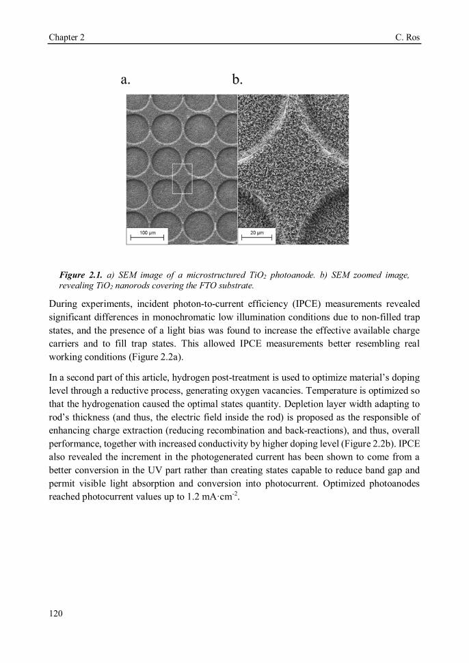
Chapter 2 C. Ros
120
Figure 2.1. a) SEM image of a microstructured TiO2 photoanode. b) SEM zoomed image, revealing TiO2 nanorods covering the FTO substrate.
During experiments, incident photon-to-current efficiency (IPCE) measurements revealed significant differences in monochromatic low illumination conditions due to non-filled trap states, and the presence of a light bias was found to increase the effective available charge carriers and to fill trap states. This allowed IPCE measurements better resembling real working conditions (Figure 2.2a).
In a second part of this article, hydrogen post-treatment is used to optimize material’s doping level through a reductive process, generating oxygen vacancies. Temperature is optimized so that the hydrogenation caused the optimal states quantity. Depletion layer width adapting to rod’s thickness (and thus, the electric field inside the rod) is proposed as the responsible of enhancing charge extraction (reducing recombination and back-reactions), and thus, overall performance, together with increased conductivity by higher doping level (Figure 2.2b). IPCE also revealed the increment in the photogenerated current has been shown to come from a better conversion in the UV part rather than creating states capable to reduce band gap and permit visible light absorption and conversion into photocurrent. Optimized photoanodes reached photocurrent values up to 1.2 mA·cm-2.
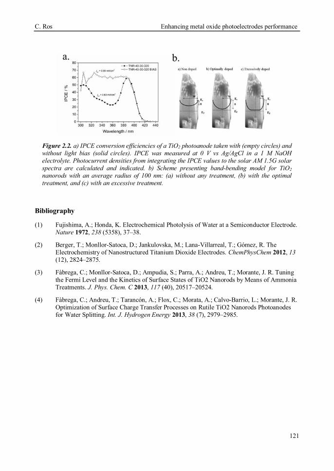
C. Ros Enhancing metal oxide photoelectrodes performance
121
Figure 2.2. a) IPCE conversion efficiencies of a TiO2 photoanode taken with (empty circles) and without light bias (solid circles). IPCE was measured at 0 V vs Ag/AgCl in a 1 M NaOH electrolyte. Photocurrent densities from integrating the IPCE values to the solar AM 1.5G solar spectra are calculated and indicated. b) Scheme presenting band-bending model for TiO2 nanorods with an average radius of 100 nm: (a) without any treatment, (b) with the optimal treatment, and (c) with an excessive treatment.
Bibliography
(1) Fujishima, A.; Honda, K. Electrochemical Photolysis of Water at a Semiconductor Electrode. Nature 1972, 238 (5358), 37–38.
(2) Berger, T.; Monllor-Satoca, D.; Jankulovska, M.; Lana-Villarreal, T.; Gómez, R. The Electrochemistry of Nanostructured Titanium Dioxide Electrodes. ChemPhysChem 2012, 13 (12), 2824–2875.
(3) Fàbrega, C.; Monllor-Satoca, D.; Ampudia, S.; Parra, A.; Andreu, T.; Morante, J. R. Tuning the Fermi Level and the Kinetics of Surface States of TiO2 Nanorods by Means of Ammonia Treatments. J. Phys. Chem. C 2013, 117 (40), 20517–20524.
(4) Fàbrega, C.; Andreu, T.; Tarancón, A.; Flox, C.; Morata, A.; Calvo-Barrio, L.; Morante, J. R. Optimization of Surface Charge Transfer Processes on Rutile TiO2 Nanorods Photoanodes for Water Splitting. Int. J. Hydrogen Energy 2013, 38 (7), 2979–2985.

Chapter 2 C. Ros
122
C. Ros Enhancing metal oxide photoelectrodes performance
123

Chapter 2 C. Ros
124
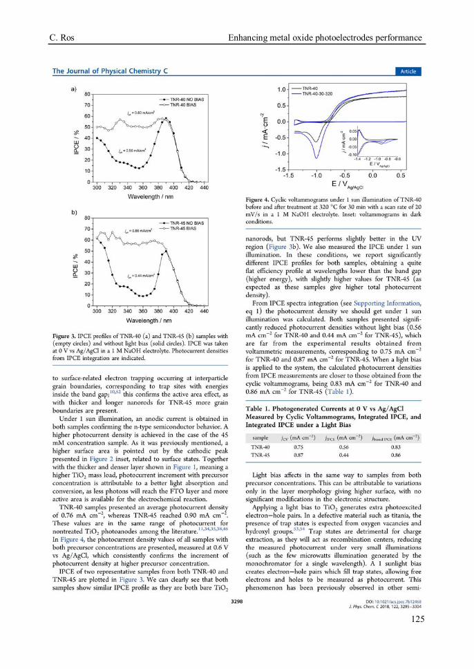
C. Ros Enhancing metal oxide photoelectrodes performance
125
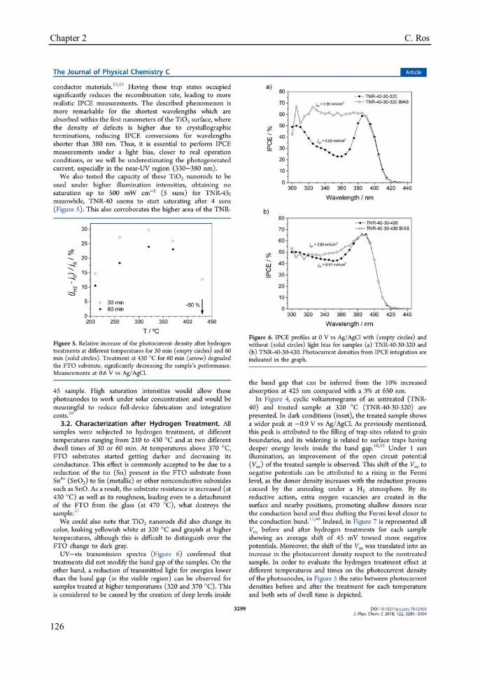
Chapter 2 C. Ros
126

C. Ros Enhancing metal oxide photoelectrodes performance
127
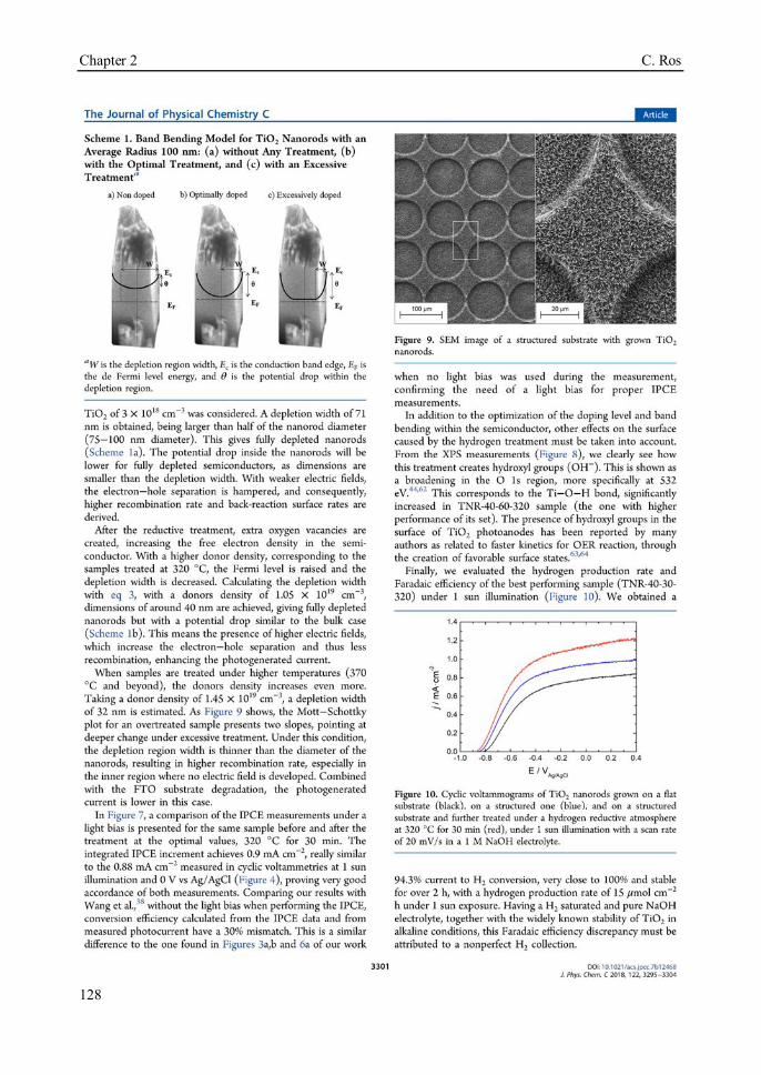
Chapter 2 C. Ros
128
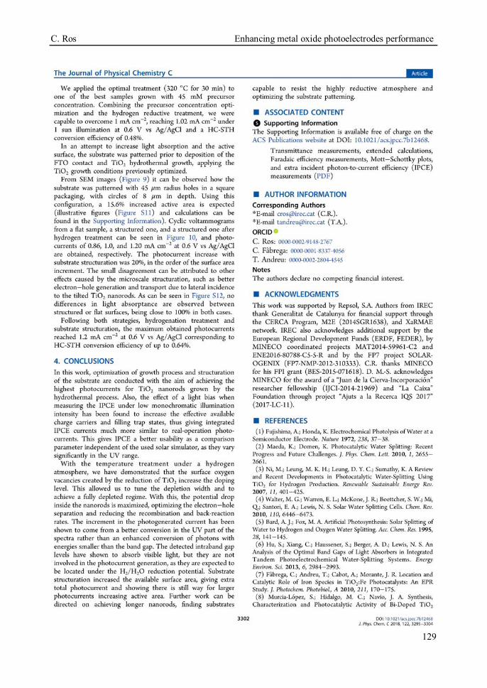
C. Ros Enhancing metal oxide photoelectrodes performance
129
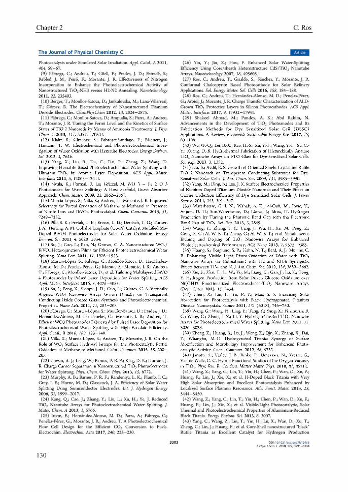
Chapter 2 C. Ros
130

C. Ros Enhancing metal oxide photoelectrodes performance
131

Chapter 2 C. Ros
132

C. Ros Enhancing metal oxide photoelectrodes performance
133

Chapter 2 C. Ros
134
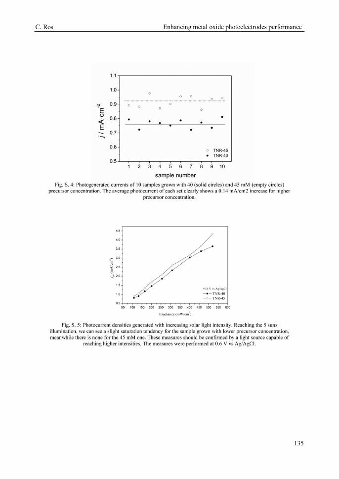
C. Ros Enhancing metal oxide photoelectrodes performance
135

Chapter 2 C. Ros
136
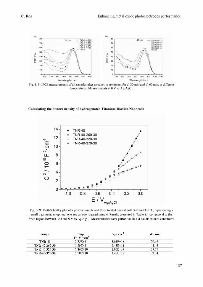
C. Ros Enhancing metal oxide photoelectrodes performance
137

Chapter 2 C. Ros
138
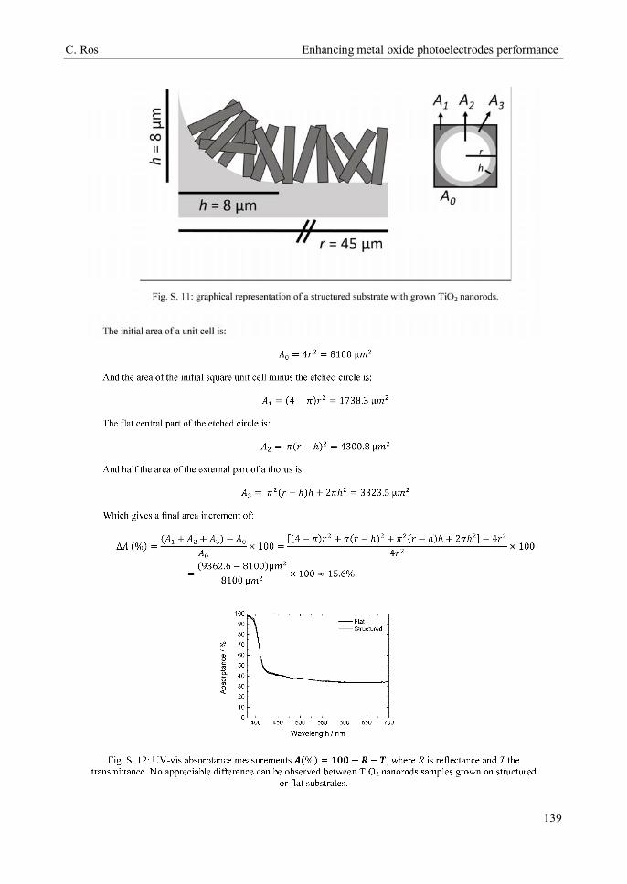
C. Ros Enhancing metal oxide photoelectrodes performance
139

Chapter 2 C. Ros
140

Chapter 3
Titanium dioxide as conductive and protective layer for silicon-based
photocathodes

Chapter 3 C. Ros
142
C. Ros Titanium dioxide as conductive and protective layer for silicon-based photocathodes
143
In previous chapter efforts were put into enhancing the productivity of metal-oxide based photoanodes, but even after extensive research last decades and combining substrate microstructuration, nanorods growth and electronic modifications to the semiconductor, obtained photocurrents were below 2 mA·cm-2. If significant productivities are to be obtained, semiconductors with smaller band gap and more efficient in charge separation and extraction are to be used.
This chapter is focused on implementing silicon p-n junctions to form photocathodes through protecting them from corrosion with ALD-grown TiO2 protective layers. The strategy has been used for some years, as reported in Chapter 1 section 7, where an homojunction in a short band gap material, highly prone for charge separation and transport (resembling already commercial strategies for photovoltaic technologies) is prevented from contacting the corrosive electrolyte by a conductive, transparent and protective layer. This way, the electron-hole generation and charge separation and extraction can be almost independently optimized in the photoabsorber. The protective layer, thus, must only be highly efficient in transparency and conductivity.
TiO2 has been selected as protective layer for its large band gap (3.2 eV), transparent to major part of visible light and its known stability and semiconductor n-type behavior, permitting electron conductivity. ALD has been chosen as deposition technique as it permits high deposition thickness control and conformal coverage of any rugosity, minimizing pinholes which would permit the electrolyte to corrode the substrate1. 100 nm thick layers were selected to assure good protection and to exclude possible tunneling conductivity, thus focusing our analysis on conductivity intrinsic to TiO2. The slow deposition process and its relation with TiO2 layer crystallization will be studied, together with its implications in conductivity and stability.
3.1. Charge transfer characterization of ALD-grown TiO2 protective layers in silicon photocathodes
In the first article included in this chapter, the aim was to elucidate the fabrication parameters of ALD TiO2 layers governing especially conductivity and stability in photocathodic hydrogen evolution. Acidic media was selected as it is more prone for the HER reaction together with platinum as highly efficient catalyst. Silicon was chosen as photoabsorber for our photocathodes (Figure 3.1a), as it has long demonstrated efficient light to current conversion of wide part of the solar spectra, and its p-n homojunction is not sensible to the fabrication steps used in this work. This allowed us a study with an invariant photoabsorber part.
Layers were fabricated at deposition temperatures of 100 to 300 ºC, and characterized, finding significant morphological, crystallographic and conductivity changes. Layers were homogeneous, amorphous and highly resistive at 100 ºC, meanwhile increasing to 200 ºC
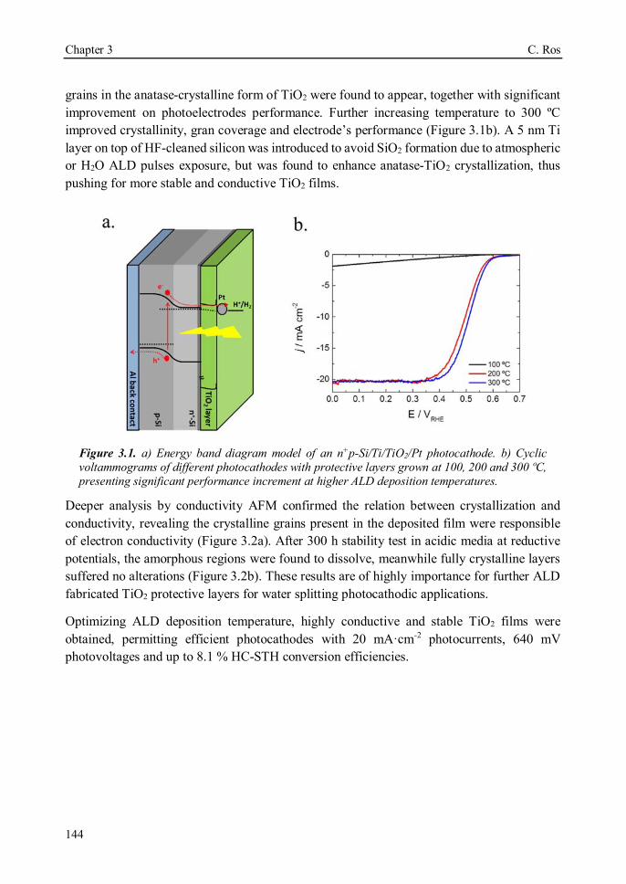
Chapter 3 C. Ros
144
grains in the anatase-crystalline form of TiO2 were found to appear, together with significant improvement on photoelectrodes performance. Further increasing temperature to 300 ºC improved crystallinity, gran coverage and electrode’s performance (Figure 3.1b). A 5 nm Ti layer on top of HF-cleaned silicon was introduced to avoid SiO2 formation due to atmospheric or H2O ALD pulses exposure, but was found to enhance anatase-TiO2 crystallization, thus pushing for more stable and conductive TiO2 films.
Figure 3.1. a) Energy band diagram model of an n+p-Si/Ti/TiO2/Pt photocathode. b) Cyclic voltammograms of different photocathodes with protective layers grown at 100, 200 and 300 ºC, presenting significant performance increment at higher ALD deposition temperatures.
Deeper analysis by conductivity AFM confirmed the relation between crystallization and conductivity, revealing the crystalline grains present in the deposited film were responsible of electron conductivity (Figure 3.2a). After 300 h stability test in acidic media at reductive potentials, the amorphous regions were found to dissolve, meanwhile fully crystalline layers suffered no alterations (Figure 3.2b). These results are of highly importance for further ALD fabricated TiO2 protective layers for water splitting photocathodic applications.
Optimizing ALD deposition temperature, highly conductive and stable TiO2 films were obtained, permitting efficient photocathodes with 20 mA·cm-2 photocurrents, 640 mV photovoltages and up to 8.1 % HC-STH conversion efficiencies.

C. Ros Titanium dioxide as conductive and protective layer for silicon-based photocathodes
145
Figure 3.2. a) Cross section SEM image of a TiO2 layer grown directly on Silicon. Inset: c-AFM map showing conductivity is detected where there is a crystal, and no conductivity on amorphous regions. b) Cross section SEM image of a TiO2 layer after 300 h stability test in acid, presenting dissolution of the amorphous regions.
Bibliography
(1) Mikko Ritala; Markku Leskela. Atomic Layer Epitaxy--a Valuable Tool for Nanotechnology? Nanotechnology 1999, 10, 19–24.

Chapter 3 C. Ros
146
C. Ros Titanium dioxide as conductive and protective layer for silicon-based photocathodes
147
Chapter 3 C. Ros
148
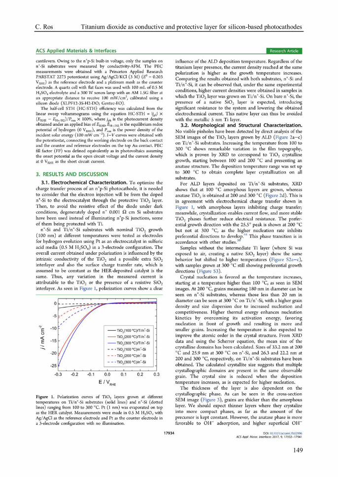
C. Ros Titanium dioxide as conductive and protective layer for silicon-based photocathodes
149

Chapter 3 C. Ros
150

C. Ros Titanium dioxide as conductive and protective layer for silicon-based photocathodes
151

Chapter 3 C. Ros
152

C. Ros Titanium dioxide as conductive and protective layer for silicon-based photocathodes
153
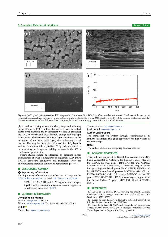
Chapter 3 C. Ros
154
C. Ros Titanium dioxide as conductive and protective layer for silicon-based photocathodes
155

Chapter 3 C. Ros
156
C. Ros Titanium dioxide as conductive and protective layer for silicon-based photocathodes
157
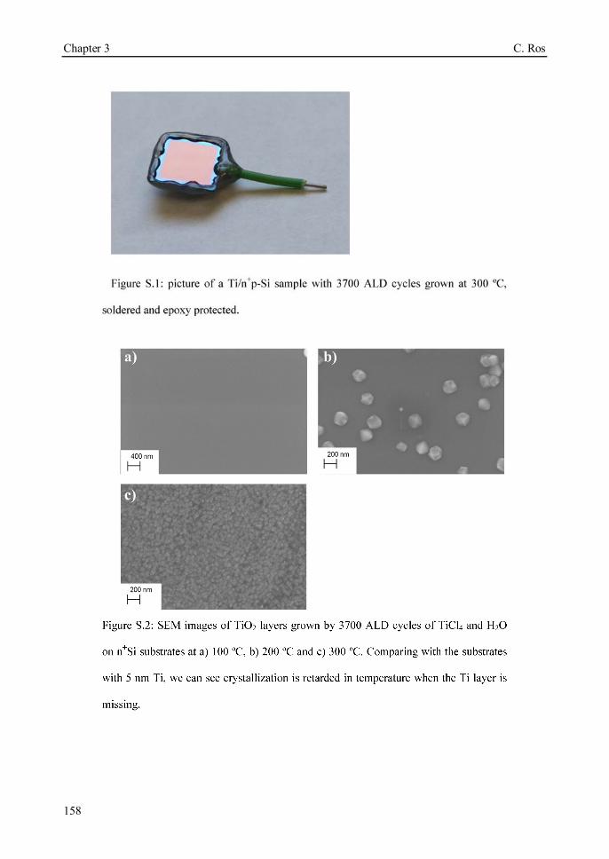
Chapter 3 C. Ros
158
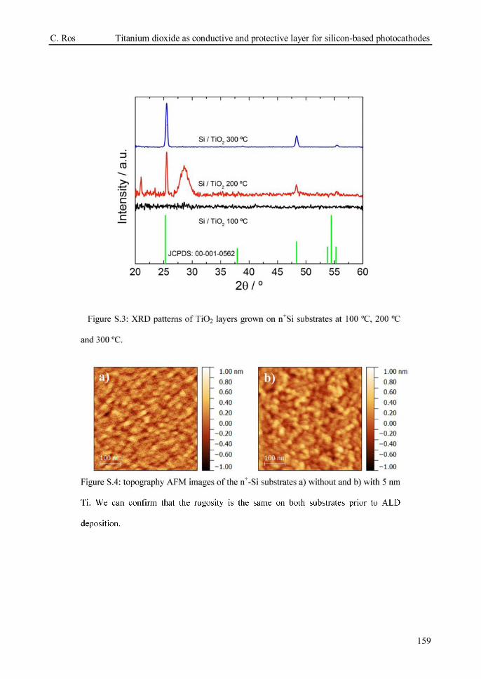
C. Ros Titanium dioxide as conductive and protective layer for silicon-based photocathodes
159
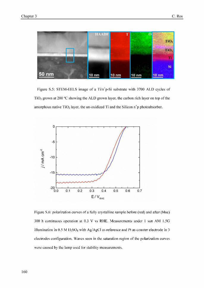
Chapter 3 C. Ros
160
Chapter 4
Adapting protective layers for thin film chalcogenide photoabsorbers

Chapter 4 C. Ros
162
C. Ros Adapting protective layers for thin film chalcogenide photoabsorbers
163
In chapter 3, the titanium dioxide protective films were optimized and characterized using silicon as photoabsorber for photocathodic hydrogen evolution. As was mentioned, silicon could be used as a reference semiconductor thanks to its stability, but other emerging photovoltaic semiconductors1 have shown promising results and present interesting features.
Chalcogenide based photoabsorbers are part of thin film photovoltaic semiconductors, with thicknesses ranging few micrometers thanks to high absorption coefficient and thus, have the possibility to be deposited on glass or on flexible substrates such as steel, aluminum or a polymer, permitting roll-to-roll fabrication2. Thin films permit few material consumption and less fabrication costs, pushing for cheaper devices compared to other photovoltaics while achieving high efficiencies3. Moreover, chalcogenide photoabsorbers electronic structure is defined by a complex structure of Cu vacancies acting as electron acceptors and In, Ga, Se substitutions and defects and, by adapting the elemental ratio, its band gap (and thus, photovoltage/saturating photocurrent) can be significantly modified4.
Among them, CIGS and CZTS have 1.0 to 1.8 eV variable band gaps variating In/Ga or S/Se ratio respectively. CIGS have already been commercialized and have presented about 20% conversion efficiencies3, while CZTS over 10% with only abundant and non-toxic elements (indium and gallium are replaced by zinc and tin)5. The p-n junction is formed normally with n-type CdS or InS ~50 nm layers and ZnO transparent conductive top contact. However, TCO layers are not protective enough against corrosion in acid or alkaline media due to Zn2+ and Sn2+ forming soluble species6 and thus, require further protective layers.
Although, due to the mentioned primordial role of structural imperfections in defining the electronic structure, thermal treatments during late fabrication steps like protective film deposition will significantly influence the photovoltaic efficiency7. Thus, optimal coupling of both technologies is of primordial concern. TiO2 was demonstrated highly stable and conductive for cathodic applications in previous chapter, requiring a crystalline film. For it, ALD is one of the best candidates: thanks to its slow deposition and intermediate species mobility, the necessary TiO2 crystalline structure can be obtained at lower temperatures than other deposition techniques, often requiring ~400 ºC8,9.
4.1. Conformal chalcopyrite based photocathode for solar refinery applications
In the first article of this chapter, chalcopyrite CIGSe/CdS p-n heterojunctions on stainless steel (SS) foil were studied as flexible photocathodes. Due to the known instability of TCO films in acidic conditions, TiO2 protective layers were applied to analyze the possibility of substituting the TCO. Platinum was used as HER catalyst. Both i-ZnO and AZO layers are found to enhance protected photocathodes efficiency by helping in p-n junction charge separation and film conductivity (Figure 4.1).
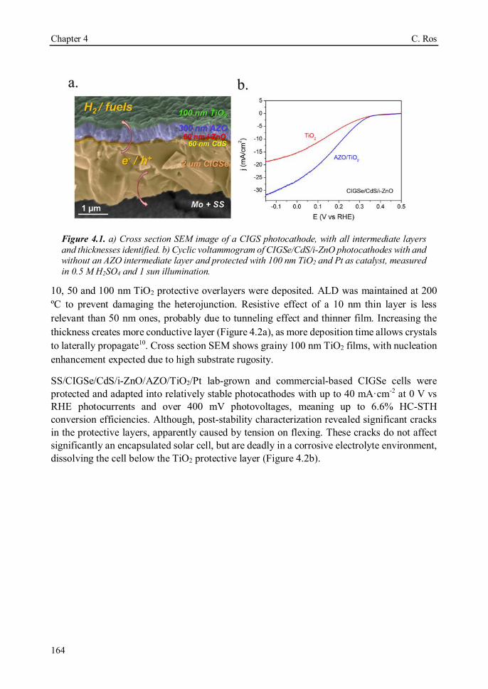
Chapter 4 C. Ros
164
Figure 4.1. a) Cross section SEM image of a CIGS photocathode, with all intermediate layers and thicknesses identified. b) Cyclic voltammogram of CIGSe/CdS/i-ZnO photocathodes with and without an AZO intermediate layer and protected with 100 nm TiO2 and Pt as catalyst, measured in 0.5 M H2SO4 and 1 sun illumination.
10, 50 and 100 nm TiO2 protective overlayers were deposited. ALD was maintained at 200 ºC to prevent damaging the heterojunction. Resistive effect of a 10 nm thin layer is less relevant than 50 nm ones, probably due to tunneling effect and thinner film. Increasing the thickness creates more conductive layer (Figure 4.2a), as more deposition time allows crystals to laterally propagate10. Cross section SEM shows grainy 100 nm TiO2 films, with nucleation enhancement expected due to high substrate rugosity.
SS/CIGSe/CdS/i-ZnO/AZO/TiO2/Pt lab-grown and commercial-based CIGSe cells were protected and adapted into relatively stable photocathodes with up to 40 mA·cm-2 at 0 V vs RHE photocurrents and over 400 mV photovoltages, meaning up to 6.6% HC-STH conversion efficiencies. Although, post-stability characterization revealed significant cracks in the protective layers, apparently caused by tension on flexing. These cracks do not affect significantly an encapsulated solar cell, but are deadly in a corrosive electrolyte environment, dissolving the cell below the TiO2 protective layer (Figure 4.2b).

C. Ros Adapting protective layers for thin film chalcogenide photoabsorbers
165
Figure 4.2. a) Scheme describing the possible conduction paths of a 10 nm TiO2 layer presenting tunneling, a 50 nm one with limited crystal coverage and a 100 nm one, where deposition time gave crystals time to develop and cover significant part of the layer. b) Cross section SEM image of a photocathode after 1h stability, presenting significant cracks and detached film. Inset shows a flexed device.
4.2. Turning earth abundant kesterite-based solar cells into efficient protected water-splitting photocathodes
In this article, the compatibility of ALD-TiO2 layers to protect earth-abundant copper−zinc−tin−chalcogenide (CZTS/Se) kesterite-based devices is studied, as alternative to CIGS that uses indium, limited in availability. Different stoichiometry CZTSe, CZTSSe and CZTS photoabsorbers, with 1.0, 1.15 and 1.5 eV band gaps are fabricated by modifying the chalcogenide S/Se ratio. Following previous article, CdS/i-ZnO/ITO/100 nm TiO2/Pt overlayers were deposited for efficient photovoltaic behavior and charge transfer to the electrolyte (Figure 4.3a).
Chalcogenide kesterites as photoabsorbers show high performance thanks to highly complex structure based on specific phases, lattice parameters, elemental substitution and diffusion and defects distribution, sensible to few hundred Celsius7. Temperature-caused alterations on kesterite electronic structure were studied by variating TiO2 deposition temperature from 200 to 300 ºC. As can be observed in Figure 4.3b, 200 ºC is the maximum before significantly affecting the CIGSe/CdS junction performance, and over one hour stability was obtained thanks to the TiO2 protective film. ALD was proven as one of the few techniques capable of protecting kesterite chalcogenides thanks to the low crystallization temperature.
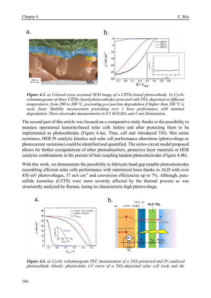
Chapter 4 C. Ros
166
Figure 4.3. a) Colored cross sectional SEM image of a CZTSe-based photocathode. b) Cyclic voltammograms of three CZTSe-based photocathodes protected with TiO2 deposited at different temperatures, from 200 to 300 ºC, presenting p-n junction degradation if higher than 200 ºC is used. Inset: Stability measurement presenting over 1 hour performance with minimal degradation. Three electrodes measurements in 0.5 M H2SO4 and 1 sun illumination.
The second part of this article was focused on a comparative study thanks to the possibility to measure operational kesterite-based solar cells before and after protecting them to be implemented as photocathodes (Figure 4.4a). Thus, cell and introduced TiO2 film series resistance, HER Pt catalytic kinetics and solar cell performance alterations (photovoltage or photocurrent variations) could be identified and quantified. The series-circuit model proposed allows for further extrapolations of other photoabsorbers, protective layer materials or HER catalysts combinations in the pursuit of best coupling tandem photoelectrodes (Figure 4.4b).
With this work, we demonstrate the possibility to fabricate band gap tunable photoelectrodes resembling efficient solar cells performance with minimized loses thanks to ALD with over 450 mV photovoltages, 37 mA·cm-2 and conversion efficiencies up to 7%. Although, pure-sulfide kesterites (CZTS) were more severely affected by the thermal process as was structurally analyzed by Raman, losing its characteristic high photovoltage.
Figure 4.4. a) Cyclic voltammogram PEC measurement of a TiO2-protected and Pt catalyzed photocathode (black), photovoltaic I-V curve of a TiO2-deposited solar cell (red) and the

C. Ros Adapting protective layers for thin film chalcogenide photoabsorbers
167
calculated HER behavior of the Pt catalyst by subtracting the black curve to the red one (in blue). b) Scheme of the full photocathode electric series circuit presenting all the calculated electrical elements.
Bibliography
(1) Polman, A.; Knight, M.; Garnett, E. C.; Ehrler, B.; Sinke, W. C.; Summary, R.; Polman, A.; Knight, M.; Garnett, E. C.; Ehrler, B.; et al. Photovoltaic Materials – Present Efficiencies and Future Challenges. Science (80-. ). 2016, 352 (6283), 307.
(2) Izquierdo-Roca, V.; Caballero, R.; Fontané, X.; Kaufmann, C. A.; Álvarez-García, J.; Calvo-Barrio, L.; Saucedo, E.; Pérez-Rodríguez, A.; Morante, J. R.; Schock, H. W. Raman Scattering Analysis of Cu-Poor Cu(In,Ga)Se2 Cells Fabricated on Polyimide Substrates: Effect of Na Content on Microstructure and Phase Structure. Thin Solid Films 2011, 519 (21), 7300–7303.
(3) Repins, I.; Contreras, M. A.; Egaas, B.; DeHart, C.; Scharf, J.; Perkins, C. L.; To, B.; Noufi, R. 19.9%-Efficient ZnO/CdS/CuInGaSe2 Solar Cell with 81.2% Fill Factor. Prog. Photovoltaics Res. Appl. 2008, 16 (3), 235–239.
(4) Dimitrievska, M.; Fairbrother, A.; Saucedo, E.; Pérez-Rodríguez, A.; Izquierdo-Roca, V. Secondary Phase and Cu Substitutional Defect Dynamics in Kesterite Solar Cells: Impact on Optoelectronic Properties. Sol. Energy Mater. Sol. Cells 2016, 149, 304–309.
(5) Wang, W.; Winkler, M. T.; Gunawan, O.; Gokmen, T.; Todorov, T. K.; Zhu, Y.; Mitzi, D. B. Device Characteristics of CZTSSe Thin-Film Solar Cells with 12.6% Efficiency. Adv. Energy Mater. 2014, 4 (7), 1–5.
(6) Awan, I. Z.; Khan, A. Q.; Awan, I. Z.; Khan, A. Q.; Nationale, E.; Chimie, S. De. Corrosion – Occurrence & Prevention. 2018, 40 (04), 602–655.
(7) Neuschitzer, M.; Sanchez, Y.; Olar, T.; Thersleff, T.; Lopez-Marino, S.; Oliva, F.; Espindola-Rodriguez, M.; Xie, H.; Placidi, M.; Izquierdo-Roca, V.; et al. Complex Surface Chemistry of Kesterites: Cu/Zn Reordering after Low Temperature Postdeposition Annealing and Its Role in High Performance Devices. Chem. Mater. 2015, 27 (15), 5279–5287.
(8) Mei, B.; Pedersen, T.; Malacrida, P.; Bae, D.; Frydendal, R.; Hansen, O.; Vesborg, P. C. K.; Seger, B.; Chorkendorff, I. Crystalline TiO 2 : A Generic and Effective Electron-Conducting Protection Layer for Photoanodes and -Cathodes. J. Phys. Chem. C 2015, 119 (27), 15019–15027.
(9) Malizia, M.; Seger, B.; Chorkendorff, I.; Vesborg, P. C. K. Formation of a P-n Heterojunction on GaP Photocathodes for H2 Production Providing an Open-Circuit Voltage of 710 MV. J. Mater. Chem. A 2014, 2 (19), 6847–6853.
(10) Miikkulainen, V.; Leskelä, M.; Ritala, M.; Puurunen, R. L.; Leskelä, M.; Ritala, M.; Puurunen, R. L. Crystallinity of Inorganic Films Grown by Atomic Layer Deposition: Overview and General Trends. J. Appl. Phys. 2013, 113 (2), 021301.

Chapter 4 C. Ros
168
C. Ros Adapting protective layers for thin film chalcogenide photoabsorbers
169
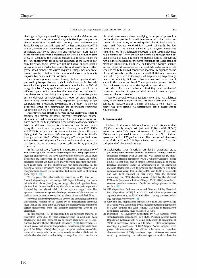
Chapter 4 C. Ros
170

C. Ros Adapting protective layers for thin film chalcogenide photoabsorbers
171

Chapter 4 C. Ros
172
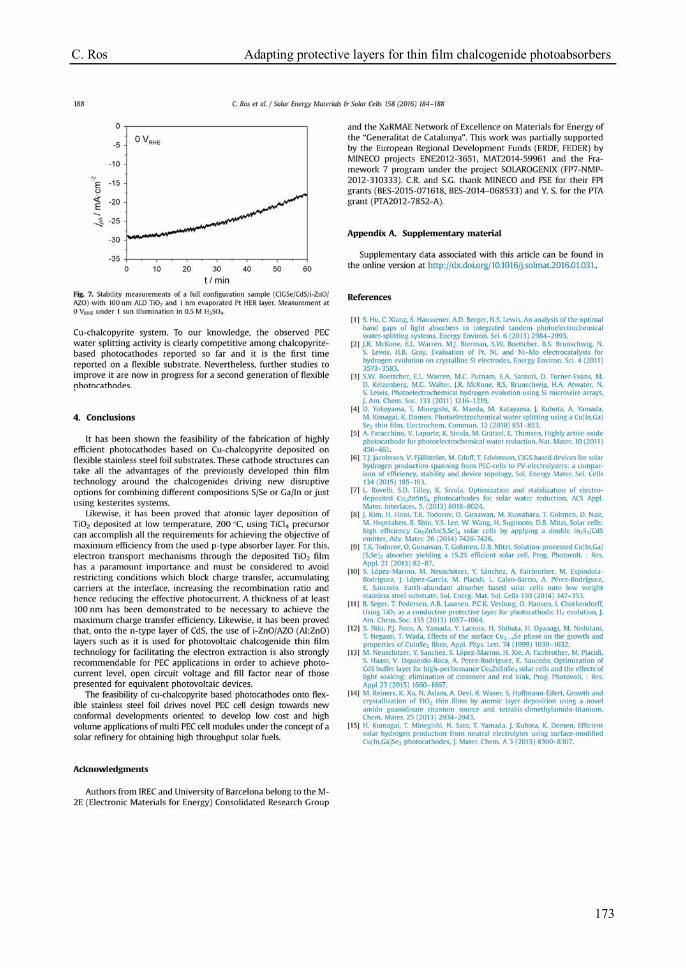
C. Ros Adapting protective layers for thin film chalcogenide photoabsorbers
173
Chapter 4 C. Ros
174
Supplementary Data
Conformal chalcopyrite based photocathode for solar refinery applications
Carles Rosa, Teresa Andreua,*, Sergio Giraldoa, Yudania Sáncheza, Joan Ramon Morantea,b,*
a Catalonia Institute for Energy Research, IREC. Jardins de les Dones de Negre 1, 08930
Sant Adrià de Besòs, Barcelona, Spain
b Departament d’Electrònica, Universitat de Barcelona, Martí i Franquès, 1, 08028
Barcelona, Spain
* Corresponding author: Teresa Andreu, Joan Ramon Morante
Electronic mail: [email protected]; [email protected]
Ph.: +34 933562615
Fax: +34 933563802

C. Ros Adapting protective layers for thin film chalcogenide photoabsorbers
175
Figure S1. XRD pattern of the TiO2 ALD deposited layer morphology on silicon substrate.
Red vertical lines corresponds to JCPDS card 1-0562 (anatase).
Figure S2: AFM images (conductive tip) of a 200 ºC grown TiO2 ALD layer on an n+-Si
substrate. Topography image (left) and intensity image (right).

Chapter 4 C. Ros
176
C. Ros Adapting protective layers for thin film chalcogenide photoabsorbers
177
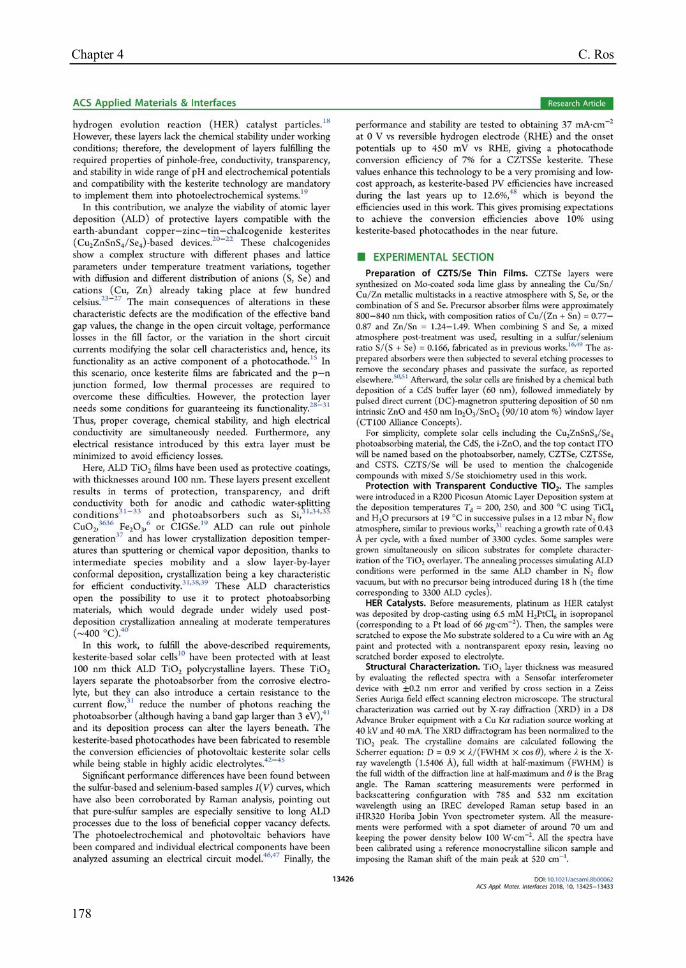
Chapter 4 C. Ros
178
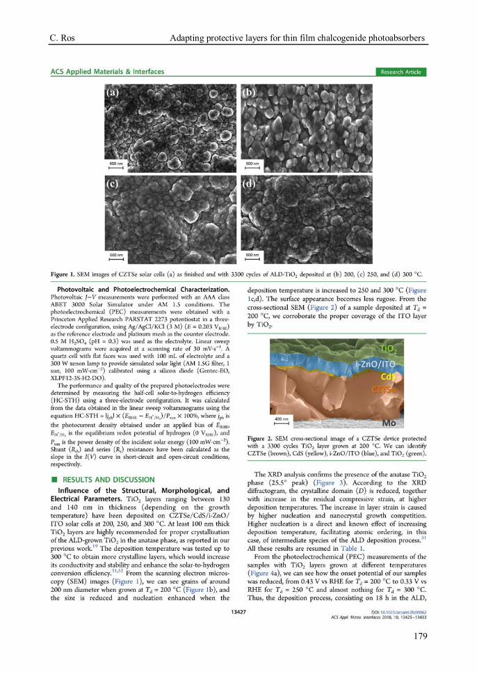
C. Ros Adapting protective layers for thin film chalcogenide photoabsorbers
179
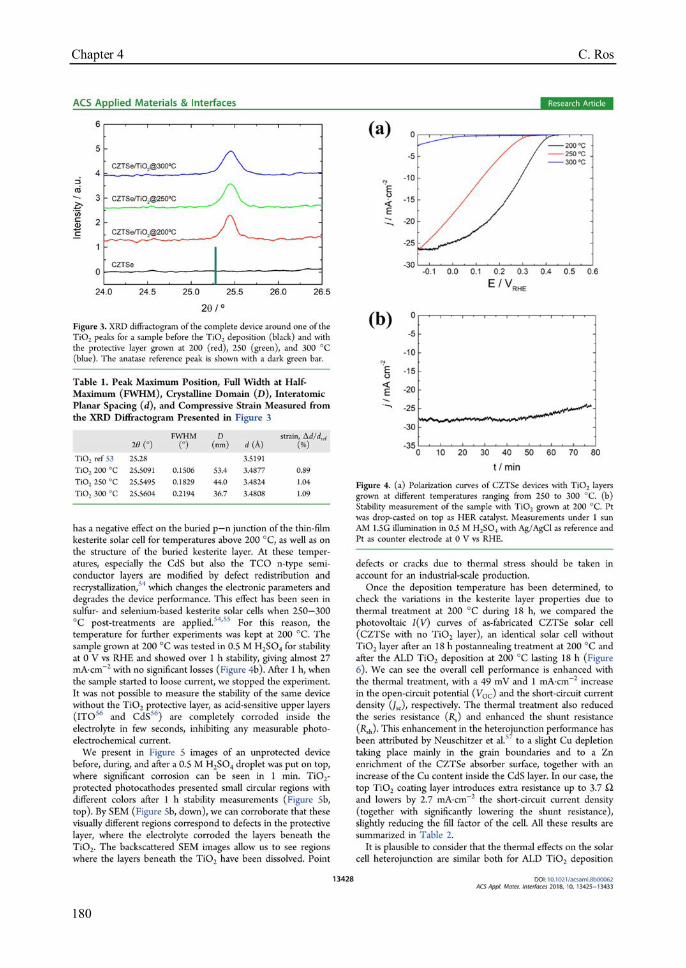
Chapter 4 C. Ros
180
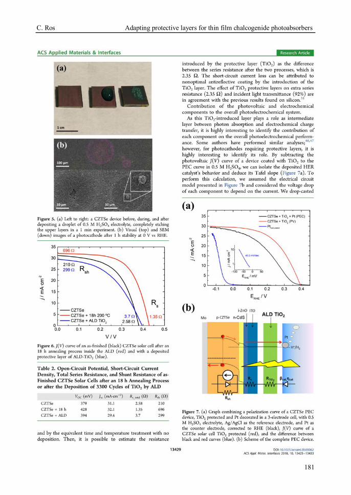
C. Ros Adapting protective layers for thin film chalcogenide photoabsorbers
181

Chapter 4 C. Ros
182
C. Ros Adapting protective layers for thin film chalcogenide photoabsorbers
183
Chapter 4 C. Ros
184
C. Ros Adapting protective layers for thin film chalcogenide photoabsorbers
185

Chapter 4 C. Ros
186
Chapter 5 Conductivity and endurance of
protective layers in alkaline anodic conditions

Chapter 5 C. Ros
188
C. Ros Conductivity and endurance of protective layers in alkaline anodic conditions
189
In this chapter, focus is put into protective layers for photoanodes in alkaline electrolytes, more prone for the OER reaction. Silicon as photoabsorber has been previously studied and used as reference material in chapter 3 thanks to the high performance and not being affected by post-treatments at few hundred Celsius as they are fabricated at ~1000 ºC1. In addition, as was discussed in chapter 1 section 4, alkaline electrolytes corrode silicon with significant anisotropic etching dissolution, thus corrosion can be observed and used to characterize the protective capacity of the overlayers.
Silicon is a highly versatile semiconductor. A p-n junction designed so that the HER or OER are performed on its frontal side only requires inverting the n or p-type extrinsic doping order. By using n-type wafers with a p+ top region, holes are conducted to the electrolyte. Protective layers thus should be favorable to hole conduction and energetically aligned to avoid forming any detrimental barrier with p+-Si or the OER electrocatalyst. Although, this is not the only way1.
Two strategies were followed in this article, both using ALD thanks to its minimal-pinholes, layer thickness control and low deposition temperatures, among others. The first one is using TiO2, an n-type semiconductor proven with some works to be highly conductive for anodic current, and with scientific debate on which is the specific conductivity mechanism. NiFe-based catalysts will be used. The second one is based on NiO protective layers, a p-type semiconductor that forms, in contact with alkaline electrolytes, favorable oxyhydroxides highly catalytic to the OER.
5.1. Insight into the degradation mechanisms of atomic layer deposited TiO2 as photoanode protective layer
In the first article of this chapter, n-type TiO2 as protective layer for silicon photoanodes in alkaline electrolytes is characterized. Two aspects are studied: first, the conductivity mechanism, considered mid-band gap states mediated hole conductivity through amorphous TiO2 in some works2 or conduction band electron transport in crystals in others1, and the second is the stability of these oxygen-defective layers in highly oxidative electrolytes and potentials.
ALD wide temperature window is used to fabricate completely amorphous layers (deposited at 100 ºC), and partially crystalline (150 ºC) and fully crystalline ones (300 ºC) on p+n-Si photoelectrodes and further 5 nm NiFe decorated. PEC measurements revealed strong correlation of performance and deposition temperature, with no photocurrent at 100 ºC and significant photodiode saturation of >20 mA·cm-2 at 300 ºC (Figure 5.1a). HRTEM and Raman characterization revealed multicrystalline TiO2 grains at already 150 ºC deposition temperatures (Figure 5.2b), and c-AFM maps showed preferential conductivity regions only in the crystalline parts.
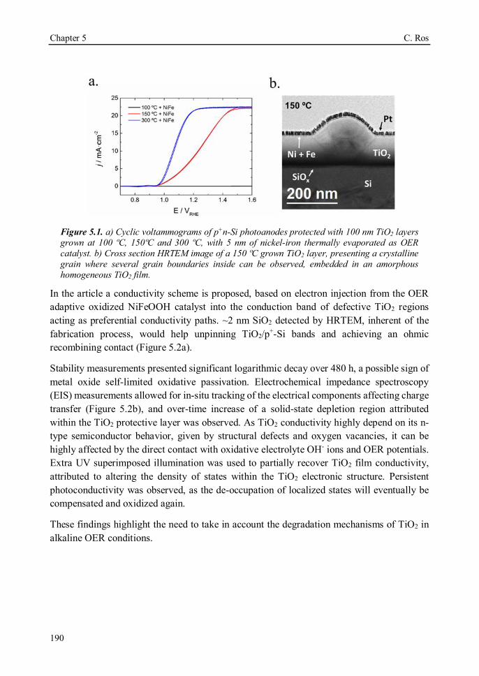
Chapter 5 C. Ros
190
Figure 5.1. a) Cyclic voltammograms of p+n-Si photoanodes protected with 100 nm TiO2 layers grown at 100 ºC, 150ºC and 300 ºC, with 5 nm of nickel-iron thermally evaporated as OER catalyst. b) Cross section HRTEM image of a 150 ºC grown TiO2 layer, presenting a crystalline grain where several grain boundaries inside can be observed, embedded in an amorphous homogeneous TiO2 film.
In the article a conductivity scheme is proposed, based on electron injection from the OER adaptive oxidized NiFeOOH catalyst into the conduction band of defective TiO2 regions acting as preferential conductivity paths. ~2 nm SiO2 detected by HRTEM, inherent of the fabrication process, would help unpinning TiO2/p+-Si bands and achieving an ohmic recombining contact (Figure 5.2a).
Stability measurements presented significant logarithmic decay over 480 h, a possible sign of metal oxide self-limited oxidative passivation. Electrochemical impedance spectroscopy (EIS) measurements allowed for in-situ tracking of the electrical components affecting charge transfer (Figure 5.2b), and over-time increase of a solid-state depletion region attributed within the TiO2 protective layer was observed. As TiO2 conductivity highly depend on its n-type semiconductor behavior, given by structural defects and oxygen vacancies, it can be highly affected by the direct contact with oxidative electrolyte OH- ions and OER potentials. Extra UV superimposed illumination was used to partially recover TiO2 film conductivity, attributed to altering the density of states within the TiO2 electronic structure. Persistent photoconductivity was observed, as the de-occupation of localized states will eventually be compensated and oxidized again.
These findings highlight the need to take in account the degradation mechanisms of TiO2 in alkaline OER conditions.
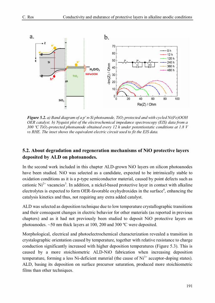
C. Ros Conductivity and endurance of protective layers in alkaline anodic conditions
191
Figure 5.2. a) Band diagram of a p+n-Si photoanode, TiO2 protected and with cycled Ni(Fe)OOH OER catalyst. b) Nyquist plot of the electrochemical impedance spectroscopy (EIS) data from a 300 ºC TiO2-protected photoanode obtained every 12 h under potentiostatic conditions at 1.8 V vs RHE. The inset shows the equivalent electric circuit used to fit the EIS data.
5.2. About degradation and regeneration mechanisms of NiO protective layers deposited by ALD on photoanodes.
In the second work included in this chapter ALD-grown NiO layers on silicon photoanodes have been studied. NiO was selected as a candidate, expected to be intrinsically stable to oxidation conditions as it is a p-type semiconductor material, caused by point defects such as cationic Ni2+ vacancies3. In addition, a nickel-based protective layer in contact with alkaline electrolytes is expected to form OER-favorable oxyhydroxides in the surface4, enhancing the catalysis kinetics and thus, not requiring any extra added catalyst.
ALD was selected as deposition technique due to low temperature crystallographic transitions and their consequent changes in electric behavior for other materials (as reported in previous chapters) and as it had not previously been studied to deposit NiO protective layers on photoanodes. ~50 nm thick layers at 100, 200 and 300 ºC were deposited.
Morphological, electrical and photoelectrochemical characterization revealed a transition in crystalographic orientation caused by temperature, together with relative resistance to charge conduction significantly increased with higher deposition temperatures (Figure 5.3). This is caused by a more stoichiometric ALD-NiO fabrication when increasing deposition temperature, forming a less Ni-deficient material (the cause of Ni3+ acceptor-doping states). ALD, basing its deposition on surface precursor saturation, produced more stoichiometric films than other techniques.

Chapter 5 C. Ros
192
Figure 5.3. a) Cyclic voltammograms of silicon photoanodes ALD-protected with NiO deposited at 100, 200 and 300 ºC showing significantly higher performance at low deposition temperatures. b) Corresponding XRD patterns of NiO films where the same crystalline structure is observed with a change in the orientation between 100 and 200 ºC.
Thanks to the very high conformal deposition of ALD, minimal etched sites caused by pinholes were detected after over 1000 h of >10 mA·cm-2 continuous oxygen evolution in 1 M KOH. Deactivation was detected over several tens of hours, although with periodical cycling a regeneration was possible, proving exceptional protection capabilities of NiO layers (Figure 5.4).
Figure 5.4. a) Stability measurement of a silicon photoanode protected at 100 ºC performed under 1 sun illumination and 1 M KOH as electrolyte. Cyclic voltammograms were performed during the stability at different intervals, temporally recovering the performance of the photoelectrode. b) SEM images of the same photoelectrode after 1000 h stability in 1 M KOH, presenting very few etched sites, related to pinholes caused by defects present during fabrication.

C. Ros Conductivity and endurance of protective layers in alkaline anodic conditions
193
Bibliography
(1) Mei, B.; Pedersen, T.; Malacrida, P.; Bae, D.; Frydendal, R.; Hansen, O.; Vesborg, P. C. K.; Seger, B.; Chorkendorff, I. Crystalline TiO 2 : A Generic and Effective Electron-Conducting Protection Layer for Photoanodes and -Cathodes. J. Phys. Chem. C 2015, 119 (27), 15019–15027.
(2) Sivula, K. Defects Give New Life to an Old Material: Electronically Leaky Titania as a Photoanode Protection Layer. ChemCatChem 2014, 2796–2797.
(3) Nachman, M.; Cojocaru, L. N.; Rîbco, L. V. Electrical Properties of Non‐Stoichiometric Nickel Oxide. Phys. Status Solidi 1965, 8 (3), 773–783.
(4) Dette, C.; Hurst, M. R.; Deng, J.; Nellist, M. R.; Boettcher, S. W. Structural Evolution of Metal (Oxy)Hydroxide Nanosheets during the Oxygen Evolution Reaction. 2018.

Chapter 5 C. Ros
194

C. Ros Conductivity and endurance of protective layers in alkaline anodic conditions
195

Chapter 5 C. Ros
196

C. Ros Conductivity and endurance of protective layers in alkaline anodic conditions
197

Chapter 5 C. Ros
198
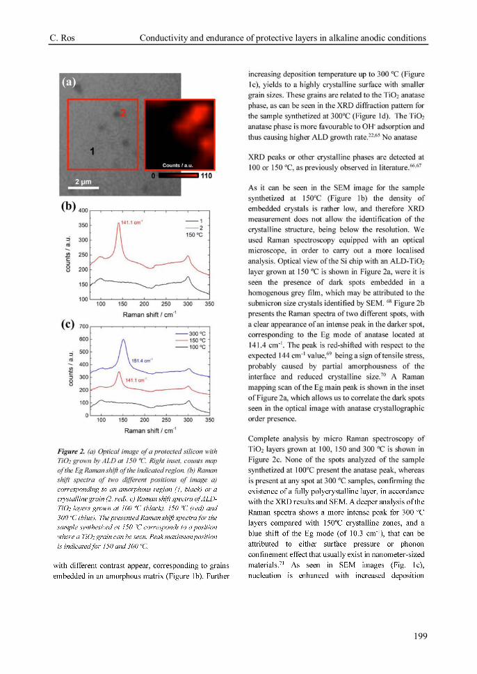
C. Ros Conductivity and endurance of protective layers in alkaline anodic conditions
199
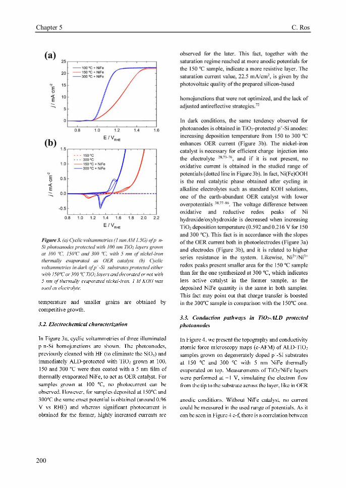
Chapter 5 C. Ros
200

C. Ros Conductivity and endurance of protective layers in alkaline anodic conditions
201
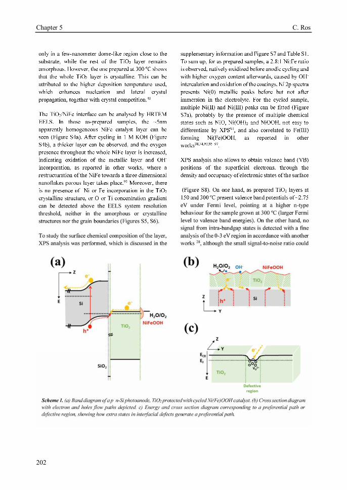
Chapter 5 C. Ros
202
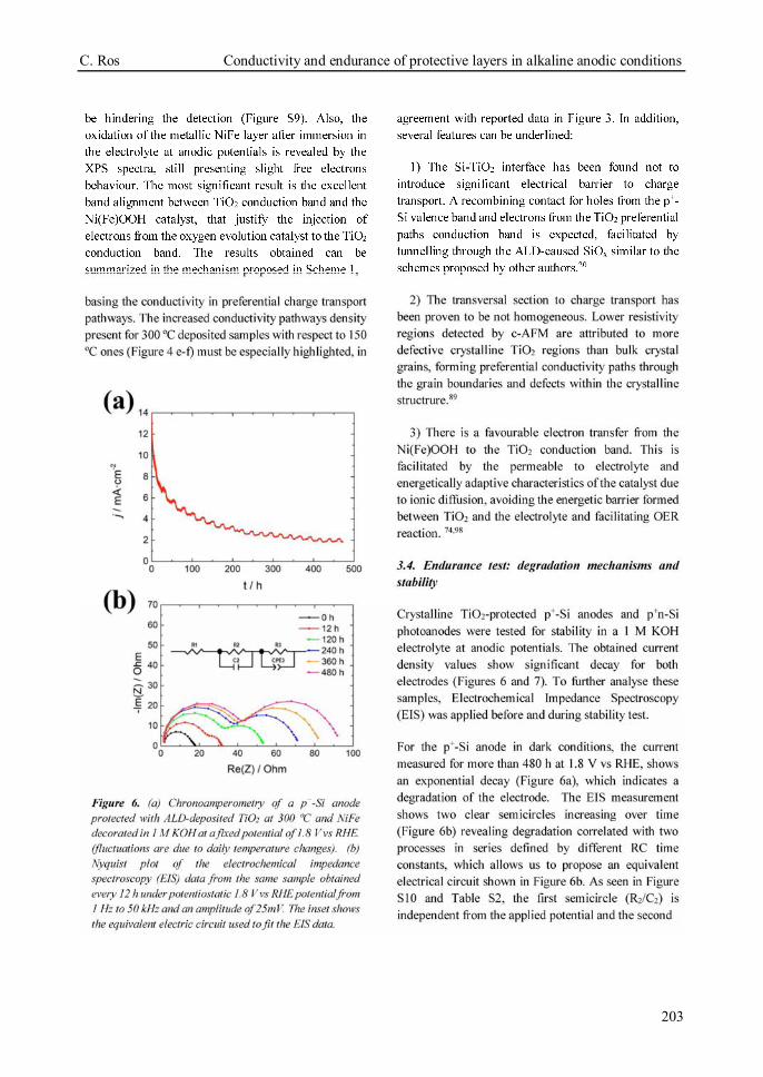
C. Ros Conductivity and endurance of protective layers in alkaline anodic conditions
203

Chapter 5 C. Ros
204
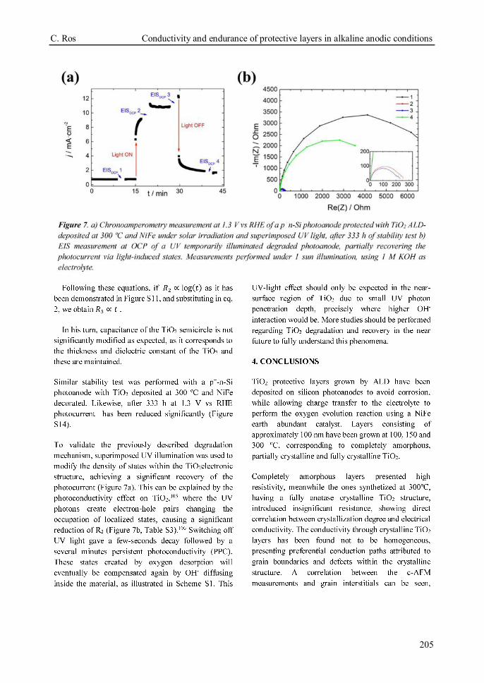
C. Ros Conductivity and endurance of protective layers in alkaline anodic conditions
205
Chapter 5 C. Ros
206
C. Ros Conductivity and endurance of protective layers in alkaline anodic conditions
207
Chapter 5 C. Ros
208
C. Ros Conductivity and endurance of protective layers in alkaline anodic conditions
209
Chapter 5 C. Ros
210

C. Ros Conductivity and endurance of protective layers in alkaline anodic conditions
211
Chapter 5 C. Ros
212
Supplementary Information
Insight into the degradation mechanisms of Atomic
Layer Deposited TiO2 as photoanode protective layer.
Carles Rosa,*, Nina M. Carretero a, Jeremy David c, Jordi Arbiol c,d, Teresa Andreu a,*, Joan R.
Morante a,b
a Catalonia Institute for Energy Research (IREC). Jardins de les Dones de Negre 1, 08930 Sant Adrià
del Besòs, Barcelona, Spain
b Universitat de Barcelona (UB), Martí i Franquès, 1, 08028 Barcelona, Spain
c Catalan Institute of Nanoscience and Nanotechnology (ICN2), CSIC and BIST, Campus UAB,
Bellaterra, 08193 Barcelona, Spain
d ICREA, Pg. Lluís Companys 23, 08010 Barcelona, Spain

C. Ros Conductivity and endurance of protective layers in alkaline anodic conditions
213
Figure S1. Picture of a n+p-Si photoanode presenting the 1.2 x 1.2 cm2 Si chip with an active area of 1
x 1 cm2, defined by a perimeter of 100 nm of SiO2 thick insulator layer. The Si chip was protected by
TiO2-ALD and Ag paint soldered to a Cu wire, and further encapsulated with epoxy resin.
Figure S2. AFM height map of TiO2 + NiFe layers grown at 150 ºC (a, b, e, f) and 300 ºC (c, d, g, g)),
and its respective current intensity maps, at potentials of 1 (e, h) and 1.5 V (f, g) in different sample
regions.
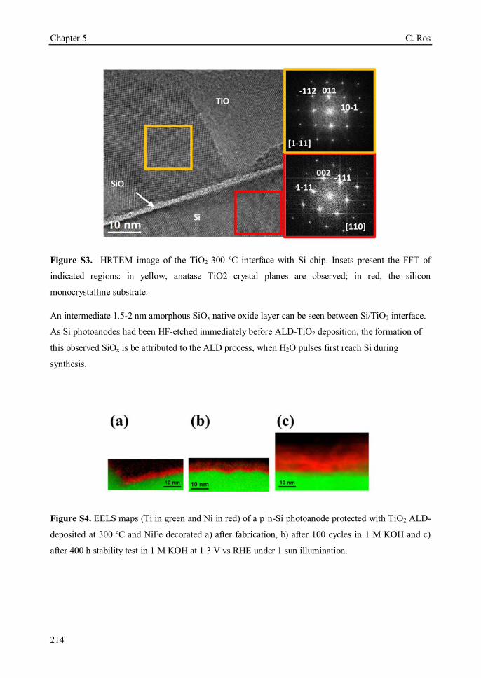
Chapter 5 C. Ros
214
Figure S3. HRTEM image of the TiO2-300 ºC interface with Si chip. Insets present the FFT of
indicated regions: in yellow, anatase TiO2 crystal planes are observed; in red, the silicon
monocrystalline substrate.
An intermediate 1.5-2 nm amorphous SiOx native oxide layer can be seen between Si/TiO2 interface.
As Si photoanodes had been HF-etched immediately before ALD-TiO2 deposition, the formation of
this observed SiOx is be attributed to the ALD process, when H2O pulses first reach Si during
synthesis.
Figure S4. EELS maps (Ti in green and Ni in red) of a p+n-Si photoanode protected with TiO2 ALD-
deposited at 300 ºC and NiFe decorated a) after fabrication, b) after 100 cycles in 1 M KOH and c)
after 400 h stability test in 1 M KOH at 1.3 V vs RHE under 1 sun illumination.
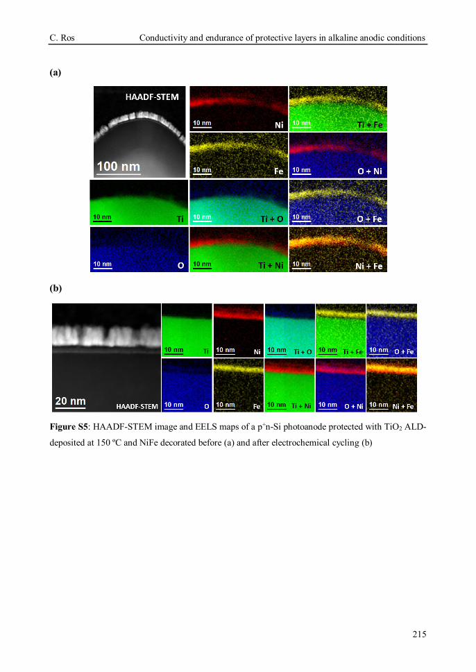
C. Ros Conductivity and endurance of protective layers in alkaline anodic conditions
215
(a)
(b)
Figure S5: HAADF-STEM image and EELS maps of a p+n-Si photoanode protected with TiO2 ALD-
deposited at 150 ºC and NiFe decorated before (a) and after electrochemical cycling (b)
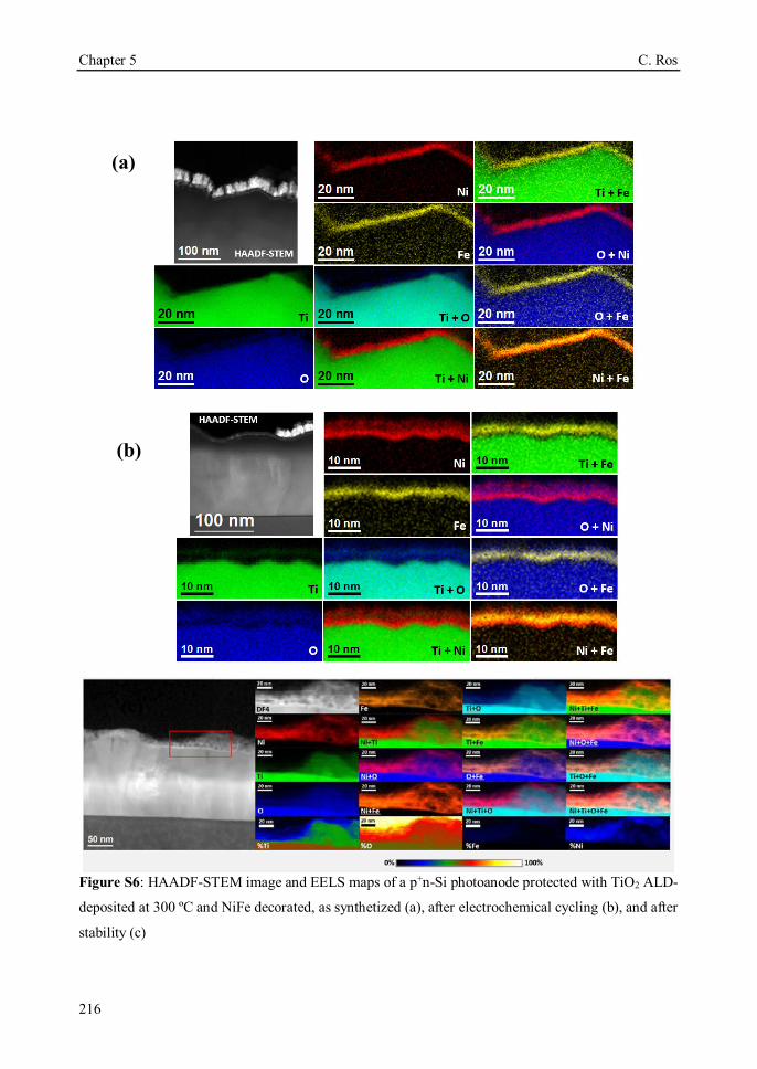
Chapter 5 C. Ros
216
Figure S6: HAADF-STEM image and EELS maps of a p+n-Si photoanode protected with TiO2 ALD-
deposited at 300 ºC and NiFe decorated, as synthetized (a), after electrochemical cycling (b), and after
stability (c)
(a)
(b)
(c)

C. Ros Conductivity and endurance of protective layers in alkaline anodic conditions
217
XPS analysis.
Table S1: XPS detection percentage of selected elements for photoanodes with different ALD growth temperature and NiFe decorated, as prepared and after cycling in 1 M KOH.
C1s (%) O1s (%) Ti2p (%) Fe2p (%) Ni2p (%)
150 ºC + NiFe 52.47 34.09 0.19 3.13 10.12
150 ºC + NiFe cycled 39.93 41.5 0.35 4.93 13.29
300 ºC + NiFe 47.75 35.89 0.37 4.67 11.32
300 ºC + NiFe cycled 35.56 45.56 0.47 4.95 13.46
The catalyst presents an average Ni:Fe ratio of 2.8:1. An increase of the oxygen content can be detected
after cycling, pointing at oxidation of the catalyst layer by the alkaline electrolyte, OH- intercalation
and the anodic electrochemical potentials applied during cycling, corroborating the previous results
obtained by HRTEM and EELS.

Chapter 5 C. Ros
218
Figure S7. XPS spectra of samples with 150 ºC and 300 ºC deposited TiO2 layers and NiFe catalyst as prepared and after cycling in 1 M KOH of a) Ni 2p b) Fe 2p c) O 1s and d) Ti 2p peaks.
Analyzing the electronic core-level photoemission peaks more in detail, significant differences are
observed for samples with TiO2 deposition temperatures of 150 and 300 ºC and after cycling them in 1
M KOH (Figure S7).
Analyzing the Ni2p3/2 peak, we can observe at bonding energy of ~853 eV the presence of the Ni(0)
metallic peak in the samples as prepared, which indicates the incomplete native oxidation caused by
atmospheric oxygen1 and completely disappearing after cycling, which indicates complete oxidation,
also corroborated by the increase in the Ni(II) and Ni(III) peaks (~ 856.2 eV). Apart from this, fitting
the Ni2p peaks to a specific Ni(II) or Ni(III) chemical state is difficult, as NiO, Ni(OH)2, and NiOOH
share various peak energies2, but differ on the ratio between these peaks3. The high percentage detected
for the peak at ~856.2 eV (> 40%) correlated with Ni(OH)2/NiO/NiOOH species, demonstrates that
most probably, the catalytic film is composed of all of these chemical states4,5.
C. Ros Conductivity and endurance of protective layers in alkaline anodic conditions
219
Concerning the Fe2p3/2 peak, there is no presence of metallic iron, and the signal can be attributed to
Fe (III) species as the binding energy is around 711,5 eV, and for Fe(II) species this value is lower.
After cycling, peaks suffer a slight shift towards higher energies (~0.5 eV). The signal-to-noise ratio,
although showing Fe(III) peaks, does not allow us to differentiate between NiFe2O4, FeOOH or
Fe2O36,7. As Fe is almost 3 times less abundant than Ni in these samples, all of it can be expected to be
intercalated forming mostly Ni(Fe)OOH.
O1s signal is mainly attributed either to Ni or Fe coordination. Two clear peaks can be seen for
uncycled samples, one corresponding to metal oxides (~529.5 eV) and another one which could be
ascribed to metal hydroxides (~531.5 eV)3. In the cycled samples, a third peak is detected at 533.1 eV,
which is attributed to physisorbed water (533.5 eV)3. Also, the hydroxide peak becomes much more
predominant over the oxides, as it should be expected1,6, together with absolute higher oxygen content
detected, caused by the oxidation of the metallic Ni-Fe and the corresponding OH intercalation.
Regarding the Ti2p peaks of all samples, the main peak at ~458.7 eV can be attributed to the Ti (IV)
2p3/2 with the corresponding 2p1/2 peak at 464.3 eV8.
Valence Band Studies. After 5 nm NiFe coating is thermally evaporated on top of TiO2 grown at 150
and 300 ºC, metallic behaviour is detected. NiFe layer before cycling has mainly a metallic nature with
a partial contribution of a native oxide, which predominantly oxidized afterwards but still with free
electrons, being former ones the responsible of signal at lower than 0 eV. Two slopes can be assigned
for cycled samples (Fig.S8 cyan and pink), one to p-type semiconductor and another one to free
electrons at energies slightly lower than 0 eV. The active catalyst, named as nanostructured Ni(Fe)OOH
presents electronic structures significantly different from bulk NiO due to significant interaction with
the alkaline electrolyte, surface states, three dimensional flakes nanostructure, and porosity9. The
slightly higher Fermi level for 300 ºC sample is translated to lower energies for all cases, as all Fermi
levels must equilibrate. Samples with NiFe have around ~3 eV lower energy than bare TiO2 ones. This
matches TiO2 valence band plus TiO2 band gap, meaning there is a good band alignment between TiO2
conduction band and the NiFe catalyst.
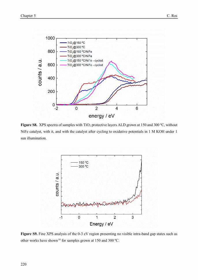
Chapter 5 C. Ros
220
Figure S8. XPS spectra of samples with TiO2 protective layers ALD grown at 150 and 300 ºC, without
NiFe catalyst, with it, and with the catalyst after cycling to oxidative potentials in 1 M KOH under 1
sun illumination.
Figure S9. Fine XPS analysis of the 0-3 eV region presenting no visible intra-band gap states such as
other works have shown10 for samples grown at 150 and 300 ºC.
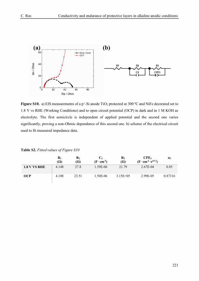
C. Ros Conductivity and endurance of protective layers in alkaline anodic conditions
221
Figure S10. a) EIS measurements of a p+-Si anode TiO2 protected at 300 ºC and NiFe decorated set to
1.8 V vs RHE (Working Conditions) and to open circuit potential (OCP) in dark and in 1 M KOH as
electrolyte. The first semicircle is independent of applied potential and the second one varies
significantly, proving a non-Ohmic dependence of this second one. b) scheme of the electrical circuit
used to fit measured impedance data.
Table S2. Fitted values of Figure S10
R1 (Ω)
R2 (Ω)
C2 (F· cm-2)
R3 (Ω)
CPE3 (F· cm-2 ·sα3-1)
α3
1.8 V VS RHE 4.148 27.8 1.59E-06 21.79 2.67E-04 0.85
OCP 4.108 23.51 1.50E-06 3.15E+05 2.99E-05 0.87316
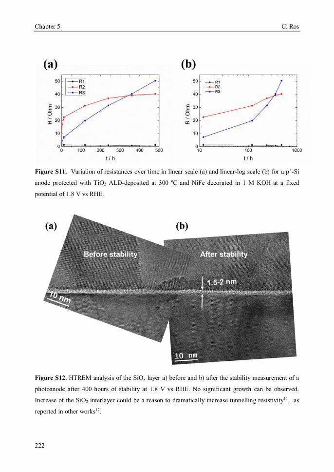
Chapter 5 C. Ros
222
Figure S11. Variation of resistances over time in linear scale (a) and linear-log scale (b) for a p+-Si
anode protected with TiO2 ALD-deposited at 300 ºC and NiFe decorated in 1 M KOH at a fixed
potential of 1.8 V vs RHE.
Figure S12. HTREM analysis of the SiOx layer a) before and b) after the stability measurement of a
photoanode after 400 hours of stability at 1.8 V vs RHE. No significant growth can be observed.
Increase of the SiO2 interlayer could be a reason to dramatically increase tunnelling resistivity11, as
reported in other works12.
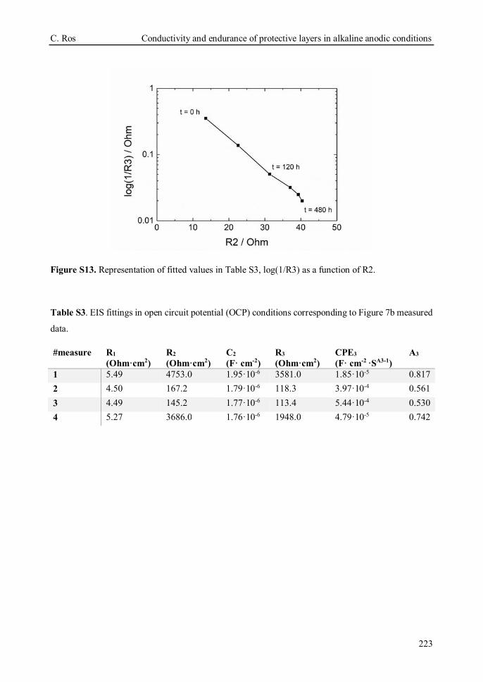
C. Ros Conductivity and endurance of protective layers in alkaline anodic conditions
223
Figure S13. Representation of fitted values in Table S3, log(1/R3) as a function of R2.
Table S3. EIS fittings in open circuit potential (OCP) conditions corresponding to Figure 7b measured
data.
#measure R1
(Ohm·cm2) R2
(Ohm·cm2) C2 (F· cm-2)
R3
(Ohm·cm2) CPE3 (F· cm-2 ·SA3-1)
A3
1 5.49 4753.0 1.95·10-6 3581.0 1.85·10-5 0.817 2 4.50 167.2 1.79·10-6 118.3 3.97·10-4 0.561 3 4.49 145.2 1.77·10-6 113.4 5.44·10-4 0.530 4 5.27 3686.0 1.76·10-6 1948.0 4.79·10-5 0.742
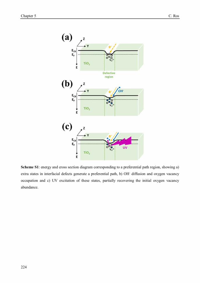
Chapter 5 C. Ros
224
Scheme S1: energy and cross section diagram corresponding to a preferential path region, showing a)
extra states in interfacial defects generate a preferential path, b) OH- diffusion and oxygen vacancy
occupation and c) UV excitation of these states, partially recovering the initial oxygen vacancy
abundance.
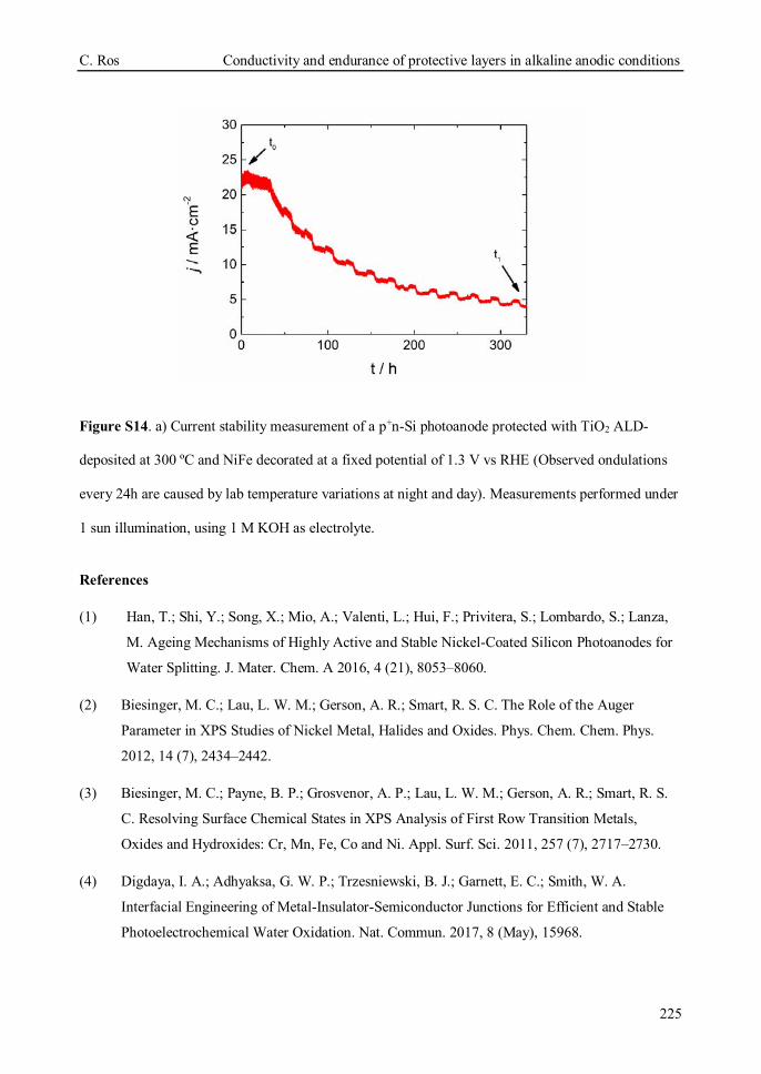
C. Ros Conductivity and endurance of protective layers in alkaline anodic conditions
225
Figure S14. a) Current stability measurement of a p+n-Si photoanode protected with TiO2 ALD-
deposited at 300 ºC and NiFe decorated at a fixed potential of 1.3 V vs RHE (Observed ondulations
every 24h are caused by lab temperature variations at night and day). Measurements performed under
1 sun illumination, using 1 M KOH as electrolyte.
References
(1) Han, T.; Shi, Y.; Song, X.; Mio, A.; Valenti, L.; Hui, F.; Privitera, S.; Lombardo, S.; Lanza,
M. Ageing Mechanisms of Highly Active and Stable Nickel-Coated Silicon Photoanodes for
Water Splitting. J. Mater. Chem. A 2016, 4 (21), 8053–8060.
(2) Biesinger, M. C.; Lau, L. W. M.; Gerson, A. R.; Smart, R. S. C. The Role of the Auger
Parameter in XPS Studies of Nickel Metal, Halides and Oxides. Phys. Chem. Chem. Phys.
2012, 14 (7), 2434–2442.
(3) Biesinger, M. C.; Payne, B. P.; Grosvenor, A. P.; Lau, L. W. M.; Gerson, A. R.; Smart, R. S.
C. Resolving Surface Chemical States in XPS Analysis of First Row Transition Metals,
Oxides and Hydroxides: Cr, Mn, Fe, Co and Ni. Appl. Surf. Sci. 2011, 257 (7), 2717–2730.
(4) Digdaya, I. A.; Adhyaksa, G. W. P.; Trzesniewski, B. J.; Garnett, E. C.; Smith, W. A.
Interfacial Engineering of Metal-Insulator-Semiconductor Junctions for Efficient and Stable
Photoelectrochemical Water Oxidation. Nat. Commun. 2017, 8 (May), 15968.
Chapter 5 C. Ros
226
(5) Mei, B.; Permyakova, A. a; Frydendal, R.; Bae, D.; Pedersen, T.; Malacrida, P.; Hansen, O.;
Stephens, I. E. L.; Vesborg, P. C. K.; Seger, B.; et al. Iron-Treated NiO as a Highly
Transparent p ‑ Type Protection Layer for E Ffi Cient Si-Based Photoanodes. J. Phys. Chem.
Lett. 2014, 5 (20), 3456–3461.
(6) Zhou, H.; Yu, F.; Zhu, Q.; Sun, J.; Qin, F.; Yu, L.; Bao, J.; Yu, Y. Water Splitting by
Electrolysis at High Current Density under 1.6 Volt. Energy Environ. Sci. 2018, No. 60 mL,
3–5.
(7) Lu, Z.; Xu, W.; Zhu, W.; Yang, Q.; Lei, X.; Liu, J.; Li, Y.; Sun, X.; Duan, X. Three-
Dimensional NiFe Layered Double Hydroxide Film for High-Efficiency Oxygen Evolution
Reaction. Chem. Commun. 2014, 50 (49), 6479–6482.
(8) Biesinger, M. C.; Lau, L. W. M.; Gerson, A. R.; Smart, R. S. C. Resolving Surface Chemical
States in XPS Analysis of First Row Transition Metals, Oxides and Hydroxides: Sc, Ti, V, Cu
and Zn. Appl. Surf. Sci. 2010, 257 (3), 887–898.
(9) Dette, C.; Hurst, M. R.; Deng, J.; Nellist, M. R.; Boettcher, S. W. Structural Evolution of
Metal (Oxy)Hydroxide Nanosheets during the Oxygen Evolution Reaction. 2018.
(10) Hu, S.; Shaner, M. R.; Beardslee, J. a; Lichterman, M.; Brunschwig, B. S.; Lewis, N. S.
Amorphous TiO₂ Coatings Stabilize Si, GaAs, and GaP Photoanodes for Efficient Water
Oxidation. Science 2014, 344 (6187), 1005–1009.
(11) Scheuermann, A. G.; Kemp, K. W.; Tang, K.; Lu, D. Q.; Satterthwaite, P. F.; Ito, T.; Chidsey,
C. E. D. D.; McIntyre, P. C.; Mc Intyre, P. C. Conductance and Capacitance of Bilayer
Protective Oxides for Silicon Water Splitting Anodes. Energy Environ. Sci. 2016, 9 (2), 1–26.
(12) Kiseok Oh, a Cristelle Meriadec, b Benedikt Lassalle-Kaiser, c Vincent Dorcet, a Bruno
Fabre, A.; Soraya Ababou-Girard, b Loic Joanny, d F. G. and G. L.; Oh, K.; Meriadec, C.;
Lassalle-Kaiser, B.; Dorcet, V.; Fabre, B.; Ababou-Girard, S.; Joanny, L.; Gouttefangeas, F.;
et al. Elucidating the Performance and Unexpected Stability of Partially Coated Water-
Splitting Silicon Photoanodes. Energy Environ. Sci. 2018, 0–11.

C. Ros Conductivity and endurance of protective layers in alkaline anodic conditions
227

Chapter 5 C. Ros
228

C. Ros Conductivity and endurance of protective layers in alkaline anodic conditions
229
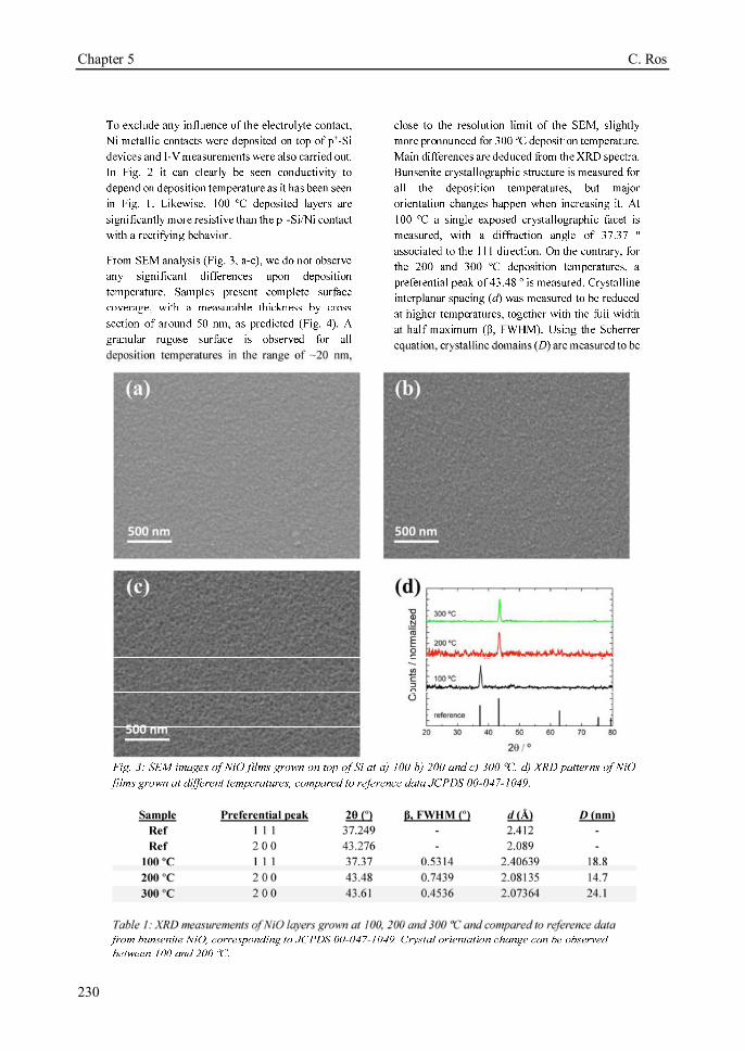
Chapter 5 C. Ros
230
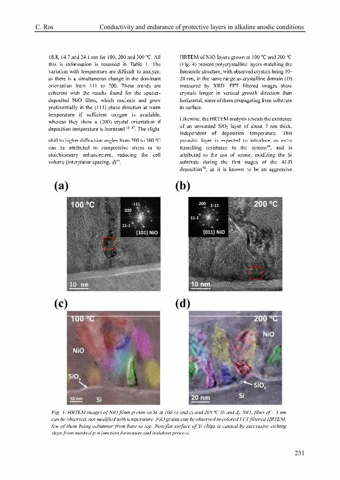
C. Ros Conductivity and endurance of protective layers in alkaline anodic conditions
231
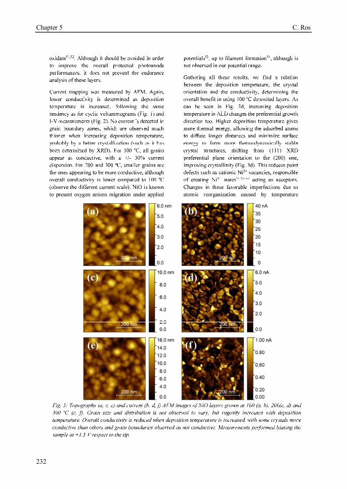
Chapter 5 C. Ros
232
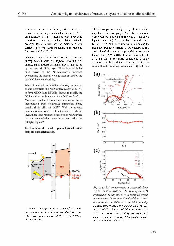
C. Ros Conductivity and endurance of protective layers in alkaline anodic conditions
233

Chapter 5 C. Ros
234

C. Ros Conductivity and endurance of protective layers in alkaline anodic conditions
235

Chapter 5 C. Ros
236
C. Ros Conductivity and endurance of protective layers in alkaline anodic conditions
237
Chapter 5 C. Ros
238
C. Ros Conductivity and endurance of protective layers in alkaline anodic conditions
239

Chapter 5 C. Ros
240

C. Ros Conductivity and endurance of protective layers in alkaline anodic conditions
241
About degradation and regeneration mechanisms of NiO protective layers deposited by ALD on photoanodes Carles Rosa,*, Teresa Andreua,b,*, Jordi Arbiolc,d, Joan R. Morantea,b
a Catalonia Institute for Energy Research (IREC). Jardins de les Dones de Negre 1, 08930 Sant Adrià del Besòs, Barcelona, Spain b Universitat de Barcelona (UB), Martí i Franquès, 1, 08028 Barcelona, Spain cCatalan Institute of Nanoscience and Nanotechnology (ICN2), CSIC and The Barcelona Institute of Science and Technology (BIST), Campus UAB, Bellaterra, 08193 Barcelona, Spain dICREA, Pg. Lluís Companys 23, 08010 Barcelona, Spain
Supporting Information
Fig. S. 1: p+n-Si photoanode, where a 0.5 cm2 active area (darker region) was lithographically defined by SiO2 passivation on a silicon n-type wafer (0.1-0.5 ohm.cm resistivity), ALD-protected and further Ag paint soldered to a Cu wire and isolated with thermoplastic.

Chapter 5 C. Ros
242
Fig S. 2: Zoom in the 200 and 300 ºC region of cyclic voltammograms presented in Fig. 1, in 1 M KOH of a) p+-Si anodes protected with ALD deposited NiO layers at 100 ºC (red) 200 ºC (blue) and 300 ºC (green), cycles 1, 10, 50 and 100 from darker to clearer color.
Fig S. 3: transmittance measurements of NiO layers grown at 100 (black), 200 (red) and 300 ºC (blue) on top of glass substrates.
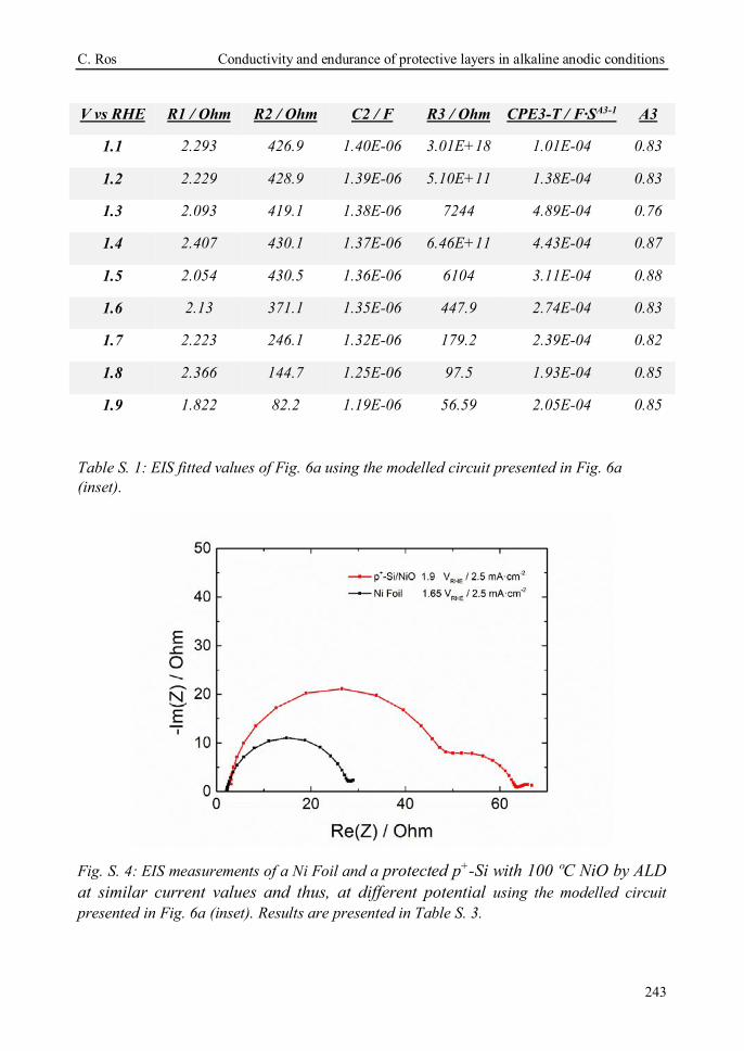
C. Ros Conductivity and endurance of protective layers in alkaline anodic conditions
243
V vs RHE R1 / Ohm R2 / Ohm C2 / F R3 / Ohm CPE3-T / F·SA3-1 A3
1.1 2.293 426.9 1.40E-06 3.01E+18 1.01E-04 0.83
1.2 2.229 428.9 1.39E-06 5.10E+11 1.38E-04 0.83
1.3 2.093 419.1 1.38E-06 7244 4.89E-04 0.76
1.4 2.407 430.1 1.37E-06 6.46E+11 4.43E-04 0.87
1.5 2.054 430.5 1.36E-06 6104 3.11E-04 0.88
1.6 2.13 371.1 1.35E-06 447.9 2.74E-04 0.83
1.7 2.223 246.1 1.32E-06 179.2 2.39E-04 0.82
1.8 2.366 144.7 1.25E-06 97.5 1.93E-04 0.85
1.9 1.822 82.2 1.19E-06 56.59 2.05E-04 0.85
Table S. 1: EIS fitted values of Fig. 6a using the modelled circuit presented in Fig. 6a (inset).
Fig. S. 4: EIS measurements of a Ni Foil and a protected p+-Si with 100 ºC NiO by ALD at similar current values and thus, at different potential using the modelled circuit presented in Fig. 6a (inset). Results are presented in Table S. 3.
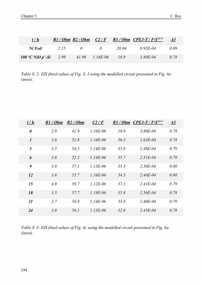
Chapter 5 C. Ros
244
t / h R1 / Ohm R2 / Ohm C2 / F R3 / Ohm CPE3-T / F·SA3-1 A3
Ni Foil 2.15 0 0 26.04 8.92E-04 0.89
100 ºC NiO p+-Si 2.99 41.96 1.16E-06 18.9 3.80E-04 0.78
Table S. 2: EIS fitted values of Fig. S. 3 using the modelled circuit presented in Fig. 6a (inset).
t / h R1 / Ohm R2 / Ohm C2 / F R3 / Ohm CPE3-T / F·SA3-1 A3
0 2.9 41.9 1.16E-06 18.9 3.80E-04 0.78
1 3.6 52.8 1.16E-06 36.3 2.63E-04 0.78
3 3.5 54.3 1.14E-06 35.8 2.48E-04 0.79
6 3.6 55.2 1.14E-06 35.7 2.51E-04 0.79
9 3.8 57.1 1.13E-06 35.3 2.36E-04 0.80
12 3.6 55.7 1.16E-06 34.3 2.46E-04 0.80
15 4.0 59.7 1.12E-06 37.1 2.41E-04 0.79
18 3.5 57.7 1.18E-06 35.8 2.56E-04 0.78
21 3.7 56.8 1.14E-06 33.8 2.40E-04 0.79
24 3.8 56.1 1.13E-06 32.8 2.45E-04 0.79
Table S. 3: EIS fitted values of Fig. 6c using the modelled circuit presented in Fig. 6a (inset).
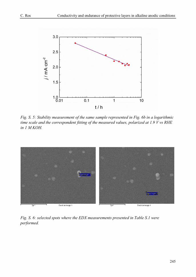
C. Ros Conductivity and endurance of protective layers in alkaline anodic conditions
245
Fig. S. 5: Stability measurement of the same sample represented in Fig. 6b in a logarithmic time scale and the correspondent fitting of the measured values, polarized at 1.9 V vs RHE in 1 M KOH.
Fig. S. 6: selected spots where the EDX measurements presented in Table S.1 were performed.

Chapter 5 C. Ros
246
Spectrum 2 Spectrum 3 Element Weight% Atomic%
C K 15.84 28.17
O K 15.34 20.49
F K 7.06 7.94
Al K 0.29 0.23
Si K 52.31 39.79
S K 0.14 0.10
Ni K 9.01 3.28
Totals 100.00
Element Weight% Atomic%
C K 30.38 48.55
O K 8.57 10.28
F K 1.73 1.75
Al K 0.00 0.00
Si K 56.13 38.36
S K 0.08 0.05
Ni K 3.12 1.02
Totals 100.00
Table S. 4: EDX quantifications of spots selected in Fig. S. 4, presenting significant extra Ni and O where bumps are visible by SEM.
Fig. S. 7: SEM images of NiO layers grown on top of Si at deposition temperatures of 200 ºC (left) and 300 ºC (right) after 100 cycles between 1.1 and 2 V vs RHE in 1 M KOH electrolyte in dark conditions. No morphology changes can be seen.

C. Ros Conductivity and endurance of protective layers in alkaline anodic conditions
247
Fig. S. 8: a) Stability measurement of a FTO covered with 50 nm of NiO at 100 ºC and under stability for 18h at 1.9 V vs RHE in 1 M KOH. b) In-situ transmittance measurement of the FTO and NiO layers showing no apparent variation after 18 h stability and ~40% current decay.

Chapter 5 C. Ros
248
Fig. S. 9: a) SEM top view image of the n+p-Si photoanode NiO protected at 100 ºC presenting very few etched regions. Zoom in two of the etching regions, where b) a few tens of nanometers hole can be seen and c) a particle is present, both probable fabrication defects of the NiO layer allowing KOH to etch the silicon beneath.

Conclusions and future work

Conclusions and future work C. Ros
250

C. Ros Conclusions and future work
251
The main objective of this thesis has been to study efficient and stable front illuminated photoelectrodes for photoelectrochemical water splitting, with special attention on cost-effective materials. Focus has been put on characterizing materials performance and stability for the two considered configurations, metal oxide based photoelectrodes and protective layers on unstable short band gap photoabsorbers. The protection of silicon and chalcogenide based photoelectrodes resulted in significantly superior productivities than studied metal oxide photoanodes, thus centering most of our efforts. For better understanding of protective layers characteristics, conductivity and degradation analyses were also performed at the nanoscale level.
In the first part of this thesis, titanium dioxide (TiO2) based photoanodes are studied, giving to the following conclusions:
Performance increases with thicker and denser nanorods film, caused by higher active area, which is obtained with increasing precursor concentration during hydrothermal growth. There is a maximum precursor concentration of 45 mM, over which TiO2 film detaches from substrate.
Substrate microstructuration further enhances productivity by increased direct and scattered light absorption and electrode’s area.
A thermal treatment in a reductive H2 atmosphere increases the n-type semiconductor level. This way, the seminconductor-liquid junction (SCLJ) was optimized to maximize nanorods potential drop, enhancing charge separation and transport and thus, increasing photoanodes performance.
By incident photon-to-current efficiency (IPCE) it was corroborated that the performance increase after the H2 treatment was caused by a better charge extraction in the UV range rather than absorption of visible light by treatment-created states inside the band gap.
Collaterally, it was observed remarkable different spectral response of TiO2 photoanodes with and without a light bias, increasing effective available charge carriers and filling trap states active under low monochromatic illumination intensities. This finding helps for more reliable future IPCE measurements.
Up to 1.2 mA·cm-2 photocurrent at 1.23 V vs RHE was obtained by these morphological, microscopical and electronic modifications, which corresponds to about a 65% of its theoretical maximum photocurent.
A 3.0 eV semiconductor is limited to absorb a ~5% of the solar spectra, the UV part. Even with the triple strategy followed to enhance TiO2 photoanodes performance, results are limited. More complex configurations, involving more efficient and short band gap semiconductors, must be implemented to obtain higher productivities.

Conclusions and future work C. Ros
252
In the second part of this thesis, buried short band gap semiconductor junctions, already known from photovoltaic technology, are implemented for photocathodic hydrogen evolution in acidic electrolytes, to favor the hydrogen evolution reaction (HER). Atomic layer deposited (ALD) TiO2 protective layers are used to inhibit corrosion of unstable photoabsorber candidates, first optimized on silicon. Platinum is used as a model HER catalyst since its overpotential is close to 0, thus studying catalysts was not the scope of this work. The main conclusions of this section are:
The deposition temperature is found to be a key parameter for stability and conductivity, directly related to crystallization, starting between 100 and 200 ºC. Films deposited at 300 ºC presented high conductivity, transparency, and polycrystalline morphology, allowing over 20 mA·cm-2 at 0.4 V vs RHE stable for over 300 h in 0.5 M H2SO4.
Crystalline grains are responsible for electron conduction, revealed by conductive atomic force microscopy (c-AFM), unlike amorphous zones where no current can be measured.
Amorphous TiO2 regions present in mixed amorphous-crystalline films are found to dissolve in cathodic conditions and acidic electrolytes, exposing the substrate to the electrolyte.
5 nm Ti intermediate layer between Si and TiO2 is found to help in ALD-TiO2 crystalline nucleation and to prevent native SiO2 detrimental formation at the Si/TiO2 interface.
These protective layers are also deposited on chalcogenide photoabsorbers, from which it were depicted the following conclusions:
Copper-indium-gallium-selenide (CIGS) photoabsorbers on flexible stainless steel substrates can be converted in efficient PEC devices with over 40 mA·cm-2 photocurrents and 450 mV photovoltages.
The use of the complete multilayer stack (n-CdS/i-ZnO/AZO) used for CIGS solar cells is needed for efficient charge separation and electron transport to the hydrogen evolution reaction.
Devices fabricated on flexible substrates result in detrimental cracks in the protective layer, allowing acid to corrode the photocathode.
Indium and gallium can be substituted by zinc and tin, earth abundant elements. These kesterite-structured copper-zinc-tin-sulfide/selenide (CZTS/Se) based solar cells can also be transformed into photocathodes by ALD-TiO2 protection and Pt catalyst decoration.
By modifying the sulfur/selenium ratio, the optical band gap can be tuned (1.0-1.5 eV), together with the final cathode photovoltage. This characteristic is highly interesting to form tandem PEC devices.
C. Ros Conclusions and future work
253
The kesterite-based cells electronic structure and p-n junction, defined by optimized distribution of copper vacancies and Cu/Zn antisite defects, is highly sensible to thermal post treatments, limiting ALD deposition temperatures to 200 ºC. ALD is especially interesting deposition technique due forming crystalline films at such low deposition temperature, given by intermediate species mobility and slow deposition. Pure-sulfide kesterites suffer from partial band gap decrease even at 200 ºC.
ALD has demonstrated to protect kesterite-based solar cells on glass substrates giving over 25 mA·cm-2 stable photocurrent for more than 1 h in acidic electrolyte.
Thanks to the possibility to measure solar cells with and without the protective layer, the electrical resistance and changes in its performance can be measured and the catalytic response calculated, allowing us to describe a series circuit model including the role of each component.
In the last part of the thesis, TiO2 and NiO protective layers are studied in anodic conditions and alkaline electrolytes (favorable for the oxygen evolution reaction, OER). Silicon (with buried homojunctions) is used as reference photoabsorber as it is unaffected by the range of temperatures used for ALD deposition (100-300 ºC).
In the first work, TiO2 layers are deposited, followed by 5 nm NiFe as catalyst (which is hydroxylated to Ni(Fe)OOH in contact with alkaline electrolytes, one of the best catalyst for oxygen evolution). The main findings are:
Conductivity is enabled when crystallinity is present. This is demonstrated by depositing completely amorphous, mixed amorphous-crystalline and completely crystalline TiO2 films. Preferential paths in crystalline grains are observed to be the responsible of conductivity in TiO2 by micro-Raman and c-AFM measurements. This points towards electron injection from the catalyst to the conduction band of TiO2 and a tunneling recombining contact constituted by the p+-Si/2.5 nm SiO2/TiO2 interface.
HRTEM analysis presents polycrystallinity inside the observed grains, and preferential conductivity paths are attributed to grain boundaries and defects within the crystalline structure.
TiO2-based protective films present logarithmic current decay under continuous polarization over 480 h stability tests. Electrochemical impedance spectroscopy (EIS) corroborates an increase of the capacity attributed to depletions inside the TiO2 film. OH- ions are considered to diffuse into TiO2 under anodic conditions and alter semiconductor’s conduction paths conductivity
UV superimposed illumination partially recovers conductivity of the film, considered a persistent photoconductivity effect on TiO2 due to modifications on states occupancy.
Conclusions and future work C. Ros
254
Alternatively, a one-step ALD deposition of NiO films at 100, 200 and 300 ºC creates protected photoanodes with optimal catalytic surface in contact with alkaline electrolytes, where:
The most conductive layers were formed at low deposition temperature of 100 ºC, attributed to less stoichiometric films, with more Ni2+ vacancies, responsible of the p-type semiconductor conductivity. Temperature increase was found to result in a crystalline growth direction variation, simultaneous to conductivity reduction.
Current density decays following a logarithmic time dependency, pointing at the formation of a self-passivation layer. This is attributed to the interaction of the NiO layer and the alkaline electrolyte under anodic working conditions, forming of higher nickel oxidation states at the electrode/electrolyte interface, resulting in an OER overpotential increase.
Nevertheless, the application of periodic cycling ranging from anodic to cathodic voltage conditions corroborates the existence of a recovery procedure based the cathodic scans promoting the reduced forms at the surface of the NiO layer.
Applying this methodology under 3 hours cycling periodicity, over 1000 h stability measurements were possible with over 11 mA·cm-2 photocurrents, an 85% of the initial photocurrent.
In conclusion, the works included in this thesis are significant contributions to the study of fundamental properties of materials and more specifically, stable and efficient photoelectrodes for photoelectrochemical water splitting and their degradation mechanisms. A broad study is performed on ALD deposition of metal oxides and the relationship of these protective thin films with buried semiconductor p-n junctions. The results included have allowed a great improvement of IREC’s both maximum productivities and knowledge on short band gap semiconductors and protective layers for harsh chemical environments. In the end, the presented results contribute in the multidisciplinary field of photoelectrochemistry, and should bring stable and efficient photoelectrodes a step closer to commercial application.
Future work:
Nevertheless, despite all the knowledge gained during recent years, efficient and long-stable photoelectrochemical devices have still some challenges to overcome for their large-scale implementation. Silicon presents optimal characteristics for absorbing the red part of visible spectra in tandem structures, but efficient ~1.7 eV band gap earth abundant candidates (absorbing only the blue and green part of the visible spectra) must be found. In this direction, chalcogenide-based photoelectrodes have been demonstrated especially interesting due to the possibility of adapting their band gap by varying the chalcogenide composition. Simplifying the multilayer structure for chalcogenide based PEC devices, i.e. with chemically stable metal oxides acting directly as TCO, might increase their stability in harsh electrolytes and reduce

C. Ros Conclusions and future work
255
fabrication costs. The substitution of high vacuum deposition and time-consuming techniques would reduce fabrication costs if pinhole-free layers can be assured. Optimizing the protective layer thickness as antireflective layer will surely help in increasing photoelectrodes productivity. Very long-term stability measurements, in intermittent day/night operation will be necessary to prove protective layers strategy viable in years-lasting devices.

Conclusions and future work C. Ros
256

Annex

Annex C. Ros
258
C. Ros Annex
259
In the annex chapter of this thesis three works are included, which are considered better suited outside the main part of the thesis, since they are the result of collaborative work coming from the knowledge gained through the development of the PhD work. In the first article, related to hematite photoanodes, the contribution of the thesis author has been minor, related to the TiO2-ALD deposition prior to anneal treatment, to form the Fe2TiO5 superficial layer helping to control surface states and electronic interface coupling. In the second one, the n+p-Si/Ti/TiO2 photocathodes described in Chapter 3 are implemented in another energy storage technology, vanadium redox flow batteries. Due to the evident divergence with water splitting focus of this thesis it has been considered better suited in the annex. The third work included in this chapter is a patent published in collaboration with an industry, where interdigitated back contact (IBC) solar cells are implemented for PEC water splitting with different protective strategies, one of them ALD-deposited TiO2 films. Due to intellectual property reasons, only the patented content of the work related to this study is reprinted here.
A.1. Enhanced photoelectrochemical water splitting of hematite multilayer nanowire photoanodes by tuning the surface state via bottom-up interfacial engineering
In the first article included in this chapter a sequential study on detrimental interfacial electron-hole recombination of hematite based photoanodes is performed. Multilayered nanowires ITO/Fe2O3/Fe2TiO5/FeNiOOH are fabricated, with optimized deposition and post-treatments, to facilitate charge transport from the electrochemical reaction into the back contact.
Fe2O3 nanowires were grown by a hydrothermal process on and different-thickness indium-doped tin oxide (ITO) covered or no-ITO FTO substrates. Further post-treatments and quenching in air with none or few nanometers ALD-TiO2 on top allowed forming the Fe2TiO5 superficial layer. FeNiOOH nanodots are later photoelectrodeposited on top. The characterization of the photoelectrodes with and without extra interfaces helped elucidating the role of each one.
The systematic electrochemical measurements, and extensive HRTEM and STEM-EELS analysis permitted defining the elemental distribution inside the nanostructures and modeling the electronic interface coupling (Figure A.1a). Epitaxial growth and optimal control of thermal treatments help improve the ITO/Fe2O3 interface, with Sn diffusing as doping in Fe2O3 structure, reducing back contact recombination. ALD-TiO2 followed by thermal post-treatments formed Fe2TiO5, with favorable energetics for charge separation and Ti atoms passivating detrimental sites in a core-shell nanowire structure. Together with FeNiOOH nanodots increasing electrochemically active sites for OER, electron-hole recombination rates are reduced.
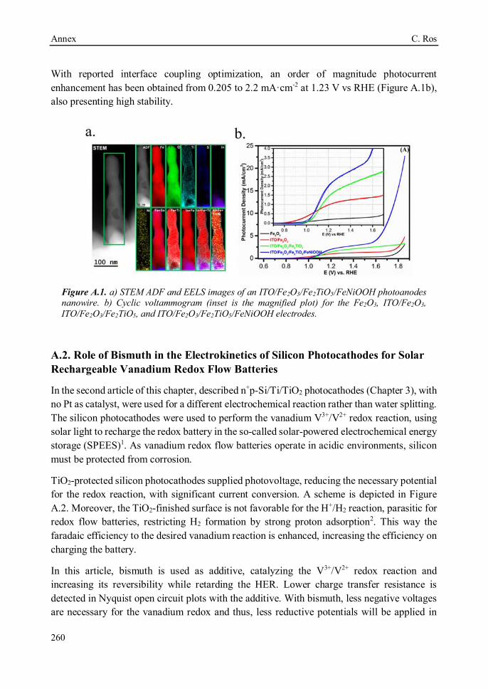
Annex C. Ros
260
With reported interface coupling optimization, an order of magnitude photocurrent enhancement has been obtained from 0.205 to 2.2 mA·cm-2 at 1.23 V vs RHE (Figure A.1b), also presenting high stability.
Figure A.1. a) STEM ADF and EELS images of an ITO/Fe2O3/Fe2TiO5/FeNiOOH photoanodes nanowire. b) Cyclic voltammogram (inset is the magnified plot) for the Fe2O3, ITO/Fe2O3, ITO/Fe2O3/Fe2TiO5, and ITO/Fe2O3/Fe2TiO5/FeNiOOH electrodes.
A.2. Role of Bismuth in the Electrokinetics of Silicon Photocathodes for Solar Rechargeable Vanadium Redox Flow Batteries
In the second article of this chapter, described n+p-Si/Ti/TiO2 photocathodes (Chapter 3), with no Pt as catalyst, were used for a different electrochemical reaction rather than water splitting. The silicon photocathodes were used to perform the vanadium V3+/V2+ redox reaction, using solar light to recharge the redox battery in the so-called solar-powered electrochemical energy storage (SPEES)1. As vanadium redox flow batteries operate in acidic environments, silicon must be protected from corrosion.
TiO2-protected silicon photocathodes supplied photovoltage, reducing the necessary potential for the redox reaction, with significant current conversion. A scheme is depicted in Figure A.2. Moreover, the TiO2-finished surface is not favorable for the H+/H2 reaction, parasitic for redox flow batteries, restricting H2 formation by strong proton adsorption2. This way the faradaic efficiency to the desired vanadium reaction is enhanced, increasing the efficiency on charging the battery.
In this article, bismuth is used as additive, catalyzing the V3+/V2+ redox reaction and increasing its reversibility while retarding the HER. Lower charge transfer resistance is detected in Nyquist open circuit plots with the additive. With bismuth, less negative voltages are necessary for the vanadium redox and thus, less reductive potentials will be applied in
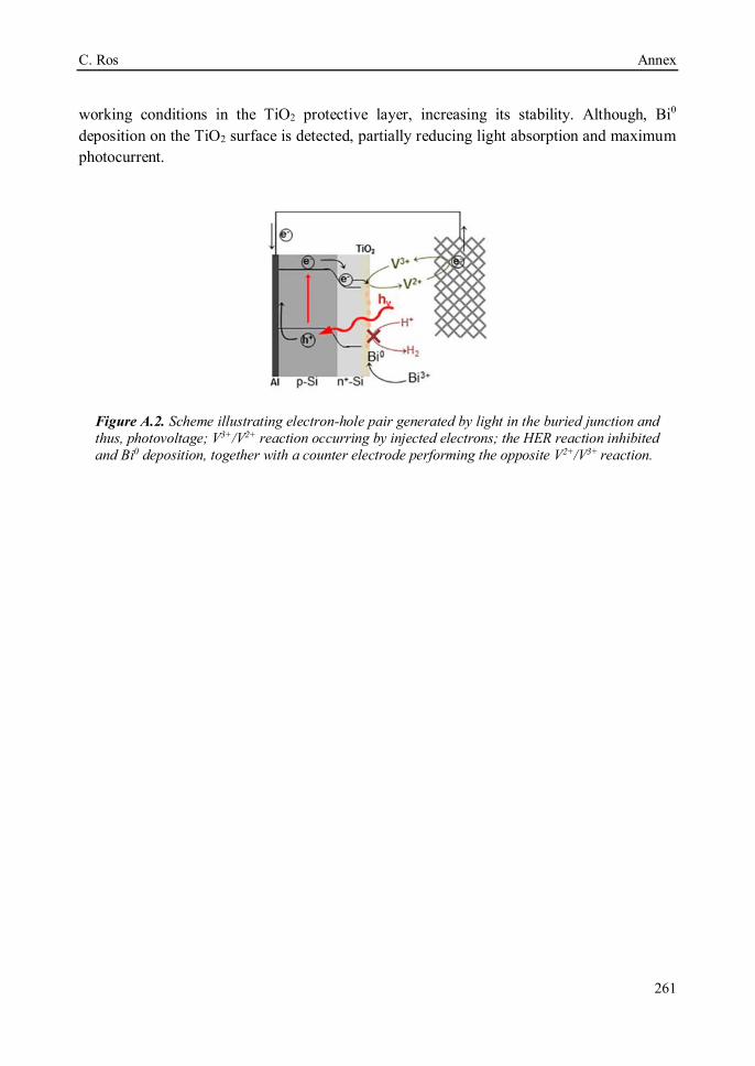
C. Ros Annex
261
working conditions in the TiO2 protective layer, increasing its stability. Although, Bi0 deposition on the TiO2 surface is detected, partially reducing light absorption and maximum photocurrent.
Figure A.2. Scheme illustrating electron-hole pair generated by light in the buried junction and thus, photovoltage; V3+/V2+ reaction occurring by injected electrons; the HER reaction inhibited and Bi0 deposition, together with a counter electrode performing the opposite V2+/V3+ reaction.
Annex C. Ros
262
A.3 Substrate-electrode (SE) interface illuminated photoelectrodes and photoelectrochemical cells
In the third work included in this annex chapter (patent WO/2017/109108, first page reprinted in page 327), interdigitated back contact (IBC) solar cells are implemented for PEC water splitting. Selectively, a resin layer isolates one of the back contacts (collector) from performing any reaction with the electrolyte. The non-isolated one (emitter) charges are conducted through a passivation layer and reaching electrocatalyst, performing the desired reaction. In one of the strategies presented in this patent, ALD-grown TiO2 layers as reported in Chapter 3 are used as protective, conductive layers together with platinum as HER catalyst. In this strategy, the transparency of these layers is not an issue as IBC solar cells are illuminated from the substrate-electrode (SE) interface side. The possibility of this scheme is demonstrated, together with high current densities equivalent to the photovoltaic ones and over one hour stability.
Bibliography
(1) Yu, M.; McCulloch, W. D.; Huang, Z.; Trang, B. B.; Lu, J.; Amine, K.; Wu, Y. Solar-Powered Electrochemical Energy Storage: An Alternative to Solar Fuels. J. Mater. Chem. A 2016, 4 (8), 2766–2782.
(2) Vázquez-Galván, J.; Flox, C.; Fàbrega, C.; Ventosa, E.; Parra, A.; Andreu, T.; Morante, J. R. Hydrogen-Treated Rutile TiO2 Shell in Graphite-Core Structure as a Negative Electrode for High-Performance Vanadium Redox Flow Batteries. ChemSusChem 2017, 10 (9), 2089–2098.

C. Ros Annex
263

Annex C. Ros
264

C. Ros Annex
265

Annex C. Ros
266

C. Ros Annex
267

Annex C. Ros
268
C. Ros Annex
269
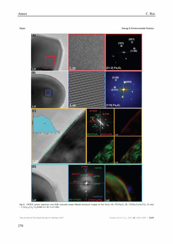
Annex C. Ros
270
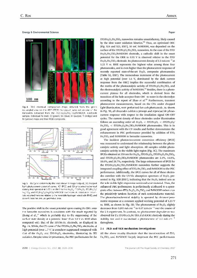
C. Ros Annex
271
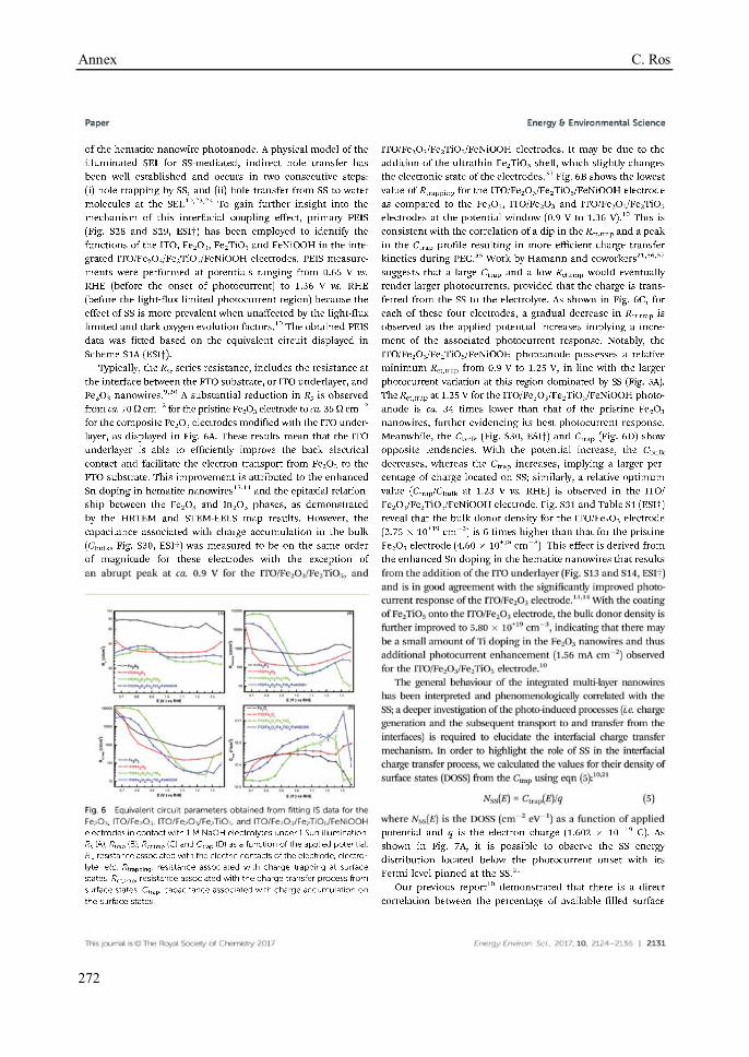
Annex C. Ros
272
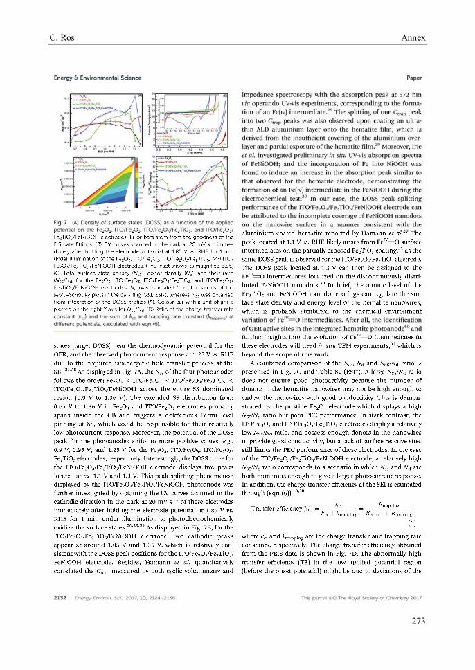
C. Ros Annex
273
Annex C. Ros
274
C. Ros Annex
275
Annex C. Ros
276
C. Ros Annex
277
Annex C. Ros
278

C. Ros Annex
279
Annex C. Ros
280
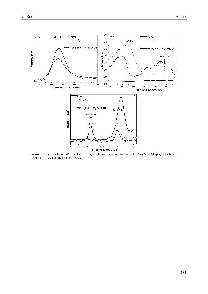
C. Ros Annex
281
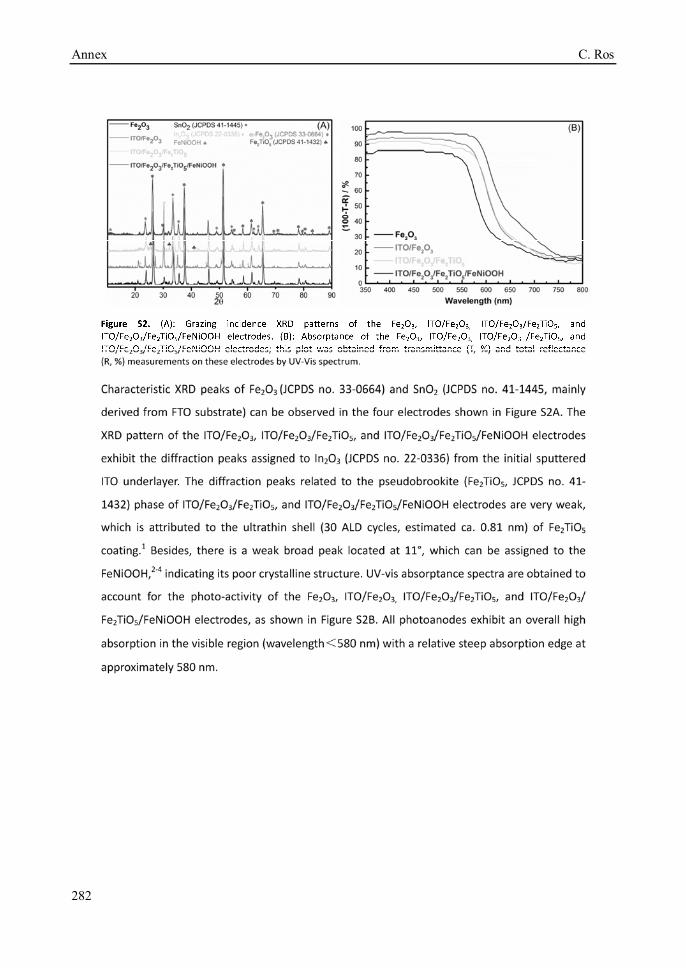
Annex C. Ros
282
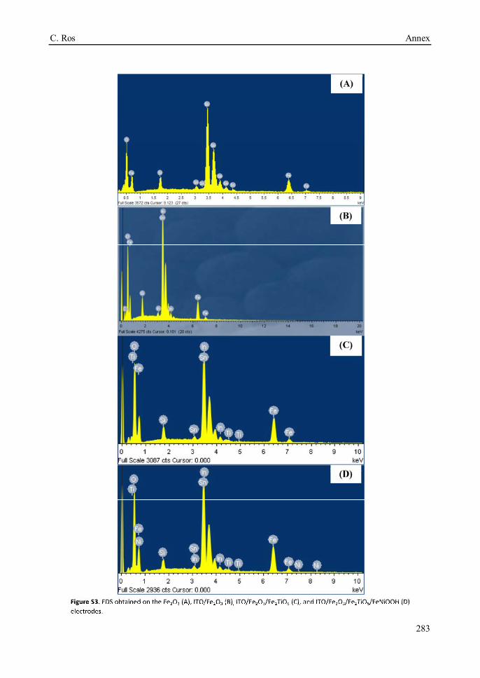
C. Ros Annex
283

Annex C. Ros
284
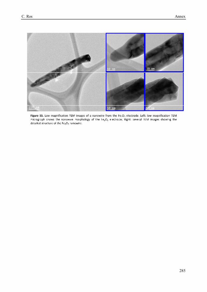
C. Ros Annex
285
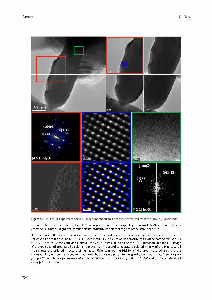
Annex C. Ros
286
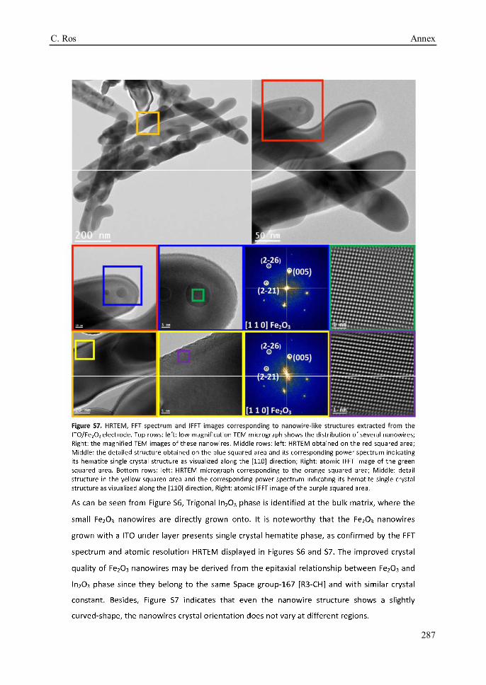
C. Ros Annex
287
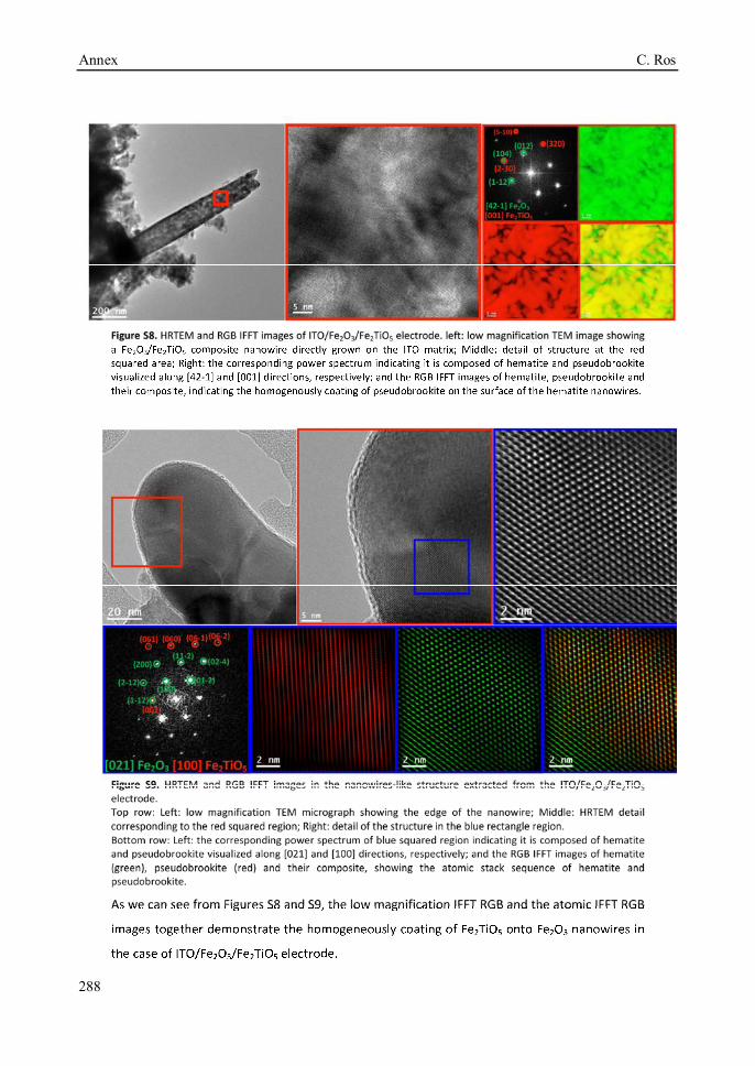
Annex C. Ros
288
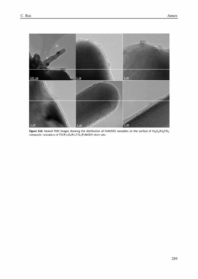
C. Ros Annex
289
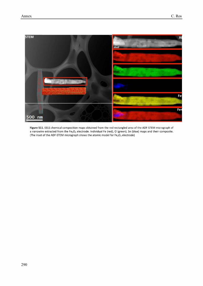
Annex C. Ros
290
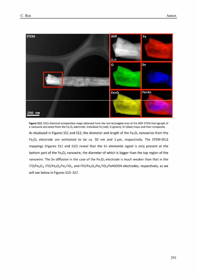
C. Ros Annex
291
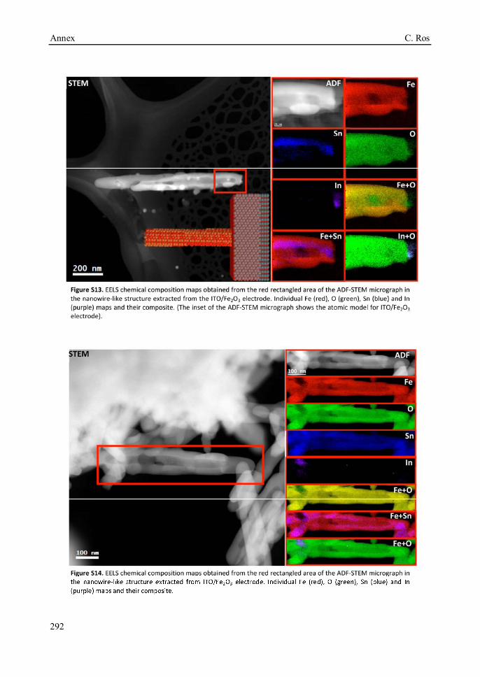
Annex C. Ros
292
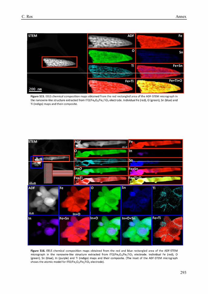
C. Ros Annex
293
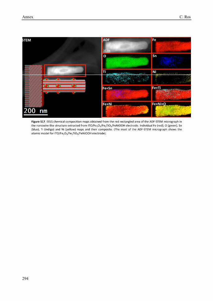
Annex C. Ros
294

C. Ros Annex
295
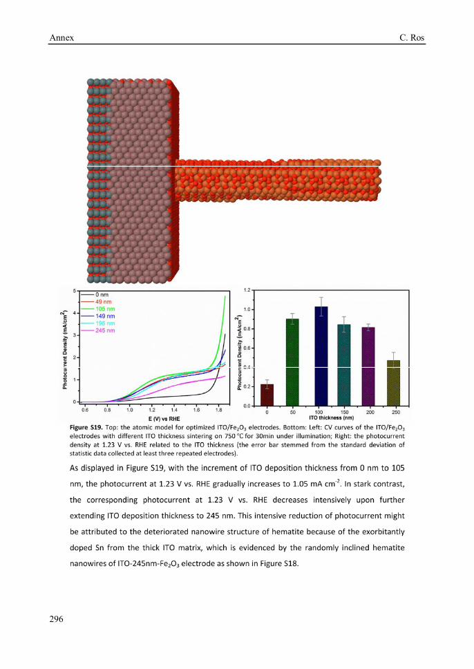
Annex C. Ros
296

C. Ros Annex
297

Annex C. Ros
298
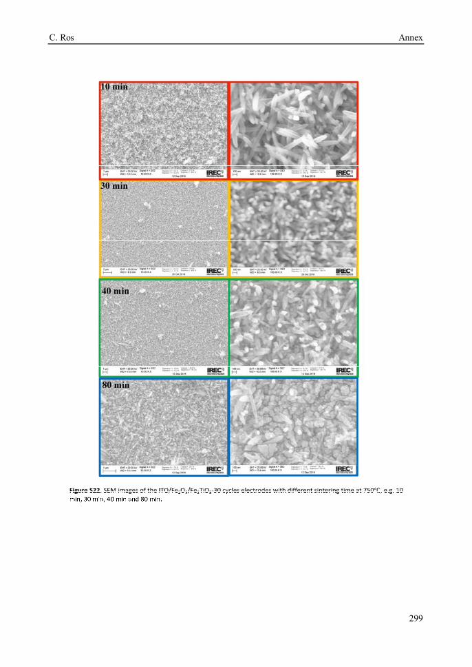
C. Ros Annex
299
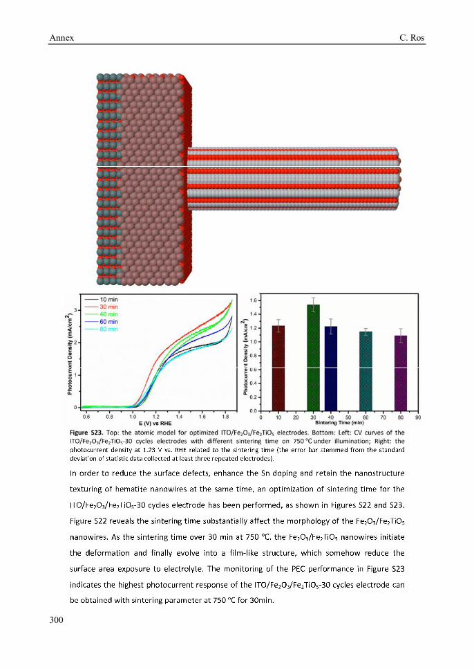
Annex C. Ros
300

C. Ros Annex
301

Annex C. Ros
302
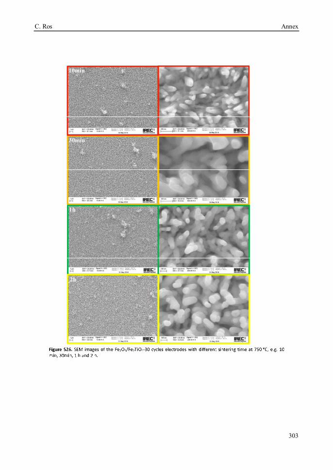
C. Ros Annex
303

Annex C. Ros
304
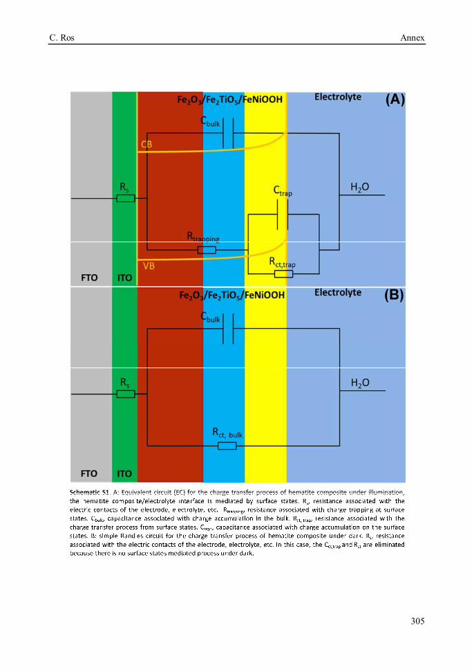
C. Ros Annex
305

Annex C. Ros
306
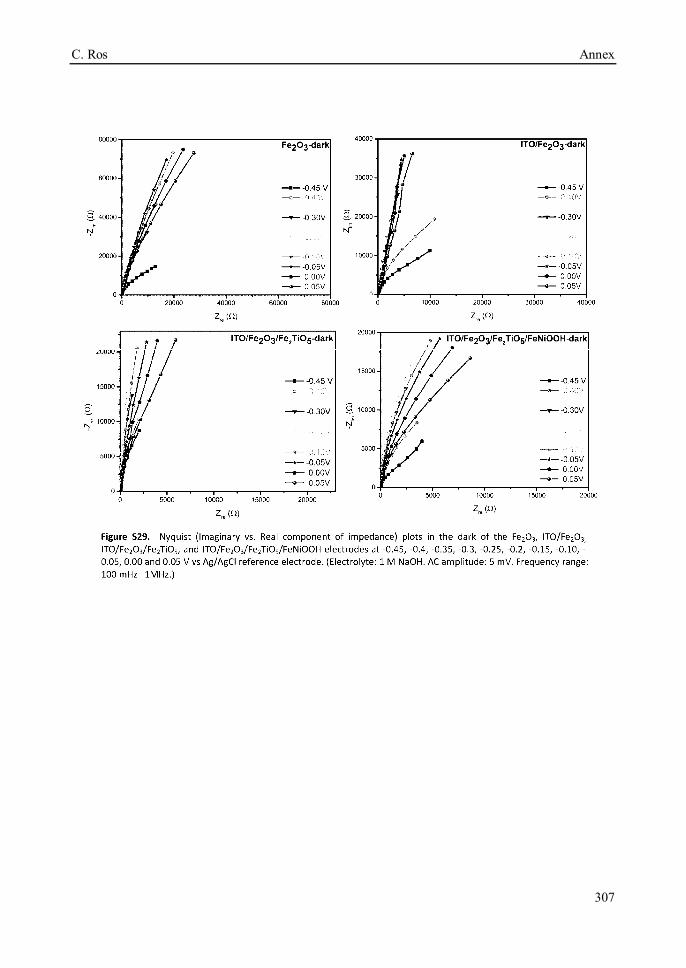
C. Ros Annex
307
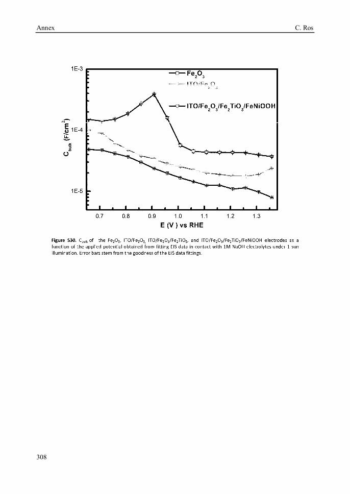
Annex C. Ros
308

C. Ros Annex
309
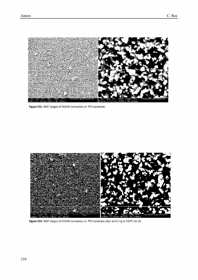
Annex C. Ros
310
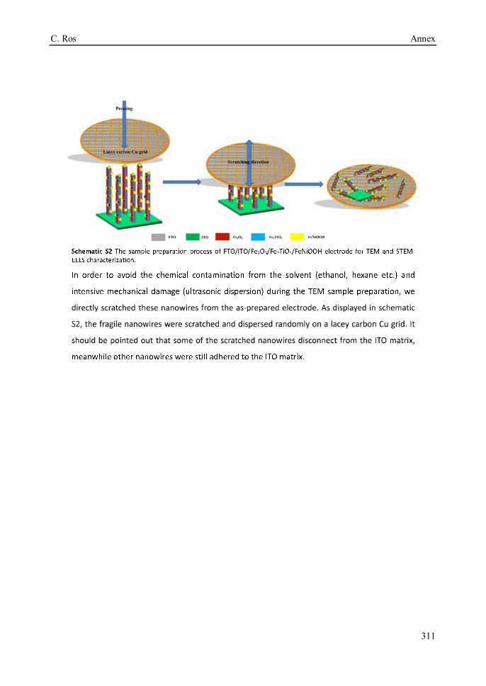
C. Ros Annex
311
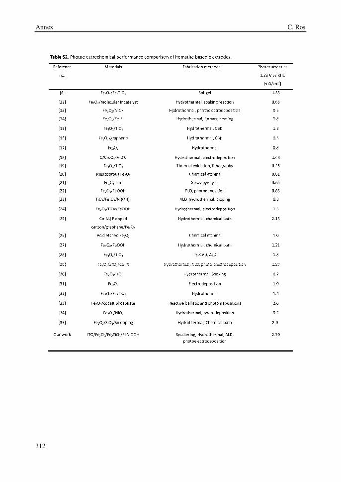
Annex C. Ros
312
C. Ros Annex
313

Annex C. Ros
314

C. Ros Annex
315
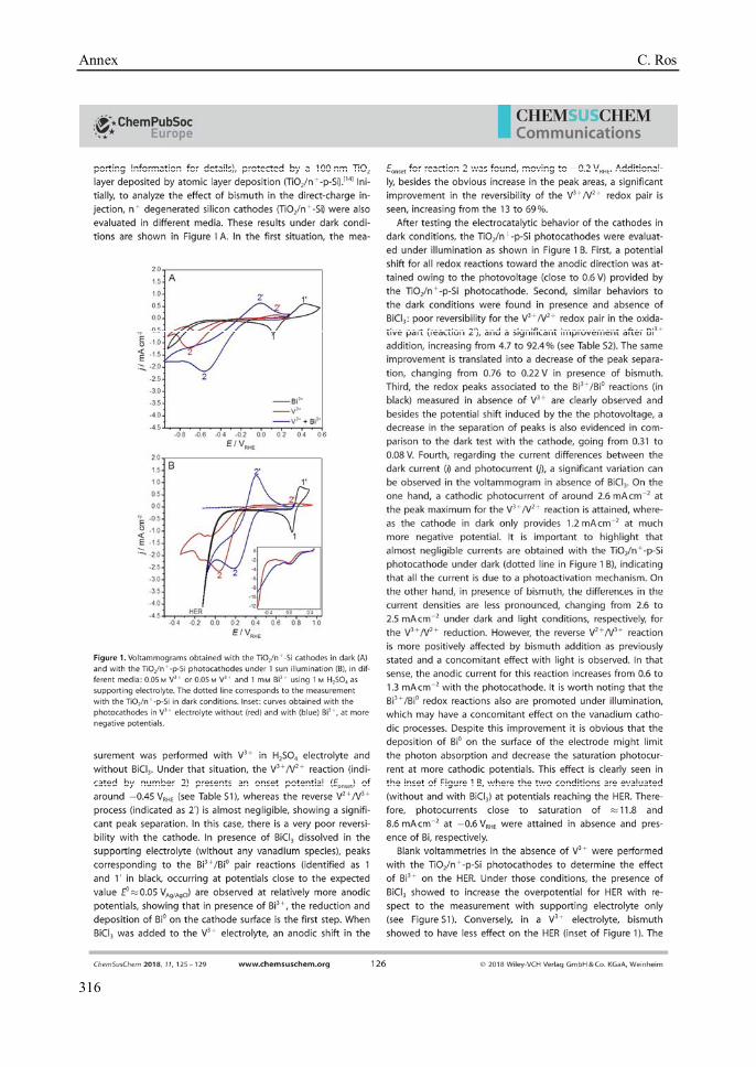
Annex C. Ros
316
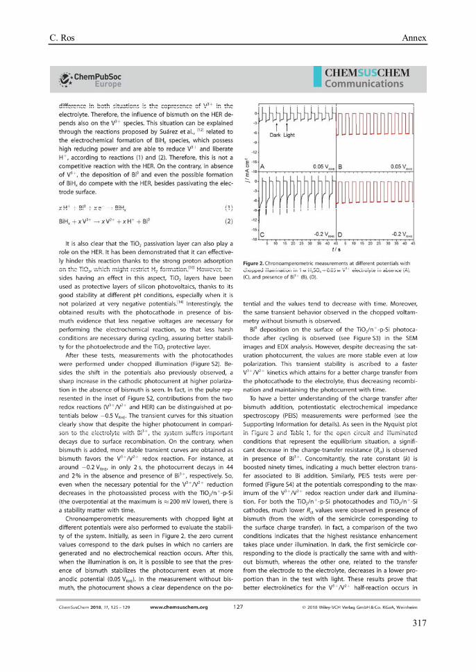
C. Ros Annex
317
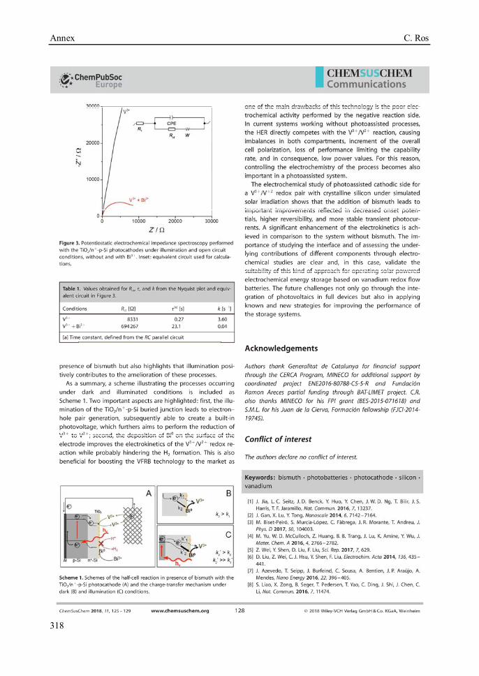
Annex C. Ros
318

C. Ros Annex
319
Annex C. Ros
320

C. Ros Annex
321

Annex C. Ros
322

C. Ros Annex
323
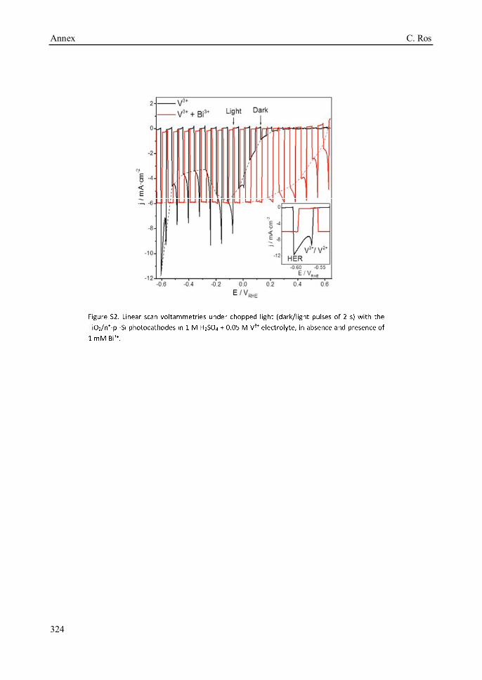
Annex C. Ros
324
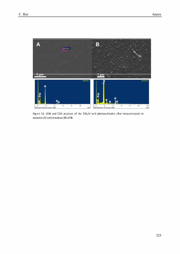
C. Ros Annex
325
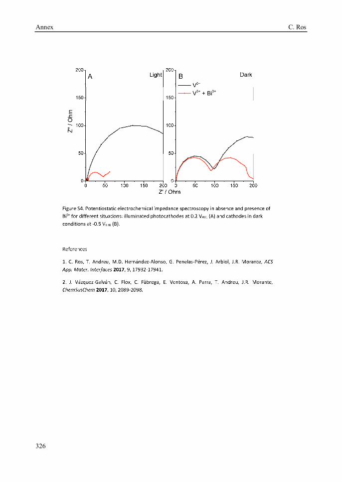
Annex C. Ros
326

C. Ros Annex
327
Figure A.3. Reprint of the WO/2017/109108 international patent.