Spray-deposited NiO x films on ITO substrates as photoactive electrodes for p-type dye-sensitized...
7
ORIGINAL PAPER Spray-deposited NiO x films on ITO substrates as photoactive electrodes for p-type dye-sensitized solar cells Muhammad Awais • Denis D. Dowling • Mahfujur Rahman • Johannes G. Vos • Franco Decker • Danilo Dini Received: 31 July 2012 / Accepted: 5 November 2012 / Published online: 30 November 2012 Ó Springer Science+Business Media Dordrecht 2012 Abstract Spray deposition followed by sintering of nickel oxide (NiO x ) nanoparticles (average diameter: 40 nm) has been chosen as method of deposition of mes- oporous NiO x coatings onto indium tin oxide (ITO) sub- strates. This procedure allows the scalable preparation of NiO x samples with large surface area (*10 3 times the geometrical area) and its potential for applications such as electrocatalysis or electrochemical solar energy conver- sion, which require high electroactivity in confined sys- tems. The potential of these NiO x films as semiconducting cathodes for dye-sensitized solar cell (DSC) purposes has been evaluated for 0.3–3-lm-thick films of NiO x sensitized with erythrosine B (ERY). The electrochemical processes involving the NiO x coatings in the pristine and sensitized states were examined and indicated surface confinement as demonstrated by the linear dependence of the current densities with the scan rate of the cyclic voltammetry. Cathodic polarization of NiO x on ITO can also lead to the irreversible reduction of the underlying ITO substrate because of the mesoporous nature of the sintered NiO x film that allows the shunting of ITO to the electrolyte. ITO- based reduction processes alter irreversibly the properties of charge transfer through the ITO/NiO x interface and limit the range of potential to NiO x coatings sintered for DSC purposes. Keywords Nickel oxide p-Type semiconductor electrode Semiconductor electrochemistry Dye-sensitized solar cell Indium tin oxide Sintering 1 Introduction Nickel oxide (NiO x with 1 \ x \ 1.5) is a p-type semicon- ductor with wide band-gap (E g [ 3.50 eV), displaying room temperature conductivity values in the order of 10 -4 – 10 -2 S cm -1 [1]. The intrinsic p-type conductivity of NiO x is mainly related to its non-stoichiometric nature where Ni 3? centers constitute the oxide defects through which holes are transferred [2]. Moreover, the oxide is characterized by high chemical stability and optical transparency when in the configuration of thin film with thickness l \ 2 lm[3, 4]. Because of this interesting combination of electrical and optical properties, NiO x has been considered as active Electronic supplementary material The online version of this article (doi:10.1007/s10800-012-0506-1) contains supplementary material, which is available to authorized users. M. Awais D. D. Dowling M. Rahman J. G. Vos D. Dini Solar Energy Conversion Strategic Research Cluster, Dublin, Ireland M. Awais Interdisciplinary Research Centre in Biomedical Materials (IRCBM), COMSATS Institute of Information Technology (CIIT), Defence Road, Off Raiwind Road, Lahore, Pakistan D. D. Dowling School of Mechanical and Materials Engineering, University College Dublin, Dublin, Ireland M. Rahman School of Chemical and Bioprocess Engineering, University College Dublin, Dublin, Ireland J. G. Vos School of Chemical Sciences, Dublin City University, Dublin, Ireland F. Decker D. Dini (&) Department of Chemistry, University of Rome ‘‘La Sapienza’’, P.le Aldo Moro 5, 00185 Rome, Italy e-mail: [email protected] 123 J Appl Electrochem (2013) 43:191–197 DOI 10.1007/s10800-012-0506-1
Transcript of Spray-deposited NiO x films on ITO substrates as photoactive electrodes for p-type dye-sensitized...

ORIGINAL PAPER
Spray-deposited NiOx films on ITO substrates as photoactiveelectrodes for p-type dye-sensitized solar cells
Muhammad Awais • Denis D. Dowling •
Mahfujur Rahman • Johannes G. Vos •
Franco Decker • Danilo Dini
Received: 31 July 2012 / Accepted: 5 November 2012 / Published online: 30 November 2012
� Springer Science+Business Media Dordrecht 2012
Abstract Spray deposition followed by sintering of
nickel oxide (NiOx) nanoparticles (average diameter:
40 nm) has been chosen as method of deposition of mes-
oporous NiOx coatings onto indium tin oxide (ITO) sub-
strates. This procedure allows the scalable preparation of
NiOx samples with large surface area (*103 times the
geometrical area) and its potential for applications such as
electrocatalysis or electrochemical solar energy conver-
sion, which require high electroactivity in confined sys-
tems. The potential of these NiOx films as semiconducting
cathodes for dye-sensitized solar cell (DSC) purposes has
been evaluated for 0.3–3-lm-thick films of NiOx sensitized
with erythrosine B (ERY). The electrochemical processes
involving the NiOx coatings in the pristine and sensitized
states were examined and indicated surface confinement
as demonstrated by the linear dependence of the current
densities with the scan rate of the cyclic voltammetry.
Cathodic polarization of NiOx on ITO can also lead to the
irreversible reduction of the underlying ITO substrate
because of the mesoporous nature of the sintered NiOx film
that allows the shunting of ITO to the electrolyte. ITO-
based reduction processes alter irreversibly the properties
of charge transfer through the ITO/NiOx interface and limit
the range of potential to NiOx coatings sintered for DSC
purposes.
Keywords Nickel oxide � p-Type semiconductor
electrode � Semiconductor electrochemistry �Dye-sensitized solar cell � Indium tin oxide �Sintering
1 Introduction
Nickel oxide (NiOx with 1 \ x \ 1.5) is a p-type semicon-
ductor with wide band-gap (Eg [ 3.50 eV), displaying room
temperature conductivity values in the order of 10-4–
10-2 S cm-1 [1]. The intrinsic p-type conductivity of NiOx
is mainly related to its non-stoichiometric nature where Ni3?
centers constitute the oxide defects through which holes
are transferred [2]. Moreover, the oxide is characterized by
high chemical stability and optical transparency when in the
configuration of thin film with thickness l \ 2 lm [3, 4].
Because of this interesting combination of electrical and
optical properties, NiOx has been considered as active
Electronic supplementary material The online version of thisarticle (doi:10.1007/s10800-012-0506-1) contains supplementarymaterial, which is available to authorized users.
M. Awais � D. D. Dowling � M. Rahman � J. G. Vos � D. Dini
Solar Energy Conversion Strategic Research Cluster, Dublin,
Ireland
M. Awais
Interdisciplinary Research Centre in Biomedical Materials
(IRCBM), COMSATS Institute of Information Technology
(CIIT), Defence Road, Off Raiwind Road, Lahore, Pakistan
D. D. Dowling
School of Mechanical and Materials Engineering,
University College Dublin, Dublin, Ireland
M. Rahman
School of Chemical and Bioprocess Engineering,
University College Dublin, Dublin, Ireland
J. G. Vos
School of Chemical Sciences, Dublin City University, Dublin,
Ireland
F. Decker � D. Dini (&)
Department of Chemistry, University of Rome ‘‘La Sapienza’’,
P.le Aldo Moro 5, 00185 Rome, Italy
e-mail: [email protected]
123
J Appl Electrochem (2013) 43:191–197
DOI 10.1007/s10800-012-0506-1

material for various applications like energy storage, [5, 6]
electrochromic smart windows, [7–11] optoelectronic devi-
ces [12], and, more importantly, dye-sensitized solar cells
(DSCs) as photoactive dye-sensitized mesoporous cathode
[13–19]. The utilization of NiOx in such diverse applications
has been accompanied by the development of various prep-
aration methods and deposition techniques aimed at pro-
ducing NiOx-based materials with variable chemical
composition, electrical resistivity, compactness, and mor-
phology for performance optimization. Most common
examples include sputtering [20], electrochemical deposi-
tion [21], spray pyrolysis [22] or sol–gel method [13, 23, 24].
In the present study, we have considered the fabrication of
NiOx thin films (0.2 \ l \ 3 lm) for DSC purposes through
the thermal sintering of spray-deposited NiOx nanoparticles
(average diameter 40 nm) onto indium–tin oxide (ITO)
substrates. The determination of the morphological, elec-
trochemical, and photo-electrochemical properties of NiOx
films in the bare state and in the sensitized version with dye
erythrosine B (ERY) [13, 24] has been accomplished toge-
ther with the analysis of the electrochemical processes
occurring in uncoated ITO substrates [25–27]. This approach
allows for the critical evaluation of the factors regulating the
performance of the DSCs based on photoactive cathodes of
sintered NiOx when deposited onto ITO through a scalable
method.
2 Experimental
2.1 Deposition of NiOx coatings
NiOx nanoparticles, with an average particle size of 40 nm
(from Sigma-Aldrich), were suspended in 2-propanol
(concentration: 20 mg/mL). A loosely adherent particulate
layer of NiOx was then deposited from this suspension by
spray deposition, using a technique similar to that descri-
bed previously by Halme et al. [28, 29]. The nanoparticle
layer was deposited onto unheated ITO-coated glass panels
(5 9 5 cm2) obtained from Balzers. The NiOx nanoparti-
cles on the conducting glass substrate were sintered for
30 min using a Carbolite Furnace (RHF 1200), in air at
450 �C [28]. This thermal treatment affords the connection
of the NiOx nanoparticles and warrants the electrical con-
tact between nanoparticles and at the NiOx/ITO interface.
By controlling the duration of spraying, the thickness of the
NiOx nanoparticulate coatings on the ITO glass substrates
was controlled as required in the range of 0.3–3 lm.
2.2 Morphology characterization equipment
The cross-sectional investigations of the NiOx coating
were carried out using a FEI Quanta 3D FEG DaulBeamTM
(FEI Ltd., Hillsboro, USA) focused ion beam/scanning elec-
tron microscope (FIB/SEM) system. Before SEM analyses,
the deposited NiOx films were coated with platinum via
sputtering using an Emitech K575X sputter coating unit. This
was done to prevent surface charging by the electron beam.
2.3 Sensitization of NiOx coatings
NiOx coatings were sensitized with ERY from Sigma-Aldrich
(kMAX: 535 nm), by dipping the oxide film in a 0.3 mM
solution of the dye in 99.8 % ethanol (from Fisher) for 24 h at
room temperature. After removing the electrode from tincture
solution, the sensitized electrode was washed with pure
ethanol to remove the non-chemisorbed dye molecules.
2.4 Electrochemical characterization of uncoated ITO
Before the electrochemical cycling, the uncoated ITO
substrate was cleaned in an ultrasonic bath (solvent: iso-
propyl alcohol) for 30 min and then dried in an oven at
60 �C. After this cleaning treatment, the ITO substrate was
placed in the Ar-filled glove box. The uncoated ITO sub-
strate was manipulated in the glove-box for cell assembly.
2.5 Electrochemical characterization of NiOx coatings
The electrochemical cell had a three-electrode configuration
[30] with glass/ITO/NiOx or dye-sensitized NiOx as working
electrode, Li rod (from Sigma-Aldrich) as counter electrode,
and Li/LiClO4 [0.7 M in anhydrous propylene carbonate
(PC) from Fisher] as reference electrode. All potential values
in this study are referred to the Li?/Li redox couple [31].
Electrolyte was 0.7 M LiClO4 in anhydrous PC. Supporting
electrolyte LiClO4 was purchased from Aldrich and was not
pre-treated before use. Chemicals were stored in an Ar-filled
glove-box (Innovative Technology, Newburyport, MA,
USA), with O2 and H2O contents being below 10 and 5 ppm,
respectively. The electrochemical cells were assembled
under Ar atmosphere inside the glove-box, and a supernatant
Ar atmosphere was maintained in the cell during the elec-
trochemical experiments with bare and sensitized NiOx
samples. Cyclic voltammetries were carried out using an
electrochemical analyzer (model 604C) from CH Instru-
ments (Austin, TX, USA).
2.6 DSC preparation
The sensitized films (see Sect. 2.3) were sealed face-to-face
in a sandwich configuration with a platinized fluorine-
doped tin oxide (FTO) counter electrode using 30-lm-thick
pre-cut Surlyn thermoplastic frame (6 9 6 mm2 interior)
similar to what is reported in ref [32]. The sandwiched
device was filled with 0.1 M I2 and 1.0 M LiI in
192 J Appl Electrochem (2013) 43:191–197
123

acetonitrile electrolyte through a pre-drilled hole in the
counter electrode using an insertion procedure at reduced
pressure [33]. The hole was sealed with Surlyn and a glass
cover-slide.
3 Results and discussion
3.1 Electrochemical behavior of sintered NiOx coating
on ITO
The SEM images of a 2.7-micron-thick sample (Figs. 1, 2)
demonstrate that the NiOx coatings on ITO deposited using
the spray technique, followed by furnace sintering, exhibit
a relatively rough surface morphology and mesoporous
features.
The NiOx film deposited onto ITO via conventional sin-
tering of 40 nm diameter oxide nanoparticles [28] presents a
voltammogram typical of NiOx thin coatings with two broad
oxidation waves in the interval 2.75–3.75 V versus Li?/Li
[34], and lithium ions intercalation in the potential range of
1–2.5 V versus Li?/Li [35, 36] (Fig. 3, first cycle).
Continuous cycling in the extended potential range of
1–4 V versus Li?/Li leads to the loss of any electro-
chemical feature characteristic of NiOx oxidation
(E [ 2.5 V versus Li?/Li) and to the thorough modifica-
tion of the shape of the reduction peak (Fig. 3). This
indicates that n-type ITO modifies its electron transfer
properties upon electrochemical cycling [37] also in non-
aqueous electrolyte because of the direct contact of ITO
with the electrolyte. Such a shunt effect is due to the porous
nature of the sintered NiOx coating (Figs. 1, 2), which
allows for the formation of the ITO/electrolyte interface.
The electrochemical behavior of uncoated ITO in 0.7 M
LiClO4-PC (sheet resistance: 15 X/h, thickness: 0.1 lm)
in oxygen- and water-free atmosphere has been examined
within the potential window of 1.2–3.7 V versus Li?/Li to
check the electroactivity of the bare substrate. The first
voltammogram of ITO (Fig. 4) presents a broad reduction
peak centered at about 1.75 V versus Li?/Li, which is
accompanied by a second reduction process at about 1.2 V
versus Li?/Li (sharp peak).
Fig. 1 SEM image showing the surface morphology of a NiOx layer
(l = 2–3 lm) deposited onto ITO via sintering of nanoparticles with
diameter values distributed between 30 and 90 nm (evidenced in
yellow). (Color figure online)
Fig. 2 Dual beam FIB–SEM image showing the cross section of a
NiOx layer (l = 2–3 lm) deposited onto ITO via conventional
sintering of nanoparticles with average diameter of 40 nm (Fig. 1).
Yellow arrow indicates the thickness of the NiO film. (Color figure
online)
1,0 1,5 2,0 2,5 3,0 3,5
-1,0x10⁻⁴
-5,0x10⁻⁵
0,0
5,0x10⁻⁵
J / A
cm
-2
E / V vs Li+/Li
1st cycle 50th cycle
Fig. 3 Effect of electrochemical cycling on the voltammogram of
NiOx-coated ITO (scan rate: 15 mV s-1). Electrolyte: 0.7 M LiClO4
in anhydrous PC; counter electrode: Li; reference redox couple:
Li?/Li. Thickness of NiOx coating: 0.3 lm
J Appl Electrochem (2013) 43:191–197 193
123
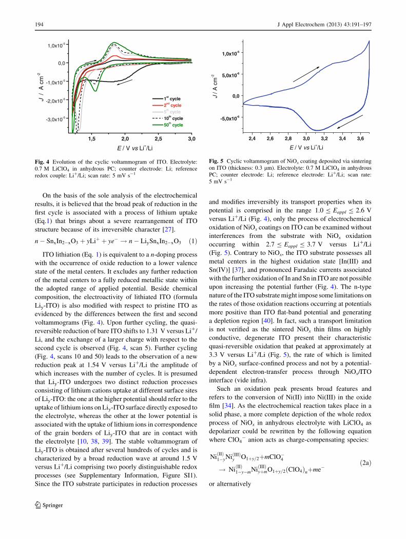
On the basis of the sole analysis of the electrochemical
results, it is believed that the broad peak of reduction in the
first cycle is associated with a process of lithium uptake
(Eq.1) that brings about a severe rearrangement of ITO
structure because of its irreversible character [27].
n� SnxIn2�xO3 þ yLiþ þ ye� ! n� LiySnxIn2�xO3 ð1Þ
ITO lithiation (Eq. 1) is equivalent to a n-doping process
with the occurrence of oxide reduction to a lower valence
state of the metal centers. It excludes any further reduction
of the metal centers to a fully reduced metallic state within
the adopted range of applied potential. Beside chemical
composition, the electroactivity of lithiated ITO (formula
Liy-ITO) is also modified with respect to pristine ITO as
evidenced by the differences between the first and second
voltammograms (Fig. 4). Upon further cycling, the quasi-
reversible reduction of bare ITO shifts to 1.31 V versus Li?/
Li, and the exchange of a larger charge with respect to the
second cycle is observed (Fig. 4, scan 5). Further cycling
(Fig. 4, scans 10 and 50) leads to the observation of a new
reduction peak at 1.54 V versus Li?/Li the amplitude of
which increases with the number of cycles. It is presumed
that Liy-ITO undergoes two distinct reduction processes
consisting of lithium cations uptake at different surface sites
of Liy-ITO: the one at the higher potential should refer to the
uptake of lithium ions on Liy-ITO surface directly exposed to
the electrolyte, whereas the other at the lower potential is
associated with the uptake of lithium ions in correspondence
of the grain borders of Liy-ITO that are in contact with
the electrolyte [10, 38, 39]. The stable voltammogram of
Liy-ITO is obtained after several hundreds of cycles and is
characterized by a broad reduction wave at around 1.5 V
versus Li?/Li comprising two poorly distinguishable redox
processes (see Supplementary Information, Figure SI1).
Since the ITO substrate participates in reduction processes
and modifies irreversibly its transport properties when its
potential is comprised in the range 1.0 B Eappl B 2.6 V
versus Li?/Li (Fig. 4), only the process of electrochemical
oxidation of NiOx coatings on ITO can be examined without
interferences from the substrate with NiOx oxidation
occurring within 2.7 B Eappl B 3.7 V versus Li?/Li
(Fig. 5). Contrary to NiOx, the ITO substrate possesses all
metal centers in the highest oxidation state [In(III) and
Sn(IV)] [37], and pronounced Faradaic currents associated
with the further oxidation of In and Sn in ITO are not possible
upon increasing the potential further (Fig. 4). The n-type
nature of the ITO substrate might impose some limitations on
the rates of those oxidation reactions occurring at potentials
more positive than ITO flat-band potential and generating
a depletion region [40]. In fact, such a transport limitation
is not verified as the sintered NiOx thin films on highly
conductive, degenerate ITO present their characteristic
quasi-reversible oxidation that peaked at approximately at
3.3 V versus Li?/Li (Fig. 5), the rate of which is limited
by a NiOx surface-confined process and not by a potential-
dependent electron-transfer process through NiOx/ITO
interface (vide infra).
Such an oxidation peak presents broad features and
refers to the conversion of Ni(II) into Ni(III) in the oxide
film [34]. As the electrochemical reaction takes place in a
solid phase, a more complete depiction of the whole redox
process of NiOx in anhydrous electrolyte with LiClO4 as
depolarizer could be rewritten by the following equation
where ClO4- anion acts as charge-compensating species:
NiðIIÞ1�yNiðIIIÞy O1þy=2þmClO�4
! NiðIIÞ1�y�mNi
ðIIIÞyþmO1þy=2 ClO4ð Þnþme�
ð2aÞ
or alternatively
1,5 2,0 2,5 3,0
-3,0x10⁻⁵
-2,0x10⁻⁵
-1,0x10⁻⁵
0,0
1,0x10⁻⁵J
/ A
cm
-2
E / V vs Li+/Li
1st cycle 2nd cycle 5th cycle 10th cycle 50th cycle
Fig. 4 Evolution of the cyclic voltammogram of ITO. Electrolyte:
0.7 M LiClO4 in anhydrous PC; counter electrode: Li; reference
redox couple: Li?/Li; scan rate: 5 mV s-1
2,4 2,6 2,8 3,0 3,2 3,4 3,6
-5,0x10⁻⁶
0,0
5,0x10⁻⁶
1,0x10⁻⁵
J / A
cm
-2
E / V vs Li+/Li
Fig. 5 Cyclic voltammogram of NiOx coating deposited via sintering
on ITO (thickness: 0.3 lm). Electrolyte: 0.7 M LiClO4 in anhydrous
PC; counter electrode: Li; reference electrode: Li?/Li; scan rate:
5 mV s-1
194 J Appl Electrochem (2013) 43:191–197
123
NiOx OHð Þm! NiOxþ1 OHð Þm�1þe� þ Hþ ð2bÞ
if nickel oxide is considered a mixture of oxide and
hydroxide [34]. In both the cases, the electroactive NiOx
film is supposed to contain nickel ions in both the oxidation
states ?2 and ?3. In fact, the onset of NiO oxidation is
about 2.85 V versus Li?/Li. This indicates that the pristine
film of sintered NiOx already contains a fraction of Ni(III)
sites because of the open circuit voltage (VOC) of the cell
Glass=ITO=NiOx== 0:7 M LiClO4 in PC == Li; Ref
: Li=LiClO4 0:7 M in PCð Þ ðaÞ
is 3.07 V versus Li?/Li, i.e., a value which is above the
onset of Ni(II) site oxidation. When the scan rate depen-
dence of the more resolved reduction peak of sintered NiOx
is analyzed (Fig. 6), a linear relationship between peak
height and scan rate is found (see Supplementary Infor-
mation, Figure SI4).
This corresponds to the occurrence of a surface-confined
redox process [41], the rate of which does not depend on
the diffusion of charge carriers or mass transfer processes
(vide supra), and this is consistent with the previous data
presented by Boschloo et al. [34] who examined NiOx
samples prepared via the sol–gel method.
3.2 Photo-electrochemical characterization
of ERY-sensitized NiOx
The porous nature of the NiOx coatings deposited via sin-
tering of oxide nanoparticles (Fig. 1) renders possible the
efficacious sensitization of the oxide with a visible light
absorber. In the present study, erythrosine B (ERY) has been
considered as dye sensitizer because of the matching of its
frontier energy levels with the band edges of p-type NiOx.
[13, 24, 28, 42] Dye sensitization of the sintered NiOx sample
with ERY generally leads to a small decrease of the dark
current densities (Fig. 7), with respect to the corresponding
curves of bare nickel oxide samples (Fig. 6). Moreover,
current peaks associated with ERY-based electrochemical
processes are not introduced in the voltammogram of ERY-
sensitized NiOx deposited on ITO substrates within the
experimental range of applied potential.
Therefore, ERY layer behaves as an electrochemically
inert layer, with no involvement in any of the observed
faradic processes. Illumination of the dye-sensitized oxide
samples with white light produces a positive photo-poten-
tial, an increase of the oxidation current density, and the
negative shift of the current baseline when no redox pro-
cesses occur (Fig. 7). These facts can be explained in terms
of photogeneration of positive charge carriers in dye-sen-
sitized nickel oxide when visible light is absorbed by ERY
layer (photoconductive effect) [13, 24, 42]. Cyclic vol-
tammetries of ERY-sensitized NiOx have been carried out
at different scan rates in the dark and under white light
illumination (see Supplementary Information, Figures SI5
and SI6) to evaluate the characteristics of the dark and
photo-oxidation process of NiOx when sensitized.
The cathodic peak referring to the reverse process
Ni(III)? Ni(II) (reverse of processes in Eq.2) has been
considered for analysis because of its generally better
resolution with respect to the correlated anodic peak which
displays broader features in the voltammogram. Similar to
bare NiOx, both the dark and photo-electrochemical oxi-
dation processes of ERY-sensitized NiOx present the typ-
ical features of a surface-confined redox process being the
current peaks directly proportional to the scan rate (see
Supplementary Information, Figure SI7).
2,4 2,6 2,8 3,0 3,2 3,4 3,6-4,0x10⁻⁵
-2,0x10⁻⁵
0,0
2,0x10⁻⁵
4,0x10⁻⁵J
/ A c
m-2
E / V vs Li+/Li
5 mV s-1
10 mV s-1
20 mV s-1
40 mV s-1
65 mV s-1
Fig. 6 Cyclic voltammograms of the NiOx coating (thickness:
0.3 lm) deposited via sintering of NiOx nanoparticles on ITO at
different scan rates. Cell configuration is the same as in Fig. 5. Bluearrows indicate the direction of potential scan. (Color figure online)
2,4 2,6 2,8 3,0 3,2 3,4 3,6
-4,0x10⁻⁶
0,0
4,0x10⁻⁶
8,0x10⁻⁶
J /
A c
m-2
E / V vs Li+/Li
5 mV s-1
5 mV s-1 - light ON
Fig. 7 Cyclic voltammograms the of ERY-sensitized NiOx coating
(thickness: 0.3 lm) in the dark and under illumination with whitelight (Pin = 50 W) from a halogen lamp. Electrolyte composition as
in Fig. 5. Electrode area: 1.75 cm2. Arrows indicate the direction of
potential scan
J Appl Electrochem (2013) 43:191–197 195
123
ERY-sensitized NiOx on ITO has been utilized as pho-
toactive electrode in a cathodic DSC [24] with platinized
FTO as counter electrode. The photocathode and the
counter electrode had the same electroactive area in the
DSC. The electrolyte was a solution of the redox couple
I3-/I- in acetonitrile. The characteristic curve of the NiOx-
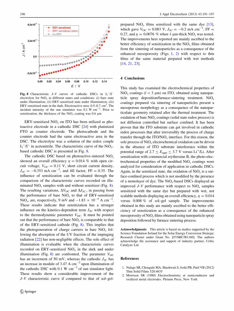
based cathodic DSC is presented in Fig. 8.
The cathodic DSC based on photoactive-sintered NiOx
showed an overall efficiency g = 0.014 % with open cir-
cuit voltage, VOC = 0.11 V, short circuit current density,
JSC = -0.353 mA cm-2, and fill factor, FF = 0.35. The
influence of sensitization can be evaluated through the
comparison of the characteristic curves recorded on illu-
minated NiOx samples with and without sensitizer (Fig. 8).
The resulting variations, DVOC and DJSC,, in passing from
the performance of bare NiOx to that of ERY-sensitized
NiOx, are, respectively, 9 mV and -1.83 9 10-4 A cm-2.
These results indicate that sensitization has a stronger
influence on the kinetics-dependent term JSC with respect
to the thermodynamic parameter VOC. It must be pointed
out that the performance of bare NiOx is comparable to that
of the ERY-sensitized cathode (Fig. 8). This implies that
the photogeneration of charge carriers in bare NiOx fol-
lowing the absorption of the UV fraction of the impinging
radiation [22] has non-negligible effects. The sole effect of
illumination is evaluable when the characteristic curves
recorded on ERY-sensitized NiOx in the dark and under
illumination (Fig. 8) are confronted. The parameter VOC
has an increment of 50 mV, whereas the cathodic JSC has
an increase in module of 3.47 A cm-2 upon illumination of
the cathodic DSC with 0.1 W cm-2 of sun simulator light.
These results show a considerable improvement of the
J–V characteristic curve if compared to that of sol–gel-
prepared NiOx films sensitized with the same dye [13],
which gave VOC = 0.083 V, JSC = -0.2 mA cm-2, FF =
0.27, and g = 0.0076 % when 1-lm-thick NiOx was tested.
The improvements here reported are mainly ascribed to the
better efficiency of sensitization in the NiOx films obtained
from the sintering of nanoparticles as a consequence of the
enhanced mesoporosity (Figs. 1, 2) with respect to thin
films of the same material prepared with wet methods
[14, 21, 23].
4 Conclusions
This study has examined the electrochemical properties of
NiOx coatings (l \ 3 lm) on ITO, obtained using nanopar-
ticle spray deposition/furnace-sintering treatment. NiOx
coatings prepared via sintering of nanoparticles present a
mesoporous morphology as a consequence of the nanopar-
ticulate geometry retained after the thermal treatment. The
oxidation of bare NiOx coatings (solid state redox process) is
not diffusion controlled but surface confined. It has been
proven that the ITO substrate can get involved in cathodic
redox processes that alter irreversibly the process of charge
transfer through the ITO/NiOx interface. For this reason, the
sole process of NiOx electrochemical oxidation can be driven
in the absence of ITO substrate interference within the
potential range of 2.7 B Eappl B 3.7 V versus Li?/Li. After
sensitization with commercial erythrosine B, the photo-elec-
trochemical properties of the modified NiOx coatings were
analyzed for consideration of application in cathodic DSCs.
Again, in the sensitized state, the oxidation of NiOx is a sur-
face-confined process which is not modified by the presence
of a monolayer of dye. The NiOx-based DSCs displayed an
improved J–V performance with respect to NiOx samples
sensitized with the same dye but prepared with wet, not
scalable methods displaying an overall efficiency, g = 0.014
versus 0.008 % of sol–gel sample. The improvements
obtained in this study are mainly ascribed to the better effi-
ciency of sensitization as a consequence of the enhanced
mesoporosity of NiOx films obtained using nanoparticle spray
deposition followed by furnace sintering process.
Acknowledgments This article is based on studies supported by the
Science Foundation Ireland for the Solar Energy Conversion Strategic
Research Cluster under Grant No. [07/SRC/B1160]. The authors
acknowledge the assistance and support of industry partner, Celtic
Catalysts Ltd.
References
1. Nalage SR, Chougule MA, Shashwati S, Joshi PB, Patil VB (2012)
Thin Solid Films 520:4835
2. Morrison SR (1980) Electrochemistry at semiconductor and
oxidized metal electrodes. Plenum Press, New York
0,00 0,02 0,04 0,06 0,08 0,10 0,12 0,14
-3,0x10⁻⁴
0,0
3,0x10⁻⁴
6,0x10⁻⁴J
/ A c
m-2
E / V
ERY sensitizedERY sensitised (dark)no ERY
Fig. 8 Characteristic J–V curves of cathodic DSCs in I3-/I-
electrolyte for NiOx in different states and conditions: (i) bare state
under illumination; (ii) ERY-sensitized state under illumination; (iii)
ERY-sensitized state in the dark. Electroactive area: 0.5–0.7 cm2. The
incident intensity of the sun simulator was 0.1 W cm-2. Prior to
sensitization, the thickness of the NiOx coating was 0.6 lm
196 J Appl Electrochem (2013) 43:191–197
123

3. Sato H, Minami T, Takata S, Yamada T (1993) Thin Solid Films
236:27
4. Granqvist CG (2007) Sol Energy Mater Sol Cells 91:1529
5. Nam KW, Yoon WS, Kim KB (2002) Electrochim Acta 47:3201
6. Lang JW, Kong LB, Liu M, Luo YC, Kang L (2010) J Solid State
Electrochem 14:1533
7. Estrada W, Andersson AM, Granqvist CG, Gorenstein A, Decker
F (1991) J Mater Res 6:1715
8. Svegl F, Surca-Vuk A, Hajzeri M, Slemenik-Perse L, Orel B Sol
(2012) Energy Mater Sol Cells 99:14
9. Avendano A, Azens A, Niklasson GA, Granqvist CG (2007)
Mater Sci Eng B 138:112
10. Huang H, Tian J, Zhang WK, Gan YP, Tao XY, Xia XH, Tu JP
(2011) Electrochim Acta 56:4281
11. Gillaspie D, Norman A, Tracy CE, Pitts JR, Lee SH, Dillon A
(2010) J Electrochem Soc 157:H328
12. Irwin MD, Buchholz DB, Hains AW, Chang RPH, Marks TJ
(2008) Proc Nat Acad Sci 105:2783
13. He J, Lindstrom H, Hagfeldt A, Lindquist SE (1999) J Phys Chem
B 103:8940
14. Nakasa A, Usami H, Sumikura S, Hasegawa S, Koyama T,
Suzuki E (2005) Chem Lett 34:500
15. Morandeira A, Boschloo G, Hagfeldt A, Hammarstrom L (2008)
J Phys Chem C 112:9530
16. Nattestad A, Ferguson M, Kerr R, Cheng YB, Bach U (2008)
Nanotechnology 19:295304
17. Qin P, Zhu H, Edvinsson T, Boschloo G, Hagfeldt A, Sun L
(2008) J Am Chem Soc 130:8570
18. Li L, Gibson EA, Qin P, Boschloo G, Gorlov M, Hagfeldt A,
Sun L (2010) Adv Mater 22:1759
19. Nattestad A, Mozer AJ, Fischer MKR, Cheng YB, Mishra A,
Bauerle P, Bach U (2010) Nature Mater 9:31
20. Awais M, Rahman M, MacElroy JMD, Coburn N, Dini D, Vos
JG, Dowling DP (2010) Surf Coat Technol 204:2729
21. Wu MS, Wang MJ (2010) Chem Commun 46:6968
22. Garduno IA, Alonso JC, Bizarro M, Ortega R, Rodrıguez-Fern-
andez L, Ortiz A (2010) J Cryst Growth 312:3276
23. Jiao Z, Wu M, Qin Z, Xu H (2003) Nanotechnology 14:458
24. He J, Lindstrom H, Hagfeldt A, Lindquist SE (2000) Sol Energy
Mater Sol Cells 62:265
25. Cogan SF, Anderson EJ, Plante TD, Rauh RD (1985) Appl Opt
24:2282
26. Bressers PMMC, Meulenkamp EA (1998) J Electrochem Soc
145:2225
27. Wang Z, Hu X (2001) Thin Solid Films 392:22
28. Awais M, Rahman M, MacElroy JMD, Dini D, Vos JG, Dowling
DP (2011) Surf Coat Technol 205:S245
29. Halme J, Saarinen J, Lund P (2006) Sol Energy Mater Sol Cells
90:887
30. Decker F, Passerini S, Pileggi R, Scrosati B (1992) Electrochim
Acta 37:1033
31. Masetti E, Dini D, Decker F (1995) Sol Energy Mater Sol Cells
39:301
32. Gibson EA, Smeigh AL, Le Pleux L, Fortage J, Boschloo G,
Blart E, Pellegrin Y, Odobel F, Hagfeldt A, Hammarstrom (2009)
Angew Chem Int Ed 48:4402
33. Mastroianni S, Lanuti A, Penna S, Reale A, Brown TM, Di Carlo
A, Decker F (2012) ChemPhysChem, to be published
34. Boschloo G, Hagfeldt A (2001) J Phys Chem B 105:3039
35. Passerini S, Scrosati B, Gorenstein A (1990) J Electrochem Soc
137:3297
36. Passerini S, Scrosati B (1994) J Electrochem Soc 141:889
37. Armstrong NA, Lin AWC, Masamichi F, Kuwana T (1976) Anal
Chem 48:741
38. Chippindale AM, Dickens PG, Powell AV (1991) Prog Solid St
Chem 21:133
39. Whittingham MS, Chen R, Chirayil T, Zavalij P (1997) Solid
State Ionics 94:227
40. Gerischer H (1990) Electrochim Acta 35:1677
41. Bard AJ, Faulkner LR (2001) Electrochemical methods (funda-
mentals and applications), 2nd edn. John Wiley, New York, p 595
42. Vera F, Schrebler R, Munoz E, Suarez C, Cury P, Gomez H,
Cordova R, Marotti RE, Dalchiele EA (2005) Thin Solid Films
490:182
J Appl Electrochem (2013) 43:191–197 197
123


![Impedance spectroscopic investigations of ITO modified by new Azo-calix[4]arene immobilised into electroconducting polymer (MEHPPV)](https://static.fdokumen.com/doc/165x107/634532ab596bdb97a908d170/impedance-spectroscopic-investigations-of-ito-modified-by-new-azo-calix4arene.jpg)
![An amperometric uric acid biosensor based on Bis[sulfosuccinimidyl] suberate crosslinker/3-aminopropyltriethoxysilane surface modified ITO glass electrode](https://static.fdokumen.com/doc/165x107/63129cf1fc260b71020eb9f6/an-amperometric-uric-acid-biosensor-based-on-bissulfosuccinimidyl-suberate-crosslinker3-aminopropyltriethoxysilane.jpg)