Spatially confined synthesis of SiOx nano-rod with size-controlled Si quantum dots in nano-porous...
10
Spatially confined synthesis of SiO x nano-rod with size-controlled Si quantum dots in nano-porous anodic aluminum oxide membrane Yi-Hao Pai 1,2 and Gong-Ru Lin 1, * 1 Institute of Photonics and Optoelectronics, Department of Electrical Engineering, National Taiwan University No.1 Roosevelt Rd. Sec. 4, Taipei 10617, Taiwan 2 Department of Opto-Electronic Engineering, National Dong Hwa University No. 1, Sec. 2, Da Hsueh Rd., Shoufeng, Hualien, 97401, Taiwan *[email protected] Abstract: By depositing Si-rich SiO x nano-rod in nano-porous anodic aluminum oxide (AAO) membrane using PECVD, the spatially confined synthesis of Si quantum-dots (Si-QDs) with ultra-bright photoluminescence spectra are demonstrated after low-temperature annealing. Spatially confined SiO x nano-rod in nano-porous AAO membrane greatly increases the density of nucleated positions for Si-QD precursors, which essentially impedes the route of thermally diffused Si atoms and confines the degree of atomic self-aggregation. The diffusion controlled growth mechanism is employed to determine the activation energy of 6.284 kJ mole 1 and diffusion length of 2.84 nm for SiO 1.5 nano-rod in nano-porous AAO membrane. HRTEM results verify that the reduced geometric dimension of the SiO x host matrix effectively constrain the buried Si-QD size at even lower annealing temperature. The spatially confined synthesis of Si-QD essentially contributes the intense PL with its spectral linewidth shrinking from 210 to 140 nm and its peak intensity enhancing by two orders of magnitude, corresponding to the reduction on both the average Si-QD size and its standard deviation from 2.6 to 2.0 nm and from 25% to 12.5%, respectively. The red-shifted PL wavelength of the Si-QD reveals an inverse exponential trend with increasing temperature of annealing, which is in good agree with the Si-QD size simulation via the atomic diffusion theory. ©2011 Optical Society of America OCIS codes: (160.4236) Nanomaterials; (250.5230) Photoluminescence; (310.1860) Deposition and fabrication. References and links 1. M. Lopez, B. Garrido, C. Garcia, P. Pellegrino, A. Perez-Rodriguez, J. R. Morante, C. Bonafos, M. Carrada, and A. Claverie, “Elucidation of the surface passivation role on the photoluminescence emission yield of silicon nanocrystals embedded in SiO2,” Appl. Phys. Lett. 80, 1637–1639 (2002). 2. S. Kim, M. C. Kim, S. H. Choi, K. J. Kim, H. N. Hwang, and C. C. Hwang, “Size dependence of Si 2p core-level shift at Si nanocrystal/SiO2 interfaces,” Appl. Phys. Lett. 91(10), 103113 (2007). 3. C. H. Lin, S. C. Lee, and Y. F. Chen, “Strong room-temperature photoluminescence of hydrogenated amorphous-silicon oxide and its correlation to porous silicon,” Appl. Phys. Lett. 63(7), 902–904 (1993). 4. F. Baumann, B. Deubzer, M. Geck, J. Dauth, S. Sheiko, and M. Schmidt, “Soluble organosilicon micronetworks with spatially confined reaction sites,” Adv. Mater. 9(12), 955–958 (1997). 5. Q. Cheng, S. Xu, and K. Ostrikov, “Single-step, rapid low-temperature synthesis of Si quantum dots embedded in an amorphous SiC matrix in high-density reactive plasmas,” Acta Mater. 58(2), 560–569 (2010). 6. Q. Cheng, S. Xu, S. Huang, and K. Ostrikov, “Effective control of nanostructured phases in rapid, room-temperature synthesis of nanocrystalline Si in high-density plasmas,” Cryst. Growth Des. 9(6), 2863–2867 (2009). 7. N. W. Liu, C. Y. Liu, H. H. Wang, C. F. Hsu, M. Y. Lai, T. H. Chuang, and Y. L. Wang, “Focused-ion-beam-based selective closing and opening of anodic alumina nanochannels for the growth of nanowire arrays comprising multiple elements,” Adv. Mater. 20(13), 2547–2551 (2008). #132236 - $15.00 USD Received 23 Jul 2010; revised 13 Aug 2010; accepted 14 Aug 2010; published 7 Jan 2011 (C) 2011 OSA 17 January 2011 / Vol. 19, No. 2 / OPTICS EXPRESS 896
Transcript of Spatially confined synthesis of SiOx nano-rod with size-controlled Si quantum dots in nano-porous...
Spatially confined synthesis of SiOx nano-rod
with size-controlled Si quantum dots in
nano-porous anodic aluminum oxide membrane
Yi-Hao Pai1,2
and Gong-Ru Lin1,*
1Institute of Photonics and Optoelectronics, Department of Electrical Engineering, National Taiwan University No.1 Roosevelt Rd. Sec. 4, Taipei 10617, Taiwan
2Department of Opto-Electronic Engineering, National Dong Hwa University
No. 1, Sec. 2, Da Hsueh Rd., Shoufeng, Hualien, 97401, Taiwan *[email protected]
Abstract: By depositing Si-rich SiOx nano-rod in nano-porous anodic
aluminum oxide (AAO) membrane using PECVD, the spatially confined
synthesis of Si quantum-dots (Si-QDs) with ultra-bright photoluminescence
spectra are demonstrated after low-temperature annealing. Spatially confined
SiOx nano-rod in nano-porous AAO membrane greatly increases the density
of nucleated positions for Si-QD precursors, which essentially impedes the
route of thermally diffused Si atoms and confines the degree of atomic
self-aggregation. The diffusion controlled growth mechanism is employed to
determine the activation energy of 6.284 kJ mole1
and diffusion length of
2.84 nm for SiO1.5 nano-rod in nano-porous AAO membrane. HRTEM
results verify that the reduced geometric dimension of the SiOx host matrix
effectively constrain the buried Si-QD size at even lower annealing
temperature. The spatially confined synthesis of Si-QD essentially
contributes the intense PL with its spectral linewidth shrinking from 210 to
140 nm and its peak intensity enhancing by two orders of magnitude,
corresponding to the reduction on both the average Si-QD size and its
standard deviation from 2.6 to 2.0 nm and from 25% to 12.5%, respectively.
The red-shifted PL wavelength of the Si-QD reveals an inverse exponential
trend with increasing temperature of annealing, which is in good agree with
the Si-QD size simulation via the atomic diffusion theory.
©2011 Optical Society of America
OCIS codes: (160.4236) Nanomaterials; (250.5230) Photoluminescence; (310.1860) Deposition
and fabrication.
References and links
1. M. Lopez, B. Garrido, C. Garcia, P. Pellegrino, A. Perez-Rodriguez, J. R. Morante, C. Bonafos, M. Carrada, and A.
Claverie, “Elucidation of the surface passivation role on the photoluminescence emission yield of silicon
nanocrystals embedded in SiO2,” Appl. Phys. Lett. 80, 1637–1639 (2002). 2. S. Kim, M. C. Kim, S. H. Choi, K. J. Kim, H. N. Hwang, and C. C. Hwang, “Size dependence of Si 2p core-level
shift at Si nanocrystal/SiO2 interfaces,” Appl. Phys. Lett. 91(10), 103113 (2007).
3. C. H. Lin, S. C. Lee, and Y. F. Chen, “Strong room-temperature photoluminescence of hydrogenated amorphous-silicon oxide and its correlation to porous silicon,” Appl. Phys. Lett. 63(7), 902–904 (1993).
4. F. Baumann, B. Deubzer, M. Geck, J. Dauth, S. Sheiko, and M. Schmidt, “Soluble organosilicon micronetworks
with spatially confined reaction sites,” Adv. Mater. 9(12), 955–958 (1997). 5. Q. Cheng, S. Xu, and K. Ostrikov, “Single-step, rapid low-temperature synthesis of Si quantum dots embedded in
an amorphous SiC matrix in high-density reactive plasmas,” Acta Mater. 58(2), 560–569 (2010).
6. Q. Cheng, S. Xu, S. Huang, and K. Ostrikov, “Effective control of nanostructured phases in rapid, room-temperature synthesis of nanocrystalline Si in high-density plasmas,” Cryst. Growth Des. 9(6), 2863–2867
(2009). 7. N. W. Liu, C. Y. Liu, H. H. Wang, C. F. Hsu, M. Y. Lai, T. H. Chuang, and Y. L. Wang, “Focused-ion-beam-based
selective closing and opening of anodic alumina nanochannels for the growth of nanowire arrays comprising
multiple elements,” Adv. Mater. 20(13), 2547–2551 (2008).
#132236 - $15.00 USD Received 23 Jul 2010; revised 13 Aug 2010; accepted 14 Aug 2010; published 7 Jan 2011(C) 2011 OSA 17 January 2011 / Vol. 19, No. 2 / OPTICS EXPRESS 896
8. W. C. Yoo, and J. K. Lee, “Field-dependent growth patterns of metals electroplated in nanoporous alumina
membranes,” Adv. Mater. 16(13), 1097–1101 (2004). 9. R. Sanz, A. Johansson, M. Skupinski, J. Jensen, G. Possnert, M. Boman, M. Vazquez, and K. Hjort, “Fabrication of
well-ordered high-aspect-ratio nanopore arrays in TiO2 single crystals,” Nano Lett. 6(5), 1065–1068 (2006).
10. A. Johansson, E. Widenkvist, J. Lu, M. Boman, and U. Jansson, “Fabrication of high-aspect-ratio Prussian blue nanotubes using a porous alumina template,” Nano Lett. 5(8), 1603–1606 (2005).
11. Y. C. Chen, C. Y. Chen, N. H. Tai, Y. C. Lee, S. J. Lin, and I. N. Lin, “Characteristics of ultra-nano-crystal line
diamond films grown on the porous anodic alumina template,” Diamond Relat. Mater. 15(2–3), 324–328 (2006). 12. C. C. Wang, H. C. Lu, C. C. Liu, F. L. Jenq, Y. H. Wang, and M. P. Houng, “Improved extraction efficiency of
light-emitting diodes by modifying surface roughness with anodic aluminum oxide film,” IEEE Photon. Technol.
Lett. 20(6), 428–430 (2008). 13. T. Sugino, C. Kimura, and T. Yamamoto, “Electron field emission from boron-nitride nanofilms,” Appl. Phys.
Lett. 80(19), 3602–3604 (2002).
14. T. Sugino, S. Kawasaki, K. Tanioka, and J. Shirafuji, “Electron emission from boron nitride coated Si field emitters,” Appl. Phys. Lett. 71(18), 2704–2706 (1997).
15. G.-R. Lin, Y. H. Pai, and C. T. Lin, “Microwatt MOSLED using SiOx with buried Si nanocrystals on Si nano-pillar
array,” J. Lightwave Technol. 26(11), 1486–1491 (2008). 16. G.-R. Lin, C. J. Lin, and H. C. Kuo, “Improving carrier transport and light emission in a silicon-nanocrystal based
MOS light-emitting diode on silicon nanopillar array,” Appl. Phys. Lett. 91(9), 093122 (2007).
17. X. Wu, X. Zhong, and K. Ostrikov, “Nanopore processing in dielectric materials and dielectric template assisted nanoarray synthesis: Using pulsed bias to enhance process throughput and precision,” Appl. Phys. Lett. 92(22),
223104 (2008).
18. K. Ostrikov, and A. B. Murphy, “Plasma-aided nanofabrication: where is the cutting edge?” J. Phys. D Appl. Phys. 40(8), 2223–2241 (2007).
19. C. Delerue, G. Allan, and M. Lannoo, “Theoretical aspects of the luminescence of porous silicon,” Phys. Rev. B
Condens. Matter 48(15), 11024–11036 (1993). 20. C. Garcia, B. Garrido, P. Pellegrino, R. Ferre, J. A. Moreno, J. R. Morante, L. Pavesi, and M. Cazzanelli, “Size
dependence of lifetime and absorption cross section of Si nanocrystals embedded in SiO2,” Appl. Phys. Lett. 82(10), 1595–1597 (2003).
21. Seminar of American Society for Metals, “Diffusion,” Metals Parks, Ohio 1–23(1972).
22. L. A. Nesbit, “Annealing characteristic of Si-rich SiO2-films,” Appl. Phys. Lett. 46(1), 38–40 (1985). 23. S. Wang, Fundamentals of Semiconductor Theory and Device Physics, (Prentice-Hall Inc., 1989) pp. 62–63.
24. Y. H. Pai, and G.-R. Lin, “In situ synthesis of scalable metallic nanodots in electron microscope,” J. Electrochem.
Soc. 157(2), E13–E18 (2010). 25. A. N. Goldstein, “The melting of silicon nanocrystals: Submicron thin-film structures derived from nanocrystal
precursors,” Appl. Phys. A: Mater. Sci. Process. 62(1), 33–37 (1996).
26. A. N. Goldstein, C. M. Echer, and A. P. Alivisatos, “Melting in semiconductor nanocrystals,” Science 256(5062),
1425–1427 (1992).
27. A. N. Goldstein, “The melting of silicon nanocrystals: Submicron thin-film structures derived from nanocrystal
precursors,” Appl. Phys. A: Mater. Sci. Process. 62(1), 33–37 (1996).
1. Introduction
Self-assembled Si quantum dots (Si-QDs) buried in Si-rich SiOx film are attractive
light-emitting materials of photonics on chip technology. The dominant mechanisms for
photoluminescence (PL) emissions of Si-QD are considered as direct band to band radiative
re-combinations, which are attributed to either the breakdown of the k-conservation rule in
Si-QD, or the enhanced indirect re-combinations, assisted by Si phonons [1]. However, an
inherent limitation of its widespread application is the relatively low quantum efficiency of
light emissions, due to the unfavorable density of excess Si atoms and wide range of size
distribution of the Si-QDs. Therefore, the PL enhancement by synthesizing the Si-QD buried in
the Si-rich SiOx host matrix with uniform size distribution and high density still remains
bottlenecked at current stage [2,3]. The synthesis of a functional organosilicon micro-network,
with ultra-low size variations, has attracted a great deal of attention, as previously
demonstrated, by a well-defined size distribution concept within spatially confined reaction
sites [4]. Not long ago, Cheng et al. have preliminarily demonstrated a simple and effective
approach to rapidly synthesize high-quality nanocrystalline Si buried in columnar structure by
using inductively coupled plasma-enhanced chemical vapor deposition (PECVD) [5,6]. The
formation mechanism of such specific nanocrystalline Si thin films with controllable
microstructure and high crystallinity by adjusting the hydrogen flux density and the energy of
ion species impinging on the surface under non-equilibrium plasma conditions were proposed
#132236 - $15.00 USD Received 23 Jul 2010; revised 13 Aug 2010; accepted 14 Aug 2010; published 7 Jan 2011(C) 2011 OSA 17 January 2011 / Vol. 19, No. 2 / OPTICS EXPRESS 897

[6]. A review of this work suggests it is a feasible method for confining size distribution, as the
tunable scale of the reaction sites were changed, either by spatial dimension from
two-dimension (2D) to one-dimension (1D), or by the enhancement of the surface area of the
host matrix. However, the influence of surface traps on the optical and transport properties of
such low-dimension (rod, wire, or pillar) structures could be solved by either passivating the
surface dangling band or by using a high-bandgap shell around the nano-rod.
Nano-porous anodic aluminum oxide (AAO) membranes, formed by the anodic oxidation
of aluminum, have been extensively used as the templates for growing arrays of nano-rods, due
to their self-aligned nano-channels of extremely high aspect ratios and high area density, up to
1011
pores cm2
[7–10]. Recent reports suggested that the use of regular surfaces of roughened
structures, such as AAO with uniform pore size distribution, could benefit from the synthesis of
nano-grain materials. For example, the AAO host matrix can effectively enhance the formation
of diamond nuclei in patterned nano-diamond films, which also facilitates electron transport
from Si to the top surface of the nano-diamond film [11]. Furthermore, the use of an anodization
technique to produce 2D porous AAO, in order to improve the output power of light emitting
diodes was recently reported. They indicated that the porous AAO, with a refractive index (n) of
1.6~1.7, could be treated as an intermediary for reducing Fresnel and total-internal-reflection
losses without destroying the structure of the LEDs [12]. On the other hand, several reports
have observed that field-emission characteristics are strongly influenced by surface
morphology, due to the Fowler–Nordheim (FN) tunneling effect, and indicated that the turn-on
electric field, as required for electron emissions, is effectively decreased with the increased
surface roughness [13,14]. In our previous work, we demonstrated that the high-aspect-ratio Si
nano-pillar array helped to enhance FN tunneling-based carrier injections, facilitated complete
relaxation on the total internal reflection, and confined the size of Si atom self-aggregation from
the Si-rich SiOx host matrix, which increased quantum efficiency by at least one order of
magnitude, thus, improving light extraction from a nano-roughened device surface [15,16].
Furthermore, it is desirable to have an understanding of the growth kinetics in order to predict
the relationship between atomic diffusion and Si-QD nucleation. If the growth kinetics of the
Si-QD are know, it would be possible to predict any corresponding changes in the physical
properties of the SiOx host matrix. Therefore, one conceptually simple and elegant method for
achieving this goal is to confine the spatial synthesis of Si-QDs in the SiOx nano-rod, as
deposited in nano-porous AAO membrane.
In this work, we investigate the PL characteristics of size controlled Si-QDs by employing
the nano-porous AAO membrane as the template for growing Si-rich SiOx nano-rods, which
achieve spatial confinement for the synthesis of Si-QD. An ultra-bright PL can be emitted from
the SiOx nano-rod in a nano-porous AAO membrane. The synthesizing mechanism for such a
spatially confined synthesized Si-QD is buried between the 1D SiOx nano-rods, and 2D
thin-film is elucidated. High-resolution transmission electron microscopy (HRTEM) is
performed to determine the spatially confined size distribution of the Si-QDs. To realize the
concept of spatial confinement synthesis between the Si atomic diffusion theory and the Si-QD
nucleation mechanism, the effective diffusion characteristics of Si atoms in sub-stoichiometric
SiOx must also be determined. Study on precisely controlled, uniformly distributed Si-QD size
for improving the standard deviation of Si-QD size dependent spectral line width is
emphasized. The relationship between Si-QD size and annealing temperature for controlling
emission wavelengths, and temperature’s effect on spatially confined synthesis of Si-QD are
proposed to improve light emission power.
2. Experimental setup
The nano-porous AAO membrane was used as a template to deposit 1D Si-rich SiOx nano-rods,
through PECVD at RF power, working pressure, working temperature, and N2O/SiH4 flow ratio
of 50 W, 0.5 Torr, 350°C and 5.5, respectively. All SiOx-on-AAO samples were deposited
within 120 seconds. To precipitate Si-QD, the 1D Si-rich SiOx nano-rods, embedded in
#132236 - $15.00 USD Received 23 Jul 2010; revised 13 Aug 2010; accepted 14 Aug 2010; published 7 Jan 2011(C) 2011 OSA 17 January 2011 / Vol. 19, No. 2 / OPTICS EXPRESS 898
nano-porous AAO specimens, were annealed in a quartz furnace with a nitrogen gas flow at a
temperature varying between 350 and 800°C. To confirm the results of spatially confined
synthesis of Si-QDs, a SiOx film, grown on (100)-oriented p-type Si substrate, is prepared for
comparison. In particular, the Si-rich SiOx films were annealed at 1100°C [16], for precipitating
the Si-QD in the host matrix, without spatial confinement.
Subsequently, the room-temperature PL of the samples pumped by He-Cd laser at a
wavelength and average power of 325 nm and 6.3 W cm2
, respectively, was analyzed using a
fluorescence spectrophotometer (CVI, DK240), with a single-grating of 0.06 nm resolution, and
converted into an electrical signal by a photomultiplier (Hamamatsu, model R928), with an
operational voltage of 1.0 volts. In addition, the working distance between the focusing lens and
the sample was fine-tuned to maximize the PL intensity. The HRTEM (JEOL JEM-2010) and
TEM X-ray energy-dispersive spectrometer (TEM-XEDS, Link ISIS 300) were employed to
characterize the Si-QD size and O/Si composition ratio within the 1D SiOx nano-rods and 2D
SiOx thin-film. In addition, Si-QD distributions were obtained by processing HRTEM images,
and the lattice spacing of Si-QD was confirmed using related software (Digital Micrograph
3.3.1 and Origin R7.0 SRO).
3. Results and Discussion
The electron micrographs of the Si-rich SiOx nano-rod in the nano-porous AAO membrane are
shown in Fig. 1. It is worthy noting that the low-plasma and low-temperature PECVD based
technology is able to fill the pores of the nano-porous AAO membrane. Previously, Ostrikov et
al. also proposed a similar nano-array fabrication technique to improve the precise throughput
of energetic ion condensation by introducing the dielectric nano-porous templates to reduce
nano-pore clogging with tuning pulsed bias [17]. After PECVD growth, the nano-porous AAO
membrane is filled with Si-rich SiOx material, with an average rod diameter of 97 ± 3 nm (see A
region in upper part of Fig. 1). Our process show a very similar result with those reported by Wu
et al. [18] that the low-temperature and low-plasma-power deposition can be advantageous to
fill dense nano-pores or nano-tube array with Si-rich SiOx. The charged Si/O particles can reach
deeply into the high-aspect-ratio AAO trench membrane when the reactant gas is discharged to
create low-power plasma under a relatively weak microwave electromagnetic field.
Furthermore, the lower-left and lower-right insets of Fig. 1 are the magnified HRTEM images,
which clearly show the SiOx nano-rods in the nano-porous AAO membrane after spatially
confined synthesis (see lower-left inset), and the abundant Si-QDs are buried in the localized
SiOx nano-rod (see lower-right inset) with their diameter confined at 2.0 ± 0.1 nm. To study the
assembled Si-QD, room-temperature PL of two post-annealed Si-rich SiOx samples on AAO
membrane and Si wafer are measured, as shown in Figs. 2(a) and 2(b). Each PL spectrum
consists of only one PL band corresponding to the emission from the Si-QD, which indicates a
conspicuous difference between PL intensity and emission-wavelength. As growing the Si-rich
SiOx on a nano-porous AAO membrane, it exhibits a strong PL intensity, with the relatively
narrow line width of 140 nm at 492 nm, whereas, the PL intensity red-shifts to 596 nm, with
greater attenuated intensity, up to two orders of magnitude, and broadened line width (210 nm)
when growing the SiOx on the Si substrate. The related PL wavelength correlates well with
Delerue’s empirical equation and associates [19,20]. Apparently, the Si-QD size shrinks from
2.6 ± 0.2 to 2.0 ± 0.1 nm and causes a PL blue-shift wavelength Δλ = 96 nm, which is attributed
to the spatially confined synthesis of the small-size Si-QDs within the Si-rich SiOx rod.
Furthermore, the TEM-XEDS analysis of the O/Si composition ratio of Si-rich SiOx samples is
illustrated in the Fig. 2(b) inset. The measured O/Si composition ratios of the spatially confined
SiOx nano-rod and planar SiOx thin-film are both 1.5, indicating that the excessive Si atom
density in the aforementioned two samples is identical.
#132236 - $15.00 USD Received 23 Jul 2010; revised 13 Aug 2010; accepted 14 Aug 2010; published 7 Jan 2011(C) 2011 OSA 17 January 2011 / Vol. 19, No. 2 / OPTICS EXPRESS 899
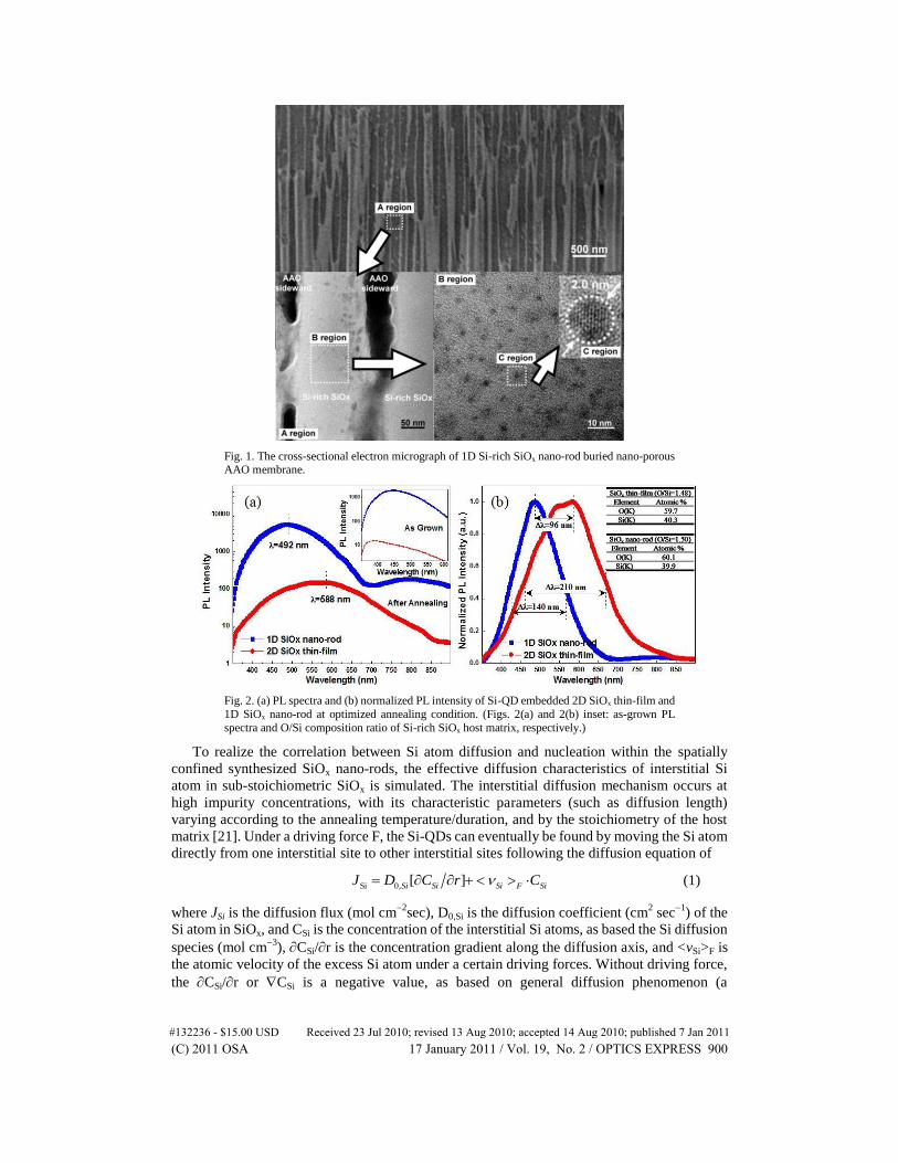
Fig. 1. The cross-sectional electron micrograph of 1D Si-rich SiOx nano-rod buried nano-porous AAO membrane.
Fig. 2. (a) PL spectra and (b) normalized PL intensity of Si-QD embedded 2D SiOx thin-film and
1D SiOx nano-rod at optimized annealing condition. (Figs. 2(a) and 2(b) inset: as-grown PL
spectra and O/Si composition ratio of Si-rich SiOx host matrix, respectively.)
To realize the correlation between Si atom diffusion and nucleation within the spatially
confined synthesized SiOx nano-rods, the effective diffusion characteristics of interstitial Si
atom in sub-stoichiometric SiOx is simulated. The interstitial diffusion mechanism occurs at
high impurity concentrations, with its characteristic parameters (such as diffusion length)
varying according to the annealing temperature/duration, and by the stoichiometry of the host
matrix [21]. Under a driving force F, the Si-QDs can eventually be found by moving the Si atom
directly from one interstitial site to other interstitial sites following the diffusion equation of
Si 0, [ ]Si Si Si F SiJ D C r C (1)
where JSi is the diffusion flux (mol cm2
sec), D0,Si is the diffusion coefficient (cm2 sec
1) of the
Si atom in SiOx, and CSi is the concentration of the interstitial Si atoms, as based the Si diffusion
species (mol cm3
), CSi/r is the concentration gradient along the diffusion axis, and <vSi>F is
the atomic velocity of the excess Si atom under a certain driving forces. Without driving force,
the CSi/r or CSi is a negative value, as based on general diffusion phenomenon (a
#132236 - $15.00 USD Received 23 Jul 2010; revised 13 Aug 2010; accepted 14 Aug 2010; published 7 Jan 2011(C) 2011 OSA 17 January 2011 / Vol. 19, No. 2 / OPTICS EXPRESS 900

spontaneous process initiated from high- to low-concentration region). Nevertheless, to obtain a
reverse diffusion flux, the D0,Si[CSi/r] + <νSi>F CSi must be smaller than zero. The definition
of driving forces [21], the diffusion equation can be rewritten as a function of Gibbs free energy
by J = D0,Si[CSi/r] + [CSiD0,SiΔGm/akT] under a driving force of ΔGm/a, where T and k are the
temperature and Boltzmann constant, respectively, ΔGm is the change of Gibbs free energy, and
the a is the distance between neighboring lattice planes. An increased ΔGm or decreased lattice
constant is necessary to inverse the atomic diffusion. According to the thermodynamic theory,
the change of Gibbs free energy could be related to ΔGm = ΔΗΤΔS, where ΔΗ and ΔS are the
enthalpy and the entropy, respectively. In our case, the negative diffusion flux caused by Si
atom nucleation from low-concentration to a high-concentration region, occurs by ΔH<0 and
ΔS>0 at a given annealing temperature, which can produce the ΔGm<0 condition and favor the
interstitial Si atom diffusion and nucleation.
On the other hand, the atomic diffusion theory has directly correlated the proportionality of
Si-QD radius to the SiOx composition ratio, the environmental temperature, and the duration of
heat treatment. According to Fick's first and second Laws, the diffusion length of 4 *D t with
D* = D0exp(Q/kT) is proportional to the square root of the time and diffusion coefficient [21],
which provides a confinement on the maximum movement of excessive Si atoms, within the
SiOx matrix, at a given annealing temperature and time. When the diffusion length is larger than
the bounded size, finite Si atoms can be aggregated to form the Si-QD of precisely controlled
size. For example, it takes nearly 624 Si atoms to form a Si-QD with a diameter of 2 nm in the
SiOx host matrix an O/Si composition of 1.5, which corresponds to the excess Si atom density of
2.82 × 10²⁰
cm3
. By using the excess density of a Si atom to estimate the spheral radius of the
formed Si-QD of 2 nm, we can obtain the spheral radius of 1.74 nm aggregate of Si-QD, and the
spheral radius is called the diffusion length. Theoretically, the diffusion length of 2.84 nm, as
determined using the above model [22], is larger than the above value. However, the diffusion
length determined by using either excess Si atom density or theoretical method do not larger
than the bounded size (nano-porous AAO membrane sideward), it is interesting to understand
other possible causes. According to the nucleation mechanism, Gibbs free energy is reduced
during Si-QD nucleation, while the grain boundary and defective position exhibit the lowest
nucleation energy to achieve the lowest Gibbs free energy. If the atoms are unable to diffuse to
the grain boundary, which will nucleate in the randomly distributed defective position within
the SiOx host matrix, then the Si-QD are enlarged, and eventually saturate at a size set by the
diffusion length of the excessive Si atoms within the SiOx matrix.
In comparison with an as-grown SiOx film, the SiOx nano-rod with buried Si-QD
as-deposited in a nano-porous AAO membrane shows defect related PL emissions at 415–455
nm of an intensity increasing over two orders of magnitude (see Fig. 2(a) inset). Such a
blue-green emission results mainly from the activation of dense radiative defects, such as weak
oxygen bonding or neutral oxygen vacancy (NOV) defects in the SiOx host matrix. According
to the fundamental theory of impurities in crystals [23], the interstitial atoms are vacancies
formed in pairs (called Frenkel defects). These vacancies induce interstitial atoms to randomly
form distributed defective positions within the SiOx host matrix. In other words, spatially
confined synthesis enhances defect density to promote more nucleated positions, which can
impede the route of diffusion and confine the degree of atomic aggregation. A schematic
illustration is presented in Fig. 3 to explain such a spatially confined synthesis of Si-QD in a
1-D SiOx nano-rod surrounded by a nano-porous AAO membrane. Annealing induced Si
atomic diffusion within a 1-D SiOx nano-rod is restricted by its defect density. However, when
annealing the SiOx film grown on Si substrate, the Si-QD can be aggregated by the excessive Si
atoms diffusing within the diffusion length. Therefore, the size of Si-QD buried in a 1D SiOx
nano-rod structure is smaller than that buried in 2D SiOx film on a smooth Si wafer.
Furthermore, the diffusion controlled growth mechanism is employed to determine the
activation energy of 6.284 kJ mole1
for Si atom diffusion, which also indicates that the
#132236 - $15.00 USD Received 23 Jul 2010; revised 13 Aug 2010; accepted 14 Aug 2010; published 7 Jan 2011(C) 2011 OSA 17 January 2011 / Vol. 19, No. 2 / OPTICS EXPRESS 901

decreasing O/Si composition ratio of SiOx host matrix reduce activation energy, and promote Si
atomic aggregation.
Fig. 3. A model of Si-QD aggregation according to which spatially confined synthesis of Si-QD
embedded in 1D SiOx nano-rod.
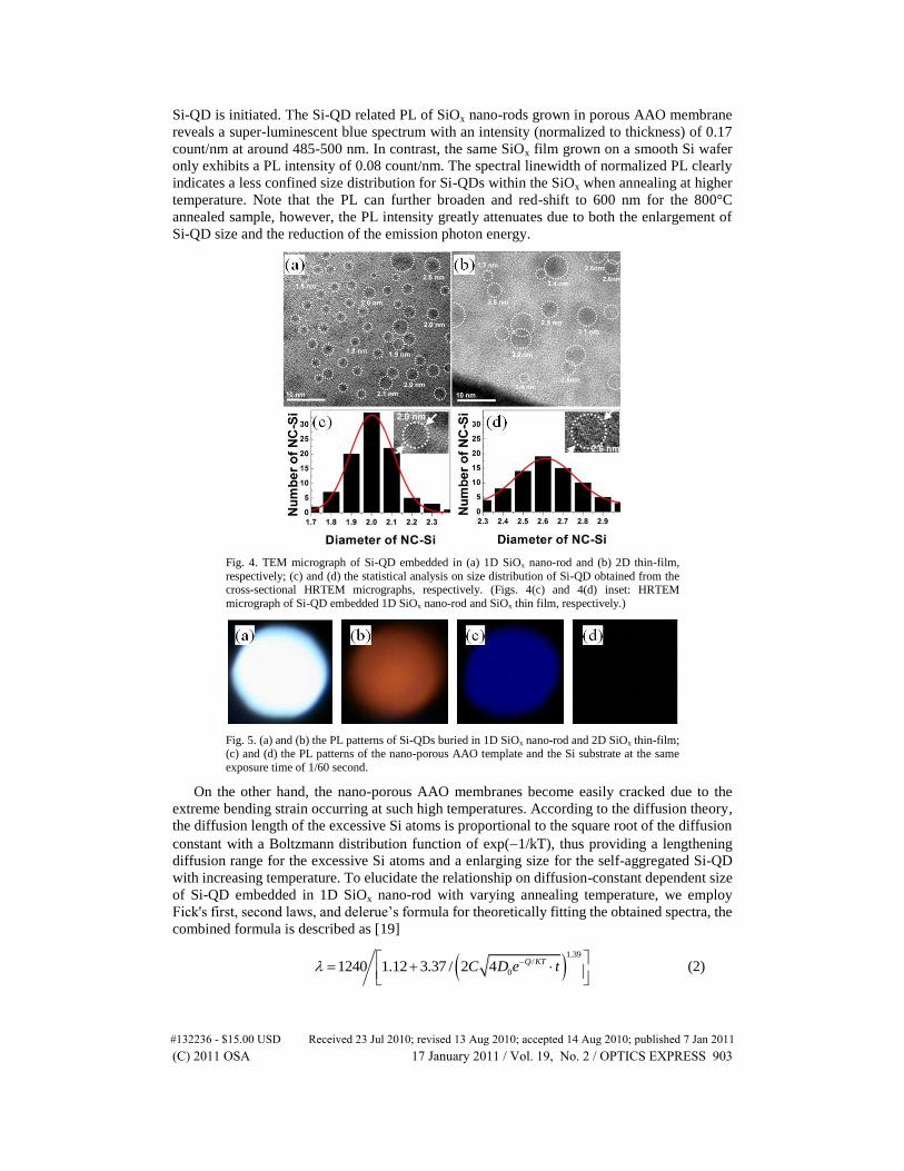
To further support the existence of Si-QD within the SiOx nano-rod deposited among
nano-porous AAO membrane with an O/Si composition ratio of 1.5, the high-resolution TEM
images are shown in Fig. 4. The average diameter and maximum volume density of Si-QD, with
a distinct lattice spacing of 0.31 nm, buried in SiOx thin-film are about 2.6 ± 0.2 nm and 5.71 ×
1017
cm3
, respectively. In comparison, the Si-QD within SiOx nano-rod buried in a
nano-porous AAO membrane shows tiny Si-QD with a smaller diameter of only 2.0 ± 0.1 nm,
but a higher volume density of 5.51 × 10¹⁸
cm3
(see Figs. 4(a) and 4(b)). The shrunken size and
enlarged volume density strongly correlates with the geometrically confined aggregation of
excessive Si atoms. Such a spatially confined effect also leads to a smaller standard deviation of
size, varied from 25% to 12.5% (Figs. 4(c) and 4(d)). By changing the host matrix of the
deposited SiOx from a smooth Si wafer to a nano-porous AAO membrane, the color of the PL
blue-shifts its central wavelength, decreasing from 588 nm to 492 nm to manifest the shrinking
size of Si-QD [21]. The spatial distribution of the Si-QDs is quantified by statistically analyzing
the distances between the nearest neighbors with a previously reported method [24]. Note that
the variance coefficient of Si-QDs should be as large as possible to reach uniform spatial
distribution in the host matrix. The distance variance of the distributed Si-QDs shown in Figs.
4(a) and 4(b) are 76% and 47%, respectively, indicating that the more uniform distribution of
Si-QDs inside AAO membrane is observed due to the numerous nucleation defects with
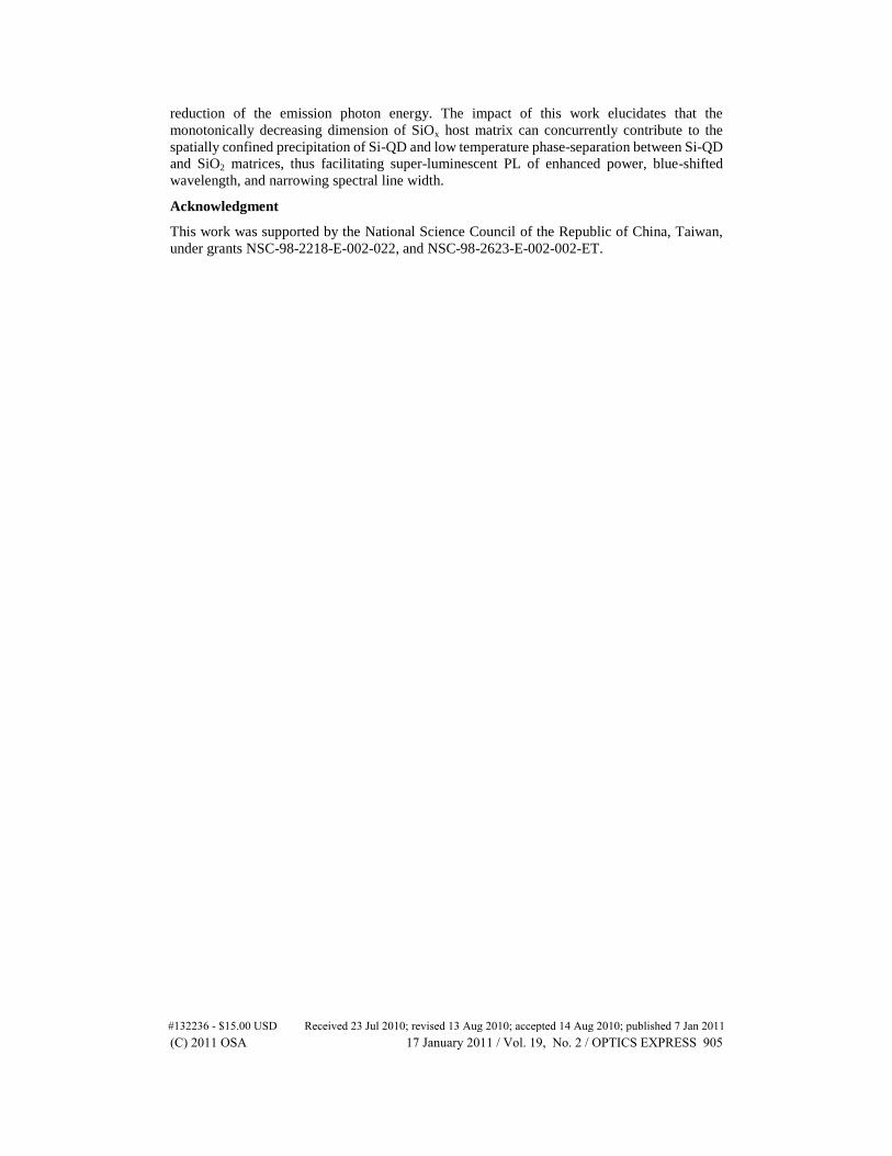
extremely low free-energy. A bright PL with white-light emitting pattern is contributed by the
Si-QDs precipitated within the spatially confined SiOx nano-rods deposited in nano-porous
AAO membrane. In contrast, the PL of Si-QDs self-aggregated in SiOx grown on Si wafer show
a dark-red-light (see Fig. 5). The smaller size of Si-QD buried in nano-rod structure eventually
leads to a higher volume density than that buried in the SiOx film. The emitting centers were
enhanced by increasing the volume density of Si-QD, which combines the enlarging bandgap
effect of Si-QD with decreasing size (d) to promote the PL intensity yield.
The PL of the SiOx nano-rod varied with annealing temperatures from 350 to 800°C, and
reveals a red-shifted and slightly broadened significant peak at the central wavelength as varied
from 450 to 600 nm, and shown in Fig. 6. When the annealing temperature is below 500°C, the
PL reveals a blue emission pattern as the Si-QDs within the SiOx are extremely small. The PL
intensity reached its maximum after annealing at 500°C as the precipitation of large-scale
#132236 - $15.00 USD Received 23 Jul 2010; revised 13 Aug 2010; accepted 14 Aug 2010; published 7 Jan 2011(C) 2011 OSA 17 January 2011 / Vol. 19, No. 2 / OPTICS EXPRESS 902
Si-QD is initiated. The Si-QD related PL of SiOx nano-rods grown in porous AAO membrane
reveals a super-luminescent blue spectrum with an intensity (normalized to thickness) of 0.17
count/nm at around 485-500 nm. In contrast, the same SiOx film grown on a smooth Si wafer
only exhibits a PL intensity of 0.08 count/nm. The spectral linewidth of normalized PL clearly
indicates a less confined size distribution for Si-QDs within the SiOx when annealing at higher
temperature. Note that the PL can further broaden and red-shift to 600 nm for the 800°C
annealed sample, however, the PL intensity greatly attenuates due to both the enlargement of
Si-QD size and the reduction of the emission photon energy.
Fig. 4. TEM micrograph of Si-QD embedded in (a) 1D SiOx nano-rod and (b) 2D thin-film,
respectively; (c) and (d) the statistical analysis on size distribution of Si-QD obtained from the cross-sectional HRTEM micrographs, respectively. (Figs. 4(c) and 4(d) inset: HRTEM
micrograph of Si-QD embedded 1D SiOx nano-rod and SiOx thin film, respectively.)
Fig. 5. (a) and (b) the PL patterns of Si-QDs buried in 1D SiOx nano-rod and 2D SiOx thin-film; (c) and (d) the PL patterns of the nano-porous AAO template and the Si substrate at the same
exposure time of 1/60 second.
On the other hand, the nano-porous AAO membranes become easily cracked due to the
extreme bending strain occurring at such high temperatures. According to the diffusion theory,
the diffusion length of the excessive Si atoms is proportional to the square root of the diffusion
constant with a Boltzmann distribution function of exp(1/kT), thus providing a lengthening
diffusion range for the excessive Si atoms and a enlarging size for the self-aggregated Si-QD
with increasing temperature. To elucidate the relationship on diffusion-constant dependent size
of Si-QD embedded in 1D SiOx nano-rod with varying annealing temperature, we employ
Fick's first, second laws, and delerue’s formula for theoretically fitting the obtained spectra, the
combined formula is described as [19]
1.39
/
01240 1.12 3.37 / 2 4 Q KTC D e t
(2)
#132236 - $15.00 USD Received 23 Jul 2010; revised 13 Aug 2010; accepted 14 Aug 2010; published 7 Jan 2011(C) 2011 OSA 17 January 2011 / Vol. 19, No. 2 / OPTICS EXPRESS 903

The simulation curve (blue line) using Eq. (2) for annealing temperature ranging from 350 to
800°C shown in Fig. 6 also indicates a good agreement with the experimental data. The
simulation clarifies that the diffusing constant eventually saturates at relatively high annealing
temperature, such that the Si-QD size can no longer expand to cause a red-shifted PL by
increasing temperature.
Fig. 6. The wavelength and linewidth of PL spectra as a function of annealing temperature (Inset:
Normalized PL intensity of Si-QD embedded SiOx nano-rod in nano-porous AAO membrane).
The observation of a PL signal from SiOx nano-rods in nano-porous AAO membrane, at
extremely low annealing temperatures, also corroborates that the Si-QD precipitation can be
initiated due to surface effects of a nano-scale structure, as compared to the bulk case [25]. Note
that many unusual thermodynamic behaviors are associated with spatial confinement synthesis.
Fitting the melting temperature of the semiconductor QDs by a phenomenological model
reveals a significant deviation with increasing size. Goldstein et al. indicated that the CdS
melting data agrees well with the phase equilibrium model [26], and the same model predicts a
rapid rise in Tm with the increasing particle size of the GaAs [27]. Such a low annealing
temperature is less than those reported in any previous work [16]. This phenomenon elucidates
that the monotonically decreasing dimension of the SiOx host matrix can concurrently
contribute to the spatially confined precipitation of Si-QD and low temperature
phase-separation between Si-QD and SiO2 matrices, thus facilitating super-luminescent PL
with enhanced power, blue-shifted wavelength, and narrowing spectral line width.
4. Conclusion
We have demonstrated the spatially confined synthesize of a SiOx nano-rod in nano-porous
AAO membrane, with ultra-bright PL after lower annealing temperature of 500°C. A higher
concentration, with a volume density of 5.51 × 10¹⁸
cm3
and a tiny size diameter of only 2.0 ±
0.1 nm, of the excessive Si-QD can be easily obtained. HRTEM results indicate that the
geometric form variations between 2D to 1D could also effectively reduce the standard
deviation of Si-QD size from 25% to 12.5%. The spatially confined synthesis greatly increases
the density of nucleated positions for Si-QD precursors, which essentially impedes the route of
thermally diffused Si atoms and confines the degree of atomic self-aggregation during
annealing. By using a diffusion controlled growth mechanism to estimate the diffusion
characteristics, we obtain the activation energy of 6.284 kJ mole1
with a diffusion length of
2.84 nm for a SiO1.5 nano-rod in nano-porous AAO membrane. These results also indicate that
the varied composition ratio of SiOx host matrix will affect the value of activation energy. In
contrast, the same SiOx film grown on smooth Si wafer only exhibits a PL intensity of 0.08
count/nm. The PL could further broaden and red-shift to 600 nm for the 800°C annealed sample,
however, the PL intensity greatly attenuates, due to both the enlarged Si-QD size and the
#132236 - $15.00 USD Received 23 Jul 2010; revised 13 Aug 2010; accepted 14 Aug 2010; published 7 Jan 2011(C) 2011 OSA 17 January 2011 / Vol. 19, No. 2 / OPTICS EXPRESS 904
reduction of the emission photon energy. The impact of this work elucidates that the
monotonically decreasing dimension of SiOx host matrix can concurrently contribute to the
spatially confined precipitation of Si-QD and low temperature phase-separation between Si-QD
and SiO2 matrices, thus facilitating super-luminescent PL of enhanced power, blue-shifted
wavelength, and narrowing spectral line width.
Acknowledgment
This work was supported by the National Science Council of the Republic of China, Taiwan,
under grants NSC-98-2218-E-002-022, and NSC-98-2623-E-002-002-ET.
#132236 - $15.00 USD Received 23 Jul 2010; revised 13 Aug 2010; accepted 14 Aug 2010; published 7 Jan 2011(C) 2011 OSA 17 January 2011 / Vol. 19, No. 2 / OPTICS EXPRESS 905