SPACE USER'S MANUAL
68
SPACE USER’S MANUAL N.P. van der Meijs, A.J. van Genderen, F. Beeftink, P.J.H. Elias Circuits and Systems Group Department of Electrical Engineering Delft University of Technology The Netherlands Report ET-NT 92.21 Copyright © 1992-2014 by the authors. All rights reserved. Last revision: Mar. 19, 2014.
-
Upload
khangminh22 -
Category
Documents
-
view
0 -
download
0
Transcript of SPACE USER'S MANUAL

SPACE USER’S MANUAL
N.P. van der Meijs,
A.J. van Genderen,
F. Beeftink,
P.J.H. Elias
Circuits and Systems Group
Department of Electrical Engineering
Delft University of Technology
The Netherlands
Report ET-NT 92.21
Copyright © 1992-2014 by the authors.
All rights reserved.
Last revision: Mar. 19, 2014.

Space User’s Manual 1
1. Introduction
1.1 What is Space
Space is an advanced layout to circuit extractor for analog and digital integrated circuits.
From a mask-level layout, space produces a circuit netlist. This netlist contains
• active devices,
• instances of other cells (only in hierarchical mode),
• terminals (if they are defined in the layout).
Optionally, this netlist contains
• wiring capacitances to substrate,
• inter-wire coupling capacitances (both cross-over coupling capacitances and lateral
coupling capacitances),
• wiring resistances,
• substrate resistances and capacitances.
These parasitics are extracted very accurately, this is a must for state-of-the-art IC
technologies where interconnection parasitics tend to determine maximum circuit
performance.
Besides accuracy, another key characteristic of space is efficiency. This is mainly due to
new algorithms for handling the IC geometry and careful implementation of the program.
Space is intended for on-line, interactive use but without problems it handles very large
designs even on a workstation or on a minicomputer.
Space can operate in hierarchical mode (in which case the extracted circuit possesses the
same hierarchical structure as the layout from which it is derived), in flat mode (in which
case only one circuit cell is generated for the total layout), or in mixed flat/hierarchical
mode.
1.2 Benefits of Using Space
A layout as extracted by space can be simulated while fully taking into account all
parasitic elements. This is important, since the decrease of feature sizes and the increase
of chip dimensions make the influence of wiring parasitics on the performance of the chip
critical, or even dominant: Gate delays decrease but wiring delays may actually increase.
Since space is an integrated on-line tool, and very fast, the effects of wiring parasitics can
be taken into account in the design loop . This prevents
The Nelsis IC Design System
Space User’s Manual 2
• missed performance targets or even malfunction of the silicon produced,
• and/or costly redesigns when the problem is detected late (when relying on stand-
alone verification tools).
Space enables meaningful performance/functional characterization, even for submicron
technologies, early in the design process.
1.3 Features
The main features of space are summarized as below. Space is ...
• hierarchical
• capable of extracting 45 degree polygonal layout
• extremely fast
The running time is linear in the size of the layout. The extraction speed is
depending on the extraction options selected.
• technology independent
Space is capable of extracting parasitics from analog and digital, MOS and bipolar
layouts. Space accepts user defined/adjusted element definition files.
• needs little computer memory
The memory usage is slightly worse than proportional to the square-root of the size
of the layout. Consequently, space can extract huge flat layouts using a minimum
amount of memory.
• accurately extracts lateral and crossover coupling capacitances
The capacitance model employed by space includes surface to surface, edge to
surface and edge to edge coupling capacitances.
• extracts bipolar device model parameters
Bipolar device model parameters are extracted using layout information like
emitter area, emitter perimeter and base width.
• employs Finite Element methods for accurate resistance extraction
These are much more accurate than polygon-partitioning based heuristics, and
nearly as efficient.
• produces accurate but simple RC networks
Space employs a new, Elmore time constant preserving algorithm to transform a
detailed Finite Element RC mesh into a low complexity lumped network that
accurately models the distributed nature of the parasitic resistance and capacitance
of IC interconnects. To model higher order time constants, the number of RC
sections in the output network is a function of the maximum signal frequency
which can be adjusted by the user.
The Nelsis IC Design System

Space User’s Manual 3
• can extract substrate resistances and capacitances
In order to model substrate coupling effects in analog and mixed digital/analog
circuits, space can apply an accurate numerical technique or a fast interpolation
technique to extract the substrate resistances. Additional, substrate capacitances
can be extracted using the same accurate technique or fast by using a rc-ratio.
• can read/write various layout/circuit formats
For example, CIF or GDSII input and SPICE, SPF, SPEF, EDIF or VHDL output.
• enables trading of accuracy versus computer time
Users can select the type of parasitics they want to extract.
1.4 Documentation on Space
The following documentation on space is available:
• Space User’s Manual
This document. It is not an introduction to space for novice users, those are
referred to the Space Tutorial .
• Space Tutorial / Space Tutorial Helios Version
The space tutorial provides a hands-on introduction to using space and the
auxiliary tools in the system that are used in conjunction with space. It contains
several examples. The space tutorial helios version provides a similar hands-on
introduction, but now from a point of view where the graphical user interface helios
is used to invoke space.
• Manual Pages
For space as well as for other tools that are used in conjunction with space, manual
pages are available describing (the usage of) these programs. The manual pages
are on-line available, as well as in printed form. The on-line information can be
obtained using the icdman program.
• Xspace User’s Manual
This short manual describes the usage of Xspace, a graphical X Windows based
interactive version of space. Note, however, that a more general graphical user
interface to space is provided by the program helios.
• Space 3D Capacitance Extraction User’s Manual
The space 3D capacitance extraction user’s manual provides information on how
space can be used to extract accurate 3D capacitances.
• Space Substrate Resistance Extraction User’s Manual
This manual describes how resistances between substrate terminals are computed
in order to model substrate coupling effects in analog and mixed digital/analog
circuits.
The Nelsis IC Design System

Space User’s Manual 4
2. Space Program Usage
2.1 Introduction
This chapter will describe space. Its many characteristic features are discussed in
separate sections within this chapter. Each of the features is controlled by one or more of
the following:
• Command-Line Options
These are mainly flags that can be used to enable or disable some aspects of the
extraction process or otherwise influence the behavior of space. For example,
capacitance extraction is disabled by default, but can be turned on by using the -c
option. Some options can also be specified in the parameter file. Options overrule
specifications in the parameter file.
• The Element Definition File
In this file, it is described how space can recognize the circuit elements (transistors,
contacts, interconnects etc.) from the layout. This file also contains unit values for
capacitances and resistances. By default, space reads this file from the appropriate
directory of the ICD process library. See also Section 2.11 and Chapter 3.
• The Parameter File
This file contains values for several variables that control the extraction process,
like minimum values of resistances to be retained in the extracted netlist. Also this
file is default read from the appropriate directory of the ICD process library. Some
parameters can also be specified as options. Options overrule specifications in the
parameter file. See also Section 2.12.
The relevant aspects of each of these control mechanisms are discussed in each section,
and are summarized at the end of each section. An overview of all command-line options
is given in appendix A.
2.2 General
2.2.1 Invocation and Basic Options
Space is normally invoked via the Unix command interpreter, or shell, as follows:
space [options] cellname [cellname ...]
The cellname arguments specify which layouts are to be extracted, at least one cellname
has to be specified. The options influence the behavior of space, as will be shown in the
rest of this chapter. A basic option is -v, which makes space prints some useful
information during the extraction process.
The Nelsis IC Design System

Space User’s Manual 5
2.2.2 Hierarchical and Flat Extraction
By default, space operates in hierarchical mode. In this mode, the circuit that is
produced has the same hierarchical structure as the layout from which it is derived.
Space will traverse the hierarchy itself, it is thus only necessary to specify the root(s) of
the tree(s) to be extracted on the command line. To forbit traversal use option -T. Note
that space does never extract imported sub-cells (cells of other projects).
Space operates in flat mode when using the -F option. In flat mode, the layout will be
fully instantiated (flattened) before extraction and the circuit will have no sub-cells
(except library and device cells, see xcontrol(1ICD)).
2.2.3 Mixed Flat/Hierarchical Extraction
In hierarchical mode, it is possible to perform a mixed flat/hierarchical extraction and by
defining one or more layout cells to have the macro status using xcontrol(1ICD).
In that case, in contrast to the instances of other cells, all instances of macro cells are
flattened before extraction. When a macro cell has one or more child cells itself, the
macro status of each of these child cells determines if the instances of these cells are also
flattened. The use of macros may for example be advantageous when using small sub-
cells for which it is cumbersome to define terminals (see Section 2.2.5), or when
extracting sea-of-gates circuits, where the image is in a separate cell that is instantiated
‘‘under’’ all other cells.
In flat mode, it is also possible to perform a mixed flat/hierarchical extraction. This can
be done by setting the library or device status for one or more sub-cells with xcontrol.
In that case, the layout of the whole circuit will be expanded, expect for the instances of
library and device cells, which will be included as instances in the extracted netlist.
2.2.4 Incremental Operation
In hierarchical mode, space operates in incremental mode by default. In incremental
mode, space does not extract sub-cells for which the circuit is up-to-date. Space uses an
internal algorithm to select cells for (re-)extraction, as follows:
• extract all cells that have not yet been extracted,
• extract all cells of which the layout is newer than the extracted circuit,
• extract all cells that have one or more child cells of which the layout is newer than
the extracted circuit,
• extract all cells that have one or more child cells for which the extraction status
(see xcontrol(1ICD)) has been changed after the last extraction of the cell,
• extract cells that are at a depth <= depth, where depth is specified with the option
-D depth. The root of the tree is at depth 1, its children are at depth 2, and so on.
By default, depth = 1, so cells that are are given as argument with space are always
extracted.
The Nelsis IC Design System

Space User’s Manual 6
Incremental mode is disabled completely with the -I option. In this non-incremental
mode, all cells in the tree are extracted. (Note that this option is equal to specifying a
large number for depth.) The options -I and -D are useful when changing extraction
style, e.g. to extract all cells with coupling capacitances if they were done with substrate
capacitances only.
2.2.5 Terminals
An electrical network or circuit as extracted by space, is built up from primitive elements
(transistors, capacitors and resistors), subcircuits (when the input layout is hierarchical)
and terminals. Terminals (sometimes also called ports or pins) are connectors to the
outside world and are used for building up the hierarchical structure of the circuit. The
extracted netlist specifies the connectivity among all these elements.
For space to be able to produce these terminals in the extracted circuit, the input layout
must also have terminals. Layout terminals are named rectangular areas or points (this is
dependent on how they are specified in the layout input file or using the layout editor) in
an interconnect layer of the layout. Space uses the terminals in the layout to create, name
and connect the terminals in the circuit according to a one-to-one correspondence
between layout terminals and circuit terminals. Terminal names must be unique within a
cell.
For flat extraction, only the topmost cell must have terminals. For hierarchical extraction,
the topmost cell and all the other cells in the hierarchy must have terminals, unless the
cell is used as a macro (see Section 2.2.3). Space identifies a connection from a cell
being extracted (the parent cell) to a sub-cell (or child cell) when a layout feature of the
parent cell touches or overlaps a terminal of the child cell. Space identifies a connection
between two sub-cells when a terminal of one sub-cell touches or overlaps a terminal of
another sub-cell.
NOTE:
If a sub-cell does not have terminals, set the macro status for the sub-cell, or use
flat extraction only.
In case of hierarchical extraction (without setting the macro status), space would not
detect such connections. In fact, space would be unable to represent those non-
hierarchical connections in a hierarchical circuit netlist. The program will not give a
warning in case of such non-hierarchical connections.
NOTE:
If a sub-cell has terminals but the sub-cell is connected via layout polygons of the
sub-cell that are only extensions the real terminal areas of the sub-cell, set the
interface type for the sub-cell to free (or freemasks) (using xcontrol(1ICD)) or use
flat extraction only.
By setting the interface type for the sub-cell to free (or freemasks), the layout of the sub-
cell will be expanded in the father cell (with freemasks only for certain masks) and the
The Nelsis IC Design System

Space User’s Manual 7
sub-cell will be appropriately connected via its terminals. Note, however, that other
elements may then also be recognized in the parent cell (see also Section 2.9).
2.2.6 Limitations of Hierarchical Extraction
Hierarchical extraction is also impossible (in the sense that it results in an incorrect
circuit) if the functionality of the child cells is modified by layout features in the parent
cells. For example, a polysilicon feature in a parent cell that overlaps an active area
feature in a child cell modifies the circuit of the child cell by creating a transistor in it.
Flat extraction is not a problem in this case and will result in a correct circuit.
While flat extraction is necessary in some cases as mentioned above, it is recommended
when it is required to get the highest accuracy of the parasitics extracted. One reason for
this is the fact that (parasitic) coupling capacitances between layout features of different
cells don’t fit in a hierarchical circuit description. However, flat extraction is often not a
significant burden because space is very fast. Also, the extracted circuit is often used for
simulation and most simulators must flatten the circuit anyway, since internally they only
can work on a flattened netlist.
Appendix B gives some guidelines for how to construct a layout such that a hierarchical
extraction by space will suffer least from these difficulties and hence is more accurate.
2.2.7 Command-Line Options
-v Set verbose mode.
-F Set flat extraction mode, i.e. produce a flattened netlist.
-T In hierarchical mode, only extract the top cell(s).
-I Unset incremental (hierarchical) mode: do not skip sub-cells
for which the circuit is up-to-date (depth = ∞).
-D depth Selectively unset incremental (hierarchical) mode for all cells
at level <= depth (default depth = 1).
-u Do not automatically run the preprocessors makeboxl(1ICD)
and makegln(1ICD).
2.2.8 Parameter File
When the parameter flat_extraction is specified in the parameter file, a flat extraction is
performed.
parameter type unit default suggestion
flat_extraction boolean - off -
The Nelsis IC Design System

Space User’s Manual 8
2.3 Extraction of Field-effect Transistors
Space recognizes field-effect transistors (e.g. MOS transistor) from the different mask
combinations in the layout (see Section 3.4). The extractor will calculate the width and
length of each field-effect transistor. For that matter, space uses perimeter and surface
formulas, as described below. When the -t option is used, the position of each transistor
is specified in the extraction output.
2.3.1 Drain-source connections
For each field-effect transistor space will extract one gate connection, optionally a bulk
connection, and one drain/source connection for each set of drain/source areas that are
connected. As an example, for the following layout of a transistor (which has 5
drain/source areas, divided into 2 different sets), space will extract one gate connection,
possibly a bulk connection (if this connection is specified in the element definition file),
one drain connection and one source connection.
If a field-effect transistor is used as a capacitor and has only one connected set of
drain/source areas, two connections will be generated that are however attached to the
same net. If a field-effect transistor has more than two drain/source connections, only
two of these connections appear in the extracted circuit. (These will in general be the
connections that are connected to other parts of the circuit; dangling connections are not
used in this case.)
2.3.2 Transistor width and length calculation
For each field-effect transistor, its width and length are calculated and stored in the
attributes w and l. The transistor width and length are calculated from
length =perg
Ng
width =A
length
where
The Nelsis IC Design System

Space User’s Manual 9
perg is the part of the perimeter of the transistor where the gate extends the active
area (see below),
Ng is the number of separate areas where this occurs, and
A is the total area of the transistor.
pertot = a + b + c + d + e + f
a
b
c d
e
fperg = a + d
If the transistor has no gate overlaps (Ng = 0) the width and length of the transistor are
calculated from:
width =pertot
2
length =A
width
where
pertot is the total perimeter of the transistor.
2.3.3 Transistor drain/source parameters calculation
When a condition list for the drain/source region of the transistor is specified in the
element definition file (see Section 3.4.9), and when capacitance extraction is enabled, the
area, perimeter and number of equivalent squares for both drain and source region will be
computed. In the perimeter of the drain and source, the edge that coincides with the
transistor channel, is not included. When more than one transistor is connected to a
drain/source region, the area value that is obtained for the total drain/source region is
subdivided over the different transistors in proportion to the widths of the transistors.
Apart from some constant that represents the length of the subdivided drain/source
regions, the perimeter value is split in a similar way. The number of equivalent squares
nrx for the drain/source region of a transistor is computed from:
nrx =ax
width2
where ax is the area of the drain/source region and width is the width of the transistor.
2.3.4 Command-Line Options
Extraction of field-effect transistors is controlled by the following option:
-t Add positions of devices and sub-cells to the extracted circuit.
The Nelsis IC Design System

Space User’s Manual 10
2.3.5 Element Definition File
See section 3.4.9 for the specification of the field-effect transistor elements.
2.4 Bipolar Device Extraction
Space recognizes bipolar junction transistors (BJT’s) by combining semiconductor
regions of type ’n’ and ’p’. Bipolar junction transistors are divided into two groups:
vertical and lateral transistors. For the vertical transistors, space calculates the emitter
area and perimeter. They are stored in the attributes area and length, respectively. For the
lateral transistors, the width of the base - the smallest distance between collector and
emitter - is also calculated and stored in the attribute basew. For both groups, the -t
option enables space to output the position of the emitter for each transistor.
2.4.1 Terminal connections
For each bipolar junction transistor, space will extract only one connection for each
device terminal (collector, base, emitter and optionally a substrate terminal). Multi-
emitter transistors are extracted as separate devices (one for each emitter). When a lateral
transistor is recognized that has the same mask for both the emitter and the collector
connections, it is assumed that the collector has the larger area.
2.4.2 Command-Line Options
Extraction of bipolar devices is controlled by the following option:
-t Add positions of devices and sub-cells to the extracted circuit.
2.4.3 Parameter File
The following parameters for the parameter file control the extraction of bipolar
transistors. The lat_base_width parameter defines the maximum base width that a lateral
transistor can have. Lateral transistor configurations with a width larger than this value
are not recognized as being transistors.
parameter type unit default suggestion
lat_base_width real micron 0 3
2.4.4 Element Definition File
See section 3.4.10 for the specification of the bipolar transistor elements.
2.5 Capacitance Extraction
2.5.1 Capacitance Definitions
Space uses an area/perimeter based capacitance extraction method. To describe the
capacitance model employed by space, refer to the following figure and definitions:
The Nelsis IC Design System
Space User’s Manual 11
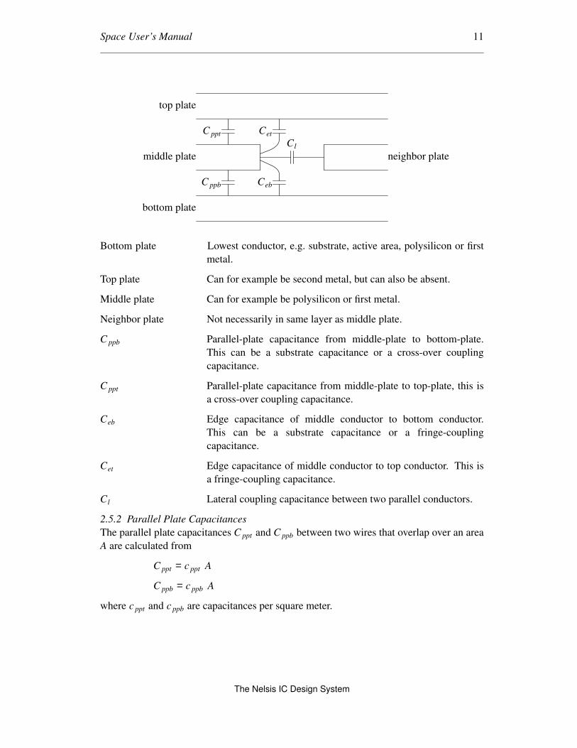
top plate
middle plate
bottom plate
neighbor plate
C ppb
C ppt
Cl
Ceb
Cet
Bottom plate Lowest conductor, e.g. substrate, active area, polysilicon or first
metal.
Top plate Can for example be second metal, but can also be absent.
Middle plate Can for example be polysilicon or first metal.
Neighbor plate Not necessarily in same layer as middle plate.
C ppb Parallel-plate capacitance from middle-plate to bottom-plate.
This can be a substrate capacitance or a cross-over coupling
capacitance.
C ppt Parallel-plate capacitance from middle-plate to top-plate, this is
a cross-over coupling capacitance.
Ceb Edge capacitance of middle conductor to bottom conductor.
This can be a substrate capacitance or a fringe-coupling
capacitance.
Cet Edge capacitance of middle conductor to top conductor. This is
a fringe-coupling capacitance.
Cl Lateral coupling capacitance between two parallel conductors.
2.5.2 Parallel Plate Capacitances
The parallel plate capacitances C ppt and C ppb between two wires that overlap over an area
A are calculated from
C ppt = c ppt A
C ppb = c ppb A
where c ppt and c ppb are capacitances per square meter.
The Nelsis IC Design System

Space User’s Manual 12
2.5.3 Lateral Coupling Capacitances
The value of a lateral coupling capacitance can be computed in two different ways,
dependent on how the capacitance is specified in the element definition file.
One possibility is that a single value for the capacitance is specified in the element
definition file. In that case, the lateral coupling capacitance between two parallel wires
that are at a distance d over a length l is calculated from
Cl = cl
l
d
where cl is the value that is specified in the element definition file (cl corresponds to the
capacitance for a configuration where the distance between both wires is equal to their
length).
Another possibility, which allows to specify more accurate capacitance values, is that the
the lateral coupling capacitance is specified as a function of different distances between
the wires. In that case, the specification of the lateral capacitance has one or more
(distance, capacitivity) pairs that each specify the capacitance between two parallel wires
of a length of 1 meter for one particular distance between the wires. The lateral coupling
capacitance for other configurations is found from an interpolation between two
(distance, capacitivity) pairs. For the interpolation, the function
Cl = la
d p
is used if the capacitance for both adjacent points is larger than zero and p ≥ 1, and
Cl = l (a
d+ b)
is used otherwise. If the actual distance is larger or smaller than any specified distance,
an extrapolation is done using the above functions.
Lateral coupling capacitance extraction is controlled by the lat_cap_window parameter
from the parameter file. This parameter specifies in microns the distance over which
lateral coupling capacitance is considered significant. When the wires are at a distance
that is larger than lat_cap_window, no lateral coupling capacitance will be extracted for
these wires.
2.5.4 Edge Capacitances
In addition to the edge-to-bottom capacitance Ceb and the edge-to-top capacitance Cet ,
also edge-to-edge capacitances between wires that are on top of each other can computed,
as Cee in the figure below.
The Nelsis IC Design System

Space User’s Manual 13
top plate
bottom plate
Cee
One possibility to specify edge capacitance in the element definition file is by specifying
a single value ce which denotes the edge capacitance per meter edge length. The edge
capacitance Ce between one wire that overlaps the edge of another wire over a length l, or
between two wires of which the edges coincide over a length l, is then calculated from
Ce = ce l
However, if also lateral coupling capacitances are extracted, these simple equations do
not hold anymore, as the values of Ceb, Cet and Cee are effected by the lateral
capacitances. Space offers two ways of dealing with this, either by using an heuristical
method, or by allowing the user to specify explicitly how large the edge capacitances
become if other conductors are nearby.
The heuristical method uses the fact that experiments show that for conductors that are
not too narrow and/or too close to other conductors, the sum of the ground capacitances
and the coupling capacitances that are connected to that conductor is approximately
constant. Therefore, for each conductor edge to which a lateral coupling capacitance is
connected, space tries to keep the sum of the ground capacitance and the coupling
capacitances constant by decreasing the value of the other (non-lateral) edge capacitances
that are connected to that edge. This is achieved by subtracting from each non-lateral
edge capacitance Cex (where Cex is Cet , Ceb or Cee) that is connected to the edge, a value
minimum Cex ,Cex Cl compensate_lat_part
Cex−all
, where Cex−all is the sum of all connected
non-lateral edge capacitances and compensate_lat_part is a parameter. Note that this
parameter has a default value 1 (for full compensation). But if you want to have no full
compensation, set the value of parameter compensate_lat_part smaller than 1.
The second way of dealing with the effect of lateral coupling on the edge capacitances, is
by explicitly specifying in the element definition file (distance, capacitivity) pairs, similar
to the possibility used for lateral coupling capacitances (see previous section). (Note, to
use this second way, parameter compensate_lat_part must be greater than 0.) Each pair
gives the edge capacitance per meter edge length for given distance to a neighboring
conductor that is of the same type (e.g. both wires are of type metal1). If (dmax, ce) is the
pair with maximal specified distance (and therefore also maximal edge capacitance),
Ce = ce l for all distances larger than dmax or for a situation where no neighboring wire of
the same type is present. The edge capacitance for other configurations is found from an
interpolation between two (distance, capacitivity) pairs. The following interpolation
The Nelsis IC Design System

Space User’s Manual 14
function is used:
Ce = ce (1 − b exp ( − p d) ) l
If the actual distance is smaller than any specified distance, the same formula is used,
with b fixed at 1. These formulas apply both for Ceb, Cet and Cee. Edge capacitances
that are explicitly specified as a function of the distance to neighbor wires, are not
affected by the first method.
2.5.5 Coupling Capacitances When Extracting Only Substrate/Ground Capacitances
When only substrate/ground capacitances are extracted and no coupling capacitances (the
option -c is used and the option -C and -l are not used), all non-lateral coupling
capacitances that are specified in the element definition file are added as ground
capacitances to the two wires to which the coupling capacitance is connected.
2.5.6 Extracting Capacitances of Different Types
For each capacitance that is extracted it is possible to specify its type (see Section 3.4.13).
Unlike parallel capacitances that are of a same type, parallel capacitances of a different
type are not joined during extraction.
2.5.7 Extracting Junction Capacitances
Default, junction capacitances (see Section 3.4.13) will be extracted as linear
capacitances.
If the parameter jun_caps is set to "non-linear" the extracted capacitance will be of the
specified type.
If the parameter jun_caps is set to "area" the extracted capacitance will be of the specified
type and, moreover, the value of the extracted capacitance will specify the area of the
element (if only an area capacitivity is specified for that capacitance type) or the edge
length of the element (if only edge capacitivity is specified for that capacitance type). If
jun_caps is set to "area", and both area capacitivity and edge capacitivity are specified for
one junction type, the value of the extracted capacitance will be equal to the extracted
capacitance value divided by the area capacitivity (so in this case, effectively, the total
vertical and horizontal junction area is extracted).
If the parameter jun_caps is set to "area-perimeter" the extracted capacitance will be of
the specified type and the area and perimeter of the element will be represented by the
instance parameters area and perim in the database. See section 4.2 for then how to
convert these parameter names to the parameter names that are appropriate for the
simulator that is used.
If the parameter jun_caps is set to "separate" the extracted capacitance will be of the
specified type and the area and perimeter of each capacitance that is specified in the
capacitance list for that type will separatedly be represented with parameters area<nr>
and perim<nr> where <nr> denotes that it is the <nr>-th. area or the <nr>-th. perimeter
element in the list. This may e.g. be useful when it is required that for one junction
The Nelsis IC Design System

Space User’s Manual 15
capacitance element the perimeter adjacent to the gate oxide and the perimeter adjacent to
the field oxide are specified as separate parameters. (See again section 4.2 for how to
convert the parameter names to the parameter names that are appropriate for the simulator
that is used.)
Note that junction capacitances of drain/source areas can also be extracted as drain/source
area and perimeter information attached to the MOS transistors, see Section 3.4.9.
2.5.8 Name of Ground or Substrate Node
Ground or substrate capacitances are on one side connected to a node that is called
"GND" (if @gnd is used as terminal mask in the element definition file) or "SUBSTR" (if
@sub is used as terminal mask in the element definition file), see Section 3.4.13. These
names can be changed using respectively the name_ground parameter and the
name_substrate parameter from the parameter file.
2.5.9 Command-Line Options
Capacitance extraction is controlled by the following options:
-c Extract capacitances to substrate/ground.
-C Extract coupling capacitances as well as capacitances to substrate.
This option implies -c.
-l Also extract lateral coupling capacitances, implies -C.
2.5.10 Parameter File
The following parameter for the parameter file controls the extraction of capacitances.
parameter type unit default suggestion
lat_cap_window real micron 0 3-5
compensate_lat_part real - 1 1
jun_caps string - linear area-perimeter
name_ground string - GND -
name_substrate string - SUBSTR -
2.5.11 Element Definition File
See section 3.4.13 for the specification of the unit capacitance values (i.e. c ppt , c ppb, cet ,
ceb and cl) for the different interconnection layers.
2.6 Resistance Extraction
2.6.1 General
When extracting resistances, space applies finite element techniques to construct a fine
resistance mesh that models resistive effects in detail. An example of a layout and the
finite element mesh produced for the polysilicon mask is in the figure below:
The Nelsis IC Design System

Space User’s Manual 16
The finite element mesh is equivalent to a detailed resistance network and space initially
constructs this detailed resistance network to model the resistances. Then it applies a
Gaussian elimination (or, equivalently, a star-triangle transformation) node reduction
technique to simplify the network and to find the final resistances. The final network will
in general contain (1) the nodes that are terminals, (2) the nodes that are labels, (3) the
nodes that are transistor connections (gate, source, drain, emitter etc.), (4) the nodes that
are introduced by the algorithm in Section 2.7, (5) the nodes that are connected to
resistances of different types, (6) - if metal resistances are not extracted or when equi-
potential lines are detected (see Section 2.8.1 and Section 2.8.11) - the nodes that
correspond to equi-potential regions, and (7) - if substrate resistances are extracted (see
the Space Substrate Resistance Extraction User’s Manual) - the nodes that represent
substrate terminals. This is described in more detail in Section 2.8.
When extracting resistances together with capacitances, the extractor will add lumped
capacitances to the nodes of the initial resistance network to model the distributed
capacitive effects. In that case, the node reduction will proceed such that the Elmore time
constants between the nodes in the final network are unchanged with respect to their
value in the fine RC mesh. This will guarantee that the electrical transfer function of the
final network closely matches that of the fine RC mesh and, consequently, that of the
actual circuit.
The extraction of resistances together with (ground) capacitances is illustrated below. In
(a) it is shown how a T shaped interconnection with terminals Ta, Tb and Tc is
subdivided into finite elements, which are all rectangles in this case. In (b) the RC
network is shown that models the resistive and capacitive effects in detail. In (c) the final
network is shown that is obtained after eliminating the internal nodes and collapsing the
nodes that belong to the same terminal.
The Nelsis IC Design System

Space User’s Manual 17
7.32 4.01
9.17
38.2 36.2
37.6
12
120.66
6
6
6 6
1.33
1.330.50.8
0.8
3 3
3
32
16
622 16
10 6
Tb
Tc
Ta
Tc2Tc1
Tb2
Tb1Ta1
Ta2
Tc
Ta Tb
(a)
(b)
(c)
2.6.2 Improved Accuracy
By default, space uses a rather coarse finite element mesh to compute resistances. The
accuracy of the resistances as obtained with this mesh may not always be sufficient. In
particular, obtuse triangles in the mesh may be generated that have a bad influence on the
accuracy of the method and that produce negative resistances in the detailed resistance
network. Under some circumstances, negative resistances (and negative capacitances as a
by-product of the network reduction heuristics) may also appear in the final network.
To obtain an improved accuracy with resistance extraction, the option -z, may be used.
On the penalty of a somewhat longer extraction time, this option generates a finer finite-
element mesh that contains (almost) no obtuse triangles. As a result, more accurate
resistance values are found and negative resistances do not occur in the output network.
When using the option -z, the parameter max_obtuse specifies the maximum (obtuse)
angle of a corner of a triangle of the finite element mesh. A smaller value for max_obtuse
(use 90 ≤ max_obtuse ≤ 180) results in a finer finite element mesh, but also in longer
extraction times.
The Nelsis IC Design System
Space User’s Manual 18
NOTE:
The usage of the option -z may result in large finite element meshes, and hence
long extraction times, when resistances are extracted for large rectangular areas like
e.g. wells.
2.6.3 Extracting Resistances of Different Types
For each conductor it is possible to specify the type of the resistance that is extracted (see
Section 3.4.8 and Section 3.4.12). Parallel resistances of different types will not be
joined during extraction. Neither will nodes be eliminated that are connected to
resistances of different types.
2.6.4 Selective Resistance Extraction
Selective resistance extraction is possible by specifying interconnects in a file called
’sel_con’ and by using either the option -k or -j. When using the option -k, resistances
will only be extracted for the interconnects that are specified in the file ’sel_con’. When
using the option -j, resistances will be extracted for all interconnects except for the
interconnects that are specified in the file ’sel_con’. The format of the file ’sel_con’ is as
follows. On each line, an x position, an y position and a maskname is specified. When
an interconnect has the specified mask on the specified layout position, that interconnect
is specified in the file.
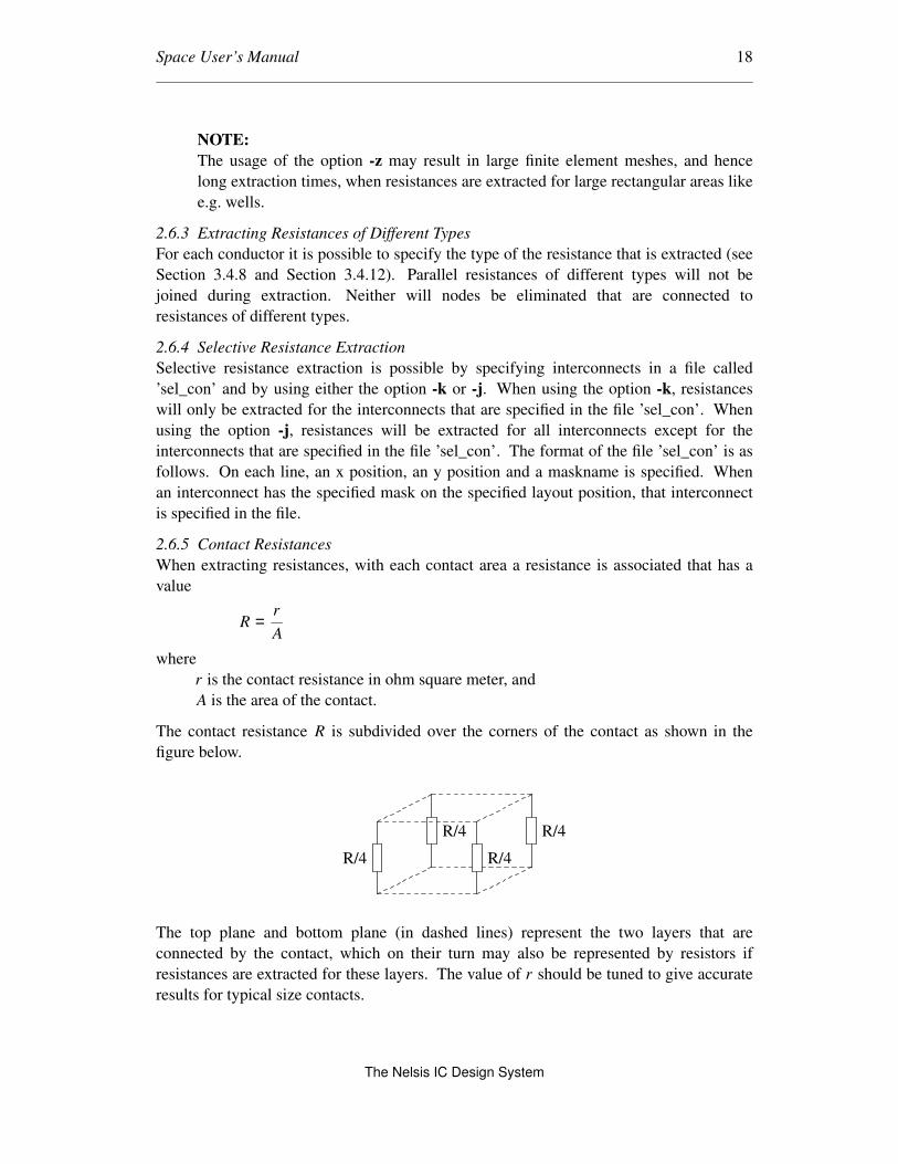
2.6.5 Contact Resistances
When extracting resistances, with each contact area a resistance is associated that has a
value
R =r
A
where
r is the contact resistance in ohm square meter, and
A is the area of the contact.
The contact resistance R is subdivided over the corners of the contact as shown in the
figure below.
R/4
R/4
R/4
R/4
The top plane and bottom plane (in dashed lines) represent the two layers that are
connected by the contact, which on their turn may also be represented by resistors if
resistances are extracted for these layers. The value of r should be tuned to give accurate
results for typical size contacts.
The Nelsis IC Design System

Space User’s Manual 19
2.6.6 Elimination Order
To reduce memory usage, space creates the detailed RC mesh while scanning the layout
from left to right. It eliminates each internal node as soon as this is possible, i.e. as soon
as all network elements that are connected to the node are known. However, this strategy
will in general result in an elimination order that is not optimal with respect to
computation time. Since the cost of each elimination is proportional to the square of the
number resistances that are connected to the node, it is often more efficient to first
eliminate the node that has the lowest number of resistances connected it, then the node
that has - after the previous operation - the lowest number of resistances connected to it,
etc.. To allow space to select for elimination a node with a low number resistances
connected to it, a buffer can be defined in which the nodes are temporarily stored that are
ready for elimination. When the buffer becomes full, the node with lowest degree is
selected for elimination and it is removed from the buffer. The size of the buffer is
defined using the parameter max_delayed. A large value of max_delayed may result in
significantly faster extraction times, but a too large value of max_delayed will also result
in large memory usage. A large value for max_delayed will in general be useful for
circuits that contain large rectangular area for which resistances are extracted such as n-
wells.
2.6.7 Command-Line Options
Resistance extraction is controlled by the following options:
-r Extract resistances for high-resistivity (non-metal) interconnect.
-z Apply mesh refinement for resistance extraction (implies -r).
-k Selective resistance extraction, resistances are only extracted for
specified interconnects.
-j Selective resistance extraction, resistances are extracted for all but
specified interconnects.
The threshold value to determine whether an interconnect is high-resistive or low-
resistive is specified by the parameter low_sheet_res in the parameter file (default,
low_sheet_res = 1 ohm per square).
2.6.8 Parameter File
Resistance extraction is controlled by the following parameters from the the parameter
file:
parameter type unit default suggestion
max_obtuse real degree 90.0 110.0
low_sheet_res real ohm 1.0 1.0
low_contact_res real ohm.m2 0.1e-12 0.1e-12
max_delayed integer - 100000 500-200000
The Nelsis IC Design System

Space User’s Manual 20
2.6.9 Element Definition File
See section 3.4.8 for the specification of the sheet resistance values for the
interconnection layers, and see section 3.4.12 for the specification of the contact
resistances.
2.7 Frequency Dependent Number of RC Sections
In some occasions (for high frequencies) the RC network that is extracted for the
interconnections may contain too few elements to allow a simulation of the extracted
circuit afterwards with sufficient accuracy. For example, if an interconnection has two
terminals, the extractor will extract an RC network consisting of one resistor and two
capacitors (one π -section), while an accurate simulation of the interconnection may
require at least two π -sections. In that case, the option -G may be used. This option
causes that, instead of eliminating all the internal nodes in the initial RC mesh (see
Section 2.6.1), a Selective Node Elimination (SNE) is performed in which, besides the
nodes that are normally retained in the extracted network (terminals, transistor
connections, etc; see Section 2.6.1), also other nodes are retained.
When using the the option -G, a parameter sne.frequency has to be specified in the
parameter file that specifies the maximum signal frequency that occurs in the extracted
circuit. The complexity of the extracted network will be a function of the parameter
sne.frequency. The higher the value of sne.frequency the more nodes will be retained in
the final network, such that the reduced network accurately models the detailed network
(i.e. the network before reduction). If sne.frequency ≤ 0, no additional nodes are retained.
As an example we consider the spiral resistor that is shown below.
The RC network that is default extracted for it is shown below in (a). When using the
option -G and when using for parameter sne.frequency the value 50e9, one non-terminal
node of the initial RC mesh will be retained in the final RC network and the RC network
as shown in (b) is obtained.
The Nelsis IC Design System

Space User’s Manual 21
57 fF
17.3 kΩ 10.0 kΩ 7.3 kΩ
(b)(a)
129 fF132 fF 74 fF 129 fF
2.7.1 Command-Line Options
More detailed RC network extraction is controlled by the following option:
-G Extract RC models that are accurate up to a certain frequency.
2.7.2 Parameter File
More detailed RC network extraction is controlled by the following parameter from the
the parameter file:
parameter type unit default suggestion
sne.frequency real Hz 1e9 1e9
2.8 Network Reduction Heuristics
When extracting resistances and capacitances, space can apply some heuristics to further
reduce the number of elements (resistors, capacitors and nodes) in the final network by
neglecting irrelevant detail. These heuristics include
• Retaining of nodes corresponding to equi-potential regions (i.e. pieces of
interconnect for which no resistance is extracted) in order to prevent the creation of
complete resistance graphs on the terminal nodes of large conductors (e.g. power
and ground lines, clock lines and large busses with many connections).
• Merging of (terminal) nodes that are connected by a small resistance.
• Removal of large resistances that are shunted by a low resistivity path.
• Reconnecting small coupling capacitances to ground.
Below, we will introduce these heuristics, and for illustration we use the following layout:
The Nelsis IC Design System

Space User’s Manual 22
metal metalpoly
e
d
c
b
a
In general, after Gaussian elimination but before applying the network reduction
heuristics, the network will contain (1) the nodes that are terminals, (2) the nodes that are
labels, (3) the nodes that are transistor connections (gate, source, drain, emitter etc.), (4)
the nodes that are introduced by the algorithm in Section 2.7, (5) the nodes that are
connected to resistances of different types, (6) - if metal resistances are not extracted or
when equi-potential lines are detected (see Section 2.8.1 and Section 2.8.11) - the nodes
that correspond to equi-potential regions, and (7) - if substrate resistances are extracted
(see the Space Substrate Resistance Extraction User’s Manual) - the nodes that represent
substrate terminals.
For the above example, when assuming that non-metal resistances and ground and
coupling capacitances are extracted, and when assuming that a, b, c, d and e are either
terminals or gate, drain or source connections, the network that is initially extracted will
have the following form:
m
e
d
c
b
a
C6
C5
C4
C3
C12
C2
C1 R5R4
R3
R2
R1
In the above figure, node m corresponds to the piece of metal that connects the three
different poly branches. If also metal resistances are extracted, or if no network reduction
heuristics are applied, this node will not be present.
The Nelsis IC Design System

Space User’s Manual 23
2.8.1 min_art_degree and min_degree heuristic
The articulation degree of a node is defined as the number of pieces in which the
resistance graph would break if the node and its connected resistances were removed.
Nodes that correspond to pieces of metal for which no resistances are extracted (e.g. node
m in the last figure) will often have an articulation degree > 1. If a node has an
articulation degree < min_art_degree and if (1) the node has no terminals or transistors
connected to it, (2) the node has not been introduced by the algorithm in Section 2.7, (3)
the node is not connected to resistances of different types, and (4) the node does not
represent a substrate terminal (see the Space Substrate Resistance Extraction User’s
Manual), the node will be eliminated. If an equi-potential node has an articulation degree
>= min_art_degree, or if it does not satisfy one of the 4 above conditions, the node will
be retained in the final network.
The degree of a node is equal to the number of resistances connected to the node. Nodes
with a degree >= min_degree and an articulation degree > 1 will also be retained in the
final network.
Example:
Node m is not eliminated if its articulation degree (3 in this case) is more than or
equal to min_art_degree, or if its articulation degree is more than one and its
degree (4 in this case) is more than or equal to min_degree. Otherwise, the node is
eliminated.
N.B. To find the articulation degree of a node, the extractor does not take into account
interconnection loops.
2.8.2 min_res heuristic
This heuristic deletes small resistances from the network via Gaussian elimination of one
of the nodes that is connected to the resistance. If a resistor has an absolute value that is
less than the min_res parameter, and if the resistor is connected to a node that (1) is not
connected to resistances of different types, and (2) does not have an articulation degree
>= min_art_degree, or a degree >= min_degree (see the previous paragraph), the
resistance is deleted by the elimination of that node. Terminals and transistor connections
of the node that is eliminated are added to the other node that is connected to the resistor.
The deletion is done incrementally: each time when one or more node have been
eliminated, the network is checked again to see if new small resistances have arisen.
Example:
The resistors R1, R2, R3, R4 and R5 are evaluated to see if their value is less than
min_res. If this is true then one of the nodes to which the resistor is connected to is
eliminated (not node m if this node was retained because of its degree or
articulation degree) and its terminal label(s) and/or transistor connections are
attached to the other node. The new network is again verified to see if there are any
resistors that are smaller than min_res, etc.
The Nelsis IC Design System

Space User’s Manual 24
2.8.3 min_sep_res heuristic
This heuristic deletes small resistances from the network by joining the two nodes that
are connected by the resistance. If two nodes are connected by a resistor that has an
absolute value that is less than min_sep_res, the resistor is deleted and the two nodes are
merged. Note that while the min_res heuristic does not affect the total resistance between
the remaining nodes, this heuristic, in general, does.
2.8.4 max_par_res heuristic
This heuristic prevents the occurrence of high-ohmic shunt paths between two nodes. If
the ratio of the absolute value of a resistor and its minimum parallel resistance path
(along positive resistors) exceeds the value of the max_par_res parameter, then the
resistor is simply removed.
Example:
Assume R3 > 0, R4 > 0 and R5 > 0. First it is checked if R3 / (R4 + R5) >
max_par_res. If this is true then R3 will be removed. If this is not true then it is
checked if R4 / (R3 + R5) > max_par_res. If this is true then R4 will be removed.
If this is not true then it is checked if R5 / (R3 + R4) > max_par_res. If this is true
then R5 will be removed. Recall that the elimination order is arbitrary.
2.8.5 no_neg_res heuristic
If the no_neg_res heuristic is on, all negative resistances will be removed from the
network.
2.8.6 min_coup_cap heuristic
If, for both nodes a coupling capacitance is connected to, it holds that the ratio between
the absolute value of the coupling capacitance and the value of the ground/substrate
capacitance of the same type of that node, is less than the min_coup_cap parameter, then
the value of the coupling capacitance is added to the ground capacitances of the two
nodes and the coupling capacitance is removed.
Example:
If C12 / C1 < min_coup_cap and C12 / C2 < min_coup_cap then C12 is removed and
its value is added to both C1 and C2.
2.8.7 min_ground_cap heuristic
If the absolute value of a ground/substrate capacitance is less than the min_ground_cap
parameter, the ground/substrate capacitance is removed.
2.8.8 no_neg_cap heuristic
If the no_neg_cap heuristic is on, all negative capacitances will be removed from the
network.
2.8.9 frag_coup_cap heuristic
In contrast to the other heuristics, this heuristic is applied during Gaussian elimination
(see Section 2.6.1). When eliminating a node and redistributing a coupling capacitance
that is connected to that node over the nodes that are adjacent, this heuristic decides
The Nelsis IC Design System

Space User’s Manual 25
whether or not the adjacent node receives (a part of) the coupling capacitance. When
Rmin is the minimum of the absolute values of the resistances that are connected to the
node that is eliminated, and when R is the value of the resistance between the node that is
eliminated and an adjacent node, then the adjacent node receives (a part of) the coupling
capacitance if and only if Rmin / |R| ≥ frag_coup_cap. Hence, a lower value of
frag_coup_cap will give more detail in the extracted network, but it will also result in
longer extraction times. For the fastest and least accurate form of resistance and coupling
capacitance extraction, set frag_coup_cap equal to 1.
2.8.10 min_coup_area, min_ground_area and frag_coup_area heuristics
These heuristics are similar to their equivalences for capacitance (min_coup_cap,
min_ground_cap and frag_coup_cap), but are used instead when junction capacitances
are extracted as area and perimeter elements (see Section 2.5.7). They only look at the
value of the area parameter(s) of the elements, not at the value of the perimeter
parameter(s).
2.8.11 equi_line_ratio heuristic
If, during resistance extraction, for a rectangular piece of interconnect, the ratio
length/width is more than equi_line_ratio, an equi-potential line is generated for that
piece of interconnect. The equi-potential line is placed at the middle of the rectangle,
perpendicular to the current flow. This will introduce an extra equi-potential node that is
treated similarly as the nodes that are introduced by not extracting metal resistances (see
Section 2.8.1). In general, this will simplify the extracted network and reduce extraction
time. Especially when metal resistances are extracted, the reduction in network
complexity and extraction time can be large. Currently, equi-potential lines are not
detected for all interconnect rectangles.
2.8.12 keep_nodes
It is possible to keep nodes of certain capacitance (and contact) elements in the extracted
network (these nodes are not eliminated). You need to specify a string of element names
after the keep_nodes parameter. When you only want to keep one of the nodes of an
element, you must add ’.1’ or ’.2’ to the element name. See for element names and the
pin order the technology file.
Example:
keep_nodes lcap_cms ecap_cms_cpg.2
The Nelsis IC Design System
Space User’s Manual 26
2.8.13 Parameter File
The heuristics are controlled by the following parameters from the parameter file:
parameter type unit default suggestion
min_art_degree integer — +∞ 3
min_degree integer — +∞ 4
min_res real ohm 0 100
min_sep_res real ohm 0 10
max_par_res real — +∞ 25
no_neg_res boolean — off on
min_coup_cap real — −∞ 0.04
min_ground_cap real farad 0 1e-15
no_neg_cap boolean — off on
frag_coup_cap real — 0 0.2
min_coup_area real — −∞ 0.04
min_ground_area real farad 0 1e-11
frag_coup_area real — 0 0.2
equi_line_ratio real — +∞ 1.0
keep_nodes string — — —
2.8.14 Command-Line Options
The following command-line option controls the heuristics:
-n Do not apply the circuit reduction heuristics.
2.9 Library Cell Circuit Extraction
When extracting a circuit that contains library cells (standard cells, gate arrays) the
library cells themselves often need not to be extracted, but only the interconnects between
the library cells. To let space perform an extraction in this way, set the extraction status
for each library cell to "library" using the program xcontrol(1ICD). When a cell has a
library status, space will not extract this cell, but it will include it as an instance in the
extracted circuit, no matter whether hierarchical extraction is used or flat extraction.
The description of the library cell itself can be added to the database using a netlist
conversion tool like cspice(1ICD) or csls(1ICD). When, however, instead of a netlist
description, a model description needs to be specified for the library cell, set the
extraction status for that cell to "device" using xcontrol(1ICD) and specify the model in
the control file of the netlist retrieving tool (see Section 4) or use the tool
putdevmod(1ICD) to specify the device model.
Sometimes it may be necessary to expand (parts of) the library cell in the parent cell.
This may for example be the case when the cell connects to the father cell via other
layout polygons than its terminal areas, or when the cell has feed-throughs that occur via
The Nelsis IC Design System

Space User’s Manual 27
other layout polygons than its terminal areas. In that case, set the interface type for the
cell to free (or freemasks) using the command xcontrol(1ICD). This way, the contents of
a library cell (for freemasks only certain masks) will be expanded its parent cell. Note,
however, that capacitances etc. inside the cell will then also be extracted. If this is not
desired (because the capacitances have already been accounted for in the description that
is available for the library cell), one can use the following strategy: Add a dummy mask
to the library cell and modify the element definition file that is used for extraction such
that capacitances are only recognized for positions where the dummy mask is not present.
To prevent the replication of data, it is useful to store the library cells in a separate project
and next import this project in the project where the design is present.
2.10 Back Annotation
2.10.1 Instance names
An instance name for a layout cell can be specified using a layout import tool (e.g. cgi)
or using the layout editor dali. The corresponding instance in the extracted circuit will
have the same name. If an instance in an extracted circuit is obtained from more than one
level down in the hierarchy of that cell (e.g. in case the instances that contain the relevant
instance are expanded in the top-level cell), the name of that instance is obtained by
concatenating the names of all the different instances that contain the instance. The
different instance names in this case are separated by a character that is specified by the
parameter hier_name_sep (default the character ’.’). If no instance name is specified in
the layout, or if a hierarchical instance name can not be constructed because one of the
instance names is missing, the instance name in the extracted circuit will be generated by
the network retrieving tool that is used.
The instance names of elements that are recognized from the mask layout combinations
(transistors, resistors, capacitors etc.) are generated by the extraction program or by the
network retrieving tool that is used.
2.10.2 Net names
A net in the extracted circuit represents one conductor or (defined from a layout point of
view) one set of electrically connected polygons. If no resistances are extracted, a net is
represented in the circuit by exactly one node. If resistances are extracted, a net may be
represented in the circuit by more than one node.
The name of a net, among other things, may be used to determine the names of the nodes
that are part of the net (see Section 2.10.4). The specification of a net name can be done
as follows:
• By defining a label for the net. The definition of a label requires the specification of a
name, a mask, an x, y position and (optionally) a class. The name of the label is then
used as the name for the net that is represented by the specified mask at the specified
position. If more than one label is attached to a net, the net receives the name of the
The Nelsis IC Design System

Space User’s Manual 28
label that has the smallest x coordinate or (if both x coordinates are equal) the
smallest y coordinate. Labels may be defined as follows:
— Using the layout editor dali in the annotate menu.
— Using the program cgi.
If the parameter no_labels is set, the labels that are defined for a cell will not be used
by the extractor.
• By setting the parameter term_is_netname. This will cause that each terminal of the
cell (hence, not a terminal of a sub-cell !) is also interpreted as a label. Again, if more
than one label is attached to a net, the net receives the name of the terminal that has
the smallest x coordinate or (if both x coordinates are equal) the smallest y
coordinate.
• By the use of inherited labels. Inherited labels originate from labels and terminals
that are defined in sub-cells:
If the parameter hier_labels is set, a label will be inherited from each label of a sub-
cell that is flattened in the extracted cell.
If the parameter hier_terminals is set, a label will be inherited from each terminal of a
sub-cell that is flattened in the extracted cell.
If the parameter leaf_terminals is set, a label will be inherited from each terminal of a
sub-cell that is not flattened in the extracted cell.
In each of the three above cases, the name of the inherited label is given by
concatenating the names of all the different instances that contain the original label or
terminal plus the name of the label or terminal itself. The different instance names
are separated by a character that is specified by the parameter hier_name_sep (default
the character ’.’). The instance name(s) and the label or terminal name are separated
by a character that is specified by the parameter inst_term_sep (default the character
’.’). If not all instance names are defined for the inherited label, or if the parameter
cell_pos_name is set, the name will be based on the name of the cell that the original
label or terminal comes from, the original label or terminal name and the position of
the inherited label.
The name of an inherited label is used to name the net that is connected to it only if
this net has not a normal label connected to it. For the rest, inherited labels are used
in the same way as normal labels.
2.10.3 Nodes
A node represents a vertex in the circuit graph. If no resistances are extracted, exactly
one node will be created for a net. If resistances are extracted (see Section 2.6), more
than one node may be created for a net.
The Nelsis IC Design System
Space User’s Manual 29
2.10.4 Node names
Default, nodes in the circuit are assigned a name that is an integer number. Howev er, the
latter is overruled in the following ways:
• A node in the circuit that represents a terminal of the cell receives a name that is equal
to the terminal name.
• A node in the circuit that represents a (inherited) label of the cell receives a name that
is equal to the label name.
• If resistances are extracted, if the node belongs to a net that has a name (see Section
2.10.2) and if the node does not represent a terminal nor a label, then the node has a
name <netname><separator><number>, where <netname> is the net name,
<separator> is specified using the parameter net_node_sep (default it is the character
’_’) and <number> is an integer number.
• If the parameter node_pos_name is set, each node has a name
<prefix><mask>_<xpos>_<ypos>, where <prefix> is a prefix that is specified using
the parameter pos_name_prefix (default it is an empty string), and the tuple <mask>,
<xpos> and <ypos> denotes a part of the layout (mask, x coordinate and y coordinate)
that corresponds to the node. It is the point that has the smallest x value and, next, the
smallest y value.
Note that it is possible that a node in the output netlist has more than one name, also
because during resistance extraction different nodes may be joined. Depending on the
netlist format that is used, not all names may be part of the output netlist.
2.10.5 Positions of devices and sub-cells
When the option -t is used with space or when the parameter component_coordinates is
set, positions of devices and sub-cells are added to the extracted circuit.
2.10.6 Name length
The maximum number of characters in an instance, node or net name is determined by
the project version number. The project version number is given on the first line of the
.dmrc file and for e.g. version number 3 the maximum name length is 14, for version
number 301 the maximum name length is 32 and for version number 302 the maximum
name length is 255. The mkpr program creates only projects for version number 302.
Node or net names that are generated by space and that are longer than the maximum
name length allowed by the project version number, are converted to a shorter name. A
translation table cell.nmp will then give the mapping between the original names and the
new names. The maximum name length can be decreased (e.g. because the simulator that
is used after the extraction can not handle the long names) by specifying a new maximum
length using the parameter max_name_length
When a long name is converted to a short name, the parameter trunc_name_prefix
specifies a prefix string for the new name (default is "n").
The Nelsis IC Design System

Space User’s Manual 30
2.10.7 More back-annotation information
The use of the option -x or setting the parameter backannotation causes that space will
also generate layout back-annotation information about the geometry of the different nets,
the different transistors etc. This information can e.g. be used as input for the program
highlay. The option -x or the parameter backannotation implies the option -t.
2.10.8 Parameter File
Back annotation is controlled by the following parameters from the parameter file:
parameter type default
hier_name_sep char .
inst_term_sep char .
no_labels boolean off
hier_labels boolean off
hier_terminals boolean off
leaf_terminals boolean off
cell_pos_name boolean off
term_is_netname boolean off
net_node_sep char _
node_pos_name boolean off
pos_name_prefix string <empty>
max_name_length int 32
trunc_name_prefix string n
component_coordinates boolean off
backannotation boolean off
2.10.9 Command-Line Options
The following command-line options control back-annotation:
-t Add positions of devices and sub-cells to the extracted circuit.
-x Generate layout back-annotation information, implies -t.
2.11 Element Definition Files
Space is technology independent. At start up, it reads a tabular element definition file
specifying how the different elements like conductors and transistors can be recognized
from the different mask combinations, and which values should be used for for example
conductor capacitivity and conductor resistivity. This tabular element file is constructed
from a user-defined element definition file by the space technology compiler tecc.
The default element definition file is space.def.t in the appropriate directory of the ICD
process library. Howev er, there can be several other element definition files for a
particular process. For example, the file space.max.t may contain an element description
with worst-case capacitance and resistance values. If this file exists, it can be read rather
The Nelsis IC Design System

Space User’s Manual 31
than the standard file by specifying -e max at the command line.
The user can also prepare his own element definition file and specify the name of that file
with the -E option. For a description of how to prepare an element definition file, see
Chapter 3. But usually it is most convenient to modify a copy of the source of one of the
‘‘official’’ element definition tables. These sources are also in the ICD process library.
2.11.1 Command-Line Options
The command line options are as follows:
-e xxx Use the file space.xxx.t in the ICD process library as the element
definition file.
-E file Use file as the element definition file.
2.12 Parameter Files
The parameter file for space contains values for several variables that control the
extraction process. For example, it contains all parameters that control the network
reduction heuristics.
The default parameter file is space.def.p in the appropriate directory of the ICD process
library. Howev er, an alternative parameter file in the ICD process library can be used by
using the -p option at the command line, and other files can be used by specifying the -P
option at the command line.
Parameters can be of different types, e.g. real, integer, string and boolean. If a parameter
is of type boolean, its value can be either on or off. If the name of a boolean parameter is
included in the parameter file, but no value is specified, this is equivalent to specifying the
value on.
Some parameters have a name class.parameter (e.g. sne.frequency). In this case, a group
of parameters of the same class may be used without the prefix "class." if they are
included between the lines "BEGIN class" and "END class". E.g.
BEGIN sne
frequency 1e9
END sne
is equivalent to
sne.frequency 1e9
The value of a parameter in the parameter file can also be specified using the option -S
param=value. This sets parameter param to the value value and overrides the setting in
the parameter file. (-S param is equivalent to -S param=on.)
Some parameters can also be specified as options, e.g. the use of the option -F is
equivalent to specifying the parameter flat_extraction in the parameter file. Options
The Nelsis IC Design System

Space User’s Manual 32
overrule specifications in the parameter file and specifications using the option -S
param=value.
2.12.1 Command-Line Options
The command line options are as follows:
-p xxx Use the file space.xxx.p in the ICD process library as the parameter
file.
-P file Use file as the parameter file.
-S param=value Set parameter param to the value value, overrides the setting in the
parameter (.p) file. (-S param is equivalent to -S param=on.)
The Nelsis IC Design System

Space User’s Manual 33
3. Developing Space Element Definition Files
3.1 Introduction
The element definition file describes how space recognizes the circuit elements
(transistors, contacts, interconnection layers etc.) from the layout definition of the cell.
The element definition file further contains the values for the different interconnect
capacitances, the sheet resistances for the interconnect layers, etc.
The program tecc acts as a pre-processor for technology descriptions for the space layout
to circuit extractor. From a user-defined element-definition source file, tecc produces a
compiled element-definition file that can be used as input for space.
3.2 Invocation and Command Line Options
The program tecc is invoked as follows:
tecc [-sn] [-m maskdatafile] [-p process] file
The user-defined input file should have the extension ’.s’, while the compiled output file
will have the same name but with ’.t’ substituted for ’.s’. The compiled output file is an
ascii file, hence it can easily be exchanged between different types of machines.
3.2.1 Command-Line Options
The following options can be specified:
-s Silent mode. This will suppress some diagnostics information, see
section 3.5.
-n Do not compress table-format element-definition file. This option is
useful during element-definition file development. It makes tecc run
faster, and space somewhat slower.
-m maskdatafile
Specifies the maskdatafile. Default, the maskdatafile is obtained from
the process directory.
-p process
Specifies the process. The default process is determined by the
current project directory. This option allows to run tecc outside a
project directory.
The Nelsis IC Design System

Space User’s Manual 34
3.3 Example Technology
In this section, we will use a double metal Nwell CMOS process as an example. This
technology is known in the system under the name ’scmos_n’, and the technology files
can be inspected. The masks that are used are the following:
maskname description/purpose
cpg polysilicon interconnect
caa active area
cmf metal interconnect
cms metal2 interconnect
cca contact metal to diffusion
ccp contact metal to poly
cva contact metal to metal2
cwn n-well
csn n-channel implant
cog contact to bondpads
The process is similar to the Mosis n-well scmos process. An element definition file for
this process is included as appendix D, and a parameter file as appendix E.
For illustrating the features that are only meaningful to bipolar processes, we will use the
bipolar DIMES-01 process as example. An element definition file for this process is
included as appendix F. The standard masks of this process are:
maskname description/purpose
bn buried N-layer
dp deep P-well; island isolation
dn deep N-well; collectorplug of all NPNs
wp extrinsic base of the NPNs
bw intrinsic base of the BW-NPN
wn shallow N-layer; washed emitter implantation
co contact windows in wp, sn and sp
ic interconnect layer
ct second contact window for in-ic contact
in second interconnect layer
3.4 The Element Definition File
3.4.1 General
The element-definition file defines the circuit elements that can be recognized from the
layout description. For each of the elements, at least a name and a condition list have to
be specified. In this subsection, names and condition lists are defined. They are
illustrated in the next subsections.
The Nelsis IC Design System
Space User’s Manual 35
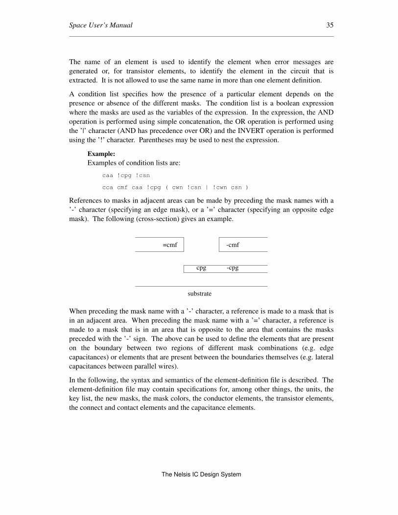
The name of an element is used to identify the element when error messages are
generated or, for transistor elements, to identify the element in the circuit that is
extracted. It is not allowed to use the same name in more than one element definition.
A condition list specifies how the presence of a particular element depends on the
presence or absence of the different masks. The condition list is a boolean expression
where the masks are used as the variables of the expression. In the expression, the AND
operation is performed using simple concatenation, the OR operation is performed using
the ’|’ character (AND has precedence over OR) and the INVERT operation is performed
using the ’!’ character. Parentheses may be used to nest the expression.
Example:
Examples of condition lists are:
caa !cpg !csn
cca cmf caa !cpg ( cwn !csn | !cwn csn )
References to masks in adjacent areas can be made by preceding the mask names with a
’-’ character (specifying an edge mask), or a ’=’ character (specifying an opposite edge
mask). The following (cross-section) gives an example.
cpg -cpg
-cmf=cmf
substrate
When preceding the mask name with a ’-’ character, a reference is made to a mask that is
in an adjacent area. When preceding the mask name with a ’=’ character, a reference is
made to a mask that is in an area that is opposite to the area that contains the masks
preceded with the ’-’ sign. The above can be used to define the elements that are present
on the boundary between two regions of different mask combinations (e.g. edge
capacitances) or elements that are present between the boundaries themselves (e.g. lateral
capacitances between parallel wires).
In the following, the syntax and semantics of the element-definition file is described. The
element-definition file may contain specifications for, among other things, the units, the
key list, the new masks, the mask colors, the conductor elements, the transistor elements,
the connect and contact elements and the capacitance elements.
The Nelsis IC Design System

Space User’s Manual 36
NOTE:
Each of the specifications in Sections 3.4.3-3.4.13 is optional but their order is
fixed.
3.4.2 Comment
Comments can be included in the element-definition file by preceding them with a ’#’
character. All text following the ’#’ character, until the end of the line, will be skipped as
comment.
Example:
# this is comment
Comment can be included at any place in the element definition file.
3.4.3 Unit specification
Syntax:
unit variable value
.
.
With an unit command, the unit of variable values used in one of the element lists can be
specified. The string variable can be represented by the following key word:
resistance to specify the unit for sheet resistance (see conductors),
c_resistance to specify the unit for contact resistance (see contacts),
a_capacitance to specify the unit for area capacitance,
e_capacitance to specify the unit for edge capacitance or - if the capacitance is
specified by means of (distance, capacitivity) pairs - also for
lateral capacitance,
capacitance to specify the unit for other (lateral) capacitance,
distance to specify the unit for distance in (distance, capacitivity) pairs,
resize to specify the unit for resizing masks.
For other key words see the "Space 3D Capacitance Extraction User’s Manual".
The unit of each variable is specified by value, expressed in S.I. units.
Example:
The following gives some examples of unit specifications (between comment the
new unit is described).
The Nelsis IC Design System

Space User’s Manual 37
unit resistance 1 # ohm
unit c_resistance 1e-12 # ohm umˆ2
unit a_capacitance 1e-6 # aF/umˆ2
unit e_capacitance 1e-12 # aF/um
unit capacitance 1e-15 # fF
unit distance 1e-6 # um
unit resize 1e-6 # um
3.4.4 The key list
NOTE:
You may skip this subsection until or unless you run into problems with the size of
the compiled technology file, due to a large number of masks and/or element
definitions.
Syntax:
keys: mask1 mask2 ... maskN
During extraction, space uses a hash table to speed-up the recognition of the elements.
This hash table is constructed based on the masks that are specified in the key list. When
a mask is specified in the key list, space is capable of recognizing elements without
separately checking the element conditions that refer to the presence or absence of that
mask. Adjacent masks (that are specified by preceding them with a ’-’ character) may
also be used as a key mask. Note that the size of the hash table will be proportional to 2 ˆ
N, where N is the number of key masks. By carefully choosing the key masks, the speed
of element recognition will be optimal, while the hash table will be not too large.
Actually, space will use two key lists, one for surface elements and one for edge
elements.
When no key list is specified, but
maxkeys maxkeys [ maxkeys2 [ maxedgekeys ] ]
is specified instead, tecc will select the key masks itself. Up to a maximum of maxkeys
surface mask keys for the surface element key list will be used. The most frequently used
masks, specifying element conditions, will be selected. Optional, up to a maximum of
maxkeys2 surface mask keys for the edge element key list will be used. And optional, up
to a maximum of maxedgekeys edge mask keys are also used for the edge element key
list.
NOTE:
A specification of many key masks or a very large value for maxkeys may cause
tecc to run out of memory, or it may result in an excessive long running time for the
program.
When neither a key list nor a maximum number of keys is specified, tecc will assume that
maxkeys and maxkeys2 are equal to 12 and maxedgekeys is equal to 0.
The Nelsis IC Design System

Space User’s Manual 38
Example:
When specifying for the complete element description as found in the CMOS
technology library
maxkeys 13
tecc will find a key list that is equivalent to
-- keys: cms cpg cmf caa cwn csn cca ccp cva
-- keys2: cms cpg cmf caa cwn csn
-- number of keys: 6 + 3 (9)
-- number of keys2: 6 + 0 (6)
To get also six edge masks into the edge key list (keys2), specify:
maxkeys 13 6 6
But, normally no edge mask keys are used for the key list, because there are
normally too many surface masks. Besides that, space is using an improved hash
table and runs also fast with small key lists.
3.4.5 New mask specification
Syntax:
new: condition_list : name
.
.
This command allows to create a new mask from the combination of other masks. The
new mask, given by name, is defined everywhere where the combination of masks
satisfies the condition list of the specification. The characters ’-’ and ’=’ may not be used
in the condition list for a new mask.
Example:
new : caa !cpg !csn : pdf # mask pdf defines p+ active area
new : caa !cpg csn : ndf # mask ndf defines n+ active area
new : caa ( cwn !csn | !cwn csn ) : cta # contact area
new : !dp : epi # mask epi defines an epitaxial layer
3.4.6 Resize mask specification
Syntax:
resize: condition_list : mask : value
.
.
This command allows to grow masks with a certain value (when a positive value is
specified) or shrink masks with a certain value (when a negative value is specified). The
mask that is specified must be in the condition_list that is specified, or it must be a newly
created mask name. In the last case, the new mask becomes a real mask. For one mask,
The Nelsis IC Design System

Space User’s Manual 39
more than one resize statement may be specified.
Example:
The following grows the cpg mask with 0.01 micron.
resize : cpg : cpg : 0.01e-6
Apart from using the resize statement to model the difference between "mask
dimensions" and "on-chip dimensions", it may also be used to e.g. merge arrays of small
contacts into bigger contacts. This may be desirable, sometimes, in order to improve the
efficiency of resistance extraction.
Example:
The following two statements will merge all ’cva’ contacts that are within 0.5
micron of each other. This is achieved by first growing the ’cva’ layout object with
0.25 micron, and next shrinking the newly obtained objects with 0.25 micron.
resize : cva : cva : 0.25e-6
resize : cva : cva : -0.25e-6
3.4.7 Mask colors
The colors that are used to display the different masks/conductors when using Xspace or
view3d, may be specified as follows:
Syntax:
colors :
mask color
.
.
For a more detailed description, see the "Xspace User’s Manual".
3.4.8 The conductor list
Syntax:
conductors [type] :
name : condition_list : mask : sheet-resistivity [: carrier_type]
.
.
The conductor list contains the definitions for the conducting layers in the circuit. For
each conductor specification, a specification of the actual conductor mask and a
specification of the sheet-resistivity (in ohms) is required. For bipolar devices in
particular, it is also necessary to specify the carrier-type of the conductor. The type can
be n for n doped conductors, p for p doped conductors and m otherwise. The default
carrier-type is m.
The Nelsis IC Design System

Space User’s Manual 40
Conducting layers in adjacent areas are connected to each other if and only if they hav e
the same conductor mask and the same carrier type. If either the conductor mask is
different or the carrier type is different, the conducting layers are not connected to each
other.
Optionally, a type may be specified for the conductor list.
Example:
The following conductor section is appropriate for the CMOS example technology:
conductors :
cond_mf : cmf : cmf : 0.045 : m # first metal
cond_ms : cms : cms : 0.030 : m # second metal
cond_pg : cpg : cpg : 40 : m # poly interconnect
cond_pa : caa !cpg !csn : caa : 70 : p # p+ active area
cond_na : caa !cpg csn : caa : 50 : n # n+ active area
The following describes some conductors for the bipolar example technology:
condIC : ic : ic : 0.044 : m
condBW1 : bw !wn : bw : 600 : p
condBW2 : bw wn : bw : 7000 : p
condWN : wn : wn : 40 : n # shallow N-layer
Default, when extracting resistances, linear resistances will be extracted for a conductor.
However, when a conductor type is specified with the conductor list, the extracted
resistances for all conductors in that list will be of the specified type.
Example:
conductors rdif :
cond_pa : caa !cpg !csn : caa : 70 : p # p+ active area
cond_na : caa !cpg csn : caa : 50 : n # n+ active area
In this case, a resistor model corresponding to the specified conductor type must be
specified using the control file of xspice (see Section 4.2).
An element definition file may contain more than one conductor list.
3.4.9 The field-effect transistor list
Syntax:
fets :
name : condition_list : mask_g mask_ds [ (condition_list) ] [ : connect_b ]
.
.
For a field-effect transistor (e.g. MOS transistor), the name and the condition list are
followed by a specification of the gate mask mask_g and the drain/source mask mask_ds.
The gate mask and the drain/source mask must be masks that are defined as a conductor
in the conductor list. Optionally, in parentheses, a condition list for the drain/source
region can be specified. When capacitance extraction is enabled, this information will be
The Nelsis IC Design System

Space User’s Manual 41
used to compute the parameters ad, as, pd, ps, nrs and nrd (see SPICE User’s Manual) for
the transistor. Further, optionally, at the end of the specification after a colon, a bulk
connection connect_b can be specified for the transistor. This connection may consist of
(1) a mask that is specified as a conductor in the conductor list, (2) the string "@sub" to
denote the substrate area below the transistor gate, or (3) the notation "%(condition_list)"
to denote a substrate area described by the condition list. When case (3) is used, the area
specified by the condition list must have an overlap with the transistor gate area.
Example:
The MOS transistors can be defined as follows:
fets :
nenh : cpg caa csn : cpg caa # nenh MOS
penh : cpg caa !csn : cpg caa # penh MOS
Note that in this example, the n-well mask ’cwn’ has not been used, since it is
assumed that this mask is, respectively, present or absent because the layout is free
of design-rules errors (see also appendix C).
In case when the extraction of the parameters ad, as, pd, ps, nrs and nrd is required
(to describe the properties of the transistor drain/source region), the following
specification can be used:
fets :
nenh : cpg caa csn : cpg caa (caa !cpg csn) # nenh MOS
penh : cpg caa !csn : cpg caa (caa !cpg !csn) # penh MOS
When no bulk terminals are specified (as in the above transistor definition example), the
program xspice will add appropriate bulk terminal connections when a SPICE circuit
description is retrieved from the database. The actual bulk connections for field-effect
transistors may be extracted by specifying also a bulk connection for each transistor.
Example:
When ’cwn’ is defined as a conductor mask, the actual bulk connections may be
extracted by using the following transistor definition:
fets :
nenh : cpg caa csn : cpg caa : @sub # nenh MOS
penh : cpg caa !csn : cpg caa : cwn # penh MOS
In case of substrate resistance extraction, the above specification will result in the
creation of substrate contact directly under the ’nenh’ transistor gate area. When
the user wants to create a substrate terminal for the ’nenh’ transistor under the gate
area as well as under the drain and source areas of the transistor, the following
specification may be used:
fets :
nenh : cpg caa csn : cpg caa : %(caa csn !cwn)
The condition ’!cwn’ has been used here to prevent that substrate contacts are also
The Nelsis IC Design System

Space User’s Manual 42
generated for well contacts.
3.4.10 The bipolar transistor list
Syntax:
bjts :
name : condition_list : type : mask_em mask_ba mask_co [ : connect_b ]
.
.
For a bipolar junction transistor the name, the condition list and the transistor-type ("ver"
for vertical or "lat" for lateral) are followed by a specification of the emitter mask
mask_em, the base mask mask_ba, the collector mask mask_co. These masks must be
defined as a conductor in the conductor list. Optionally, after a colon, a bulk connection
connect_b may be specified for the transistor. This connection may consist of (1) a mask
that is specified as a conductor in the conductor list, or (2) the notation
"%(condition_list)" to denote a substrate area described by the condition list. When case
(2) is used, the area specified by the condition list must have an overlap with the
transistor area.
Example:
The bipolar transistors can be defined as follows:
bjts :
npnBW : wn bw epi : ver : wn bw epi : %(bw wn)
pnpWP : !wp -wp !bw epi : lat : -wp epi =wp
3.4.11 The connect list
Syntax:
connects :
name : condition_list : mask1 mask2
.
.
The connect elements connect different semiconductor regions of the same carrier-type.
They define the connectivity relation between the different conductors. Mask1 and mask2
are the conductor masks that are connected. Connect elements can not be used to connect
conducting layers that have a different carrier-type. Note: the connection of conductor
layers via a contact or via should be specified in the contact list (see section 3.4.12).
Example:
connects :
connBW : bw wp : bw wp # connect bw and wp
connBN : bn epi : bn epi # connect epi and buried layer
connSN : sn epi !dn : sn epi # connect epi and sn
The Nelsis IC Design System

Space User’s Manual 43
3.4.12 The contact list
Syntax:
contacts [type] :
name : condition_list : mask1 mask2 : resistivity
.
.
The contact elements connect different conductors that are on top of each other. Mask1
and mask2 are the conductor masks that are connected by the contact. For mask1 or
mask2 also the string "@sub" or the "%(condition_list)" notation may be used. The first
specifies a connection to the substrate area directly below the contact area. The second
specifies a connection to a substrate area as specified by the condition list. In the second
case, the substrate area described by the condition list must have an overlap with the
contact area. The resistivity parameter specifies the contact resistance in ohm square
meter for a (hypothetical) contact of 1 meter * 1 meter. Optionally, a type may be
specified for the contact list.
Example:
contacts :
cont_s : cva cmf cms : cmf cms : 1e-12 # metal to metal2
cont_p : ccp cmf cpg : cmf cpg : 100e-12 # metal to poly
cont_a : cca cmf caa !cpg : cmf caa : 100e-12 # metal to active
cont_b : cca cmf !cwn !csn: cmf @sub: 100e-12 # metal to sub.
Default, when extracting resistances, linear resistances will be extracted for a contact.
However, when a contact type is specified with the contact list, the contact resistances for
all contacts in that list will be of the specified type. An element definition file may
contain more than one contact list.
3.4.13 The capacitance list
Syntax:
[junction] capacitances [type] :
name : condition_list : mask1 [ mask2 ] : capacitivity
.
.
In the capacitance list, coupling capacitances, ground capacitances and substrate
capacitances can be defined.
Coupling capacitances are defined by using a conductor mask for both mask1 and mask2.
Ground capacitances are defined by using the string "@gnd" for either mask1 or mask2,
or by omitting mask2. In this case, the capacitance will on one side be connected to a
node that is called "GND".
The Nelsis IC Design System

Space User’s Manual 44
Substrate capacitances are defined by using the string "@sub" or the notation
"%(condition_list)" for either mask1 or mask2. In this case, the capacitance will on one
side be connected - when no substrate resistances are extracted - to a node that is called
"SUBSTR", or - when substrate resistances are extracted, see the "Space Substrate
Resistance Extraction User’s Manual" - to a node that corresponds to a substrate terminal.
In case of substrate resistance extraction, the use of the string "@sub" will denote the
substrate area directly under the capacitance area, while the notation "%(condition_list)"
is used to denote a substrate area specified by the condition list, which must enclose the
capacitance area.
Capacitances are further distinguished between surface capacitances, edge capacitances
and lateral capacitances.
To define edge capacitance, masks preceded with a ’-’ character are used in the condition
list, and either mask1 or mask2, or both, have to be preceded with a ’-’ character to
denote an edge of an interconnection.
To define lateral capacitances, masks preceded with a ’-’ character and mask preceded
with a ’=’ character are used in the condition list, and either mask1 or mask2 is preceded
with a ’-’ character to denote one edge of an interconnection and the other mask is
preceded with a ’=’ character to denote another (opposite) edge of an interconnection.
For surface capacitances, capacitivity is the capacitance per square meter. For edge
capacitances and lateral capacitances, the capacitance can be specified in two different
ways.
For edge capacitances, if only one value is specified (as in the above), capacitivity is the
capacitance per meter edge length.
For lateral capacitances, if only one value is specified (as in the above), capacitivity is the
capacitance for a configuration where the spacing between two parallel wires is equal to
length of the two wires. In that case, it is assumed that the lateral coupling capacitance is
proportional to the distance between the two wires and inverse proportional to their
spacing, see Section 2.5.3.
Edge capacitances and lateral capacitances can also be defined as follows.
name : condition_list : mask1 mask2 : distance1 capacitivity1
distance2 capacitivity2
.
.
In this case, for edge capacitances, the distance, capacitivity pairs specify the capacitance
per meter edge length for a given distance to a neighboring wire that is of the same type.
In that case, a lateral coupling capacitance must also be defined for these wires. If no
lateral coupling capacitance is defined or if the distance between the wire and the
neighboring wire is larger than the maximum distance for which an edge capacitance is
The Nelsis IC Design System

Space User’s Manual 45
specified, the edge capacitance is equal to the edge capacitance that is specified with the
maximum distance.
For the lateral capacitances, the distance, capacitivity pairs specify the capacitance
between two parallel wires of a length of 1 meter for different values of the distance
between them.
For both edge capacitances and lateral capacitances, capacitances for other configurations
are found from an interpolation between two distance, capacitivity pairs (see Section
2.5.3 and Section 2.5.4).
Example:
The following three lines specify first metal bottom to ground capacitance, first
metal sidewall to ground capacitance and the lateral coupling capacitance between
two parallel first metal lines under the condition that no second metal is present:
capacitances:
acap_cmf_sub : cmf !cpg !caa : cmf @gnd: 25e-06
ecap_cmf_sub : !cmf -cmf !cms !cpg !caa :-cmf @gnd: 52e-12
lcap_cmf : !cmf -cmf =cmf !cms !cpg !caa :-cmf =cmf: 30e-18
The following line specifies the coupling capacitance between the edge of a first
metal wire and the edge of a second metal wire that are on top of each other:
capacitances:
eecap_cmf_cms : !cmf -cmf !cms -cms : -cmf -cms : 23e-12
The first three capacitances may (more accurately) be specified as a function of the
distance between two neighboring wires as follows:
capacitances:
acap_cmf_sub : cmf !cpg !caa : cmf @gnd: 25e-06
ecap_cmf_sub : !cmf -cmf !cms !cpg !caa :-cmf @gnd:
1e-6 30e-12
2e-6 46e-12
4e-6 50e-12
8e-6 52e-12
lcap_cmf : !cmf -cmf =cmf !cms !cpg !caa :-cmf =cmf:
1e-6 27e-12
2e-6 8e-12
4e-6 3e-12
8e-6 1e-12
There may be more than one capacitance list in an element definition file. Optionally, for
each capacitance list a type may be specified after the keyword "capacitances". In that
case, all capacitance definitions in that list are of the specified type, and the extracted
capacitances will also have that type.
Normally, the positive node and the negative node of the extracted capacitance will be
arbitrarily connected to the layers that are specified with mask1 and mask2. Howev er, for
capacitance lists for which a type is specified, if the keyword "junction" is used before the
The Nelsis IC Design System

Space User’s Manual 46
keyword "capacitances" for all elements in that list mask1 specifies the positive node of
the element and mask2 specifies the negative node of the element. For junction
capacitances, the method of extraction is further determined by the parameter jun_caps
(see Section 2.5.7). Lateral coupling capacitances may not be specified for junction
capacitances.
Example:
Junction capacitances of type ’ndif’ for n diffusion areas and junction capacitances
of type ’pdif’ for p diffusion areas may be specified as follows:
junction capacitances ndif :
acap_na: caa !cpg csn !cwn : caa @gnd : 100e-6
ecap_na: !caa -caa !-cpg -csn !-cwn : -caa @gnd : 300e-12
junction capacitances pdif :
acap_pa: caa !cpg !csn cwn : caa cwn : 500e-6
ecap_pa: !caa -caa !-cpg !-csn cwn -cwn:-caa cwn : 600e-12
In order to simulate a circuit that contains junction capacitances, a corresponding (diode)
model has to specified for each type (’ndif’ and ’pdif’ in the above example) using the
control file of xspice.
3.5 Diagnostics
Without the -s option, tecc will print information about the hash table that is being
constructed for element recognition. This information can be used to tune the
specification of the key masks.
Furthermore, tecc will check if legal mask names are used and if conductor masks are
used with transistor, contact and capacitance definitions. During extraction itself it will
be checked if appropriate conductor elements are present; for transistor elements and
capacitance elements this is required, for contact elements this is not required.
The Nelsis IC Design System

Space User’s Manual 47
4. Preparing Simulation Input
4.1 Introduction
After extraction, a circuit description can be obtained using on of the programs xedif,
xnle, xpstar, xsls, xspice or xvhdl, depending on the desired netlist format. Here will we
discuss the retrieval of circuit description in the SPICE format using the program xspice,
to prepare input for the SPICE simulator. Howev er, sev eral things that are said here are
also valid for the other netlist formats. For a more precise description of the retrieval of
other netlist formats, see the manual page of the corresponding program.
The model descriptions of the devices that occur in the SPICE circuit are normally
specified using the control file of xspice. The model parameters may be specified as a
function of some layout parameters like the transistor emitter area and perimeter and the
transistor base width. In the control file also instance specific information can be
specified like a prefix for each instance name of a device and the format for printing the
instance parameters of each device.
Optionally, the program putdevmod can be used to specify a model for a device. This
method is useful if the model for the device consists of more than just a standard
transistor model e.g. if it is described by one or more subcircuits in combination with one
or more transistor models.
The Nelsis IC Design System

Space User’s Manual 48
4.2 Describing SPICE Models using the Control File of Xspice
The following table lists the layout parameters that are computed by the extractor for the
different devices.
symbol description devices
w transistor width fet transistors
l transistor length fet transistors
ad drain area fet transistors
as source area fet transistors
pd drain perimeter fet transistors
ps source perimeter fet transistors
nrd equivalent drain squares fet transistors
nrs equivalent source squares fet transistors
ae emitter area bjt transistors
pe emitter perimeter bjt transistors
wb base width lateral bjt transistors
v value resistors and (junction) capacitors
area junction area junction capacitors
area<nr> junction area junction capacitors
perim junction perimeter junction capacitors
perim<nr> junction perimeter junction capacitors
The parameters ad, as, pd, ps, nrd and nrs are only computed for a fet transistor when a
condition list is specified for its drain/source region in the element definition file and
when capacitance extraction is enabled. Which of the layout parameters are computed
for junction capacitors (e.g. v, area or area<nr>) depends on the value of the parameter
jun_caps (see Section 2.5.7).
4.2.1 The control file
The default name of the control file of xspice is xspicerc. First, xspice tries to read this
file from the current working directory. Otherwise, it tries to open it in the process
directory.
In the control file, the models are included by specifying them in one or more separate
files called the library files. These files are then included in the control file as follows:
include_library file_name
For how the models are described in the library file, see Section 4.2.2.
Different models can be selected for each extracted device, based on the values of the
parameters of the device. This is specified by the so-called global model-specifications.
The global model-specifications are of the following format:
model name orig_name type_name [( range_specs )]
The Nelsis IC Design System

Space User’s Manual 49
The orig_name has to be equal to the extracted device name, which is equal to the name
specified in the element definition file. The type_name has to be equal to one of the
following SPICE standard device-models: npn, pnp, nmos, pmos, r, c or d. Optionally,
range_specs can be specified for the device geometries for which the model is valid. For
each layout parameter a range can be specified according to one of the following formats:
layout_parameter typical_val
layout_parameter lower_val upper_val
layout_parameter lower_val typical_val upper_val
The range values can be expressions in terms of other layout parameters that are specified
(the expression must be between parentheses and the name of the other layout parameters
must be preceded by a ’$’-sign). It is allowed to specify only the typical value or to omit
this value from the range specification.
Based on the values that are specified for the layout parameters of one particular global
model-definition, the following situations can be distinguished:
• Only the typical values are specified
The device model is only valid for one specific device. The parameters for this
device model are all known. The model is selected if the layout parameters of the
extracted device exactly match the typical values as specified.
• Both typical and upper/lower values are specified
Extracted devices for which the layout parameters are within the specified ranges
are assigned to this model and a scaling factor is included. The scaling factor is
based on the typical value of the emitter area. Also for this model all model
parameters are known and specified in the library file.
• Only upper/lower values are specified
For the extracted devices that cannot be assigned to models as described above, a
so called substitution model is used. If the layout parameters of a device are within
the range specification of such a model, a device specific model is created. The
parameters of this model are expressions in terms of the layout parameters and
must be computed for each different device geometry, see Section 4.2.2.
Additionally, the name of such a model is extended by a suffix that depends on the
values of the layout parameters.
Example:
The following gives an example of a control file for xspice. It contains a global
model-specification of a bipolar vertical npn-transistor that is extracted as a device
with name npnBW. Under the conditions with respect to emitter area and emitter
perimeter that are listed with the global model-specification, the device npnBW is
assigned a model bw101x that is included in the library file spice3f3.lib.
The Nelsis IC Design System

Space User’s Manual 50
include_library spice3f3.lib
model bw101x npnBW npn (
ae 4e-12 2e-11
pe (2*$ae / 2e-6 + 4e-6)
)
Also instance-specific information for each device can be specified in a control file. The
format of a specification of a prefix for each instance name of a device is as follows:
prefix name prefix
The name can be the orig_name or the type_name of the device. A new prefix overrides a
previous specified prefix. For SPICE, the first letter of the prefix must be a legal standard
device-model letter (e.g. ’m’ for MOS transistors). For SPICE normally only one prefix
letter is used. To use more prefix letters (max. 7) specify the following keyword:
long_prefix
For a device of type type_name, a bulk voltage value may be specified in the control file
according to the following format.
bulk type_name value
If a bulk voltage is specified, xspice will automatically add a bulk terminal for the device
and it will connect it to the specified potential. Up to a maximum number of 2 different
values for bulk voltages may be specified in the control file.
For a device, instance parameters may be specified as follows:
params name [model_name] param_spec1 param_spec2 ...
The name can be the orig_name or the type_name and can optionally be followed by the
model_name. A new params-statement overrides a previous specified params-statement.
With the params-statement the printing order of parameter values (with or without
parameter name) can be changed. Normally invisible parameters can be made visible or
used. Standard visible parameters can be left out or changed. The parameter
specifications param_spec1, param_spec2 etc. each must have one of the following
forms:
parameter=value
value
parameter=$intern_par[<operator><value>]
$intern_par[<operator><value>]
with $intern_par denoting the actual value of a parameter that is internally (in the
database) called ’intern_par’ (see the table at the beginning of Section 4.2 for a list of
possible parameter names). If the $intern_par does not exist in the instance attribute-list,
the parameter specification is left out! If the $intern_par is a standard visible parameter,
it is no more printed in the standard way. If the "$intern_par"-forms have a leading ’!’
The Nelsis IC Design System

Space User’s Manual 51
sign, they are not printed. This is the way to skip a standard visible parameter. If the
"$intern_par"-forms have two leading ’!’ signs, they are printed in the comment-part.
The "$intern_par"-forms can optionally be followed by an <operator> and a <value>.
This <value> may also be another internal parameter. The operation is only done, if this
internal parameter exists and is not zero. This <operator> can be a ’+’, ’-’, ’*’ and ’/’. At
last, you can additionally use the ’@’ <operator> with a <string>. Denoting that the
<string> must be printed after the value.
Other program build-in internal parameters are:
mname the used model name
msf the scale factor for scalable models (default 1)
Example:
The following specifies that for instances of the capacitance model ’ndif’, the area
of the element is represented by the parameter ’area’ and the perimeter of the
element is represented by the parameter ’pj’.
params ndif area=$area pj=$perim
The following uses square micron and micron as units for respectively the area and
the perimeter.
params ndif area=$area*1e12 pj=$perim*1e6
For a complete overview of all possible statements in the control file, see the manual page
of xspice.
4.2.2 The library file
The library file contains the actual model definitions, possibly as a function of the layout
parameters. Besides a specification of the model parameters, it is also allowed to define
so called unity parameters in a library file. These parameters can be used in the
expressions for the model parameters and are formatted as follows:
unity name value
The detailed model specifications are of the following format:
model name type_name ( par_list )
The type_name is normally a standard SPICE model name, but can also be an alternative
simulator model name. For each parameter in the list par_list the name is specified and
its expression or value. (But, also only a parameter name may be specified, or a
parameter name and an equal sign and another name in place of the expression.) Each
expression is an equation in terms of operators and operands. Operands can be values or
unity/layout parameters. In the latter case, the operand must be preceded by a ’$’-sign.
A value can be followed by an unit sign (a, f, p, n, u, m, k, M, G, T, P) in place of e-
notation. The operators that can be used are listed below:
The Nelsis IC Design System

Space User’s Manual 52
symbol operator
+ addition
- subtraction
* multiplication
/ division
ˆ power
Example:
An example model specification of the model described above is as follows:
unity ISs_wn_bw 5.6e-7
unity ISe_wn_bw 4.9e-13
model bw101x npn (Is=$ISs_wn_bw*$ae+$ISe_wn_bw*$pe Bf=117
Vaf=55 Br=4 Xtf=(4.7e-2*$ae+1.9e-2*$pe)ˆ2
Xtb=1.5 Var=4 Tf=20p)
4.3 The Use of the Program Putdevmod
With the program putdevmod device model descriptions are stored into the database as a
circuit cell. This method is required if the model for the device consists of more than just
a standard transistor model e.g. if it is described by one or more subcircuits in
combination with one or more transistor models. Note that in order to use putdevmod to
store model descriptions for a cell, the extraction status of the cell must be set to "device"
using the program xcontrol.
4.3.1 Syntax and semantics of the input file
On the first line of an input file for the program putdevmod there is the keyword "device"
followed by the name of the device. On a next line the keywords "begin spicemod" are
specified to denote the beginning of the SPICE device information. The next lines are
considered to be SPICE input that can directly be appended to a SPICE network
description. When a SPICE circuit description is retrieved using xspice, the SPICE
model description of a device that has been added to the database using putdevmod, will
automatically be added at the end of the network description if the device is part of the
network and if a model description of the device does not occur in a library file (see the
previous section). The end of the SPICE input is denoted by a line that contains the
keyword "end".
In the part of the input file that is used as SPICE input, the terminals, a possible bulk
potential and a prefix for instance names for the device, may be included as SPICE
comment. This is done by specifying them on lines that start with the comment character
’*’.
To specify the terminals, use the keyword "terminals" followed - on the same line and
separated by spaces and/or tabs - by the names of the terminals. The order in which the
The Nelsis IC Design System

Space User’s Manual 53
terminals are specified in this file must agree with the order in which the terminals are
required in the SPICE circuit description (see the Spice User’s Manual). Space uses the
following terminal names for the devices: "g", "d" and "s" for the gate, drain and source
of field-effect transistors, "c", "b" and "e" for the collector, base and emitter of bipolar
transistors, and "n" and "p" for the terminals of resistors and capacitors.
A bulk voltage (if appropriate) may be specified by the keyword "bulk" followed by a
floating point number.
A prefix character for the instance names of the device is specified by the keyword
"prefix", followed by a character.
An example of an input file for putdevmod is given below:
device lnpn
begin spicemod
* terminals c b e
* bulk 0
* prefix q
.model lnpn npn
+ is=6.4e-16 bf=160 vaf=100 ikf=3e-2
+ ise=2.859e-15 ne=1.476 br=3 var=20
+ ikr=0.04 isc=1e-14 nc=1.15 rb=80
+ irb=2.0e-5 rbm=15 rc=150 re=2
+ cje=0.68e-12 mje=0.34 vje=0.71 fc=0.63
+ cjc=6.8e-13 mjc=0.33 vjc=0.55 xcjc=0.19
+ tf=4.2e-10 tr=7.0e-8 xtb=1.6 xti=3
+ eg=1.16 cjs=3.1e-12 mjs=0.35 vjs=0.5
end
The Nelsis IC Design System

Space User’s Manual 54
Appendix A: Summary of Command-Line Options
The program space (or space3d) has the following options:
-c Extract capacitances to substrate.
-C Extract coupling capacitances as well as capacitances to substrate.
This option implies -c.
-l Also extract lateral coupling capacitances, implies -C.
-3 Use a boundary-element technique for 3-dimensional capacitance
extraction. Use with -c or -C.
-r Extract resistances for high-resistivity (non-metal) interconnect.
-R Extract all resistances, also low-resistivity metal interconnect. To use
this option, it must be specified in the first option argument list. And
this option argument must start with -%.
-z Apply mesh refinement for resistance extraction, implies -r.
-G Extract RC models that are accurate up to a certain frequency.
-b Use a simple but fast method to compute substrate resistances.
-B Use a boundary-element technique to compute substrate resistances.
-F Set flat extraction mode, i.e. produce a flattened netlist.
-T In hierarchical mode, only extract the top cell(s).
-I Unset incremental (hierarchical) mode: do not skip sub-cells for
which the circuit is up-to-date. Cannot be used with the -F option.
-D depth Selectively unset incremental (hierarchical) mode for all cells
at level <= depth (default depth = 1).
-u Do not automatically run the preprocessors makeboxl(1ICD) and
makegln(1ICD).
-n Do not apply the circuit reduction heuristics.
-t Add positions of devices and sub-cells to the extracted circuit.
-v Print run-time information (verbose mode).
-h Print help information.
-i Print statistics, implies -v.
The Nelsis IC Design System

Space User’s Manual 55
-k Selective resistance extraction, resistances are only extracted for
specified interconnects.
-j Selective resistance extraction, resistances are extracted for all but
specified interconnects.
-x Generate layout back-annotation information, implies -t.
-X Run in Xspace mode (see the Xspace User’s Manual).
-a sec Make space report its progression every sec seconds. Space also
reports its progression when it receives an ALARM signal, such a
signal can be send by the command ‘‘kill -ALRM pid’’, where pid is
the process id.
-e xxx Use the file space.xxx.t in the ICD process library as the element
definition file.
-E file Use file as the element definition file.
-p xxx Use the file space.xxx.p in the ICD process library as the parameter
file.
-P file Use file as the parameter file.
-S param=value Set parameter param to the value value, overrides the setting in the
parameter (.p) file. (-S param is equivalent to -S param=on.)
-s scene_file To generate a scene_file for the view3d program.
The Nelsis IC Design System

Space User’s Manual 56
Appendix B: Hierarchy and Terminals
With hierarchical extraction, the extracted circuit is most accurate when the following
guidelines are followed.
• The area occupied by a terminal should be minimal. This is to improve the
accuracy of hierarchical resistance extraction. It is recommended to use the
minimal width design rule to construct a terminal box (useless error reports from a
design rule checker are prevented this way).
• Do not overlap terminals (in the same interconnect layer) of two instances, but
instead have them abut each other. Also, when a cell contains an instance of a
child-cell: do not let the interconnect of the top-cell overlap the terminals of the
child-cell, but make them abut. This is to improve the accuracy of hierarchical
capacitance extraction.
• When possible, do not make layout patterns at a higher hierarchical level in the
area occupied by instantiated child-cells, even if this does not change the functional
behavior of the child-cell. Whenever possible, global wiring above instances
should be contained in these instances. This is to more accurately determine the
parasitic coupling capacitance.
• If the above rules do not apply to one or more sub-cells of a particular design,
selectively set the macro status for each of these cells in order to enforce a flat
extraction extraction of these sub-cells, even in case of hierarchical extraction (see
Section 2.2.3). This may especially be useful for sea-of-gates circuits.
The Nelsis IC Design System

Space User’s Manual 57
Appendix C: Solving Problems
• Design rule correctness of the circuit
Often, the element definition file of space will be created under the assumption that
the layout to be extracted is free of design rule errors. For example, the rules for
transistor recognition in the scmos_n example technology do not require the
presence or absence of the n-well mask since this is already enforced—under the
assumption of design-rule correctness—by the presence or absence of the n-
channel implant mask. So, in the case of unexpected extraction results, make sure
that the layout is free of design rule errors.
• Size of compiled element definition file
The element definition file of space is compiled by the program tecc into a form
that is read in by space. The size of this compiled file is mostly dependent on the
number of masks defined for the technology. For the scmos_n example technology,
the size of this file is approximately 7 Kbyte. In some occasions (e.g. for other
technologies), the size of this file may become too large. Then, the size of the file
can be limited by lowering the value of the maxkeys parameter in the element
definition file (see Section 3.4.4). However, extraction will run somewhat slower
then.
• New version of compiled element definition file
The element definition file is reorganized. It contains two key lists and these key
lists are encoded. Thus, the size of this compiled file is much smaller. As a
consequence, space does not more read older file versions.
• Negative resistances and/or capacitances
When negative resistances and/or capacitances occur in the extraction output, read
the note about mesh generation in Section 2.6.
• Long extraction times with resistance extraction
Sometimes, when resistances are extracted, arrays of small contacts will drastically
increase the extraction time. In that case, merge the contact arrays into large
contacts, using the resize statement (see Section 3.4.6). Further, long extraction
times may occur (1) when well resistances are extracted - especially in combination
with the option -z - (2) when metal resistances are extracted or (3) when coupling
capacitances are extracted. Improvements may then be obtained by the use of the
parameter max_delayed (see Section 2.6.6, for cause (1), (2) and (3)), the
parameter equi_line_ratio (see Section 2.8.11, for cause (2)) and the parameter
frag_coup_cap (see Section 2.8.9, for cause (3)).
The Nelsis IC Design System

Space User’s Manual 58
Appendix D: Element Definition File for CMOS Example Process
#
# space element definition file for scmos_n example process
#
# masks:
# cpg - polysilicon interconnect ccp - contact metal to poly
# caa - active area cva - contact metal to metal2
# cmf - metal interconnect cwn - n-well
# cms - metal2 interconnect csn - n-channel implant
# cca - contact metal to diffusion cog - contact to bondpads
#
# See also: maskdata
unit resistance 1 # ohm
unit c_resistance 1e-12 # ohm umˆ2
unit a_capacitance 1e-6 # aF/umˆ2
unit e_capacitance 1e-12 # aF/um
unit capacitance 1e-15 # fF
maxkeys 13
colors :
cpg red
caa green
cmf blue
cms gold
cca black
ccp black
cva black
cwn glass
csn glass
cog glass
@sub pink
conductors :
# name : condition : mask : resistivity : type
cond_mf : cmf : cmf : 0.045 : m # first metal
cond_ms : cms : cms : 0.030 : m # second metal
cond_pg : cpg : cpg : 40 : m # poly interconnect
cond_pa : caa !cpg !csn : caa : 70 : p # p+ active area
cond_na : caa !cpg csn : caa : 50 : n # n+ active area
fets :
# name : condition : gate d/s
nenh : cpg caa csn : cpg caa # nenh MOS
penh : cpg caa !csn : cpg caa # penh MOS
contacts :
# name : condition : lay1 lay2 : resistivity
cont_s : cva cmf cms : cmf cms : 1 # metal to metal2
cont_p : ccp cmf cpg : cmf cpg : 100 # metal to poly
cont_a : cca cmf caa !cpg : cmf caa : 100 # metal to active area
The Nelsis IC Design System

Space User’s Manual 59
junction capacitances ndif :
# active area capacitances
# name : condition : mask1 mask2 : capacitivity
acap_na : caa !cpg csn !cwn : caa @gnd : 100 # n+ bottom
ecap_na : !caa -caa !-cpg -csn !-cwn : -caa @gnd : 300 # n+ sidewall
junction capacitances pdif :
acap_pa : caa !cpg !csn cwn : caa @gnd : 500 # p+ bottom
ecap_pa : !caa -caa !-cpg !-csn cwn -cwn : -caa @gnd : 600 # p+ sidewall
capacitances :
# polysilicon capacitances
acap_cpg_sub : cpg !caa : cpg @gnd : 49 # bottom to sub
ecap_cpg_sub : !cpg -cpg !cmf !cms !caa : -cpg @gnd : 52 # edge to sub
# first metal capacitances
acap_cmf_sub : cmf !cpg !caa : cmf @gnd : 25
ecap_cmf_sub : !cmf -cmf !cms !cpg !caa : -cmf @gnd : 52
acap_cmf_caa : cmf caa !cpg !cca !cca : cmf caa : 49
ecap_cmf_caa : !cmf -cmf caa !cms !cpg : -cmf caa : 59
acap_cmf_cpg : cmf cpg !ccp : cmf cpg : 49
ecap_cmf_cpg : !cmf -cmf cpg !cms : -cmf cpg : 59
# second metal capacitances
acap_cms_sub : cms !cmf !cpg !caa : cms @gnd : 16
ecap_cms_sub : !cms -cms !cmf !cpg !caa : -cms @gnd : 51
acap_cms_caa : cms caa !cmf !cpg : cms caa : 25
ecap_cms_caa : !cms -cms caa !cmf !cpg : -cms caa : 54
acap_cms_cpg : cms cpg !cmf : cms cpg : 25
ecap_cms_cpg : !cms -cms cpg !cmf : -cms cpg : 54
acap_cms_cmf : cms cmf !cva : cms cmf : 49
ecap_cms_cmf : !cms -cms cmf : -cms cmf : 61
lcap_cms : !cms -cms =cms : -cms =cms : 0.07
#EOF
The Nelsis IC Design System

Space User’s Manual 60
Appendix E: Parameter File for CMOS Example Process
#
# space parameter file for scmos_n example process
#
min_art_degree 3
min_degree 4
min_res 100 # ohm
max_par_res 20
no_neg_res on
min_coup_cap 0.05
lat_cap_window 6.0 # micron
max_obtuse 110.0 # degrees
equi_line_ratio 1.0
The Nelsis IC Design System

Space User’s Manual 61
Appendix F: Element Definition File for Bipolar Example Process
#
# space element-definition file for DIMES-01
#
# masks:
# bi - intrinsic base bi-npn (optional) dp - deep p-well
# bn - buried n-layer ic - interconnect
# bs - intrinsic base bs-npn (optional) in - second interconnect
# bw - intrinsic base bw-npn sn - emitter bs-npn (optional)
# ci - channel p-jfet (optional) sp - extrinsic base bs-npn (optional)
# co - contact window wn - shallow n-layer
# ct - second contact window wp - extrinsic base bw/bi-npn
# dn - deep n-well
#
# See also: Design manual DIMES-01 process
unit c_resistance 1e-12
unit a_capacitance 1e-03
unit e_capacitance 1e-09
maxkeys 10
new : !dp : epi
colors :
bn glass
dp green
dn magenta
sp red
sn red
bs lightBlue
bi brown
ci brown
cw glass
wp red
bw lightBlue
wn red
co white
ic blue
ct white
in red
conductors :
condIC : ic : ic : 0.044 : m
condIN : in : in : 0.019 : m
condEPI : epi !wp !sp : epi : 0 : n
condEPI1 : epi wp !sp : epi : 0 : n # Epi under WP
condEPI2 : epi !wp sp : epi : 0 : n # Epi under SP
condBN : bn : bn : 20 : n
condDP : dp : dp : 8 : p # deep P-well
condDN : dn : dn : 4 : n # deep N-well
condSP : sp : sp : 25 : p
condSN : sn : sn : 29 : n
condBS : bs !sn : bs : 1200 : p
The Nelsis IC Design System
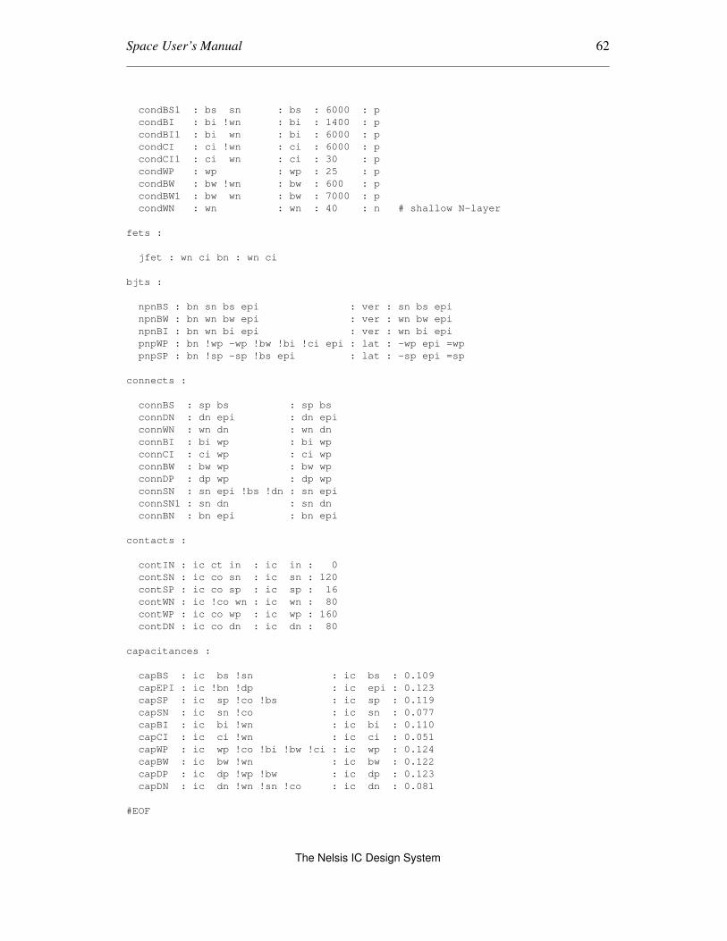
Space User’s Manual 62
condBS1 : bs sn : bs : 6000 : p
condBI : bi !wn : bi : 1400 : p
condBI1 : bi wn : bi : 6000 : p
condCI : ci !wn : ci : 6000 : p
condCI1 : ci wn : ci : 30 : p
condWP : wp : wp : 25 : p
condBW : bw !wn : bw : 600 : p
condBW1 : bw wn : bw : 7000 : p
condWN : wn : wn : 40 : n # shallow N-layer
fets :
jfet : wn ci bn : wn ci
bjts :
npnBS : bn sn bs epi : ver : sn bs epi
npnBW : bn wn bw epi : ver : wn bw epi
npnBI : bn wn bi epi : ver : wn bi epi
pnpWP : bn !wp -wp !bw !bi !ci epi : lat : -wp epi =wp
pnpSP : bn !sp -sp !bs epi : lat : -sp epi =sp
connects :
connBS : sp bs : sp bs
connDN : dn epi : dn epi
connWN : wn dn : wn dn
connBI : bi wp : bi wp
connCI : ci wp : ci wp
connBW : bw wp : bw wp
connDP : dp wp : dp wp
connSN : sn epi !bs !dn : sn epi
connSN1 : sn dn : sn dn
connBN : bn epi : bn epi
contacts :
contIN : ic ct in : ic in : 0
contSN : ic co sn : ic sn : 120
contSP : ic co sp : ic sp : 16
contWN : ic !co wn : ic wn : 80
contWP : ic co wp : ic wp : 160
contDN : ic co dn : ic dn : 80
capacitances :
capBS : ic bs !sn : ic bs : 0.109
capEPI : ic !bn !dp : ic epi : 0.123
capSP : ic sp !co !bs : ic sp : 0.119
capSN : ic sn !co : ic sn : 0.077
capBI : ic bi !wn : ic bi : 0.110
capCI : ic ci !wn : ic ci : 0.051
capWP : ic wp !co !bi !bw !ci : ic wp : 0.124
capBW : ic bw !wn : ic bw : 0.122
capDP : ic dp !wp !bw : ic dp : 0.123
capDN : ic dn !wn !sn !co : ic dn : 0.081
#EOF
The Nelsis IC Design System

Space User’s Manual 63
Appendix G: Parameter File for Bipolar Example Process
#
# space parameter file for DIMES-01 process
#
min_art_degree 3
min_degree 4
min_res 10 # ohm
max_par_res 20
no_neg_res on
min_coup_cap 0.05
lat_cap_window 6.0 # micron
lat_base_width 3.0 # micron
max_obtuse 110.0 # degrees
equi_line_ratio 1.0
The Nelsis IC Design System

Space User’s Manual 64
Appendix H: Control File for Bipolar Example Process
# library_files specifies which file(s) contain
# the appropriate model definitions.
include_library spice3f3.lib
# model indicates which predefined models can be
# used for which group of devices and it includes
# the ranges for area (AE), perimeter (PE) and
# (for lateral pnp) base width (WB).
model bw101a npnBW npn (
AE 4e-12 8e-12 4e-11
PE (2*$AE / 2.00e-06 + 4.00e-06)
)
model bw10x npnBW npn (
AE 4e-12 2e-10
PE 8e-06 6e-05
)
model bs101a npnBS npn (
AE 3.60e-11
PE 2.40e-05
)
model bi101a npnBI npn (
AE 8.00e-12
PE 1.20e-05
)
model wp102c pnpWP pnp (
AE 3.60e-11
PE 2.4e-05
WB 3.00e-06
)
The Nelsis IC Design System

Space User’s Manual 65
Appendix I: Library File for Bipolar Example Process
# In this file, the models are described for the different bipolar
# devices of the DIMES-01 process. It is allowed to create models
# for which the parameters are defined by a substitution equation.
unity Q_electron 1.602e-19
unity N_intrinsic 1.045e+20
unity Gummel_base 7.500e+06
unity C0s_wn_bw 1.900e-03
unity C0e_wn_bw 2.800e-09
unity C0s_bw_epi 0.290e-03
unity C0s_bn_sub 0.151e-03
model bw10x npn (Is=($Q_electron*$N_intrinsic/$Gummel_base)*$AE Nf=1
Ikf=3.00e+07*$AE+6.00e+01*$PE Bf=117 Br=4 Vaf=55 Var=4
Ikr=5.00e+07*$AE+1.00e+02*$PE Xtb=1.5 Eg=1.17 Xti=2.5
Cje=$C0s_wn_bw*$AE+$C0e_wn_bw*$PE Vje=0.78 Mje=0.28 Tf=20p
Xtf=(4.70e-02*$AE+1.90e-02*$PE)ˆ2 Tr=100p Mjc=0.32 Vjc=0.67
Cjc=$C0s_bw_epi*$AE Cjs=$C0s_bn_sub*$AE Vjs=0.45 Mjs=0.26)
model bw101a npn (Is=0.018f Bf=117 Nf=1 Vaf=55 Ikf=4.1m Br=4 Nr=1 Var=4
Ikr=45u Rb=600 Irb=0.15m Rbm=30 Re=14 Rc=200 Xtb=1.5
Eg=1.17 Xti=2.5 Cje=50f Vje=0.78 Mje=0.28 Tf=20p Cjc=75f
Vjc=0.67 Mjc=0.32 Xcjc=1 Tr=100p Cjs=0.24p Vjs=0.45 Mjs=0.26)
model bs101a npn (Is=0.050f Bf=100 Nf=1 Vaf=40 Ikf=5m Ise=1f Ne=2 Br=0.5
Nr=1 Var=5 Ikr=5m Isc=10f Nc=1.2 Rb=350 Irb=1m Rbm=50 Re=25
Rc=150 Eg=1.17 Xti=3 Cje=95f Vje=0.8 Mje=0.26 Tf=30p Cjc=100f
Vjc=0.75 Mjc=0.33 Xcjc=1 Tr=100p Cjs=0.25p Vjs=0.45 Mjs=0.26)
model bi101a npn (Is=0.018f Bf=120 Nf=1 Vaf=58 Ikf=4.2m Br=4 Nr=1 Var=5.8
Ikr=45u Rb=600 Irb=0.15m Rbm=30 Re=14 Rc=200 Xtb=1.5 Eg=1.20
Xti=2.5 Cje=40f Vje=0.77 Mje=0.24 Tf=30p Cjc=75f Vjc=0.65
Mjc=0.32 Xcjc=1 Tr=100p Cjs=0.24p Vjs=0.45 Mjs=0.26)
model wp102c pnp (Is=0.183f Bf=89 Nf=1 Vaf=13 Ikf=0.5m Ise=0.37f Ne=2 BR=17
Nr=1 Var=10 Ikr=0.4m Isc=1.4f Nc=2 Rb=80 Irb=10 Rbm=0 RE=25
Rc=150 Xtb=1.5 Eg=1.20 Xti=2.5 Cje=95f Vje=0.67 Mje=0.34
Tf=90p Cjc=387f Vjc=0.70 Mjc=0.40 Xcjc=0.3 Tr=1n Cjs=0.60p
Vjs=0.52 Mjs=0.31)
The Nelsis IC Design System

CONTENTS
1. Introduction............................................................................................................... 1
1.1 What is Space................................................................................................... 1
1.2 Benefits of Using Space ................................................................................... 1
1.3 Features ............................................................................................................ 2
1.4 Documentation on Space ................................................................................. 3
2. Space Program Usage ............................................................................................... 4
2.1 Introduction...................................................................................................... 4
2.2 General............................................................................................................. 4
2.3 Extraction of Field-effect Transistors .............................................................. 8
2.4 Bipolar Device Extraction................................................................................ 10
2.5 Capacitance Extraction .................................................................................... 10
2.6 Resistance Extraction ....................................................................................... 15
2.7 Frequency Dependent Number of RC Sections ............................................... 20
2.8 Network Reduction Heuristics ......................................................................... 21
2.9 Library Cell Circuit Extraction ........................................................................ 26
2.10 Back Annotation .............................................................................................. 27
2.11 Element Definition Files .................................................................................. 30
2.12 Parameter Files................................................................................................. 31
3. Developing Space Element Definition Files ............................................................. 33
3.1 Introduction...................................................................................................... 33
3.2 Invocation and Command Line Options .......................................................... 33
3.3 Example Technology ....................................................................................... 34
3.4 The Element Definition File............................................................................. 34
3.5 Diagnostics....................................................................................................... 46
4. Preparing Simulation Input ....................................................................................... 47
4.1 Introduction...................................................................................................... 47
4.2 Describing SPICE Models using the Control File of Xspice........................... 48
4.3 The Use of the Program Putdevmod ................................................................ 52
Appendix A: Summary of Command-Line Options...................................................... 54
Appendix B: Hierarchy and Terminals .......................................................................... 56
Appendix C: Solving Problems ..................................................................................... 57
Appendix D: Element Definition File for CMOS Example Process.............................. 58
Appendix E: Parameter File for CMOS Example Process ............................................ 60
Appendix F: Element Definition File for Bipolar Example Process.............................. 61
Appendix G: Parameter File for Bipolar Example Process ........................................... 63
Appendix H: Control File for Bipolar Example Process ............................................... 64
- i -

Appendix I: Library File for Bipolar Example Process ................................................. 65
- ii -