Sliding Mode Control of Photovoltaic Energy Conversion ...
157
Department of Electrical Engineering National Institute of Technology Rourkela Pradeep Kumar Sahu Sliding Mode Control of Photovoltaic Energy Conversion Systems
-
Upload
khangminh22 -
Category
Documents
-
view
2 -
download
0
Transcript of Sliding Mode Control of Photovoltaic Energy Conversion ...
Department of Electrical EngineeringNational Institute of Technology Rourkela
Pradeep Kumar Sahu
Sliding Mode Control of PhotovoltaicEnergy Conversion Systems
November, 2016
Department of Electrical Engineering
National Institute of Technology Rourkela
Sliding Mode Control of PhotovoltaicEnergy Conversion Systems
Dissertation submitted to the
National Institute of Technology Rourkela
in partial fulfillment of the requirements
of the degree of
Doctor of Philosophy
in
Electrical Engineering
by
Pradeep Kumar Sahu
(Roll Number: 511EE701)
under the supervision of
Prof. Somnath Maity
Electrical EngineeringNational Institute of Technology Rourkela
November 11, 2016
Certificate of Examination
Roll Number: 511EE701
Name: Pradeep Kumar Sahu
Title of Dissertation: Sliding Mode Control of Photovoltaic Energy Conversion
Systems
We the below signed, after checking the dissertation mentioned above and the official
record book (s) of the student, hereby state our approval of the dissertation submitted
in partial fulfillment of the requirements of the degree of Doctor of Philosophy in
Electrical Engineering at National Institute of Technology Rourkela. We are satisfied
with the volume, quality, correctness, and originality of the work.
————————— —————————Susovon Samanta Somnath MaityMember (DSC) Principal Supervisor
————————— —————————Santanu Kumar Behera S. P. Singh
Member (DSC) External Examiner
————————— —————————Anup Kumar Panda Jitendriya Kumar SatapathyChairman (DSC) Head of the Department

Electrical EngineeringNational Institute of Technology Rourkela
Prof. Somnath Maity
Assistant Professor
November 11, 2016
Supervisor’s Certificate
This is to certify that the work presented in this dissertation entitled Sliding Mode
Control of Photovoltaic Energy Conversion Systems submitted by Pradeep Kumar
Sahu, Roll Number- 511EE701, is a record of original research carried out by him
under my supervision and guidance in partial fulfillment of the requirements of the
degree of Doctor of Philosophy in Electrical Engineering. Neither this dissertation
nor any part of it has been submitted for any degree or diploma to any institute or
university in India or abroad.
—————————
Somnath Maity
Principal Supervisor

Dedicated
to
my late father

Declaration of Originality
I, Pradeep Kumar Sahu, Roll Number 511EE701 hereby declare that this dissertation
entitled Sliding Mode Control of Photovoltaic Energy Conversion Systems presents
my original work carried out as a doctoral student of NIT Rourkela and, to the best
of my knowledge, it contains no material previously published or written by another
person, nor any material presented for the award of any other degree or diploma
of NIT Rourkela or any other institution. Any contribution made to this research
by others, with whom I have worked at NIT Rourkela or elsewhere, is explicitly
acknowledged in the dissertation. Works of other authors cited in this dissertation
have been duly acknowledged under the sections “Reference”or “Bibliography”. I have
also submitted my original research records to the scrutiny committee for evaluation
of my dissertation.
I am fully aware that in case of any non-compliance detected in future, the Senate
of NIT Rourkela may withdraw the degree awarded to me on the basis of the present
dissertation.
November 11, 2016
NIT RourkelaPradeep Kumar Sahu

Acknowledgment
First of all, I would like to express my deep sense of respect and gratitude towards
my supervisor Prof. Somnath Maity, who has been the guiding force behind this
work. I want to thank him for introducing me to the field of Power Electronics
Converter System and giving me the opportunity to work under him. He has been
supporting and encouraging my research efforts during all my years at NIT Rourkela.
His undivided faith in this topic and ability to bring out the best of analytical and
practical skills in people has been invaluable in tough periods. Without his invaluable
advice and assistance it would not have been possible for me to complete this thesis.
I am greatly indebted to him for his constant encouragement and invaluable advice
in every aspect of my research carrier. I consider it my good fortune to have got an
opportunity to work with such a wonderful person.
I thank our H.O.D. Prof. J. K. Satpathy for the constant support in my thesis
work. I am also grateful to my committee members: Prof. A. K. Panda, Prof. S.
Ghosh, Prof. S. Samanta, and Prof. S. K. Behera for their interests, suggestions and
kind supports for my research work. They have been great sources of inspiration to
me and I thank them from the bottom of my heart.
I would also like to thank all faculty members, all my colleagues in Electrical
Engineering Department; Susanta sir, Ashish, Jitendra, Prem, Sanjeet, and Anneya
to provide me their regular suggestions and encouragements during the whole work.
At last but not the least, I offer my deepest gratitude to my wife Sandhya for
her everlasting love, support, confidence and encouragement for all my endeavors.
Without her, I may lose the motivation to work for my future. Finally, my special
thanks go to my daughter Purvee for giving me such a joy during the tough times as
a Ph.D. student. My family is my eternal source of inspiration in every aspect and
every moment in my life.
November 11, 2016
NIT Rourkela
Pradeep Kumar Sahu
Roll Number: 511EE701
Abstract
Increasing interest and investment in renewable energy give rise to rapid development
of high penetration solar energy. The focus has been on the power electronic converters
which are typically used as interface between the dc output of the photovoltaic (PV)
panels and the terminals of the ac utility network. In the dual-stage grid-connected PV
(GPV) system, the dc-dc stage plays a significant role in converting dc power from PV
panel at low voltage to high dc bus voltage. However, the output of solar arrays varies
due to change in solar irradiation and weather conditions. More importantly, high
initial cost and limited lifespan of PV panels make it more critical to extract as much
power from them as possible. It is, therefore, necessary one to employ the maximum
power point tracking (MPPT) techniques in order to operate PV array at its maximum
power point (MPP). A fast-and-robust analog-MPP tracker is thus proposed by using
the concepts of Utkin’s equivalent control theory and fast-scale stability analysis.
Analytical demonstration has also been presented to show the effectiveness of the
proposed MPPT control technique. After the dc stage, the dc-ac inverter stage is
employed to convert dc power into ac power and feed the power into the utility
grid. The dc-ac stage is realized through the conventional full-bridge voltage source
inverter (VSI) topologies. A fixed frequency hysteresis current (FFHC) controller, as
well as an ellipsoidal switching surface based sliding mode control (SMC) technique
are developed to improve the steady state and dynamic response under sudden
load fluctuation. Such a control strategy is used not only maintains good voltage
regulation, but also exhibits fast dynamic response under sudden load variation.
Moreover, VSI can be synchronized with the ac utility grid. The current injected
into the ac grid obeys the regulations standards (IEEE Std 519 and IEEE Std 1547)
and fulfills the maximum allowable amount of injected current harmonics. Apart from
that, controlling issues of stand-alone and grid-connected operation PV have also been
discussed. A typical stand-alone PV system comprises a solar array and battery which
is used as a backup source for power management between the source and the load.
A control approach is developed for a 1-φ dual-stage transformerless inverter system
to achieve voltage regulation with low steady state error and low total harmonic
distortion (THD) and fast transient response under various load disturbances. The
SMC technique is employed to address the power quality issues. A control technique for
battery charging and discharging is also presented to keep the dc-link voltage constant
during change in load demand or source power. This battery controller is employed for
bidirectional power flow between battery and dc-link through a buck-boost converter
in order to keep the input dc voltage constant. The robust stability of the closed-loop

system is also analyzed. Finally, modeling and control of a 1-φ dual-stage GPV system
has been analyzed. A small-signal average model has been developed for a 1-φ bridge
inverter. The proposed controller has three cascaded control loops. The simulation
results and theoretical analysis indicate that the proposed controller improves the
efficiency of the system by reducing the THD of the injected current to the grid and
increases the robustness of the system against uncertainties.
Keywords: PV system, MPPT, VSI, dual-stage converter topology, SMC,
stand-alone and grid-connected operation.
viii

Contents
Certificate of Examination ii
Supervisor’s Certificate iii
Dedication iv
Declaration of Originality v
Acknowledgement vi
Abstract vii
List of Figures xii
List of Tables xvii
1 Introduction 1
1.1 Motivation . . . . . . . . . . . . . . . . . . . . . . . . . . . . . . . . . . 1
1.2 PV Power System . . . . . . . . . . . . . . . . . . . . . . . . . . . . . . 3
1.2.1 Evolution of PV Cell and Module . . . . . . . . . . . . . . . . . 4
1.2.2 Grid-Connected PV System . . . . . . . . . . . . . . . . . . . . 5
1.3 A Brief Introduction to the String-Inverter Topology . . . . . . . . . . 8
1.4 Existing Inverter Topologies in GPV System . . . . . . . . . . . . . . . 9
1.4.1 Power Processing Stages . . . . . . . . . . . . . . . . . . . . . . 10
1.4.2 Power Decoupling . . . . . . . . . . . . . . . . . . . . . . . . . . 11
1.4.3 Types of Grid Interfacing . . . . . . . . . . . . . . . . . . . . . 12
1.4.4 AC PV Module . . . . . . . . . . . . . . . . . . . . . . . . . . . 13
1.5 Specification, Demand and Standards for GPV Systems . . . . . . . . . 14
1.6 Design Considerations of String-Inverter . . . . . . . . . . . . . . . . . 16
1.7 Objectives of the Research Project . . . . . . . . . . . . . . . . . . . . 17
ix
1.8 Major Contributions and Outline of the Dissertation . . . . . . . . . . 18
2 DC-DC Power Processing 22
2.1 Mathematical Modeling of PV Cell . . . . . . . . . . . . . . . . . . . . 22
2.2 DC-DC Converter Topologies . . . . . . . . . . . . . . . . . . . . . . . 25
2.3 Reviews on MPP Tracker . . . . . . . . . . . . . . . . . . . . . . . . . . 30
2.4 Module-Integrated Analog MPP Trackers . . . . . . . . . . . . . . . . . 33
2.5 Sliding-Mode Controlled MPVS . . . . . . . . . . . . . . . . . . . . . . 38
2.5.1 Existence Conditions Under Ideal Switching Surface . . . . . . . 39
2.5.2 Prediction of Fast-scale Stability Margin . . . . . . . . . . . . . 42
2.5.3 Design Guidelines . . . . . . . . . . . . . . . . . . . . . . . . . . 45
2.5.4 Equivalent SMC and Dynamics of Equivalent Motion . . . . . . 46
2.6 Performance Analysis and Its Experimental Validation . . . . . . . . . 48
2.6.1 Realization of ASMC-Based MPPT . . . . . . . . . . . . . . . . 48
2.6.2 Performance Analysis . . . . . . . . . . . . . . . . . . . . . . . . 50
2.7 Conclusion . . . . . . . . . . . . . . . . . . . . . . . . . . . . . . . . . . 56
3 DC-AC Power Processing 57
3.1 1-φ Inverter Topologies . . . . . . . . . . . . . . . . . . . . . . . . . . . 57
3.2 Modulation Techniques for VSI . . . . . . . . . . . . . . . . . . . . . . 59
3.2.1 1-φ Bridge Topology with Bipolar PWM . . . . . . . . . . . . . 60
3.2.2 1-φ Bridge Topology with Unipolar PWM . . . . . . . . . . . . 61
3.2.3 LC Filter Design for 1-φ VSI . . . . . . . . . . . . . . . . . . . 62
3.3 Classical Control Methods for 1-φ VSI . . . . . . . . . . . . . . . . . . 62
3.4 SMC-Based 1-φ VSI and Its Limitations . . . . . . . . . . . . . . . . . 66
3.5 Constant-Frequency SMC-Based 1-φ VSI . . . . . . . . . . . . . . . . . 67
3.5.1 Constant Frequency Operation . . . . . . . . . . . . . . . . . . 68
3.5.2 Dynamics of 1-φ VSI and Its Mathematical Model . . . . . . . . 69
3.5.3 Experimental Validation . . . . . . . . . . . . . . . . . . . . . . 71
3.5.4 Performance Analysis . . . . . . . . . . . . . . . . . . . . . . . 73
3.6 Selection of an Ellipsoidal Switching Surface . . . . . . . . . . . . . . . 77
3.6.1 Dynamics of 1-φ VSI and Its Mathematical Model . . . . . . . . 78
3.6.2 Performance Analysis . . . . . . . . . . . . . . . . . . . . . . . 79
3.7 Conclusion . . . . . . . . . . . . . . . . . . . . . . . . . . . . . . . . . . 82
4 Single -Phase Grid-Connected Inverter System 83
4.1 1-φ GCI System . . . . . . . . . . . . . . . . . . . . . . . . . . . . . . . 83
4.1.1 Grid-Connected Filter Topologies . . . . . . . . . . . . . . . . . 84
x
4.2 State-of-the-Art of Current Controllers . . . . . . . . . . . . . . . . . . 86
4.2.1 Proposed Control Scheme . . . . . . . . . . . . . . . . . . . . . 88
4.3 SMC in Grid-Connected Inverter System . . . . . . . . . . . . . . . . . 89
4.3.1 Dynamics of 1-φ GCI System and Equation of the SS . . . . . . 90
4.3.2 Existence Condition . . . . . . . . . . . . . . . . . . . . . . . . 91
4.3.3 Stability Condition . . . . . . . . . . . . . . . . . . . . . . . . . 92
4.4 Performance Analysis . . . . . . . . . . . . . . . . . . . . . . . . . . . . 92
4.4.1 Stand-Alone Mode of Operation . . . . . . . . . . . . . . . . . 93
4.4.2 Grid-Connected Mode of Operation . . . . . . . . . . . . . . . 95
4.4.3 Seamless Transfer Mode of Operation . . . . . . . . . . . . . . 98
4.5 Conclusion . . . . . . . . . . . . . . . . . . . . . . . . . . . . . . . . . . 99
5 Dual-Stage Grid-Connected Photovoltaic System 100
5.1 1-φ Standalone PV System . . . . . . . . . . . . . . . . . . . . . . . . . 100
5.1.1 Battery Modeling . . . . . . . . . . . . . . . . . . . . . . . . . . 101
5.1.2 Control Strategies . . . . . . . . . . . . . . . . . . . . . . . . . . 102
5.1.3 Small Signal Stability Analysis . . . . . . . . . . . . . . . . . . 105
5.1.4 Performance Analysis . . . . . . . . . . . . . . . . . . . . . . . . 107
5.2 1-φ Grid-Connected PV System . . . . . . . . . . . . . . . . . . . . . . 112
5.2.1 Two-stage Architecture . . . . . . . . . . . . . . . . . . . . . . . 112
5.2.2 System Control Description . . . . . . . . . . . . . . . . . . . . 112
5.2.3 Modeling of 1-φ GPV System . . . . . . . . . . . . . . . . . . . 113
5.2.4 Closed-Loop Control Design . . . . . . . . . . . . . . . . . . . . 115
5.2.5 Performance Analysis . . . . . . . . . . . . . . . . . . . . . . . . 119
5.3 Conclusion . . . . . . . . . . . . . . . . . . . . . . . . . . . . . . . . . . 122
6 Conclusion 123
6.1 Summary of Contributions . . . . . . . . . . . . . . . . . . . . . . . . . 123
6.2 Future Research Directions . . . . . . . . . . . . . . . . . . . . . . . . . 125
Bibliography 126
Dissemination 138
Dissemination of Work 139
List of Figures
1.1 Overview of PV inverters. (a) Centralized topology. (b) String
topology. (c) Multi-string topology. (d) Module-integrated topology. . . 6
1.2 System diagram of a string-inverter. . . . . . . . . . . . . . . . . . . . . 9
1.3 Three types of power processing stages. (a) Single-stage. (b)
Dual-stage. (c) Three-stage. . . . . . . . . . . . . . . . . . . . . . . . . 10
1.4 Grid-connected inverter. (a) Line-frequency-commutated CSI. (b)
Diode-clamped multi-level VSI. (c) VSI with high frequency PWM
switching. . . . . . . . . . . . . . . . . . . . . . . . . . . . . . . . . . . 13
2.1 Basic PV cell model. . . . . . . . . . . . . . . . . . . . . . . . . . . . . 23
2.2 (a) i-v curve, and (b) p-v curve at different irradiation level. . . . . . . 24
2.3 (a) i-v curve, and (b) p-v curve at different temperature level. . . . . . 24
2.4 Buck converter for PV system. . . . . . . . . . . . . . . . . . . . . . . . 26
2.5 Buck converter circuit for (a) on-state, and (b) off-state operation in
CCM. . . . . . . . . . . . . . . . . . . . . . . . . . . . . . . . . . . . . 26
2.6 Boost converter for PV system. . . . . . . . . . . . . . . . . . . . . . . 28
2.7 Boost converter circuit for (a) on-state, and (b) off-state operation in
CCM. . . . . . . . . . . . . . . . . . . . . . . . . . . . . . . . . . . . . 29
2.8 Buck-Boost converter for PV system. . . . . . . . . . . . . . . . . . . . 30
2.9 The schematic showing the series architecture with a string of two
MPVS and zooming view of analog MPP tracker. . . . . . . . . . . . . 34
2.10 The representative characteristics of v making Vmpp as an attractor. . . 36
2.11 Switching flow diagram of proposed ASMC. . . . . . . . . . . . . . . . 37
2.12 Hysteritic flow of buck-type MIC for io = 4.8A. The other parameters
value used are given in Table 5.1. . . . . . . . . . . . . . . . . . . . . . 38
2.13 Trajectory evolution of ASMC-based MPVS showing the switching and
sliding motion for G = 1000 W/m2, Tc = 25 o C, and io = 4.8 A. The
other parameters value used are given in Table 5.1. . . . . . . . . . . . 41
xii
2.14 Performances of boost-type MIC under enhanced existence region Π
(represented by shadowed region). The parameters value are: L =
140 mH, C = 0.1 µF, and io= 2.3 A. . . . . . . . . . . . . . . . . . . . 42
2.15 Representative bifurcation diagram showing the fast-scale instabilities
of buck-type MIC for L = 140 µH, C = 1000 µF, and io = 5.45 A. Here
T is taken as the bifurcation parameter. . . . . . . . . . . . . . . . . . 46
2.16 Photograph of indoor test set-up of the PV module. . . . . . . . . . . . 49
2.17 Schematic diagram of indoor test set-up. . . . . . . . . . . . . . . . . . 50
2.18 (a) The condition for less transient oscillation under sudden irradiation
variation from 1000 to 400, and then, from 400 to 30 W/m2; and
corresponding experimental validation for irradiation fluctuations: (b)
from 30 to 400; and (c) from 400 to 30 W/m2. CH 1: p (18 W/div),
CH 2: v (10 V/div). All other parameters are same as in Figure 2.13. . 51
2.19 Tracking performance under sudden change of G. . . . . . . . . . . . . 53
2.20 The dynamic response showing the comparison of coupling effects
between Figure 2.9 and P&O based control algorithm for io = 4.8 A.
Here G1 and G2 represent the solar insolations for first and second
module, denoted by M-1 and M-2 respectively. . . . . . . . . . . . . . . 54
2.21 (a) Representative diagram showing the transient performances of Pin
and P do (without any cross-coupling effects) for io = 4.8 A and Req =
0.02 Ω; and (b) its experimental confirmation. CH 1 is the clock pulse
and CH 2 is the input power Pin ≈ 9 W/div. . . . . . . . . . . . . . . . 55
3.1 Schematic diagram of inverter topologies: (a) VSI; (b) CSI. . . . . . . . 58
3.2 PWM techniques for VSI: (a) bipolar; (b) unipolar. . . . . . . . . . . . 61
3.3 Schematic diagram showing: (a) hysteresis function; (b) the state
trajectory in the vicinity of sliding surface S = 0. . . . . . . . . . . . . 67
3.4 The proposed FFHC-controlled 1-φ inverter. . . . . . . . . . . . . . . . 68
3.5 Generation of binary switching pulses S1, S2 over one half cycle, and
the switching sequences of S3, S4 are complementary of power switches
S1, S2 respectively. . . . . . . . . . . . . . . . . . . . . . . . . . . . . . 69
3.6 Laboratory set-up. . . . . . . . . . . . . . . . . . . . . . . . . . . . . . 71
3.7 Steady state behavior of vo and io for a non-linear load. (a) Proposed
FFHC controller. (b) PWM voltage controller proposed in [1]. While
(c) and (d) are the corresponding harmonic spectrum of the output
voltage vo. . . . . . . . . . . . . . . . . . . . . . . . . . . . . . . . . . . 73
3.8 Non-linear load according to IEC62040 standards. . . . . . . . . . . . . 74
xiii

3.9 Steady state response of vo and io. (a) R load. (b) RL load. (c) RC
load. (d) non-linear load. . . . . . . . . . . . . . . . . . . . . . . . . . . 74
3.10 Comparison of transient response between the proposed
FFHC-controller and PWM voltage controller [1] under step load
change from no-load to full load: (a) output voltage vo; (b) load
current io. . . . . . . . . . . . . . . . . . . . . . . . . . . . . . . . . . . 75
3.11 Transient output voltage response of the proposed FFHC-controller
under nonlinear load change from no load to full load condition. . . . . 76
3.12 Comparison of transient response between the proposed
FFHC-controller and PWM voltage controller [1]. The output
voltage waveforms under step load change from full-load to no load
condition. . . . . . . . . . . . . . . . . . . . . . . . . . . . . . . . . . . 76
3.13 The proposed FFSMC-controlled 1-φ inverter. . . . . . . . . . . . . . . 77
3.14 Steady state response at the rated load. (a) Phase plane plot under
proposed ellipsoidal switching surface. (b) Time plot of the of the
output voltage and load current. . . . . . . . . . . . . . . . . . . . . . 80
3.15 Experimental results for v0 and i0 in steady state. (a) R load. (b)
Non-linear load. . . . . . . . . . . . . . . . . . . . . . . . . . . . . . . . 81
3.16 The system trajectory under load fluctuation. (a) Hitting in the
existence region. (b) Hitting in the non-existence region. . . . . . . . . 81
3.17 Transient response of the output voltage and load current of the
proposed controller under step load change from : (a) no-load to full
load; (b) full load to no-load. . . . . . . . . . . . . . . . . . . . . . . . . 81
4.1 1-φ grid-interactive inverter system. . . . . . . . . . . . . . . . . . . . . 84
4.2 Overall control diagram of a 1-φ grid-connected inverter system. . . . . 89
4.3 Laboratory set-up for grid-connected inverter system. . . . . . . . . . . 92
4.4 Stand-alone mode with a resistive load. (a) Steady-state load voltage
v0, 180 shifted reference vref . (b) Load current i0 . . . . . . . . . . . . 93
4.5 Stand-alone mode with the IEC62040 non-linear load. (a) Steady-state
load voltage v0, 180 shifted reference vref . (b) Load current i0. . . . . . 94
4.6 Experimental results of v0 and i0 in stand-alone mode for: (a) R-load;
(b) non-linear load. . . . . . . . . . . . . . . . . . . . . . . . . . . . . . 94
4.7 Transient response of load voltage v0, and load current 10*i0 for a step
load change from open circuit to 20 Ω, and back. . . . . . . . . . . . . 95
4.8 Steady state response in the grid-connected mode. (a) Load current i0
with local load voltage v0. (b) Grid current i2 with the grid voltage vg. 96
xiv
4.9 Transient response of the proposed controller on the absence of the local
load in the grid-connected mode to a step change in I∗. (a) Grid-current
i2, the reference current iref , and the current error ei. (b) Local load
voltage v0, the reference voltage vref and the voltage tracking error ev. . 96
4.10 Transient response in the grid-connected mode for the step load change
from no-load to full load (R=20 Ω) and back. (a) Grid current i2,
its reference iref , and the tracking error current ei. (b) Load current
i0, local load voltage v0 with its reference vref , and the tracking error
voltage ev. . . . . . . . . . . . . . . . . . . . . . . . . . . . . . . . . . . 97
4.11 Seamless transfer response from stand-alone to grid-connected mode
at t = 0.085 s. (a) Grid current i2, its reference iref , and the tracking
error current ei. (b) Local load voltage v0 with its reference vref , and
the tracking error voltage ev. . . . . . . . . . . . . . . . . . . . . . . . . 98
4.12 Seamless transfer response from grid-connected to stand-alone mode at
t = 0.105 s. (a) Grid current i2, reference current iref , and its tracking
error current ei. (b) Local load voltage v0, reference voltage vref , and
tracking error voltage ev. . . . . . . . . . . . . . . . . . . . . . . . . . . 98
5.1 Standalone PV system with battery load. . . . . . . . . . . . . . . . . . 101
5.2 Equivalent circuit of a battery. . . . . . . . . . . . . . . . . . . . . . . . 101
5.3 PV module with analog MPPT control. . . . . . . . . . . . . . . . . . . 103
5.4 Control of bidirectional buck-boost converter. . . . . . . . . . . . . . . 104
5.5 Control of 1-φ inverter. . . . . . . . . . . . . . . . . . . . . . . . . . . . 105
5.6 Control block diagram: (a) bidirectional buck-boost converter; (b)
inverter. . . . . . . . . . . . . . . . . . . . . . . . . . . . . . . . . . . . 106
5.7 Bode diagram: (a) current loop (Li1); (b) voltage loop (Lv1) of
buck-boost converter. . . . . . . . . . . . . . . . . . . . . . . . . . . . . 107
5.8 Bode diagram: (a) current loop (Li2); (b) voltage loop (Lv2) of inverter. 108
5.9 Steady state performance. (a) Output voltage v0. (b) Load current i0
of inverter. . . . . . . . . . . . . . . . . . . . . . . . . . . . . . . . . . . 109
5.10 Steady state performance at nominal condition. (a) DC-link voltage
Vdc. (b) SOC of BSS. . . . . . . . . . . . . . . . . . . . . . . . . . . . . 109
5.11 Transient performance under load variation. (a) Output voltage v0.
(b) Load current i0. . . . . . . . . . . . . . . . . . . . . . . . . . . . . . 110
5.12 Transient performance under load variation. (a) DC-link voltage Vdc.
(b) SOC of BSS. . . . . . . . . . . . . . . . . . . . . . . . . . . . . . . 110
xv
5.13 Transient performance under solar irradiance variation. (a) Output
voltage v0. (b) Load current i0. . . . . . . . . . . . . . . . . . . . . . . 111
5.14 Transient performance under solar irradiance variation. (a) DC-link
voltage Vdc. (b) SOC of BSS. . . . . . . . . . . . . . . . . . . . . . . . 111
5.15 Schematic diagram of a two-stage 1-φ GPV system. . . . . . . . . . . . 113
5.16 Control scheme for the considered GPV system. . . . . . . . . . . . . . 115
5.17 (a) Grid current control diagram. (b) DC-link voltage control diagram . 117
5.18 Bode plot: (a) current control loop with PI controller; (b) dc-link
voltage control loop with PI controller. . . . . . . . . . . . . . . . . . . 118
5.19 Steady-state current waveforms in inverter stage. (a) Inverter side
inductor current i1. (b) Injected grid current i2 with grid-voltage. . . . 119
5.20 % THD of injected grid current i2 at different power level. (a) Rated
output power. (b) 50% of the rated output power. . . . . . . . . . . . . 119
5.21 Current injected into the grid i2 at different power level. (a) 25% of
the rated output power. (b) 50% of the rated output power. . . . . . . 120
5.22 Transient response of the GPV system. (a) Step change of 0 to 50% of
the rated power. (b) Step change of 50% to 100% of the rated output
power. . . . . . . . . . . . . . . . . . . . . . . . . . . . . . . . . . . . . 121
5.23 Transient performance under solar irradiation change. (a) DC-link
voltage. (b) Injected grid current i2 and grid voltage vg. . . . . . . . . . 121
xvi
List of Tables
2.1 Specification of ASMC based modular PV system for G = 1000 W/m2,
and Tc = 25oC . . . . . . . . . . . . . . . . . . . . . . . . . . . . . . . 38
2.2 Dynamics of all three MIC architectures and their representation in the
form of: dxdt
= f + gu , where x = [v i vo]T . . . . . . . . . . . . . . . . 39
2.3 System and input matrices Ai and Bi . . . . . . . . . . . . . . . . . . . 44
2.4 Major Characteristics of MPPT Techniques . . . . . . . . . . . . . . . 52
2.5 η (%) of series configuration for different G1 (W/m2) when io = 4.8 A
and Req= 0.02 Ω . . . . . . . . . . . . . . . . . . . . . . . . . . . . . . 55
4.1 steady-state response in grid-connected mode of operation . . . . . . . 95
5.1 Key Parameters for stand-alone mode . . . . . . . . . . . . . . . . . . . 108
5.2 Key Parameters for grid-connected mode . . . . . . . . . . . . . . . . . 120
xvii
Chapter 1
Introduction
1.1 Motivation
Over the past few decades, distributed generation (DG) has gained lots of attraction
due to the environmentally-friendly nature of renewable energy, the plug-and-play
operation of new generation units, and its ability to offer low installation cost to meet
the challenges of the electricity market [1–8]. DG units provide power at the point of
the load center, which minimizes the losses during power transmission and improves
the power quality to the loads. Furthermore, it can also be used as a backup source
under the absence of grid.
Photovoltaic modules (PV) [9], wind turbines [10], fuel cells [11], and Micro
turbines [12] are used as the sources for the DG units. The DG system powered
by the PV source is commonly used, for its low installation and running cost.
Presently, the energy supplied by the PV source is approximately 1% of the world
energy consumption. Over the past few years, solar power sources demand has grown
consistently due to the following factors: 1) increasing efficiency of solar cells; 2)
manufacturing technology improvement; 3) economies of scale; and 4) can be installed
everywhere. The above factors are making PV system a good candidate to be one
of the most important renewable energy sources of the future. This energy source
increased at a rate of 20-40% per year in the last few years [13]. Moreover, the modular
PV panel configuration of dimension 1 m2 has an average power ratings of hundreds
of watts/panel, broadly adopted by the end consumer. Now all over the world the
largest PV power plant is more than 100MW. Furthermore, the output of PV arrays
is effected by solar irradiation and weather conditions. More importantly, limited
lifespan and high initial cost of PV panels make it more critical to extract as much
1

Chapter 1 Introduction
power from them as possible. Therefore, maximum power point tracking (MPPT)
technique should be realized to accomplish maximum efficiency of PV arrays. Several
algorithms have been developed to achieve MPPT technique.
The PV generation can be generally divided into two types: stand-alone systems
and grid-connected systems. Since PV modules are easily transported from one
place to another, it can be operated in stand-alone mode in remote areas where
the grid is not reachable or is not economical to install. This system can also
suitable for telecommunications units, rural electricity supply, and also auxiliary
power units for emergency services or military applications. Most PV systems were
stand-alone applications until mid-90. A typical stand-alone PV system comprises
of a solar array and a storage device. The storage devices include batteries,
flywheels, super-capacitors, pumped hydroelectric storage and super-conducting
magnetic energy storage devices [14], [15]. Since the solar energy is not possible
throughout the day, a storage device is needed as a backup device in order to make
the electricity available whenever it is needed. Batteries are commonly used in PV
system as a storage device. But the major drawback of the battery in stand-alone
PV systems is its cost factor and the bulky size. So the battery needs to be properly
designed to obtain the optimal efficiency from the PV system.
Another possibility to take advantage of the PV system is injecting the PV power
directly into the existing utility grid. In most parts of the industrially developed
world grid electricity is readily available and can be used as a giant battery to store
all the energy produced by the PV cells. The PV power first supply to the local load
and the rest surplus power is feeding into the grid for the use of other customers.
As a result, the burden on the conventional generation units (e.g. thermal power
plant) is reducing. When the PV power is not sufficiently available (at night or
on cloudy days), then the utility grid can provide power from conventional sources.
Removing the battery from the PV system not only make the system economical but
also increases its reliability. Generally, the lifetime of a PV cell is more than 20 years,
whereas a battery lasts for at most five years and also needs periodic maintenance [16].
A grid-connected photovoltaic (GPV) system comprises a group of energy
transducers, i.e., PV panels and dc-dc converter which converts dc power from PV
panel side voltage to required dc bus voltage. While a dc-ac converter is used as
a power interfacing between the dc PV panels and the ac grid. The dc-ac power
processing stage is achieved by feedback controlled inverter systems. This inverter
must guarantee that it will inject the current into the grid at unit power factor with the
lowest harmonic distortion level. Therefore, PV inverters have an enormous impact
on the performance of PV grid-tie systems. One of the most active area of research
2
Chapter 1 Introduction
for GPV system deals with the way in which the elements of the GPV inverter, PV
panels and power converter stage or stages are arranged to transfer the PV power
to the utility grid efficiently [17]. Among all configuration ”string-inverter” [18] is a
suitable candidate, where each string is connected to one inverter and inject power to
the grid. Since new strings can be easily added to the system to increase its power
rating, system modularity therefore can be maximized. Due to its broadly use and
the possibility to easily add other power converter stages, this configuration has been
chosen as the power conditioning unit considered in this work.
The control strategy of the dc-ac inverter that interfaces the PV array with the
utility grid needs to achieve the following control objectives in order to assure an
efficient energy transfer:
• The control stratey applies to the PV module so as to track the MPP for
maximizing the energy capture. This function must be made at the highest
possible efficiency, over a wide power range, due to the morning-noon-evening
and winter-summer variations.
• The efficient conversion of the input dc power into an ac output current which
has to be injected into the grid. The current injected into the grid must obey
the international standards, such as the IEEE Std. 519 [19] and the IEEE
Std. 1547 [20], which state the maximum allowable amount of injected current
harmonics.
The motivations of this research project are to address the different power processing
stages briefly, i.e., dc-dc stage and dc-ac stage. A proper grid synchronization
technique is selected for connecting the PV system with the utility grid. Then
respective controllers are designed to ensure the requirement for operating at the
MPP imposed by the PV module and requirements for the grid connection specified
by international standards.
1.2 PV Power System
From the functional perspective point of view solar power systems can be divided
into two parts: PV panels, that capture the solar irradiation and transform it into
electrical energy; and power conditioning components, like dc-dc converters, dc-ac
inverters, controllers, etc., which convert the variable voltage dc power into dc or ac
power as per the load requirements.
3
Chapter 1 Introduction
1.2.1 Evolution of PV Cell and Module
Various PV cell technologies by using different materials are available on the present
PV market. Research has been focused on PV cells and materials as it includes almost
half of the system cost. The PV cell technologies are categorized into three generations
based on the manufacturing process and commercial maturity.
The first generation solar cells are based on silicon wafers including
mono-crystalline silicon and multi-crystalline silicon. Mono-crystalline cells have more
efficiency than multi-crystalline cells, but its manufacturing cost is high. These PV
cells have an average efficiency of 12% to 14%. These types of solar cells dominate
the PV market due to their good performance, long life and high stability. These are
mainly mounted on rooftops. However, they are relatively expensive and require a lot
of energy in production.
The second generation solar cells are focused on amorphous silicon thin
film, Copper-Indium-Selenide and Copper-Indium-Gallium-Diselenide thin film, and
Cadmium-Telluride thin film, where the typical performance is 10 to 15%. The
efficiencies of these PV cells are less than first generation. These thin films can be
developed on flexible substrates. As an advantage of thin film solar cells, these can
be developed on large areas up to 6 m2. However, wafer-based solar cell can be only
produced in wafer dimensions. The thin film PV cells are also commonly used in the
recent market.
The third Generation solar cells include nanocrystal-based solar cells,
polymer-based solar cells, dye-sensitized solar cells, and concentrated solar cells.
These are the novel technologies which are promising but are still under development.
Most developed this solar cell types are dye-sensitized and concentrated solar
cell. Dye-sensitized solar cells are based on dye molecules between electrodes.
Electron-hole pairs occurred in dye molecules and transported through nanoparticles
T iO2. Although the efficiency of these PV cells is very low, their cost is also very low.
Their production is smooth concerning other technologies.
Even though all the exciting progress in the cell technologies around the world, PV
cells based on crystalline silicon are commercially used in the market. A cluster of the
PV cells connected in series forms a PV module. The PV modules are mechanically
robust enough to come with a 25 year limited warranty and a guarantee of 1%
power degradation per year. Crystalline silicon modules can be categorized into
mono-crystalline and polycrystalline, also referred as multi-crystalline, silicon type
cells. They consist of front surface glass, encapsulate, 60 to 72 interconnected PV
cells, a back sheet and a metal frame. The standard front surface glass is a low cost
4
Chapter 1 Introduction
transparent tempered low iron glass with self-cleaning properties. This type of glass
is strong, stable under ultraviolet radiation and water and gas impervious. Ethylene
vinyl acetate (EVA) is commonly used as encapsulant material. It helps to keep the
whole module bonded together. EVA is optically transparent and stable under high
temperature and UV radiation. Generally, EVA is placed between a front glass surface
and PV cell, and between back sheet and PV cell. The back sheet is typically made
of Tedlar, which provides protection against moisture and gas ingress. The module
frame is usually made of aluminum. It is believed that these PV modules would
continue to dominate the PV market for at least another decade [21]. This belief is
further strengthened by the recent plummeting of the cost of silicon PV modules.
1.2.2 Grid-Connected PV System
The PV energy generated from sunlight is captured by PV modules. The power
produced by the PV modules are dc electrical power. Integrating the dc power from
the PV modules into the existing ac power distribution network can be achieved
through grid-tie inverters. The inverters must guarantee that the PV modules are
operating at MPP, which is the operating condition where the most energy is captured.
Another function for inverters is to control the current injected into the ac grid
at the same phase with the grid voltage at the lowest harmonic distortion levels.
Therefore, PV inverters have an enormous impact on the performance of GPV
systems. Depending on different levels of MPPT implementation for PV modules,
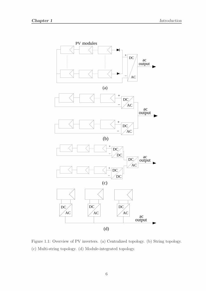
four PV inverter topologies are reported [22], [23], [24].
I. Centralized Topology
The topology shown in Figure 3.1(a) is based on centralized inverters, which
interfaced a large number of modules to the grid [25]. It is commonly used for
large PV systems with the high output power of up to several megawatts. In this
topology, a single inverter is connected to the PV array. The main advantage of
the centralized topology is its low cost as compared to other topologies as well as
the ease maintenance of the inverter. However, this topology has low reliability
as the failure of the inverter will stop the operation of PV system. Moreover,
there is a considerable amount of power loss in the cases of mismatch between
the modules and partial shading, due to the use of one inverter for tracking the
MPP [26], [27].
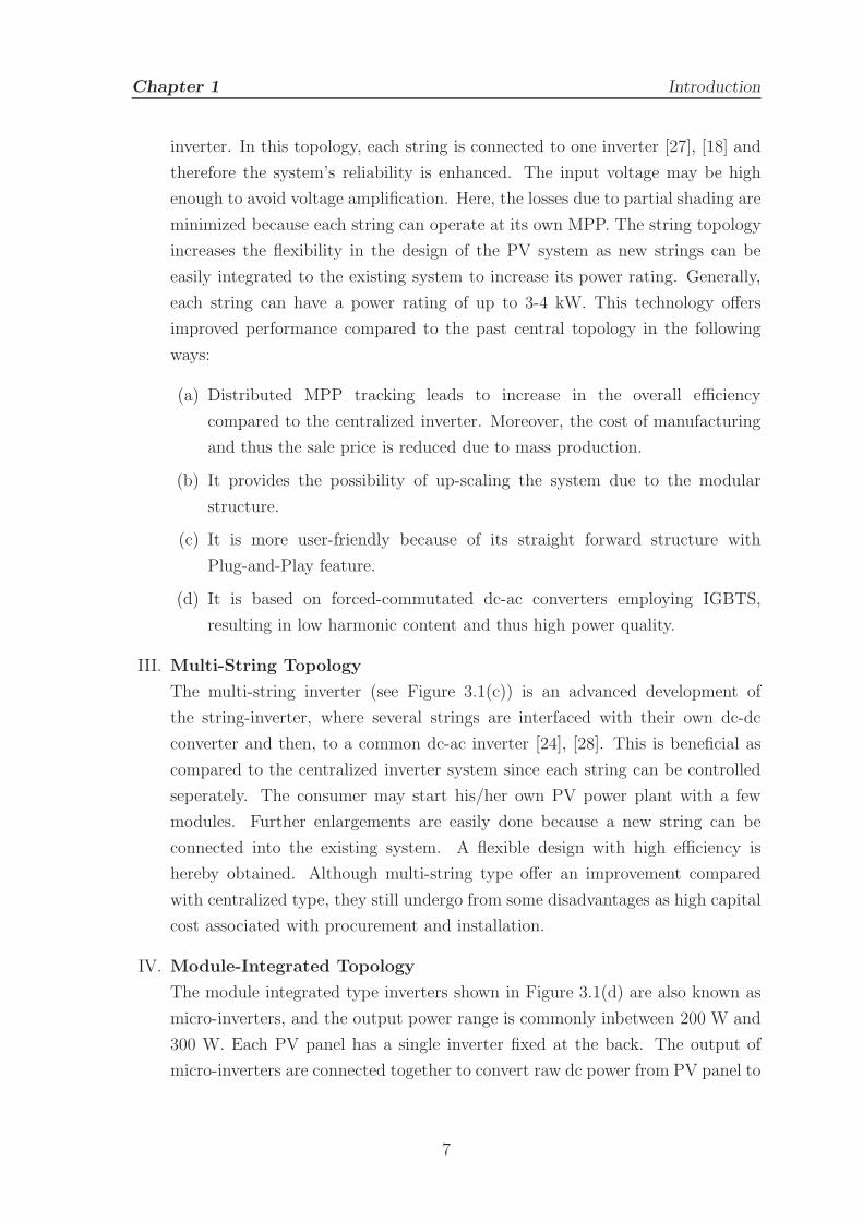
II. String Topology
The string inverter (see Figure 3.1(b)) is an improved version of the centralized
5
Chapter 1 Introduction
(a)
+
−
modulesPV
acoutput
DC
AC
(b)
+
+
−
−
acoutput
DC
AC
DC
AC
(c)
+
+
−
−
ac output
DC
DC
DC
DC
DC
AC
(d)
acoutput
DC
AC
DC
AC
DC
AC
Figure 1.1: Overview of PV inverters. (a) Centralized topology. (b) String topology.
(c) Multi-string topology. (d) Module-integrated topology.
6
Chapter 1 Introduction
inverter. In this topology, each string is connected to one inverter [27], [18] and
therefore the system’s reliability is enhanced. The input voltage may be high
enough to avoid voltage amplification. Here, the losses due to partial shading are
minimized because each string can operate at its own MPP. The string topology
increases the flexibility in the design of the PV system as new strings can be
easily integrated to the existing system to increase its power rating. Generally,
each string can have a power rating of up to 3-4 kW. This technology offers
improved performance compared to the past central topology in the following
ways:
(a) Distributed MPP tracking leads to increase in the overall efficiency
compared to the centralized inverter. Moreover, the cost of manufacturing
and thus the sale price is reduced due to mass production.
(b) It provides the possibility of up-scaling the system due to the modular
structure.
(c) It is more user-friendly because of its straight forward structure with
Plug-and-Play feature.
(d) It is based on forced-commutated dc-ac converters employing IGBTS,
resulting in low harmonic content and thus high power quality.
III. Multi-String Topology
The multi-string inverter (see Figure 3.1(c)) is an advanced development of
the string-inverter, where several strings are interfaced with their own dc-dc
converter and then, to a common dc-ac inverter [24], [28]. This is beneficial as
compared to the centralized inverter system since each string can be controlled
seperately. The consumer may start his/her own PV power plant with a few
modules. Further enlargements are easily done because a new string can be
connected into the existing system. A flexible design with high efficiency is
hereby obtained. Although multi-string type offer an improvement compared
with centralized type, they still undergo from some disadvantages as high capital
cost associated with procurement and installation.
IV. Module-Integrated Topology
The module integrated type inverters shown in Figure 3.1(d) are also known as
micro-inverters, and the output power range is commonly inbetween 200 W and
300 W. Each PV panel has a single inverter fixed at the back. The output of
micro-inverters are connected together to convert raw dc power from PV panel to
7
Chapter 1 Introduction
ac power and inject power into the grid, thus no high voltage dc cable is needed
as centralized type inverters.
Since micro-inverters can perform a dedicate PV power harvest for every single
PV panel, the misleading problems caused by shading, dirt, dust, or other
possible non-uniform changes in irradiations and temperatures are reduced
compared with other types inverters. Moreover, micro-inverters have low dc-link
voltage, thus when failure cases occurred it is easy to repair or replace the
broken part. During this process little affection will happen on the whole power
generation system. These plug-and-play inverters are simple in maintenance,
easily installed, and possible in mass production [28], [29], [30]. In addition they
offer greater flexibility by allowing the use of panels with different specifications,
different ratings, or produced by different manufacturer. Now-a-days, these
inverters would be the development trend of PV system design.
1.3 A Brief Introduction to the String-Inverter
Topology
In order to achieve high dc-link voltage, the PV system employs the string inverter
topology due to its advantages over the central inverter topology. If the dc voltage
level is very high before the inverter, then there is no need of the dc-dc power stage,
otherwise, a dc-dc converter can be used to boost it. For this topology, each string
has connected with its own inverter and therefore the requirement of string diodes is
eliminated leading to reduction in total lossess of the system. This topology allows
individual MPPT for each string; hence, the reliability of the system is enhanced due
to the fact that the system is no longer dependent on only one inverter compared
to the central inverter topology. The mismatch losses are also minimized, but not
eliminated. This leads this topology increases the overall efficiency, with reduction in
cost due to the mass production.
The external connections and internal structure of the string-inverter topology are
shown in Figure 1.2. It consists of two major parts: a power processing part and a
power control part. The power processing part is connected to a PV module on the
input side. The PV module output is fed to the power circuit, which converts the dc
into ac required by the utility. The power circuit may be single stage or two stages.
As the fast switching waveforms of the present day inverter technology would generate
high frequency electromagnetic noise, an low pass passive filter is needed between the
8
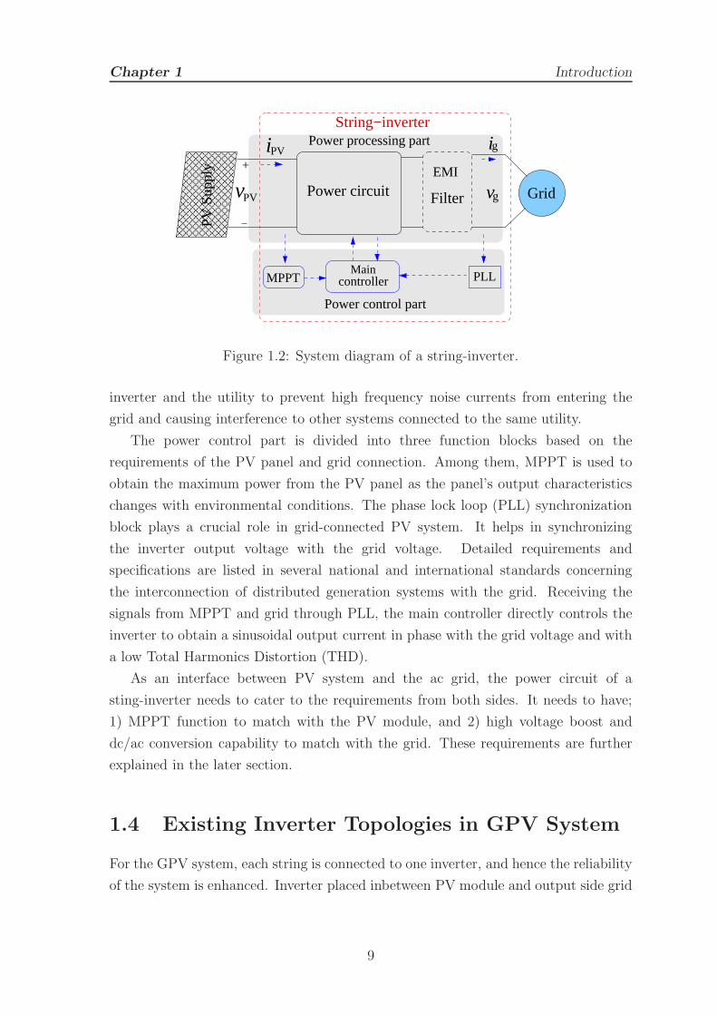
Chapter 1 Introduction
GridPower circuitEMI
Filter
Main controllerMPPT
+
PLL
Power processing part
Power control part
String−inverter
i
v
g
g
i
v
PV
PV
PV
Sup
ply
Figure 1.2: System diagram of a string-inverter.
inverter and the utility to prevent high frequency noise currents from entering the
grid and causing interference to other systems connected to the same utility.
The power control part is divided into three function blocks based on the
requirements of the PV panel and grid connection. Among them, MPPT is used to
obtain the maximum power from the PV panel as the panel’s output characteristics
changes with environmental conditions. The phase lock loop (PLL) synchronization
block plays a crucial role in grid-connected PV system. It helps in synchronizing
the inverter output voltage with the grid voltage. Detailed requirements and
specifications are listed in several national and international standards concerning
the interconnection of distributed generation systems with the grid. Receiving the
signals from MPPT and grid through PLL, the main controller directly controls the
inverter to obtain a sinusoidal output current in phase with the grid voltage and with
a low Total Harmonics Distortion (THD).
As an interface between PV system and the ac grid, the power circuit of a
sting-inverter needs to cater to the requirements from both sides. It needs to have;
1) MPPT function to match with the PV module, and 2) high voltage boost and
dc/ac conversion capability to match with the grid. These requirements are further
explained in the later section.
1.4 Existing Inverter Topologies in GPV System
For the GPV system, each string is connected to one inverter, and hence the reliability
of the system is enhanced. Inverter placed inbetween PV module and output side grid
9
Chapter 1 Introduction
mainly performs three functional operations such as; boost the input voltage, dc-ac
voltage inverting, and MPPT operation. There are different inverters topologies are
reported in the literature. The topologies are classified on the basis of number of
power processing stages, location of power decoupling capacitors with and without
transformer connection, and the types of grid interfacing units.
1.4.1 Power Processing Stages
(a)
PVDC
AC
Grid
(b)
DC
DC AC
DC
Grid
PV
(c)
DC
DC
DC
DC
DC
AC
Grid
PV
Figure 1.3: Three types of power processing stages. (a) Single-stage. (b)
Dual-stage. (c) Three-stage.
The first grouping is the number of cascaded power processing stages. These types of
configuration are used for a string-inverter. Three classes of power processing stages
are shown in Figure 1.3. The inverter shown in Figure 1.3(a) is a single-stage inverter
which must handle all functions itself like - MPPT, grid current control, and voltage
amplification applications. As three functions have to be implemented on a single
stage, the controller need to be much more complicated [18], [31]. Several single stage
inverter topologies with suitable control schemes have been reported in literature [32].
10
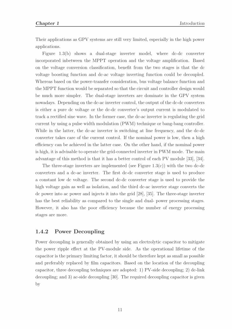
Chapter 1 Introduction
Their applications as GPV systems are still very limited, especially in the high power
applications.
Figure 1.3(b) shows a dual-stage inverter model, where dc-dc converter
incorporated inbetween the MPPT operation and the voltage amplification. Based
on the voltage conversion classification, benefit from the two stages is that the dc
voltage boosting function and dc-ac voltage inverting function could be decoupled.
Whereas based on the power-transfer consideration, bus voltage balance function and
the MPPT function would be separated so that the circuit and controller design would
be much more simpler. The dual-stage inverters are dominate in the GPV system
nowadays. Depending on the dc-ac inverter control, the output of the dc-dc converters
is either a pure dc voltage or the dc-dc converter’s output current is modulated to
track a rectified sine wave. In the former case, the dc-ac inverter is regulating the grid
current by using a pulse width modulation (PWM) technique or bang-bang controller.
While in the latter, the dc-ac inverter is switching at line frequency, and the dc-dc
converter takes care of the current control. If the nominal power is low, then a high
efficiency can be achieved in the latter case. On the other hand, if the nominal power
is high, it is advisable to operate the grid-connected inverter in PWMmode. The main
advantage of this method is that it has a better control of each PV module [33], [34].
The three-stage inverters are implemented (see Figure 1.3(c)) with the two dc-dc
converters and a dc-ac inverter. The first dc-dc converter stage is used to produce
a constant low dc voltage. The second dc-dc converter stage is used to provide the
high voltage gain as well as isolation, and the third dc-ac inverter stage converts the
dc power into ac power and injects it into the grid [28], [35]. The three-stage inverter
has the best reliability as compared to the single and dual- power processing stages.
However, it also has the poor efficiency because the number of energy processing
stages are more.
1.4.2 Power Decoupling
Power decoupling is generally obtained by using an electrolytic capacitor to mitigate
the power ripple effect at the PV-module side. As the operational lifetime of the
capacitor is the primary limiting factor, it should be therefore kept as small as possible
and preferably replaced by film capacitors. Based on the location of the decoupling
capacitor, three decoupling techniques are adopted: 1) PV-side decoupling; 2) dc-link
decoupling; and 3) ac-side decoupling [30]. The required decoupling capacitor is given
by
11
Chapter 1 Introduction
C =PPV
2ωgVc∆V(1.1)
where PPV is the PV modules’ nominal power, Vc is the capacitor voltage, and ∆V
is the ripple voltage. From (1.1) it can be calculated that a parallel capacitor of 2.4
µF is required across the PV module for VMPP = 35 V, ∆V = 3 V, and PMPP = 160
W. However, if the capacitor is located at the dc link, it is sufficient to use 33 µF at
400 V with a ripple voltage of 20 V for the same PV module. In this work, dc-link
decoupling technique is used due to high PV nominal voltage.
1.4.3 Types of Grid Interfacing
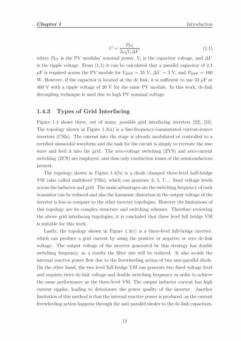
Figure 1.4 shows three, out of many, possible grid interfacing inverters [22], [24].
The topology shown in Figure 1.4(a) is a line-frequency-commutated current-source
inverters (CSIs). The current into the stage is already modulated or controlled to a
rectified sinusoidal waveform and the task for the circuit is simply to recreate the sine
wave and feed it into the grid. The zero-voltage switching (ZVS) and zero-current
switching (ZCS) are employed, and thus only conduction losses of the semiconductors
present.
The topology shown in Figure 1.4(b) is a diode clamped three-level half-bridge
VSI (also called multilevel VSIs), which can generate 3, 5, 7.... fixed voltage levels
across the inductor and grid. The main advantages are the switching frequency of each
transistor can be reduced and also the harmonic distortion in the output voltage of the
inverter is less as compare to the other inverter topologies. However the limitations of
this topology are its complex structure and switching schemes. Therefore reviewing
the above grid interfacing topologies, it is concluded that three level full bridge VSI
is suitable for this work.
Lastly, the topology shown in Figure 1.4(c) is a three-level full-bridge inverter,
which can produce a grid current by using the positive or negative or zero dc-link
voltage. The output voltage of the inverter generated by this strategy has double
switching frequency, as a results the filter size will be reduced. It also avoids the
internal reactive power flow due to the freewheeling action of two anti-parallel diode.
On the other hand, the two level full-bridge VSI can generate two fixed voltage level
and requires twice dc-link voltage and double switching frequency in order to achieve
the same performance as the three-level VSI. The output inductor current has high
current ripples, leading to deteriorate the power quality of the inverter. Another
limitation of this method is that the internal reactive power is produced, as the current
freewheeling action happens through the anti parallel diodes to the dc-link capacitors.
12
Chapter 1 Introduction
21 ig
21 ig
(a)
Grid
dcV2
dcV2
+
+
−
− i
L
g
gGrid
(b)
+
− L
gi
gGrid
(c)
Vdc
Figure 1.4: Grid-connected inverter. (a) Line-frequency-commutated CSI. (b)
Diode-clamped multi-level VSI. (c) VSI with high frequency PWM switching.
The controlled pulses for the switches in the VSI and the reference for the
grid-current waveform are mostly based on measured grid voltage or zero-crossing
detection. But the above methods are not suitable under the distorted grid
condition [36]. The above problem can be solved by using a phase-locked loop (PLL),
as it collects the grid voltage phase information and generates a pure sinusoidal
reference current for the grid.
1.4.4 AC PV Module
AC PV module is also known as the PV panel integrated with a micro-inverter as
shown in Figure 3.1(d). The output ac power of a PV module could be directly
13
Chapter 1 Introduction
connected to a utility grid. The concept was first suggested by Caltech’s Jet
Propulsion Laboratory [37] in the 1970s. From the 1990s, this technology of ac module
is developed rapidly with the support from the government. With many advantages
over central inverter systems, the ac PV module is treated as the future development
trend of PV solar power systems. The rated ac power of a PV module could be in the
range of 100W or even less. Thus, the minimum system could be as small as 100W
or even less. With required power size increasing, more and more ac modules could
be integrated to the existing system. The system capacity could be increased to any
desired power range. So these are more suitable for both residential PV system and
PV farm system. With the flexible system size, the ac PV module has significant
market potential.
1.5 Specification, Demand and Standards for GPV
Systems
Inverter interfacing to the GPV system should have two primary tasks. One is to
operate the PV system at the MPP. The other task is to inject a sinusoidal current
into the grid with unity power factor. The above two functions are broadly discussed
here.
I. Demands Defined by the Grid
The utility companies must maintain an approved standard for the
grid-connected DG system. Here, the present international standard
IEEE-1547 [20] and the future standard IEC-61727 [19] are worth considering.
These measures involve with issues like detection of stand-alone operation,
power quality, and grounding. Detection of stand-alone operation is essential
for the inverter, as it take appropriate measures to protect equipment. Under
stand-alone operation, the grid is disconnected from the inverter so that it will
supply power to the local loads. The detection methods are commonly classified
into two categories, such as active and passive. Since this work is focused on
the seamless transfer method, so that the above stand-alone detection methods
will not be discussed. The IEEE-1547 [20] standards have limitations on the
maximum allowable injected dc current into the grid to avoid saturation of the
distribution transformers [38]. The range of the dc current is about 0.5% to
1% of the rated output current. This problem can be solved by connecting a
line-frequency transformer between the grid and the inverter. Assuming that
14
Chapter 1 Introduction
the grid voltage and grid current are free from harmonics and both are in phase.
Then, the instantaneous power injected to the grid is given by
pg = 2P sin2(ωgt) (1.2)
where P is the average power, ωg is the angular grid frequency, and t is the time.
II. Demands Defined by PV Modules
The inverters must ensure that the PV module(s) is operated at the MPP so
that maximum energy can be captured from the module(s). This is achieved by
an MPP tracker. It also takes into account that the voltage ripple appears at
the PV module(s) terminals should be sufficiently small, as it operates around
the MPP without considerable fluctuation. The ripple voltage amplitude and
the utilization ratio has a relationship, given as [22]
∆V =
√
(2Upv − 1)PMPP
3αVMPP + β(1.3)
where ∆V is the ripple voltage amplitude, Upv is the utilization factor which is
the ratio between the generated average power to the calculated MPP power,
VMPP, and PMPP are the PV voltage and power at MPP, α and β are the
coefficients representing a second-order Taylor approximation of the current.
It is calculated that 98% utilization ratio can be achieved at the ripple voltage
amplitude less than 8.5%. As seen in (1.2), the pulsating power of double grid
frequency is injected to the grid, so a power decoupling device must require for
the inverter.
III. Demands Defined by the User
Finally, the owner (the user) also has to say few words. The users demand a
low-cost, reliable inverter topology, a high efficiency over a wide variation of
the input voltage and input power, as both the variables depend on the solar
irradiation and ambient temperature. The user also demands long operational
lifetime warranty of 10 to 15 years at an efficiency of 75%, and a material and
service warranty of 5 years. But the electrolyte capacitor used in the inverter as
a power decoupling device between the PV module and utility grid [39] is the
principal limiting component.The operational lifetime of an electrolytic capacitor
is given by [40]
TOT = TOT,00.2
(
T0−Th∆T
)
(1.4)
where TOT is the operational lifetime, TOT,0 is the lifetime at T0, Th is the hotspot
temperature, and ∆T is the rise temperature. However, the operational lifetime
of the capacitor can be improved when the inverter are placed indoors.
15
Chapter 1 Introduction
From the above discussion, it can be observed that inverter plays a significant role
in the grid-connected PV system. Such a design of the inverter is given in the next
section.
1.6 Design Considerations of String-Inverter
Based on the previous analysis and discussion (see Section 1.2.2) of the PV power
generation systems, the string-inverter topology is selected to establish the PV system
in this thesis. Since the performance of this inverter is determined by the factors such
as; isolation, efficiency, reliability, and power density, these factors should be kept in
mind for designing of an inverter.
• Isolation: In the grid-connected system, isolation is required in PV installation.
The isolation is realized through a transformer. But the use of transformers,
system becomes bulky, heavy, and expensive. Even though significant size and
reduction in weight can be obtained with high frequency transformer, the use of
transformer still deteriorates the efficiency of the entire PV system. Therefore,
transformerless PV systems are commonly used to overcome these issues. They
are smaller, lighter, lower in cost, and highly efficient [41].
• Efficiency: The efficiency of the overall system is determined by PV panel
efficiency, MPPT performance and inverter conversion efficiency. The PV
panel efficiency is determined by selecting one of the PV cell technology as
discussed in Section 1.2.1, where MPPT is the prime component for tracking
the maximum power of PV panel continuously under changing environmental
condition (i.e., solar irradiance and temperature). The MPPT performance
or tracking efficiency is assessed with static and dynamic condition. The
commercial inverter MPPT efficiency is always greater than 98%. The inverter
conversion efficiency is a weighed conversion efficiency that considers several
operating conditions [42]. The inverter conversion efficiency is the crucial factor
from the investor point of view.
• Power Density and Reliability Issues: The power density is an important
factor to decrease the volume and cost of the inverter. Since the number of
modules in a string is connected to a single inverter (see Figure 3.1(b)), the
volume is preferred to be small. Most commercial PV modules are guaranteed
to perform at specified levels of output for 20 to 25 years [43]. Integrating
the inverter to the PV module necessitates that they both must have matched
16

Chapter 1 Introduction
expected lifetimes so that the inverter should also have a lifetime for 20 to 25
years.
Based on these above factors, a few design guidelines can be given for string-inverters
as:
1. Out of single, dual, and three-stage inverters, a dual-stage inverter structure is
suitable because of its better efficiency with high-quality (low THD) ac output
voltage.
2. Selection of proper switching technique which would improve the inverter
conversion efficiency as well as the power density.
3. Considering isolation requirement, as low-frequency transformer is not only large
but also power consuming, so the transformerless topology should be selected
in the inverter design.
4. The capacitance of system is preferred to be the smaller and better to improve
the reliability.
1.7 Objectives of the Research Project
This research work aims at broadly developing new control algorithms for the PV
system interface that guarantee stable and high power quality injection under the
network disturbances and uncertainties. Although the advantages of dual-stage
string-inverters have been recognized as a suitable one, wide adoption of GPV system
still presents many challenges. This research work is focused on addressing these
challenges with the following objectives.
• Improved MPPT Performance
To maximize the output power of a PV system, continuously tracking the MPP
of the system is necessary. The main challenges for MPPT of a solar PV array
include: 1) how to track an MPP quickly, 2) how to stabilize at an MPP, and
3) how to make a smooth transition from one MPP to another under sharply
changing weather conditions. In general, designing a fast and robust MPPT
controller (with high tracking performance) for the GPV system is a challenging
task. In order to effective design and development of solar PV systems, it
is important to investigate and compare the performance, and advantages or
disadvantages of conventional MPPT techniques used in the solar PV industry,
17
Chapter 1 Introduction
and develop a new MPPT technique for fast and reliable extraction of solar PV
power.
• Power Quality and Efficiency Issues
A PV system can be operated in stand-alone mode or grid-connected mode.
Maintaining good voltage regulation and achieving fast dynamic response under
sudden load fluctuation are extremely important in stand-alone PV systems.
Moreover, the THD of inverter output voltage should be within the limit even
for nonlinear loads. In the grid-connected mode of operation, it is important
to inject a low THD current from PV system to grid at unity power factor.
Nowadays, research is focused to achieve low THD for the local load voltage and
the injected grid current simultaneously. Growing demand for maximized energy
extraction from PV sources have stimulated substantial technology development
efforts towards high-efficiency PV grid-connected inverters.
1.8 Major Contributions and Outline of the
Dissertation
The following are the most significant contribution of this thesis:
1. This research work proposes a fast and robust analog-MPP tracker (also called as
analog sliding-mode controller (ASMC)) which is implemented and designed by
using the concepts of Utkin’s equivalent control theory and fast-scale stability
analysis. The main objectives of applying such concepts are to provide the
control support for the MPPT system which are required for 1) guaranteed
stability with high robustness against the parameters uncertainties, and 2) fast
dynamic responses under rapidly varying environmental conditions. This cannot
be met by conventional digital or analog MPPT controllers without continuously
tuning the controller parameters and complex controller architecture. Thus,
the choice of this analog solution is quite attractive because of its low cost
and capability of easy integration with a conventional dc-dc converter in the
integrated circuit (IC) form, so that plug-and-play operation for many low power
residential PV applications can be easily achieved.
2. Maintaining good voltage regulation and achieving fast dynamic response under
sudden load fluctuation are extremely important in stand-alone PV systems. In
this work, a fixed frequency hysteresis current (FFHC) controller is proposed,
18
Chapter 1 Introduction
which is implemented on the basis of sliding mode control (SMC) technique
and fixed frequency current controller with a hysteresis band. This has been
verified and compared with the carrier based pulse width modulated (PWM)
voltage controller under the same load fluctuation. The proposed method is
then applied to a prototype 1kVA, 110V, 50Hz 1-φ voltage source inverter (VSI)
system. The results show that the dynamic response is quite faster than that of
widely used PWM-controlled inverter systems. Moreover, the THD of inverter
output voltage is less at standard nonlinear load IEC62040-3.
3. A PV system can be connected to the utility grid, injecting power into the
grid besides providing power to their local loads. In this work, a cascaded
SMC strategy is proposed for a grid-connected inverter system to simultaneously
improve the power quality of the local load voltage and the current exchanged
with the grid. The proposed controller also enables seamless transfer operation
from stand-alone mode to grid-connected mode and vice versa. The proposed
method is then applied to 1-kVA, 110V, 50Hz grid-connected 1-φ VSI system.
The results show that the steady-state response and the dynamic response are
quite attractive.
4. Finally, a typical stand-alone PV system comprises of a solar array and a storage
device i.e., battery. In this mode of operation, the battery is used as a backup
source for power management between the source and the load. Lead-acid
battery is used in high power PV applications due to its low cost and availability
in large size. The modeling of a lead-acid battery by using the equivalent circuits
are discussed here. Three independent control loops are proposed to control the
standalone PV system; MPPT control loop for extracting maximum power from
PV module, battery control loop for bidirectional power flow between battery
and dc-link through buck-boost converter to keep the input dc voltage constant
and inverter control loop for maintaining good voltage regulation and achieving
fast dynamic response under sudden load fluctuations. Similarly, a cascaded
sliding mode control is proposed for GPV system to regulate the current from
PV system to the grid at a lower THD level.
The dissertation will be organized as following:
Chapter-1 gives a brief introduction of the PV system. The renewable energy
sources have gained lots of attraction due to the environmentally-friendly nature, and
the plug-and-play operation. Among various renewable energy sources, solar energy
is commonly used, for its low installation and running cost. It is extremely suitable
19
Chapter 1 Introduction
for large-scale power generation. The PV system consists of two major parts: a power
processing part and a power control part. The power processing part have been
analyzed carefully, which is the objective of this thesis. Based on the considerations
of efficiency, power density, galvanic isolation and reliability, several restrictions are
reviewed to guide the particular design of the inverter.
Chapter-2 provides the brief study of dc-dc power processing stage. The dc-dc
converter plays a major role in dual stage PV system in converting dc power from PV
panel at low voltage to high dc bus voltage. Out of various topologies, conventional
non-isolated dc-dc converters have been studied. A novel MPPT with fast tracking
performance and guaranteed stability with high robustness against the parameters
uncertainties is proposed to track the maximum power from the PV modules. The
feasibility of the proposed MPPT method is proved mathematically. Finally, the
analytical results have been validated with the help of simulations and experiments.
Chapter-3 provides the study of dc-ac power processing stage. A brief
introduction is given on dc-ac inverter topologies. To improve the inverter efficiency,
the modulation technique should be employed. Thus, a review of the modulation
techniques on inverters is given. The stand-alone mode of operation with a fixed dc
supply will be considered here. Maintaining good voltage regulation and achieving fast
dynamic response under sudden load fluctuation are vital for a dc-ac inverter system.
The SMC is proposed to meet the above requirements. Simulation and experiment
results verify the theory analysis.
Chapter-4 provides the grid integration of the PV system. In this chapter, the dc
source is interfaced with utility grid through a single-phase inverter. It is important
to inject a low THD current from PV system to grid at unity power factor. This can
be achieved by using a phase lock loop (PLL), which collects the grid voltage phase
information and produce the reference current for the Inverter. Moreover, the analysis
and design of a single-phase inverter system including inductor-capacitor-inductor
(LCL) filter and the phase-lock loop is discussed here. A cascaded SMC controller
has been designed to meet the above power quality issues as well as to achieve the
seamless transfer operation. Simulation and experiment results also verify the theory
analysis.
Chapter-5 provides the GPV operation, which is formed by combining all the
power processing stages, discussed in the previous chapters. The PV system can either
be connected in standalone mode or grid-connected mode. A typical stand-alone PV
system comprises of a solar array and a storage device i.e., battery. The modeling
of a commonly used battery, i.e., lead-acid battery by using the equivalent circuits
are discussed in this chapter. Separate controllers are proposed for the both mode of
20

Chapter 1 Introduction
operation to address the power quality issues discussed in Chapter-1.
Chapter-6 summarizes the whole thesis and describes the future work developed.
21
Chapter 2
DC-DC Power Processing
The dc-dc converter plays an important role in dual-stage PV system in converting
dc power from PV panel at low voltage to high dc bus voltage. The input side of the
dc-dc converter is connected with the PV source, which leads a wide range of input
voltage fluctuation due to change in operating condition of the PV cells. The function
of the converter is to keep the output voltage constant. Again the output power of
the PV source is continually affected by the environmental factors like irradiation
and temperature. The MPPT is used to control dc-dc converter such that the power
extracted from PV panel is maximized. The mathematical modeling of PV cell, review
of various dc-dc converter topologies, and Implementation of a fast tracking MPPT
will be discussed in this chapter.
2.1 Mathematical Modeling of PV Cell
Nowadays, PV cells are manufactured based on the p-n junction crystalline silicon
materials. The behavior of PV cells can be approximated by a common diode equation.
The basic PV cell model is presented in Figure 2.1, which is a p-n junction diode in
parallel with a constant current source [21]. This single diode model can also be used
to find out the electrical behavior of N series PV cells. Here, iPV represents the light
induced current, Rsh and Rs are the shunt and series resistance respectively. The
parallel resistance Rsh accounting for current leakage through the cell, around the
edge of the device, and between contacts of different polarity. The series resistance Rs
causes an extra voltage drop between the junction voltage and the terminal voltage of
the solar cell. The current iPV is proportional to the solar radiation (insolation) and
the resistances represents the various losses. The current flowing through the diode
22
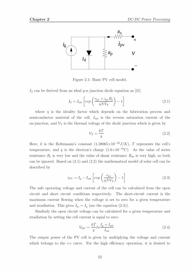
Chapter 2 DC-DC Power Processing
−
+
IR
R
iv
d
p
s
pvgI
Figure 2.1: Basic PV cell model.
Id can be derived from an ideal p-n junction diode equation as [21]
Id = Isat
[
exp
(vpv + ipvRs
ηNVT
)
− 1
]
(2.1)
where η is the ideality factor which depends on the fabrication process and
semiconductor material of the cell, Isat is the reverse saturation current of the
on-junction, and VT is the thermal voltage of the diode junction which is given by
VT =kT
q(2.2)
Here, k is the Boltzmann’s constant (1.38065×10⁻²³J/K), T represents the cell’s
temperature, and q is the electron’s charge (1.6×10⁻¹⁹C). As the value of series
resistance Rs is very low and the value of shunt resistance Rsh is very high, so both
can be ignored. Based on (2.1) and (2.2) the mathematical model of solar cell can be
described by
iPV = Ig − Isat
[
exp
(vpv
ηNVT
)
− 1
]
(2.3)
The safe operating voltage and current of the cell can be calculated from the open
circuit and short circuit conditions respectively. The short-circuit current is the
maximum current flowing when the voltage is set to zero for a given temperature
and irradiation. This gives Isc = Ig (see the equation (2.3)).
Similarly the open circuit voltage can be calculated for a given temperature and
irradiation by setting the cell current is equal to zero:
VOC =kT
qlnIg + Isat
Isat(2.4)
The output power of the PV cell is given by multiplying the voltage and current
which belongs to the i-v curve. For the high efficiency operation, it is desired to
23
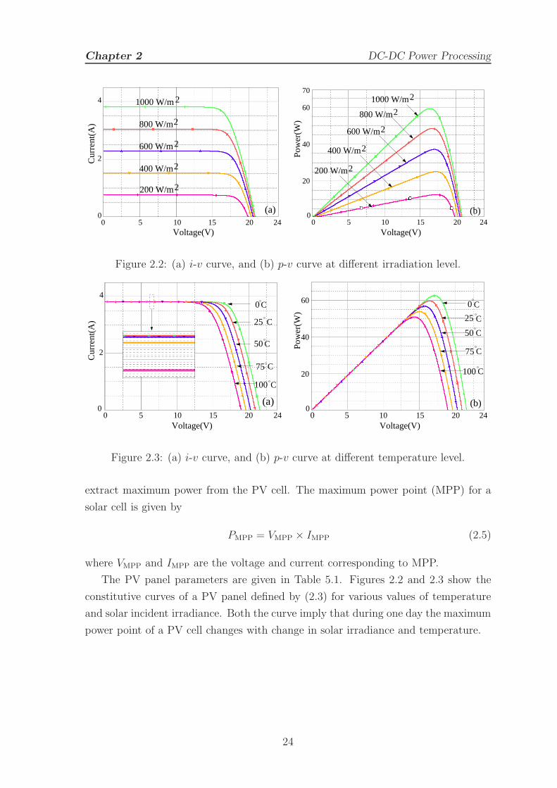
Chapter 2 DC-DC Power Processing
(a)
1000 W/m
800 W/m
600 W/m
400 W/m
200 W/m
2
2
2
2
2
Cur
rent
(A)
Voltage(V)0 5 10 15 20 24
0
2
4
800 W/m
600 W/m
400 W/m
2
2
2
2
2200 W/m
Pow
er(W
)
1000 W/m
Voltage(V)2420151050
0
20
40
60
70
(b)
Figure 2.2: (a) i-v curve, and (b) p-v curve at different irradiation level.
0
4
(a)
25
50
0
C
C
C
C
75
100 C
Voltage(V)
Cur
rent
(A)
0 5 10 15 20 24
2
(b)
0 C
25 C
C
75C
Pow
er(W
)
50
C100
Voltage(V)0 5 10 15 20 24
0
60
40
20
Figure 2.3: (a) i-v curve, and (b) p-v curve at different temperature level.
extract maximum power from the PV cell. The maximum power point (MPP) for a
solar cell is given by
PMPP = VMPP × IMPP (2.5)
where VMPP and IMPP are the voltage and current corresponding to MPP.
The PV panel parameters are given in Table 5.1. Figures 2.2 and 2.3 show the
constitutive curves of a PV panel defined by (2.3) for various values of temperature
and solar incident irradiance. Both the curve imply that during one day the maximum
power point of a PV cell changes with change in solar irradiance and temperature.
24
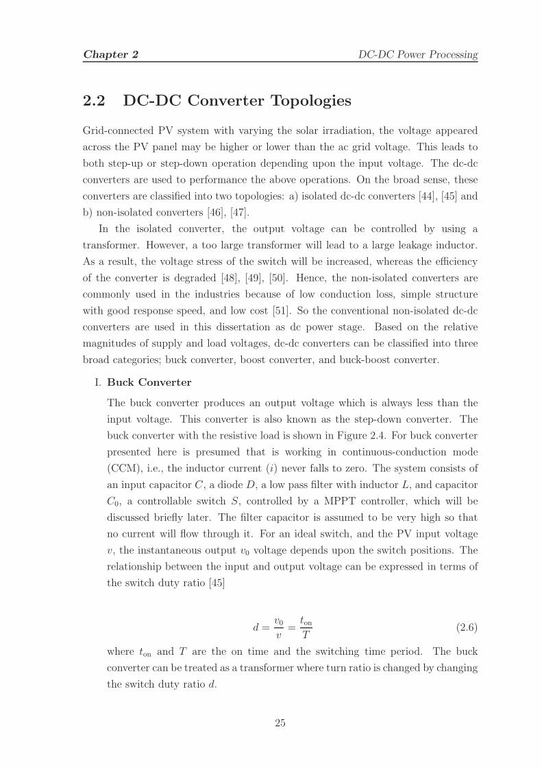
Chapter 2 DC-DC Power Processing
2.2 DC-DC Converter Topologies
Grid-connected PV system with varying the solar irradiation, the voltage appeared
across the PV panel may be higher or lower than the ac grid voltage. This leads to
both step-up or step-down operation depending upon the input voltage. The dc-dc
converters are used to performance the above operations. On the broad sense, these
converters are classified into two topologies: a) isolated dc-dc converters [44], [45] and
b) non-isolated converters [46], [47].
In the isolated converter, the output voltage can be controlled by using a
transformer. However, a too large transformer will lead to a large leakage inductor.
As a result, the voltage stress of the switch will be increased, whereas the efficiency
of the converter is degraded [48], [49], [50]. Hence, the non-isolated converters are
commonly used in the industries because of low conduction loss, simple structure
with good response speed, and low cost [51]. So the conventional non-isolated dc-dc
converters are used in this dissertation as dc power stage. Based on the relative
magnitudes of supply and load voltages, dc-dc converters can be classified into three
broad categories; buck converter, boost converter, and buck-boost converter.
I. Buck Converter
The buck converter produces an output voltage which is always less than the
input voltage. This converter is also known as the step-down converter. The
buck converter with the resistive load is shown in Figure 2.4. For buck converter
presented here is presumed that is working in continuous-conduction mode
(CCM), i.e., the inductor current (i) never falls to zero. The system consists of
an input capacitor C, a diode D, a low pass filter with inductor L, and capacitor
C0, a controllable switch S, controlled by a MPPT controller, which will be
discussed briefly later. The filter capacitor is assumed to be very high so that
no current will flow through it. For an ideal switch, and the PV input voltage
v, the instantaneous output v0 voltage depends upon the switch positions. The
relationship between the input and output voltage can be expressed in terms of
the switch duty ratio [45]
d =v0v
=tonT
(2.6)
where ton and T are the on time and the switching time period. The buck
converter can be treated as a transformer where turn ratio is changed by changing
the switch duty ratio d.
25
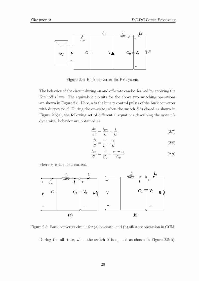
Chapter 2 DC-DC Power Processing
+
−
i
0
+
−
PV
iL
Cv
i
PV D
S
C
0
Rv0
Figure 2.4: Buck converter for PV system.
The behavior of the circuit during on and off-state can be derived by applying the
Kirchoff’s laws. The equivalent circuits for the above two switching operations
are shown in Figure 2.5. Here, u is the binary control pulses of the buck converter
with duty-ratio d. During the on-state, when the switch S is closed as shown in
Figure 2.5(a), the following set of differential equations describing the system’s
dynamical behavior are obtained as
dv
dt=
iPVC
− i
C(2.7)
di
dt=
v
L− v0
L(2.8)
dv0dt
=i
C0
− v0 − i0C0
(2.9)
where i0 is the load current.
+
−
+
−
vC R
L
C 0
i ii
PV
0
v
(a)
0
+
−
+
−
v
L
v
i
R0C0
i0
(b)
Figure 2.5: Buck converter circuit for (a) on-state, and (b) off-state operation in CCM.
During the off-state, when the switch S is opened as shown in Figure 2.5(b),
26

Chapter 2 DC-DC Power Processing
then
dv
dt=
iPVC
(2.10)
di
dt= −v0
L(2.11)
dv0dt
=i
C0− v0 − i0
C0(2.12)
If u is the control signal for controlling the switch S, then (2.7)-(2.12) can be
rewritten as
dv
dt=
iPVC
− i
Cu (2.13)
di
dt=
v
Lu− v0
L(2.14)
dv0dt
=i
C0− v0 − i0
C0(2.15)
The dynamics of the buck converter can be written in state space form as
dx
dt= f + gu (2.16)
where x =
v
i
v0
, f =
iPVCx3
L
x2
C0−x3 − io
C0
, g =
x2
Cx1
L
0
, and u =
[
1
0
]
.
A dc-dc buck converter and an MPPT control circuit are required to provide the
controlled switching pulses to the converter so that it forces the operating point
of the PV system close to the desired value.
II. Boost Converter
The boost converters are commonly used to extract the maximum power from
the PV array. These converters produce an output voltage which is higher than
the input voltage. When the PV voltage is insufficient, the PV voltage can be
boosted with the use of the boost converter. The basic circuit design of a boost
converter is shown in Figure 2.6. The boost converter absorbs and supplies
energy from PV array to the load with the help of four components which are
an inductor, a controlled switch, a diode, and an output capacitor. The output
voltage depends on the switch duty ratio. The relationship between the input
and output voltage can be expressed as [45]
27
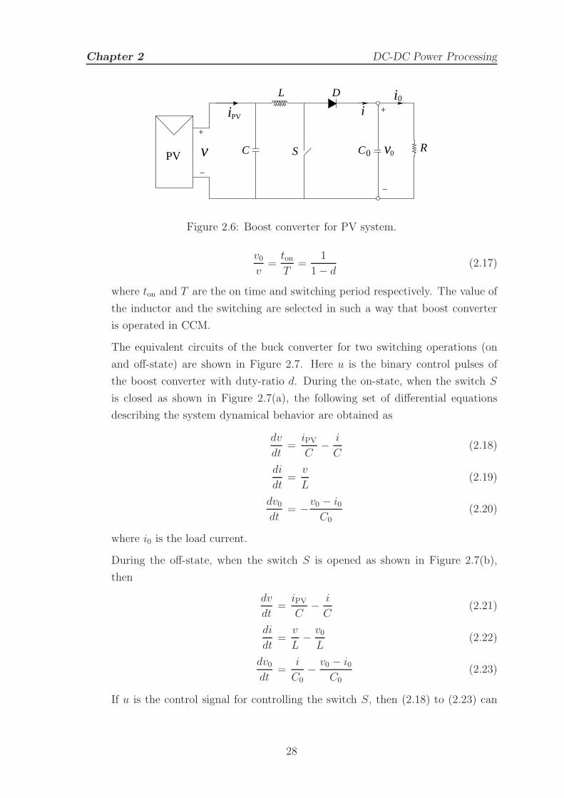
Chapter 2 DC-DC Power Processing
+
−
i
0
+
−
PV
i
C
i
PV C
0
R
DL
S vv 0
Figure 2.6: Boost converter for PV system.
v0v
=tonT
=1
1− d(2.17)
where ton and T are the on time and switching period respectively. The value of
the inductor and the switching are selected in such a way that boost converter
is operated in CCM.
The equivalent circuits of the buck converter for two switching operations (on
and off-state) are shown in Figure 2.7. Here u is the binary control pulses of
the boost converter with duty-ratio d. During the on-state, when the switch S
is closed as shown in Figure 2.7(a), the following set of differential equations
describing the system dynamical behavior are obtained as
dv
dt=
iPVC
− i
C(2.18)
di
dt=
v
L(2.19)
dv0dt
= −v0 − i0C0
(2.20)
where i0 is the load current.
During the off-state, when the switch S is opened as shown in Figure 2.7(b),
then
dv
dt=
iPVC
− i
C(2.21)
di
dt=
v
L− v0
L(2.22)
dv0dt
=i
C0
− v0 − i0C0
(2.23)
If u is the control signal for controlling the switch S, then (2.18) to (2.23) can
28
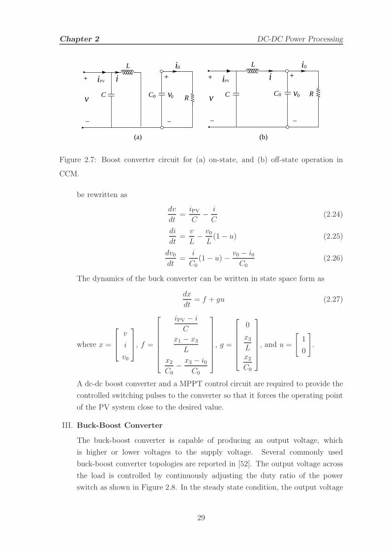
Chapter 2 DC-DC Power Processing
+
−
+
−
v
i
v
L
iPV i0
R0C0C
(a)
+
−
+
−
v
i
L
v R
i
(b)
PVi
C 0C
0
0
Figure 2.7: Boost converter circuit for (a) on-state, and (b) off-state operation in
CCM.
be rewritten as
dv
dt=
iPVC
− i
C(2.24)
di
dt=
v
L− v0
L(1− u) (2.25)
dv0dt
=i
C0
(1− u)− v0 − i0C0
(2.26)
The dynamics of the buck converter can be written in state space form as
dx
dt= f + gu (2.27)
where x =
v
i
v0
, f =
iPV − i
C
x1 − x3
L
x2
C0
− x3 − i0C0
, g =
0
x3
Lx2
C0
, and u =
[
1
0
]
.
A dc-dc boost converter and a MPPT control circuit are required to provide the
controlled switching pulses to the converter so that it forces the operating point
of the PV system close to the desired value.
III. Buck-Boost Converter
The buck-boost converter is capable of producing an output voltage, which
is higher or lower voltages to the supply voltage. Several commonly used
buck-boost converter topologies are reported in [52]. The output voltage across
the load is controlled by continuously adjusting the duty ratio of the power
switch as shown in Figure 2.8. In the steady state condition, the output voltage
29
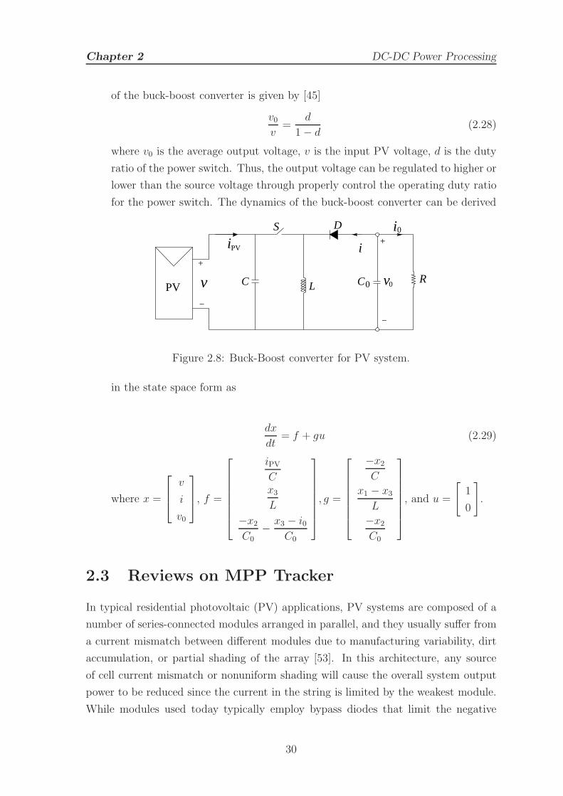
Chapter 2 DC-DC Power Processing
of the buck-boost converter is given by [45]
v0v
=d
1− d(2.28)
where v0 is the average output voltage, v is the input PV voltage, d is the duty
ratio of the power switch. Thus, the output voltage can be regulated to higher or
lower than the source voltage through properly control the operating duty ratio
for the power switch. The dynamics of the buck-boost converter can be derived
+
−
0
+
−
PV
i
Cv
i
PV C
0
R
i
S
L
D
v0
Figure 2.8: Buck-Boost converter for PV system.
in the state space form as
dx
dt= f + gu (2.29)
where x =
v
i
v0
, f =
iPVCx3
L
−x2
C0
− x3 − i0C0
, g =
−x2
C
x1 − x3
L
−x2
C0
, and u =
[
1
0
]
.
2.3 Reviews on MPP Tracker
In typical residential photovoltaic (PV) applications, PV systems are composed of a
number of series-connected modules arranged in parallel, and they usually suffer from
a current mismatch between different modules due to manufacturing variability, dirt
accumulation, or partial shading of the array [53]. In this architecture, any source
of cell current mismatch or nonuniform shading will cause the overall system output
power to be reduced since the current in the string is limited by the weakest module.
While modules used today typically employ bypass diodes that limit the negative
30

Chapter 2 DC-DC Power Processing
effect of partial shading and help protect the panels [54], it is still the case that
shading effect has a significant negative impact on any solar PV installations. The
module-integrated converter (MIC), the so called micro-converter concept has been
exploited to address this problem by operating each module at its unique maximum
power point (MPP) and providing separate dc-dc conversion for each module [55–57].
Through dc-dc converters, localized control of module current and voltage can be
achieved, and each module can operate at its independent MPP to improve the energy
extraction of the overall system.
However, designing a fast and robust PV MPP tracking (MPPT) controller (with
high tracking efficiency) for such MIC is a challenging task for power electronics
practitioners [58]. Over the past decades, many efforts have been devoted to
this research area and reviews are available now on this subject [58–61] and
references therein. In most of cases, investigations are primarily based on standard
P&O algorithms, constant-frequency (CF) pulse-width modulated (PWM) operation,
and small-signal averaging technique or transfer function based stability analysis.
However, averaging is only an approximated procedure to obtain the low-frequency
behavior of the actual switching model of the dc-dc converters. The averaged model
was failed to predict many fast-scale instabilities (e.g., subharmonic oscillations and
chaotic behavior) that may develop in the current and voltage waveform at clock
frequency, causes high conduction loss and excessive switching stress [62]. This
shortcoming is due to elimination of the discontinuous effect of the real converter
system and ignoring the microscopic dynamics inside the switching cycle (see [63]
and refs. therein) as well as the quantization effects [64], which is inherently induced
in all digitally controlled MPPT systems [65]. Because of this approximation, the
traditional use of averaging-based analysis technique and also P&O algorithm cannot
always extract the best optimized performances in terms of fast and robust dynamic
performances, steady-state oscillations, and tracking efficiency. The optimized
performances of P&O based MPPT controller depend largely on amplitude and
frequency of the perturbations applied to the switching converter [66]. It is therefore
necessary to apply a more advanced controller as well as the fast-scale stability analysis
technique (bifurcation analysis) in order to achieve such specific performances.
It has, however, been recently reported that dynamic responses of a MPP tracker
can be improved by combining the different mode of controllers like sliding and
constant-frequency PWM [67] or hysteresis controller [68–71] with relatively costly
A/D and D/A converters. As a consequence of this combination, the sliding-mode
controller (SMC) essentially utilizes a CF-switching (CFS) control law to force the
state trajectory from any initial position onto a specified surface in the state space,
31
Chapter 2 DC-DC Power Processing
called the switching or sliding surface (SS), and maintain it on this surface for
all subsequent time. The main features of the ideal sliding mode (SM) are the
robustness against the parameters fluctuations. Despite these unique advantages of
ideal one, the controllers reported earlier completely rely on smooth averaged models
of the dc-dc switching converters and the control is only valid on a reduced-order
SS. However, in real life power electronics converter systems, SM actually occurs
not on its discontinuity surface, but within the vicinity of that discontinuity or
within a boundary layer surrounded by multiple switching surfaces, like hysteresis
control [68–71]. In such situation, the control components may take up values which
are different from the equivalent control law, therefore, result in a richer set of motions
on the sliding manifold [72]. The existence of a unique sliding motion can only be
determined successfully using the notion of Utkin’s equivalent control or Filippov
continuation method if the fast-scale dynamics is stable. The mathematical proof
of this concept has already been developed earlier in multi-scale hybrid dynamical
systems (HDSs) [73]. Since the switching converters used in PV systems come under
this class of systems [63, 74], the equivalent equation of motion derived from Utkin’s
theory may not be always successful to predict the existence of a unique solution or
robustness. It can only be successfully used when the long-time averaging of fast-scale
oscillations becomes zero, in other words, when the capacitor voltage and the inductor
current waveforms during the steady-state operation are periodic in nature [73].
In view of this, this work proposes a fast and robust analog-MPP tracker [also
called as analog sliding-mode controller (ASMC)] which is implemented and designed
by using the concepts of Utkin’s equivalent control theory and fast-scale stability
analysis. The main objectives of applying such concepts are to provide the control
support for the MPPT system which are required for 1) guaranteed stability with high
robustness against the parameters uncertainties, and 2) fast dynamic responses under
rapidly varying environmental conditions. This cannot be met by conventional digital
or analog MPPT controllers without continuously tuning the controller parameters
and complex controller architecture [58,75]. Thus, the choice of this analog solution is
quite attractive because of its low cost and capability of easy integration with a normal
dc-dc converter in integrated circuit (IC) form, so that plug-and-play operation for
many low power residential PV applications [55,76] can be easily achieved. Moreover,
since the proposed analog controller inherently acts like a CF hysteresis controller [68,
69], it retains all of the properties of an ideal SMC, that is, simplicity in practical
realization, good dynamic response with high robustness, and less overshoot in the
output module voltage. In addition, it provides a relatively larger bandwidth to
eliminate the low-frequency limit cycle oscillation [65], and reduces the cross-coupling
32
Chapter 2 DC-DC Power Processing
effects which is normally occurred in series-connected converters systems [77].
2.4 Module-Integrated Analog MPP Trackers
In this section, the architecture shown in Figure 2.9 is considered in order to introduce
the proposed modular MPP trackers. It consists of two PV modules which are
interconnected with two nonautonomous switching converters, and each of them
comprising of an input capacitor C, a low-pass filter with inductor L and capacitor
Co, a diode D, and a controllable switch S, governed by an analog MPPT controller
without imposing any external control or perturbation. The output of the dc-dc
converters are connected in series and put in parallel to dc bus (input of a dc-ac
converter), represented by means of a Thevenin model [70, 78]. Mathematically, the
output voltage Vbus and corresponding throughput power Po of such series-connected
converters system can be expressed as a sum of all modular MPPT controllers [56,79],
such that
Vbus ≈2∑
k=1
vko and Po = io
2∑
k=1
vko ; since Req ≈ 0. (2.30)
Here io is the averaged load current and vko is the output voltage of the k-th dc-dc
converter, which is dynamically coupled with other converters’ output voltage. In
a system like (2.30), every disturbance induced on the output voltage, by the other
MPVSs and/or by the inverter, directly propagates on the modules’ output voltage.
This may lead to instability or dynamic performance degradation [77,79,80]. In [80],
authors demonstrated that if the MPPT controller is fast enough, any disturbances
in the closed-loop system do not significantly affect the operation of a single MPVS.
This is also true for inverter system. Since fast controller with larger loop-gain has
better output disturbance rejection capability than that of slower one [81], therefore
it can avoid the propagation of low frequency perturbation to the PV module side (see
ref. [82]). However, this mandatory requirement makes the achievement of a fast and
stable controlled converter system (in terms of fast- and slow-scale stability) which is
really a difficult task.
This paper thus promises to deal the complete stability analysis of proposed analog
MPVS in order to achieve fast and robust dynamic responses. The system under this
control logic is excellent in tracking effectiveness and rapid dynamic responses [83].
In addition, it inherently makes the MPP as an attractor of the system. Irrespective
of any initial voltage, the controller always forces the system’s state trajectories to
33
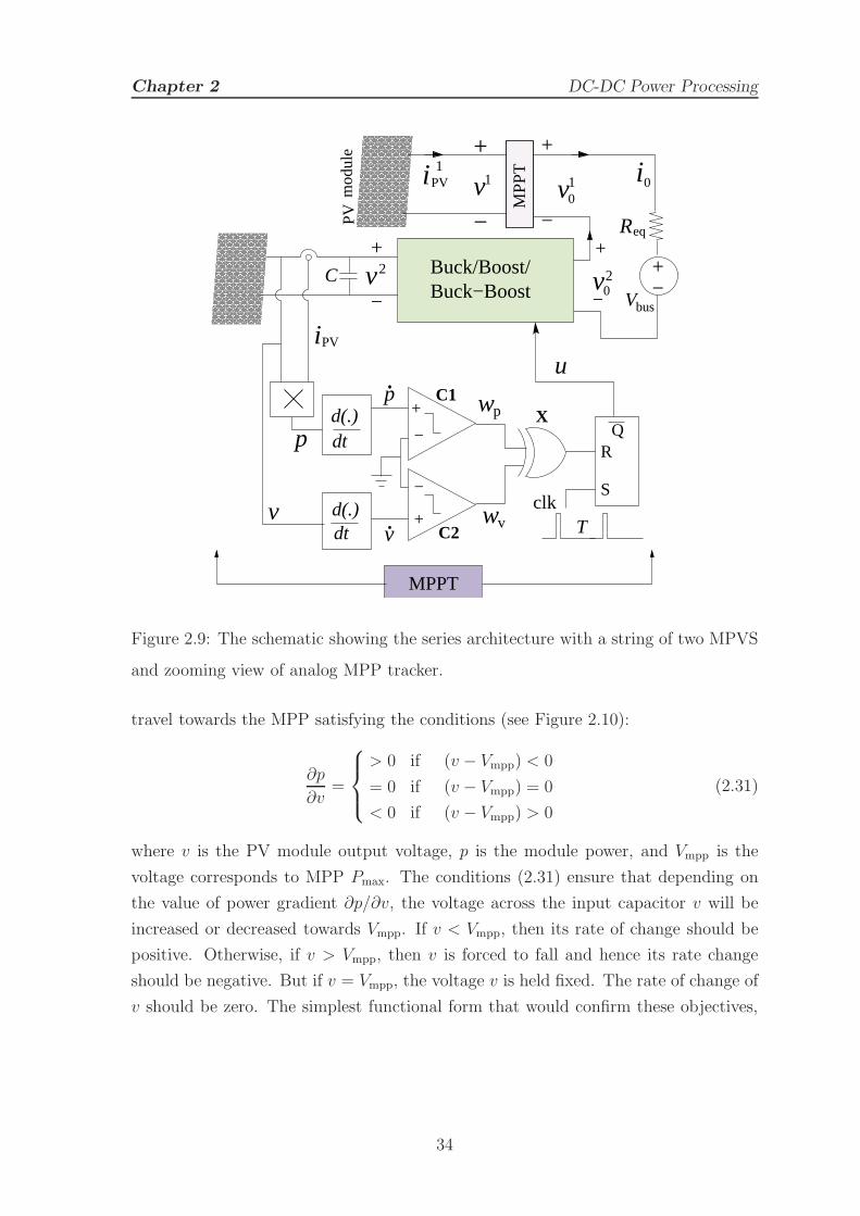
Chapter 2 DC-DC Power Processing
pd(.)dt
d(.)dt
1v 0i
Req
1v0
busV
PV
mod
ule
v
w
wC2
clkT
−
+
+
−
C1X
v
p
i
p
v
u
C +−
+
−
PV1i
2v−
++
−
+
−
v02
PV
MP
PT
QR
S
MPPT
Buck−BoostBuck/Boost/
Figure 2.9: The schematic showing the series architecture with a string of two MPVS
and zooming view of analog MPP tracker.
travel towards the MPP satisfying the conditions (see Figure 2.10):
∂p
∂v=
> 0 if (v − Vmpp) < 0
= 0 if (v − Vmpp) = 0
< 0 if (v − Vmpp) > 0
(2.31)
where v is the PV module output voltage, p is the module power, and Vmpp is the
voltage corresponds to MPP Pmax. The conditions (2.31) ensure that depending on
the value of power gradient ∂p/∂v, the voltage across the input capacitor v will be
increased or decreased towards Vmpp. If v < Vmpp, then its rate of change should be
positive. Otherwise, if v > Vmpp, then v is forced to fall and hence its rate change
should be negative. But if v = Vmpp, the voltage v is held fixed. The rate of change of
v should be zero. The simplest functional form that would confirm these objectives,
34

Chapter 2 DC-DC Power Processing
i.e.,
dv
dt=
> 0 if (v − Vmpp) < 0
= 0 if (v − Vmpp) = 0
< 0 if (v − Vmpp) > 0
(2.32)
can be expressed in terms of dv/dt as,
dv
dt= −γ(v − Vmpp) (2.33)
where γ is the positive number associated with dynamic response of the controller [83];
the larger the γ, the faster the dynamic response 1. The graphical representation of
(2.33) is shown in Figure 2.10. It is observed that because (2.31) and (2.32) have
similar forms, a simple control law can be deducted by making
dp
dt=
∂p
∂v
dv
dt(2.34)
v ∝ ∂p
∂v= α
∂p
∂v(2.35)
where α > 0 is a constant. Now, after substituting (2.34) into expression (2.35) and
using the switching logic (2.31) and (2.32), one can easily obtain the control law and
the control algorithm which are given by
∂p
∂v= p/v (2.36)
v = αp/∂p
∂v(2.37)
= αp/v
In practice, realization of such an algorithm v = αp/v is slightly difficult due to
presence of an algebraic loop. Since v appears on both sides, it would manifest
high frequency oscillation. One requires an analog divider circuit which is again
undesirable. Moreover, divider circuit causes many other imperfect operations and
even singularity problem when v becomes zero (in this case, it happens only when
v = Vmpp). While by rearranging the desired control algorithm into the form v2 = αp
does not help either. In fact, squaring of v not only destroys the vital information of
its sign, but also causes the singularity problem at MPP. In [83], authors showed that
the problem of singularity can be resolved by redefining the above control law (2.36)
1However, any function complying with (2.32) would fulfill the objective of (2.31) and (2.32),
which are indeed in similar forms.
35

Chapter 2 DC-DC Power Processing
Vmpp
δδ p
< 0v
δδ pv
> 0δδ p
=0v
dtv
d
v0
p,
Eq.(4)
γ
MPP
Figure 2.10: The representative characteristics of v making Vmpp as an attractor.
as
∂p
∂v:= sign(p/v) ≡
sign(p)
sign(v)≡ sign(p)sign(v) (2.38)
⇒ sign(v) = sign(H) =
+1 if H < 0
−1 if H > 0.(2.39)
Here, the expressions (2.38)-(2.39) indicate that in-spite of zero-division the nonlinear
function sign(.)/sign(.) can be reformulated as a function of multiplication G(.) =
sign(.)sign(.) which are realized by a couple of comparators C1, C2 followed by an
exclusive-OR gate X [see Figure 2.9]. The comparators are used to evaluate the sign
of G(.) by producing binary signals (wp, wv) whose value is 0 if p < 0 or 1 if p > 0;
or, 0 if v < 0 or 1 if v > 0. Multiplication of these binary signals using X-OR gate
is further used to generate required switching signals of the control law (2.39). It
essentially contains the information whether v should be increased or decreased to
approach MPP. Since sign(.) function in (2.39) has a discontinuity at the MPP, one
cannot expect an equilibrium point at steady-state, rather the system dynamics is
governed by very high switching frequency. This results in excessive switching losses
and also reduces the life-time of the semiconductor devices.
Although such high switchings can be easily restricted by incorporating latch
circuit into the controller, but its presence makes single discontinuity switching surface
H into a CFS ∆-neighborhood chatter box, or switching box SB=v :Vmpp−∆≤v<
Vmpp+∆; t < T,∆ > 0, surrounded by multiple SSs H = (v−Vmpp) and external clock
pulse having time period T . The switching flow diagram of such control algorithm is
shown in Figure 2.11. It represents that depending on the initial value of the input
capacitor voltage v(0), MIC may operate into two modes: one when v is outside the
36
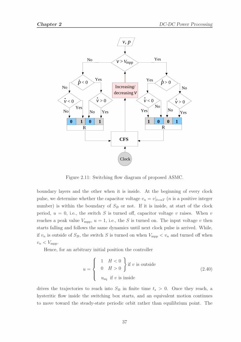
Chapter 2 DC-DC Power Processing
v>Vmpp
p> 0
v < 0 v > 0
p< 0
v < 0 v > 0
Yes
No
Yes
No
NoYes
No Yes Yes Yes
NoNo
R R
v, p
No Yes
1
Clock
Increasing/decreasingv
CFS
0 1 0 1 1 0 0
Figure 2.11: Switching flow diagram of proposed ASMC.
boundary layers and the other when it is inside. At the beginning of every clock
pulse, we determine whether the capacitor voltage vn = v|t=nT (n is a positive integer
number) is within the boundary of SB or not. If it is inside, at start of the clock
period, u = 0, i.e., the switch S is turned off, capacitor voltage v raises. When v
reaches a peak value Vmpp, u = 1, i.e., the S is turned on. The input voltage v then
starts falling and follows the same dynamics until next clock pulse is arrived. While,
if vn is outside of SB, the switch S is turned on when Vmpp < vn and turned off when
vn < Vmpp.
Hence, for an arbitrary initial position the controller
u =
1 H < 0
0 H > 0
if v is outside
ueq if v is inside
(2.40)
drives the trajectories to reach into SB in finite time ts > 0. Once they reach, a
hysteritic flow inside the switching box starts, and an equivalent motion continues
to move toward the steady-state periodic orbit rather than equilibrium point. The
37
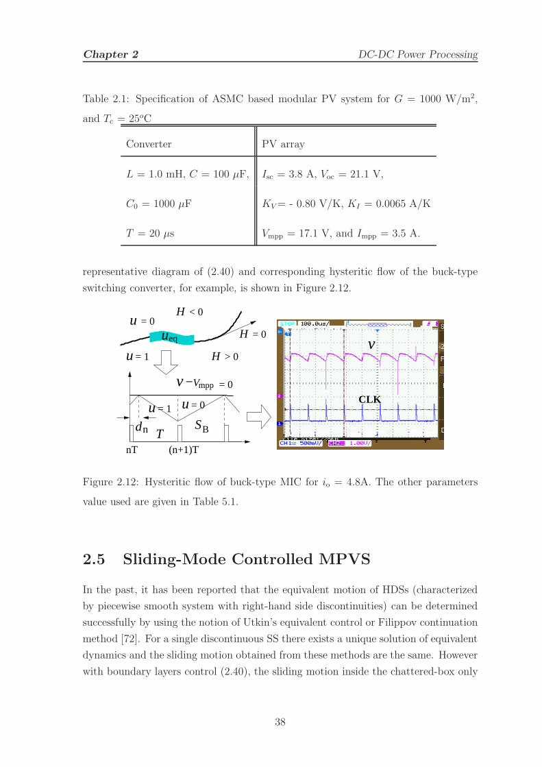
Chapter 2 DC-DC Power Processing
Table 2.1: Specification of ASMC based modular PV system for G = 1000 W/m2,
and Tc = 25oC
Converter PV array
L = 1.0 mH, C = 100 µF, Isc = 3.8 A, Voc = 21.1 V,
C0 = 1000 µF KV= - 0.80 V/K, KI = 0.0065 A/K
T = 20 µs Vmpp = 17.1 V, and Impp = 3.5 A.
representative diagram of (2.40) and corresponding hysteritic flow of the buck-type
switching converter, for example, is shown in Figure 2.12.
= 1
H < 0
H > 0
= 0
H = 0
dn
= 1
−
BS
Vmpp = 0
= 0
nT (n+1)T
u
uu
u
vCLK
T
vueq
Figure 2.12: Hysteritic flow of buck-type MIC for io = 4.8A. The other parameters
value used are given in Table 5.1.
2.5 Sliding-Mode Controlled MPVS
In the past, it has been reported that the equivalent motion of HDSs (characterized
by piecewise smooth system with right-hand side discontinuities) can be determined
successfully by using the notion of Utkin’s equivalent control or Filippov continuation
method [72]. For a single discontinuous SS there exists a unique solution of equivalent
dynamics and the sliding motion obtained from these methods are the same. However
with boundary layers control (2.40), the sliding motion inside the chattered-box only
38
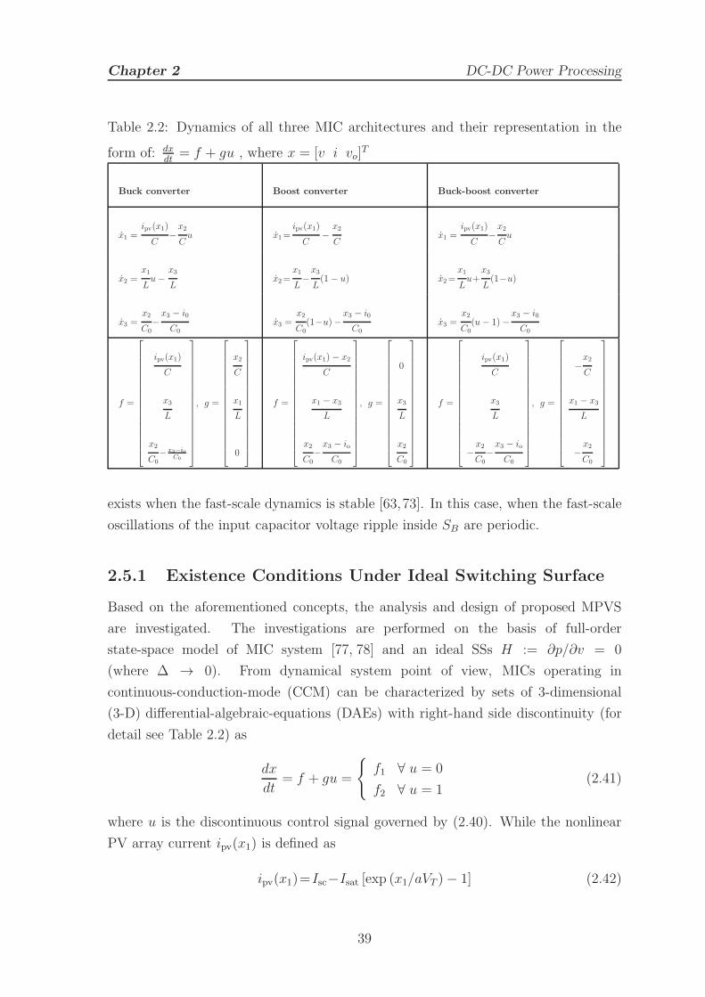
Chapter 2 DC-DC Power Processing
Table 2.2: Dynamics of all three MIC architectures and their representation in the
form of: dxdt
= f + gu , where x = [v i vo]T
Buck converter Boost converter Buck-boost converter
x1 =ipv(x1)
C−x2
Cu x1=
ipv(x1)
C−
x2
Cx1 =
ipv(x1)
C−x2
Cu
x2 =x1
Lu−
x3
Lx2=
x1
L−x3
L(1− u) x2=
x1
Lu+
x3
L(1−u)
x3 =x2
C0−x3 − i0
C0x3 =
x2
C0(1−u)−
x3 − i0
C0x3 =
x2
C0(u− 1)−
x3 − i0
C0
f =
ipv(x1)
C
x3
L
x2
C0− x3−io
C0
, g =
x2
C
x1
L
0
f =
ipv(x1)− x2
C
x1 − x3
L
x2
C0−x3 − io
C0
, g =
0
x3
L
x2
C0
f =
ipv(x1)
C
x3
L
−x2
C0−x3 − io
C0
, g =
−x2
C
x1 − x3
L
−x2
C0
exists when the fast-scale dynamics is stable [63,73]. In this case, when the fast-scale
oscillations of the input capacitor voltage ripple inside SB are periodic.
2.5.1 Existence Conditions Under Ideal Switching Surface
Based on the aforementioned concepts, the analysis and design of proposed MPVS
are investigated. The investigations are performed on the basis of full-order
state-space model of MIC system [77, 78] and an ideal SSs H := ∂p/∂v = 0
(where ∆ → 0). From dynamical system point of view, MICs operating in
continuous-conduction-mode (CCM) can be characterized by sets of 3-dimensional
(3-D) differential-algebraic-equations (DAEs) with right-hand side discontinuity (for
detail see Table 2.2) as
dx
dt= f + gu =
f1 ∀ u = 0
f2 ∀ u = 1(2.41)
where u is the discontinuous control signal governed by (2.40). While the nonlinear
PV array current ipv(x1) is defined as
ipv(x1)=Isc−Isat [exp (x1/aVT )− 1] (2.42)
39
Chapter 2 DC-DC Power Processing
with panel saturation and short-circuit current Isat and Isc, diode ideality constant a,
and thermal voltage VT with series and parallel resistance rs ≈ 0, rp ≈ ∞, respectively.
Having obtained the system description (2.41), next step is to design the controller,
so that, control law u will direct the state trajectory towards the desired operation.
In this case, it is appropriate to have a SMC law (2.40) that will adopt the switching
function H , defined by
H :=∂p
∂x1
= ipv(x1)−x1IsataVT
exp
(x1
aVT
)
= 0. (2.43)
The objective is that, from any arbitrary initial position x(0), it will drive the system
trajectory on either side of the SS H = 0. The trajectory is said to be in sliding
mode if the motion within the vicinity of H is maintained and consequently directed
towards the steady-state equilibrium point. In other words, it can also be stated
that SMC is performing its control decision by utilizing the sliding plane H = 0
as a reference path, on which trajectory will be attracted and eventually converged
towards the equilibrium to achieve the desired steady-state operation satisfying the
inequality conditions:
limH→0+
dH
dt< 0, and lim
H→0−
dH
dt> 0. (2.44)
The conditions (2.44) are known as the SM reachability or existence conditions [69,84].
For an ideal SM-controlled MICs, these conditions can be easily derived from the time
derivative of SS dHdt
= ∇H dxdt
and then substituting this value into (2.44). From (2.43),
∇H can be evaluated as
∇H=
[
x1∂2ipv∂x2
1
+2∂ipv∂x1
0 0
]
= [F (x1) 0 0]
where
F (x1) =
[
−Isat(2aVT + x1)
(aVT )2exp
(x1
aVT
)
0 0
]
is only a function of PV module voltage with nonzero steady-state value. Substituting
it into (2.44), and using (2.41) and (2.43) one can easily obtain the boundary
conditions for both buck and buck-boost converters as
Π1 := ipv − x2 < 0; and Π2 := ipv > 0. (2.45)
While for boost converter, it can be obtained as
Π1 := ipv − x2 < 0; and Π2 := ipv − x2 > 0. (2.46)
The conditions (2.45)-(2.46) are essentially interpreted as a region, requirement
for the system trajectories to be oriented towards the sliding surface H from both
40
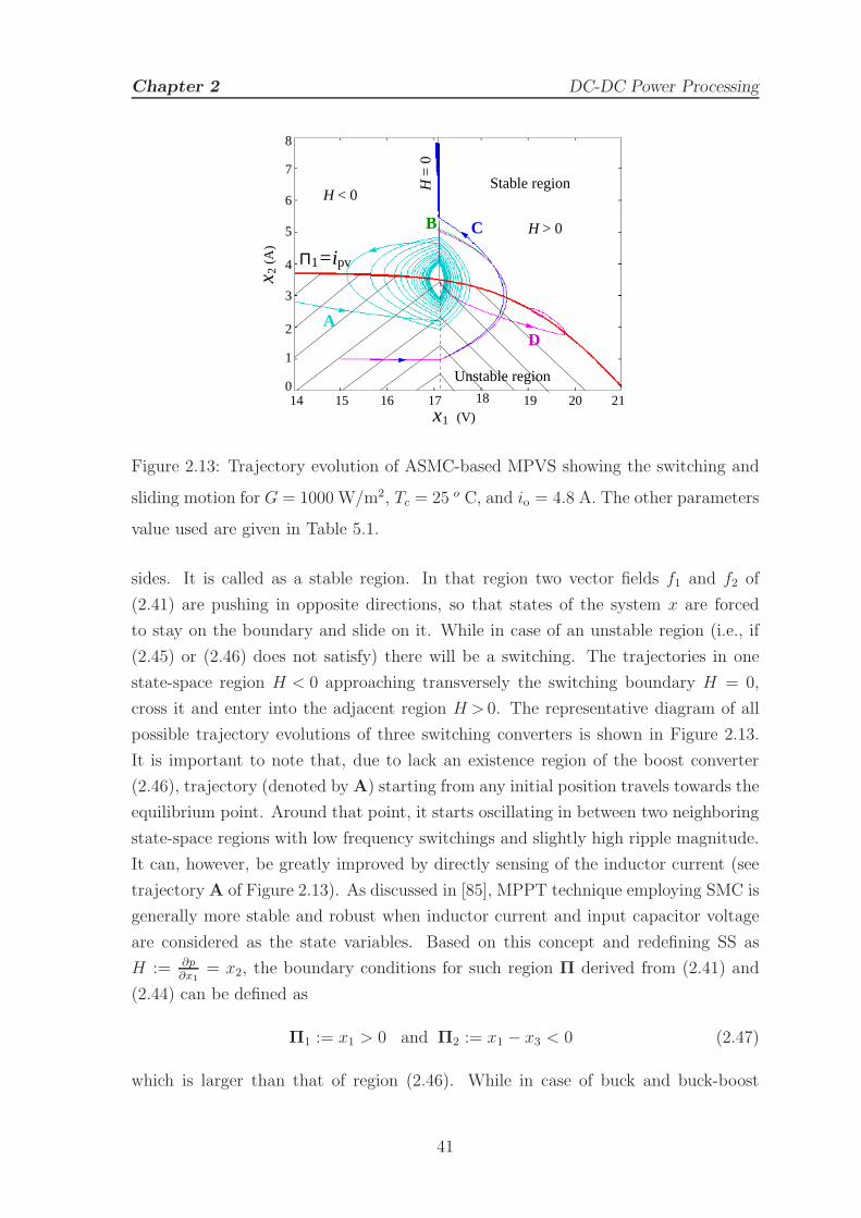
Chapter 2 DC-DC Power Processing
1
2
H > 0
H < 0
3
H
15 16 17 18 19 2014 21
4
8
7
6
5
2
0
1
= 0
x (V)
x(A
)
Stable region
Unstable region
=i pv
B C
AD
1Π
Figure 2.13: Trajectory evolution of ASMC-based MPVS showing the switching and
sliding motion for G = 1000 W/m2, Tc = 25 o C, and io = 4.8 A. The other parameters
value used are given in Table 5.1.
sides. It is called as a stable region. In that region two vector fields f1 and f2 of
(2.41) are pushing in opposite directions, so that states of the system x are forced
to stay on the boundary and slide on it. While in case of an unstable region (i.e., if
(2.45) or (2.46) does not satisfy) there will be a switching. The trajectories in one
state-space region H < 0 approaching transversely the switching boundary H = 0,
cross it and enter into the adjacent region H > 0. The representative diagram of all
possible trajectory evolutions of three switching converters is shown in Figure 2.13.
It is important to note that, due to lack an existence region of the boost converter
(2.46), trajectory (denoted by A) starting from any initial position travels towards the
equilibrium point. Around that point, it starts oscillating in between two neighboring
state-space regions with low frequency switchings and slightly high ripple magnitude.
It can, however, be greatly improved by directly sensing of the inductor current (see
trajectoryA of Figure 2.13). As discussed in [85], MPPT technique employing SMC is
generally more stable and robust when inductor current and input capacitor voltage
are considered as the state variables. Based on this concept and redefining SS as
H := ∂p∂x1
= x2, the boundary conditions for such region Π derived from (2.41) and
(2.44) can be defined as
Π1 := x1 > 0 and Π2 := x1 − x3 < 0 (2.47)
which is larger than that of region (2.46). While in case of buck and buck-boost
41
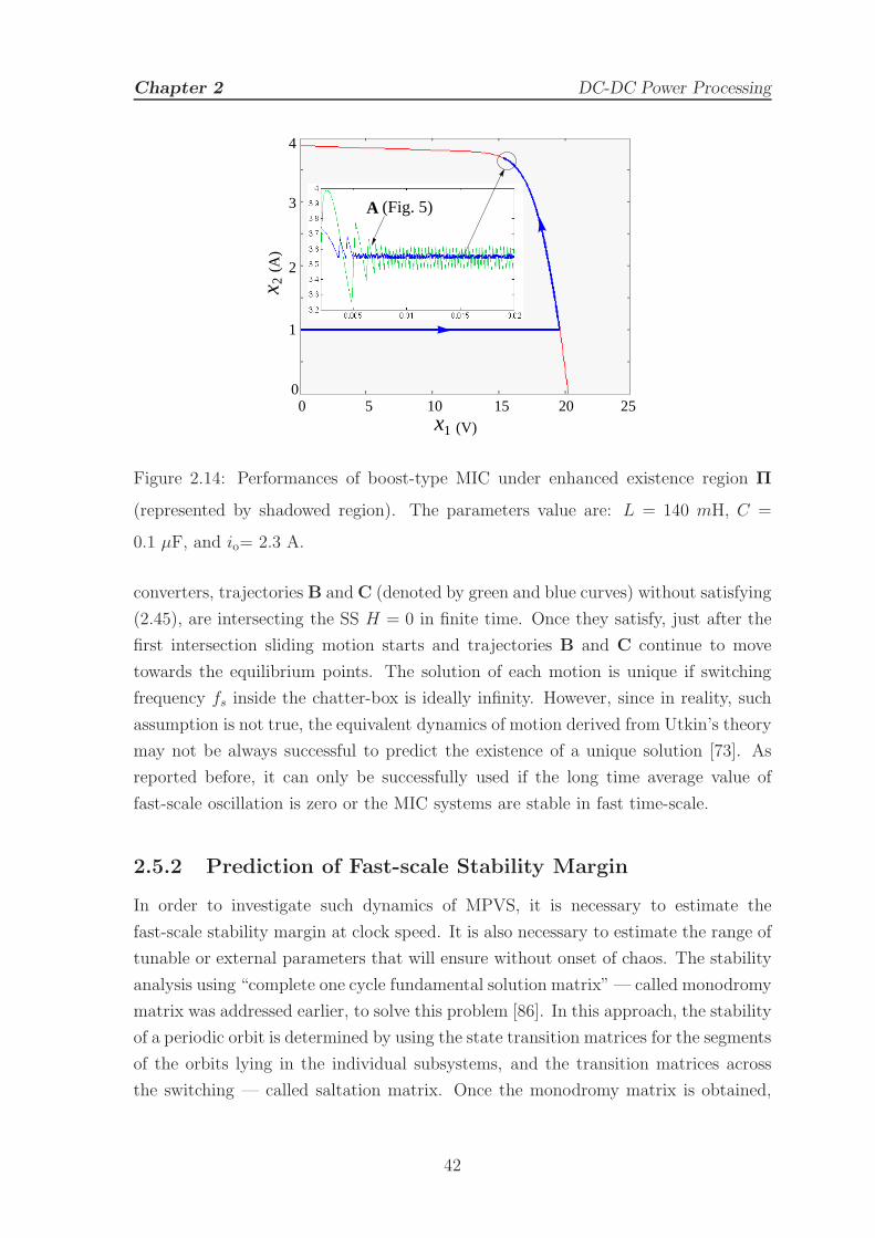
Chapter 2 DC-DC Power Processing
0 252015105
4
3
2
1
0
1 (V)x
2(A
)x
A (Fig. 5)
Figure 2.14: Performances of boost-type MIC under enhanced existence region Π
(represented by shadowed region). The parameters value are: L = 140 mH, C =
0.1 µF, and io= 2.3 A.
converters, trajectories B andC (denoted by green and blue curves) without satisfying
(2.45), are intersecting the SS H = 0 in finite time. Once they satisfy, just after the
first intersection sliding motion starts and trajectories B and C continue to move
towards the equilibrium points. The solution of each motion is unique if switching
frequency fs inside the chatter-box is ideally infinity. However, since in reality, such
assumption is not true, the equivalent dynamics of motion derived from Utkin’s theory
may not be always successful to predict the existence of a unique solution [73]. As
reported before, it can only be successfully used if the long time average value of
fast-scale oscillation is zero or the MIC systems are stable in fast time-scale.
2.5.2 Prediction of Fast-scale Stability Margin
In order to investigate such dynamics of MPVS, it is necessary to estimate the
fast-scale stability margin at clock speed. It is also necessary to estimate the range of
tunable or external parameters that will ensure without onset of chaos. The stability
analysis using “complete one cycle fundamental solution matrix” — called monodromy
matrix was addressed earlier, to solve this problem [86]. In this approach, the stability
of a periodic orbit is determined by using the state transition matrices for the segments
of the orbits lying in the individual subsystems, and the transition matrices across
the switching — called saltation matrix. Once the monodromy matrix is obtained,
42

Chapter 2 DC-DC Power Processing
the eigenvalues of that matrix determine the stability of the periodic orbit to small
perturbation.
To apply this concept, we derive an approximate chattered dynamics inside the
switching box SB by successively linearizing (2.42) around the MPP as
ipv = Impp − β (x1 − Vmpp) (2.48)
and
β =dipvdx1
|x1=Vmpp≈ Impp
Vmpp(2.49)
And then, substituting it into (2.41) to form a set of 2-D linear time-invariant (LTI)
subsystems 2 as
dx
dt=
M1 : A1x+B1 ∀ nT <t<dnT + nT
M2 : A2x+B2 ∀ dnT + nT <t< (1+n)T(2.50)
where dn is the steady-state duty ratio (see Figure 2.12), and Ai and Bi are the
corresponding system and input matrices respectively, as shown in Table 2.3. Having
obtained (2.50) if one assumes t = nT is a switching instant, then the monodromy
matrix over complete one cycle T can be expressed as the composition of state
transition matrices over the two phases of evolutions M1 and M2, and two saltation
matrices for the switching from M1 to M2(S1) and back to M1(S2) as [86]:
M = S2Φ2S1Φ1 (2.51)
where Φ1 = eA1dnT and Φ2 = eA1(1−dn)T are the state transition matrices. S1 and S2
are the saltation matrices represented by
S1 = I+[(A2 − A1)x+ (B2 −B1)]∇H
∇H(A1x+B1) +dHdt
∣∣∣∣∣t=dnT
, (2.52)
and S2 = I, an identity matrix. However, to evaluate such matrices one needs
to know the duty ratio d and corresponding state vectors at the switching instant
t∗ = dnT . This can be accurately obtained by using the Newton-Raphson method.
Alternatively one can use any standard simulator to obtain the stable behavior,
from which the information about both dn and x∗|t=dnT can be extracted. However,
2Since in local neighborhood of MPP the chattered dynamics is much faster than x3, it is therefore
reasonable to consider x3 = Vo and dx3/dt = 0.
43
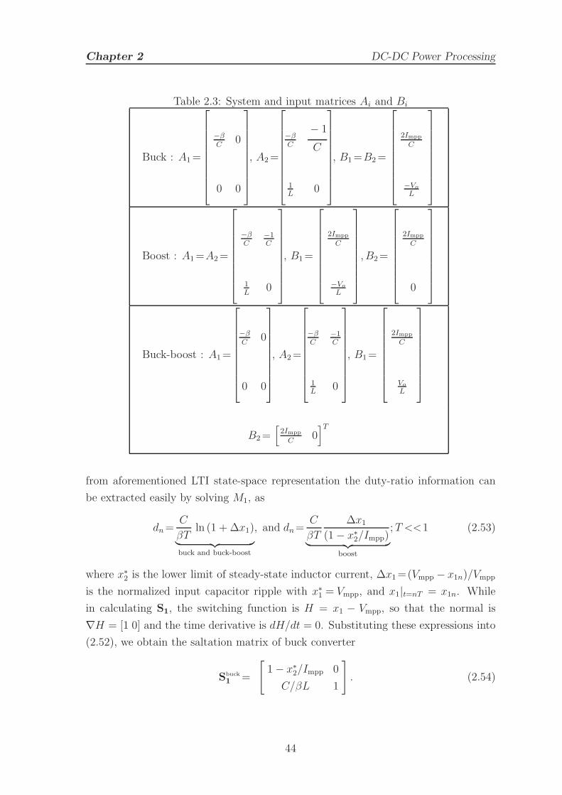
Chapter 2 DC-DC Power Processing
Table 2.3: System and input matrices Ai and Bi
Buck : A1=
−βC
0
0 0
, A2=
−βC
− 1
C
1L
0
, B1=B2=
2Impp
C
−Vo
L
Boost : A1=A2=
−βC
−1C
1L
0
, B1=
2Impp
C
−Vo
L
,B2=
2Impp
C
0
Buck-boost : A1=
−βC
0
0 0
, A2=
−βC
−1C
1L
0
, B1=
2Impp
C
Vo
L
B2=[2Impp
C0]T
from aforementioned LTI state-space representation the duty-ratio information can
be extracted easily by solving M1, as
dn=C
βTln (1 + ∆x1)
︸ ︷︷ ︸
buck and buck-boost
, and dn=C
βT
∆x1
(1− x∗
2/Impp)︸ ︷︷ ︸
boost
;T <<1 (2.53)
where x∗
2 is the lower limit of steady-state inductor current, ∆x1=(Vmpp − x1n)/Vmpp
is the normalized input capacitor ripple with x∗
1 = Vmpp, and x1|t=nT = x1n. While
in calculating S1, the switching function is H = x1 − Vmpp, so that the normal is
∇H = [1 0] and the time derivative is dH/dt = 0. Substituting these expressions into
(2.52), we obtain the saltation matrix of buck converter
Sbuck
1=
[
1− x∗
2/Impp 0
C/βL 1
]
. (2.54)
44
Chapter 2 DC-DC Power Processing
Similarly, for boost and buck-boost converters it can be easily evaluated as
Sboost
1=
[
1 0
0 1/(1−D)
]
(2.55)
and
Sbuck-boost
1=
[
1− x∗
2/Impp 0
C(1−D)/βL 1
]
(2.56)
where D = V0/Vmpp. Once the salutation matrix and corresponding duty-ratios are
known, one can easily calculate the monodromy matrix from (2.51). The monodromy
matrix represents the linearized system integrated around the periodic orbits and
hence, its eigenvalues
λ1,2 = ||M|| (2.57)
represent the Floquet multipliers. If they lie within the unit circle (i.e., λ1,2 < 1), the
orbit is stable and that can be ensured as follows.
2.5.3 Design Guidelines
Here ∆x1 and β are the known parameters and their exact values can be substituted
directly into (2.53) for inspection. However, for designing the circuit parameters
such as C, L, and T , it is necessary to consider their maximum or minimum values
for ensuring the abidance of nominal period-1 operation. Since at nominal operation
∆x1 << 1 is always held, therefore baseline design guideline for choosing such C and T
should be C/βT >> 1, preferably be in the hundred. However T should not be chosen
too high to avoid undesirable high frequency artifacts such as switching noise that may
cause interfere with controller. In such situation, C may be used in conjunction with
T to achieve a large value of C/βT , so that the condition dn := CβT
ln (1 + ∆x1) < 1 is
satisfied. While in case of L, one should choose its value sufficiently large in order to
ensure the CCM operation (i.e., x∗
2 > 0) and the stability condition (2.57). Based on
the above guidelines, we select all the components value and investigate the dynamic
behavior of the MIC by calculating dn and S1, thereby the λ1,2 of the monodromy
matrix. It is found that (say, for buck converter) dn just before the instability at
T ≈ 59 µs is 0.3711, and corresponding eigenvalues are −0.9941 and 0.3692 —
implies the orbit is stable, and that is closely matched with the numerically obtained
bifurcation diagram as shown in Figure 2.15. It also shows that for a low value of
T , the system exhibits stable period-1 orbit. However, as the value of T increases,
it becomes unstable at T ≈ 60µs through a smooth period-doubling bifurcation. For
45
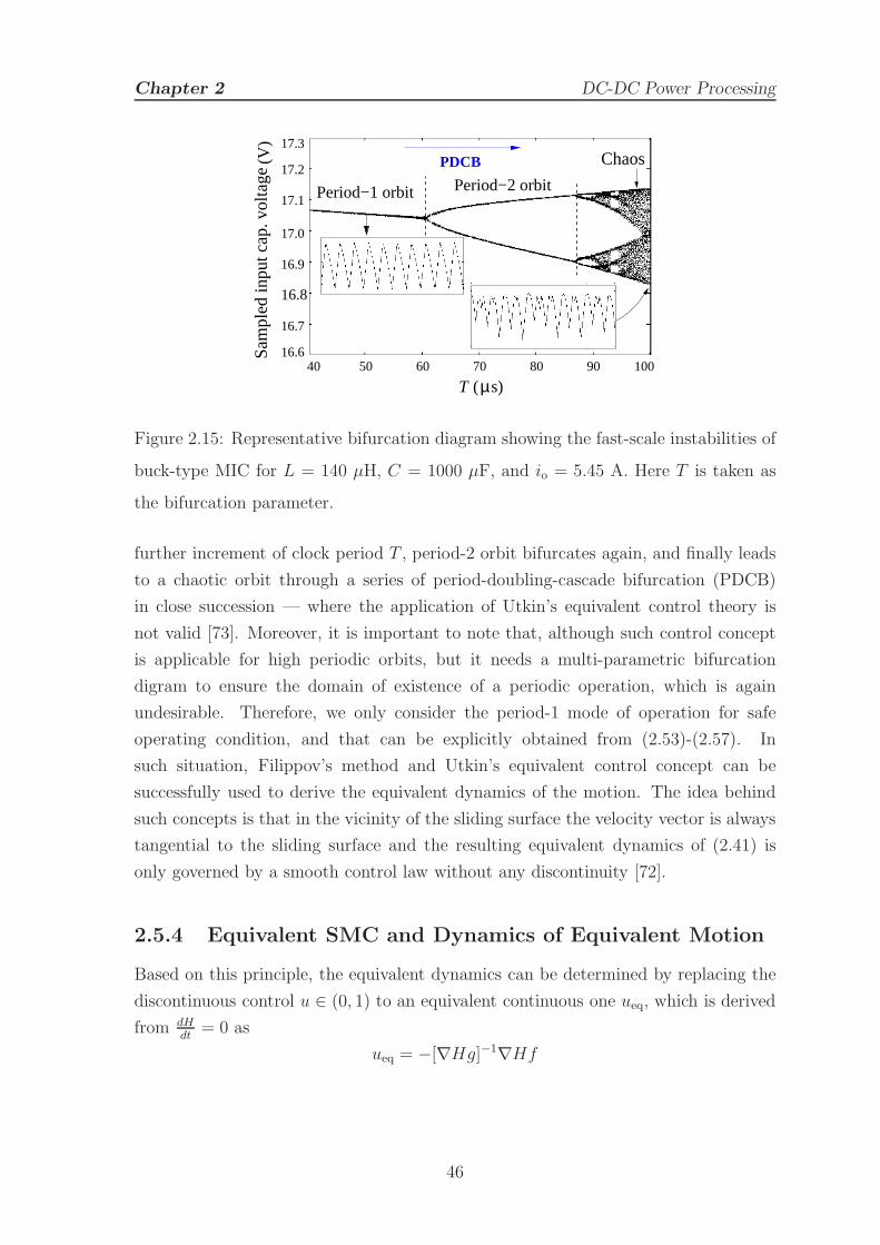
Chapter 2 DC-DC Power Processing
T
16.7
16.640 50 60 70 80 90 100
17.3
17.2
17.1
17.0
16.9
16.8
(V)
µ
Sam
pled
inpu
t cap
. vol
tage
( s)
Chaos
Period−2 orbitPeriod−1 orbit
PDCB
Figure 2.15: Representative bifurcation diagram showing the fast-scale instabilities of
buck-type MIC for L = 140 µH, C = 1000 µF, and io = 5.45 A. Here T is taken as
the bifurcation parameter.
further increment of clock period T , period-2 orbit bifurcates again, and finally leads
to a chaotic orbit through a series of period-doubling-cascade bifurcation (PDCB)
in close succession — where the application of Utkin’s equivalent control theory is
not valid [73]. Moreover, it is important to note that, although such control concept
is applicable for high periodic orbits, but it needs a multi-parametric bifurcation
digram to ensure the domain of existence of a periodic operation, which is again
undesirable. Therefore, we only consider the period-1 mode of operation for safe
operating condition, and that can be explicitly obtained from (2.53)-(2.57). In
such situation, Filippov’s method and Utkin’s equivalent control concept can be
successfully used to derive the equivalent dynamics of the motion. The idea behind
such concepts is that in the vicinity of the sliding surface the velocity vector is always
tangential to the sliding surface and the resulting equivalent dynamics of (2.41) is
only governed by a smooth control law without any discontinuity [72].
2.5.4 Equivalent SMC and Dynamics of Equivalent Motion
Based on this principle, the equivalent dynamics can be determined by replacing the
discontinuous control u ∈ (0, 1) to an equivalent continuous one ueq, which is derived
from dHdt
= 0 as
ueq = −[∇Hg]−1∇Hf
46
Chapter 2 DC-DC Power Processing
where ∇Hg is the nonsingular square matrix. After substituting ueq into (2.41), the
equivalent dynamics of buck, boost, and buck-boost converters are obtained as
dx
dt=
[
0x1ipv−x2x3
x2L
x2 − i0
Co
]T
[
ipv − x2
C0
x1x2 − x3io
x3Co
]T
[
0ipv(x1−x3)
x2L+x3
L
ipv−x2 − i0
Co
]T
(2.58)
which is a nonlinear function of x1. Once there is a nonlinearity, there may exist more
number of feasible equilibrium points and system may converge to some undesirable
operating points. For example, see curve D of Figure 2.13. Theoretically, such
equilibrium points and their domain of attractions could be successfully eliminated
by properly designing the MPVSs, and also identifying their stable operating regions
using stable- and unstable manifolds-based large-signal stability analysis [87]. This
paper however deals to design the system by satisfying existence condition (2.45).
It is found that if the equivalent sliding motion inside the stable region, does not
cross the limiting boundary Π1 = ipv as t → ∞ (i.e., if the existence condition is
not violated), then the system is stable. This can occur only when inductor current
x2 (for buck converter load current io) becomes just greater than that of the MPP
current Impp = ipv|mpp, i.e.,
Π : x2 ≥ Impp. (2.59)
The condition (2.59) is quite general and true for all switching converters, when
there exists a finite existence region defined by (2.45) and (2.46). However, due to
different converters’ topological configurations and switching function formulation,
the stability region satisfying the aforementioned existence condition may also vary.
For instance, the buck converters are conditionally stable and that stability region
(also called MPP region [56]) is strongly limited by their minimum loading condition
Io = Impp. This can also be verified by solving (2.58) as (X2/ipv) |mpp=(X1/X3)>Impp,
where X = [X1 X2 X3]T are steady-state equilibrium point. Although such limitation
can be solved by using buck-boost converters (since Impp <X2 := (1−X1/X3) ipv <
Impp), but they requires extra hardware circuitries to invert their output voltages.
While the main disadvantages of noninverting buck-boost topology are the increased
number of controllable switches and inductors [56], more complex control solution [71],
and the achievable conversion efficiency, which is typically lower than the buck or boost
converter for the same rating. In contrast, the boost converter is an attractive choice
47
Chapter 2 DC-DC Power Processing
because of its ability to increase the output voltage (requiring fewer panels for a given
desired output voltage), but main disadvantage is its limited operating region. The
output current of boost converter can never be higher than the input current, the
range over which current mismatch can be addressed is severely limited [53, 55, 88].
Regardless of the control algorithms used it is always true for boost converters, and it
can also be easily validated from reduced-order dynamics (2.58) as X2=(X3/X1)Io≤Io, where X2|mpp :=Impp.
Therefore, it can be concluded that the aforementioned concepts provide a simple
way for the circuit designer to select the parameters for successful operation of ASMC.
Given certain specifications, the designer would first roughly set the range of circuit
parameters and load in a conventional way based on (2.58). This gives the desired
slow time-scale stability and transient performance, but will not guarantee that the
system will be stable on a fast time-scale. In order to ensure the nominal period-1
operation, it will be necessary to calculate the range of storage elements and switching
frequency for which the period-1 orbit will remain stable. The designer will have to
ensure that the circuit parameters simultaneously satisfy the conditions (2.57) and
(2.59). Once it is satisfied, the equivalent motion (2.58) always exists and solution of
that motion is unique.
2.6 Performance Analysis and Its Experimental
Validation
2.6.1 Realization of ASMC-Based MPPT
To investigate the effectiveness in terms of efficiency and dynamic performances, the
concept has been analyzed numerically as well as experimentally (see Figure 2.16
and 2.17) using buck-type MIC. The synchronous buck topology enables both high
switching frequency (important for low cost, small size) and high efficiency, it does not
contribute any voltage gain (which would reduce the number of panels that must be
series connected). In most utility-based and residential installations, however, there
are a sufficient number of PV panels to provide for the inherent stacking of voltages
without requiring the additional step-up from the power converter. When not tasked
with providing additional voltage step-up, the power stage can be optimized for cost,
size, and efficiency [55].
Nevertheless, the control law sign(v)sign(p) of (2.38), which is applicable for
48
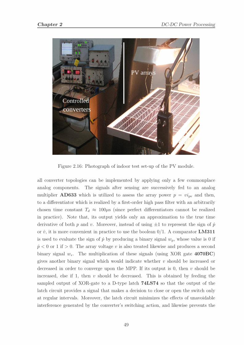
Chapter 2 DC-DC Power Processing
PV arrays
Controlled
converters
Figure 2.16: Photograph of indoor test set-up of the PV module.
all converter topologies can be implemented by applying only a few commonplace
analog components. The signals after sensing are successively fed to an analog
multiplier AD633 which is utilized to assess the array power p = vipv and then,
to a differentiator which is realized by a first-order high pass filter with an arbitrarily
chosen time constant Td ≈ 100µs (since perfect differentiators cannot be realized
in practice). Note that, its output yields only an approximation to the true time
derivative of both p and v. Moreover, instead of using ±1 to represent the sign of p
or v, it is more convenient in practice to use the boolean 0/1. A comparator LM311
is used to evaluate the sign of p by producing a binary signal wp, whose value is 0 if
p < 0 or 1 if > 0. The array voltage v is also treated likewise and produces a second
binary signal wv. The multiplication of these signals (using XOR gate 4070BC)
gives another binary signal which would indicate whether v should be increased or
decreased in order to converge upon the MPP. If its output is 0, then v should be
increased, else if 1, then v should be decreased. This is obtained by feeding the
sampled output of XOR-gate to a D-type latch 74LS74 so that the output of the
latch circuit provides a signal that makes a decision to close or open the switch only
at regular intervals. Moreover, the latch circuit minimizes the effects of unavoidable
interference generated by the converter’s switching action, and likewise prevents the
49
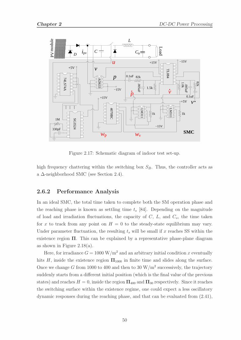
Chapter 2 DC-DC Power Processing
+5V
1k
CoP
Vm
odul
e
1k
82k
−15V
.005uF
AD
633
LM311
4070BC
74LS74A
SG
3524
LM311
TL084
L
ipv
0.1uF
330pF
+5V
1M
D.005uF
82k
0.1uF
C
−15V
+15V
+15V
pv
v
v
1.0k
1.5k
Load
−15V
w w
p
u
p vSMC
Figure 2.17: Schematic diagram of indoor test set-up.
high frequency chattering within the switching box SB. Thus, the controller acts as
a ∆-neighborhood SMC (see Section 2.4).
2.6.2 Performance Analysis
In an ideal SMC, the total time taken to complete both the SM operation phase and
the reaching phase is known as settling time ts [84]. Depending on the magnitude
of load and irradiation fluctuations, the capacity of C, L, and Co, the time taken
for x to track from any point on H = 0 to the steady-state equilibrium may vary.
Under parameter fluctuation, the resulting ts will be small if x reaches SS within the
existence region Π. This can be explained by a representative phase-plane diagram
as shown in Figure 2.18(a).
Here, for irradiance G = 1000 W/m2 and an arbitrary initial condition x eventually
hits H , inside the existence region Π1000 in finite time and slides along the surface.
Once we change G from 1000 to 400 and then to 30 W/m2 successively, the trajectory
suddenly starts from a different initial position (which is the final value of the previous
states) and reachesH = 0, inside the regionΠ400 andΠ30 respectively. Since it reaches
the switching surface within the existence regime, one could expect a less oscillatory
dynamic responses during the reaching phase, and that can be evaluated from (2.41),
50
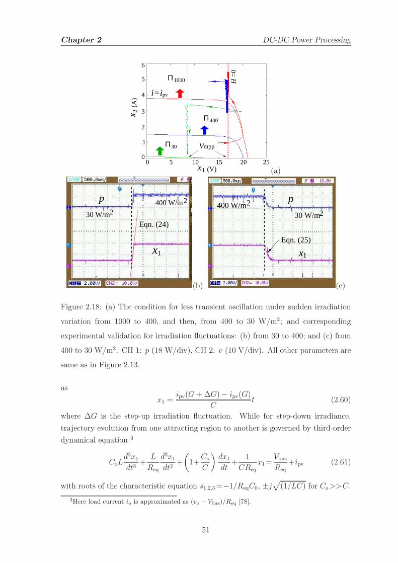
Chapter 2 DC-DC Power Processing
1 (V)
2(A
)
0 5 10 15 20 250
1
2
3
4
5
6
i=i pv
x
x
H=
0
400Π
Π1000
30Π Vmpp
(a)
30 W/m2400 W/m2
x
p
Eqn. (24)
1
(b)
2 p230 W/m
400 W/m
xEqn. (25)
1
(c)
Figure 2.18: (a) The condition for less transient oscillation under sudden irradiation
variation from 1000 to 400, and then, from 400 to 30 W/m2; and corresponding
experimental validation for irradiation fluctuations: (b) from 30 to 400; and (c) from
400 to 30 W/m2. CH 1: p (18 W/div), CH 2: v (10 V/div). All other parameters are
same as in Figure 2.13.
as
x1 =ipv(G+∆G)− ipv(G)
Ct (2.60)
where ∆G is the step-up irradiation fluctuation. While for step-down irradiance,
trajectory evolution from one attracting region to another is governed by third-order
dynamical equation 3
CoLd3x1
dt3+
L
Req
d2x1
dt2+
(
1+Co
C
)dx1
dt+
1
CReqx1=
Vbus
Req+ipv (2.61)
with roots of the characteristic equation s1,2,3=−1/ReqC0, ±j√
(1/LC) for Co>>C.
3Here load current io is approximated as (vo − Vbus)/Req [78].
51
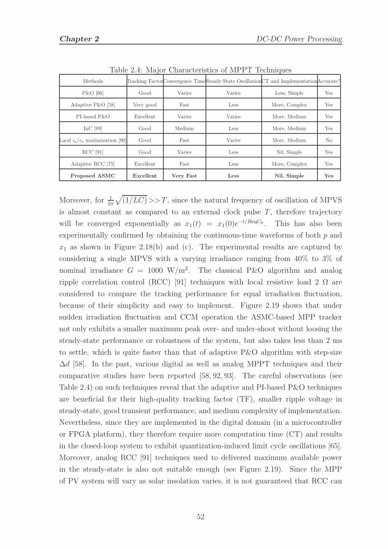
Chapter 2 DC-DC Power Processing
Table 2.4: Major Characteristics of MPPT Techniques
Methods Tracking FactorConvergence TimeSteady-State OscillationCT and ImplementationAccurate?
P&O [66] Good Varies Varies Less, Simple Yes
Adaptive P&O [58] Very good Fast Less More, Complex Yes
PI-based P&O Excellent Varies Varies More, Medium Yes
InC [89] Good Medium Less More, Medium Yes
Laod io/vo maximization [90] Good Fast Varies More, Medium No
RCC [91] Good Varies Less Nil, Simple Yes
Adaptive RCC [75] Excellent Fast Less More, Complex Yes
Proposed ASMC Excellent Very Fast Less Nil, Simple Yes
Moreover, for 12π
√
(1/LC)>>T , since the natural frequency of oscillation of MPVS
is almost constant as compared to an external clock pulse T , therefore trajectory
will be converged exponentially as x1(t) = x1(0)e−t/ReqC0 . This has also been
experimentally confirmed by obtaining the continuous-time waveforms of both p and
x1 as shown in Figure 2.18(b) and (c). The experimental results are captured by
considering a single MPVS with a varying irradiance ranging from 40% to 3% of
nominal irradiance G = 1000 W/m2. The classical P&O algorithm and analog
ripple correlation control (RCC) [91] techniques with local resistive load 2 Ω are
considered to compare the tracking performance for equal irradiation fluctuation,
because of their simplicity and easy to implement. Figure 2.19 shows that under
sudden irradiation fluctuation and CCM operation the ASMC-based MPP tracker
not only exhibits a smaller maximum peak over- and under-shoot without loosing the
steady-state performance or robustness of the system, but also takes less than 2 ms
to settle, which is quite faster than that of adaptive P&O algorithm with step-size
∆d [58]. In the past, various digital as well as analog MPPT techniques and their
comparative studies have been reported [58, 92, 93]. The careful observations (see
Table 2.4) on such techniques reveal that the adaptive and PI-based P&O techniques
are beneficial for their high-quality tracking factor (TF), smaller ripple voltage in
steady-state, good transient performance, and medium complexity of implementation.
Nevertheless, since they are implemented in the digital domain (in a microcontroller
or FPGA platform), they therefore require more computation time (CT) and results
in the closed-loop system to exhibit quantization-induced limit cycle oscillations [65].
Moreover, analog RCC [91] techniques used to delivered maximum available power
in the steady-state is also not suitable enough (see Figure 2.19). Since the MPP
of PV system will vary as solar insolation varies, it is not guaranteed that RCC can
52
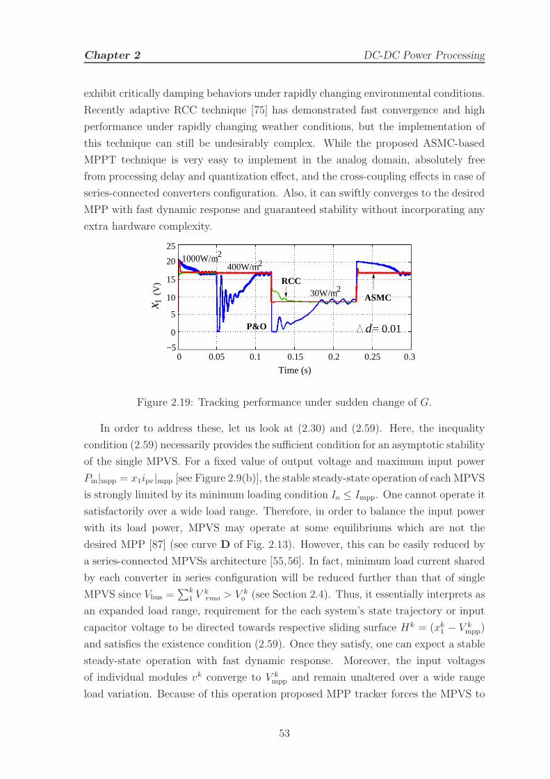
Chapter 2 DC-DC Power Processing
exhibit critically damping behaviors under rapidly changing environmental conditions.
Recently adaptive RCC technique [75] has demonstrated fast convergence and high
performance under rapidly changing weather conditions, but the implementation of
this technique can still be undesirably complex. While the proposed ASMC-based
MPPT technique is very easy to implement in the analog domain, absolutely free
from processing delay and quantization effect, and the cross-coupling effects in case of
series-connected converters configuration. Also, it can swiftly converges to the desired
MPP with fast dynamic response and guaranteed stability without incorporating any
extra hardware complexity.
(V)
1x
0
−5
25
0 0.05 0.1 0.15 0.2 0.25 0.3
20
15
10
5
Time (s)
= 0.01dP&O
RCC
ASMC
22
2
1000W/m
30W/m
400W/m
Figure 2.19: Tracking performance under sudden change of G.
In order to address these, let us look at (2.30) and (2.59). Here, the inequality
condition (2.59) necessarily provides the sufficient condition for an asymptotic stability
of the single MPVS. For a fixed value of output voltage and maximum input power
Pin|mpp = x1ipv|mpp [see Figure 2.9(b)], the stable steady-state operation of each MPVS
is strongly limited by its minimum loading condition Io ≤ Impp. One cannot operate it
satisfactorily over a wide load range. Therefore, in order to balance the input power
with its load power, MPVS may operate at some equilibriums which are not the
desired MPP [87] (see curve D of Fig. 2.13). However, this can be easily reduced by
a series-connected MPVSs architecture [55,56]. In fact, minimum load current shared
by each converter in series configuration will be reduced further than that of single
MPVS since Vbus =∑k
1 Vkrmo > V k
o (see Section 2.4). Thus, it essentially interprets as
an expanded load range, requirement for the each system’s state trajectory or input
capacitor voltage to be directed towards respective sliding surface Hk = (xk1 − V k
mpp)
and satisfies the existence condition (2.59). Once they satisfy, one can expect a stable
steady-state operation with fast dynamic response. Moreover, the input voltages
of individual modules vk converge to V kmpp and remain unaltered over a wide range
load variation. Because of this operation proposed MPP tracker forces the MPVS to
53
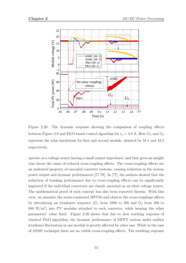
Chapter 2 DC-DC Power Processing
−5
00.1.05 .06 .07 .08 .09 .11 .12 .13 .14
25
20
15
10
5
0
80
60
Mod
ule
volta
ge (
V)
Tot
al P
V p
ower
(W
)
40
20
.15
Time (s)
1G2G
ASMC
P&O
No cross−coupling effects
ASMC (M−2)P&O (M−2)P&O (M−1)
ASMC (M−1)
Figure 2.20: The dynamic response showing the comparison of coupling effects
between Figure 2.9 and P&O based control algorithm for io = 4.8 A. Here G1 and G2
represent the solar insolations for first and second module, denoted by M-1 and M-2
respectively.
operate as a voltage source having a small output impedance, and thus gives an insight
clue about the cause of reduced cross-coupling effects. The cross-coupling effects are
an undesired property of cascaded converter systems, causing reduction in the system
power output and dynamic performances [77,79]. In [77], the authors showed that the
reduction of tracking performance due to cross-coupling effects can be significantly
improved if the individual converters are closely operated as an ideal voltage source.
The mathematical proof of such concept has also been reported therein. With this
view, we simulate the series-connected MPVSs and observe the cross-couplings effects
by introducing an irradiance sequence (G1 from 1000 to 500 and G2 from 400 to
800 W/m2) into PV modules attached to each converter, while keeping the other
parameters’ value fixed. Figure 2.20 shows that due to slow tracking response of
classical P&O algorithm, the dynamic performance of MPPT system under sudden
irradiance fluctuation in one module is greatly affected by other one. While in the case
of ASMC technique there are no visible cross-coupling effects. The resulting response
54

Chapter 2 DC-DC Power Processing
in the input voltages of the converters is not affected by the disturbance caused by
any changes in other PV module’s irradiance. Thus, it improves the energy yield of
the system.
(W)
,
0
2
22
25
20
15
10
5
3020 40 50 60
Time (ms)
(a)
inPoP
oPPin
80W/m
350W/m
150W/m
(b)
80 W/m2
CLK
350 W/m
150 W/m2
2
inP
Figure 2.21: (a) Representative diagram showing the transient performances of Pin
and P do (without any cross-coupling effects) for io = 4.8 A and Req = 0.02 Ω; and (b)
its experimental confirmation. CH 1 is the clock pulse and CH 2 is the input power
Pin ≈ 9 W/div.
Table 2.5: η (%) of series configuration for different G1 (W/m2) when io = 4.8 A and
Req= 0.02 Ω
G1 1000 850 700 550 400 250 50
η 97.52 97.28 96.68 96.66 96.60 96.11 92.76
Moreover, since the efficiency of the overall system is determined by stable
steady-state behavior and transient response of MPPT efficiency [70], therefore, the
highest possible efficiency can only be achieved if the existence condition (2.59)
is satisfied. With this view, system dynamics are analyzed and also validated
experimentally over a wide range of rapidly fluctuating irradiances. The test has been
performed in indoor by considering a string of two series-connected MPVSs, and each
of them is artificially illuminated by different levels irradiances G1 = 350 and G2 =
40 W/m2 (measured by Pyrometer). We then successively change the insolation level
G1 from 350-to-150-to-80, and back to 350 W/m2 without varying G2. Figure 2.21(a)
55

Chapter 2 DC-DC Power Processing
and (b) reveal that proposed ASMC-based series architecture not only tracks the true
MPP of each module efficiently, but is also able to locate and extract the maximum
available power from the PV array under any mismatching conditions (see Table 2.5).
One cannot achieve it, simply by iteratively changing the duty ratio of individual
dc-dc converter under such rapidly changing inhomogeneous solar irradiances.
2.7 Conclusion
In this chapter, an analog circuitry based fast and robust MPP tracker is proposed
for buck, boost, and buck-boost-type modular PV systems. Based on the condition
of SM in HDSs, the exact mathematical models for all such converter systems were
derived. Discussion on the modeling and analysis were done to design and extract the
best optimized performances (in terms of steady-state and transient responses with
improved overall systems’ efficiency) using the concepts of equivalent control law and
fast-scale stability analysis. These are experimentally verified by taking an example of
buck-type MIC and compared with P&O based algorithm. The results demonstrate
that under sudden irradiation fluctuations, the tracking performances of analog MPP
tracker employing SMC is not only faster than the reference one, but also exhibits
less steady-state oscillations with reduced cross-coupling effects. One drawback of this
method is that if the converter’s switching frequency varies, it is required to redesign
the high pass filter circuit which is used to obtain the time derivatives of module
current and voltage. Moreover, hardware realization of boost-type tracker and also
its use in cascaded converters architecture is a subject of the future investigation.
56
Chapter 3
DC-AC Power Processing
In dual-stage GPV systems, after boosting the voltage from low PV module voltage to
a high dc bus voltage, the dc-ac inverter stage is employed to convert dc power into ac
power and feed the power into the utility grid. In low or medium-scale applications,
the galvanic isolation is not required, if the ground leakage current is under a certain
limit. There are a lot of inverter topologies are reported based on output power, the
total current harmonics and the cost. The different topologies of the inverter with their
proper switching technique will be discussed in this chapter. The stand-alone mode
of operation with a fixed dc supply will be considered here. Since, maintaining good
voltage regulation and achieving fast dynamic response under sudden load fluctuation
are extremely important for a dc-ac inverter system; two current control schemes will
therefore be discussed to address the above power quality issues.
3.1 1-φ Inverter Topologies
Single-phase inverters are mostly used in the domestic sector. The majority of such
inverter systems can have up to 5kW and are roof mounted. Based on the input
supply, the 1-φ dc-ac inverter topologies can be divided into two groups: voltage
source inverter (VSI), and current source inverter (CSI), which are shown separately
in Figure 3.1 [94], [95]. VSI are commonly used for low or medium power level of
dc-ac power conversion, whereas CSI is used for the high power applications. A large
inductor is connecting in series with the dc bus voltage which makes CSI bulky and
expensive. As a series diode is connected with the main switches in CSI topologies to
block the reverse voltage which may also increase the conduction losses. Due to these
drawbacks, CSI has limited applications. On the other hand, VSI is the dominant
57

Chapter 3 DC-AC Power Processing
topology in PV system due to the following advantages:
S
S4S2
S3 1
C R
(a)
L
CdcPV
S
S4S2
S3 1
dL
dc−
link
C R
L
(b)
Figure 3.1: Schematic diagram of inverter topologies: (a) VSI; (b) CSI.
• VSI uses self-commutating switching circuit.
• As a capacitor is connected in between PV output and inverter, so it handles
the output current regulation and dc bus voltage regulation.
• The output voltage waveform is mostly remaining unchanged by the load.
• Broad power level applications.
• Efficiency can be improved by using proper switching techniques.
Based on the commutation process, most of the inverter topologies are either line
frequency-commutated inverters or self-commutated inverters [94], [95]. Generally,
line frequency-commutated inverter uses a sinusoidal signal to generate the ac output.
These are commonly used due to the efficient power conversion and low cost. But the
drawbacks with this configuration are the poor power quality of the output voltage
and have a power factor between 0.6 and 0.7 [95]. On the other hand, self-commutated
inverters are commonly used because it can operate at high switching frequency, which
produces a low THD output voltage. Moreover they are robust and cheap.
Single-phase half bridge and full bridge inverter topologies are commonly used in
PV system as the dc-ac power processing stage. In half bridge inverter topology, two
equal capacitors are connected back-to-back across the dc input, so that a voltage of
E (supply voltage) appear across each capacitor. Both the switches are operated in
the complementary mode so that the output voltage varies from -E to +E. The LC
low pass filter is used at the output of the inverter to minimize the high switching
harmonics. On the other hand, a full bridge inverter is also known as H-bridge inverter
58
Chapter 3 DC-AC Power Processing
consists of two half bridge inverters. The output voltage of this inverter is twice that
of the half-bridge inverter, which implies that for the same power, the current rating
in the former case is half of the later. These topologies are used in high power
applications. So, a 1-Φ full bridge VSI is considered throughout the thesis for the
dc-ac power conversion. This topology can also be used in UPS applications.
3.2 Modulation Techniques for VSI
Pulse width modulation (PWM) techniques of VSI have been the subject of intensive
research over the last several years as the primary strategy to control the ac output
voltage or current of a dc-ac converter [96]. The concept of PWM is to control the duty
cycle of each switch at a high switching frequency to generate a train of controlled
pulses that have the required low-frequency fundamental component. The second
objective of these PWM schemes is to arrange the switching pulses in such a way that
it can minimize the unwanted harmonic components and the switching losses. The
classical and most widely used modulation technique for a VSI is naturally sampled
sine pulse width modulation(SPWM) [96]. Here, a low-frequency voltage control
signal (sine wave) is compared with a high-frequency carrier, i.e., triangular signal
and the comparison result, which is a logic output, is used to determine the on or
off-state of the power switches. The frequency of the triangular signal determines the
inverter switching frequency. Out of four switches of the inverter, S1, S2, and S3, S4
are operated in a complementary manner, and to avoid the short circuit between
these switches, a dead time has to be introduced. Naturally sampled SPWM does
not control the position of the pulses it generates in each cycle and the minimum
pulse width is not controlled. But uniformly sampled SPWM technique also requires
a triangle carrier signal at switching frequency but it only uses the comparison result
to determine the on or off duration of the switches but not the pulse position. The
pulse position is uniformly controlled, e.g., put at the center of every switching cycle.
Another common form of PWM technique for VSI is space-vector modulation [97].
The primary advantage of this modulation technique over classical sinusoidal PWM
is the explicit identification of the pulse placement within each carrier period as an
extra degree of freedom, that has been shown to improve the harmonic performance of
the inverter. However, implementation of this scheme is quite complex and commonly
used in the poly-phase system.
Consequently, other methods like multi-carrier PWM and selective harmonic
elimination PWM are used for harmonic elimination in VSI [96]. These techniques
59
Chapter 3 DC-AC Power Processing
are widely used because it can be easily implemented for low voltage applications [98].
Normally harmonic elimination methods can be classified as level-shifted PWM and
phase-shifted PWM methods [99]. The level Shifted-PWM is characterized into
phase disposition, phase opposition disposition and alternative phase opposition
disposition [100]. Compared to the all above techniques, alternative phase opposition
disposition method is the most major process to express harmonics are centered as
sidebands around the carrier frequency [101]. Merits of this approach in multi-carrier
PWM have no harmonics occur at the carrier frequency and higher band width [102].
Among all the above methods, selective harmonic elimination PWM is the only
method for selecting proper switching angles to eliminate low-order harmonics and
minimize the THD of the output voltage. The main objective of this method is
to determine the switching angles to specific lower order harmonics suppressed in
the output voltage of the inverter to achieve desired fundamental component with
possible minimum THD [103]. This method operates a set of non-linear transcendental
equations as the fitness or objective function that includes many local optimal
solutions [104]. But all the above modulation techniques are applicable to voltage
mode control of the inverters.
On the other hand, the hysteresis-band current controlled modulation technique
is the most popular because of its simplicity in implementation, inherently limiting
the over-current and very fast response. Hysteresis-band PWM techniques generate
the switching pulse for the inverter switches based on a nonlinear feedback loop with
two-level hysteresis comparators. The current error is allowed to pass through a
band so that the switching states are defined by the upper and lower envelope of the
band. The switching frequency of the inverter is decided by the width of the band.
The only disadvantage of this PWM technique; the operating switching frequency
depends largely on the load parameters and varies with the ac voltage. However,
several methods are proposed for the constant switching operation, which will be
discussed later. Hence, this modulation technique is used throughout this thesis to
generate the controlled switching pulse for the inverter.
Based on the level of the output voltage of the inverter, the PWM techniques are
further classified into two categories, which are discussed below.
3.2.1 1-φ Bridge Topology with Bipolar PWM
The bipolar switching scheme by using the hysteresis band is shown in Figure 3.2(a).
In bipolar switching scheme, the error current is passed through a single hysteresis
band to control the turn on and turn off period of the switching pairs; S1, S2, and
60
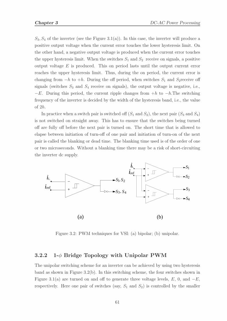
Chapter 3 DC-AC Power Processing
S3, S4 of the inverter (see the Figure 3.1(a)). In this case, the inverter will produce a
positive output voltage when the current error touches the lower hysteresis limit. On
the other hand, a negative output voltage is produced when the current error touches
the upper hysteresis limit. When the switches S1 and S2 receive on signals, a positive
output voltage E is produced. This on period lasts until the output current error
reaches the upper hysteresis limit. Thus, during the on period, the current error is
changing from −h to +h. During the off period, when switches S1 and S2receive off
signals (switches S3 and S4 receive on signals), the output voltage is negative, i.e.,
−E. During this period, the current ripple changes from +h to −h.The switching
frequency of the inverter is decided by the width of the hysteresis band, i.e., the value
of 2h.
In practice when a switch pair is switched off (S1 and S2), the next pair (S3 and S4)
is not switched on straight away. This has to ensure that the switches being turned
off are fully off before the next pair is turned on. The short time that is allowed to
elapse between initiation of turn-off of one pair and initiation of turn-on of the next
pair is called the blanking or dead time. The blanking time used is of the order of one
or two microseconds. Without a blanking time there may be a risk of short-circuiting
the inverter dc supply.
S1,S2
S3, S4
i
iref
L
(a)
+
−
L S
S2
S
1
S4
3
iref
i
(b)
+
−
+
−
Figure 3.2: PWM techniques for VSI: (a) bipolar; (b) unipolar.
3.2.2 1-φ Bridge Topology with Unipolar PWM
The unipolar switching scheme for an inverter can be achieved by using two hysteresis
band as shown in Figure 3.2(b). In this switching scheme, the four switches shown in
Figure 3.1(a) are turned on and off to generate three voltage levels, E, 0, and −E,
respectively. Here one pair of switches (say, S1 and S2) is controlled by the smaller
61
Chapter 3 DC-AC Power Processing
hysteresis band and another pair of switches (S3 and S4) is controlled by the larger
hysteresis band. The current error is mainly decided by the smaller hysteresis band.
When the smaller hysteresis band has lost its ability to control the current error, then
only the larger hysteresis band is active. The smaller hysteresis band cannot control
the current error when the output voltage polarity is reversed. In this condition, the
polarity of the output voltage can be reversed by the larger hysteresis band. Thus, the
pair of switching devices that is controlled by the larger hysteresis band is switched
at the fundamental output frequency. During the positive half-cycle of the output
voltage, switch S2 (switch S3) receives an on signal (off signal). On the other hand,
during the negative half-cycle of the output voltage, switch S2 (switch S3) receives an
off signal (on signal). The output current error is controlled by switches S1 and S4.
The output voltage has a unipolar characteristic similar to the symmetrical unipolar
carrier-based PWM.
As implementation of unipolar PWM scheme is quite complex, so bipolar PWM
technique is commonly used for switching the inverter.
3.2.3 LC Filter Design for 1-φ VSI
The first design consideration is the selection of components which can be determined
by setting criteria on ripple current and filtering criteria. First of all, the inductor L
can be selected by the ripple current in the inductor. A larger inductance value allows
a smaller inductor switching ripple; however, a large inductance value will increase
the cost, volume, and weight of the inductor. Thus, the choice of the inductor value is
a trade-off between ripple current specification and cost. Second, the filter capacitor
C is calculated by the cut-off frequency of the LC second-order filter for the output
voltage v0 under standalone mode. The cut-off frequency of the LC filter is suggested
to be between 10 times lesser than switching frequency and 10 times higher than the
fundamental frequency.
3.3 Classical Control Methods for 1-φ VSI
The PWM VSI is extensively used in ac power conditioning systems. A 1-φ VSI
supplies the non-linear and critical step changing loads. The above loads deform the
desired sinusoidal output voltage of inverter [105]. For all types of loads the THD of
the inverter output voltage should be as per the IEEE standard 1547, i.e., less than
5%. Moreover, current-controlled inverter should be met the following substantial
62
Chapter 3 DC-AC Power Processing
performances; fast transient response, low current ripple in the steady-state, optimal
switching pattern and stability for the load variation. In recent past, several control
strategies have been suggested for the inverter operations depending on how the
current or voltage error signal is processed. A review of different current control
techniques used for VSI are discussed here.
I. Conventional PI controls
The control technique based on proportional-integral (PI) controller in the
stationary reference frame where the PI regulators have to track sinusoidally
varying inputs [106]. Since PI controller only guarantees zero steady state
error under dc reference input, this control technique cannot be performed
well. Another control technique based on proportional control plus model-based
compensation was proposed [107]. It does not require the information that
the reference input is a 50 Hz sine wave so that the control design has to
be able to handle arbitrary input, which is unlikely to achieve a good control
performance for inverter applications. An inverter control technique based on
PI regulation only was developed [108]. Even though the system is required to
handle harmonic current, no theoretical measure has been taken to address the
issue. A dual loop proportional control scheme have designed for 1-φ half-bridge
inverters in island mode [109]. The authors have analyzed through the small
signal frequency domain analysis to stabilize the closed-loop system. However,
the simple proportional controller can not provide satisfactory performances in
either steady state or transient.
II. Proportional-resonant control
A proportional-resonant (PR) controller is commonly used in a stationary
reference frame control like abc or αβ frame. These controllers have achieved
a high gain around resonant frequency and thus is capable of eliminating a
steady state error, when control variables are sinusoidal [110], [111], [112]. In
this controller, a low order harmonics compensator can be easily implemented
to improve the performance of the current controller without influencing its
behavior [110]. In order to maintain good performance of the controller, the
resonant frequency must be identical to the frequency of the output voltage.
The frequency can be adaptively adjusted according to output voltage frequency
variation as reported in [112].
63
Chapter 3 DC-AC Power Processing
III. Deadbeat control
Deadbeat (DB) predictive controllers are widely used for sinusoidal
current regulation of different applications due to its good dynamic
performance [113], [114], [115]. Theoretically, this controller has a very high
bandwidth and hence, tracking of sinusoidal signals is very good. The principle
of the DB controller is to calculate the derivative of the controlled variable in
order to predict the effect of the control action. Deadbeat predictive control
is widely used for current error compensation and offers high performance for
current-controlled VSIs. However, it is quite complicated and sensitive to system
parameters [113], [114].
IV. Multiloop control
A multi-loop feedback controller is suitable to meet the above requirements.
Generally, this controller is used to control the output voltage or current of a
VSI when it equipped with a high order LC or LCL passive filter. It involves the
use of an outer and an inner current loop. The outer loop ensuring the steady
state performance and the inner loop providing the transient performance and
improving the stability [116]. The stand-alone or grid-connected PV systems
have to be controlled in such a way that the output voltage or current should
be in phase with an external sinusoidal reference proportional to the utility
grid. Hence, this external sinusoidal reference is included in the control loop.
In these cases, the control loop design is based on the minimization of the error
defined as the difference between the reference signal and the output signal.
This control method is known as a “tracking” control scheme, in the sense that
the output signal is constrained to track the reference by means of the control
action. In stand-alone systems, a multi-loop voltage controller with a capacitor
current feedback as inner loop can eliminate the output LC filter resonant peak
to increase stability in load disturbance and enhance dynamic performance [117].
V. Intelligent control
Besides above conventional control, intelligent control can also be applied
to inverter control. A fuzzy logic controller has developed for voltage loop
regulation which yields a satisfactory performance [118]. However, the control
rules are based on empirical knowledge which cannot be obtained directly.
VI. Sliding mode control
A non-linear control scheme, namely, sliding mode control (SMC) strategy
64
Chapter 3 DC-AC Power Processing
has been proposed in inverter control since these are well known for their
robustness, guaranteed stability and good dynamic response under the wide
range of operating conditions. The SMC utilizes a switching control law to
drive the state trajectory from any initial positions to a specified surface in the
state space called sliding or switching surface and maintain it on this surface
for all subsequent time [119]. However, SMC operates at variable switching
frequency at which an undesirable chattering phenomenon may occur. In order
to compensate the above drawback partially, the SMC are realized by means of a
hysteresis comparator [120], which also provides a variable switching frequency.
Several authors have proposed constant frequency SMC by means of a variable
width hysteresis controller [121], which can however lead to a complex analog
implementation, thereby involve more cost. Moreover, the width of hysteresis
band depends on the converter parameters. Alternatively, fixed frequency SMC
can also be achieved by comparing an external ramp signal to the switching
surface [122]. Hence in these controllers, the switching instant does not depend
on the switching surface behavior.
Over the past decades, many efforts have been devoted to this research area
and references therein [115,120]. A discrete-time sliding mode control technique
has developed for 1-φ inverters in both voltage and current loops [123]. In
this technique, the control variable in each sampling period is calculated based
on the plant model and feedback quantities. The control is continuous and
the chattering problem does not exist. The presented results show good
performances under both linear and nonlinear loads. However implementation
of this controller is quite complex, and involve more cost. Another SMC control
technique using deadbeat current control and proportional voltage control was
proposed [115]. The deadbeat control concept is suitable when the plant model
parameters are known. The presented result is reasonably good. However, its
dependence on knowledge of plant parameters limits its application as an outer
loop controller in multi-loop feedback systems.
Based on the above discussion, SMC is suitable for improving both steady-state
and dynamic performance of an inverter system. More details, including SMC design,
is discussed in this chapter. Two SMC controllers are proposed to address these issues.
First, a fixed frequency hysteretic current (FFHC) controller is proposed on the basis
of SMC. The Proposed controller is compared with the carrier based PWM voltage
controller under the same load fluctuation to evaluate its performance. Then, another
sensorless SMC scheme is also designed for the same inverter by taking an ellipsoidal
65
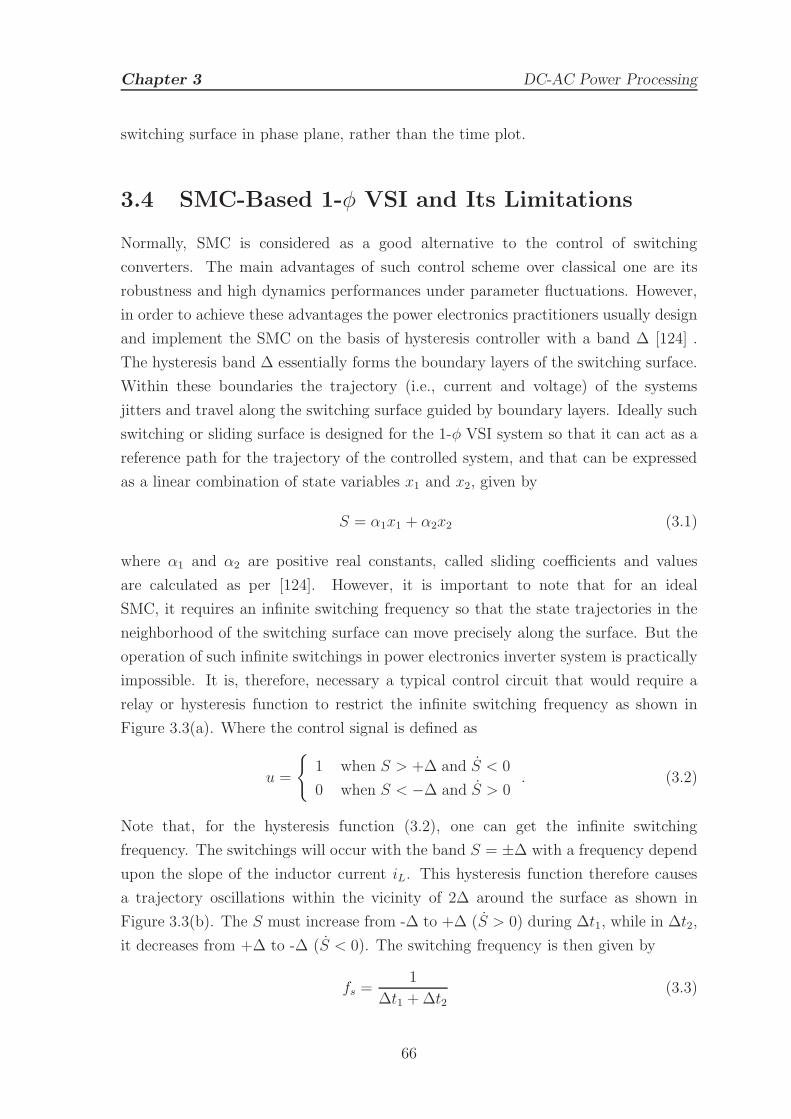
Chapter 3 DC-AC Power Processing
switching surface in phase plane, rather than the time plot.
3.4 SMC-Based 1-φ VSI and Its Limitations
Normally, SMC is considered as a good alternative to the control of switching
converters. The main advantages of such control scheme over classical one are its
robustness and high dynamics performances under parameter fluctuations. However,
in order to achieve these advantages the power electronics practitioners usually design
and implement the SMC on the basis of hysteresis controller with a band ∆ [124] .
The hysteresis band ∆ essentially forms the boundary layers of the switching surface.
Within these boundaries the trajectory (i.e., current and voltage) of the systems
jitters and travel along the switching surface guided by boundary layers. Ideally such
switching or sliding surface is designed for the 1-φ VSI system so that it can act as a
reference path for the trajectory of the controlled system, and that can be expressed
as a linear combination of state variables x1 and x2, given by
S = α1x1 + α2x2 (3.1)
where α1 and α2 are positive real constants, called sliding coefficients and values
are calculated as per [124]. However, it is important to note that for an ideal
SMC, it requires an infinite switching frequency so that the state trajectories in the
neighborhood of the switching surface can move precisely along the surface. But the
operation of such infinite switchings in power electronics inverter system is practically
impossible. It is, therefore, necessary a typical control circuit that would require a
relay or hysteresis function to restrict the infinite switching frequency as shown in
Figure 3.3(a). Where the control signal is defined as
u =
1 when S > +∆ and S < 0
0 when S < −∆ and S > 0. (3.2)
Note that, for the hysteresis function (3.2), one can get the infinite switching
frequency. The switchings will occur with the band S = ±∆ with a frequency depend
upon the slope of the inductor current iL. This hysteresis function therefore causes
a trajectory oscillations within the vicinity of 2∆ around the surface as shown in
Figure 3.3(b). The S must increase from -∆ to +∆ (S > 0) during ∆t1, while in ∆t2,
it decreases from +∆ to -∆ (S < 0). The switching frequency is then given by
fs =1
∆t1 +∆t2(3.3)
66
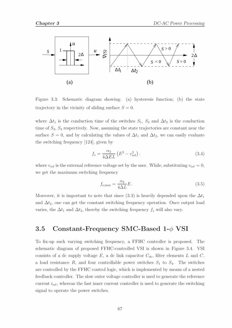
Chapter 3 DC-AC Power Processing
2u
(a)
S
u
∆1
< 0
> 0
(S)
∆
(b)
t t
∆2
∆ ∆1 2
S
S = 0S
Figure 3.3: Schematic diagram showing: (a) hysteresis function; (b) the state
trajectory in the vicinity of sliding surface S = 0.
where ∆t1 is the conduction time of the switches S1, S2 and ∆t2 is the conduction
time of S3, S4 respectively. Now, assuming the state trajectories are constant near the
surface S = 0, and by calculating the values of ∆t1 and ∆t2, we can easily evaluate
the switching frequency [124], given by
fs =α2
4∆EL
(E2 − v2ref
). (3.4)
where vref is the external reference voltage set by the user. While, substituting vref = 0,
we get the maximum switching frequency
fs,max =α2
4∆LE. (3.5)
Moreover, it is important to note that since (3.3) is heavily depended upon the ∆t1
and ∆t2, one can get the constant switching frequency operation. Once output load
varies, the ∆t1 and ∆t2, thereby the switching frequency fs will also vary.
3.5 Constant-Frequency SMC-Based 1-φ VSI
To fix-up such varying switching frequency, a FFHC controller is proposed. The
schematic diagram of proposed FFHC-controlled VSI is shown in Figure 3.4. VSI
consists of a dc supply voltage E, a dc link capacitor Cdc, filter elements L and C,
a load resistance R, and four controllable power switches S1 to S4. The switches
are controlled by the FFHC control logic, which is implemented by means of a nested
feedback controller. The slow outer voltage controller is used to generate the reference
current iref , whereas the fast inner current controller is used to generate the switching
signal to operate the power switches.
67
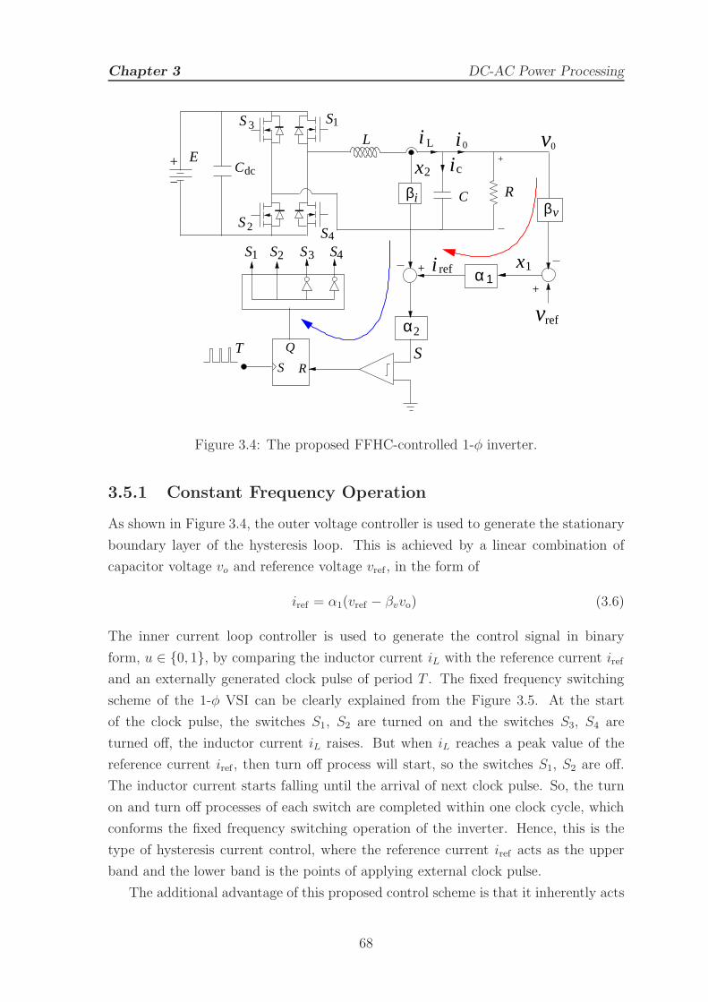
Chapter 3 DC-AC Power Processing
T
vrefα2
S
+
dcC
ref α
β
iL
S4
0
Q
1i
i L i 0vE
S2
S3
21S 3 S4S S
c
1
vβ
+
RC
1x
S
x2
RS
i
+
−
+
Figure 3.4: The proposed FFHC-controlled 1-φ inverter.
3.5.1 Constant Frequency Operation
As shown in Figure 3.4, the outer voltage controller is used to generate the stationary
boundary layer of the hysteresis loop. This is achieved by a linear combination of
capacitor voltage vo and reference voltage vref , in the form of
iref = α1(vref − βvvo) (3.6)
The inner current loop controller is used to generate the control signal in binary
form, u ∈ 0, 1, by comparing the inductor current iL with the reference current iref
and an externally generated clock pulse of period T . The fixed frequency switching
scheme of the 1-φ VSI can be clearly explained from the Figure 3.5. At the start
of the clock pulse, the switches S1, S2 are turned on and the switches S3, S4 are
turned off, the inductor current iL raises. But when iL reaches a peak value of the
reference current iref , then turn off process will start, so the switches S1, S2 are off.
The inductor current starts falling until the arrival of next clock pulse. So, the turn
on and turn off processes of each switch are completed within one clock cycle, which
conforms the fixed frequency switching operation of the inverter. Hence, this is the
type of hysteresis current control, where the reference current iref acts as the upper
band and the lower band is the points of applying external clock pulse.
The additional advantage of this proposed control scheme is that it inherently acts
68
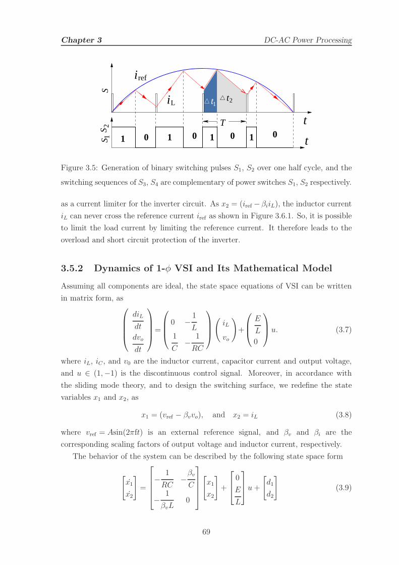
Chapter 3 DC-AC Power Processing
0 0 01 1 1
ref
t
i
Li
t1 0
SS 2
S 1
T
12tt
Figure 3.5: Generation of binary switching pulses S1, S2 over one half cycle, and the
switching sequences of S3, S4 are complementary of power switches S1, S2 respectively.
as a current limiter for the inverter circuit. As x2 = (iref −βiiL), the inductor current
iL can never cross the reference current iref as shown in Figure 3.6.1. So, it is possible
to limit the load current by limiting the reference current. It therefore leads to the
overload and short circuit protection of the inverter.
3.5.2 Dynamics of 1-φ VSI and Its Mathematical Model
Assuming all components are ideal, the state space equations of VSI can be written
in matrix form, as
diL
dt
dvo
dt
=
0 −1
L1
C−
1
RC
(
iL
vo
)
+
E
L
0
u. (3.7)
where iL, iC , and v0 are the inductor current, capacitor current and output voltage,
and u ∈ (1,−1) is the discontinuous control signal. Moreover, in accordance with
the sliding mode theory, and to design the switching surface, we redefine the state
variables x1 and x2, as
x1 = (vref − βvvo), and x2 = iL (3.8)
where vref = Asin(2πft) is an external reference signal, and βv and βi are the
corresponding scaling factors of output voltage and inductor current, respectively.
The behavior of the system can be described by the following state space form
[
x1
x2
]
=
−1
RC−βv
C
−1
βvL0
[
x1
x2
]
+
0
E
L
u+
[
d1
d2
]
(3.9)
69

Chapter 3 DC-AC Power Processing
where d1 and d2 are the disturbance terms defined as
d1 =dvref
dt+
1
βv
vref
Rand d2 =
vref
LIn compact form
x = Ax+Bu+D (3.10)
The main objective of sliding mode control is to operate the switches as a function
of the state variables to direct the system trajectory to converge at the desired
equilibrium point by designing a suitable sliding surface in the state space. In this
work, multi-loop with position controller is used for investigation. For the system
slides on the sliding surface, the switching control law is given by
u =
1 for S > 0
−1 for S < 0(3.11)
where the sliding function is given by
S(x, t) = αi(αv(vref − βvv)− βiiL) (3.12)
S(x, t) = αiαvx1 − αiβix2 = JTx (3.13)
with sliding coefficients JT = [αiαv −αiβi]. A sliding surface is obtained by satisfying
the condition S = 0.
The existence condition for sliding mode operation can be found by using
Lyapunov’s direct method to solve SS < 0, which gives the existence region of sliding
mode. By substituting (3.10), (3.11) and (3.13) to SS < 0, the existence condition is
given by
SS→0+ = JTAx+ JTB + JTD < 0
SS→0− = JTAx− JTB + JTD > 0(3.14)
The above inequalities give the existence condition of the SMC as well as the design
range for the sliding coefficients, which should ensure the system to remain in sliding
mode operation when the system trajectory is close to the sliding surface.
In SMC operation, the dynamics of the system can be characterized using the
invariance conditions S = 0 and S = 0. With the condition S = 0, the system can be
represented as
S(x, t) = αiαvx1 − αiβix2 = 0 (3.15)
70
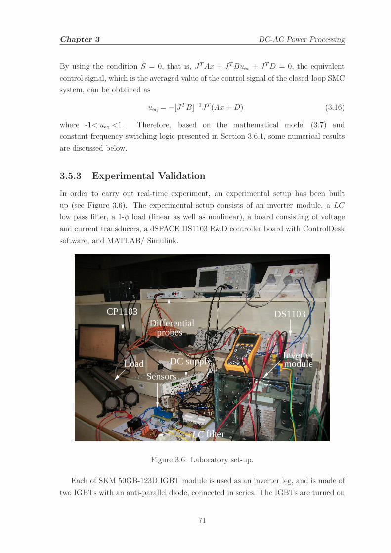
Chapter 3 DC-AC Power Processing
By using the condition S = 0, that is, JTAx + JTBueq + JTD = 0, the equivalent
control signal, which is the averaged value of the control signal of the closed-loop SMC
system, can be obtained as
ueq = −[JTB]−1JT (Ax+D) (3.16)
where -1< ueq <1. Therefore, based on the mathematical model (3.7) and
constant-frequency switching logic presented in Section 3.6.1, some numerical results
are discussed below.
3.5.3 Experimental Validation
In order to carry out real-time experiment, an experimental setup has been built
up (see Figure 3.6). The experimental setup consists of an inverter module, a LC
low pass filter, a 1-φ load (linear as well as nonlinear), a board consisting of voltage
and current transducers, a dSPACE DS1103 R&D controller board with ControlDesk
software, and MATLAB/ Simulink.
LoadSensors
Inverter
LC
DifferentialDS1103CP1103
probes
moduleDC supply
filter
Figure 3.6: Laboratory set-up.
Each of SKM 50GB-123D IGBT module is used as an inverter leg, and is made of
two IGBTs with an anti-parallel diode, connected in series. The IGBTs are turned on
71
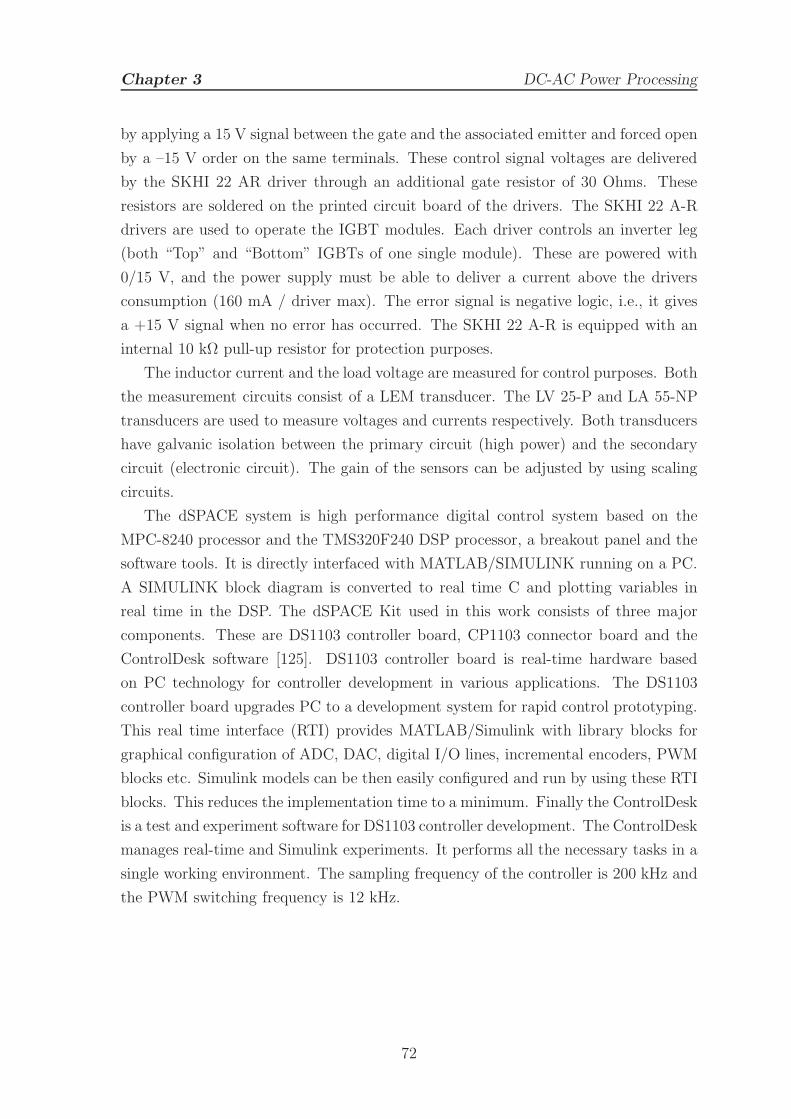
Chapter 3 DC-AC Power Processing
by applying a 15 V signal between the gate and the associated emitter and forced open
by a –15 V order on the same terminals. These control signal voltages are delivered
by the SKHI 22 AR driver through an additional gate resistor of 30 Ohms. These
resistors are soldered on the printed circuit board of the drivers. The SKHI 22 A-R
drivers are used to operate the IGBT modules. Each driver controls an inverter leg
(both “Top” and “Bottom” IGBTs of one single module). These are powered with
0/15 V, and the power supply must be able to deliver a current above the drivers
consumption (160 mA / driver max). The error signal is negative logic, i.e., it gives
a +15 V signal when no error has occurred. The SKHI 22 A-R is equipped with an
internal 10 kΩ pull-up resistor for protection purposes.
The inductor current and the load voltage are measured for control purposes. Both
the measurement circuits consist of a LEM transducer. The LV 25-P and LA 55-NP
transducers are used to measure voltages and currents respectively. Both transducers
have galvanic isolation between the primary circuit (high power) and the secondary
circuit (electronic circuit). The gain of the sensors can be adjusted by using scaling
circuits.
The dSPACE system is high performance digital control system based on the
MPC-8240 processor and the TMS320F240 DSP processor, a breakout panel and the
software tools. It is directly interfaced with MATLAB/SIMULINK running on a PC.
A SIMULINK block diagram is converted to real time C and plotting variables in
real time in the DSP. The dSPACE Kit used in this work consists of three major
components. These are DS1103 controller board, CP1103 connector board and the
ControlDesk software [125]. DS1103 controller board is real-time hardware based
on PC technology for controller development in various applications. The DS1103
controller board upgrades PC to a development system for rapid control prototyping.
This real time interface (RTI) provides MATLAB/Simulink with library blocks for
graphical configuration of ADC, DAC, digital I/O lines, incremental encoders, PWM
blocks etc. Simulink models can be then easily configured and run by using these RTI
blocks. This reduces the implementation time to a minimum. Finally the ControlDesk
is a test and experiment software for DS1103 controller development. The ControlDesk
manages real-time and Simulink experiments. It performs all the necessary tasks in a
single working environment. The sampling frequency of the controller is 200 kHz and
the PWM switching frequency is 12 kHz.
72
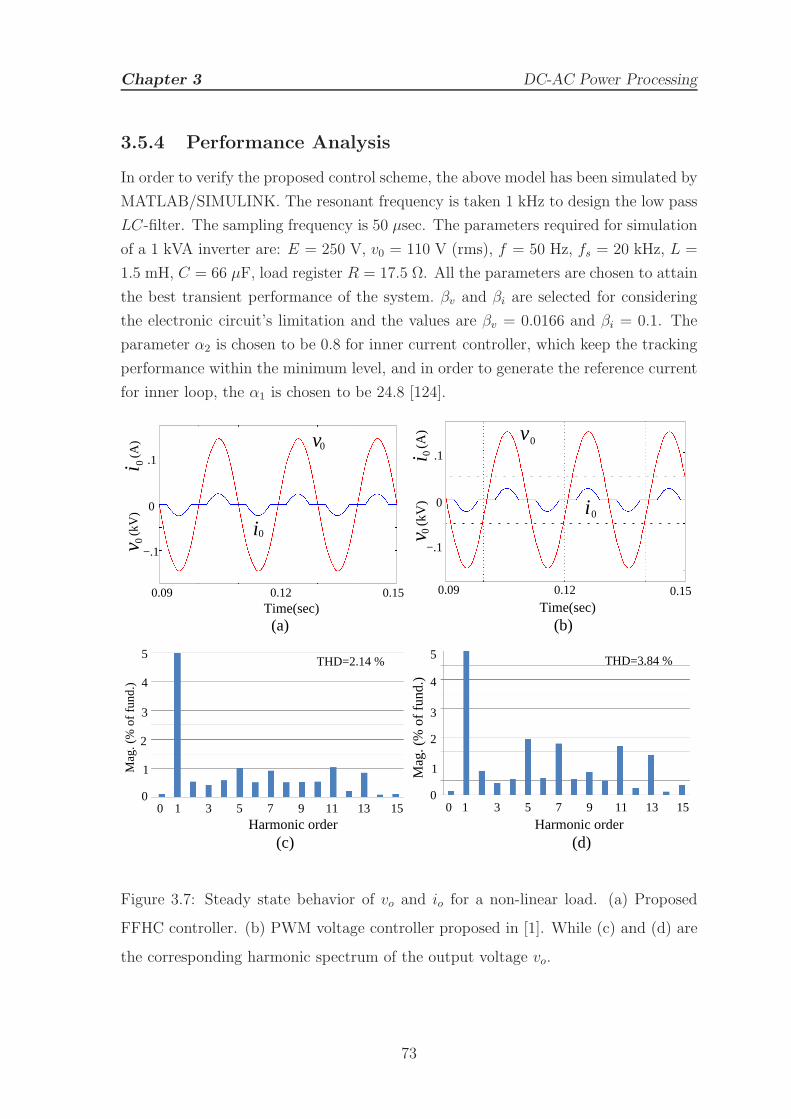
Chapter 3 DC-AC Power Processing
3.5.4 Performance Analysis
In order to verify the proposed control scheme, the above model has been simulated by
MATLAB/SIMULINK. The resonant frequency is taken 1 kHz to design the low pass
LC-filter. The sampling frequency is 50 µsec. The parameters required for simulation
of a 1 kVA inverter are: E = 250 V, v0 = 110 V (rms), f = 50 Hz, fs = 20 kHz, L =
1.5 mH, C = 66 µF, load register R = 17.5 Ω. All the parameters are chosen to attain
the best transient performance of the system. βv and βi are selected for considering
the electronic circuit’s limitation and the values are βv = 0.0166 and βi = 0.1. The
parameter α2 is chosen to be 0.8 for inner current controller, which keep the tracking
performance within the minimum level, and in order to generate the reference current
for inner loop, the α1 is chosen to be 24.8 [124].
0
.1
0.12 0.150.09
−.1
(a)
i 0(A
)0
(kV
) v
i
v
0
0
Time(sec)0.15
0
0.12
−.1
0.09
.1
(kV
) i
(A)
v0
0
0
0 i
v
Time(sec)(b)
0 1 3 5 7 9 11 13 15
4
0
THD=2.14 %
(c)
Mag
. (%
of f
und.
)
5
3
1
2
Harmonic order
THD=3.84 %
Mag
. (%
of f
und.
)
3 5 7 9 11 13 1510
5
4
3
2
0
1
Harmonic order(d)
Figure 3.7: Steady state behavior of vo and io for a non-linear load. (a) Proposed
FFHC controller. (b) PWM voltage controller proposed in [1]. While (c) and (d) are
the corresponding harmonic spectrum of the output voltage vo.
73
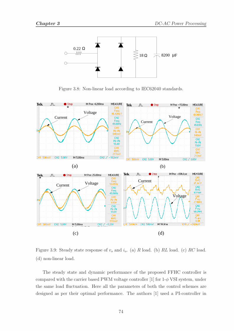
Chapter 3 DC-AC Power Processing
Ω
18 8200 µFΩ
0.22
Figure 3.8: Non-linear load according to IEC62040 standards.
CurrentVoltage
(a) (b)
CurrentVoltage
Current Voltage
(c)
Current
Voltage
(d)
Figure 3.9: Steady state response of vo and io. (a) R load. (b) RL load. (c) RC load.
(d) non-linear load.
The steady state and dynamic performance of the proposed FFHC controller is
compared with the carrier based PWM voltage controller [1] for 1-φ VSI system, under
the same load fluctuation. Here all the parameters of both the control schemes are
designed as per their optimal performance. The authors [1] used a PI-controller in
74
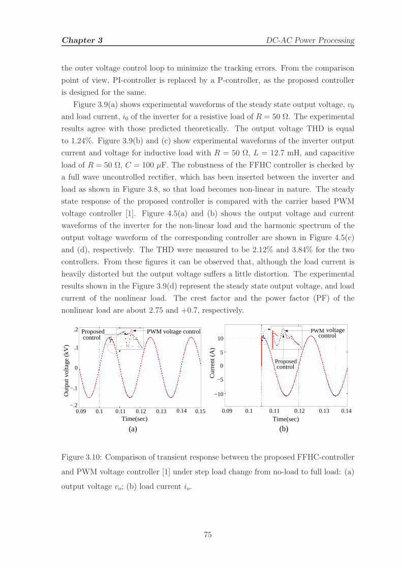
Chapter 3 DC-AC Power Processing
the outer voltage control loop to minimize the tracking errors. From the comparison
point of view, PI-controller is replaced by a P-controller, as the proposed controller
is designed for the same.
Figure 3.9(a) shows experimental waveforms of the steady state output voltage, v0
and load current, i0 of the inverter for a resistive load of R = 50 Ω. The experimental
results agree with those predicted theoretically. The output voltage THD is equal
to 1.24%. Figure 3.9(b) and (c) show experimental waveforms of the inverter output
current and voltage for inductive load with R = 50 Ω, L = 12.7 mH, and capacitive
load of R = 50 Ω, C = 100 µF. The robustness of the FFHC controller is checked by
a full wave uncontrolled rectifier, which has been inserted between the inverter and
load as shown in Figure 3.8, so that load becomes non-linear in nature. The steady
state response of the proposed controller is compared with the carrier based PWM
voltage controller [1]. Figure 4.5(a) and (b) shows the output voltage and current
waveforms of the inverter for the non-linear load and the harmonic spectrum of the
output voltage waveform of the corresponding controller are shown in Figure 4.5(c)
and (d), respectively. The THD were measured to be 2.12% and 3.84% for the two
controllers. From these figures it can be observed that, although the load current is
heavily distorted but the output voltage suffers a little distortion. The experimental
results shown in the Figure 3.9(d) represent the steady state output voltage, and load
current of the nonlinear load. The crest factor and the power factor (PF) of the
nonlinear load are about 2.75 and +0.7, respectively.
(a)
0
PWM voltage controlProposed control
0.09 0.1 0.11 0.12 0.13 0.14 0.15−.2
−.1
.1
.2
Time(sec)
Out
put v
olta
ge (
kV)
0
(b)
10
5
−5
−10
0.10.09 0.11 0.12 0.13 0.14
PWM voltagecontrol
Proposedcontrol
Time(sec)
Cur
rent
(A
)
Figure 3.10: Comparison of transient response between the proposed FFHC-controller
and PWM voltage controller [1] under step load change from no-load to full load: (a)
output voltage vo; (b) load current io.
75
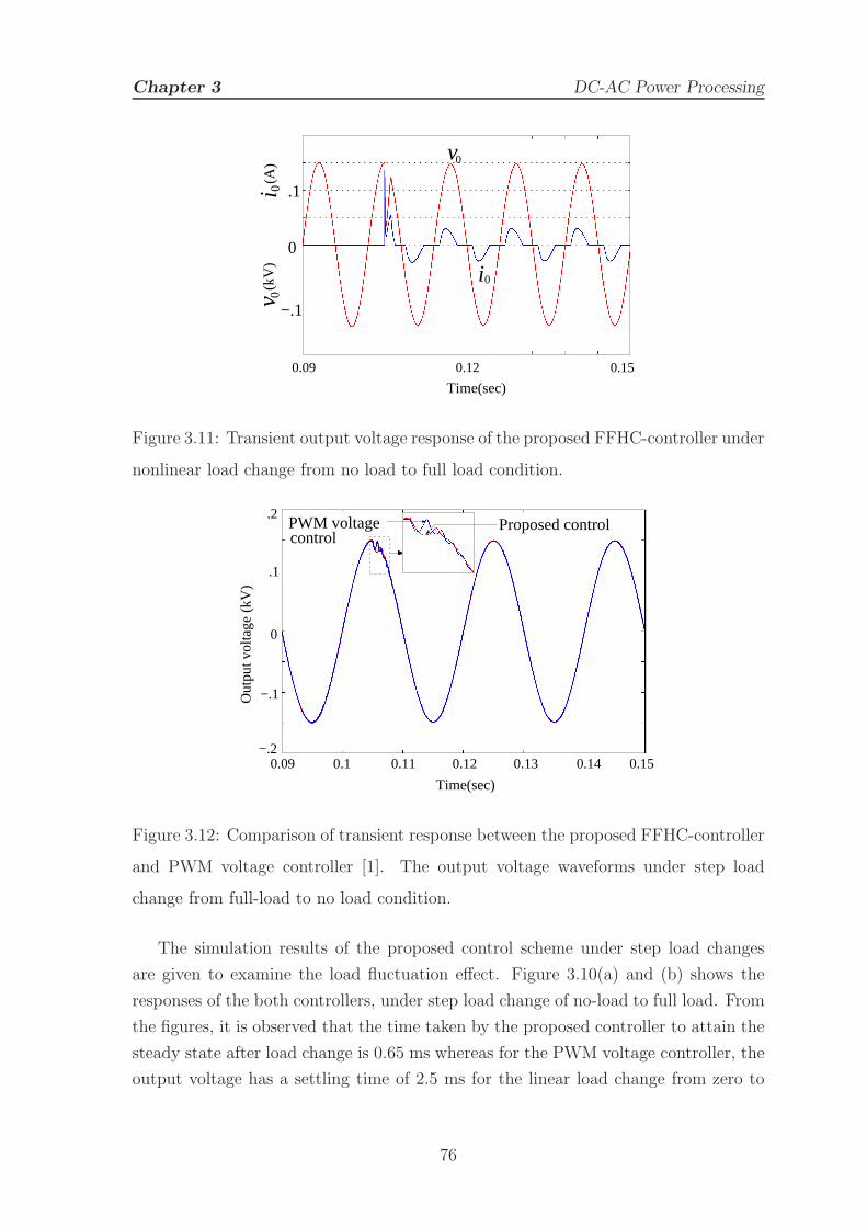
Chapter 3 DC-AC Power Processing
0
−.1
.1
0.150.120.09
i
0 v
00 i(A
)0
v(k
V)
Time(sec)
Figure 3.11: Transient output voltage response of the proposed FFHC-controller under
nonlinear load change from no load to full load condition.
0
Out
put v
olta
ge (
kV)
.2
.1
−.1
−.20.09 0.1 0.11 0.12 0.140.13 0.15
Time(sec)
Proposed controlPWM voltage control
Figure 3.12: Comparison of transient response between the proposed FFHC-controller
and PWM voltage controller [1]. The output voltage waveforms under step load
change from full-load to no load condition.
The simulation results of the proposed control scheme under step load changes
are given to examine the load fluctuation effect. Figure 3.10(a) and (b) shows the
responses of the both controllers, under step load change of no-load to full load. From
the figures, it is observed that the time taken by the proposed controller to attain the
steady state after load change is 0.65 ms whereas for the PWM voltage controller, the
output voltage has a settling time of 2.5 ms for the linear load change from zero to
76
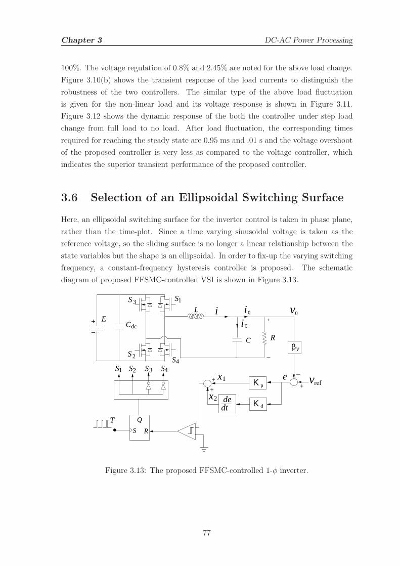
Chapter 3 DC-AC Power Processing
100%. The voltage regulation of 0.8% and 2.45% are noted for the above load change.
Figure 3.10(b) shows the transient response of the load currents to distinguish the
robustness of the two controllers. The similar type of the above load fluctuation
is given for the non-linear load and its voltage response is shown in Figure 3.11.
Figure 3.12 shows the dynamic response of the both the controller under step load
change from full load to no load. After load fluctuation, the corresponding times
required for reaching the steady state are 0.95 ms and .01 s and the voltage overshoot
of the proposed controller is very less as compared to the voltage controller, which
indicates the superior transient performance of the proposed controller.
3.6 Selection of an Ellipsoidal Switching Surface
Here, an ellipsoidal switching surface for the inverter control is taken in phase plane,
rather than the time-plot. Since a time varying sinusoidal voltage is taken as the
reference voltage, so the sliding surface is no longer a linear relationship between the
state variables but the shape is an ellipsoidal. In order to fix-up the varying switching
frequency, a constant-frequency hysteresis controller is proposed. The schematic
diagram of proposed FFSMC-controlled VSI is shown in Figure 3.13.
Κ pvref
Κ d
T
1x
x2 dedt
S
dcC iL
S4
0i 0vE
S2
S3
c
1
vβ RC
Q
21S 3 S4S S
+
+
i
e+
RS
+
−
+
Figure 3.13: The proposed FFSMC-controlled 1-φ inverter.
77
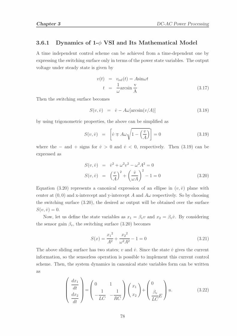
Chapter 3 DC-AC Power Processing
3.6.1 Dynamics of 1-φ VSI and Its Mathematical Model
A time independent control scheme can be achieved from a time-dependent one by
expressing the switching surface only in terms of the power state variables. The output
voltage under steady state is given by
v(t) = vref(t) = Asinωt
t =1
ωarcsin
v
A(3.17)
Then the switching surface becomes
S(v, v) = v −Aω[arcsin(v/A)] (3.18)
by using trigonometric properties, the above can be simplified as
S(v, v) =
[
v ∓ Aω
√
1−( v
A
)]
= 0 (3.19)
where the − and + signs for v > 0 and v < 0, respectively. Then (3.19) can be
expressed as
S(v, v) = v2 + ω2v2 − ω2A2 = 0
S(v, v) =( v
A
)2
+
(v
ωA
)2
− 1 = 0 (3.20)
Equation (3.20) represents a canonical expression of an ellipse in (v, v) plane with
center at (0, 0) and x-intercept and y-intercept A and Aω respectively. So by choosing
the switching surface (3.20), the desired ac output will be obtained over the surface
S(v, v) = 0.
Now, let us define the state variables as x1 = βvv and x2 = βvv. By considering
the sensor gain βv, the switching surface (3.20) becomes
S(x) =x1
2
A2+
x22
ω2A2− 1 = 0 (3.21)
The above sliding surface has two states; v and v. Since the state v gives the current
information, so the sensorless operation is possible to implement this current control
scheme. Then, the system dynamics in canonical state variables form can be written
as
dx1
dt
dx2
dt
=
0 1
−1
LC−
1
RC
(
x1
x2
)
+
0
βv
LCE
u. (3.22)
78

Chapter 3 DC-AC Power Processing
Then for u ∈ (−1, 1), the existence condition and the equivalent control can be
derived as per the Utkin theory [119]. The SMC exists in the vicinity of the switching
surface S(x) if the following local reachability conditions limS(x)→0−dS(x)
dt> 0 and
limS(x)→0+dS(x)
dt< 0, or limS(x)→0
dS(x)
dtS(x) < 0 are simultaneously satisfied. The
existence condition can be derived by simply substituting the time derivative of S(x)
dS(x)
dt=
∂S(x)
∂x
dx
dt=
Jdx
dt> 0 if S(x) < 0
Jdx
dt< 0 if S(x) > 0
(3.23)
into this condition, where J =∂S(x)
∂x=
[
2x1
A2
2x2
(Aω)2
]
. Replacing (3.22) into (3.23)
and applying the control law (3.20), the existence region of SMC can be expressed by
λ1 =2kd
2
A2CRω2x2
[
(LCω2 − 1)
LR.x1 − x2 +
βv.R
LE
]
for u = 1 (3.24)
λ2 =2kd
2
A2CRω2x2
[
(LCω2 − 1)
LR.x1 − x2 −
βv.R
LE
]
for u = −1 (3.25)
where λ1 and λ2 are the boundaries of the existence regions. Unlike [126], both
the above equations are of the second order with parabolic shape. The limiting
boundaries (3.24) and (3.25) give the necessary region of existence region for SMC.
By using the condition S and applying the equivalent control can be found by
ueq =
1
C
dic
dt+
1
LCv − ω2.v
1
LC.E
(3.26)
So, this ueq control assures the feasibility of the SMC over the switching surface S(x, t)
Therefore, after obtaining the mathematical model (3.21) and (3.22) and
constant-frequency switching logic presented, some numerical results are discussed.
3.6.2 Performance Analysis
In order to verify the proposed control scheme, the above model has been simulated by
MATLAB/SIMULINK. The resonant frequency is taken 1 kHz to design the low pass
79
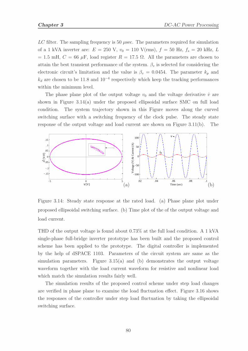
Chapter 3 DC-AC Power Processing
LC filter. The sampling frequency is 50 µsec. The parameters required for simulation
of a 1 kVA inverter are: E = 250 V, v0 = 110 V(rms), f = 50 Hz, fs = 20 kHz, L
= 1.5 mH, C = 66 µF, load register R = 17.5 Ω. All the parameters are chosen to
attain the best transient performance of the system. βv is selected for considering the
electronic circuit’s limitation and the value is βv = 0.0454. The parameter kp and
kd are chosen to be 11.8 and 10−4 respectively which keep the tracking performances
within the minimum level.
The phase plane plot of the output voltage v0 and the voltage derivative v are
shown in Figure 3.14(a) under the proposed ellipsoidal surface SMC on full load
condition. The system trajectory shown in this Figure moves along the curved
switching surface with a switching frequency of the clock pulse. The steady state
response of the output voltage and load current are shown on Figure 3.11(b). The
0 5−5
0
.05
[V]
[V/F
]v
v
−.05
−.1
−.15
.1
.15
(a).02 .04 .06 .08 .1
0
50
100
−50
−100
Time (sec)
Vol
tage
(V
) &
Cur
rent
(A
)v
i 0
(b)
Figure 3.14: Steady state response at the rated load. (a) Phase plane plot under
proposed ellipsoidal switching surface. (b) Time plot of the of the output voltage and
load current.
THD of the output voltage is found about 0.73% at the full load condition. A 1 kVA
single-phase full-bridge inverter prototype has been built and the proposed control
scheme has been applied to the prototype. The digital controller is implemented
by the help of dSPACE 1103. Parameters of the circuit system are same as the
simulation parameters. Figure 3.15(a) and (b) demonstrates the output voltage
waveform together with the load current waveform for resistive and nonlinear load
which match the simulation results fairly well.
The simulation results of the proposed control scheme under step load changes
are verified in phase plane to examine the load fluctuation effect. Figure 3.16 shows
the responses of the controller under step load fluctuation by taking the ellipsoidal
switching surface.
80
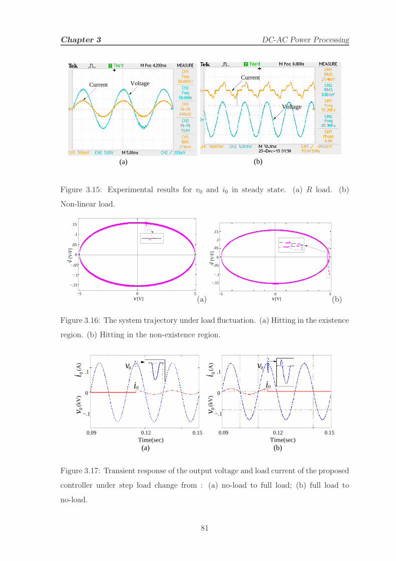
Chapter 3 DC-AC Power Processing
VoltageCurrent
(a)
Current
Voltage
(b)
Figure 3.15: Experimental results for v0 and i0 in steady state. (a) R load. (b)
Non-linear load.
0 5−5
0
−.05
.05
.1
.15
[V]
[V/F
]v
v
−.15
−.1
(a)0 5−5
0
.05
[V]
[V/F
]v
v
.1
.15
−.1
−.15
−.05
(b)
Figure 3.16: The system trajectory under load fluctuation. (a) Hitting in the existence
region. (b) Hitting in the non-existence region.
0
.1
0.12 0.150.09
−.1
(a)
v0
i0
i 0(A
)0
(kV
) v
Time(sec)
0
.1
0.12 0.150.09
−.1
(b)
v0
i0
i 0(A
)0
(kV
) v
Time(sec)
Figure 3.17: Transient response of the output voltage and load current of the proposed
controller under step load change from : (a) no-load to full load; (b) full load to
no-load.
81
Chapter 3 DC-AC Power Processing
The system trajectory defined in (3.21) takes a long time to settle when the
fluctuation occurs at outside of the existence region whereas it will quickly settle
at inside the existence region. Similarly Figure 3.17 shows the dynamic response of
the controller under step load change of no-load to full load and full load to no load
respectively. From the figures, it is observed that the time taken by the proposed
controller to attain the steady state after load change is 0.6 ms and 0.85 ms for the
above two cases.
3.7 Conclusion
In this chapter, two nonlinear current controllers are proposed on the basis of SMC
technique for a 1- φ full bridge VSI. Since SMC produces a huge chattering problem,
so a hysteretic function is employed to generate the switching law for both controllers.
A fixed frequency operation of the inverter is achieved by a simple flip-flop with the
externally driven constant frequency clock pulse. In the first case, the FFHC controller
is implemented through two nested control loops. The outer voltage loop generates the
reference current for the inner current loop. The inner current loop is used to generate
the control pulses for the inverter. However, the second SMC controller has only one
voltage loop. Here the reference voltage is compared with the load voltage and the
error signal is passed through proportional-derivative controller. Since the derivative
of the error signal gives the current information, so no current sensor is required to
implement this control scheme. From the simulation and experimental results, it can
be concluded that both the controller not only give better voltage regulation but also
exhibit good dynamic performance under sudden load fluctuation. For the sake of
simplicity, it has taken a dc voltage source as the inverter input supply. Moreover,
these control scheme are also applicable to the islanded distribution generation (DG)
system, powered by the renewable energy sources like pv system, fuel cell system etc.
82
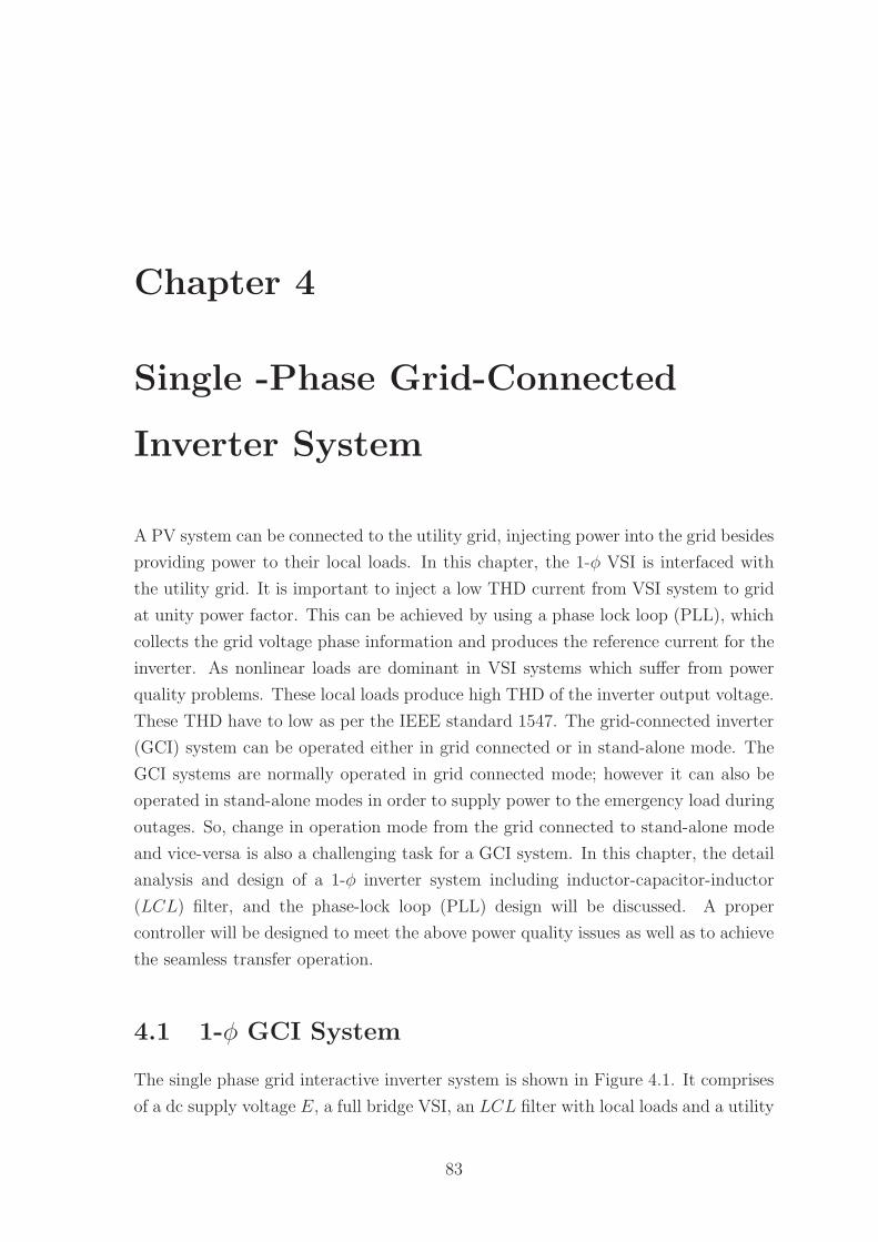
Chapter 4
Single -Phase Grid-Connected
Inverter System
A PV system can be connected to the utility grid, injecting power into the grid besides
providing power to their local loads. In this chapter, the 1-φ VSI is interfaced with
the utility grid. It is important to inject a low THD current from VSI system to grid
at unity power factor. This can be achieved by using a phase lock loop (PLL), which
collects the grid voltage phase information and produces the reference current for the
inverter. As nonlinear loads are dominant in VSI systems which suffer from power
quality problems. These local loads produce high THD of the inverter output voltage.
These THD have to low as per the IEEE standard 1547. The grid-connected inverter
(GCI) system can be operated either in grid connected or in stand-alone mode. The
GCI systems are normally operated in grid connected mode; however it can also be
operated in stand-alone modes in order to supply power to the emergency load during
outages. So, change in operation mode from the grid connected to stand-alone mode
and vice-versa is also a challenging task for a GCI system. In this chapter, the detail
analysis and design of a 1-φ inverter system including inductor-capacitor-inductor
(LCL) filter, and the phase-lock loop (PLL) design will be discussed. A proper
controller will be designed to meet the above power quality issues as well as to achieve
the seamless transfer operation.
4.1 1-φ GCI System
The single phase grid interactive inverter system is shown in Figure 4.1. It comprises
of a dc supply voltage E, a full bridge VSI, an LCL filter with local loads and a utility
83
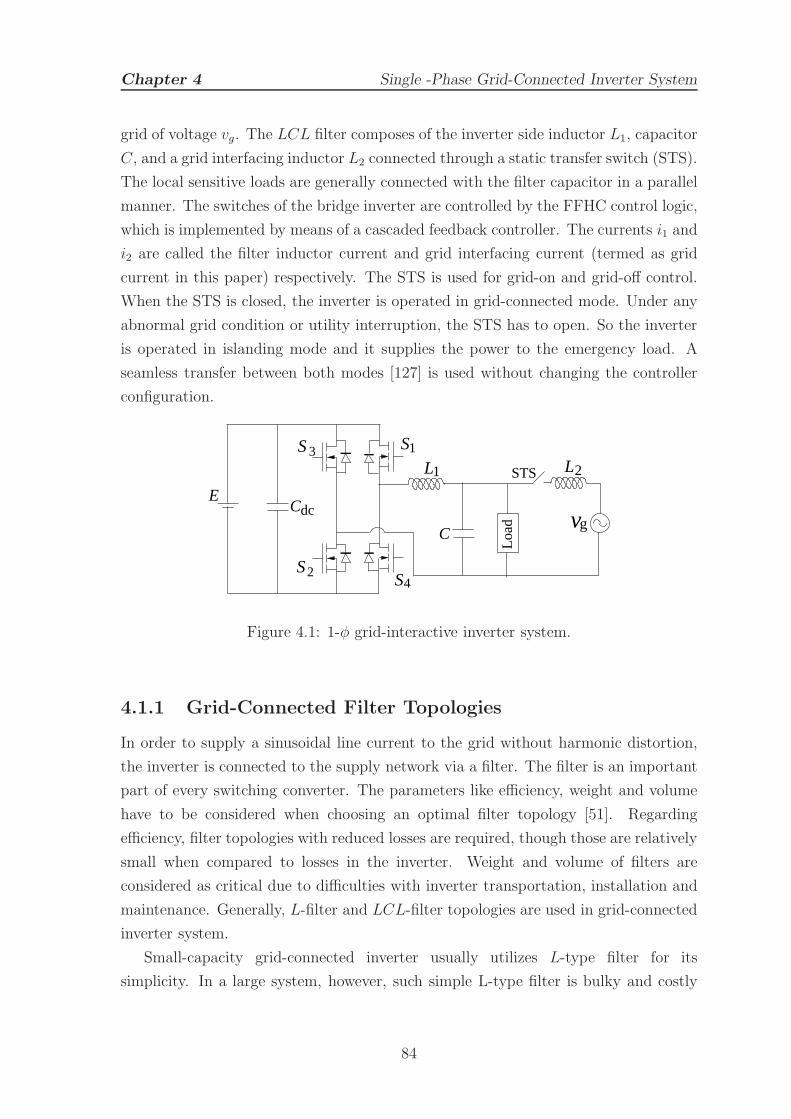
Chapter 4 Single -Phase Grid-Connected Inverter System
grid of voltage vg. The LCL filter composes of the inverter side inductor L1, capacitor
C, and a grid interfacing inductor L2 connected through a static transfer switch (STS).
The local sensitive loads are generally connected with the filter capacitor in a parallel
manner. The switches of the bridge inverter are controlled by the FFHC control logic,
which is implemented by means of a cascaded feedback controller. The currents i1 and
i2 are called the filter inductor current and grid interfacing current (termed as grid
current in this paper) respectively. The STS is used for grid-on and grid-off control.
When the STS is closed, the inverter is operated in grid-connected mode. Under any
abnormal grid condition or utility interruption, the STS has to open. So the inverter
is operated in islanding mode and it supplies the power to the emergency load. A
seamless transfer between both modes [127] is used without changing the controller
configuration.
S
S4S2
S3 1
Cdc
L L
C
1 2STS
Load
E
vg
Figure 4.1: 1-φ grid-interactive inverter system.
4.1.1 Grid-Connected Filter Topologies
In order to supply a sinusoidal line current to the grid without harmonic distortion,
the inverter is connected to the supply network via a filter. The filter is an important
part of every switching converter. The parameters like efficiency, weight and volume
have to be considered when choosing an optimal filter topology [51]. Regarding
efficiency, filter topologies with reduced losses are required, though those are relatively
small when compared to losses in the inverter. Weight and volume of filters are
considered as critical due to difficulties with inverter transportation, installation and
maintenance. Generally, L-filter and LCL-filter topologies are used in grid-connected
inverter system.
Small-capacity grid-connected inverter usually utilizes L-type filter for its
simplicity. In a large system, however, such simple L-type filter is bulky and costly
84
Chapter 4 Single -Phase Grid-Connected Inverter System
due to the large current capability. Although this topology has one inductor only,
the system dynamics is poor due to the voltage drop across the inductor causing long
time responses. Moreover, the inverter switching frequency must be high to attenuate
the switching harmonics [51], [128]. Compared to L-type filter, the same amount of
switching ripple reduction can be achieved with smaller inductors by the LCL filter. In
summary, compared to the L-filter, the LCL-filter configuration allows more flexible
inverter usage and also provides more attenuation of switching ripple. However, it
is more complicated when using the LCL-filter; many design considerations, like the
location of current feedback selections and component selections, need to be taken
into account.
Two different current feedback schemes are possible to use; inverter side
inductor current feedback and grid side inductor current feedback. In terms of
the low-frequency characteristics, both of the two feedback schemes almost have no
difference. This is because the reactance of the filter capacitor is very large at low
frequency such that the inverter side current is approximately equal to the grid side
current, except for the switching frequency ripples. Nevertheless, once considering
the high-frequency characteristics of the two feedback schemes, particularly the LC
resonance, these two current feedback schemes will become totally different. In order
to optimally design the LCL-filter to achieve lowest cost size, it is also necessary to
examine both of the two feedback schemes respectively.
The design procedure of the LCL filter is described as following. First, the
selection of the inverter-side inductor L1 should compromise the output current
performance, system cost, size, and efficiency. For example, with a higher L1 value,
lower current ripple can be obtained and a higher controller gain can be designed to
obtain better current performance. However, a higher inductance value requires higher
cost and occupies a larger volume. For the efficiency concern, higher inductance allows
lower current ripple in the inductor L1, which decreases core losses of the inductor.
On the other hand, higher inductance value increases the winding loss for longer wire
required.
The selection of capacitor value depends on the application of inverters. If the
inverters are used for only grid-connected applications, the selection of C can be
determined by limiting the reactive power consumed in C [129]. It is noteworthy that
the selection of higher capacitance, the more reactive power is circulating between the
inverter and the capacitor, which decreases the inverter efficiency. On the other hand,
the selection of the filter capacitor in standalone mode will be determined by the
required voltage ripple damping because the inverter-side inductor L1 and the filter
capacitor C will form a second-order filter that provides a -40dB/dec attenuation after
85
Chapter 4 Single -Phase Grid-Connected Inverter System
the resonant frequency of this L1 − C filter.
Calculation of The grid-side inductor value can be calculated from the resonance
frequency of the LCL filter based on the requirement for grid-current switching
ripple attenuation. The value of L2 can also be found from the inverter to grid
side inductance factor [130], [51].
The value of L1, L2, and C can be found from the following
expressions [130], [51], [129]
L1 =E
16fs∆i1, L2 = rL1, C = 0.05
P
ωgvg(4.1)
where E, fs, ∆i1, and r are the dc input voltage, switching frequency, allowable ripple
current through L1, and inverter to grid side inductance factor respectively.
4.2 State-of-the-Art of Current Controllers
The GCI systems can be operated either in grid-connected or in stand-alone mode.
The GCI systems are normally operated in grid-connected mode; however it can also
be operated in stand-alone modes in order to supply power to the emergency load
during outages. Generally, the inverters connected in the micro-grid act as current
sources in grid-connected mode and as voltage sources in islanded mode [131]. This
comprises the change of the controller configuration with the change of operation from
the grid-connected to islanded mode and vice-versa [127]. When inverters are operated
as voltage sources, then the change of the controller is not required by changing the
operational mode. Many Seamless transfer controllers were proposed by changing the
references of the controllers without changing controller structure [132]. All the above
controllers have parallel control structure comprising of a grid side current controller
and an output voltage controller. The active and reactive power controls are two
important aspects of the grid-connected inverters or micro-grid [133].
As nonlinear loads are the dominant in distributed generation (DG) systems, the
micro-grid suffers by power quality problems [134]. These local loads produce high
total harmonic distortion (THD) of the inverter output voltage as well as the current
exchanged from inverter to grid. These THD have to low as per the IEEE standard
1547. Many literatures were reported to obtain low load voltage THD [135] or low grid
side current THD [136] in the grid-connected system. However, hardly any control
strategy has been proposed to achieve the low THD of the grid current and inverter
load voltage simultaneously. A nested control structure comprising of a current and
86

Chapter 4 Single -Phase Grid-Connected Inverter System
voltage control loops is proposed in this paper to overcome the above problems. The
outer current controller in grid side is used for the power quality of the grid current;
whereas the voltage controller is used for the power quality of the inverter output
voltage. The LCL filter used in the system can be split into two separate parts.
The LC filter part is required to design the voltage controller loops whereas the
grid interfacing inductor L is required to design the outer current controller. All the
controllers are implemented in the stationary reference frame.
It is notable stressing that the proposed cascaded control structure improves the
dynamic response, power quality of both inverter load voltage and the grid current and
attains the seamless transfer operation. In the recent past, several control strategies
have been reported like conventional PI controller [137], proportional-resonant (PR)
controller [138], deadbeat controller [139], repetitive controller [140], to fulfill the
aforesaid requirements. However, these linear controllers can only fulfill partially. On
the other hand, as a non-linear control scheme, namely, sliding mode control (SMC)
has commonly been used in grid-connected inverter system since it is well known for
its robustness, guaranteed stability and good dynamic response over wide range of
operating conditions [141]. The SMC utilizes a switching control law to drive the
state trajectory from any initial positions to a specified surface in the state space
called sliding or switching surface, and maintain it on this surface for all subsequent
time [119]. However, SMC operates at variable switching frequency at which an
undesirable chattering phenomenon may occur. In order to compensate the above
drawback partially, the SMC are realized by means of a hysteresis comparator [120],
which also provides a variable switching frequency. So, it produces an undesired
harmonic spectrum, for which, designing of the filter components is very difficult.
Several authors have proposed constant frequency SMC by means of a variable
width hysteresis controller [121], which can however lead to a complex analog
implementation, thereby involve more cost. Moreover, the width of hysteresis band
depends on the converter parameters. Alternatively, fixed frequency SMC can also be
achieved by comparing an external ramp signal to the switching surface [122]. But,
the switching instant for these controllers does not depend on the switching surface
behavior.
In this work, a cascaded SMC scheme is proposed to improve the dynamic response
of a 1-φ inverter subjected to a sudden fluctuation of load. The proposed controller is
designed on the basis of SMC technique. A hysteresis band is employed to generate
the switching law for the inverter circuit and that has been implemented using a
simple flip-flop with externally driven constant frequency clock pulses. In spite of this
constant frequency switching operation, it also retains all of the properties of an ideal
87
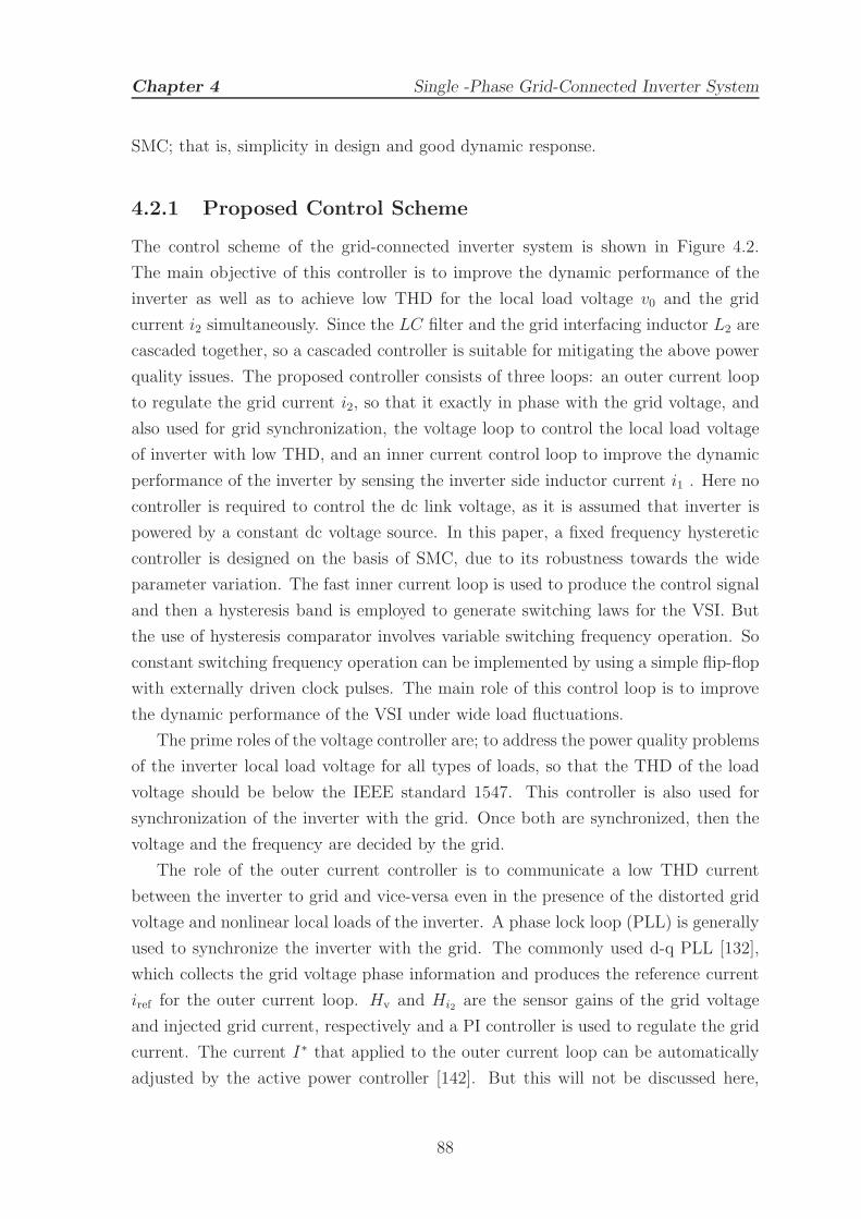
Chapter 4 Single -Phase Grid-Connected Inverter System
SMC; that is, simplicity in design and good dynamic response.
4.2.1 Proposed Control Scheme
The control scheme of the grid-connected inverter system is shown in Figure 4.2.
The main objective of this controller is to improve the dynamic performance of the
inverter as well as to achieve low THD for the local load voltage v0 and the grid
current i2 simultaneously. Since the LC filter and the grid interfacing inductor L2 are
cascaded together, so a cascaded controller is suitable for mitigating the above power
quality issues. The proposed controller consists of three loops: an outer current loop
to regulate the grid current i2, so that it exactly in phase with the grid voltage, and
also used for grid synchronization, the voltage loop to control the local load voltage
of inverter with low THD, and an inner current control loop to improve the dynamic
performance of the inverter by sensing the inverter side inductor current i1 . Here no
controller is required to control the dc link voltage, as it is assumed that inverter is
powered by a constant dc voltage source. In this paper, a fixed frequency hysteretic
controller is designed on the basis of SMC, due to its robustness towards the wide
parameter variation. The fast inner current loop is used to produce the control signal
and then a hysteresis band is employed to generate switching laws for the VSI. But
the use of hysteresis comparator involves variable switching frequency operation. So
constant switching frequency operation can be implemented by using a simple flip-flop
with externally driven clock pulses. The main role of this control loop is to improve
the dynamic performance of the VSI under wide load fluctuations.
The prime roles of the voltage controller are; to address the power quality problems
of the inverter local load voltage for all types of loads, so that the THD of the load
voltage should be below the IEEE standard 1547. This controller is also used for
synchronization of the inverter with the grid. Once both are synchronized, then the
voltage and the frequency are decided by the grid.
The role of the outer current controller is to communicate a low THD current
between the inverter to grid and vice-versa even in the presence of the distorted grid
voltage and nonlinear local loads of the inverter. A phase lock loop (PLL) is generally
used to synchronize the inverter with the grid. The commonly used d-q PLL [132],
which collects the grid voltage phase information and produces the reference current
iref for the outer current loop. Hv and Hi2 are the sensor gains of the grid voltage
and injected grid current, respectively and a PI controller is used to regulate the grid
current. The current I∗ that applied to the outer current loop can be automatically
adjusted by the active power controller [142]. But this will not be discussed here,
88
Chapter 4 Single -Phase Grid-Connected Inverter System
PLL
i
E
Q
SR
S
gH
v
i1H 2H
Inve
rter
Brid
ge
Load
+
Gate Driver
ref
uiv
S
T i−
−
−
+
i ∗
+
++
i i2L1
g
21
K1
2K
s+ KiKp
Hv
ref
L
C
I ∗θ
ie
+
−
Figure 4.2: Overall control diagram of a 1-φ grid-connected inverter system.
so the current reference amplitude I∗ is directly given here. The output of the grid
current controller ui, which represents the variation of the grid voltage due to the
voltage drop across the grid inductor L2 , is added to the grid voltage to generate the
reference for the load voltage.
In this paper, a fixed frequency hysteretic controller is designed on the basis of
SMC, due to its robustness towards the wide parameter variation.
4.3 SMC in Grid-Connected Inverter System
Normally, SMC is considered as a good alternative to control of switching converters.
The main advantages of such control scheme over classical one are; its robustness,
and high dynamics performances under parameter fluctuations. However, in order
to achieve these advantages, the power electronics practitioners usually design and
implement the SMC on the basis of hysteresis controller with a band. The hysteresis
band essentially forms the boundary layers of the switching surface. Within these
boundaries the trajectory (i.e., current and voltage) of the systems jitters and travel
along the switching surface guided by boundary layers. The detailed analysis of
proposed cascaded SMC was described here, followed by the dynamical model of
grid-connected inverter system.
89
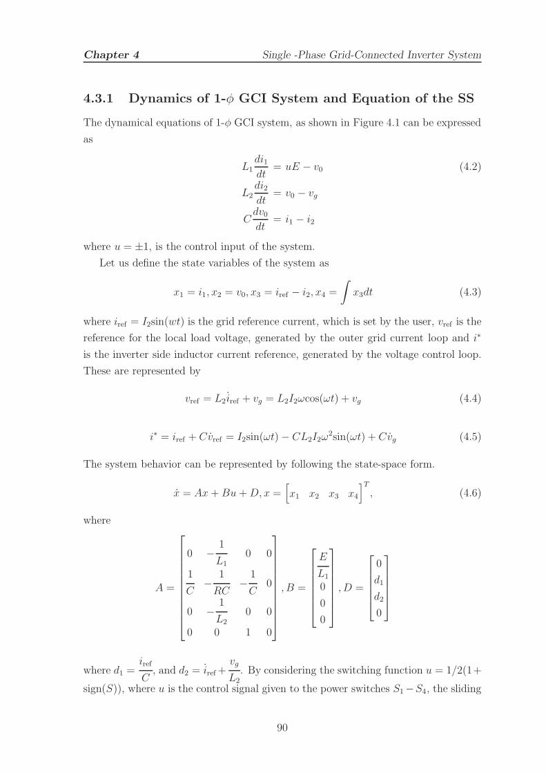
Chapter 4 Single -Phase Grid-Connected Inverter System
4.3.1 Dynamics of 1-φ GCI System and Equation of the SS
The dynamical equations of 1-φ GCI system, as shown in Figure 4.1 can be expressed
as
L1di1dt
= uE − v0 (4.2)
L2di2dt
= v0 − vg
Cdv0dt
= i1 − i2
where u = ±1, is the control input of the system.
Let us define the state variables of the system as
x1 = i1, x2 = v0, x3 = iref − i2, x4 =
∫
x3dt (4.3)
where iref = I2sin(wt) is the grid reference current, which is set by the user, vref is the
reference for the local load voltage, generated by the outer grid current loop and i∗
is the inverter side inductor current reference, generated by the voltage control loop.
These are represented by
vref = L2iref + vg = L2I2ωcos(ωt) + vg (4.4)
i∗ = iref + Cvref = I2sin(ωt)− CL2I2ω2sin(ωt) + Cvg (4.5)
The system behavior can be represented by following the state-space form.
x = Ax+Bu+D, x =[
x1 x2 x3 x4
]T
, (4.6)
where
A =
0 −1
L10 0
1
C−
1
RC−
1
C0
0 −1
L20 0
0 0 1 0
, B =
E
L1
0
0
0
, D =
0
d1
d2
0
where d1 =iref
C, and d2 = iref+
vg
L2
. By considering the switching function u = 1/2(1+
sign(S)), where u is the control signal given to the power switches S1−S4, the sliding
90

Chapter 4 Single -Phase Grid-Connected Inverter System
surface of the proposed cascaded controller is chosen by the linear combination of the
state variables, i.e
S(x, t) = −K1x1 −K1K2x2 +K1K2Kpx3 +K1K2Kpx4 (4.7)
or,
S(x, t) = α1x1 + α2x2 + α3x3 + α4x4 (4.8)
where α1 = -K1, α2 = -K1K2, α3 = K1K2Kp, and α4 = K1K2Ki are called sliding
coefficients.
4.3.2 Existence Condition
The three necessary conditions for SMC operation are hitting, existence, and stability
conditions. The hitting condition has been discussed till now, by selecting the suitable
switching function. As far as existence condition, the SMC exists in the vicinity of an
sliding surface S(x), if the following local reachability conditions limS(x)→0−dS(x)dt
<0
or limS(x)→0+dS(x)
dt>0 are simultaneously satisfied [119]. The reachability condition
can be derived by simply substituting the time derivative of S(x)
dS(x)
dt=
∂S(x)
∂t
dx
dt=
Jdx
dt> 0 for S(x) < 0
Jdx
dt< 0 for S(x) > 0
(4.9)
into this condition, where J =∂S(x)
∂t=[
α1 α2 α3 α4
]
. Replacing (4.6) into (4.9),
and applying the control law (4.8), the existence region of SMC can be expressed as
λ1 = x1
(
−α1
L1+
α2
C
)
+ x2
(
− α2
RC− α3
L2
)
+ x3
(
−α2
C
)
+α1E
L1+α2d1 +α3d2 (4.10)
λ2 = x1
(
−α1
L1+
α2
C
)
+ x2
(
− α2
RC− α3
L2
)
+ x3
(
−α2
C
)
− α1E
L1+ α2d1 +α3d2 (4.11)
The limiting boundaries (4.10) and (4.11) give the necessary region of existence for
the SMC on smooth sliding surface [119] and set the design range for the sliding
coefficients, which should ensure the system to remain in sliding mode operation
when the system trajectory is close to the sliding surface.
91
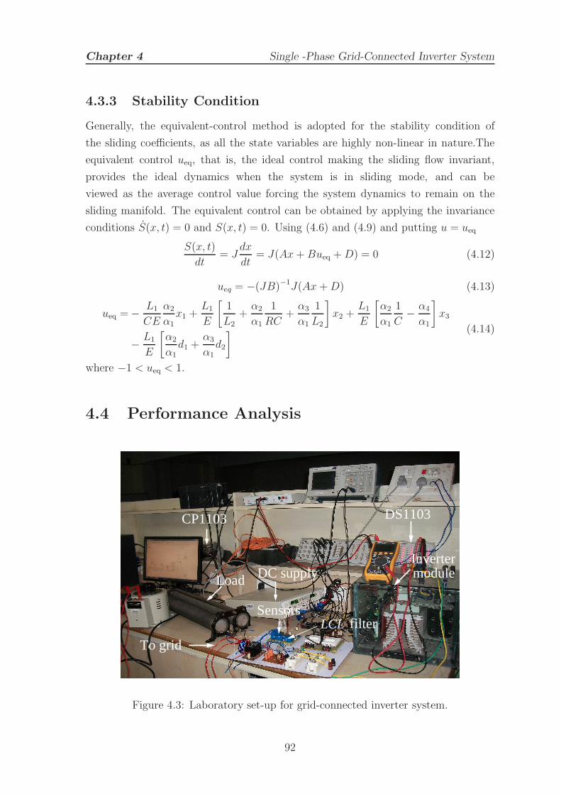
Chapter 4 Single -Phase Grid-Connected Inverter System
4.3.3 Stability Condition
Generally, the equivalent-control method is adopted for the stability condition of
the sliding coefficients, as all the state variables are highly non-linear in nature.The
equivalent control ueq, that is, the ideal control making the sliding flow invariant,
provides the ideal dynamics when the system is in sliding mode, and can be
viewed as the average control value forcing the system dynamics to remain on the
sliding manifold. The equivalent control can be obtained by applying the invariance
conditions S(x, t) = 0 and S(x, t) = 0. Using (4.6) and (4.9) and putting u = ueq
S(x, t)
dt= J
dx
dt= J(Ax+Bueq +D) = 0 (4.12)
ueq = −(JB)−1J(Ax+D) (4.13)
ueq =− L1
CE
α2
α1
x1 +L1
E
[1
L2
+α2
α1
1
RC+
α3
α1
1
L2
]
x2 +L1
E
[α2
α1
1
C− α4
α1
]
x3
− L1
E
[α2
α1d1 +
α3
α1d2
] (4.14)
where −1 < ueq < 1.
4.4 Performance Analysis
Load
LCLSensors
module
filter
DC supplyInverter
DS1103
To grid
CP1103
Figure 4.3: Laboratory set-up for grid-connected inverter system.
92
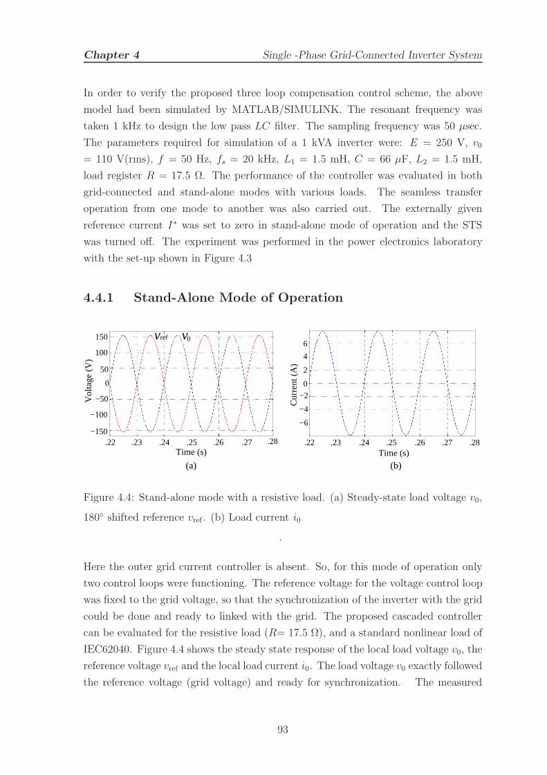
Chapter 4 Single -Phase Grid-Connected Inverter System
In order to verify the proposed three loop compensation control scheme, the above
model had been simulated by MATLAB/SIMULINK. The resonant frequency was
taken 1 kHz to design the low pass LC filter. The sampling frequency was 50 µsec.
The parameters required for simulation of a 1 kVA inverter were: E = 250 V, v0
= 110 V(rms), f = 50 Hz, fs = 20 kHz, L1 = 1.5 mH, C = 66 µF, L2 = 1.5 mH,
load register R = 17.5 Ω. The performance of the controller was evaluated in both
grid-connected and stand-alone modes with various loads. The seamless transfer
operation from one mode to another was also carried out. The externally given
reference current I∗ was set to zero in stand-alone mode of operation and the STS
was turned off. The experiment was performed in the power electronics laboratory
with the set-up shown in Figure 4.3
4.4.1 Stand-Alone Mode of Operation
vvref 0
0
.23.22 .24 .25 .26 .27 .28Time (s)
150
100
50
−50
−100
−150
(a)
Vol
tage
(V
)
(b)
.22 .23 .24 .25 .26 .27 .28Time (s)
6
4
2
0
−2
−4
−6
Cur
rent
(A
)
Figure 4.4: Stand-alone mode with a resistive load. (a) Steady-state load voltage v0,
180 shifted reference vref . (b) Load current i0
.
Here the outer grid current controller is absent. So, for this mode of operation only
two control loops were functioning. The reference voltage for the voltage control loop
was fixed to the grid voltage, so that the synchronization of the inverter with the grid
could be done and ready to linked with the grid. The proposed cascaded controller
can be evaluated for the resistive load (R= 17.5 Ω), and a standard nonlinear load of
IEC62040. Figure 4.4 shows the steady state response of the local load voltage v0, the
reference voltage vref and the local load current i0. The load voltage v0 exactly followed
the reference voltage (grid voltage) and ready for synchronization. The measured
93
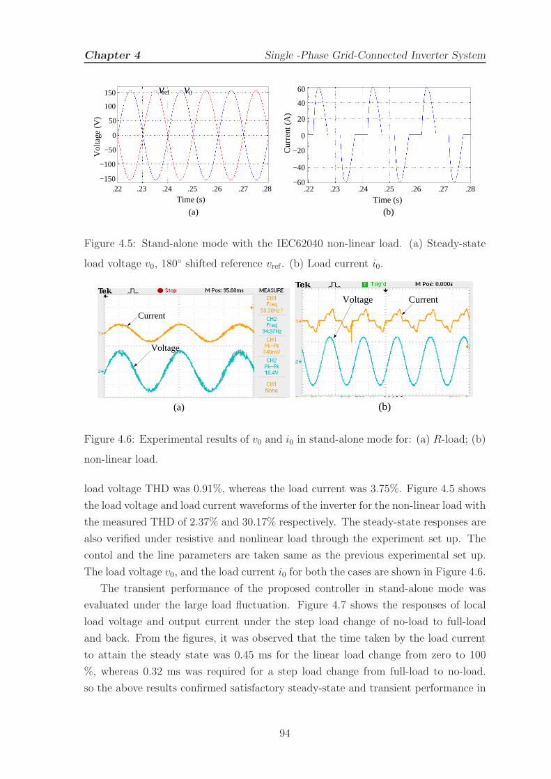
Chapter 4 Single -Phase Grid-Connected Inverter System
refv v0
(a)
.28.27.26.25.24.23.22
150
100
0
−50
−100
−150
Time (s)
Vol
tage
(V
)
50
Time (s)
60
40
20
0
−20
−40
−60.22 .23 .24 .25 .26 .27 .28
(b)
Cur
rent
(A
)
Figure 4.5: Stand-alone mode with the IEC62040 non-linear load. (a) Steady-state
load voltage v0, 180 shifted reference vref . (b) Load current i0.
(a)
Voltage
Current
Current
(b)
Voltage
Figure 4.6: Experimental results of v0 and i0 in stand-alone mode for: (a) R-load; (b)
non-linear load.
load voltage THD was 0.91%, whereas the load current was 3.75%. Figure 4.5 shows
the load voltage and load current waveforms of the inverter for the non-linear load with
the measured THD of 2.37% and 30.17% respectively. The steady-state responses are
also verified under resistive and nonlinear load through the experiment set up. The
contol and the line parameters are taken same as the previous experimental set up.
The load voltage v0, and the load current i0 for both the cases are shown in Figure 4.6.
The transient performance of the proposed controller in stand-alone mode was
evaluated under the large load fluctuation. Figure 4.7 shows the responses of local
load voltage and output current under the step load change of no-load to full-load
and back. From the figures, it was observed that the time taken by the load current
to attain the steady state was 0.45 ms for the linear load change from zero to 100
%, whereas 0.32 ms was required for a step load change from full-load to no-load.
so the above results confirmed satisfactory steady-state and transient performance in
94
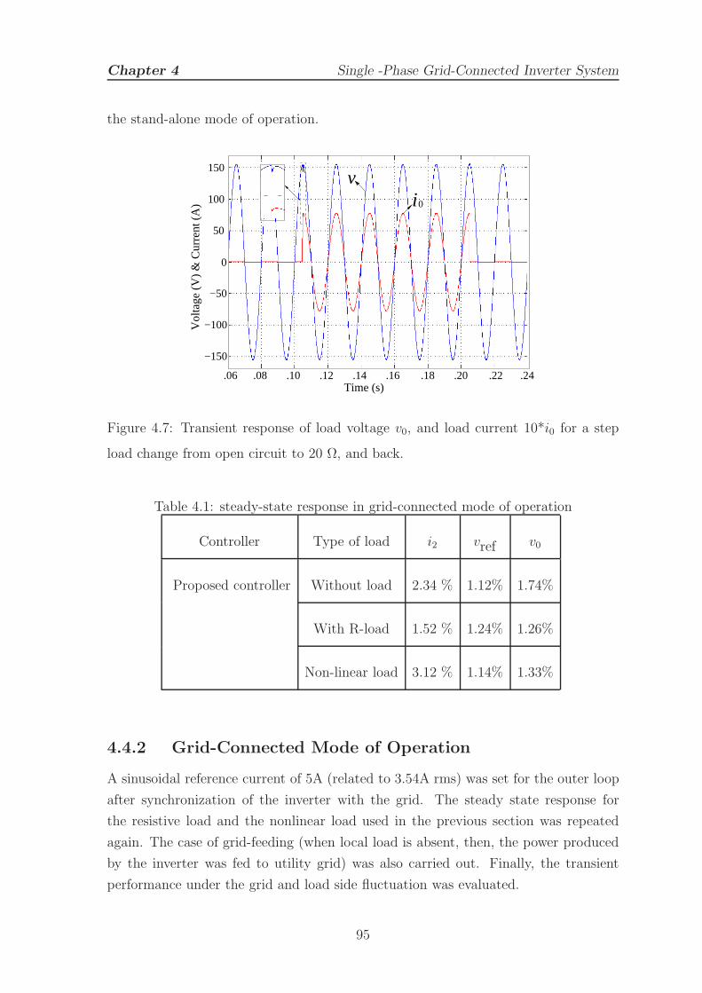
Chapter 4 Single -Phase Grid-Connected Inverter System
the stand-alone mode of operation.
.24
0
.08 .10 .14 .16 .18 .20 .22
150
100
50
−50
−100
−150
vi 0
.06Time (s)
.12
Vol
tage
(V
) &
Cur
rent
(A
)
Figure 4.7: Transient response of load voltage v0, and load current 10*i0 for a step
load change from open circuit to 20 Ω, and back.
Table 4.1: steady-state response in grid-connected mode of operation
Controller Type of load i2 vref v0
Proposed controller Without load 2.34 % 1.12% 1.74%
With R-load 1.52 % 1.24% 1.26%
Non-linear load 3.12 % 1.14% 1.33%
4.4.2 Grid-Connected Mode of Operation
A sinusoidal reference current of 5A (related to 3.54A rms) was set for the outer loop
after synchronization of the inverter with the grid. The steady state response for
the resistive load and the nonlinear load used in the previous section was repeated
again. The case of grid-feeding (when local load is absent, then, the power produced
by the inverter was fed to utility grid) was also carried out. Finally, the transient
performance under the grid and load side fluctuation was evaluated.
95
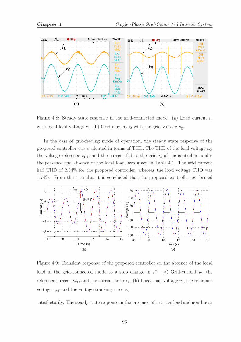
Chapter 4 Single -Phase Grid-Connected Inverter System
i0
v0
(a)
i
vg
2
(b)
Figure 4.8: Steady state response in the grid-connected mode. (a) Load current i0
with local load voltage v0. (b) Grid current i2 with the grid voltage vg.
In the case of grid-feeding mode of operation, the steady state response of the
proposed controller was evaluated in terms of THD. The THD of the load voltage v0,
the voltage reference vref , and the current fed to the grid i2 of the controller, under
the presence and absence of the local load, was given in Table 4.1. The grid current
had THD of 2.34% for the proposed controller, whereas the load voltage THD was
1.74%. From these results, it is concluded that the proposed controller performed
(a)
Cur
rent
(A
)
.06 .08 .10 .12 .14 .16
−8
−4
4
8
0
iref i2
50*ei
Time (s).16.14.12.10.08.06
150
100
Vol
tage
(V
)
50
0
−50
−100
−150
(b)
Time (s)
Figure 4.9: Transient response of the proposed controller on the absence of the local
load in the grid-connected mode to a step change in I∗. (a) Grid-current i2, the
reference current iref , and the current error ei. (b) Local load voltage v0, the reference
voltage vref and the voltage tracking error ev.
satisfactorily. The steady state response in the presence of resistive load and non-linear
96
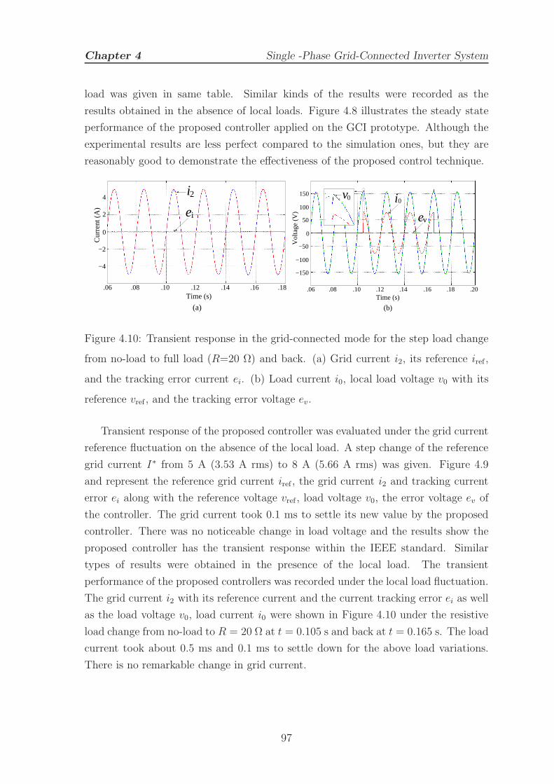
Chapter 4 Single -Phase Grid-Connected Inverter System
load was given in same table. Similar kinds of the results were recorded as the
results obtained in the absence of local loads. Figure 4.8 illustrates the steady state
performance of the proposed controller applied on the GCI prototype. Although the
experimental results are less perfect compared to the simulation ones, but they are
reasonably good to demonstrate the effectiveness of the proposed control technique.
(a)
Cur
rent
(A
)
.18.16.14.12.10.08.06
4
2
0
−2
−4
Time (s)
2i
ei
(b)
Time (s).20.18.16.14.12.08.06
150
100
Vol
tage
(V
)
50
0
−100
−50
−150
.10
i0
ev
v0
Figure 4.10: Transient response in the grid-connected mode for the step load change
from no-load to full load (R=20 Ω) and back. (a) Grid current i2, its reference iref ,
and the tracking error current ei. (b) Load current i0, local load voltage v0 with its
reference vref , and the tracking error voltage ev.
Transient response of the proposed controller was evaluated under the grid current
reference fluctuation on the absence of the local load. A step change of the reference
grid current I∗ from 5 A (3.53 A rms) to 8 A (5.66 A rms) was given. Figure 4.9
and represent the reference grid current iref , the grid current i2 and tracking current
error ei along with the reference voltage vref , load voltage v0, the error voltage ev of
the controller. The grid current took 0.1 ms to settle its new value by the proposed
controller. There was no noticeable change in load voltage and the results show the
proposed controller has the transient response within the IEEE standard. Similar
types of results were obtained in the presence of the local load. The transient
performance of the proposed controllers was recorded under the local load fluctuation.
The grid current i2 with its reference current and the current tracking error ei as well
as the load voltage v0, load current i0 were shown in Figure 4.10 under the resistive
load change from no-load to R = 20 Ω at t = 0.105 s and back at t = 0.165 s. The load
current took about 0.5 ms and 0.1 ms to settle down for the above load variations.
There is no remarkable change in grid current.
97
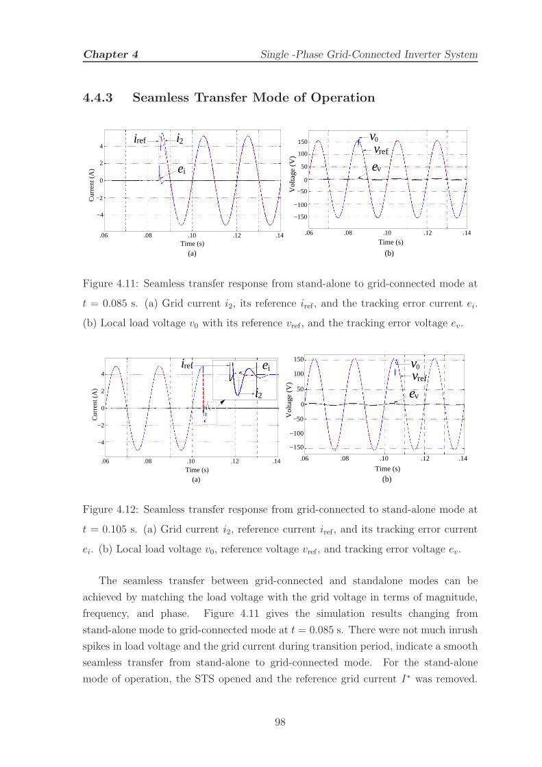
Chapter 4 Single -Phase Grid-Connected Inverter System
4.4.3 Seamless Transfer Mode of Operation
0
2
4
−2
−4
Cur
rent
(A
)
.06 .08 .10 .12 .14Time (s)
(a)
ii 2
e
ref
i
150
100
50
0
−100
−150
−50
.10 .12 .14.08.06
Time (s)
(b)
Vol
tage
(V
)
v0
refvev
Figure 4.11: Seamless transfer response from stand-alone to grid-connected mode at
t = 0.085 s. (a) Grid current i2, its reference iref , and the tracking error current ei.
(b) Local load voltage v0 with its reference vref , and the tracking error voltage ev.
.06 .08 .10 .12 .14
Time (s)
(a)
0
4
2
−4
−2
Cur
rent
(A
)
iref
2
i
i
e
(b)
−150
−100
−50
0
50
100
150
.10 .12 .14.06 .08
Vol
tage
(V
)
Time (s)
v0
vref
ev
Figure 4.12: Seamless transfer response from grid-connected to stand-alone mode at
t = 0.105 s. (a) Grid current i2, reference current iref , and its tracking error current
ei. (b) Local load voltage v0, reference voltage vref , and tracking error voltage ev.
The seamless transfer between grid-connected and standalone modes can be
achieved by matching the load voltage with the grid voltage in terms of magnitude,
frequency, and phase. Figure 4.11 gives the simulation results changing from
stand-alone mode to grid-connected mode at t = 0.085 s. There were not much inrush
spikes in load voltage and the grid current during transition period, indicate a smooth
seamless transfer from stand-alone to grid-connected mode. For the stand-alone
mode of operation, the STS opened and the reference grid current I∗ was removed.
98
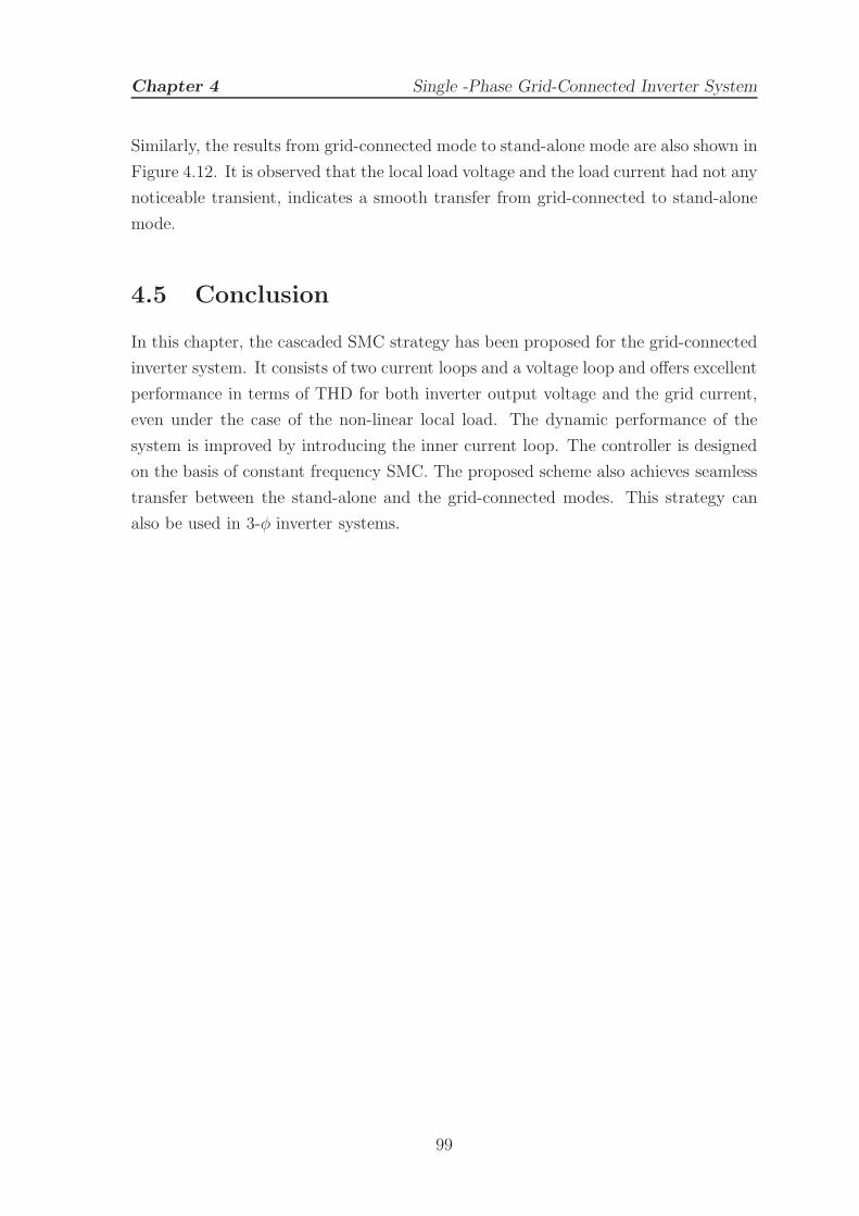
Chapter 4 Single -Phase Grid-Connected Inverter System
Similarly, the results from grid-connected mode to stand-alone mode are also shown in
Figure 4.12. It is observed that the local load voltage and the load current had not any
noticeable transient, indicates a smooth transfer from grid-connected to stand-alone
mode.
4.5 Conclusion
In this chapter, the cascaded SMC strategy has been proposed for the grid-connected
inverter system. It consists of two current loops and a voltage loop and offers excellent
performance in terms of THD for both inverter output voltage and the grid current,
even under the case of the non-linear local load. The dynamic performance of the
system is improved by introducing the inner current loop. The controller is designed
on the basis of constant frequency SMC. The proposed scheme also achieves seamless
transfer between the stand-alone and the grid-connected modes. This strategy can
also be used in 3-φ inverter systems.
99
Chapter 5
Dual-Stage Grid-Connected
Photovoltaic System
All the power processing stages, discussed in the previous chapters are combined here
to form a GPV system. The PV system can either be connected in Standalone mode
or in grid-connected mode. A typical stand-alone PV system comprises of a solar
array and a storage device i.e., battery. The battery is used as a backup source for
power management between the source and the load. Generally, a Lead-acid battery
is used in high power PV applications due to its low cost and availability in large size.
The modeling of a lead-acid battery by using the equivalent circuits is discussed here.
Three independent control loops are proposed to control the standalone PV system;
MPPT control loop for extracting maximum power from PV module, battery control
loop for bidirectional power flow between battery and dc-link through buck-boost
converter to keep the dc-link voltage constant and inverter control loop for maintaining
good voltage regulation and achieving fast dynamic response under sudden load
fluctuations. Similarly, a cascaded sliding mode control is proposed for GPV system
to regulate the current from PV system to the grid at a lower THD level. The stability
of the above controllers is verified by using Bode-diagram.
5.1 1-φ Standalone PV System
The standalone PV system is commonly used in remote areas where the grid is
not reachable or is not economical to install. This system can also be suitable
for telecommunications units, rural electricity supply, and auxiliary power units for
emergency services or military applications. As the solar energy is only possible during
100
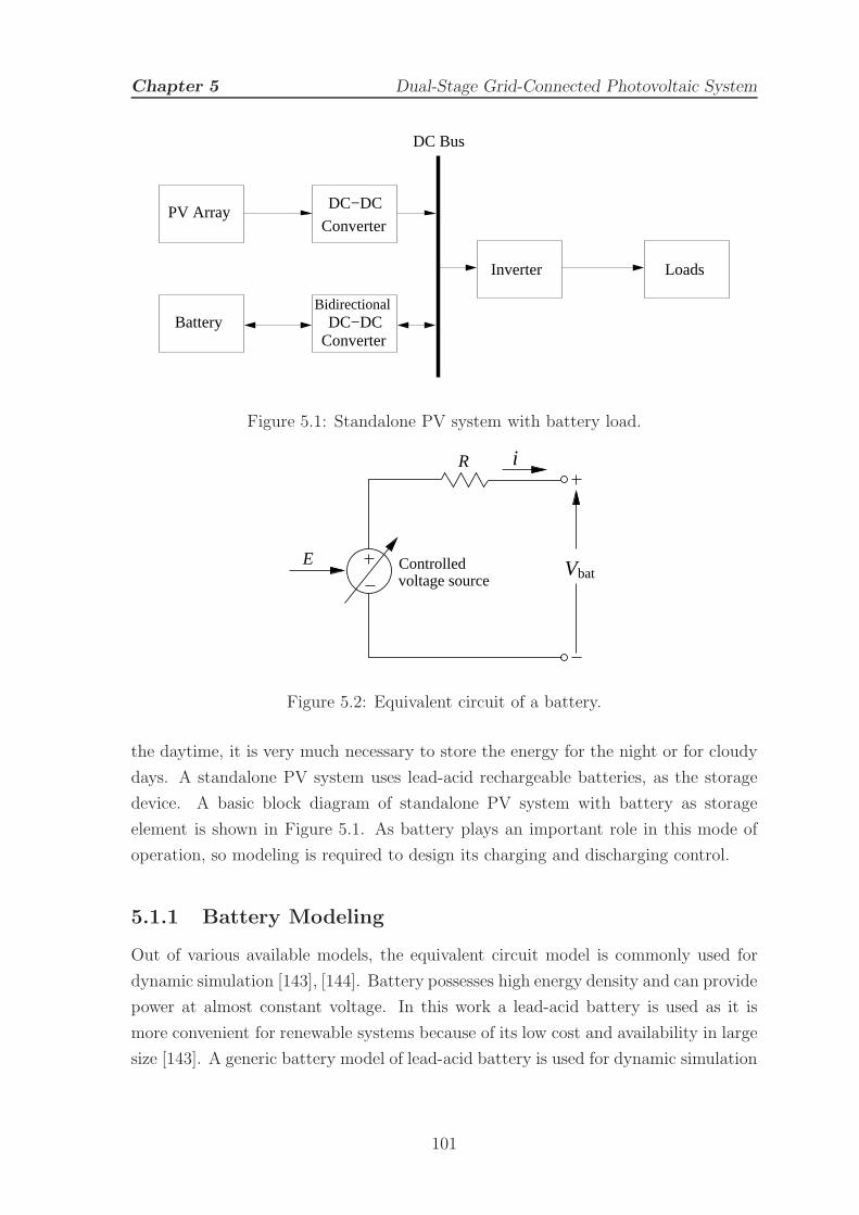
Chapter 5 Dual-Stage Grid-Connected Photovoltaic System
Inverter
PV Array
Converter
BidirectionalBattery
DC−DC
Converter
DC−DC
DC Bus
Loads
Figure 5.1: Standalone PV system with battery load.
E
R i
voltage sourceControlled Vbat
Figure 5.2: Equivalent circuit of a battery.
the daytime, it is very much necessary to store the energy for the night or for cloudy
days. A standalone PV system uses lead-acid rechargeable batteries, as the storage
device. A basic block diagram of standalone PV system with battery as storage
element is shown in Figure 5.1. As battery plays an important role in this mode of
operation, so modeling is required to design its charging and discharging control.
5.1.1 Battery Modeling
Out of various available models, the equivalent circuit model is commonly used for
dynamic simulation [143], [144]. Battery possesses high energy density and can provide
power at almost constant voltage. In this work a lead-acid battery is used as it is
more convenient for renewable systems because of its low cost and availability in large
size [143]. A generic battery model of lead-acid battery is used for dynamic simulation
101
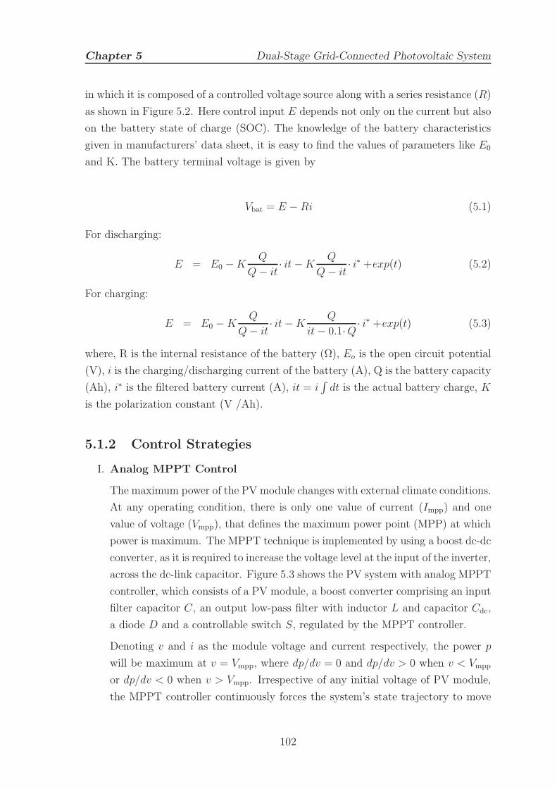
Chapter 5 Dual-Stage Grid-Connected Photovoltaic System
in which it is composed of a controlled voltage source along with a series resistance (R)
as shown in Figure 5.2. Here control input E depends not only on the current but also
on the battery state of charge (SOC). The knowledge of the battery characteristics
given in manufacturers’ data sheet, it is easy to find the values of parameters like E0
and K. The battery terminal voltage is given by
Vbat = E − Ri (5.1)
For discharging:
E = E0 −KQ
Q− it· it−K
Q
Q− it· i∗ +exp(t) (5.2)
For charging:
E = E0 −KQ
Q− it· it−K
Q
it− 0.1·Q · i∗ +exp(t) (5.3)
where, R is the internal resistance of the battery (Ω), Eo is the open circuit potential
(V), i is the charging/discharging current of the battery (A), Q is the battery capacity
(Ah), i∗ is the filtered battery current (A), it = i∫dt is the actual battery charge, K
is the polarization constant (V /Ah).
5.1.2 Control Strategies
I. Analog MPPT Control
The maximum power of the PV module changes with external climate conditions.
At any operating condition, there is only one value of current (Impp) and one
value of voltage (Vmpp), that defines the maximum power point (MPP) at which
power is maximum. The MPPT technique is implemented by using a boost dc-dc
converter, as it is required to increase the voltage level at the input of the inverter,
across the dc-link capacitor. Figure 5.3 shows the PV system with analog MPPT
controller, which consists of a PV module, a boost converter comprising an input
filter capacitor C, an output low-pass filter with inductor L and capacitor Cdc,
a diode D and a controllable switch S, regulated by the MPPT controller.
Denoting v and i as the module voltage and current respectively, the power p
will be maximum at v = Vmpp, where dp/dv = 0 and dp/dv > 0 when v < Vmpp
or dp/dv < 0 when v > Vmpp. Irrespective of any initial voltage of PV module,
the MPPT controller continuously forces the system’s state trajectory to move
102
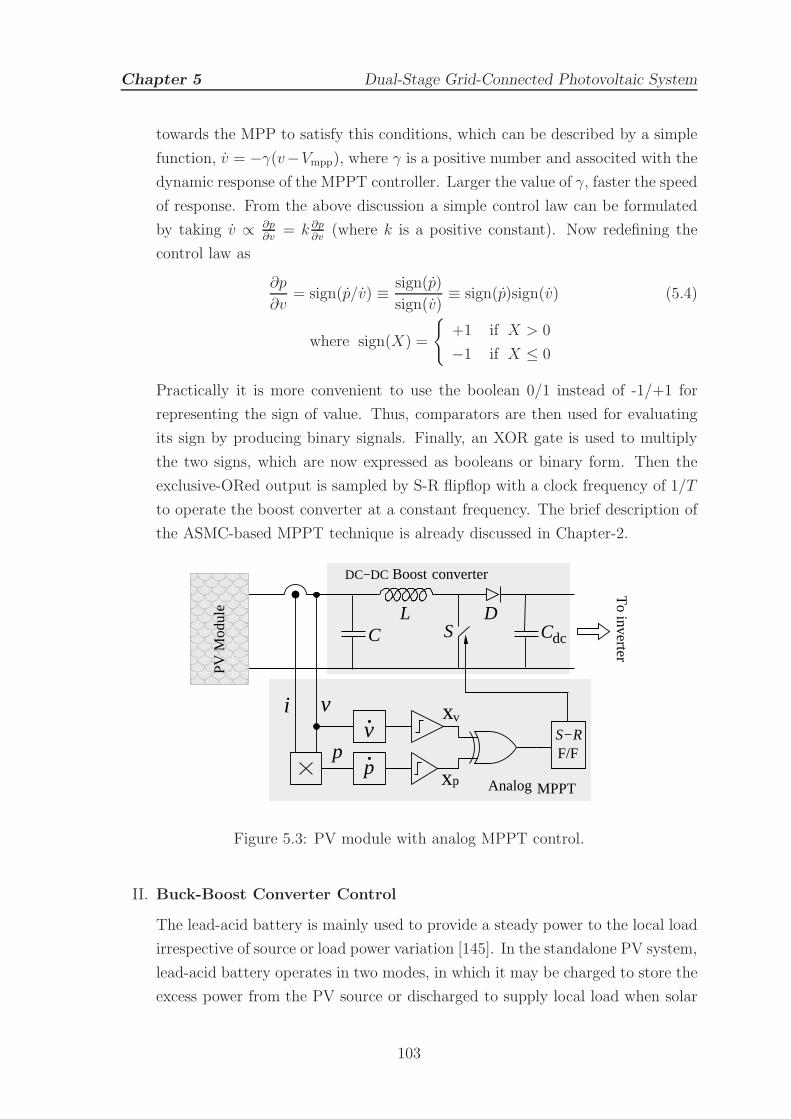
Chapter 5 Dual-Stage Grid-Connected Photovoltaic System
towards the MPP to satisfy this conditions, which can be described by a simple
function, v = −γ(v−Vmpp), where γ is a positive number and associted with the
dynamic response of the MPPT controller. Larger the value of γ, faster the speed
of response. From the above discussion a simple control law can be formulated
by taking v ∝ ∂p∂v
= k ∂p∂v
(where k is a positive constant). Now redefining the
control law as
∂p
∂v= sign(p/v) ≡ sign(p)
sign(v)≡ sign(p)sign(v) (5.4)
where sign(X) =
+1 if X > 0
−1 if X ≤ 0
Practically it is more convenient to use the boolean 0/1 instead of -1/+1 for
representing the sign of value. Thus, comparators are then used for evaluating
its sign by producing binary signals. Finally, an XOR gate is used to multiply
the two signs, which are now expressed as booleans or binary form. Then the
exclusive-ORed output is sampled by S-R flipflop with a clock frequency of 1/T
to operate the boost converter at a constant frequency. The brief description of
the ASMC-based MPPT technique is already discussed in Chapter-2.
C
xvi v
vp
xp
F/F
DC−DC Boost converter
inverterT
o
MPPT
PV
Mod
ule
S−R
p
dc
LC
DS
Analog
Figure 5.3: PV module with analog MPPT control.
II. Buck-Boost Converter Control
The lead-acid battery is mainly used to provide a steady power to the local load
irrespective of source or load power variation [145]. In the standalone PV system,
lead-acid battery operates in two modes, in which it may be charged to store the
excess power from the PV source or discharged to supply local load when solar
103
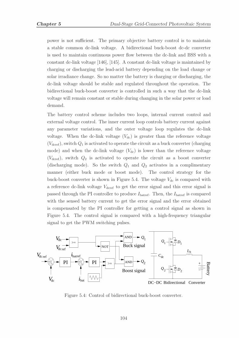
Chapter 5 Dual-Stage Grid-Connected Photovoltaic System
power is not sufficient. The primary objective battery control is to maintain
a stable common dc-link voltage. A bidirectional buck-boost dc-dc converter
is used to maintain continuous power flow between the dc-link and BSS with a
constant dc-link voltage [146], [145]. A constant dc-link voltage is maintained by
charging or discharging the lead-acid battery depending on the load change or
solar irradiance change. So no matter the battery is charging or discharging, the
dc-link voltage should be stable and regulated throughout the operation. The
bidirectional buck-boost converter is controlled in such a way that the dc-link
voltage will remain constant or stable during changing in the solar power or load
demand.
The battery control scheme includes two loops, internal current control and
external voltage control. The inner current loop controls battery current against
any parameter variations, and the outer voltage loop regulates the dc-link
voltage. When the dc-link voltage (Vdc) is greater than the reference voltage
(Vdcref), switch Q1 is activated to operate the circuit as a buck converter (charging
mode) and when the dc-link voltage (Vdc) is lower than the reference voltage
(Vdcref), switch Q2 is activated to operate the circuit as a boost converter
(discharging mode). So the switch Q1 and Q2 activates in a complimentary
manner (either buck mode or boost mode). The control strategy for the
buck-boost converter is shown in Figure 5.4. The voltage Vdc is compared with
a reference dc-link voltage Vdcref to get the error signal and this error signal is
passed through the PI controller to produce Ibatref . Then, the Ibatref is compared
with the sensed battery current to get the error signal and the error obtained
is compensated by the PI controller for getting a control signal as shown in
Figure 5.4. The control signal is compared with a high-frequency triangular
signal to get the PWM switching pulses.
1Q
2Q
+−
+− >=
D1
D2
Cdc
DC−DC Bidirectional Converter
LbV
AND
>=
i
V
V
V i
dc
dcref
dcref
dc bat
batref
AND
NOT Buck signal
Boost signal
Battery
PIPI
Q
Q
1
2 +
−
Figure 5.4: Control of bidirectional buck-boost converter.
104
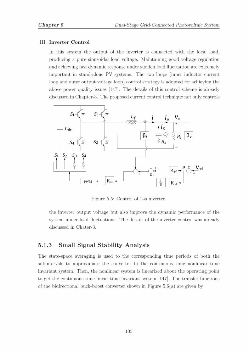
Chapter 5 Dual-Stage Grid-Connected Photovoltaic System
III. Inverter Control
In this system the output of the inverter is connected with the local load,
producing a pure sinusoidal load voltage. Maintaining good voltage regulation
and achieving fast dynamic response under sudden load fluctuation are extremely
important in stand-alone PV systems. The two loops (inner inductor current
loop and outer output voltage loop) control strategy is adopted for achieving the
above power quality issues [147]. The details of this control scheme is already
discussed in Chapter-3. The proposed current control technique not only controls
vβ
i 03S1S
2S4S
21S 3 S4S S
0vi cCf
1S
+
+
i3Κ
p3Κ
i4Κ
e
PWM
+
β iCdc
fL
L
i
RdR
+
vref
+
Figure 5.5: Control of 1-φ inverter.
the inverter output voltage but also improve the dynamic performance of the
system under load fluctuations. The details of the inverter control was already
discussed in Chater-3.
5.1.3 Small Signal Stability Analysis
The state-space averaging is used to the corresponding time periods of both the
subintervals to approximate the converter to the continuous time nonlinear time
invariant system. Then, the nonlinear system is linearized about the operating point
to get the continuous time linear time invariant system [147]. The transfer functions
of the bidirectional buck-boost converter shown in Figure 5.6(a) are given by
105

Chapter 5 Dual-Stage Grid-Connected Photovoltaic System
+−
β i βv
1(s) Gi1(s)d dcVVdc
i+
−Gid(s)
l
Vdc ref
Fm1Gv
L iV1
L 1
(a)
−++
−
βvLL
d(s)2i Fm2 GGGv2
(s)0V
i1fd1(s)
βi
refVilV0
vi
22
il
(b)
f
f
Figure 5.6: Control block diagram: (a) bidirectional buck-boost converter; (b)
inverter.
il(s)
d(s)=
VdcZdcCdcs + Vdc +D′Zdcil
LCdcZdcs2 + Ls +D′2Zdc
(5.5)
Vdc(s)
il(s)=
ZdcVdcD′ − LZdcils
VdcZdcCdcs + Vdc +D′Zdcil(5.6)
Let Gild(s) =il(s)
d(s)and transfer functions of the current loop and voltage loop controller
are Gi1(s) = Kp1 +Ki1
sand Gv1(s) = Kp2 +
Ki2
srespectively.
The control block diagram shown in Figure 5.6(a), Fm1= 1 is the gain of PWM
and βv = 0.06, βi = 0.02 are the voltage and current sensor gains respectively. Using
all the transfer functions, the current loop (Li1) gain and voltage loop (Lv1) gain of
the bidirectional buck-boost control system can be found. The stability of both the
control loops for the controller tunning parameters are verified by plotting the Bode
diagram for current loop and voltage loop. The inner current loop, Li1 has infinite gain
margin and phase margin of 89.9 deg (see Figure 5.7(a)). Similarly the outer voltage
loop, Lv1 has gain margin of 50.3 dB and phase margin of 82.8 deg (see Figure 5.7(b)).
Similarly, the transfer functions for the single phase VSI shown in Figure 5.6(b)
are given by
106
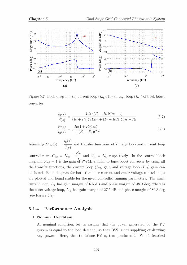
Chapter 5 Dual-Stage Grid-Connected Photovoltaic System
10 10 10 10 10−1−2 0 1 210
3
0
90
0
20
40
Frequency (Hz)
−90
Mag
nitu
de (
dB)
Pha
se (
deg)
(a)
(a)
10
Frequency (Hz)
100
Mag
nitu
de (
dB)
10 1010−2 0 2 4
0
50
−50
−100
0
90
−90Pha
se (
deg)
(b)
(b)
Figure 5.7: Bode diagram: (a) current loop (Li1); (b) voltage loop (Lv1) of buck-boost
converter.
ilf(s)
d(s)=
2Vdc((Rl + Rd)Cfs+ 1)
(Rl +Rd)CfLfs2 + (Lf +RlRdCf)s+Rl(5.7)
v0(s)
ilf(s)=
Rl(1 +RdCfs)
1 + (Rl +Rd)Cfs(5.8)
Assuming Gilfd(s) =ilf(s)
d(s)and transfer functions of voltage loop and current loop
controller are Gv2 = Kp3 +Ki3
sand Gi2 = Ki4 respectively. In the control block
diagram, Fm2 = 1 is the gain of PWM. Similar to buck-boost converter by using all
the transfer functions, the current loop (Li2) gain and voltage loop (Lv2) gain can
be found. Bode diagram for both the inner current and outer voltage control loops
are plotted and found stable for the given controller tunning parameters. The inner
current loop, Li2 has gain margin of 6.5 dB and phase margin of 48.9 deg, whereas
the outer voltage loop, Lv2 has gain margin of 27.5 dB and phase margin of 80.8 deg
(see Figure 5.8).
5.1.4 Performance Analysis
I. Nominal Condition
At nominal condition, let us assume that the power generated by the PV
system is equal to the load demand, so that BSS is not supplying or drawing
any power. Here, the standalone PV system produces 2 kW of electrical
107

Chapter 5 Dual-Stage Grid-Connected Photovoltaic System
10
0
−1 101
103
Frequency (Hz)
40
20
0
Mag
nitu
de (
dB)
Pha
se (
deg)
−20
−40
−90
90
105
(a)
0
100
50
−100
Mag
nitu
de (
dB)
−50
0
−90
90
Pha
se (
deg)
101
10−1
103
105
Frequency (Hz)
(b)
Figure 5.8: Bode diagram: (a) current loop (Li2); (b) voltage loop (Lv2) of inverter.
Table 5.1: Key Parameters for stand-alone mode
Boost, Buck-Boost, Inverter Controller and PV parameters
L = 3 mH, C = 0.2 mF Kp1= 0.1, Ki1 = 0.05, Kp2= 0.08
Lf = 1.7 mH, Cf = 66 µF Ki2 = 512, Kp3= 4.2, Ki3= 100
Cdc = 2000 µF, Lb = 2 mH Ki4=3.8, Isc = 3.8 A, Voc = 21.1 V
Vdc= 250 V, v0= 110 V(rms) Vmpp = 17.1 V, and Impp = 3.5 A
power at nominal condition and its steady state output voltage (v0) and load
current (i0) are shown in Figure 5.9(a) and (b) respectively. The steady
state dc-link voltage and its reference voltage is shown in Figure 5.10(a).
Its proper tracking shows the effectiveness of the battery controller by
using bidirectional dc-dc converter. As BSS is not charging or discharging
during this time, so its SOC curve remains constant as shown in Figure 5.10(b).
II. Load Variation
When load varies, there will be a power mismatch between PV generation and
local load, and that power gap can be fulfilled by using the BSS. The Load power
demand is varied from 1.6 kW to 2 kW to 2.4 kW. For this load variation, the
108
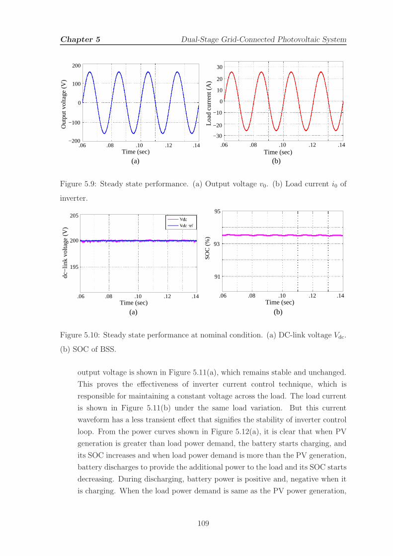
Chapter 5 Dual-Stage Grid-Connected Photovoltaic System
(a)Time (sec)
.06 .08 .10 .12 .14
200
100
0
−100
−200
Out
put v
olta
ge (
V)
Load
cur
rent
(A
)
(b)
.06 .08 .10 .12 .14Time (sec)
10
0
−10
−20
−30
30
20
Figure 5.9: Steady state performance. (a) Output voltage v0. (b) Load current i0 of
inverter.
dc−
link
volta
ge (
V)
205
200
195
.06 .08 .10 .12 .14Time (sec)
(a)
.08.06 .10 .12 .14Time (sec)
(b)
95
93
91
SO
C (
%)
Figure 5.10: Steady state performance at nominal condition. (a) DC-link voltage Vdc.
(b) SOC of BSS.
output voltage is shown in Figure 5.11(a), which remains stable and unchanged.
This proves the effectiveness of inverter current control technique, which is
responsible for maintaining a constant voltage across the load. The load current
is shown in Figure 5.11(b) under the same load variation. But this current
waveform has a less transient effect that signifies the stability of inverter control
loop. From the power curves shown in Figure 5.12(a), it is clear that when PV
generation is greater than load power demand, the battery starts charging, and
its SOC increases and when load power demand is more than the PV generation,
battery discharges to provide the additional power to the load and its SOC starts
decreasing. During discharging, battery power is positive and, negative when it
is charging. When the load power demand is same as the PV power generation,
109

Chapter 5 Dual-Stage Grid-Connected Photovoltaic System
.06 .08 .10 .12 .14Time (sec)
(a)
100
0
−100
−200
200O
utpu
t vol
tage
(V
)
20
10
30
0
Load
cur
rent
(A
)
−10
−20
−30
.06 .08 .10 .12 .14
(b)Time (sec)
Figure 5.11: Transient performance under load variation. (a) Output voltage v0. (b)
Load current i0.
battery need not to take or supply any power, which keeps its SOC remains
constant, shown in Figure 5.12(b).
(a)
.06 .10 .14 .18 .22Time (sec)
Pow
er (
W)
2500
2000
1500
1000
500
0
−500.22.18.14.10.06
Time (sec)
(b)
95
100
90
SO
C (
%)
Figure 5.12: Transient performance under load variation. (a) DC-link voltage Vdc.
(b) SOC of BSS.
III. Variation of Solar Irradiance
When PV generation power is not sufficient to supply the load demand, BSS
needs to provide the extra power through the discharging process and this
condition is called underproduction. When PV generation power is more than
the load power demand, the BSS needs to store the excess power through the
charging process, and this condition is called overproduction. Solar generated
power is varied by varying its irradiance level from 800 W/m2 to 1000 W/m2
to 1200 W/m2. Figure 5.13(a) and (b) show the output voltage and load
110
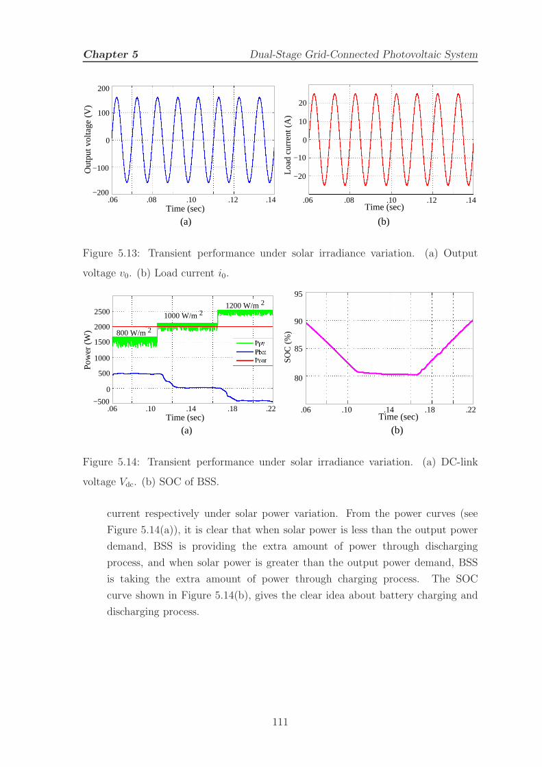
Chapter 5 Dual-Stage Grid-Connected Photovoltaic System
(a)
.06 .08 .10 .12 .14
200
100
0
−100
−200
Out
put v
olta
ge (
V)
Time (sec) Time (sec)
(b)
.06 .08 .10 .12 .14
20
10
0
−20
−10
Load
cur
rent
(A
)
Figure 5.13: Transient performance under solar irradiance variation. (a) Output
voltage v0. (b) Load current i0.
1000 W/m2
800 W/m2
1200 W/m2
.06 .10 .14 .18 .22Time (sec)
(a)
−500
0
500
1000
1500
2000
2500
Pow
er (
W)
Time (sec).22.18.14.10.06
(b)
95
90
85
80
SO
C (
%)
Figure 5.14: Transient performance under solar irradiance variation. (a) DC-link
voltage Vdc. (b) SOC of BSS.
current respectively under solar power variation. From the power curves (see
Figure 5.14(a)), it is clear that when solar power is less than the output power
demand, BSS is providing the extra amount of power through discharging
process, and when solar power is greater than the output power demand, BSS
is taking the extra amount of power through charging process. The SOC
curve shown in Figure 5.14(b), gives the clear idea about battery charging and
discharging process.
111
Chapter 5 Dual-Stage Grid-Connected Photovoltaic System
5.2 1-φ Grid-Connected PV System
5.2.1 Two-stage Architecture
In this work, a GPV system with peak power capacity of 2 kW is interfaced with
the utility grid through the LCL filter. A two-stage topology is introduced for
interfacing the PV system and the distribution network. The first stage consists
of a non-isolated dc-dc boost converter. This converter is employed to achieve high
efficiency and track the maximum power point of each PV panel. The dc-dc boost
converter operates in continuous conduction mode (CCM) along its overall operational
range. A single-phase full bridge two-level voltage source inverter is the second stage,
which is used for transferring power from PV system to the grid. The dc-link capacitor
Cdc is used to keep the input voltage of the inverter constant. The dc-link voltage
is regulated with a level higher than the peak voltage of the grid in order to ensure
the adequate direction of the power flow. The inverter is interfacing with the grid by
an inductor L2, whereas the high-frequency switching harmonics are suppressed by
the LC filter of inductance L1, and capacitance C. The GPV system parameters are
given in Table 5.2.
5.2.2 System Control Description
The schematic control diagram for two-stage single-phase GPV system is shown
in Figure 5.15. The main objective of this controller is to improve the dynamic
performance of the inverter as well as to achieve low THD grid current i2. The
proposed controller consists of three loops; an outer dc voltage control loop to regulate
the dc-link voltage Vdc, the grid current loop to control the grid current ig so that it
exactly in phase with the grid voltage, and also used for grid synchronization, and
an inner current control loop to improve the dynamic performance of the inverter by
sensing the inverter side inductor current i1. Here the voltage (VPV) and the power
(PPV) are continuously sensed to calculate the instantaneous power. The MPPT
algorithm is based on the sliding mode control to track the maximum PV power. In
order to keep power balanced between the PV system and the grid, a dc-link voltage
controller is used to keep the voltage constant. The dc-link voltage can be controlled
by controlling the current injected into the grid. Suppose the irradiation is increasing,
the dc link voltage increases, as the dc-dc converter stage is operating with MPPT.
When Vdc is greater than V ∗
dc, the dc-link voltage controller output, Id increases so
112
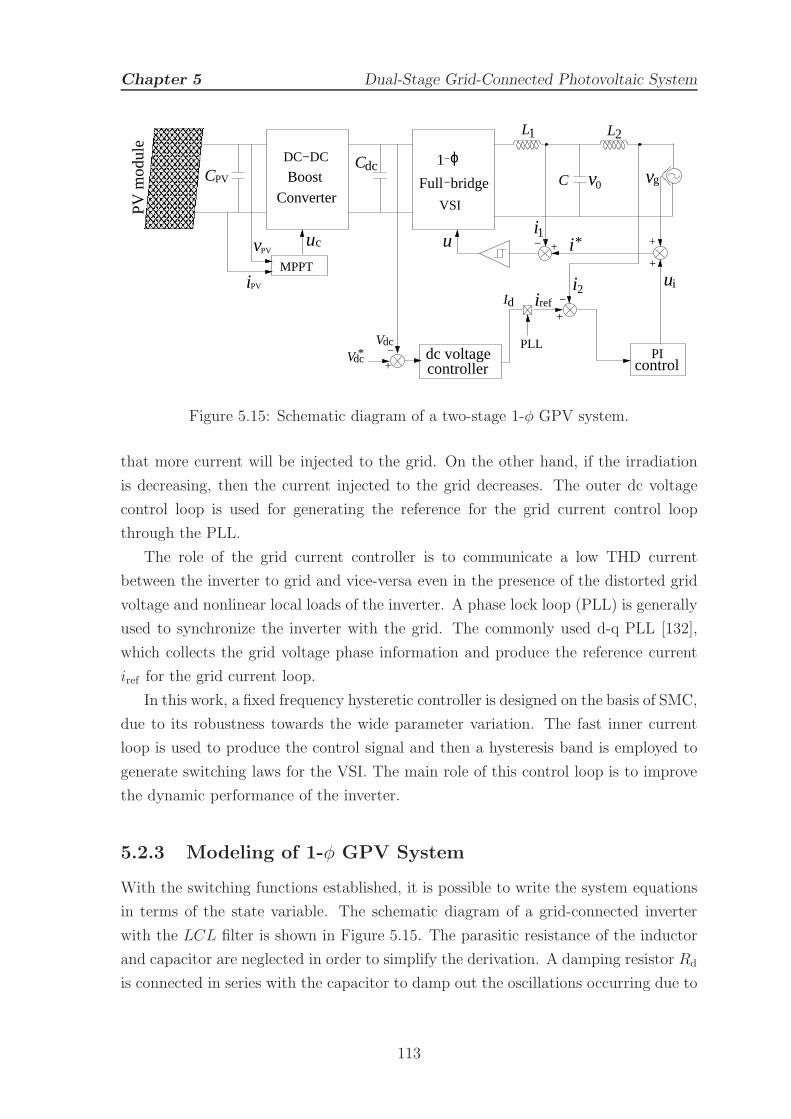
Chapter 5 Dual-Stage Grid-Connected Photovoltaic System
−
CPVC
dc
−
dc*−
DC−DC
Boost
VSI
−
V
uc
Converter
ui
ii
v0C
2iref
*1u
L1 L2
i
PV
PV
−
PV
mod
ule
d
1 ϕ
+
+
+
+
+
MPPT
PLL
I
dc
v
V
vg
i
Full bridge
dc voltagecontroller
PIcontrol
Figure 5.15: Schematic diagram of a two-stage 1-φ GPV system.
that more current will be injected to the grid. On the other hand, if the irradiation
is decreasing, then the current injected to the grid decreases. The outer dc voltage
control loop is used for generating the reference for the grid current control loop
through the PLL.
The role of the grid current controller is to communicate a low THD current
between the inverter to grid and vice-versa even in the presence of the distorted grid
voltage and nonlinear local loads of the inverter. A phase lock loop (PLL) is generally
used to synchronize the inverter with the grid. The commonly used d-q PLL [132],
which collects the grid voltage phase information and produce the reference current
iref for the grid current loop.
In this work, a fixed frequency hysteretic controller is designed on the basis of SMC,
due to its robustness towards the wide parameter variation. The fast inner current
loop is used to produce the control signal and then a hysteresis band is employed to
generate switching laws for the VSI. The main role of this control loop is to improve
the dynamic performance of the inverter.
5.2.3 Modeling of 1-φ GPV System
With the switching functions established, it is possible to write the system equations
in terms of the state variable. The schematic diagram of a grid-connected inverter
with the LCL filter is shown in Figure 5.15. The parasitic resistance of the inductor
and capacitor are neglected in order to simplify the derivation. A damping resistor Rd
is connected in series with the capacitor to damp out the oscillations occurring due to
113
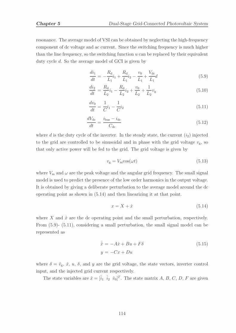
Chapter 5 Dual-Stage Grid-Connected Photovoltaic System
resonance. The average model of VSI can be obtained by neglecting the high-frequency
component of dc voltage and ac current. Since the switching frequency is much higher
than the line frequency, so the switching function u can be replaced by their equivalent
duty cycle d. So the average model of GCI is given by
di1
dt= −
Rd
L1
i1 +Rd
L1
i2 −v0
L1
+Vdc
L1
d (5.9)
di2dt
=Rd
L2i1 −
Rd
L2i2 +
v0L2
+1
L2vg (5.10)
dv0
dt=
1
Ci1 −
1
Ci2 (5.11)
dVdc
dt=
ibus − idc
Cdc
(5.12)
where d is the duty cycle of the inverter. In the steady state, the current (i2) injected
to the grid are controlled to be sinusoidal and in phase with the grid voltage vg, so
that only active power will be fed to the grid. The grid voltage is given by
vg = Vmcos(ωt) (5.13)
where Vm and ω are the peak voltage and the angular grid frequency. The small signal
model is used to predict the presence of the low order harmonics in the output voltage.
It is obtained by giving a deliberate perturbation to the average model around the dc
operating point as shown in (5.14) and then linearizing it at that point.
x = X + x (5.14)
where X and x are the dc operating point and the small perturbation, respectively.
From (5.9)- (5.11), considering a small perturbation, the small signal model can be
represented as
˙x = −Ax+Bu+ Fδ (5.15)
y = −Cx+Du
where δ = vg, x, u, δ, and y are the grid voltage, the state vectors, inverter control
input, and the injected grid current respectively.
The state variables are x = [i1 i2 v0]T . The state matrix A, B, C, D, F are given
114
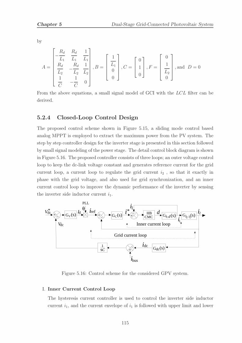
Chapter 5 Dual-Stage Grid-Connected Photovoltaic System
by
A =
−Rd
L1
Rd
L1
1
L1
Rd
L2−Rd
L2
1
L2
1
C−
1
C0
, B =
1
L1
0
0
, C =
0
1
0
, F =
0
1
L2
0
, and D = 0
From the above equations, a small signal model of GCI with the LCL filter can be
derived.
5.2.4 Closed-Loop Control Design
The proposed control scheme shown in Figure 5.15, a sliding mode control based
analog MPPT is employed to extract the maximum power from the PV system. The
step by step controller design for the inverter stage is presented in this section followed
by small signal modeling of the power stage. The detail control block diagram is shown
in Figure 5.16. The proposed controller consists of three loops; an outer voltage control
loop to keep the dc-link voltage constant and generates reference current for the grid
current loop, a current loop to regulate the grid current i2 , so that it exactly in
phase with the grid voltage, and also used for grid synchronization, and an inner
current control loop to improve the dynamic performance of the inverter by sensing
the inverter side inductor current i1.
+− +
−
−+
(s)dcG
Vdc
dc*V Id refi i*
i1i2
G (s) (s)
−+
idc
ibus
Inner current loop
Grid current loop
i1d
PLL
(s)G(s)θ
Cs1
G di1 i2 i1CG HBCMCV
Figure 5.16: Control scheme for the considered GPV system.
I. Inner Current Control Loop
The hysteresis current controller is used to control the inverter side inductor
current i1, and the current envelope of i1 is followed with upper limit and lower
115
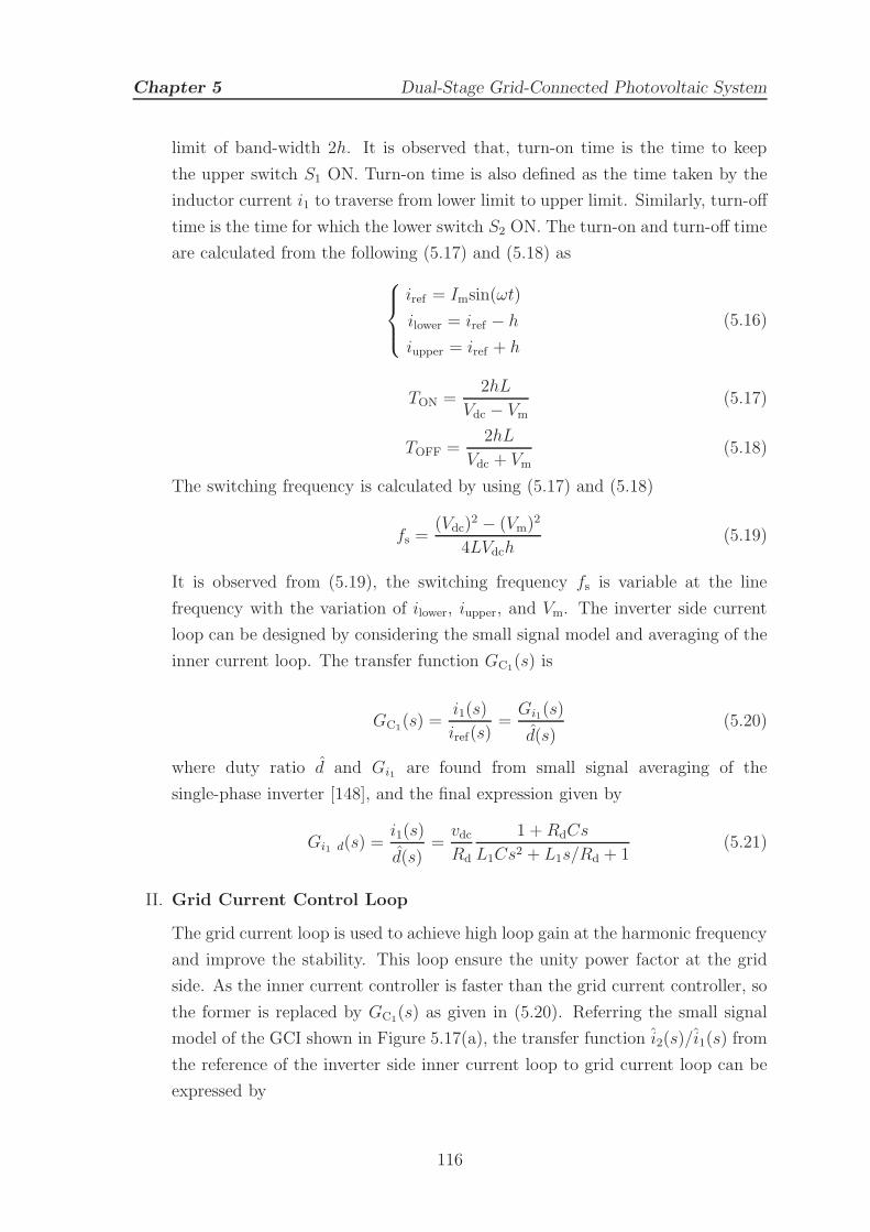
Chapter 5 Dual-Stage Grid-Connected Photovoltaic System
limit of band-width 2h. It is observed that, turn-on time is the time to keep
the upper switch S1 ON. Turn-on time is also defined as the time taken by the
inductor current i1 to traverse from lower limit to upper limit. Similarly, turn-off
time is the time for which the lower switch S2 ON. The turn-on and turn-off time
are calculated from the following (5.17) and (5.18) as
iref = Imsin(ωt)
ilower = iref − h
iupper = iref + h
(5.16)
TON =2hL
Vdc − Vm(5.17)
TOFF =2hL
Vdc + Vm(5.18)
The switching frequency is calculated by using (5.17) and (5.18)
fs =(Vdc)
2 − (Vm)2
4LVdch(5.19)
It is observed from (5.19), the switching frequency fs is variable at the line
frequency with the variation of ilower, iupper, and Vm. The inverter side current
loop can be designed by considering the small signal model and averaging of the
inner current loop. The transfer function GC1(s) is
GC1(s) =
i1(s)
iref(s)=
Gi1(s)
d(s)(5.20)
where duty ratio d and Gi1 are found from small signal averaging of the
single-phase inverter [148], and the final expression given by
Gi1 d(s) =i1(s)
d(s)=
vdcRd
1 +RdCs
L1Cs2 + L1s/Rd + 1(5.21)
II. Grid Current Control Loop
The grid current loop is used to achieve high loop gain at the harmonic frequency
and improve the stability. This loop ensure the unity power factor at the grid
side. As the inner current controller is faster than the grid current controller, so
the former is replaced by GC1(s) as given in (5.20). Referring the small signal
model of the GCI shown in Figure 5.17(a), the transfer function i2(s)/i1(s) from
the reference of the inverter side inner current loop to grid current loop can be
expressed by
116
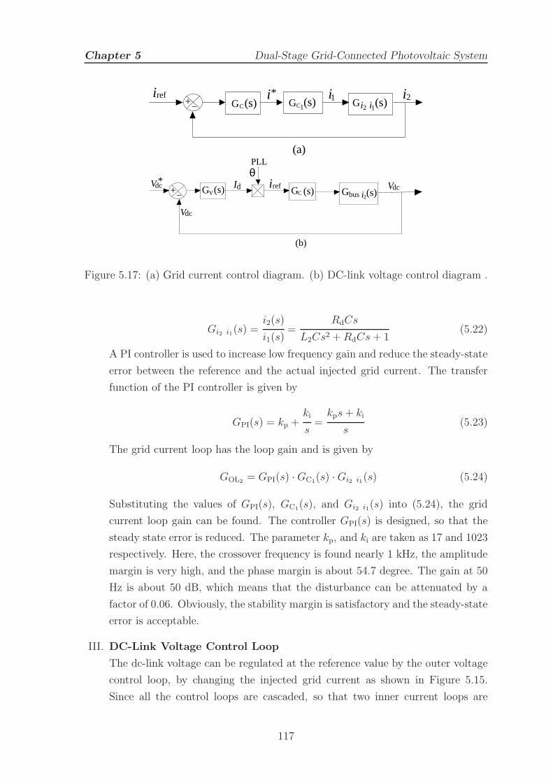
Chapter 5 Dual-Stage Grid-Connected Photovoltaic System
+−
* i(s)
i 1refiC(s) C1GG Gi2 i1
i2(s)
(a)
+−I
θd Vdc
busi2(s)GCi ref G (s)(s)
V
Vdc
dc*
PLL
G
(b)
V
Figure 5.17: (a) Grid current control diagram. (b) DC-link voltage control diagram .
Gi2 i1(s) =i2(s)
i1(s)=
RdCs
L2Cs2 +RdCs+ 1(5.22)
A PI controller is used to increase low frequency gain and reduce the steady-state
error between the reference and the actual injected grid current. The transfer
function of the PI controller is given by
GPI(s) = kp +ki
s=
kps+ ki
s(5.23)
The grid current loop has the loop gain and is given by
GOL2= GPI(s) ·GC1
(s) ·Gi2 i1(s) (5.24)
Substituting the values of GPI(s), GC1(s), and Gi2 i1(s) into (5.24), the grid
current loop gain can be found. The controller GPI(s) is designed, so that the
steady state error is reduced. The parameter kp, and ki are taken as 17 and 1023
respectively. Here, the crossover frequency is found nearly 1 kHz, the amplitude
margin is very high, and the phase margin is about 54.7 degree. The gain at 50
Hz is about 50 dB, which means that the disturbance can be attenuated by a
factor of 0.06. Obviously, the stability margin is satisfactory and the steady-state
error is acceptable.
III. DC-Link Voltage Control Loop
The dc-link voltage can be regulated at the reference value by the outer voltage
control loop, by changing the injected grid current as shown in Figure 5.15.
Since all the control loops are cascaded, so that two inner current loops are
117
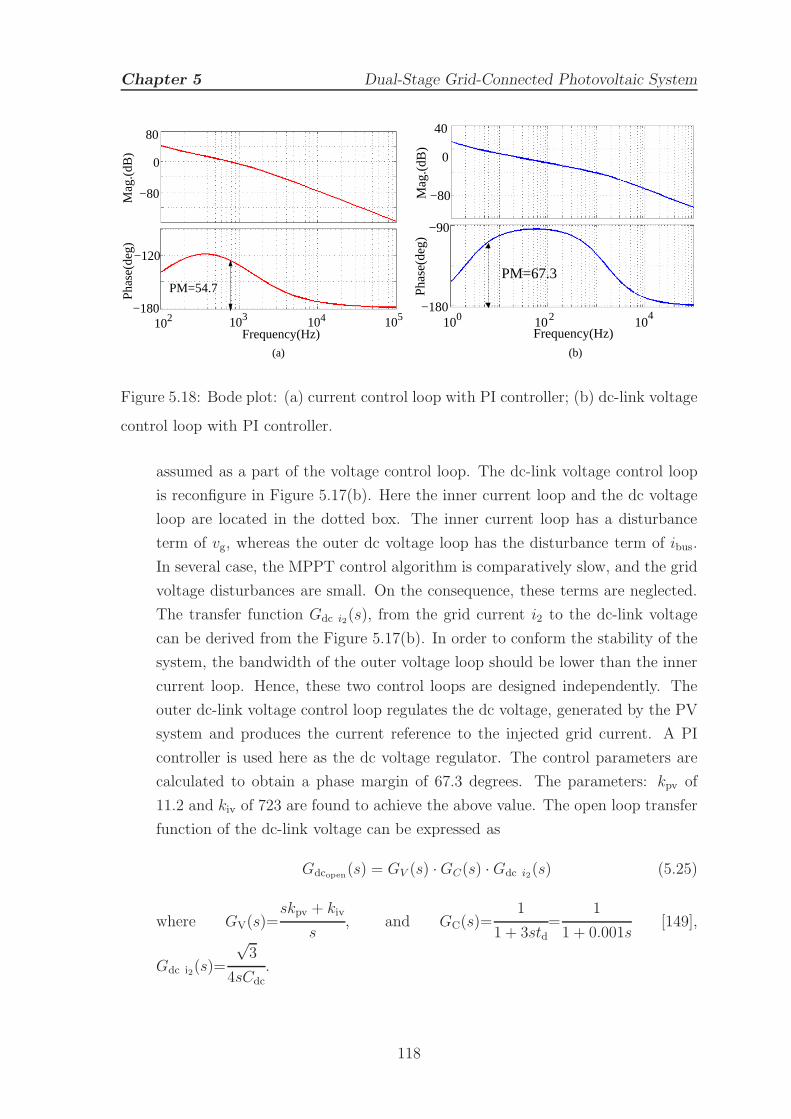
Chapter 5 Dual-Stage Grid-Connected Photovoltaic System
−80
0
80
102 103 104 105
−120
−180
Frequency(Hz)
Mag
.(dB
)P
hase
(deg
)
PM=54.7
(a)
0
10−180
Frequency(Hz)0 102 10
4
−90
Pha
se(d
eg)
Mag
.(dB
)
40
−80
PM=67.3
(b)
Figure 5.18: Bode plot: (a) current control loop with PI controller; (b) dc-link voltage
control loop with PI controller.
assumed as a part of the voltage control loop. The dc-link voltage control loop
is reconfigure in Figure 5.17(b). Here the inner current loop and the dc voltage
loop are located in the dotted box. The inner current loop has a disturbance
term of vg, whereas the outer dc voltage loop has the disturbance term of ibus.
In several case, the MPPT control algorithm is comparatively slow, and the grid
voltage disturbances are small. On the consequence, these terms are neglected.
The transfer function Gdc i2(s), from the grid current i2 to the dc-link voltage
can be derived from the Figure 5.17(b). In order to conform the stability of the
system, the bandwidth of the outer voltage loop should be lower than the inner
current loop. Hence, these two control loops are designed independently. The
outer dc-link voltage control loop regulates the dc voltage, generated by the PV
system and produces the current reference to the injected grid current. A PI
controller is used here as the dc voltage regulator. The control parameters are
calculated to obtain a phase margin of 67.3 degrees. The parameters: kpv of
11.2 and kiv of 723 are found to achieve the above value. The open loop transfer
function of the dc-link voltage can be expressed as
Gdcopen(s) = GV (s) ·GC(s) ·Gdc i2(s) (5.25)
where GV(s)=skpv + kiv
s, and GC(s)=
1
1 + 3std=
1
1 + 0.001s[149],
Gdc i2(s)=
√3
4sCdc
.
118
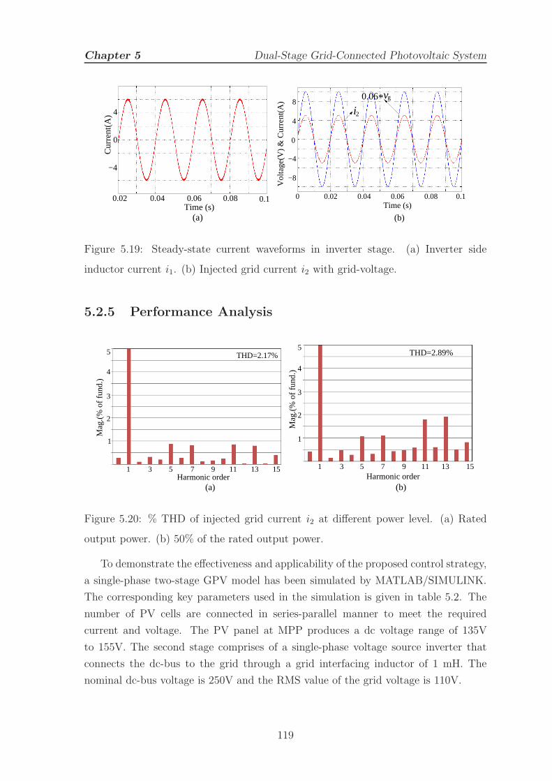
Chapter 5 Dual-Stage Grid-Connected Photovoltaic System
Cur
rent
(A)
0.10.080.040.02
4
0
−4
0.06
(a)Time (s)
2
Vol
tage
(V)
& C
urre
nt(A
) 0.06* gv
i
0 0.02
−8
−4
0
4
8
0.060.04 0.08 0.1
(b)
Time (s)
Figure 5.19: Steady-state current waveforms in inverter stage. (a) Inverter side
inductor current i1. (b) Injected grid current i2 with grid-voltage.
5.2.5 Performance Analysis
Harmonic order(a)
Mag
.(%
of f
und.
) 4
5
3
2
1
1 3 5 7 9 11 13 15
THD=2.17%
Harmonic order(b)
Mag
.(%
of f
und.
)
2
3
4
5
1
1 3 5 7 9 11 13 15
THD=2.89%
Figure 5.20: % THD of injected grid current i2 at different power level. (a) Rated
output power. (b) 50% of the rated output power.
To demonstrate the effectiveness and applicability of the proposed control strategy,
a single-phase two-stage GPV model has been simulated by MATLAB/SIMULINK.
The corresponding key parameters used in the simulation is given in table 5.2. The
number of PV cells are connected in series-parallel manner to meet the required
current and voltage. The PV panel at MPP produces a dc voltage range of 135V
to 155V. The second stage comprises of a single-phase voltage source inverter that
connects the dc-bus to the grid through a grid interfacing inductor of 1 mH. The
nominal dc-bus voltage is 250V and the RMS value of the grid voltage is 110V.
119
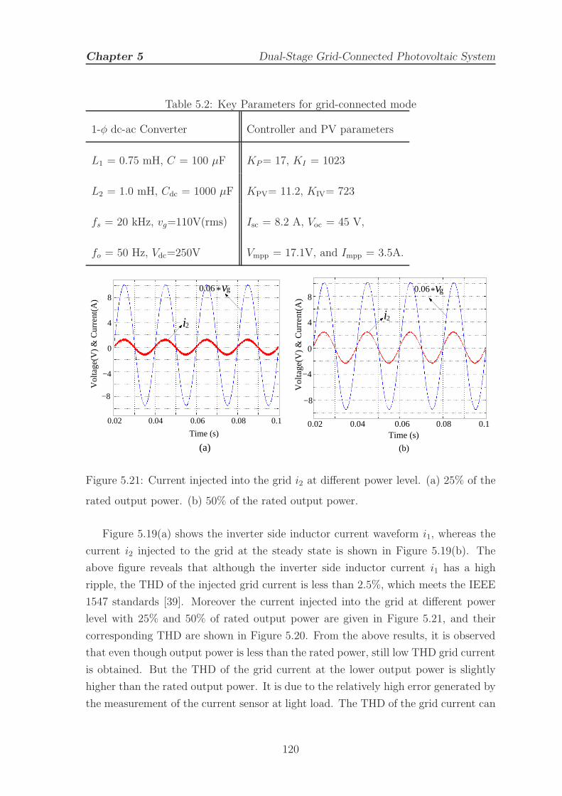
Chapter 5 Dual-Stage Grid-Connected Photovoltaic System
Table 5.2: Key Parameters for grid-connected mode
1-φ dc-ac Converter Controller and PV parameters
L1 = 0.75 mH, C = 100 µF KP= 17, KI = 1023
L2 = 1.0 mH, Cdc = 1000 µF KPV= 11.2, KIV= 723
fs = 20 kHz, vg=110V(rms) Isc = 8.2 A, Voc = 45 V,
fo = 50 Hz, Vdc=250V Vmpp = 17.1V, and Impp = 3.5A.
2
(a)
Vol
tage
(V)
& C
urre
nt(A
)
0.04 0.06 0.08 0.1
−8
−4
0
4
80.06* gv
i
0.02
Time (s)
Vol
tage
(V)
& C
urre
nt(A
)
0.02 0.04 0.06 0.08 0.1
−8
−4
0
4
8
i
(b)
gv*0.06
2
Time (s)
Figure 5.21: Current injected into the grid i2 at different power level. (a) 25% of the
rated output power. (b) 50% of the rated output power.
Figure 5.19(a) shows the inverter side inductor current waveform i1, whereas the
current i2 injected to the grid at the steady state is shown in Figure 5.19(b). The
above figure reveals that although the inverter side inductor current i1 has a high
ripple, the THD of the injected grid current is less than 2.5%, which meets the IEEE
1547 standards [39]. Moreover the current injected into the grid at different power
level with 25% and 50% of rated output power are given in Figure 5.21, and their
corresponding THD are shown in Figure 5.20. From the above results, it is observed
that even though output power is less than the rated power, still low THD grid current
is obtained. But the THD of the grid current at the lower output power is slightly
higher than the rated output power. It is due to the relatively high error generated by
the measurement of the current sensor at light load. The THD of the grid current can
120
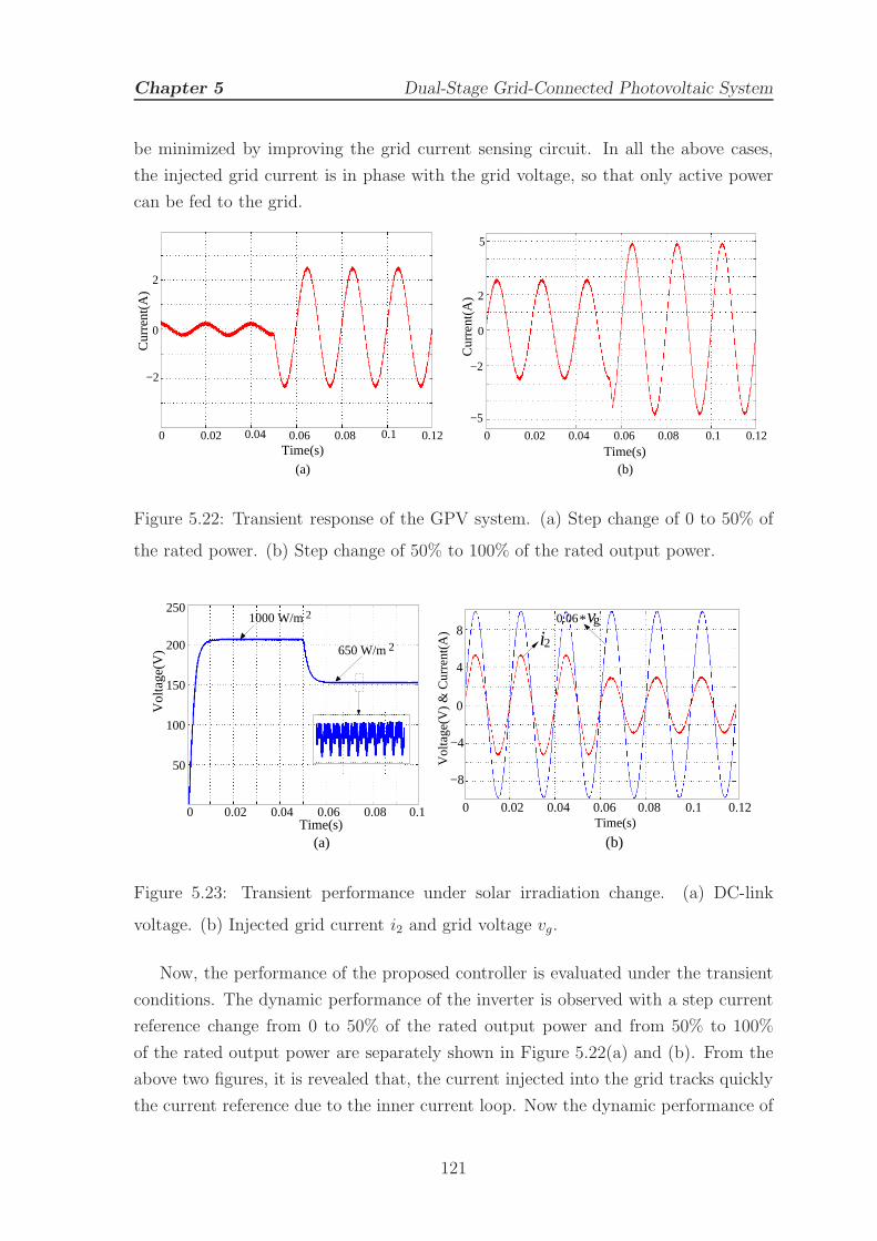
Chapter 5 Dual-Stage Grid-Connected Photovoltaic System
be minimized by improving the grid current sensing circuit. In all the above cases,
the injected grid current is in phase with the grid voltage, so that only active power
can be fed to the grid.
0 0.02 0.04 0.06 0.08 0.1 0.12
Cur
rent
(A)
2
0
−2
Time(s)
(a)
5
2
0
−2
−5
0 0.02 0.04 0.06 0.08 0.1 0.12Time(s)
(b)C
urre
nt(A
)
Figure 5.22: Transient response of the GPV system. (a) Step change of 0 to 50% of
the rated power. (b) Step change of 50% to 100% of the rated output power.
650 W/m2
1000 W/m2
0 0.02 0.04 0.06 0.08 0.1
50
100
150
200
250
Vol
tage
(V)
Time(s)(a)
4
0
−4
−8
0 0.02 0.04 0.06 0.08 0.1 0.12
Vol
tage
(V)
& C
urre
nt(A
) 8 i20.06 vg*
Time(s)
(b)
Figure 5.23: Transient performance under solar irradiation change. (a) DC-link
voltage. (b) Injected grid current i2 and grid voltage vg.
Now, the performance of the proposed controller is evaluated under the transient
conditions. The dynamic performance of the inverter is observed with a step current
reference change from 0 to 50% of the rated output power and from 50% to 100%
of the rated output power are separately shown in Figure 5.22(a) and (b). From the
above two figures, it is revealed that, the current injected into the grid tracks quickly
the current reference due to the inner current loop. Now the dynamic performance of
121
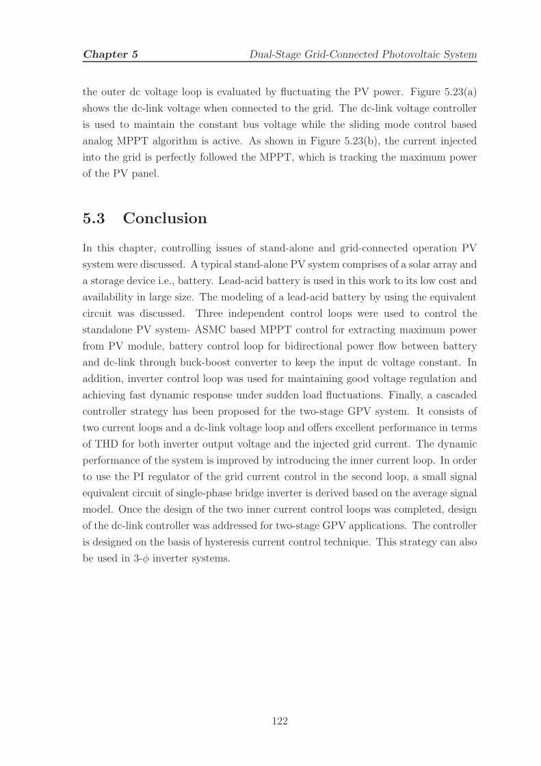
Chapter 5 Dual-Stage Grid-Connected Photovoltaic System
the outer dc voltage loop is evaluated by fluctuating the PV power. Figure 5.23(a)
shows the dc-link voltage when connected to the grid. The dc-link voltage controller
is used to maintain the constant bus voltage while the sliding mode control based
analog MPPT algorithm is active. As shown in Figure 5.23(b), the current injected
into the grid is perfectly followed the MPPT, which is tracking the maximum power
of the PV panel.
5.3 Conclusion
In this chapter, controlling issues of stand-alone and grid-connected operation PV
system were discussed. A typical stand-alone PV system comprises of a solar array and
a storage device i.e., battery. Lead-acid battery is used in this work to its low cost and
availability in large size. The modeling of a lead-acid battery by using the equivalent
circuit was discussed. Three independent control loops were used to control the
standalone PV system- ASMC based MPPT control for extracting maximum power
from PV module, battery control loop for bidirectional power flow between battery
and dc-link through buck-boost converter to keep the input dc voltage constant. In
addition, inverter control loop was used for maintaining good voltage regulation and
achieving fast dynamic response under sudden load fluctuations. Finally, a cascaded
controller strategy has been proposed for the two-stage GPV system. It consists of
two current loops and a dc-link voltage loop and offers excellent performance in terms
of THD for both inverter output voltage and the injected grid current. The dynamic
performance of the system is improved by introducing the inner current loop. In order
to use the PI regulator of the grid current control in the second loop, a small signal
equivalent circuit of single-phase bridge inverter is derived based on the average signal
model. Once the design of the two inner current control loops was completed, design
of the dc-link controller was addressed for two-stage GPV applications. The controller
is designed on the basis of hysteresis current control technique. This strategy can also
be used in 3-φ inverter systems.
122
Chapter 6
Conclusion
6.1 Summary of Contributions
PV panels convert solar energy into electric power. Voltage and current at PV
terminals have a complicated nonlinear relationship depending on the environment
temperature and irradiance. To best regulate the available power from the PV panels,
several power electronic technologies have been developed in recent decades. An
inverter achieves the dc-ac power processing stage. This inverter must guarantee that
it will inject the current into the grid at unit power factor with the lowest harmonic
distortion level. Therefore, PV inverters have an enormous impact on the performance
of PV grid-tie systems. The different GPV inverter topologies were reviewed. Among
all configuration ”string-inverter” is suitable, where each string is connected to one
inverter and inject power to the grid. Since new strings can be easily added to the
system to increase its power rating, system modularity is maximized. Due to its
extensive use and the possibility to easily add other power converter stages, this
configuration has been chosen as the power conditioning structure considered in this
work. In numerous string-inverter topologies, the dual stage inverter structure is
selected in this dissertation.
For the first dc-dc stage of the dual-stage inverters, the non-isolated converter
topologies are suitable candidates, as no transformer is required. The MPPT is used to
control dc-dc converter such that the power extracted from PV panel is maximized. An
analog circuitry based PV MPPT technique is therefore an attractive solution due to
its low cost and capability of easy integration as compared to the conventional MPPT
techniques. A fast and robust analog MPP tracker is proposed without imposing
any external control or perturbation. The fast dynamic performances with absolute
123
Chapter 6 Conclusion
robustness are ensured here by integrating the concepts of Utkin’s equivalent SMC
law and fast-scale stability analysis of actual switched converter systems. Moreover,
the superiority of the proposed MPP tracker (in terms of high tracking performances)
over classical ones, and its impact in series-connected converters configuration are
analytically demonstrated.
For the second dc-ac stage of the dual-stage inverters, the selection of the
inverter configuration, with its proper switching technique is necessary to improve
power efficiency and power density. The different inverter topologies and switching
techniques are reviewed in Chapter-3. Among them 1-φ bridge inverter with bipolar
switching technique is found to be suitable one. Moreover, a FFHC controller is
proposed to improve the good voltage regulation and the fast dynamic response under
sudden load fluctuation. The proposed controller is designed on the basis of SMC
technique. The proposed method is then applied to a 1-kVA, 110 V, 50 Hz 1-φ VSI
system. The results show that dynamic response is quite faster than that of the
widely used PWM-controlled inverter systems. Moreover, the THD of inverter output
voltage is 2.14% at standard nonlinear load IEC62040-3 as well.
In addition, a PV system can be connected to the utility grid, injecting power
into the grid besides providing power to their local loads. It is therefore important
to inject a low THD current from PV system to grid at unity power factor. This
can be achieved by using a PLL, which collects the grid voltage phase information
and produce the reference current for the Inverter. Out of the various structure, d-q
PLL is suitable for this work. In this dissertation, a cascaded SMC strategy has been
proposed for a grid-connected inverter system in order to simultaneously improve the
power quality of the local load voltage and the current exchanged with the grid. The
proposed controller also enables seamless transfer operation from stand-alone mode to
grid-connected mode and vice versa. The control scheme includes an inner voltage loop
with a proportional controller and an outer current loop with a PI-controller. This
results in a very low THD in both the grid current and the inverter local load voltage
simultaneously. The overall controller is designed on the basis of fixed-frequency
hysteresis controller. The proposed method is then applied to a 1-kVA, 110 V, 50 Hz
grid-connected 1-φ VSI system. The results show that the steady-state response and
the dynamic response are quite attractive.
All the power processing stages discussed in the previous chapters are then
combined to form a GPV system. The PV system can either be connected in
stand-alone mode or in grid-connected mode. A typical stand-alone PV system
comprises of a solar array and a storage device i.e., battery. Whereas in the GPV
system, the battery may or may not require. In the former case, a battery is used as
124
Chapter 6 Conclusion
a backup source for power management between the source and the load. Lead-acid
battery is used in high power PV applications due to its low cost and availability
in large size. The modeling of a lead-acid battery by using the equivalent circuits
are discussed here. Three independent control loops are proposed to control the
standalone PV system- MPPT control loop for extracting maximum power from PV
module, battery control loop for bidirectional power flow between battery and dc-link
through buck-boost converter to keep the input dc voltage constant. In addition,
inverter control loop is used for maintaining good voltage regulation and achieving
fast dynamic response under sudden load fluctuations. Similarly, a cascaded SMC is
proposed for GPV system to regulate the current from PV system to the grid at a
lower THD level. The stability of the above controllers are verified by using linear
stability criterion.
6.2 Future Research Directions
The further research might be focused on the following issues.
1. The proposed analog circuitry based MPPT technique was implemented for
conventional dc-dc non-isolated converters, which are operated at low duty cycle.
This MPPT could be applied for an isolated converter in quasi-resonant mode,
which can not only reduce the switching losses but also recycle the leakage
energy. Moreover, these converters have the ability to boost a lower dc voltage
level to a higher dc-link voltage.
2. For the experimental validation, the current controllers were implemented in
dSPACETM which had a time step size limit of 100 µs. A relatively smaller time
step size device such as FPGA or DSP can be utilized to achieve the control
algorithm. So that, current feedback should track the reference more quickly and
exactly, and a better performance of harmonic compensation could be expected.
This will be essential for analyzing the inner dynamics of the system.
3. The fast scale and the slow scale stability of the proposed SMC controller could
be carried out in future.
4. Less steady-state oscillations with reduced cross-coupling effects was found
for the series connected buck-type MIC. This could also be verified for the
series-connected inverter in future.
125

Bibliography
[1] Y. W. Li, D. M. Vilathgamuwa, and P. C. Loh. A grid-interfacing power quality
compansator for three-phase three-wire microgrid applications. IEEE Trans. Power Electron.,
21(4):1021–1031, July 2006.
[2] L. Philipson. Distributed and dispersed generation: addressing the spectrum of consumer
needs. In Proc. IEEE Power Engineering Society Summer Meeting, volume 3, pages 1663–1665,
2000.
[3] H. B. Puttgen, P. R. MacGregor, and F. C. Lambert. Distributed generation: Semantic hype
or the dawn of a new era? IEEE Power Energy Mag., 1(1):22–29, Jan./Feb. 2003.
[4] R. H. Lasseter. Microgrids and distributed generation. Journal of Energy Engineering,
133(3):144–149, Dec. 2007.
[5] N. Hatziargyriou, H. Asano, R. Iravani, and C. Marnay. Microgrids. IEEE Power and Energy
Mag., 5(4):78–994, Jul./Aug. 2007.
[6] F. Katiraei, R. Iravani, and N. Hatziargyriou. Microgrids management. IEEE Power and
Energy Mag., 6(3):54–65, Jun. 2008.
[7] B. Kroposki, R. H. Lasseter, T. Ise, S. Morozumi, S. Papathanassiou, and N. Hatziargyriou.
Making microgrids work. IEEE Power and Energy Mag., 6(3):41–53, May/Jun. 2008.
[8] K. Dang, J. Yu, T. Dang, and B. Han. Benefit of distributed generation on line loss reduction.
In Proc.IEEE ICECE, volume 2, pages 2042–2045, 2011.
[9] G. T. Chinery and J. M. Wood. Tva’s photovoltaic activities. IEEE Trans. Power Appl. Syst.,
104:1998–2005, Aug. 1985.
[10] T. Ackermann. Wind Power in Power Systems. J. Wiley Press, 2005.
[11] R. P. O’Hayre, S.W. Cha, W. G. Colella, and F.B. Prinz. Fuel Cell Fundamentals. John Wiley
& Sons New York, 2009.
[12] A. K. Saha, S. Chowdhury, S. P. Chowdhury, and P. A. Crossley. Modeling and performance
analysis of a microturbine as a distributed energy resource. IEEE Trans. Energy Convers.,
24(2):529–538, Mar. 2009.
126

Bibliography
[13] J. Bayamba. Photovoltaics: An energy option for sustainable development. In 3rd Wolrd Conf.
on Photovoltaic Energy Conversion, pages 174–176, 2003.
[14] J. M. Carrasco, L. G. Franquelo, J. T. Bialasiewicz, E. Galvan, R. C. P. Guisado, Ma.A.M.
Prats, J.I. Leon, and N. Moreno-Alfonso. Power-electronic systems for the grid integration of
renewable energy sources: a survey. IEEE Trans. Ind. Electron., 53(4):1002–1016, Jun. 2014.
[15] P. F. Ribeiro, B. K. Johnson, M. L. Crow, A. Asroy, and Y. Lie. Energy storage systems for
advanced power applications. In Proc.of IEEE, volume 89, pages 1744–1765, 2001.
[16] D. Cruz-Martins and R. Demonti. Photovoltaic energy processing for utility connected system.
In 27th Annual Conference of the IEEE Industrial Electronics Society, pages 1292–1296, 2011.
[17] M. Meinhardt. Past, present and future of grid-connected photovoltaic and hybrid power
systems. In Power Engineering Society Summer Meeting, volume 2, pages 1283–1288, 2010.
[18] A. Pregelj, M. Begovic, and A. Rohatgi. Impact of inverter configuration on PV system
reliability and energy production. In Twenty-Ninth IEEE Photovoltaic Specialists Conf., 2002.
[19] IEEE 519 Working Group et al. IEEE recommended practices and requirements for harmonic
control in electrical power systems. IEEE STD, pages 519–1992, 1992.
[20] T. S. Basso and R. DeBlasio. IEEE 1547 series of standards: interconnection issues. IEEE
Trans. Power Electron., 19(5):1159–1162, 2004.
[21] R. M. Swanson. A vision for crystalline silicon photovoltaics. In Progress in Photovoltaics:
Research and Applications, volume 14, pages 443–453, 2006.
[22] S. B. Kjaer, J. K. Pedersen, and F. Blaabjerg. A review of single-phase grid-connected inverters
for photovoltaic modules. IEEE Trans. Industry Applications, 41(4):1292–1306, Sep. 2015.
[23] Q. Li and P. Wolfs. A review of the single phase photovoltaic module integrated
converter topologies with three different dc link configurations. IEEE Trans. Ind. Electron.,
23(4):1320–1333, May. 2008.
[24] M. Calais, J. Myrzik, T. Spooner, and V. G. Agelidis. Inverters for single-phase grid-connected
photovoltaic systems:an overview. In Proc.of IEEE PESC, pages 1995–2000, 2002.
[25] F. Blaabjerg, Z. Chen, and S. B. Kjaer. Power electronics as efficient interface in dispersed
power generation systems. IEEE Trans. Power Electron., 19(5):1884–1194, Sep. 2004.
[26] H. B. Ertan, E. Dogru, and A. Yilmaz. Comparison of efficiency of two dc-to-ac converters for
grid connected solar applications. In OPTIM, 2012 13th International Conference on, pages
879–886, 2012.
[27] M. A. G. de Brito, L. P. Sampaio, L. G. Junior, and C. A. Canesin. Research on photovoltaics:
Review, trends and perspectives. In Power Electronics Conf. (COBEP), 2011 Brazilian, pages
531–537, 2011.
127
Bibliography
[28] J. Schonberger. A single phase multi-string PV inverter with minimal bus capacitance. In
Power Electronics and Applications, 2009. 13th European Conf. on, pages 1–10, 2009.
[29] Qian Zhang. Optimization and design of photovoltaic micro-inverter. PhD thesis, University
of Central Florida Orlando, Florida, 2013.
[30] H. Hu, S. Harb, N. Kutkut, I. Batarseh, and Z. J. Shen. A review of power decoupling
techniques for micro-inverters with three different decoupling capacitor locations in pv systems.
IEEE Trans. Power Electron., 28(6):2711–2726, May. 2013.
[31] H. Haibing, Z. Qian, F. Xiang, Z. J. Shen, and I. Batarseh. A single stage micro-inverter based
on a three-port flyback with power decoupling capability. In Energy Conversion Congress and
Exposition (ECCE), 2011, pages 1411–1416, 2011.
[32] A. Abramovitz, B. Zhao, and K. M. Smedley. High-gain single-stage boosting inverter for
photovoltaic applications. IEEE Trans. Power Electron., 31(5):3550–3558, May. 2016.
[33] Baifeng Chen, Bin Gu, Jih-Sheng Lai, and Wensong Yu. A high efficiency and reliability
single-phase photovoltaic micro-inverter with high magnetics utilization for nonisolated
AC-module applications. In Energy Conversion Congress and Exposition (ECCE), 2013 IEEE,
pages 2406–2411, 2013.
[34] Lin Chen, A. Amirahmadi, Qian Zhang, N. Kutkut, and I. Batarseh. Design and
implementation of three-phase two-stage grid-connected module integrated converter. IEEE
Trans. Power Electron., 29(8):3881–3892, Aug. 2014.
[35] L. F. Costa and R. P. Torrico-Bascope. Stand-alone photovoltaic system with three energy
processing stages. In Power Electronics Conf. (COBEP), 2011 Brazilian, pages 651–656, 2011.
[36] J. H. R. Enslin and P. J. M. Heskes. Harmonic interaction between a large number of distributed
power inverters and the distribution network. In Proc. IEEE PESC’03, pages 1742–1747, 2003.
[37] J. J. Bzura. The AC module: An overview and update on self-contained modular PV systems.
In Power and Energy Society General Meeting, 2010 IEEE, page 1–3, 2010.
[38] G. He, D. Xu, and M. Chen. A Novel Control Strategy of Suppressing DC Current Injection to
the Grid for Single-Phase PV Inverter. IEEE Trans. Power Electron., 30(3):1266–1274, Mar.
2015.
[39] R. H. Bonn. Developing a nextgeneration PV inverter. In Conf. Rec. 29th IEEE Photovoltaic
Specialists Conf., pages 1352–1355, 2012.
[40] Y. Tang, Z. Qin, G. Garcera, F. Blaabjerg, and P. C. Loh. A Dual Voltage Control Strategy
for Single-Phase PWM Converters With Power Decoupling Function. IEEE Trans. Power
Electron., 30(12):7060–7071, Dec. 2015.
[41] E. Koutroulis and F. Blaabjerg. Design optimization grid-connected pv inverters including
reliability. IEEE Trans. Power Electron., 28(1):325–335, Jan. 2013.
128
Bibliography
[42] M. Valentini, A. Raducu, D. Sera, and R. Teodorescu. PV inverter test setup for European
efficiency, static and dynamic MPPT efficiency evaluation. In Optimization of Electrical and
Electronic Equipment, 2008. OPTIM 2008. 11th International Conf. on, pages 433–438, 2008.
[43] S. Harb and R. S. Balog. Reliability of candidate photovoltaic module-integrated-inverter
(pv-mii) topologies: A usage model approach. IEEE Trans. Power Electron., 28(6):3019–3027,
Jun. 2013.
[44] C. Olalla, D. Clement, M. Rodriguez, and D. Maksimovic. Architectures and control of
submodule integrated dc–dc converters for photovoltaic applications. IEEE Trans. Power
Electron., 28(6):2980–2997, Jun. 2013.
[45] T. J. Liang and J. H. Lee. Novel high-conversion-ratio high-efficiency isolated bidirectional
dc–dc converter. IEEE Trans. Ind. Electron., 62(7):4492–4503, Jul. 2014.
[46] M. K. Kazimierczuk. Pulse-width modulated DC-DC power converters. John Wiley & Sons,
2012.
[47] M. Kasper, D. Bortis, and J. M. Kolar. Classification and comparative evaluation of pv
panelintegrated dcdc converter concepts. IEEE Trans. Power Electron., 29(5):2511–2526, Aug.
2014.
[48] W. Li and X. He. Review of nonisolated high-step-up dc/dc converters in photovoltaic
grid-connected applications. IEEE Trans. Ind. Electron., 58(4):1239–1250, Apr. 2011.
[49] D. Meneses, F. Blaabjerg, O. Garcia, and J. A. Cobos. Review and comparison of step-up
transformerless topologies for photovoltaic ac—module application. IEEE Trans. Power
Electron., 28(6):2649–2663, Jun. 2013.
[50] J. Lee, T. Liang, and J. Chen. Isolated coupled-inductor-integrated dc–dc converter
with nondissipative snubber for solar energy applications. IEEE Trans. Ind. Electron.,
61(7):1239–1250, Jul. 2014.
[51] S. V. Araujo, P. Torrico-Bascope, G. V. TorricoBascope, and L. Menezes. Step-up converter
with high voltage gain employing three state switching cell and voltage multiplier. In Proc.
Power Electron. Spec. Conf., pages 2271–2277, 2008.
[52] R. marouani, K. Echaieb, and A. Mami. Sliding mode controller for buck-boost dc-dc converter
in pv grid-connected system. In Electrotechnical Conference (MELECON), 2012 16th IEEE
Mediterranean, pages 281–284, Feb. 2012.
[53] G. R. Walker and P. C. Sernia. Cascaded DC-DC converter connection of photovoltaic modules.
IEEE Trans. Power Electron., 19(4):1130–1139, Jul. 2004.
[54] A. Bidram, A. Davoudi, and R. S. Balog. Control and circuit techniques to mitigate partial
shading effects in photovoltaic arrays. IEEE Journal of Photovoltaic, 2(4):532–546, Oct. 2012.
129
Bibliography
[55] R. C. N. Pilawa-Podgurski and D. J. Perreault. Submodule integrated distributed maximum
power point tracking for solar photovoltaic applications. IEEE Trans. Power Electron.,
28(6):2957–2967, Jun. 2013.
[56] F. Wang, X. Wu, F. C. Lee, Z. Wang, P. Kong, and F. Zhuo. Analysis of unified output MPPT
control in sub-panel PV converter system. IEEE Trans. Power Electron., 29(3):1275–1284,
Mar. 2014.
[57] M. S. Agamy, M. H. Todorovic, A. Elasser, S. Chi, R. L. Steigerwald, J. A. Sabale, A. J.
McCann, Li Zang, and F. Mueller. An efficient partial power processing DC/DC converter for
distributed PV architectures. IEEE Trans. Power Electron., 29(12):674–686, Feb. 2014.
[58] M. A. G. Brito, L. Galotto, Jr., L. P. Sampaio, G. A. Melo, and C. A. Canesin. Evaluation
of the main MPPT techniques for photovoltaic applications. IEEE Trans. Ind. Electron.,
60(3):1156–1167, Mar 2013.
[59] N. Femia, G. Petrone, G. Spagnuolo, and M. Vitelli. A technique for improving P&O MPPT
performances of double-stage grid-connected photovoltaic systems. IEEE Trans. Ind. Electron.,
56(11):4473–4482, Nov. 2009.
[60] P. E. Kakosimos, A. G. Kladas, and S. N. Manias. Fast photovoltaic system voltage or current
oriented MPPT employing a predictive digital current-controlled converter. IEEE Trans. Ind.
Electron., 60(12):5673–5685, Dec. 2013.
[61] C. W. Chen, K. H. Chen, and Y, M. Chen. Modeling and controller design of an autonomous
PV module for DMPPT PV systems. IEEE Trans. Power Electron., 29(9):4723–4732, Sep.
2014.
[62] S. Maity and Y. Suraj. A fixed frequency dual-mode dc-dc buck converter with fast-transient
response and high efficiency over a wide load range. in Proc. Applied Power Electronics Conf.
and Exposition APEC, pages 415–420, 2013.
[63] S. Maity and Y. Suraj. Analysis and modeling of a FFHC-controlled dc-dc buck
converter suitable for wide range of operating conditions. IEEE Trans. Power Electron.,
27(12):4914–4924, Dec. 2012.
[64] M. Bradley, E. Alarcon, and O. Feely. Design-oriented analysis of quantization-induced limit
cycles in a multiple-sampled digitally controlled buck converter. IEEE Trans. Circuits and
Syst. I, 61(4):1192–12–5, Apr. 2014.
[65] R. P. Venturini, V. V. R. Scarpa, G. Spiazzi, and S. Buso. Analysis of limit cycle oscillations
in maximum power point tracking algorithms. Power Electronics Spec. Conf., pages 15–19,
Jun. 2008.
[66] N. Femia, G. Petrone, G. Spagnuolo, and M. Vitelli. Optimization of perturb and observe
maximum power point tracking method. IEEE Trans. Power Electron., 20(4):963–973, Jul.
2005.
130
Bibliography
[67] V. V. R. Scarpa, S. Buso, and G. Spiazzi. Low complexity MPPT technique exploiting the PV
module MPP locus characterization. IEEE Trans. Ind. Electron., 56(5):1531–1538, May 2009.
[68] Y. Levron and D. Shmilovitz. Maximum power point tracking employing sliding mode control.
IEEE Trans. Circuits and Syst. I, 60(3):724–732, Mar. 2013.
[69] E. Mamarelis, G. Petrone, and G. Spagnuolo. An hybrid digital-analog sliding mode controller
for photovoltaic applications. IEEE Trans. Ind. Electron., 9(2):1094–1103, May 2013.
[70] E. Bianconi, J. Calvente, R. Giral, E. Mamarelis, G. Petrone, C. A. Ramos-Paja, G. Spagnuolo,
and M. Vitelli. A fast current-based MPPT technique employing sliding mode control. IEEE
Trans. Ind. Electron., 60(3):1168–1178, Mar. 2013.
[71] E. Mamarelis, G. Petrone, and G. Spagnuolo. Design of a sliding mode controlled SEPIC for
PV MPPT applications. IEEE Trans. Ind. Electron., 99, Oct. 2013.
[72] M. di. Bernardo, C. J. Budd, A. R. Champneys, and P. Kowalczyk. Piecewise-smooth
Dynamical Systems: Theory and Applications. Applied Mathematical Sciences: Springer,
2008.
[73] J. C. Alexander and T. I. Seidman. Sliding modes in intersecting switching surfaces II:
Hysteresis. Houston Journ. of Math., 25(1):185–211, 1999.
[74] S. K. Mazumder, A. H. Nayfeh, and D. Boroyevich. Theoretical and experimental investigation
of the fast-scale and slow-scale instabilities of a dc-dc converter. IEEE Trans. Power Electron.,
16(2):201–216, 2001.
[75] R. Khanna, Q. Zhang, W. E Stanchina, G. F. Reed, and Z. H. Mao. Maximum power
point tracking using model reference adaptive control. IEEE Trans. Power Electron.,
29(3):1490–1499, Mar. 2014.
[76] J. M. Carrasco, L. G. Franquelo, J. T. Bialasiewicz, E. Gaalvan, R. C. P. Guisado, M. A. M.
Prats, J, I. Leon, and N. Moreno-Alfonso. Power electronics systems for the grid integration
of renewable energy sourses:A survey. IEEE Trans. Power Electron., 53(4):1002–1016, 2006.
[77] J. Huusari and T. Suntio. Origin of cross-coupling effects in distributed dc-dc converters in
photovoltaic applications. IEEE Trans. Power Electron., 28(10):4625–4635, Oct. 2013.
[78] N. Femia, G. Lisi, G. Petrone, G. Spagnuolo, and M. Vitelli. Distributed maximum power
point tracking of photovoltaic arrays: Novel approach and system analysis. IEEE Trans. Ind.
Electron., 55(7):2610–2621, Jul. 2008.
[79] G. Petrone, C. A. Ramos-Paja, G. Spagnuolo, and M. Vitelli. Granular control of photovoltaic
arrays by means of a multi-output maximum power point tracking algorithm. Prog. Photovolt.
Res. Appl., 21(5):918–923, 2013.
[80] N. Famia, M. Fortunato, G. Lisi, G. Petrone, G. Spagnuolo, and M. Vitelli. Guidelines for the
optimization of P&O technique for grid-connected double-stage potovoltaic systems. In Proc.
IEEE Int. Symp. Ind. Electron., Vigo, Spain, pages 2420–2425, Jun. 2007.
131
Bibliography
[81] K. Ogata. Morden control engineering. Prentice Hall, 2010.
[82] J. J. Negroni, D. Biel, F. Guinjoan, and C. Meza. Energy-balance and sliding mode control
strategies of a cascade h-bridge multilevel converter for grid-connected pv systems. In Proc.
IEEE ICIT., pages 1155–1160, March 2010.
[83] Y. H. Lim and D. C. Hamill. Simple maximum power point tracker for photovoltaic arrays.
Electronics Letters, 36:997–999, May 2000.
[84] S. Maity. Dynamics and stability issues of a discretized sliding-mode controlled dc-dc
buck converter governed by fixed-event-time switching. IEEE Trans. Circuits and Syst. I,
60(6):1657–1669, Jun. 2013.
[85] E. J. Brea, A. S. Llinas, E. O. Rivera, and J. G. Llorente. A maximum power point tracker
implementation for potovoltaic cells using dynamic optimal voltage tracking. In Proc. 25th
Annu. IEEE APEC, pages 2161–2165, Feb. 2010.
[86] D. Giaouris, S. Maity, S. Banerjee, V. Pickert, and B. Zahawi. Application of Filippov method
for the analysis of subharmonic instability in dc-dc converters. Int. Journ. of Circuit Theory
and Applications, 37(8):899–919, 2009.
[87] B. H. Cho, J. R. Lee, and F. C. Y. Lee. Large-signal stability analysis of spacecraft power
processing systems. IEEE Trans. Power Electron., 5(1):110–116, Jan. 1990.
[88] R. Alonso, E. Roman, A. Sanz, V. E. M. Santos, and P. Ibanz. Analysis on inverter-voltage
influence on distributed MPPT architecture performance. IEEE Trans. Ind. Electron.,
59(10):3900–3906, Oct. 2012.
[89] A. Safari and S. Mekhilef. Simulation and hardware implementation of incremental
conductance MPPT with direct control method using cuk converter. IEEE Trans. Ind.
Electron., 58(4):1154–1161, Apr. 2011.
[90] Y Jiang, J. A. A. Qahouq, and T. A. Haskew. Adaptive step size with
adaptive-perturbation-frequency digital MPPT controller for a single-sensor photovoltaic solar
system. IEEE Trans. Power Electron., 28(7):3195–3205, July 2013.
[91] T. Esram, J. W. Kimball, P. T. Krein, P. L. Chapman, and P. Midya. Dynamic maximum
power point tracking of photovoltaic arrays using ripple correlation control. IEEE Trans.
Power Electron., 21(5):1282–1291, September 2006.
[92] F. Zhang, K. Thanapalan, A. Procter, S. Carr, and J. Maddy. Adaptive hybrid maximum power
point tracking method for a photovoltaic system. IEEE Trans. Energy Convers., 28(3):353–360,
Jun. 2013.
[93] T. Esram and P. L. Chapman. Comparison of photovoltaic array maximum power point
tracking techniques. IEEE Trans. Energy Convers., 22(2):439–449, June 2007.
132
Bibliography
[94] M. Matsui, M. Nagai, M. Mochizuki, and A. Nabae. High-frequency link dc/ac converter with
suppressed voltage clamp circuits-naturally commutated phase angle control with self turn-off
devices. IEEE Trans. Industry Applications, 32(2):293–300, Mar. 1996.
[95] S. M. S. H. Rafin, T. A. Lipo, and B. i. Kwon. Performance analysis of the three transistor
voltage source inverter using different pwm techniques. In Power Electronics and ECCE Asia
(ICPE-ECCE Asia), 2015 9th International Conference on, pages 1428–1433, Jun. 2015.
[96] J. Holtz. Pulsewidth modulationa survey. IEEE Trans. Ind. Electron., 39(5):410–420, Dec.
1992.
[97] H.W. van der Broeck, H. C. Skudelny, and G.V. Stanke. Analysis and realization of a
pulsewidth modulator based on voltage space vectors. IEEE Trans. Industry Applications,
24(1):142–150, Jan. 1988.
[98] P. N. Enjeti, P. D. Ziogas, and J. F. Lindsay. Programmed pwm techniques to eliminate
harmonics: A critical evaluation. IEEE Trans. Industry Applications, 26(2):302–316, Mar.
1990.
[99] A. I. Maswood and et. al. A Flexible Way to Generate PWMSHE Switching Pattern
using Genetic Algorithm. In IEEE Applied Power Electronics (APEC)Conf. Proc., Anaheim,
California, USA, pages 1130–1134, 2001.
[100] A. Sayyah and et. al. Optimization of THD and Suppressing Certain Order Harmonics in
PWM Inverters using Genetic Algorithms. In Proc. of IEEE International Symposium on
Intelligent Control, Germany, pages 874–879, 2006.
[101] K. Sundareswaran and et. al. Inverter harmonic elimination through a colony of continuously
exploring ants. IEEE Trans. Ind. Electron., 54(5):2558–2565, Oct. 2007.
[102] A. Kavousi and et. al. Application of the Bee algorithm for selective harmonic elimination
strategy in multilevel inverters. IEEE Trans. Power Electron., 27(4):1689–1696, Apr. 2012.
[103] Mohamed Azab. Global maximum power point tracking for partially shaded pv arrays
using particle swarm optimization. International Journal of Renewable Energy Technology,
11(2):211–235, Apr. 2009.
[104] J. Hereford and M. Siebold. A multi-robot search using a physicallyembedded particle swarm
optimization. International Journal of Computational Intelligence Research, 4(2):197–204,
Apr. 2008.
[105] R. J. Wai, W. H. Wang, and C. Y. Lin. High-performance stand-alone photovoltaic generation
system. IEEE Trans. Ind. Electron., 55(1):240–250, Jan. 2008.
[106] U. Borup, P. N. Enjeti, and F. Blaabjerg. A new space-vector-based control method for
ups systems powering nonlinear and unbalanced loads. IEEE Trans. Industry Applications,
37(6):1864–1870, Nov. 2001.
133
Bibliography
[107] D. Noriega-Pineda, G. Espinosa-Perez, A. Varela-Vega, and S. HortaMejia. Experimental
evaluation of an adaptive nonlinear controller for single-phase UPS. In Proc. IEEE
International Conf. on Control Appl. (CCA’01), Mexico, Sept., pages 254–258, 2001.
[108] J. C. Liao and S. N. Yeh. A novel instantaneous power control strategy and analytic model
for integrated rectifier/inverter systems. IEEE Trans. Power Electron., 15(6):996–1006, Nov.
2000.
[109] N. Abdel-Rahim and J. E. Quaicoe. Analysis and design of a multiple feedback loop
control strategy for single-phase voltage-source ups inverters. IEEE Trans. Power Electron.,
11(4):532–541, Jul. 1996.
[110] F. Blaabjerg, R. Teodorescu, M. Liserre, and A. V. Timbus. Overview of control and
grid synchronization for distributed power generation systems. IEEE Trans. Ind. Electron.,
53(5):1398–1409, Jul. 2014.
[111] D. Sera, T. Kerekes, M. Lungeanu, R. Teodorescu, G.K. Andersen, and M. Liserre.
Low-cost digital implementation of proportional-resonant cur- rent controllers for PV inverter
applications using delta operator. In 31st Annual Conf. of IEEE Industrial Electronics Society,
IECON , Nov., pages 6–11, 2005.
[112] A. Hasanzadeh, O. C. Onar, H. Mokhtari, and A. Khaligh. A proportional-resonant
controller-based wireless control strategy with a reduced number of sensors for parallel-operated
upss. IEEE Trans. Power Delivery, 25(1):468–478, Jan. 2010.
[113] A. Timbus, M. Liserre, R. Teodorescu, P. Rodriguez, and F. Blaabjerg. Evaluation of
current controllers for distributed power generation systems. IEEE Trans. Power Electron.,
24(3):654–664, Mar. 2009.
[114] T. Kawabata, T. Miyashita, and Y. Yamamoto. Digital control of three-phase pwm inverter
with lc filter. IEEE Trans. Power Electron., 6(1):62–72, Jan. 1991.
[115] Y. A. R. I. Mohamed and E. F. ElSaadany. A control scheme for pwm voltage-source
distributed-generation inverters for fast load-voltage regulation and effective mitigation of
unbalanced voltage disturbances. IEEE Trans. Ind. Electron., 55(5):2072–2084, May 2008.
[116] P. C. Loh and D. G. Holmes. Analysis of multiloop control strategies for LC, CL, and
LCL-filtered voltage-source and current source inverter. IEEE Trans. Industry Applications,
41(2):644–654, Mar. 2005.
[117] Qin Lei, Shuitao Yang, and F.Z. Peng. High-performance and cost-effective multiple feedback
control strategy for standalone operation of grid-connected inverter. In 25th Annual IEEE
Applied Power Electronics Conference and Exposition, APEC10, pages 854–860, 2010.
[118] W. Guo, S. Duan, Y. Kang, and J. Chen. A new digital multiple feedback control strategy for
single-phase voltage-source PWM inverters. In Proc. IEEE International Conf. on Electrical
and Electronic Technology (TENCON01), Singapore, pages 809–813, 2001.
134
Bibliography
[119] V. I. Utkin. Variable structure systems with sliding modes. IEEE Transactions on Automatic
Control, 22(2):212–222, Apr. 1977.
[120] M. Carpita and M. Marchesoni. Experimental study of a power conditioning using sliding
mode control. IEEE Trans. Power Electron., 11(5):731–742, 1996.
[121] L. Malesani, L. Rossetto, G. Spiazzi, and A. Zuccato. An ac power supply with sliding-mode
control. IEEE Ind. Appl. Mag., pages 32–38, 1996.
[122] J. F. Silva and S. S. Paulo. Fixed frequency sliding modulator for current mode pwm inverters.
In Proc. Power Electron. Spec. Conf. (PESC), pages 623–629, 1993.
[123] S. Buso, S. Fasolo, and P. Mattavelli. Uninterruptible power supply multi-loop control
employing digital predictive voltage and current regulators. IEEE Trans. Industry Applications,
37(6):1846–1854, Nov. 2001.
[124] R. O. Caceres and I. Barbi. A boost dc-ac converter:analysis,design and experimentation.
IEEE Trans. Power Electron., 14(1):134–141, Jan.. 1999.
[125] Praveen Medisetti. Real Time Simulation and Hardware-in-loop Testing of a hybrid Electric
Vehicle Control System. PhD thesis, The University of Akron, 2007.
[126] H. Komurcugil. Rotating-line-based sliding-mode control for single-phase UPS inverters . iie,
59(10):3719–3726, Oct 2014.
[127] Z. Yao, L. Xiao, and Y. Yan. Seamless transfer of single-phase grid-interactive inverters between
grid-connected and stand-alone modes. IEEE Trans. Power Electron., 25(6):1597–1603, Jun.
2010.
[128] K. H. Ahmed, S. J. Finney, and B. W. William. Passive filter design for three-phase inverter
interfacing in distributed generation. In Compatibility in power Electronics, CPE’07, pages
1–9, 2007.
[129] M. Liserre, F. Blaabjerg, and S. Hansen. Design and control of an LCL-filter-based three-phase
active rectifier. IEEE Trans. Industry Applications, 41(6):1281–1291, Oct. 2005.
[130] J. Bauer. Single-phase voltage source inverter photovoltaic application. Acta Polytechnica,
50(4):7–11, Oct. 2010.
[131] J. Guerrero, J. Vasquez, J. Matas, M. Castilla, and L. Vicuna. Control strategy for
flexible microgrid based on parallel line-interactive ups systems. IEEE Trans. Ind. Electron.,
56(3):726–736, Mar. 2009.
[132] T. Vu Tran, T. Chun, H. Lee, H. Kim, and E. Nho. Pll-based seamless transfer control between
grid-connected and islanding modes in grid-connected inverters. IEEE Trans. Power Electron.,
29(10):5218–5228, Oct 2014.
[133] Q. C. Zhong and G. Weiss. Robust droop controller for accurate proportional load sharing
among inverters operated in parallel. IEEE Trans. Ind. Electron., 60(4):1281–1290, Apr 2013.
135
Bibliography
[134] M. Prodanovic and T. Green. High-quality power generation through distributed control of a
power park microgrid. IEEE Trans. Ind. Electron., 53(5):1471–1482, Oct. 2006.
[135] G. Weiss, Q. C. Zhong, T. Green, and J. Liang. H repetitive control of dc-ac converters in
microgrids. IEEE Trans. Power Electron., 19(1):219–230, Apr 2004.
[136] T. Hornik and Q.-C. Zhong. H repetitive voltage control of grid-connected inverters with
frequency adaptive mechanism. In Proc. IET Power Electron., pages 925–935, 2010.
[137] J. Dannehl, C. Wessels, and F. W. Fuchs. Limitations of voltage-oriented pi current control of
grid-connected pwm rectifiers with lcl filters. IEEE Trans. Ind. Electron., 56(2):380–388, Feb.
20013.
[138] D. N. Zmood and D. G. Holmes. Stationary frame current regulation of pwm inverters with
zero steady-state error. IEEE Trans. Power Electron., 18(3):815–822, May 2003.
[139] K. Zhang, Y. Kang, J. Xiong, and J. Chen. Deadbeat control of pwm inverter with repetitive
disturbance prediction. In Proc. IEEE 14th annu. Power Electron. Conf. and expo. (APEC),
pages 1028–1031, Mar. 2009.
[140] P. Mattavelli and F. P. Marafao. Repetitive-based control for selective harmonic compensation
in active power filters. IEEE Trans. Ind. Electron., 51(5):1018–1024, Oct. 2004.
[141] F. Fuchs, J. Dannehl, and F. W. Fuchs. Discrete sliding mode current control of grid-connected
three-phase pwm converters with lcl filter. IEEE Trans. Ind. Electron., 18(3):784–792, May
2003.
[142] C. Bao, X. Ruan, X. Wang, W. Li, D. Pan, and K. Weng. Step-by-step controller design for
lcl-type grid-connected inverter with capacitor–current-feedback active-damping. IEEE Trans.
Power Electron., 29(3):1239–1253, Mar. 2014.
[143] J.B. Copetti and F. Chenlo. A general battery model for pv system simulation. Journal of
Power Sources, 47:109–118, 1994.
[144] O. Tremblay and L.-A. Dessaint. Experimental validation of a battery dynamic model for ev
applications. World Electric Vehicle Journal, 3:2032–6653, 2009.
[145] N. S. Jayalakshmi, D. N. Gaonkar, A. Balan, P. Patil, and S. A. Raza. Dynamic modeling and
performance study of a stand-alone photovoltaic system with battery supplying dynamic load.
International Journal of Renewable Energy Research, 4(3):635–640, May. 2014.
[146] H. R. Karshenas, H. Daneshpajooh, A. Safaee, P. Jain, and A. Bakhshai. Bidirectional dc-dc
converters for energy storage systems. In Energy Storage in the Emerging Era of Smart Grids,
pages 161–177, 2015.
[147] D. V. de la Fuente, C. L. T Rodriguez, G. Garcera, E. Figueres, and R.O. Gonzalez.
Photovoltaic power system with battery backup with grid-connection and islanded operation
capabilities. IEEE Trans. Ind. Electron., 60(4):1571–1581, Apr. 2013.
136

Bibliography
[148] T. Suntio, J. Lempien, K. Hynynen, and P. Silventoinen. Modeling and analysis of hysteretic
current mode control inverter. In Proc. IEEE APEC, Dallas USA, pages 395–401, 2004.
[149] Remus Teodorescu, Marco Liserre, and Pedro Rodriguez. Grid converters for photovoltaic and
wind power systems. John Wiley & Sons, 2011.
137
Dissemination
Dissemination
Journal
1. S.Maity and Pradeep Kumar Sahu,”Modeling and Analysis of a Fast and Robust
Module-Integrated Analog Photovoltaic MPP Tracker”, in IEEE Transactions on Power
Electronics, vol. 31, no. 1, pp. 280-291, Jan. 2016.
2. Pradeep Kumar Sahu and S.Maity, ”Power Quality Improvement of a Grid-Connected
PV System by Fixed Frequency Sliding Mode Control,” in IEEE Transactions on Power
Electronics. (Submitted)
Conference
1. P. Shaw, Pradeep Kumar Sahu and S. Maity, “Modeling and Control of a Battery Connected
Standalone Photovoltaic System”, IEEE 1st International Conference on Power Electronics,
Intelligent Control and Energy Systems (ICPEICES-2016), at DTU, New Delhi, INDIA, 4-6
Jul. 2016.
2. Pradeep Kumar Sahu and S. Maity, ”Modeling and Control of Grid-Connected DC/AC
Converters for Single-Phase Micro-inverter Application.” In 2015 Annual IEEE India
Conference (INDICON) (pp. 1-6). IEEE.
3. Pradeep Kumar Sahu, P. Shaw, and S. Maity, ”Power Quality Improvement of a
Grid-Connected Inverter By Fixed Frequency Sliding Mode Control.” (INDICON). In 2015
Annual IEEE India Conference (INDICON). IEEE
4. Pradeep Kumar Sahu and S. Maity, ”Dynamic performance enhancement of voltage source
inverter by constant-frequency hysteretic current controller.” In Technology Symposium
(TechSym), 2014 IEEE, pp. 193-198, Kharagpur, India.(Best paper awarded)
5. Pradeep Kumar Sahu, S. Maity, and R. K. Mahakhuda, ”A fixed switching frequency sliding
mode control for single-phase voltage source inverter,” in Circuit, Power and Computing
Technologies (ICCPCT), 2014, pp. 1006-1010, India.
138

CURRICULUM VITAE
PRADEEP KUMAR SAHU
Mobile No. – +91-9437423474
Address:
At - Phase-4,
Po - Dumduma,
Bhubaneswar-751019.
CAREER OBJECTIVE
I aim to find interesting research opportunities with specific application to areas in which my
contributions will make a difference to the quality of life of real people.
PERSONAL DETAILS
♦ Date of Birth – - 10/06/1977
♦ Father’s Name – Late Dr. Deenabandhu Sahu
♦ Nationality – Indian
♦ Marital Status – Married
♦ Languages Known – English, Hindi, Odia