Size effects on the thermal conductivity of amorphous silicon ...
18
Supplemental Material: Size effects on the thermal conductivity of amorphous silicon thin films Jeffrey L. Braun 1 , Christopher H. Baker 1 , Ashutosh Giri 1 , Mirza Elahi 2 , Kateryna Artyushkova 3 , Thomas E. Beechem 4 , Pamela M. Norris 1 , Zayd C. Leseman 5 , John T. Gaskins 1 , and Patrick E. Hopkins 1 1 Department of Mechanical and Aerospace Engineering, University of Virginia, Charlottesville, VA 22904, USA 2 Department of Electrical and Computer Engineering, University of New Mexico, Albuquerque, NM 87131, USA 3 Department of Chemical and Nuclear Engineering, University of New Mexico, Albuquerque, NM 87131, USA 4 Sandia National Laboratories, Albuquerque, NM 87123, USA 5 Department of Mechanical Engineering and Manufacturing Training and Technology Center, University of New Mexico, Albuquerque, NM 87131, USA Sample Preparation RF sputter deposition was used to fabricate the a-Si thin films used in this study. The films vary in thickness from 2 – 1632 nm and were all deposited on silicon substrates. The fabrication process involved patterning of a silicon wafer by photolithography process, deposition of amorphous Si thin film with RF sputtering, lift-off process to get precise measurement for the film thickness, and e-beam deposition of aluminum on top of the thin film. This aluminum layer acts as an opto-thermal transducer in our TDTR procedure. The thicknesses of the a-Si films were varied by the deposition time of the RF sputtering and measured with a profilometer. The RF sputtering was carried out with a RF source (13.56 MHz) instead of DC source to avoid charge build up in the thin film. After the entire chamber was pumped down to the pressure of 10 -6 Torr, the sputtering conditions were maintained with 3 mTorr carrier gas pressure of Ar and gun power of 300 W to sustain the plasma for a certain period of deposition time. The intrinsic target Si was used to avoid any type of doping incorporation in the thin film, which can change the characteristics of the thermal properties of interest. Aluminum was deposited on top of the a-Si by e-beam evaporation. The chamber was pumped down to a base pressure of 2x10 -6 Torr and at a voltage of 10 kV, e-beam current was increased at a rate of 10 mA/min to reach 160 1
-
Upload
khangminh22 -
Category
Documents
-
view
1 -
download
0
Transcript of Size effects on the thermal conductivity of amorphous silicon ...
Supplemental Material: Size effects on the
thermal conductivity of amorphous silicon thin
films
Jeffrey L. Braun1, Christopher H. Baker1, Ashutosh Giri1, MirzaElahi2, Kateryna Artyushkova3, Thomas E. Beechem4, Pamela M.
Norris1, Zayd C. Leseman5, John T. Gaskins1, and Patrick E.Hopkins1
1Department of Mechanical and Aerospace Engineering, Universityof Virginia, Charlottesville, VA 22904, USA
2Department of Electrical and Computer Engineering, Universityof New Mexico, Albuquerque, NM 87131, USA
3Department of Chemical and Nuclear Engineering, University ofNew Mexico, Albuquerque, NM 87131, USA
4Sandia National Laboratories, Albuquerque, NM 87123, USA5Department of Mechanical Engineering and ManufacturingTraining and Technology Center, University of New Mexico,
Albuquerque, NM 87131, USA
Sample Preparation
RF sputter deposition was used to fabricate the a-Si thin films used in thisstudy. The films vary in thickness from 2 – 1632 nm and were all depositedon silicon substrates. The fabrication process involved patterning of a siliconwafer by photolithography process, deposition of amorphous Si thin film with RFsputtering, lift-off process to get precise measurement for the film thickness, ande-beam deposition of aluminum on top of the thin film. This aluminum layer actsas an opto-thermal transducer in our TDTR procedure. The thicknesses of thea-Si films were varied by the deposition time of the RF sputtering and measuredwith a profilometer. The RF sputtering was carried out with a RF source (13.56MHz) instead of DC source to avoid charge build up in the thin film. After theentire chamber was pumped down to the pressure of 10−6 Torr, the sputteringconditions were maintained with 3 mTorr carrier gas pressure of Ar and gunpower of 300 W to sustain the plasma for a certain period of deposition time.The intrinsic target Si was used to avoid any type of doping incorporation inthe thin film, which can change the characteristics of the thermal properties ofinterest.
Aluminum was deposited on top of the a-Si by e-beam evaporation. Thechamber was pumped down to a base pressure of 2x10⁻⁶ Torr and at a voltageof 10 kV, e-beam current was increased at a rate of 10 mA/min to reach 160
1
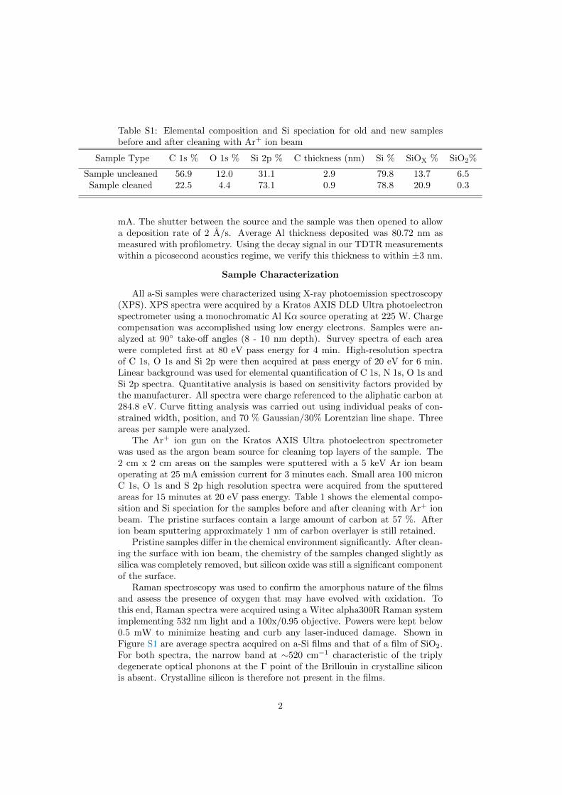
Table S1: Elemental composition and Si speciation for old and new samplesbefore and after cleaning with Ar+ ion beam
Sample Type C 1s % O 1s % Si 2p % C thickness (nm) Si % SiOX % SiO2%
Sample uncleaned 56.9 12.0 31.1 2.9 79.8 13.7 6.5Sample cleaned 22.5 4.4 73.1 0.9 78.8 20.9 0.3
mA. The shutter between the source and the sample was then opened to allowa deposition rate of 2 A/s. Average Al thickness deposited was 80.72 nm asmeasured with profilometry. Using the decay signal in our TDTR measurementswithin a picosecond acoustics regime, we verify this thickness to within ±3 nm.
Sample Characterization
All a-Si samples were characterized using X-ray photoemission spectroscopy(XPS). XPS spectra were acquired by a Kratos AXIS DLD Ultra photoelectronspectrometer using a monochromatic Al Kα source operating at 225 W. Chargecompensation was accomplished using low energy electrons. Samples were an-alyzed at 90◦ take-off angles (8 - 10 nm depth). Survey spectra of each areawere completed first at 80 eV pass energy for 4 min. High-resolution spectraof C 1s, O 1s and Si 2p were then acquired at pass energy of 20 eV for 6 min.Linear background was used for elemental quantification of C 1s, N 1s, O 1s andSi 2p spectra. Quantitative analysis is based on sensitivity factors provided bythe manufacturer. All spectra were charge referenced to the aliphatic carbon at284.8 eV. Curve fitting analysis was carried out using individual peaks of con-strained width, position, and 70 % Gaussian/30% Lorentzian line shape. Threeareas per sample were analyzed.
The Ar+ ion gun on the Kratos AXIS Ultra photoelectron spectrometerwas used as the argon beam source for cleaning top layers of the sample. The2 cm x 2 cm areas on the samples were sputtered with a 5 keV Ar ion beamoperating at 25 mA emission current for 3 minutes each. Small area 100 micronC 1s, O 1s and S 2p high resolution spectra were acquired from the sputteredareas for 15 minutes at 20 eV pass energy. Table 1 shows the elemental compo-sition and Si speciation for the samples before and after cleaning with Ar+ ionbeam. The pristine surfaces contain a large amount of carbon at 57 %. Afterion beam sputtering approximately 1 nm of carbon overlayer is still retained.
Pristine samples differ in the chemical environment significantly. After clean-ing the surface with ion beam, the chemistry of the samples changed slightly assilica was completely removed, but silicon oxide was still a significant componentof the surface.
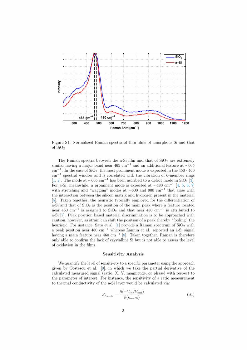
Raman spectroscopy was used to confirm the amorphous nature of the filmsand assess the presence of oxygen that may have evolved with oxidation. Tothis end, Raman spectra were acquired using a Witec alpha300R Raman systemimplementing 532 nm light and a 100x/0.95 objective. Powers were kept below0.5 mW to minimize heating and curb any laser-induced damage. Shown inFigure S1 are average spectra acquired on a-Si films and that of a film of SiO2.For both spectra, the narrow band at ∼520 cm−1 characteristic of the triplydegenerate optical phonons at the Γ point of the Brillouin in crystalline siliconis absent. Crystalline silicon is therefore not present in the films.
2
300 400 500 600 700 800 900 1000 1100 1200Raman Shift [cm−1]
Inte
nsity
465 cm−1 480 cm−1
SiO2a−Si
Figure S1: Normalized Raman spectra of thin films of amorphous Si and thatof SiO2
The Raman spectra between the a-Si film and that of SiO2 are extremelysimilar having a major band near 465 cm−1 and an additional feature at ∼605cm−1. In the case of SiO2, the most prominent mode is expected in the 450 - 460cm−1 spectral window and is correlated with the vibration of 6-member rings[1, 2]. The mode at ∼605 cm−1 has been ascribed to a defect mode in SiO2 [3].For a-Si, meanwhile, a prominent mode is expected at ∼480 cm−1 [4, 5, 6, 7]with stretching and “wagging” modes at ∼600 and 900 cm−1 that arise withthe interaction between the silicon matrix and hydrogen present in the material[5]. Taken together, the heuristic typically employed for the differentiation ofa-Si and that of SiO2 is the position of the main peak where a feature locatednear 460 cm−1 is assigned to SiO2 and that near 480 cm−1 is attributed toa-Si [7]. Peak position based material discrimination is to be approached withcaution, however, as strain can shift the position of a peak thereby “fooling” theheuristic. For instance, Sato et al. [1] provide a Raman spectrum of SiO2 witha peak position near 480 cm−1 whereas Lannin et al. reported an a-Si signalhaving a main feature near 460 cm−1 [8]. Taken together, Raman is thereforeonly able to confirm the lack of crystalline Si but is not able to assess the levelof oxidation in the films.
Sensitivity Analysis
We quantify the level of sensitivity to a specific parameter using the approachgiven by Costescu et al. [9], in which we take the partial derivative of thecalculated measured signal (ratio, X, Y, magnitude, or phase) with respect tothe parameter of interest. For instance, the sensitivity of a ratio measurementto thermal conductivity of the a-Si layer would be calculated via:
Sκa−Si=∂(−Vin/Vout)∂(κa−Si)
(S1)
3
0 1 2 3 4 5 60 . 0
0 . 1
0 . 2
0 . 3
0 . 4
0 . 5
κa - S i
h K , a - S i / c - S i
Sen
sitivit
y of R
atio (-X
/Y)
T i m e D e l a y ( n s )
h K , A l / a - S i
0 1 2 3 4 5 60 . 0
0 . 1
0 . 2
0 . 3
0 . 4
h K , A l / a - S ih K , a - S i / c - S i
κa - S i
Sensiti
vity o
f Ratio
(-X/Y)
T i m e D e l a y ( n s )
(a) 10 nm a-Si Sensitivity (b) 200 nm a-Si Sensitivity
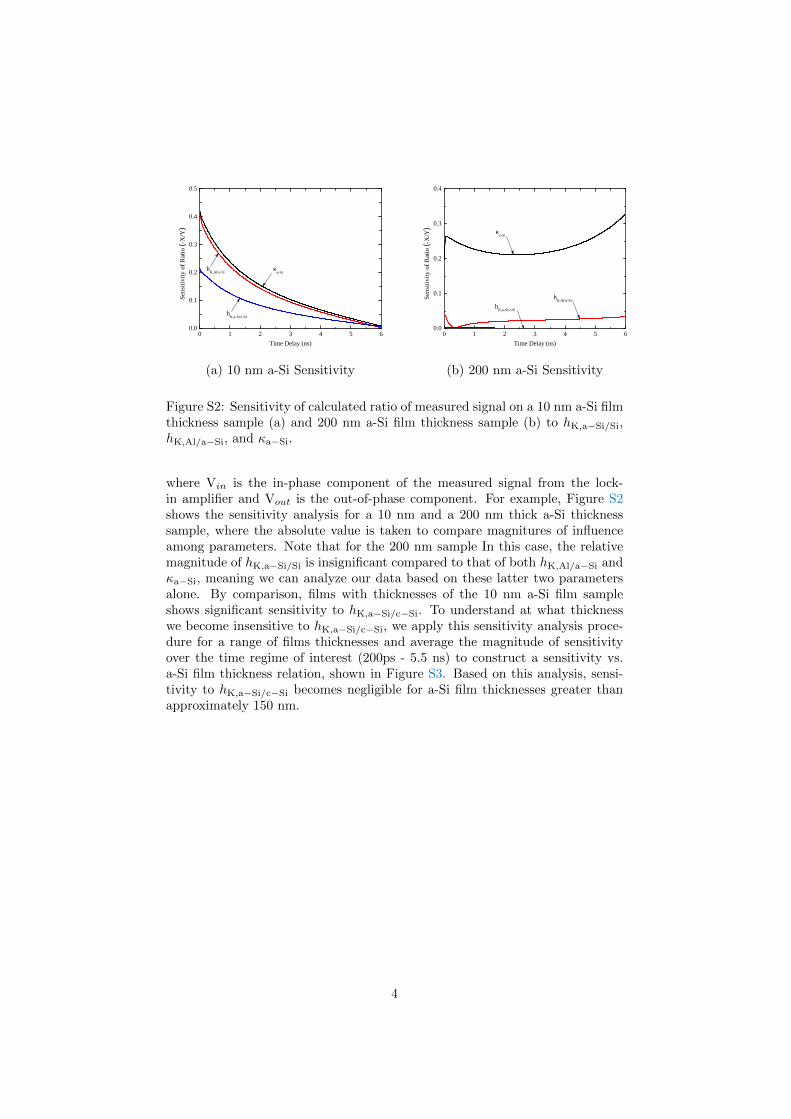
Figure S2: Sensitivity of calculated ratio of measured signal on a 10 nm a-Si filmthickness sample (a) and 200 nm a-Si film thickness sample (b) to hK,a−Si/Si,hK,Al/a−Si, and κa−Si.
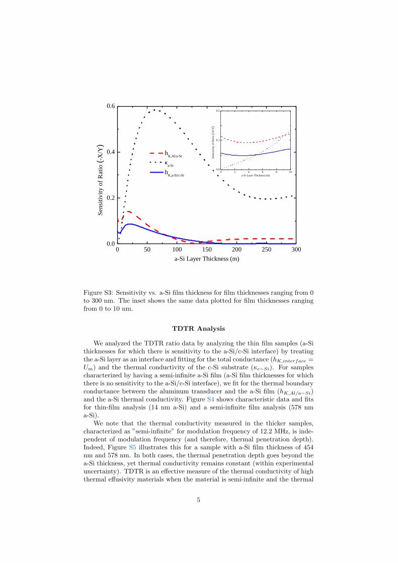
where Vin is the in-phase component of the measured signal from the lock-in amplifier and Vout is the out-of-phase component. For example, Figure S2shows the sensitivity analysis for a 10 nm and a 200 nm thick a-Si thicknesssample, where the absolute value is taken to compare magnitures of influenceamong parameters. Note that for the 200 nm sample In this case, the relativemagnitude of hK,a−Si/Si is insignificant compared to that of both hK,Al/a−Si andκa−Si, meaning we can analyze our data based on these latter two parametersalone. By comparison, films with thicknesses of the 10 nm a-Si film sampleshows significant sensitivity to hK,a−Si/c−Si. To understand at what thicknesswe become insensitive to hK,a−Si/c−Si, we apply this sensitivity analysis proce-dure for a range of films thicknesses and average the magnitude of sensitivityover the time regime of interest (200ps - 5.5 ns) to construct a sensitivity vs.a-Si film thickness relation, shown in Figure S3. Based on this analysis, sensi-tivity to hK,a−Si/c−Si becomes negligible for a-Si film thicknesses greater thanapproximately 150 nm.
4
0 5 0 1 0 0 1 5 0 2 0 0 2 5 0 3 0 00 . 0
0 . 2
0 . 4
0 . 6
0 2 4 6 8 1 00 . 0
0 . 1
0 . 2
h K , A l / a - S i κa - S i h K , a - S i / c - S i
Sen
sitivit
y of R
atio (-X
/Y)
a - S i L a y e r T h i c k n e s s ( m )
Sensi
tivity
of Ra
tio (-X
/Y)
a - S i L a y e r T h i c k n e s s ( m )
Figure S3: Sensitivity vs. a-Si film thickness for film thicknesses ranging from 0to 300 nm. The inset shows the same data plotted for film thicknesses rangingfrom 0 to 10 nm.
TDTR Analysis
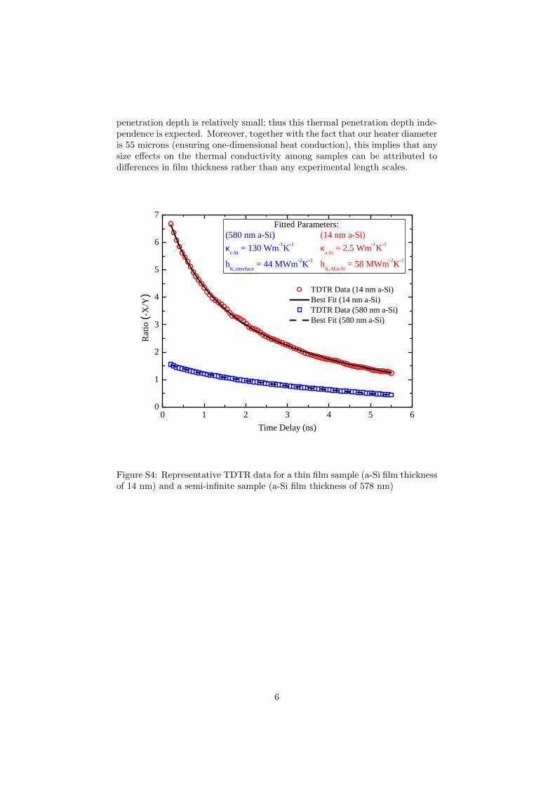
We analyzed the TDTR ratio data by analyzing the thin film samples (a-Sithicknesses for which there is sensitivity to the a-Si/c-Si interface) by treatingthe a-Si layer as an interface and fitting for the total conductance (hK,interface =Um) and the thermal conductivity of the c-Si substrate (κc−Si). For samplescharacterized by having a semi-infinite a-Si film (a-Si film thicknesses for whichthere is no sensitivity to the a-Si/c-Si interface), we fit for the thermal boundaryconductance between the aluminum transducer and the a-Si film (hK,Al/a−Si)and the a-Si thermal conductivity. Figure S4 shows characteristic data and fitsfor thin-film analysis (14 nm a-Si) and a semi-infinite film analysis (578 nma-Si).
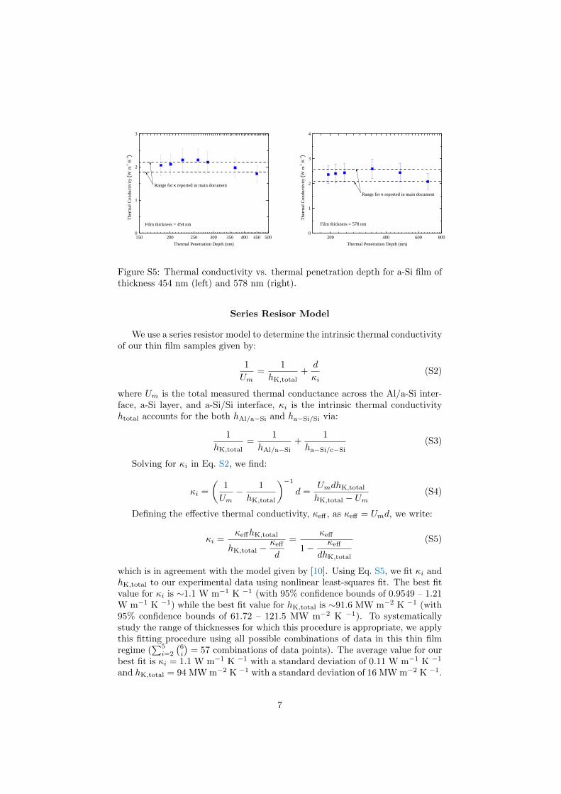
We note that the thermal conductivity measured in the thicker samples,characterized as ”semi-infinite” for modulation frequency of 12.2 MHz, is inde-pendent of modulation frequency (and therefore, thermal penetration depth).Indeed, Figure S5 illustrates this for a sample with a-Si film thickness of 454nm and 578 nm. In both cases, the thermal penetration depth goes beyond thea-Si thickness, yet thermal conductivity remains constant (within experimentaluncertainty). TDTR is an effective measure of the thermal conductivity of highthermal effusivity materials when the material is semi-infinite and the thermal
5
penetration depth is relatively small; thus this thermal penetration depth inde-pendence is expected. Moreover, together with the fact that our heater diameteris 55 microns (ensuring one-dimensional heat conduction), this implies that anysize effects on the thermal conductivity among samples can be attributed todifferences in film thickness rather than any experimental length scales.
0 1 2 3 4 5 60
1
2
3
4
5
6
7( 1 4 n m a - S i )κa - S i = 2 . 5 W m - 1 K - 1
h K , A l / a - S i = 5 8 M W m - 2 K - 1
( 5 8 0 n m a - S i )κc - S i = 1 3 0 W m - 1 K - 1
h K , i n t e r f a c e = 4 4 M W m - 2 K - 1
T D T R D a t a ( 1 4 n m a - S i ) B e s t F i t ( 1 4 n m a - S i ) T D T R D a t a ( 5 8 0 n m a - S i ) B e s t F i t ( 5 8 0 n m a - S i )
Ratio
(-X/Y)
T i m e D e l a y ( n s )
F i t t e d P a r a m e t e r s :
Figure S4: Representative TDTR data for a thin film sample (a-Si film thicknessof 14 nm) and a semi-infinite sample (a-Si film thickness of 578 nm)
6
1 5 0 2 0 0 2 5 0 3 0 0 3 5 0 4 0 0 4 5 0 5 0 00
1
2
3
Therm
al Cond
uctivi
ty (W
m-1 K-1 )
T h e r m a l P e n e t r a t i o n D e p t h ( n m )
R a n g e f o r κ r e p o r t e d i n m a i n d o c u m e n t
F i l m t h i c k n e s s = 4 5 4 n m
2 0 0 4 0 0 6 0 0 8 0 00
1
2
3
4
F i l m t h i c k n e s s = 5 7 8 n m
R a n g e f o r κ r e p o r t e d i n m a i n d o c u m e n t
Therm
al Cond
uctivi
ty (W
m-1 K-1 )
T h e r m a l P e n e t r a t i o n D e p t h ( n m )
Figure S5: Thermal conductivity vs. thermal penetration depth for a-Si film ofthickness 454 nm (left) and 578 nm (right).
Series Resisor Model
We use a series resistor model to determine the intrinsic thermal conductivityof our thin film samples given by:
1
Um=
1
hK,total+
d
κi(S2)
where Um is the total measured thermal conductance across the Al/a-Si inter-face, a-Si layer, and a-Si/Si interface, κi is the intrinsic thermal conductivityhtotal accounts for the both hAl/a−Si and ha−Si/Si via:
1
hK,total=
1
hAl/a−Si+
1
ha−Si/c−Si(S3)
Solving for κi in Eq. S2, we find:
κi =
(1
Um− 1
hK,total
)−1
d =UmdhK,total
hK,total − Um(S4)
Defining the effective thermal conductivity, κeff , as κeff = Umd, we write:
κi =κeffhK,total
hK,total −κeff
d
=κeff
1− κeff
dhK,total
(S5)
which is in agreement with the model given by [10]. Using Eq. S5, we fit κi andhK,total to our experimental data using nonlinear least-squares fit. The best fitvalue for κi is ∼1.1 W m−1 K −1 (with 95% confidence bounds of 0.9549 – 1.21W m−1 K −1) while the best fit value for hK,total is ∼91.6 MW m−2 K −1 (with95% confidence bounds of 61.72 – 121.5 MW m−2 K −1). To systematicallystudy the range of thicknesses for which this procedure is appropriate, we applythis fitting procedure using all possible combinations of data in this thin filmregime (
∑5i=2
(6i
)= 57 combinations of data points). The average value for our
best fit is κi = 1.1 W m−1 K −1 with a standard deviation of 0.11 W m−1 K −1
and hK,total = 94 MW m−2 K −1 with a standard deviation of 16 MW m−2 K −1.
7
The only outlier to this best fit value for thermal conductivity came for thecombination of 3 and 7 nm films, for which κi = 1.6 W m−1 K −1 and hK,total =87 MW m−2 K −1 . While this may suggest the assumption of constant thermalconductivity fails for these films, it is not possible to draw a solid conclusion.This discrepancy may be a result of the very narrow range (film thicknessesonly separated by 4 nm) over which to fit. Moreover, the sensitivity to hK,total
in this regime is extremely high, meaning that any fluctuations to this valuewill drastically influence the fitted value for κi. Indeed, the fitted value hK,total
is within a standard deviation of the mean of all fitted hK,total, κi, yet κi asfitted is almost five standard deviations above the mean for all κi. Removingthese two data points does not significantly influence the results; we calculateκi = 1.12 W m−1 K −1 and hK,total = 82 MW m−2 K −1, shifting our derivedthermal conductivities up in magnitude only 5%.
Using the same procedure on our a-SiO2 films, we find the best fit value forκi is ∼1.4 W m−1 K −1 (with 95% confidence bounds of 1.2802 – 1.526 W m−1
K −1) while the best fit value for hK,total is ∼180 MW m−2 K −1 (with 95%confidence bounds of 124.9 – 135.4 MW m−2 K −1).
Impurity and umklapp Scattering Relaxation Times
The relaxation times used to describe the scattering events in a propagon-dominated a-Si system are based on the equation for impurity and umklappscattering in bulk crystalline silicon:
1
τ= Aω4 +BTω2 exp
(−CT
)(S6)
where τ is the relaxation time. The first term in Eq. S6 describes impurity scat-tering, while the second term describes umklapp scattering. Normal scatteringis not included since we are experimenting at room temperature; at tempera-tures, T, such that T ≥ 0.1θD, where θD is the Debye temperature, umklappscattering dominates over normal scattering such that normal scattering canbe neglected[11]. The thermal conductivity of bulk crystalline silicon can becalculated using a kinetic theory model:
κSi =1
3
∑j
ωmax,j∫0
~ωDj(ω)∂f
∂Tv2j τjdω (S7)
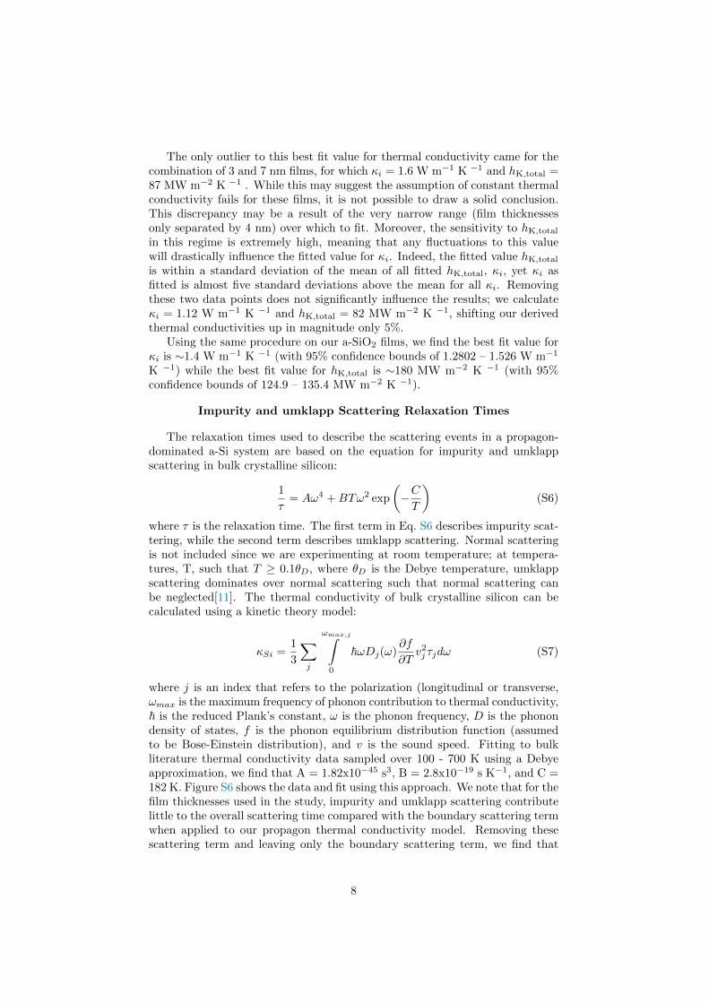
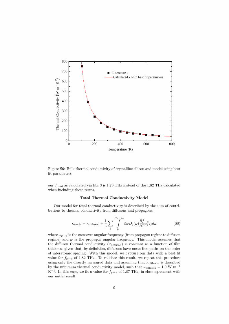
where j is an index that refers to the polarization (longitudinal or transverse,ωmax is the maximum frequency of phonon contribution to thermal conductivity,~ is the reduced Plank’s constant, ω is the phonon frequency, D is the phonondensity of states, f is the phonon equilibrium distribution function (assumedto be Bose-Einstein distribution), and v is the sound speed. Fitting to bulkliterature thermal conductivity data sampled over 100 - 700 K using a Debyeapproximation, we find that A = 1.82x10−45 s3, B = 2.8x10⁻¹⁹ s K−1, and C =182 K. Figure S6 shows the data and fit using this approach. We note that for thefilm thicknesses used in the study, impurity and umklapp scattering contributelittle to the overall scattering time compared with the boundary scattering termwhen applied to our propagon thermal conductivity model. Removing thesescattering term and leaving only the boundary scattering term, we find that
8
0 2 0 0 4 0 0 6 0 0 8 0 00
1 0 0
2 0 0
3 0 0
4 0 0
5 0 0
6 0 0
7 0 0
8 0 0
L i t e r a t u r e κ C a l c u l a t e d κ w i t h b e s t f i t p a r a m e t e r s
Th
ermal C
onduct
ivity
(W m
-1 K-1 )
T e m p e r a t u r e ( K )
Figure S6: Bulk thermal conductivity of crystalline silicon and model using bestfit parameters
our fp→d as calculated via Eq. 3 is 1.70 THz instead of the 1.82 THz calculatedwhen including these terms.
Total Thermal Conductivity Model
Our model for total thermal conductivity is described by the sum of contri-butions to thermal conductivity from diffusons and propagons:
κa−Si = κdiffuson +1
3
∑j
ωp→d,j∫0
~ωDj(ω)∂f
∂Tv2j τjdω (S8)
where ωp→d is the crossover angular frequency (from propagon regime to diffusonregime) and ω is the propagon angular frequency. This model assumes thatthe diffuson thermal conductivity (κdiffuson) is constant as a function of filmthickness given that, by definition, diffusons have mean free paths on the orderof interatomic spacing. With this model, we capture our data with a best fitvalue for fp→d of 1.82 THz. To validate this result, we repeat this procedureusing only the directly measured data and assuming that κdiffuson is describedby the minimum thermal conductivity model, such that κdiffuson = 1.0 W m−1
K−1. In this case, we fit a value for fp→d of 1.87 THz, in close agreement withour initial result.
9
Molecular Dynamics: a-Si Thermal Conductivity in ac-Si/a-SiO2/a-Si System
We performed molecular dynamics simulations of the c-Si/a-SiO2/a-Si sys-tem to investigate the trend of a-Si thermal conductivity with thickness. Fig-ure S7 shows a schematic of the system. All simulations were performed inLAMMPS [12], had boundaries periodic in the x and y directions, used atime step of 0.5 fs, and used a Tersoff potential for atomic interactions [13] witha modified form of the cutoff function [14]. Domain creation consisted of twosteps: vitrification of a 1 nm native oxide layer [15], and the creation and joiningof a-Si of various thicknesses to the c-Si/a-SiO2 system. Unless otherwise stated,the system was run in the NVT ensemble (constant number, volume, tempera-ture) with temperatures controlled by a Nose-Hoover thermostat [16, 17] witha coupling time of 1 ps. Three system geometries were investigated. In geom-etry A, the initial system consisted of 5×5×200 unit cells of c-Si, capped by5×3×1.22 unit cells of strained SiO2 in the tridymite phase, with the c-axisparallel to c-Si [001]. The c-Si lattice constant was set to 5.43097 A, causing acompressive strain of about −0.004 at 300 K.
The SiO2 was heated to 4500 K for 100 ps while the c-Si was held at 300 K.The SiO2 was then quenched at 10 K/ps back to 300 K. Separate from the c-Si/SiO2 system, a 5×5×N unit cell block of Si (N–7=9, 15, 23, 37, 58, 1461) washeated from 300 K to 4500 K over 50 ps, held at 4500 K for 75 ps, then quenchedto 300 K at 10 K/ps. The newly formed a-Si was then joined to the c-Si/a-SiO2
by placing the two domains spatially adjacent to each other and giving the a-Sia velocity of 0.1 A/ps towards the c-Si/a-SiO2. During the joining, the wholesystem was annealed at 2000 K for 200 ps and the system momentum was zeroedevery 10 ps after 40 ps had passed to minimize undesired acoustic oscillations.After annealing, the system was re-cooled to 300 K at 10 K/ps. Finally, thewhole system was equilibrated for 100 ps with an imposed temperature profileclose to that expected for the steady state of the non-equilibrium measurementof thermal conductivity. That is, the c-Si portion was kept at 300 K and thea-SiO2 and a-Si portions had a linear temperature gradient from 300 K to 340 Kimposed on them by a Langevin thermostat [18] with a coupling time of 1 ps.
System geometries B and C explored size effects other than the thickness.In geometry B, the dependence of thermal conductivity on total system length,not just a-Si thickness, was investigated by setting the c-Si and a-Si thicknessesto 151 and 58 unit cells, respectively. This gave the system a total length equalto the 9 unit cell geometry A simulation. In geometry C, the effect of the cross-sectional dimensions was investigated by setting the c-Si and a-Si thicknesses to40 and 58 unit cells, respectively, and the cross-sectional dimensions to 6 and8 unit cells. In this case, the a-SiO2 was formed from a 6×5×1.22 unit cell blockof strained tridymite-SiO2.2
After the domain creation, data were collected with the following procedure.End walls were imposed on both sides and a 2×2 array of cones with radiiof 0.68 nm and height 2.72 nm were made by immobilizing atoms to mitigateundesired size effects (Figure S7) [19]. The 2 nm thick cold and hot bathsmaintained temperatures of 300 K and 340 K, respectively, using a Langevinthermostat [18] with a coupling time of 1 ps. The Langevin thermostat is
1The N–7 term accounts for the wall and cones, see following paragraph2The cone radii were adjusted to form a 3×4 array of cones, see following paragraph.
10
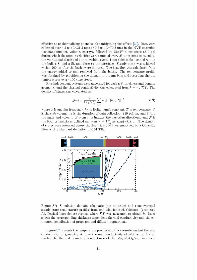
effective at re-thermalizing phonons, also mitigating size effects [20]. Data werecollected over 4.5 ns (L≤31.5 nm) or 9.5 ns (L=79.3 nm) in the NVE ensemble(constant number, volume, energy), followed by 25×216 times steps (819 ps)during which the atomic velocities were sampled every 25 time steps to calculatethe vibrational density of states within several 1 nm thick slabs located withinthe bulk c-Si and a-Si, and close to the interface. Steady state was achievedwithin 200 ps after the baths were imposed. The heat flux was calculated fromthe energy added to and removed from the baths. The temperature profilewas obtained by partitioning the domain into 1 nm bins and recording the bintemperatures every 100 time steps.
Five independent systems were generated for each a-Si thickness and domaingeometry, and the thermal conductivity was calculated from k = −q/∇T . Thedensity of states was calculated as:
g(ω) =2
kBTV tf
∑i,α
mi|F [ui,α(t)] |2 (S9)
where ω is angular frequency, kB is Boltzmann’s constant, T is temperature, Vis the slab volume, tf is the duration of data collection (819 ps), mi and ui arethe mass and velocity of atom i, α indexes the cartesian directions, and F isthe Fourier transform defined as: F [h(t)] ≡
∫∞−∞ h(t)exp(−iωt)dt. The density
of states were averaged across the five trials and then smoothed by a Gaussianfilter with a standard deviation of 0.01 THz.
0 50 100 150 200300
310
320
330
340
z, nm
tem
pera
ture
,K
0 20 40 60 800
1
2 kp ; f ≤ 2.5 THz
kp ; f > 2.5 THzkd ; r > 2 nm
kd ; r ≤ 2 nm
a-Si thickness, nm
k,W
m−1K−1
wall bath c-Si a-SiO2 a-Si bath wall
Figure S7: Simulation domain schematic (not to scale) and time-averagedsteady-state temperature profiles from one trial for each thickness (geometryA). Dashed lines denote regions where ∇T was measured to obtain k. Insetshows the corresponding thickness-dependent thermal conductivity and the es-timated contribution of propagon and diffuson populations.
Figure S7 presents the temperature profiles and thickness-dependent thermalconductivity of geometry A. The thermal conductivity of a-Si is too low toresolve the thermal boundary conductance of the c-Si/a-SiO2/a-Si interface.
11
The strain of about -0.004 has a negligible effect on the thermal conductivitycompared to an unstrained system [21]. The thermal conductivity of geometry Bwas 1.64±0.09 Wm−1K−1, the same as geometry A for the same a-Si thickness.Thus, the calculated thermal conductivity depends only on the a-Si thickness.The thermal conductivity of geometry C was 1.63±0.04 Wm−1K−1, so the effectof the cross-section is negligible for dimensions on the order of a few nanometers.
We roughly estimate the contribution by propagons and diffusons of dif-ferent frequencies and length-scales to the thermal conductivity as plotted inFigure S7. The contribution by propagons with frequencies below 2.5 THz (red)is calculated by Equation S20 with vT and vL equal to 3.9 and 7.9 nm/ps, re-spectively, and the same scattering coefficients as used in Equation S19. Thedensity of states shows that all modes below 2.5 THz are propagons (Figure S8).The smallest a-Si thickness studied was 5 nm. Since diffusons transmit energyby the coupling of adjacent modes, only modes with a characteristic lengthscale, or radius r, of roughly 2 nm or less can contribute to the thermal conduc-tivity of 5 nm a-Si, and this contribution (blue) should remain constant witha-Si length. As the a-Si becomes thicker, diffuson modes with larger radii maycontribute, along with any propagons that are present above 2.5 THz (green).The initial rise in the total thermal conductivity is therefore likely due to largerscale diffuson modes becoming accessible as the sample lengthens. Prior sim-ulation results show that the participation ratio of diffuson modes can remainsignificant out to 2 nm [22]. Over the whole thickness range, the contributionof low-frequency propagons increases as their mean-free-paths lengthen. Thick-nesses greater than 80 nm become difficult to simulate due to the time scalesaccessible to simulations.
0 1 2 3 4 50
5
10
15
frequency, THz
dens
ityof
stat
es,st
ates·n
m−3T
Hz−1
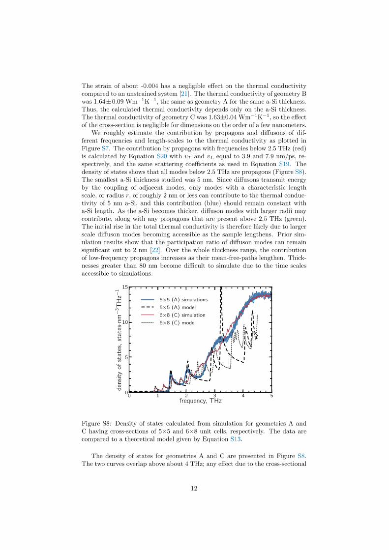
5×5 (A) simulations5×5 (A) model6×8 (C) simulation6×8 (C) model
Figure S8: Density of states calculated from simulation for geometries A andC having cross-sections of 5×5 and 6×8 unit cells, respectively. The data arecompared to a theoretical model given by Equation S13.
The density of states for geometries A and C are presented in Figure S8.The two curves overlap above about 4 THz; any effect due to the cross-sectional
12
dimension therefore occur below 4 THz. The data for geometry A below about2.5 THz is well fit by a quasi-1D model (Equation S13), in agreement with thepropagon-diffuson crossover of 2.4 THz for a-Si calculated by Allen et al. [22].The first and second peaks are due to transverse propagons with a sound speed of3.9 nm/ps and integral wavenumbers (nx,ny) = (±1,0) or (0,±1) and (±1,±1),respectively. The data and model for geometry C begin to diverge at about2.0 THz. It is possible that as the cross-sectional dimensions are increased,the cross-over frequency would approach a finite constant that agrees with theexperiment. Even so, the low frequency trend in the simulated density of statesmarkedly differs from the 3-D Debye density of states, indicating that the sizeeffects exhibited in the molecular dynamics simulation should not be assumedto have the same form as in experiment.
The quasi-1D density of states exhibited in these simulations will mattermost for simulations of glasses and alloys, where the low frequency energy carri-ers may contribute a significant amount to the total thermal conductivity. Suchsimulations may not recreate the vibrational physics relevant to transport inthe experimental system. Furthermore, the cross-sectional dimensions of about2.7 nm for geometry A are less than the effective radius of many extended dif-fuson modes [22], which might introduce additional size effects into the diffusonpopulation which would not be present in the experimental system. Neverthe-less, the a-Si thermal conductivity exhibits a clear length dependence up tothe thickest samples investigated (Figure S7). One notes, however, that thisincrease becomes less significant as film thickness increases, such that thermalconductivity (specifically the contribution from diffusons) shows an asymptopictrend as film thickness increases.
We caution that the MD-predicted thermal conductivities for amorphousmaterials depend on the sample preparation method such as the melt-quenchprocedure and annealing time implemented during sample preparation. To thisend, we have conducted additional NEMD simulations on isolated amorphousSi (with thicknesses similar to those used for the system geometries reportedabove) prepared after annealing at 1100 K for 10 ns. This results in the removalof metastability as evident from the decrease and plateau in the sample poten-tial energy. Further, we use a relatively slower quench rate of 0.3 K/ps duringour sample preparation. The thermal conductivities for the structures preparedwith this procedure are slightly lower than those reported for the above geome-tries, however, the trends in the increase in thermal conductivity with samplethickness remains unchanged.
13
Quasi One Dimensional Density of States
In this section we derive the phonon density of states for a quasi one dimen-sional system, for which the wavenumbers in the x and y directions may onlytake on discrete values. The number of states between kz and kz + dkz for atrue one dimensional system is:
N(kz) = 2L
2πdkz (S10)
where kz is the wavevector in the one direction permitted in the one dimensionalsystem, and L is the length of the system. Now, expanding the one dimensionalsystem in the cross-sectional direction so that the x and y boundaries are peri-odic and not too long, the Debye approximation gives a phonon dispersion:
ω = vj
√k2x + k2
y + k2z (S11)
where vj is the group velocity of the jth polarization. Because of the periodicboundaries, kx may only take on values of 2πnx/Lx, where nx is an integerand Lx is the length of the system in the x direction, and likewise for ky. Thenumber of states between ω and ω + dω is thus:
N(ω) =L
π
ω
v2j
[ω2
v2j
−(k2x + k2
y
)]− 12
dω (S12)
Normalizing by the system volume and the frequency interval; summing over
nx, ny, and j, and noticing that the minimal value of ω(kz) is vj√k2x + k2
y yields
the density of states as:
g(ω) =1
πLxLy
∑j
∑nx,ny
ω
v2j
[ω2
v2j
−(k2x + k2
y
)]− 12
H(ω − vj
√k2x + k2
y
)(S13)
where H(ξ) is the Heaviside function.
Confined Propagon Thermal Conductivity
The effect of confinement as evidenced by the low frequency density of states(Figure S8) affects the thickness-dependent thermal conductivity as calculatedby simulations (Figure S7). The contribution of the low frequency propagonspresent in the simulation domain may be estimated from a phonon transportcalculation approach. We assume that all energy carriers below a certain cutofffrequency are propagons that scatter with a rate that composites propagon-propagon scattering and propagon boundary scattering. We also use a Debyeapproximation. The heat flux of a quasi one-dimensional system is:
J =1
L
∑j
∑nx,ny,nz
vj,z~ωf (S14)
where L is the length of the quasi one-dimensional system, j indexes polariza-tions, nx,y,z are integers defining the wavevector, vz is the velocity in the axial
14
direction, ~ is the reduced Planck’s constant, ω is angular frequency, and f isthe phonon occupation. For a true one-dimensional system, there would be onlyone polarization and nx and ny would be restricted to zero.
Converting the sum over nz to an integral over wavenumber kz and splittingthe integral in two yields:
J =1
2π
∑j
∑nx,ny
{∫ 0
−∞vj,z~ωf2dkz +
∫ ∞0
vj,z~ωf1dkz
}(S15)
The left- and righthand integrals account for propagons traveling in thenegative and positive z directions, with populations of f2 and f1, respectively.The integrals over wavenumber can be converted to integrals over frequencyusing the Debye dispersion:
dkz =|k|vjkz
dω. (S16)
Since vj,z = vjkz|k| , Equation S15 becomes:
J =1
2π
∑j
∑nx,ny
{∫ ωmin
ωmax
~ωf2dω +
∫ ωmax
ωmin
~ωf1dω
}(S17)
where ωmin = vj√k2x + k2
y.
From kinetic theory [23], the difference in population between propagonstraveling in the positive and negative directions having the same frequency is,within a linear approximation, given by:
f1 − f2 = −τvz∂f0
∂T
∂T
∂z(S18)
where f0 is the equilibrium propagon distribution given by the Boltzmann dis-tribution for classical molecular dynamics. The relaxation time, τ , is modeledhaving contributions from boundary scattering and propagon-propagon scatter-ing:
τ =
[2vzL
+ATω2exp
(−BT
)]−1
(S19)
Finally, plugging Equation S18 into Equation S17, normalizing by the do-main’s cross-sectional area, and comparing to Fourier’s Law yields the finalresult:
kprop =1
2πLxLy
~2
kBT 2
∑j
∑nx,ny
∫ ωmax
vj√k2x+k2y
ωexp
(− ~ωkBT
)[ω2
v2j
−(k2x + k2
y
)] 12
v2j τdω
(S20)where kx,y = 2πnx,y/Lx,y, Lx and Ly are the cross-sectional dimensions and kBis Boltzmann’s constant.
15
References
[1] Tomoko Sato, Nobumasa Funamori, and Takehiko Yagi. Helium penetratesinto silica glass and reduces its compressibility. Nat Commun, 2:345, 062011. URL http://dx.doi.org/10.1038/ncomms1343.
[2] Frank L. Galeener. Band limits and the vibrational spectra of tetrahedralglasses. Phys. Rev. B, 19:4292–4297, Apr 1979. doi: 10.1103/PhysRevB.19.4292. URL http://link.aps.org/doi/10.1103/PhysRevB.19.4292.
[3] F. L. Galeener, R. A. Barrio, E. Martinez, and R. J. Elliott. Vibrationaldecoupling of rings in amorphous solids. Phys. Rev. Lett., 53:2429–2432,Dec 1984. doi: 10.1103/PhysRevLett.53.2429. URL http://link.aps.
org/doi/10.1103/PhysRevLett.53.2429.
[4] Dionisio Bermejo and Manuel Cardona. Raman scattering in pure and hy-drogenated amorphous germanium and silicon. Journal of Non-CrystallineSolids, 32(1–3):405 – 419, 1979. ISSN 0022-3093. doi: http://dx.doi.org/10.1016/0022-3093(79)90085-1. URL http://www.sciencedirect.com/
science/article/pii/0022309379900851. Electronic Properties andStructure of Amorphous Solids.
[5] M. H. Brodsky, Manuel Cardona, and J. J. Cuomo. Infrared and ramanspectra of the silicon-hydrogen bonds in amorphous silicon prepared byglow discharge and sputtering. Phys. Rev. B, 16:3556–3571, Oct 1977. doi:10.1103/PhysRevB.16.3556. URL http://link.aps.org/doi/10.1103/
PhysRevB.16.3556.
[6] F. L. Galeener and G. Lucovsky. Longitudinal optical vibrations inglasses: Geo2 and sio2. Phys. Rev. Lett., 37:1474–1478, Nov 1976.doi: 10.1103/PhysRevLett.37.1474. URL http://link.aps.org/doi/10.
1103/PhysRevLett.37.1474.
[7] Z Iqbal and S Veprek. Raman scattering from hydrogenated microcrys-talline and amorphous silicon. Journal of Physics C: Solid State Physics,15(2):377, 1982.
[8] J. S. Lannin, L. J. Pilione, S. T. Kshirsagar, R. Messier, and R. C. Ross.Variable structural order in amorphous silicon. Phys. Rev. B, 26:3506–3509,Sep 1982. doi: 10.1103/PhysRevB.26.3506. URL http://link.aps.org/
doi/10.1103/PhysRevB.26.3506.
[9] Ruxandra M. Costescu, Marcel A. Wall, and David G. Cahill. Thermalconductance of epitaxial interfaces. Phys. Rev. B, 67:054302, Feb 2003.doi: 10.1103/PhysRevB.67.054302. URL http://link.aps.org/doi/10.
1103/PhysRevB.67.054302.
[10] S.-M. Lee and David G. Cahill. Heat transport in thin dielectric films.Journal of Applied Physics, 81:2590, 1997.
[11] Glen A. Slack and S. Galginaitis. Thermal conductivity and phonon scat-tering by magnetic impurities in cdte. Phys. Rev., 133:A253–A268, Jan1964. doi: 10.1103/PhysRev.133.A253. URL http://link.aps.org/doi/
10.1103/PhysRev.133.A253.
16
[12] Steve Plimpton. Fast parallel algorithms for short-range molecular dy-namics. Journal of Computational Physics, 117(1):1 – 19, 1995. ISSN0021-9991. doi: http://dx.doi.org/10.1006/jcph.1995.1039. URL http:
//www.sciencedirect.com/science/article/pii/S002199918571039X.
[13] Shinji Munetoh, Teruaki Motooka, Koji Moriguchi, and Akira Shintani.Interatomic potential for si–o systems using tersoff parameterization. Com-putational Materials Science, 39(2):334 – 339, 2007. ISSN 0927-0256.doi: http://dx.doi.org/10.1016/j.commatsci.2006.06.010. URL http://
www.sciencedirect.com/science/article/pii/S0927025606002023.
[14] T. Kumagai, S. Izumi, S. Hara, and S. Sakai. Development of bond-orderpotentials that can reproduce the elastic constants and melting point ofsilicon for classical molecular dynamics simulation. Computational Mate-rials Science, 39(2):457 – 464, 2007. ISSN 0927-0256. doi: http://dx.doi.org/10.1016/j.commatsci.2006.07.013. URL http://www.sciencedirect.
com/science/article/pii/S0927025606002254.
[15] Yuhai Tu and J. Tersoff. Structure and energetics of the si- sio2 interface.Phys. Rev. Lett., 84:4393–4396, May 2000. doi: 10.1103/PhysRevLett.84.4393. URL http://link.aps.org/doi/10.1103/PhysRevLett.84.4393.
[16] Shuichi Nose. A unified formulation of the constant temperature moleculardynamics methods. The Journal of Chemical Physics, 81(1):511–519, 1984.URL http://scitation.aip.org/content/aip/journal/jcp/81/1/10.
1063/1.447334.
[17] William G. Hoover. Canonical dynamics: Equilibrium phase-space distri-butions. Phys. Rev. A, 31:1695–1697, Mar 1985. doi: 10.1103/PhysRevA.31.1695. URL http://link.aps.org/doi/10.1103/PhysRevA.31.1695.
[18] T. Schneider and E. Stoll. Molecular-dynamics study of a three-dimensionalone-component model for distortive phase transitions. Phys. Rev. B, 17:1302–1322, Feb 1978. doi: 10.1103/PhysRevB.17.1302. URL http://link.
aps.org/doi/10.1103/PhysRevB.17.1302.
[19] Zhi Liang and Pawel Keblinski. Finite-size effects on molecular dynamicsinterfacial thermal-resistance predictions. Phys. Rev. B, 90:075411, Aug2014. doi: 10.1103/PhysRevB.90.075411. URL http://link.aps.org/
doi/10.1103/PhysRevB.90.075411.
[20] K. Saaskilahti, J. Oksanen, J. Tulkki, and S. Volz. Role of anhar-monic phonon scattering in the spectrally decomposed thermal conduc-tance at planar interfaces. Phys. Rev. B, 90:134312, Oct 2014. doi: 10.1103/PhysRevB.90.134312. URL http://link.aps.org/doi/10.1103/
PhysRevB.90.134312.
[21] Kevin D. Parrish, Ankit Jain, Jason M. Larkin, Wissam A. Saidi, and AlanJ. H. McGaughey. Origins of thermal conductivity changes in strainedcrystals. Phys. Rev. B, 90:235201, Dec 2014. doi: 10.1103/PhysRevB.90.235201. URL http://link.aps.org/doi/10.1103/PhysRevB.90.235201.
17
[22] Philip B. Allen, Joseph L. Feldman, Jaroslav Fabian, and FrederickWooten. Diffusons, locons, propagons: Character of atomic vibrations inamorphous si. Philosophical Magazine B, 79:1715, 1999.
[23] Gang Chen. Nanoscale Energy Transport and Conversion: A ParallelTreatment of Electrons, Molecules, Phonons, and Photons. Oxford Uni-versity Press, USA, 2005.
18