Surface modifications of cellulose nanocrystals for biobased ...
Silicon nanocrystals on bottleresonators: Mode structure, loss
mechanisms and emission dynamics
P. Bianucci1,∗, X. Wang1,3, J. G. C. Veinot2 and A. Meldrum1,3
1Department of Physics, University of Alberta, Edmonton AB, T6G 2G7, Canada2Department of Chemistry, University of Alberta, Edmonton AB, T6G 2G2, Canada
3National Institute for Nanotechnology, National Research Council, Edmonton AB, T6G 2M9,Canada
Abstract: Bottle resonators can support high Q-factor whispering gallerymodes (WGMs) and demonstrate a rich mode spectrum. Resonators werefabricated using a fiber tapering apparatus and were coated with a thin,smooth layer of luminescent silicon nanocrystals. The photoluminescencespectrum showed WGM peaks with Q-factors near 2,500; however, evanes-cent measurements showed that these modes are a composite of many modeswith Q-factors exceeding 106, the highest yet seen for a silicon-nanocrystal-coated microresonators. The mode structure showed strong polarization andsensitivity to position within the bottle resonator. An analysis of loss mech-anisms establishes surface roughness scattering as the limiting factor inthese nanocrystal-coated bottle resonators in the absence of excited carriers.
© 2010 Optical Society of America
OCIS codes: (230.5750) Resonators; (140.3948) Microcavity devices; (250.5230) Photolumi-nescence.
References and links1. L. Pavesi, “Silicon-Based light sources for silicon integrated circuits,” Adv. Opt. Technol. 2008, 416926 (2008).2. D. Jurbergs, E. Rogojina, L. Mangolini, and U. Kortshagen, “Silicon nanocrystals with ensemble quantum yields
exceeding 60%,” Appl. Phys. Lett. 88, 233116 (2006).3. L. Pavesi, L. Dal Negro, C. Mazzoleni, G. Franzo, and F. Priolo, “Optical gain in silicon nanocrystals,” Nature
408, 440–444 (2000).4. M. Cazzanelli, D. Navarro-Urrıos, F. Riboli, N. Daldosso, L. Pavesi, J. Heitmann, L. X. Yi, R. Scholz,
M. Zacharias, and U. Gosele, “Optical gain in monodispersed silicon nanocrystals,” J. Appl. Phys. 96, 3164–3171 (2004).
5. A. Polman and R. G. Elliman, Towards the first silicon laser, vol. 93 of NATO Science Series (Kluwer AcademicPublishers, The Netherlands, 2003).
6. P. Fauchet, J. Ruan, H. Chen, L. Pavesi, L. Dal Negro, M. Cazzaneli, R. Elliman, N. Smith, M. Samoc, andB. Luther-Davies, “Optical gain in different silicon nanocrystal systems,” Opt. Mater. 27, 745–749 (2005).
7. P. Bianucci, J. R. Rodrıguez, C. M. Clements, J. G. C. Veinot, and A. Meldrum, “Silicon nanocrystal lumines-cence coupled to whispering gallery modes in optical fibers,” J. Appl. Phys. 105, 023108 (2009).
8. H. Chen, J. Sung, A. Tewary, M. Brongersma, J. Shin, and P. Fauchet, “Evidence for stimulated emission in sil-icon nanocrystal microspheres,” in “Group IV Photonics, 2005. 2nd IEEE International Conference on,” (2005),pp. 99–101.
9. A. Beltaos and A. Meldrum, “Whispering gallery modes in silicon-nanocrystal-coated silica microspheres,” J.Lumin. 126, 607–613 (2007).
10. A. Tewary, M. J. F. Digonnet, J. Sung, J. H. Shin, and M. L. Brongersma, “Silicon-Nanocrystal-Coated silicamicrosphere thermooptical switch,” IEEE J. Sel. Top. Quantum Electron. 12, 1476–1479 (2006).
11. R. D. Kekatpure and M. L. Brongersma, “Fundamental photophysics and optical loss processes in si-nanocrystal-doped microdisk resonators,” Phys. Rev. A 78, 023829 (2008).
#124171 - $15.00 USD Received 12 Feb 2010; revised 1 Apr 2010; accepted 2 Apr 2010; published 7 Apr 2010(C) 2010 OSA 12 April 2010 / Vol. 18, No. 8 / OPTICS EXPRESS 8466
12. M. Ghulinyan, D. Navarro-Urrıos, A. Pitanti, A. Lui, G. Pucker, and L. Pavesi, “Whispering-gallery modes andlight emission from a si-nanocrystal-based single microdisk resonator,” Opt. Express 16, 13218–13224 (2008).
13. C. Strelow, H. Rehberg, C. M. Schultz, H. Welsch, C. Heyn, D. Heitmann, and T. Kipp, “Optical microcavitiesformed by semiconductor microtubes using a bottlelike geometry,” Phys. Rev. Lett. 101, 127403 (2008).
14. S. Vicknesh, F. Li, and Z. Mi, “Optical microcavities on si formed by self-assembled InGaAs/GaAs quantum dotmicrotubes,” Appl. Phys. Lett. 94, 081101 (2009).
15. M. Pollinger, D. O’Shea, F. Warken, and A. Rauschenbeutel, “Ultra-high-Q tunable whispering-gallery-modemicroresonator,” Phys. Rev. Lett. 103, 053901 (2009).
16. G. Kakarantzas, T. E. Dimmick, T. A. Birks, R. L. Roux, and P. S. J. Russell, “Miniature all-fiber devices basedon CO2 laser microstructuring of tapered fibers,” Opt. Lett. 26, 1137–1139 (2001).
17. C. M. Hessel, M. A. Summers, A. Meldrum, M. Malac, and J. G. C. Veinot, “Direct patterning, conformal coating,and erbium doping of luminescent nc-si/sio2 thin films from solution processable hydrogen silsesquioxane,” Adv.Mater. 19, 3513–3516 (2007).
18. T. Kipp, H. Welsch, C. Strelow, C. Heyn, and D. Heitmann, “Optical modes in semiconductor microtube ringresonators,” Phys. Rev. Lett. 96, 077403 (2006).
19. Y. Rakovich, S. Balakrishnan, J. Donegan, T. Perova, R. Moore, and Y. Gun’ko, “The fabrication, fluorescencedynamics, and whispering gallery modes of aluminosilicate microtube resonators,” Adv. Funct. Mater. 17, 1106(2007).
20. L. Guimaraes and J. De Mendonca, “Analysis of the resonant scattering of light by cylinders at oblique inci-dence,” Appl. Opt. 36, 8010–8019 (1997).
21. P. Bianucci, J. Rodrıguez, F. Lenz, J. G. C. Veinot, and A. Meldrum, “Mode structure in the luminescence ofsi-nc in cylindrical microcavities,” Physica E 41, 1107 (2009).
22. Y. Louyer, D. Meschede, and A. Rauschenbeutel, “Tunable whispering-gallery-mode resonators for cavity quan-tum electrodynamics,” Phys. Rev. A 72, 031801 (2005).
23. I. Teraoka and S. Arnold, “Enhancing the sensitivity of a whispering-gallery mode microsphere sensor by ahigh-refractive-index surface layer,” J. Opt. Soc. Am. B 23, 1434–1441 (2006).
24. R. Kekatpure and M. Brongersma, “Quantification of free-carrier absorption in silicon nanocrystals with anoptical microcavity,” Nano. Lett. 8, 3787–3793 (2008).
25. F. P. Payne and J. P. R. Lacey, “A theoretical analysis of scattering loss from planar optical waveguides,” Opt.Quantum Electron. 26, 977–986 (1994).
26. J. R. Rodrıguez, P. Bianucci, A. Meldrum, and J. G. C. Veinot, “Whispering gallery modes in hollow cylindricalmicrocavities containing silicon nanocrystals,” Appl. Phys. Lett. 92, 131119 (2008).
27. N. Daldosso, M. Melchiorri, L. Pavesi, G. Pucker, F. Gourbilleau, S. Chausserie, A. Belarouci, X. Portier, andC. Dufour, “Optical losses and absorption cross-section of silicon nanocrystals,” J. Lumin. 121, 344 (2006).
28. J. D. Jackson, Classical electrodynamics; 3rd ed. (Wiley, New York, NY, 1998).29. A. Meldrum, P. Bianucci, and F. Marsiglio, “Purcell effect in inhomogenously broadened ensembles of quantum
dots coupled to optical microcavities,” (2010).30. L. Dal Negro, M. Cazzanelli, L. Pavesi, S. Ossicini, D. Pacifici, G. Franzo, F. Priolo, and F. Iacona, “Dynamics
of stimulated emission in silicon nanocrystals,” Appl. Phys. Lett. 82, 4636–4638 (2003).31. L. T. Canham, “Luminescence bands and their proposed origins in highly porous silicon,” Phys. Status Solidi B
190, 9–14 (1995).32. L. Tsybeskov, J. Vandyshev, and P. Fauchet, “Blue emission in porous silicon - oxygen-related photolumines-
cence,” Phys. Rev. B 49, 7821–7824 (1994).33. O. Schmidt, P. Kiesel, S. Mohta, and N. Johnson, “Resolving pm wavelength shifts in optical sensing,” Appl.
Phys. B 86, 593–600 (2007).34. J. Homola, “Surface plasmon resonance sensors for detection of chemical and biological species,” Chem. Rev.
108, 429–493 (2008).35. R. F. Egerton, “New techniques in electron energy-loss spectroscopy,” Micron 34, 127–129 (2003).
1. Introduction
Silicon nanocrystals (Si-NCs) hold high promise as light emitters in future microphotonic de-vices [1]. Ensembles of oxide-embedded silicon nanocrystals display a broad, spectrally fea-tureless luminescence band centered near 800 nm, with the possibility of quantum efficienciesabove 50% [2]. One of the greatest hopes in microphotonics is to develop a Si-NC laser; numer-ous research groups are currently pursuing this objective and there have been several reports ofoptical gain or stimulated emission [3–5], although it is not entirely clear what conditions arerequired to produce it [5,6]. Coupling Si-NC luminescence into high-quality microcavities canprovide fine control over its spectrum, may be one of the best avenues toward lasing, and could
#124171 - $15.00 USD Received 12 Feb 2010; revised 1 Apr 2010; accepted 2 Apr 2010; published 7 Apr 2010(C) 2010 OSA 12 April 2010 / Vol. 18, No. 8 / OPTICS EXPRESS 8467
also lead to new applications including silicon-nanocrystal-based luminescence sensors [7].There is one report of stimulated emission in a nanocrystal-coated microsphere, although therewas no clear evidence of cavity modes in the emission spectrum. The photoluminescence peakreported as possible stimulated emission was weak, blueshifted from the normal emission peaknear 800 nm, and broad (full-width half-maximum ≈ 40 nm) [8]. For this article we fabricateSi-NC-coated high-Q bottle resonators, explore their mode structure in photoluminescence (PL)and transmission configurations, analyze possible loss mechanisms to estimate an upper boundon the achievable Q-factors, and study the time-resolved behavior of the PL.
In order to form a reasonably high-Q microcavity, the nanocrystals should be placed onto theexterior surface of a cylindrical or spherical structure. The luminescence can then couple intothe low-radial-order whispering gallery modes (WGMs). Several methods have been developedin recent years for coupling the luminescence of Si-NCs into the resonant WGMs of differentstructures. These methods include: (i) using physical vapor deposition and annealing to coatarrays of silica microspheres with Si-NCs that luminesce with Q-factors up to 1,200 [9] (ii)CVD deposition of single microspheres using a rotatable specimen holder produced evanescentQ-factors up to 105, although PL was not reported [10], (iii) lithographically defining silicon-rich-oxide microdisks with PL Q-factors up to 3,000 [11,12], and (iv) a dip-coating method thatshowed PL Q-factors close to 3,000 [7]. In addition to demonstrating fairly narrow luminescentmodes, these structures can be used as temperature sensors [6], or as refractometric dip-typePL fiber sensors [7]. In microdisks, surface roughness and free carrier absorption are the domi-nating loss mechanisms that so far prevented the PL Q-factor from exceeding ≈ 103 [10, 11].
In the present work, we investigate bottle resonators coated with a layer of oxide-embeddedsilicon NCs. Bottle resonators are attracting interest [13, 14] for several reasons: they supporthigh Q-factors and small mode volumes; the guided modes (a major source of loss in cylindri-cal cavities) can be strongly suppressed; bottle resonators combine azimuthal and axial modesthat can provide enhanced tunability of the resonant frequencies [15]; and they are not espe-cially difficult to fabricate or handle. For example, bottle resonators can be made by “pinching”adjacent regions of an optical fiber to form a central bulged region [16] [Fig. 1(a)].
2. Experimental
The resonators were made from standard optical fibers using a hydrogen torch to heat the fibersand a motorized apparatus to pull them into the required prolate spheroidal shape. They weresubsequently dipped into a solution of hydrogen silsesquioxane (HSQ) dissolved in methylisobutyl keytone that formed a thin layer on the fiber surface [17]. Subsequent thermal process-ing at 1100◦C for 1 hour under 95% N2 + 5% H2 drove off excess solvent, collapsed the HSQcage structures, and induced disproportionation that results in silicon nanocrystals ≈ 3 nm indiameter embedded in a silicon oxide matrix [17]. The nanocrystal containing film is thin (onthe order of 100 nm [7]), and smoother than typical results obtained using lithography and etch-ing [11] or evaporated thin films [9]. We used an atomic force microscope (AFM) in contactmode to estimate a root-mean-square surface roughness. The dimensions of the resonator weremeasured from an image taken with an optical microscope.
The luminescence was excited in one of two ways: (i) bringing the beam of an Ar+ laserdirectly onto the resonator (free-space pumping), or (ii) by coupling the laser into a taperedfiber that was brought into contact with the bottler resonator (evanescent pumping). The modestructure was also measured in two ways: by using a microscope objective to collect the lumi-nescence and deliver it to a grating spectrometer, or by coupling a tunable diode laser (centeredaround 828 nm, bandwidth 4 MHz) and measuring the transmission through the tapered fiberas a function of wavelength. When evanescently pumping the resonator with the the Ar+ laser,we tuned the resonant mode (to enhance the pumping efficiency) using a mounting fork with
#124171 - $15.00 USD Received 12 Feb 2010; revised 1 Apr 2010; accepted 2 Apr 2010; published 7 Apr 2010(C) 2010 OSA 12 April 2010 / Vol. 18, No. 8 / OPTICS EXPRESS 8468
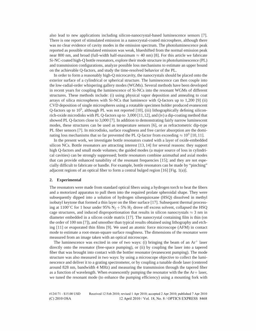
Wavelength (nm)780 800 820 840 860
TM
Pho
tolu
min
esce
nce
(arb
. uni
ts)
780 800 820 840 860Wavelength (nm)
TE12345678
c)12345678
d)
a)b)
8 7 6 5 4 3 2 1
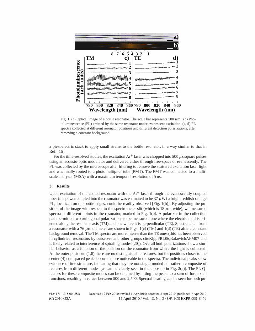
Fig. 1. (a) Optical image of a bottle resonator. The scale bar represents 100 μm . (b) Pho-toluminescence (PL) emitted by the same resonator under evanescent excitation. (c, d) PLspectra collected at different resonator positions and different detection polarizations, afterremoving a constant background.
a piezoelectric stack to apply small strains to the bottle resonator, in a way similar to that inRef. [15].
For the time-resolved studies, the excitation Ar+ laser was chopped into 500 μs square pulsesusing an acousto-optic modulator and delivered either through free-space or evanescently. ThePL was collected by the microscope after filtering to remove the scattered excitation laser lightand was finally routed to a photomultiplier tube (PMT). The PMT was connected to a multi-scale analyzer (MSA) with a maximum temporal resolution of 5 ns.
3. Results
Upon excitation of the coated resonator with the Ar+ laser through the evanescently coupledfiber (the power coupled into the resonator was estimated to be 37 μW) a bright reddish-orangePL, localized on the bottle edges, could be readily observed [Fig. 1(b)]. By adjusting the po-sition of the image with respect to the spectrometer slit (which is 18 μm wide), we measuredspectra at different points in the resonator, marked in Fig. 1(b). A polarizer in the collectionpath permitted two orthogonal polarizations to be measured: one where the electric field is ori-ented along the resonator axis (TM) and one where it is perpendicular (TE). Spectra taken froma resonator with a 76 μm diameter are shown in Figs. 1(c) (TM) and 1(d) (TE) after a constantbackground removal. The TM spectra are more intense than the TE ones (this has been observedin cylindrical resonators by ourselves and other groups citeKippPRL06,RakovichAFM07 andis likely related to interference of spiraling modes [20]). Overall both polarizations show a sim-ilar behavior as a function of the position on the resonator from where the light is collected:At the outer positions (1,8) there are no distinguishable features, but for positions closer to thecenter (4) equispaced peaks become more noticeable in the spectra. The individual peaks showevidence of fine structure, indicating that they are not single-moded but rather a composite offeatures from different modes [as can be clearly seen in the close-up in Fig. 2(a)]. The PL Q-factors for these composite modes can be obtained by fitting the peaks to a sum of lorentzianfunctions, resulting in values between 500 and 2,500. Spectral beating can be seen for both po-
#124171 - $15.00 USD Received 12 Feb 2010; revised 1 Apr 2010; accepted 2 Apr 2010; published 7 Apr 2010(C) 2010 OSA 12 April 2010 / Vol. 18, No. 8 / OPTICS EXPRESS 8469
827.96 827.98 828 828.02 828.04 828.0600.20.40.60.8
1T
rans
mis
sion
828.066 828.067 828.068 828.069 828.07Wavelength (nm)
00.20.40.60.8
1
Tra
nsm
issi
on825 826 827 828 829 830 PL
(ar
b. u
nits
)
00.20.40.60.8
1
Tra
nsm
issi
on
b)
c)
a)
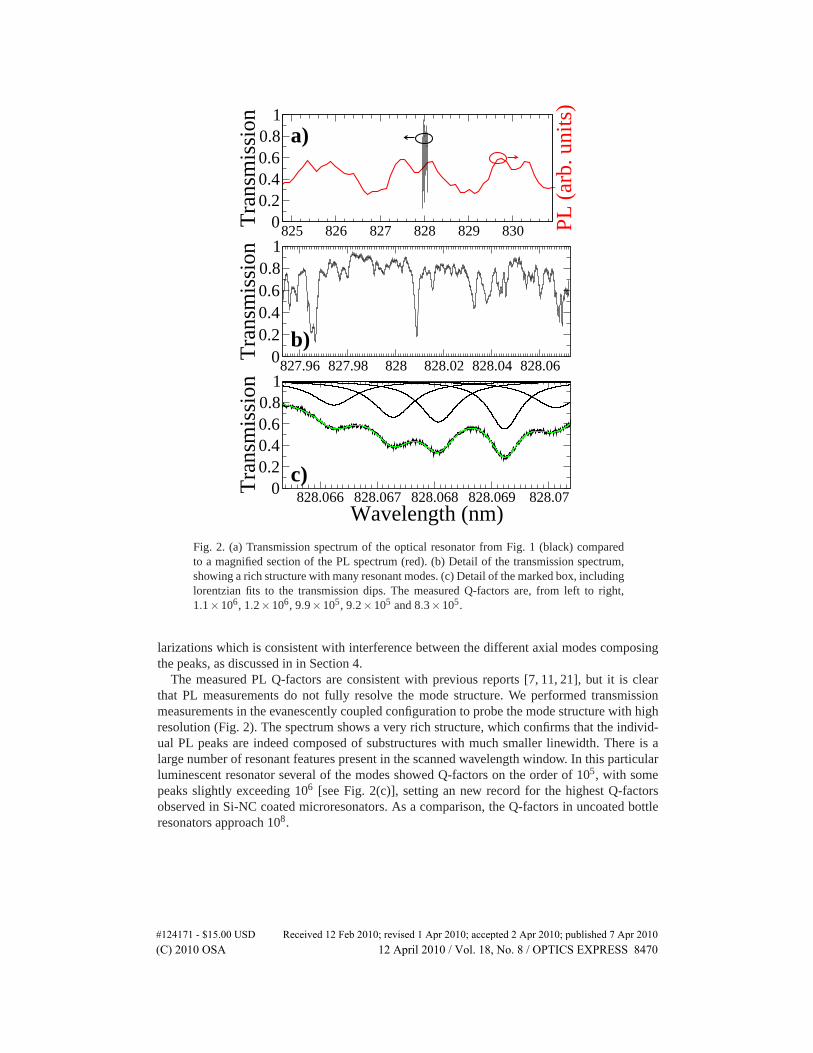
Fig. 2. (a) Transmission spectrum of the optical resonator from Fig. 1 (black) comparedto a magnified section of the PL spectrum (red). (b) Detail of the transmission spectrum,showing a rich structure with many resonant modes. (c) Detail of the marked box, includinglorentzian fits to the transmission dips. The measured Q-factors are, from left to right,1.1×106, 1.2×10⁶, 9.9×10⁵, 9.2×10⁵ and 8.3×10⁵.
larizations which is consistent with interference between the different axial modes composingthe peaks, as discussed in in Section 4.
The measured PL Q-factors are consistent with previous reports [7, 11, 21], but it is clearthat PL measurements do not fully resolve the mode structure. We performed transmissionmeasurements in the evanescently coupled configuration to probe the mode structure with highresolution (Fig. 2). The spectrum shows a very rich structure, which confirms that the individ-ual PL peaks are indeed composed of substructures with much smaller linewidth. There is alarge number of resonant features present in the scanned wavelength window. In this particularluminescent resonator several of the modes showed Q-factors on the order of 105, with somepeaks slightly exceeding 106 [see Fig. 2(c)], setting an new record for the highest Q-factorsobserved in Si-NC coated microresonators. As a comparison, the Q-factors in uncoated bottleresonators approach 108.
#124171 - $15.00 USD Received 12 Feb 2010; revised 1 Apr 2010; accepted 2 Apr 2010; published 7 Apr 2010(C) 2010 OSA 12 April 2010 / Vol. 18, No. 8 / OPTICS EXPRESS 8470
z
425,1
425,2 417,2
417,1b)
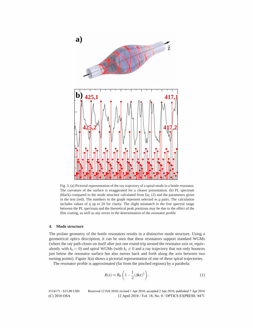
a)
Fig. 3. (a) Pictorial representation of the ray trajectory of a spiral mode in a bottle resonator.The curvature of the surface is exaggerated for a clearer presentation. (b) PL spectrum(black) compared to the mode structure calculated from Eq. (2) and the parameters givenin the text (red). The numbers in the graph represent selected m,q pairs. The calculationincludes values of q up to 20 for clarity. The slight mismatch in the free spectral rangebetween the PL spectrum and the theoretical peak positions may be due to the effect of thefilm coating, as well as any errors in the determination of the resonator profile
4. Mode structure
The prolate geometry of the bottle resonators results in a distinctive mode structure. Using ageometrical optics description, it can be seen that these resonators support standard WGMs(where the ray path closes on itself after just one round-trip around the resonator axis or, equiv-alently with kz = 0) and spiral WGMs (with kz �= 0 and a ray trajectory that not only bouncesjust below the resonator surface but also moves back and forth along the axis between twoturning points). Figure 3(a) shows a pictorial representation of one of these spiral trajectories.
The resonator profile is approximated (far from the pinched regions) by a parabola:
R(z) ≈ R0
(1− 1
2(Δkz)2
), (1)
#124171 - $15.00 USD Received 12 Feb 2010; revised 1 Apr 2010; accepted 2 Apr 2010; published 7 Apr 2010(C) 2010 OSA 12 April 2010 / Vol. 18, No. 8 / OPTICS EXPRESS 8471
where R0 = 38.1μm is the maximum radius (where is arbitrarily located at z = 0) and Δk =0.002μm −1 is the profile curvature. These values were obtained by capturing an image usingan optical microscope and a color charge-coupled-device (CCD) camera, tracing the resonatorprofile from the image and fitting Eq. (1) to the trace.
Due to the optical confinement on the resonator boundary, there is a discrete set of allowedeigenmodes [22], with wavenumbers
k2mq =
m2
R20
+(q+12)ΔEm, (2)
where m is the usual azimuthal order number (corresponding to the number of nodes in thefield along the azimuthal direction), q is an axial order number representing the number ofnodes along the resonator axis and ΔE = 2mΔk/R0 (only the lowest radial mode is consideredin the analysis, so there is no radial order number). The axial number q will also influence thez positions of the peak field since there are two symmetric positions, the caustics, on the axiswhere the field peaks: the larger q is, these peaks will be farther away from the center.
Using these equation with n = 1.453 for silica at room temperature, we can quantify themode spacings (while the model does not account for the thin nanocrystal film, we can assumethat the latter will cause a minor red shift of the mode resonant wavelengths [23]). For example,there is an upper limit of m = 420 for the mode wavelengths to fall within the scanned range(827.95-828.07 nm). The spacing between two modes with the same q number and consecutivem numbers is Δνm ≈ c/2πnR0 ≈ 862 GHz ≈ 2 nm, as can be appreciated in Fig. 2(a). Thespacing between two modes with the same m number but consecutive q numbers, would thenbe Δνq ≈ cΔk/2π ≈ 95 MHz ≈ 0.2 nm, which is larger than the scanned range of approximately0.11 nm. Thus we can safely infer that the multitude of modes observed in the transmissionspectrum in Fig. 2(b) possess different m and q numbers. Since the tapered fiber was locatedclose to the center of the resonator, modes with lower q numbers will be more efficiently excitedso the measured modes should have values near the upper limit in m. A comparison showingqualitative agreement between the calculated spectra and the measured PL at a given positionis given in Fig. 3(b).
The eigenmode distribution from Eq. (2) also explains why the resonant peaks in Fig. 1seem to shift when measured at different axial positions. Mode PL emission will be strongest atthe caustics, so the higher q numbers imply that the strongest emission will be located fartheraway from the resonator midpoint. As we collect emission from locations away from the cen-ter, the predominant PL comes from modes with higher q values (and lower m values) whichwill certainly show a different resonant wavelength. This also provides an explanation for thefine structure observed in Fig. 2(a), as the spectrometer slit (1.8 μm accounting for the 10Xmagnification of the microscope) collects emission from modes with different values for q.
5. Loss mechanisms
The addition of the coating decreases the Q-factor in the resonators by one or two orders ofmagnitude. The ability to maintain high Q-factors in coated resonators matters in differentcontexts: it is critical to minimize the threshold in a laser and it enhances the interaction betweenlight and matter in a way that could make cavity phenomena like the Purcell effect or strongcoupling easier to achieve. It is also important for low-power operation of resonator-basedoptical filters. We can analyze the contribution of different loss mechanisms to the degradationof Q-factors to see if it would be possible in principle to improve them still further. The mainloss mechanisms in Si-NC-containing resonators when the excitation power is kept low and thewavelength is in the near-infrared range are radiation losses in the modes, surface roughnessscattering, Mie scattering and inter-band absorption by the nanocrystals [11]. The final Q-factor
#124171 - $15.00 USD Received 12 Feb 2010; revised 1 Apr 2010; accepted 2 Apr 2010; published 7 Apr 2010(C) 2010 OSA 12 April 2010 / Vol. 18, No. 8 / OPTICS EXPRESS 8472
is then given byQ−1
f = Q−1Rad +Q−1
Rough +Q−1Mie +Q−1
IB . (3)
When the resonator is excited by the blue light emitted by the Ar+ laser, a population of car-riers builds up in the Si-NCs. These excited carriers can absorb the light circulating within thecavity [24], and thus introduce a new loss channel. This additional loss mechanism is normallycalled confined-carrier-absorption (CCA), and we will consider it separately.
In all the following calculations, we have used the modal properties (field profile, effectiveindex, confinement factor) calculated for a coated cylindrical resonator [7], which should besimilar to those of modes which don’t travel far from the center of the bottle resonator.
5.1. Radiation loss
Since we have measured Q-factors close to 108 in uncoated cavities, we can assume QRad ≥ 108,and the loss due to radiation is negligible. This is not surprising, given the relatively largediameter of 76 μm .
5.2. Surface roughness
We can estimate the loss coefficient due to scattering from the roughness at the surface adaptingthe result from Ref. [25] for the case of a whispering gallery mode, approximating the fielddistribution and effective index by those calculated for a coated cylinder [7]:
αRough = ϕ2(r)(n2film −1)
k20
8nfilmσ2
√π
neff2−1, (4)
where ϕ(r) is the field distribution at the resonator surface, with the normalization∫ ∞0 ϕ2(r)dr = 1, nfilm = 1.68 [26] is the refractive index of the nanocrystal film, neff = 1.41
is the effective refractive index of the whispering gallery mode, k0 = 2π/λ is the vacuum wavevector and σ = 3.40 nm is the AFM-measured root-mean-square roughness of the surface. Wetake the wavelength to be λ = 829.9 nm.
Using these numbers in Eq. (4), we obtain αRough = 0.05 cm−1, and from that we estimateQRough as follows:
QRough =2πneff
λαRough= 2.1×10⁶. (5)
5.3. Inter-band absorption
The estimated losses caused by inter-band absorption by Si-NC can be estimated by followingthe procedure outlined in Ref. [11] from the absorption cross-section, the nanocrystal size dis-tribution and the mode field profile. We obtained the nanocrystal size distribution ρ(R) fromenergy-filtered transmission electron microscopy (see the appendix for details). Then, the ab-sorption is given by [11]
αIB = Γ(λ )∫ R=Rmax
R=R(λ )σabs(R)ρ(R)dR, (6)
where σabs(R) is the absorption cross-section (as a function of the nanocrystal radius), R(λ )is the radius for a nanocrystal with an emission of wavelength λ and Rmax is the radius of thelargest nanocrystal in the sample and Γ(λ ) ≈ 0.01 is the confinement factor calculated fromthe mode profile. Using the values reported in Ref. [27], we find αIB = 2.24×10⁻³ cm−1 andQIB = 4.7×10⁷.
#124171 - $15.00 USD Received 12 Feb 2010; revised 1 Apr 2010; accepted 2 Apr 2010; published 7 Apr 2010(C) 2010 OSA 12 April 2010 / Vol. 18, No. 8 / OPTICS EXPRESS 8473
5.4. Mie scattering
Finally, the Mie scattering losses can be estimated by adding the contribution for each nanocrys-tal size weighted by the size distribution,
αMie = Γ(λ )∫ R=Rmax
R=Rmin
σMie(R,λ )ρ(R)dR, (7)
with the scattering cross-section given by the Rayleigh formula [28]
σMie =8π3
(2πnSiO2
λ
)4
R6
(n2
Si −n2SiO2
n2Si +2n2
SiO2
)2
. (8)
Taking nSiO2 = 1.46 and nSi = 3.69, we find σMie = 9.25×10⁻⁴ cm−1 and QMie = 1.2×10⁸.The final estimated Q-factor results Qf = 1.9×10⁶, comparable to what we observed in the
transmission spectra. From this analysis, surface roughness scattering is the dominant loss fac-tor, followed by interband absorption. Mie scattering does not seem to contribute significantlyto the scattering, just like radiation losses. The films produced by the dip-coating method are al-ready very smooth (as compared, for instance, to lithographically fabricated microdisks whichhave a much higher root-mean-square roughness [11] or evaporated thin films. However, theexperimental Q-factors could be increased (up to a factor of 6) by further improving their sur-face properties. It is worthwhile to note that Mie scattering and interband absorption are greatlyreduced because of the thinness of the nanocrystal-containing film (expressed by the small con-finement factor Γ). Thicker films would increase the losses due to these intrinsic mechanisms,and correspondingly decrease the maximum achievable Q-factors. Our fabrication method thenbecomes attractive for applications requiring resonators with high Q-factors.
5.5. Confined carrier absorption
To estimate the degree of confined carrier absorption, we measured the linewidth of a resonantmode under free-space excitation of the resonator with the Ar+ laser. Then, comparing thislinewidth with the one in the absence of an external excitation we can obtain an estimate of theextra loss induced by the free carrier absorption. At an excitation intensity of 34 kW/cm2 (themaximum we could safely route through our microscope), the linewidth increased by 0.42 pm.Following Ref. [24], this results in αCCA = 2πneff/(λ 2Γ) = 0.054 cm−1 and QCCA = 2.0×10⁶.Combined with the near-infrared Q-factor calculated above, the Ar+-excited Q-factor would be
QAr+ = (Qf +QCCA)−1 = 9.7×10⁵. (9)
The evolution of the transmission spectra as the pump power increases [Fig. 4(a)] shows thegradual increase in the full-width half-maximum (FWHM) of the modes as the pump intensityincreases. There is also a red-shift associated with the pumping, which is due to thermal effectson the resonator (we verified this by corroborating that the time scale of the shift is in the orderof a tens of milliseconds). Figure 4(b) displays the fitted mode FWHM as a function of incidentpower. At the lower intensities the mode linewidth stays roughly constant while it increasesfor pump intensities larger than 19 kW/cm2, the point where the confined carrier absorptionbecomes the dominant loss mechanism.
5.6. Losses and PL linewidth
The previous analysis established Q-factors in the order of 106 taking into account different lossmechanisms that apply to resonators coated with a thin film containing Si-NCs. However, the Q-factors measured in the PL are much lower (between 500 to 2,500). These values are not limited
#124171 - $15.00 USD Received 12 Feb 2010; revised 1 Apr 2010; accepted 2 Apr 2010; published 7 Apr 2010(C) 2010 OSA 12 April 2010 / Vol. 18, No. 8 / OPTICS EXPRESS 8474
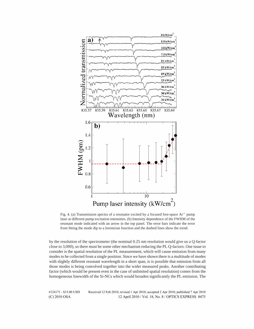
Fig. 4. (a) Transmission spectra of a resonator excited by a focused free-space Ar+ pumplaser at different pump excitation intensities. (b) Intensity dependence of the FWHM of theresonant mode indicated with an arrow in the top panel. The error bars indicate the errorfrom fitting the mode dip to a lorentzian function and the dashed lines show the trend.
by the resolution of the spectrometer (the nominal 0.25 nm resolution would give us a Q-factorclose to 3,000), so there must be some other mechanism reducing the PL Q-factors. One issue toconsider is the spatial resolution of the PL measurement, which will cause emission from manymodes to be collected from a single position. Since we have shown there is a multitude of modeswith slightly different resonant wavelength in a short span, is is possible that emission from allthose modes is being convolved together into the wider measured peaks. Another contributingfactor (which would be present even in the case of unlimited spatial resolution) comes from thehomogeneous linewidth of the Si-NCs which would broaden significantly the PL emission. The
#124171 - $15.00 USD Received 12 Feb 2010; revised 1 Apr 2010; accepted 2 Apr 2010; published 7 Apr 2010(C) 2010 OSA 12 April 2010 / Vol. 18, No. 8 / OPTICS EXPRESS 8475
detailed theroy about this broadening mechanism, arising from a full integration and theoreticalanalysis of Fermi’s Golden Rule for coupled quantum dot-cavity systems, will be published ina separate paper [29].
6. High-power excitation
Steady-state spectral measurements at increasing pump powers (up to an estimated 380 μWtransferred from the waveguide into the resonator, corresponding to 9 mW of circulating powerfor a Q-factor of 105) did not show qualitative changes beyond an increase in PL intensity (inparticular, there was no clear trend of an increasing PL linewidth as the pump power increased).The upper inset in Fig. 5 shows a representative spectrum, together with ones from the free-space configuration and a flat film. The WGMs are not observable in this spectra because lightwas collected from the whole resonator so as not to miss possible lasing modes. The free-space-excited resonator PL peak was blue shifted compared to that from the flat film, whilethe evanescently excited PL no longer had a well defined peak, instead gradually rising intothe blue part of the spectrum and was eventually cut off by the longpass filter that blocked thelaser. This blue shift is consistent with the high excitation power density inside the resonators,especially for evanescent pumping, which increases the contribution of fast processes.
7. Time-resolved behavior
Since there have been reports of short-lived gain in Si-NCs [30], we also performed time-resolved studies of the PL. As a baseline, we measured the time-resolved PL from a flat filmof oxide-embedded Si-NCs (Fig. 5). This showed a typical stretched exponential decay, I(t) =I(0)exp(−( t
τ )β ) with τ = 21 μs and β = 0.77. The emission from a coated resonator using free-space excitation gave a similar curve (τ = 16 μs, β = 0.55). The trace from the evanescentlyexcited resonator showed a fast rise (rise time ≈ 200 ns, close to the AOM modulator limit)followed by a slower decay to a steady state. The decay of this steady state was also on theorder of 200 ns and was followed by a much weaker decay with a time constant on the order ofmicroseconds.
The lifetime decreases and the spectrum blueshifts on going from a flat film to a free-space-pumped cavity and finally to an evanescently pumped cavity (Fig. 5). In fact, the evanescentlycoupled resonator is somewhat reminiscent of the gain reported in Si-NCs [30] but with a muchlonger decay to the steady state, which is inconsistent with Auger-induced gain quenching [6].No spectral narrowing or threshold behavior was observed when changing the pump power (seethe lower inset of Fig. 5), only saturation at high pump powers. The fast (nanosecond) compo-nent of the rise and decay times are consistent with the so-called F-band emission [31], likelydue to luminescent defects in silicon-rich oxide [32] which are not saturated in the evanescently-pumped configuration (the nanocrystals themselves contributing only to the low-amplitude slowdynamics). The initial decay to a steady state just after the pulse onset was unexpected, and itmay be due to a reversible photobleaching of luminescent centers caused by the high excitationpower density coupled into the cavity. It was only observed for evanescent pumping. Despite thesmall time constants and bluer emission, the lack of sharp peaks in the spectrum coupled withthe absence of a threshold behavior leads us to conclude the Si-NCs do not show stimulatedemission in these excitation and measurement configurations.
8. Conclusion
In summary, we studied Si-NC-coated bottle resonators under evanescent excitation. The tun-ing range and high Q- factors of bottle resonators allow for efficient pumping of the Si-NCs,leading to the emission of luminescence coupled to resonator modes. The PL modes approach
#124171 - $15.00 USD Received 12 Feb 2010; revised 1 Apr 2010; accepted 2 Apr 2010; published 7 Apr 2010(C) 2010 OSA 12 April 2010 / Vol. 18, No. 8 / OPTICS EXPRESS 8476
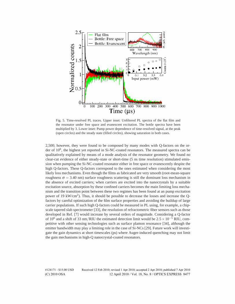
Fig. 5. Time-resolved PL traces. Upper inset: Unfiltered PL spectra of the flat film andthe resonator under free space and evanescent excitation. The bottle spectra have beenmultiplied by 3. Lower inset: Pump power dependence of time-resolved signal, at the peak(open circles) and the steady state (filled circles), showing saturation in both cases.
2,500; however, they were found to be composed by many modes with Q-factors on the or-der of 106, the highest yet reported in Si-NC-coated resonators. The measured spectra can bequalitatively explained by means of a mode analysis of the resonator geometry. We found noclear-cut evidence of either steady-state or short-time (5 ns time resolution) stimulated emis-sion when pumping the Si-NC-coated resonator either in free space or evanescently despite thehigh Q-factors. These Q-factors correspond to the ones estimated when considering the mostlikely loss mechanisms. Even though the films as fabricated are very smooth (root-mean-squareroughness σ = 3.40 nm) surface roughness scattering is still the dominant loss mechanism inthe absence of excited carriers; when carriers are excited into the nanocrystals by a suitableexcitation source, absorption by these confined carriers becomes the main limiting loss mecha-nism and the transition point between these two regimes has been found at an pump excitationpower of 19 kW/cm2). Thus, it should be possible to decrease the losses and increase the Q-factors by careful optimization of the film surface properties and avoiding the buildup of largecarrier populations. If such high Q-factors could be measured in PL using, for example, a chip-scale tapered slab spectrometer [33], the resolution of refractometric fiber sensors such as thosedeveloped in Ref. [7] would increase by several orders of magnitude. Considering a Q-factorof 106 and a shift of 33 nm/RIU the estimated detection limit would be 2.5×10⁻⁵ RIU, com-petitive with other sensing technologies such as surface plamon resonance [34], although theemitter bandwidth may play a limiting role in the case of Si-NCs [29]. Future work will investi-gate the gain dynamics at short timescales (ps) where Auger-induced quenching may not limitthe gain mechanisms in high-Q nanocrystal-coated resonators.
#124171 - $15.00 USD Received 12 Feb 2010; revised 1 Apr 2010; accepted 2 Apr 2010; published 7 Apr 2010(C) 2010 OSA 12 April 2010 / Vol. 18, No. 8 / OPTICS EXPRESS 8477
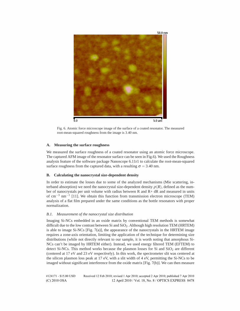
Fig. 6. Atomic force microscope image of the surface of a coated resonator. The measuredroot-mean-squared roughness from the image is 3.40 nm.
A. Measuring the surface roughness
We measured the surface roughness of a coated resonator using an atomic force microscope.The captured AFM image of the resonator surface can be seen in Fig.6). We used the Roughnessanalysis feature of the software package Nanoscope 6.11r1 to calculate the root-mean-squaredsurface roughness from the captured data, with a resulting σ = 3.40 nm.
B. Calculating the nanocrystal size-dependent density
In order to estimate the losses due to some of the analyzed mechanisms (Mie scattering, in-terband absorption) we need the nanocrystal size-dependent density ρ(R), defined as the num-ber of nanocrystals per unit volume with radius between R and R+ dR and measured in unitsof cm−3 nm−1 [11]. We obtain this function from transmission electron microscope (TEM)analysis of a flat film prepared under the same conditions as the bottle resonators with propernormalization.
B.1. Measurement of the nanocrystal size distribution
Imaging Si-NCs embedded in an oxide matrix by conventional TEM methods is somewhatdifficult due to the low contrast between Si and SiO2. Although high resolution TEM (HRTEM)is able to image Si-NCs [Fig. 7(a)], the appearance of the nanocrystals in the HRTEM imagerequires a zone-axis orientation, limiting the application of the technique for determining sizedistributions (while not directly relevant to our sample, it is worth noting that amorphous Si-NCs can’t be imaged by HRTEM either). Instead, we used energy filtered TEM (EFTEM) todetect Si-NCs. This method works because the plasmon losses for Si and SiO2 are different(centered at 17 eV and 23 eV respectively). In this work, the spectrometer slit was centered atthe silicon plasmon loss peak at 17 eV, with a slit width of 4 eV, permitting the Si-NCs to beimaged without significant interference from the oxide matrix [Fig. 7(b)]. We can then measure
#124171 - $15.00 USD Received 12 Feb 2010; revised 1 Apr 2010; accepted 2 Apr 2010; published 7 Apr 2010(C) 2010 OSA 12 April 2010 / Vol. 18, No. 8 / OPTICS EXPRESS 8478
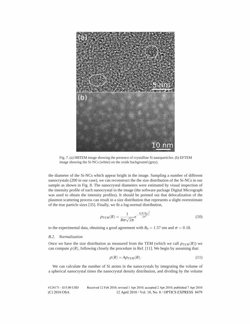
Fig. 7. (a) HRTEM image showing the presence of crystalline Si nanoparticles. (b) EFTEMimage showing the Si-NCs (white) on the oxide background (grey).
the diameter of the Si-NCs which appear bright in the image. Sampling a number of differentnanocrystals (200 in our case), we can reconstruct the the size distribution of the Si-NCs in oursample as shown in Fig. 8. The nanocrystal diameters were estimated by visual inspection ofthe intensity profile of each nanocrystal in the image (the software package Digital Micrographwas used to obtain the intensity profiles). It should be pointed out that delocalization of theplasmon scattering process can result in a size distribution that represents a slight overestimateof the true particle sizes [35]. Finally, we fit a log-normal distribution,
ρTEM(R) =1
Rσ√
2πe− ln(R/R0)2
2σ2 (10)
to the experimental data, obtaining a good agreement with R0 = 1.57 nm and σ = 0.18.
B.2. Normalization
Once we have the size distribution as measured from the TEM (which we call ρTEM(R)) wecan compute ρ(R), following closely the procedure in Ref. [11]. We begin by assuming that:
ρ(R) = AρTEM(R). (11)
We can calculate the number of Si atoms in the nanocrystals by integrating the volume ofa spherical nanocrystal times the nanocrystal density distribution, and dividing by the volume
#124171 - $15.00 USD Received 12 Feb 2010; revised 1 Apr 2010; accepted 2 Apr 2010; published 7 Apr 2010(C) 2010 OSA 12 April 2010 / Vol. 18, No. 8 / OPTICS EXPRESS 8479
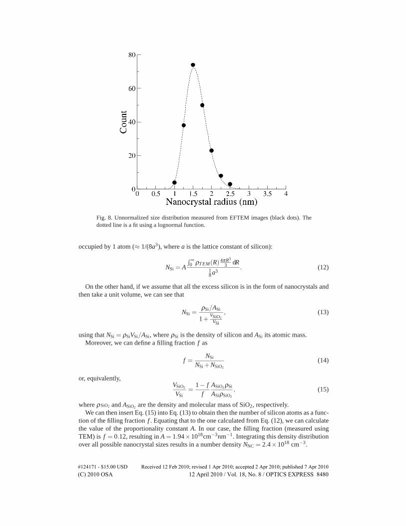
Fig. 8. Unnormalized size distribution measured from EFTEM images (black dots). Thedotted line is a fit using a lognormal function.
occupied by 1 atom (≈ 1/(8a3), where a is the lattice constant of silicon):
NSi = A
∫ ∞0 ρTEM(R) 4πR3
3 dR18 a3
. (12)
On the other hand, if we assume that all the excess silicon is in the form of nanocrystals andthen take a unit volume, we can see that
NSi =ρSi/ASi
1+VSiO2VSi
, (13)
using that NSi = ρSiVSi/ASi, where ρSi is the density of silicon and ASi its atomic mass.Moreover, we can define a filling fraction f as
f =NSi
NSi +NSiO2
(14)
or, equivalently,VSiO2
VSi=
1− ff
ASiO2 ρSi
ASiρSiO2
, (15)
where ρSiO2 and ASiO2 are the density and molecular mass of SiO2, respectively.We can then insert Eq. (15) into Eq. (13) to obtain then the number of silicon atoms as a func-
tion of the filling fraction f . Equating that to the one calculated from Eq. (12), we can calculatethe value of the proportionality constant A. In our case, the filling fraction (measured usingTEM) is f = 0.12, resulting in A = 1.94×1018cm−3nm−1. Integrating this density distributionover all possible nanocrystal sizes results in a number density NNC = 2.4×1018 cm−3.
#124171 - $15.00 USD Received 12 Feb 2010; revised 1 Apr 2010; accepted 2 Apr 2010; published 7 Apr 2010(C) 2010 OSA 12 April 2010 / Vol. 18, No. 8 / OPTICS EXPRESS 8480
Acknowledgements
The authors would like to acknowledge financial support by NSERC, iCORE andCIPI. The transmission electron microscopy was done at the National Institute for Nan-otechnology Electron Microscopy Facility. The peak fitting was done using Fityk 0.8.8(http://fityk.sourceforge.net). The pictorial representation of a resonator in Fig. 3(a) was drawnby M. Wilson. We would also like to acknowledge M. Sumetsky, who in a 2004 paper intro-duced theoretically the concept of whispering-gallery bottle resonators.
#124171 - $15.00 USD Received 12 Feb 2010; revised 1 Apr 2010; accepted 2 Apr 2010; published 7 Apr 2010(C) 2010 OSA 12 April 2010 / Vol. 18, No. 8 / OPTICS EXPRESS 8481
Copyright © 2022 FDOKUMEN