signal electronics for embedded and intelligent sensor systems
214
TOWARDS DYNAMICALLY RECONFIGURABLE MIXED- SIGNAL ELECTRONICS FOR EMBEDDED AND INTELLIGENT SENSOR SYSTEMS Beiträge zur Entwicklung dynamisch rekonfigurierbarer, gemischt analog- digitaler Elektronik für eingebettete und intelligente Sensorsysteme vom Fachbereich Elektrotechnik und Informationstechnik der Technischen Universität Kaiserslautern zur Erlangung des akademischen Grades eines Doktor der Ingenieurwissenschaften (Dr.-Ing.) Dissertation von Senthil Kumar Lakshmanan geb. in Tiruchy (Indien) D 386 Eingereicht am: 25. June 2008 Tag der mündlichen Prüfung: 04. November 2008 Dekan des Fachbereichs: Prof. Dr.-Ing. Steven Liu Promotionskommission Vorsitzender: Prof. Dr.-Ing. Remigius Zengerle Berichterstattende: Prof. Dr.-Ing. Andreas König Prof. Dr.-Ing. Ulrich Rückert
-
Upload
khangminh22 -
Category
Documents
-
view
0 -
download
0
Transcript of signal electronics for embedded and intelligent sensor systems

TOWARDS DYNAMICALLY RECONFIGURABLE MIXED-SIGNAL ELECTRONICS FOR EMBEDDED AND
INTELLIGENT SENSOR SYSTEMS
Beiträge zur Entwicklung dynamisch rekonfigurierbarer, gemischt analog-digitaler Elektronik für eingebettete und intelligente Sensorsysteme
vom
Fachbereich Elektrotechnik und Informationstechnik der Technischen Universität Kaiserslautern
zur Erlangung des akademischen Grades eines
Doktor der Ingenieurwissenschaften (Dr.-Ing.)
Dissertation
von
Senthil Kumar Lakshmanan geb. in Tiruchy (Indien)
D 386
Eingereicht am: 25. June 2008
Tag der mündlichen Prüfung: 04. November 2008
Dekan des Fachbereichs: Prof. Dr.-Ing. Steven Liu
Promotionskommission
Vorsitzender: Prof. Dr.-Ing. Remigius Zengerle
Berichterstattende: Prof. Dr.-Ing. Andreas König
Prof. Dr.-Ing. Ulrich Rückert


© Copyright by Senthil Kumar Lakshmanan, 2008
All Rights Reserved

II
II
Erklärung
Hiermit versichere ich, dass ich die vorliegende Arbeit selbst angefertigt und verfasst habe und alle benutzen Hilfsmittel in der Arbeit angegeben habe. Die vorliegende Dissertation oder Teile hiervon würden noch nicht als Prüfungsarbeit für eine staatliche oder andere wissenschaftliche Prüfung eingereicht.
Kaiserslautern, den 25/06/08
M.Sc. Senthil Kumar Lakshmanan

I
Abstract
Rapid growth in sensors and sensor technology introduces variety of products to the market. The increasing number of available sensor concepts and implementations demands more versatile sensor electronics and signal conditioning. Nowadays signal conditioning for the available spectrum of sensors is becoming more and more challenging. Moreover, developing a sensor signal conditioning ASIC is a function of cost, area, and robustness to maintain signal integrity. Field programmable analog approaches and the recent evolvable hardware approaches offer partial solution for advanced compensation as well as for rapid prototyping.
The recent research field of evolutionary concepts focuses predominantly on digital and is at its advancement stage in analog domain. Thus, the main research goal is to combine the ever increasing industrial demand for sensor signal conditioning with evolutionary concepts and dynamically reconfigurable matched analog arrays implemented in main stream Complementary Metal Oxide Semiconductors (CMOS) technologies to yield an intelligent and smart sensor system with acceptable fault tolerance and the so called self-x features, such as self-monitoring, self-repairing and self-trimming. The conceptual illustration of the aspired research work is depicted in Figure Ab-1.
Figure Ab-1: Symbolic representation of the research work
For this aim, the work suggests and progresses towards a novel, time continuous and dynamically reconfigurable signal conditioning hardware platform suitable to support variety of sensors.
The state-of-the-art has been investigated with regard to existing programmable/reconfigurable analog devices and the common industrial application scenario and circuits, in particular including resource and sizing analysis for proper motivation of design decisions. The pursued intermediate granular level approach called as Field Programmable Medium-granular mixed signal Array (FPMA) offers flexibility, trimming and rapid prototyping capabilities. The proposed approach targets at the investigation of industrial applicability of evolvable hardware concepts and to merge it with reconfigurable or programmable analog concepts, and industrial electronics standards and needs for next generation robust and flexible sensor systems. The devised programmable sensor signal conditioning test chips, namely FPMA1/FPMA2, designed in 0.35 µm (C35B4) Austriamicrosystems, can be used as a single instance, off the shelf chip at the PCB level for

II
II
conditioning or in the loop with dedicated software to inherit the aspired self-x features. The use of such self–x sensor system carries the promise of improved flexibility, better accuracy and reduced vulnerability to manufacturing deviations and drift. An embedded system, namely PHYTEC miniMODUL-515C was used to program and characterize the mixed-signal test chips in various feedback arrangements to answer some of the questions raised by the research goals.
Wide range of established analog circuits, ranging from single output to fully differential amplifiers, was investigated at different hierarchical levels to realize circuits like instrumentation amplifier and filters. A more extensive design issues based on low-power like for e.g., sub-threshold design were investigated and a novel soft sleep mode idea was proposed. The bandwidth limitations observed in the state of the art fine granular approaches were enhanced by the proposed intermediate granular approach. The so designed sensor signal conditioning instrumentation amplifier was then compared to the commercially available products in the market like LT 1167, INA 125 and AD 8250.
In an adaptive prototype, evolutionary approaches, in particular based on particle swarm optimization with multi-objectives, were just deployed to all the test samples of FPMA1/FMPA2 (15 each) to exhibit self-x properties and to recover from manufacturing variations and drift. The variations observed in the performance of the test samples were compensated through reconfiguration for the desired specification.

III
Acknowledgments
First and foremost, I wish to express my gratitude and sincere thanks to my advisor Prof. Dr.-Ing. Andreas König for the suggestions on the research topic. I am deeply indebted to him for his advice, suggestions, and numerous discussions on my research and help throughout my stay. I would like to thank my second reporter Prof. Dr-Ing. Ulrich Rückert for his interest in my work.
I would also like to acknowledge PHYTEC Messtechnik GmbH, Mainz for funding the chips manufacturing which are used in the scope of this thesis work.
I also take this opportunity to thank the system administrators Mr. Markus Müller and Mr. Andreas Christmann. I thank Dr. Peter Tawdross for employing optimization techniques on to the chips designed in this thesis work. I am thankful to Mr. Thomas Gräf for designing PCB test plugs. I am thankful to Mr. Robert Freier and Mr. Jürgen Hornberger for helping me in german language translations of the abstract.
Above all I would like to thank my parents Vijayalakshmi, L and Lakshmanan, R for their support, encouragement and patience. Last but not least, I would also like to thank my relatives and friends for their constant motivation.

IV
IV
To my mother
- Vijayalakshmi. L

V
Contents 1. Introduction...............................................................................................................................10
1.1 Signal Conditioning in Integrated Smart Sensor System .................................................. 10 1.1.1 Trimming / Calibration Techniques....................................................................... 11
1.2 Motivation of this thesis .................................................................................................... 13 1.3 Aims of this thesis ............................................................................................................. 14 1.4 Organization of the Thesis................................................................................................. 15
2. State – of – the– Art of Programmable / Reconfigurable CMOS Analog Electronics.........16 2.1 Introduction ....................................................................................................................... 16 2.2 Overview of Commercial Programmable Analog / Mixed-Signal IC’s............................ 19
2.2.1 IMP- Electrically Programmable Analog Devices (EPAC)................................... 19 2.2.2 Motorola MPAA020 .............................................................................................. 19 2.2.3 Zetex Totally Reconfigurable Analog Circuit ....................................................... 20 2.2.4 Anadigm AN231E04 Dynamical Reconfigurable dpASP..................................... 21 2.2.5 Texas Instruments – PGA- Digital Trim for Non-Linearity’s ............................... 23 2.2.6 Analog Devices – Digi Trim AD855x series ......................................................... 23 2.2.7 Lattice ispPAC ....................................................................................................... 25 2.2.8 Cypress PSoC......................................................................................................... 25 2.2.9 Analog Linear Devices – EPAD ............................................................................ 27 2.2.10 Melexis – Programmable sensor interface MLX90308 ......................................... 27 2.2.11 MaZeT – Programmable Gain Transimpedance amplifier MTI04Bx-BF............. 27 2.2.12 Embedded and Programmable Sensor Calibration. ............................................... 28
2.3 Overview of Academic Reprogrammable Analog Hardware ........................................... 30 2.3.1 FPAA - University of Toronto (Gulak).................................................................. 30 2.3.2 Palmo- University of Edinburgh............................................................................ 30 2.3.3 Evolvable Motherboard – University of Sussex .................................................... 32 2.3.4 PAMA Catholic University of Rio de Janeiro ....................................................... 33 2.3.5 Higuchi EHW......................................................................................................... 33 2.3.6 FPAA – IMTEK..................................................................................................... 34 2.3.7 FPTA / SRAA– JPL............................................................................................... 34 2.3.8 FPTA – University of Heidelberg.......................................................................... 36 2.3.9 EPAA – TU Ilmenau.............................................................................................. 38 2.3.10 FG FPAA – Georgia Tech ..................................................................................... 39 2.3.11 FPAA Based OTA-C Filter - Technical University of Gdansk ............................. 40 2.3.12 FPMA - John Hopkins University ......................................................................... 41
2.4 Evolvable Hardware .......................................................................................................... 42 2.5 Discussion.......................................................................................................................... 47
3. Sensor Application Circuits Survey for Resource Distillation .............................................49 3.1 Introduction to Application Circuits.................................................................................. 50 3.2 Basic Measurement Circuits.............................................................................................. 52
3.2.1 Inverting amplifier ................................................................................................. 52 3.2.2 Non-inverting amplifier ......................................................................................... 52 3.2.3 Output Voltage Swing............................................................................................ 52

VI
3.2.4 Unity Gain Buffer or Voltage Follower................................................................. 52 3.2.5 Slew Rate ............................................................................................................... 54 3.2.6 Settling Time.......................................................................................................... 54 3.2.7 Input Common Mode Range.................................................................................. 54 3.2.8 Offset Voltage ........................................................................................................ 54 3.2.9 Summing amplifier ................................................................................................ 55 3.2.10 Difference amplifier............................................................................................... 55 3.2.11 Open loop Frequency Response............................................................................. 55 3.2.12 Common Mode Rejection Ratio ............................................................................ 55 3.2.13 Power Supply Rejection Ratio ............................................................................... 55
3.3 Signal Conditioning........................................................................................................... 57 3.3.1 Filters ..................................................................................................................... 57 3.3.2 Voltage Regulators................................................................................................. 58 3.3.3 Precision Current Sink and Current Source ........................................................... 58
3.4 Signal Processing............................................................................................................... 59 3.4.1 Linear Circuits........................................................................................................ 59
3.4.1.1 Voltage – to – Current Converters......................................................................59 3.4.1.2 Current – to – Voltage Converter .......................................................................59 3.4.1.3 Differentiator ......................................................................................................59 3.4.1.4 Integrator ............................................................................................................61 3.4.1.5 Charge Amplifier................................................................................................61 3.4.1.6 Reference Voltage Source ..................................................................................61 3.4.1.7 Differential Input Differential Output Amplifiers ..............................................63 3.4.1.8 Instrumentation Amplifiers ................................................................................63
3.4.2 Non-Linear Circuits ............................................................................................... 64 3.4.2.1 Diode Limiters....................................................................................................65 3.4.2.2 Feedback Limiters ..............................................................................................65 3.4.2.3 Logarithmic Amplifiers ......................................................................................65 3.4.2.4 Anti-Logarithmic Amplifiers .............................................................................65 3.4.2.5 Non-saturating Precision Half Wave Rectifier Circuit.......................................67 3.4.2.6 Full Wave Rectifier ............................................................................................67 3.4.2.7 Clamping Amplifiers..........................................................................................67
3.4.3 Analog Multiplication and Division ...................................................................... 69 3.4.4 Logarithmic Multipliers ......................................................................................... 69 3.4.5 Logarithmic Division ............................................................................................. 69 3.4.6 Multiplexers ........................................................................................................... 71
3.5 Modulation and Demodulation.......................................................................................... 71 3.5.1 Amplitude Modulation........................................................................................... 71 3.5.2 Pulse Width Modulation ........................................................................................ 73 3.5.3 Voltage to pulse width modulation with square wave carrier input ...................... 73 3.5.4 Pulse Width Demodulation .................................................................................... 73
3.6 Waveform Generation ....................................................................................................... 73 3.6.1 Triangular waveform generation............................................................................ 73 3.6.2 Wien Bridge sine wave oscillator .......................................................................... 74 3.6.3 Astable Multi-vibrator-Rectangular Waveform Generation .................................. 74
3.7 Signal Analyser ................................................................................................................. 74

VII
3.7.1 Precision Threshold Detector................................................................................. 74 3.7.2 Sample and Hold.................................................................................................... 75 3.7.3 Peak detectors ........................................................................................................ 76 3.7.4 Comparator/Detectors ............................................................................................ 76
3.8 Sensor Interface Amplifiers............................................................................................... 76 3.8.1 Resistive Sensors / Bridge Sensors ........................................................................ 76 3.8.2 Microphone Pre-Amplifier..................................................................................... 78 3.8.3 NAB Tape Head Pre-Amplifier-inductor sensor ................................................... 79 3.8.4 Piezoelectric Transducer Amplifier ....................................................................... 79 3.8.5 Capacitive Sensor Amplifiers ................................................................................ 79 3.8.6 Hydrophone Amplifier........................................................................................... 79 3.8.7 Accelerometer – Capacitive Sensor ....................................................................... 81 3.8.8 pH Sensor............................................................................................................... 81 3.8.9 Redox Sensor ......................................................................................................... 82 3.8.10 LVDT Signal Conditioners .................................................................................... 82 3.8.11 Hall Effect Sensors Used as a Rotation Sensors .................................................... 82 3.8.12 Thermocouple Amplifiers ...................................................................................... 84
3.9 Resource Distillation ......................................................................................................... 85 4. Architecture of Generic Intelligent and Adaptive Sensor System........................................91
4.1 Architecture of Target Self-x Sensor Systems .................................................................. 91 4.1.1 Assessment Unit:.................................................................................................... 92 4.1.2 Optimization Unit: ................................................................................................. 92 4.1.3 Reconfigurable Analog Hardware: ........................................................................ 92 4.1.4 On-the-Fly Calibration through Dynamic Reconfigurable Analog Interface Hardware ........................................................................................................................... 93
4.2 Architecture of the Aspired Generic/Universal Multi-sensor Signal Conditioner ............ 93 4.2.1 Abilities of our (aspired) Generic - “One for all” Sensor Interface Electronics ... 93
4.3 Devices in CMOS Technology.......................................................................................... 95 4.3.1 Transistors.............................................................................................................. 95 4.3.2 Resistors ................................................................................................................. 96 4.3.3 Capacitors............................................................................................................... 97 4.3.4 Matching of Resistor and Capacitors ..................................................................... 97
4.4 First Generation Programmable Basic Building Blocks ................................................... 98 4.4.1 Programmable Transistors Array........................................................................... 98 4.4.2 Programmable Resistors and Capacitors................................................................ 98 4.4.3 Switches in Programmable Analog Devices........................................................ 100 4.4.4 Shift Register for Sequential Device Selection.................................................... 104 4.4.5 Comparison of Area Requirement with 6T-SRAM Cell. .................................... 108 4.4.6 CMOS Operational Amplifiers ............................................................................ 108
4.4.6.1 Miller Operational Amplifier ...........................................................................109 4.4.6.2 Selective Node Flexibility of Op Amp.............................................................109 4.4.6.3 Folded Cascode Operational Amplifier (FC_OPA) .........................................110
4.4.7 Instrumentation Amplifier.................................................................................... 112 4.5 Generic OPerational Amplifier – “GOPA” ..................................................................... 114
4.5.1 Hierarchical Switches/Topological Switches....................................................... 116

VIII
4.5.2 Various Amplifier Structure................................................................................. 116 4.6 Low Power Design .......................................................................................................... 116
4.6.1 Low Power Configurations .................................................................................. 119 4.6.2 Sub-threshold / Weak Inversion Operation of Two Stage Op Amp .................... 121
4.7 Second Generation Programmable Basic Building Blocks ............................................. 123 4.7.1 Programmable Active and Passive Devices......................................................... 123 4.7.2 Transmission Gate Switches ................................................................................ 128 4.7.3 Amplifiers in FPMA2 .......................................................................................... 130
4.7.3.1 Miller OPA.......................................................................................................130 4.7.3.2 FC_OPA...........................................................................................................131
4.7.4 Hierarchical Design.............................................................................................. 133 4.7.4.1 Low Pass Active Filter .....................................................................................133 4.7.4.2 Fully Differential Operational Amplifiers........................................................135 4.7.4.3 Instrumentation Amplifiers ..............................................................................136 4.7.4.4 On-the-Fly Hierarchical Calibration – Offline and Online ..............................138 4.7.4.5 “Soft Sleep” mode – Low Power Design Issues ..............................................138
4.7.5 Noise Issues.......................................................................................................... 139 4.7.5.1 Signal Integrity Challenges ..............................................................................139 4.7.5.2 Matched layout .................................................................................................140
4.8 Flexibility, Area and Fault Tolerance.............................................................................. 140 4.8.1 Modes of Flexibility............................................................................................. 140 4.8.2 Fault Tolerance and Area..................................................................................... 140
4.9 Evolvable System-on-Chip Sensor System / Generic off the Shelf Chip ........................ 142 5. Experimental Set Up and Results..........................................................................................144
5.1 Dynamic Reconfigurable Stand Alone Board ................................................................. 144 5.2 Mixed Signal Test Sequence ........................................................................................... 146 5.3 Measured Results of FPMA ............................................................................................ 148
5.3.1 Results of Miller Op Amp.................................................................................... 148 5.3.2 Results of Folded Cascode Op Amp.................................................................... 150
5.4 Measured Results of FPMA2 .......................................................................................... 151 5.4.1 Results of Miller Op Amp.................................................................................... 151 5.4.2 Results of Folded Cascode Op Amp.................................................................... 153 5.4.3 Results of Instrumentation Amplifier .................................................................. 155
5.4.3.1 Hierarchical Calibration Results of instrumentation Amplifier .......................156 5.5 Reliability Analysis and Drift Compensation.................................................................. 157
5.5.1 Yield Considerations for Reconfigurable Circuits............................................... 157 5.5.2 Instance Specific Drifts and Drift Compensation ................................................ 163
6. True Front to Back Analog IC Designers’ Training............................................................166 6.1 First Generation FPMA involved in Teaching ................................................................ 166 6.2 Second Generation involved in Teaching FPMA2.......................................................... 171
7. Conclusion and Future Works...............................................................................................174
7.1 Conclusion....................................................................................................................... 174 7.2 Novelties and Achievements ........................................................................................... 175 7.3 Future works and Improvements ..................................................................................... 176

IX
7.3.1 Switches ............................................................................................................... 176 7.3.2 Revision of the basic building block arrays ......................................................... 176 7.3.3 Separate Supply Voltage for Digital and Analog................................................. 177 7.3.4 Improved / Specialized Circuit Topologies ......................................................... 177 7.3.5 From Self-X Sensor System to Self-X Actuator System ..................................... 177
8. Appendices...............................................................................................................................181 8.1 Appendix A: .................................................................................................................... 181
8.1.1 FPMA1 Chip Layout............................................................................................ 181 8.1.2 FPMA1 Chip Foot Prints ..................................................................................... 182 8.1.3 I/O Pads and Associated Signal Type for FPMA1 .............................................. 182 8.1.4 FPMA1B Chip Layout ......................................................................................... 183
8.2 Appendix B:..................................................................................................................... 184 8.2.1 FPMA2 Chip Layout............................................................................................ 184 8.2.2 FPMA2 Chip Foot Print....................................................................................... 185 8.2.3 I/O Pads and Associated Signal Type for FPMA2 .............................................. 185
8.3 Appendix C:..................................................................................................................... 186 9. Kurzfassung in Deutscher Sprache .......................................................................................187
10. Bibliography and Indices .......................................................................................................196 10.1 Bibliography .................................................................................................................... 196 10.2 Index of Tables ................................................................................................................ 205 10.3 Index of Figures............................................................................................................... 206 10.4 List of often used Abbreviations ..................................................................................... 210

1 Introduction
10
1. Introduction
1.1 Signal Conditioning in Integrated Smart Sensor System
Basically, sensors are all transducers which convert physical, chemical, geometrical, optical quantities into electrical signals. Today’s modern sensors find their field of application in automobile engineering, house / industry automation, and measurement and control, etc [1]. Simple realization of a smart sensor needs the following functional modules,
1. Sensors in a variety of materials and packaging technologies, denoted as the Sensing Element
2. Analog interface electronics (Amplifier)
3. Signal Conversion (Analog to Digital )
4. Bus and Bus interface to microcontroller for further processing and calibration.
The sequence of signal processing in a smart sensor system is depicted in Figure 1-1. For the sake of simplicity, actuator sections in not shown in this block diagram.
Figure 1-1: Functional block diagram of an integrated smart sensor
Ideally speaking sensors are designed to be linear, but in real world applications, sensors and sensor electronics are not ideal. This means that there are drifts and deviations in the measured quantity. The cause for errors in measuring the quantities can be several. Based on the source of the errors they are classified as systematic and random errors. Most of the systematic errors can be compensated through trimming/calibration. Whereas, random errors are difficult to trace, model and eliminate, like for example, errors due to noise. Some causes of errors in a sensor system are listed below.
1. Static and dynamic deviations like aging, doping concentration and environmental influences.

11
2. Manufacturing tolerances / Process variations.
3. Digitization errors, if at all the sensor signal has to be digitized.
1.1.1 Trimming / Calibration Techniques
Due to the above mentioned errors and due to the variations witnessed and due to the change in operating conditions for example temperature, the system tend to deviate from its normal functionality. In order to restore the system functionality back into its normal operation, careful design at the manufacturing stage or trimming/calibration is essential. The term calibration can be defined in several ways. One such definition is given as, the process of relating the measurement or sensor signal to the physical input signal in precise well defined units is referred to as calibration [59]. Almost all kind of sensors need some kind of calibrations.
Table 1-1: Overview of offset voltage trimming process (from [60])
S.
Nr Technique Trimmed at:
Special Processing
Resolution
1 Laser Trimming
(cutting resistor with laser) Wafer Thin Film Continuous
2 Zener Zap
(Use a voltage to create a short circuit/bypass across a trim transistor)
Wafer None Discrete
3 Link Trim
(Cutting metal or poly silicon to remove connection)
Wafer Poly Discrete
4 EEPROM
(Stores value in a memory to address DAC to adjust I or V)
Wafer EEPROM Discrete
5 Chopper-Auto-Zero Amplifier
(Dynamic adjustment using Capacitors, switches, and additional Amplifier)
N/A CMOS Continuous
6 DigiTrim
(Trade mark of Analog Devices for DAC based trimming)
Wafer NONE Discrete

1 Introduction
12
Most of today’s electronic devices like mobile phones are moving to low operating voltages. This leaves less tolerance for errors and increases the accuracy of the system. This makes the calibration procedure very important. Moreover, sensor themselves and the analog interface electronics are prone to manufacturing conditions, mismatches, environmental influences, etching rate, doping concentration, aging and temperature influences. Conventional calibration techniques uses adjustable potentiometers like AD8403 [60] or laser trimmed resistors [59]. The so performed conservative approaches suffer from severe drawbacks like slow deployment time due to manual interventions, static and high cost etc. This is especially true when it comes to analog circuits like amplifiers, where the offset of an amplifier is a very crucial accuracy parameter. Table 1-1 illustrates the summary of some offset voltage trimming process.
More improved approaches [52] adapt these established procedures by compensation techniques during the actual phase of operation in the name of self-diagnosis / self-calibration [61]. In particular, self-calibrating techniques are well established in analog-digital converter [62]. To put in simple words, the output of the ADCs is not affected by static or dynamic deviations of the system. Fortunately, self calibrating ADCs are available to address the problem. Choice of ADCs topology, speed and resolution has impact on the system. For example, a pipelined ADC can be used in place of a simple flash ADC thereby enjoying better speed during conversion. It is also a normal practice to use sigma-delta ADC, because the sigma-delta ADC allows modification of the transfer by summing several analog input signals which are modulated by digitally generated bit stream signals. The sigma-delta technique can also be applied in the digital bit stream generation, which makes it possible to calibrate very accurately. However, the suggested configurations only allow for low order of calibrations. It is acknowledged that digital compensation is the most attractive technique for high resolution sensor calibration. The implementation in software for a digital processing enables advanced, complex but flexible correction of sensor signals [59].
More flexibility both for rapid prototyping as well as implementation potential of self-x features like self-calibration, self-healing etc., comes from block level granular approach, called Field Programmable Analog Array, which uses digitally programmable passive components and amplifier building blocks in discrete time domain. Commercially available Anadigm chip [45] is the best-suited example. More information about this approach and other existing field programmable analog arrays are described in chapter 2.
Most recent approaches come from the field of evolutionary electronics , where circuit synthesis are carried out by learning procedures in a suitable flexible transistor level granular hardware structure called Field Programmable Transistor Arrays. So far there are two versions of FPTA available, first version comes from JPL group [63] and the second version from University of Heidelberg group [64]. More information about this transistor level programmable structures are explained in chapter 2 [42] [29].

13
1.2 Motivation of this thesis
State-of-the-art hardware evolution uses a course grained or fine grained circuit structures as discussed in chapter 2 for automatic synthesis of analog circuits. Both the approaches has their own plus and minuses. Fine granular approaches for instance as described in chapter 2, in spite of yielding very good results, suffer from drawbacks which makes it, to be applicable for industries at a really high expenses. Some factors affecting to the industrial applicability and acceptance of the concept are listed below. The schematic representation of the challenges imposed on the state of the art of analog evolvable hardware is shown in Figure 1-2.
1. Too much flexibility becomes a design challenge, higher manufacturing cost and more parasitic.
2. Excessive use of switching resources – hindrance in frequency behavior of the system and unwanted noise induced by switching activities into the system.
3. Large on-chip memory requirement.
4. Remains a perfect black box like structure, hiding the evolved circuit topology behind the performance, which are sometime peculiar and are not acknowledged by industries.
5. The approach starts to evolve every time from scratch, eventually consuming more time.
Figure 1-2: Challenges imposed on the state of the art of analog evolvable hardware

1 Introduction
14
Whereas in case of coarse grained programmable structures, only partial flexibility is observed. This can be easily understood by studying the case of an operational amplifier circuits. An operational amplifier connected in a programmable feedback network has the advantage of gain adjustment or variable gain. But instead, rest or most of the other important performance parameters of operational amplifier remains non-programmable. Moreover, recovering the internal offset is a very crucial factor in these approaches. This implies that programmability at course granular level is limited. The limitations can be eliminated through inclusion of a variety of basic configurable blocks at the expense of more silicon.
1.3 Aims of this thesis
The challenges and drawbacks of the existing programmable / evolvable analog approaches mentioned in the previous section forms the backbone and aim of this research work and are listed below.
• Investigation and advance of industrial application potential of reconfigurable self-x analog circuits. Collection of application circuits, sizing requirements of these circuits.
• Reconfigurable H/W with appropriate granularity.
• Reconfigurable H/W to realize established components and transparent circuit structures.
• H/W structure suitable to support signal conditioning for variety of sensors with self-x feature.
• Dynamically reconfigurable H/W with reduced switching resources and with better frequency behavior to meet industrial standards for low and medium frequency range applications.
• H/W with heterogeneous array of active and passive devices exhibiting fault tolerance and flexibility traded in for significant die area.
• Matched H/W structure with improved immunity to substrate induced noise and to compensate deviations.
• Rapid prototyping capabilities and focus on low power design.

15
1.4 Organization of the Thesis
Chapter 2 gives the state of the art of reconfigurable / evolvable analog circuits. Chapter 3 collection of amplifier application circuits were carried out to determine the essential number of components required along with their sizing information to formulate a generic sensor system Chapter 4 describes the architecture, design, and achieved implementation level of the research work. Chapter 5 provides the experimental set up and obtained results. Chapter 6 focuses on an interesting teaching perspective of the work. Chapter 7 concludes stating future works and field of improvements and last but not least in the Appendix section foot prints of the implemented H/W’s with IO cell are defined and finally a brief application of this H/W in optimization loop is provided.

2 State – of – the– Art of Programmable / Reconfigurable CMOS Analog Electronics
16
2. State – of – the– Art of Programmable / Reconfigurable CMOS Analog Electronics
2.1 Introduction
Recent trends in the field of analog hardware design have witnessed a tremendous increase in the use of programmable devices such as Field Programmable Analog Arrays (FPAA). Programmable devices reduces the time and cost of hardware prototyping. A field-programmable analog array is an integrated circuit, which can be configured to implement various analog functions using a set of configurable analog blocks (CAB) and a programmable interconnection network, and is programmed using on-chip memories (sequential access / random access depending upon the application and cost). Programming of an FPAA is done both in terms of the topology of the circuit and in terms of its circuit parameters. At the simplest level, fixed-function IC chips with a programmable parameter can be used to accommodate minor changes in the analog specification. Many circuits have performance parameters (e.g., the gain or bandwidth of an amplifier or the corner frequency of a low-pass filter) that depend on the bias currents [37] [46] [54]. Programming a reference current from which other circuit currents are derived lets one to control the circuit parameter. One can use various methods to program the reference current. It can be as simple as using an external resistor [46] [52]. For those applications that require circuit parameters and functionality to be redefined, need of more complex implementation methods to implement programmability and configurability. For example, suppose you supply signal conditioning circuitry to two different users. If user A is using a sensor from company X and user B insists on using a sensor from company Y, the signal characteristics will probably be different, and the analog circuitry will require modifications. In this case, instead of having two different boards for signal conditioning, one programmable analog IC would be very much appreciable.
One very simple way of creating programmable analog ICs is to build circuits from a collection of building blocks (cells from primary library of the technology provider), and routing them using programmable switches (NMOS/PMOS/Transmission gate Switches). The building blocks are themselves made up of collection of components for e.g., transistor, resistors, capacitors, and operational amplifiers. Based on the level of complexity, either on transistor level or on block level, programmable analog ICs can be classified as fine grained or course grained structures. Comprehensive collection of Reconfigurable / Evolvable analog and mixed-signal hardware (Evolutionary techniques applied on to reconfigurable HW) are depicted in Figure 2-1 and Figure 2-2.

17
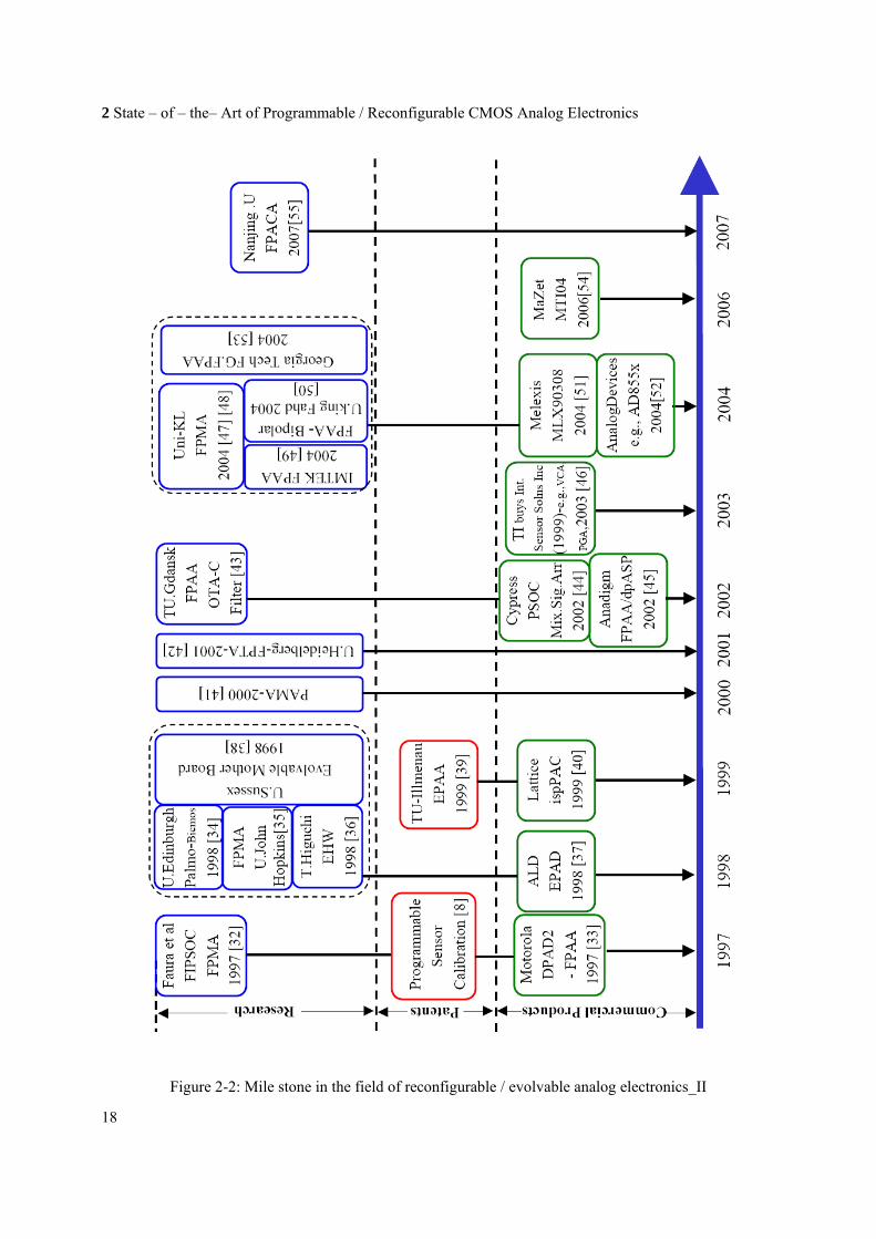
Figure 2-1: Mile stone in the field of reconfigurable / evolvable analog electronics_I
2 State – of – the– Art of Programmable / Reconfigurable CMOS Analog Electronics
18
Figure 2-2: Mile stone in the field of reconfigurable / evolvable analog electronics_II

19
2.2 Overview of Commercial Programmable Analog / Mixed-Signal IC’s
IC suppliers have devised various ways of creating configurable programmable analog ICs. The simplest uses traditional analog components in the input and feedback networks (resistors and capacitors). This option creates a continuous-time circuit, so-called because input signals are continuously used and output signals are continuously valid. The drawback is that, the parameters of filters implemented in this way usually depend on RC time constants, and resistors and capacitors implemented in ICs have large tolerances due to manufacturing deviations, making it difficult to achieve consistent filter performance. One way to solve the problem is to modify the circuit so that time constants depend rather on an amplifier’s transconductance. Lattice Semiconductor combines this technique with capacitor trimming (switched capacitor technique) to achieve filters with less than ±5% variation on their ispPAC chips [40]. More information about this chip and other available programmable chips will be discussed in subsequent titles.
2.2.1 IMP- Electrically Programmable Analog Devices (EPAC)
In 1995 IMP Inc. released a commercial FPAA-like product, the EPAC 50E10, and then released the EPAC 50E30 [Kle96]. Both are discrete-time designs based on switched-capacitor technology. Figure 2-3 shows a diagram of the 50E10 Electrically Programmable Analog Circuit (EPAC). It includes input analog multiplexer, programmable amplifiers, routing bus, and output modules. The input and output blocks can add programmable offsets. The input multiplexer can route either 16 single-ended or 8 fully-differential signals. The EPAC 50E10 is programmed using a 200-bit configuration bit string. Bandwidths are limited to 125 kHz (clock frequency of 1MHz) due to the use of switched-capacitor technology. The 50E10 is targeted to signal conditioning applications; the 50E30 is targeted to monitoring applications, with an alarm signal triggered if an input signal goes outside a programmable voltage range. All three designs can be reconfigured on the fly, by exchanging configuration bits between the SRAM configuration shift register and an EEPROM on-chip memory. This exchange takes 250 ms for the 50E10. The first implementation of EPAC technology is based on a 1.2 micron analog EECMOS process. The EPAC family of FPAAs is no longer commercially available. The basic time discrete macro building modules for Switch Capacitor approach were called as expert cell functional modules. The first implementation of first EPAC technology was based on 1.2 µm process with supply voltage of 5V with ± 10% of variations.
2.2.2 Motorola MPAA020
In 1997 Motorola Inc. released a CMOS switched-capacitor FPAA design called the MPAA020. The FPAA architecture, organized as an array of CABs, is depicted below. The FPAA includes

2 State – of – the– Art of Programmable / Reconfigurable CMOS Analog Electronics
20
Figure 2-3: Block diagram of a user programmable analog signal conditioning device from [22]
four rows of five CABs and is programmed using a 619-bit string. Each CAB can realize a first-order filtering functions. A CAB can be connected to its immediate neighbours through the “local inputs” and “local outputs.” It can also be connected to its other neighbours via a global bus accessed through the “global bus” input and “global outputs.” As with the EPAC family, the clock speed is 1MHz, limiting bandwidths to 200 KHz. A PC-based CAD tool accompanies the MPAA020. Programming of the MPAA020 is done via the serial port of a PC. Figure 2-4 shows the architecture of MPAA and this product is no longer commercially available.
2.2.3 Zetex Totally Reconfigurable Analog Circuit
Zetex has introduced the Totally Reconfigurable Analog Circuit (TRAC020), a continuous-time, log-domain bipolar design operating up to 4MHz. The TRAC includes 20 CABs, organized in two rows of 10 CABs, each capable of implementing one of the eight following functions: log, anti-log, non-inverting pass, addition, negating pass, op-amp, half-wave rectification, and off. The interconnection network is hardwired. The leftmost pins act as inputs whereas the rightmost pins act as outputs [31]. The intermediate pins can be configured either as inputs or outputs, depending on the configuration of the CAB to the immediate left of the pin. Topological programming is implemented by turning CABs off, and by external wiring of the pins. By turning a CAB off, its inputs and output are electrically disconnected, allowing the designer to use the output as an input to the subsequent CAB. Amplifier gain is determined by using off-chip
21
resistors. Configuration of the CABs is accomplished using a 60-bit string. Once more, a CAD tool is used to configure the TRAC; the CAD tool includes a simulator to simulate a circuit before being downloaded onto the FPAA IC. FAS advocate a computational approach to analog circuit design, where circuits are designed with their functionality in mind (a top-down approach), rather than the underlying circuitry (a bottom-up approach).
Figure 2-4: Architecture of MPAA
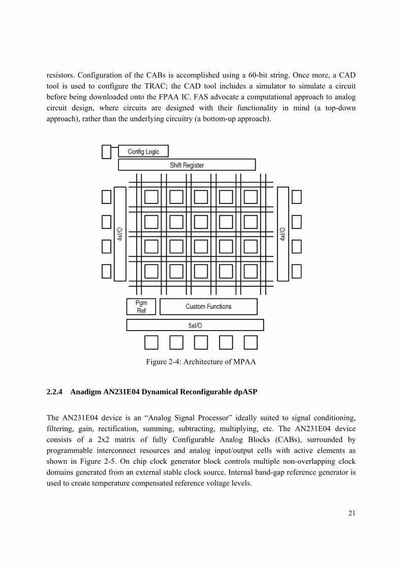
2.2.4 Anadigm AN231E04 Dynamical Reconfigurable dpASP
The AN231E04 device is an “Analog Signal Processor” ideally suited to signal conditioning, filtering, gain, rectification, summing, subtracting, multiplying, etc. The AN231E04 device consists of a 2x2 matrix of fully Configurable Analog Blocks (CABs), surrounded by programmable interconnect resources and analog input/output cells with active elements as shown in Figure 2-5. On chip clock generator block controls multiple non-overlapping clock domains generated from an external stable clock source. Internal band-gap reference generator is used to create temperature compensated reference voltage levels.

2 State – of – the– Art of Programmable / Reconfigurable CMOS Analog Electronics
22
Figure 2-5: Architectural overview of the device AN231E04 (from [45])
The inclusion of an 8x256 bit look-up table enables waveform synthesis and several non-linear functions. Configuration data is stored in an on-chip SRAM configuration memory. The AN231E04 device features seven configurable input/output structures each can be used as input or output, 4 of the 7 have integrated differential amplifiers. There is also a single chopper stabilized amplifier that can be used by 3 of the 7 output cells. Circuit design is enabled using Anadigmdesigner2 software, a high level block diagram based circuitry entry tool. Circuit functions are represented as CAMs (Configurable Analog Modules) these are configurable block which map onto portions of CABs. The software and a development board facilitate instant prototyping of any circuit captured in the tool.

23
2.2.5 Texas Instruments – PGA- Digital Trim for Non-Linearity’s
The PGA309 is a programmable analog signal conditioner designed for bridge sensors. The analog signal path amplifies the sensor signal and provides digital calibration. The calibration is done via a digital serial interface. The calibration parameters are stored in external non-volatile memory (typically SOT23-5) to eliminate manual trimming and achieve long-term stability. The all-analog signal path contains a 2x2 input multiplexer (mux), auto-zero programmable-gain instrumentation amplifier, linearization circuit, voltage reference, internal oscillator, control logic, and an output amplifier. Programmable level shifting compensates for sensor DC offsets. The core of the PGA309 (externally programmable gain amplifier) is shown in Figure 2-6.The gain of amplifier is defined by an external resistor. The overall gain of the Front-End PGA + Output Amplifier can be adjusted from 2.7V/V to 1152V/V.
Figure 2-6: Modern digital trimming for nonlinearities using PGA309 – programmable sensor signal
conditioner (from [46])
2.2.6 Analog Devices – Digi Trim AD855x series
The AD8555 is a zero-drift, sensor signal amplifier with digitally programmable gain and output offset. Designed to easily and accurately convert variable pressure sensor and strain bridge outputs to a well-defined output voltage range, the AD8555 also accurately amplifies many other differential or single-ended sensor outputs. Functional block diagram of sensor signal block diagram is shown in Figure 2-7. The AD8555 uses the ADI patented low noise auto-zero and DigiTrim® technologies to create an incredibly accurate and flexible signal processing solution in a very compact footprint. Gain is digitally programmable in a wide range from 70 to 1,280

2 State – of – the– Art of Programmable / Reconfigurable CMOS Analog Electronics
24
through a serial data interface. Gain adjustment can be fully simulated in-circuit and then permanently programmed with proven and reliable poly-fuse technology. Output offset voltage is also digitally programmable and is ratio metric to the supply voltage. In addition to extremely low input offset voltage and input offset voltage drift and very high dc and ac CMRR, the AD8555 also includes a pull-up current source at the input pins and a pull-down current source at the VCLAMP pin. This allows open wire and shorted wire fault detection. A low-pass filter function is implemented via a single low cost external capacitor. Output clamping set via an external reference voltage allows the AD8555 to drive lower voltage ADCs safely and accurately.
Figure 2-7: Functional block diagram of digitally programmable sensor signal amplifier (from [52])
When used in conjunction with an ADC referenced to the same supply, the system accuracy becomes immune to normal supply voltage variations. Output offset voltage can be adjusted with a resolution of better than 0.4% of the difference between VDD and VSS. A lockout trim after gain and offset adjustment further ensures field reliability. The AD8555AR is fully specified over the extended industrial temperature range of −40°C to +125°C. Operating from single-supply voltages of 2.7 V to 5.5 V, the AD8555 is offered in the narrow 8-lead SOIC package and the 4 mm × 4 mm 16-lead LFCSP. Other programmable devices from the manufacturer are programmable Gain instrumentation amplifier (G=1, 10, 100, 1000) AD8253

25
2.2.7 Lattice ispPAC
The ispPAC®30 is a member of the Lattice family of In-System Programmable (ISP™) analog integrated circuits. It is digitally configured via SRAM and utilizes E2CMOS memory for non-volatile storage of its configuration. The flexibility of ISP enables programming, verification and unlimited reconfiguration, directly on the printed circuit board. The ispPAC30 is a complete front end solution for data acquisition applications using 10 to 12-bit ADC's.
Figure 2-8: Functional block diagram of ispPAC family (from [40])
It provides multiple single-ended or differential signal inputs, multiplexing, precision gain, offset adjustment, filtering, and comparison functionality. It also has complete rout ability of inputs or outputs to any input cell and then from any input cell to either summing node of the two output amplifiers. Designers configure the ispPAC30 and verify its performance using PAC-Designer®, an easy to use, Microsoft Windows® compatible development tool. Device programming is supported using PC parallel port I/O operations. The device consists of 4 Instrumentation Amplifier, Two 8-bit multiplying ADC, and 2 configurable rail to rail output amplifiers (single -ended output, 0V-5V output swing, and 5V supply voltage) operating in as amplifier, comparator, filter or integrator modes. The block diagram of the ispPAC family is shown in Figure 2-8.
2.2.8 Cypress PSoC
The PSoC™ family consists of many mixed-signal arrays with on-chip controller devices. A PSoC device includes configurable blocks of analog circuits and digital logic, as well as programmable interconnect.

2 State – of – the– Art of Programmable / Reconfigurable CMOS Analog Electronics
26
Figure 2-9: Top level block diagram of PSOC (from [44])
This architecture allows the user to create customized peripheral configurations, to match the requirements of each individual application. Additionally, a fast CPU, Flash program memory, SRAM data memory, and configurable input/ output (IO) are included in a range of pin outs. The functional block diagram of PSoC is shown in Figure 2-9.

27
2.2.9 Analog Linear Devices – EPAD
ALD EPAD Matched Pair MOSFET: Array: EPAD is a MOSFET semiconductor with electrically settable threshold voltage. As a versatile circuit design element, the ALD EPAD is an analog transistor with built-in permanent memory. Used as an in-circuit element for trimming a combination of analog voltage and/or current characteristics, an EPAD can be remotely and automatically programmed using a PC-based EPAD Programmer via software control. Once programmed, the set DC voltage and current levels are stored indefinitely, even after power-down. The EPAD MOSFET array product family is available in 3 separate categories, the first is the ALD110800/ALD110900 zero threshold mode EPAD MOSFET’s. Second category is the enhancement mode EPAD MOSFET’s namely ALD1108xx/ALD1109xx and the third category is the ALD1148xx/1149xx depletion mode EPAD MOSFET’s.
ALD EPAD Op-Amps: are pre-trimmed electrically at the factory for very low offset voltage (Vos) and bias/offset currents (Ibias/Ios). They are ready to be used without any extra handling. These CMOS Op-Amps are economical, very-high-precision and easy-to-use. They also possess optional capability for all solid-state Vos field-trimming. EPAD Op-Amps are available in two grades, standard and E-grade. E-grade Op-Amps are specified with added electrical Vos programming ranges
2.2.10 Melexis – Programmable sensor interface MLX90308
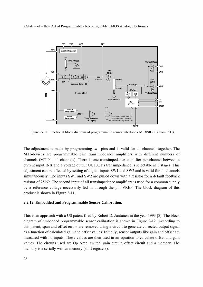
The MLX90308 is a signal conditioning microcontroller for sensors in bridge or differential configurations. Sensors that can be used include thermistors, strain gauges, load cells, pressure sensors, accelerometers, etc. The signal conditioning includes gain adjustment, offset control, and linearity compensation. Compensation values are stored in EEPROM and are reprogrammable. The application circuits can provide an output of an absolute voltage, relative voltage, or current. A supply voltage ranging from 6V-35 VDC can be applied. An internal voltage regulator fix the voltage to a typical value of 4.75V.The –3dB bandwidth of this product is 3.5 KHz. The functional block diagram of MLX90308 is shown in Figure 2-10.
2.2.11 MaZeT – Programmable Gain Transimpedance amplifier MTI04Bx-BF
The MTI-devices are a family of integrated circuits of programmable gain transimpedance amplifiers with different numbers of channels (4 standard, others custom specific). The MTI-devices are mainly used for signal conditioning of sensors with current outputs. They are especially suitable for connection of photodiodes of array and row sensors. The possibility to adjust the transimpedance in 3 steps is a special feature.
2 State – of – the– Art of Programmable / Reconfigurable CMOS Analog Electronics
28
Figure 2-10: Functional block diagram of programmable sensor interface - MLX90308 (from [51])
The adjustment is made by programming two pins and is valid for all channels together. The MTI-devices are programmable gain transimpedance amplifiers with different numbers of channels (MTI04 – 4 channels). There is one transimpedance amplifier per channel between a current input INX and a voltage output OUTX. Its transimpedance is selectable in 3 stages. This adjustment can be effected by setting of digital inputs SW1 and SW2 and is valid for all channels simultaneously. The inputs SW1 and SW2 are pulled down with a resistor for a default feedback resistor of 25kΩ. The second input of all transimpedance amplifiers is used for a common supply by a reference voltage necessarily fed in through the pin VREF. The block diagram of this product is shown in Figure 2-11.
2.2.12 Embedded and Programmable Sensor Calibration.
This is an approach with a US patent filed by Robert D. Juntunen in the year 1993 [8]. The block diagram of embedded programmable sensor calibration is shown in Figure 2-12. According to this patent, span and offset errors are removed using a circuit to generate corrected output signal as a function of calculated gain and offset values. Initially, sensor outputs like gain and offset are measured with no inputs. These values are then used in an equation to calculate offset and gain values. The circuits used are Op Amp, switch, gain circuit, offset circuit and a memory. The memory is a serially written memory (shift registers).

29
Figure 2-11: Block diagram of multi-channel programmable gain transimpedance amplifier (from [54])
Figure 2-12: Block diagram of embedded programmable sensor calibration (from [8])

2 State – of – the– Art of Programmable / Reconfigurable CMOS Analog Electronics
30
2.3 Overview of Academic Reprogrammable Analog Hardware
2.3.1 FPAA - University of Toronto (Gulak)
Gulak and Lee, in their earlier contribution to FPAA based on MOSFETs working in subthreshold [14], pass transistors were used and were controlled by SRAM memory cells. They also noticed that there were die to die variations in the performance of this FPAA. The IC was designed to implement both voltage and current mode circuits and was implemented for parametrically reconfigurable neural networks applications. Later, MOS transconductor based FPAA was implemented [6]. It consists of Op Amp and programmable capacitors linked by transconductor based interconnections. The innovation in this approach is that the switches in the interconnection network are linear resistors which are implemented as four transistor MOS transconductor. This IC was implemented in 1.2 µm CMOS technology.
Later on, Glen Gulak and Lee of Toronto University research group has presented two other FPAAs. The first FPAA consists of fully-differential continuous-time CMOS transconductor-based CABs operating in the 100 kHz range. This FPAA was targeted toward signal processing applications in the audio range with bi quad filter as shown in Figure 2-13(a) [5]. The CABs of this FPAA contain an op-amp as well as switchable feedback capacitors, and can also be used to implement a comparator by turning off the compensation capacitor. In this design, switches in the interconnection network are implemented using the transconductor, which acts as a programmable on/off switch, polarity change switch, and variable resistor as shown in Figure 2-13(b). The transconductor is also used to realize a four quadrant multiplier. Gaudet and Gulak presented another FPAA that is based on current conveyors. This FPAA is targeted toward applications in the video frequency range (10 MHz). Each CAB of the FPAA consists of a second generation current conveyor CCII and a bank of programmable resistors and capacitors.
2.3.2 Palmo- University of Edinburgh
The research group of the University of Edinburgh has devised a coarse grained FPAA chip called palmo. This chip basically works on pulse based techniques. In palmo the signals are represented neither as voltages nor as currents, but instead as digital pulses to represent discrete analog signals. The word palmo stands for pulsebeat, pulse palpitation or series of pulses. The chip consists of an array of programmable cells that performs the function of an integrator. The typical palmo cell is represented as shown in the Figure 2-14. The input pulses are integrated over time by the use of an analog integrator. This integrated value is then compared to a ramp in order to generate the pulsed output. The so compared ramp signals are global or local signals. The advantage of using such a ramp generation is that it is possible to accurately control the overall gain of the circuit. The palmo system allows the use of digital circuits to manipulate the pulses representing the analog quantities.

31
(a) (b)
Figure 2-13: schematic of bi quad filter (a) and schematic of MOS transconductor (b) [5]
Figure 2-14: Representation of typical Palmo Cell

2 State – of – the– Art of Programmable / Reconfigurable CMOS Analog Electronics
32
2.3.3 Evolvable Motherboard – University of Sussex
Figure 2-15: Evolvable motherboard test bed for the study of intrinsic HW (from [38])
The research group at the University of Sussex had developed a tool intended for implementing evolutionary exercises. The board level tool allows large variety of components to be used as basic active elements. The components are connected to each other through an interconnection architecture, namely analog switches. The Evolvable motherboard in total has 1500 switches. The diagonal lines in the Figure 2-15 represent the switches. Different plug in daughter boards are connected is also shown in the same figure. The users can choose the type of components to be added to the plug in boards like for e.g., transistors, multiplexers, operational amplifiers etc.

33
2.3.4 PAMA Catholic University of Rio de Janeiro
The programmable Analog Multiplexer Array (PAMA) is a fine grained, board level FPAA. This work has been inspired from the previous work of JPL group. The reconfigurable circuits are divided into three layers as shown in Figure 2-16. The three different layers constituting PAMA are discrete components, analog multiplexers and analog bus. The idea of a programmable multiplexer array was first in Zebulum et al [91] [92]. Each line of the analog bus corresponds to one interconnection point of the circuit; some of them can be associated to I/O signals or power signals, while others are associated to interconnection of the circuits. To put in simple sentences, each component terminals require one analog multiplexer. In PAMA, evolutionary techniques are able to exploit any interconnection patterns to realize different circuit topologies.
Figure 2-16: Analog reconfigurable circuit’s layers (from [56])
2.3.5 Higuchi EHW
The proposed EHW chip was meant for filters operating in intermediate frequencies. The basic idea of the EHW chip is shown in the figure below. The chip consists of 39 transconductance amplifier whose value could be determined genetically. The values, which actually control the base current of the CMOS, are coded as configuration bits. Each Gm element value may differ from the target value up to a maximum of 20%. Initial simulations have shown that 95% of the chips can be corrected to satisfy the IF filter’s specifications. The basic idea of the analog EHW is shown in Figure 2-17.

2 State – of – the– Art of Programmable / Reconfigurable CMOS Analog Electronics
34
Figure 2-17: Basic idea of the analog EHW chip for intermediate frequency filters (from [36])
2.3.6 FPAA – IMTEK
The FPAA structure consists of a two-dimensional array of CABs, which include digitally configurable transconductors (differential transconductance amplifiers). The Figure 2-18 shown below represents 1 programmable Gm cell. Figure 2-19 shows 1 CAB. The arrangement in a hexagonal layout allows reconfigurable routing of analog signals throughout the chip. Series and parallel connection as well as feedback of any order is provided by the structure. Every CAB has six branches connecting to the respective neighbour CABs and one for self-feedback. The massive parallel connections of both parasitic input capacitances as well as parasitic output capacitances at the input nodes of each CAB sum up to capacitances in an order of magnitude such that they are suitable as integrating capacitances for the filter up to unity-gain bandwidths of 200 MHz Different filter types with different orders can be synthesized on this FPAA, like for example second order low-pass filter, integrator or fourth order bi-quad Butterworth band-pass filter. A test-chip has been designed and manufactured in a 130nm CMOS technology.
2.3.7 FPTA / SRAA– JPL
Field programmable Transistor Array is a fine grained FPAA developed at the Jet Propulsion Laboratories, intended to conduct experiments in evolvable hardware. FPTA is a reconfigurable hardware at the transistor level. FPTA is an array of transistors interconnected by programmable switches as shown in Figure 2-20(a). The status of the switches ON or OFF determines the circuit topology. FPTA remains a good platform for synthesis of analog, digital and mixed signal

35
circuits. Figure 2-20 illustrates a module of the programmable transistor array consisting of 8 transistors and 24 programmable switches. This module consists of PMOS and NMOS transistors, and switch based connections.
Figure 2-18: Block diagram of a programmable Gm-C cell (from [57])
Figure 2-19: Block diagram of a configurable analog block (from [57])

2 State – of – the– Art of Programmable / Reconfigurable CMOS Analog Electronics
36
The number of switches used in realising different circuit topologies may differ from each other. The two FPTA chip versions were implemented in 0.5µm CMOS technology and one in 0.18µm technology. The group manufactured 3 versions of FPTA chips of varying complexity [63]. The most recent FPAA version is called Self Reconfigurable Analog Array (SRAA). This version of the chip has variety of analog cells like Op Amp, comparators, pulse width modulators etc., together with the possibility of self correction at extreme temperatures ranging from –180°C to +125°C [67]. In SRAA, digital ASIC implements the compensation algorithm and the control of analog ASIC during monitoring and compensation mode. A hierarchical compensation approach was adapted. Three different levels of compensation were carried out. First, involves through mapping corrections that were predetermined by a model based or through measurement. Secondly, finding solution through gradient descent search and third approach is by global search using evolutionary approach. The block diagram of the compensation and monitor control are shown in Figure 2-20(b)
(a) (b)
Figure 2-20: Module of the programmable transistor array (from [56] & [67])
2.3.8 FPTA – University of Heidelberg
The vision group at the University of Heidelberg had developed a fine grained FPAA approach called FPTA, a system suitable for hardware evolution of analog electronics circuit at transistor

37
level. The CMOS VLSI chip manufactured in 0.6µm technology consists of 16*16 programmable transistor cells as shown in Figure 2-21. These cells contain only active devices, either a programmable PMOS or NMOS transistors, whose aspect ratio can be changed. The channel width and length of the programmable transistor itself can be adjusted to W = 1. . . 15µm and L = 0.6, 1, 2, 4, 8µm, respectively [58]. The terminals of these transistors can be connected to four neighbouring cells with the help of the switches. By appropriate programming of these switches, different circuit topologies can be implemented. The configuration of the transistor array is stored in SRAM cells embedded in the transistor cells themselves. The chip was used for automatic synthesis of analog circuits using evolutionary approach.
Figure 2-21: Simplified architecture of FPTA - Heidelberg chip (from [58])
In spite of good results, the approaches mentioned in section 2.3.8 and in section 2.3.7 uses sea of transistors (tremendous area requirement) for implementing circuits using large amount of switching devices affecting the frequency behaviour of the whole system. These pitfalls remain as the incentives of this thesis work.

2 State – of – the– Art of Programmable / Reconfigurable CMOS Analog Electronics
38
2.3.9 EPAA – TU Ilmenau
Electrically Programmable Analog Array (EPAA) is a fully configurable analog array dedicated to implementation of analog and mixed-signal applications using both, continuous current (CC) and switched-capacitor (SC) techniques. Overall architecture can be seen in Figure 2-22. Partitioning to 4 clusters (each containing 4 cells) can be seen in the right-upper part. Desired EPAA configuration is autonomous downloaded via serial system interface from EEPROM, immediately after power-on sequence. EPAA architecture consists of 4 clusters and each cluster has 4 cells as shown in the figure below. Initial version of EPAA was implemented in Alcatel Mietec 0.5um CMOS technology, comprising 2x2 programmable clusters. Typical supply voltage of 3.3V was used. The EPAA was used in application circuits like magneto resistive bridges. EPAA along combined with dedicated software to form the evaluation platform called Rapid Development Kit (RDK).
Figure 2-22: Architecture of EPAA (from [39])

39
2.3.10 FG FPAA – Georgia Tech
As seen in Figure 2-23, the RASP 1.x FPAA is composed of two vertically aligned general purpose configurable analog blocks (CABs) connected via a single crossbar switching network. This switch matrix (SM) allows any CAB component in either CAB to be connected to any other CAB component with just two switches. The CAB components were chosen to provide a balanced mixture of granularity in order to achieve an effective trade-off between performance and flexibility. The transistors and capacitors provide fine-grain flexibility, which allows almost any circuit to be synthesized with a sufficiently large CAB array. OTAs and C4 band-pass elements were included as medium-grain components, since these elements can be used in a significant number of circuit topologies. FPAA architecture has two modes of operation, run and program. In program mode, indicated by the “prog” signal going high, the floating gate transistors used for switches and biases are configured into one large matrix for global addressing.
Figure 2-23: RASP. 1. x FPAA architecture and CAB components (from [53])
In this approach a pull-up transistors drive the sources of floating gate switch transistors, and drain lines are connected to the column programming logic. Bias transistors are disconnected from the circuits they control and are connected to the same programming lines used for the switches. The row selection circuitry is used to switch the external coupling voltage, VC, to the selected row. All unselected rows have their coupling capacitors pulled up to VDD. A decoder is used to generate the row select signals, rsel<x>. In a similar fashion, the column selection circuitry connects the selected column’s drain line to the external drain signal, VD. All unselected drain lines are tied to VDD. Another decoder generates the column select signals, csel<x>. Run mode is defined when the “prog” signal in Figure is low. In this configuration, the source and drain terminals of the floating gate switches are left floating as the rows and columns of the routing fabric, and the bias floating gate transistors are switched into their corresponding CAB components. In this work several filter topologies were investigated.

2 State – of – the– Art of Programmable / Reconfigurable CMOS Analog Electronics
40
2.3.11 FPAA Based OTA-C Filter - Technical University of Gdansk
(a)
(b)
Figure 2-24: Programmable current mirror (a) programmable OTA (b) (from [43])
Bogdan Pankiewicz et al had investigated and analysed a programmable OTA. This programmable OTA along with programmable capacitors were used to realize CAM’s and then to filter circuits using these CAM’s. CMOS switches assist in programming the structure. Programmable OTA is obtained by using programmable current mirrors. The current mirror has 5 output stages (1, 2, 4, 8, and 16). Appropriate switch selection gives the essential current defining the currents. The programmable current mirror was focused to adjust only gain [43]. Figure 2-24(a) and Figure 2-24(b) shows CMOS programmable OTA and programmable current mirror circuits respectively.

41
2.3.12 FPMA - John Hopkins University
(a)
(b)
Figure 2-25: Configurable analog module (a) pulse shaping chain using array of CAM (b) [35] [83]
The architecture of an FPMA* (Field Programmable Mixed Signal Array) is largely determined by the type of programmable interconnection technology. An anti-fuse technology provides a low resistance programmable connection and nonvolatile configuration storage in a structure in the size of a via. An FPMA architecture based on anti-fuses can implement continuous time analog circuits, as well as discrete time circuits. The programmable analog modules can be much more area efficient, because anti-fuses occupy much less area than a MOS switch. In this approach, AMOD (analog modules) architecture is based on a non-programmable fully differential Op Amp with associated programmable MOS capacitor and poly resistor arrays, as well as some MOS
* Same abbrevation like the one used in this thesis (chapter 4) but has different meaning.

2 State – of – the– Art of Programmable / Reconfigurable CMOS Analog Electronics
42
analog switches for implementing switched circuits as shown in Figure 2-25(a). The CAM is used to build pulse shaping chain as shown in Figure 2-25(b) [35] [83].
2.4 Evolvable Hardware
Evolvable hardware is basically reconfigurable circuits that can inherit the property of living organisms through the application of some evolutionary techniques like Genetic Algorithm (GA). Conceptually, all reconfigurable hardware devices irrespective of granularity (fine grained, medium grained or course grained) can be subjected to learning or evolutionary optimization procedures. The hardware structures can be for digital or analog domain. Some reprogrammable hardware used in today’s evolutionary techniques is as listed below.
1. Field Programmable Gate Arrays (FPGA) for digital domain [65].
2. FPAA for analog domain [57].
3. FPTA for both analog and digital structures at transistor level [63] [64].
4. Evolvable Micro Electro-Mechanical System (MEMS) [66].
5. Evolvable Analog Neural Network [68]
Recent trends in analog circuit synthesis uses evolutionary approaches for device sizing, topology determination, etc. [72], Evolutionary approaches are stochastic search procedures employing bio–inspiration. These approaches are widely used in engineering applications in research as well as in industries [69] [70] [71]. Working of Evolvable Hardware (EHW) is based on combination of evolutionary approaches and reconfigurable devices as shown in Figure 2-26, thereby inheriting the self-x properties from evolutionary approaches to the hardware [73]. The self–x characteristics refer to self-organisation, self-adaptation, self-healing, self-diagnosis, etc. These desirable properties make it more attractive to modern intelligent and hybrid sensor systems.
Figure 2-26: Representation of evolvable hardware

43
Table 2-1: State of the art of programmable analog electronics S.
Nr
Con
trib
utio
n
Spec
ial/P
rodu
ct
Nam
e
Prog
ram
mab
ility
Gra
nula
rity
&
Con
fig D
ownl
oad
App
licat
ion
Cir
cuit
switc
hes
Ban
dwid
th
Tec
hniq
ue
Tec
hnol
ogy
1 Precision Monolithics Inc. [10] GAP-01 Gm_ Amplifier Coarse Current mode
switches [10] 15 KHz
2 Tsividis et al Analog Signal
Processor (ASP)
Bi-quad filter Transmission Gate
sampling rate of 16 KHz
Time continuous [77]
3 Czamul et al MRN(MOS
resistive network)
4 matched mos resistor integrator Time
continuous[11] MOS
4 Sivilotti et al Proto-Chip SRAM Analog Neural Network
CMOS Transmission
Gates sub-threshold CMOS
1) FPAA Sub-threshold design SRAM reconf. Neural
networks pass transistor sub-threshold 1.2 µm CMOS
5 Lee & Gulak 2) FPAA Gm_ Amplifier app.ckt in audio
freq. Range 4 cross coupled mos transistors linear
1.2 µm
CMOS
6 Uni.Toronto
(Gulak) MADAR-
FPMA continuous time
7 IMP. Inc EPAC prog.amplifier 125 KHz time discrete, Switched Capacitor
1.2 µm EECMOS
8 Chang et al
MFSDB (multi fn Sig.
Detection block)
CMOS
Transmission Gate
1.2 MHz linear, Switched current CMOS

2 State – of – the– Art of Programmable / Reconfigurable CMOS Analog Electronics
44
9 Actel
10 Kawasaki resistor and capacitor array coarse
gain adjustment,
filter
Switching Station (TG) CMOS
11 Analogix FPAA 8-order elliptic bandpass filter, hundreds of
MHz Current-mode Bipolar
12 Kutuk, Kang
et al FPAA
3rd order LP filter &
4th order BP filter EPROM 125 kHz Switched capacitor
13 Premont et al FPAA prog. Cap & Res several kHz to few MHz
continuous time, CCII conveyor
14 E. S. Sinencio et al Current mode FPAA
CAC (Conf.analog cells)
different types of integrator,
filter
MOS transistor switches CMOS
1) FPTA fine, RAM TG CMOS 15 JPL
2) SRAA coarse
16 Fraunhofer IPMS Analog Bread Board 200 kHz time continuous BiCMOS
17 ZeteX TRAC Coarse, Shift Register CMOS
18 Faura et al FIPSOC prog. gain,
filtering coarse
19 Motorola MPAA SRAM programmable switches 200 kHz Switched Capacitor CMOS
20 Uni. Edinburgh Palmo BiCMOS
21 Uni. John Hopkinson FPMA(field prog.mixed-signal array)
Diff. amplifier AMODs
(analog Modules)
anti-fuse 20MHz continuous time anti-fuse CMOS, 0.22µm
22 T.Higuchi et al Gm Amplifier IF Filter, EHW band pass = 21 kHz-455 KHz CMOS

45
23 Uni. Sussex Evolvable
Motherboard
(EM) fine Evolvable HW board level
24 Analog Linear Device EPAD prog.Vth, prog.current mirror
Vos user trimmed signal
condt. 2.1 MHz CMOS
25 Lattice ispPAC conf. Amps, 7 filter frequency
coarse, SRAM
prog. Signal conditioning
GBW=15 MHz, filter=50K-600
KHz
26 PAMA FPAA using discrete components fine board level
27 Uni.
Heidelberg FPTA Digital & Analog fine, RAM EHW
transmission
gate time continuous CMOS
28 TU.Gdansk FPAA OTA prog. Current mirror OTA-C filter 60KHz &
500kHz BP CMOS
29 Cypress PSoC- Mixed signal array time continuous, SC
30 Anadigm dpASP 2*2 CAB SRAM
PGA 309 External resistor Bridge sensors, gain adjustment hundred's kHz
31 Texas
Instruments XTR108
32 Uni-KL FPMA, FPMA2
In_Amp, FC, Miller, Diff O/P.
medium, Serial
Dyn. sensor signal
calibration,
EHW
Transmission
gate 1.55 MHz
time continuous
& sub-threshold 0.35µm , CMOS
33 IMTEK FPAA coarse Gm-C Filter, EHW 164 MHz 130nm,
CMOS
34 Uni. King Fahd FPAA Filter Time-continuous, current mode
Bipolar
(CAM)
35 Georgia Tech FPAA- l i G
filter Floating Gate Few kHz

2 State – of – the– Art of Programmable / Reconfigurable CMOS Analog Electronics
46
Floating Gate ( 20KHz_-3dB)
36 Melexis
Programmable sensor
Interface
(MLX90308)
EEPROM gain
adjustment, offset ctrl, etc
37 Analog Devices DigiTrim AD855x gain and Vos
Trimming poly fuse
38 MaZet MT104 Gm_amplifier
39 Uni.Nanjing FPACA JPL like cell but extended with R,C fine cmos
40 Pilkington
Motorola
Switched
capacitor
41 National, AD, ST, MAXIM VGA Gain amplifier
42 AD ADN2850 prog.resistor
43 MAXIM MAX1474 prog.capacitor signal conditioning
44 Xicor, (Intersil) DCP, DCC, X90100
digitally controlled POT, & Capacitor

47
2.5 Discussion
From the state of the art of programmable, reconfigurable and evolvable analog circuits, realized at various levels (voltage/current) and modes (time discrete/ time continuous) of flexibility, interesting inferences and challenges yet open were identified and remains as an incentive for this work. They are as listed below,
1. Available Resource – flexibility. The thriving force to have shorter design cycles have led to the state of the art of programmable analog circuits. Where the flexibility of the pursued approaches vary widely ranging from fine, coarse and medium granular levels. For example, programmable OTA explained in section 2.3.11 were built using a programmable current mirror only and the rest of the devices constituting the OTA are unit non-programmable devices. The next level of programmability comes at the functional level as explained in section 2.3.12, where the fully differential amplifier (functional module) remains non-programmable but the devices in the feedback are instead programmable to define the gain, compensate offset, vary cut-off frequency etc. Some commercial products based on this approach are Anadigm, AD8555 from analog devices and PGA309 from Texas Instruments. Functional level approaches have selective specification programmability. Fine granular approaches like FPTA (JPL and Heidelberg research groups) on the other hand, have sea of transistors (homogeneous array). In this approach, transistors can be configured in such a way that it behaves like a resistor or capacitor, even though the area occupied by such realizations are less, linearity exhibited by such devices are challenging. These approaches do not support on chip programmable passive devices which are very important for realizing analog circuits with feedback arrangement. Transistor level granular (FPTA) approaches increases the cost by consuming large die area and adds parasitic elements.
2. Speed of Operation / Bandwidth limitation Most of the programmable approaches use CMOS switches for proving flexibility. Unlike the ideal switches, CMOS versions have definite on resistance and parasitic capacitances influencing the signal integrity of the system. Hence use of excessive switching resources, as in the case of FPTA’s, has tremendous limitations on the operating bandwidths. More is the number of switches used; less is the operating bandwidth and vice-versa. However, use of switching technologies like anti-fuse could help. More details about switching techniques are discussed in chapter 4.
3. Resource Usage / Utilization Depending upon the type of flexibility, the ratio of used area to available area would vary. The degree of resource utilization becomes high, when flexibility is less. On the contrary, if the flexibility is less then fault tolerance would also

0
48
be a question here. This could be understood by taking the example used for describing the different modes of granularity in the first discussion on the available resource section. Programmable OTA approach (section 2.3.11) has high resource utilization because of less flexibility. Coarse granular methods have medium range resource utilization. Whereas, fine granular approaches have very less resource utilization because of very high flexibility. Hence a trade off in flexibility of the realized system is very crucial for the cost point of view.
4. Power consumption In programmable approaches, irrespective of the level of usage (ON/OFF), the building blocks is always connected to supply rails inherently consuming power. Hence the power requirement of the system is increased. This issue is very crucial when the designed product is applied for battery driven products or medical applications.
5. Device matching. Accuracy of the devices in the manufactured chip is always very important. But after turnaround from the factory, manufacturing procedure and tolerances introduces variations in the design. Traditionally analog designers have used different technique like device matching to cope with this problem. Reconfiguration is another, reversible option implied by programmable devices.
6. Industrial needs – The state of the art of evolvable analog hardware approaches would find its place in industry, only if they obtained circuits that are established and predictable with respect to topologies and behaviors. Black box like structure with non-established and some time peculiar topologies from the state of the art evolvable analog approaches adds to the skeptism of the approach by the conservative designers.
7. Noise issues The noise issues remains a part of every system. Especially in programmable approaches, source of noise come from clock feed through of switching activity, noise due to supply rails, thermal effects etc.
So it can be inferred from the state of the art that there is yet no single analog evolvable hardware approach available with appropriate granularity for realizing signal conditioning electronics in modern and intelligent sensor system. The above listed open issues forms the basis for the research work pursued in this thesis. The conceptual representation of the challenges posed was shown in Figure 1-2.

49
3. Sensor Application Circuits Survey for Resource Distillation
We understand from state of the art of evolvable analog approaches that, using FPTA in particular (JPL chip & Heidelberg chip) have consumed very large die area in order to provide high flexibility in dimensions as well as in circuit structures. But we also understand from the discussion section in the chapter 2, that established circuit structure are mandatory for industrial point of view in accepting and applying the evolvable concepts especially to the field of sensor systems (signal conditioning in particular). Therefore for our goal of industrial applicability of the evolvable concepts with less cost emphasis, following steps/information are essential.
1. To analyze and understand the vital and key analog building blocks with topologies required for signal processing in any sensor systems.
2. To identify and realize signal processing/conditioning circuits through these established topologies.
3. To provide sizing flexibility for the chosen topology to compensate variations.
However, after identifying the importance of the fundamental analog building blocks (amplifiers), a survey was carried upon to find out various amplifier application circuits along with the sizing information of the feedback components. The sizing information obtained here is later on used for defining the flexibility range of out CAM at fine granular level for both active and passive scalable devices. The collection of the application circuits during the survey are elaborated in this chapter under various sub-sections. Finally, a classification is made based on their purpose of implementation. As discussed earlier, operational amplifier (Op Amp) is a vital fundamental block of analog electronics. The name “operational amplifier” comes from the use of this type of amplifier in performing several operations like adding, integrating, differentiating, etc. A simple CMOS operational amplifier is represented as shown in Figure 3.1.
Figure 3-1: Simple operational amplifier

3 Sensor Application Circuits Survey for Resource Distillation
50
The circuit topology constituting the amplifier can be realized in several technologies like bipolar, BiCMOS, purely CMOS, etc. In this work, we focus on CMOS topologies. The operation of an ideal amplifier is very simple. An ideal amplifier would produce an output which is the difference of the applied voltage in its two input terminals. In ideal conditions, these amplifiers have infinite gain, infinite input resistance, zero output resistance, zero offset etc. The output voltage produced by such an amplifier is represented as shown in Equation. 3-1. Where Vo is the output voltage, Vid is the difference in input voltage and Av represents the voltage gain of the circuit. This gain is also called as open loop gain. Some important performance parameters of operational amplifiers are, gain band width (GBW), Phase margin (PM), common mode range (CMR), common mode rejection ratio (CMRR), power supply rejection ratio (PSRR), slew rate (SR), etc. Its applications span the broad electronic industry filling requirements for signal conditioning, special transfer functions, analog instrumentation, analog computation, and special systems design.
AvVidVo = Equation 3-1
This chapter gives the overview of performance measurement circuits and most of the application circuit using operational amplifiers. Op Amp applications cover the broad electronic industry’s filling requirements for signal conditioning, special transfer functions, analog instrumentation, analog computation, and special systems design.
3.1 Introduction to Application Circuits A description of the ideal operational amplifier model was presented in the last section, and the introduction of complete application circuits may now begin. Though the ideal model may seem to be a bit far from reality - with infinite gain, bandwidth, etc., it should be realized that the closed loop gain relations that will be derived in this section are directly applicable to real circuits. A comprehensive collection of measurement and application circuits are listed out in Figure 3-2 [7] [78] [79] Feedback Technique: The precision and flexibility of the operational amplifier is a direct result of the use of feedback circuits. Generally speaking, amplifiers employing feedback will have superior operating characteristics at a sacrifice of gain [101]. With enough feedback, the closed loop amplifier characteristics become a function of the feedback elements

51
Figure 3-2: Some Op Amp measurement and application circuits

3 Sensor Application Circuits Survey for Resource Distillation
52
3.2 Basic Measurement Circuits
3.2.1 Inverting amplifier An inverting amplifier is built by grounding the positive input of the Op Amp and connecting resistors R1 and R2 in the so called feedback network as shown in Figure 3.3 (a). The closed loop voltage gain of the inverting amplifier is given by the Equation.3-2. This arrangement is also used as voltage reference circuit.
VinRRVout
12
−= Equation 3-2
3.2.2 Non-inverting amplifier A non inverting amplifier is built by feeding in the input to the positive terminal of the Op Amp and connecting resistors R1 and R2 in the so called feedback network as shown in Figure 3-3 (b). The closed loop voltage gain of the inverting amplifier is given by the Equation.3-4. This arrangement is also used as voltage reference circuit.
121
RR
VinVout
+= Equation 3-4
3.2.3 Output Voltage Swing Output voltage swing is measured by using the schematic described in inverting amplifier arrangement. The schematic is shown in Figure 3-3(a). A DC voltage sweep is performed at the input to view the voltage output swing.
3.2.4 Unity Gain Buffer or Voltage Follower Voltage follower is a type of circuit arrangement where the output voltage follows the input voltage level. The schematic representation of voltage follower is shown in Figure 3-3(d). The output voltage and voltage gain is given by Equation.3-5
VinVout = Therefore 1=Av Equation 3-5

53
(a) (d)
(b) (e)
(c) (f)
Figure 3-3: Operational amplifier basic measurement circuits

3 Sensor Application Circuits Survey for Resource Distillation
54
(a) (b)
Figure 3-4: Operational amplifier basic measurement circuits (continued)
3.2.5 Slew Rate Slew rate is a measure of rate of change of the output voltage. The voltage follower circuit can be used to determine this parameter.
3.2.6 Settling Time Settling time (Ts) is defined [105] as the time elapsed from the application of an ideal instantaneous step input to the time at which the closed loop amplifier output has entered and remained within a specified error band, usually symmetrical about the final value. Settling time includes a very brief propagation delay, plus the time required for the output to slew to the vicinity of the final value, recover from the overload condition associated with slewing, and finally settle to within specified error. The voltage follower circuit is used to determine this parameter.
3.2.7 Input Common Mode Range Input common mode range is measured using the circuit in Figure 3-3 (d) by sweeping the input voltage from VSS to VDD. This configuration is chosen because, in a high gain configuration, the output swing of the amplifier limits the linearity of the circuit. In the unity gain configuration, however, the linear portion of the curve represents the CMR of the amplifier.
3.2.8 Offset Voltage
(Vos) is the voltage measured at the output of an operational amplifier when the positive input is grounded in a unity gain arrangement.

55
3.2.9 Summing amplifier Summing amplifiers are used to combine signals. The schematic of summing amplifier is depicted in Figure 3.3 (e). Here, input voltage sources Vin1 and Vin2 are connected to the inverting terminal of the amplifier through resistors R1 and R2. The resistor R3 connects the output to the inverting input in a feedback arrangement. The output voltage of this summing amplifier is given by the Equation 3-6.
2231
13 Vin
RRVin
RRVout −−= Equation 3-6
3.2.10 Difference amplifier Difference amplifiers are the one which amplifies the difference in the applied voltage at the two terminals of the operational amplifiers as shown in Figure 3-3 (c). The output voltage is given by the Equation 3-7.In this equation, when R2=R1 then Vout = - (Vin1-Vin2) This circuit is sometimes called as differential subtraction [78].
)21(12 VinVin
RRVout −−= Equation 3-7
3.2.11 Open loop Frequency Response Open loop frequency response is the most difficult part to measure or simulate successfully, the reason is because of its high differential gain of the operational amplifier. Simulation or measurement of open loop gain will assist in characterising the open loop transfer curve, open loop output swing, phase margin, unity gain bandwidth, output resistance, and the dominant pole. A simple circuit as shown in Figure 3-1 is used. Another approach is shown in Figure 3-3 (f) [7]
3.2.12 Common Mode Rejection Ratio (CMRR) is defined as the differential mode voltage gain to common mode gain. The equation representing CMRR is given below. The schematic representation for determination of CMRR is shown in Figure 3-4 (a)
CMRRAvAc
AcAvAc
VcmVout 1
)2/(1=≅
−+= Equation 3-8
3.2.13 Power Supply Rejection Ratio (PSRR) is a parameter of the operational amplifier to measure its rejection capability of the noise in the power supply. Figure 3-4 (b) shows the schematic to determine this parameter. In this schematic a small sinusoidal voltage is inserted in series with Vdd / Vss to determine PSRR+ and PSRR- respectively. The PSRR+ and PSRR- can be denoted as shown in the Equation 3-9.

3 Sensor Application Circuits Survey for Resource Distillation
56
( )−
≅+
≅PSRRVss
VoutorPSRRVdd
Vout 11 Equation 3-9
(a) (b)
(c)
(d) Figure 3-5: Operational amplifier in signal conditioning circuits

57
3.3 Signal Conditioning
3.3.1 Filters
a) Active Single Pole Low Pass Filters A simple single pole low pass filter is represented in Figure 3-5(a). The gain calculation of the amplifier is extended from the resistive feedback arrangement shown in Figure 3-3(a). The transfer function can be represented as shown in Equation 3-10.
)()(
)(1
2
sZsZ
sAv −= Therefore )1(
1
1
2
H
sRR
Av
ω+
−= Where ωH= 2πFH = CR2
1 Equation 3-10
b) Active Two Pole Low Pass Filters A basic dual pole; low pass filter is represented in Figure 3-5(b) and is formed from an op amp with two resistors and two capacitors. Here op amp operates as voltage follower. The transfer function can be represented as shown in Equation 3-11. The frequency ωo is the cut off frequency.
A LP (s) = ω2o / ( S2 +S
Qoω
+ ω2o)
where, ωo = - 2121
1CCRR
and Q = 21
21
2
1
RRRR
CC
+
Equation 3-11
c) High Pass Filter with Gain A high pass filter with gain is represented in Figure 3-5(c) which is similar to the topology shown in Figure 3-5(b) only but by interchanging the position of the resistors and capacitors. Here, the unity gain arrangement is replaced with a non inverting gain of K [78]. The transfer function can be represented as shown in Equation 3-12. When R1=R2=R and C1=C2=C then,
A HP (s) = K(S2 / ( S2 +S
RCK−3 + 22
1CR
))
where, ωo = RC1 and Q =
K−31
Equation 3-12

3 Sensor Application Circuits Survey for Resource Distillation
58
d) Band Pass Filter A band pass filter can be realized by combining the low pass filter and high pass filter characteristics. One possible circuit for such a band pass filter is represented in Figure 3-5(d). The transfer function can be represented as shown in Equation 3-13.
A BP (s) = - ) w+
QS+ S ( o
2o211
22
31
3
ωωoS
CRCR
RRR+
where, ωo = 212
1CCRRth
and Q = 21
212
CCCC
RR
th +
Equation 3-13
3.3.2 Voltage Regulators One of the most common signal conditioner is the voltage regulator, which transforms a varying voltage into a constant voltage either for power supply or for referenced voltage applications. The desirable properties of high gain and power supply rejection ratios of Op Amp ensure precise voltage regulation. Voltage regulators are more usually consider operation from a single source of unregulated dc voltage source. One such voltage regulator [106] is shown in Figure 3-6 (a). The amplifier is biased to operate on a single unregulated power supply instead of dual power supplies with opposite polarities. The negative pin is grounded and positive is biased at the Zener voltage. The Zener diode Z1operates at constant load current, since the output current is given by the transistor Q1.The resistor RP is for short circuit protection, where the internal short circuit protection may not be sufficient. The Resistor RS provides current limiting to protect Q1. The line regulation is increased beyond that of the Zener by using the output voltage as excitation for the Zener.
3.3.3 Precision Current Sink and Current Source The precision current source and sink are shown in Figure 3-6(b), and Figure 3-6(c) respectively [79] [80]. The configurations shown will sink or source conventional current respectively. Caution must be exercised in applying these circuits. The voltage compliance of the source extends from Break down voltage of the external transistor to approximately 1 volt more negative than VIN. The compliance of the current sink is the same in the positive direction. The impedance of these current generators is essentially infinite for small currents and they are accurate so long as VIN is much greater than VOS (offset voltage) and IO is much greater than I bias. The source and sink illustrated in Figure 3-6(b) and Figure 3-6(c) use an FET to drive a bipolar output transistor. It is possible to use a Darlington connection in place of the FET-bipolar combination in cases where the output current is high and the base current of the Darlington input would not cause a significant error. The amplifiers used must be compensated for unity-gain and additional compensation may be required depending on load reactance and external transistor parameters.
59
3.4 Signal Processing
3.4.1 Linear Circuits
3.4.1.1 Voltage – to – Current Converters So far, we have considered voltage as the output of the inverting amplifier, but amplifier also finds wide application as a current supplying device. This is accomplished by placing the load in the feedback loop as in Figure 3-6 (d). Since the inverting input is ground potential, the current through RI is given in the Equation 3-14. No current flows into the inverting input, so the same current flows through RL. In similar configurations, the inverting amplifier can serve as a linear meter amplifier or deflection coil driver [101] [106].
11 R
VI in= Equation 3-14
3.4.1.2 Current – to – Voltage Converter Current may be measured in two ways with an operational amplifier. The current may be converted into a voltage with a resistor and then amplified or the current may be injected directly into a summing node. Converting current into voltage is undesirable for two reasons. First, impedance is inserted into the measuring line causing an error. Second, amplifier offset voltage is also amplified. The use of a current-to-voltage transducer avoids both of these problems. The current-to-voltage transducer is shown in Figure 3-6(e). The input current is fed directly into the summing node and the amplifier output voltage changes to extract the same current from the summing node through R. The only conversion error in this circuit is Ibias of amplifier is summed algebraically with Iin. This basic circuit is useful for many applications other than current measurement like amplifiers for photoconductive, photodiode and photovoltaic cells [80]. The converted voltage values are represented as in Equation 3-15.
RIVout in *= Equation 3-15
3.4.1.3 Differentiator Differentiator is a circuit which uses capacitor and resistor as shown in the Figure 3-6 (f). The output voltage is proportional to the value of R and C. The output voltage is given by the Equation 3-16.
dtdVinRCVout −= Equation 3-16

3 Sensor Application Circuits Survey for Resource Distillation
60
(a) (b)
(c) (d)
(e) (f) Figure 3-6: Operational amplifier in signal conditioning and signal processing circuits

61
3.4.1.4 Integrator Integrator is another useful building block constructed using an operational amplifier with frequency dependent feedback. Unlike the inverting amplifiers shown in Fig 3-3 (a), resistor R2 is replaced by a capacitor C as shown in Figure 3-7 (a). The output voltage is given by the Equation 3-17
∫−= dtVinRC
Vout .1 Equation 3-17
3.4.1.5 Charge Amplifier Capacitive microphones and some types of accelerometers operate on the principle of conversion of the measurement variable into an equivalent charge. The equivalent circuit of such a transducer may be represented by a battery and capacitor in series. This is represented in Figure 3-7(b). As the Capacitor varies, the charge also changes according to the Equation 3-18. When this transducer is connected to an inverting amplifier as in Figure 3-7(b) [106], this charge flows into the feedback capacitors CF. This resultant change in charge on CF generates an output voltage as given in Equation 3-19.
ECq 1∆=∆ Equation 3-18
FCECVout 1∆−= Equation 3-19
Resistor RF is necessary, since the amplifier requires a dc path from each input. In the absence of this resistor, the capacitor will build up a dc charge until the output voltage reaches saturation. This resistor limits the lower cut-off frequency of the charge amplifier. For stabilization and protection of the input stages, a series resistor R1 is inserted. The gain of the charge amplifier is given by the Equation 3-20.
FCE
CVout
−=∆ 1
Equation 3-20
3.4.1.6 Reference Voltage Source High input impedance and easily adjustable gain of operational amplifier are utilised so as to make it as a reference voltage source. The inverting and non-inverting arrangement of operational

3 Sensor Application Circuits Survey for Resource Distillation
62
amplifier discussed earlier can be extended to create referenced voltage source with Zener diodes for positive and negative voltage values as shown in Figure 3-7(c) and Figure 3-7(d) respectively [106]. The output voltages for both the cases are given in Equation 3-21. The loading conditions on Zener diode are constant. Regulation with respect to the input voltage Vs depends upon the dynamic resistance of the reference Zener diode Z1.
(a) (b)
(c) (d)
Figure 3-7: Operational amplifier in signal processing circuits

63
VzRRVout F )1(
1
+= (for positive referenced voltage)
VzRRVout F
1
−= (for negative referenced voltage)
Equation 3-21
3.4.1.7 Differential Input Differential Output Amplifiers So far we have seen operational amplifier application circuits utilising one amplifier. On the other hand, modern differential input and differential output amplifiers utilises 2 amplifiers along with feedback resistors as shown in Figure 3-8(a).Traditional differential amplifier has balanced gain. This type of amplifier is used as the first stage for most instrumentation amplifiers. For the sake of deriving the transfer function of the circuit with ease, the feedback resistors are separated as shown Figure 3-8(b) [107]. The output voltages are function of the input voltage and resistance values as shown in Equation 3-22 [107].
)21()16(11 VinVinaRaR
RaVinVout −+−
+=
)12()16(22 VinVinaRaR
RaVinVout −+−
+=
Therefore, )21(1621 VinVina
VoutVoutVdiff −=−=
Equation 3-22
3.4.1.8 Instrumentation Amplifiers Some application often has the need to amplify the difference in two signals, where the difference amplifier cannot be used because of its low input resistance. In such a case, we can combine 2 non-inverting amplifiers with a difference amplifier to form the high performance composite instrumentation amplifier as shown in Figure 3-8(c). The output voltage of the traditional instrumentation amplifier with 3 Op Amp is given in Equation 3-23. Where R5 = R7, R4 = R6 and R1 = R3.
)21)(2121(
45 VinVin
RR
RRVout −+= Equation 3-23

3 Sensor Application Circuits Survey for Resource Distillation
64
3.4.2 Non-Linear Circuits Interesting operational amplifier applications require the use of non linear feedback circuits. Non linear feedback network with Op Amp can be made to approximate transfer curves, limit the amplitude of the signals, and perform mathematical operations. Most of the non-linear feedback networks use devices like diodes, Zener diodes and transistors. In this section discussion of such circuits will be discussed.
(a) (b)
(c) Figure 3-8: Operational amplifier in linear signal processing circuits

65
3.4.2.1 Diode Limiters The idealized model for the limiting element consist of an diode in series with a floating bias source as shown in Figure 3-9(a)[106] to provide a limit on the output voltage of an operational amplifier. This is a simple inverting amplifier arrangement extended with the limiter circuit. For output voltage less than VB, the output is a simple linear function of the input voltage with gain equal to the ratio –RF/R1. When the output is more than VB above forward conduction voltage of the diode, then the diode conducts, preventing further increase in output voltage. Further increase in input voltages, allows additional input currents to pass through the limiting element, generating no additional voltage at the output.
3.4.2.2 Feedback Limiters In feedback limiter circuits, series or shunt limiting networks provide an abrupt change in the feedback ratio and hence the closed loop gains of the operational amplifier. The resistive divider feedback circuit of Figure 3-9(b) makes use of a simple series limiting circuit. The diode begins conduction when the voltage at node A exceeds the forward voltage of the diode Vf. The output voltage is then limited at the value given in Equation 3-24[106].
FR VRRV
RRVL )
231(
23
++= Equation 3-24
The closed loop gain of the circuit before limiting is –Rf / R1, after limiting is given by the –Rf*R3/ (Rf+R3) R1. The ratio or gain can be made to approach zero by making R3<<R1.
3.4.2.3 Logarithmic Amplifiers Logarithmic amplifier can be represented as an operational amplifier with a pair of back to back diodes in the negative feedback loop and an input resistor R as shown in Figure 3-9(c) [108]. The output voltage is given in the Equation 3-25, where K is the Boltzmann’s constant, T is the absolute temperature, q is the electron charge and Io is the saturation current.
)1*
log( +−
=IoR
VinqKTVout Equation 3-25
3.4.2.4 Anti-Logarithmic Amplifiers Similar to the log circuit except that the diodes and resistors are reversed for anti-log operation as shown in Figure 3-9(d) [108]. The output voltage is therefore given as in Equation 3-26. When the signal is processed through both log and anti-log the magnitude of the saturation current and absolute temperature will cancel.
)1*(exp* −−=KT
VinqIoRVout Equation 3-26

3 Sensor Application Circuits Survey for Resource Distillation
66
(a) (b)
(c) (d)
(e)
Figure 3-9: Operational amplifier in non-linear signal processing circuits

67
3.4.2.5 Non-saturating Precision Half Wave Rectifier Circuit The schematic of a non-saturating precision half wave rectifier is shown in Figure 3-9(e) [78]. An inverting Op Amp arrangement is utilised. Diode D2 is added to keep the feedback loop closed when the output of the rectifier is zero. When input voltage is positive, as depicted in the schematic, the output voltage of op amp becomes negative, forward biasing diode D2 so that current Is passes through diode D2 and into the output of op amp. Diode D1 is reverse biased. When input voltage is less than zero, then D1 turns on and supplies a source current of Is. D2 is switched off. The circuit behaves as an inverting amplifier with gain = -R2/R1. The overall voltage transfer characteristic can be denoted as in Equation 3-27.
Vout = 0 for Vin ≥ 0 and
Vout = -12
RR Vin for Vin ≤ 0
Equation 3-27
3.4.2.6 Full Wave Rectifier The full wave rectification is done through the circuit shown in Figure 3-10(a) [109]. The circuit consists of an inverter and a voltage follower connected in parallel with diode gating to select the output. The gating diodes are enclosed in the amplifier feedback loops so that they introduce only small errors. When input is positive, the output of A1 is negative and A2 becomes positive. These outputs reverse bias D2 and forward bias D4.During this state no current flows in R2, as D3 is reverse biased by the positive output , and this makes the output essentially equal to the input voltage. In this mode, A1 is clamped by D1 to prevent saturation. When the input is negative on the other hand, A1 gives a positive output which is in turn connected to the output of the circuit. In this case A2 is clamped by D3. The output voltage is given by Vout = Vin . Full
wave rectifiers are useful in many applications including AM signal detection, high frequency ac voltmeters and various arithmetic operations [110]. 3.4.2.7 Clamping Amplifiers [109] one of the most common, simple and moderately precise clamp element is the Zener diode. Figure 3-10(b) shows a schematic in which the leakage current of the clamp element can be decoupled from the input of the clamping amplifier. The output voltage of op amp induces leakage current in the Zener diode. However, the leakage currents are shunted to ground through the resistor RD instead of passing it to the input. D1 and D2 will be OFF as long as the voltage on RD is small. The reverse biased diodes isolate the amplifier input from the Zener leakage current, except the leakage currents due to D1 and D2. With a small voltage on these diodes, this new leakage current reaching the input is greatly reduced. In clamping state, the forward voltage drops of these two diodes increase the clamp voltages at the amplifier output. Since diode performance vary with thermal drifts, D3 and D4 are added to remove the diode drops from the clamp levels at the output. If the forward voltages of D3 and D4 matches those of D1 and D2, then the diode

3 Sensor Application Circuits Survey for Resource Distillation
68
voltage errors will cancel out and clamping will occur at Vout = ± Vz, where Vz is the Zener voltage.
(a) (b)
(c)
Figure 3-10: Operational amplifier in signal processing circuits (continued)

69
3.4.3 Analog Multiplication and Division Frequently encountered non linear application of Op Amp is multiplication and division of analog signals. Six most common solid state methods suitable for all solid state instrumentation are logarithmic, quarter-square, triangle averaging, time division, variable transconductance and current ratioing [106]. In our case, we shall take the logarithmic method, because of it simple implementation and previous knowledge of log and antilog amplifiers from Figure 3-9(c) and Figure 3-9(d).
3.4.4 Logarithmic Multipliers Basically works by taking log to each of the inputs, sum the input and then take antilog of the sum. The result is the product of the two inputs. Figure 3-10(c) shows the implementation of logarithmic multiplier. The output voltage and the intermediate voltage values are given by the Equation 3-28.
V3 = K1(ln Vin1 + ln Vin2) = K1 ln Vin1*Vin2
And, Vout = K2 ln-1 13
KV
= K2Vin1*Vin2 Equation 3-28
3.4.5 Logarithmic Division On the other hand, division operation can be accomplished by subtracting the logarithms of the two inputs and then taking the antilog. Figure 3-11(a) shows the schematic of a circuit performing division operation. The output voltage and the intermediate voltage values are given by the Equation 3-29.
V3 = K1 ln21
VinVin
And, Vout = K2 ln-1 13
KV
= K221
VinVin
Equation 3-29
For both multiplication and division operation, logarithmic and anti-logarithmic amplifiers cells of same topology shown in circuit Figure 3-9(c) and Figure 3-9(d) are used. The logarithmic technique of multiplication and division is useful for uni-polar or one-quadrant operation. But in

3 Sensor Application Circuits Survey for Resource Distillation
70
(a)
Figure 3-11: Operational amplifier in signal processing circuits (continued)
(a)
Figure 3-12: Operational amplifier in signal processing circuits

71
principally any single quadrant multiplier can be converted to two or four quadrant operation [106]. The logarithmic approaches rather suffer from strong temperature sensitivity.
3.4.6 Multiplexers Analog Multiplexers can be realized with the help of MOSFET switches. Figure 3-12(a) shows the schematic of Multiplexers [106]. CMOS transmission gate switches are utilized. The number of switches used depends on the total number of multiplexer inputs. Since the transmission gate switches are made up of NMOS and PMOS transistors, one switching signal with its compliment using an inverter are needed. The arrangement of the switches and inverters are shown in the Figure 3-12(a). The ON resistance of the transmission gate switches must be taken care of, so that part of the input signal is not dropped across the switches. If the Multiplexer has to be loaded, then a buffer amplifier has to be added in between the common node and the load as shown in the schematic.
3.5 Modulation and Demodulation
3.5.1 Amplitude Modulation To modulate the amplitude of virtually any signal, is to multiply that signal by a modulating signal. Analog multiplier is the most straightforward modulator. Figure 3-13 shows the conceptual idea behind the operation [106].
Figure 3-13: Operational amplifier in signal modulation and demodulation circuits
Most often the carrier signal is sinusoidal, when the modulation signal is also sinusoidal; the output voltage is given by the Equation 3-30. From the equation, one can see that the carrier is suppressed in the output
Vout = K*Vin1(t)*Vin2(t) = K(A cos ωmt )(B cos ωct)
= ])cos()[cos(2
** ttBAKmcmc ωωωω +−−
Equation 3-30

3 Sensor Application Circuits Survey for Resource Distillation
72
(a)
(b) (c)
(d) (e)
Figure 3-14: Operational amplifier in signal modulation and waveform generation circuits

73
3.5.2 Pulse Width Modulation In this type of modulation system, a dc or slowly varying voltage may be used to control the width of the pulses. The pulse repetition rate is fixed and the carrier input is often in the form of a square wave.
3.5.3 Voltage to pulse width modulation with square wave carrier input This method is very simple to apply, when the input carrier signals are triangle of square wave. In case of sine wave input, signal is amplifier, clipped and then converted to a triangle wave by an integrator. The modulation input biases the triangle and thus modulates the pulse width about the 50 percent duty cycle condition. A circuit to perform such a function is shown in Figure 3-14(a) [106]. This method has good linearity over a wide range of operating frequencies.
3.5.4 Pulse Width Demodulation A pulse width modulated pulse train is easily converted to a dc voltage. Simple low pass filtering will provide a voltage proportional to pulse width. A circuit representing demodulation of pulse width is shown in Figure 3-14(b) [106]. The pulse height is proportional to reference voltage. The variation of pulse width of V1 causes a corresponding variation in the ON and OFF time of the switch. The output is independent of fluctuations in the height of the V1 pulses.
3.6 Waveform Generation
3.6.1 Triangular waveform generation A constant amplitude triangular-wave generator is shown in Figure 3-14(c) [79] [80]. This circuit provides a variable frequency triangular wave whose amplitude is independent of frequency. The generator embodies an integrator as a ramp generator and a threshold detector with hysteresis as a reset circuit. The integrator has been described in a previous section and requires no further explanation. The threshold detector function is implemented by using positive feedback around an operational amplifier. When the amplifier output is in either the positive or negative saturated state, the positive feedback network provides a voltage at the non-inverting input which is determined by the attenuation of the feedback loop and the saturation voltage of the amplifier. Triangular-wave frequency is determined by R3, R4 and C1 and the positive and negative saturation voltages of the amplifier. Amplitude is determined by the ratio of R5 to the combination of R1 and R2 and the threshold detector saturation voltages. Positive and negative ramp rates are equal and positive and negative peaks are equal if the detector has equal positive and negative saturation voltages. This means that the circuit is capable of generating a square waveform at the output indicated in the Fig 3-5(e). The current into the integrator should be large with respect to Ibias for maximum symmetry, and offset voltage should be small.

3 Sensor Application Circuits Survey for Resource Distillation
74
3.6.2 Wien Bridge sine wave oscillator The circuit presented in Figure 3-14(d) [80] is for generating sine waveform. Circuit operation is as follows, during negative peaks, cause D1 and D2 to conduct, charging C4. The charge stored in C4 provides bias to Q1, which determines amplifier gain. C3 is a low frequency roll-off capacitor in the feedback network and prevents offset voltage and offset current errors from being multiplied by amplifier gain. Distortion is determined by amplifier open-loop gain and by the response time of the negative feedback loop filter, R5 down to low frequencies with minimum circuit complexity. An important advantage of this circuit is that the traditional tungsten filament lamp amplitude regulator is eliminated along with its time constant and linearity problems [80]. In addition, the reliability problems associated with a lamp are eliminated. The Wien Bridge oscillator is widely used and takes advantage of the fact that the phase of the voltage across the parallel branch of a series and a parallel RC network connected in series, is the same as the phase of the applied voltage across the two networks at one particular frequency and that the phase lags with increasing frequency and leads with decreasing frequency. When this network—the Wien Bridge—is used as a positive feedback element around an amplifier, oscillation occurs at the frequency at which the phase shift is zero. Additional negative feedback is provided to set loop gain to unity at the oscillation frequency, to stabilize the frequency of oscillation, and to reduce harmonic distortion. A trade-off is necessary in determining amplitude stabilization, time constant and oscillator distortion. R4 is chosen to adjust the negative feedback loop so that the transistor is operated at a small negative gate bias. The circuit shown provides optimum values for a general purpose oscillator.
3.6.3 Astable Multi-vibrator-Rectangular Waveform Generation A circuit structure having combination of positive and negative feedback to oscillate and generate a rectangular output waveform is shown in Figure 3-14(e). The output of the circuit does not have a stable state, therefore called as astable circuits or astable multi-vibrators. The output voltage oscillates between the voltage levels of the amplifier +Vss and –Vss. Astable multi-vibrator can also be used to create square, triangle and sine wave output by combining an integrator and a low pass filter [78].
3.7 Signal Analyser
3.7.1 Precision Threshold Detector Schematic of a precision threshold detector is depicted in Figure 3-15(a). From the schematic, when Vin is less than Vth, the amplifier output will be negative. The negative voltage will reverse bias the diode D1, making the feedback loop open. On the other hand, when Vin is greater than Vth then the feedback loop is closed and the output voltage is given in the Equation 3-31 [111]. The capacitor C1 is added for smoothing the loop response.

75
(a) (b)
(c) (d)
Figure 3-15: Operational amplifier in signal analyser circuits
Vout = Vth + (Vin – Vth)(1+ 12
RR )
Equation 3-31
3.7.2 Sample and Hold An example of non-inverting sample and hold device is shown in Figure 3-15(b) [106]. Initially switch S1 is closed, which enables the amplifier A1 to deliver its maximum current to C through S1. In the Hold mode, S2 is closed and S1 is opened. S2 provides feedback for A1. This type of non-inverting circuit arrangement has very high input impedance. The gain accuracy of this circuit is determined by the open loop gain linearity and CMR of A1.

3 Sensor Application Circuits Survey for Resource Distillation
76
3.7.3 Peak detectors Peak detectors are special kind of sample and hold circuits. The input is tracked until the input reaches a maximum value and then the peak detector automatically holds the peak value. A simple peak detector circuit with two op amp is shown in the Figure 3-15(c). As shown in the schematic A2 operates as a unity gain follower inside the overall feedback loop. When the input Vin becomes less than Vout, D2 conducts, supplying feedback for A1. This prevents A1 from overloading. Capacitor Cf is required to stabilize the loop and prevent overshoot for a step input signal. The amplifier in this circuit should have good CMR and good driving abilities for capacitive loads C1 [106].
3.7.4 Comparator/Detectors It is often useful to compare a voltage to a known reference levels. This is done with the help of comparator. The input signal and the reference signal can come from current sources or voltage sources or combination of both voltage and current sources. A simplest form of comparator is zero crossing detectors, where the input signals are compared to a reference level which is zero. The schematic of a zero crossing detector with hysteresis is shown in Figure 3-15(d). The limit circuit shown in the schematic produces only one output level when I3 is positive and produces different output levels when I3 is negative. Since the limit circuit changes state when I3 changes signs, the comparison operation point occurs when I3 = 0. The resistors feedback is provided at the positive to obtain zero current difference between the two terminals of op amp. Many limit circuits can be used to perform comparison operation [106].
3.8 Sensor Interface Amplifiers
3.8.1 Resistive Sensors / Bridge Sensors Resistive elements are some of the most common sensors. They are inexpensive to manufacture and relatively easy to interface with signal conditioning circuits. Resistive elements configured as Wheatstone bridge circuits are used to construct resistive sensors which can measure quantities like force, temperature (RTD) [113] pressure and light. Using these basic elements, many complex physical phenomena can be measured such as fluid or mass flow (by sensing the temperature difference between two calibrated resistances) and dew-point humidity (by measuring two different temperature points), etc [114]. The resistive elements used to make the bridge change resistance in response to the applied quantity or the quantity under measurement. There are two main technologies used to create resistive bridge sensors: strain gauge (or gage) and integrated circuits [115]. Strain gages are widely used and have been available for many years. Typically, the strain gauge is bonded to a rigid structure, and when a force acts upon the structure, the strain gauge changes resistance. Strain gauge sensors are commonly used for both force and pressure measurement.

77
Figure 3-16: Bridge sensor
More recently, monolithic resistive bridge sensors have become commercially available as integrated circuits. The bridge circuit is constructed on a silicon die with technologies like MEMS. When a force is exerted on the die, the resistance on the arms of the bridges will change. Normally this type of sensor is used to measure pressure. Figure 3-16 shows a resistive Wheatstone bridge sensor circuit. When an excitation voltage is applied between Vin and GND and all resistances are equal, the voltage at Vout1 and Vout2 is 1/2 Vin. The typical output voltage of the resistive bridge is shown in Equation 3-32. Sensors are designed so that when acted upon, opposite resistors in the bridge change resistance, resulting in a differential signal at the terminals of the bridge circuit. In a measurement system, the differential voltage is the electrical signal indicating the amount of force or pressure acting upon the sensor. Normally the output voltages of these bridge sensors are of few milli-volts, therefore for signal conditioning, signal need to be amplified. The circuits commonly used for amplification are discussed below.
VinRR
RRR
RVoVoVout *)32
241
1(12+
−+
=−=
When at balance, 32
41
RR
RR
= , then Vout = 0
Equation 3-32
1) Single op amp differential amplifier The single op amp, differential amplifier is shown in Figure 3-17(a). Its input impedance is relatively low and requires the source impedance of the sensor be considered in the gain calculation. Source impedance of few important sensors is discussed by Walt Kester in [114]. The working of the difference amplifier and the output voltage is as described earlier in Figure 3-3(c) and in Equation 3-7 respectively. The capacitor C is optionally added to smooth the frequency response.

3 Sensor Application Circuits Survey for Resource Distillation
78
(a) (b)
Figure 3-17: Signal conditioning of bridge sensor (a) with one Op Amp (b) with In Amp
2) Instrumentation amplifier The three op amp instrumentation amplifier, or in-amp, uses three op amps. The circuit, shown in Figure 3-17(b), has high input impedance, and source impedance of the sensors does not play a role in calculation of gain. The internal circuit topology of In Amp is discussed in Figure 3-8(c) and the output voltages are explained in Equation 3-23 respectively. Effects of Temperature on Sensor Performance Temperature adversely affects sensor performance by causing shifts in the zero-load output voltage (also called offset), and changes in the sensitivity under load conditions (also defined as full-scale output voltage). Sensor manufacturers can compensate the first-order effects of these changes by introducing special temperature-sensitive resistances into the circuit [116]. As temperature changes, resistors modulate the bridge excitation voltage. Typically, based on the material temperature coefficient (positive or negative) that reduces the bridge excitation voltage as temperature increases. Sensor outputs become increasingly sensitive to load as the temperature increases. Temperature compensation of offset change is accomplished by inserting a temperature-sensitive resistor into one arm of the bridge [114].
3.8.2 Microphone Pre-Amplifier [111] Simple but effective fixed gain transformer less microphone pre-amp amplifies the differential signals from low-impedance microphones. The schematic is shown in Figure 3-18(a). The op amp in the circuit, for example, should be capable of amplifying the differential signals by 50dB, has an input impedance of 2KΩ. The operation bandwidth of the circuit is around 110 KHz [111]. A dummy resistor Rp may be necessary, if the microphone is to be unplugged. Otherwise the feedback from the open input may cause the amplifier to oscillate.

79
3.8.3 NAB Tape Head Pre-Amplifier-inductor sensor [111] A pre-amplifier for NAB tape playback is similar to an RIAA phone pre-amp, though more gain is typically needed, along with equalization requiring a heavy low frequency boost. The network values of this circuit yields a 50dB gain at 1 KHz, the worst case output offset is just over 500mV. Schematic shown in Figure 3-18(b) depicts the coupling of the inductance based sensor to the amplifier. The DC resistance of the tape head will add to this a bias current induced offset voltage. So the head’s DC resistance should be low, preferably below 1KΩ. A single output capacitor can block the final output offset without affecting the dynamic range. The tape head can be coupled directly to the amplifier input, since the worst case bias current of 80nA with 400mH head (like PRB2H7K) will not be a problem.
3.8.4 Piezoelectric Transducer Amplifier [111] Piezoelectric transducers often require a high input resistance amplifier in the range of 1012Ω. However, a DC return for bias current is needed. To maintain a high Rin, large value resistors above 22MΩ are often required. These may not be practicable. Using the circuit shown in Figure 3-18(c), input resistances that are orders of magnitude greater than the value of the DC return resistors can be obtained. This is obtained by bootstrapping the resistors to the output. The lower cut-off frequency is determined more by the product of R1 and C1 that it is by resistor values and the equivalent capacitance of the transducer.
3.8.5 Capacitive Sensor Amplifiers [52] Capacitive sensors can be coupled with the amplifiers as shown in Figure 3-18(d). R1 and R2 are the resistors implementing a potential divider to bias the negative terminal to half the value of Vdd. Cs is the capacitive sensor, Rs1 and Rs2 are the shunt resistor used to prevent leakage currents from integrating on the sensor. The value of these resistors is application specific. In the circuit, the only way for the capacitive sensor to discharge is through Rs1 +Rs2. The input bias current at the positive terminal of the op amp flows through Rs2 and the input bias current at the negative terminal flows through Rs1. When Rs1 and Rs2 are equal and if the input bias currents are equal, no differential offset will be generated.
3.8.6 Hydrophone Amplifier Hydrophones (capacitive Sensors) [97] are usually calibrated in the voltage mode. The circuit shown in Figure 3-18(e) can be used to amplify the output of a typical hydrophone. If the optional ac coupling capacitor C1 is used, the circuit will have a low frequency cutoff determined by an RC time constant. The transducer shown has a source capacitance of 7500pF. For smaller transducer capacitance less than 300 pF, lowest noise can be achieved by adding a parallel RC network, where R4=R3 and C2 = Ct (transducer) in series with the inverting input of the op amp.

3 Sensor Application Circuits Survey for Resource Distillation
80
(a) (d)
(b) (e)
(c) (f)
Figure 3-18: Signal conditioning of sensors

81
3.8.7 Accelerometer – Capacitive Sensor [97] Accelerometers are one of the most popular charge output transducers. Figure 3-18(f) shows a low noise charge amplifier for use with a wide variety of piezoelectric accelerometers. The input sensitivity of these circuits will be determined by the value of the feedback capacitor C. The ratio of this capacitor to the internal capacitance (Ct) of the transducer determines the noise gain of this circuit (1+ Ct/C). The bandwidth of these circuits will be dependent on the values of resistors in the “T “network, where the effective resistance value is given as R1 (1+R2/R3).
(a) (b)
Figure 3-19: Signal conditioning of sensors (continued)
3.8.8 pH Sensor The two Op Amp, dual power supply for pH probe application circuit is shown in Figure 3-19(a) [117] with temperature compensation and easy calibration. The signal from a pH probe has a typical resistance between 10 MΩ and 1000 MΩ. Because of this high value, it is very important that the amplifier input currents be as small as possible. The theoretical output of the standard Ag/AgCl pH probe is 59.16 mV/pH at 25°C and with 0V output at a pH of 7.00. This output is proportional to absolute temperature. To compensate for this, a temperature compensating resistor, R1, is placed in the feedback loop. This cancels the temperature dependence of the probe. This resistor must be mounted where it will be at the same temperature as the liquid being measured. The amplifier amplifies the probe output. The second Op Amp provides phase inversion and offset so that the output is directly proportional to pH, over the full range of the probe.

3 Sensor Application Circuits Survey for Resource Distillation
82
3.8.9 Redox Sensor [118] Redox sensor is to measure the amount of oxygen in water. Its probe generates mV proportional to the amount of free halogen in the water, in the range of 0-1000mV. The difficulty of measuring the voltage across these probes is that the output impedance of the probes is very high. If the normal impedance component (even a typical multi-meter, 1 MΩ input impedance) is connected to it, it will load the probe and pull the voltage down, and this way the probe can be damaged. So we need to choose a high input impendence component to match. On the other hand, the Sun SPOT’s analog input pins (A0, A1, A2, and A3) accept a 0-3V analog signal. Hence, in this case we should design an amplifier conditioning circuit with a voltage output in the range of 0-3V. Signal conditioning circuit for this sensor is shown in Figure 3-19(b). The circuit is similar to the first part of the signal conditioning circuit of pH sensor explained in Figure 3-19(a).
3.8.10 LVDT Signal Conditioners [119] A block diagram of a LVDT (linear variable differential transformer) connected to its input is shown in Figure 3-20(a). The LVDT is an electromechanical transducer—its input is the mechanical displacement of a core, and its output is an ac voltage proportional to core position. Two popular types of LVDTs are the half-bridge type and the series opposed or four-wire LVDT. In both types the moveable core couples flux between the windings. The series-opposed connected LVDT transducer consists of a primary winding energized by an external sine wave reference source and two secondary windings connected in the series opposed configuration. The output voltage across the series secondary increases as the core is moved from the centre. The direction of movement is detected by measuring the phase of the output. Half-bridge LVDTs have a single coil with a centre tap and work like an autotransformer. The excitation voltage is applied across the coil; the voltage at the centre tap is proportional to position. The device behaves similarly to a resistive voltage divider. The block diagram shows energizing the LVDT coil, senses the LVDT output voltages and produces a dc output voltage proportional to core position. The circuit has a sine wave oscillator and power amplifier to drive the LVDT. A decoder determines the ratio of the output signal voltage to the input drive voltage (A/B). A filter stage and output amplifier is used to scale the resulting output. The oscillator comprises a multi-vibrator that produces a tri-wave output.
3.8.11 Hall Effect Sensors Used as a Rotation Sensors [120] If a current flows in a conductor (or semiconductor) and there is a magnetic field, IB present which is perpendicular to the current flow, then the combination of current and magnetic field will generate a voltage perpendicular to both. This phenomenon is called the Hall Effect, was discovered by E. H. Hall in 1879. The voltage, VH, is known as the Hall Voltage. The Hall Effect may be used to measure magnetic fields and its typical application is in motion sensors. Although several materials can be used for Hall Effect sensors, silicon has the advantage that signal conditioning circuits can be integrated on the same chip as the sensor. CMOS processes are

83
(a)
(b)
(c)
Figure 3-20: Signal conditioning of sensors (continued)

3 Sensor Application Circuits Survey for Resource Distillation
84
common for this application. A simple rotational speed detector can be made with a Hall sensor, a gain stage, and a comparator as shown in Figure 3-20(b). The circuit is designed to detect rotation speed as in automotive applications. It responds to small changes in field, and the comparator has built-in hysteresis to prevent oscillation. Several companies manufacture such Hall switches, and their usage is widespread.
3.8.12 Thermocouple Amplifiers
A K-type thermocouple amplifier is configured with cold-junction. D1 is used as a temperature measuring device to correct the cold-junction errors from the thermocouple and therefore placed as close as possible to the two junctions. The amplifier connected with the thermocouple is shown in Figure 3-20(c) [121] [112]. To calibrate this circuit, thermocouple measuring tip is immersed in an isothermal block of 0°C, normally an ice bath. The output can be adjusted to 0V through the resistor R. A similar procedure is carried out for calibrating for high temperatures. In this case, the measuring tip is immersed in an oven.

85
3.9 Resource Distillation
From the above described vast and useful voltage-mode Op Amp-based application circuits, the total number of devices and the corresponding sizing and/or specification information used to realize various applications circuits are analyzed, classified and tabled below in Table 3-1 as a baseline for a meaningful, generic sensor signal conditioning chip. The sensor interface classification is elaborated in Table 3-2, explaining various application circuits of the amplifiers used in signal conditioning different types of sensor. The specifications of the amplifiers used in various signal conditioning circuits are listed in Table 3-3. In this collection, components used for protection during measurement are not included like for example, the blocking capacitors at the input and output signal path. Circuit devices, topology, and values are extracted from the above collection of circuits. Especially, classification based on sensor interface is of utmost importance for this reported work.
Table 3-1: Details of distilled resources
S. Nr
Circuit Classification
Nr. of
OpAmp Nr. of
CapacitorsNr. of
ResistorsNr. of
In AmpNr. of Other Components
1 Basic Measurement 1 ------ 4 ----- -----
2 Signal Conditioning 1 2 6 ----- 1 MOS, 1 Bipolar & 1 Zener
3 Signal Processing 4 2 7 ----- 2 Zener, 4 Diode & 4 Bipolar
4 Modulation & Demodulation 3 2 11 ----- 4 Diode & 2 Zener
5 Waveform Generation 2 4 5 ----- 1 Diode & 1 Zener
6 Signal Analyser 2 3 3 ----- 2 Diode & 1 Zener
7 Sensor Interface Essential components with their sizing information are elaborated in Table 3-2


87
Table 3-2: Sensor interface electronics with sizing information
Sensor Interface Electronic Components S.
Nr
Sensor & Actuators
Type Quantity
Application Circuit
Reference OPA in
numbers (description)
Resistor in numbers (values)
Capacitors in numbers
(values)
In Amp in numbers
(description)
Supply
Voltage
Extra
Information
1
Bridge Amplifier
using 1 Op Amp
Force & Pressure
Sensor
-resistive
TI- SLOA034 1
4
(1K, 1K, 150K
& 150K)
----- ----- 5 V
2
Bridge Amplifier
Three-axis Magnetic
Sensor Hybrid
Honeywell
(HMC2003) ----- ----- ----- 1 6V-15V DC
In Amp with
1KHz LP filter
to reject noise
Temperature
TI – OPA335 1 (OPA335)
8
(6K, 60, 3K, 6K,
550, 150K ,200, 3.5K)
----- ----- 5 V GBW=2 MHz
Temperature
AD
(OP191/OP291/OP491)
1 (OP291)
8
(1.3M, 5K, 25K, 475,7K, 24K,
2K, 1.5M)
----- ----- 3V to
± 5 V GBW=3 MHz
3
Thermocouple
Temperature
Linear
(LTC2053) -----
6
(2*10M,2*1M,
2*10K)
2
(2*0.001µF) 1 (LTC2053) 11 V GBW=200 KHz

3 Sensor Application Circuits Survey for Resource Distillation
88
4
pH Probe amplifier
pH
National
(LMC6001)
[ 96]
2
(LMC6001 & LMC6041)
7
(100K,68K,5K,100K,36K,619K,97K )
2
(2.2 µF) ----- -0.3V to
+16V
1* Zener diode ,
GBW=1.3 MHz
5
Redox Sensor
O2 in water 1
(LMC6001)
3
(100K, 145K, 5K) ----- ----- 5 V Ultra-Ultra low
input current Amp.
6
Capacitive Sensors
charge
AD
(AD 8555)
----- 4
(between 1K & 1M) -----
1
(AD8555) 5 V
(GBW Product)
1st stage=2 MHz
2st stage=8 MHz
O/P buf.=1.5 MHz
7 Accelerometer
Charge
AD 745 1
(AD745)
3
(1K, 9K , 110M)
1
1250pF ----- ± 15 V
GBW of AD745
=20 MHz
8 Hydrophone
charge
AD 745 1
(AD745)
2
(1.9K, 100) ----- ----- ± 15 V
GBW of AD745
=20 MHz
9
Photo current application
I to V converter AD 745 1
(AD745)
1
(100K/360K)
1
(300pF/4.5pF) ----- ± 15 V
360 KHz/100 KHz
according to R&C
10
Piezoelectric Transducer
----- AD 745 1
(AD745)
2
(100, 10K) ----- ----- ± 15 V
BiFET
Op Amp
11 ----- AD 1 3 2 ----- ± 15 V Low Frequency cut ff 110 H
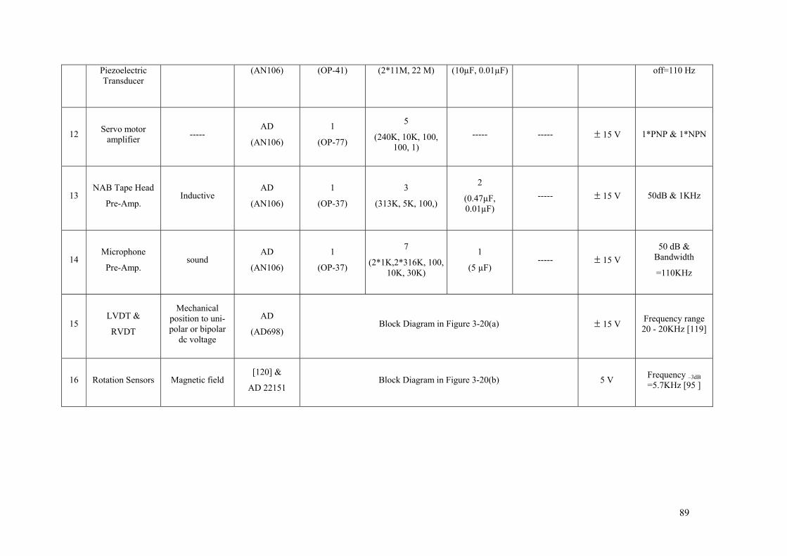
89
Piezoelectric Transducer
(AN106) (OP-41) (2*11M, 22 M) (10µF, 0.01µF) off=110 Hz
12
Servo motor amplifier
----- AD
(AN106)
1
(OP-77)
5
(240K, 10K, 100, 100, 1)
----- ----- ± 15 V 1*PNP & 1*NPN
13
NAB Tape Head
Pre-Amp.
Inductive AD
(AN106)
1
(OP-37)
3
(313K, 5K, 100,)
2
(0.47µF, 0.01µF)
----- ± 15 V 50dB & 1KHz
14
Microphone
Pre-Amp.
sound AD
(AN106)
1
(OP-37)
7
(2*1K,2*316K, 100, 10K, 30K)
1
(5 µF) ----- ± 15 V
50 dB & Bandwidth
=110KHz
15
LVDT &
RVDT
Mechanical position to uni-polar or bipolar
dc voltage
AD
(AD698) Block Diagram in Figure 3-20(a) ± 15 V Frequency range
20 - 20KHz [119]
16
Rotation Sensors
Magnetic field [120] &
AD 22151 Block Diagram in Figure 3-20(b) 5 V Frequency –3dB
=5.7KHz [95 ]

3 Sensor Application Circuits Survey for Resource Distillation
90
Table 3-3: Specifications for various operational amplifiers used in sensor interface
S.Nr Key OPA
Specification OPA335 OP291 LTC2053 LMC6001 AD8555 AD745 OP-77 OP-37
1 Open loop Gain in dB 130 85 ----- 105-135 ----- 60-72 ----- 120
2 GBW in MHz 2 3 200kHz 1.3 2 20 0.6 45-63
3 PM in ° ----- 45 ----- 50 ----- ----- ----- 72
4 Offset in µV 5 (80µ-1m)V ± 10 2000 10 100-500 25 30-100
5 Slew Rate in V/µSec 1.6 0.4 0.2 0.8 1.2 12.5 0.3 17
6 Settling Time in µSec ----- 22 ----- ----- 8 5 ----- -----
7 CMRR in dB 130 90 116 63-72 80-92 80-102 (0.1-1) µV/V 100-120
8 PSRR in dB ----- 110 116 63-80 109-125 ----- (0.7-3)µV/V (2-20)µV/V
9 Output voltage swing in V (50-100)m ----- 2.98 4.75 ----- ----- ± 14 ± 13.5
10 Input CMR in V ----- ----- ----- ----- 0.6-3.8 ± 20 ----- -----
11 Quiescent Current 350 µA ----- ----- ----- ----- ----- ----- -----

91
4. Architecture of Generic Intelligent and Adaptive Sensor System
4.1 Architecture of Target Self-x Sensor Systems
Today, industrial and consumer technical products require more and more of sensor systems. In general, smart sensors systems are equipped with sensing elements, and also with electronics needed for accurate signal conditioning. The signal conditioning includes accurate detection of the sensor signals as well as processing for further communication with computers and microcontrollers. An important feature of such sensor systems is that they are flexible and easy to use. Since the rate at which novel and new sensor products coming to market and usage are tremendously increasing. But unfortunately, only a few types of smart and intelligent sensors systems exist as market products. At present the development of sensor interface electronics is still a challenging task, which needs special know-how and experience in a multi-disciplinary field of electronics, physics, mechanics etc. However, for the front end communication from sensors to the interface electronics, no standards/general interface electronics for all sensors are available. Therefore optimization of the sensor electronics for the numerous types of electrical signals and sensor characteristics e.g., V, I, C, R, L based-inputs, requires dedicated designs for each of the particular sensor elements. As a result, in spite of the huge industrial interest, the development of sensor systems progresses rather slowly. For example, QuantumX [87] is a discrete product available in the automation market which uses several dedicated types of conditioning for the various sensor type signals.
Figure 4-1: Functional block diagram of our target generic integrated smart or intelligent self-x sensor system

4 Architecture of Generic Intelligent and Adaptive Sensor System
92
It is in the aim of this thesis work to address and provide solutions to these problems by developing and introducing a generic, flexible, self-x sensor-interface chips, which are easy to use and can be applied for a wide variety of sensor elements, sensor systems and related products. Reliability, flexibility and re-configurability of an analog system are essential to face the challenges of rapid market changes. Figure 4-1 depicts the block diagram of the proposed Generic self-x Sensor System. The inclusion of the dynamically reconfigurable universal sensor (multi-sensor) signal conditioner to the smart sensor system is illustrated in the Figure 4-1. Realization of such an adaptive or reprogrammable sensor system is a simple and direct approach to overcome some of the hardships of the traditional calibration techniques. Here, the desired or required transfer characteristics of the system are achievable through reconfiguration patterns based on compensation to dynamic working environment of the system [128].
By including this special purpose Application Specific Integrated Circuits (ASIC) to the sensor system, inheritance of the advantages of programmable / evolvable circuits can be noticed. The scope of this thesis is concerned with the reconfigurable hardware contributing to this research. The reconfigurable environment proposed by our research group consists of three separate and dedicated modules as shown in Figure 4-1. They are as follows,
4.1.1 Assessment Unit:
This unit being in the primitive stage of research contains the necessary and essential measurement setup to evaluate the hardware performance through real measurement. In a parallel work at our research group by Tawdross et al, measurement of the hardware performance was carried out in three different ways. They are, extrinsically (simulated assessment), intrinsically (measured assessment), mix-trinsically (mixture of intrinsic and extrinsic assessments) [74].
4.1.2 Optimization Unit:
The optimization unit runs the algorithms to optimize the hardware. The applied algorithms are basically bio-inspired approaches like Genetic Algorithms (GA)/Particle Swarm Optimization (PSO) etc., inheriting the desirable properties of living organisms like the self-x properties. Tawdross et al in his work, studied and implemented the possible and best suitable evolutionary approaches in optimizing the hardware designed in our research group, namely FPMA for dynamic environmental conditions [75][76]. Unlike the approach mentioned in the [89], the optimization approach investigated by Tawdross et al are capable of learning from the past and does not start from scratch all the time.
4.1.3 Reconfigurable Analog Hardware:
The scope of this thesis is to design and implement a robust hardware platform flexible at both building block and functional block levels with rapid prototyping capabilities to support a variety of

93
sensors. Several time-continuous dynamically reconfigurable hardware consisting of established analog circuit topologies were built from common building modules (two different generations) of programmable active and passive devices were realized and were used to build various circuits.
The pitfalls and the general challenges faced by the fine grained and course grained programmable structures mentioned in the chapter 2, had given us the incentive to develop a new approach, programmable at medium granular level, called Field Programmable Medium granular mixed-signal Array. The survey and collection of the distilled components with sizing information’s had provides the necessary architecture of a generic sensor signal conditioner with the required number of building blocks in a meaningful way. In the context of this report, Field Programmable Medium granular mixed-signal Array is denoted as FPMA. (Elsewhere, FPMA is also abbreviated for field programmable mixed signal array.) More information on the issues of design and implementation of this special purpose ASIC, are discussed in the following sections.
4.1.4 On-the-Fly Calibration through Dynamic Reconfigurable Analog Interface Hardware In spite of smart sensor concepts [59], conventional calibration procedures are still applicable as the conditioning electronics are manufactured separately than the sensor themselves. Hence correction of the signal to cope with the manufacturing tolerances becomes mandatory. For example, in bridge based sensor systems, resistor trimming using laser is performed to adjust the values. This procedure is difficult to automate and hence manufacturing process becomes expensive. The signal from these sensors are again has to be processed by an interface circuits prone to variations which again might require calibration.
Using dynamically programmable analog interface electronics along with dedicated software in the loop would address the above mentioned problem. The advantage of digitally programming the conditioning circuit for calibration facilitates easy automation of the proposed approach thereby reducing the cost of calibration unlike the traditional laser approach.
4.2 Architecture of the Aspired Generic/Universal Multi-sensor Signal Conditioner Our objective is to implement a standard hardware environment where embedded smart sensors of all types are pervasive. Although these devices would range greatly in their complexity, the signal processing becomes more trivial. With regard to the aspired industrial application and based on the distilled collection of signal conditioning structure with several Op Amp, cap, res, switches etc from previous chapters and Table 3-2, determination of core set of components for realising our dynamically reconfigurable universal sensor interface ICs is carried out. Figure 4-2 shows the architecture of the aspired generic sensor interface electronics.
4.2.1 Abilities of our (aspired) Generic - “One for all” Sensor Interface Electronics
1) Static and on the fly reconfigurable sensor interface electronics according to the type (different technology) and application of the available sensors and the sensors yet to come.

4 Architecture of Generic Intelligent and Adaptive Sensor System
94
2) Integration of multiple types (based on the survey in chapter 3) of sensors like voltage, current, magnetic, capacitive, and inductive based could be directly coupled to the aspired signal conditioning electronics which should cover the specification ranges specified in Table 3-3, in order to support signal conditioning of various sensors listed in Table 3-2.
3) Relief from optimization of the sensor electronics for the numerous types of sensor signals and its characteristics as they require dedicated designs for each of the particular sensor elements. “One for all” concept is applicable.
4) Time continuous and time discrete circuit realization.
5) Strong inversion and potentially weak inversion / moderate inversion circuit operations.
6) Differential to single ended and fully differential design realization
7) Repeated dynamic calibration through reconfiguration.
Figure 4-2: Architecture of the aspired “One for all” sensor interface

95
Some of the main research objectives proposed in this thesis are listed below.
1. First and foremost is to create a dynamically reconfigurable Analog Hardware Platform with programmable active and passive devices suitable for the above discussed problems.
2. To identify and bring applicable features of Evolvable Hardware from basic research to industry applications especially to sensor systems
3. Designing medium level granular approach allowing transistor level, block level and hierarchical level of reconfiguration of selected analog circuit structure based on the survey. CMOS switch assist in programming.
4. Developing a hardware platform supporting rapid prototyping (like the digital counterpart namely FPGA, PLD’s) with less switching resources and appropriate granularity for the required frequency behavior,
5. To implement circuit topologies to yield predictable behavior/reliable performances acceptable by industries.
6. No more black box structure, but instead transparent circuit structures
7. HW capable to evolve and adapt to drifts and deviations (static and dynamic), when combined with a dedicated evolutionary or organic computing techniques to exhibit self-x properties.
4.3 Devices in CMOS Technology
In the last 3-4 decades CMOS process has emerged as a most predominantly used technology. MOS transistors had become the medium of modern micro/nano electronics. It had crossed the milestone of several processes with scaling feature size. CMOS technology is the today’s only technology which provides high integration density with very low static power consumption.
4.3.1 Transistors
In CMOS process, transistors come in two forms NMOS (n-channel) transistors and its complementary PMOS (p-channel) transistors. Transistors are commonly used to amplify signal or serve as switches. Transistors can also be used to represent other devices like diode, capacitor and MOS-varactor. Conventional way of representing transistors as diode and capacitor are denoted in Figure 4-3. It is also customary to use MOS devices for realizing resistors by putting them in the ohmic region The MOS resistors occupy less area compared to the traditional POLY realization.

4 Architecture of Generic Intelligent and Adaptive Sensor System
96
Figure 4-3: Various representation of transistors a) NMOS transistor b) as diode c) as capacitor
4.3.2 Resistors
Resistors are components providing controlled amount of electrical resistance. They are used in wide variety of applications, like current limiting, voltage division, as feedback components for amplifiers, filters etc. Most technology providers offer several resistor realization materials based on the values of the resistors to be implemented. Some materials are better for manufacturing large resistors and some for low value resistors providing better accuracy and linearity. Resistors are often realized as strips of poly-silicon. Figure 4-4(a) shows the top view of a simple poly-strip resistor constructed from a homogeneous material having resistivity (ρ). If the poly-strip has a length of L µm, width of W µm and thickness of t µm, then the resistance of the poly-strip is denoted as shown in Equation 4-1. In CMOS process, it is customary to have constant thickness, hence the resistivity of the material combining with the thickness gives a new term called sheet resistance Rs normally expressed as KΩ/ .
a) b)
Figure 4-4: Resistor realization a) poly strip resistor b) typical matched resistors with dummy structures

97
Typical sheet resistance values of materials used to realize resistor are few Ω/ for poly2 and in the range of few KΩ/ for high resistive poly.
tWLR*
ρ=
Therefore, WLRsR = where, Rs (sheet resistance) = t
ρ
Equation 4-1
4.3.3 Capacitors
Capacitor is a circuit device used to store charge temporarily. It consists of two parallel plates with an insulating material in between them called the dielectric. The value of capacitor implemented in a simple parallel plate arrangement is proportional to the area of the electrodes, and to the dielectric constant. The capacitance value increases for reduced dielectric thickness. A simple implementation of an integrated capacitor is shown in Figure 4-5(a).
a) b)
Figure 4-5: Capacitor realization a) parallel plate capacitor b) matched capacitors dummy structures
4.3.4 Matching of Resistor and Capacitors
In integrated circuits, resistors and capacitors realized have a manufacturing tolerance of about ± 20%. The mismatches are caused due to the variations in the manufacturing flow like doping, oxide thickness, unnecessary etching and other process which influences the component values.

4 Architecture of Generic Intelligent and Adaptive Sensor System
98
Nevertheless, this is not an obstacle in achieving high accuracy in the design performance through precise matching. What matters in most analog design are not the absolute values of the resistors/ capacitors themselves, but the ratios of the corresponding resistor and capacitor. For example, in an inverting amplifier configuration explained in section 3.2.1, gain depends on the ratio of the resistor used in feedback. Hence precise matching is essential to attain accurate performance of analog integrated circuits, where the variations are compensated with each other in the ratio. Figure 4-4 (b) and Figure 4-5 (b) shows matched unit resistors and capacitors respectively with protective dummy structures. Laser trimming of thin film resistor can achieve tolerances of better than ± 0.1 %, but only at the cost of extra processing steps.
4.4 First Generation Programmable Basic Building Blocks
4.4.1 Programmable Transistors Array
The idea of using programmable transistor is to provide flexibility with transistor dimensions in analog circuit design while maintaining signal integrity. Flexibility in any design does not come for free; therefore a sacrificing die area is required. The proportional factors of flexibility and silicon area must therefore be traded-off against each other. In this proposed work, the gate length of the transistors are kept to be 1µm (approximately 3 time the minimum feature size of the technology used to have low channel length modulation effects, λ ) and gate widths are flexible which can take values from 1µm up to 258µm for both NMOS and PMOS transistor cells. Redundancy of the minimum sized transistors is provided three times to eliminate possible mismatching problems. Figure 4-6 shows the schematic and layout representation of scalable version of transistors with transmission gate switches.
The choice of flexibility with constant gate length was based on the fact that, any analog circuit can be implemented by just varying the width of the transistors constituting the circuit. However, the choice is dependent on the technology used. The described programmable transistors can then be used in a matrix to construct any analog circuits. Depending on the complexity of the circuit topology, number of programmable transistor used and the area consumed will vary proportionally. The total value that the scalable version of active devices can realize with its corresponding bit relations are furnished in Table 4-1.
4.4.2 Programmable Resistors and Capacitors
In most of analog circuit design, active elements alone are not sufficient, resistors and capacitors are also essential. Most area consuming components of VLSI design are also these passive components both capacitor and resistors. The tremendous use of these devices is discussed in chapter 3. Hence these components are essential for our programmable analog approach. Reconfigurable /programmable chips in general are devices whose internal connections can be varied by the users

99
Figure 4-6: Basic programmable active devices
(a) (b)
Figure 4-7: Basic programmable passive devices (a) scalable capacitor (b) scalable resistor

4 Architecture of Generic Intelligent and Adaptive Sensor System
100
in field. Programmability can be performed one time or repeatedly. In this thesis, we pursue on the fly repeated reconfiguration approach with the aid of programmable electronic switch. Figure 4-7 shows the representation of the programmable passive elements. The total value that the scalable version of passive devices can realize with its corresponding bit relations are furnished in Table 4-1. In CMOS integrated circuits, it is also customary to use active device in replacement for resistor poly strips to minimize the design area. In such realization, exhibited linearity is very important [94].
4.4.3 Switches in Programmable Analog Devices
Field programmable analog devices are not a very new idea, and various architectures realized are investigated in chapter 2. The architecture of such system is largely determined by the type of programmable interconnection technology, and the configuration storage technology. Most techniques uses CMOS processes and are therefore limited to MOS switches for the programmable interconnect, and the configurations patterns are stored in a variety of storage devices ranging from shift registers, SRAM, and EEPROM. Some more types of interconnect used are provided in the Table 2-1 and Table 4-2.
Table 4-1: First generation of basic building blocks
Nr
Programmable
Devices Symbols of
Scalable DevicesRange of Aspect
Ratios & Values
Bit
Resolution
Selection
Logic H/W
1
ST_NMOS1 W = 1 µm to 258µm
& L = 1 µm
11 Programmable
bits "1"
2
ST_PMOS1 W = 1 µm to 258µm
& L = 1 µm
11 Programmable
bits "1"
3
Scal_Res1 R = 125 Ω to 31.875 KΩ
8 Programmable
bits "0"
4
Scal_Cap1 C = 125 fF to 31.875 pF
9 Programmable
bits "1"
Firs
t Gen
erat
ion
H/W
Impl
emen
tatio
n- F
PMA
1/FP
MA
1B
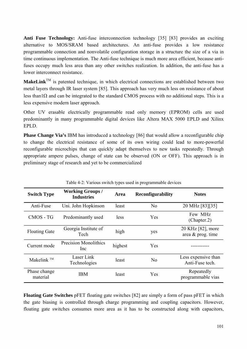
101
Anti Fuse Technology: Anti-fuse interconnection technology [35] [83] provides an exciting alternative to MOS/SRAM based architectures. An anti-fuse provides a low resistance programmable connection and nonvolatile configuration storage in a structure the size of a via in time continuous implementation. The Anti-fuse technique is much more area efficient, because anti-fuses occupy much less area than any other switches realization. In addition, the anti-fuse has a lower interconnect resistance.
MakeLinkTM is patented technique, in which electrical connections are established between two metal layers through IR laser system [85]. This approach has very much less on resistance of about less than1Ω and can be integrated to the standard CMOS process with no additional steps. This is a less expensive modern laser approach.
Other UV erasable electrically programmable read only memory (EPROM) cells are used predominantly in many programmable digital devices like Altera MAX 5000 EPLD and Xilinx EPLD.
Phase Change Via’s IBM has introduced a technology [86] that would allow a reconfigurable chip to change the electrical resistance of some of its own wiring could lead to more-powerful reconfigurable microchips that can quickly adapt themselves to new tasks repeatedly. Through appropriate ampere pulses, change of state can be observed (ON or OFF). This approach is in preliminary stage of research and yet to be commercialized
Table 4-2: Various switch types used in programmable devices
Switch Type Working Groups / Industries Area Reconfigurability Notes
Anti-Fuse Uni. John Hopkinson least No 20 MHz [83][35]
CMOS - TG Predominantly used less Yes Few MHz (Chapter.2)
Floating Gate Georgia Institute of Tech high yes 20 KHz [82], more
area & prog. time
Current mode Precision Monolithics Inc highest Yes -----------
Makelink TM Laser Link Technologies least No Less expensive than
Anti-Fuse tech.
Phase change material IBM least Yes Repeatedly
programmable vias
Floating Gate Switches pFET floating gate switches [82] are simply a form of pass pFET in which the gate biasing is controlled through charge programming and coupling capacitors. However, floating gate switches consumes more area as it has to be constructed along with capacitors,

4 Architecture of Generic Intelligent and Adaptive Sensor System
102
typically in a CPOLY implementation. Programming a floating gate transistor or a switch is a tedious time consuming task.
Transmission Gate Switches: In CMOS process, NMOS and PMOS transistors are connected in parallel to contribute electronic switch. The schematic representing of the predominantly used (in the context of field programmable analog devices) Transmission Gate (TG) switch is shown in Figure 4-8. An ideal switch is a component, when conducting between two nodes establishes a connection without voltage drop across them with currents flowing in both directions. When the switch is open, then the two nodes to which the switch is connected totally becomes isolated. This type of switches on the contrary to a single MOS switches have less voltage drop across them, have high dynamic range and since n-channel and p-channel devices are connected in parallel and requires opposite clocks, the feed through due to the clocks will be minimized through cancellation. In reality, CMOS switches are non-ideal. Every electronic component has its internal capacitance (parasitics) which limit the frequency behavior of that particular component.
In case of analog circuit like amplifiers, parasitic capacitances have tremendous impact on the frequency behavior. But in the case of logic applications, these capacitances limit the speed of the circuits. Figure 4-9 shows the graphical representation of various capacitances associated with the MOS field effect transistors, namely NMOS transistor in which a resistive channel region connects the source and drain.
)('
1
VthVgsL
WnKRon
−= in Ω
Equation 4-2
Figure 4-8: Transmission gate switch and its equivalent circuit when closed (Top) when open (Bottom)

103
In the case of transmission gate switches, parasitic capacitances and on resistance properties remains vital for consideration in the operation of the whole circuit in which the switches are deployed. CMOS transmission gate switches have more parasitic than the single channel switches, hence dimensioning the TG switches is important for ON resistance and parasitic capacitances. State of the art of silicon switch design and manufacturing technologies have no choice to have less on-resistance and less parasitic capacitance at the same time with respect to the area consumed. The on resistance of MOS transistors can be given as shown in Equation 4-2. A comparison of different switch implementation and its characteristics [KPBS] is shown in Table 4-3. It can be noted from the table that the on resistance of the CMOS switch is higher than the low resistive relays enjoyed once upon. On the other hand CMOS approaches require very less area and are several times faster than the mechanical counterpart.
Breaking the bottleneck: The limitations inferred in the frequency behavior, due to the use of various types of switching resources, in various programmable devices as listed in Table 4-2 can be minimized. From the Equation 4-2, we understand that the on resistance of the switches can be
Table 4-3: Comparison of various switches (from [KPBS]).
S.Nr Parameter Mechanical Relays CMOS Switch
(0.35µm)
Bipolar Switch
(0.35µm)
1 On-Resistance 10-2 Ω 102 to 103 Ω -------
2 Off-Resistance 1012 Ω 1012 Ω 1010 Ω
3 Conduction Direction Bidirectional Bidirectional Unidirectional
4 Switching time ≥ 500µseconds <1 µseconds < 1 µseconds
minimized by the increasing the gate source voltage (Vgs) of the transistors constituting the switches. Increasing the Vgs results in less on resistance, hence during the design phase small area consuming switches can be realized with less on resistance and less parasitic capacitances. Two different ways of boosting the Vgs are given below,
1. Charge pump is an established design procedure to boost voltage levels.
2. Use of separate supply voltages for analog and digital and with enhanced Vdd for digital domain thereby the output of the digital logic’s are lifted to comparatively high voltage level.
Here care should be taken that boosted gate voltage feeding in to the transistors should be below the breakdown voltage of the transistor. In our case, 5.0V is the maximum voltage a transistor can withstand. Figure 4-10 shows the range of on resistance exhibited by the TG switches for the dimensions used (W=nmos/pmos=0.6µm/1.9µm for L=0.35µm) in various hardware realization. On the average, on resistance of TG in FPMA1 is 3.9 KΩ for Vgs=3.3 V and is 3.1KΩ for Vgs=4.8 V.

4 Architecture of Generic Intelligent and Adaptive Sensor System
104
Figure 4-9: Capacitances associated with NMOS transistor cross sectional view (left) 3-D view (right)
(a) Switch of FPMA1 (b) Switch of GOPA
Figure 4-10: ON – resistance of transmission gate CMOS switches
4.4.4 Shift Register for Sequential Device Selection
A Shift Register is realized of number of single bit "D-Type" latches in master slave arrangement connected together in a chain arrangement so that the output from one becomes the input of the next and so on, thereby shifting the stored data serially from one direction to the other. The number of individual D-type latches used to construct a shift register depends on the number of bits to be stored. From the Table 4-1 in section 4.4.3, we require shift registers of bits 11, 9 and 8 for each scalable versions of transistor, capacitor and resistor respectively in our first hardware realization. These numbers are slightly varied for the other implemented hardware and will be explained in the

105
upcoming sections. Shift registers are used to store data and to convert data from a serial to parallel or parallel to serial format with all the latches being driven by a common gated clock signal.
Figure 4-11: Master Slave Arrangement of D-Flip Flop
Figure 4-12: 11 bit shift register with two phase clock
The structure used in our work is a master slave arrangement with two phase clock arrangement (φ1 and φ2) as shown in Figure 4-11 [2]. Figure 4-12 show a shift register of 11 bits. Assume that all the flip-flops (1 to 11) have just been RESET through logic “0” and that all the outputs (Q1 to Q11) are at logic level "0". If a logic "1" is given to the data input pin of flip flop1 then on the first clock pulse the output of flip flop 1 (Q1) will be set HIGH to logic "1" with all the other outputs remaining LOW at logic "0". Assume now that the data input pin of 1 has returned LOW to logic

4 Architecture of Generic Intelligent and Adaptive Sensor System
106
"0". The next clock pulse will change the output of 1 to logic "0" and the output of Q2 is HIGH to logic "1". The logic "1" has moved or been "shifted" one place along the register to the right. When the third clock pulse arrives the logic "1" moves to the output of 3 (Q3) and so on until 11 clock pulse which sets all the outputs Q1 to Q11 to logic level "0" because the input has remained at a constant logic level "0". The effect of each clock pulse is to shift the data (D) contents of each stage one place to the right, until the complete data is stored, which can now be read directly from the outputs Q1 to Q11. Here it can be seen that the data D has been converted from a serial data signal to a parallel data signal. The output data from Q1 –Q11 are not directly given to the analog array to choose the components from the array, but instead, a protective logic is introduced in between. The output data now becomes along with the function of an additional protective signal called Enable (EN) as shown in Figure 4-13. The truth table for the logic used is also depicted. The enable signal provides isolation of the digital circuits from the analog while in operation.
Figure 4-13: 11 bit shift register with protective logic
The number of clock pulse required to store data in shift registers constituting each of the scalable active and passive devices are, for Scalable Transistor = 11 clock pulses, Scalable Capacitor = 9 clock pulses, and Scalable Resistor = 8 clock pulses. The mixed signal, scalable block of NMOS transistor are shown in Figure 4-14. The placement of the digital cells (shift registers) surrounding the analog array was preferred to save area. In-spite of the protective logic for isolation of the two

107
domains as discussed in previous section is used, placement of the cells, routing the power lines are also crucial. In mixed-signal, along with the effects like unwanted voltage drops and electro-migration, noise considerations should also be taken into account. Tremendous switching activities in mixed signal design instantiate transient spikes in the circuits hampering the behaviour of the analog circuit. More details about noise are discussed in section 4.7.5.
Figure 4-14: Mixed signal Scalable NMOS transistor array with shift register and its equivalent layout
Table 4-4: Area comparison of various programmable building blocks
S. Nr Devices Description Area 1 ST_NMOS Scalable NMOS transistor array 64 µm * 60 µm 2 ST_NMOS_SR Scalable NMOS transistor array with shift register 115 µm * 115 µm 3 ST_PMOS Scalable PMOS transistor array 65 µm * 69 µm 4 ST_PMOS_SR Scalable PMOS transistor array with shift register 116 µm * 120 µm 5 Scal_Cap Scalable capacitor array 231 µm * 211 µm
6 Scal_Cap_SR Scalable capacitor array with shift register (245µm*215µm)+(18µm*157µm)
7 Scal_Res Scalable resistor array 23 µm * 209 µm 8 Scal_Res_SR Scalable capacitor array with shift register 55 µm * 213 µm

4 Architecture of Generic Intelligent and Adaptive Sensor System
108
4.4.5 Comparison of Area Requirement with 6T-SRAM Cell.
The 6T SRAM cell shown in the Figure 4-15(a) is the most commonly used in commercial chips. In this static memory structure the data is stored in the cross coupled inverters. An alternative scalable version of the NMOS transistor with random accessing scheme is shown in Figure 4-15(b). A case study was carried out to estimate the area requirement between the two accessibility approaches. Like the sequential approach, random accessible approach is also provided with the protective logic to isolate the digital and analog domain. The area consumed only by the scalable array by random approach was comparatively less but was increased when implemented along with the address decoders for the SRAM cells. Hence for small complexity circuits shift registers are preferred. But nevertheless, for more complex structures RAM can be preferred.
4.4.6 CMOS Operational Amplifiers
Operational amplifiers (Op Amps) are very important building blocks in analog circuit design. Op Amps have sufficiently large open loop gain, closed loop negative feedbacks are provided to stabilize the transfer function independent of the gain of Op Amp. Most of the Op Amps do not have high open loop gain, hence additional gain stages are added to the Op Amps. Another desired parameter is the low-offset. For op amp offset, large transistor size for the input differential pair may be used. With layout design techniques such as inter-digitations and common-centroid structure, offset can be reduced. Alternatively, auto zeroing or chopper stabilization techniques can be employed. In this section different amplifier topology with varying complexity are investigated by replacing the unit devices with the scalable active and passive devices.
(a) (b) Figure 4-15: 11 bit programmable transistor array with SRAM

109
4.4.6.1 Miller Operational Amplifier
One of the simple and an established two stage structure is taken for our initial investigations as it supports internal compensation schemes. Stability in Op Amp circuits is crucial as it impacts the frequency behavior and the settling time of the circuit. In this chapter, along with the simple two stage Miller amplifier structure, more complex Folded Cascode (FC) operation amplifiers are initially investigated for flexibility which has better performance than the two stage structure like for example better rejection ratio’s, input common mode range, etc. These building blocks are then considered to build other analog circuits like instrumentation amplifiers and fully differential amplifiers. The schematic of the two stages Miller Op Amp is shown in Figure 4-16. The circuit consists of 13 devices in total. The schematic is depicted after replacement of the unit devices (non programmable active and passive devices) with programmable devices (scalable transistors, scalable capacitors and scalable resistors). The programmable Miller Op Amp structure needs in total of 5 scalable PMOS transistor, 6 scalable NMOS transistor, 1 scalable capacitor and 1 scalable resistor [127]. Therefore the total bits required to configure the Miller amplifier topology can be calculated from Table 4-1 to be equal to 138 bits. The scalable devices, during the implementation are wired in the following sequence of selection - M10, M9, M3, M4, M5, M11, M1, M2, M8, M7, M6, R1 and Cc. This means the digital data input is first given to the scalable PMOS transistor M10 and data output are taken after Cc. The devices last in the sequence, gets configured first through the two phase gated clocking scheme. In Miller OPA structure Cc gets configured first and M10 at the last. The area consumed by the Miller Op Amp topology is given in Table 4-12. The Miller OPA structure can be made to operate as Comparator by isolating and removing the compensation capacitor (Cc) from the feedback loop. The isolation of the compensation capacitor is performed through turning off the TG switches connected to the top and bottom plates. The complete layout implementation of dynamically reconfigurable (time-continuous) Miller operational amplifier cell is shown in Figure A-1.
4.4.6.2 Selective Node Flexibility of Op Amp
In-spite of better fault tolerant capability of the above described Miller OPA, traditional analog designers remain skeptical about the area consumption. Hence various case studies are performed in which flexibility are provided only to specific nodes. The nodes given flexibility corresponds to a certain specs of the circuit. Table 4-5 [93] and Figure 4-17 illustrates the various nodes and its influencing specification. The layout of the four cells are shown in Figure 4-18 The selective node flexibility approach has to be traded off against area and fault tolerance of the circuit. The area consumed for various optimized specific nodes for Miller OPA is listed in Table 4-5. The nodes are selected based on the criterion to optimize certain important Op Amp parameters like gain, offset etc, as listed in the Table 4-5. The area consumed by this is comparably small than the complete scalable version explained in section 4.4.6.1. This approach is suitable for applications where the circuits are in conjunction with MEMS because of less overall area requirement with descent fault tolerance.

4 Architecture of Generic Intelligent and Adaptive Sensor System
110
Table 4-5: Case studies for node sensitivity [93]
S.Nr Case studies Selective Scalable Nodes
Optimization Parameter Area
1 Case study 1 M7 Speed 100 µm* 96 µm
2 Case study 2 M5 & M7 Offset 165 µm * 85 µm
3 Case study 3 M5 & M8 (Cc-turned off) Comparator 148 µm * 64µm
4 Case study 4 M8 & M6 Power Consumption 125 µm * 100 µm
Figure 4-16: Miller compensated two stage operational amplifier with scalable devices
4.4.6.3 Folded Cascode Operational Amplifier (FC_OPA)
In spite of the satisfactory performance of the above discussed two stage amplifier, improvement in the performance for high gain, better PSRR, better settling time, driving capability etc. can be preferred. Hence a modification of the above two stage structure is essential. Therefore a cascoded structure is preferred. Especially a folded cascode operational amplifier shown in Figure 4-19 is chosen as it has little larger input common mode range because of its three stacked transistor arrangement than the non folded cascoded (telescopic Op Amp) version with five stacked transistors. The schematic of the FC_OPA shown in Figure 4-19 consist of 25 scalable devices in total. Out of which, 10 are scalable PMOS transistors, 13 are scalable NMOS transistors, 1 scalable

111
capacitor and 1 scalable resistor [131]. The total bits required to configure the complete folded cascode structure can be calculated from Table 4-1 to be equal to 270 bits. The scalable devices used in realizing the folded cascode structure are wired in the following sequence of selection - M22, M21, M3, M4, M5, M8, M9, M17, M18, M23, M1, M2, M6, M10, M11, M16, M20, M19, M14, M7, M13, M12, M15, Cc and R1. The digital data input are given to M22 first and digital output is from R1. Like the Miller OPA structure explained in section 4.4.6.2, two phase gated clocks help in loading the bit patterns first starting from the last device in the mentioned sequence. This means scalable resistor R1 gets configured first and scalable transistor M22 at the last. The area consumed by the programmable folded cascode amplifier is given in Table 4-12. The layout realization is shown in Figure A-1.
(a) (b)
(c) (d)
Figure 4-17: Various case studies investigated for Miller topology for selective node flexibility based on better performances like (a) speed (b) low offset (c) low power (d) as comparator

4 Architecture of Generic Intelligent and Adaptive Sensor System
112
Figure 4-18: Miller OPA layout for selective node flexibility realized by students in their semester projects
with ST_NMOS / ST_PMOS based on Table 4-5.
4.4.7 Instrumentation Amplifier
So far, amplifier topologies with increasing complexity were investigated and implemented with basic building blocks of scalable devices. These amplifier topologies can be used as single instance and /or as multiple instances. Amplifiers combining with the other passive devices are capable of realising other useful analog circuits like filters and instrumentation amplifiers. Instrumentation amplifiers are the most common signal conditioning device used in several applications like data acquisition systems and motor control. An instrumentation amplifier is a structure with inbuilt closed loop gain. The topology has a differential input and single ended output. The detailed circuit topology of a typical 3 Op Amp, 7 resistor instrumentation amplifier (In Amp) is shown in Figure 4-20(a). The structure has 2 buffer amplifiers, one at each input and the third amplifier arranged in as a subtractor. The amplifiers used to realize instrumentation amplifier are the folded cascode operational amplifiers explained in section 4.4.6.3. The total bits required to configure the In Amp therefore becomes 1258 bits.

113
Figure 4-19: Folded cascode operational amplifier with scalable devices
The sequence of the digital data is given to OPA1 and then to OPA2, OPA3, R3, R4, R5, R6, R7, R8 and finally the data output is taken from R9. The output equation of the In Amp is given in Equation 4-3. Here, R3=R5, R6=R8 and R7=R9. Hence by choosing appropriate resistor values from our scalable range desired gain can be obtained.
)21)(4321(
89 VinVin
RR
RRVout −+= Equation 4-3
In order to obtain more closed loop gain, several scalable resistors are connected in series to realize big resistors. Eight scalable resistors are connected in series to obtain a single large resistor of value 255 KΩ (8*31.875KΩ). Figure 4-20(b) shows a typical bridge sensor application of the instrumentation amplifier used to test the In Amp. While sensing a signal, the bridge sensor resistor values changes, imbalance in the bridge causes a differential output voltage across the bridge. The differential output voltage coming out of the sensor bridge is given directly to the inputs of the In Amp. A dc voltage equal to the common mode voltage is also applied on both inputs. The layout of In Amp is shown in Figure A-1.

4 Architecture of Generic Intelligent and Adaptive Sensor System
114
(a) (b)
(c)
Figure 4-20: (a) Instrumentation amplifier with scalable devices (b) performance evaluation of In Amp with typical resistive bridge sensor (c) Extrinsic transient response of In Amp.
4.5 Generic OPerational Amplifier – “GOPA”
In this section we focus on building a special generic amplifier block which is flexible to both dimensions and topology. Generic OPerational Amplifier (GOPA) consists of array of scalable active and passive devices. The next level hierarchical switches called Topology Switches (TS) interconnect the heterogeneous arrays. Transmission gate switches constitute the topology switches. By switching ON and OFF these topology switches interconnecting the scalable array, various established amplifier topologies are realized ranging from a simple Miller to Telescopic operational amplifier. The flexibility is not only restricted to two stages but are also extended to three stage amplifier structures with programmable compensation capacitors and nullifying resistors. Some possible building structures of any operational amplifier topology that are realized by GOPA are simple and cascoded current mirrors, Wilson current mirror in the tail current region. Diode or

115
current mirror loaded differential pairs and cascoded output stages. Realization of single ended and differentially ended output is also realized [125].
Figure 4-21: Hierarchy of analog circuits from GOPA
The GOPA structure is capable of realizing more than 15 established simulation verified amplifier structures (see Figure 4-21 for the various realizable structures) providing complete flexibility both in the choice of the structure and in sizing the devices constituting the structures. Combination of several stages mentioned in Figure 4-21 with scalable active and passive devices constitutes GOPA. Figure A-3 shows the physical implementation of the sensor signal amplifier realized from GOPA constructed with the scalable devices. The layout consist a total of 45 scalable devices and 59 topological switches. In this work, simulations were carried out in the so called extrinsic fashion. A considerable degree of behavior comparability is to be expected with the manufactured chip of the dynamic re-configurable folded cascode operational amplifier performed later with intrinsic simulations. With regard to practical applications, in addition to normal pins of the Op Amp, data (D) pin, enable (EN) pin, clock (clk) pin are essential. The enable signal ensures that the digital section does not interact with operation phase of the amplifier after suitable device selections are performed. This ensures additional separation between the different domains of analog and digital is not necessary. The objective of this chip comes after studying the need and advancement in the field
4 Architecture of Generic Intelligent and Adaptive Sensor System
116
of measurement and instrumentation. Our design objective is to create cells of clear compatibility to that of the industrial standards with expectable behavior along with incorporation of existing design knowledge. The chip can be used in as a single or multiple instances. Nevertheless, this area greedy approach can’t be justified for manufacturing due to enormous area expense. However the approach consumes less area compared to the FPTA approach.
4.5.1 Hierarchical Switches/Topological Switches
The next level of switches used to construct different amplifier circuit topologies is called Topology Switches (TS). TS switches are also transmission gate switches. The dimensions of the TS are NMOS/PMOS, W=0.9µm/2.85µm with L= 0.35µm in both transistors. The ON resistance of these switches on an average is 2.675KΩ for Vgs=3.3 V applied to the gates of the NMOS constituting the TS. The ON resistance is reduced to 2.11KΩ by boosting the gate voltage to 4.8 V.
4.5.2 Various Amplifier Structure
One of the most important requirements of Op Amp is large gain. To obtain larger gain Op Amp, several amplifier stages can be connected together. The choice made from these available stages and the manner in which they are wired to each other determines the topology of the amplifier circuits. In general, the input stages of the Op Amp are concerned with aspects like bias, offset, common mode rejection, and input range. Output stages are concerned with power, compensation in feedback or feed-forward. The rest of the aspects of Op Amp like gain, frequency response, slew rate and linearity are concerned with the amplifier as whole including input stage, intermediate stage and output stage. Intermediate stage is connected between the input stage and the output stage. Figure 4-21, shows the possible stages, compensations, and protection schemes which can be realized through GOPA. Figure 4-22 and Figure 4-23 shows schematics of some possible amplifier stages. Care should be taken in selecting the stages from the possibilities. For example, when Wilson biasing combined with telescopic amplifier arrangement (input stage), there are 6 stacked transistors at the input stage which would give a reduced input common mode range. The special generic amplifier hardware when combined with the optimizing software adapts to the topology according to the specification requirement. Figure 4-24 and Table 4-6 shows amplifier performances for miller and folded cascode topologies realized through GOPA.
4.6 Low Power Design
Continued voltage scaling and technology shrinking has positive influence on power consumption as far as digital circuits are concerned as the power consumptions is a function of applied voltage.

117
(a) (b)
(c) (d)
Figure 4-22: Various circuit realisations from GOPA

4 Architecture of Generic Intelligent and Adaptive Sensor System
118
Figure 4-24 shows the roadmap of future technologies implying reduction in the applied voltage. But whereas in analog signal processing, voltage scaling has negative influence as the applied voltage is proportional to dynamic range and linearity. Low power trends are important for various reasons, like circuits being used in battery powered applications, mobile applications and to minimize power dissipation of the circuit. Like the other performance parameters of any analog circuit, power is also a vital trade off criterion.
(a) (b)
Figure 4-23: Various circuit realisations from GOPA continued
Figure 4-24: Bode diagram of Miller OPA realized from GOPA

119
Table 4-6: Specs of FC OPA realized from GOPA for different switching voltages
S.Nr GOPA
(FC OPA)
Switch Voltage nmos=3.3V
& pmos=0 V Switch Voltage nmos=5V
& pmos=0V 1 Gain 92.2dB 91.3dB
2 Phase Margin 61.2° 68°
3 Gain Band Width 1.43MHz 1.118MHz
4 Offset 0.36mV 0.37mV
5 Input CMR 1.78V 1.73V
6 Slew Rate 5.1V/µSec 4.66V/µSec
7 Settling time 2.5µSec 2.05µSec
8 CMRR 58dB 59dB
Figure 4-25: 2007 ITRS half pitch and gate length [ITRS]
4.6.1 Low Power Configurations
Shrinking the devices and reducing the supply voltage accordingly, will not degrade voltage gain in the case of amplifiers. Nevertheless, scaling down the dimensions while maintaining the supply voltage constant will however decrease the gain. Thermal noise will remain constant because the

4 Architecture of Generic Intelligent and Adaptive Sensor System
120
device transconductance remains constant under constant field scaling. The 1/f noise intensifies, but the effect of this can be reduced by using chopper stabilization. Biasing the transistor for very low current causes the operating region of the transistors in weak inversion, moderate inversion and strong inversion regions. The power consumption of the Op Amps can be minimized by the use of architecture with only a single (differential) stage. This will reduce the power consumption of the device. However, better gain, acceptable bandwidth and slew rate etc are also essential. Hence an output stage can be added to fulfill the requirements. Appropriate optimizing the biasing circuits will reduce the power consumption in Op Amps. Quiescent power dissipation in Op Amps can be reduced by appropriate choice of the amplifier topology. Two stages Miller Op Amp shown in Figure 4-16 and Folded cascode Op Amp shown in Figure 4-18 are investigated and configured for various power requirements as shown in Figure 4-25. The knowledge of the minimum possible power requirement from these cells will be useful to another power saving technique called as “soft sleep”. More information regarding this “soft sleep” power saving procedures is explained in section 4.7.4.5.
(a) (b)
(c) (d)
Figure 4-26: Frequency behaviour of Miller OPA (a), (b) & Folded cascode OPA (c), (d) for various
power requirements
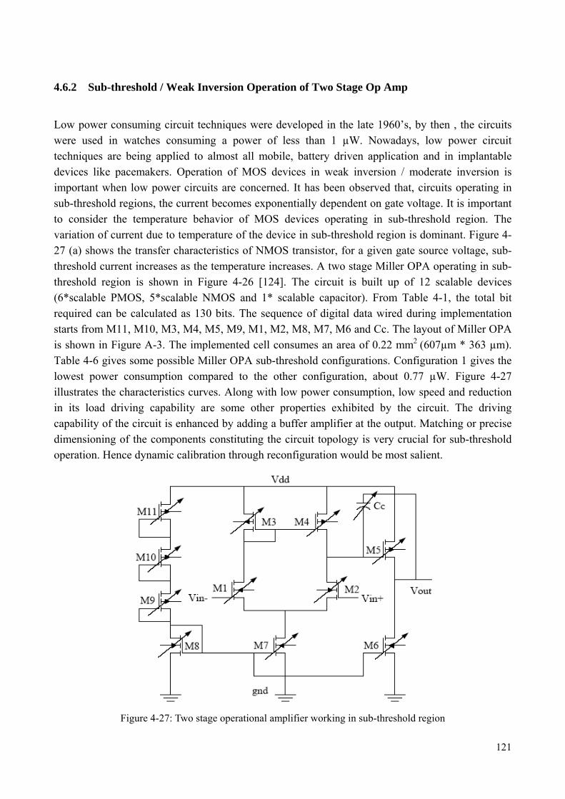
121
4.6.2 Sub-threshold / Weak Inversion Operation of Two Stage Op Amp
Low power consuming circuit techniques were developed in the late 1960’s, by then , the circuits were used in watches consuming a power of less than 1 µW. Nowadays, low power circuit techniques are being applied to almost all mobile, battery driven application and in implantable devices like pacemakers. Operation of MOS devices in weak inversion / moderate inversion is important when low power circuits are concerned. It has been observed that, circuits operating in sub-threshold regions, the current becomes exponentially dependent on gate voltage. It is important to consider the temperature behavior of MOS devices operating in sub-threshold region. The variation of current due to temperature of the device in sub-threshold region is dominant. Figure 4-27 (a) shows the transfer characteristics of NMOS transistor, for a given gate source voltage, sub-threshold current increases as the temperature increases. A two stage Miller OPA operating in sub-threshold region is shown in Figure 4-26 [124]. The circuit is built up of 12 scalable devices (6*scalable PMOS, 5*scalable NMOS and 1* scalable capacitor). From Table 4-1, the total bit required can be calculated as 130 bits. The sequence of digital data wired during implementation starts from M11, M10, M3, M4, M5, M9, M1, M2, M8, M7, M6 and Cc. The layout of Miller OPA is shown in Figure A-3. The implemented cell consumes an area of 0.22 mm2 (607µm * 363 µm). Table 4-6 gives some possible Miller OPA sub-threshold configurations. Configuration 1 gives the lowest power consumption compared to the other configuration, about 0.77 µW. Figure 4-27 illustrates the characteristics curves. Along with low power consumption, low speed and reduction in its load driving capability are some other properties exhibited by the circuit. The driving capability of the circuit is enhanced by adding a buffer amplifier at the output. Matching or precise dimensioning of the components constituting the circuit topology is very crucial for sub-threshold operation. Hence dynamic calibration through reconfiguration would be most salient.
Figure 4-27: Two stage operational amplifier working in sub-threshold region

4 Architecture of Generic Intelligent and Adaptive Sensor System
122
Table 4-7: Some Miller OPA sub-threshold configuration
Device Dimensions in µm
Con
figur
atio
n
M1 M2 M3 M4 M5 M6 M7 M8 M9 M10 M11Cc
(pF)
Power
(µW)
Gain
(dB)
PM
(Deg)
GBW
(KHz)
1 24 24 128 128 256 16 16 72 28 28 28 16 3.46 88 58 51
2 128 128 128 128 256 4 4 32 32 32 32 24 1.92 91 60 55
3 44 44 36 36 70 24 24 256 16 16 16 16 1 90 56 45
4 44 44 36 36 70 24 24 192 4 4 4 16 0.4 84 58 19
(a) (b)
(c) (d)
Figure 4-28: NMOS with long channel (L=10µm) transfer characteristics for various temperatures (a) characteristics for Miller OPA in sub-threshold operation (b) (c) (d)

123
4.7 Second Generation Programmable Basic Building Blocks
4.7.1 Programmable Active and Passive Devices
The second generation of scalable active and passive devices has small modifications added to its structure compared to its predecessor. The value and symbol notation of the second generation programmable devices are furnished in Table 4-8. The incentive of the second generation devices comes after understanding that, in first generation implementation, the gates of the transistors were kept floating when unselected. The dynamic range covered by the programmable transistor (both NMOS and PMOS) remains identical from a minimum width value of 1 µm to a maximum of 258 µm with 11 bit resolution. Like the first generation implementation, the lengths of the unit devices are fixed to 1 µm. Redundancy of the minimum sized transistors are provided three times to eliminate possible mismatching problems. The circuit implementation of the scalable array for NMOS and PMOS are shown in Figure 4-28 (a) [133]. It is clear from the schematic that the unselected transistors of the array are no more floating, but instead connected to ground or Vdd according to the type of transistors used.
Table 4-8: Second generation of basic building blocks
S.
Nr
Programmable
Devices Symbols of
Scalable DevicesRange of Aspect
Ratios & Values
Bit
Resolution
Selection
Logic H/W
1
ST_NMOS2 W = 1 µm to 258µm
& L = 1 µm
11 Programmable
bits "1"
2
ST_PMOS2 W = 1 µm to 258µm
& L = 1 µm
11 Programmable
bits "1"
3
Scal_Res2 R = 250 Ω to 511.750 KΩ
11 Programmable
bits "0"
4
Scal_Cap2 C = 125 fF to 31.875 pF
9 Programmable
bits "1" Se
cond
Gen
erat
ion
H/W
Impl
emen
tatio
n- F
PMA
2

4 Architecture of Generic Intelligent and Adaptive Sensor System
124
(a)
(b)
Figure 4-29: Second generation of scalable active devices

125
In case of NMOS, gate is connected to the ground and in case of PMOS the gate is given to Vdd, thereby turning off the transistors completely. The increase in the node capacitances is observed due to the circuit arrangement. Like the first generation scalable devices, selection of the devices from the array are done sequentially through shift registers as explained in section 4.4.4.
(a) (b)
Figure 4-30: Input transfer characteristic comparison of unit and programmable transistor for (a) W/L = 10/1 µm and (b) 258/1 µm
(a) (b)
Figure 4-31: Output transfer characteristic comparison of unit and programmable transistor for (a) W/L = 10/1 µm and (b) 258/1 µm

4 Architecture of Generic Intelligent and Adaptive Sensor System
126
The layout implementation of the transistor arrays are also shown in Figure 4-28(a). It is clear from dimensions denoted that the transistor array of the second generation occupies less area with enhanced protection. The input and output transfer characteristics of the scalable transistor (NMOS for example) are shown in Figure 4-29 and Figure 4-30. The different graphs show the comparison between the scalable and the unit non programmable devices for certain aspect ratios. It can be noted from the graphs that, the small deviations noticed is due to the on resistance of the TG switches used in the scalable versions of the transistor. The device with 258 µm width is chosen to understand the effect of all the TG switches being turned on in the scalable array.
Differential pair transistors Most integrated amplifiers have two inputs with opposite signs. To implement a differential input stage almost all of the amplifier structures uses a circuit arrangement called differential pair transistors. The importance of this circuit arrangement is well established. The schematic representation of such a differential pair transistors realized with the scalable transistors is shown in Figure 4-28(b). The layout implementation of such source coupled differential pair transistors is also depicted in Figure 4-28(b). The layout implementation highlights two matched transistors pair implemented through the scalable version of the transistors. Matching of transistors at the differential pair is very essential, as a small variations or mismatches would give rise to more output offset voltage. Each of transistors in the differential pair has 11 unit transistors (see Table 4-8).
Table 4-9: Area comparison of various programmable second generation building bocks
Nr Devices Description Area 1 ST_NMOS2_SR Scalable NMOS array with shift register 67 µm *43 µm 2 ST_NMOS2P_SR Scalable NMOS transistor array pair 182 µm * 97 µm 3 ST_PMOS2_SR Scalable PMOS array with shift register 67 µm * 46 µm 4 ST_PMOS2P_SR Scalable PMOS transistor array pair 182 µm * 105 µm 5 Scal_Cap2_SR Scalable capacitor array with shift register 249µm * 246µm 6 Scal_Res2_SR Scalable resistor array with shift register 246 µm * 115 µm
The parallel connected transistor have widths =1µm, 2µm, 4µm, 8µm, 16µm, 32µm, 64µm and 128µm. The total range becomes 258µm by selecting all. Here the minimum sized transistors, i.e. for W=1µm, are redundantly placed 4 times for matching reasons. Transistors from W= 1µm until W=32µm of M1 and M2 are realized with coupled source terminals in non-folded transistor fashion, whereas, W=64µm and W=128µm are source coupled in folded transistor fashion. The later transistor dimensions have better matching than the former dimensions. Just for the sake of better area requirement and easy wiring two different matching schemes were followed. However, it is better to have all the transistors with enhanced matching realization. From the optimization software point of view, the deviations originating from these mismatches are not amenable. Therefore matching techniques at the design level of evolvable chips are important. The layout implementation through matched technique also reduces some portion of silicon. The area occupied by scalable NMOS and PMOS, when implemented alone or as transistor pairs are denoted in Table 4-9.

127
(a) (b) Figure 4-32: Second generation of scalable capacitor (a) schematic representation (b) matched layout
implementation
The need for scalable passive devices for programmable analog design approaches are understood from chapter 3. In case of scalable capacitor, the range of values covered by the scalable version remains identical with its first generation. The total value that a scalable capacitor can realize is furnished in Table 4-8. The bit resolution of the structure also remains identical. The only difference in the second generation of capacitor array is the various switch dimensions optimized for on resistance and signal path bandwidth. The heterogeneous switch dimensions are followed. This means that the switches S1 to Sn in Figure 4-31(a) is not identical (For scalable capacitor n is equal to 9). The different dimensions are furnished in Table 4-10. The irregular switch dimensions are followed to have better signal path bandwidth. More details about the switches and signal path bandwidth determination will be explained in section 4.7.2. The schematic representation of scalable capacitor is shown in Figure 4-31(a) and Figure 4-31(b) represent the matched layout implementation of the circuit shown in Figure 4-31(a).The capacitors are implemented in a poly–poly parallel plate approach. The area consumed by the scalable capacitor array is given in Table 4-9.
The second generation of scalable resistors on the other hand has some modification in its values and in bit resolutions. The schematic representation of the second generation scalable resistor remains identical as shown in Figure 4-7(b). The minimum and maximum realizable values, bit resolution and selection logic of the devices from the array are given in Table 4-8. The on resistance of the TG switches used in these arrays is much reduced to be around 45Ω. The dimensions of the TG switches will be explained in the next section. The layout implementation of resistors is carried out with the use of technology specific high resistive poly material (RPOLYH). The advantage of

4 Architecture of Generic Intelligent and Adaptive Sensor System
128
using RPOLYH is to save silicon area while realizing high resistor values. RPOLYH remains suitable to realize high resistor values because of its high sheet resistance. Sheet resistance of RPOLYH in is the range of few KΩ/ . The area consumed by the second scalable resistor is given in Table 4-9.
4.7.2 Transmission Gate Switches
Circuit structure of the transmission gate switches and its operation were explained in detail in section 4.4.3.
Table 4-10: On resistance for various TG switches
Transmission Gate
Switch
ON-Resistance of
(TGmax) in Ω for
Vgpmos=0 V
ON-Resistance of
(TGmax) in Ω for
Vgpmos= -1.65V Scalable Devices
PMOS (W/L) in
µm
NMOS (W/L) in
µm
V(gnmos) =3.3V
V(gnmos) =4.8V
% ON-
Resistance
Reduction V(gnmos) =3.3V
V(gnmos) =4.8V
% ON-
Resistance
Reduction
ST_NMOS2 3.9/0.35 1/0.35 2.87 K 2.1 K 26.82 1.69 K 1.44 K 14.79
ST_PMOS2 3.9/0.35 1/0.35 2.87 K 2.1 K 26.82 1.69 K 1.44 K 14.79
Scal_Res2 150/0.35 50/0.35 57 41.5 27.19 40 32 20
Scal_Cap2
S1 5.4/0.35 1.2/0.35 2.33 K 1.73 K 25.75 1.26 K 1.19 K 5.5
S2 5.8/0.35 1.3/0.35 2.15 K 1.6 K 25.58 1.16 K 1.01 K 12.93
S3 5.5/0.35 2/0.35 1.53 K 1.12 K 26.79 1.06 K 873 17.64
S4 7.3/0.35 2.4/0.35 1.23 K 892 27.47 828 684 17.39
S5 12/0.35 4/0.35 734 531 27.65 498 409 17.87
S6 24/0.35 8/0.35 362 263 27.34 247 203 17.81
S7 47/0.35 16/0.35 181 132 27.07 125 102 18.4
S8 90/0.35 30/0.35 95.3 70 26.54 65 54 16.92
S9
(bottom plate)
90/0.35 30/0.35 95.3 70 26.54 65 54 16.92
Calibration Switch, Cs
150/0.35 50/0.35 57 42 26.31 40 32 20
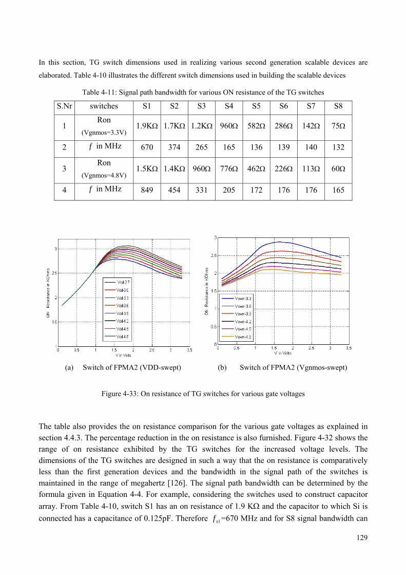
129
In this section, TG switch dimensions used in realizing various second generation scalable devices are
elaborated. Table 4-10 illustrates the different switch dimensions used in building the scalable devices
Table 4-11: Signal path bandwidth for various ON resistance of the TG switches
S.Nr switches S1 S2 S3 S4 S5 S6 S7 S8
1 Ron
(Vgnmos=3.3V) 1.9KΩ 1.7KΩ 1.2KΩ 960Ω 582Ω 286Ω 142Ω 75Ω
2 f in MHz 670 374 265 165 136 139 140 132
3 Ron
(Vgnmos=4.8V) 1.5KΩ 1.4KΩ 960Ω 776Ω 462Ω 226Ω 113Ω 60Ω
4 f in MHz 849 454 331 205 172 176 176 165
(a) Switch of FPMA2 (VDD-swept) (b) Switch of FPMA2 (Vgnmos-swept)
Figure 4-33: On resistance of TG switches for various gate voltages
The table also provides the on resistance comparison for the various gate voltages as explained in section 4.4.3. The percentage reduction in the on resistance is also furnished. Figure 4-32 shows the range of on resistance exhibited by the TG switches for the increased voltage levels. The dimensions of the TG switches are designed in such a way that the on resistance is comparatively less than the first generation devices and the bandwidth in the signal path of the switches is maintained in the range of megahertz [126]. The signal path bandwidth can be determined by the formula given in Equation 4-4. For example, considering the switches used to construct capacitor array. From Table 4-10, switch S1 has an on resistance of 1.9 KΩ and the capacitor to which Si is connected has a capacitance of 0.125pF. Therefore 1sf =670 MHz and for S8 signal bandwidth can

4 Architecture of Generic Intelligent and Adaptive Sensor System
130
be calculated to be 8sf =132 MHz. The signal path bandwidth for switches S1 until S9 is given in
Table 4-11 for different on resistance. In case of switches being used other than the capacitor array, the value of C to calculate the signal path bandwidth may be taken from the parasitic capacitances.
RCf
Π=
21 Equation 4-4
4.7.3 Amplifiers in FPMA2
The second generation of scalable devices was used to realize functional blocks like Op Amps, filters, fully differential amplifiers, instrumentation amplifiers etc. Amplifier topology similar to our previous investigation was deployed to design and test. Amplifiers with varying complexity are considered for investigation. These amplifiers are then used to construct more advanced circuits in hierarchical fashion.
4.7.3.1 Miller OPA Miller OPA is an established two stage structure with compensation scheme is considered for our investigation. The schematic representation of the Miller operational amplifier with second
Figure 4-34: CMOS Miller operational amplifier with second generation of scalable devices

131
Table 4-12: Comparison of Miller OPA specs constructed with unit and scalable devices
generation of scalable devices is shown in Figure 4-33. Unlike the circuit structure shown in Figure 4-16, the biasing scheme are modified with a simple way using resistor R1. The circuit structure along with the compensation capacitor incorporates a nulling resistor R2. The amplifier topology requires a total of 11 scalable devices (5*ST_NMOS2, 3*ST_PMOS2, 2*Scal_Res2 and 1*Scal_Cap2). The total bits therefore can be calculated from the Table 4-7 and is equal to 119 bits. The layout implementation of the complete mixed signal Miller OPA cell is shown in Figure B-1. The area consumption of the cell is given in Table 4-15. The differential pair transistors are implemented with the matched scalable transistor pair as shown in Figure 4-28(b). Apart from the differential pair transistors M1 and M2, M7-M8 and M3-M4 are also implemented with source coupled arrangement to save silicon area. In the mentioned transistor pairs, first two constitute NMOS pairs and the later is PMOS transistor pair. The sequence of digital data starts from M8, M7, M1, M2, M3, M4, M5, M6, R1 and finally ends with Cc. The compensation capacitor on the other hand, can be completely disconnected from the structure by turning off the switches connecting its top and bottom plates to function as a comparator. Extrinsic performance specs for Miller OPA comparing with unit and scalable devices are furnished in Table 4-12.
4.7.3.2 FC_OPA Folded cascode operational amplifier is a topology with better performance compared to the simple two stage amplifier as explained in section 4.4.6.3. The schematic representation of the folded cascode operational amplifier with the second generation of scalable devices is illustrated in Figure 4-34. The circuit structure has different biasing structure compared to the one discussed in section 4.4.6.3. The circuit consist a total of 24 scalable devices (9*ST_PMOS2, 13*ST_NMOS2, 1*Scal_Res2 and 1*Scal_Cap2). The structure therefore requires a total number of 262 bits.
S.Nr OPA
Parameters Miller OPA with unit devices
Miller OPA with scalable devices-FPMA2
1 Gain 80dB 81dB
2 Phase Margin 63.8°(Cc=4pF) 64°(Cc=5pF)
3 Gain Band Width 11.2MHz 10.8MHz
4 Offset 1.4nV 34nV
5 Input CMR 2.6V 2.8V
6 Output Swing 2.4V 3V
7 Slew Rate 36.1V/µSec 21.6V/µSec
8 Settling time 108nSec 550nSec
9 CMRR 83dB 95.9dB
10 Power Dissipation 4.5mW 4.41mW

4 Architecture of Generic Intelligent and Adaptive Sensor System
132
Figure 4-35: Folded cascode operational amplifier with second generation of scalable devices
The sequence of the digital data starts from M21, M20, M19, M13, M12, M14, M1, M2, M6, M7, M10, M11, M21, M3, M4, M5, M8, M9, M15, M18, M16, M17, Cc and R1. Along with input differential pairs, some other transistors having common source potentials are implemented in source coupled arrangement to save silicon area. The implemented transistor pairs are represented in Table 4-13. Extrinsic performance specs for FC OPA comparing with unit and scalable devices are furnished in Table 4-14. The layout of FC OPA is given in Figure B-1 and its area consumption is given in Table 4-15.
Table 4-13: Various differential pair transistors in FC OPA layout implementation
Number of NMOS transistor pairs
Implemented NMOS transistor pairs
Number of PMOS transistor pairs
Implemented PMOS transistor pairs
M19 & M20 M4 & M5
M12 & M13 M3 & M21 3
M1 & M2
3
M16 & M17

133
Table 4-14: Comparison of FC OPA specs with unit and scalable devices
4.7.4 Hierarchical Design
Hierarchical design splits/partitions the design space in several levels, starting from the lowest transistor level, building block level, and functional block level and finally to more complex system level. This can be easily understood from the example taken from the so far covered circuit and circuit implementations. In our case, unit devices like resistors, capacitors and transistors contributing to the scalable version forms the lowest level in the hierarchy. The scalable devices (ST_NMOS, ST_PMOS, Scal_Cap, and Scal_Res) built from these unit devices becomes the building block level. The third in the hierarchy is the functional block level; in our case operational amplifier (Miller OPA, FC_OPA, and GOPA) built with the scalable devices. The top most or the next level in the hierarchy is creating circuits using functional amplifier blocks along with building block levels to realize circuits like Instrumentation amplifier, Filters, Fully differential amplifiers, ADC’s etc. Some common and useful circuits employed in sensor signal conditioning are investigated in the upcoming sections for the hierarchical design.
4.7.4.1 Low Pass Active Filter Operational amplifiers realized with linear and non linear devices in the feedback to implement different circuits as discussed in chapter 3. A low pass filter is an important sensor signal conditioning block to filter out the noise. A simple low pass, single pole filter was explained in section 3.3.1 (a). A simple two pole, low pass filter circuit is shown in Figure 4-36(a).Figure 4-36(b) shows few of many possible values for Q using scalable devices. In this circuit arrangement folded cascode operational amplifier is used in a unity gain arrangement. From section 4.7.3.2, we
S.Nr OPA
Parameters FC OPA with unit devices
FC OPA with scalable devices-FPMA2
1 Gain 117.8dB 117.7dB
2 Phase Margin 62.8° 61.3°
3 Gain Band Width 4 MHz 3 MHz
4 Slew Rate 53.9 V/µSec 54.68 V/µSec
5 Settling Time 43 nSec 47nSec
6 CMRR 92.5 dB 92.25 dB
7 ICMR 2.7 V 2.7 V
8 Output Voltage Swing 3 V 3.003 V
9 Power Dissipation 0.34 µW 0.828 µW
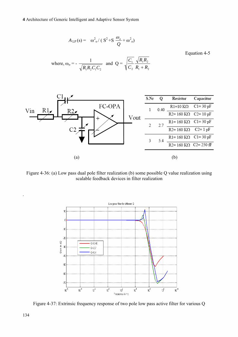
4 Architecture of Generic Intelligent and Adaptive Sensor System
134
A LP (s) = ω2o / ( S2 +S
Qoω
+ ω2o)
where, ωo = - 2121
1CCRR
and Q = 21
21
2
1
RRRR
CC
+
Equation 4-5
(a) (b)
Figure 4-36: (a) Low pass dual pole filter realization (b) some possible Q value realization using scalable feedback devices in filter realization
.
Figure 4-37: Extrinsic frequency response of two pole low pass active filter for various Q

135
know that FC OPA requires a total of 24 scalable devices. Therefore to realize a low pass two pole filter, a total of 28 scalable devices (3*Scal_Res2, 3*Scal_Cap2, 9*ST_PMOS2, 13*ST_NMOS2) are required. The total bits required to configure the structure can be calculated from the Table 4-8. The structure requires a total of 302 bits. The cut-off frequency of the filter is denoted by the Equation 4-5. The frequency response of the filter circuit for various values of Q is shown in Figure 4-37.
4.7.4.2 Fully Differential Operational Amplifiers In many sensing applications, amplifying the difference of the two input signals is a desirable feature as in the case of Zooming ADCTM [90]. Traditionally, this is carried out with a circuit structure called instrumentation amplifier as explained in section 4.4.7. Figure 4-38(a) [106] shows the recent way of realising a fully differential amplifier (differential input – differential output). The circuit structure was suggested by Dave Van Ess from Cypress semiconductors.
)21()16(11 VinVinaRaR
RaVinVout −+−
+=
)12()16(22 VinVinaRaR
RaVinVout −+−
+=
Therefore, )21(1621 VinVina
VoutVoutVdiff −=−=
Equation 4-6
(a) (b)
Figure 4-38: Fully differential amplifier with FC OPA and internal gain settings resistors realised through second generation of scalable devices (a) recent topology (b) traditional design

4 Architecture of Generic Intelligent and Adaptive Sensor System
136
The circuit is built with two programmable folded cascode operational amplifiers and three scalable resistors as shown in Figure 4-38(a). The three resistors are used to define the gain of the circuit. The output equation of the fully differential amplifier is given in Equation 4-6 [106]. For the sake of simple calculation, R4 is splitted into two resistors of ratio a1 and a2. But in real implementation, it is realized by a single resistor. The fully differential structure has the gain defined by the resistor combination. A simple differential low pass filter could be realized by adding RC components to the differential inputs. Here it should be noted that, in traditional approaches, a common mode feedback circuitry is essential to establish a stable output and the gain of the circuit is defined through feedback resistors as shown in Figure 4-38(b). Even though the traditional approaches consume less area than the recent ones, choice was based on the fact that no common mode feedback circuits (CMFB) circuits are necessary. Secondly, the fully differential structures can be extended to instrumentation amplifier by adding a difference amplifier to it. The fully differential circuit structure needs a total of 557 bits (2*FC OPA + 3*scalable resistors=524+33). The digital bits are fed in such a way that the scalable devices, inside the amplifier are configured first. The sequence of the digital data path is FC_OPA1, FC-OPA2, R3, R4 and R5. Figure 4-38 shows the transient behavior of the circuit.
Figure 4-39: Simulated transient response of dynamically reconfigurable fully differential amplifier with
internal gain settings
4.7.4.3 Instrumentation Amplifiers The importance of the instrumentation amplifier circuit structure is well understood from chapter 2 and section 4.4.7. In this section, instrumentation amplifier topology is constructed with some

137
modification to the traditional circuit shown in Figure 4-20. The novel modified circuit of the In Amp with dynamic calibration capabilities of its building blocks is shown in Figure 4-39. The In Amp is built with 3 programmable FC OPA and 7 scalable resistors (7*Scal_Res2). The folded cascode building blocks are in turn constructed using the second generation of scalable devices as shown in Figure 4-33. Apart from the amplifiers and resistors, the circuit has additional switches called the Calibration switches.
Calibration switches (Cs) are the next level of switches used in the hierarchy. Cs is nothing but the transmission gate switches as represented in Figure 4-8. The dimensions and the on-resistance of these switches are provided in Table 4-10. Care should be taken in designing the calibration switches on-resistance, because the on resistance of these switches can add to the internal feedback resistance of the In Amp to determine the loop gain of the circuit.
)21)(2121(
45 VinVin
RR
RRVout −+= Equation 4-7
The methods suggested in section 4.4.3 to reduce the on resistance of the switches are useful here. The output characteristics of In Amp for various on resistance of the switches are shown in chapter 5 (section 5.4.3). The output of In Amp is given by the Equation 4-7. Where R1 = R3, R5 = R7 and R4 = R6. Calibration switches assist in hierarchical calibration of the instrumentation amplifier. This means that when all 7 Cs switches are turned on, a complete instrumentation amplifier is constructed. When all Cs are turned off, then 3 individual amplifiers are available for testing or calibration. A common control signal for all 7 Cs switches is provided by an additional I/O pad. Using appropriate voltage levels either “1” or “0”, circuit can be configured for calibration or complete operation respectively. Therefore a total of 3 calibration cycles are required for the individual amplifiers and in total of 4 cycles are essential for calibrating the whole instrumentation amplifier. Principally, all the scalable resistors can also be calibrated together. But due to the limitation of the number of Input /Output pads for the selected chip package, and to get benefited from the usage of the same measurement and test prototype, this option was ruled out. Nevertheless the resistors can be calibrated together with the amplifiers by reading out and comparing the digital data output with the digital data input used to configure the analog arrays building the In Amp. The total number of bits required for configuring In Amp can be calculated from the Table 4-8 to be equal to 863 bits (3*FC OPA= 786 bits) + (7*Scal_Res2=77).The layout implementation of In Amp is shown in Figure B-1. The area consumption is given in Table 4-15. Matching properties are inherited from FC OPA building block by the use of various matched transistor pairs as explained in sections 4.7.1 and 4.7.3.2 the total number of matched transistor pairs used in In Amp are 18. The sequence of digital data path starts from OPA1, OPA2, OPA3, R1, R2, R3, R4, R5, R6 and R7.

4 Architecture of Generic Intelligent and Adaptive Sensor System
138
Figure 4-40: Instrumentation amplifier with hierarchical calibration capabilities
4.7.4.4 On-the-Fly Hierarchical Calibration – Offline and Online
Dynamic hierarchical calibration of instrumentation amplifier was discussed in the previous section. The so performed calibration is defined as offline, where the calibration of 1 OPA results in interrupting the functioning of the In Amp. Functionality of the In Amp is restored back into operation after all the building blocks are calibrated. This is of course a time consuming process.
In order to save time and keep In Amp functional while calibration of single OPA is performed, second type of calibration called online is preferred. In this approach, a fourth OPA is used in Amp circuit. Under normal operation of In Amp, this extra OPA is non-functional. But at the time of calibration, this extra OPA comes into use. Revisiting the calibration procedure explained in section 4.7.4.3, While OPA1 is being calibrated, the extra OPA introduced will come into action for OPA1 thereby the working of Instrumentation amplifier will not affected while calibrating one of the three OPA. This procedure is repeated for the other Op Amp’s as well (OPA2 and OPA3). This alternative online approach is efficient enough with respect to time, but on the contrary occupies more area compared to the other approach. The software part of this work is explained in [74].
4.7.4.5 “Soft Sleep” mode – Low Power Design Issues
In most of the battery driven, mobile and implantable products power consumption is of utmost importance. One predominant approach in digital domain is the use of sleep mode, where the

139
required circuit or module comes in action after a small initiating signal is provided else not in a dormant mode called the sleep mode eventually saving power. The system then requires an awake signal to bring back the functionality. In our programmable analog array approaches, the sleep mode techniques can be deployed to the signal conditioning interface electronics; in particular during calibration idle amplifiers can be switched-off. Additionally, there is a novel option now defined the “soft sleep” mode [123]. In this reduced power mode approach, amplifiers are programmed to a very low power consuming configuration, making the system to operate slowly with very less power. But once an activating signal / awake signal is instantiated, the circuit comes back to be fully vigilant. The activating or wake signal is provided based on any certain sensor activity. Hence, two different power consuming configurations are required. These patterns can be stored in an EEPROM arrangement.
4.7.5 Noise Issues
Noise is considered to be the most unwanted excitation present in any circuits. Noise are difficult to model and hard to eliminate. It is necessary to consider the reduction of noise in low power or low voltage system as the signal levels are small.
4.7.5.1 Signal Integrity Challenges
Switching Noise: In modern mixed signal approaches, where both analog and digital combination is common. The transient spikes or noise induced due to switching activity of the digital circuits like the shift registers (in our case) can propagate to the analog circuits through the common substrate and eventually cause variations in its performance. Modelling and simulation of such induced noise propagating through the common substrate are tedious and difficult as they are not constant and mostly vary with time. On the other hand, the source of noise due to switching is indeed not determinable.
Cross talk: Another form of noise arising is due to electromagnetic interferences from the power lines. In a traditional manner, by appropriate placement of the global power and ground lines possibly reduces the effect. In the ST_NMOS2 & ST_PMOS2, finger like arrangement with alternatively placed VDD and GND signals are carried out. The source of interfering noise signal can arise from/due to clock feed through, thermal effects and also from external measurement and testing devices. Even though the noise are difficult to eliminate, the variations caused in the performance of the circuits by these noise can be compensated through reconfiguring the circuits when deployed with the optimizing software in the loop.

4 Architecture of Generic Intelligent and Adaptive Sensor System
140
4.7.5.2 Matched layout
Complex signal nature of the analog design demands human intervention (full custom) in creating layout for simulation verified circuits with the help of layout tools. Parameterised cells (P-Cells) are of good support in creating such full custom layout. Because of this reasons, analog design cycles are long and prone to errors. In certain layout implementations, use of P-Cells eventually consumes more die area. Hence here care should be taken while creating the layout manually as the placement of the same cells in different locations of the wafer exhibit different properties. Hence use of careful and protective layout techniques is highly appreciable. Matching is one traditional way of obtaining the desired component value unaffected by the manufacturing tolerances. These physical design considerations are very important because the effects due to these variations are not amenable even when through the optimization in the loop arrangement is deployed (from software point of view). Table 4-15 shows some of the hardware realisation within the scope of this thesis with matching techniques. Unlike the non programmable analog circuits, it is more challenging in heterogeneous type of programmable analog array type of circuits to provide complete matching because of the wide range of components, placement issues, and routing between the digital selection circuits.
4.8 Flexibility, Area and Fault Tolerance
4.8.1 Modes of Flexibility
Flexibility and area are the two parameters that have to be traded off against each other. Area increases with increase in flexibility. Fault tolerance of the programmable structure depends directly on the available flexible range of the system. In this section various levels of flexibility conceived through different hardware realizations by the investigated methodology are summarized in this section. Figure 4-41 show pictorial representation of the various flexibility schemes.
4.8.2 Fault Tolerance and Area
Table 4-15 gives the comparison of the area used versus area available for the cells realized with varying complexity with two different generations of scalable devices. The table also provides the matching information of the implemented layout. Cost and flexibility are the two contradicting factors which have to be considered in programmable analog approaches to have better fault tolerant capability. Table 4-15 gives a comparison of exhibited fault tolerance for the various implemented cells.

141
Figure 4-41: Various modes of flexibility conceived
Table 4-15: Comparison of used to available Area
S.Nr H/W Implemented Cells Available Area in
mm2
Used Area
In mm2
% of used to
Available Area
Layout
Matching
Fault
Tolerance
Miller OPA 0.249 0.0085 3.4
Folded Cascode OPA 0.421 0.018 4.2 1 FPMA
Instrumentation_Amp 1.998 0.0663 3.3
No Better
GOPA 0.828 0.0085(Miller)
0.018 (FC)
1.0
2.1 Best
2 FPMA1B SubThreshold Miller
OPA 0.219 0.0082 3.7
No
Better
Miller OPA 0.208 0.0083 3.9
Folded Cascode OPA 0.319 0.017 5.3 3 FPMA2
Instrumentation_Amp 1.247 0.066 5.2
Yes Better
Fully Differential OPA 0.723 0.040 5.5 Yes Better 4
Case
Studies Selective Node Flexibility
Three case studies for offset, Power consumption and speed Partial Reduced
4 Architecture of Generic Intelligent and Adaptive Sensor System
142
4.9 Evolvable System-on-Chip Sensor System / Generic off the Shelf Chip
Due to rising cost of manufacturing of wafers, risk minimization is very essential. System on Chip is developed to address these problems to integrate electronics of diverse nature in one single chip. Moreover, MEMS/NEMS are becoming more and more part of our daily life in the form of sensors. New sensor technologies are coming to the market every day, signal conditioning becomes challenging. Compatibility of the planar IC process with some sensor technology (MEMS/NEMS) has provided integration capabilities between the sensor element and the signal conditioning electronics. The more important is the issues of integration between them to exhibit “System on Chip” embeddable sensor system. Besides having some advantages like high performance, since all circuits are in one chip, less area, etc, other key issues concerning SoC are listed below,
1) Operation voltages of the sensor element manufactured through various planar technologies like CMOS, MEMS and the signal conditioning devices can be same when implemented in the same substrate as in the case of image sensors or it need not be the same, when implemented on different substrate with different technology (MEMS, High Voltage technologies, etc). Power dissipation issues originating because of the varied voltage levels are different.
The generic sensor signal conditioning interface IC discussed in the earlier sections could be used in as a single off the shelf chip on a PCB level or could be integrated in conjunction with MEMS. In case of MEMS integration, level of granularity and flexibility used in realising interface circuits are important, if not the total area together with MEMS will be enormous. In such case, flexibility applicable to only selective nodes would be preferable. Example of such selective node flexibility approach was elaborated in section 4.4.6.2. MEMS based sensors are applied to vast range of fields like industry automation and automobile industries. The point here to note is that, MEMS technology sensor are not always fortunate enough to work with the same voltage level of the chosen technology in this thesis work (Austriamicrosystems- 0.35 µm CMOS process with 3.3V to 5V supply voltage). Therefore, in order to get sufficient information of the used resources in various sensing application with different voltage levels are collected, studied and listed in Table 3-2. The device and component dimensions are not only important for address the supply voltage problems but also to define the level of flexibility/ granularity to be pursued for high voltage application
2) Simulation/validation issues or tools to combining the vast sensor modules with the interface to perform a kind of global simulations. Debugging will also be complex.
3) Recognition of various sensor types on integration with conditioner. Current methods are based on Plug n Play, and Advanced Plug and Measure (APM) [87] and DSiTTM [88] when the sensor elements are not implemented in the same substrate as the conditioning device.
In the scope of this thesis work, integration of sensor element is not carried upon but instead foreseen to create a generic sensor system as shown in Figure 4.42. The test chip can be used in as

143
single instance or together with the sensors. The dotted line indicated that the ADC be optional (on chip/off the chip). The generic system with the adaptive sensor signal conditioning circuit including dedicated evolutionary software is expected to evolve. Embedding the whole set up is challenging.
Figure 4-42: Generic Sensor System

5 Experimental Set Up and Results
144
5. Experimental Set Up and Results
5.1 Dynamic Reconfigurable Stand Alone Board
This section describes the measurement set up of our dynamic reconfigurable hardware. The first prototype depicted in Figure 5-1 is the simple 515-C embedded system of PHYTEC, which serves for programming the chip to obtain measurement results and for advanced analog chip designer training (chapter 6). The prototype is connected through RS 232 interface from the host computer which generates the bit patterns with the help of software called Keil µVision and are downloaded to its internal memory through PHYTEC Flash Tools version 98. The system serves to selectively configure the three cells of the chips (FPMA1/FPMA2) by clocking in configuration patterns that were generated based on manual design activity or extrinsic simulation runs. The performance measurement was carried out by appropriate feeding in of the bit patterns so as to configure the analog structure in it [132]. The bit patterns are bred in several ways. One way is to generate bit patterns manually or using C - code developed at ISE according to the device dimensions used during the design phase with the tools like Cadence, Pspice and Matlab. The so generated device dimensions are then converted into binaries according to the Table 4-1 and Table 4-8. The converted binary bit chain differs according to number of scalable devices used in realizing the established analog structures. The total bits required for the various hardware implementations are provided in Table 5-1. These binary bits are downloaded to the shift register for configuring the switches connecting the unit devices. Output is thereafter measured after a protective enable signal, which isolates the operation of digital domain from the analog domain. Since the configuration bits are to be downloaded to the shift register, a fixed sequence of feeding in the bit patterns is followed according to the wiring of the scalable devices in realizing different amplifier topologies. In our work, we define a digital interface for the requirement of programming, or for calibrations purposes. In addition to the normal pins of the OPA, a serial_In (D) pin to feed the shift register, 2 pins for non overlapping clock (CLK1, CLK2), and an Enable (EN) pin are required. In total FPMA1 and FPMA2 have 40 pins manufactured in dual inline package (DIL). The enabling signals make sure that the switches do not interact with the circuit operation when turned off until a valid switch pattern bits are fed into the circuit. The protective logic used for safe isolation and operation was discussed in section 4.4.4. Various PCB test plug boards with different feedback arrangements of the amplifier can be plugged onto the main board with the chip for the common measurement and application topologies as shown in Figure 5-1(a) (b) and(c). By the experiments, only two of the three cells in the first generation chip (FPMA1) were found operational. The most complex instrumentation amplifier cell suffered from a trivial design error and required a redesign to be functional, which is addressed and fixed in the second generation chip namely FPMA2 with advanced calibration capabilities and is found functional. A second prototype for intrinsic evolution, related to self-reconfiguration or –trimming, has been established in parallel work [74]. Measurement employs a PC-based Lab view slot card, i.e., still non-embedded hardware. In this

145
(a) Complete measurement set up
(b) PHYTEC mini MODUL C-515 with 3 test plugs (c) Other test plugs used for measurement
Figure 5-1: Dynamic reconfigurable stand alone test set up

5 Experimental Set Up and Results
146
case, bit configuration was generated based on fitness function using evolutionary approaches like PSO / GA.
5.2 Mixed Signal Test Sequence
Mixed-signal test sequences discussed in section 5.1 can be formulated into the following steps,
1. First, selection of one of the cells to be tested (depending on the version of the designed test chip).
2. Secondly, appropriate digital data according to the design are fed into the shift registers to store the configuration patterns with the assistance of two phase gated clocking scheme.
3. Next, a protective enable signal (isolation signal) is activated to transfer the configuration patterns stored in the shift registers to the scalable analog blocks.
4. After successful selection of the unit devices from the array, analog inputs are provided with a time allowance to settle down after configuration. Settling time allowance has nothing to do with the amplifier settling time, but instead is the time for safe and sure configuration.
5. Analog output is thereafter measured according to the type of measurement circuits or test plugs used.
Figure 5-2: Timing diagram or test sequence of mixed–signal mode design

147
More clear picture of the above described test sequence of the mixed signal design is shown in Figure 5-2. In this case, the amplifier is configured in an inverting arrangement with the feedback resistors in the ratio of 5. Table 5-1 gives the full details of the available cells in both version of the manufactured test chips, number of scalable devices required and the total bits requirement of the individual cells. Figure 5-3 shows the snap shot of the generated bit for configuring an instrumentation amplifier in FPMA2. The converted bits are based on manual design in CadenceTM design environment. Results obtained for the various implemented cells in extrinsic and in intrinsic fashion are furnished in from sections 5.2 to section 5.5.
Table 5-1: Reconfigurable bit requirements for the various cells implemented in the test chips
S.Nr H/W Implemented Cells No. of Prog. Devices Total bits
Miller OPA 13 (5*S.pmos, 6*S.nmos, 1*S.res, 1*S. cap) 138
FC OPA 25 (10*S.pmos, 13*S.nmos, 1*S.res, 1*S. cap) 270 1 FPMA
In_Amp 131 (3*FC_OPA, 56*SR) 1258
Miller OPA 11(3*S.pmos, 5*S.nmos, 2*S.res, 1*S.cap) 119
FC OPA 24 (9*S.pmos, 13*S.nmos, 1*S.res, 1*S.cap) 262 2 FPMA 2
In_Amp 79 (3*FC_OPA, 7*S.res) 863
Figure 5-3: Feeding in bit patterns for Instrumentation Amplifier in FPMA2 for 18 dB gain

5 Experimental Set Up and Results
148
5.3 Measured Results of FPMA
5.3.1 Results of Miller Op Amp
(a) Unity Gain (b) Inverting amplifier arrangement R2/R1=6
(c) Non-inverting amplifier arrangement R2/R1=2 (d) Open loop
(e) Miller OPA as Differentiator (f) Miller OPA as Integrator
Figure 5-4: Measurement results of Miller OPA in FPMA1

149
Figure 5-5: Miller OPA as comparator with Cc turned off

5 Experimental Set Up and Results
150
5.3.2 Results of Folded Cascode Op Amp
(a) FC OPA as Differentiator (b) FC OPA as Integrator
(c) Non-inverting amplifier arrangement R2/R1=2 (d) Inverting amplifier arrangement R2/R1=6
(e) Open loop (f) Unity Gain
Figure 5-6: Measurement results of folded cascode OPA in FPMA1

151
5.4 Measured Results of FPMA2
5.4.1 Results of Miller Op Amp
(a) Miller OPA-Unity Gain (b) Miller OPA in Non Inv. arrangement
(c) Miller OPA as Differentiator (d) Miller OPA in open loop gain
(e) Miller OPA-ICMR (f) Miller OPA –Output voltage swing
Figure 5-7: Results of Miller OPA in FPMA2
ICMR Output VoltageSwing

5 Experimental Set Up and Results
152
(a) Miller OPA-Gain (b) Miller OPA - Phase
(c) Miller OPA - CMRR (d) Miller OPA- PSRR+
Figure 5-8: Results of Miller OPA in FPMA2_Continued
PSRR+ CMRR
Gain Phase

153
5.4.2 Results of Folded Cascode Op Amp
(a) FC OPA in Unity Gain (b) FC OPA in open loop
(c) FC OPA in Non Inv. arrangement (d) FC OPA in Inv. arrangement
(e) ICMR of FC OPA (f) Output voltage swing of FC OPA
Figure 5-9: Results of Folded Cascode OPA in FPMA2

5 Experimental Set Up and Results
154
(a) FC OPA-Gain (b) FC OPA -phase
(c) FC OPA-CMRR
Figure 5-10: Results of folded cascode OPA in FPMA2_continued

155
5.4.3 Results of Instrumentation Amplifier
(a) Non inv In Amp at 1.55 MHz (b) In-Amp in Inv. arrangement
(c) Measured gain compared with product for –3dB (d) In_Amp for various measured gains
(e) Slew rate & Settling time (f) In Amp for various switching voltage
Figure 5-11: Results of instrumentation amplifier in FPMA2

5 Experimental Set Up and Results
156
5.4.3.1 Hierarchical Calibration Results of instrumentation Amplifier
(a) FC OPA1 of In Amp in non-inv arrangement (b) FC OPA1 of In Amp in Inv. arrangement
Figure 5-12: Measurement results of 1of 3 FC OPA’s in instrumentation amplifier during calibration in
FPMA2
Figure 5-13: Measurement results of Instrumentation Amplifier in FPMA2 is compared with the commercial products

157
5.5 Reliability Analysis and Drift Compensation
5.5.1 Yield Considerations for Reconfigurable Circuits In modern era, the pace with which the products turn up to market is becoming rapid and rapid. Hence to ensure reliability and quality of the manufactured product, high Yield is very crucial [3] in general, reconfigurable analog chips offer new opportunities of increase, but also require adapted analysis approach. for instance occuring deviations and potential reconfiguration capability by expended switching resources has to be analyzed. The two generation of dedicated test chips were manufactured through Multiple Project Wafer (MPW) runs of IMEC through EUROPRACTICE and were subjected to test. 20 samples of each test chips were provided from the manufacturer. Out of 20 FPMA1 chips, 4 were used in the loop with optimization procedures and the rest were found functional. Whereas in the case of FPMA2, 1 chip is employed for optimization procedures, 18 chips were found functional and in 1 chip variations are noted. Apart from being used in testing, some of the chips were constantly deployed in the optimization loop since 2006. The chips were also used during several demonstrations for industrial and research visitors as well as for students. The issues of yield are very important in non programmable circuits because, the variations caused due to the manufacturing process and tolerances causes variations in the performances of the circuit which consequently changes the yield. Whereas, in programmable approaches, the variations noticed can be compensated through appropriate reconfiguring. Most recent approaches come from the field of evolutionary computing, where the compensating algorithm controls the hardware in the loop to compensate instant specific deviations. This method is referred to as intrinsic evolution approach, in which the optimizing software determines the reconfiguration patterns based on fitness functions.
Figure 5-14: General architecture of intrinsic evolution environment.

5 Experimental Set Up and Results
158
Figure 5-15: Block diagram of multi-objective evolvable system developed by Peter Tawdross together with
the dynamically reconfigurable hardware platform and assessment circuits.

159
In a separate work, a second prototype was used to evaluate the chip designed in the scope of this thesis work through optimization techniques by Tawdross et al. In his work, to show the compensation capabilities through intrinsic evolution, the test chip was initially heated with solder rod and then the variation thereby produced is compensated. The general architecture of the intrinsic evolution environment is shown in Figure 5-14. Figure C-1 shows the heating of the chip to invoke deviations. The measurement setup was later modified as shown in Figure 5-15. The architecture of the multi objective evolvable system shown in Figure 5-15 mainly consist of two blocks, namely processing unit and reconfigurable hardware along with the measurement circuits.
The optimizer in the processing unit runs the bio-inspired algorithms like GA, PSO, etc. Here approaches suitable for dynamic environment were studied and implemented. The device dimensions created by the optimizer based on the fitness functions and were then converted to bit patterns. The bit patterns converted vary according to the type of hardware. Table 4-1, Table 4-8 and Table 5-1 illustrates the bit pattern requirement for different hardware realized. Apart from programming the cells in the hardware (FPMA1/FPMA2), separate bit patterns were generated to select the assessment circuit to which the designed programmable amplifiers were connected to determine its parameters like offset, settling time, CMR, output swing, power consumption etc. Appropriate test signals required for testing the analog hardware are generated by the processing unit and are fed to the board through DAC as shown in the Figure 5-15. The post processing block in the processing unit obtains the information from the board through ADC and uses it for on-line controlling schemes. The data fed in to the shift registers of the mixed-signal amplifiers are cross checked by comparing to the out data from the shift registers by the post processing block. Post processing block also compares the obtained result with the desired results. In case, the obtained results are not the desired then, the optimizer is brought back into operation for better configuration during on-line monitoring for dynamic operating conditions. More information’s regarding optimization procedures are explained in detail by Peter Tawdross in his work [74].
In this thesis work, we are just the users of his optimization techniques and works for testing the robustness of the hardware and to illustrate the instance specific drift compensation capabilities of the hardware itself. The PCB board with the reconfigurable hardware shown in Figure 5-15 has many measurement circuits. Several passive and active feedback components can be added to the amplifier for measuring its specification as described in chapter 3. Some key amplifier specifications measured for 15 different samples of the two test chips designed, namely FPMA1 and FPMA2 are shown in Figure 5-16, Figure 5-17, Figure 5-18 and Figure 5-19.

5 Experimental Set Up and Results
160
(a) Offset (b) CMR
(c) Output Swing (d) Power Consumption
(e) Rising SR (f) Falling SR
Figure 5-16: Statistical comparison of 15 samples of FPMA1 and FPMA2 for Miller OPA.

161
(a) Rising Settling Time
Figure 5-17: Statistical comparison of results for 15 samples of FPMA1 and FPMA2 for Miller OPA
The cost and area of the evolution board increases depending on the number of assessment circuits built. This might not be fortunate for an embedded system. Another limitation observed in this automated approach is that, transient specifications like settling time of the amplifiers becomes difficult to measure because of the ADC conversion rate being slower than the OPA.
(a) Offset (b) CMR
Figure 5-18: Statistical comparison of results for 15 samples of FPMA1 and FPMA2 for folded cascode OPA.

5 Experimental Set Up and Results
162
(a) Output Swing (b) Power Consumption
(c) Rising SR (d) Falling SR
(e) Rising Settling Time (f) Falling Settling Time
Figure 5-19: Statistical comparison of results for 15 samples of FPMA1 and FPMA2 for folded cascode OPA.

163
5.5.2 Instance Specific Drifts and Drift Compensation
Ideally, in a carefully fabricated wafer containing circuits, we would expect all of the circuit on the wafer to be functional. In practice, number of good exemplar might vary from 100% to 0%. The cause of failure can be due to several factors like, manufacturing procedure, bad design, etc. In case of programmable devices with redundant circuitry, defective circuits are replaced by switching on to good circuits. Section 5.5.1 shows the consistency check for 15 samples based on certain measured amplifier specifications as shown in Figure 5-16, Figure 5-17, Figure 5-18 and Figure 5-19. Most of the measured specifications remain nearly the same except for certain other specification like offset. It can be clearly noted from Figure 5-16(a), that the offset variation is drastic and uneven. In order to compensate these variations, the corresponding test chips are subjected to optimization procedures individually. Figure 5-20, Figure 5-21 (a) and Figure 5-21(b) shows the minimized drifts in the specification through re-optimization for various hardware cells. Table 5-2 shows the betterment in performance obtained after performing reoptimization to compensate drifts.
Table 5-2: Drift compensation through dynamic reconfiguration
S. Nr Hardware
Implementation
Instance. Spec.
Deviations,
Σ/N (Offset)
Instance. Spec.
Compensation,
Σ/N (Offset)
Betterment
In %
Σ/N (Offset)
1 Miller OPA in FPMA1 1.67 mV 0.48 mV 71.26 %
2 Miller OPA in FPMA2 0.94 mV 0.37 mV 60.63 %
3 Folded cascode OPA in FPMA1 3.46 mV 0.346 mV 90 %
4 Folded cascode OPA in FPMA2 3.77 mV 0.125 mV 96.68 %

5 Experimental Set Up and Results
164
(a) Miller OPA in FPMA1
(b) Miller OPA in FPMA2
Figure 5-20: Statistical comparison showing instance specific deviation in offset and its compensation configurations for 15 test samples of Miller OPA in FPMA1 (a) and in FPMA2 (b)

165
(a) Folded cascode OPA in FPMA1
(b) Folded cascode OPA in FPMA2
Figure 5-21: Statistical comparison showing instance specific deviation in offset and its compensating configurations for 15 test samples of folded cascode OPA in FPMA1 (a) and in FPMA2 (b)

6 True Front to Back Analog IC Designers’ Training
166
6. True Front to Back Analog IC Designers’ Training
6.1 First Generation FPMA involved in Teaching
Integrated dedicated electronics are essential to the modern information world as a key issue to information technology. The course work for the students specializing in microelectronics/integrated systems at the department of electrical and computer engineering in TU Kaiserslautern are structured in such a way that, after a basic introduction to the field of electronics, measurement and instrumentation, focus on semiconductor physics and fabrication, design of microelectronic circuit and systems, and design methodology of digital, analog and mixed-signal integrated circuits and systems are provided. In the basic courses, in addition to theoretical knowledge and exercises, demonstrations and self study opportunities are provided, based on Matlab and PSPICE. The objective of the sensor electronics teaching at the chair is to introduce the students to the subject of analog and mixed-signal integrated circuit design. The course starts from the basic models of semiconductor devices, covers fabrication and basic and matched layout techniques and advances to the design and implementation of more complex circuit structures like comparators, operational amplifiers, filters, image sensors, etc. The course outlines the state of the art of reconfigurable analog electronics as well.
Analog and mixed-signal sensor electronics comprise a small yet essential fraction of a large variety of embedded and integrated systems in industrial application systems. The number of devices used in realizing such analog and mixed-signal circuit structures is much less compared to its massive parallel counterpart, namely digital. However the design of each device requires excessively more care and experience. The task of designing an analog integrated circuit requires theoretical as well as tool skills. It is a particularity of the reported teaching activity, that state-of-the-art tools and technology are employed and combined or merged with the theoretical part.
It can be observed that the challenges of the tedious learning process of the required skills are not picked up by the sufficient number of the students to meet industry demands. In particular to the booming sensor and MEMS industries, and to attract more students to this topic, the chair 2 offers several design courses that combine theoretical and practical skills based on state of the art tools and technologies. Students elaborate individually or in small groups analog / mixed signal design projects. Commonly, students go through the complete design flow until tape out. However, due to common timing constraints in students curricular, they miss the chance to do measurement and testing to their design after turn-around time. In our approach, drawing from research work and results on dynamically reconfigurable sensor electronics, we amend this problem by giving the students the opportunity to download their dimensioning solution into certain reconfigurable devices and to carry out testing and measurement activities to characterize their design instantiated by reconfigurable device. For this aim, we introduce the True Front to Back (TFB) Analog IC Designers Training Kit, used in the CAD laboratory at the Institute of Integrated Sensor system 2 Institute of Integrated Sensor Systems, TU Kaiserslautern

167
(ISE) in TU Kaiserslautern for various engineering curricula. This chapter will give the details of the teaching concepts and state of implementation, and typical results for common student design and measurement activities. Finally, we will give an outlook on up-coming advanced reconfigurable chips extending our teaching concepts.
Figure 6-1: Design flow for analog integrated circuits
Some similar teaching projects at the IC level are offered at the following research institutes.
1) C. M. Twigg et al of Georgia Institute of Technology gives a training platform for characterization of pFET within CAM of his first generation FPAA. In the second generation FPAA comparators were synthesized. More details of the FPAA design by this research group could be found in section 2.3.10 [82].

6 True Front to Back Analog IC Designers’ Training
168
2) J. Kampe et al of TU Ilmenau provide a Rapid Development Kit (RDK). RDK is based on the EPAA structure explained in section 2.3.9. Here, similar to the TFB explained in this thesis work, users of RDK can benefit from transistor level design, placement and routing and validation procedures [122].
3) Through oral conversation with the research partner university, available of IC teaching at coarse granular level to design low pass filter was familiarized. More information of this research group activity was given in section 2.3.2.
Students are introduced to concepts of hierarchical design, mixed-signal and mixed-mode design, and exercise the studied concepts based on Cadence DFW II and Austriamicrosystems Hit-Kit and 0.35µm CMOS technology. The major steps in the analog integrated circuits design process are shown in Figure 6-1. It is observed that during most of the conducted courses, students were able to precede up-to the level of post layout simulations in their various design tasks given to them as individual or group semester projects. In some design cases participants could proceed to the level of tape out. Several Multi-Project-Chips (MPC) and research chips with course cells have been manufactured in the past. The opportunity to obtain a sample of one’s own chip was found to be very motivating for the students. But due to the tight timing of the curriculum of the students and due to the turnaround time of the design from the fabrication site (around 8-12 weeks), most students missed the chance of performing the important testing and measurement step in the design flow. So, the experience of the students was limited to CAD and simulations. Physical characterization and mandatory revisions of the design due to the findings were left for further professional exposure.
Figure 6-2: True front to back analog IC designers training kit

169
In this chapter, TFB analog IC training kit is presented, which enables the students with minor restrictions to completely go through the design flow in analog/mixed signal chip design of certain cells. In our approach, drawing from our research work and results on dynamically reconfigurable sensor electronics, we amend this problem by giving the students the opportunity to download their dimensioning solution into certain reconfigurable devices and to carry out testing and measurement activities to characterize their design instantiated by reconfigurable device. Table 6-1 gives a typical specification requested for a custom designed Miller amplifier, which is one of the basic and simple tasks given as student’s projects. Other amplifier cells, e.g., folded cascode, or instrumentation amplifier can serve here too. The common determination of a unit length, i.e., 1µm, becomes mandatory here, as the reconfigurable device has just this restriction. Following common ad hoc procedures or design plans [7], students have to dimension the circuit by manual calculations. Table 6-1 gives the dimensioning result for the requested specification from; say for example, designer 1. These device dimensions will be converted to configuring bits, and then downloaded, and subjected to measurement and assessment.
Training Kit: An immediate benefit of the designed chips and prototype is its use in education. Designers can immediately generate and download their design configuration and can do measurements without being subject to the delay imposed by the turnaround time. In order to configure the analog chip, designers at the ISE are advanced by the flow depicted in Figure 6-4, which was developed in ISE and remains the basic component of the sensor electronics design and application lecture and lab. The CAD laboratory course participants at the ISE were taught to design hardware for sensor signal processing, neural signal processing as well as the integration of sensors and electronics in CMOS technology e.g., image sensors. For this aim a cluster of Linux PCs / SUN workstations are available for design. Cadence DFW II tool obtained from EUROPRACTICE is available and currently, the Design -Kit for the 0.35µm CMOS technology of Austriamicrosystems is installed and used for teaching and research. During CAD laboratory teaching, participants were taught to understand and design analog and mixed signal circuits and chip design techniques. At the end of the course, they were subjected to design established analog circuit topologies. After successfully performing the related simulations at the computer based simulator level, they can proceed to validate their design at the physical level by appropriate programming of the available dynamically reconfigurable test chip namely FPMA1/FPMA2. At our institute, a software environment in C programming language was developed to convert the net-list of the designed circuit structures into the essential bit patterns [81]. Figure 6-3 shows the snap shot of the converted bit patterns for Miller topology. These bit patterns are then fed to the prototype for performance validation as explained in chapter 5. The training kit provides the designers to work in the loop until the desired performances are achieved. Through this the students/designers get a chance to get them familiarized with the full design sequence starting from design up to testing and measurement. Figure 6-2 shows the simple 515-C embedded system of PHYTEC, which serves for programming the chip to obtain measurement results as well as for advanced analog chip designer training. Table 6-1 shows the transistor dimensions used for the topology in Figure 4-16 and its equivalent bit patterns. Some key specifications of the operational amplifier obtained by a designer are also furnished in this table.

6 True Front to Back Analog IC Designers’ Training
170
Table 6-1: Miller OPA characteristics with aspect ratios and corresponding bit patterns
S.Nr Op Amp characteristics
Specification Request
Obtained Result _Designer 1
Device
Sequence
in FPMA
Device Dimensions
(L=1µm)
Corresponding
Bit Patterns
1 Open loop gain >70 dB 72 dB C1 4 pF 100100000
2 Gain band width 1 MHz 5 MHz M6 W = 154µ 10010111111
3 Phase margin >60° 60 ° M7 W = 2µ 00000010000
4 CMRR >80 dB 86.7 dB M2 W = 66µ 01000010000
5 Common mode range -0.8 V to +0.8 V - 1.4 V to + 1.4 V M1 W = 66µ 01000010000
6 Output range -0.35 V to +0.35 V - 1.3 V to + 1.3 V M5 W = 154µ 10010111111
7 Voltage supply -1.65 V to +1.65 V -1.65 V to +1.65 V M4 W = 1µ 00000001000
8 Slew rate 1 V/µsec 2 V/ µsec M3 W = 1µ 00000001000
9 Settling time 1 µsec 1.2 µsec --- --- ---
10 Load capacitance CL 5 pF 5 pF --- --- ---
11 Load resistance RL 100KΩ 100KΩ --- --- ---
12 Power dissipation Minimum, < 1mW 0.3 mW --- --- ---
Figure 6-3: Bit conversion of active and passive device dimensions for arbitrary design [81]
Results: This section gives the measurement results obtained from the prototype for some student configurations for Miller Topology. The performance validations were carried out in such a way that the chip was subjected to inverting type of arrangement (Inv-Amp), unity gain arrangement, and amplifier in differentiator and integrator arrangements. The bit patterns of the designers are fed to the prototype as mentioned in the previous section. The results obtained from some student works at the institute are shown in Figure 6-5. The results show both good and bad design

171
configurations from several designers for different operational amplifier arrangements. In case of a bad design, the design procedures have to be revised and revalidated. The obtained results after redesigning by some designers are also depicted. In a similar fashion, the course participants are subjected to learn and work with other measuring and testing circuit structures like open loop gain, slew rate, non inverting arrangement, offset etc. Figure 6-6 depicts some lab participants performing testing and measurement.
Figure 6-4: Design flow of TFB analog integrated circuits training kit [4]
So far in this chapter, two stage miller OPA structure has been discussed and elaborated for teaching purpose. However, for experienced circuit designers complex circuit structures like folded cascode OPA and instrumentation amplifiers can be pursued and validated.
6.2 Second Generation involved in Teaching FPMA2
The second generation test chip, FPMA2 also fulfils the teaching requirements. The cells and the basic building blocks constituting the cells are discussed in previous chapter 4. All the three cells constituting the FPMA2, namely miller OPA, folded cascode OPA and instrumentation amplifier can be utilised for teaching. The feeding in of the bit patterns to the second generation test chip remains identical to its predecessor. The number of total bits required to configure the same circuit topology differs because of different biasing structures as explained in chapter 4. The total bits required for each amplifier topology is tabled in section 5.2. The prototype shown in Figure 6-2 is used as the second generation teaching kit with its test chip being replaced by FPMA2.

6 True Front to Back Analog IC Designers’ Training
172
(a) Designer 1 – bad design (Inv. Amp) (b) Designer 1 – good design (Inv. Amp)
(c) Designer 2 – bad design (Inv. Amp) (d) Designer 2 – good design (Inv. Amp)
(e) Designer 3 – good design (unity gain) (f) Designer 3 – good design (Inv. Amp)
Figure 6-5: Testing and measurement results for several designer configurations with different operational
amplifier arrangement

173
Figure 6-6: Students validating their design through testing and measurement with FPMA

7 Conclusion and Future Works
174
7. Conclusion and Future Works
7.1 Conclusion
In the reported work, dynamically reconfigurable self-x sensor signal electronics were investigated for industrial applicability. A meaningful architecture of the aspired generic sensor signal condition IC, based on distilled resources and sizing information, capable to support several types of sensor inputs were studied and formulated. In order to meet the target, several established analog circuit structures were designed and manufactured in 0.35 µm CMOS technology from Austriamicrosystems. The two test chips self explains the concepts of building block level and functional level flexibility to realize circuits with reduced switching resources and better bandwidth. Promising results were delivered from the wide range of feasibility study performed for various sensor signal conditioning electronics. The manufactured test chips were validated using two different prototypes. First one allowing the use of optimization procedures and the second is the PHYTEC miniMODUL-515C which comes in the scope of this project work. The prototype was used to selectively configure the cells in the test chips to do testing and measurement.
Wide range of established analog circuits, ranging from low-power (operation in weak / moderate inversion region) to fully differential amplifier was investigated. A more extensive case-study of a generic amplifier cell (GOPA) was conducted, that allows flexibility on both sizing and topology selection of a larger variety of amplifiers. The road map of the dynamically reconfigurable signal conditioning chips (FPMA series) in the scope of this thesis work is presented in Figure 7-1.
Figure 7-1: Roadmap of FPMA series

175
Matched hardware building blocks were devised to create various modes of complexity and flexible circuits that can both be user programmed as well as be the platform for intrinsic circuit evolution based on Genetic Algorithms (GA) or Particle-Swarm-Optimization (PSO). This hardware-in-the-loop concept also allows self-calibration/-trimming of circuits, potentially compensating instance specific deviations or faults. The bandwidth limitations offered by the state of the art fine granular evolvable approaches are identified and solved through appropriate selection of granularity and by enhancing the CMOS switch properties to meet industrial requirements. The measured bandwidth of dynamically reconfigurable instrumentation amplifier cell for instance, has about 1.55 MHz and is compared with the signal conditioning products in the market like INA 125, LT 167 and MLX90308. Moreover, the exhibited bandwidth allows the use of this approach for various sensing applications working within the bandwidth range as shown in Table 3-2. Hence the approach pursued in this thesis work, from the point of performance could be a marketable chip. Statistical comparison of all the test samples was performed and instance specific drifts or variations are compensated through reconfiguration.
7.2 Novelties and Achievements
The particular achievements and novelties of this work are listed below,
Comprehensive collection of state-of-the-art of programmable / reconfigurable and evolvable CMOS analog circuits was performed.
Survey and analysis of sensor application circuits and formulation of a novel architecture for sensor signal conditioning from the distilled collection of circuits and sizing information.
A dynamically calibratable generic sensor signal conditioning hardware with medium granularity was proposed with fault tolerance and drift compensation capabilities.
Dynamically reconfigurable H/W cells with reduced switching resources for low and medium frequency range sensor applications were devised. Methods to reduce the on resistance of transmission gate switches were proposed.
Sensor signal conditioning cells like Operational Amplifiers (single ended and differential ended), Filters and Instrumentation amplifiers were designed, implemented and tested using two different building blocks of heterogeneous array of active and passive devices.
Dynamically reconfigurable circuits with different modes of flexibility (like for example- flexibility in aspect ratio’s, flexibility in topology, and flexibility only in selective nodes) were proposed.
Reconfigurable H/W with emphasis on low power design issues like Sub-threshold design (weak and/or moderate inversion operation) and soft sleep mode were pursued.

7 Conclusion and Future Works
176
Programmable analog H/W platform suitable to implement and investigate various optimization algorithms ranging from a simple to more complex organic computing were devised and tested for evolutionary experiments.
Statistical comparison of all the test samples was conducted to observe drifts and reliability. The instance specific drift noticed during comparison were compensated through reconfiguration.
Suitable H/W platform for teaching and training were devised and implemented.
7.3 Future works and Improvements
7.3.1 Switches Frequency doomed switching approaches can be improved by the use of techniques like configurable via’s (many time programmable) in the future as proposed by IBM. This technique in its research stage shows potentialities to best suite programmable devices and systems.
7.3.2 Revision of the basic building block arrays Transistor Array: The dimensions of the unit devices constituting the arrays can be revised. In doing so, transistor array structure similar to FPMA can be preferred, where each terminals of a transistor are connected to a switches. This method reduces the node capacitances otherwise found in the second generation approach with FPMA2. However, the protection technique employed in FPMA2 by connecting the gates to ground / vdd for nmos and pmos respectively can also be chosen because of superior isolation of the devices when unselected from the array. The aspect ratio’s of the devices in scalable array remains optimal.
Capacitor Array: Capacitor values realized through the scalable capacitor array was so far beneficial for amplifier compensation schemes. However, the values could be modified to fit in for the specification, where capacitors are connected in the feedback loop for filtering operation. The programmable approaches have upper limitations to the frequency range inherited through the type of switching resource used. Nevertheless, programmable approaches remain suitable for low and medium frequency range applications. Therefore, two different capacitor arrays can be realized, first one fulfilling the need for compensation schemes and the second array used for feedback applications. The range of values covered is crucially important with respect to the die area consumed.
Resistor Array: The resistor array realized in FPMA2 on the other hand fulfills not only feedback value requirement but can also be effectively used for realizing biasing circuits in Op Amps. The range of values covered through high resistive poly (RPOLYH) remains suitable for the technology used (0.35 µm CMOS_ Austriamicrosystems).
The dimensions of the TG switches used can be taken from the second version of the scalable devices as they are optimized for less area and low on resistance.

177
7.3.3 Separate Supply Voltage for Digital and Analog
In order to have less on resistance of the switches, the gate voltages to NMOS are boosted. The simple way of boosting the voltage level without any additional circuits like charge pumps are feasible through increasing the supply voltage (in our case 5.0 V is the maximum gate voltage with standable by a NMOS transistor) Therefore in design phase, transmission gate switch dimensions can be reduced, thereby not only minimizing the parasitic capacitances but also the on resistance. Hence comparatively small area consuming switches can be realized exhibiting same on resistance value. The total power consumption in this case will comparatively increase due to the increase in the supply voltage of the digital section.
7.3.4 Improved / Specialized Circuit Topologies
Use of improved or specialized analog circuit topologies for our programmable approach makes the best of it. The use of functional blocks like OPA with several mV of offset is inherited further in the hierarchical design as in the case of In Amp. Hence it is also wise to choose a structure with lowest offset and drift and then use optimization techniques instead of the work around. This could be made clearer by taking the example of our conceived Miller OPA, where the driving capability remains comparatively less than the high performance folded cascode operational amplifier, in spite of several trials with different configuration. Some of the special structures are Auto-Zero amplifiers (AZA), Ping Pong offset cancellation, Low Noise Amplifier (LNA) etc. Furthermore, in building hierarchical design the concept of scalability can principally be extended to converters to compensate the offset of the OPA constituting the converters and well as to overcome digitization errors through reconfiguration.
7.3.5 From Self-X Sensor System to Self-X Actuator System
The concept of providing flexibility/scalability in designing analog circuits for data acquisition system was focused in our work, but is not limited to the analog front-end only. The approach could also be extended to the backend circuits for data distribution system, dealing with analog and mixed-signal electronics for actuator control.
The generic self-x sensor interface IC possibly be applied in to several implementation.
1) Generic Version As Off the Shelf Chip: The proposed generic sensor signal conditioning interface can be implemented directly to variety of sensors at the PCB level. The wide range of sensors available in the market varies in the type of application, functionality and usage as well. Sensors are widely used in applications like house and industry automation, automobile, control system and so on with different power supply requirement. The designed generic sensor interface

7 Conclusion and Future Works
178
Figure 7-2: From self-x data acquisition to self-x data distribution system
IC on the other hand operates with a typical voltage level of 3.3V and to a maximum tolerable voltage of 5 volts. So the designed interface chip is not fortunate enough to cover the voltage range of sensor themselves. However the design steps could be upgraded to a higher voltage process from the same technology provider (Austriamicrosystems- H35), because most of the distilled sensor application circuits listed in Table 3-2 falls in the voltage range of 15V-30V. The range of values or flexibility covered could be assigned from the study of the distilled circuits explained in Table 3-1, Table 3-2 and Table 3-3. Of course from the personal experience and design knowledge could also add here. The generic sensor signal interface chip can be used as a single instance chip or as a core with multi-channel interfacing capabilities for multi sensor system. This approach reduces the consumed area very much. The state of the art multi-sensor data acquisition systems uses several discrete conditioning blocks [87].
2) Mems integration would be the next domain, where the designed generic interface chip could come in contact with sensor themselves. This kind of arrangement has better performance due to direct coupling of the sensor and the interface circuits. The challenges arising between the interface and sensors when on the same substrate and on different substrate were outlined in section 4.9.
3) System on Chip (SoC) The challenges imposed on to the generic sensor interface when deployed with SoC are quite different from others. System on chip is a massive parallel block with several functional blocks. The SoC inspite of enormous digital circuits also posses the inevitable analog circuits. The digital clocks and operating voltages can cause various disturbing signals to the sensitive analog like for example, clock feedthrough. Hence the use of generic version of analog circuits would be helpful here to cope up with deviations and induced noise by reconfiguration.

179
Figure 7-3: Generic self-x sensor interface electronics with its possible application fields.


181
8. Appendices
8.1 Appendix A:
8.1.1 FPMA1 Chip Layout
Figure A-1: Complete Layout of FPMA1
Figure A-1 shows the complete layout of the FPMA1. The chip consist of 3 different amplifier cells, consuming an area of 5mm2, realized using first generation of scalable devices as explained in chapter 4 [130]. The manufactured chip has 40 pins in dual inline package (DIL) arrangement. The pins corresponding to the analog and digital I/O pads of the three cells are shown in Figure A-2. The various I/O pads for different signal types are given in Table A-1. Separate power rails are provided to each cell for safe operation. Placement of I/O pad covering only 3 sides of the layout is chosen to save area, here it should be noted that a small allowance of area, apart from the design area, should be provided for safe dicing of the chips. Figure A-3 shows the layout of FPMA1B chip with Miller OPA operating in sub-threshold region, and GOPA. The other realization on the chip is In Amp and Filter realization using GOPA structure.

8 Appendices
182
8.1.2 FPMA1 Chip Foot Prints
Figure A-2: FPMA1 pin association
8.1.3 I/O Pads and Associated Signal Type for FPMA1
Table A-1: I/O pads and pin details of FPMA1
Pin Nr Pin Type Signal Type
1, 5, 6, 21, 22, 25, 26, 27, 29, 40 APRIO200P Analog Input / Output
2, 3, 16, 17, 18, 19, 31, 33, 34, 35, 37, 39 ISP Digital Input
4, 23, 28, BU12P Digital Output
20, 32, 38 AVDDALLP Global Power supply_Vdd!
24, 30, 36 AGNDALLP Global Ground_Gnd!
7, 15 Cavity (Given to global ground) 8-14 No Connection

183
8.1.4 FPMA1B Chip Layout
Figure A-3: Layout of FPMA1B

8 Appendices
184
8.2 Appendix B:
8.2.1 FPMA2 Chip Layout
Figure B-1: Layout of FPMA2 with three cells (Miller OPA, FC OPA and In Amp) designed and
implemented with second generation of scalable devices
Figure B-1 shows the complete layout of FPMA2 containing three amplifier cells realized using second generation of scalable devices with advanced matching and hierarchical calibration capabilities as explained in chapter 4. The chip has 40 pins in DIL arrangement. The I/O pads surround the core providing good isolation for dicing. Figure B-2 shows the pins associated with the FPMA2. The various I/O pads for different signal types are furnished in Table B-2.

185
8.2.2 FPMA2 Chip Foot Print
Figure B-2: FPMA2 pin association
8.2.3 I/O Pads and Associated Signal Type for FPMA2
Table B-2: I/O pads and pin details FPMA2
Pin Nr Pin Type Signal Type
2, 3, 4, 6-11, 13, 14, 21, 22, 25, 26, 27, 29 APRIO200P Analog Input / Output
1, 12, 16-19, 31, 33, 34, 35, 38-40 ISP Digital Input
15, 23, 28, BU12P Digital Output
20, 32, 37 AVDDALLP Global Power supply_Vdd!
24, 30, 36 AGNDALLP Global Ground_Gnd!
5 Cavity (Given to global ground)

8 Appendices
186
8.3 Appendix C:
The first generation of the chip, namely FPMA1 was deployed in the loop with the optimization algorithm by Tawdross et al in reference [74] to compensate drifts caused due to dynamic environment. Here the configuring bit patterns are generated based on fitness functions and the approach can remember the knowledge gained from the past experiences. Figure C-1 shows the dynamic working environment by heating the chip. Currently, the second generation chip, FPMA2 is deployed with the optimization procedures to validate its performance.
Figure C-1: FPMA1 Employed in the optimization loop to compensate dynamic working environmental variations (e.g., due to change in temperature) taken from [74]

187
9. Kurzfassung in Deutscher Sprache
Durch das rasante Wachstum bei Sensoren und in der Sensor-Technik erscheint eine Fülle von Produkten auf dem Markt. Die steigende Zahl der verfügbaren Sensor-Konzepte und Implementierungen fordern eine vielseitige Sensorelektronik und Signalverarbeitung. Für das heutzutage verfügbare Spektrum an Sensoren gestaltet sich die Signalverarbeitung zunehmend schwierig. Darüber hinaus ist die Entwicklung eines ASICs zur Sensor-Signalkonditionierung Abhängig von Kosten, Fläche und Robustheit, um die Signalintegrität zu gewährleisten. Field Programmable Analog-Ansätze und die jüngsten Evolvable-Hardware Ansätze bieten partielle Lösungen zur fortschrittlichen Kompensation und für die schnelle Entwicklung von Prototypen. Die jüngste Forschung im Bereich evolutionärer Konzepte konzentriert sich vorwiegend auf den digitalen Bereich und entwickelt sich im Analogen weiter. Das Hauptziel dieser Untersuchung besteht deswegen darin, die stetig wachsende Nachfrage nach evolutionären Konzepten industrieller Sensorsignalverarbeitung mit dynamisch rekonfigurierbaren Analog-Arrays zu vereinbaren, welche in gängiger komplementärer Metall-Oxid-Halbleitertechnologie (CMOS) implementiert werden, um intelligente Sensorsysteme mit akzeptabler Fehlertoleranz sowie sogenannten self-X Features, wie zum Beispiel Eigenüberwachung, selbstständige Reparatur und Trimmung, zu erhalten. Die konzeptionelle Darstellung der angestrebten Forschungsarbeit ist in der nachfolgenden Abbildung Ab-1 dargestellt. Um dieses Ziel zu erreichen, bietet diese Arbeit als Lösung eine neuartige, zeitkontinuierliche und dynamisch rekonfigurierbare Hardware-Plattform zur Signalverarbeitung an, welche eine Vielzahl von Sensoren unterstützt. Der aktuelle Stand der Technik wurde im Hinblick auf bestehende programmierbare/rekonfigurierbare analoge Anordnungen, sowie gängige industrielle Anwendungen und Schaltungen, untersucht. Besondere Beachtung findet dabei die Analyse von Ressourcen und Fläche bei Designentscheidungen. Das verfolgte Zwischenziel des Field Programmable Medium-granular mixed signal Arrays (FPMA), bietet flexible Möglichkeiten, Trimmung und Rapid-Prototyping. Der vorgeschlagene Ansatz zielt auf die Untersuchung der industriellen Anwendbarkeit von Evolvable Hardware-Konzepten sowie industrielle elektronische Standards und den Bedarf für eine neue Generation von robusten und flexiblen Sensorsystemen. Die entwickelten programmierbaren Test-Chips zur Sensorsignalverarbeitung, FPMA1/FPMA2, gefertigt in 0,35 µm (C35B4) Austriamicrosystems-Technologie, können als eine Instanz eines Seirenchips auf PCB-Ebene für die Verarbeitung oder in Rückkopplung mit dedizierter Software verwendet werden, um die gewünschten Eigenschaften zu erlangen. Die Verwendung solcher self-x Sensorsysteme verspricht mehr Flexibilität, höhere Genauigkeit und geringere Anfälligkeit für Herstellungsschwankungen. Ein eingebettetes System, nämlich das Phytec Minimodul-515C wurde zur Programmierung und Charakterisierung der Mixed-Signal-Test-Chips in verschiedenen Feedback-Regelungen verwendet, einige der Fragen zu beantworten, welche das Forschungsziel aufwirft. Ein breites Spektrum von etablierten analogen Schaltungen, welches von Single-Output bis hin zu vollen Differenzverstärkern reicht, wurde auf verschiedenen hierarchischen Ebenen untersucht, um Schaltungen wie Instrumentenverstärker und Filter zu realisieren. Umfassendere Designfragen wie Low-Power, zum Beispiel für Entwürfe unterhalb der Schwellenspannung, wurden untersucht und dazu die neuartige Idee eines Soft-Sleep Modus vorgeschlagen. Die Bandbreitenbeschränkungen im Stand der Fine Granular-Technik wurden durch den Vorschlag der Intermediate Fine Granular-Ansätze verbessert. Die so konzipierten Messverstärker zur Sensorsignalverarbeitung wurden dannmit im Handel erhältlichen Produkten, wie LT 1167, INA-125 und AD 8250, verglichen.

9 Kurzfassung in Deutscher Sprache
188
In einem adaptiven Prototyp wurden evolutionäre Ansätze, vor allem auf der Grundlage von Partikel-Schwarm-Optimierung mit Multi-Zielen, angewandt, um alle FPMA1/FMPA2 Proben (15 Stück) zu testen und die Self-X Eigenschaften zu zeigen sowie herstellungsbedingte Schwankungen auszugleichen. Die beobachteten Unterschiede in der Durchführung der Proben wurden durch Rekonfiguration für die gewünschte Spezifikation kompensiert. Signalverarbeitung im integrierten Smart Sensor System
Grundsätzlich sind alle Sensoren Wandler, welche physikalische, chemische, geometrische oder optische Maße in elektrische Signale wandeln. Moderne Sensoren finden ihre Anwendung in der Automobil-Technik, Haus-/ Industrie-Automatisierung, Mess- und Regeltechnik, etc [1]. Die einfache Realisierung eines intelligenten Sensors muss die folgenden funktionellen Merkmale erfüllen:
1. Sensoren in einer Vielzahl von Materialien und Verpackungstechnologien, sogenannte Messfühler
2. Analoge Elektronik-Schnittstelle (Verstärker)
3. Signalumwandlung (Analog zu Digital)
4. Bus und Bus-Schnittstelle zum Mikrocontroller für die weitere Verarbeitung und Kalibrierung Die Reihenfolge der Signalverarbeitung in einem Smart-Sensor-System ist in der nachfolgenden Abbildung 1-1 dargestellt. Der Einfachheit halber sind die Aktoren in diesem Blockdiagramm nicht dargestellt.. Idealerweise sind Sensoren so konzipiert, dass linear sie linear sind, aber in der Realität sind Sensoren und Sensorelektronik nicht ideal. Dies bedeutet, dass es Messabweichungen gibt. Die Fehler bei der Messung können mehrere Ursachen haben. Basierend auf der Art der Fehlerquelle werden diese in systematische und zufällige Fehler unterteilt. Die meisten der systematische Fehler können durch Trimmung/Kalibrierung kompensiert werden, wobei zufällige Fehler eher schwierig zu ermitteln, modellieren und zu eliminieren sind, wie zum Beispiel Fehler durch Rauschen. Die meisten der heutigen elektronischen Geräte wie Mobiltelefone bewegen sich hin zu niedrigen Betriebsspannungen. Dies lässt weniger Spielraum für Fehler und erhöht die Genauigkeit des Systems. Damit sind Kalibrierungsverfahren sehr wichtig. Darüber hinaus sind die Sensoren selbst und die Elektronik analoger Schnittstellen anfällig gegenüber der Herstellungsbedingungen, Missmatching, Umwelteinflüssen, der Ätzrate, der Dotierkonzentration, Alterung und Temperatur. Konventionelle Kalibrierungstechniken verwenden einstellbare Potentiometer wie AD8403 [60] oder Lasergetrimmte Widerstände [59]. Die so durchgeführten konservativen Ansätze haben große Nachteile, wie längere Wartezeit bis zur Einsatzbereitschaft aufgrund manueller Eingriffe, statische und hohe Kosten etc. Das ist insbesondere bei analogen Schaltungen wie Verstärkern zutreffend, wo der Offset eine große Rolle in der Genauigkeit spielt. Tabelle 1-1 zeigt die Zusammenfassung der Trimmung einiger Offset-Spannungen. Weiter verbesserte Ansätze [52] übernehmen diese Verfahren durch Kompensationstechniken während der Operationsphase der Selbstdiagnose/Selbstkalibrierung [61]. Insbesondere selbstkalibrierende Techniken haben sich bei Analog-Digital-Konverter bewährt [62]. Einfach gesagt, die Ausgabe des ADC ist nicht von statischen oder dynamische Schwankungen des Systems betroffen. Glücklicherweise gibt es zur Lösung dieses Problems selbstkalibrierende ADCs. Die Wahl der ADC-Topologie, Geschwindigkeit und Auflösung haben Auswirkungen auf das System. Zum Beispiel kann ein "CE" ADC an Stelle eines einfachen Flash-ADCs verwendet werden, wodurch die Geschwindigkeit der Umwandlung erhöht wird. Es ist auch gängige Praxis, einen Sigma-Delta-ADC zu verwenden, da ein Sigma-Delta-ADC die Veränderung der Übertragung erlaubt, indem mehrere analoge

189
Eingangssignale durch digital erzeugte Bit-Stream-Signale moduliert werden. Die Sigma-Delta-Technik kann auch in der digitalen Bit-Stream-Generierung angewendet werden, die es ermöglicht, sehr genau zu kalibrieren. Allerdings erlauben die vorgeschlagenen Konfigurationen nur Kalibrierungen geringer Ordnung. Es gilt als anerkannt, dass digitale Kompensation die attraktivste Technik für hochauflösende Sensor-Kalibrierung darstellt. Die Umsetzung in eine Software für die digitale Verarbeitung ermöglicht eine komplexe, aber flexible Korrektur der Sensor-Signale [59]. Mehr Flexibilität für Rapid Prototyping sowie beim Implementierungspotential der Self-X Features wie Selbst-Kalibrierung, Self-Healing etc., kommt aus dem Granular Block-Level Ansatz, dem Field Programmable Analog-Array, welches digital programmierbare passive Komponenten und Verstärker-Bausteine im diskreten Zeitbereich verwendet. Der im Handel erhältliche Anadigm Chip [45] ist dafür das beste Beispiel. Mehr Informationen zu diesem Konzept und weiteren Field Programmable Analog-Arrays sind in Kapitel 2 beschrieben. Die meisten neueren Ansätze stammen aus dem Bereich der evolutionären Elektronik, wo die Schaltungssynthese durch Lernvorgänge in geeigneten, flexiblen Granular Hardware-Strukturen auf Transistorebene, sogenannten Field Programmable Transistor Arrays, durchgeführt wird. Bisher gibt es zwei FPTA-Versionen, die erste Version stammt aus der JPL Gruppe [63] und die zweite aus der Gruppe der Universität Heidelberg [64]. Mehr Informationen zu diesen programmierbaren Strukturen in Transistor-Ebene sind in Kapitel 2 zu finden[42] [29].
Motivation dieser Arbeit
In der modernen Hardware-Entwicklung werden grob- oder feingranuläre Schaltungsstrukturen verwendet, wie es in Kapitel 2 für die automatische Synthese analoger Schaltungen diskutiert wird. Beide Ansätze haben ihre Vor- und Nachteile. Fine Granulat Ansätze, wie zum Beispiel in Kapitel 2, haben trotz sehr guter Ergebnisse einige Nachteile, wodurch ein industrieller Einsatz sehr kostspielig wird. Einige Faktoren, welche sich auf die industrielle Verwertbarkeit und Akzeptanz auswirken, werden weiter unten aufgeführt. Die Herausforderungen bei moderner analoger Evolvable Hardware sind in Abbildung 1-2 schematisch dargestellt.
1. Zu hohe Flexibilität wird eine Design-Herausforderung, höhere Herstellungskosten und größere Störeffekte.
2. Übermäßiger Einsatz von Schalt-Ressourcen - ungehindertes Frequenzverhalten des Systems und unerwünschtes Rauschen, das durch die Schaltaktivitäten des Systems induziert wird.
3. Hohe Speicheranforderungen on-Chip.
4. Nach wie vor eine perfekte Black-Box-artige Struktur, in der sich die Schaltungstopologie hinter der Performance versteckt und manchmal etwas sonderbar anmutet und in der Industrie nicht anerkannt wird.
5. Der Ansatz beginnt jedes Mal bei einer Skizze, was unter Umständen einige Zeit in Anspruch nehmen kann.
Im Gegensatz dazu lässt sich bei grobkörnigen Strukturen nur eine partielle Flexibilität feststellen. Dies kann leicht anhand einer Operationsverstärkerschaltung nachvollzogen werden. Ein Operationsverstärker in einem programmierbaren, rückgekoppelten Netzwerk hat den Vorteil, dass die Verstärkung eingestellt werden kann. Dafür können jedoch die meisten anderen Parameter nicht eingestellt werden. Des weiteren ist die interne Offsetkompensation ein entscheidender Faktor dieser Ansätze. Das bedeutet, die Programmierbarkeit auf grobkörnigem Level ist eingeschränkt. Die Einschränkungen können durch die Verwendung elementar konfigurierbarer Blöcke, unter höherem Siliziumaufwand, eliminiert werden.

9 Kurzfassung in Deutscher Sprache
190
Ziel dieser Arbeit Die Herausforderungen und Nachteile vorhandener programmierbarer analoger Ansätze, welche im vorherigen Abschnitt erläutert wurden, bilden die Grundlage und das Ziel dieser Forschungsarbeit.
• Untersuchung und Fortschritt der Möglichkeiten zum industriellen Einsatz von rekonfigurierbaren Self-X Analogschaltungen. Zusammentragen verwendbarer Schaltungen, Größenbedarf dieser Schaltungen.
• Rekonfigurierbare Hardware mit geeigneter Granularität.
• Rekonfigurierbare Hardware zur Realisierung bekannter Komponenten und transparenter Schaltungsstrukturen.
• Hardware-Struktur, welche die Signalverarbeitung für verschiedene Self-X Sensoren unterstützt.
• Dynamisch rekonfigurierbare Hardware mit reduzierten Schaltressourcen und besserem Frequenzverhalten, um industrielle Standards für tiefe und mittlere Frequenzbereiche zu erfüllen.
• Hardware mit heterogenem Array aktiver und passiver Komponenten, welche Fehlertoleranz und Flexibilität auf Kosten der Chipfläche liefern.
• Matched Hardware Struktur zur Kompensation von Abweichungen mit verbesserter Unempfindlichkeit gegenüber substratinduziertem Rauschen
• Rapid Prototyping Fähigkeiten und Fokus auf Low-Power-Design.
Architektur der Self-X Sensorsysteme Technischen Produkte für Industrie und Verbraucher haben heutzutage einen zunehmend steigenden Bedarf an Sensorsystemen. Smart Sensor-Systeme sind üblicherweise mit einem Fühlerelement sowie signalverarbeitender Elektronik ausgestattet. Die Elektronik detektiert die Sensorsignale und verarbeitet sie zur weiteren Kommunikation mit Computern und Mikrocontrollern weiter. Flexibilität und einfache Bedienung sind wichtige Merkmale solcher Sensorsysteme. Aus diesem Grund ist die Markterscheinungsrate solcher Sensorsysteme enorm angestiegen. Leider gibt es auf dem Markt aber nur wenige smarte und intelligente Sensorsysteme. Zur Zeit steht die Entwicklung von Interface-Elektronik immer noch vor Herausforderungen, da diese tiefgreifendes Know-how und interdisziplinäre Erfahrung in den Bereichen Elektronik, Physik, Mechanik usw. voraussetzt. Es gibt keine einheitlichen Standards für die Schnittstelle zwischen Sensor und Interface-Elektronik. Deshalb werden für die Optimierung von elektrischen Signalen und Sensoreigenschaften, z. B. V-, I-, C-, R-, L-basierte Eingänge, geeignete Designs für jedes einzelne Sensorelement benötigt. Dies hat zur Folge, dass trotz großem industriellem Interesse, die Entwicklung von Sensorsystemen eher schleppend vonstatten geht. QuantumX [87] ist zum Beispiel ein diskretes Produkt auf dem Automatisierungsmarkt, das verschiedene dedizierte Arten zur Signalverarbeitung unterschiedlicher Sensorsignale verwendet.
Das Ziel dieser Arbeit ist, für diese Probleme Lösungen mit generischen, flexiblen Self-X Sensorinterface-Chips zu entwickeln. Diese sollen einfach in der Anwendung sein und für eine

191
Vielzahl von Sensoren/Systemen nutzbar. Zuverlässigkeit, Flexibilität und Rekonfigurierbarkeit eines analogen Systems sind essentiell, um sich den Gegebenheiten eines sich rasch verändernden Marktes anpassen zu können. Abbildung GA-1 zeigt ein Blockdiagramm des generischen Self-X Sensorsystems. Ebenfalls ist die Einbeziehung der dynamisch rekonfigurierbaren, universellen (Multi-)Sensorsignalverarbeitung in das Smart-Sensor-System dargestellt. Die Realisierung eines solchen adaptiven oder reprogrammierbaren Sensorsystems erfolgt durch einen einfachen und direkten Ansatz, um einige Schwierigkeiten traditioneller Kalibrierung zu überwinden. Hier wird das gewünschte oder geforderte Übertragungsverhalten des Systems mit Hilfe rekonfigurierbarer Strukturen erreicht, basierend auf der Kompensation einer veränderlichen Arbeitsumgebung. [128].
Durch Einbeziehung dieser Application Specific Integrated Circuits (ASICs) in das Sensorsystem, zeigen sich dort die Vorteile programmierbarer Schaltungen. Diese Arbeit befasst sich mit dem Beitrag rekonfigurierbarer Schaltungen zu dieser Untersuchung. Die rekonfigurierbare Umgebung, welche von unserer Forschungs-Gruppe vorgesehen ist, besteht aus drei separaten, dedizierten Modulen, wie in Abbildung GA-1 dargestellt. Sie sind im Einzelnen:
Assessment Unit (Bewertungseinheit): Diese Einheit, welche sich im Anfangsstadium der Forschung befindet, enthält den notwendigen und grundlegenden Messaufbau zur Bewertung der Hardware-Leistung durch reale Messungen. In einer parallel laufenden Arbeit in unserer Forschungs-Gruppe von Mr. Tawdross et al wurden Messungen der Hardware-Leistung in drei verschiedenen Arten ausgeführt. Diese sind: extrinsisch (simulierte Bewertung), intrinsisch (gemessene Bewertung) und Mix-trinsisch (Mischung aus intrinsischer und extrinsischer Bewertung) [74]. Optimization Unit (Optimierungseinheit): Die Optimierungseinheit startet die Algorithmen zur Optimierung der Hardware. Die angewandten Algorithmen sind im Grunde bio-inspirierte Ansätze wie Genetische Algorithmen (GA) / Particle Swarm Optimization (PSO) usw., welche die wünschenswerten Eigenschaften von lebenden Organismen, wie die self-x Eigenschaften, erben. In der Arbeit und Studium von Mr. Tawdross und unserer Gruppe, namens FPMA für dynamische Umweltbedingungen [75] [76], wurden die möglichen und am besten geeigneten evolutionären Ansätze in der Optimierung der Hardware umgesetzt. Im Gegensatz zu [89], ist der Optimierungsansatz von Tawdross et al in der Lage, aus der Vergangenheit zu lernen und muss nicht die ganze Zeit von vorne anfangen.
Reconfigurable Analog Interface Hardware: Der Anwendungsbereich dieser Arbeit ist die Konzeption und Umsetzung einer robusten Hardware-Plattform, welche sowohl auf der Baustein-als auch auf der Funktions-ebene mit Rapid-Prototyping-Fähigkeiten zur Unterstützung einer Vielzahl von Sensoren einsetzbar ist. Einige Zeit-kontinuierlichen dynamisch rekonfigurierbare Hardware-Systeme, die aus konventionellen Analog-Schaltungs Topologien bestehen, wurden von den gängigen Aufbau-Modulen (zweier verschiedener Generationen) hergestellt. Die programmierbaren aktiven und passiven Bauelemente wurden realisiert und dazu verwendet, verschiedene Schaltungen herzustellen.

9 Kurzfassung in Deutscher Sprache
192
Abbildung GA -1: Funktionsblockdiagramm des erzielten self-x Sensorsytems
Die allgemeinen Herausforderungen von fein- und grobgranularen programmierten Strukturen in Kapitel 2 brachte uns den Anreiz zur Entwicklung eines neuen Ansatzes, genannt Field Programmable Medium Granulat Mixed-Signal-Array. Das Begutachten und Sammeln von Komponenten mit destillierten Sizing Informationen sorgt für die nötige Architektur eines generischen Sensor-Signal Conditioner mit der erforderlichen Anzahl an Bausteinen in einer sinnvollen Art und Weise. Im Rahmen dieses Berichts wird Field Programmable Medium Granulat Mixed-Signal-Array als FPMA bezeichnet. (Anderswo steht FPMA auch für Field Programmable Mixed-Signal-Array.) Nähere Informationen über die Fragen der Gestaltung und Umsetzung dieses besonderen ASIC werden in den folgenden Abschnitten erläutert. On-the-Fly-Kalibrierung durch Dynamic Reconfigurable Analog-Interface-Hardware Trotz der Smart-Sensor-Konzepte [59] sind konventionelle Kalibrierungsverfahren nach wie vor anwendbar, da die Konditionierungselektronik separat zum Sensor hergestellt wird. Daher wird die Korrektur des Signals, welche mit den Fertigungstoleranzen zurechtkommen muss, unabdingbar. Zum Beispiel, auf Grundlagen von Brücken basierenden Sensors Systemen wird, um die Werte anzupassen, mit Hilfe eines Lasers der Widerstand zugeschnitten, Dieses Verfahren ist schwer zu automatisieren und daher ist der Herstellungsprozess sehr teuer. Das Signal von diesen Sensoren ist anfällig gegenüber Schwankungen, was wiederum Kalibrierung erfordert. Mit dynamisch programmierbarer analoger Elektronikschnittstelle und spezieller Software würde das oben erwähnte Problem angegangen. Der Vorteil von digitaler Programmierung der

193
Konditionierungsschaltung ist das Erleichtern der Kalibrierung für die Automatisierung des vorgeschlagenen Ansatzes, wodurch die Kosten für die Kalibrierung im Gegensatz zu dem herkömmlichen Laser-Ansatz reduziert werden.
Architektur des angestrebten Generic / Universal Multi-Sensor-Signal Conditioner
Unser Ziel ist es, eine Standard-Hardware-Umgebung einzuführen, wo eingebettete intelligente Sensoren aller Art vorhanden sind. Obwohl diese Geräte eine große Komplexitätsspanne haben, wird die Signalverarbeitung trivialer. Im Hinblick auf die angestrebte industrielle Anwendung und auf der Grundlage der Sammlung von destillierter Signalkonditionierungstruktur mit mehreren Op Amp, Kapazitäten, Widerständen, Schalter etc. aus früheren Kapiteln und Tabelle 3-2, wird die Bestimmung der Kernkomponentenmenge für die Verwirklichung unseres dynamischen rekonfigurierbaren universeller Sensor Interface ICs durchgeführt. Abbildung 4-2 zeigt die Architektur der angestrebten generischen Sensor-Interface-Elektronik. Fähigkeiten unserer (angestrebten) generischen - "Einer für alle" Sensor- Interface-Elektronik.
a. Statische und on-the-fly rekonfigurierbare Sensor-Interface-Elektronik je nach Art
(unterschiedlicher Technik) und Anwendung der verfügbaren Sensoren werden noch folgen. b. Integration mehrerer Arten (auf Grundlage der Umfrage in Kapitel 3) von Sensoren,
basierend auf Spannung, Strom, Magnetresonanz, Kapazität und Induktivität, könnten direkt mit der angestrebten Signalaufbereitungselektronik verbunden werden, welche die Spezifikation in Tabelle 3-3 im Hinblick auf die Unterstützung für Signal-Konditionierung von verschiedenen Sensoren in Tabelle 3-2 umfassen sollte.
c. Loslösen von der Optimierung der Sensor-Elektronik für zahlreiche Arten von Sensor-Signale und ihrer Merkmale, da sie spezielles Designs für das jeweiligen Sensor-Elemente erfordern. "Einer für alle"-Konzept ist anwendbar.
d. Zeitkontinuierliche und zeitdiskrete Realisierbarkeit der Schaltung.
e. Transistoren die im stark invertierten und potenziell schwach / moderat invertierten Operationsbereich arbeiten.
f. Design-Realisierung von Verstärkern (mit einem oder auch mit differenzierten Ausgängen). g. Wiederholte dynamische Kalibrierung durch Rekonfiguration.
Einige der in dieser Arbeit vorgeschlagenen Forschungsziele sind unten aufgeführt:
1) Das Kreieren einer dynamisch rekonfigurierbaren Analog-Hardware-Plattform mit programmierbaren aktiven und passiven Bauelementen, geeignet für die oben genannten Probleme.
2) Das Identifizieren und Entwickeln von Evolvable Hardware von der Grundlagenforschung bis zur Industrie-Anwendung (vor allem für Sensorsysteme).
3) Designen von Ansätzen auf mittlerer granularer Ebene ermöglichen eine Rekonfiguration der ausgewählten analoge Schaltungsstruktur auf Transistor-, Block- und hierarchischen Ebene. In der Programmierung werden CMOS-Schalter verwendet.

9 Kurzfassung in Deutscher Sprache
194
4) Das Entwickeln einer Hardware-Plattform , die Rapid Prototyping unterstützt, (wie die digitalen Gegenstücken namens FPGA, PLD's) mit weniger Ressourcen und geeigneter Granularität für das erforderliche Frequenz Verhalten.
5) Hinzufügen von Schaltungstopologien um ein vorhersehbares und akzeptabeles Verhalten / zuverlässige Leistungen für die Industrien zu erreichen.
6) Keine Black-Box-Strukturen mehr, sondern transparente Schaltungsstrukturen. 7) H/W so zu entwickeln damit sie in der Lage ist sich Abweichungen anzupassen(statische
und dynamische), wenn sie mit einer eigenen evolutionären oder Organic Computing Techniken self-x-Eigenschaft kombiniert werden.
Schlussfolgerung
In dieser Arbeit wurde dynamisch rekonfigurierbare Self-X-Sensor-Signal Elektronik auf ihre industrielle Anwendbarkeit untersucht. Eine sinnvolle Architektur der integrierten Schaltung des angestrebten generischen Sensorsignalzustandes (auf Grundlage von destillierten Ressourcen und Informationen über die Größenordnung), die fähig ist mehrere Arten von Sensor-Eingänge zu unterstützen, wurden untersucht und formuliert. Im Hinblick auf das Ziel wurden mehrere konventionelle Analog-Schaltungsstrukturen in 0,35 µm CMOS-Technologie von Austriamicrosystems entwickelt und hergestellt. Die beiden Test-Chips erklären die Konzepte der Flexibilität der Building-Block-(Baustein-) Ebene und Functional (Funktions-) -Ebene zum Realisieren von Schaltungen mit reduzierten Ressourcen und besserer Bandbreite. Das breite Spektrum der Studien über die Realisierbarkeit von Sensoren mit Signalaufbereitungselektronik lieferte vielversprechende Ergebnisse. Die hergestellten Test-Chips wurden mit zwei verschiedenen Prototypen ausgewertet. Der erste erlaubt die Nutzung von Optimierungsprozeduren und der zweite ist das Phytec Minimodul-515C, welches im Rahmen dieses Projektes benutzt wird. Der Prototyp wurde verwendet, um die Zellen selektiv konfigurieren zu können. Der Test-Chips unterzog sich dann verschiedener Prüfungen und Messungen. Es wurde ein breites Spektrum von etablierten analogen Schaltungen, angefangen von Low-Power (Betrieb in schwacher / mäßiger Inversion) bis hin zu kompletten Differenzialverstärker, untersucht. Eine ausführlichere Fall-Studie über eine generische Verstärker Zelle (GOPA) wurde durchgeführt, die eine größere Flexibilität, sowohl auf die Auswahl der Größenordnung wie auch der Topologie für eine Vielfalt von Verstärkern ermöglicht. Die "Road Map" des dynamisch rekonfigurierbaren Signal Conditioning-Chips (FPMA Serie) dieser Arbeit wird in Abbildung 7-1 präsentiert. Um verschiedene Modi der Komplexität und flexible Schaltungen zu erschaffen, wurden passende Hardware Bausteine erstellt, die sowohl vom Benutzer programmiert sowie auch als Plattform für Entwickeln von Schaltungen ,basierend auf den genetischen Algorithmen (GA) oder Teilchen-Schwarm-Optimierung (PSO), genutzt werden können. Dieses Hardware-in-the-Loop-Konzept erlaubt auch self-calibration/-trimming (Selbstkalibrierung) von Schaltungen, um mögliche Abweichungen oder Störungen zu kompensieren. Die Bandbreite Beschränkungen, die der Stand der Technik für feine Granulat Evolvable Ansätze bietet, werden identifiziert und durch geeignete Auswahl der Granularität und durch die Verstärkung der CMOS-Schalter Eigenschaften gelöst, um industriellen Anforderungen zu genügen. Die gemessene Bandbreite, von dynamisch rekonfigurierbaren Messverstärkerzellen zum Beispiel, hat über 1,55 MHz und wird mit dem Signal Conditioning(-erhaltungs) Produkten auf dem Markt wie INA-125, LT 167 und MLX90308 verglichen. Darüber hinaus erlaubt die Bandbreite den Gebrauch dieses Ansatzes für verschiedene Sensor-Anwendungen, die innerhalb des Bandbreitenbereichs in Tabelle 3-2 arbeiten. Desweiteren kann der Ansatz, der in dieser Arbeit verfolgt wird, zu einem marktfähigen Chip führen. Es wurden alle Testproben statistisch verglichen und spezifische Abweichungen oder Variationen wurden durch Rekonfiguration kompensiert.

195
Neuheiten und Leistungen Die besonderen Erfolge und Neuerungen in dieser Arbeit sind unten aufgeführt,
Umfangreiche Sammlung von state-of-the-art der programmierbaren/ rekonfigurierbaren und evolvable CMOS-analog Schaltungen . Betrachten und Auswerten von Sensorschaltungen und Formulierung einer neuartigen
Architektur für Sensor Signal Conditioning aus der destillierten Sammlung von Schaltungen und Größenordnung. Eine dynamisch kalibrierbare generische Sensor Signal Conditioning-Hardware mit mittlerer
Granularität wurde erstellt (mit Fehlertoleranz- und Drift-Kompensation Fähigkeiten). Erfinden von dynamisch rekonfigurierbaren H/W-Zellen mit reduzierten Ressourcen für
niedrigen und mittleren Frequenzbereich des Sensors. Methoden zur Verringerung des Transmission-Gate Widerstandes wurden entwickelt. Sensor Signal Conditioning Zellen wie Operationsverstärker (single-ended-und
differential-ended), Filter und Instrumentalverstärker wurden mit zwei verschiedenen Bausteinen aus der heterogenen Reihe von aktiven und passiven Bauelementen konzipiert, implementiert und getestet. Dynamisch rekonfigurierbare Schaltkreise mit unterschiedlichen Formen der Flexibilität
(wie zum Beispiel: Flexibilität im Seiten-Verhältnis, Flexibilität in der Topologie und Flexibilität nur in den ausgewählten Knoten) wurden entwickelt.
Rekonfigurierbare H/W mit Schwerpunkt auf Low-Power Design wie Sub-treshold Design (schwachen und / oder moderaten Inversions-Betrieb) und Soft-Sleep-Modus wurde erstellt. Programmierbare Analog-H/W-Plattform, geeignet für die Umsetzung und Untersuchung
verschiedener Optimierungs-Algorithmen mit Reichweite von einer einfachen zu komplexeren Organic Computing, wurden für evolutionäre Experimente getestet. Aufstellen statistischer Vergleiche zur Beobachtung aller Testproben(-chips) hinsichtlich
ihrer Abweichung und Zuverlässigkeit. Der festgestellte spezifische Drift während des Vergleichs wurde durch Rekonfiguration kompensiert. Geeignete H/W-Plattformen für Lehre und Ausbildung wurden erarbeitet und umgesetzt.

10 Bibliography and Indices
196
10. Bibliography and Indices 10.1 Bibliography
[1] Herbert Bernstein, “ Sensoren und Messelektronik.”, Richard pflaum verlag GmbH, 1998, ISBN: 3-7905-0736-9.
[2] K. Hoffmann, “VLSI-Entwurf – Modelle und Schaltungen.”, Oldenbourg verlag, 1990, ISBN: 3-486-21206.
[3] S.M.Sze, “VLSI Technology.”, Second Edition, 1988, ISBN:0-07-100347-9.
[4] Senthil Kumar Lakshmanan and Andreas König, “True Front to Back Analog IC Designers’ Training.” Accepted for publication in International Journal of Electical Engineering Education, Manchester Press.
[5] E. Lee and P. G. Gulak, “A Transconductor based Field Programmable Analog Array.” In Proc. Of IEEE International solid State Circuit Conference, pp. 198-200, 1995.
[6] E. Lee and P. G. Gulak, “Field Programmable Analog Array Based on MOSFET Transconductors.” Electronic Letter, 28(1),pp. 28-29, January 2, 1992.
[7] Phillip E. Allen and Douglas R. Holberg, “CMOS Analog Circuit Design.” Oxford University Press, 1987, ISBN 0-19-510720-9.
[8] Robert D. Juntunen, “Embedded Programmable Sensor calibration Method.” US Patent 5604684, 1997.
[9] S. Chang, B. R. Hayes-Gill, and C. J. Paull, “ Implementation of a Multi-Function Signal Detection Block for a Field Programmable Analogue Array.” 5th Eurochip workshop on VLSI Design Training, Oct. 17-19, 1994, Dresden, Germany, pp. 226-231.
[10] Precision Monolithics Inc., “Analog Signal Processing Subsystem.” GAP-01 Data Sheet, 1982.(Low Glitches Current Switches- US Patent- US4285051)
[11] Z.Czarnul, “Semi-conductive MOS Resistive Network.” U.S Patent 4,710,726, Columbia University, December 1, 1987.
[12] D. Vallancourt and Y. P. Tsividis, “Timing-Controlled Switched Analog Filters with Full Digital Programmability.” IEEE ISCAS 1987, pp. 329-333.
[13] M. Sivilotti, “A Dynamically Configurable Architecture for Prototyping Analog Circuits.” MIT VLSI Conference, 1988, pp.237-258.
[14] E. Lee and P. G. Gulak, “Prototype Design of a Field Programmable Analog Array.” In Proceedings of CCVLSI 1990, Ottawa, Canada, October 21-23, 1990.
[15] Xicor, “Nonvolatile Digital Potentiometer.” X9C102 Data Sheet, 1994.
[16] F. Goodenough, “Voltage-Tunable Linear Filters Move onto a Chip.” Electronic Design, February 8, 1990.
[17] E. Lee and P. G. Gulak, “A CMOS Field Programmable Analog Array.” ISSCC Digest of Technical Papers, pp.186-187, February, 1991.

197
[18] K. A. El-Ayat, “Mixed Mode Analog/Digital Programmable Interconnect Architecture.” U.S. Patent 5,107,146, Actel Corporation, April 21, 1992.
[19] K. Austin, “Integrated Circuits for Analogue System.” U.S. Patent 5,196,740, Pilkington Micro-Electronics, March 23, 1993.
[20] E. Pierzchala, M. Perkowski, Paul Van Halen, and Rolf Schaumann, “Current-Mode Amplifier-Integrator for a Field-Programmable Analog Array.” ISSCC Digest of Technical Papers, February, 1995, pp 196-197.
[21] N. Sako, “Integrated Circuit and Gate Array.” U.S. Patent 5,298,806, Kawasaki Steel Corp., March 29, 1994.
[22] IMP Inc., “Programmable Analog Signal Conditioning Circuit.” IMP50E10 and IMP50E30 Data Sheet, 1994.
[23] P. Chow and P. G. Gulak, “A Field Programmable Mixed Analog-Digital Array.” ACM/SIGDA FPGA’95, Monterey, CA, February 12-14, pp. 104-109, 1995.
[24] Analog Devices, “Low-Noise, 90MHz Variable-Gain Amplifier.” AD603 Data Sheet, 1995.
[25] C. Zhang, A. Bratt, and I. Macbeth, “A New Field Programmable Mixed Signal Array and its Application.” 4th Canadian Workshop on Field Programmable Devices, May 13-14, Toronto, Canada, 1996.
[26] H. Kuttuk and S. Kang, “A Field Programmable Analog Array (FPAA) Using Switched-Capacitor Technique.” IEEE ISCAS 1996, pp. 41-44.
[27] C. Premont, R. Grisel, N. Abouchi, and J. P. Chante, “A Current Conveyor based Field Programmable Analog Array.” MWSCAS’96 Proc., Ames, Iowa, USA, August, pp. 155-157, 1996.
[28] S. H. K. Embabi, X. Quan, N. Oki, A. Manjrekar and E. S. Sinencio, “A Current-Mode based Field Programmable Analog Array for Signal Processing Applications.” Int. Journal of Analog Integrated Circuits and Signal Processing.” Vol. 17, No 1/2 , September, pp. 125-142, 1998.
[29] Adrian Stoica, “Reconfigurable Transistor Array for Evolvable Hardware.” In Caltech/JPL Novel Technology Report, July 1996.
[30] S. Bender, “Programmierbar und Trotzdem Analog: Analog Silicon Breadboard – Signalverarbeitung mit FPADs.“ In Elektronik 46 (1997) 11, pp. 81-85.
[31] Zetex Semiconductors WWW Site: http://www.zetex.com/.
[32] J. Faura, C. Horton, P. Van Duong, J. Madrenas, M. A. Aguirre, and J. M. Insenser, “A Novel Mixed Signal Programmable Devices with On-Chip Microprocessor.” IEEE Custom Integrated Circuits Conference 1997.
[33] A. Bratt, and I. Macbeth, “DPAD2-Afield Programmble Analog Array.” Int. Journal of Analog Integrated Circuits and Signal Processing.” Vol. 17, No 1/2 , September, pp. 125-142, 1998.
[34] A. Hamilton, K. Papathanasiou, M.R. Tamplin, and T. Brandtner, “Palmo-Field Programmable Analog and Mixed-Signal VLSI for Evolvable Hardware.” In Proc. Of the 2nd Int. Conf. on Evolvable Systems: From Biology to Hardware (ICES98), Lausanne, Switzerland..

10 Bibliography and Indices
198
[35] K. Strohbehn, “Field Programmable Analog Array for Space Applications.” In Proc. Of the 7th NASA Symposium on VLSI Design, October 1-2, Albuquerque, NM, pp. 5.1.1-5.1.10, 1998.
[36] M. Murakawa, S. Yoshizawa, T. Adachi, S. Suzuki, K. Takasuka, M. Iwata, and T. Higuchi, “Analogue EHW Chip for Intermediate Frequency Filters.” In Evolvale Systems: From Biology to Hardware, Lecture Notes in Computer Science 1478 (Proc. Of ICES1998), pp. 134-143, Springer Verlag, 1998.
[37] Advanced Linear Devices Inc, “Electrically Programmable Analog Devices (EPAD) Application”Application Notes, 1998. WWW Site: http://www.aldinc.com/
[38] P. Layzell, “The Evolvable Motherboard- A Test Platform for the Research of Intrinsic Hardware Evolution.” Report – University of Sussex, January 1998.
[39] J. Kampe, and S. Arlt, “Dimensionierbares Analoges Bauelementearray.” Germany Patent DE 19732842A1, February, 1999.
[40] Lattice Semiconductor Corporation, “In-System Programmable Analog Circuits- ispPAC” WWW site: http://www.latticesemi.com/
[41] R. S. Zebulum et al., “A Reconfigurable Platform for the Automatic Synthesis of Analog Circuits.” In the 2nd NASA/DOD Workshop on Evolvable Hardware. IEEE Computer Society, Los Alamitos, Silicon Valley, California, July 13th , 2000.
[42] J. Langeheine, J. Becker, S. Fölling, K. Meier, and J. Schemmel, “Initial Studies of a new VLSI Field Programmable Transistor Array.” In Proc. Of the 4th Int. Conf. On Evolvable Systems: From Biology to Hardware, pp. 62-73, Tokio, Japan, October, 2001.
[43] B. Pankiewicz, M. Wojcikowski, S. Szczepanski, and Y. Sun, “A Field Programmable Analog Array for CMOS Continuous-Time OTA-C Filter Applications.” In IEEE Journal of Solid State Circuits, Vol. 37, No. 2, February,pp. 125-136, 2002.
[44] Cypress Semiconductors, “PSoC Mixed Signal Array.” Technical Reference Manual. WWW site: http://www.cypress.com/
[45] Anadigm, “Application note Dynamically Reconfiguring the FPAA.” 2002. WWW site: http://www.anadigm.com/
[46] Burr-Brown Products from Texas Instruments, “Voltage Output Programmable Sensor Conditioner- PGA309.” Data Sheet, 2003.
[47] Senthil Kumar Lakshmanan, and Andreas König, “Reconfigurable Amplifier Circuits for Adaptive Sensor Systems Employing Bio-Inspirations.” In Proc. Of the 4th Int. Conf. On Hybrid Intelligent systems, HIS’04, IEEE CS, pp. 38-43, Kitakyushu, Japan, December 5-8, 2004.
[48] Senthil Kumar Lakshmanan and A.König, “ A Contribution to Reconfigurable Analog Electronics by a digitally Programmable Sensor Signal Amplifier.” Kleinheubacher Tagung, Workshop Integrierte digitale und analoge Schaltungen, Miltenberg, Germany, 27. Sept- 01.Oct., 2004.
[49] J. Becker, and Y. Manoli, “A Continuous-Time Field Programmable Analog Array (FPAA) Consisting of Digitally Reconfigurable Gm-C Cells,” in Proc. ISCAS’04, pp. 1092-1095. 2004.

199
[50] O. O. Fares, “Configurable Analog Building Block for Field Programmable Analog Arrays.” PhD Dissertation King Fahd University of Petrolium and minerals, Saudi Arabia, May 2004.
[51] Melexis, “Programmable Sensor Interface- MLX90308.” Data Sheet, April 2004. WWW site: http://www.melexis.com/
[52] Analog Devices, “Zero-Drift, Digitally Programmable Sensor Signal Amplifier.” AD8555 Data Sheet, 2004. WWW site: http://www.analog.com/en/
[53] Tyson S. Hall, “Field Programmable Analog Array: A Floating Gate Approach.” PhD Dissertation, Georgia Institute of Technology. July 2004.
[54] MAZeT GmbH, “Multi-Channel Programmable Gain Transimpedance Amplifier- MTI04Bx-BF.” Data Sheet , 2006.
[55] Q. Ji, Y. Wang, M. Xie, and J. Cui, “Eresearch on Fault Tolerance of Analog Circuits Based on Evolvable Hardware.” In Evolvale Systems: From Biology to Hardware, (Proc. Of ICES2007), Wuhan, China, September 2007, pp. 100-108, Springer Verlag, 2007
[56] R. S. Zebulum, M. A. C. Pacheco, M. M. B. R. Vellasco, “Evolutionary Electronics- Automatic Design of Electronic Circuits and Systems by Genetic Algorithms.”, CRC Press, ISBN 0-8493-0865-8, 2002.
[57] F. Henrici, J. Becker, and Y. Manoli, “Simulation eines rekonfigurierbaren Gm-C Filter Array.” in Advances in Radio Sciences, pp. 341-345. 2007.
[58] Jörg. Langeheine, “Intrinsic Hardware Evolution at the Transistor Level.” PhD Dissertation, Rupertus Carola University of Heidelberg, July 6, 2005.
[59] Gert. V. D. Horn, and Johan L. Huijsing, “Integrated Smart Sensors Design and Calibration.”, Kluwer AcademicPublishers, ISBN:0-7923-8004-5, 1998.
[60] Analog Devices, “AD8403 4-Channel Digital Potentiometer.” http://www.analog.com/en/prod/0,,761 797 AD8403,00.html.
[61] Frühauf, u., Kranz, E. G., Leuterer, H. “Auto Correction and Design-for- Testability in Embedded Measurement System”, Proc. Of 12th IMEKA TC4 Int. Symp., pp. 79-82, Zagreb, Croatia, Sept. 25-27. 2002
[62] Yuh-Min Lin, Beomsup Kim, Paul R. Gray, A 13-b 2.5 MHz Self-Calibrated Pipelined A/D Converter in 3-µm CMOS, IEEE Journal of Solid State Circuits, Vol.26, No.4, April 1991.
[63] Evolvable Hardware Laboratories, Jet Propulsion Laboratories, California Institute of Technology. WWW site: http://ehw.jpl.nasa.gov/.
[64] Electronic Vision(s) Group, University of Heidelberg. WWW site: http://www.kip.uni-heidelberg.de/vision/index.html
[65] A. Azzini, M. Betoni, V. Liberali, R. Rossi, A. Tetamanzi, “Evolutionary Design and FPGA Implementation of Digital Filters.” In Proc VLSI Circuits and Systems SPIE, May, vol. 5117, pp. 485-496, 2003.
[66] E. Yang, N. Haridas, A. El-Rayis, A. T. Erdogan, T. Arslan, and N. Barton, “Miltiobjective Optimal Design of MEMS-Based Reconfigurable and Evolvable Sensor Networks for Space Applications.”, In Proc of of second NASA/ESA Conference on Adaptive Hardware and Systems, 5-8 August, Edinburgh, pp. 27-34, 2007.

10 Bibliography and Indices
200
[67] S. Stoica, D. Keymeulen, R. Zebulum, M. Mojarradi, S. Katkoori and T. Daud,”Adaptive and Evolvable Analog Electronics for Space Application.” In Proc of of second NASA/ESA Conference on Adaptive Hardware and Systems, 5-8 August, Edinburgh, pp. 379-390, 2007.
[68] J. Schemmel, K. Meier, and Felix Schürmann, “A VLSI Implementation of an Analog Neural Network Suited for Genetic Algorithm.” In Proc. Of the 4th Int. Conf. On Evolvable Systems: From Biology to Hardware, pp. 50-61, Tokio, Japan, October, 2001.
[69] G. Bugeda, J.-A. Désidéri, J. Périaux, M. Schoenauer, and G. Winter, “EvolutionaryMethods for Design, Optimization and Control with Applications to Industrial and Societal Problems.” (EUROGEN 2003), September 2003, Barcelona, Spain
[70] W.B. Langdon et al., editors. Genetic and Evolutionary Computation Conference (GECCO 2002), New York City, NY, USA, Jul 2002. Morgan Kaufmann Publishers. ISBN 1-55860-878-8.
[71] Kalyanmoy Deb et al., editors. Genetic and Evolutionary Computation Conference (GECCO 2004), Seattle, WA, USA, Jun 2004. Springer-Verlag, LNCS 3102. ISBN 3-540-22344-4.
[72] T. R. Dastidar, P. P. Chakrabarti, P. Ray, “ A Synthesis System for Analog Circuits Based on Evolutionary Search and Topological Reuse.” In IEEE Transactions on Evolutionary Computations, Vol. 9, No. 2, pp. 211-224, April 2005.
[73] X. Yao, T. Higuchi, “Promises and Challenges of Evolvable Hardware.” IEEE Transactions
on Systems Man and Cybernetics-Part-C:Applications and Reviews 29, pp. 89-97, 1999.
[74] P. Tawdross, “Bio-Inspired Circuit Sizing ând Trimming Methods for Dynamically Reconfigurable Sensor Electronics in Industrial Embedded System.” PhD Dissertation, Institute of Integrated Sensor Systems, Department of Electrical Engineering and Information Technology, TU- Kaiserslautern, 2007.
[75] P. Tawdross, and A. König, “Investigation of Particle Swarm Optimization for Dynamic Reconfiguration of Field Programmable Analog Circuits.” In Proc. 5th Int. Conf. On Hybrid Intelligent Systems HIS’05, Rio de Janeiro, Brazil, pp. 259-264, 2005
[76] P. Tawdross, and A. König, “Comparative Investigation of PSO vs GA for Dynamically Reconfigurable Sensor Electronics.” In System Engineering using Particle Swarm Optimization, Series: Intelligent Systems Engineering, 2006.
[77] D. Vallancourt and Y. P. Tsividis, “Timing-Controlled Fully Programmable Analog Signal Processor using Switched Continuous –Time Filters.” IEEE Transactions on Circuit and Systems, 35(8), pp. 947-954, August 1988.
[78] Richard C. Jaeger and Travis N. Blalock, “Microelectronic Circuit Design.” 2nd Edition, McGraw-Hill Electronics and VLSI circuit Series, 2003, ISBN:007-232099-0.
[79] National Semiconductor Corporation, “Op Amp Circuit Collection.” Application Note 31, September 2002. (WWW.national.com)
[80] National Semiconductor Corporation, “Op Amp Circuit Collection.” Application Note 20, February 1969. (WWW.national.com)
[81] Yatchou N. Victor, “Entwicklung einer Softwareumgebung zur Programmierung rekonfigurierbarer Sensorelektronik.“, Studienarbeit, Institute of Integrated Sensor Systems, TU-Kaiserslautern, May 2007.

201
[82] Christopher M. Twigg, “Floating Gate Based Large Scale Field Programmable Analog Array for Analog Signal Processsing.” PhD Dissertation, Georgia Institute of Technology. Aug 2006.
[83] K. Strohbehn, R.T. Edwards, S. E. Jaskulek, and R. Katz. “Field Programmable Mixed Signal Array for Space Applications.” Open /unclassified presentation.
[84] Dean R. D’Mello and P. Glenn Gulak, “Design Approaches to Field Programmable Analog Integrated Circuits.” In Int Journal of Analog Integrated Circuits and Signal Processing, Vol. 17 pp – 7-34, 1998.
[85] Laser Link Technologies Inc, http://www.enre.umd.edu/JB/makelink/index1.html.
[86] Neil Savahe, “Phase–change materials could boost Reconfigurable Chips.” In IEEE Spectrum Online, January 2008.
[87] QuantumX MX840 Universal Amplifier. Data sheet. (www.hbm.com)
[88] Direct Sesnor interface Technology DsiT, Web article, WWW site http://www.silabs.com/
[89] A. Thompson,” Evolving inherently fault-tolerant systems.”, Proceedings of the Institution of Mechanical Engineers, Part I: Journal of Systems and Control Engineering, 211:365–
371, 1997. [90] SEMTECH International AG, “ Data Acquisition Solutions-Introducing the Zooming ADC”,
Product Portfolio Brief. Handouts at the SensorTest 2008.
[91] R. S. Zebulum, M. A. C. Pacheco, M. M. B. R. Vellasco, “A Multi Objective Optimization Methodology Applied to the Synthesis of Low Power Operational Amplifiers.”, in Proc. Of 13th Int. Conf. In Microelectronics and Packaging, Vol. 1, Chueiri, I. J. and Filho, C. A., Eds., Curitiba, Brazil, August 1998.
[92] R. S. Zebulum, M. A. C. Pacheco, M. M. B. R. Vellasco, “Evolutionary Systems applied to the Synthesis of a CPU Controller.”, in Lecture Notes in Artificial Intelligence, Springer Verlag, 1999, Second Asia-Pacific Conference on Simulated Evolution and Learning (SEAL98), Canberra, australia, November 1998.
[93] Case study 1 – Case study 4 are performed by R. Freier, J. Hornberger, M. Hetterich and K. Lutz as their semester projects at the Institute of Integrated Sensor Systems, TU-Kaiserslautern, Summer Semester’07. (http://www.eit.uni-kl.de/koenig/deutsch/TESYS_Intro.html)
[94] Arun Kumar. L, “Contribution to the Design of Reconfigurable CMOS Circuits.”, Research Internship, Institute of Integrated Sensor Systems, TU- Kaiserslautern, Oct 2006 - Jan 2007.
[95] Analog Devices, “ Linear Output Magnetic Field Sensor- AD22151.”, Data Sheet 2003.
[96] National Semiconductors, “LMC6001 Ultra Ultra Low Input Current Amplifier.”, Data Sheet December 2003.
[97] Analog Devices, “ Ultra low noise, High Speed BiFET OpAmp - AD745.”, Data Sheet 2002
[98] Texas Instruments, “ TPIC8101 – Knock Sensor Interface.”, Data Sheet, 2003.
[99] Texas Instruments, “ Low Power Signal Conditioning for a Pressure Sensor.” Application Report, Literature Number SLAA034, September 1998.
[100] Robert Bosch GmbH, “Product information Knock signal evaluation – cc195.”, product information, 2006.

10 Bibliography and Indices
202
[101] Bruce Carter and Thomas. R. Brown, “ Hand book of Operational Amplifier Application.” Application Report-SBOA092A ”, Texas Instruments, October 2001.
[102] Analog Devices, “ Ultra low noise, High Speed BiFET OpAmp - AD745.”, Data Sheet 2002
[103] Texas Instruments, “ Low Power Signal Conditioning for a Pressure Sensor.” Application Report, Literature Number SLAA034, September 1998.
[104] Robert Bosch GmbH, “Product information Knock signal evaluation – cc195.”, product information, 2006.
[105] Robert I Demrow, “ Settling time of operational amplifiers.” Application notes on AN-359, Analog Devices, 1970.
[106] Jerald G. Graeme, Gene E. Tobey and Lawrence P. Huelsman, “ Operational Amplifiers – Design and Applications.”McGraw Hill Book Company, 1971, ISBN:07-064917-0,
[107] Cypress Semiconductors, “Analog – Differential Amplifiers.” Application notes AN2367, April 14, 2006.
[108] Fast Analog Solutions Ltd, “ Totally Reconfigurable Analog Circuit_TRAC.”Data Sheet of TRAC020LH, Issue 2, March 1999.
[109] Jerald G. Graeme, “ Application of Operational Amplifiers – third Generation Techniques.”, McGraw Hill Book Company, 1973, ISBN:0-07-023890-1
[110] Analog Devices, “ Low Dstortion, Wide band width, Voltage feedback clamp Amp.” Data sheet of AD8036/AD8037, 2000.
[111] James Wong, “ A collection of Amp Applications.” Application Notes AN-106, Analog Devices, 2000.
[112] Analog Devices, “ Zero-Drift, Single-supply, Rail-to-Rail Input/Output Operational amplifier.” Data sheet of AD8571/AD8572/AD8574.
[113] Analog Devices, “ Micro power, Single-supply, Rail-to-Rail Input/Output Op amps.” Data sheet of OP191/OP291/OP491, 2006.
[114] Walt Kester, Editor ” Bridge Circuits.”, Section 2, Analog Devices Inc.
[115] James Karki, “ Signal Conditioning Wheatstone Resistive Bridge Sensor.” Application Report SLOA034,September 1999.
[116] Dallas Semiconductors, “ Driving Strain Gauge Bridge Sensor with Signal Conditioning ICs.” Article in EE Times-Asia, Nov 11, 2004.
[117] National Semiconductor Corporation, “Ultra Ultra Low Input Current Amplifier.”Data Sheet of LMC 6001 , December 2003.
[118] Bjorn Pehrson, D.R.D.L. Gonzalez, Xin Liu, A. Mansoor, H. Wang, S. Li, Y. Ruan, T. Ai, “Project Report for the Hardware Circuit Design Aqua WSN.”, Project report, Version 2.3, KTH Inforation and Communication Technology, December 2007.
[119] Analog Devices, “Universal LVDT Signal Conditioner.”, Data sheet of AD698, 1995.
[120] Walt Kester, Editor ” Position and Motion Sensors.”, Section 6, Analog Devices Inc.
[121] Texas Instruments, “ Medical Applications Guide.” Report, 2nd Quarter, 2007.

203
[122] J. Kampe, G. Scarbata, S. Arlt, U. Heiber, M. Ponca, A. Rummler, C. Wissler, “RDK- Rapid Development Kit for Mixed-Signal Systems.“4th International spring Seminar on Electronics Technology, 13-16 May, Sofia, Bulgaria.2004.
[123] Senthil Kumar Lakshmanan and A.König, “Towards a Generic Electronics Front End Chip Employing reconfigurable CMOS Analog Arrays. In Proc. of Dresdner Arbeitstagung Schaltungs- und Systementwurf (DASS'2008), Workshop Entwurf Integrierter Schaltungen (WEIS'2008) ', pp. 125-130, 15.-16. Mai, TU Dresden, 2008.
[124] A. König, Senthil Kumar Lakshmanan and P. Tawdross “Towards Organic Sensing System-Dynamic reconfigurable Mixed-Signal Electronics for Adaptive Sensing in Organic Computing Systems in Proc. of Brain IT, International Congress Series, Elsevier, pp. 38-46, 2005.
[125] Senthil Kumar Lakshmanan and A.König, “Towards a Generic Operational Amplifier with Dynamic Reconfiguration Capabilities.” Advances in Radio Sciences Kleinheubacher Berichte, Volume 4, pp. 259-262, 2006.
[126] Senthil Kumar Lakshmanan and A.König, “Hybrid Intelligent and Adaptive Sensor Systems with improved noise Invulnerability by dynamically Reconfigurable Matched Sensor Electronics.” In Int. Journal of Hybrid Intelligent Systems, pp. 71-82, Vol. 5, Number 2, 2008, ISBN:1448-5869.
[127] Senthil Kumar Lakshmanan and A.König, “A Reconfigurable Miller Operational Amplifier as a Basic Building Block for Dynamic Reconfigurable Sensor Electronics.”in Proc. Of Int. Conf. on Instrumentation, Communication and Information Technology ICICI 05, pp. 448-452, August 3-5, Bandung, Indonesia, 2005.
[128] P. Tawdross, Senthil Kumar Lakshmanan and A.König, “Konzept und erste Ergebnisse zu dynamisch rekonfigirierbarer Sensorelektronik für die Mess und Automatisierungstechnik.“ In Tagungsband des XIX Messtechnischen Symposiums, S. 19-28, Sept. 28-30, Braunschweig, Germany, 2005.
[129] P. Tawdross, Senthil Kumar Lakshmanan and A.König, “Intrinsic Evolution of Predictable Behaviour Evolvable Hardware in Dynamic Environment.” In Proc. Of the 6th Int. Conf. on Hybrid Intelligent Systems, HIS’06, IEEE CS, 13-15 December, Auckland, Newzealand, 2006.
[130] Senthil Kumar Lakshmanan and A.König, “Towards Organic Sensing System-First Measurement Result of Self-x SensorSignal Amplifier.” In Proc. Of the 6th Int. Conf. on Hybrid Intelligent Systems, HIS’06, IEEE CS, 13-15 December, Auckland, Newzealand, 2006.
[131] Senthil Kumar Lakshmanan, P. Tawdross and A.König, “Towards Generic on-the-fly Reconfigurable Sensor Electronics for Embedded System- First Measurement Results of Reconfigurable Folded Cascode Amplifier Building Block.” In Proc. Of the 20th Int. Conf. on VLSI Design, 6-10 January, Bangalore, India.
[132] A.König, Senthil Kumar Lakshmanan and P. Tawdross, “Concept and First Evaluation of Dynamically Reconfigurable Sensor Electronics.” In Proc. Of 13th Int. Conf. Sensor+Test , pp. 277-282, Nürnberg, Germany, 2007.

10 Bibliography and Indices
204
[133] Senthil Kumar Lakshmanan and A.König, “Hybrid Intelligent and Adaptive Sensor Systems with Improved Noise Invulnerability by Dynamically Reconfigurable Matched Sensor Electronics.” In Proc. Of the 7th Int. Conf. on Hybrid Intelligent Systems, HIS’07, IEEE CS, Kaiserslautern, Germany, 2007.
Internet Resources
[CSR] http://citeseer.ist.psu.edu/cs
[ITRS] http://www.itrs.net/
Standards
[KPBS] Kenneth P. Parker, “The Boundary-Scan Handbook.” Third Edition, 2003.
[IE14] IEEE 1451 Standards for Smart Transducers Interface for Sensors and Actuators.

205
10.2 Index of Tables Table 1-1: Overview of offset voltage trimming process (from [60])..............................................................11 Table 2-1: State of the art of programmable analog electronics.......................................................................43 Table 3-1: Details of distilled resources ...........................................................................................................85 Table 3-2: Sensor interface electronics with sizing information ......................................................................87 Table 3-3: Specifications for various operational amplifier used in sensor interface ......................................90 Table 4-1: First generation of basic building blocks ......................................................................................100 Table 4-2: Various switch types used in programmable devices ...................................................................101 Table 4-3: Comparison of various switches (from [KPBS]). .........................................................................103 Table 4-4: Area comparison of various programmable building blocks ........................................................107 Table 4-5: Case studies for node sensitivity [93] ...........................................................................................110 Table 4-6: Specs of FC OPA realized from GOPA for different switching voltages.....................................119 Table 4-7: Some Miller OPA sub-threshold configuration ............................................................................122 Table 4-8: Second generation of basic building blocks..................................................................................123 Table 4-9: Area comparison of various programmable second generation building bocks ...........................126 Table 4-10: On resistance for various TG switches .......................................................................................128 Table 4-11: Signal path bandwidth for various ON resistance of the TG switches........................................129 Table 4-12: Comparison of Miller OPA specs constructed with unit and scalable devices ...........................131 Table 4-13: Various differential pair transistors in FC OPA layout implementation.....................................132 Table 4-14: Comparison of FC OPA specs with unit and scalable devices ...................................................133 Table 4-15: Comparison of used to available Area ........................................................................................141 Table 5-1: Reconfigurable bit requirements for the various cells implemented in the test chips...................147 Table 5-2: Drift compensation through dynamic reconfiguration..................................................................163 Table 6-1: Miller OPA characteristics with aspect ratios and corresponding bit patterns..............................170 Table A-1: I/O pads and pin details of FPMA1..............................................................................................182 Table B-2: I/O pads and pin details FPMA2 ..................................................................................................185

10 Bibliography and Indices
206
10.3 Index of Figures Figure Ab-1: Symbolic representation of the research work.............................................................................. I Figure 1-1: Functional block diagram of an integrated smart sensor ...............................................................10 Figure 2-1: Mile stone in the field of reconfigurable / evolvable analog electronics_I....................................17 Figure 2-2: Mile stone in the field of reconfigurable / evolvable analog electronics_II ..................................18 Figure 2-3: Block diagram of a user programmable analog signal conditioning device from [22]..................20 Figure 2-4: Architecture of MPAA ..................................................................................................................21 Figure 2-5: Architectural overview of the device AN231E04 (from [45]).......................................................22 Figure 2-6: Modern digital trimming for nonlinearities using PGA309 – programmable sensor signal
conditioner (from [46]) ............................................................................................................................23 Figure 2-7: Functional block diagram of digitally programmable sensor signal amplifier (from [52]) ...........24 Figure 2-8: Functional block diagram of ispPAC family (from [40]) ..............................................................25 Figure 2-9: Top level block diagram of PSOC (from [44])..............................................................................26 Figure 2-10: Functional block diagram of programmable sensor interface - MLX90308 (from [51]) ............28 Figure 2-11: Block diagram of multi-channel programmable gain transimpedance amplifier (from [54]) .....29 Figure 2-12: Block diagram of embedded programmable sensor calibration (from [8]) .................................29 Figure 2-13: schematic of bi quad filter (a) and schematic of MOS transconductor (b) [5] ............................31 Figure 2-14: Representation of typical Palmo Cell ..........................................................................................31 Figure 2-15: Evolvable motherboard test bed for the study of intrinsic HW (from [38]) ................................32 Figure 2-16: Analog reconfigurable circuit’s layers (from [56])......................................................................33 Figure 2-17: Basic idea of the analog EHW chip for intermediate frequency filters (from [36]) ....................34 Figure 2-18: Block diagram of a programmable Gm-C cell (from [57])..........................................................35 Figure 2-19: Block diagram of a configurable analog block (from [57]) .........................................................35 Figure 2-20: Module of the programmable transistor array (from [56] & [67])...............................................36 Figure 2-21: Simplified architecture of FPTA - Heidelberg chip (from [58])..................................................37 Figure 2-22: Architecture of EPAA (from [39]) ..............................................................................................38 Figure 2-23: RASP. 1. x FPAA architecture and CAB components (from [53]) .............................................39 Figure 2-24: Programmable current mirror (a) programmable OTA (b) (from [43]).......................................40 Figure 2-25: Configurable analog module (a) pulse shaping chain using array of CAM (b) [35] [83]............41 Figure 2-26: Representation of evolvable hardware.........................................................................................42 Figure 3-1: Simple operational amplifier .........................................................................................................49 Figure 3-2: Some Op Amp measurement and application circuits...................................................................51 Figure 3-3: Operational amplifier basic measurement circuits.........................................................................53 Figure 3-4: Operational amplifier basic measurement circuits (continued) .....................................................54 Figure 3-5: Operational amplifier in signal conditioning circuits ....................................................................56 Figure 3-6: Operational amplifier in signal conditioning and signal processing circuits .................................60 Figure 3-7: Operational amplifier in signal processing circuits .......................................................................62 Figure 3-8: Operational amplifier in linear signal processing circuits .............................................................64 Figure 3-9: Operational amplifier in non-linear signal processing circuits ......................................................66 Figure 3-10: Operational amplifier in signal processing circuits (continued) ..................................................68 Figure 3-11: Operational amplifier in signal processing circuits (continued) ..................................................70 Figure 3-12: Operational amplifier in signal processing circuits .....................................................................70 Figure 3-13: Operational amplifier in signal modulation and demodulation circuits.......................................71 Figure 3-14: Operational amplifier in signal modulation and waveform generation circuits...........................72

207
Figure 3-15: Operational amplifier in signal analyser circuits .........................................................................75 Figure 3-16: Bridge sensor ...............................................................................................................................77 Figure 3-17: Signal conditioning of bridge sensor (a) with one Op Amp (b) with In Amp .............................78 Figure 3-18: Signal conditioning of sensors.....................................................................................................80 Figure 3-19: Signal conditioning of sensors (continued) .................................................................................81 Figure 3-20: Signal conditioning of sensors (continued) .................................................................................83 Figure 4-1: Functional block diagram of our target generic integrated smart or intelligent self-x sensor
system ......................................................................................................................................................91 Figure 4-2: Architecture of the aspired “One for all” sensor interface.............................................................94 Figure 4-3: Various representation of transistors a) NMOS transistor b) as diode c) as capacitor ..................96 Figure 4-4: Resistor realization a) poly strip resistor b) typical matched resistors with dummy structures.....96 Figure 4-5: Capacitor realization a) parallel plate capacitor b) matched capacitors dummy structures...........97 Figure 4-6: Basic programmable active devices...............................................................................................99 Figure 4-7: Basic programmable passive devices (a) scalable capacitor (b) scalable resistor .........................99 Figure 4-8: Transmission gate switch and its equivalent circuit when closed (Top) when open (Bottom) ...102 Figure 4-9: Capacitances associated with NMOS transistor cross sectional view (left) 3-D view (right) .....104 Figure 4-10: ON – resistance of transmission gate CMOS switches..............................................................104 Figure 4-11: Master Slave Arrangement of D-Flip Flop ................................................................................105 Figure 4-12: 11 bit shift register with two phase clock ..................................................................................105 Figure 4-13: 11 bit shift register with protective logic ...................................................................................106 Figure 4-14: Mixed signal Scalable NMOS transistor array with shift register and its equivalent layout .....107 Figure 4-15: 11 bit programmable transistor array with SRAM ....................................................................108 Figure 4-16: Miller compensated two stage operational amplifier with scalable devices..............................110 Figure 4-17: Various case studies investigated for Miller topology for selective node flexibility based on
better performances like (a) speed (b) low offset (c) low power (d) as comparator..............................111 Figure 4-18: Miller OPA layout for selective node flexibility realized by students in their semester projects
with ST_NMOS / ST_PMOS based on Table 4-5. ................................................................................112 Figure 4-19: Folded cascode operational amplifier with scalable devices .....................................................113 Figure 4-20: (a) Instrumentation amplifier with scalable devices (b) performance evaluation of In Amp with
typical resistive bridge sensor (c) Extrinsic transient response of In Amp............................................114 Figure 4-21: Hierarchy of analog circuits from GOPA..................................................................................115 Figure 4-22: Various circuit realisations from GOPA....................................................................................117 Figure 4-23: Various circuit realisations from GOPA continued...................................................................118 Figure 4-24: Bode diagram of Miller OPA realized from GOPA ..................................................................118 Figure 4-25: 2007 ITRS half pitch and gate length [ITRS]............................................................................119 Figure 4-26: Frequency behaviour of Miller OPA (a), (b) & Folded cascode OPA (c), (d) for various
power requirements ...............................................................................................................................120 Figure 4-27: Two stage operational amplifier working in sub-threshold region............................................121 Figure 4-28: NMOS with long channel (L=10µm) transfer characteristics for various temperatures (a)
characteristics for Miller OPA in sub-threshold operation (b) (c) (d) ...................................................122 Figure 4-29: Second generation of scalable active devices ............................................................................124 Figure 4-30: Input transfer characteristic comparison of unit and programmable transistor for (a) W/L = 10/1
µm and (b) 258/1 µm.............................................................................................................................125 Figure 4-31: Output transfer characteristic comparison of unit and programmable transistor for (a) W/L =
10/1 µm and (b) 258/1 µm.....................................................................................................................125

10 Bibliography and Indices
208
Figure 4-32: Second generation of scalable capacitor (a) schematic representation (b) matched layout implementation ......................................................................................................................................127
Figure 4-33: On resistance of TG switches for various gate voltages ............................................................129 Figure 4-34: CMOS Miller operational amplifier with second generation of scalable devices .....................130 Figure 4-35: Folded cascode operational amplifier with second generation of scalable devices ...................132 Figure 4-36: (a) Low pass dual pole filter realization (b) some possible Q value realization using scalable
feedback devices in filter realization .....................................................................................................134 Figure 4-37: Extrinsic frequency response of two pole low pass active filter for various Q .........................134 Figure 4-38: Fully differential amplifier with FC OPA and internal gain settings resistors realised through
second generation of scalable devices (a) recent topology (b) traditional design..................................135 Figure 4-39: Simulated transient response of dynamically reconfigurable fully differential amplifier with
internal gain settings ..............................................................................................................................136 Figure 4-40: Instrumentation amplifier with hierarchical calibration capabilities .........................................138 Figure 4-41: Various modes of flexibility conceived .....................................................................................141 Figure 4-42: Generic Sensor System..............................................................................................................143 Figure 5-1: Dynamic reconfigurable stand alone test set up ..........................................................................145 Figure 5-2: Timing diagram or test sequence of mixed–signal mode design.................................................146 Figure 5-3: Feeding in bit patterns for Instrumentation Amplifier in FPMA2 for 18 dB gain.......................147 Figure 5-4: Measurement results of Miller OPA in FPMA1..........................................................................148 Figure 5-5: Miller OPA as comparator with Cc turned off ............................................................................149 Figure 5-6: Measurement results of folded cascode OPA in FPMA1 ............................................................150 Figure 5-7: Results of Miller OPA in FPMA2 ...............................................................................................151 Figure 5-8: Results of Miller OPA in FPMA2_Continued.............................................................................152 Figure 5-9: Results of Folded Cascode OPA in FPMA2................................................................................153 Figure 5-10: Results of folded cascode OPA in FPMA2_continued..............................................................154 Figure 5-11: Results of instrumentation amplifier in FPMA2........................................................................155 Figure 5-12: Measurement results of 1of 3 FC OPA’s in instrumentation amplifier during calibration in
FPMA2 ..................................................................................................................................................156 Figure 5-13: Measurement results of Instrumentation Amplifier in FPMA2 is compared with the commercial
products..................................................................................................................................................156 Figure 5-14: General architecture of intrinsic evolution environment. ..........................................................157 Figure 5-15: Block diagram of multi-objective evolvable system developed by Peter Tawdross together with
the dynamically reconfigurable hardware platform and assessment circuits.........................................158 Figure 5-16: Statistical comparison of 15 samples of FPMA1 and FPMA2 for Miller OPA. .......................160 Figure 5-17: Statistical comparison of results for 15 samples of FPMA1 and FPMA2 for Miller OPA .......161 Figure 5-18: Statistical comparison of results for 15 samples of FPMA1 and FPMA2 for folded cascode
OPA. ......................................................................................................................................................161 Figure 5-19: Statistical comparison of results for 15 samples of FPMA1 and FPMA2 for folded cascode
OPA. ......................................................................................................................................................162 Figure 5-20: Statistical comparison showing instance specific deviation in offset and its compensation
configurations for 15 test samples of Miller OPA in FPMA1 (a) and in FPMA2 (b)............................164 Figure 5-21: Statistical comparison showing instance specific deviation in offset and its compensating
configurations for 15 test samples of folded cascode OPA in FPMA1 (a) and in FPMA2 (b) .............165 Figure 6-1: Design flow for analog integrated circuits...................................................................................167 Figure 6-2: True front to back analog IC designers training kit .....................................................................168
209
Figure 6-3: Bit conversion of active and passive device dimensions for arbitrary design [81]......................170 Figure 6-4: Design flow of TFB analog integrated circuits training kit [4] ...................................................171 Figure 7-1: Roadmap of FPMA series............................................................................................................174 Figure 7-2: From self-x data acquisition to self-x data distribution system ...................................................178 Figure 7-3: Generic self-x sensor interface electronics with its possible application fields...........................179 Figure A-1: Complete Layout of FPMA1 ......................................................................................................181 Figure A-2: FPMA1 pin association...............................................................................................................182 Figure A-3: Layout of FPMA1B ....................................................................................................................183 Figure B-1: Layout of FPMA2 with three cells (Miller OPA, FC OPA and In Amp) designed and
implemented with second generation of scalable devices .....................................................................184 Figure B-2: FPMA2 pin association...............................................................................................................185 Figure C-1: FPMA1 Employed in the optimization loop to compensate dynamic working environmental
variations (e.g., due to change in temperature) taken from [74]............................................................186 Abbildung GA -1: Funktionsblockdiagramm des erzielten self-x Sensorsytems...........................................192

10 Bibliography and Indices
210
10.4 List of often used Abbreviations ASIC Application Specific Integrated Circuits FPMA Field Programmable mixed signal Medium grannnular Array FPMA Field Programmable Mixed Signal Array-John Hopkinson University FPGA Field Programmable Gate Array CMOS Complementary Metal Oxide Semiconductors ADC Analog to Digital Converters FPTA Field Programmable Transistor Array H/W Hardware FPAA Field Programmable Analog Array CAB Configurable Analog Block I/O Input/Output VLSI Very Large Scale Integration EHW Evolvable Hardware OPA Operational Amplifier OpAmp Operational Amplifier LVDT Linear Variable Differential Transformer GA Genetic Algorithm PSO Particle Sworm Optimization SRAM Static Random Access Memory TG Transmission Gate Switches FC OPA Folded Cascode Operational amplifier In Amp Instrumentation Amplifier GOPA Generic OPerational Amplifier TS Topology Switches CMRR Common Mode Rejection Ratio ICMR Input Common Mode Range CMFB Common Mode Feedback Circuit MEMS Micro Electro Mechanical Systems FPMA1 FPMA test chip 1 using first generation of scalable devices FPMA1B FPMA test chip 2 using first generation of scalable devices FPMA2 FPMA test chip 3 using second generation of scalable devices ST_NMOS1 First generation of scalable NMOS transistor array ST_PMOS1 First generation of scalable PMOS transistor array Scal_Cap1 First generation of scalable capacitor array Scal_Res1 First generation of scalable resistor array ST_NMOS2 Second generation of scalable NMOS transistor array ST_PMOS2 Second generation of scalable PMOS transistor array Scal_Cap2 Second generation of scalable capacitor array Scal_Res2 Second generation of scalable NMOS transistor array