sensor de presion
12
Piezoresistive characteristics of MWNT nanocomposites and fabrication as a polymer pressure sensor This article has been downloaded from IOPscience. Please scroll down to see the full text article. 2009 Nanotechnology 20 185503 (http://iopscience.iop.org/0957-4484/20/18/185503) Download details: The article was downloaded by: chiegau IP Address: 140.116.202.81 The article was downloaded on 06/05/2009 at 05:44 Please note that terms and conditions apply. The Table of Contents and more related content is available HOME | SEARCH | PACS & MSC | JOURNALS | ABOUT | CONTACT US
Transcript of sensor de presion

Piezoresistive characteristics of MWNT nanocomposites and fabrication as a polymer
pressure sensor
This article has been downloaded from IOPscience. Please scroll down to see the full text article.
2009 Nanotechnology 20 185503
(http://iopscience.iop.org/0957-4484/20/18/185503)
Download details:
The article was downloaded by: chiegau
IP Address: 140.116.202.81
The article was downloaded on 06/05/2009 at 05:44
Please note that terms and conditions apply.
The Table of Contents and more related content is available
HOME | SEARCH | PACS & MSC | JOURNALS | ABOUT | CONTACT US
floayza
Rectángulo
IOP PUBLISHING NANOTECHNOLOGY
Nanotechnology 20 (2009) 185503 (11pp) doi:10.1088/0957-4484/20/18/185503
Piezoresistive characteristics of MWNTnanocomposites and fabrication as apolymer pressure sensorC Gau, H S Ko and H T Chen
Institute of Aeronautics and Astronautics, and Center for Micro/Nano Science andTechnology, National Cheng Kung University, Tainan 70101, Taiwan
E-mail: [email protected]
Received 22 February 2009Published 14 April 2009Online at stacks.iop.org/Nano/20/185503
AbstractPolyimide (PI)–carbon nanotube composites were fabricated by in situ polymerization usingmulti-wall carbon nanotubes (MWNT) as fillers. The composite film was characterized by someanalytical instruments to ensure its structure and good dispersion of the MWNTs in thecomposites. The electrical resistivity of this composite was found to vary significantly with boththe temperature and the stress in the material. The PI–MWNT composites possess a very linearpiezoresistive nature which can be used as a good pressure sensor material, provided withproper temperature compensation. Fabrication of a micropolymer pressure sensor using thisnanocomposite sensing material is demonstrated and sensor performance is evaluated. Thesensor has a higher sensitivity than a polysilicon sensor, rapid response, and is thermally stable.The sensor is suitable for mass production, and can be widely applied or integrated in amicrofluidic system or biochip where pressure information is required.
(Some figures in this article are in colour only in the electronic version)
1. Introduction
Carbon nanotubes (CNTs) have been shown to have variouspotential applications in such areas as field emissiondisplay [1], gas sensor [2], resonator [3], CNT field effecttransistor [4] and hydrogen storage [5]. A single CNTgrown or placed between electrodes has been made into agas sensor [6, 7], temperature sensor [8] or biosensor [9].Recent experiments [10–14] have proven the single-wallcarbon nanotubes’ (SWNTs) potential for use as piezoresistorsin a variety of applications. Most recently, Grow et al [10]studied the electromechanical response of semiconducting andsmall-gap semiconducting (SGS) SWNTs adhering to a siliconnitride surface. They found gauge factors of 400 and up to 850for semiconducting and SGS SWNTs, respectively. Stampferet al [15] fabricated a pressure sensor by connecting a singlemetallic SWNT with two electrodes made on a very thin layerof the Al2O3 membrane with a thickness of 100 nm. Theyfound that this SWNT pressure sensor has a piezoresistivegauge factor of approximately 210. Despite the high gaugefactor or high sensitivity of this sensor, however, fabrication
of these kinds of sensors still requires expensive instrumentssuch as focused ion beams for photolithography of the smallneighboring electrodes and use of SEMs to locate the SWNT,and extensive effort. On the other hand, MWNTs are alsodemonstrated to disperse and interconnect together by usinga careful AC dielectrophoretic manipulation on a PMMAdiaphragm to make it into a pressure sensor [16]. However, allthese sensors are not practical for real applications and massproduction.
The current paper proposes a new method of fabricatinga pressure sensor which uses polyimide/CNT nanocompositesas sensor material. The characteristics and performanceevaluation of this pressure sensor is also presented. SinceCNTs possess a piezoresistive nature, by adding themto a polymer and producing a nanocomposite, similar ordifferent piezoresistive characteristics may be expected inthese nanocomposites. In this way, the polymer compositecan be readily processed and made into a useful sensorby mass production. The piezoresistive property of acarbon nanotube/methylvinyl silicone rubber nanocompositehas been demonstrated in a recent work [17], which
0957-4484/09/185503+11$30.00 © 2009 IOP Publishing Ltd Printed in the UK1
floayza
Rectángulo
floayza
Rectángulo

Nanotechnology 20 (2009) 185503 C Gau et al
exhibits quite different piezoresistive properties from that ofa single nanotube. Instead of linear, the resistance of thenanocomposite varies exponentially with the pressure forcedue to the soft nature of silicon rubber. One can expect,therefore, that the selection of different polymers may lead todifferent piezoresistive properties. The selection of polyimideas the host material is based on the advantages in that it canbe handled readily and spin-coated above a polymer cavityto fabricate into a polymer pressure sensor for wide practicalapplications and mass production, especially in the area ofmicrofluidics or lab-on-chip. In addition, polyimide has verygood chemical, thermal and mechanical characteristics. Thismaterial has a much higher glass transition temperature andcan endure under much higher temperatures than generalpolymers. It has been widely applied in the fabricationof aircraft structures, microelectronic devices and so on.However, the insulation nature of this polymer material hasseriously limited its application. With proper addition anddispersion of nanomaterials in polyimide, such as CNTs,the electrical conductivity can be increased by more than11 orders of magnitude to 10−4 S cm−1 at the percolationthreshold [18, 19]. Therefore, this material can be extendedin application in the area of electronics and sensors, providedit possesses changes in resistivity when subjected to thermal orstress variation. This paper presents a test of the piezoresistivenature of this nanocomposite and fabrication together with SU-8 material as a polymer pressure sensor. A theoretical modelfor the stress and deformation of the diaphragm is adoptedfor diaphragm and sensor cavity design consideration. Moredetails on fabrication techniques and performance evaluationof this sensor are also provided and discussed.
The SU-8 material has been widely used for the formationof microfluidic systems [20–22], but relatively few sensorsystems [23]. Therefore, the current pressure sensor can alsobe readily applied and integrated into a microfluidic system orlab-on-chip [24–26] where pressure information is required.Arrays of current pressure sensors can be readily fabricatedalong the channel or in a micromixer for more detailed flowinformation. They can also be fabricated at the inlet, outlet orinside of a micropump for evaluation of its performance.
2. Preparation and characterization of thepolyimide/carbon nanotube nanocomposites
2.1. Materials
The liquid N ,N-dimethylacetamide (DMAc) required forblending with other materials to make into polyimide waspurchased from Tedia. It has a purity of 99%. In addition,powders of both pyromellitic dianhydride (PMDA) with apurity of 98% and 4,40-diaminodiphenyl ether (DADPE) witha purity of 99% were purchased from Chriskev. The multi-wall carbon nanotubes required were supplied from ConyuanBiochemical Co., Ltd, Taiwan. The MWNTs have diameters of20–40 nm, lengths of 5–15 μm and a degree of purity greaterthan 95–98%.
2.2. Preparation of the polyimide/carbon nanotubenanocomposites
The MWNTs were pre-treated in liquid DMAc underultrasonics for 2.5 h to make them uniformly dispersed inthe solution. The total amount of the DMAc is 15 ml.Since MWNTs are not soluble in DMAc, the treatment undersonication can made the MWNT networks become loose anduniformly dispersed. The viscosity of the solution containingMWNTs became very high after treatment. This indicates thatthe solvent has been percolated with large amounts of MWNTnetworks. Then the monomers, PMDA and equimolar amountsof DADPE were added to the DMAc solution containingMWNTs. The total amount of PMDA and DADPE is 15 ml.After stirring the solutions for 3 h in nitrogen gas at ambienttemperature, a PMDA–DADPE polyamic acid (PAA)–MWNTsolution was obtained. The concentration of the solution was10 wt% oligomer against DMAc. The MWNT content againstPAA was 0.1–5 wt%. The PAA solution with MWNTs wasspin-coated on a glass substrate and dried in an oven at 60 ◦Cfor 3 h with nitrogen gas flow. Then the composite PAAfilms were cured at 220 ◦C in the same oven with nitrogengas flow for 3 h to form PI–MWNT composite films. Thefilms were subsequently removed from the glass substrate andcharacterized. The thickness of the films can be controlled bythe speed of the spin coater and is approx. 10–30 μm.
2.3. Morphological structure and characterization
The surface morphology of the MWNT composite is studiedwith a field emission gun transmission electron microscope(model: Philips Tecnai G2 F20 FEG-TEM). Since the MWNTsmay be covered by a thin film of polyimide, this makesobservation of the MWNT network difficult in the SEMpicture. Therefore, O2 plasma is used to etch a thin layer ofthe polyimide on top so that the structure of the MWNTs in thefilm can be exposed and visualized in the SEM picture. TheSEM picture for the O2 plasma-etched surface of the MWNTcomposite is shown in figure 1, where the MWNT network canbe clearly observed. The nanotubes are uniformly dispersedin the composite and no agglomeration of the nanotubes wasfound.
In addition, a Fourier transform infrared (FT-IR)spectrometer (model: Thermo/Nicloet FT-IR, IntegratedScientific Services Group, Ltd) was adopted to study thestructure of the nanocomposite. It is found that the FT-IRspectra of PI/MWNT nanocomposites do not change withincreasing the MWNT content and are almost the same as thatof pure PI, as shown in figure 2. These phenomena reveal thatadding MWNTs into the PI matrix does not have a significanteffect upon the chemical structure of the polyimide. To furtherstudy the structure of the polyimide/MWNT nanocomposites,an x-ray diffraction spectrometer (XRD, Bede D1 HR-XRD)was used. The results of the XRD characterizations ofMWNTs, the pure PI and the PI/MWNT nanocompositeswith 1, 2.5 and 5 wt% of MWNT content are shown infigure 3. In the case of MWNTs, the peak appearing at 18◦corresponds to the interlayer spacing of the nanotube (d002)
and the d100 reflection of the carbon atoms, respectively [24].
2
floayza
Rectángulo

Nanotechnology 20 (2009) 185503 C Gau et al
Figure 1. SEM picture for polyimide with MWNTs of 3 wt%.
Figure 2. FT-IR spectra of MWNTs, pure polyimide, and thenanocomposite with different MWNT contents.
For the pure PI, a broad peak centered at 11.5◦ indicatesthat PMDA/ODA PI is amorphous. The XRD patterns ofthe PI/MWNT nanocomposites include both the characteristicpeaks of the pure PI and MWNTs. Moreover, the intensity ofthe peaks assigned to the MWNTs in the composite increasewith increasing content of MWNTs. However, the positionof the peaks corresponding to the two constituents of thenanocomposite is the same as for the individual PI andMWNTs, which illustrates that either the orientation of the PIchains or the structure of MWNTs is not affected by each otherduring the process of preparation.
The electrical resistance of the MWNT compositesis measured by four-point probes (model CM-308 fromELCHEMA). Five different locations on the sample surfacewere selected for measurements. The averaged valuewas used for presentation. The thickness of the MWNTcomposite film is measured with a profilometer. Fromthe thickness of the film, the resistivity of the composite
Figure 3. XRD patterns of MWNTs, pure PI, and thenanocomposites with different MWNT contents.
Figure 4. Resistivity variation of the nanocomposite with differentMWNT contents.
can be calculated. The resistivity of the composite filmswith different MWNT contents is shown in figure 4. Theresistivity of the composite film exhibits a drastic decreaseat a certain percolation threshold of the MWNT content anddecreases slowly thereafter. The slow decrease in the resistivityafter a certain percolation threshold of the MWNT contentfurther indicates uniform dispersion of the nanotubes in thecomposites.
2.4. Piezoresistive characteristics of the nanocomposite film
In order to test the piezoresistive characteristics of thecomposites with different MWNT contents, each of thenanocomposite films with different MWNT contents is madeand is used to cover a PMMA plate with a cavity opened on thetop, as shown in figure 5. The top of the nanocomposite filmis covered with a PMMA cap with a metal tube for connectionto the air flow supply system. Therefore, the nanocompositefilm acts as a diaphragm. With the air supply at a given
3
floayza
Rectángulo

Nanotechnology 20 (2009) 185503 C Gau et al
Figure 5. Schematic for measurements of piezoresistivecharacteristics of the PI/MWNT composites.
pressure, the diaphragm deforms, which leads to variations ofthe resistivity. The resistivity variation with air pressure forthe nanocomposite at different MWNT contents is measuredand presented, as shown in figure 6. The results indicate thatthe resistance of the film varies very linearly with the appliedpressure force. In addition, at lower content of MWNTs,the resistivity of the composite has a greater variation withthe pressure. The greater variation of the resistivity with thepressure for a pressure sensor means that the pressure sensorhas a greater sensitivity of measurement. Therefore, to have abetter sensitivity of the pressure sensor, the MWNT content inthe composite should be lower.
With the applied voltage across the nanocompositefilm, the current can pass through both the nanotubes andthe many gaps between the neighboring nanotubes, dueto tunneling of electrons, to reach the opposite electrode.Therefore, the mechanisms contributing to the resistance ofthe nanocomposites can be due to both the nanotubes and thepolymer material in the gaps between neighboring nanotubeswhich conduct current by tunneling of electrons. However, itis found [27] that the resistance of the nanotubes/composite isdominated by the many gaps between neighboring nanotubesdue to tunneling of electrons. This explains that the resistivityvaries exponentially with the gap width between neighboringnanotubes or the concentration of CNTs in the nanocomposite.In the current experiments, however, the linear variation of filmresistance with the pressure force suggests that the variationof the resistance is dominated primarily by the variation onlyof the nanotubes’ resistance. It appears that, with the appliedpressure force on the film, the distortion of the film does notcause a variation of the gaps between neighboring nanotubes,but the distortion of the nanotubes themselves, which causesa linear increase in the resistance. This mechanism forthe variation of the MWNTs–PI composite resistance withthe pressure force is different from that for variation of theMWNTs–silicon rubber resistance with the pressure forcesince the film resistance of the MWNTs–silicon rubber variesexponentially with the pressure force due to varying of thegap width between neighboring MWNTs [16]. The reasoncausing this difference is attributed to the very soft nature ofthe silicon rubber which can readily change shape and varythe gap width between MWNTs when force is applied tocause deformation. Even the log plot of the film resistance
Figure 6. The resistivity variation with air pressure fornanocomposites at different MWNT contents.
with the pressure force is not very linear. This may be dueto the very viscoelastic nature of the silicon rubber material.It appears that, as a sensor material, the linear behavior ofthe MWNTs–PI exhibits a superior characteristic than thatof the MWNTs–silicon rubber. As the concentration of theCNTs in the nanocomposites increases, the film resistancevariation with the pressure force decreases with increasingconcentration. This is attributed to the results that the electronsat higher concentrations of CNTs can find a better pathwayacross the composite and lead to a reduction of the resistance.This part of the phenomenon is similar to the findings for thenanotubes/silicon rubber composites [16].
Since the resistivity of the MWNT composite may notonly vary with stress or strain in the composite, but alsovary with temperature, it is also interesting to determine thetemperature effect on the resistivity. The composite filmon the glass substrate is cut into a rectangular strip with asize of 5 mm × 15 mm. The two ends of the strip areeach coated with a thin layer of conducting silver glue tomake into electrical terminals for connection with a voltmeterfor resistivity measurements. The entire glass substrate isthen put into an oven at controlled temperature so that theresistivity of the composite film can be measured at the desiredtemperatures. The resistivity variations with temperaturefor the MWNT composite with different MWNT contentsare shown in figure 7. In general, the resistivity of theMWNT composites decreases with increasing temperature.The decrease in resistivity with temperature is attributed tothe tunneling of electrons between neighboring MWNTs, andhas also been found in other kinds of MWNT composites andexplained in [27]. The more MWNTs added and dispersedin the composite, the less the resistivity varied with thetemperature. Thus, adding MWNTs into the composite issomewhat like adding a dopant in a semiconductor whichmakes the resistivity variation with temperature less.
In a pressure sensor, however, the temperature effect onthe resistivity of the nanocomposites should be either avoidedor minimized. Therefore, a greater content of the MWNTs
4
floayza
Rectángulo

Nanotechnology 20 (2009) 185503 C Gau et al
Figure 7. The resistivity variations with temperature for MWNTcomposite with different MWNT contents.
in the nanocomposite film can reduce the temperature effect,and is better. However, this result is contradictory to theresult of the pressure effect on the resistivity, which requiresless content of MWNTs in the composite, which leads tobetter sensitivity. To compromise between the two oppositeeffects, one selects the composite with MWNT content at1.28 wt%. The temperature effect on the resistivity can bedetermined during the calibration process and subtracted fromthe measurements.
3. Fabrication of micropressure sensor
3.1. Design and fabrication considerations
In general, the silicon pressure sensor made by a surfacemicromachining process is started by etching a cavity into thesilicon substrate. Then, a polysilicon layer or a low stressnitride that acts as a diaphragm is deposited to enclose thecavity. Finally, piezoresistive material is deposited on top ofthe polysilicon layer to sense or measure the deformation ofthe layer or the pressure inside the cavity. However, beforedeposition of the polysilicon diaphragm a sacrificial layer,such as silicon oxide or PSG, is required which is depositedto fill up the cavity. Then, a planarization process, such aschemical mechanical polishing (CMP), is required to thickenthe sacrificial layer. However, the sacrificial layer can also becreated by thermal oxidation of the silicon in the cavity, dueto expansion of silicon oxide, until the bottom of the oxidecavity rises up to the top surface of the substrate. In thisway, the planarization process can be omitted. However, thecavity depth can be made only of the order of 1 μm, whichsignificantly reduces the range for deflection of the diaphragm,and the range for pressure measurement. Even using depositionof a thick sacrificial layer, usually with low pressure (LP)or plasma-enhanced chemical vapor deposition (PECVD), themaximum cavity depth that can be made is less than 10 μm.This makes the deflection of the diaphragm or the range forthe pressure measurement larger. However, in addition to thelarge residual stress there are a lot of other problems to be
resolved before successfully depositing a thick sacrificial layer.In addition, during removal of the sacrificial oxide layer, thetop diaphragm will be driven downward by the surface tensionof drying water to touch the bottom wall of the cavity. Oncethe diaphragm touches the bottom, it can never be separatedand recovered from the wall, and eventually results in fatal andpermanent damage [28–30].
However, a polymer pressure sensor does not have theproblems of narrow depth of the cavity and stiction of thediaphragm. The most promising candidate for pressure sensorfabrication is the use of a photoresist, i.e. SU-8. The SU-8 canbe readily spun-coated on the substrate from a few microns to ahundred microns thick. This can give us a much deeper cavitydepth if a diaphragm layer can be properly deposited on topto enclose the cavity. The designed diaphragm uses the samematerial as the cavity side wall in order to reduce any differenceof the thermal expansion coefficient for the cavity wall and thediaphragm which may cause deflection of the diaphragm andsignificantly affect measurement accuracy. In this way, onewould face another problem of selecting a suitable sacrificialmaterial to fill into the cavity to create a flat surface in order tospin-coat the SU-8 diaphragm on it.
However, this difficulty can be readily overcome byreversing the fabrication process of the pressure sensor. Thatis, one can first spin-coat the SU-8 diaphragm layer and depositthe metal lines on the silicon substrate. Then we spin-coatand cure the nanocomposite layer on top, and then pattern thenanocomposite layer into a shape for sense the maximum stressoccurring on the diaphragm. The nanocomposite layer with acontent of 1.28 wt% MWNTs was made to determine how theresistivity of the film varies with stress or temperature in thefilm during the calibration process. The next step is to spin-coat the SU-8 layer for the cavity wall at the desired thickness.Finally, a Pyrex glass can be bonded with the patterned SU-8layer on top to enclose the cavities. Once the silicon substrateis completely removed by wet etching, a successful polymerpressure sensor can be readily achieved.
The design for the proper size of SU-8 diaphragm andthe active cavity underneath can be made with the help of thefollowing equations [31] for the maximum deflection, umax, ofthe SU-8 diaphragm under a uniform pressure load, P:
umax = C(1 − ν2)Pb4
Eh3(1)
where C is 0.0321+α4 , with the assumption that all edges of the plate
are clamped, and α is the ratio of the width to the length of theplate. In addition, b and h are the width and the thickness of thediaphragm, respectively. E is the Young’s modulus and ν is thePoisson ratio. The maximum strain, ε, of the SU-8 diaphragmis [31]
ε = 0.308(1 − ν2)Pb2
Eh2. (2)
The maximum strain the SU-8 layer can sustain is found to be0.77% [32]. With this constraint, to measure a pressure in therange from 0 to 400 kPa, the thickness of the SU-8 diaphragmis 60 μm for a cavity size of 900 μm × 900 μm underneaththe diaphragm. The depth of the cavity should be greater than30 μm.
5
floayza
Rectángulo

Nanotechnology 20 (2009) 185503 C Gau et al
Figure 8. Fabrication process of micropolymer pressure sensor.
3.2. Fabrication process
(1) First, a 10 μm thick SU-8 layer is spun-coated on thesubstrate and patterned as part of the pressure sensingdiaphragm. It is noted that there is a soft bake beforelayer exposure to evaporate the solvent and a post-exposure bake to make the edge between the exposed andunexposed regions more sharp and clear. Finally, insteadof using the hard bake, a high intensity of light is usedfor illumination to complete the cross-linking of the resinsince the hard bake will need a temperature of 200 ◦C thatwill damage the thick epoxy layer underneath. For thesoft bake, the SU-8 layer is first maintained at 65 ◦C for7 min with a 5 ◦C min−1 ramping rate starting from roomtemperature, and then baked at 95 ◦C for 15 min with a5 ◦C min−1 ramping rate starting from 65 ◦C to release theinternal residual stress of the SU-8 thick layer. In fact,the success of the SU-8 channel strongly depends on thebaking process after light exposure.
(2) Then, metalization was done by sputtering Al/Au layers ofmetal with a thickness of 0.9 μm/0.04 μm, respectively,onto the substrate surface. The metal layers were thenpatterned into circuits, as shown in figure 8(a). The use
of gold metal to contact with MWNTs or PI–MWNTs isto ensure that there is ohmic contact.
(3) Then, a 40 μm thick SU-8 layer is spun again on thesubstrate and patterned into a mold to allow for a PAA–MWNT solution with the desired MWNT content to fill,as shown in figure 8(b). The extra solution outside themold is wiped up. Thus, the PI–MWNT sensors are madeby the damascene process. After drying at 60 ◦C for 3 hand curing at 220 ◦C for 3 h in an oven with nitrogengas flow, the PI–MWNT composite sensors are formed.Extra amounts of PAA–MWNT solution may be filled tocompensate for the loss due to evaporation of the solvent.
(4) After spin-coating a thin layer of SU-8 with a thicknessof 10 μm to cover the PI–MWNT sensor, a 50 μm thickSU-8 layer is spun again on the substrate and patternedinto the active cavity, as shown in figure 8(c), to allow formovement of the pressure diaphragm.
(5) It is now ready to move the devices made on the siliconwafer onto a low thermal conductivity Pyrex glass. Thisis done first by bonding the silicon wafer with the Pyrexglass, as shown in figure 8(c).
(6) After the bonding process, the silicon substrate is readyfor removal and cleaning off. This is done by wet etching
6
floayza
Rectángulo

Nanotechnology 20 (2009) 185503 C Gau et al
(b)
(a)
Figure 9. (a) Side view of SEM photographs for pressure sensordiaphragm and cavity made by SU-8 lithography and (b) top view.
the silicon with TMAH solution at 90 ◦C for 5–6 h. Thecavities of the pressure sensors are successfully made, asshown in figure 9(a). No distortion was found. A top viewof the sensor, which clearly shows the sensors and metallines, are shown in figure 9(b).
(7) A cap-shaped PMMA plate is then bonded, using epoxyresin, to enclose the test section, as shown in figure 8(d), toallow for pressurized gas. The completed pressure sensoris shown in figure 10 where both the inlet and the outlettube allowing gas flow for calibration and performanceevaluation have been installed.
3.3. Discussions on fabrication techniques
Since the SU-8 material has the advantages of being readilyspin-coated on the substrate at desired thickness, and patterned
Figure 10. Picture of the completed micropolymer pressure sensor.
into the required shape of the cavity by photolithography,different sizes and shapes of cavity or arrays of cavitiescombined with a channel system, a mixer or a micropumpsystem can be readily made. Therefore, the current polymerpressure sensor can be readily integrated with microfluidicsystems. However, more attention has to be given to avoidingfurther shrinking and releasing the residual stress of a thickSU-8 layer after soft bake. A two-step ramping mode wasused in the present soft bake process. The temperature wasfirst ramped to 65 ◦C with a 5 ◦C min−1 ramp rate, and thenramped to 95 ◦C with the same ramp rate. After holding for15 min, the temperature was ramped down slowly to roomtemperature. A exposure dose with 3 mJ/(cm2 μm−1) isselected for the exposure process. After exposure of the SU-8 layer, a post-exposure bake is required to make the edgebetween the exposed and unexposed regions more sharp andclear. After developing and rinsing, the SU-8 layer finallyundergoes a high dose exposure hard bake. The exposuredose used was 4000 mJ cm−2. From a cross-sectional viewof a cavity made by the present SU-8 lithography process, thecavity sidewall is very near vertical as designed, as indicatedin [33].
It is noted that after spin-coating on the silicon substratewith both soft and hard bakes, the residual stress in the SU-8layer should be measured. The film stress is measured with afilm stress analyzer (Tencor, FLX 2320) which measures thecurvature or radius of the deformed wafer, and the stress in thefilm can be estimated by Stoney’s equation [34] as follows:
σ = Eh2/6Rt (1 − ν) (3)
where σ is the average film stress and E/(1 − ν) is the biaxialelastic modulus of the substrate and is equal to 1.805×10¹¹ Pafor a 〈100〉 wafer [35, 36]. In addition, R is the radius ofthe deformed wafer, h is the thickness of the wafer and t isthe thickness of the film. The SU-8 diaphragm has a verylow tensile stress, which is 1.5–2.1 MPa, depending on thethickness of the layer. The SU-8 layer with low residual tensilestress is very suitable for use as a diaphragm.
7

Nanotechnology 20 (2009) 185503 C Gau et al
The next problem one may face is the patterning ofthe nanocomposite film. The surface of the nanocompositefilm is not so smooth due to the protrusion of nanotubesand possibly the incorrect spin-coating velocity and the latercuring process. The nanocomposite surface is seriouslycorrugated. Therefore, patterning of the nanocomposite filmmay face difficulties with an ordinary lithography process.The patterning of the nanocomposite film is started with thedeposition and patterning of an aluminum film as a protectionmask. Then, we use O2 plasma to transfer the pattern from thealuminum to the nanocomposite film underneath. The processis finished by removing the Al. However, it is very difficultto pattern or remove the Al film over the nanocompositedue to the serious corrugation of the nanocomposite surface.This has prohibited the use of photolithography to pattern thenanocomposite. One of the alternatives is to use the screeningprinting method to pattern the composite film. However, theuse of screening printing also has the difficulties of patterningthe nanocomposite film. The many small diameter cross wiresin the screening printing system can block many of the carbonnanotubes in the liquid composite, i.e. the PAA solution withMWNTs, so that after drying and curing the liquid film thepatterned nanocomposite film has much fewer MWNTs, whichseriously reduces the conductivity of the nanocomposites. Itappears that the only possible alternative left is the use of thedamascene process to spin-coat the SU-8 film first and patternthis film with a cavity which allows the PAA–MWNT solutionto fill ii in. The extra solution left outside the cavity can bereadily wiped up. The current work adopts this process topattern the nanocomposite film.
4. Calibration and performance evaluation for thepolymer sensor
4.1. Characteristics of the nanocomposite sensors
A total of four sensors are designed on the four edges ofthe diaphragm to measure the strain or stress which is themaximum on the diaphragm. By connecting with a gasline at desired pressures, the sensor is ready for calibrationand performance evaluation. The resistance of the designedsensors is very large and is about 213.7–215.8 k�. Thepressure effect on the resistivity of the sensor is expectedto be very large. Therefore, the sensors have a very highsignal resolution. The characteristic curves for the sensorswere obtained as shown in figure 11. The results show avery linear variation between the pressure and the resistanceof the sensors. The calibration process for many differenttimes showed no observable difference. Since the diaphragmis made of SU-8 material, which has a smaller Young’smodulus than the polysilicon film, this leads to a higher strainin the SU-8 film. Therefore, the resolution for the presentnanocomposite sensors is much higher than the polysilicondiaphragm sensors (20.88 �/psia or 3 � kPa−1) [37] and isfound to be 35 �/psig (5.08 � kPa−1). Moreover, the gaugefactor of the piezoresistive nanocomposite sensing element canbe estimated by the following equation:
G =(
�R
Ro
)ε−1 (4)
Figure 11. A very linear variation between the pressure and theresistance of the sensor.
where Ro,�R, ε are the initial resistance of the sensor withoutapplying pressure, the resistance change of the CNT underapplied pressure and the strain of the sensor, respectively.With the applied pressure from 0 to 400 kPa (assuming thatthe initial strain is zero due to no deflection at 0 kPa),the maximum strain at the center of the diaphragm can beestimated from equation (2) and is calculated in the rangefrom 0 to 7.7 × 10⁻³. On the other hand, the resistancechange due to the applied pressure can be experimentallyobtained from three measurements, as shown in figure 11.Based on equation (4), the average estimated gauge factor ofthe piezoresistive CNT sensing element is ∼1.27, which isless than that of a polysilicon sensing element in a similarconfiguration with a gauge factor of 2.68 [36]. In fact,these gauge factors can be much improved by using thinnerdiaphragms (or lower MWNT contents in the nanocompositeof the current work). Theoretical calculation indicates thatthe maximum gauge factor for a polysilicon pressure sensorcan be 20 [38]. However, In comparison with a gauge factorof an SWNT pressure sensor as mentioned previously, thecurrent nanocomposite apparently has a much lower valueof gauge factor. This is attributed mainly to the size ofthe diaphragm we made being much thicker, which makesa smaller variation of composite resistance. In addition, theresistance of the nanocomposite is so large that variation of thenanotube resistance in the composites is relatively small, whichcauses a much smaller gauge factor.
Since the pressure sensor is made of nanocompositeswith desired MWNT content, the temperature coefficientof resistance (TCR) of the sensors is not so small as tobe negligible, as shown in figure 12. Therefore, duringthe calibration process, one has to determine the resistivityvariation with temperature in addition to pressure. The entirepressure sensor is put into the oven at the desired temperaturesfor calibration. The temperature effect on the resistivity or thepressure measurement can be accounted for in a circuit systemand be eliminated, as shown in figure 13.
In order to test the reliability, i.e. the response, recoveryand lifetime (fatigue) of the current pressure sensors,
8
floayza
Rectángulo
Nanotechnology 20 (2009) 185503 C Gau et al
Figure 12. Measured pressure variation with temperature.
Figure 13. Measurement of pressure with compensation oftemperature in the sensor system.
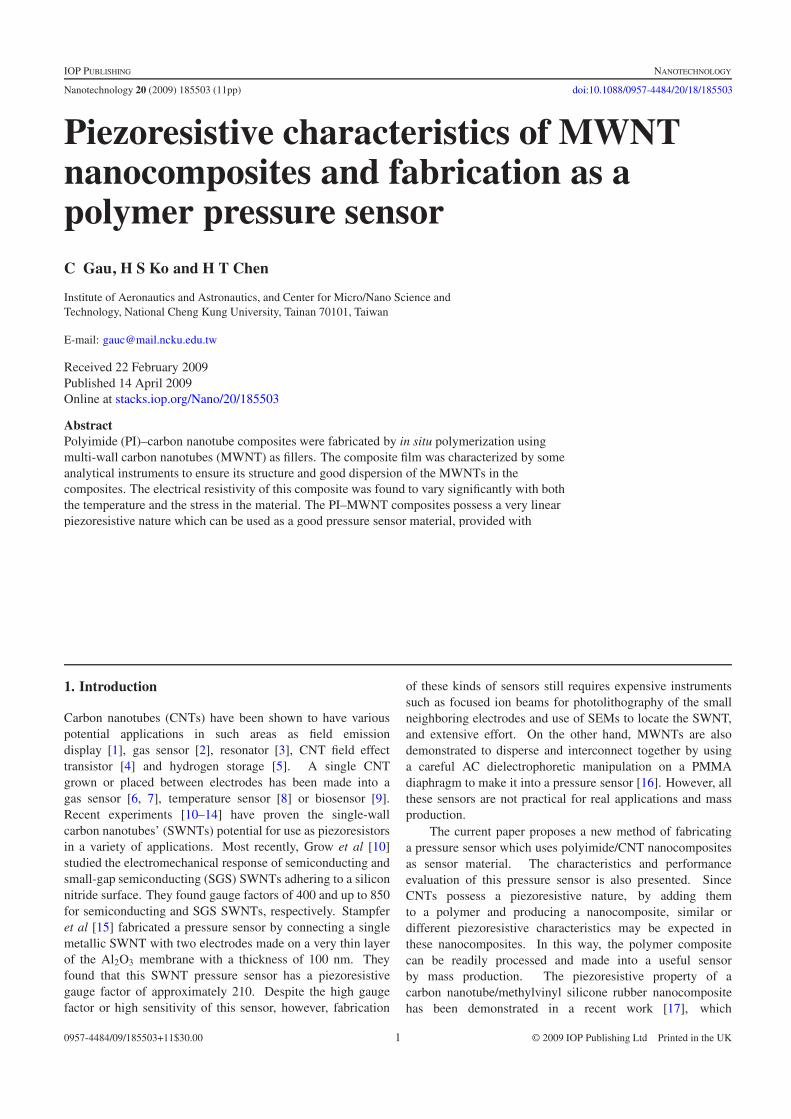
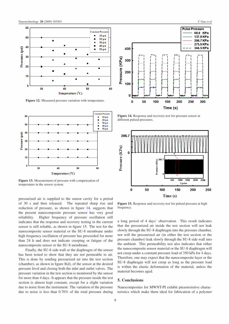
pressurized air is supplied to the sensor cavity for a periodof 30 s and then released. The repeated sharp rise andreduction of pressure, as shown in figure 14, suggests thatthe present nanocomposite pressure sensor has very goodreliability. Higher frequency of pressure oscillation stillindicates that the response and recovery testing in the currentsensor is still reliable, as shown in figure 15. The test for thenanocomposite sensor material or the SU-8 membrane underhigh frequency oscillation of pressure has proceeded for morethan 24 h and does not indicate creeping or fatigue of thenanocomposite sensor or the SU-8 membrane.
Finally, the SU-8 side wall or the diaphragm of the sensorhas been tested to show that they are not permeable to air.This is done by sending pressurized air into the test section(chamber), as shown in figure 8(d), of the sensor at the desiredpressure level and closing both the inlet and outlet valves. Thepressure variation in the test section is monitored by the sensorfor more than 4 days. It appears that the pressure inside the testsection is almost kept constant, except for a slight variationdue to noise from the instrument. The variation of the pressuredue to noise is less than 0.76% of the total pressure during
Figure 14. Response and recovery test for pressure sensor atdifferent pulsed pressures.
Figure 15. Response and recovery test for pulsed pressure at highfrequency.
a long period of 4 days’ observation. This result indicatesthat the pressurized air inside the test section will not leakslowly through the SU-8 diaphragm into the pressure chamber,nor will the pressurized air (in either the test section or thepressure chamber) leak slowly through the SU-8 side wall intothe ambient. This permeability test also indicates that eitherthe nanocomposite sensor material or the SU-8 diaphragm willnot creep under a constant pressure load of 350 kPa for 4 days.Therefore, one may expect that the nanocomposite layer or theSU-8 diaphragm will not creep as long as the pressure loadis within the elastic deformation of the material, unless thematerial becomes aged.
5. Conclusions
Nanocomposites for MWNT-PI exhibit piezoresistive charac-teristics which make them ideal for fabrication of a polymer
9
floayza
Rectángulo

Nanotechnology 20 (2009) 185503 C Gau et al
pressure sensor. As a sensor material, the linear variation ofthe film resistance with the pressure force of MWNTs–PI ismuch superior than the nonlinear behavior of MWNTs–siliconrubber. This suggests that the resistance of the compositesis dominated by the nanotubes, not the resistance in the gapwidth between neighboring MWNTs. A polymer pressure sen-sor has the advantages of a large area, low temperature, so-lution process which means low cost. In addition, the costfor the nanocomposite material with PI–MWNTs is also verylow in comparison with other conducting polymer materials.In addition, the polymer pressure sensor can be made flexible,which can be used for blood pressure measurements or othermedical applications. Fabrication of this kind of micropolymerpressure sensor has been presented. The fabrication processhas been completely simplified and the absence of the stic-tion problem, like the one which occurred in the polysiliconpressure sensor, has been noted. In addition, this kind of sen-sor can be readily integrated with a complicated microfluidicsystem for detailed flow information measurements. However,care should be taken in the cavity formation in the SU-8 layerand the release of the residual stress in the diaphragm. Perfor-mance evaluation of this sensor has also been provided, whichdemonstrates that the sensor is highly reliable.
References
[1] Wang Q H, Corrigan T D, Dai J Y and Chang R P H 1997 Fieldemission from nanotube bundle emitters at low field Appl.Phys. Lett. 70 3308–10
[2] Kong J, Franklin N R, Zhou C, Chapline M G, Peng S,Cho K and Dai H 2000 Nanotube molecular wires aschemical sensors Science 287 622–5
[3] Ghalkesar M, Barwich V, Lang H P, Braun T, Hegner M andGerber C 2004 Real-time mass sensing by nano mechanicalresonators in fluid Proc. IEEE Sensor (Dec. 2004)
[4] Tans S J, Verschueren A R M and Dekker C 1998Room-temperature transistor based on a single carbonnanotube Nature 393 49–52
[5] Dillon A C, Jones K M, Bekkedahl T A, Kiang C H,Bethune D S and Heben M J 1997 Storage of hydrogen insingle-walled carbon nanotubes Nature 386 377–9
[6] Zhang Y, Chang A, Cao J, Wang Q, Kim W, Li Y, Morris N,Yenilmez E, Kong J and Dai H 2001 Electric-field-directedgrowth of aligned single-walled carbon nanotubes Appl.Phys. Lett. 79 3155–7
[7] Qi P, Vermesh O, Grecu M, Javey A, Wang Q and Dai H 2003Toward large arrays of multiplex functionalized carbonnanotube sensors for highly sensitive and selective moleculardetection Nano Lett. 3 347–51
[8] Kuo C Y, Chan C L, Gau C, Liu C W, Hsiau S H andTing S H 2007 Nano temperature sensor using selectivelateral growth of carbon nanotube between electrodes IEEETrans. Nanotechnol. 6 63–9
[9] Im H, Huang X-J, Gu B and Choi Y-K 2007 Adielectric-modulated field-effect transistor for biosensingNat. Nanotechnol. 2 430–4
[10] Grow R J, Wang Q, Cao J, Wang D and Dai H 2005Piezoresistance of carbon nanotubes on deformable thin-filmmembranes Appl. Phys. Lett. 86 093104
[11] Cao J, Wang Q and Dai H 2003 Electromechanical propertiesof metallic, quasimetallic, and semiconducting carbonnanotubes under stretching Phys. Rev. Lett. 90 157601–4
[12] Tombler T W, Zhou C, Alexseyev L, Kong J, Dai H, Liu L,Jayanthi C S, Tang M and Wu S 2000 Reversibleelectromechanical characteristics of carbon nanotubes underlocal-probe manipulation Nature 405 769–72
[13] Minot E D, Yaish Y, Sazonova V, Park J-Y, Brink M andMcEuen P L 2003 Tuning carbon nanotube band gaps withstrain Phys. Rev. Lett. 90 156401–4
[14] Maiti A, Svizhenko A and Anantram M P 2002 Electronictransport through carbon nanotubes: effects of structuraldeformation and tube chirality Phys. Rev. Lett. 881268051–4
[15] Stampfer C, Helbling T, Obergfell D, Schoberle B, Tripp M K,Jungen A, Roth S, Bright V M and Hierold C 2006Fabrication of single-walled carbon-nanotube-based pressuresensors Nano Lett.6 233–7
[16] Fung C K M, Zhang M Q H, Chan R H M and Li W J 2005A PMMA-based micro pressure sensor chip using carbonnanotubes as sensing element MEMS 2005 (Miami):Technical Digest pp 251–4
[17] Dang Z M, Jian M-J, Xie D, Yao S-H, Zhang L-Q andBai J 2008 Supersensitive linear piezoresistive property incarbon nanotubes/silicone rubber nanocomposites J. Appl.Phys. 104 024114
[18] Jiang X, Bin Y and Matsuo M 2005 Electrical and mechanicalproperties of polyimide–carbon nanotubes compositesfabricated by in situ polymerization Polymer 46 7418–24
[19] Zhu B-K, Xie S-H, Xu Z-K and Xu Y-Y 2006 Preparation andproperties of the polyimide/multi-walled carbon nanotubes(MWNTs) nanocomposites Compos. Sci. Technol.66 548–54
[20] Lee G B, Lin C H and Chang G L 2003 Micro flow cytometerswith buried SU-8/SOG optical waveguides SensorsActuators A 103 165–70
[21] Ribeiro J C, Minas G, Turmezei P, Wolffenbuttel R F andCorreia J H 2005 A SU-8 fluidic microsystem for biologicalfluids analysis Sensors Actuators A 123/124 77–81
[22] Giordani N, Camberlein L, Gaviot E, Polet F, Pelletier N andBeche B 2007 Fast psychrometers as new SU-8 basedmicrosystems IEEE Trans. Instrum. Meas. 56 102–6
[23] Pelletier N, Beche B, Tahani N, Zyss J, Camberlein L andGaviot E 2007 SU-8 waveguiding interferometricmicro-sensor for gage pressure measurement SensorsActuators A 135 179–84
[24] Vilkner T, Janasek D and Manz A 2004 Micro total analysissystems. Recent developments Anal. Chem. 76 3373–86
[25] Trung N, Nguyen N and Wu Z 2005 Micromixer—a review J.Micromech. Microeng. 15 R1–16
[26] Monat C, Domachuk P and Eggleton B J 2007 Integratedoptofluidics: a new river of light Nature Photon. 1 106–14
[27] Juang Y H, Kuo C Y, Liu C W, Lin C H and Gau C 2009Functionalization of carbon nanotubes and formation ofnanocomposites with poly(ethylene terephthalate) withmeasurements of electrical and thermal conductivityCompos. Sci. Technol. submitted
[28] Core T A, Tsang W K and Sherman S J 1993 Fabricationtechnology for an integrated surface micromachined sensorSolid State Technol. 39–47 Author: [28]: Please providevolume number.
[29] Kim C J, Kim J Y and Sridharan B 1998 Comparativeevaluation of drying techniques for surface micromachiningSensors Actuators A 64 17–26
[30] Madou M J 2002 Fundamentals of Microfabrication 2nd edn(Boca Raton, FL: CRC Press) pp 276–7
[31] Boresi A P et al 1993 Advanced Mechanics of Materials (NewYork: Wiley) pp 538–9
[32] Guckel H 1991 Surface micromachined pressure transducerSensors Actuators A 28 133–46
10

Nanotechnology 20 (2009) 185503 C Gau et al
[33] Ko H S, Liu C W, Gau C and Yang C S 2007 Fabrication anddesign of a heat transfer micro channel system at lowtemperature MEMS technique J. Micromech. Microeng.17 983–93
[34] Stoney G G 1909 The tension of metallic films deposited byelectrolysis Proc. R. Soc. A 82 172–5
[35] Davidenkov N N 1961 Measurement of residual stresses inelectrolytic deposits Sov. Phys.—Solid State 2 2595–8 (Engl.Transl.)
[36] Finegan J D and Hoffman R W 1961 8th National Symp. onVacuum Technology Transactions (New York: Pergamon)p 935
[37] Ko H S, Liu C W and Gau C 2007 A novel fabrication forpressure sensor with polymer material and evaluation of itsperformance J. Micromech. Microeng. 17 1640–8
[38] French P J and Evans A G R 1984 Piezoresistance inpolysilicon Electron. Lett. 20 999–1000
11
floayza
Rectángulo