


ST_Vol_237_Sept_Oct_.. - International Frequency Sensor ...
188
-
Upload
khangminh22 -
Category
Documents
-
view
2 -
download
0
Transcript of ST_Vol_237_Sept_Oct_.. - International Frequency Sensor ...

SSeennssoorrss && TTrraannssdduucceerrss
IInntteerrnnaattiioonnaall OOffffiicciiaall OOppeenn AAcccceessss JJoouurrnnaall ooff tthhee IInntteerrnnaattiioonnaall FFrreeqquueennccyy SSeennssoorr AAssssoocciiaattiioonn ((IIFFSSAA))
DDeevvootteedd ttoo RReesseeaarrcchh aanndd DDeevveellooppmmeenntt ooff SSeennssoorrss aanndd TTrraannssdduucceerrss
VVoolluummee 223377,, IIssssuuee 99--1100 SSeepptteemmbbeerr--OOccttoobbeerr 22001199
Editor-in-Chief Prof., Dr. Sergey Y. YURISH
IFSA Publishing: Barcelona Toronto

Sensors & Transducers is an open access journal which means that all content (article by article) is freely available without charge to the user or his/her institution. Users are allowed to read, download, copy, distribute, print, search, or link to the full texts of the articles, or use them for any other lawful purpose, without asking prior permission from the publisher or the author. This is in accordance with the BOAI definition of open access. Authors who publish articles in Sensors & Transducers journal retain the copyrights of their articles. The Sensors & Transducers journal operates under the Creative Commons License CC-BY. Notice: No responsibility is assumed by the Publisher for any injury and/or damage to persons or property as a matter of products liability, negligence or otherwise, or from any use or operation of any methods, products, instructions or ideas contained in the material herein. Published by International Frequency Sensor Association (IFSA) Publishing. Printed in the USA.

SSeennssoorrss && TTrraannssdduucceerrss
Volume 237, Issue 9-10 September-October 2019 www.sensorsportal.com
e-ISSN 1726-5479 ISSN 2306-8515
Editors-in-Chief: Professor, Dr. Sergey Y. Yurish, tel.: +34 696067716, e-mail: [email protected]
Editors for Western Europe Meijer, Gerard C.M., Delft Univ. of Technology, The Netherlands Ferrari, Vittorio, Universitá di Brescia, Italy Mescheder, Ulrich, Univ. of Applied Sciences, Furtwangen, Germany
Editor for Eastern Europe Sachenko, Anatoly, Ternopil National Economic University, Ukraine
Editors for North America Katz, Evgeny, Clarkson University, USA Datskos, Panos G., Oak Ridge National Laboratory, USA Fabien, J. Josse, Marquette University, USA
Editor for Africa Maki K., Habib, American University in Cairo, Egypt
Editors South America Costa-Felix, Rodrigo, Inmetro, Brazil Walsoe de Reca, Noemi Elisabeth, CINSO-CITEDEF UNIDEF (MINDEF-CONICET), Argentina Editors for Asia Ohyama, Shinji, Tokyo Institute of Technology, Japan Zhengbing, Hu, Huazhong Univ. of Science and Technol., China Li, Gongfa, Wuhan Univ. of Science and Technology, China Editor for Asia-Pacific Mukhopadhyay, Subhas, Massey University, New Zealand
International Advisory Board
Abdul Rahim, Ruzairi, Universiti Teknologi, Malaysia Abramchuk, George, Measur. Tech. & Advanced Applications, Canada Aluri, Geetha S., Globalfoundries, USA Ascoli, Giorgio, George Mason University, USA Atalay, Selcuk, Inonu University, Turkey Atghiaee, Ahmad, University of Tehran, Iran Augutis, Vygantas, Kaunas University of Technology, Lithuania Ayesh, Aladdin, De Montfort University, UK Baliga, Shankar, B., General Monitors, USA Barlingay, Ravindra, Larsen & Toubro - Technology Services, India Basu, Sukumar, Jadavpur University, India Bousbia-Salah, Mounir, University of Annaba, Algeria Bouvet, Marcel, University of Burgundy, France Campanella, Luigi, University La Sapienza, Italy Carvalho, Vitor, Minho University, Portugal Changhai, Ru, Harbin Engineering University, China Chen, Wei, Hefei University of Technology, China Cheng-Ta, Chiang, National Chia-Yi University, Taiwan Cherstvy, Andrey, University of Potsdam, Germany Chung, Wen-Yaw, Chung Yuan Christian University, Taiwan Cortes, Camilo A., Universidad Nacional de Colombia, Colombia D'Amico, Arnaldo, Università di Tor Vergata, Italy De Stefano, Luca, Institute for Microelectronics and Microsystem, Italy Ding, Jianning, Changzhou University, China Djordjevich, Alexandar, City University of Hong Kong, Hong Kong Donato, Nicola, University of Messina, Italy Dong, Feng, Tianjin University, China Erkmen, Aydan M., Middle East Technical University, Turkey Fezari, Mohamed, Badji Mokhtar Annaba University, Algeria Gaura, Elena, Coventry University, UK Gole, James, Georgia Institute of Technology, USA Gong, Hao, National University of Singapore, Singapore Gonzalez de la Rosa, Juan Jose, University of Cadiz, Spain Goswami, Amarjyoti, Kaziranga University, India Guillet, Bruno, University of Caen, France Hadjiloucas, Sillas, The University of Reading, UK Hao, Shiying, Michigan State University, USA Hui, David, University of New Orleans, USA Jaffrezic-Renault, Nicole, Claude Bernard University Lyon 1, France Jamil, Mohammad, Qatar University, Qatar Kaniusas, Eugenijus, Vienna University of Technology, Austria Kim, Min Young, Kyungpook National University, Korea Kumar, Arun, University of Delaware, USA Lay-Ekuakille, Aime, University of Lecce, Italy Li, Fengyuan, HARMAN International, USA Li, Jingsong, Anhui University, China Li, Si, GE Global Research Center, USA Lin, Paul, Cleveland State University, USA Liu, Aihua, Chinese Academy of Sciences, China Liu, Chenglian, Long Yan University, China Liu, Fei, City College of New York, USA Mahadi, Muhammad, University Tun Hussein Onn Malaysia, Malaysia Mansor, Muhammad Naufal, University Malaysia Perlis, Malaysia
Marquez, Alfredo, Centro de Investigacion en Materiales Avanzados, MexicoMishra, Vivekanand, National Institute of Technology, India Moghavvemi, Mahmoud, University of Malaya, Malaysia Morello, Rosario, University "Mediterranea" of Reggio Calabria, Italy Mulla, Imtiaz Sirajuddin, National Chemical Laboratory, Pune, India Nabok, Aleksey, Sheffield Hallam University, UK Neshkova, Milka, Bulgarian Academy of Sciences, Bulgaria Pal, Jitendra, Carnegie Mellon University, USA Passaro, Vittorio M. N., Politecnico di Bari, Italy Patil, Devidas Ramrao, R. L. College, Parola, India Penza, Michele, ENEA, Italy Pereira, Jose Miguel, Instituto Politecnico de Setebal, Portugal Pillarisetti, Anand, Sensata Technologies Inc, USA Pogacnik, Lea, University of Ljubljana, Slovenia Pullini, Daniele, Centro Ricerche FIAT, Italy Qiu, Liang, Avago Technologies, USA Reig, Candid, University of Valencia, Spain Restivo, Maria Teresa, University of Porto, Portugal Rodríguez Martínez, Angel, Universidad Politécnica de Cataluña, Spain Sadana, Ajit, University of Mississippi, USA Sadeghian Marnani, Hamed, TU Delft, The Netherlands Sapozhnikova, Ksenia, D. I. Mendeleyev Institute for Metrology, Russia Singhal, Subodh Kumar, National Physical Laboratory, India Shah, Kriyang, La Trobe University, Australia Shi, Wendian, California Institute of Technology, USA Shmaliy, Yuriy, Guanajuato University, Mexico Song, Xu, An Yang Normal University, China Srivastava, Arvind K., Systron Donner Inertial, USA Stefanescu, Dan Mihai, Romanian Measurement Society, Romania Sumriddetchkajorn, Sarun, Nat. Electr. & Comp. Tech. Center, Thailand Sun, Zhiqiang, Central South University, China Sysoev, Victor, Saratov State Technical University, Russia Thirunavukkarasu, I., Manipal University Karnataka, India Thomas, Sadiq, Heriot Watt University, Edinburgh, UK Tian, Lei, Xidian University, China Tianxing, Chu, Research Center for Surveying & Mapping, Beijing, China Vanga, Kumar L., ePack, Inc., USA Vazquez, Carmen, Universidad Carlos III Madrid, Spain Wang, Jiangping, Xian Shiyou University, China Wang, Peng, Qualcomm Technologies, USA Wang, Zongbo, University of Kansas, USA Xu, Han, Measurement Specialties, Inc., USA Xu, Weihe, Brookhaven National Lab, USA Xue, Ning, Agiltron, Inc., USA Yang, Dongfang, National Research Council, Canada Yang, Shuang-Hua, Loughborough University, UK Yaping Dan, Harvard University, USA Yue, Xiao-Guang, Shanxi University of Chinese Traditional Medicine, China Xiao-Guang, Yue, Wuhan University of Technology, China Zakaria, Zulkarnay, University Malaysia Perlis, Malaysia Zhang, Weiping, Shanghai Jiao Tong University, China Zhang, Wenming, Shanghai Jiao Tong University, China Zhang, Yudong, Nanjing Normal University China
Sensors & Transducers journal is an open access, peer review international journal published monthly by International Frequency Sensor Association (IFSA). Available in both: print and electronic (printable pdf) formats.

SSeennssoorrss && TTrraannssdduucceerrss JJoouurrnnaall
CCoonntteennttss
Volume 237 Issue 9-10 September-October 2019
www.sensorsportal.com ISSN 2306-8515e-ISSN 1726-5479
Research Articles
Foreword to Special Issue Sergey Y. Yurish ................................................................................................................ I Opening Address to the 20 IFSA Anniversary –SEIA’ 2019, Adeje, Canary Islands (Tenerife), Spain, 25 – 27 September 2019 Dan Mihai Ştefanescu .......................................................................................................... 1 Monitoring of Hypohydration Caused by Physical Exercise Using a System-on-Chip-Based Bioimpedance Meter Vladimir Leonov, Mario Konijnenburg, Bernard Grundlehner and Nick Van Helleputte ..... 8 Novel Integrated Magnetic Sensor Based on Hall Element Array Janez Trontelj, Damjan Berčan, Miha Gradišek and Janez Trontelj ml. ............................. 17 Accurate Level Measurement Based on Capacitive Differential Pressure Sensing Parisa Esmaili, Federico Cavedo and Michele Norgia ......................................................... 23 Piezoelectric Ceramic Transducers as Time-Varying Displacement Sensors in Nanopositioners Massoud Hemmasian Ettefagh, Mokrane Boudaud, Ali Bazaei, Zhiyong Chen and Stéphane Régnier ......................................................................................................... 30 High Temperature Sapphire Optical Fiber Sensor Na Zhao, Qijing Lin,Zhuangde Jiang,Kun Yao, BianTian and Zhongkai Zhang .................. 37 Micro-structured Optical Spectrometer Sensor in PMMA Fischer-Hirchert Ulrich H. P., Höll Sebastian, Haupt Matthias and Joncic Mladen ............. 43 Calculation of Output Optical Signalsof Mechanoluminescent Impulse Pressure Sensors Konstantin Tatmyshevskiy ................................................................................................... 52 MIS Transistor with Integrated Waveguide for Electrophotonics and the Effect of Channel Length in Light Detection J. Hernández-Betanzos, A. A. González-Fernández, J. Pedraza and M. Aceves-Mijares .. 60 Optimized Integrated PIN Photodiodes with Improved Backend Layers Ingrid Jonak-Auer, Frederic ROGER and Olesia Synooka .................................................. 67 A Miniaturized Ultra Wide-band Band-pass Filter for the Tenerife Microwave Spectrometer Javier De Mguel-Hernández and Roger J. Hoyland ............................................................ 75 Novel and Cost-efficient Sensors for the Concentration Measurement of Ammonia and Ammonium Nitrate Particles Mohamed Lamine Boukhenane, Nathalie Redon, Jean-Luc Wojkiewicz, Caroline Duc and Patrice Coddeville ................................................................................... 80

The Measurement of Blood Coagulation Process in Extracorporeal Circuit Using LED Photoacoustic Imaging Takahiro Wabe, Ryo Suzuki, Kazuo Maruyama and Yasutaka Uchida .............................. 88 Micro-calorimetric Flow Rate Measurement Device for Microfluidic Applications Bilel Neji ............................................................................................................................... 95 Support Vector Machine Analysis to Detect Deviation in a Health Condition Monitoring System Yasutaka Uchida, Tomoko Funayama and Yoshiaki Kogure .............................................. 103 IndusBee 4.0 – Integrated Intelligent Sensory Systems for Advanced Bee Hive Instrumentation and Hive Keepers’ Assistance Systems Andreas König ...................................................................................................................... 109 Negative Ion Instrumentation for Detection of the Electron Affinity of Astatine Lars E. Bengtsson ................................................................................................................ 122 Fusion of Digital Road Maps with Inertial Sensors and Satellite Navigation Systems Using Kalman Filter and Hidden Markov Models Hamza Sadruddin and Mohamed M. Atia ............................................................................ 129 Molecular Dynamics Simulation on Formation of Ge Thin Film for Flexible Communication Devices Yoshiaki Kogure, Tomoko Funayama and Yasutaka Uchida .............................................. 137 ZigBee-Based Wireless Sensor Network for Environment Monitoring ZigBee Fuzheng Zhang, Weile Jiang,Qijing Lin,Hao Wu ................................................................. 144 Environmental Monitoring System Using Unmanned Aerial Vehicles and WSN Rosa Camarillo, Jorge Flores, Juana Camarillo,Juan Ramirez, Eduardo Padilla and Alfonso Valenciana ....................................................................................................... 150 New Approach to Optimization of Crop Production and Environment Protection Olga Chambers, Janez Trontelj, Jurij Tasic and Janez Trontelj jr. ..................................... 159 Evaluation Results of Testing of the Measuring Instruments Software O. Velychko, O. Hrabovskyi and T. Gordiyenko .................................................................. 165 Features of Calibration of Precision LCR Meters O. Velychko, S. Shevkun and M. Dobroliubova ................................................................... 171
Authors are encouraged to submit article in MS Word (doc) and Acrobat (pdf) formats by e-mail: [email protected]. Please visit journal’s webpage with preparation instructions:
http://www.sensorsportal.com/HTML/DIGEST/Submition.htm International Frequency Sensor Association (IFSA).

Sensors & Transducers, Vol. 237, Issue 9-10, September-October 2019, pp. I-II
I
Foreword to Special Issue
It is my great pleasure to introduce a new, dual issue
of Sensors & Transducers journal, Vol. 237, Issue 9-10, September-October 2019, entitled ‘Sensors and Transducers: Design & Applications’. This special issue contains selected and extended papers from the 5th International Conference on Sensors and Electronic Instrumentation Advances (SEIA' 2019), which has taken place on 25–27 September 2019, Adeje, Canary Islands (Tenerife), Spain.
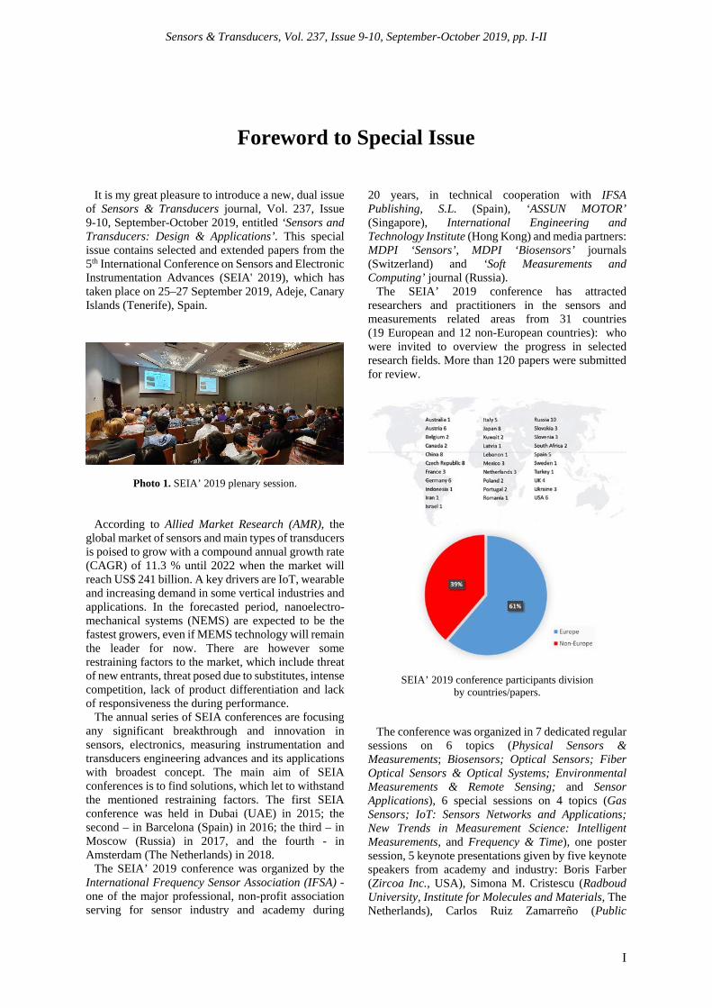
Photo 1. SEIA’ 2019 plenary session. According to Allied Market Research (AMR), the
global market of sensors and main types of transducers is poised to grow with a compound annual growth rate (CAGR) of 11.3 % until 2022 when the market will reach US$ 241 billion. A key drivers are IoT, wearable and increasing demand in some vertical industries and applications. In the forecasted period, nanoelectro-mechanical systems (NEMS) are expected to be the fastest growers, even if MEMS technology will remain the leader for now. There are however some restraining factors to the market, which include threat of new entrants, threat posed due to substitutes, intense competition, lack of product differentiation and lack of responsiveness the during performance.
The annual series of SEIA conferences are focusing any significant breakthrough and innovation in sensors, electronics, measuring instrumentation and transducers engineering advances and its applications with broadest concept. The main aim of SEIA conferences is to find solutions, which let to withstand the mentioned restraining factors. The first SEIA conference was held in Dubai (UAE) in 2015; the second – in Barcelona (Spain) in 2016; the third – in Moscow (Russia) in 2017, and the fourth - in Amsterdam (The Netherlands) in 2018.
The SEIA’ 2019 conference was organized by the International Frequency Sensor Association (IFSA) - one of the major professional, non-profit association serving for sensor industry and academy during
20 years, in technical cooperation with IFSA Publishing, S.L. (Spain), ‘ASSUN MOTOR’ (Singapore), International Engineering and Technology Institute (Hong Kong) and media partners: MDPI ‘Sensors’, MDPI ‘Biosensors’ journals (Switzerland) and ‘Soft Measurements and Computing’ journal (Russia).
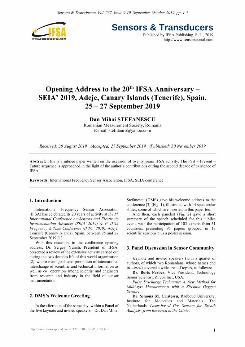
The SEIA’ 2019 conference has attracted researchers and practitioners in the sensors and measurements related areas from 31 countries (19 European and 12 non-European countries): who were invited to overview the progress in selected research fields. More than 120 papers were submitted for review.
SEIA’ 2019 conference participants division by countries/papers.
The conference was organized in 7 dedicated regular
sessions on 6 topics (Physical Sensors & Measurements; Biosensors; Optical Sensors; Fiber Optical Sensors & Optical Systems; Environmental Measurements & Remote Sensing; and Sensor Applications), 6 special sessions on 4 topics (Gas Sensors; IoT: Sensors Networks and Applications; New Trends in Measurement Science: Intelligent Measurements, and Frequency & Time), one poster session, 5 keynote presentations given by five keynote speakers from academy and industry: Boris Farber (Zircoa Inc., USA), Simona M. Cristescu (Radboud University, Institute for Molecules and Materials, The Netherlands), Carlos Ruiz Zamarreño (Public

II
University of Navarra, Institute of Smart Cities (ISC), Spain), José Miguel Dias Pereira (Polytechnic Institute of Setúbal, Portugal) and Dan Mihai Stefanescu (Romanian Measurement Society, Romania) and one panel dissuasion on IFSA activities, which has celebrate its 20th anniversary during the conference.
Photo 2. Poster Session at SEIA’ 2019 Conference. The MDPI ‘Biosensors’ open access journal
(ISSN 2079-6374) has announced the Best Paper Award (500.00 CHF), which was given to the authors of the best paper devoted to biosensors and presented at the SEIA' 2019 conference: ‘Portable Bioimpedance Device and Monitoring of Hydration in a Healthy Person Before and After Exercise’ written by Vladimir Leonov, Mario Konijnenburg, Hyunsoo Ha, Bernard Grundlehner and Nick Van Helleputte from Belgium and The Netherlands.
Photo 3. MDPI ‘Biosensors’ journal Award. Another two Awards were granted for the Best Paper
and Best Presentations at the special sessions on ‘IoT: Sensors, Networks and Applications’ to the authors of
the following papers: 1) ‘A flexible acoustic sensing system and its application to IoT – manufacturing field site’ written by Yasutaka Serizawa and Yusuke Shomura (Hitachi America, Ltd. R&D, IoT Edge Laboratory, USA); 2) ‘Concept for detection of device failures using active grid analysis’ written by Christina Sigl and Alexander Faschingbauer (Technical University Deggendorf, Germany).
I would like to thank all authors for submitting their latest work, thus contributing to the excellent technical contents of the journal.
A limited number of the best articles from this dual journal issue will be selected for extension into book chapters for publication in our popular open access Book Series ‘Advances in Sensors: Reviews’, Vol. 8 or ‘Advances in Measurements and Instrumentation: Reviews’, Vol. 2, which will be published in 2020/2021. Through the journal and book open access, the reach and impact of obtained and reported at the SEIA’ 2019 conference research results will be substantially increased.
Photo 4. Award Ceremony at SEIA’ 2019 conference.
The 6th International Conference on Sensors and
Electronic Instrumentation Advances (SEIA' 2020), will take place on 23-25 September 2020 in Porto, Portugal.
I hope you will enjoy this journal issue !
Sergey Y. Yurish Editor-in-Chief
Sensors & Transducers, Vol. 237, Issue 9-10, September-October 2019, pp. 1-7
1
Sensors & Transducers
Published by IFSA Publishing, S. L., 2019 http://www.sensorsportal.com
Opening Address to the 20th IFSA Anniversary – SEIA’ 2019, Adeje, Canary Islands (Tenerife), Spain,
25 – 27 September 2019
Dan Mihai ŞTEFANESCU Romanian Measurement Society, Romania
E-mail: [email protected]
Received: 30 August 2019 /Accepted: 27 September 2019 /Published: 30 November 2019 Abstract: This is a jubilee paper written on the occasion of twenty years IFSA activity. The Past – Present – Future sequence is approached in the light of the author’s contributions during the second decade of existence of IFSA. Keywords: International Frequency Sensor Association, IFSA, SEIA conference 1. Introduction
International Frequency Sensor Association (IFSA) has celebrated its 20 years of activity at the 5th International Conference on Sensors and Electronic Instrumentation Advances (SEIA’ 2019) & 1st IFSA Frequency & Time Conference (IFTC’ 2019), Adeje, Tenerife (Canary Islands), Spain, between 25 and 27 September 2019 [1].
With this occasion, in the conference opening address, Dr. Sergey Yurish, President of IFSA, presented a review of the extensive activity carried out during the two decades life of this world organization [2], whose main goals are: promotion of international interchange of scientific and technical information as well as cooperation among scientist and engineers from research and industry in the field of sensor instrumentation. 2. DMS’s Welcome Greeting
In the afternoon of the same day, within a Panel of the five keynote and invited speakers, Dr. Dan Mihai
Ştefănescu (DMS) gave his welcome address to the conference [3] (Fig. 1), illustrated with 14 spectacular slides, some of which are inserted in this paper too.
And then, each panelist (Fig. 2) gave a short summary of the speech scheduled for this jubilee event, with the participation of 103 experts from 31 countries, presenting 95 papers grouped in 13 scientific sessions plus a poster session.
3. Panel Discussion in Sensor Community
Keynote and invited speakers (with a quartet of authors, of which two Romanians, whose names end in ...escu) covered a wide area of topics, as follows:
Dr. Boris Farber, Vice President, Technology Senior Scientist, Zircoa Inc., USA:
Pulse Discharge Technique: A New Method for Multi-gas Measurements with a Zirconia Oxygen Sensor;
Dr. Simona M. Cristescu, Radboud University, Institute for Molecules and Materials, The Netherlands, Laser-based Gas Sensors for Breath Analysis: from Research to the Clinic;
http://www.sensorsportal.com/HTML/DIGEST/P_3103.htm

Sensors & Transducers, Vol. 237, Issue 9-10, September-October 2019, pp. 1-7
2
Dr. Dan Mihai Ştefănescu, Senior Scientist, Romanian Measurement Society, Romania,
Strain Gauges and Wheatstone Bridges in Multicomponent Force and Moment Transducers: Current Concepts and Applications;
Dr. Carlos Ruiz Zamarreño, Institute of Smart Cities (ISC), Public University of Navarra, Spain, Label-free Optical Fiber Sensing Platform Based on Lossy Mode Resonances;
Prof. José Miguel Dias Pereira, Polytechnic Institute of Setúbal, Portugal, A/D Conversion
Techniques Based on the Usage of Pulse Width Modulated (PWM) Signals: Applications for Digital Sensors and Sensor Systems.
In the slide in Fig. 3, I evoked IFSA achievements during the first 10 years (1999 – 2009), just like they were systematically arranged by Dr. Sergey Yurish in the centenary Issue of ‘Sensors & Transducers’ journal [4].
Fig. 1. First slide of the September 25, 2019 presentation, at the IFSA conference in Tenerife.
Fig. 2. Participants in the Panel from Sept. 25, 2019, at the IFSA conference in Tenerife.

Sensors & Transducers, Vol. 237, Issue 9-10, September-October 2019, pp. 1-7
3
Fig. 3. Self-explaining review in the first decade of activity of the International Frequency Sensor Association (Yurish S. Y., Sensors & Transducers, Vol. 100, No. 1, January 2009).
4. First DMS Paper for IFSA
The undersigned was honoured to take part in the IFSA publishings starting from 2011. The first published paper [5] was co-authored by my mentor, Dr. Aurel Millea (founder of the Romanian Measurement Society) (Fig. 4). Apart from the three specific representations (European – tree of knowledge, Asian – planetary system, and American –
subway map), reference is made to the general metrology science. In Fig. 4,b a comparison is shown of four ways of expressing Power, under Mechanical, Electrical, Chemical, and Thermo-Dynamic visions. The new SI, entered into force on May 20, 2019 (the World Metrology Day), is based on seven universal constants – see for details the second volume of my ‘Handbook of Force Transducers’ (Springer-Verlag).
Fig. 4. Copyright granted by IFSA for my ‘Handbook of Force Transducers’ (Volume 2) (a), for an image from the paper published in Sensors & Transducers journal in 2011 (b).

Sensors & Transducers, Vol. 237, Issue 9-10, September-October 2019, pp. 1-7
4
5. First DMS Conference and Book Chapter for IFSA
My first book chapter was published in 2016 within the IFSA Book Series [6], following the SEIA’ 2015 conference held in Dubai in 2015 (Fig. 5). There, I was the first Invited Speaker and presented the 1st volume of ‘Handbook of Force Transducers’ [7], and Dr. Amin Daneshmand Malayeri, Chairman of the Organizing Committee, exclaimed at the end of my speech: Brilliant!
I inserted (in Italics), in the title’s first part of this volume edited by Dr. Sergey Yurish, topics from my preferred area of interest: ‘Sensors (strain gauges), transducers (force), signal conditioning (Wheatstone bridges)’, with the mention “covering Electrical Measurement of Mechanical Quantities”! Continuity of this concern is also visible in the title of my SEIA’2019 conference [8], forming the basis of a chapter in the new volume ‘Advances in Sensors: Reviews’ Book Series 8 (in 2020).
Fig. 5. SEIA’2015 conference in Dubai (UAE): Dr. DMS (a) and the universal audience, meeting the “political correctness” requirements (b); Fragments of the volume cover [6] (c).
6. Second DMS Conference for IFSA
Main ideas developed in the Tenerife presentation on September 26, 2019, with 38 slides:
• Did you know that apart from resistive strain gauge there exist also capacitive, magnetoelastic, piezoelectric, SAW (surface acoustic wave), optical (Bragg grating, photoelastic or Fabry-Perot cavity) and “digital” (resonant cavity) ones?
• The original Wheatstone bridge was a group of four resistors connected in a bridge configuration, with a DC voltage supply in one of the diagonals and a null detector in another. Later on, this concept was extended to other bridge topologies: differential transformer (LVDT), magnetoresistive “bridge”, galvanomagnetic transducer (Hall-effect), and biparametric (R – L or L – C) half-bridge.
• Strain gauges and Wheatstone bridge represent the most wide-spread combination in achieving force transducers. One can take over from the finite elements programs the colour code for stressing elastic elements (red for tension and blue for compression) and adapt it to the bridge resistances (increasing and, respectively, decreasing).
• Did you think that in connection with multicomponent force and moment transducers there are certain confusions in terminology (sensor with transducer, torque with moment) and a regulation is not established for the coordinate axes representation (e.g. the “right hand screw rule”)?
• All these aspects will be discussed, starting with examples from materials testing, Robotics, aerodynamic balances for wind tunnels, and biomedical applications (e.g. TensoDentar equipment for virtual instrumentation).
7. Practical Accomplishments of the IFSA Companies
Ideas of presentations in these conferences (2015
and 2019) also show up in the outstanding practical achievements of the IFSA companies, fully confirming the slogan “Connecting Academy and Industry” in the title [2].
Since its founding in 2018, F2D, Ltd. (Ireland) – the IFSA Group Company, is continuing design and production of integrated circuits and sensor systems

Sensors & Transducers, Vol. 237, Issue 9-10, September-October 2019, pp. 1-7
5
solutions based on precision measurements of frequency-time parameters of signals [9].
The Universal Sensors and Transducers Interface (USTI) (Fig. 6) is a fully digital CMOS integrated circuit of universal, 2-channel, high precision, multifunctional converter with special function blocks
like RESISTANCE and RESISTIVE BRIDGE. It is remarkable the perfect agreement with the graphical symbolism proposed at the Tenerife conference [8] by DMS (acronym meaning in German DehnungsMessStreifen, i.e. in English “strain gauge”).
Fig. 6. Universal Sensors and Transducers Interface, innovation and industrial implementation on the market by company F2D, Ltd.
Combining the impeccable organization with the picturesque locations selected, social program offered at Hard Rock Hotel Tenerife at the end of the professional day was at the highest level: cocktail in Sky Lounge Bar, on the roof of Nirvana Tower building (24 September), banquet in Lagoon restaurant, near the Atlantic beach (26 September), and farewell party near the Wembley conference room (27 September 2019).
A line from George Harrison sits above the check-in area (Fig. 7). It reads: “Here comes the sun and I say, it’s all right!”, a fitting message for Hard Rock, which owns the largest rock memorabilia collection in the world [10].
8. First DMS Book for IFSA
It may be said that the International Frequency Sensor Association is a worldwide INTEGRATOR of experts, companies, products and publications. For my pleasure, there is a connection also with my professional evolution: Past – the 2011 paper, Present – the Tenerife conference, 2019 and Future – promising a DMS book at IFSA in 2020 (Fig. 8).
As Dr. Yurish mentioned in IFSA Publishing Book Catalog [11]: “Our authors, who are located around the world and whom we consider to be experts in their fields, write for practitioners, engineering and educational staff. This catalogue features all related publications and also includes bestsellers, handbooks and encyclopedias.”
Now, here’s that educational and encyclopedic topics are also present within the enlarged portfolio of IFSA titles! Where will you find 18 conference-touristic illustrated reports on all continents (without Antarctica)?
Dr. Dan Mihai Ştefănescu, in his book “Beyond Europe”, successfully builds a text rich in information and accompanied by spectacular images, offering a natural and inedited discourse on his experiences in exotic lands from Asia, America, Africa and Oceania. This journey agenda and, at the same time, intimate series of reports reflects the author’s impressions in his contacts with cultural environments much different from Europe, narrated in a fresh, ingenious, original and humorous style. In a multidisciplinary spirit, his book is full of historical, geographical, religious and economic information, presented with an unusual ability and easiness. Therefore, the reader feels like a direct participant in the world’s and life’s spectacle, as it develops at thousands of kilometers far from Europe (Dr. Aurel Millea in the foreword of the book).
Dear Dan, I personally have read your book
chapter (Dubai 2015) with a great pleasure! It is written well and interesting. I am also traveling a lot for different conferences (30 countries) and the topic is well known and useful for me (Dr. Sergey Yurish in [12]). 9. Conclusions
The paper reviews the rich palette of IFSA activities, over the two decades of fruitful existence. The next edition of the SEIA conference will be held at Porto, Portugal, in the autumn of 2020.
On my part, pleased by the increasing DMS publishing in connection with IFSA, conclude with a heart full wish: Long live IFSA!

Sensors & Transducers, Vol. 237, Issue 9-10, September-October 2019, pp. 1-7
6
Fig. 7. A Beatles song lyric in the check-in area of the Hard Rock Hotel in Tenerife (Credit: Roberto Lara) and triptych of images appearing in 2019, a bit blurred, like in a dream, and then fulfilled: DMS in Speakers’ Room Wembley (25 Sept.) (a), meeting… Paul McCartney (26 Sept.) (b), and at coffee break (27 September) with Mrs. Tetyana Zakharchenko, IFSA Conference & Publication Manager, and Prof. Dr. Sergey Yurish, Chairman of the Organizing Committee of SEIA’2019 (c).
Fig. 8. Crescendo of the DMS publishing activity at IFSA: paper in 2011 (+ this one in 2019) (a), book chapter in 2016 (+ one new in 2020) (b), and proposed book ‘Beyond Europe’ (c).
References [1]. 5th International Conference on Sensors and
Electronic Instrumentation Advances & 1st IFSA Frequency & Time Conference, Conference Programme, Adeje, Tenerife (Canary Islands), Spain, 25 – 27 September 2019, PDF created on 17 September 2019.
[2]. S. Y. Yurish, IFSA Activity report: Connecting Academy and Industry, Foreword, PDF created on 3 September 2019.
[3]. D. M. Ştefănescu, International Frequency Sensor Association Celebrating the 20th Anniversary in Canary Islands (Tenerife), Spain, 25 – 27 September 2019, Panel at Hard Rock Hotel, Adeje, Tenerife Island, 25 September 2019.
[4]. S. Y. Yurish, International Frequency Sensor Association (IFSA) Celebrates the 10th Anniversary, Sensors & Transducers Journal, Vol. 100, Issue 1, January 2009, pp. I-XII.
[5]. D. M. Ştefănescu, A. Millea, The Place of “Force” in Several Graphic Representations of the International

Sensors & Transducers, Vol. 237, Issue 9-10, September-October 2019, pp. 1-7
7
System of Units (SI), Sensors & Transducers, Vol. 131, Issue 8, August 2011, pp. 1-7.
[6]. D. M. Ştefănescu, Advances in Intelligent Force Transducers, in Sensors, Transducers, Signal Conditioning and Wireless Sensors Networks, in Advances in Sensors: Reviews (S. Y. Yurish, Ed.), Vol. 3, IFSA Publishing, Barcelona, 2016, pp. 21–36.
[7]. D. M. Ştefănescu, Handbook of Force Transducers – Principles and Components, 1st Edition, Springer-Verlag, Berlin, Heidelberg, 2011.
[8]. D. M. Ştefănescu, Strain gauges and Wheatstone bridges in multicomponent force / moment transducers – Current concepts and applications, Abstract in the Final Programme of the 5th International Conference on Sensors and Electronic
Instrumentation Advances (SEIA' 2019), Tenerife, Spain, 25 – 27 September 2019, pp. 8-9.
[9]. Universal Frequency-to-Digital Converter (UFDC) & Universal Sensors and Transducers Interface (USTI) ICs, Product Overview and Price List, F2D Catalog, PDF created on 4 June 2019.
[10]. A. Montgomery, Celebrate Live Music and Entertainment at the Hard Rock Hotel Tenerife, The Telegraph, 7 July 2017.
[11]. S. Y. Yurish, Publisher’s Letter, Book Catalog, IFSA Publishing, PDF created on 29 May 2019. http://www.sensorsportal.com/HTML/IFSA_Publishing.htm
[12]. S.Y. Yurish, private communication by e-mail, 30 December 2018.
__________________
Published by International Frequency Sensor Association (IFSA) Publishing, S. L., 2019 (http://www.sensorsportal.com).

Sensors & Transducers, Vol. 237, Issue 9-10, September-October 2019, pp. 8-16
8
Sensors & TransducersPublished by IFSA Publishing, S. L., 2019
http://www.sensorsportal.com
Monitoring of Hypohydration Caused by Physical
Exercise Using a System-on-Chip-Based Bioimpedance Meter
1 Vladimir LEONOV, 2 Mario KONIJNENBURG,
2 Bernard GRUNDLEHNER and 1 Nick Van HELLEPUTTE 1 Imec, Connected Health Solutions Belgium Department, Kapeldreef 75, 3001 Leuven, Belgium
2 Imec The Netherlands, Connected Health Solutions NL Department, High Tech Campus 31, 5656 AE Eindhoven, The Netherlands
1 Tel.: +3216288367, fax: +3216288500 E-mail: [email protected]
Received: 30 August 2019 /Accepted: 27 September 2019 /Published: 30 November 2019 Abstract: This paper describes accurate monitoring of hydration using impedance variation in a human being, which accompanies extracellular fluid loss or gain. A prototype of a precision multifrequency bioimpedance meter built around advanced biomedical SoC (System on Chip) MUSEIC v.2 was used in this study. Calibration of the bioimpedance board was conducted on an RC-model of the volunteer selected for the experiments. The model was built using the averaged results of multiple impedance measurements on the subject within the 1 Hz – 100 kHz, which were repeated on different days on near-euhydrated volunteer. The sources of observed variability in bioimpedance have been studied. Several factors were spotted that affect hydration assessment but were not reported in the literature before. The specific protocols for reaching fluid shift were developed in this study. They enabled minimization of errors in altered hydration state. The bioimpedance method is shown in this research to correctly reflect hydration variation in a single person, so that there is no need for averaging over large population to observe the trend. For demonstration of sensitivity of the developed device to fluid shift, it was tested on the volunteer undergoing repeated mild dehydration and rehydration using light-effort exercise (outdoor cycling). The bioimpedance results were compared with the reference hydration. The latter was obtained using the subject weight measurement and precise counting of caloric intake, the weight of food, and also with the aid of established weight baseline prior to any planned experiment. Special attention has been paid to sodium balance, and several diets have been developed for its regulation. The predictable body fluid loss and gain was supported by measured sweating rate, and also by dehydration and rehydration diets designed for precise control of ion and water intake. The accuracy of fluid shift measurement down to a standard deviation of 200 ml is demonstrated, which essentially exceeds capabilities of known methods and devices, including ‘gold standards’ like isotope dilution for hydration assessment. Such accuracy satisfies requirements of healthcare and sport. The device has not yet been validated on population. Keywords: Hydration, Hypohydration, Dehydration, Rehydration, Bioimpedance, System on chip, Human being. 1. Introduction to Hydration
Maintaining proper hydration is important for all living things. Almost two thirds of the weight of the
authors of this article is water. But if just a few percent of the body’s water were lost due to dehydration or insufficient water intake, it would already be difficult for them to concentrate and write a good article. An
http://www.sensorsportal.com/HTML/DIGEST/P_3104.htm
Sensors & Transducers, Vol. 237, Issue 9-10, September-October 2019, pp. 8-16
9
assessment of total body water (TBW) in an individual is not precise because of the wide variety in body build and composition [1 – 4]. Thus, the percentage of hypohydration and hyperhydration is estimated in respect to body weight. A dehydration by 3 to 6 % already create problems and the number of symptoms increases starting with thirst. Such dehydration corresponds to about 5 to 10 % loss of TBW, which must be compensated by fluid intake. However, drinking itself could also become dangerous for a dehydrated person. If large volumes of pure water are consumed in a short time, dilution of body fluids can lead to death, and such cases have been reported. Therefore, both proper hydration and optimum ion intake are vital for health and optimal physical and mental performance.
The TBW can be divided in two volumes: intracellular water (ICW) and extracellular water (ECW). The most accurate classical methods for fluid assessment are based on isotope dilution for TBW, total-body potassium (TBK) using γ-ray emission for ICW, and NaBr dilution for ECW. These methods are direct and called “gold standards”, although there are always some assumptions made, i.e., they all have intrinsic errors [2, 5 – 8]. Their accuracy was not measured directly as far as there was no better reference method, except TBW on small animals compared with their desiccation, where standard deviation (SD) of 3 % was observed while some researches showed larger discrepancies in TBW assessment [7, 8]. Although administration of radioactive tracers enables TBW evaluation, it does not allow repetitive assessments of TBW often required in the clinical settings. Comparison of a sum of ICW and ECW in humans (obtained by TBK and bromide dilution methods) with TBW obtained by D2O dilution showed that TBW, and thus hydration could be estimated with SD of about 4 l [5]. This actually means that a 99.73 % confidence interval (CI) defined as ±3SD extends up to about ±12 liters while TBW in a typical 70 kg man is of the order of 42 l [9]. Ref. [9] mentions accuracy for TBW of up to 5 % that corresponds to 99.73 % CI of about ±6 liters, i.e. two-fold better than measured in [5]. People working in hot environment, workers having heavy physical load and sportsmen can rapidly lose several liters of water if they do not drink on time. For the other healthy people, daily variation of weight within the 1.5 kg and of hydration within one liter is usual in a moderate climate (as observed in this research) while a two-liter dehydration (about 3 %) has already profound effect on physical and mental performance of a person. In this study, a typical nocturnal dehydration of 0.63 l was observed in a 72 kg man, which increased to 0.8 l at high nocturnal ambient temperatures, which is normal. Because of such natural diurnal variability, a precision of ±1 liter for hydration is widely assumed to be the ultimate goal for developers of new methods and devices for hydration assessment [10].
2. Modern Methods for Hydration Assessment
Hydration assessment is usually being conducted using a set of hydration indices (such as weight variation, urine osmolarity, its color and volume, skin elasticity) and symptoms (such as edema, mouth dryness, confusion, dizziness, tachycardia, thirst, fainting when standing up, headache, tiredness), blood test (plasma osmolarity and sodium), or, sometimes, using isotope dilution, etc. Among the methods, there are direct ones (blood tests, direct ECW sample and body weight change), those called gold standards that use some calculations (isotope and bromide dilution, TBK), and indirect methods (all others). The methods themselves and their combinations still lack precision [5, 9, 11 – 13].
Bioimpedance methods have been widely studied in application to estimation of body composition [4, 14]. The methods are based on total body water (TBW) calculation. The latter, in turn, is obtained using one of known regression equations, measured impedance of human body, and biometric data of the subject. Several regression equations were obtained for a normally hydrated general population and also for population-specific cases, see, e.g., [4]. The bioimpedance analysis (BIA) is indirect method for TBW assessment, it is quick and much easier than the classic methods used in medicine. The accuracy of bioimpedance methods compared to the “gold standards” is not better than the latter [15, 16]. However, they drastically simplify the hydration assessment and therefore are widely used, e.g., by dietologists, although the validity of conclusions based solely on the BIA is uncertain. This statement is supported by the CI reported in previous section for gold standards. It is also supported by the fact that bioimpedance methods are rarely used in clinics and never in critical situations. As reported, the CI is too large for clinical purposes [17], and that the TBW, ICW and ECW are consistent on population, but not at the individual level [18].
The rate of publications on bioimpedance methods approaches 1 paper per day [19] including this article. So far, none of researches has shown accuracy sufficient for using it in clinical practice [15 – 20]. Despite insufficient accuracy, bioimpedance methods were studied in application to hemodialysis [10, 18], where an accuracy of 1 liter would also be desirable [10]. When bioimpedance methods are used for measuring dynamic shifts in hydration, one could expect better accuracy of such relative bioimpedance variation. However, the diagnostic accuracy does not allow such relative measurements to be trusted either 5, 18, 20, 21]. For example, [22] concludes that the bioimpedance method does not provide a valid estimate of the change in TBW due to isotonic fluid loss, [23] reports that it was not valid under conditions of altered hydration, while [24] underlines that it is not

Sensors & Transducers, Vol. 237, Issue 9-10, September-October 2019, pp. 8-16
10
currently able to identify type and magnitude of fluid loss.
The bioimpedance regression equations obtained on the euhydrated population are not suited for the case of altered hydration. Therefore, it is not surprising that a lack of proof can be found in the literature that bioimpedance methods can assess hydration change with no need for averaging over the population. In addition to demonstrated nice statistical studies, there is a strong demand for any measurement device and method to assess TBW shift in a single healthy person, or in ambulatory application with an accuracy of about ±1 liter. The situation in hydration assessment methods is summarized, e.g., in [25]: “As of now, there are no reliable tools to determine hydration status.” This work is devoted to demonstration of accurate TBW shift measurement with accuracy better than the one of “gold standards” to such a shift. The presented method is relative, it shows variation of hydration relative to the baseline.
3. The Bioimpedance Sensor, its Calibration and the Measurement Setup
The early hydration monitoring studies at Imec [26] were conducted using commercial bioimpedance analyzers, lock-in amplifiers and earlier versions of wearable bioimpedance sensors [27, 28]. They have indicated the need for a more accurate device, adjustment of the measurement protocol and deeper understanding of the bioimpedance variability for better assessment of hydration status. In this work, the evaluation test board, Fig. 1, was built using one of the most advanced multiparameter signal acquisition System-on-Chip (SoC) MUSEIC v.2 for personal health applications [29, 30]. The chip with a size of 8 mm × 7 mm contains ten readout channels with the state-of-the-art accuracy, Fig. 2.
Fig. 1. Multiparameter signal acquisition test board built around SoC MUSEIC v.2.
In this work, only the multifrequency bioimpedance channel and the current generator were used. The bioimpedance sensor was used at selected
frequencies of 8, 16, 32, 64, 128, and 256 kHz at a current of 10 μA. A low-pass digital finite element response (FIR) filter selectable from 10 Hz to 150 Hz was used at 10 Hz. Variable current and gain enable selection of the most advantageous combination of sensitivity and dynamic range, depending on electrode locations on the human body. The 5-electrode configuration consists of two current electrodes, two potential electrodes, and a body bias electrode (to increase system stability and to reduce motion artifacts).
Fig. 2. MUSEIC v.2 SoC containing sensor readouts, filters, controller, and data analysis modules. Abbreviations denote current generator (CG), and readout channels for: galvanic skin response (GSR), photoplethysmography (PPG), a fixed-frequency (20 or 40 kHz) bioimpedance (BIOZ), a multifrequency bioimpedance (BIOZ-MF) within the 1 kHz to 1 MHz range. There are also three electrocardiography (ECG) and three reconfigurable (RECONF) channels that can be configured to any of readout channels mentioned above.
In this study, two basic electrode configurations
were used. The first one is a classical one, with tab electrodes between the wrist and ankle, for measuring in a supine position of the subject. However, given that the device should be wearable (after miniaturization), the forearm-to-forearm configuration was mainly used in this study. The Meditrace 200 wet-gel i- and v-electrodes on the forearm were separated by at least 9 cm, otherwise the required accuracy could not be achieved.
For characterization of the bioimpedance sensor, the selected volunteer’s electrical properties between the forearms and the properties of the electrode-skin pair have been repeatedly measured using EG&G 5210 lock-in amplifier within the 1 Hz – 100 kHz range for several days, averaged, and the electrical RC-model shown in Fig. 3 was obtained. It was used for calibration of the device and measurement of the system accuracy.

Sensors & Transducers, Vol. 237, Issue 9-10, September-October 2019, pp. 8-16
11
Fig. 3. Empiric RC-model of the male subject selected for the study in this work (top) and of electrode-skin pair (bottom) both suitable for 1 Hz – 128 kHz range. Typical R1 in euhydrated state was 200 Ω, and C1 was 22 nF. The range for RC-values was used for the device calibration.
The impedance of electrode-skin pair is highly
variable depending on sweating rate and skin blood flow. On average, at indoor temperatures and typical sedentary activity in the office, i.e., with no sweating, the impedance of Meditrace 200 wet-gel electrode and skin of the subject was modeled using the circuit shown in Fig. 3, top. For calibration of the bioimpedance sensor and system characterization, all five electrodes shown in Fig. 3, top, were replaced with the electrode-skin circuit shown in Fig. 3, bottom. At integration time of 16 s, a SD of resistance measured on the RC-model at 64 kHz was 45 mΩ. Therefore, in absence of human-related variability, the board is sensitive enough to detect body fluid change of about 50 ml with almost 100 % probability, because resistance variation in man exceeds 6SD at such fluid shift.
4. Euhydration Baseline, the Reference Method for Hydration Estimation, and the Rate of Fluid Loss in Exercise
The impedance of a healthy and normally hydrated person fluctuates throughout the day near its stable average [26]. The human body loses water and ions through insensible perspiration, sweating, urine and feces. However, they are renewed on a regular basis through food and water intake. But before the ions from food reach the cardiovascular system, the body must secrete about one to two liters of digestion fluids. Despite the presence of many other factors affecting the results, a variation of bioimpedance associated with food intake was detected by averaging multiple measurements before and after food intake for several days using commercially available Maltron BioScan
920 bioimpedance analyzer (on earlier stages of this work, when the test board was not yet ready). The impedance was measured at 5, 50 and 100 kHz in two setups, in supine position with tab electrodes on left wrist and ankle, and between forearms while standing. The trendline for left ankle-wrist plot correlated well with the trendline for wrist-to-wrist results [31]. The peak of impedance corresponded to about 30 – 60 min after meals. This is the time when digestion fluid is secreted, thereby increasing body impedance, but electrolyte from food is not yet fully absorbed.
Apart of food intake there are other factors that lead to a change in impedance in a healthy person. The measurements show that if a person takes a supine position, the impedance drift is observed for 20 min and more after that moment [26]. Therefore, in this study, the bioimpedance measurements on a standing, or sitting subject were preferable. Although these positions do not improve repeatability of the measurements, they are more appropriate for wearable applications. Conductivity of electrolytes, including body fluids, increases with temperature [32]. Therefore, care has been taken to keep extremities warm, although skin temperature was not constant. Soft human tissue is a soft material by definition. It is therefore impossible to ideally reproduce the body shape. Even in supine position, the impedance meter was sensitive to tiny repositioning of limbs.
Replacement of electrodes also affects the impedance because of positioning accuracy. For accurate electrode positioning, marking of electrode location with a marker was not good enough. The tiny body landmarks were used instead to have positioning accuracy within 1 mm. Depending on particular electrode location, a 2 mm-shift of two v-electrodes may cause impedance variation equivalent up to 0.5 l of body fluid change. Insensible bending of limbs also affects impedance. It can be controlled in a better way in a sitting or standing subject, e.g., using a forearm support and fixed places for feet.
Cables connecting body with the device also introduce errors. The cable-to-body and cable-to-cable crosstalk is observed while using ECG leads. Such cables are however soft and work well if care is taken about separation of them from the body. However, when standard coaxial cables were used, it was found that they are too rigid and heavy for soft human tissue. They pull skin and relocate the electrode-skin couple in respect to underlying tissue thereby producing an error, and sometimes a large error.
The bioimpedance analyzers are sensitive, to certain extent, to the electrode-skin pair impedance. The difference in electrode-skin impedances between electrodes (both v- and i-electrodes) also affects the results. Therefore, the results obtained using commercial bioimpedance analyzers are influenced by the electrode-skin impedance variation. Although variations are small, they have profound influence on measurement accuracy. The high input impedance of the developed board makes it immune to this effect.
Among other factors to be accounted for, sodium intake, sweating rate and increased blood flow in

Sensors & Transducers, Vol. 237, Issue 9-10, September-October 2019, pp. 8-16
12
exercising muscles are the most important factors. Therefore, while using cycling in this work for dehydration, the forearm-to-forearm electrode configuration was typically used to avoid drop of impedance in legs. Finally, lactate increase, despite relatively low input in ECW conductivity, also causes decrease of the impedance during and after exercise. In this work therefore high-effort exercise was prohibited, at least for the last 1 – 2 hours of cycling.
Because of natural daily impedance variability, establishing its baseline is important for detection of small changes related to hydration. Fig. 4 illustrates typical joint effect of the aforementioned factors in a normally hydrated person. Important that uncorrelated impedance between different parts of the body, Fig. 5, observed in everyday life clearly indicates errors in impedance measurements. Indeed, hydration affects the whole body, so that the results must be correlated.
Fig. 4. Weight (squares) and impedance in a healthy person monitored in a course of three days. Shown points is impedance averaged over 5, 50, 100 and 200 kHz between forearms (circles, solid line) and between the wrist and ankle (triangles, dotted line). Measured using commercially available bioimpedance analyzer.
Fig. 5. Independence of resistance between forearms on resistance between wrist and ankle. Shown experimental points is impedance averaged over 5, 50, 100 and 200 kHz. Measured using commercially available bioimpedance analyzer. A part of data points is taken from Fig. 4.
Fig. 4 also illustrates daily weight variation. Using weight as a reference for fluid shift monitoring was
adopted in this work. Impedance changes were compared with this direct method for hydration assessment. It is based on weight monitoring and calculation of fluid and food intake, balanced with energy expenditure. This made it possible to obtain a reference estimate of hydration with an accuracy of about 200 ml, which is better than could be obtained using other methods. The reference method however works only in a course of several days.
To monitor hydration, a man weighing 72 kg was selected. According to several regression equations for TBW, both anthropometric and bioimpedance, the studied man had 41.0 l of TBW in euhydrated state (averaged over ten equations). Maintaining proper hydration is known to be important in heat stress for both health and safety. Therefore, simulating the workload by cycling was performed this study at moderate to high ambient temperatures. The study followed the guidelines of the protocol Stress in the Work Environment approved by the Medical Ethical Committee of KUL Hospital. Cycling for several hours at the same effort provided near-constant physical load with measured average sweating rates based on weight loss. Fig. 6 shows experimental results on fluid loss, which enabled planning of the exercise duration depending on weather conditions and the target hypohydration level. Using these results, the sweat loss was predicted for every exercise, which allowed preparation of specific diets with required deficit or excess of sodium ions in respect to optimum intake. The scattering of points observed in Fig. 6 can be explained by difference in solar radiation, clouds and humidity, and slightly different cyclist performance depending on weather.
Fig. 6. Experimental rate of fluid loss depending on ambient temperature in the cyclist at a metabolic rate of 5±1 MET in his several usual tracks of 40 to 60 km long. The points mark average fluid loss in 18 exercises.
5. Diets with Known Ion Content for Predictable Fluid Shift The study preceding this project [26] has shown
that uncontrolled consumption of sodium (too much table salt in food consumed in chaotic manner) resulted in dramatic daily variation of ions and water

Sensors & Transducers, Vol. 237, Issue 9-10, September-October 2019, pp. 8-16
13
retention in the body. Accounting for unbalanced (ad libitum) food intake in respect to energy expenditure, these factors typically create large variations in both subject weight and his/her impedance. Therefore, the protocol included matched diets with precise quantity of potassium and sodium per day. Furthermore, while the subject was undergoing dehydration, the sodium intake was minimized, but it was doubled during rehydration. The latter provided faster rehydration compared to using balanced sodium intake.
As an example of developed diets, the menu for exercise day included rice, potato and pasta, chocolate bars, butter, all with no added salt, apple and grape juices, tomatoes, sugar, coffee, sunflower seeds, an apple and water (50 mg sodium and 3.6 – 6.0 g potassium intake per day, per 3700 kcal). Depending on duration of exercise, the menu was corrected to match energy expenditure. Fully balanced diets have sometimes been used to stabilize impedance before exercise and after rehydration. For example, one of such diets contained bread (salted and unsalted), potatoes, cheese (Gouda), eggs, tomatoes, beef, jam, garlic (one clove), soup (curry), milk, red wine, coffee, water (3.0 g sodium and 4.64 g potassium intake per day, per 2550 kcal).
For rehydration, it is necessary to drink 50 % more water than was lost. Rehydration diet contained between 150 to 220 % of recommended sodium intake per day thereby enabling better water retention and rapid rehydration. This enabled complete fluid recovery in just one day. As an example, the rehydration diet included bread (salted), potatoes, cheese (Gouda), eggs, ham, tomatoes, sausage (turkey), sugar, table salt, jam, garlic (one clove), soup (chicken), red wine, milk, coffee, water (6.7 g sodium and 4.3 g potassium intake per day, per 2550 kcal).
6. Dehydration and Rehydration Study, the Protocols and Results Hypohydration was provided by the combined
effect of limited water intake during 2 – 3 days and 1 – 2 days of cycling in warm/hot weather for 40 – 50 km distance at about 5±1 MET light effort. Low-sodium diet helped to decrease thirst and promoted water rejection. The impedance measurements were conducted on a sitting or standing subject between forearms to avoid measurements on exercising muscles (legs) of cyclist. Fig. 7 shows variation of both resistance at 64 kHz and the reference hydration of the subject during the week-long dehydration and rehydration experiment. The following protocol was used in this experiment. On first two days, a baseline of impedance was monitored together with the subject weight. Having euhydration baseline established using the average weight, it becomes possible to calculate hydration status using the subject’s weight and accounting for food and water intake. Regulation of hydration began on the third day, when a balanced diet accompanied by reduced water intake enabled initial slight hypohydration. On days
4 and 5, the no-Na+ diet was applied with reduced water intake, and cycling was used for faster dehydration. The rehydration started on fifth day, after exercise and a few measurements in hypohydrated state. The rich-Na+ diet was used and continued on the sixth day. As mentioned in previous section, about 150 % of water was consumed on the evening of the fifth day, and on the sixth day compared with the loss of water. On the seventh day, a balanced Na+ diet was used for fluid balance stabilization and equalization. Water intake on the seventh day was ad libitum. This or similar protocol was used in several experiments.
Fig. 7. Resistance between forearms at 64 kHz (circles) and the reference hydration based on weight and food intake (crosses) of a subject undergoing dehydration on days 3 to 5, cycling exercises on days 4 and 5, and rehydration on day 5 (after the 2nd exercise) and on day 6.
The results shown in Fig. 7 are still noisy, i.e., there
are some impedance variations apart of those caused by fluid shift. Accounting for imperfect calculation of hydration from weight and intake, a digital low-pass FIR filter was applied to both sets of data, resistance and hydration. A simple FIR filter or just a 3-point moving average offered about the same improvement. The result of such noise reduction is shown in Fig. 8. The result of a similar processing of reactance data is shown in Fig. 9 for the same experiment.
Fig. 8. Resistance between forearms at 64 kHz (circles) and the reference hydration (crosses). A low-pass filter (3-point moving average) is applied to both resistance and the reference hydration.
Sensors & Transducers, Vol. 237, Issue 9-10, September-October 2019, pp. 8-16
14
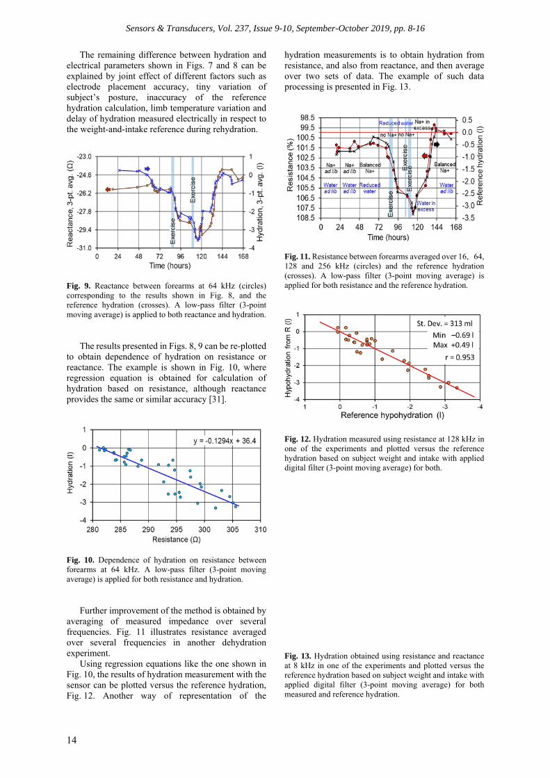
The remaining difference between hydration and electrical parameters shown in Figs. 7 and 8 can be explained by joint effect of different factors such as electrode placement accuracy, tiny variation of subject’s posture, inaccuracy of the reference hydration calculation, limb temperature variation and delay of hydration measured electrically in respect to the weight-and-intake reference during rehydration.
Fig. 9. Reactance between forearms at 64 kHz (circles) corresponding to the results shown in Fig. 8, and the reference hydration (crosses). A low-pass filter (3-point moving average) is applied to both reactance and hydration.
The results presented in Figs. 8, 9 can be re-plotted to obtain dependence of hydration on resistance or reactance. The example is shown in Fig. 10, where regression equation is obtained for calculation of hydration based on resistance, although reactance provides the same or similar accuracy [31].
Fig. 10. Dependence of hydration on resistance between forearms at 64 kHz. A low-pass filter (3-point moving average) is applied for both resistance and hydration.
Further improvement of the method is obtained by averaging of measured impedance over several frequencies. Fig. 11 illustrates resistance averaged over several frequencies in another dehydration experiment.
Using regression equations like the one shown in Fig. 10, the results of hydration measurement with the sensor can be plotted versus the reference hydration, Fig. 12. Another way of representation of the
hydration measurements is to obtain hydration from resistance, and also from reactance, and then average over two sets of data. The example of such data processing is presented in Fig. 13.
Fig. 11. Resistance between forearms averaged over 16, 64, 128 and 256 kHz (circles) and the reference hydration (crosses). A low-pass filter (3-point moving average) is applied for both resistance and the reference hydration.
Fig. 12. Hydration measured using resistance at 128 kHz in one of the experiments and plotted versus the reference hydration based on subject weight and intake with applied digital filter (3-point moving average) for both.
Fig. 13. Hydration obtained using resistance and reactance at 8 kHz in one of the experiments and plotted versus the reference hydration based on subject weight and intake with applied digital filter (3-point moving average) for both measured and reference hydration.

Sensors & Transducers, Vol. 237, Issue 9-10, September-October 2019, pp. 8-16
15
7. Discussion Hydration in this study was successfully monitored
at all studied frequencies, from 8 to 256 kHz, although the regression equations for dehydration, as clear from the RC-model, depend on frequency. For example, the slope of resistance change was 2.9 %/l at 16 kHz, and 2.3 %/l at 128 kHz. The best results were obtained so far using resistance at frequencies below 256 kHz and using reactance at low frequencies of 8 to 16 kHz, and also using averaging over hydration obtained separately using resistance and reactance. Application of data filtering, e.g., using a FIR filter, enabled further improvement of signal-to-noise ratio, where signal is hydration and noise is device-, electrode- and posture-related errors in the impedance of the subject.
Several factors were observed that usually cause instability of impedance. Among them, it is necessary to stress on variability of sodium intake, which is related to heavily salted food products available in grocery stores. Some of our initial experiments failed because volunteers consumed uncontrolled amount of cheese and ham between the measurements thereby creating chaotic electrolyte volume variation. As a result, water retention was affected, and the impedance fluctuated making hydration baseline noisy. The posture of the subject is not exactly reproduced from one measurement to another, and this is one of important factors introducing errors. Commercial impedance meters are frequently sensitive a little to electrode and skin impedances. In this relation, the body bias electrode, high CMRR (>100 dB) and high input impedance (2 GΩ) implemented in the developed device helped to eliminate some of errors observed in bioimpedance meters on the market.
The minimum SD of 200 ml for hydration variation observed in this work is seemingly largely affected by imperfect reference calculation of hydration based on food intake and weight of the subject. Indeed, the accuracy of the reference hydration was almost the same, with SD of about 100 – 150 ml on estimate, and the balance had a resolution of 100 g.
8. Conclusion
It is shown that the bioimpedance board with MUSEIC v.2 SoC enables accurate hydration monitoring in a healthy subject under condition of following a diet-based protocol. The achieved accuracy exceeds accuracy of the methods usually used for hydration shift assessment by at least a factor of ten. The method still needs both deeper studying and further validation on population. Of course, the measurement protocol and diets, which were necessary in this study for calibration of the device, could be simplified in the future for approval in hospitals and sport. Recently, a miniaturized wearable version of the device used in this work was presented [33], although it has not yet been tested as a wearable hydration monitor.
Acknowledgements
The authors are thankful to L. Hons (Premed, Leuven, Belgium) for providing medical surveillance and to C. Van Hoof (Imec) for enthusiasm, fruitful discussions, and useful suggestions.
References [1]. P. E. Watson, I. D. Watson, and R. D. Batt, Total body
water volumes for adult males and females estimated from simple anthropometric measurements, The American Journal of Clinical Nutrition, Vol. 33, 1980, pp. 27-39.
[2]. D. A. Schoeller, E. van Santen, D. W. Peterson, W. Dietz, J. Jaspan, and P. D. Klein, Total body water measurement in humans with 18O and 2H labeled water, The American Journal of Clinical Nutrition, Vol. 33, 1980, pp. 2686-2693.
[3]. E. C. Hoffer, C. K. Meador, and D. C. Simpson, Correlation of whole-body impedance with total body water volume, Journal of Applied Physiology, Vol. 27, Issue 4, 1969, pp. 531-534.
[4]. U. G. Kyle, I. Bosaeus, A. D. De Lorenzo, P. Deurenberg, et al., Bioelectrical impedance analysis — part I: review of principles and methods, Clinical Nutrition, Vol. 23, 2004, pp. 1226-1243.
[5]. J. G. Raimann, F. Zhu, J. Wang, S. Thijssen, M. K. Kuhlmann, P. Kotanko, N. W. Levin, G. A. Kaysen, Comparison of fluid volume estimates in chronic hemodialysis patients by bioimpedance, direct isotopic, and dilution methods, Kidney International, Vol. 85, 2014, pp. 898-908.
[6]. J. R. Speakman, Doubly labelled water: Theory and practice, Chapman & Hall, 1997.
[7]. J. M. Culebras and F. D. Moore, Total body water and the exchangeable hydrogen. I. Theoretical calculation of nonaqueous exchangeable hydrogen in man, American Journal of Physiology, Vol. 232, 1977, pp. R54-R59.
[8]. J. M. Culebras, G. F. Fitzpatrick, M. F. Brennan, C. M. Boyden, and F. D. Moore, Total body water and the exchangeable hydrogen. II. A review of comparative data from animals based on isotope dilution and desiccation, with a report of new data from the rat, American Journal of Physiology, Vol. 232, 1977, pp. R60-R65.
[9]. L. E. Armstrong. Assessing hydration status: The elusive gold standards, Journal of the American College of Nutrition, Vol. 26, Issue 5, 2007, pp. 575S-584S.
[10]. F. Seoane, S. Abtahi, F. Abtahi, L. Ellegård, G. Johannsson, I. Bosaeus, and L. C. Ward, Mean expected error in prediction of total body water: A true accuracy comparison between bioimpedance spectroscopy and single-frequency regression equations, BioMed Research International, Vol. 2015, Article ID: 656323.
[11]. L. Hooper, A. Abdelhamid, N. J. Attreed, W. W. Campbell, et. al., Clinical symptoms, signs and tests for identification of impending and current water-loss dehydration in older people, Cochrane Database of Systematic Reviews, April 30, 2015.
[12]. M. N. Sawka, L. M. Burke, E. R. Eichner, R. J. Maughan, S. J. Montain, and N. S. Stachenfeld. Exercise and fluid replacement, Medicine & Science in Sports & Exercise, Vol. 39, Issue 2, 2007, pp. 377-390.

Sensors & Transducers, Vol. 237, Issue 9-10, September-October 2019, pp. 8-16
16
[13]. L. A. Popowski, R. A. Oppliger, G. P. Lambert, R. F. Johnson, A. K. Johnson, and C. V. Gisolfi, Blood and urinary measures of hydration status during progressive acute dehydration, Medicine & Science in Sports & Exercise, Vol. 33, Issue 5, 2001, pp. 747-753.
[14]. U. G. Kyle, I. Bosaeus, A. D. De Lorenzo, P. Deurenberg, et al., Bioelectrical impedance analysis — part II: utilization in clinical practice, Clinical Nutrition, Vol. 23, 2004, pp. 1430-1453.
[15]. J. R. Moon, S. E. Tobkin, M. D. Roberts, V. J. Dalbo, C. M. Kerksick, M. G. Bemben, J. T. Kramer, and J. R. Stout, Total body water estimations in healthy men and women using bioimpedance spectroscopy: a deuterium oxide comparison, Nutrition & Metabolism, Vol. 5, 2008, Article 7.
[16]. P. L. Cox-Reijven and P. B. Soeters, Validation of bioimpedance spectroscopy: Effects of degree of obesity and ways of calculating volumes from measured resistance values, International Journal of Obesity, Vol. 24, 2000, pp. 271-280.
[17]. A. Piccoli, G. Pastori, M. Guizzo, M. Rebeschini, A. Naso, and C. Cascone, Equivalence of information from single versus multiple frequency bioimpedance vector analysis in hemodialysis, Kidney International, Vol. 67, 2005, pp. 301-313.
[18]. A. Piccoli, Estimation of fluid volumes in hemodialysis patients: comparing bioimpedance with isotopic and dilution methods, Kidney International, Vol. 85, 2014, pp. 738-741.
[19]. L. C. Ward, Bioelectrical impedance analysis for body composition assessment: reflections on accuracy, clinical utility, and standardisation, European Journal of Clinical Nutrition, Vol. 73, 2019, pp. 194-199.
[20]. M. W. Kafri, P. K. Myint, D. Doherty, A. H. Wilson, J. F. Potter, and L. Hooper, The diagnostic accuracy of multi-frequency bioelectrical impedance analysis in diagnosing dehydration after stroke, Medical Science Monitor, Vol. 19, 2013, pp. 548-570.
[21]. L. Röthlingshöfer, M. Ulbrich, S. Hahne, and S. Leonhardt, Monitoring change of body fluid during physical exercise using bioimpedance spectroscopy and finite element simulations, Journal of Electrical Bioimpedance, Vol. 2, 2011, pp. 79-85.
[22]. C. O’Brien, C. J. Baker-Fulco, A. J. Young, and M. N. Sawka, Bioimpedance assessment of hypohydration, Medicine & Science in Sports & Exercise, Vol. 31, Issue 10, 1999, pp. 1466-1471.
[23]. R. Gudivaka, D. A. Schoeller, R. F. Kushner, and M. J. G. Bolt, Single and multifrequency models for bioelectrical impedance analysis of body water compartments, Journal of Applied Physiology, Vol. 87, Issue 3, 1999, pp. 1087-1096.
[24]. J. Castizo-Olier, M. Carrasco-Marginet, A. Roy, D. Chaverry, X. Iglesias, C. Pérez-Chirinos, F. Rodriguez and A. Irurtia, Bioelectrical impedance
vector analysis (BIVA) and body mass changes in an ultra-endurance triathlon event, Journal of Sports Science and Medicine, Vol. 17, 2018, pp. 571-579.
[25]. A. Bak, A. Tsiami, C. Greene, Methods of assessment of hydration status and their usefulness in detecting dehydration in the elderly, Current Research in Nutrition and Food Science, Vol. 5, 2017, pp. 43-54.
[26]. V. Leonov, S. Lee, A. Londergan, R. A. Martin, W. De Raedt, and C. Van Hoof, Bioimpedance method for human body hydration assessment, in Proceedings of the 41st Conference of the IEEE Engineering in Medicine and Biology Society (EMBC), Berlin, Germany, 23-27 July 2019, pp. 6036-6039.
[27]. G. Squillace, S. Lee, V. van Acht, M. Vandecasteele, Bio impedance system for wearable vital sign monitoring, in Proceedings of the 16th Conference on Electrical Bio-Impedance, Stockholm, Sweden, 19-23 June 2016, p. 60.
[28]. S. Lee, G. Squillace, C. Smeets, et al., Congestive heart failure patient monitoring using wearable bio-impedance sensor technology, in Proceedings of the 37th Conference of the IEEE Engineering in Medicine and Biology Society (EMBC), Milan, Italy, 25-29 August 2015, pp. 438-441.
[29]. Flyer on Imec’s MUSEIC v2 SoC. (http://www.imec-int.com/drupal/sites/default/files/2016-12/Imec%20Museic%20V2.pdf)
[30]. H. Ha, M. Konijnenburg, B. Lukita, R. van Wegberg, J. Xu, R. van den Hoven, M. Lemmens, R. Thoelen, C. Van Hoof, and N. Van Helleputte, A bio-impedance readout IC with frequency sweeping from 1k-to-1MHz for electrical impedance tomography, in Digest of Technical Papers of the IEEE 2017 Symposium on Very-Large-Scale Integration (VLSI) Circuits, Kyoto, Japan, 5-8 August 2017, pp. C174-C175.
[31]. V. Leonov, M. Konijnenburg, H. Ha, B. Grundlehner, and N. Van Helleputte, Portable bioimpedance device and monitoring of hydration in a healthy person before and after exercise, in Proceedings of the 5th International Conference on Sensors Engineering and Electronics Instrumentation Advances (SEIA' 2019), Tenerife (Canary Islands), Spain, 25-27 September 2019, pp. 47-50.
[32]. R. Gudivaka, D. Schoeller, and R. F. Kushner, Effect of skin temperature on multifrequency bioelectrical impedance analysis, Journal of Applied Physiology, Vol. 81, Issue 2, 1996, pp. 838-845.
[33]. S. Lee, B. Grundlehner, R. G. van der Westen, S. Polito, and C. Van Hoof, Nightingale V2: low-power compact-sized multi-sensor platform for wearable health monitoring, in Proceedings of the 41st Conference of the IEEE Engineering in Medicine and Biology Society (EMBC), Berlin, Germany, 23-27 July 2019, pp. 1290-1293.
__________________
Published by International Frequency Sensor Association (IFSA) Publishing, S. L., 2019 (http://www.sensorsportal.com).

Sensors & Transducers, Vol. 237, Issue 9-10, September-October 2019, pp. 17-22
17
Sensors & Transducers
Published by IFSA Publishing, S. L., 2019 http://www.sensorsportal.com
Novel Integr Ated Magnetic Sensor Based on Hall Element Array
* Janez TRONTELJ, Damjan BERČAN, Miha GRADIŠEK
and Janez TRONTELJ ml. University of Ljubljana, Faculty of Electrical Engineering, Laboratory for Microelectronics,
Trzaska 25, 1000 Ljubljana, Slovenia Tel.: + 386 1 4768 333
E-mail: [email protected]
Received: 30 August 2019 /Accepted: 27 September 2019 /Published: 30 November 2019 Abstract: Recent studies confirm a steady growth of the market for magnetic sensors based on Hall element primarily integrated into ASICs used for position and motion control. They are mostly used for automotive, and robots markets. The key advantage of Hall element is its robustness and ease of integration in the integrated circuits without any technology modification. On the other hand the disadvantage of Hall element is its relatively low sensitivity, high offset voltage and noise and relatively high power consumption. Any improvement in this area will further boost the application of Hall elements.
In this paper we are presenting the new magnetic sensor, based on Hall elements which will potentially dramatically change the share of Hall element based magnetic sensors over the competing techniques. The sensor has been presented at the conference SEIA 2019 [1].
The proposed structure of the magnetic sensor addresses mentioned deficiencies of a single Hall element. The low sensitivity of single Hall element is improved by parallel operation of an array of Hall elements
containing N Hall elements. This approach directly multiplies the sensitivity by N times. However a parallel operation of Hall elements implies a non-desirable increase of power consumption. Power
consumption management is therefore critical. In the paper the proposed power consumption management is discussed in detail showing the dramatic reduction of power consumption which can reduce the consumption of the sensor to a fraction of the single Hall element.
In the paper the block diagram of the proposed sensor is shown. It consists of an improved single Hall element cell where the electronic circuit is added which allows the array to be simply concatenated in an expandable array. This resulting sub-cell is described in the paper and is patent pending.
The idea of the new sensor is to create a sensor cell with an array of Hall elements, but with simplified external electronic compared to the external electronic of a single Hall element. The structure of the proposed sensor is such that it allows simpler layout with less connections and that the total sensor size allows a single pixel dimensions of less than 50 µm × 175 µm, which is small enough to be implemented into any existing position measurement ASICs. Keywords: Hall element array, New magnetic sensor, Virtual spinning.
1. Introduction
Recent studies confirm a steady growth of the market for magnetic sensors based on Hall element
primarily integrated into ASICs used for position and motion control. They are mostly used for automotive and for robots markets. The key advantage of Hall element is its robustness and ease of integration in the
http://www.sensorsportal.com/HTML/DIGEST/P_3105.htm

Sensors & Transducers, Vol. 237, Issue 9-10, September-October 2019, pp. 17-22
18
integrated circuits without any technology modification. On the other hand the disadvantage of Hall element is its relatively low sensitivity, high offset voltage and noise and relatively high power consumption. Any improvement in this area will further boost the application of Hall elements.
In the recently published market research presented in Fig. 1 demonstrates the prediction of how the automotive market will share different magnetic sensors.
Fig. 1. Market production for various types of magnetic sensors for automotive magnetic sensors ASICs.
In this paper we are presenting the new magnetic sensor, based on Hall elements which will potentially dramatically change the share of Hall element based magnetic sensors over the competing techniques. The proposed structure of the magnetic sensor addresses all mentioned deficiencies of a single Hall element. The low sensitivity of single Hall element is improved by parallel operation of an array of Hall elements containing N Hall elements. This approach directly multiplies the sensitivity by N times.
In Fig. 2 the block diagram of the proposed sensor is shown. It consists of an improved single Hall element cell where the electronic circuit is added which allows the array to be simply concatenated in an expandable array. This resulting sub-cell is described in the paper and is patent pending [2].
Fig. 2. Block diagram of the proposed magnetic sensor.
The idea of the new sensor is to create a sensor cell with an array of Hall elements, but with simplified external electronic compared to the external electronic of a single Hall element. The structure of the proposed
sensor is such that it allows simpler layout with less connections and that the total sensor size allows a single pixel dimensions of less than 50 µm × 175 µm, which is small enough to be implemented into any existing position measurement ASICs. The sensor described has additional advantage over single Hall element, as the offset reduction is for many applications good enough not requiring the spinning technique normally used for ASICs with single Hall element as a ‘’virtual’’ spinning of Hall elements in the array is employed. When additional spinning is employed, the resulted offset is further minimized.
1.1. Advantages of Integrated Hall Element Some of the most important advantages of
integrated Hall element are as follows: 1. Low cost of fabrication due to its compatibility
with Integrated ASIC standard process technology. The most widely used technologies for the Hall element plate are CMOS technologies. The best results are achieved when using N-well plate.
2. Ease of creating a ’’smart’’ magnetic microsystem with a possibility to integrate the Hall element biasing circuits, Analog Front End for Hall element signal amplification and a digital circuitry to implement ‘’smart’’ signal processing on the same die working together with other functions of the ASIC. Such so called System on Chip (SoC) is widely used in many functions in automotive industry providing sensing data for safe driving, allowing better passenger comfort etc.
3. Robustness. The integrated Hall element is very robust as it operates in a wide range of magnetic field. The robustness is improved also by the fact that integrated Hall element does not suffer from contact wiring reliability as it operates contactless.
4. The integrated Hall element is less sensitive to environment condition of dust and dirt, which hurt optical sensors, therefore in many applications integrated Hall element took over the role of optical sensor in the area of position and motion control, providing a large market especially in robotic systems.
5. One of important feature is the introduction of micro Hall element’’, which allows reduction of pixel size below 20 µm × 20 µm. This is particularly important for position and movement control.
6. The Hall element offers a function of accurate analog multiplier as the resulting output signal is the product of magnetic field density and bias current. This function has been used for electronic electricity meters.
1.2. Disadvantages of Integrated Hall Element
1. The sensitivity of Hall element is about
100 V/TA, which is a low compared to competitive integrated magnetic sensors.

Sensors & Transducers, Vol. 237, Issue 9-10, September-October 2019, pp. 17-22
19
2. In addition the realized offset voltage is relatively high and is a function of the Hall element structure symmetry mainly a consequence of the geometry accuracy of the production process.
3. The highest disadvantage of integrated magnetic sensor is high power consumption compared to competitive sensors. This power consumption is due to large bias current, which needs to be as large as possible. For typical ASIC supply voltage of 3.3 V this current is in the range of 1 mA, this means that the power consumption is 3.3 mW. Consequently for an ASIC with an array of 64 Hall elements as shown in Fig. 3 the power consumption rises to about 200 mW which is not negligible.
4. Low sensitivity and low signal to noise ratio.
Fig. 3. ASIC with an array of 64 Hall elements.
2. Methods to Mitigate the Disadvantages of Integrated Hall Elements
For sensitivity improvement the concept of an
array of Hall elements has been proposed as shown in Fig. 4.
Fig. 4. The analog summing circuit.
In the array the output signal of N Hall elements are summed with the analog summer as schematically
presented in Fig. 4 and shown in the Eq. 1 and Eq. 2. With this approach not only the sensitivity has been increased but also the signal to noise ratio is improved as shown in Eq. 3 and Eq. 4.
∙ (1)
∙ (2)
…∙ (3)
√ (4)
Unfortunately this concept at the same time
increases also the power consumption as the bias current is increased N-times. The improvement is therefore a bit questionable. Nevertheless the signal to noise improvement by a factor of √N is a good improvement.
In addition, also the improvement of the offset voltage is noticeable as the offset voltage, which has a random nature is portion reduced by √N, however this is not true for the offset voltage caused by a systematic mask error or any other systematic error. This can be annulated by clever orientation of the Hall elements in the array.
The problem of the offset voltage has been very effectively reduced by the method called ‘’spinning of the Hall element’’. This means that electrical rotation of the Hall element is performed by switching the symmetrical structure of the Hall element as shown in Fig. 5, where a simplified two phase spinning effect dramatically reduces the offset voltage.
Fig. 5. Simplified explanation of two phase spinning effect
on offset voltage.
The offset voltage caused by asymmetry is simulated by using a resistor bridge representation of the Hall element. The ideal geometry where all four resistors R are identical, is replaced with the bridge where the resistor connected between node 2 and the node 3 is different by a small value Δ, which is usually around of 1 % of R. The simplified explanation of the spinning effect is shown in Fig. 5.
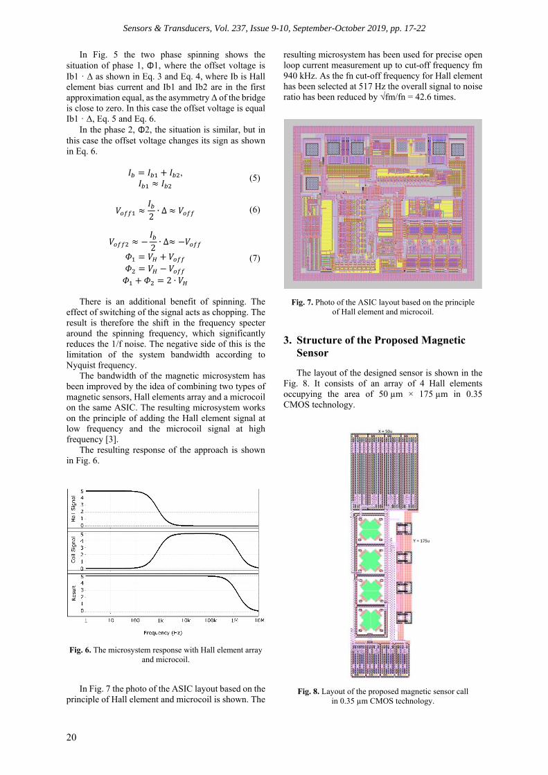
Sensors & Transducers, Vol. 237, Issue 9-10, September-October 2019, pp. 17-22
20
In Fig. 5 the two phase spinning shows the situation of phase 1, Φ1, where the offset voltage is Ib1 · Δ as shown in Eq. 3 and Eq. 4, where Ib is Hall element bias current and Ib1 and Ib2 are in the first approximation equal, as the asymmetry Δ of the bridge is close to zero. In this case the offset voltage is equal Ib1 · Δ, Eq. 5 and Eq. 6.
In the phase 2, Φ2, the situation is similar, but in this case the offset voltage changes its sign as shown in Eq. 6.
,
(5)
2 ∙ ∆ (6)
2 ∙ ∆
2 ∙
(7)
There is an additional benefit of spinning. The
effect of switching of the signal acts as chopping. The result is therefore the shift in the frequency specter around the spinning frequency, which significantly reduces the 1/f noise. The negative side of this is the limitation of the system bandwidth according to Nyquist frequency.
The bandwidth of the magnetic microsystem has been improved by the idea of combining two types of magnetic sensors, Hall elements array and a microcoil on the same ASIC. The resulting microsystem works on the principle of adding the Hall element signal at low frequency and the microcoil signal at high frequency [3].
The resulting response of the approach is shown in Fig. 6.
Fig. 6. The microsystem response with Hall element array and microcoil.
In Fig. 7 the photo of the ASIC layout based on the principle of Hall element and microcoil is shown. The
resulting microsystem has been used for precise open loop current measurement up to cut-off frequency fm 940 kHz. As the fn cut-off frequency for Hall element has been selected at 517 Hz the overall signal to noise ratio has been reduced by √fm/fn = 42.6 times.
Fig. 7. Photo of the ASIC layout based on the principle of Hall element and microcoil.
3. Structure of the Proposed Magnetic Sensor
The layout of the designed sensor is shown in the Fig. 8. It consists of an array of 4 Hall elements occupying the area of 50 µm × 175 µm in 0.35 CMOS technology.
Fig. 8. Layout of the proposed magnetic sensor call in 0.35 µm CMOS technology.
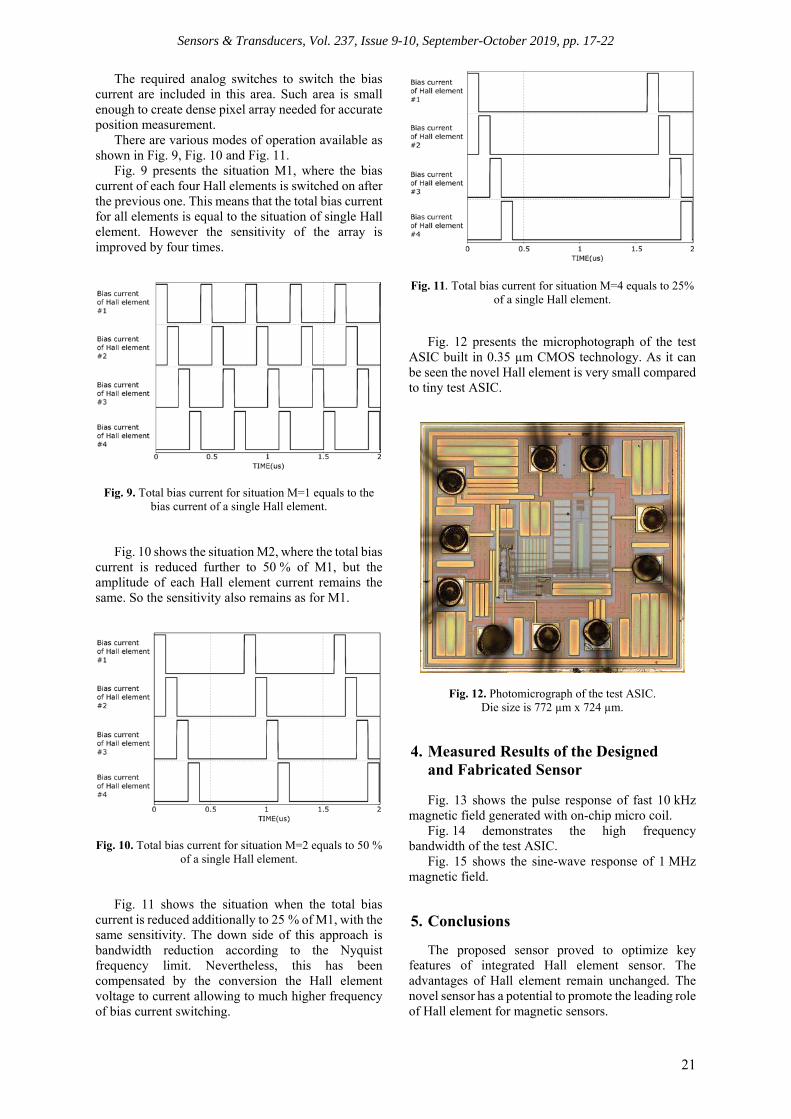
Sensors & Transducers, Vol. 237, Issue 9-10, September-October 2019, pp. 17-22
21
The required analog switches to switch the bias current are included in this area. Such area is small enough to create dense pixel array needed for accurate position measurement.
There are various modes of operation available as shown in Fig. 9, Fig. 10 and Fig. 11.
Fig. 9 presents the situation M1, where the bias current of each four Hall elements is switched on after the previous one. This means that the total bias current for all elements is equal to the situation of single Hall element. However the sensitivity of the array is improved by four times.
Fig. 9. Total bias current for situation M=1 equals to the bias current of a single Hall element.
Fig. 10 shows the situation M2, where the total bias current is reduced further to 50 % of M1, but the amplitude of each Hall element current remains the same. So the sensitivity also remains as for M1.
Fig. 10. Total bias current for situation M=2 equals to 50 % of a single Hall element.
Fig. 11 shows the situation when the total bias current is reduced additionally to 25 % of M1, with the same sensitivity. The down side of this approach is bandwidth reduction according to the Nyquist frequency limit. Nevertheless, this has been compensated by the conversion the Hall element voltage to current allowing to much higher frequency of bias current switching.
Fig. 11. Total bias current for situation M=4 equals to 25% of a single Hall element.
Fig. 12 presents the microphotograph of the test ASIC built in 0.35 µm CMOS technology. As it can be seen the novel Hall element is very small compared to tiny test ASIC.
Fig. 12. Photomicrograph of the test ASIC. Die size is 772 µm x 724 µm.
4. Measured Results of the Designed and Fabricated Sensor Fig. 13 shows the pulse response of fast 10 kHz
magnetic field generated with on-chip micro coil. Fig. 14 demonstrates the high frequency
bandwidth of the test ASIC. Fig. 15 shows the sine-wave response of 1 MHz
magnetic field.
5. Conclusions
The proposed sensor proved to optimize key features of integrated Hall element sensor. The advantages of Hall element remain unchanged. The novel sensor has a potential to promote the leading role of Hall element for magnetic sensors.
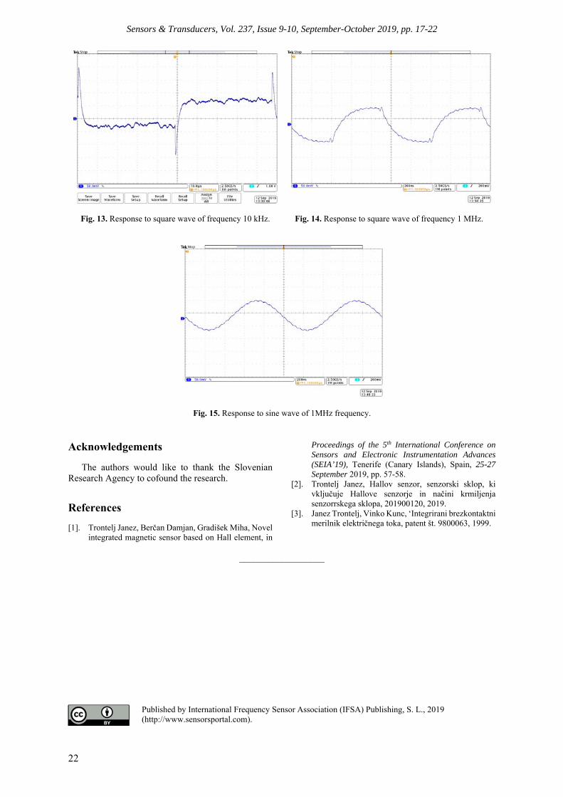
Sensors & Transducers, Vol. 237, Issue 9-10, September-October 2019, pp. 17-22
22
Fig. 13. Response to square wave of frequency 10 kHz.
Fig. 14. Response to square wave of frequency 1 MHz.
Fig. 15. Response to sine wave of 1MHz frequency.
Acknowledgements
The authors would like to thank the Slovenian Research Agency to cofound the research.
References [1]. Trontelj Janez, Berčan Damjan, Gradišek Miha, Novel
integrated magnetic sensor based on Hall element, in
Proceedings of the 5th International Conference on Sensors and Electronic Instrumentation Advances (SEIA’19), Tenerife (Canary Islands), Spain, 25-27 September 2019, pp. 57-58.
[2]. Trontelj Janez, Hallov senzor, senzorski sklop, ki vključuje Hallove senzorje in načini krmiljenja senzorrskega sklopa, 201900120, 2019.
[3]. Janez Trontelj, Vinko Kunc, ‘Integrirani brezkontaktni merilnik električnega toka, patent št. 9800063, 1999.
__________________
Published by International Frequency Sensor Association (IFSA) Publishing, S. L., 2019 (http://www.sensorsportal.com).

Sensors & Transducers, Vol. 237, Issue 9-10, September-October 2019, pp. 23-29
23
Sensors & Transducers
Published by IFSA Publishing, S. L., 2019 http://www.sensorsportal.com
Accurate Level Measurement Based on Capacitive Differential Pressure Sensing
* Parisa ESMAILI, Federico CAVEDO and Michele NORGIA
Politecnico di Milano, via Ponzio, 20133, Milan, Italy Tel.: +39-02-2399.3601, fax: 3412 E-mail: [email protected]
Received: 30 August 2019 /Accepted: 27 September 2019 /Published: 30 November 2019 Abstract: In this paper, a capacitive differential pressure sensor is characterized as a liquid level measurement system. The sensor is configured as a first-order low pass filter. Different operating frequencies have been defined and a DFT based feedback loop is proposed in addition to eliminate the impact of interferences at predefined operating frequency. The phase-sensitive demodulation of the signal is performed using a single-tone DFT algorithm, acquiring both excitation and output signals. Each signal is acquired at 10 MSPS and the DFT is computed on 8000 samples. The sensitivity of the proposed instrument is 40ppm/mm with very good linearity and error as low as ±0.3 mm. The measurement characterization of the sensor indicates good performances as low-cost level measurement system. Keywords: Liquid level measurement, Differential capacitive pressure, Phase sensitive detection, Digital Lock-in amplifier, Single-tone DFT. 1. Introduction
In a wide range of scientific and industrial
applications, precise liquid level measurement plays a crucial role. To achieve accurate level detection, request for dedicated techniques that are working to tighter accuracy limits become more severe while production costs are limited due to economic issues.
As a result, the requirement for designing an instrument, to be both accurate and cost-effective, becomes ever harder to satisfy. Various techniques have been proposed in this manner. These approaches can be categorized into either direct/indirect or contact/non-contact methods. Typically, direct methods such as floating based level measurement systems are limited by the lack of precision and accuracy. Several approaches in the field of contact-based indirect level measurement such as time domain reflectometry (TDR), capacitive and pressure-based
reading systems have been proposed. These approaches eliminate the requirement of moving part as in conventional techniques. However, the capacitive probes suffer from miss-reading not only due to parasitic capacitance but also to fluctuations [1-2]. Although TDR based approaches are very accurate solutions, but pulse-duration measurements with high resolution requires high costs for the overall data-acquisition system. In addition to contact-based methods, different non-contact indirect methods such as ultrasonic [3-4], vision [5], optical [6-8], microwave [9-12] have been proposed to measure the level. In techniques based on Time of Flight (TOF) principle, the performance becomes poor when they are subjected to measure the quantity of liquid with low dielectric constant due to weak back reflection. In addition, the presence of the foam on the surface of the liquid results into inaccurate level detection during acceleration. In [13], a low-cost and indirect contact-
http://www.sensorsportal.com/HTML/DIGEST/P_3106.htm

Sensors & Transducers, Vol. 237, Issue 9-10, September-October 2019, pp. 23-29
24
based level detection instrument is proposed based on differential pressure sensing approach.
A Capacitive differential pressure sensor is used as a sensing element in the configuration of first-order low pass filter where a sinusoidal signal generated by Digital-to-Analog Converter (DAC) of multi-function instrument to drive it. In order to eliminate any non-linearity, induced by distortion of the driving signal, the output signal of the proposed instrument is expressed as the ratio between the signal at the output of the operational amplifier and input signal. Then, single-bin DFT (Discrete Fourier Transform) is performed based on evaluating the phase and quadrature component with a digital synchronous receiver, which performs the multiplication of the sampled signal for two quadrature signals to then evaluate the Fourier coefficients. The performance of the proposed instrument has been evaluated experimentally under steady state condition. However, presence of the interferences at selected operating frequency affects the performance. To avoid this, a DFT based feedback loop is proposed here in evaluating operating frequency and detect the level accurately in addition.
2. Liquid Level Measurement Based on Differential Pressure Sensing Principle Pressure based level sensing technique has been
proposed for the analysis and monitoring of a ship’s stability [14]. The Pressure transmitter measures level based on the principle that pressure (P) is proportional to the level of the liquid multiplied by its specific gravity given by (1).
, (1)
where and g are the density and gravitational acceleration respectively. Depending on the technology, different types of pressure transducers are commercially available such as piezoresistive, piezoelectric and capacitive pressure transducers. Fig. 1 represents the working principle of the capacitive differential pressure sensor for measuring liquid level, used in the proposed level instrument. The output of the transducer is an equivalent capacitance which changes its value as a function of the applied pressure. In the frequency-shift-based implementation, the capacitive sensor is used in an RC low pass filter, such that a change in capacitance causes a change in frequency response. The transfer function of a low pass filter is represented in (2) as a function of frequency where is its cut-off frequency. While working at cut-off frequency provides maximum sensitivity in the phase, working close to this frequency maximum sensitivity in gain and linearity can be achieved. This is where the excitation signal is generated to derive transducer and measure accurately the level of the liquid.
Fig. 1. Capacitance variation in capacitive differential pressure transducer due to applied pressure.
11
(2)
Due to different frequency dependency of various
noise sources, as in many electrical and physical systems, there is increasing in noise level as the frequency approaches DC. In case of having flexibility in the choice of the modulation frequency, part of the spectrum can be chosen as the operating zone where the noise level is the lowest. Working at higher frequencies requires a narrowband filter to recover the signal. Alternatively, phase sensitive detection technique is introduced to move the modulated signal back to dc while filtering out other signals that are not synchronized to the reference signal [15]. Here, the single-bin DFT is performed based on evaluating the phase and quadrature component with a digital synchronous receiver, which performs the multiplication of the sampled signal for two quadrature signals (sine and cosine at the same frequency), to then evaluate the Fourier coefficients. From the two-phase and quadrature signals, amplitude and phase measurements are easily obtained. The amplitude and phase measurements become the more accurate depending on how many points have been acquired. This is due to the contribution of white noise on every single bin which affects the measurement accuracy in case of dealing with low SNR (Signal to Noise Ratio).
In Vandermonde matrix (3), introduced by Sylvester [16] in 1867, DFT is expressed as the DFT matrix assuming the unitary definition of the DFT.
F=
. . ⋯ .. . … .⋮ ⋮ ⋱ ⋮. . ⋯ . , (3)
where . As shown in (4), the DFT becomes a unitary transformation, defined by a unitary
matrix with unitary normalization √ constants.
1√ (4)

Sensors & Transducers, Vol. 237, Issue 9-10, September-October 2019, pp. 23-29
25
Parseval's theorem for DFT is represented by (5). According to this, the sum (or integral) of the square of a function is equal to the sum of the square of its transform [17].
| | | | (5)
Let’s assume that x[n] represents a zero-mean
white noise process with variance σ . Applying the expectation of both sides results into (6) and (7).
∑ | | ∑ | | , (6) | | (7) Finally, by simplifying N, it is concluded that
expected value of the noise spectrum's squared magnitude does not change by increasing DFT length under unitary definition of DFT.
| | (8) Now consider x[n] is a sinusoidal tone of interest.
For simplicity, assume x[n]=1 (considering tone of the interest is at zero frequency). Recalling (4):
√ ∑ , (9)
√ ∑ , (10)
√ , (11)
| | (12) Nevertheless, the expected squared magnitude of
the noise process in the frequency domain stays constant, the expected frequency-domain squared magnitude for a narrowband signal is proportional to N. This could be evaluated from filter point of view since The DFT implements a uniformly spaced bank N of critically sampled filters. The frequency response of each filter the shape of a Dirichlet kernel, whose width is inversely proportional to N. Therefore, the frequency-domain SNR can be effectively increased the by increasing the DFT length N. Increase the observation duration or in the other words performing longer DFT implies that each bandpass filter covers a smaller portion of the frequency band resulting less noise power passed by each bin's corresponding filter.
3. Measuring Circuit In this paper, the instrument design is divided into
three main parts: the capacitive differential pressure transducer, the analog frontend for signal condition and a digital part to provide sensor operating condition and making the elaboration as represented in Fig. 2.
The Excitation signal is generated by DAC. Using two ADCs working in parallel and triggered by the same clock signal, it is possible to acquire the DAC output used to drive the transducer and the output of analog frontend at the same time. In this case any non-linearity induced by distortion of the driving signal is eliminated. Then, Digital Signal Processing unit (DSP) processes the acquired signals using DFT and provides respective phase and quadrature.
Fig. 2. Block diagram of the proposed instrument including capacitive differential pressure senor, one DAC
and two ADCs.
Fig. 3 shows the output defined as ratio between the output of operational amplifier and the excitation signal as function of frequency. As shown in this figure, linearity is guaranteed at lower than 200 kHz and higher than 400 kHz. Therefore, Optimum operating frequency can be selected based on sensitivity curve where it is defined in [ppm/Hz] unit, as shown in Fig. 4.
Fig. 3. Frequency response of DP based level sensor.
Following the Fig. 4, working at almost 68 kHz provides maximum sensitivity. The zoomed part of graph shows about 10 % reduction in sensitivity in

Sensors & Transducers, Vol. 237, Issue 9-10, September-October 2019, pp. 23-29
26
case of working at 100 kHz and it is acceptable in case of considering uncertainty while determining equivalent capacitance of DP at zero pressure (offset).
Fig. 4. Sensitivity defined in [ppm/Hz] V.S operating frequency.
It should be noted that working close to the pole frequency should be guaranteed in case of considering different operating frequencies. Therefore, A digital potentiometer can be used to adjust the pole frequency which has the same function as a normal potentiometer but instead of mechanical action it uses digital signals and switches.
4. Feedback Loop on Operating Frequency Selection As mentioned earlier, part of the spectrum where
the noise level is lowest can be selected if there is some freedom in the choice of modulation frequency. However, presence of unwanted and strong interference very close to selected operated frequency affects strongly the performance. One solution to discard the interference is to reduce main lobe width by increasing length of DFT. However, there is always tradeoff between time and frequency resolution. In addition, this solution is limited by hardware implementation and high cost. Alternatively, a feed-back loop can be applied based on spectrum analysis to decide whether the operating frequency should be updated. Fig. 5 shows flowchart of the feed-back loop where 10 and 100 kHz have been considered as default operating frequencies.
As shown in this figure, first step is to stop the excitation signal to evaluate suitable operating frequency. After choosing the right pole frequency and changing filter configuration, DFT is performed. In this case, detected amplitude of the specified DFT bin shows the contribution of the noise on that bin since there is no excitation signal. It is expected to detect the amplitude of two tones in same range in case of interference free condition. However, higher detected amplitude at each predefined frequency results into
discarding associated frequency due to presence of interference.
Fig. 5. Flowchart of DFT based feedback loop.
5. Experimental Setup
The prototype of proposed level instrument and experimental setup with the liquid tank have is illustrated in Fig. 6. Graduated cylinder test tank is mounted on high pressure while low pressure side is open to the air.
Fig. 6. Prototype of the proposed level instrument.

Sensors & Transducers, Vol. 237, Issue 9-10, September-October 2019, pp. 23-29
27
The Pressure sensing element is a differential capacitive pressure sensor in range of 0~7.5 kPa which is connect to the input operational amplifier in the configuration of first order low pass filter. A multi-function instrument (DIGILENT-Analog Discovery 2) is used to generate excitation sinusoidal signal at different frequencies with amplitude of 2 provided by function generator (±5 V, 14-bit, 100 MS/s). Using Dual channel 14-bit, ADC form Analog Discovery 2, the excitation and output of the operational amplifier are acquired simultaneously. Both signals are processed using DFT and provides respective real and imaginary values. Each signal is acquired at 10 MSPS and the DFT is computed on 8000 samples. Fig. 7 demonstrates measuring circuit with digital signal generator and two synchronous samplers. Further steps to perform DFT algorithm and amplitude detection is done in LabVIEW from National Instrument.
Fig. 7. Measuring circuit block diagram of the proposed instrument with signal generation, acquisition
and processing block diagram.
Recalling the feedback loop, the detected amplitude in absence of excitation signal determines the presence of interference in selected frequency. After updating the value for resistor and performing DFT at 10 and 100 kHz, different amplitudes are detected at predefined frequencies. As shown in Fig. 8, the presence of a strong interference at 10 kHz is more evident due to its high amplitude. While working at 100 kHz is more convenient. Here, the frequency sweep is repeated every 10 ms.
To determine sensitivity curve, the water level in a test tank was increased in steps by adding water. Fig. 9 shows the sensitivity curve of the proposed instrument. As shown in this figure, the sensitivity is 40 ppm/mm.
To evaluate repeatability error, additional experiments have been performed. Fig. 10 shows the measured level increment and decrement using proposed instrument for repeated measurements to evaluated repeatability error of the instrument. Corresponding error is illustrated in Fig. 11. As result
shows, the repeatability error for the proposed instrument is about ±0.3 mm.
Fig. 8. Magnitude (in dB) of DFT spectrum of 8000 sample of without excitation signal at 10 kHz and 100 kHz.
Fig. 9. Sensitivity curve of the proposed instrument defined as [ppm/mm].
Fig. 10. Measured relative value of the level V.S reference values during repeatability test.

Sensors & Transducers, Vol. 237, Issue 9-10, September-October 2019, pp. 23-29
28
Fig. 11. Absolute values for repeatability error of the proposed instrument.
7. Conclusions
As low-cost level measurement system, a digital lock in amplifier based liquid level instrument is proposed in this paper, using differential pressure sensing approach. Different operating frequencies have been defined and a DFT based feedback loop is proposed in addition to eliminate the impact of interferences at predefined operating frequency. The output signal of the proposed instrument is defined as the ratio between the signal at the output of the operational amplifier and input signal to eliminate any non-linearity, induced by distortion of the driving signal. Dual channel ADC form DIGILENT is used to acquire the excitation and output of the operational amplifier simultaneously. Both signals are processed using DFT and provide respective real and imaginary values. Each signal is acquired at 10 MSPS and the DFT is computed on 8000 samples. The sensitivity of the proposed instrument reported here is 40 ppm/mm, with good linearity. In addition, the repeatability test is performed, and the error is determined as ±0.3 mm.
Acknowledgements
The authors would like to thank Fondazione Ing. Paolo Foresio for the financial support of the research activity. References [1]. H. Canbolat, A Novel Level Measurement Technique
Using Three Capacitive Sensors for Liquids, IEEE Transactions on Instrumentation and Measurement, Vol. 58, Issue 10, 2009, pp. 3762-3768.
[2]. S. Bera, H. Mandal, S. Saha, A. Dutta, Study of a Modified Capacitance-Type Level Transducer for Any Type of Liquid, IEEE Transactions on Instrumentation and Measurement, Vol. 63, Issue 3, 2014, pp. 641-649.
[3]. D. Zou, M. Yang, X. Zhan, R. He, X. Li, Assessment of air entrainment in stirred tanks using capacitive sensors, Sensors and Actuators A: Physical, Vol. 216, 2014, pp. 92-101.
[4]. J. Terzic, C. Nagarajah, M. Alamgir, Fluid level measurement in dynamic environments using a single ultrasonic sensor and Support Vector Machine (SVM), Sensors and Actuators A: Physical, Vol. 161, Issue 1-2, 2010, pp. 278-287.
[5]. Peng Li, Yulei Cai, Xiaolong Shen, S. Nabuzaale, Jie Yin, Jiaqiang Li, An Accurate Detection for Dynamic Liquid Level Based on MIMO Ultrasonic Transducer Array, I EEE Transactions on Instrumentation and Measurement, Vol. 64, Issue 3, 2015, pp. 582-595.
[6]. L. Nguyen, B. Schaeli, D. Sage, S. Kayal, D. Jeanbourquin, D. Barry, L. Rossi, Vision-based system for the control and measurement of wastewater flow rate in sewer systems, Water Science & Technology, Vol. 60, Issue 9, 2009, pp. 2281-2289.
[7]. K. Sohn, J. Shim, Liquid-level monitoring sensor systems using fiber Bragg grating embedded in cantilever, Sensors and Actuators A: Physical, Vol. 152, Issue 2, 2009, pp. 248-251.
[8]. W. Wang, F. Li, Large-range liquid level sensor based on an optical fiber extrinsic Fabry–Perot interferometer, Optics and Lasers in Engineering, Vol. 52, Issue 1, 2014, pp. 201-205.
[9]. D. Melchionni, M. Norgia, Optical system for liquid level measurements, Review of Scientific Instruments, Vol. 85, Issue 7, 2014, p. 075113.
[10]. A. Cataldo, L. Tarricone, F. Attivissimo, A. Trotta, Simultaneous measurement of dielectric properties and levels of liquids using a TDR method, Measurement, Vol. 41, Issue 3, 2008, pp. 307-319.
[11]. A. Cataldo, E. Piuzzi, E. De Benedetto, G. Cannazza, Experimental Characterization and Performance Evaluation of Flexible Two-Wire Probes for TDR Monitoring of Liquid Level, IEEE Transactions on Instrumentation and Measurement, Vol. 63, Issue 12, 2014, pp. 2779-2788.
[12]. L. Bengtsson, New design ideas for TDR-based liquid level detectors, in Proceedings of the Instrumentation and Measurement Technology Conference (I2MTC 2017), Turin, Italy, 22-25 May 2017, pp. 1-6.
[13]. P. Esmaili, F. Cavedo, M. Norgia, Differential pressure sensing based on phase sensitive detection for liquid level measurement, in Proceedings of the 5th International Conference on Sensors Engineering and Electronics Instrumentation Advances (SEIA'2019), Tenerife (Canary Islands), Spain, 25-27 September 2019, pp. 139-142.
[14]. Huayao Zheng, Yunqian Huang, Yinzhong Ye, New level sensor system for ship stability analysis and monitor, IEEE Transactions on Instrumentation and Measurement, Vol. 48, Issue 6, 1999, pp. 1014-1017.
[15]. M. L. Meade, Lock-in Amplifiers: Principles and Applications, Peter Peregrinus Ltd, London, UK, 1983.
[16]. Sylvester J. J., Thoughts on inverse orthogonal matrices, simultaneous sign successions, and tessellated pavements in two or more colors, with applications to Newton’s rule, ornamental tile-work, and the theory of numbers, The London, Edinburgh, and Dublin Philosophical Magazine and Journal of Science, Vol. 34, Issue 232, 1867, pp. 461-475.
[17]. Kaplan W, Advanced Calculus, 4th ed., Addison-Wesley, 1992.

Sensors & Transducers, Vol. 237, Issue 9-10, September-October 2019, pp. 23-29
29
__________________
Published by International Frequency Sensor Association (IFSA) Publishing, S. L., 2019 (http://www.sensorsportal.com).
Sensors & Transducers, Vol. 237, Issue 9-10, September-October 2019, pp. 30-36
30
Sensors & Transducers
Published by IFSA Publishing, S. L., 2019 http://www.sensorsportal.com
Piezoelectric Ceramic Transducers as Time-Varying Displacement Sensors in Nanopositioners
3 Massoud HEMMASIAN ETTEFAGH, 2 Mokrane BOUDAUD,
1, 2, * Ali BAZAEI, 1 Zhiyong CHEN and 2 Stéphane RÉGNIER 1 University of Newcastle, School of Electrical Engineering and Computing,
Callaghan, NSW 2308, Australia 2 Sorbonne University, Institute for Intelligent Systems and Robotics (ISIR), Paris, France
3 Huazhong University of Science and Technology, School of Artificial Intelligence and Automation, Wuhan, China
1 Tel.: +61 240238982, fax: +61 249216993 E-mail: [email protected]
Received: 30 August 2019 /Accepted: 27 September 2019 /Published: 30 November 2019 Abstract: We present a direct measurement of stage displacement in piezo-driven nanopositioners via piezoelectric (PZT) ceramics. In addition to compactness and affordability, our study shows that within the sensing bandwidth, the sensor is able to track time-varying large signal profiles of stage displacement accurately without utilizing signal conditioning devices. Also, the sensor can be used to capture cross coupling effect in orthogonal axes of motion. For the full-scale range, accuracy of the suggested sensor is less than 27 nm in the sensing bandwidths when the sensor is calibrated with a constant scaling factor. The 3σ-resolution of the sensor is 1.9 nm. Keywords: Displacement sensor, Piezoelectric sensor, Nanopositioning stage, Time-varying displacement, Scanning. 1. Introduction
The accurate measurement of high frequency
movement is essential for many micro and nano positioning systems including scanners in selective laser sintering applications [15-17], microscanner mirrors [12-14], and nanopostioners for scanning probe microscopy [1-11].
PZT sensors have many desired characteristics such as high bandwidth, small foot print, small noise level, compactness, and affordability [18]. The electromechanical coupling between electrical field and stress makes piezoelectric ceramics an ideal choice for strain, force, pressure, acceleration, and temperature measurement, and for energy harvesting
[19-20]. Nevertheless, no study has been reported on piezoelectric ceramics to address the direct measurement of stage displacement in nanoposi-tioning systems, primarily because the sensor response exhibits drift and decreasing sensitivity at low frequencies from its RC high-pass characteristic. In scanning tasks, however, the high-pass decrease issue would not pose a problem since the displacement oscillates rapidly. In order to measure the displacement of nanopositioning stage directly, our study addresses the large signal characterization of piezoelectric ceramic response in a custom-made high-bandwidth Nanopositioner.
Few works employed piezoelectric ceramics as sensors in nanopositioners. In order to damp the dynamical vibration of a nanopositioners, the authors
http://www.sensorsportal.com/HTML/DIGEST/P_3107.htm
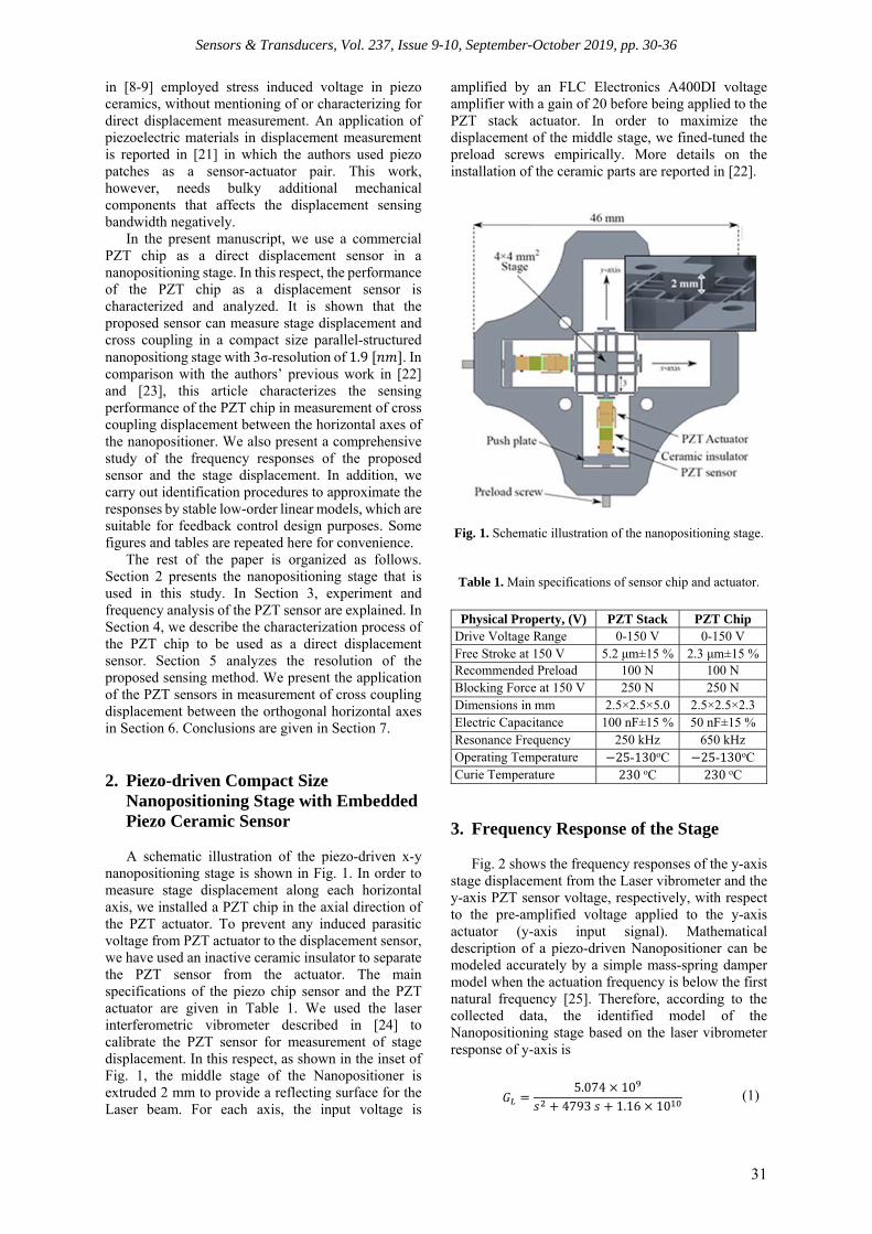
Sensors & Transducers, Vol. 237, Issue 9-10, September-October 2019, pp. 30-36
31
in [8-9] employed stress induced voltage in piezo ceramics, without mentioning of or characterizing for direct displacement measurement. An application of piezoelectric materials in displacement measurement is reported in [21] in which the authors used piezo patches as a sensor-actuator pair. This work, however, needs bulky additional mechanical components that affects the displacement sensing bandwidth negatively.
In the present manuscript, we use a commercial PZT chip as a direct displacement sensor in a nanopositioning stage. In this respect, the performance of the PZT chip as a displacement sensor is characterized and analyzed. It is shown that the proposed sensor can measure stage displacement and cross coupling in a compact size parallel-structured nanopositiong stage with 3σ-resolution of 1.9[ ]. In comparison with the authors’ previous work in [22] and [23], this article characterizes the sensing performance of the PZT chip in measurement of cross coupling displacement between the horizontal axes of the nanopositioner. We also present a comprehensive study of the frequency responses of the proposed sensor and the stage displacement. In addition, we carry out identification procedures to approximate the responses by stable low-order linear models, which are suitable for feedback control design purposes. Some figures and tables are repeated here for convenience.
The rest of the paper is organized as follows. Section 2 presents the nanopositioning stage that is used in this study. In Section 3, experiment and frequency analysis of the PZT sensor are explained. In Section 4, we describe the characterization process of the PZT chip to be used as a direct displacement sensor. Section 5 analyzes the resolution of the proposed sensing method. We present the application of the PZT sensors in measurement of cross coupling displacement between the orthogonal horizontal axes in Section 6. Conclusions are given in Section 7. 2. Piezo-driven Compact Size
Nanopositioning Stage with Embedded Piezo Ceramic Sensor A schematic illustration of the piezo-driven x-y
nanopositioning stage is shown in Fig. 1. In order to measure stage displacement along each horizontal axis, we installed a PZT chip in the axial direction of the PZT actuator. To prevent any induced parasitic voltage from PZT actuator to the displacement sensor, we have used an inactive ceramic insulator to separate the PZT sensor from the actuator. The main specifications of the piezo chip sensor and the PZT actuator are given in Table 1. We used the laser interferometric vibrometer described in [24] to calibrate the PZT sensor for measurement of stage displacement. In this respect, as shown in the inset of Fig. 1, the middle stage of the Nanopositioner is extruded 2 mm to provide a reflecting surface for the Laser beam. For each axis, the input voltage is
amplified by an FLC Electronics A400DI voltage amplifier with a gain of 20 before being applied to the PZT stack actuator. In order to maximize the displacement of the middle stage, we fined-tuned the preload screws empirically. More details on the installation of the ceramic parts are reported in [22].
Fig. 1. Schematic illustration of the nanopositioning stage.
Table 1. Main specifications of sensor chip and actuator.
Physical Property, (V) PZT Stack PZT Chip
Drive Voltage Range 0-150 V 0-150 V Free Stroke at 150 V 5.2 μm±15 % 2.3 μm±15 % Recommended Preload 100 N 100 N Blocking Force at 150 V 250 N 250 N Dimensions in mm 2.5×2.5×5.0 2.5×2.5×2.3 Electric Capacitance 100 nF±15 % 50 nF±15 % Resonance Frequency 250 kHz 650 kHz Operating Temperature −25-130oC −25-130oC Curie Temperature 230oC 230 oC
3. Frequency Response of the Stage
Fig. 2 shows the frequency responses of the y-axis stage displacement from the Laser vibrometer and the y-axis PZT sensor voltage, respectively, with respect to the pre-amplified voltage applied to the y-axis actuator (y-axis input signal). Mathematical description of a piezo-driven Nanopositioner can be modeled accurately by a simple mass-spring damper model when the actuation frequency is below the first natural frequency [25]. Therefore, according to the collected data, the identified model of the Nanopositioning stage based on the laser vibrometer response of y-axis is
= 5.074 × 10+ 4793 + 1.16 × 10 (1)

Sensors & Transducers, Vol. 237, Issue 9-10, September-October 2019, pp. 30-36
32
According to Fig. 2 and Eq. (1), the stage has a dominant resonance mode at 17.1[kHz], its 3-dB bandwidth is 9.4[kHz], and the damping ratio is = 0.022.
Fig. 2. Frequency response of y-axis.
Similarly, the identified model from the collected frequency response data of the PZT sensor voltage is
= 1.6( + 0.4)( + 3090 + 4.13 × 10 )( + 167)( + 5706 + 1.22 × 10 ) (2)
As Fig. 2 shows, the frequency response of the
PZT sensor voltage exhibits a low 3-dB corner frequency at 32[ ], as well as a high 3-dB corner frequency at 6[ ].
According to Fig. 2, the frequency response of the PZT sensor exhibits a sharp notch at 10.2[ ] that does not appear in the laser vibrometer response. As Eq. (2) demonstrates, this notch is quantified by a pair of lightly damped complex zeros with = 6.43 × 10 , = 0.024, and imposes an
upper limit on the bandwidth of the PZT sensor. These complex zeros are the result of the natural frequency of the unloaded Nanopositioner at the same frequency. In Fig. 3, the first mode shape and natural frequency of the unloaded structure is obtained via finite element methods. The value of the natural frequency is 10.8[ ] which is very close to the frequency location of the lightly damped complex zeros. As the stage requires negligible external force to vibrate at its unloaded natural frequency, the interaction force between the PZT actuator and the rest of the system is significantly reduced at this frequency. As the PZT sensor responses to the interaction force and since negligible amount of force is transmitted at this frequency, a dominant pair of imaginary zeros are exhibited only in the PZT sensor response but not in the directly measured stage position (by the Laser). As shown in [8], a mass-spring model can also demonstrate the existence of such zero in the interaction force between the PZT actuator and PZT sensor.
Because of the dominant imaginary zero at 10.5[ ], the high-3dB corner frequency of the PZT sensor is around 6400[ ]. Fig. 2 shows that at low frequencies the magnitude response of the PZT sensor reduces by 20 dB per decade as the actuation frequency decreases toward zero. This reduction is accompanied with a phase lead of almost 90 degrees, which indicates the existence of a single zero at the origin. This behavior is in consistency with the response of a resistive load driven by series combination of a voltage source and a capacitor acting as a first-order high-pass filter.
Fig. 3. A finite element modal analysis of the unloaded Nanopositioner predicts the first natural frequency at 10.88[ ]. The magnified mode shape of the monolithic structure at this frequency indicates the
deformation along y-axis [22].
The 3-dB corner frequency of such high-pass filter is 12 [ ], (3)
where and denote the total resistance and capacitance of the filter, respectively. During the frequency response experiment, the PZT sensor is connected to the measurement instruments with the total resistance of = 88[ Ω]. Also, as we measured after preloading, the capacitance of the PZT sensor is around = 60[ ]. Therefore, employing (1), the 3-dB corner frequency of the high-pass filter is 30.14[ ], which is in close agreement with the measured low corner frequency of 32[ ] in Fig. 2. Note that further reduction in the low corner frequency is achievable by connecting the PZT sensor to an instrumentation with a higher resistance. Finally, using the low and high 3-dB corners, the sensor can directly measure the stage displacement in the frequency range of (32-6400)[ ].
-40
-20
0
20
40Laser sensor for stage displacementIdentified model from Laser sensorPZT chip sensor voltageIdentified model from PZT sensor
100 101 102 103 104-270
-180
-90
0
90
180
Bode Diagram
Frequency (Hz)
Low corner Frequency
High corner Frequency

Sensors & Transducers, Vol. 237, Issue 9-10, September-October 2019, pp. 30-36
33
4. Characterization of the PZT Sensor The calibration process of the PZT sensor on the y-
axis is carried out by applying a 500[ ] sinusoidal voltage with the range of 0-140[ ], whose frequency is well between the low and the high 3-dB corner frequencies in Fig. 2. The signals from the Laser, the PZT sensor, and the input voltage to the amplifier are simultaneously collected and displayed in Fig. 4(a). In the figure, the voltage value of the PZT sensor and input signal are linearly scaled to have the same extrema as the read out of the laser sensor. Using this experiment, the sensitivity of the PZT sensor is
characterized as 1377 . This sensitivity is obtai-
ned from the experimentally obtained scale factor as: Senisitivity= 1scalefactor = 1726[ ] (4)
The error value, presented in Fig. 4(b), shows an
increase in the amplitude of its vibration around time 1.4[ ], which is the time when the input signal reaches to its peak value. The inset of Fig. 4(a) shows the close-up view of the signals around this point, where the input signal exhibits a sharp change at peak value. This sharp change is because of the non-smooth profile of sinewave generator, and provokes high frequency vibrations that are close to the resonance mode of the structure. Another similar vibration is also excited when the input reaches its minimum around 0.4[ ]. Further examination of the error value indicates that the frequency of the vibration is around 17[ ], which is the fundamental frequency obtained from the frequency response of Fig. 2.
Fig. 5 shows the hysteresis curves obtained by the laser and PZT sensors for the 500[ ] sinusoidal actuation voltage with the range of 0-140[ ]. It shows that the large hysteretic deviation of the displacement profile, measured by the laser sensor, is precisely captured by the PZT sensor.
In order to validate the scaling factor in Eq. (4), we carry out a similar test for the PZT sensor at a different frequency, whilst the scaling factor is 726[ ]. As we
can see in Fig. 6, the measurement error at this new frequency is very similar to the measurement error of the 500[ ]sinusoidal test, indicating high performance of the PZT chip for displacement measurement within the sensing bandwidth (32-6400)[ ].
In order to determine accuracy of the PZT sensor, further examination with large amplitude sinusoidal excitation at other frequencies within the sensing bandwidth (32-6400)[ ] are performed. Fig. 7 and Table 2 report the deviation range and average absolute error of the PZT sensor, respectively. Note that the minor excitation of the resonant mode of the open-loop Nanopositioner at 17[ ] due to the non-smooth profile of the input at the peak and the minimum points plays the main role in the error value. As this frequency is far beyond the high-corner
frequency, which is 6.4[ ], the actual error within the sensing bandwidth is expected to be much smaller.
Fig. 4. Calibration test by 500[ ] sinusoidal excitation [22].
Fig. 5. Hysteresis curves from Laser and PZT sensors [22].
Fig. 6. Validation test at 1583[ ] sinusoidal excitation [22].
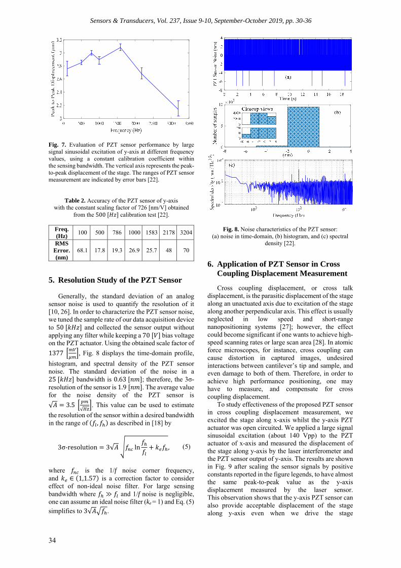
Sensors & Transducers, Vol. 237, Issue 9-10, September-October 2019, pp. 30-36
34
Fig. 7. Evaluation of PZT sensor performance by large signal sinusoidal excitation of y-axis at different frequency values, using a constant calibration coefficient within the sensing bandwidth. The vertical axis represents the peak-to-peak displacement of the stage. The ranges of PZT sensor measurement are indicated by error bars [22].
Table 2. Accuracy of the PZT sensor of y-axis with the constant scaling factor of 726 [nm/V] obtained
from the 500[ ] calibration test [22].
Freq. (Hz) 100 500 786 1000 1583 2178 3204
RMS Error. (nm)
68.1 17.8 19.3 26.9 25.7 48 70
5. Resolution Study of the PZT Sensor Generally, the standard deviation of an analog
sensor noise is used to quantify the resolution of it [10, 26]. In order to characterize the PZT sensor noise, we tuned the sample rate of our data acquisition device to 50[ ] and collected the sensor output without applying any filter while keeping a 70[ ] bias voltage on the PZT actuator. Using the obtained scale factor of 1377 , Fig. 8 displays the time-domain profile,
histogram, and spectral density of the PZT sensor noise. The standard deviation of the noise in a 25[ ] bandwidth is 0.63[ ]; therefore, the 3σ-resolution of the sensor is 1.9[ ]. The average value for the noise density of the PZT sensor is √ = 3.5 √ . This value can be used to estimate
the resolution of the sensor within a desired bandwidth in the range of ( , ) as described in [18] by
3σ-resolution = 3√ ln + , (5)
where is the 1/f noise corner frequency, and ∈ (1,1.57) is a correction factor to consider effect of non-ideal noise filter. For large sensing bandwidth where ≫ and 1/f noise is negligible, one can assume an ideal noise filter (ke = 1) and Eq. (5) simplifies to 3√ .
Fig. 8. Noise characteristics of the PZT sensor: (a) noise in time-domain, (b) histogram, and (c) spectral
density [22].
6. Application of PZT Sensor in Cross Coupling Displacement Measurement
Cross coupling displacement, or cross talk displacement, is the parasitic displacement of the stage along an unactuated axis due to excitation of the stage along another perpendicular axis. This effect is usually neglected in low speed and short-range nanopositioning systems [27]; however, the effect could become significant if one wants to achieve high-speed scanning rates or large scan area [28]. In atomic force microscopes, for instance, cross coupling can cause distortion in captured images, undesired interactions between cantilever’s tip and sample, and even damage to both of them. Therefore, in order to achieve high performance positioning, one may have to measure, and compensate for cross coupling displacement.
To study effectiveness of the proposed PZT sensor in cross coupling displacement measurement, we excited the stage along x-axis whilst the y-axis PZT actuator was open circuited. We applied a large signal sinusoidal excitation (about 140 Vpp) to the PZT actuator of x-axis and measured the displacement of the stage along y-axis by the laser interferometer and the PZT sensor output of y-axis. The results are shown in Fig. 9 after scaling the sensor signals by positive constants reported in the figure legends, to have almost the same peak-to-peak value as the y-axis displacement measured by the laser sensor. This observation shows that the y-axis PZT sensor can also provide acceptable displacement of the stage along y-axis even when we drive the stage

Sensors & Transducers, Vol. 237, Issue 9-10, September-October 2019, pp. 30-36
35
along x-axis only. However, the scale factor of y-axis PZT sensor for cross-coupling displacement measurement is different from the scale factor obtained during the normal operation in Section 4, where the stage is driven along y-axis only.
Fig. 9. Response of PZT sensor of y-axis and stage displacement along y-axis, while the y-axis actuator is open circuited and the x-axis one is driven by a large signal 240[ ] sinusoidal excitation. The scaling factor of the
PZT sensor for the cross coupling motion is 489 .
The foregoing cross coupling measurement indicates a peak-to-peak value of 24[ ] along y-axis during large signal excitation of x-axis. During this large signal excitation, the stage is displaced in a range of 3.074[ ] along x-axis, as indicated by the data depicted in Fig. 10. Hence, the amount of cross-coupling from x-axis to y-axis is about
0.0243.074 = 7.81 × 10 = −42
As the value of the cross coupling is very small,
the interactions in force and displacement between x and y axes are insignificant. As a result, the PZT displacement sensors are notable candidates for nanopositioners in which the cross coupling is small. Considering that most of the nanopositioners are designed to meet very small cross coupling, the proposed PZT sensor is applicable to most piezo-driven nanopositioners. 7. Conclusions
We showed in this study that the time-varying
displacement of nanopositioning stages can be measured in a real-time fashion by piezoelectric ceramics. The PZT sensors have a lightly damped minimum-phase zero at the fundamental frequency of the unloaded monolithic nanopositioner. The pair of
zeros do not appear in the response of the laser sensor for stage displacement and, therefore, impose a limitation on the high corner frequency of the PZT sensor. Nevertheless, considering the advantages of the proposed sensor, including small foot-print, low cost, small noise level, compactness, and no requirement to hefty instruments for signal conditioning, PZT sensors can be regarded as ideal displacement sensors for small-size and low-cost applications where the displacement exhibits a time-varying behavior.
Acknowledgement This work has been partially sponsored by the
project PolyREM (Emergence Sorbonne Université), the French government research program Investissements d’avenir through the Robotex Equipment of Excellence (ANR-10-EQPX-44), the University of Newcastle Australia, and the National Natural Science Foundation of China under grant Number 51729501. We would like to thank Dr. Yuen K. Yong and Prof. Andrew J. Fleming for their valuable advices.
Fig. 10. (a) Responses of the PZT sensors of x and y axes and stage displacement along x-axis during large signal excitation of x-axis actuator by a 240[ ] sinusoid, while the y-axis actuator is open circuited. (b) Error of x-axis PZT sensor in measurement of x-axis displacement with a scale factor of 0.787[ ].
References [1]. S. S. Aphale, A. J. Fleming, S. O. R. Moheimani, High
speed nano-scale positioning using a piezoelectric tube actuator with active shunt control, IET Micro & Nano Letters, Vol. 2, Issue 1, 2007, pp. 9–12.
[2]. S. Polit, J. Dong, Development of a high-bandwidth XY nanopositioning stage for high-rate Micro-
-1.5
-1
-0.5
0
0.5
1
1.5
Dis
plac
emen
t (m
)
x-axis displacement by LaserPZT sensor of x-axis (787 nm/V)PZT sensor of y-axis (52.23 m/V)Actuation input of x-axis (450 nm/V)
0 1 2 3 4 5 6 7 8
Time (ms)
-50
0
50
Err
or (
nm)
Laser - (x-axis PZT) (b)
(a)
Sensors & Transducers, Vol. 237, Issue 9-10, September-October 2019, pp. 30-36
36
/Nanomanufacturing, IEEE/ASME Transactions on Mechatronics, Vol. 16, Issue 4, Aug 2011, pp. 724–733.
[3]. C.-X. Li, G.-Y. Gu, M.-J. Yang, L.-M. Zhu, Design, analysis and testing of a parallel-kinematic high-bandwidth XY nanopositioning stage, Review of Scientific Instruments, Vol. 84, Issue 12, 2013, p. 125111.
[4]. A. San-Millan, V. Feliu-Batlle, S. S. Aphale, Application of a fractional order integral resonant control to increase the achievable bandwidth of a nanopositioner, in Proceedings of the 20th IFAC World Congress, Vol. 50, 2017, pp. 14539–14544.
[5]. M. Altaher, S. S. Aphale, High-precision control of a piezodriven nanopositioner using fuzzy logic controllers, Computers, Vol. 7, Issue 1, 2018, pp. 1-17.
[6]. H. Huang, H. Zhao, Z. Yang, Z. Fan, S. Wan, C. Shi, Z. Ma, Design and analysis of a compact precision positioning platform integrating strain gauges and the piezoactuator, Sensors, Vol. 12, Issue 7, July 2012, pp. 9697–9710.
[7]. E. Guliyev, B. E. Volland, Y. Sarov, T. Ivanov, M. Klukowski, E. Manske, I. W. Rangelow, Quasi-monolithic integration of silicon-MEMS with piezoelectric actuators for high-speed non-contact atomic force microscopy, Measurement Science and Technology, Vol. 23, Issue 7, 2012, p. 074012.
[8]. A. J. Fleming, K. K. Leang, Integrated strain and force feedback for high performance control of piezoelectric actuators, Sensors and Actuators A: Physical, Vol. 161, Issue 1-2, 2010, pp. 256–265.
[9]. Y. K. Yong, A. J. Fleming, High-speed vertical positioning stage with integrated dual-sensor arrangement, Sensors and Actuators A: Physical, Vol. 248, Sep. 2016, pp. 184–192.
[10]. C. Lee, S. M. Salapaka, Robust broadband nanopositioning: fundamental trade-offs, analysis, and design in a two degree-of-freedom control framework, Nanotechnology, Vol. 20, Issue 3, 2009, p. 035501.
[11]. Y. K. Yong, S. O. R. Moheimani, B. J. Kenton, K. K. Leang, Invited review article: High-speed flexure-guided nanopositioning: Mechanical design and control issues, Review of Scientific Instruments, Vol. 83, Dec. 2012, p. 121101.
[12]. K. H. Koh, T. Kobayashi, J. Xie, A. Yu, C. Lee, Novel piezoelectric actuation mechanism for a gimbal-less mirror in 2D raster scanning applications, Journal of Micromechanics and Microengineering, Vol. 21, June 2011, p. 075001.
[13]. T. Aimono, Optical deflector including piezoelectric sensor incorporated into outermost piezoelectric cantilever, US Patent 13/846,028, Nov. 2013.
[14]. Y. Park, S. Moon, J. Lee, K. Kim, S.-J. Lee, J.-H. Lee, Gimbal-less two-axis electromagnetic microscanner with twist mechanism, Micromachines, Vol. 9, Issue 5, May 2018, p. 219.
[15]. K. An, S. Hong, S. Han, H. Lee, J. Yeo, S. H. Ko, Selective sintering of metal nanoparticle ink for maskless fabrication of an electrode micropattern using a spatially modulated laser beam by a digital micromirror device, ACS Applied Materials & Interfaces, Vol. 6, Issue 4, Feb. 2014, pp. 2786–2790. PMID: 24471931.
[16]. K. Bakshi, A. V. Mulay, A review on selective laser sintering: A rapid prototyping technology, IOSR Journal of Mechanical and Civil Engineering, in Proceedings of the 5th National Conference on Recent Developments in Mechanical Engineering (RDME-2016), Vol. 04, Mar. 2016, pp. 53–57.
[17]. W. Ameen, A. M. Ghaleb, M. Alatefi, H. Alkhalefah, A. Alahmari, An overview of selective laser sintering and melting research using bibliometric indicators, Virtual and Physical Prototyping, Vol. 13, Issue 4, July 2018, pp. 282–291/
[18]. A. J. Fleming, A review of nanometer resolution position sensors: operation and performance, Sensors and Actuators A: Physical, Vol. 190, Feb. 2013, pp. 106–126.
[19]. G. Gautschi, Piezoelectric Sensorics: force, strain, pressure, acceleration and acoustic emission sensors, materials and amplifiers, Springer-Verlag, 2002.
[20]. J. Tichý, et al., Fundamentals of Piezoelectric Sensorics: mechanical, dielectric, and thermodynamics properties of piezoelectric materials, Springer-Verlag, 2010.
[21]. M. Umapathy, Piezoelectric based resonance displacement sensor, in Proceedings of the IEEE Sensors Applications Symposium, Galveston, TX, USA, 2013, pp. 193–196.
[22]. A. Bazaei, M. Boudaoud, M. Hemmasian Ettefagh, Z. Chen, S. Régnier, Displacement Sensing by Piezoelectric Transducers in High-Speed Lateral Nanopositioning, IEEE Sensors Journal, Vol. 19, Issue 20, 2019, pp. 9156-9165.
[23]. A. Bazaei, M. Boudaoud, M. Hemmasian Ettefagh, Z. Chen, S. Régnier, Direct Sensing of Time-Varying Displacement in Nanopositioners by Piezoelectric Ceramics Transducers, in Proceedings of the 5th International Conference on Sensors and Electronic Instrumentation Advances (SEIA’2019), Tenerife, (Canary Islands), Spain, 25-27 September 2019, pp. 161-165.
[24]. M. Boudaoud, Y. Le Gorrec, Y. Haddab, P. Lutz, Gain scheduling control of a nonlinear electrostatic microgripper: design by an eigenstructure assignment with an observer based structure, IEEE Transactions on Control Systems Technology, Vol. 23, Issue 4, 2015, pp. 1255-1267.
[25]. Adriaens H. J. M. T. S., Willem L. De Koning, Reinder Banning, Modeling piezoelectric actuators, IEEE/ASME Transactions on Mechatronics, Vol. 5, Issue 4, 2000, pp. 331-341.
[26]. I. Cemer, S. Miller, K. Foust, Noise Measurement, FierceEectronics, 1 Feb. 2011, https://www.fierceelectronics.com/embedded/noise-measurement
[27]. El Rifai Osamah M., Kamal Youcef-Toumi, Coupling in piezoelectric tube scanners used in scanning probe microscopes, in Proceedings of the IEEE American Control Conference, Vol. 4, 2001.
[28]. Wu Ying, et al., A control approach to cross-coupling compensation of piezotube scanners in tapping-mode atomic force microscope imaging, Review of Scientific Instruments, Vol. 80, Issue 4, 2009, 043709.
__________________
Published by International Frequency Sensor Association (IFSA) Publishing, S. L., 2019 (http://www.sensorsportal.com).

Sensors & Transducers, Vol. 237, Issue 9-10, September-October 2019, pp. 37-42
37
Sensors & Transducers
Published by IFSA Publishing, S. L., 2019 http://www.sensorsportal.com
High Temperature Sapphire Optical Fiber Sensor
1, # Na Zhao, 1, 2, 3, 4, *, # Qijing Lin, 1 Zhuangde Jiang,1 Kun Yao, 1 BianTian and 1 Zhongkai Zhang
1 State Key Laboratory for Manufacturing Systems Engineering, Xi’an Jiaotong University, 710049, Xi’an, China
2 Collaborative Innovation Center of High-End Manufacturing Equipment, Xi’an Jiaotong University, Xi’an, 710054, China
3 Xi’an Jiaotong University Suzhou Institute, Suzhou, 215123, China 4 School of mechanical and manufacturing engineering, Xiamen Institute of Technology,
Xiamen, 361021, China * Tel.: + 862982668616
* E-mail: [email protected]
Received: 30 August 2019 /Accepted: 27 September 2019 /Published: 30 November 2019 Abstract: A sapphire fiber optic sensor for ultra-high temperature is developed, which owns the advantages of high temperature tolerance and compact. The detecting fiber is manufactured by fusing the sapphire fiber for detector head. The developed infrared radiation light is detected and the high temperature optical fiber sensor is placed in the ultra-high temperature furnace. The sensor signal will be transmitted to the display device through a photoelectric conversion module, and data acquisition module. As a result, the temperature response sensitivity is 2.292 uV1/2/K The measurement results show that the repeatability of the sensor is good. The maximum temperature measured by the sensor is 1823 K. The sensor can withstand 10 hours at high temperature and the error is less than 1 %. The development of common optical fiber sensor can stably exist at high-temperature. The sensor owns the advantage of simple, compact, easy to fabricate, what’s more, it can tolerate ultrahigh temperature for a long time. Keywords: Temperature measurement, Sapphire optical fiber, Optical fiber sensor, High temperature sensing, Radiation measurement. 1. Introduction
In extremely harsh environment, the requirement of temperature measurement can reach over 1000 . In various fields such as aerospace and hot air detection [1-3], the stability of engine in high temperature environment is affected by temperature. Optical fiber temperature measurement method is a new temperature measurement method developed in recent years. It is gradually replacing some traditional temperature sensors to realize temperature
measurement. The physical principle of temperature measurement is that the characteristic parameters of light wave, such as amplitude, phase, polarization state and wavelength, transmitted in optical fiber, are sensitive to the external environment temperature. When the external temperature changes, they will have a certain function relationship with the temperature.
In the process of industrial production and machine condition monitoring, the temperature information is important, which can provide the date
http://www.sensorsportal.com/HTML/DIGEST/P_3108.htm

Sensors & Transducers, Vol. 237, Issue 9-10, September-October 2019, pp. 37-42
38
for the temperature sensing. The working environment of large generator blades is ultra-high temperature and strong electromagnetic interference [4-8]. The high temperature sensor has good linearity, high precision, corrosion resistance, wide range of temperature response, anti-interference, safety and so on, which can be applied to severe temperature environments, for example, the severe vibration, high temperature and pressure, strong electromagnetic interference [9-15]. The contact type and non-contact type are the two main types of optical fiber temperature sensor. The contact Fabry-Perotsensor (FPI) [9], Bragg grating sensor (FBG), Michelson sensor [10], Mach-Zehnder interference (MZI) [11]. Due to the advantages of wide temperature response range and high precision, anti-interference, corrosion resistance, good linearity and so on, a sapphire fiber FBG is manufactured based on femtosecond laser, although the sensor manufactured by femtosecond laser can withstand high temperatures of 1500 [12] for a long time and 1900 instantaneously [13], it is difficult for the fiber sensor to be stably work at high temperatures for long-term use. Because of structure and material limitations, FBG structure will lose their sensitive properties.
Optical fiber, radiation temperature sensor [22-26] has been paid attention to in the field of sensing. However, the development of radiation temperature sensor is limited due to the complex structure and the difficulty of the focusing lens in the sensor segment to withstand extreme environment. Subsequently, researchers combined mature radiation temperature measurement technology with advanced optical fiber temperature measurement to form optical fiber blackbody radiation temperature measurement [27-32]. Shenyongxing, et al., of Zhejiang University successfully produced the sapphire single-crystal fiber for the first time in China in 1987, and made the high temperature fiber black body cavity sensor by high temperature sintering of ceramics, which could reach a large temperature range of 500 to 1800 . In 2002, Xi’an University of electronic science and technology [40-41] also successfully solved the production technology of sapphire high-temperature fiber black body cavity. They made ceramic black body cavity on one end of sapphire rod with a diameter of 3 mm, which can be used for material thermal analysis and temperature measurement during heat treatment. In 2015, China aerospace dynamics research institute [42] made an ultra-high temperature sapphire fiber sensor by plasma spraying ceramic film on the surface of sapphire fiber, which can achieve high precision temperature measurement within the range of 800 to 1600 . In 2016, s. a. Ogarev, et al., [45] have made the high-temperature radiation sensor that can measure the temperature response from 800 to 2800 . During the experiment, the intensity was positively correlated with the change of temperature.
In this paper, a sapphire optical fiber sensor is developed, which works stably at 1923 K for 10 hours. The sensor has the advantages of compactness,
simplicity, convenience and long-term high temperature resistance.
2. Experiment and Discussions The principle for thermal radiation is one of the
basic methods of temperature measurement. Temperature is related to the radiation energy of the object. Therefore, the accurate measurement of temperature can be achieved by measuring infrared energy.
The material characteristics of sapphire fiber determine that it has many advantages that ordinary fiber does not have, such as high strength, high temperature resistance, multimode transmission, and corrosion resistance. The sapphire fiber is shown in Fig.1.
Fig. 1. The sapphire fiber.
Different from the ordinary optical fiber. Since the melting point of sapphire fiber is 2040 , we will also pay attention to sapphire fiber in the high temperature field. If we want to add sapphire fiber structure to the sensing system, the coupling point is very important. Therefore, it is of great significance to study the coupling characteristics of sapphire fiber in order to reduce the loss. In addition, its refractive index is between 1.76 and 1.78, and there are certain difficulties in coupling with ordinary fibers. Sapphire fiber is solid and needs to be grinded with a special grinder. The physical picture of the grinder is shown in Fig. 2.
The sapphire fiber with diameter of 100 um is selected to fabricate the sensor. When light is transmitted in an optical fiber, the optical power gradually decreases with the transmission distance increases. This phenomenon is called the loss of the optical fiber. In order to reduce the loss, the grinding machine is used to pretreat the sapphire fiber end face. A common commercial optical fiber splicing machine (Furukawa S177B) is used to splice the

Sensors & Transducers, Vol. 237, Issue 9-10, September-October 2019, pp. 37-42
39
detection optical fiber to a common single mode optical fiber as a transmission optical fiber. As shown in Fig. 3 the thermal radiation intensity can be used to determine the temperature change based on Planck's radiation law.
Fig. 2. The sapphire fiber.
Fig. 3. The melting process between sapphire fiber and ordinary fiber.
Finally, we chose the direct fusion method to weld the sapphire fiber to the common fiber. A high-temperature welding machine with an electrode discharge temperature of 2000 or higher was selected. The fabrication process of the sapphire and multimode fiber coupler is shown in the figure. The sapphire fiber radiation is coupled into the multimode fiber on the multi-dimensional precision mobile platform built into the fusion splicer. The thermal imager is used to verify the coupling effect between ordinary fiber and sapphire fiber. Place the coupling point in the center of the field of view of the camera. One end of the fiber is illuminated with a 2 watt laser. The bright line in the middle is the sapphire fiber we tested and the photo taken through the thermal imager. It can be found that there is no bright spot indicating, which means that the light loss is small and the coupling point is well welded.
The static measurement system has been established to determine the temperature performance of the high temperature sensing point, as shown in Fig. 5. The temperature control precision of high temperature furnace can reach 1 , and the highest can be measured to 1750 . The system also includes photoelectric conversion module, data acquisition module and display device. The system is used to analyze the response of the high temperature sensor. The optical fiber radiation sensor made by us is put in the furnace, and the temperature is detected by setting different temperatures. First, it is heated to 1823 K, then it is kept at this temperature for 10 hours, and then it is cooled to room temperature. The detected optical signal is acquired and stored by the acquisition device, as shown in Fig. 4.
Fig. 4. The thermogram of the optical fiber point.
Fig. 5. The infrared radiation sensor of temperature sensing system.
The data acquisition and processing module is responsible for synchronous acquisition and subsequent processing of the photoelectric detection circuit and the output signal of the signal generator, which is an integral part of the demodulation system. In this system, the data acquisition and processing module includes data acquisition card and industrial control computer. The data acquisition card is installed in the industrial control computer. It inputs several synchronous signals collected into the industrial control computer for storage, processing and analysis. The design and selection of data acquisition and processing module need to be based on the signal characteristics and acquisition requirements of the system, and the final acquisition
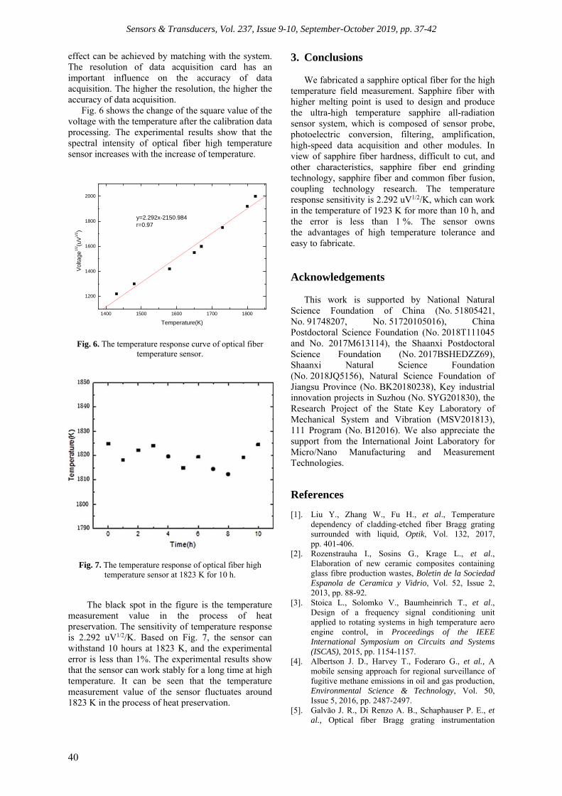
Sensors & Transducers, Vol. 237, Issue 9-10, September-October 2019, pp. 37-42
40
effect can be achieved by matching with the system. The resolution of data acquisition card has an important influence on the accuracy of data acquisition. The higher the resolution, the higher the accuracy of data acquisition.
Fig. 6 shows the change of the square value of the voltage with the temperature after the calibration data processing. The experimental results show that the spectral intensity of optical fiber high temperature sensor increases with the increase of temperature.
1400 1500 1600 1700 1800
1200
1400
1600
1800
2000
y=2.292x-2150.984r=0.97
Volta
ge1/
2 (uV
1/2 )
Temperature(K)
Fig. 6. The temperature response curve of optical fiber temperature sensor.
Fig. 7. The temperature response of optical fiber high temperature sensor at 1823 K for 10 h.
The black spot in the figure is the temperature measurement value in the process of heat preservation. The sensitivity of temperature response is 2.292 uV1/2/K. Based on Fig. 7, the sensor can withstand 10 hours at 1823 K, and the experimental error is less than 1%. The experimental results show that the sensor can work stably for a long time at high temperature. It can be seen that the temperature measurement value of the sensor fluctuates around 1823 K in the process of heat preservation.
3. Conclusions
We fabricated a sapphire optical fiber for the high temperature field measurement. Sapphire fiber with higher melting point is used to design and produce the ultra-high temperature sapphire all-radiation sensor system, which is composed of sensor probe, photoelectric conversion, filtering, amplification, high-speed data acquisition and other modules. In view of sapphire fiber hardness, difficult to cut, and other characteristics, sapphire fiber end grinding technology, sapphire fiber and common fiber fusion, coupling technology research. The temperature response sensitivity is 2.292 uV1/2/K, which can work in the temperature of 1923 K for more than 10 h, and the error is less than 1 %. The sensor owns the advantages of high temperature tolerance and easy to fabricate. Acknowledgements
This work is supported by National Natural Science Foundation of China (No. 51805421, No. 91748207, No. 51720105016), China Postdoctoral Science Foundation (No. 2018T111045 and No. 2017M613114), the Shaanxi Postdoctoral Science Foundation (No. 2017BSHEDZZ69), Shaanxi Natural Science Foundation (No. 2018JQ5156), Natural Science Foundation of Jiangsu Province (No. BK20180238), Key industrial innovation projects in Suzhou (No. SYG201830), the Research Project of the State Key Laboratory of Mechanical System and Vibration (MSV201813), 111 Program (No. B12016). We also appreciate the support from the International Joint Laboratory for Micro/Nano Manufacturing and Measurement Technologies.
References [1]. Liu Y., Zhang W., Fu H., et al., Temperature
dependency of cladding-etched fiber Bragg grating surrounded with liquid, Optik, Vol. 132, 2017, pp. 401-406.
[2]. Rozenstrauha I., Sosins G., Krage L., et al., Elaboration of new ceramic composites containing glass fibre production wastes, Boletin de la Sociedad Espanola de Ceramica y Vidrio, Vol. 52, Issue 2, 2013, pp. 88-92.
[3]. Stoica L., Solomko V., Baumheinrich T., et al., Design of a frequency signal conditioning unit applied to rotating systems in high temperature aero engine control, in Proceedings of the IEEE International Symposium on Circuits and Systems (ISCAS), 2015, pp. 1154-1157.
[4]. Albertson J. D., Harvey T., Foderaro G., et al., A mobile sensing approach for regional surveillance of fugitive methane emissions in oil and gas production, Environmental Science & Technology, Vol. 50, Issue 5, 2016, pp. 2487-2497.
[5]. Galvão J. R., Di Renzo A. B., Schaphauser P. E., et al., Optical fiber Bragg grating instrumentation
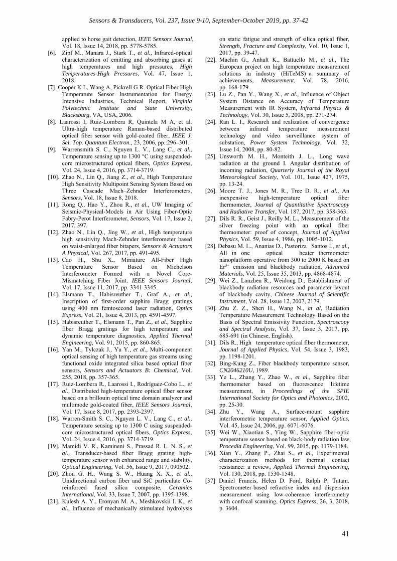
Sensors & Transducers, Vol. 237, Issue 9-10, September-October 2019, pp. 37-42
41
applied to horse gait detection, IEEE Sensors Journal, Vol. 18, Issue 14, 2018, pp. 5778-5785.
[6]. Zipf M., Manara J., Stark T., et al., Infrared-optical characterization of emitting and absorbing gases at high temperatures and high pressures, High Temperatures-High Pressures, Vol. 47, Issue 1, 2018.
[7]. Cooper K L, Wang A, Pickrell G R. Optical Fiber High Temperature Sensor Instrumentation for Energy Intensive Industries, Technical Report, Virginia Polytechnic Institute and State University, Blacksburg, VA, USA, 2006.
[8]. Laarossi I, Ruiz-Lombera R, Quintela M A, et al. Ultra-high temperature Raman-based distributed optical fiber sensor with gold-coated fiber, IEEE J. Sel. Top. Quantum Electron., 23, 2006, pp.:296–301.
[9]. Warrensmith S. C., Nguyen L. V., Lang C., et al., Temperature sensing up to 1300 °C using suspended-core microstructured optical fibers, Optics Express, Vol. 24, Issue 4, 2016, pp. 3714-3719.
[10]. Zhao N., Lin Q., Jiang Z., et al., High Temperature High Sensitivity Multipoint Sensing System Based on Three Cascade Mach–Zehnder Interferometers, Sensors, Vol. 18, Issue 8, 2018.
[11]. Rong Q., Hao Y., Zhou R., et al., UW Imaging of Seismic-Physical-Models in Air Using Fiber-Optic Fabry-Perot Interferometer, Sensors, Vol. 17, Issue 2, 2017, 397.
[12]. Zhao N., Lin Q., Jing W., et al., High temperature high sensitivity Mach-Zehnder interferometer based on waist-enlarged fiber bitapers, Sensors & Actuators A Physical, Vol. 267, 2017, pp. 491-495.
[13]. Cao H., Shu X., Miniature All-Fiber High Temperature Sensor Based on Michelson Interferometer Formed with a Novel Core-Mismatching Fiber Joint, IEEE Sensors Journal, Vol. 17, Issue 11, 2017, pp. 3341-3345.
[14]. Elsmann T., Habisreuther T., Graf A., et al., Inscription of first-order sapphire Bragg gratings using 400 nm femtosecond laser radiation, Optics Express, Vol. 21, Issue 4, 2013, pp. 4591-4597.
[15]. Habisreuther T., Elsmann T., Pan Z., et al., Sapphire fiber Bragg gratings for high temperature and dynamic temperature diagnostics, Applied Thermal Engineering, Vol. 91, 2015, pp. 860-865.
[16]. Yan M., Tylczak J., Yu Y., et al., Multi-component optical sensing of high temperature gas streams using functional oxide integrated silica based optical fiber sensors, Sensors and Actuators B: Chemical, Vol. 255, 2018, pp. 357-365.
[17]. Ruiz-Lombera R., Laarossi I., Rodríguez-Cobo L., et al., Distributed high-temperature optical fiber sensor based on a brillouin optical time domain analyzer and multimode gold-coated fiber, IEEE Sensors Journal, Vol. 17, Issue 8, 2017, pp. 2393-2397.
[18]. Warren-Smith S. C., Nguyen L. V., Lang C., et al., Temperature sensing up to 1300 C using suspended-core microstructured optical fibers, Optics Express, Vol. 24, Issue 4, 2016, pp. 3714-3719.
[19]. Mamidi V. R., Kamineni S., Prassad R. L. N. S., et al., Transducer-based fiber Bragg grating high-temperature sensor with enhanced range and stability, Optical Engineering, Vol. 56, Issue 9, 2017, 090502.
[20]. Zhou G. H., Wang S. W., Huang X. X., et al., Unidirectional carbon fiber and SiC particulate Co-reinforced fused silica composite, Ceramics International, Vol. 33, Issue 7, 2007, pp. 1395-1398.
[21]. Kulesh A. Y., Eronyan M. A., Meshkovskii I. K., et al., Influence of mechanically stimulated hydrolysis
on static fatigue and strength of silica optical fiber, Strength, Fracture and Complexity, Vol. 10, Issue 1, 2017, pp. 39-47.
[22]. Machin G., Anhalt K., Battuello M., et al., The European project on high temperature measurement solutions in industry (HiTeMS)–a summary of achievements, Measurement, Vol. 78, 2016, pp. 168-179.
[23]. Lu Z., Pan Y., Wang X., et al., Influence of Object System Distance on Accuracy of Temperature Measurement with IR System, Infrared Physics & Technology, Vol. 30, Issue 5, 2008, pp. 271-274.
[24]. Ran L. I., Research and realization of convergence between infrared temperature measurement technology and video surveillance system of substation, Power System Technology, Vol. 32, Issue 14, 2008, pp. 80-82.
[25]. Unsworth M. H., Monteith J. L., Longwave radiation at the ground I. Angular distribution of incoming radiation, Quarterly Journal of the Royal Meteorological Society, Vol. 101, Issue 427, 1975, pp. 13-24.
[26]. Moore T. J., Jones M. R., Tree D. R., et al., An inexpensive high-temperature optical fiber thermometer, Journal of Quantitative Spectroscopy and Radiative Transfer, Vol. 187, 2017, pp. 358-363.
[27]. Dils R. R., Geist J., Reilly M. L., Measurement of the silver freezing point with an optical fiber thermometer: proof of concept, Journal of Applied Physics, Vol. 59, Issue 4, 1986, pp. 1005-1012.
[28]. Debasu M. L., Ananias D., PastorizaSantos I., et al., Allinone optical heaterthermometer nanoplatform operative from 300 to 2000 K based on Er3+ emission and blackbody radiation, Advanced Materials, Vol. 25, Issue 35, 2013, pp. 4868-4874.
[29]. Wei Z., Lanzhen R., Weidong D., Establishment of blackbody radiation resources and parameter layout of blackbody cavity, Chinese Journal of Scientific Instrument, Vol. 28, Issue 12, 2007, 2179.
[30]. Zhu Z. Z., Shen H., Wang N., at al, Radiation Temperature Measurement Technology Based on the Basis of Spectral Emissivity Function, Spectroscopy and Spectral Analysis, Vol. 37, Issue 3, 2017, pp. 685-691 (in Chinese, English).
[31]. Dils R., Hightemperature optical fiber thermometer, Journal of Applied Physics, Vol. 54, Issue 3, 1983, pp. 1198-1201.
[32]. Bing-Kung Z., Fiber blackbody temperature sensor, CN2046210U, 1989.
[33]. Ye L., Zhang Y., Zhao W., et al., Sapphire fiber thermometer based on fluorescence lifetime measurement, in Proceedings of the SPIE International Society for Optics and Photonics, 2002, pp. 25-30.
[34]. Zhu Y., Wang A., Surface-mount sapphire interferometric temperature sensor, Applied Optics, Vol. 45, Issue 24, 2006, pp. 6071-6076.
[35]. Wei W., Xiaotian S., Ying W., Sapphire fiber-optic temperature sensor based on black-body radiation law, Procedia Engineering, Vol. 99, 2015, pp. 1179-1184.
[36]. Xian Y., Zhang P., Zhai S., et al., Experimental characterization methods for thermal contact resistance: a review, Applied Thermal Engineering, Vol. 130, 2018, pp. 1530-1548.
[37] Daniel Francis, Helen D. Ford, Ralph P. Tatam. Spectrometer-based refractive index and dispersion measurement using low-coherence interferometry with confocal scanning, Optics Express, 26, 3, 2018, p. 3604.

Sensors & Transducers, Vol. 237, Issue 9-10, September-October 2019, pp. 37-42
42
[38]. Guo Y., Xia W., Hu Z., et al., High-temperature sensor instrumentation with a thin-film-based sapphire fiber, Applied Optics, Vol. 56, Issue 8, 2017, pp. 2068-2073.
[39]. Ye L., Shen Z., Tong L., et al., Optical properties of sapphire fiber under high temperature, SPIE Proceedings. Advanced Materials and Devices for Sensing and Imaging, Vol. 4919, 2002, pp. 161-166.
[40]. Chao W., Fanxue B., Shoufeng T., et al., Coupling Efficiency and Influencing Factors of Space Light to Less Modular Fiber, Photon Journal, Vol. 47, Issue 12, 2018, pp. 1206001-1206001.
[41]. Haozhongyang C., Jinsong N., Study on Bending Loss of Guidance Fiber, Infrared and Laser Engineering, Vol. 25, 2006, pp. 1-5.
[42]. Lishan G., Xiaoping C., Study on optical fiber beam transmission rate measurement method, Journal of Electronic Surveying and Instrument, Vol. 29, Issue 8, 2015, pp. 1231-1235.
[43]. Li C., Wei H., Zhao Y., et al., Laser-Assisted Permeation of Titanium Dioxide Nanoparticles in Ex Vivo Human Endometrium Tissues Monitored by OCT and Diffuse Reflectance Spectra, IEEE Journal of Selected Topics in Quantum Electronics, Vol. 25, Issue 2, 2018, pp. 1-9.
[44]. Na Z., Qijing L., Zhuangde J., Kun Y., Bian T., Zhongkai Z., Sapphire optical fiber sensor for ultra high temperature measurement, in Proceedings of the 5th International Conference on Sensors and Electronic Instrumentation Advances (SEIA'2019), Adeje, Tenerife (Canary Islands), Spain, 25-27 September 2019, pp.257-260.
[45]. Ogarev S., Khlevnoi B., Samoilov M., et al., High-temperature blackbody models for use in photometry, radiometry, and radiation thermometry, Measurement Techniques, Vol. 58, Issue 11, 2016, pp. 1255-1260.
__________________
Published by International Frequency Sensor Association (IFSA) Publishing, S. L., 2019 (http://www.sensorsportal.com).

Sensors & Transducers, Vol. 237, Issue 9-10, September-October 2019, pp. 43-51
43
Sensors & Transducers
Published by IFSA Publishing, S. L., 2019 http://www.sensorsportal.com
Micro-structured Optical Spectrometer Sensor in PMMA
1, * Fischer-Hirchert Ulrich H. P., 2 Höll Sebastian, 1.Haupt Matthias and 3 Joncic Mladen
1 Harz University of Applied Sciences, Friedrichstr. 57, 38855 Wernigerode, Germany 2 Sicoya GmbH, Carl-Scheele-Straße 16, 12489 Berlin, Germany
3 IAV GmbH, Carnotstraße 1, 10587 Berlin Tel.: + 49 3943659 351, fax: + 49 3943659 5351
E-mail: [email protected]
Received: 30 August 2019 /Accepted: 27 September 2019 /Published: 30 November 2019 Abstract: Data communication over Polymer Optical Fibers (POF) is limited to only one channel for data transmission. Therefore the bandwidth is strongly restricted. By using more than one channel, it is possible to break through the limit. This technique is called Wavelength Division Multiplexing (WDM). It uses different wavelengths in the visible spectrum to transmit data parallel over one fiber. Two components are essential for this technology: A multiplexer (MUX) and a demultiplexer (DEMUX). The multiplexer collects the light of the different sources to one fiber and the demultiplexer separates the light at the end of the fiber into the different fiber output ports. In this paper, we show the realization of a grating spectrometer realised by injection moulding in PMMA, working in the visible spectrum, respectively. We present the results of a demonstrator of an integrated polymeric spectrometer device produced with injection moulding in combination with hot embossing. The paper discusses the results of the different development steps, the measurements done with the first demonstrator and the challenges related to the injection moulding process. Keywords: Optical spectrum analyzer, PMMA injection moulded optical spectrum sensor, Hot embossing sensor, Polymeric fiber WDM systems, POF over WDM. 1. Introduction
Polymer Optical Fibers (POF) are used in various fields of applications. The core material consists of PMMA (Polymethylmethacrylate), while the cover is made of fluorinated PMMA. The whole fiber has a diameter of 1 mm. POFs are used for optical data transmission based on the same principle as glass fiber. As a communication medium they offer a couple of advantages related to other data communication systems such as copper cables, glass fibers and wireless systems, and have great potential to replace them in different applications.
Namely, in comparison with glass fibres (GOF), POFs have the advantage of easy and economical
processing and are more flexible for optical connections [1]. However, one advantage of using glass fibres is their low attenuation, which is below 0.2 dB/km in the infrared range. The larger core diameter of POFs leads to higher mode dispersion and thus to higher attenuation across the electromagnetic spectrum. This increased attenuation leaves only one remaining transmission window, namely the visible spectrum of light (400 – 700 nm). Hence, POFs are best suited for the use in short distance data communication.
Here, POFs can outperform the current standard of copper cable as communication medium. On the one hand, they feature lower weight and space. On the other hand, POFs are not susceptible to
http://www.sensorsportal.com/HTML/DIGEST/P_3109.htm
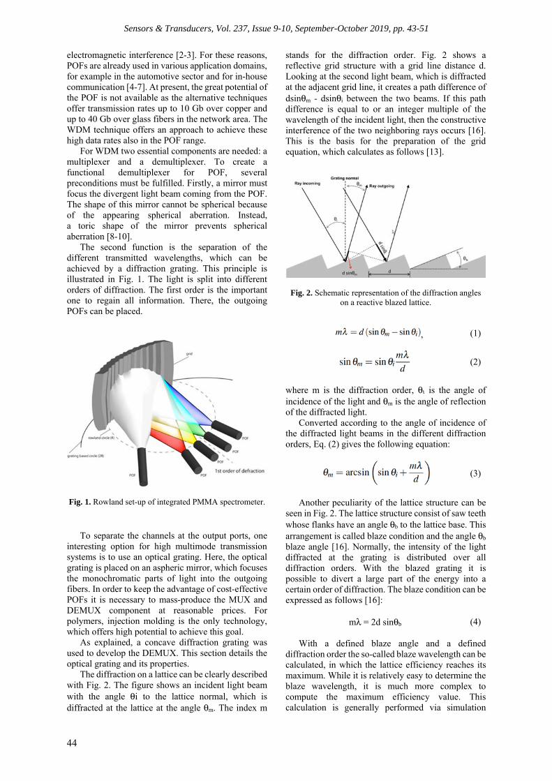
Sensors & Transducers, Vol. 237, Issue 9-10, September-October 2019, pp. 43-51
44
electromagnetic interference [2-3]. For these reasons, POFs are already used in various application domains, for example in the automotive sector and for in-house communication [4-7]. At present, the great potential of the POF is not available as the alternative techniques offer transmission rates up to 10 Gb over copper and up to 40 Gb over glass fibers in the network area. The WDM technique offers an approach to achieve these high data rates also in the POF range.
For WDM two essential components are needed: a multiplexer and a demultiplexer. To create a functional demultiplexer for POF, several preconditions must be fulfilled. Firstly, a mirror must focus the divergent light beam coming from the POF. The shape of this mirror cannot be spherical because of the appearing spherical aberration. Instead, a toric shape of the mirror prevents spherical aberration [8-10].
The second function is the separation of the different transmitted wavelengths, which can be achieved by a diffraction grating. This principle is illustrated in Fig. 1. The light is split into different orders of diffraction. The first order is the important one to regain all information. There, the outgoing POFs can be placed.
Fig. 1. Rowland set-up of integrated PMMA spectrometer.
To separate the channels at the output ports, one interesting option for high multimode transmission systems is to use an optical grating. Here, the optical grating is placed on an aspheric mirror, which focuses the monochromatic parts of light into the outgoing fibers. In order to keep the advantage of cost-effective POFs it is necessary to mass-produce the MUX and DEMUX component at reasonable prices. For polymers, injection molding is the only technology, which offers high potential to achieve this goal.
As explained, a concave diffraction grating was used to develop the DEMUX. This section details the optical grating and its properties.
The diffraction on a lattice can be clearly described with Fig. 2. The figure shows an incident light beam with the angle θi to the lattice normal, which is diffracted at the lattice at the angle θm. The index m
stands for the diffraction order. Fig. 2 shows a reflective grid structure with a grid line distance d. Looking at the second light beam, which is diffracted at the adjacent grid line, it creates a path difference of dsinθm - dsinθi between the two beams. If this path difference is equal to or an integer multiple of the wavelength of the incident light, then the constructive interference of the two neighboring rays occurs [16]. This is the basis for the preparation of the grid equation, which calculates as follows [13].
Fig. 2. Schematic representation of the diffraction angles on a reactive blazed lattice.
, (1)
(2)
where m is the diffraction order, θι is the angle of incidence of the light and θm is the angle of reflection of the diffracted light.
Converted according to the angle of incidence of the diffracted light beams in the different diffraction orders, Eq. (2) gives the following equation:
(3)
Another peculiarity of the lattice structure can be
seen in Fig. 2. The lattice structure consist of saw teeth whose flanks have an angle θb to the lattice base. This arrangement is called blaze condition and the angle θb blaze angle [16]. Normally, the intensity of the light diffracted at the grating is distributed over all diffraction orders. With the blazed grating it is possible to divert a large part of the energy into a certain order of diffraction. The blaze condition can be expressed as follows [16]:
mλ = 2d sinθb (4)
With a defined blaze angle and a defined
diffraction order the so-called blaze wavelength can be calculated, in which the lattice efficiency reaches its maximum. While it is relatively easy to determine the blaze wavelength, it is much more complex to compute the maximum efficiency value. This calculation is generally performed via simulation

Sensors & Transducers, Vol. 237, Issue 9-10, September-October 2019, pp. 43-51
45
programs (e.g., OpTaliX) and simulates the course of lattice efficiency in a selected wavelength range. Since the transmission window is in the wavelength range of 400 - 700 nm, it is expedient to place the blaze wavelength approximately in the middle. The best lattice over the wavelength range can be achieved with λb = 518.5 nm. The course of the effectivity and the simulation results of the grid are summarized in [23-24]. With the blaze wavelength being in the second diffraction order, the blaze angle can be calculated to be θb = 11.97°.
A very important parameter for the properties of the DEMUX is the angular dispersion. For a fixed angle of incidence qi this means the change of the angle θm as a function of the wavelength λ of the incident light, i.e. the quantity ∂θm/∂λ.
The greater the angular dispersion, the stronger the spectral splitting, the further apart the interference maxima for light waves of different wavelengths are. A large angular dispersion is a prerequisite for a large spectral resolution. By deriving the lattice Eq. (2) by the wavelength and at a constant angle of incidence qi, the angle dispersion results to [13]:
(5)
Since the DEMUX is a component made of
transparent plastic, the light from the POF is completely guided in the material of the DEMUX. Consequently, there is no transition from PMMA (core of the POF) to air. First, this results in the Numerical Aperture (NA) of the fiber being reduced to e.g. PMMA to PMMA-DEMUX: NA = 0.34. Second, the wavelength of the light, when it enters another medium (other than air or vacuum), changes to:
λM =λ/nM(λ) (6)
where λM is the wavelength of the light in the medium, λ is the wavelength of the light in the vacuum and nM (λ) is the wavelength-dependent refractive index of the medium. It can be seen that with a refractive index > 1 the wavelength shortens. This must be taken into account when considering the grid equation for the wavelengths to be transmitted.
2. Production Method for Concave Lattice Structures
2.1. Micromechanical Fabrication Methods
As emerged from the previous sections, a 3-
dimensional approach to the DEMUX element must be determined. The challenge is to fabricate the device with a concave, 3-dimensional, micro structured diffraction grating, which also has the function of positioning and combining the input and output fibers. This includes photolithographic production methods and LIGA (acronym for lithography, electroplating
and impression taking) [17], which are largely established in the manufacture of MEMS components (micro-electro-mechanical systems), but for the production of the DEMUX unsuitable. Although these are characterized by smaller structure sizes and the high production rate due to batch processes. Unfortunately, they are limited to planar component geometries with a maximum of 2.5 dimensions.
On the other hand, mechanical micromachining brings many advantages in terms of making the DEMUX. Among other things, these include the creation of complex geometries, higher relative accuracies and greater freedom in the choice of component material. A comparison between MEMS-based manufacturing methods and mechanical micromachining is shown in Table 1.
Table 1. Comparison between MEMS processes and micromachining processes
MEMS process Micromachining
Edit. material
Silicon, some metals
Metals, alloys, plastics,
ceramics, glasses Component geometry Planar to 2.5D 3D
Rel. accuracy 10-1 - 10-3 10-3 - 10-5
Process control Feedforward Feedback
Production volume High High or low
Production rate High Small
Total investment High Medium to small
Applications
MEMS, microelectronics
planar microcomponents
Various 3D microcomponents
Furthermore, the methods of micromachining can be classified according to their underlying mechanisms. It differs physical, chemical and mechanical removal mechanisms. The mechanical processes are divided into cutting and abrasive methods.
These are subdivided into grinding and polishing for the abrasives and diamond turning and diamond milling in the area of cutting processes. Diamond turning and milling are known as ultra-precision machining. This technique is discussed in more detail in the next section.
2.2. Ultra-precision Machining Ultra-Precision Machining (UPB) is a machining
with a diamond tool. Only a very small layer of the surface is removed, but this with the highest precision. Ultra-precision machining is one of the most important techniques for producing high-precision

Sensors & Transducers, Vol. 237, Issue 9-10, September-October 2019, pp. 43-51
46
components with surface roughnesses of a few nanometers (1-10 nm) and tolerance deviations in the sub-micron range. Spherical and aspherical surfaces can be produced with high optical quality. [19-20] Optical precision can only be achieved by using extremely high-precision mechanical positioning systems become. Today's systems achieve exceptionally high mechanical precision and stability [19].
Before starting the production of the mold insert, a demonstrator of the DEMUX is fabricated by directly machining it in the PMMA material by means of diamond turning technique (see Fig. 3). Thus, the same diamond-turning technology is used for the manufacture of the mold insert. This step is done due to validate the simulation results with the produced component.
The UPB offers several advantages when creating the optical DEMUX:
- Real 3D structure creation; - Production of optical surfaces up to the edge of
the element with roughness in the single-digit nanometer range;
- Components with variable aspect ratios can be realized;
- Machining soft ductile materials which are difficult to polish;
- Possibility to integrate adjustment elements; - Production of forms, which are difficult to reach
with other methods.
Fig. 3. Prototype of integrated PMMA spectrometer.
UPB is often used for the prototype production of PMMA lens surfaces. Experimental results show that during processing of PMMA, there is little variation in dynamic cutting force and continuous chip formation. This is very beneficial for the machining of micro and nanostructures. The amorphous and ductile nature of PMMA makes it possible to directly cut optically qualitative surfaces without any post-processing.
For this reason, it is not possible, according to the state of the art, to use UPB directly to produce hardened steel injection molds, which is the preferred material for producing tools. The production therefore takes place in two steps. The first step is to create a
structure in steel that approximates the natal structure. Then a thin Layer (up to 500 mm) nickel chemically (electroless) deposited on the steel surface. In the second step, the male structure is introduced into the nickel layer by means of UPB. In this way, the resistance to the high pressures during injection molding (sometimes more than 1000 bar [22]) can be greatly increased. [21].
3. Manufacturing of the Demonstrator
The selection of a suitable material for the production of an optical system depends on various criteria:
- Optical properties; - Mechanical properties; - Thermal and thermomechanical properties; - Resistance to environmental influences; - Availability and costs. That all these features are considered in one
application is rare. Typically, different applications only require the evaluation of one to two criteria. For example, transmissive components are chosen for their optical properties, while reactive components are distinguished by their mechanical and thermal properties. Materials used for the injection molding of optical components must meet high thermal requirements and be resistant to external environments (e.g., high pressure).
The number of materials that can be processed with UPB is increasing continuously. An excerpt from the most important workable materials is the following list:
- Aluminum alloys (1100, 2011, 2017, 2024, 3003, 5086, 5186, 6061, 7075); - Brass; - Copper (OFHC-Oxygen free high conductivity copper, galvanic copper, Alloys with beryllium); - Gold; - Nickel (chemically with 10-12% phosphorus content); - Silver; - Tin; - Zinc; - Polymethylmetacylate (PMMA); - Polycarbonate (PC). Not all of these materials are equally well suited
for diamond machining. Optimum manufacturing parameters (e.g., rotational speeds and feed, coolant, and tool condition) are very different for each material. Some of these materials are preferred in terms of the ability to produce optically smooth and geometry-stable surfaces with the UPB. Among the metals are: aluminum, copper, galvanic copper and chemical nickel.
PMMA is the best material to process among the polymers.
By using the injection molding process, the manufacturing of the mold insert is the most important factor. Due to the three-dimensional toric structure of the grating planar manufacturing methods like

Sensors & Transducers, Vol. 237, Issue 9-10, September-October 2019, pp. 43-51
47
lithography, especially LIGA cannot be used. LIGA is used to manufacture planar spectrometers based on the glass fiber technology [11-14]. But in our case, the three-dimensional grating needs another machining method. Especially the microstructure of the grating and the exact curve shape of the toric surface require high precision.
The microstructure has the shape of a saw tooth with a pitch between the teeth of 2.5 µm. Fig. 4 shows an enlarged 3D-Model of the grating. After investigate several machining methods only the diamond turning meets the high demands of the micro structured grating.
Fig. 4. 3D Sawtooth like simulation of the grating of the prototype.
4. Transmission Measurements
Prior to the production of the DEMUX some preliminary investigations have taken place to find the best suitable material for the demultiplexer. Therefore, both the processability of the material and the optical parameters had to be considered in detail. The injection molding process was tested with a thick-walled mold (see Fig. 5).
This test tool had the same shape as the final DEMUX, except for the grid. The test runs were carried out with an injection-molding machine from Babyplast 6-10P. This device was able to inject precisely small parts. Table 2 lists all the materials used for the study. Further parameters such as the respective melt volume rate (MVR) and light transmittance (according to the manufacturer's specification) are depicted. The test was additionally used to find the optimized injection molding process parameters for the material.
In addition, the optical quality of the polymer materials must be investigated. Therefore, a mold for injection molding test plates was designed. The test plates had a thickness of 2 mm. The mold is used to make samples from each material listed in Table 2. The DIN EN ISO 13468-2 standard describes the measurement of the optical transmission of polymer materials. Therefore, the test plates are designed to meet this standard.
Transmission measurements were carried out with all test plates. The results are shown for 405 nm in Fig. 6. It can be seen that both ZEONEX types and PMMA POQ62 show the highest value for the light transmission. PMMA POQ62 is a polymer grade with high purity of polymer granulates. The measurement is made at a wavelength of 405 nm because it is one of the wavelengths used for the WDM system. [18].
Fig. 5. Molded part of the sample plates made of PMMA.
Fig. 6. Transmission of different material at 405 nm.
Table 2. Injection molding materials for the integrated spectrometer element.
Name Type MVR [cm³/10min]
Transmission [%]
Plexiglas 6N PMMA 12 92
Plexiglas POQ62
PMMA 21 92
Topas 5013L-10 COC 48 91.4
Topas 6013M-07 COC 14 91
ZEONEX F52R COP 22 92
ZEONEX 350R COP 26 92
Makrolon LED2245
PC 35 90
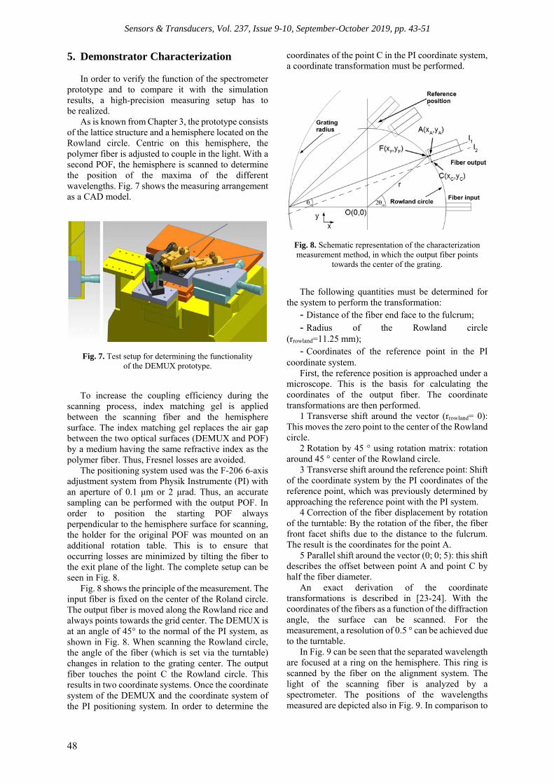
Sensors & Transducers, Vol. 237, Issue 9-10, September-October 2019, pp. 43-51
48
5. Demonstrator Characterization In order to verify the function of the spectrometer
prototype and to compare it with the simulation results, a high-precision measuring setup has to be realized.
As is known from Chapter 3, the prototype consists of the lattice structure and a hemisphere located on the Rowland circle. Centric on this hemisphere, the polymer fiber is adjusted to couple in the light. With a second POF, the hemisphere is scanned to determine the position of the maxima of the different wavelengths. Fig. 7 shows the measuring arrangement as a CAD model.
Fig. 7. Test setup for determining the functionality of the DEMUX prototype.
To increase the coupling efficiency during the scanning process, index matching gel is applied between the scanning fiber and the hemisphere surface. The index matching gel replaces the air gap between the two optical surfaces (DEMUX and POF) by a medium having the same refractive index as the polymer fiber. Thus, Fresnel losses are avoided.
The positioning system used was the F-206 6-axis adjustment system from Physik Instrumente (PI) with an aperture of 0.1 μm or 2 μrad. Thus, an accurate sampling can be performed with the output POF. In order to position the starting POF always perpendicular to the hemisphere surface for scanning, the holder for the original POF was mounted on an additional rotation table. This is to ensure that occurring losses are minimized by tilting the fiber to the exit plane of the light. The complete setup can be seen in Fig. 8.
Fig. 8 shows the principle of the measurement. The input fiber is fixed on the center of the Roland circle. The output fiber is moved along the Rowland rice and always points towards the grid center. The DEMUX is at an angle of 45° to the normal of the PI system, as shown in Fig. 8. When scanning the Rowland circle, the angle of the fiber (which is set via the turntable) changes in relation to the grating center. The output fiber touches the point C the Rowland circle. This results in two coordinate systems. Once the coordinate system of the DEMUX and the coordinate system of the PI positioning system. In order to determine the
coordinates of the point C in the PI coordinate system, a coordinate transformation must be performed.
Fig. 8. Schematic representation of the characterization measurement method, in which the output fiber points
towards the center of the grating.
The following quantities must be determined for the system to perform the transformation:
- Distance of the fiber end face to the fulcrum; - Radius of the Rowland circle
(rrowland=11.25 mm); - Coordinates of the reference point in the PI
coordinate system. First, the reference position is approached under a
microscope. This is the basis for calculating the coordinates of the output fiber. The coordinate transformations are then performed.
1 Transverse shift around the vector (rrowland= 0): This moves the zero point to the center of the Rowland circle.
2 Rotation by 45 ° using rotation matrix: rotation around 45 ° center of the Rowland circle.
3 Transverse shift around the reference point: Shift of the coordinate system by the PI coordinates of the reference point, which was previously determined by approaching the reference point with the PI system.
4 Correction of the fiber displacement by rotation of the turntable: By the rotation of the fiber, the fiber front facet shifts due to the distance to the fulcrum. The result is the coordinates for the point A.
5 Parallel shift around the vector (0; 0; 5): this shift describes the offset between point A and point C by half the fiber diameter.
An exact derivation of the coordinate transformations is described in [23-24]. With the coordinates of the fibers as a function of the diffraction angle, the surface can be scanned. For the measurement, a resolution of 0.5 ° can be achieved due to the turntable.
In Fig. 9 can be seen that the separated wavelength are focused at a ring on the hemisphere. This ring is scanned by the fiber on the alignment system. The light of the scanning fiber is analyzed by a spectrometer. The positions of the wavelengths measured are depicted also in Fig. 9. In comparison to

Sensors & Transducers, Vol. 237, Issue 9-10, September-October 2019, pp. 43-51
49
the simulation a shift of the positions can be recognized. Nevertheless, the separation of the wavelengths was measured and confirms the functionality of the demultiplexer.
Fig. 9. Measurement results of the focal points for different wavelengths (405 nm violet ray; 450 nm blue ray;
520 nm green ray; 650 nm red ray.
6. Manufacturing of the Demonstrator By using the injection molding process, the
manufacturing of the mold insert is the most important factor. Due to the three-dimensional toric structure of the grating planar manufacturing methods like lithography, especially LIGA cannot be used [14].
The microstructure has the shape of a sawtooth with a distance between the teeth of 2.5 μm. Fig. 4 shows an enlarged 3D model of the grating. An in-depth investigation of various processing methods has shown that only the diamond turning fulfills the high requirements of the production of the microstructural lattice. The diamond twisting technique is a special machining method using a single crystal diamond-cutting tool. It is also possible to produce a surface with an optical quality at the edge of the optical component. It offers several advantages:
- True three-dimensional contour generation; - Accuracy of one part in 106 with absolute
accuracy of 1 part in 108 on a single axis for ideal conditions;
- Surface finish of 5 nm Ra for a range of materials and as good as 1 nm Rz;
- Ability to generate surfaces with variable aspect ratios, and
- Feature sizes that exceed the limits of optical microscopy [11-14].
A metallization process was used to analyze the surface of the lattice. The surface was sputtered with a thin aluminum layer depicted in Fig. 10. It is now possible to measure the shape of the surface with a white light interferometer and to examine the lattice structure under the scanning electron microscope (SEM).
Fig. 10. High quality structures of the grating.
The metallized surface of the grating is shown in Fig. 10. It can be seen that the structure on the left side has a dull and mat surface instead of the glossy residue of the surface. This is a first indication that the surface roughness in this part is higher and does not meet the requirements for the component precision. The first visual impression was then confirmed by the analysis under the SEM which is depicted in Fig. 11.
Fig. 11. SEM photographs of the structures of the grating at different locations.
The grid quality is excellent in the first half of the grid. From half of the quality deteriorates and ultimately merges into the dull, unstructured area at the edge. Above all, however, the grid line spacing, as in Table 3, is within the required tolerance.
On the other hand, improvements in the area of the radii of the grid and the grid height still have to be made. As shown in Table 3, these are still too low. Furthermore, the packaging and handling of the
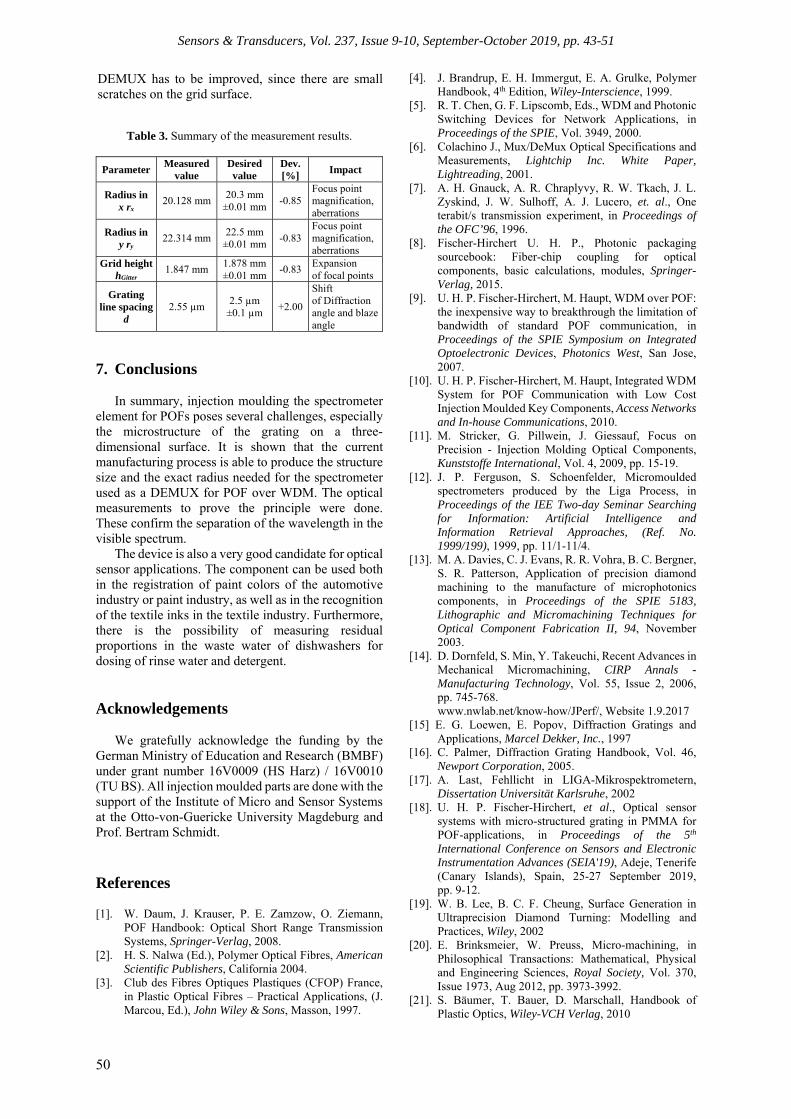
Sensors & Transducers, Vol. 237, Issue 9-10, September-October 2019, pp. 43-51
50
DEMUX has to be improved, since there are small scratches on the grid surface.
Table 3. Summary of the measurement results.
Parameter Measured value
Desired value
Dev. [%] Impact
Radius in x rx 20.128 mm
20.3 mm ±0.01 mm
-0.85 Focus point magnification, aberrations
Radius in y ry 22.314 mm
22.5 mm ±0.01 mm
-0.83 Focus point magnification, aberrations
Grid height hGitter 1.847 mm
1.878 mm ±0.01 mm
-0.83 Expansion of focal points
Grating line spacing
d 2.55 µm
2.5 µm ±0.1 µm
+2.00
Shift of Diffraction angle and blaze angle
7. Conclusions In summary, injection moulding the spectrometer
element for POFs poses several challenges, especially the microstructure of the grating on a three-dimensional surface. It is shown that the current manufacturing process is able to produce the structure size and the exact radius needed for the spectrometer used as a DEMUX for POF over WDM. The optical measurements to prove the principle were done. These confirm the separation of the wavelength in the visible spectrum.
The device is also a very good candidate for optical sensor applications. The component can be used both in the registration of paint colors of the automotive industry or paint industry, as well as in the recognition of the textile inks in the textile industry. Furthermore, there is the possibility of measuring residual proportions in the waste water of dishwashers for dosing of rinse water and detergent.
Acknowledgements We gratefully acknowledge the funding by the
German Ministry of Education and Research (BMBF) under grant number 16V0009 (HS Harz) / 16V0010 (TU BS). All injection moulded parts are done with the support of the Institute of Micro and Sensor Systems at the Otto-von-Guericke University Magdeburg and Prof. Bertram Schmidt. References [1]. W. Daum, J. Krauser, P. E. Zamzow, O. Ziemann,
POF Handbook: Optical Short Range Transmission Systems, Springer-Verlag, 2008.
[2]. H. S. Nalwa (Ed.), Polymer Optical Fibres, American Scientific Publishers, California 2004.
[3]. Club des Fibres Optiques Plastiques (CFOP) France, in Plastic Optical Fibres – Practical Applications, (J. Marcou, Ed.), John Wiley & Sons, Masson, 1997.
[4]. J. Brandrup, E. H. Immergut, E. A. Grulke, Polymer Handbook, 4th Edition, Wiley-Interscience, 1999.
[5]. R. T. Chen, G. F. Lipscomb, Eds., WDM and Photonic Switching Devices for Network Applications, in Proceedings of the SPIE, Vol. 3949, 2000.
[6]. Colachino J., Mux/DeMux Optical Specifications and Measurements, Lightchip Inc. White Paper, Lightreading, 2001.
[7]. A. H. Gnauck, A. R. Chraplyvy, R. W. Tkach, J. L. Zyskind, J. W. Sulhoff, A. J. Lucero, et. al., One terabit/s transmission experiment, in Proceedings of the OFC’96, 1996.
[8]. Fischer-Hirchert U. H. P., Photonic packaging sourcebook: Fiber-chip coupling for optical components, basic calculations, modules, Springer-Verlag, 2015.
[9]. U. H. P. Fischer-Hirchert, M. Haupt, WDM over POF: the inexpensive way to breakthrough the limitation of bandwidth of standard POF communication, in Proceedings of the SPIE Symposium on Integrated Optoelectronic Devices, Photonics West, San Jose, 2007.
[10]. U. H. P. Fischer-Hirchert, M. Haupt, Integrated WDM System for POF Communication with Low Cost Injection Moulded Key Components, Access Networks and In-house Communications, 2010.
[11]. M. Stricker, G. Pillwein, J. Giessauf, Focus on Precision - Injection Molding Optical Components, Kunststoffe International, Vol. 4, 2009, pp. 15-19.
[12]. J. P. Ferguson, S. Schoenfelder, Micromoulded spectrometers produced by the Liga Process, in Proceedings of the IEE Two-day Seminar Searching for Information: Artificial Intelligence and Information Retrieval Approaches, (Ref. No. 1999/199), 1999, pp. 11/1-11/4.
[13]. M. A. Davies, C. J. Evans, R. R. Vohra, B. C. Bergner, S. R. Patterson, Application of precision diamond machining to the manufacture of microphotonics components, in Proceedings of the SPIE 5183, Lithographic and Micromachining Techniques for Optical Component Fabrication II, 94, November 2003.
[14]. D. Dornfeld, S. Min, Y. Takeuchi, Recent Advances in Mechanical Micromachining, CIRP Annals - Manufacturing Technology, Vol. 55, Issue 2, 2006, pp. 745-768. www.nwlab.net/know-how/JPerf/, Website 1.9.2017
[15] E. G. Loewen, E. Popov, Diffraction Gratings and Applications, Marcel Dekker, Inc., 1997
[16]. C. Palmer, Diffraction Grating Handbook, Vol. 46, Newport Corporation, 2005.
[17]. A. Last, Fehllicht in LIGA-Mikrospektrometern, Dissertation Universität Karlsruhe, 2002
[18]. U. H. P. Fischer-Hirchert, et al., Optical sensor systems with micro-structured grating in PMMA for POF-applications, in Proceedings of the 5th International Conference on Sensors and Electronic Instrumentation Advances (SEIA'19), Adeje, Tenerife (Canary Islands), Spain, 25-27 September 2019, pp. 9-12.
[19]. W. B. Lee, B. C. F. Cheung, Surface Generation in Ultraprecision Diamond Turning: Modelling and Practices, Wiley, 2002
[20]. E. Brinksmeier, W. Preuss, Micro-machining, in Philosophical Transactions: Mathematical, Physical and Engineering Sciences, Royal Society, Vol. 370, Issue 1973, Aug 2012, pp. 3973-3992.
[21]. S. Bäumer, T. Bauer, D. Marschall, Handbook of Plastic Optics, Wiley-VCH Verlag, 2010

Sensors & Transducers, Vol. 237, Issue 9-10, September-October 2019, pp. 43-51
51
[22]. R. Mayer, Precision Injection Molding, Optik & Photonik, Vol. 2, Issue 4, 2007
[23]. M. Haupt, U. H. P. Fischer-Hirchert, Optical design of a low-loss demultiplexer for optical communication systems in the visible range, SPIE Optical Systems Design, Vol. 8550, 2012, 85500J.
[24]. S. Höll, Herstellung eines Wavelength Division Multiplex (WDM) Demultiplexer für Optische Polymerfasern (POF)m im Spritzgussverfahren, Cuvillier Verlag Göttingen, 2018
__________________
Published by International Frequency Sensor Association (IFSA) Publishing, S. L., 2019 (http://www.sensorsportal.com).
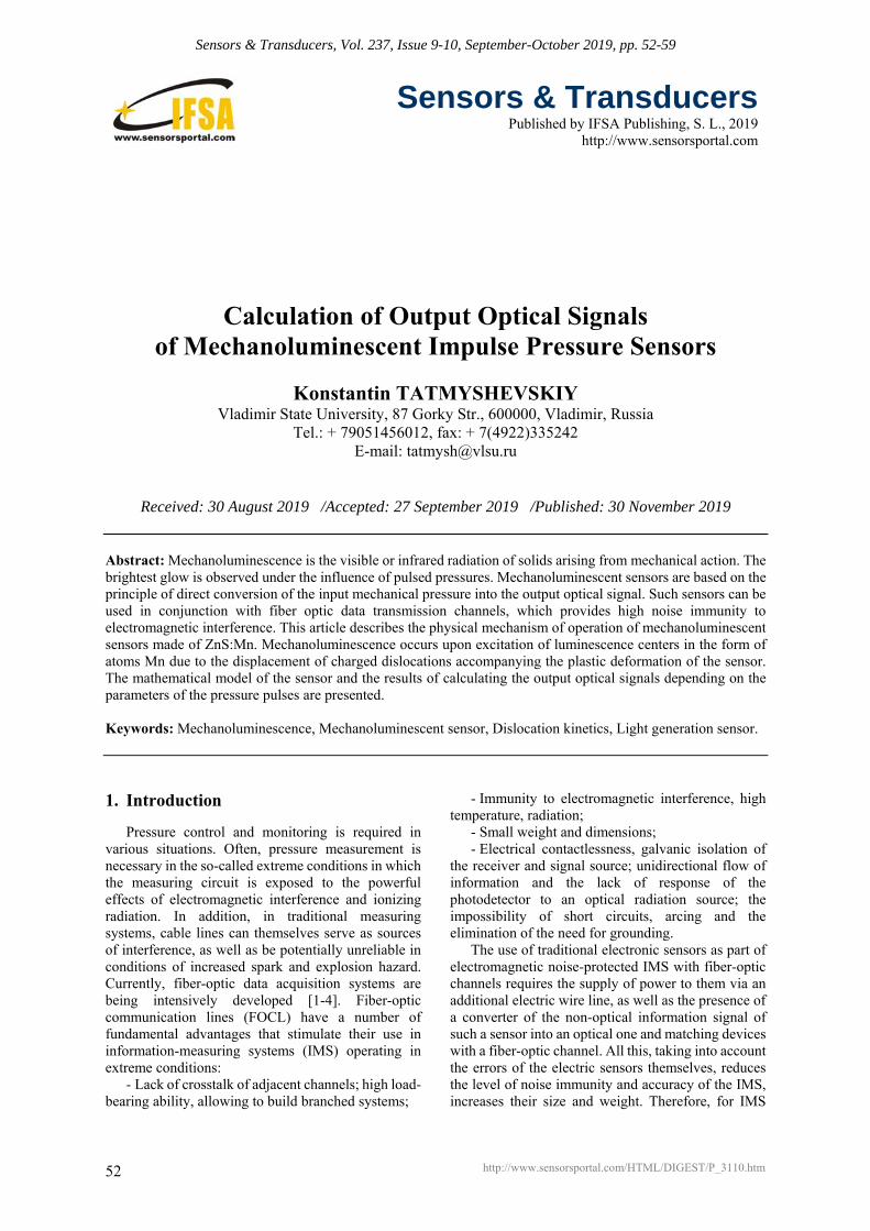
Sensors & Transducers, Vol. 237, Issue 9-10, September-October 2019, pp. 52-59
52
Sensors & Transducers
Published by IFSA Publishing, S. L., 2019 http://www.sensorsportal.com
Calculation of Output Optical Signals of Mechanoluminescent Impulse Pressure Sensors
Konstantin TATMYSHEVSKIY
Vladimir State University, 87 Gorky Str., 600000, Vladimir, Russia Tel.: + 79051456012, fax: + 7(4922)335242
E-mail: [email protected]
Received: 30 August 2019 /Accepted: 27 September 2019 /Published: 30 November 2019 Abstract: Mechanoluminescence is the visible or infrared radiation of solids arising from mechanical action. The brightest glow is observed under the influence of pulsed pressures. Mechanoluminescent sensors are based on the principle of direct conversion of the input mechanical pressure into the output optical signal. Such sensors can be used in conjunction with fiber optic data transmission channels, which provides high noise immunity to electromagnetic interference. This article describes the physical mechanism of operation of mechanoluminescent sensors made of ZnS:Mn. Mechanoluminescence occurs upon excitation of luminescence centers in the form of atoms Mn due to the displacement of charged dislocations accompanying the plastic deformation of the sensor. The mathematical model of the sensor and the results of calculating the output optical signals depending on the parameters of the pressure pulses are presented. Keywords: Mechanoluminescence, Mechanoluminescent sensor, Dislocation kinetics, Light generation sensor. 1. Introduction
Pressure control and monitoring is required in various situations. Often, pressure measurement is necessary in the so-called extreme conditions in which the measuring circuit is exposed to the powerful effects of electromagnetic interference and ionizing radiation. In addition, in traditional measuring systems, cable lines can themselves serve as sources of interference, as well as be potentially unreliable in conditions of increased spark and explosion hazard. Currently, fiber-optic data acquisition systems are being intensively developed [1-4]. Fiber-optic communication lines (FOCL) have a number of fundamental advantages that stimulate their use in information-measuring systems (IMS) operating in extreme conditions:
- Lack of crosstalk of adjacent channels; high load-bearing ability, allowing to build branched systems;
- Immunity to electromagnetic interference, high temperature, radiation;
- Small weight and dimensions; - Electrical contactlessness, galvanic isolation of
the receiver and signal source; unidirectional flow of information and the lack of response of the photodetector to an optical radiation source; the impossibility of short circuits, arcing and the elimination of the need for grounding.
The use of traditional electronic sensors as part of electromagnetic noise-protected IMS with fiber-optic channels requires the supply of power to them via an additional electric wire line, as well as the presence of a converter of the non-optical information signal of such a sensor into an optical one and matching devices with a fiber-optic channel. All this, taking into account the errors of the electric sensors themselves, reduces the level of noise immunity and accuracy of the IMS, increases their size and weight. Therefore, for IMS
http://www.sensorsportal.com/HTML/DIGEST/P_3110.htm

Sensors & Transducers, Vol. 237, Issue 9-10, September-October 2019, pp. 52-59
53
with fiber-optic communication channels, it is preferable to use parametric and generator sensors that use signals of the same physical nature in their work as optical fibers, that is, optical [1, 3-4].
Mechanoluminescent light-generating pressure sensors fully correspond to the fulfillment of the second condition. Here, the use of output light signals solves the problems of pairing sensors with FOCLs and increasing the noise immunity to electromagnetic interference, the absence of moving parts, the solidity and planarity of the sensing element provide reliability, and the use of its spatial modulation in addition to the amplitude-time parameters of the optical signal, various spectra and polarization states increases the information content.
Mechanoluminescent sensors (MLS) are based on the principle of direct conversion of the mechanical energy of an elastoplastic deformation into the energy of optical radiation, which is recorded by a photodetector [5]. Structurally, MLS is a thin-layer element, which includes fine crystalline phosphor powder (ZnS:Mn) and a transparent binding material. Mn atoms play the role of luminescence centers (LC) in these sensors [6-7]. The optimum thickness of the MLS does not exceed 20...100 µm, which is determined by the particle size distribution of the powder and the characteristics of light propagation in fine powder layers. Film MLS in conjunction with a matrix photodetector allows you to visualize and record impulse pressure fields [8].
Such sensors can be used, for example, to control the operation of automotive airbags, as sensors for structural damage, planar sensors for visualizing impulsed pressure fields [9-11].
2. Mechanoluminescent Sensor
2.1. Block Diagram of an Information Circuit with MLS
A generalized block diagram of the information
circuit of a measuring device with a MLS is shown in Fig. 1.
Fig. 1. Generalized block diagram of energy conversion in the information circuit of a recording device with MLS.
The scheme corresponds to the structure of a conventional optocoupler and includes a MLS, a photodetector, and an optical communication channel between them.
Here, the pressure (mechanical stress) σ(t) acts at the sensor input, causing deformation of the phosphor crystals. Under the action of deformation, the luminescent material is excited and generates a light pulse Φ(t). Since the radiating surface of the MLS has a fine-grained structure, and the phosphor crystals are opaque, only part of the total generated radiation energy will act at the output of the MLS. Depending on the ratio of the sizes of the luminous region and the input aperture of the optical medium, only part of the radiation Ф'(t) can be introduced into it. Losses within the optical medium are characterized by transmittance. At the exit from it and, accordingly, on the receiving surface of the photodetector, the light flux Ф''(t) will act. With the known sensitivity of the photodetector, the voltage at its output will be U(t), which is then amplified by a pre-normalizing (normalizing) amplifier to the value U'(t). Further, the signal can be fed to a processing unit or a computer, where it is subjected to analog-to-digital conversion and subsequent digital processing according to a predetermined algorithm.
The values of gain, photosensitivity, and transmittance (loss coefficient) of the optical medium, as a rule, are known for various components of the information circuit. Therefore, in order to calculate the output optical signals of the MLS, it is first necessary to determine: 1) how is the conversion of mechanical energy to radiation energy; 2) what parameters of the output optical signal are informative and how they are functionally related to the parameters of the input pressure pulse; 3) how efficiently the optical radiation is removed from the sensitive element to the optical communication channel. 2.2. MLS Design Requirements
The conversion coefficient of the optoelectronic circuit with MLS as the ratio of the voltage at the output of the photodetector to the input pressure at the input of the sensor is determined by the equation:
Kconv=Ф σ ηoutηOCCηinSλKAmp,
where Ф(σ) is the conversion function connecting the input pressure and the output light flux; ηout is the coefficient of radiation output from the surface of the MLS to the optical communication channel; ηOCC is the coefficient of radiation loss in the optical communication channel; ηin is the input coefficient of radiation from the optical communication channel to the photodetector; Sλ is the sensitivity of the photodetector in the band of the spectrum of ML radiation; KAmp is the amplifier gain.
To achieve high values Kconv, it is necessary to use highly efficient components. The requirements for the photodetector in terms of detection ability, sensitivity and fast action, and for the amplifier in terms of the slew rate of the output voltage and gain. It is necessary
Photodetector
U'(t)
Mechanoluminescent sensor
Photo detector
Optical communication channel
Open opt ical space /
optical fiber
σ(t) Ф'(t) Ф"(t) U(t)Ф(t)
Radiating surface
AmplifierConversionmechanism

Sensors & Transducers, Vol. 237, Issue 9-10, September-October 2019, pp. 52-59
54
to maximize the coupling of the emitter and the photodetector according to the spectral characteristics, and also to minimize radiation losses in the optical communication channel [1, 4].
The main prerequisites for the development of measuring devices with MLS is the knowledge of the conversion function Ф(σ) and the provision on the basis of this knowledge of high levels of radiation flux when exposed to a pressure sensor that is characteristic of the actual operating conditions of the product. Knowing the conversion function and the radiation spectrum makes it possible to most efficiently construct the photodetector scheme, as well as calculate the parameters of the MLS and other sensor elements. It should be noted that in contrast to photoluminescence and cathodoluminescence, mechanoluminescent properties characterize both the applied mechanoluminophore and the sensor design. This is due to the pulsed mechanical nature of the inlet pressure effect on the MLS. Therefore, the output radiation flux largely depends on whether it is possible in this hypothetical design to efficiently transfer mechanical energy to a sensitive element.
The basic requirements for the MLS design can be formulated as follows:
- The design must ensure the supply of energy of the pressure pulse to the MLS and the output of radiation from the surface of the MLS to the optical communication channel;
- The sensitive element should give out a radiation pulse with an amplitude and duration that ensure reliable recording in a given range of input actions;
- The output optical signal must have informative parameters (parameter), which allow unambiguous determination of the main parameters of the input pressure pulse σ(t).
Due to the fact that the MLS is actually an emitter with mechanical excitation, its main properties can be described by the characteristics and parameters used to describe the properties of emitters. 2.3. ML Sensor Structure
The optical parameters of a mechanoluminescent sensitive element that determine the radiation transfer in it, primarily depend on its structure. In the most common simplest case, the MLS structure is a plane-parallel light-scattering layer of particles of powdered luminescent material in a solidified transparent binder. Such a layer is applied to a substrate made of a transparent material, which ensures, firstly, the creation of the stress state of the particles during the propagation of a pressure impulse (a wave of mechanical stresses) through the layer, and secondly, the radiation is removed to a photodetector. Epoxy, melamine-formaldehyde and other resins, varnishes, polystyrene and other transparent materials are used as a binder for powder phosphors. Plates from various glasses, optical ceramics, fiber optic bundles and cables, foci can be used as a substrate.
Fig. 2 shows the structure MLS. The sensitive element of the sensor is a thin film of a hardened suspension of luminescent powder in a transparent binder.
Fig. 2. The structure of the sensitive element of the MLS: 1 - Pressure transmission element; 2 - Phosphor particles; 3 - Transparent binder material; 4 - Transparent substrate.
The optical parameters of the MLS, which determine the transfer of radiation in it, primarily depend on its internal structure. The most significant parameter of MLS is the thickness of the sensitive element. The thickness of the layer, the volume concentration of the powder particles in it, and the weight concentration of the dopant that creates the LC determine the total number of NLC participating in the radiation process. Conventionally, individual particles of the phosphor can be considered balls of the same diameter, uniformly located on the surface of the substrate and not overlapping each other. We call such a single-row layer of particles a monolayer. For a layer of n with such layers, the volume packing coefficient kV, which is equal to the ratio of the volumes of all particles to the volume of the layer, is limited to 0.86. Actually achieved values of kV usually lie in the range 0.3 ≤ kV ≤ 0.73.
The total flux of MLS radiation increases with an increase in the number of particles in a monolayer and with an increase in the number of monolayers, however, an increase in the flux reaches saturation, since with a sufficiently large number of monolayers the luminescence of deeply lying layers is completely scattered by the overlying layers. The transparency of a single monolayer can be taken equal to (1-kV). Thus, it is assumed that a single particle transmits only its radiation and is opaque to radiation from underlying particles, and the radiation passes only in the gaps between the particles. Denoting the radiation flux of the monolayer Φ1(t) closest to the substrate, we determine the total flux from the sensitive element with a thickness hse:
Ф t =Ф1 t 1+ ∑ 1-kVin
i=1 =Ф1 t kn, (1)
Ф1(t)
hse
1
4
3
2
σ(t)
dav
Ф(t)Ф1(1-kv)
n-1

Sensors & Transducers, Vol. 237, Issue 9-10, September-October 2019, pp. 52-59
55
where n = hse/dav - number of layers; dav is the average particle diameter of the phosphor; i is the number of layers except the first; kn is the coefficient of unevenness of the contribution of the glow of the layers. This equation makes it possible to bring the total radiation flux Ф(t) to the flux of the first monolayer Ф1(t), and to take into account the non-uniformity of the contribution of the remaining layers to the total flux using the luminance unevenness coefficient kn. An analysis of Eq. (1) shows that the optimal number of layers is n =3...6, since their further increase will give an increase in luminous flux of not more than 5 %.
A separate MLS monolayer emits a stream within the full solid angle. In this case, only half of the total flux comes out in the direction of the photodetector, the second half is scattered by the underlying layers and does not enter the photodetector, which is taken into account by the coefficient kΩ = 0.5.
The radiation losses that occur when the MLS radiation is introduced into the optical communication channel must be taken into account by the additional radiation input coefficient kin. Thus, taking into account the design parameters and the internal structure of the sensitive element, the total flux of radiation output from the site to the optical channel can be found as Ф(t) = 0.5 kin kn Ф1(t). 3. Mathematical Model 3.1. Mechanoluminescence Mechanism
It has been shown that mechanoluminescence
(ML) in crystalline compounds is a consequence of the processes of motion of dislocations that accompany the plastic deformation in crystals [12]. Dislocations in A2B6 semiconductors, and in particular ZnS, have a strong electrical charge. In the process of plastic deformation, LC interacts with the electric field of moving charged dislocations, which leads to the excitation of LC with their subsequent radiative transitions.
The physical model of ML is based on the phenomenon of tunneling of electrons in impurity LC in an electric field of moving dislocations arising from plastic deformation of a crystal [12]. During plastic deformation, the dislocations begin to move within the volume of the crystal. While the plastic deformation continues, excitation processes of LC prevail. After its termination, an exponential decrease in luminescence is observed due to the transition of excited LC to the stationary state.
3.2. Radiation Kinetics Equation
The specific flux of optical radiation in MLS is determined by the equation:
Ф t =η
τexp -
t
τNLC 2rin t NmD t VD t dt
tσ0
, (2)
where η is the energy of a light quantum; τ is the time constant corresponding to the exponential attenuation of the intracenter mechanoluminescent characteristic of Mn atoms; tσ is the pressure pulse duration time; NLC is the total number of LC in the sensor; rin(t) is the interaction radius of a moving dislocation with LC; NmD t is the average density of mobile dislocations; VD t is the average dislocation velocity. Here, the integrand describes the kinetics of excitation of LC during the action of the pressure pulse tσ, and the equation before the integral describes the kinetics of luminescence attenuation. 3.3. Sensor Deformation Equation
The kinetics of excitation depends on plastic strain εp, the speed of which is determined by the Orowan equation [13]:
where b is the modulus of the Burgers vector characterizing the lattice distortion by the dislocation. The stress-strain state of MLS for the case of uniaxial application of pressure is determined by the equation:
σ1=E ε1-4
3εp =σ t -Eε1p, (4)
where σ1 is the principal stress applied perpendicular to the MLS plane, E is the Young’s modulus, ε1 is the total strain in the form of the sum of the elastic ε1e and plastic ε1p components, σ(t) is the pressure pulse. Eq. (4) shows that stresses increase with an increase in total strain ε1, and decrease due to plastic ε1p. Here the case of quasistatic deformation, i.e. observance of uniformity of plastic deformations across the thickness of the MLS was considered. This condition is fulfilled either at low strain rates or at small ratios of the thickness of the sensor to its diameter.
Dislocation parameters are found by Gilman equations [14]
NmD=NtDexp − NtDNtcr
, (5)
NtD=NtD0+Mεp, (6)
where NtD is the average total dislocation density; Ntcr is the critical value of the total dislocation density corresponding to the end of the yield area in the σ(ε) diagram, NtD0 is the initial value of the total density of dislocations; M is the dislocation multiplication factor.
The average dislocation velocity can be determined by the Eq. [14]:
εp = b NmD t VD t , (3)

Sensors & Transducers, Vol. 237, Issue 9-10, September-October 2019, pp. 52-59
56
VD t =ksctrexpDf
σ1, (7)
where
ks = 0, if σ1<σS;
1-2exp 0,5 σS-σ1
σ1-σS
, if σ1>σS,
ks is the correction factor, zeroing the speed of dislocations at pressures below the yield strength; ctr is the shear wave velocity in the crystal; Df is the effective stress of internal friction; σS is the static yield strength. The average velocity of dislocations in the Eq. (3) is very sensitive to shear stresses in the slip plane and in the limit can reach values of ctr. However, in the region close to the limit of static yield stress, the Eq. (7) must be corrected, since it does not take into account the existence of a threshold value of the yield stress below which dislocation motion does not occur. This threshold value is determined by the existence of the so-called Peierls-Nabarro barrier [15] and is associated with a static yield strength σS. Therefore, in the region of low stresses σ1<σS, the correction coefficient ks is introduced into dependence (7), which does not change VD if σ1<σS and decreases VD at σ1>σS. 3.4. Settlement Conditions
Modeling of the light flux arising when a mechanoluminescent sensing element is excited by a pressure pulse is performed in MATLAB. The program determines the quantum-mechanical, electrical and kinetic characteristics of the mechanoluminescent material based on the industrial electroluminophore ELS-580C.
The mathematical model is a system of integro-differential Equations (2) and (3). The ode113 function was chosen from the MATLAB function library to solve the ordinary differential equation. Is a solver of variable order based on the formula of Adams - Bashforth - Moulton. It can be more effective than the usual Runge-Kutta method of the 4th and 5th order at high requirements to accuracy and in cases when the complexity of calculating the right parts is high. It is a multi-step solver that requires knowing the solutions at several preceding points to compute the solution at the current point.
To calculate a certain integral, the Quadra-tour - quad method was chosen. Quadrature is a numerical method for calculating the area under a function graph. The function quad ('fun', a, b) returns the numerical value of a certain integral from a given function ' fun ' on the segment [a b]. The adaptive Simpson method is used.
ELS-580C industrial electroluminophore (composition - ZnS:Mn, Cu; weight-percent manganese content of 1 %) was chosen as the mechanoluminescent material in the calculations. The
reasons for choosing this particular material for theoretical and experimental studies were as follows:
- Zinc sulfide phosphors activated by manganese have the brightest luminescence under mechanical stress;
- The maximum of the emission spectrum corresponds to the yellow-orange glow and is more consistent with the maximum spectral sensitivity of modern high-speed silicon photodetectors;
- This electroluminophore is produced by the industry in series. Therefore, its physical, chemical and mechanical properties are quite reproducible and a priori known.
The latter circumstance can be recognized as very important, since the results of numerous studies [4-5, 8-11, 16] show contradictory results, which are not only inconsistent with each other, but also differ within the framework of one experimental study [7]. One explanation for such discrepancies may be the fact that the researchers did not control both the actual dislocation structure of crystalline samples and the history of their mechanical loading. Analysis of Eqs. (5) and (6) shows that the initial dislocation density NtD0 and its relation to the critical density Ntcr have a very strong effect on the density of mobile dislocations NmD, which largely determines the intensity of mechanoluminescent radiation.
To determine the magnitude of the Burgers vector, an assumption was made that the material is a single sphalerite structure. In the calculations, only the energy of radiation quanta corresponding to the maximum of the emission spectrum of manganese emission centers (λ=580 nm; η=3.52 10-19 J) was taken into account, since the radiation intensity of copper LCs is approximately 50 times weaker [17-19].
The parameters of the dislocation structure of the phosphor were determined taking into account the production technology of luminescent powders. In the performed calculations, the values kin=1, n=2, dav=10 μm, kV=0.6, and kn=1.4 were taken. These values were chosen because they corresponded to the fabricated experimental MLS samples.
The luminescence decay kinetics corresponds to intracenter luminescence [18], characteristic of ZnS: Mn, with a time constant τ = 150 μs. The energy luminosity of the MLS R(t)=0.5kinknФ1(t) was calculated, i.e., the flow power emitted by a unit surface area equal to 1 mm2 was calculated.
3.5. Key Model Assumptions
When constructing a mathematical model of a mechanoluminescent sensing element, the following basic assumptions were made:
1) Only one type of luminescence centers (Mn) are involved in the formation of radiation, which generate light quanta with a fixed energy;
2) The probability of tunneling is equal to one; 3) The centers of luminescence are evenly
distributed inside the crystal;
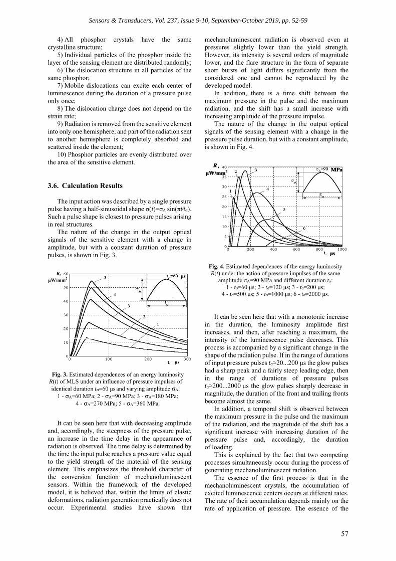
Sensors & Transducers, Vol. 237, Issue 9-10, September-October 2019, pp. 52-59
57
4) All phosphor crystals have the same crystalline structure;
5) Individual particles of the phosphor inside the layer of the sensing element are distributed randomly;
6) The dislocation structure in all particles of the same phosphor;
7) Mobile dislocations can excite each center of luminescence during the duration of a pressure pulse only once;
8) The dislocation charge does not depend on the strain rate;
9) Radiation is removed from the sensitive element into only one hemisphere, and part of the radiation sent to another hemisphere is completely absorbed and scattered inside the element;
10) Phosphor particles are evenly distributed over the area of the sensitive element.
3.6. Calculation Results The input action was described by a single pressure
pulse having a half-sinusoidal shape σ(t)=σA sin(πt⁄tσ). Such a pulse shape is closest to pressure pulses arising in real structures.
The nature of the change in the output optical signals of the sensitive element with a change in amplitude, but with a constant duration of pressure pulses, is shown in Fig. 3.
Fig. 3. Estimated dependences of an energy luminosity R(t) of MLS under an influence of pressure impulses of identical duration tσ=60 μs and varying amplitude σА:
1 - σА=60 MPa; 2 - σА=90 MPa; 3 - σА=180 MPa; 4 - σА=270 MPa; 5 - σА=360 MPa.
It can be seen here that with decreasing amplitude and, accordingly, the steepness of the pressure pulse, an increase in the time delay in the appearance of radiation is observed. The time delay is determined by the time the input pulse reaches a pressure value equal to the yield strength of the material of the sensing element. This emphasizes the threshold character of the conversion function of mechanoluminescent sensors. Within the framework of the developed model, it is believed that, within the limits of elastic deformations, radiation generation practically does not occur. Experimental studies have shown that
mechanoluminescent radiation is observed even at pressures slightly lower than the yield strength. However, its intensity is several orders of magnitude lower, and the flare structure in the form of separate short bursts of light differs significantly from the considered one and cannot be reproduced by the developed model.
In addition, there is a time shift between the maximum pressure in the pulse and the maximum radiation, and the shift has a small increase with increasing amplitude of the pressure impulse.
The nature of the change in the output optical signals of the sensing element with a change in the pressure pulse duration, but with a constant amplitude, is shown in Fig. 4.
Fig. 4. Estimated dependences of the energy luminosity R(t) under the action of pressure impulses of the same
amplitude σA=90 MPa and different duration tσ: 1 - tσ=60 μs; 2 - tσ=120 μs; 3 - tσ=200 μs;
4 - tσ=500 μs; 5 - tσ=1000 μs; 6 - tσ=2000 μs.
It can be seen here that with a monotonic increase in the duration, the luminosity amplitude first increases, and then, after reaching a maximum, the intensity of the luminescence pulse decreases. This process is accompanied by a significant change in the shape of the radiation pulse. If in the range of durations of input pressure pulses tσ≈20...200 μs the glow pulses had a sharp peak and a fairly steep leading edge, then in the range of durations of pressure pulses tσ≈200...2000 μs the glow pulses sharply decrease in magnitude, the duration of the front and trailing fronts become almost the same.
In addition, a temporal shift is observed between the maximum pressure in the pulse and the maximum of the radiation, and the magnitude of the shift has a significant increase with increasing duration of the pressure pulse and, accordingly, the duration of loading.
This is explained by the fact that two competing processes simultaneously occur during the process of generating mechanoluminescent radiation.
The essence of the first process is that in the mechanoluminescent crystals, the accumulation of excited luminescence centers occurs at different rates. The rate of their accumulation depends mainly on the rate of application of pressure. The essence of the
μs
μsμW/mm2
R,

Sensors & Transducers, Vol. 237, Issue 9-10, September-October 2019, pp. 52-59
58
second process is the return of the excited glow centers to the initial state, which is accompanied by the emission of light quanta (luminescence). The second process has a constant speed, which is described by the law of the mono-molecular reaction (exponential attenuation).
Accordingly, if the excitation rate is much higher than the return velocity, then intense mechanoluminescence with a steep rise front will be observed. In the opposite case, the concentration of excited centers of luminescence will not be enough for noticeable radiation to appear. Such a process will occur even despite the fact that the total deformation of the phosphor of the sensing element can be significantly greater than at high loading speeds. This manifests itself repeatedly noted by various researchers, a significant sensitivity of the intensity of mechanoluminescence to the speed of mechanical loading.
4. Conclusions
A mathematical model of MLS based on zinc sulfide phosphor doped with manganese has been developed. The model is based on a clear interpretation of the physical processes leading to mechanoluminescence. The developed methodology for calculating the output optical signals of the MLS allows us to determine the magnitude of the signal in absolute units of light flux. The model takes into account the design features of the MLS. The results are in good agreement with experimental data [20].
The calculation results show that, firstly, the MLS conversion function has a pronounced sensitivity threshold, secondly, the conversion function has a substantially nonlinear character, and thirdly, the shape of the output optical signals differs significantly from the shape of the input pressure pulses.
Comparison of the obtained results with the data of modern semiconductor photodetectors showed that reliable detection of the optical MLS signal is possible for further processing. The results were presented briefly at the conference [21].
References [1]. E. Udd (Editor), Fiber Optic Sensors: An Introduction
for Engineers and Scientists, 2nd Edition, Wiley-Interscience, New York, NY, 2006.
[2]. J. Fraden, Handbook of Modern Sensors: Physics, Designs and Applications, 5th Edition, Springer, New York, 2016.
[3]. R. J. Jackson, Novel Sensors and Sensing, CRC Press, Boca Raton, 2004.
[4]. D. O. Olawale, T. Dickens, W. G. Sullivan, O. I. Okoli, J. O. Sobanjo, B. Wang, Progress in triboluminescence-based smart optical sensor system, Journal of Luminescence, Vol. 131, Issue 7, 2011, pp. 1407-1418.
[5]. B. P. Chandra, «Mechanoluminescence», in Luminescence of Solids, Editer by D. R. Vij, Plenum Press, New York, 1998, pp. 361-389.
[6]. L. Kobakhidze, C. J. Guidry, W. A. Hollerman, R. S. Fontenot, Detecting Mechanoluminescence from ZnS:Mn Powder Using a High Speed Camera, IEEE Sensors Journal, Vol. 13, Issue 8, 2013, pp. 3053-3059.
[7]. Chao-Nan Xu, Xu-Guang Zheng, Tadahiko Watanabe, Morio Akiyama, Ichiro Usui, Enhancement of adhesion and triboluminescence of ZnS:Mn films by annealing technique, Thin Solid Films, Vol. 352, Issue 1-2, 1999, pp. 273-277.
[8]. V. K. Chandra, B. P. Chandra, Dynamics of the mechanoluminescence induced by elastic deformation of persistent luminescent crystals, Journal of Luminescence, Vol. 132, Issue 3, 2012, pp. 858-869.
[9]. I. Sage, G. Bourhill, Triboluminescent materials for structural damage monitoring, Journal of Materials Chemistry, Vol. 11, Issue 2, 2001, pp. 231-245.
[10]. N. P. Bergeron, W. A. Hollerman, S. M. Goedeke, M. Hovater, W. Hubbs, A. Finchum, R. J. Moore, S. W. Allison, D. L. Edwards, Experimental evidence of triboluminescence induced by hypervelocity impact, International Journal of Impact Engineering, Vol. 33, Issue 1-12, 2006, pp. 91-99.
[11]. A. Feng, S. Michels, A. Lamberti, P. F. Smet, Mechanoluminescent materials: a new way to analyze stress by light, in Proceedings of the 18th International Conference on Experimental Mechanics (ICEM’18), Brussels, Belgium, 1–5 July 2018, Vol. 2, Issue 8, 492.
[12]. Yu A. Ossipian, et al., Electronic properties of dislocations in semiconductors, Editorial USSR, Moscow, 2000.
[13]. J. W. Taylor, Dislocation dynamics and dynamic yielding, Journal of Applied Physics, Vol. 36, Issue 10, 1965, pp. 3146-3150.
[14]. J. J. Gilman, Dislocation dynamics and response of materials to impact, Applied Mechanics Reviews, Vol. 21, Issue 8, 1968, pp. 767-783.
[15]. J. P. Hirth, J. Lothe, Theory of Dislocations, Wiley-Interscience Publication, Toronto, 2nd Edition, 1982.
[16]. W. A. Hollerman, R. S. Fontenot, K. N. Bhat, M. D. Aggarwal, C. J. Guidry, K. M. Nguyen, Comparison of triboluminescent emission yields for 27 luminescent materials, Optical Materials, Vol. 9, 2012, pp. 1521-1547.
[17]. P. Thiessen, K. Meyer, Triboluminescenz bei Verformungs fester Körper, Naturwissenschaften, Vol. 9, 1970, pp. 423-427.
[18]. L. Sodomka, Mechanoluminiscence a jeji pouziti, Academia, Praha, 1985, 226 p.
[19]. B. P. Chandra, M. S. Khan, M. H. Ansari, Cleavage Mechanoluminescence in Crystals, Crystal Research and Technology, Vol. 33, Issue 2, 1998, pp. 291-302.
[20]. N. Yu. Makarova, K. V. Tatmyshevskiy, A table for experimental study of mechanoluminescent pulse pressure transducers, Instruments and Experimental Techniques, Vol. 49, Issue 1, 2006, pp. 135-140.
[21]. K. Tatmyshevskiy, Mechanoluminescent pulse pressure sensors, in Proceedings of the 5th International Conference on Sensors Engineering and Electronics Instrumentation Advances (SEIA'19), Tenerife (Canary Islands), Spain, 25-27 September 2019, pp. 182-184.

Sensors & Transducers, Vol. 237, Issue 9-10, September-October 2019, pp. 52-59
59
__________________
Published by International Frequency Sensor Association (IFSA) Publishing, S. L., 2019 (http://www.sensorsportal.com).
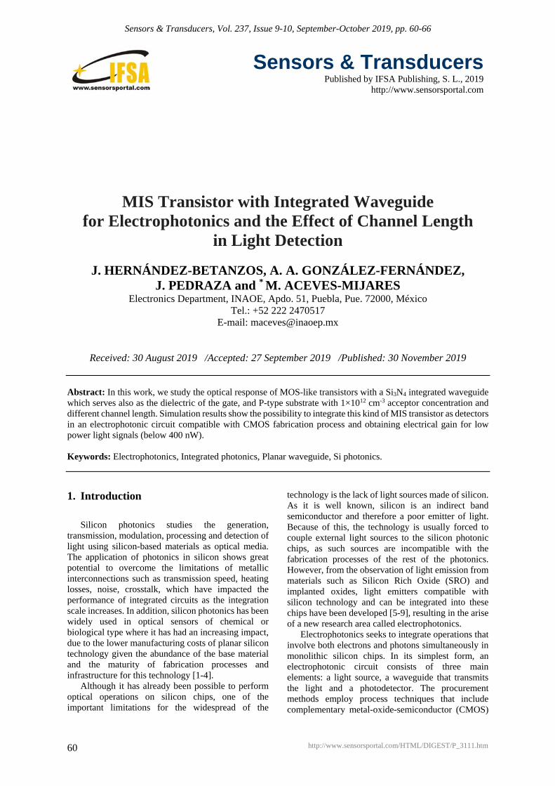
Sensors & Transducers, Vol. 237, Issue 9-10, September-October 2019, pp. 60-66
60
Sensors & Transducers
Published by IFSA Publishing, S. L., 2019 http://www.sensorsportal.com
MIS Transistor with Integrated Waveguide for Electrophotonics and the Effect of Channel Length
in Light Detection
J. HERNÁNDEZ-BETANZOS, A. A. GONZÁLEZ-FERNÁNDEZ, J. PEDRAZA and * M. ACEVES-MIJARES
Electronics Department, INAOE, Apdo. 51, Puebla, Pue. 72000, México Tel.: +52 222 2470517
E-mail: [email protected]
Received: 30 August 2019 /Accepted: 27 September 2019 /Published: 30 November 2019 Abstract: In this work, we study the optical response of MOS-like transistors with a Si3N4 integrated waveguide which serves also as the dielectric of the gate, and P-type substrate with 1×1012 cm-3 acceptor concentration and different channel length. Simulation results show the possibility to integrate this kind of MIS transistor as detectors in an electrophotonic circuit compatible with CMOS fabrication process and obtaining electrical gain for low power light signals (below 400 nW). Keywords: Electrophotonics, Integrated photonics, Planar waveguide, Si photonics.
1. Introduction Silicon photonics studies the generation,
transmission, modulation, processing and detection of light using silicon-based materials as optical media. The application of photonics in silicon shows great potential to overcome the limitations of metallic interconnections such as transmission speed, heating losses, noise, crosstalk, which have impacted the performance of integrated circuits as the integration scale increases. In addition, silicon photonics has been widely used in optical sensors of chemical or biological type where it has had an increasing impact, due to the lower manufacturing costs of planar silicon technology given the abundance of the base material and the maturity of fabrication processes and infrastructure for this technology [1-4].
Although it has already been possible to perform optical operations on silicon chips, one of the important limitations for the widespread of the
technology is the lack of light sources made of silicon. As it is well known, silicon is an indirect band semiconductor and therefore a poor emitter of light. Because of this, the technology is usually forced to couple external light sources to the silicon photonic chips, as such sources are incompatible with the fabrication processes of the rest of the photonics. However, from the observation of light emission from materials such as Silicon Rich Oxide (SRO) and implanted oxides, light emitters compatible with silicon technology and can be integrated into these chips have been developed [5-9], resulting in the arise of a new research area called electrophotonics.
Electrophotonics seeks to integrate operations that involve both electrons and photons simultaneously in monolithic silicon chips. In its simplest form, an electrophotonic circuit consists of three main elements: a light source, a waveguide that transmits the light and a photodetector. The procurement methods employ process techniques that include complementary metal-oxide-semiconductor (CMOS)
http://www.sensorsportal.com/HTML/DIGEST/P_3111.htm
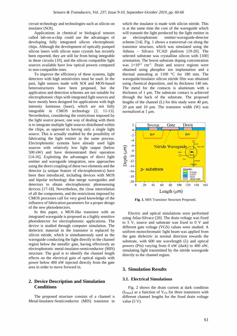
Sensors & Transducers, Vol. 237, Issue 9-10, September-October 2019, pp. 60-66
61
circuit technology and technologies such as silicon on insulator (SOI).
Applications in chemical or biological sensors called lab-on-a-chip could use the advantages of developing fully integrated silicon electrophonic chips. Although the development of optically pumped silicon lasers with silicon nano crystals has recently been reported, they are still far from being integrable in these circuits [10], and the silicon compatible light sources available have low optical powers compared to non-compatible ones.
To improve the efficiency of these systems, light detectors with high sensitivities must be used. In the past, light sensors made with SOI and MOS-based heterostructures have been proposed, but the application and detection schemes are not suitable for electrophotonic chips with integrated light sources and have mostly been designed for applications with high intensity luminous (laser), which are not fully integrable in CMOS technology [2, 11-13]. Nevertheless, considering the restrictions imposed by the light source power, one way of dealing with them is to integrate multiple light sources distributed within the chips, as opposed to having only a single light source. This is actually enabled by the possibility of fabricating the light emitter in the same process. Electrophotonic systems have already used light sources with relatively low light output (below 500 nW) and have demonstrated their operation [14-16]. Exploiting the advantages of direct light emitter and waveguide integration, new approaches using the direct coupling of these two elements and the detector (a unique feature of electrophotonics) have been then introduced, including devices with MOS and bipolar technology that merge waveguides and detectors to obtain electrophotonic photosensing devices [17-18]. Nevertheless, the close interrelation of all the components, and the restrictions imposed by CMOS processes call for very good knowledge of the influence of fabrication parameters for a proper design of the new photodetectors.
In this paper, a MOS-like transistor with an integrated waveguide is proposed as a highly sensitive photodetector for electrophotonic applications. The device is studied through computer simulation. The dielectric material in the transistor is replaced by silicon nitride, which is simultaneously used as the waveguide conducting the light directly to the channel region below the metallic gate, having effectively an electrophotonic metal-insulator-semiconductor (MIS) structure. The goal is to identify the channel length effects on the electrical gain of optical signals with power below 400 nW injected directly from the gate area in order to move forward in.
2. Device Description and Simulation Conditions The proposed structure consists of a channel n
Metal-Insulator-Semiconductor (MIS) transistor in
which the insulator is made with silicon nitride. This is at the same time the core of the waveguide which will transmit the light produced by the light emitter in an electrophotonic emitter-waveguide-detector scheme [14]. Fig. 1 shows a transversal cut along the transistor structure, which was simulated using the Athena – Silvaco TCAD platform [19-20]. The selected substrate was crystalline silicon with [100] orientation. The boron substrate doping concentration was 1×1012 cm-3. Drain and source regions were obtained using phosphor ion implantation and a thermal annealing at 1100 °C for 180 min. The waveguide/insulator silicon nitride film was obtained using chemical deposition, and its thickness 140 nm. The metal for the contacts is aluminum with a thickness of 1 µm. The substrate contact is achieved through the back of the substrate. The proposed lengths of the channel (L) for this study were 40 μm, 20 μm and 10 μm. The transistor width (W) was normalized at 1 µm.
Fig. 1. MIS Transistor Structure Proposed.
Electric and optical simulations were performed using Atlas-Silvaco [20]. The drain voltage was fixed to 5 V, source and substrate was fixed to 0 V and different gate voltage (VGS) values were studied. A uniform monochromatic light beam was applied from the gate dielectric in normal direction towards the substrate, with 600 nm wavelength (λ) and optical powers (Pin) varying from 0 nW (dark) to 400 nW, simulating light transmitted by the nitride waveguide directly to the channel region. 3. Simulation Results 3.1. Electrical Simulations
Fig. 2 shows the drain current at dark condition (IDdark) as a function of VGS for three transistors with different channel lengths for the fixed drain voltage value (5 V).

Sensors & Transducers, Vol. 237, Issue 9-10, September-October 2019, pp. 60-66
62
-2 -1 0 1 2
0
4µ
8µ
12µ
16µ
20µ
24µ
-2 -1 0 1 2
100p
1n
10n
100n
1µ
10µ
Dra
in C
urre
nt (
A)
Gate Voltage (V)
Dra
in C
urre
nt (
A)
Gate Voltage (V)
L=40 μm L=20 μm L=10 μm
VDS
=5V
Fig. 2. Drain Current of MIS transistor at dark condition. Threshold voltage is negative below Vgs=-0.36 V. IDdark tends to increase when the channel length is reduced.
The curves have the characteristic quadratic behavior. The threshold voltages for these transistors has negative values. This means that they operate in depletion mode, for 0 V in the gate, the transistor is turned on (a channel is formed). Threshold voltages are around to -0.36 V.
It is observed that the dark drain current (leakage current) increases when the channel length is decreased for the applied drain voltage. There is a difference of three orders of magnitude between the longest transistor and the shortest one. This means that the transistor with 10 µm channel length requires a higher gate voltage to be turned off. This leakage current could be decreased using lower drain voltages.
3.2. Optical Simulations
Fig. 3 shows the drain current under different illumination conditions for the transistor with 40 μm channel length. The value of λ= 600 nm was selected according to the emission spectra of previously reported SRO-based light sources embedded into nitride waveguides [14].
The presence of light increases the drain current values in whole gate voltage range. This means that the drain photo detection is independent of the gate bias condition, but the amount of photocurrent could depend on the gate bias value. The current value difference between dark condition and 80 nW illumination is approximately 400 times when the transistor is turned off.
In order to show only the drain current contribution due to the optical power, the dark current was subtracted from the total drain current ID. The optical drain current is:
Dopt D DdarkI I I= − , (1)
where ID is the total drain current and IDdark the drain current in dark condition.
-2 -1 0 1 2
100p
1n
10n
100n
1µ
10µ
Dra
in C
urre
nt (
A)
Gate Voltage (V)
Dark 80 nW 160 nW 240 nW 320 nW 400 nW
VDS
=5V
Fig. 3. Drain current under illumination. L is 40 μm. λ is 600 nm and drain voltage is 5 V. The presence of light
increases the drain current values.
Fig. 4 shows IDopt for different gate voltages and different light power stimulations (from 80 nW to 400 nW) for the MIS transistor with 40 µm channel length.
-2 -1 0 1 2
40n
80n
120n
160n
200n
240n
280n
320n
360n
400n
λ=600 nmL=40 μm VDS=5V
I Dop
t (A
)
Gate Voltage (V)
80 nW 160 nW 240 nW 320 nW 400 nW
Fig. 4. Optical drain current as a function of gate voltage. L is 40 μm. λ is 600 nm and drain voltage is 5 V. Optical drain current is generated in whole gate voltage range.
It is observed that the optical drain current has a modulation effect dependant on the gate voltage. The optical drain current is increased when the gate voltage is biased towards higher voltages for the same light power value, until reaching a maximum value and then decresing again, although always to higher values as compared to Vgs<-0.5 V biasing of the gate.
Fig. 5 shows the optical drain current for different gate voltages and different light power for the MIS transistor with 20 µm channel length.
In this case, the optical drain current varies between 200 nA and 900 nA for the range of applied optical powers, which is lower than the variation

Sensors & Transducers, Vol. 237, Issue 9-10, September-October 2019, pp. 60-66
63
registered for L=40 μm, in which the change was of one order of magnitude. The optical drain current has its maximum photo detection values around Vgs=-0.5 V and is decreased when the gate voltage moves away from this voltage to larger values.
-2 -1 0 1 2
200.0n
300.0n
400.0n
500.0n
600.0n
700.0n
800.0n
900.0n
λ=600 nmL=20 μm VDS=5V
I Dop
t(A)
Gate Voltage (V)
80 nW 160 nW 240 nW 320 nW 400 nW
Fig. 5. Optical drain current as a gate voltage function. L is 20 μm. λ is 600 nm and drain voltage is 5 V.
Finally, Fig. 6 shows the optical drain current for different gate voltages and different light power for the transistor with L=10 µm.
-2 -1 0 1 2
400.0n
800.0n
1.2µ
1.6µ
2.0µ
2.4µ
2.8µ
λ=600 nmL=10 μm VDS=5V
I Dop
t (A
)
Gate Voltage (V)
80 nW 160 nW 240 nW 320 nW 400 nW
Fig. 6. Optical drain current as a gate voltage function. L is 10 μm. λ is 600 nm and drain voltage is 5 V.
Here, it can also be observer an optical drain current increment for higher light power values, with larger changes in IDopt for values of Vgs < -1 V, value after which a saturation behavior is observed. For Vgs=-2 V, the optical drain current varied from 1.1 µA to 2.8 µA when the light power is varied from 80 nW to 400 nW. This particular case could be the better if the lowest posible dark current and major photodetection is desired.
4. Analysis and Discussion When the light is absorbed in the silicon substrate,
each absorbed photon could produce an electron-hole pair which under proper conditions can contribute to the generation of an excess current, called photocurrent. This current is maximum when each photon incident produces an electron-hole pair that contribute to the photocurrent, i.e., they do not recombine. The maximum available photocurrent provided by the light emitter Iph is a measure of the incident photons expressed as a current and is defined as [20]:
inph
PI q
hc
λ= , (2)
where q is the electron charge, h is the Planck Constant and c is the speed of light. For Pin = 80 nW and λ = 600 nm, Iph is 38.68 nA. This is the value of photogenerated current in ideal conditions (solely due to the incidence of photons and further generation of electron-hole pairs). If we compare this value with the simulated IDopt, it is possible to have an idea of the proportion of incident photons contributing to the generation of a detectable current. Fig. 7 shows the optical drain current for the different transistors and the ideal photocurrent Iph for 80 nW light power.
-2 -1 0 1 2
100n
1µ
I Dop
t (A
)
Gate Voltage (V)
Iph
(80 nW)
L= 40 μm L= 20 μm L= 10 μm
VDS
= 5Vλ= 600 nm
Fig. 7. Optical drain current as a gate voltage function. Pin is 80 nW, L is 40 μm. λ is 600 nm and drain voltage
is 5 V. IDopt is above Iph.
The photo generated drain current is greater than the Iph value and is increased when the channel length is decreased. This means the detection of a current whose value is higher than the maximum available from photo-generated electron-hole pairs, i. e., the existence of an optical photocurrent gain. To better analyze this, a photocurrent ratio between optical drain current IDopt and the ideal photocurrent Iph can be calculated and expressed as:
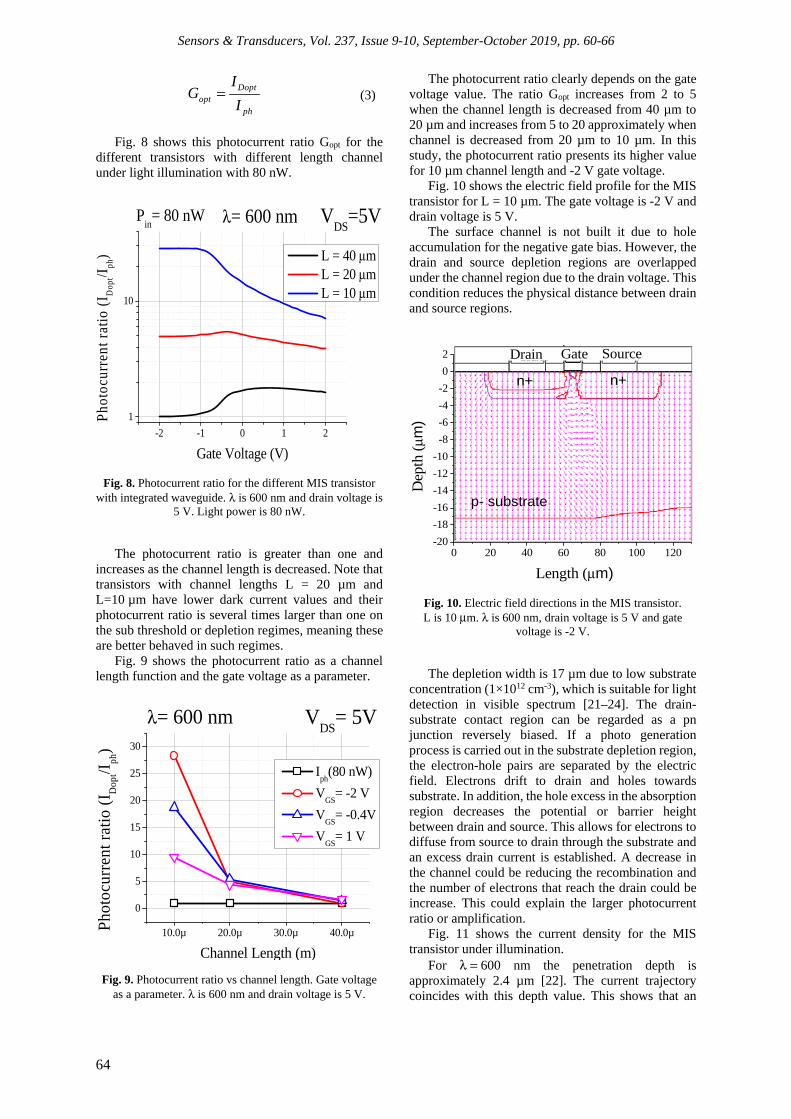
Sensors & Transducers, Vol. 237, Issue 9-10, September-October 2019, pp. 60-66
64
Doptopt
ph
IG
I= (3)
Fig. 8 shows this photocurrent ratio Gopt for the
different transistors with different length channel under light illumination with 80 nW.
-2 -1 0 1 2
1
10
Pho
tocu
rren
t rat
io (
I Dop
t/Iph
)
Gate Voltage (V)
L = 40 μm L = 20 μm L = 10 μm
VDS
=5VPin= 80 nW λ= 600 nm
Fig. 8. Photocurrent ratio for the different MIS transistor with integrated waveguide. λ is 600 nm and drain voltage is
5 V. Light power is 80 nW.
The photocurrent ratio is greater than one and increases as the channel length is decreased. Note that transistors with channel lengths L = 20 µm and L=10 µm have lower dark current values and their photocurrent ratio is several times larger than one on the sub threshold or depletion regimes, meaning these are better behaved in such regimes.
Fig. 9 shows the photocurrent ratio as a channel length function and the gate voltage as a parameter.
10.0µ 20.0µ 30.0µ 40.0µ
0
5
10
15
20
25
30
Phot
ocur
rent
rat
io (
I Dop
t/Iph
)
Channel Length (m)
Iph
(80 nW)
VGS
= -2 V
VGS
= -0.4V
VGS
= 1 V
VDS
= 5Vλ= 600 nm
Fig. 9. Photocurrent ratio vs channel length. Gate voltage as a parameter. λ is 600 nm and drain voltage is 5 V.
The photocurrent ratio clearly depends on the gate voltage value. The ratio Gopt increases from 2 to 5 when the channel length is decreased from 40 µm to 20 µm and increases from 5 to 20 approximately when channel is decreased from 20 µm to 10 µm. In this study, the photocurrent ratio presents its higher value for 10 µm channel length and -2 V gate voltage.
Fig. 10 shows the electric field profile for the MIS transistor for L = 10 µm. The gate voltage is -2 V and drain voltage is 5 V.
The surface channel is not built it due to hole accumulation for the negative gate bias. However, the drain and source depletion regions are overlapped under the channel region due to the drain voltage. This condition reduces the physical distance between drain and source regions.
0 20 40 60 80 100 120-20
-18
-16
-14
-12
-10
-8
-6
-4
-2
0
2
n+
SourceSource
Dep
th (
μm)
Length (μm)
SourceGateDrain
p- substrate
n+
Fig. 10. Electric field directions in the MIS transistor. L is 10 μm. λ is 600 nm, drain voltage is 5 V and gate
voltage is -2 V.
The depletion width is 17 µm due to low substrate concentration (1×1012 cm-3), which is suitable for light detection in visible spectrum [21–24]. The drain-substrate contact region can be regarded as a pn junction reversely biased. If a photo generation process is carried out in the substrate depletion region, the electron-hole pairs are separated by the electric field. Electrons drift to drain and holes towards substrate. In addition, the hole excess in the absorption region decreases the potential or barrier height between drain and source. This allows for electrons to diffuse from source to drain through the substrate and an excess drain current is established. A decrease in the channel could be reducing the recombination and the number of electrons that reach the drain could be increase. This could explain the larger photocurrent ratio or amplification.
Fig. 11 shows the current density for the MIS transistor under illumination.
For λ = 600 nm the penetration depth is approximately 2.4 µm [22]. The current trajectory coincides with this depth value. This shows that an
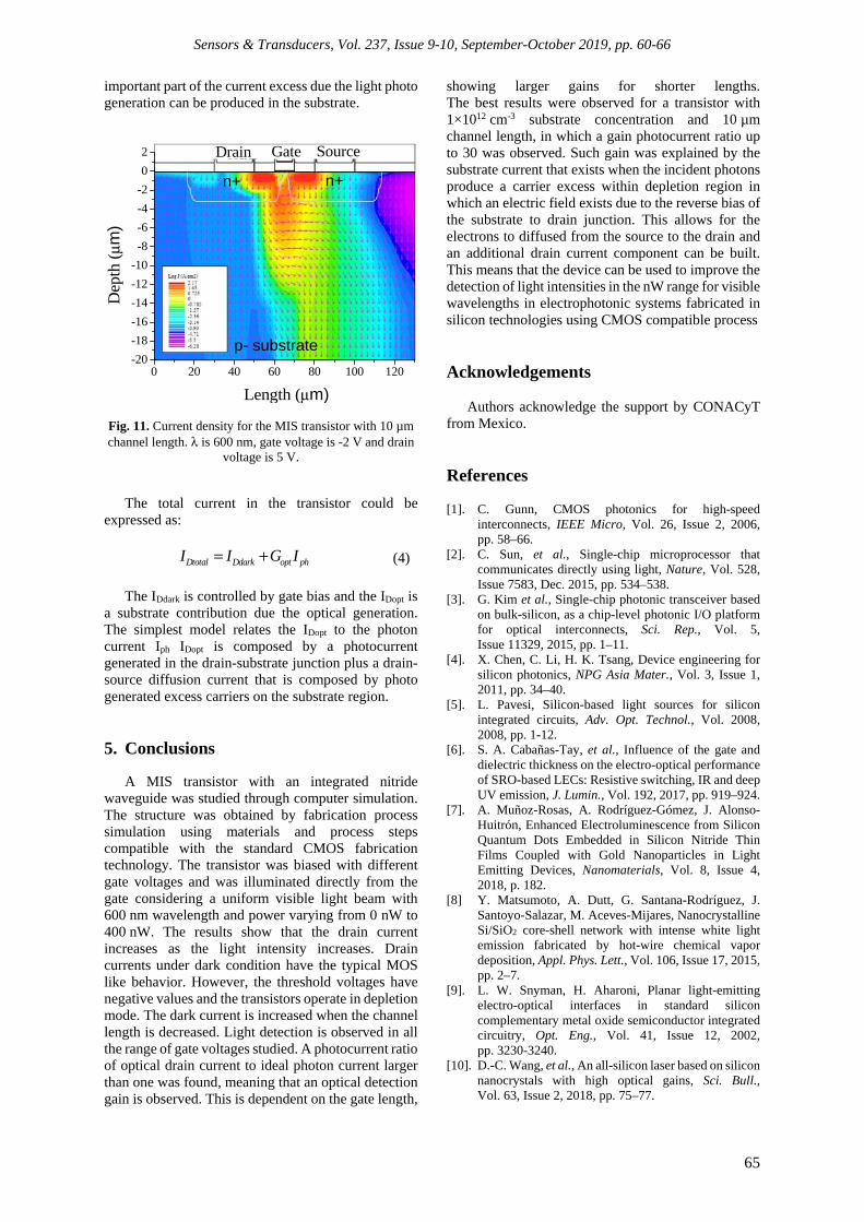
Sensors & Transducers, Vol. 237, Issue 9-10, September-October 2019, pp. 60-66
65
important part of the current excess due the light photo generation can be produced in the substrate.
0 20 40 60 80 100 120-20
-18
-16
-14
-12
-10
-8
-6
-4
-2
0
2
n+
SourceSource
n+
SourceGateDrain
Dep
th (
μm)
p- substrate
Length (μm)
Fig. 11. Current density for the MIS transistor with 10 µm channel length. λ is 600 nm, gate voltage is -2 V and drain
voltage is 5 V.
The total current in the transistor could be expressed as:
Dtotal Ddark opt phI I G I= + (4)
The IDdark is controlled by gate bias and the IDopt is
a substrate contribution due the optical generation. The simplest model relates the IDopt to the photon current Iph IDopt is composed by a photocurrent generated in the drain-substrate junction plus a drain-source diffusion current that is composed by photo generated excess carriers on the substrate region.
5. Conclusions
A MIS transistor with an integrated nitride waveguide was studied through computer simulation. The structure was obtained by fabrication process simulation using materials and process steps compatible with the standard CMOS fabrication technology. The transistor was biased with different gate voltages and was illuminated directly from the gate considering a uniform visible light beam with 600 nm wavelength and power varying from 0 nW to 400 nW. The results show that the drain current increases as the light intensity increases. Drain currents under dark condition have the typical MOS like behavior. However, the threshold voltages have negative values and the transistors operate in depletion mode. The dark current is increased when the channel length is decreased. Light detection is observed in all the range of gate voltages studied. A photocurrent ratio of optical drain current to ideal photon current larger than one was found, meaning that an optical detection gain is observed. This is dependent on the gate length,
showing larger gains for shorter lengths. The best results were observed for a transistor with 1×1012 cm-3 substrate concentration and 10 µm channel length, in which a gain photocurrent ratio up to 30 was observed. Such gain was explained by the substrate current that exists when the incident photons produce a carrier excess within depletion region in which an electric field exists due to the reverse bias of the substrate to drain junction. This allows for the electrons to diffused from the source to the drain and an additional drain current component can be built. This means that the device can be used to improve the detection of light intensities in the nW range for visible wavelengths in electrophotonic systems fabricated in silicon technologies using CMOS compatible process Acknowledgements
Authors acknowledge the support by CONACyT from Mexico. References [1]. C. Gunn, CMOS photonics for high-speed
interconnects, IEEE Micro, Vol. 26, Issue 2, 2006, pp. 58–66.
[2]. C. Sun, et al., Single-chip microprocessor that communicates directly using light, Nature, Vol. 528, Issue 7583, Dec. 2015, pp. 534–538.
[3]. G. Kim et al., Single-chip photonic transceiver based on bulk-silicon, as a chip-level photonic I/O platform for optical interconnects, Sci. Rep., Vol. 5, Issue 11329, 2015, pp. 1–11.
[4]. X. Chen, C. Li, H. K. Tsang, Device engineering for silicon photonics, NPG Asia Mater., Vol. 3, Issue 1, 2011, pp. 34–40.
[5]. L. Pavesi, Silicon-based light sources for silicon integrated circuits, Adv. Opt. Technol., Vol. 2008, 2008, pp. 1-12.
[6]. S. A. Cabañas-Tay, et al., Influence of the gate and dielectric thickness on the electro-optical performance of SRO-based LECs: Resistive switching, IR and deep UV emission, J. Lumin., Vol. 192, 2017, pp. 919–924.
[7]. A. Muñoz-Rosas, A. Rodríguez-Gómez, J. Alonso-Huitrón, Enhanced Electroluminescence from Silicon Quantum Dots Embedded in Silicon Nitride Thin Films Coupled with Gold Nanoparticles in Light Emitting Devices, Nanomaterials, Vol. 8, Issue 4, 2018, p. 182.
[8] Y. Matsumoto, A. Dutt, G. Santana-Rodríguez, J. Santoyo-Salazar, M. Aceves-Mijares, Nanocrystalline Si/SiO2 core-shell network with intense white light emission fabricated by hot-wire chemical vapor deposition, Appl. Phys. Lett., Vol. 106, Issue 17, 2015, pp. 2–7.
[9]. L. W. Snyman, H. Aharoni, Planar light-emitting electro-optical interfaces in standard silicon complementary metal oxide semiconductor integrated circuitry, Opt. Eng., Vol. 41, Issue 12, 2002, pp. 3230-3240.
[10]. D.-C. Wang, et al., An all-silicon laser based on silicon nanocrystals with high optical gains, Sci. Bull., Vol. 63, Issue 2, 2018, pp. 75–77.

Sensors & Transducers, Vol. 237, Issue 9-10, September-October 2019, pp. 60-66
66
[11]. K. Nishiguchi, Y. Ono, A. Fujiwara, H. Yamaguchi, H. Inokawa, Y. Takahashi, Infrared detection with silicon nano-field-effect transistors, Appl. Phys. Lett., Vol. 90, Issue 22, 2007, pp. 223108-1 – 223108-3.
[12]. S. V. Averin, P. I. Kuznetzov, V. A. Zhitov, N. V. Alkeev, Solar-blind MSM-photodetectors based on Al x Ga 1-x N heterostructures, Opt. Quantum Electron., Vol. 39, Issue 3, 2007, pp. 181–192.
[13]. W. Zhang, M. Chan, R. Huang, P. K. Ko, High gain gate/body tied NMOSFET photo-detector on SOI substrate for low power applications, Solid. State. Electron., Vol. 44, Issue 3, 2000, pp. 535–540.
[14]. A. A. González-Fernández, J. Juvert, M. Aceves-Mijares, C. Domínguez, Monolithic Integration of a Silicon-Based Photonic Transceiver in a CMOS Process, IEEE Photonics J., Vol. 8, Issue 1, 2016.
[15]. K. Xu, N. Ning, K. A. Ogudo, J.-L. Polleux, Q. Yu, L. W. Snyman, Light emission in silicon: from device physics to applications, in Proceedings of the International Workshop on Thin Films for Electronics, Electro-Optics, Energy, and Sensors, 2015, p. 966702.
[16]. K. Misiakos, et al., All-Silicon Spectrally Resolved Interferometric Circuit for Multiplexed Diagnostics: A Monolithic Lab-on-a-Chip Integrating All Active and Passive Components, ACS Photonics, Vol. 6, Issue 7, 2019, pp. 1694–1705.
[17]. J. Alarcón-Salazar, G. V. Vázquez, A. A. González-Fernández, I. E. Zaldívar-Huerta, J. Pedraza-Chávez,
M. Aceves-Mijares, Waveguide-detector system on silicon for sensor application, Adv. Mater. Lett., Vol. 9, Issue 2, 2018, pp. 116–122.
[18]. J. Hernández-Betanzos, A. A. Gonzalez-Fernandez, J. Pedraza, and M. Aceves-Mijares, Effect of the channel length in the response of a MIS transistor sensor with optical gain for nano-watts light signal, in Proceedings of the 5th International Conference on Sensors and Electronic Instrumentation Advances (SEIA’19), Tenerife (Canary Islands), Spain, 25-27 September 2019,, pp. 214-215.
[19]. Athena User’s Manual, SILVACO, Inc., 2013. [20]. Atlas User’s Manual, SILVACO, Inc., 2015. [21]. S. M. Sze, Semiconductor Devices. Physics and
Technology, 3rd ed., Wiley, 2012. [22]. M. Green, Self-consistent optical parameters of
intrinsic silicon at 300 K including temperature coefficients, Sol. Energy Mater. Sol. Cells, Vol. 92, Issue 11, 2008, pp. 1305–1310.
[23]. H. K. Zimmermann, Integrated Silicon Optoelectronics, Springer Berlin Heidelberg, Berlin, Heidelberg, Vol. 148, 2010.
[24]. M. A. Green, M. J. Keevers, Optical properties of intrinsic silicon at 300 K, Prog. Photovoltaics Res. Appl., Vol. 3, Issue 3, 1995, pp. 189–192.
__________________
Published by International Frequency Sensor Association (IFSA) Publishing, S. L., 2019 (http://www.sensorsportal.com).

Sensors & Transducers, Vol. 237, Issue 9-10, September-October 2019, pp. 67-74
67
Sensors & Transducers
Published by IFSA Publishing, S. L., 2019 http://www.sensorsportal.com
Optimized Integrated PIN Photodiodes with Improved Backend Layers
* Ingrid JONAK-AUER, Frederic ROGER and Olesia SYNOOKA
ams AG, Device R&D, Tobelbaderstrasse 30, 8141 Premstaetten, Austria * Tel.: +43-3136-500-32000, fax: +43-3136-500-932000
* E-mail: [email protected]
Received: 30 August 2019 /Accepted: 27 September 2019 /Published: 30 November 2019 Abstract: This paper constitutes a systematic analysis of the impact of low-doped intrinsic base material, different bottom anti-reflective coatings and dielectric filter deposition on the electrical and optical performance of Si photodiodes processed in standard CMOS fabrication processes. Photodiode designs cover full area as well as interdigitated variants. Optimization of the photodiode’s spectral responsivity for a specific wavelength has been achieved by different bottom anti-reflective coating concepts as well as direct deposition of interference filters on Si-wafer. While standard bottom anti-reflective coating is the most efficient way of optimizing the optical response, embedded bottom anti-reflective coating offers the possibility of additional interference filter deposition directly on the wafer. For full area photodiodes with respective anti-reflective coating in place, the photodiode’s quantum efficiency approaches 100 % for λ=750 nm. For interdigitated photodiodes, the spectral responsivity in the wavelength range of 400 nm to 500 nm can be significantly enhanced compared to full area photodiodes and show values as high as 0.21 A/W @ 400 nm and 0.37 A/W @ 500 nm. Optimized blue photodiodes are not sensible to iEPI thicknesses and have a leakage current of 10 pA for a 150 µm×150 µm square photodiode. Keywords: Integrated PIN Photodiode, Intrinsic epitaxial Si substrate, Bottom antireflective coating, Dielectric Filter, Spectral responsivity, Leakage current.
1. Introduction
A photodiode (PD) is a device based on a p-n junction collecting photocurrent generated in the substrate. The combination of reverse biasing and large depletion area are necessary for improving the quantum efficiency of the photodiode [1]. The depletion area can be enlarged by using low-doped intrinsic Si, thus forming a p-intrinsic-n (PIN) photodiode. The low-doped intrinsic epitaxial material (iEPI) additionally reduces the recombination rate of the photo carriers, thus improving the efficiency of the device. The ability to detect only a defined portion (“band”) of incoming light with respect to wavelength
is key for applications such as color sensing, spectral imaging, UV light detection and ambient light sensing. The photodiode can be tuned to be especially sensitive to specific wavelengths by using appropriate p-n junctions as well as adding a variety of add-on filters and coatings like bottom anti reflective coating (BARC), embedded bottom anti reflective coating (eBARC) and/or dielectric filters as part of the CMOS fabrication process, In this paper the impact of the different intrinsic p-type base materials, different photodiode and guard ring designs and different add-on layers are analyzed with respect to optical and electrical performance of the optical sensors.
http://www.sensorsportal.com/HTML/DIGEST/P_3112.htm
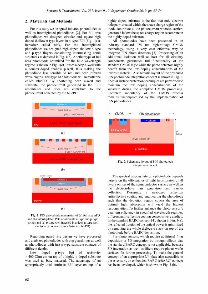
Sensors & Transducers, Vol. 237, Issue 9-10, September-October 2019, pp. 67-74
68
2. Materials and Methods
For this study we designed full area photodiodes as well as interdigitated photodiodes [2]. For full area photodiodes we designed circular and square high doped shallow n-type layers in p-type iEPI (Fig. 1(a)), hereafter called nPD, For the interdigitated photodiodes we designed high doped shallow n-type and p-type fingers constituting intermeshing comb structures as depicted in Fig. 1(b). Another type of full area photodiode optimized for the blue wavelength regime is shown in Fig. 1(c). It uses a deep n-well with a counter-doped shallow p-well, thus making the photodiode less sensible to red and near infrared wavelengths. This type of photodiode will hereafter be called bluePD. By shortening deep n-well and substrate, the photocurrent generated in the iEPI recombines and does not contribute to the photocurrent collected by the bluePD.
(a)
(b)
(c)
Fig. 1. PIN photodiode schematics of (a) full area nPD
and (b) interdigitated PDs of alternate n-type and p-type stripes and (c) p-type well inserted in a deep n-type well
electrically connected to substrate (bluePD).
Regarding guard ring design we have processed and analyzed photodiodes with pnp guard rings as well as photodiodes with just p-type substrate contacts of different depths.
Low doped p-type Epi of resistivity > 400 Ohm-cm on top of a highly p-doped substrate was used as base material. The advantage of an appropriately thick intrinsic EPI layer on top of a
highly doped substrate is the fact that only electron hole pairs created within the space charge region of the diode contribute to the photocurrent whereas carriers generated below the space charge region recombine in the highly doped substrate
All photodiodes have been processed in an industry standard 350 nm high-voltage CMOS technology, using a very cost effective way to integrate PIN photo detectors [3]. Processing of an additional isolation well as host for all circuitry components guarantees full functionality of the standard CMOS logic while the photo detectors highly benefit from the low doping concentrations of the intrinsic material. A schematic layout of the presented PIN photodiode integration concept is shown in Fig. 2. Special surface protection techniques are performed to maintain the low doping concentrations of the substrate during the complete CMOS processing. Complete modularity of the CMOS process remains uncompromised by the implementation of PIN photodiodes.
Fig. 2. Schematic layout of PIN photodiode integration concept.
The spectral responsivity of a photodiode depends largely on the efficiencies of light transmission of all layers on top of the semiconductor surface as well as the electron-hole pair generation and carrier collection. Designing a near-zero reflection antireflective coating and engineering the photodiode such that the depletion region covers the area of optimal light absorption will yield the highest responsivities. To further enhance the photo sensor’s quantum efficiency in specified wavelength regimes, different anti-reflective coating concepts were applied. In the standard BARC concept [4], shown in Fig. 3(a), the reflected fraction of the optical power is minimized by removing the whole dielectric stack on top of the photodiode before BARC deposition.
For photo sensors, which require additional filter deposition or 3D integration by through silicon vias the standard BARC concept is not applicable, because 3D integration as well as filters require planar wafer surfaces for further processing. To make the general concept of an appropriate λ/4 plate also accessible to these sensors, an embedded BARC (eBARC) concept has been developed, which is shown in Fig. 3 (b).

Sensors & Transducers, Vol. 237, Issue 9-10, September-October 2019, pp. 67-74
69
Fig. 3(a). Schematics of standard BARC concept.
Fig. 3(b). Schematics of embedded BARC concept.
Some photodiodes were processed with dielectric filter stacks in addition to eBARC. Interference filter processing uses reactive magnetron sputtering and lift-off patterning, which permits lateral filter dimensions smaller than 100 µm. Band pass filters were designed for transmission of different spectral regimes and processed in-line with the photodiodes. Special care was taken by layout rules and wafer edge treatment to minimize mechanical stress and wafer bow for combinations of up to 6 and more filters integrated on the wafer.
Characterization of the PIN photodiodes covers capacitance and leakage current measurements as well as spectral responsivity measurements. Photodiode layout permits direct pad access to anode and cathode without any signal amplification circuit. Capacitance measurements have been performed with a Cascade Micromanipulator and a HP4284A precision LCR meter, for leakage current measurements we used the Cascade Micromanipulator equipped with thermo-chuck and a Parameter Analyzer HP4155B. All optical measurements were performed on wafer level according to the measurement setup depicted in Fig. 4. A Xenon lamp is used as light source, which is discrete band filtered in 1 nm wavelength steps via a spectrometer. The monochromatic light beam is split, one half goes into a reference detector for actual power measurement, while the other half is fed onto the optically active area of the device under test. To determine the responsivity of the device under test, the photocurrent generated by the incident light power is measured with a Parameter Analyzer HP4155B. The
biasing of the photodetector device under test is also done by the Parameter Analyzer. Measurement data recordings as well as filter steering, calibration and reference light power measurements are controlled via serial bus interfaces and personal computers.
Fig. 4. Experimental setup for spectral responsivity measurements.
3. Results Fig. 5 presents the impact of the iEPI- and BARC-
thickness on spectral responsivity (SR). The spectral responsivity reaches 100 % of the quantum efficiency for BARC layers optimized for λ=750 nm and λ=900 nm and 82 % for layer optimized for λ=425 nm wavelengths.
Fig. 5. Dependence of spectral responsivity on iEPI- and BARC-thickness.
The leakage current of a circular nPD of 365 µm diameter in dependence on iEPI- and BARC-thickness is shown in Fig. 6.

Sensors & Transducers, Vol. 237, Issue 9-10, September-October 2019, pp. 67-74
70
Fig. 6. Leakage current dependence on iEPI- and BARC thickness.
From a theoretical point of view, thicker iEPI should cause larger space charge width and thus higher leakage current. But TCAD simulations showed no such effect as depicted in Fig. 7, where the leakage current of nPDs has been simulated for 20 µm and 30 µm iEPI.
Fig. 7. TCAD simulation of nPD leakage current for two EPI thicknesses.
Essentailly we could confirm by TCAD simulations, that the increased leakage of the nPD in 30 µm iEPI was caused by lower doping of the 30 µm iEPI in comparison to the 20 µm iEPI. Figs. 8 and 9 show the extension of the space charge region in dependence on the EPI doping concentration and according leakage current simulations, respectively. The simulation results show the same trend as our measurements. Significant difference in leakage current of photodiodes processed on iEPI of different thickness can be observed only for very lowly doped materials. As depicted in Fig. 10, photodiodes processed on 20 µm and 30 µm iEPI show diverging leakage values only for doping concentrations lower than 1E13/cm³ corrresponding to resistivity values higher than 1 kOhm-cm. Lower leakage of photodiodes in thinner iEPI is caused by the limited extension of the space charge region in depth due to the low resistive substrate placed below the iEPI layer.
Fig. 8. TCAD simulation of space charge region extension in dependence on EPI doping.
Fig. 9. TCAD simulation of nPD leakae current for different EPI resistivity.
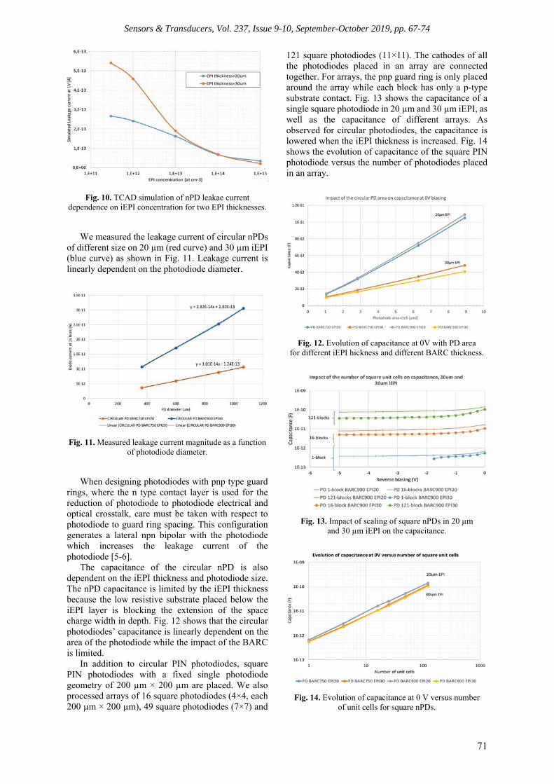
Sensors & Transducers, Vol. 237, Issue 9-10, September-October 2019, pp. 67-74
71
Fig. 10. TCAD simulation of nPD leakae current dependence on iEPI concentration for two EPI thicknesses.
We measured the leakage current of circular nPDs of different size on 20 µm (red curve) and 30 µm iEPI (blue curve) as shown in Fig. 11. Leakage current is linearly dependent on the photodiode diameter.
Fig. 11. Measured leakage current magnitude as a function of photodiode diameter.
When designing photodiodes with pnp type guard rings, where the n type contact layer is used for the reduction of photodiode to photodiode electrical and optical crosstalk, care must be taken with respect to photodiode to guard ring spacing. This configuration generates a lateral npn bipolar with the photodiode which increases the leakage current of the photodiode [5-6].
The capacitance of the circular nPD is also dependent on the iEPI thickness and photodiode size. The nPD capacitance is limited by the iEPI thickness because the low resistive substrate placed below the iEPI layer is blocking the extension of the space charge width in depth. Fig. 12 shows that the circular photodiodes’ capacitance is linearly dependent on the area of the photodiode while the impact of the BARC is limited.
In addition to circular PIN photodiodes, square PIN photodiodes with a fixed single photodiode geometry of 200 µm × 200 µm are placed. We also processed arrays of 16 square photodiodes (4×4, each 200 µm × 200 µm), 49 square photodiodes (7×7) and
121 square photodiodes (11×11). The cathodes of all the photodiodes placed in an array are connected together. For arrays, the pnp guard ring is only placed around the array while each block has only a p-type substrate contact. Fig. 13 shows the capacitance of a single square photodiode in 20 µm and 30 µm iEPI, as well as the capacitance of different arrays. As observed for circular photodiodes, the capacitance is lowered when the iEPI thickness is increased. Fig. 14 shows the evolution of capacitance of the square PIN photodiode versus the number of photodiodes placed in an array.
Fig. 12. Evolution of capacitance at 0V with PD area for different iEPI hickness and different BARC thickness.
Fig. 13. Impact of scaling of square nPDs in 20 µm and 30 µm iEPI on the capacitance.
Fig. 14. Evolution of capacitance at 0 V versus number of unit cells for square nPDs.

Sensors & Transducers, Vol. 237, Issue 9-10, September-October 2019, pp. 67-74
72
The capacitance is varying linearly with the number of blocks. As each block has a fixed geometry, the capacitance is varying linearly with the area of the array.
For photodiodes with p-type substrate contact rings instead of pnp guard rings, increasing depth of the p-type substrate contact ring causes decreasing leakage current and increasing capacitance of the photodiodes [3]. The dependence of photodiode leakage and capacitance on the distance between deep p-type substrate contact ring and photodiode is shown in Figs. 15 and 16, respectively. nPDs with 2 µm, 5 µm and 10 µm distance between substrate contact ring and photodiode were analyzed. The base material was 20 µm iEPI. While leakage current shows hardly any dependence on distance, capacitance values vary significantly.
Fig. 15. Impact of nPD distance to deep-p substrate contact on leakage current.
Fig. 16. Impact of nPD distance to deep-p substrate contact on capacitance.
Interdigitated photodiodes (Fig. 1(b)) target for short wavelength light (UV – blue), which is absorbed very close to the Si surface [7]. Therefore UV-blue light is very sensitive to recombination effects due to high doped surface layers. As for our photodiode design the active area between n- and p-fingers is lowly doped, recombination effects are significantly reduced. Electron-hole pairs are created close to the Si surface and the lateral electric field between the fingers collects the generated charge, thus
significantly improving the optical response in the respective wavelength range even at 0 V biasing. Fig. 17 shows the influence of finger spacing on spectral responsivity and compares interdigitated photodiodes to nPDs (red curve). For 1.2 µm finger spacing spectral responsivity values as high as 0.21 A/W @ 400 nm and 0.37 A/W @ 500 nm could be achieved.
Fig. 17. Influence of finger spacing of interdigitated PDs on spectral responsivity.
Unfortunately, due to the internal npn bipolar action between the n-type and p-type fingers, the leakage current is much stronger with respect to an nPD leakage current as shown in Fig. 18.
Fig. 18. Leakage current comparison between Interdigitated PDs (blue and green curves) with different
n-type/p-type fingers spacing and nPD (red curve).
For the optimized bluePD (Fig. 1(c)), the impact of iEPI thickness on the spectral responsivity is limited due to the fact, that collection photogenerated carriers from UV-blue light happens very close to the Si surface. Fig. 19 shows gray and blue spectral responsivity curves for blue PDs processed on 20 µm and 30 µm thick iEpi material, respectively. There is no difference in spectral responsivity to be seen for the different base materials. The yellow curve represents the spectral responsivity result for a blue PD processed with a BARC layer optimized for λ=425 nm. The

Sensors & Transducers, Vol. 237, Issue 9-10, September-October 2019, pp. 67-74
73
increased spectral response due to the BARC is clearly visible.
Fig. 19. Spectral responsivity for bluePD as a function of iEPI thickness and BARC optimization.
Because of the internal structure of the bluePD, the leakage current is not dependent on the iEPI thickness, either, and is around 10 pA at a biasing below -1 V for a 150 µm × 150 µm photodiode size designed in a square configuration as can be seen in Fig. 20.
Fig. 20. Leakage Current for bluePD as a function of iEPI thickness and BARC optimization.
Implementation of filter technologies is key for applications such as color sensing, spectral imaging, and ambient light sensing. The required spectral transmission characteristics of the filters is frequently determined by industry standards and customer requests. State of the art and commercially available interference filters deposited on glass or specifically absorbing glasses can be used for such applications. However, for monolithic integrated smart sensors, as described in this paper, the required integration density can’t be reached with filters on glass substrates. The filters have to be part of the CMOS fabrication process, taking advantage of the available lithography steps. ams AG offers a large variety of inorganic filters as part of their CMOS fabrication processes, which can be utilized as stand-alone filters together with a photodiode, or in combination as stacked filters.
In order to check the influence of interference filter deposition and patterning on photodiode behaviour, we performed leakage current and spectral responsivity measurements on nPDs with eBARC optimized for 900 nm as well as long pass filters cutting off wavelengths below 850 nm. Fig. 21 shows the spectral responsivity curves for filter devices on 20 µm and 30 µm thick iEPI base material. Fig. 22 shows the leakage current comparison between the filter device described above and the same device processed without filters. Both devices were processed on 20 µm thick iEPI base material. It can be seen that the filter device shows higher leakage, which is most likely caused by the enhanced mechanical stress on the wafers due to filter deposition.
Fig. 21. Influence of long pass filter deposition on spectral responsivity.
Fig. 22. Influence of long pass filter deposition on leakage current.
4. Conclusions
In this paper, we present the impact of low-doped intrinsic Si Epi material and various backend coatings (BARC, eBARC and filter) on the optical and electrical performance of various PIN photodiodes. Full area PIN photodiodes (high doped n-cathode in p- epitaxial layer) reach a spectral responsivity of 0.63 A/W and 100 % quantum efficiency with the deposition of BARC optimized for λ>750 nm. The leakage current is larger with thicker iEPI thickness and varies from 3.5 pA (20 µm iEPI) to 10 pA (30 µm

Sensors & Transducers, Vol. 237, Issue 9-10, September-October 2019, pp. 67-74
74
iEPI) for photodiodes with 365, diameter at 1V reverse biasing. Their capacitance is reduced for larger iEPI thickness and varies from 0.97 pF (30 µm iEPI) to 1.43 pF (20 µm iEPI) at 0 V biasing. Further tuning of capacitance is possible by distance variations to the surrounding guard rings and substrate contacts. For interdigitated photodiodes, the spectral responsivity in the wavelength range 400 nm to 500 nm can be significantly enhanced compared to full area photodiodes and show values as high as 0.21 A/W @ 400 nm and 0.37 A/W @ 500 nm. Optimized blue photodiodes are not sensible to iEPI thicknesses and have a leakage current of 10 pA for a 150 µm × 150 µm square photodiode.
References [1]. Simon M. Sze, Kwok K. Ng, Physics of semiconductor
devices, 3rd edition, John Wiley & Sons, Inc., Hoboken, NJ, USA, 2007, pp. 671-682.
[2]. I. Jonak-Auer, et al., Monolithic integrated PIN photodiode study with backend stack optimization, in
Proceedings of the 5th International Conference on Sensors Engineering and Electronics Instrumentation Advances (SEIA'19), Tenerife (Canary Islands), Spain, 25-27 September 2019, pp. 92-99.
[3]. I. Jonak-Auer, et al., New integration concept of PIN photodiodes in 0.35 µm CMOS technologies, in Proceedings of the SPIE, Vol. 8431, 2012.
[4]. I. Jonak-Auer, et al., PIN photodiodes with significantly improved responsivities implemented in a 0.35 μm CMOS/BiCMOS technology, in Proceedings of the SPIE, 7719, 77190U, 2010.
[5]. Jordi Teva, et al., Dark current study for CMOS fully integrated-PIN-photodiodes, in Proceedings of the SPIE - The International Society for Optical Engineering, Vol. 8073, Optical Sensors 2011; and Photonic Crystal Fibers V; 80731P, 2011.
[6]. Jordi Teva, et al., Gathering effect on Dark Current for CMOS fully integrated-, PIN- photodiodes, in Proceedings of the SPIE - The International Society for Optical Engineering, Vol. 7605, 2010.
[7]. H. Zimmermann, et al., Blue-Enhanced PIN Finger Photodiodes in a 0.35-µm SiGe BiCMOS Technology, IEEE Photonics Technology Letters, Vol. 21, Issue 22, 2009.
__________________
Published by International Frequency Sensor Association (IFSA) Publishing, S. L., 2019 (http://www.sensorsportal.com).

Sensors & Transducers, Vol. 237, Issue 9-10, September-October 2019, pp. 75-79
75
Sensors & Transducers
Published by IFSA Publishing, S. L., 2019 http://www.sensorsportal.com
A Miniaturized Ultra Wide-band Band-pass Filter for the Tenerife Microwave Spectrometer
1, 2, * Javier DE MGUEL-HERNÁNDEZ and 1, 2 Roger J. HOYLAND
1 Instituto de Astrofísica de Canarias, E-38200 La Laguna, Tenerife, Spain 2 Departamento de Astrofísica, Universidad de La Laguna, E-38206 La Laguna, Tenerife, Spain
* E-mail: [email protected]
Received: 30 August 2019 /Accepted: 27 September 2019 /Published: 30 November 2019 Abstract: The QUIJOTE Experiment has been built to study the polarization of the Cosmic Microwave Background (CMB). The study of the CMB provides one of the most powerful tools in modern cosmology. In particular, CMB polarization offers a new window onto the inflationary phase of the Universe, some 10-35 seconds after the Big Bang. Measurement of the CMB spectrum to an accuracy that will reveal interesting science (micro-kelvin variations) is particularly difficult because there are many systematics that lead to effects higher than this level. There are several instruments that have been designed for CMB spectral measurement (FIRAS-COBE, ARCADE, PIXIE). The present plan is to extend the goals of QUIJOTE by building a new and unique microwave spectrometer in the frequency range 10-20 GHz, with the aim of characterizing the spectral signals associated with the reionization epoch and dark ages in the Universe. This document describes the first component for the Tenerife Microwave Spectrometer (TMS), an ultra-wideband bandpass filter (BPF). A filter prototype covering the 10-20 GHz band has been successfully designed, manufactured, and measured in the laboratory to compare results and simulations. Keywords: Cosmic microwave background, Radio-astronomy, Microwaves, Cosmology, Ultra-wide band, Filters. 1. Introduction
In this section, the TMS is briefly described. Fig. 1
shows the preliminary schematic diagram of a microwave spectrometer for measuring CMB spectra between 10 and 20 GHz. In order to achieve sufficient sensitivity the front end of a radiometer is cooled in a cryostat to 4-10 K. The cryogenic reference load, opto-mechanics, and ultra-LNAs are cooled by a 4 K closed cycle helium gas cooler and maintained at a constant temperature slightly higher than 4 K by actively heating the cold stage.
The radiometer consists of a pair of feedhorns, one pointed at a cold black body and the other looking out of the cryostat through a transparent window. These
feedhorns are both followed by broad-band 10-20 GHz waveguide OMTs to couple the two linear polarizations. The polar outputs of both sky and load horns are fed to either arm of a radiometer correlator that employs both cold and warm gain and 180o broad-band phase switch to switch the outputs. The correlating elements are 90o hybrid couplers or ridged waveguide hybrid tees. Each correlator contains two similar LNAs with a noise temperature lower than 10 K followed by further amplification and a 180o phase switch in each branch. The phase switches are housed in the BEM. Finally, the load and sky signals are decorrelated in a similar 90o hybrid coupler or ridged waveguide hybrid tee to that of the input. The outputs of these two hybrids are sent to the novel full-
http://www.sensorsportal.com/HTML/DIGEST/P_3113.htm

Sensors & Transducers, Vol. 237, Issue 9-10, September-October 2019, pp. 75-79
76
band FT-spectrometers bank. The DC output is amplified and then digitized for post processing in an ADC unit.
Regarding the detector unit, a novel correlator based on a Fourier filter chain is being developed. An elegant and simple three-channel design of a
Reflection Mode Discriminator receiver for IFM has been converted into an innovative wideband autocorrelator for a novel Fourier Transform technique based spectrometer. See reference [8] in order to know more.
Fig. 1. TMS General Schematic.
In this device, three channels with relative phase-
shifts of 0, 120 and 240 degrees produce three signal-output voltages.
Each of the three channels introduces a total path delay in the signal by using delay path length and differential impedance in the transmission lines.
The unit uses square law detectors being able to extract the real voltage signal. In this development, the 75 Ohm resistance is formed by a parallel square law detector (diode+resistor) and since power and voltage are π/2 shifted, at frequencies where the electric length of a short circuited line is a m multiple of λ/2 all the input power will be dissipated in the resistor, whereas at n odd multiples of λ/4 the resistor and there the detector sees no power because of a SWR effect. This situation is inverted for a line finished with an open circuit. This is represented in the Fig. 2.
Regarding the wide band feedhorns, we have developed a new technique based on metamaterials in order to design an innovative meta-rings system, improving the behavior of the corrugated horns in a consistent way.
It can be demonstrated that the surface impedance of a horn walls is the more important characteristic in order to keep the values of cross-polarization levels,
side-lobe levels, return-loss, etc. under reasonable limits for observations in radioastronomy. Thus, our metahorn design is able to give a 2:1 bandwidth factor or more for first time.
Fig. 2. Power standing wave pattern for a short circuited transmission line (left) and for a transmission line finished
in an open circuit (right).
This novel design and its theory can be consulted in the references [9] and [10].
Here, an element to design now is a microwave filter covering the entire band, of the experiment; that is, with a 2:1 bandwidth factor, which is challenging since most microwave filters are designed to cover a few tens or hundreds of megahertz.
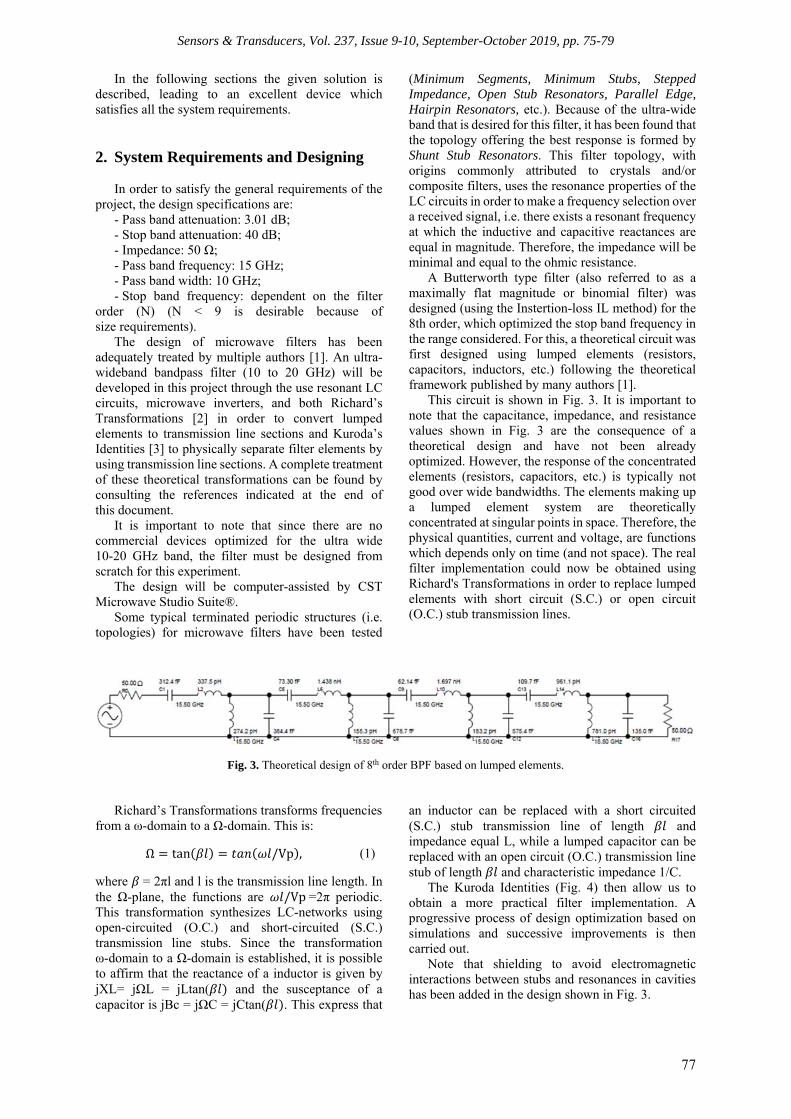
Sensors & Transducers, Vol. 237, Issue 9-10, September-October 2019, pp. 75-79
77
In the following sections the given solution is described, leading to an excellent device which satisfies all the system requirements.
2. System Requirements and Designing
In order to satisfy the general requirements of the
project, the design specifications are: - Pass band attenuation: 3.01 dB; - Stop band attenuation: 40 dB; - Impedance: 50 Ω; - Pass band frequency: 15 GHz; - Pass band width: 10 GHz; - Stop band frequency: dependent on the filter
order (N) (N < 9 is desirable because of size requirements).
The design of microwave filters has been adequately treated by multiple authors [1]. An ultra-wideband bandpass filter (10 to 20 GHz) will be developed in this project through the use resonant LC circuits, microwave inverters, and both Richard’s Transformations [2] in order to convert lumped elements to transmission line sections and Kuroda’s Identities [3] to physically separate filter elements by using transmission line sections. A complete treatment of these theoretical transformations can be found by consulting the references indicated at the end of this document.
It is important to note that since there are no commercial devices optimized for the ultra wide 10-20 GHz band, the filter must be designed from scratch for this experiment.
The design will be computer-assisted by CST Microwave Studio Suite®.
Some typical terminated periodic structures (i.e. topologies) for microwave filters have been tested
(Minimum Segments, Minimum Stubs, Stepped Impedance, Open Stub Resonators, Parallel Edge, Hairpin Resonators, etc.). Because of the ultra-wide band that is desired for this filter, it has been found that the topology offering the best response is formed by Shunt Stub Resonators. This filter topology, with origins commonly attributed to crystals and/or composite filters, uses the resonance properties of the LC circuits in order to make a frequency selection over a received signal, i.e. there exists a resonant frequency at which the inductive and capacitive reactances are equal in magnitude. Therefore, the impedance will be minimal and equal to the ohmic resistance.
A Butterworth type filter (also referred to as a maximally flat magnitude or binomial filter) was designed (using the Instertion-loss IL method) for the 8th order, which optimized the stop band frequency in the range considered. For this, a theoretical circuit was first designed using lumped elements (resistors, capacitors, inductors, etc.) following the theoretical framework published by many authors [1].
This circuit is shown in Fig. 3. It is important to note that the capacitance, impedance, and resistance values shown in Fig. 3 are the consequence of a theoretical design and have not been already optimized. However, the response of the concentrated elements (resistors, capacitors, etc.) is typically not good over wide bandwidths. The elements making up a lumped element system are theoretically concentrated at singular points in space. Therefore, the physical quantities, current and voltage, are functions which depends only on time (and not space). The real filter implementation could now be obtained using Richard's Transformations in order to replace lumped elements with short circuit (S.C.) or open circuit (O.C.) stub transmission lines.
Fig. 3. Theoretical design of 8th order BPF based on lumped elements.
Richard’s Transformations transforms frequencies
from a ω-domain to a Ω-domain. This is: Ω tan /Vp , (1)
where = 2πl and l is the transmission line length. In the Ω-plane, the functions are /Vp=2π periodic. This transformation synthesizes LC-networks using open-circuited (O.C.) and short-circuited (S.C.) transmission line stubs. Since the transformation ω-domain to a Ω-domain is established, it is possible to affirm that the reactance of a inductor is given by jXL= jΩL = jLtan( and the susceptance of a capacitor is jBc = jΩC = jCtan( . This express that
an inductor can be replaced with a short circuited (S.C.) stub transmission line of length and impedance equal L, while a lumped capacitor can be replaced with an open circuit (O.C.) transmission line stub of length and characteristic impedance 1/C.
The Kuroda Identities (Fig. 4) then allow us to obtain a more practical filter implementation. A progressive process of design optimization based on simulations and successive improvements is then carried out.
Note that shielding to avoid electromagnetic interactions between stubs and resonances in cavities has been added in the design shown in Fig. 3.

Sensors & Transducers, Vol. 237, Issue 9-10, September-October 2019, pp. 75-79
78
Fig. 4. Kuroda’s identities (licensed under the Creative Commons Attribution-ShareAlike 3.0 License. Courtesy
Spinningspark at Wikipedia).
3. Prototype Results
The filter was fabricated with an LPKF machine model ProtoMat-S100 on a PCB (Rogers 4003-C) circuit. The objective of the final stage is to compare the simulated model with the manufactured model and the requirements, in case of discrepancies between them, to return to the design stage with the objective of investigating and solving them. Several iterations were necessary. An image of the manufactured filter and the results of the test measurements made on it are shown in Figs. 5 and 6. For the measurements a KeySight model PNA-X N5245A machine was used.
4. Discussion
The preliminary design requirements are successfully satisfied, with an excellent adaptation, correct attenuation in the pass and stop bands and an attenuation better than -10 dB over the entire 10-20 GHz range. Note that, given the design characteristics of the stubs (where the length of the transmission lines is λ/8 at the cut-off frequency), the response is periodically repeated at intervals of four times the cut-off frequency (Fig. 6).
It has been verified that the results of the software simulation and the measurements on the manufactured filter are reasonably similar. This makes it possible to double-check, on the one hand, by checking that the software is reasonably reliable and, on the other hand, that significant errors have not been made during the manufacturing and assembly phase, with the manufacturing tolerances being within a reliable limit.
With a view to future improvement of the design, a trial with computer-assisted optimization has been carried out, with the result that the filter design would be difficult to improve. This enables us to conclude that the design is excellent, and that the results are difficult to surpass.
Fig. 5. 8th order BPF prototype while measuring in the laboratory using SMA-port adaptors.
Fig. 6. 8th order BPF results.
A high quality ultra band-pass filter covering the range 10 to 20 GHz was designed and fabricated to meet the technical specifications. This was a technological challenge, since there are not many references to bandpass filters of such a width in frequency, and those that exist do not present such a satisfactory response.
In addition, it is a robust design of astonishing simplicity and very cheap to manufacture, which would allow its replacement in case of damage due to the filter is relatively compact (dimensions 25.6×3.6 mm approximately), so no additional miniaturization is required. This device will be ready to be installed in the spectrometer and efficiently filter the CMB in the desired spectral range. Acknowledgements
The author wishes to acknowledge the supervision and support of and all the technicians, engineers, scientists, and administrative staff of the Instituto de Astrofísica de Canarias who have participated in the Quijote-CMB Experiment.

Sensors & Transducers, Vol. 237, Issue 9-10, September-October 2019, pp. 75-79
79
References [1]. Pozar David M., Microwave Engineering, 4th edition,
John Wiley & Sons, Inc., 2011, pp. 380-482. [2]. Richards Paul I., Resistor-Transmission-Line Circuits,
Proceedings of the IRE, Vol. 36, Issue 2, February 1948, pp. 217–220.
[3]. Kuroda K., Derivation methods of distributed constant filters from lumped constant filters, Joint Meeting of Kansai Branch of IECE, Japan, October 1952, pp. 32.
[4]. Butterwworth S., On the Theory of Filters Amplifiers, Experimental Wireless and the Wireless Engineer, Vol. 7, Oct. 1930, pp. 536–541.
[5]. Matthaei G., Young L., Jones E. M. T., Microwave Filters, Impedance-Matching Networks, and Coupling Structures, Artech House, Dedham, MA, 1980.
[6]. Rubiño-Martín José Alberto, Rebolo R., Tucci M., Génova-Santos R., Hildebrandt S. R., Hoyland R. J., Herreros Jesus, Gómez-Reñasco F., López-Caraballo, Carlos, Martinez-Gonzalez, Enrique and Vielva, P and Herranz, D and Casas Franciasco, Artal Eduardo, Aja Beatriz, de la Fuente Luisa, Cano Juan L., Villa
Enrique, Mediavilla Angel, Etxeita B., The Quijote CMB Experiment, pp. 127-135, January 2010.
[7]. De Miguel-Hernández J., Hoyland, R., An Ultra-wideband Band-pass Filter for Cosmic Microwave Background Obervtions, in Proceedings of the 5th International Conference on Sensors and Electronic Instrumentation Advances (SEIA' 2019), Tenerife (Canary Islands), Spain, 25-27 September 2019, pp.24-27.
[8]. De Miguel-Hernández, et al., A High Sensitivity Fourier Transform Spectrometer for Cosmic Microwave Background Observations, IEEE Transactions on Instrumentation and Measurement. Manuscript accepted for Publication, October 2019.
[9]. De Miguel-Hernández J., Hoyland R., Fundamentals of Horn Antennas with Cross-polarization levels for Radioastronomy and Satellite Communications, Journal of Instrumentation, JINST, 2019.
[10]. J. De Miguel-Hernández, et al., Manufacturing of 3D-metallic metamaterials for feedhorns used in radioastronomy and satellite communications, Mechanics of Materials, MECMAT. Manuscript accepted for publication, 2019.
__________________
Published by International Frequency Sensor Association (IFSA) Publishing, S. L., 2019 (http://www.sensorsportal.com).

Sensors & Transducers, Vol. 237, Issue 9-10, September-October 2019, pp. 80-87
80
Sensors & Transducers
Published by IFSA Publishing, S. L., 2019 http://www.sensorsportal.com
Novel and Cost-efficient Sensors for the Concentration Measurement of Ammonia and Ammonium
Nitrate Particles
* Mohamed Lamine BOUKHENANE, Nathalie REDON, Jean-Luc WOJKIEWICZ, Caroline DUC and Patrice CODDEVILLE
IMT Lille Douai, Univ. Lille, Atmospheric Sciences and Environmental Engineering Laboratory, (SAGE), 59000 Lille, France
Tel.: +33327712296 E-mail: [email protected]
Received: 30 August 2019 /Accepted: 27 September 2019 /Published: 30 November 2019 Abstract: In the presence of high concentrations of ammonia and nitric acid gas, the formation of ammonium nitrate particles (NH4NO3) is well established at low temperatures. As a result, high concentrations of ammonium nitrate particles are usually observed during the spring and winter period. Due to its semi-volatile nature, the measurement of ammonium nitrate with classical methods based on filter sampling (sampling time ≥ 24 h) introduce severe artifacts. Thus, the main objective of this study is to develop new low-cost sensors able to measure simultaneously and selectively the concentration of ammonium nitrate particles and its gaseous precursor ammonia. Sensors combine two surfaces which are sensitive to ammonia and based on polyaniline nano-composites materials. The mass concentration of ammonium nitrate is determined by measuring the concentration of the ammonia released by heating one of the sensitive surfaces. Sensors show a response to gaseous ammonia at concentrations less than 20 ppb with sensitivity around 0.3 %.ppb-1, and the limit of detection of sensors to ammonium nitrate particles is around 270 µg.m-3 with a sensitivity of 0.0014 %.µg-1.m3. Keywords: Air quality sensors, Ammonium nitrate particles, Gaseous ammonia, Conductive polymer, Polyaniline. 1. Introduction
Gaseous ammonia is one of the main nitrogen compounds found in the troposphere after N2 and N2O [1-2]. Over 80 % of ammonia emissions come from agricultural activities (livestock, fertilizers, soils…) [3]. Ammonia emissions are not considered as a regulated pollutant in the ambient air in Europe, although they are responsible of many adverse effects on the environment including soil acidification and aquatic eutrophication [4]. In addition, ammonia gas can contribute to particulate matter formation by
reacting with acidic species (H2SO4, HNO3, HCl) leading to the formation of secondary aerosols [5].
Atmospheric particulate matter, particularly PM10 and PM2.5 have a significant impact on human health by causing many respiratory diseases (asthma, chronic obstructive pulmonary disease, and lung cancer) [6]. The spatial and temporal variability of PM2.5
composition and mass concentration was studied by many authors [7–10]. Usually, the higher concentrations of particles are observed during the spring and winter period [11]. Indeed, according to a study conducted by Sharma, et al. [12] at Delhi, India,
http://www.sensorsportal.com/HTML/DIGEST/P_3114.htm

Sensors & Transducers, Vol. 237, Issue 9-10, September-October 2019, pp. 80-87
81
during January 2013 to May 2014, the average mass concentration of PM2.5 was estimated at 196 µg.m-3 during winter months (January and December) and at 84 µg.m-3 during the summer period. In another study carried out by Tao, et al. [13] in Chengdu, China, for a period of one month in every season during 2009–2010, the highest seasonal average of PM2.5
concentrations was observed in the winter (225.5±73.2 µg.m-3) and the lowest in the summer (113.5±39.3 µg.m-3). In Europe, the mass concentrations of PM2.5 are often lower than in India and East Asia. The concentration levels ranged between 8 µg.m-3 and 53 µg.m-3 in the winter and from 10 µg.m-3 to 25 µg.m-3 in the spring [14-15]. However, in some regions, it is possible to reach higher daily concentrations of PM2.5, exceeding 80 µg.m-3.
In addition, several species enter into the composition of PM2.5. Among them, sulfate (SO4
2−), nitrate (NO3
-) and ammonium (NH4+) are the
predominant water-soluble ionic species of PM2.5. They represent approximately 20-40 % of PM2.5 [14-15]. Wang, et al. [16] reported that the average mass concentrations of NO3
-, SO42- and NH4
+ species measured from 8-28 November 2011 in Beijing, China, are respectively: 14.7±11.2 µg.m-3, 12.2±9.63 µg.m-3, and 9.13±7.26 µg.m-3. Furthermore, Jiang, et al. [17] estimated respectively their annual mass concentrations from 2014 to 2015 in Zhengzhou, China, at: 20 µg.m-3, 25 µg.m-3 and 15 µg.m-3.
The formation of ammonium nitrate particles NH4NO3 becomes possible in areas characterized by high ammonia and nitric acid concentrations at low temperatures following full neutralization of acidic sulfate. The process is described by the reversible reaction at temperatures below 170°C [18]:
NH3 (g) + HNO3 (g) ↔NH4NO3 (s, aq)
The reaction equilibrium and ammonium nitrate
state depend on the temperature and relative humidity. Due to its semi-volatile nature, ammonium nitrate can evaporate at ambient temperatures ≥ 20°C [19]. Furthermore, nitric acid is mainly formed by oxidation of NO2 by OH radicals (NO2+OH) during the daytime or by hydrolysis of dinitrogen pentoxide (N2O5) during the nighttime [20].
According to Tao, et al. [21], the neutralization of nitrate by ammonia to obtain ammonium nitrate particles becomes evident at [NH4
+]/[SO42-] > 2. This
molar ratio of ammonium to sulfate can be obtained during the spring and winter period.
Since a long time, the measurement of atmospheric particles is carried out with the classical method which is based on filter sampling by using denuders and filterpack, followed by laboratory analysis (Ionic Chromatography, gravimetric analysis…). However this technique can introduce severe artifacts and a loss of semi-volatile particles such as ammonium nitrate [22].
On the other hand, the continuous monitoring of aerosol composition and their mass concentration or
size distribution can be done with many instruments such as ACSM (Aerosol Chemical Speciation Monitor), AMS (Aerosol Mass Spectrometer) and TEOM (Tapered element oscillating microbalance). However, these instruments are relatively expensive, bulky, and require highly qualified staff.
It is not easy to determine the mass concentration of the particulate form of ammonium nitrate with only the chemical speciation of particles. An alternative method to estimate its concentration is the revised IMPROVE method (Interagency Monitoring of Protected Visual Environments). This method is used for the reconstruction of PM2.5 mass, by estimating the extinction coefficient (bext) of the particles. Assuming that SO4
2- and NO3- ions are fully neutralized by NH4
+ in the forms of (NH4)2SO4 and NH4NO3 respectively, it is possible to estimate the concentration of NH4NO3 by multiplying the NO3
- mass by a factor of 1.29 [16, 23].
Moreover, the most particle sensors rely on an optical sensing principle and don’t give any information on the chemical nature of the particles. The mass concentration is estimated from count data, by using an ideal particle (size). Thus, the development of specific sensors for both particles and gas measurement could be complicated.
As known, conductive polymers are widely used to develop gas sensors among them, ammonia sensors based on polyaniline (PANI). Besides the versatility of their use because of their easy synthesis and their good environmental stability, polyaniline polymers are less expensive, they have tunable electrical properties and they are sensitive to many gaseous compounds at room temperature [24]. In the present work, we propose a new low-cost sensor based on polyaniline nanocomposites for simultaneous and selective measurement of the concentration of ammonium nitrate particles and its gaseous precursor ammonia in ambient air.
2. Materials & Methods 2.1. Operating Principle
Sensor consists of two ammonia sensitive surfaces based on polyaniline nanocomposites. One of the surfaces is heated by a thermoregulation system in a controlled volume at temperature close to 30 °C in order to initiate the evaporation of ammonium nitrate particles into ammonia and nitric acid. With the heated surface, the total concentration of ammonia including the released ammonia after the thermal decomposition will be determined. Sensing mechanism of ammonia gas with polyaniline is described in the literature and given in Fig. 1 [25]. While, the unheated surface measures only the concentration of ammonia already present in the air. The difference between both concentrations of ammonia determined with both sensitive surfaces will be correlated to ammonium nitrate concentration.
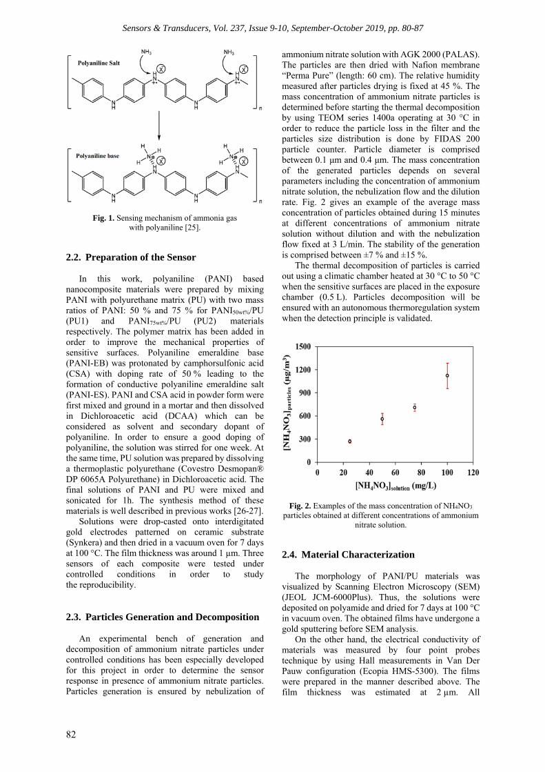
Sensors & Transducers, Vol. 237, Issue 9-10, September-October 2019, pp. 80-87
82
Fig. 1. Sensing mechanism of ammonia gas with polyaniline [25].
2.2. Preparation of the Sensor
In this work, polyaniline (PANI) based nanocomposite materials were prepared by mixing PANI with polyurethane matrix (PU) with two mass ratios of PANI: 50 % and 75 % for PANI50wt%/PU (PU1) and PANI75wt%/PU (PU2) materials respectively. The polymer matrix has been added in order to improve the mechanical properties of sensitive surfaces. Polyaniline emeraldine base (PANI-EB) was protonated by camphorsulfonic acid (CSA) with doping rate of 50 % leading to the formation of conductive polyaniline emeraldine salt (PANI-ES). PANI and CSA acid in powder form were first mixed and ground in a mortar and then dissolved in Dichloroacetic acid (DCAA) which can be considered as solvent and secondary dopant of polyaniline. In order to ensure a good doping of polyaniline, the solution was stirred for one week. At the same time, PU solution was prepared by dissolving a thermoplastic polyurethane (Covestro Desmopan® DP 6065A Polyurethane) in Dichloroacetic acid. The final solutions of PANI and PU were mixed and sonicated for 1h. The synthesis method of these materials is well described in previous works [26-27].
Solutions were drop-casted onto interdigitated gold electrodes patterned on ceramic substrate (Synkera) and then dried in a vacuum oven for 7 days at 100 °C. The film thickness was around 1 µm. Three sensors of each composite were tested under controlled conditions in order to study the reproducibility.
2.3. Particles Generation and Decomposition
An experimental bench of generation and decomposition of ammonium nitrate particles under controlled conditions has been especially developed for this project in order to determine the sensor response in presence of ammonium nitrate particles. Particles generation is ensured by nebulization of
ammonium nitrate solution with AGK 2000 (PALAS). The particles are then dried with Nafion membrane “Perma Pure” (length: 60 cm). The relative humidity measured after particles drying is fixed at 45 %. The mass concentration of ammonium nitrate particles is determined before starting the thermal decomposition by using TEOM series 1400a operating at 30 °C in order to reduce the particle loss in the filter and the particles size distribution is done by FIDAS 200 particle counter. Particle diameter is comprised between 0.1 μm and 0.4 μm. The mass concentration of the generated particles depends on several parameters including the concentration of ammonium nitrate solution, the nebulization flow and the dilution rate. Fig. 2 gives an example of the average mass concentration of particles obtained during 15 minutes at different concentrations of ammonium nitrate solution without dilution and with the nebulization flow fixed at 3 L/min. The stability of the generation is comprised between ±7 % and ±15 %.
The thermal decomposition of particles is carried out using a climatic chamber heated at 30 °C to 50 °C when the sensitive surfaces are placed in the exposure chamber (0.5 L). Particles decomposition will be ensured with an autonomous thermoregulation system when the detection principle is validated.
Fig. 2. Examples of the mass concentration of NH4NO3
particles obtained at different concentrations of ammonium nitrate solution.
2.4. Material Characterization
The morphology of PANI/PU materials was visualized by Scanning Electron Microscopy (SEM) (JEOL JCM-6000Plus). Thus, the solutions were deposited on polyamide and dried for 7 days at 100 °C in vacuum oven. The obtained films have undergone a gold sputtering before SEM analysis.
On the other hand, the electrical conductivity of materials was measured by four point probes technique by using Hall measurements in Van Der Pauw configuration (Ecopia HMS-5300). The films were prepared in the manner described above. The film thickness was estimated at 2 µm. All
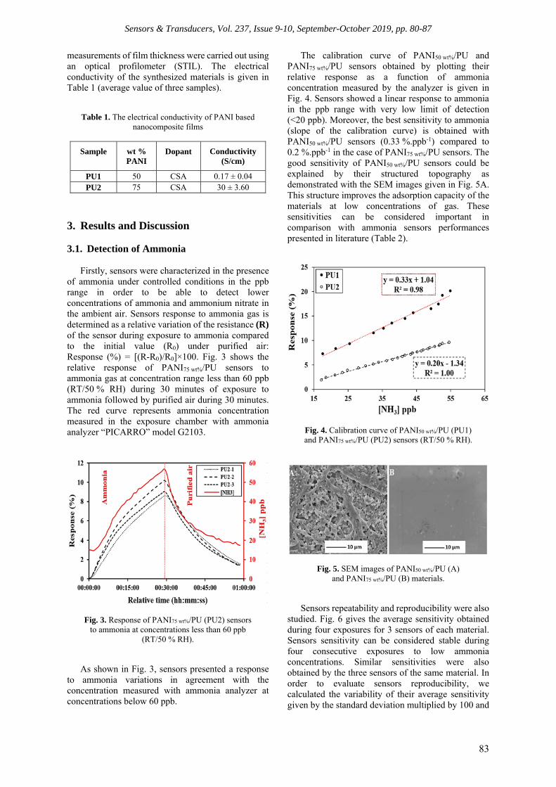
Sensors & Transducers, Vol. 237, Issue 9-10, September-October 2019, pp. 80-87
83
measurements of film thickness were carried out using an optical profilometer (STIL). The electrical conductivity of the synthesized materials is given in Table 1 (average value of three samples).
Table 1. The electrical conductivity of PANI based nanocomposite films
Sample wt % PANI
Dopant Conductivity (S/cm)
PU1 50 CSA 0.17 ± 0.04 PU2 75 CSA 30 ± 3.60
3. Results and Discussion 3.1. Detection of Ammonia
Firstly, sensors were characterized in the presence of ammonia under controlled conditions in the ppb range in order to be able to detect lower concentrations of ammonia and ammonium nitrate in the ambient air. Sensors response to ammonia gas is determined as a relative variation of the resistance (R) of the sensor during exposure to ammonia compared to the initial value (R0) under purified air: Response (%) = [(R-R0)/R0]×100. Fig. 3 shows the relative response of PANI75 wt%/PU sensors to ammonia gas at concentration range less than 60 ppb (RT/50 % RH) during 30 minutes of exposure to ammonia followed by purified air during 30 minutes. The red curve represents ammonia concentration measured in the exposure chamber with ammonia analyzer “PICARRO” model G2103.
Fig. 3. Response of PANI75 wt%/PU (PU2) sensors to ammonia at concentrations less than 60 ppb
(RT/50 % RH).
As shown in Fig. 3, sensors presented a response to ammonia variations in agreement with the concentration measured with ammonia analyzer at concentrations below 60 ppb.
The calibration curve of PANI50 wt%/PU and PANI75 wt%/PU sensors obtained by plotting their relative response as a function of ammonia concentration measured by the analyzer is given in Fig. 4. Sensors showed a linear response to ammonia in the ppb range with very low limit of detection (<20 ppb). Moreover, the best sensitivity to ammonia (slope of the calibration curve) is obtained with PANI50 wt%/PU sensors (0.33 %.ppb-1) compared to 0.2 %.ppb-1 in the case of PANI75 wt%/PU sensors. The good sensitivity of PANI50 wt%/PU sensors could be explained by their structured topography as demonstrated with the SEM images given in Fig. 5A. This structure improves the adsorption capacity of the materials at low concentrations of gas. These sensitivities can be considered important in comparison with ammonia sensors performances presented in literature (Table 2).
Fig. 4. Calibration curve of PANI50 wt%/PU (PU1) and PANI75 wt%/PU (PU2) sensors (RT/50 % RH).
Fig. 5. SEM images of PANI50 wt%/PU (A) and PANI75 wt%/PU (B) materials.
Sensors repeatability and reproducibility were also studied. Fig. 6 gives the average sensitivity obtained during four exposures for 3 sensors of each material. Sensors sensitivity can be considered stable during four consecutive exposures to low ammonia concentrations. Similar sensitivities were also obtained by the three sensors of the same material. In order to evaluate sensors reproducibility, we calculated the variability of their average sensitivity given by the standard deviation multiplied by 100 and
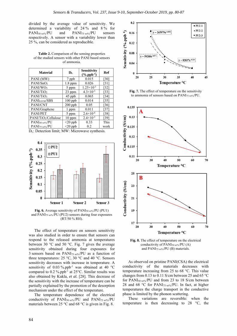
Sensors & Transducers, Vol. 237, Issue 9-10, September-October 2019, pp. 80-87
84
divided by the average value of sensitivity. We determined a variability of 24 % and 8 % for PANI50 wt%/PU and PANI75 wt%/PU sensors respectively. A sensor with a variability lower than 25 %, can be considered as reproducible.
Table 2. Comparison of the sensing properties of the studied sensors with other PANI based sensors
of ammonia.
Material DL Sensitivity (%.ppb-1) Ref
PANI (MW) 7 ppb 0.015 [30]PANI/SnO2 1.8 ppm 0.026 [31]PANI/WO3 5 ppm 1.25×10⁻³ [32]PANI/TiO2 23 ppm 4.3×10⁻³ [33]PANI/TiO2 45 ppb 0.065 [34]PANI0.01M/SBS 100 ppb 0.014 [35]PANI/CNT 200 ppb 0.05 [36] PANI/Graphene 1 ppm 0.011 [37] PANI/PET 5 ppm 2.6×10⁻⁴ [38]
PANI/TiO2/Cellulose 10 ppm 2.4×10⁻³ [39] PANI50 wt%/PU PANI75 wt%/PU
<20 ppb <20 ppb
0.33 0.2
This work
DL: Detection limit; MW: Microwave synthesis.
Fig. 6. Average sensitivity of PANI50 wt%/PU (PU1) and PANI75 wt%/PU (PU2) sensors during four exposures
(RT/50 % RH).
The effect of temperature on sensors sensitivity was also studied in order to ensure that sensors can respond to the released ammonia at temperatures between 30 °C and 50 °C. Fig. 7 gives the average sensitivity obtained during four exposures for 3 sensors based on PANI75 wt%/PU as a function of three temperatures: 25 °C, 30 °C and 40 °C. Sensors sensitivity decreases with increase in temperature. A sensitivity of 0.03 %.ppb-1 was obtained at 40 °C compared to 0.2 %.ppb-1 at 25°C. Similar results was also obtained by Kukla, et al. [28]. This decrease of the sensitivity with the increase of temperature can be partially explained by the promotion of the desorption mechanism under the effect of the temperature.
The temperature dependence of the electrical conductivity of PANI50 wt%/PU and PANI75 wt%/PU materials between 25 °C and 68 °C is given in Fig. 8.
Fig. 7. The effect of temperature on the sensitivity to ammonia of sensors based on PANI75 wt%/PU.
Fig. 8. The effect of temperature on the electrical conductivity of PANI50 wt%/PU (A) and PANI75 wt%/PU (B) materials.
As observed on pristine PANI(CSA) the electrical conductivity of the materials decreases with temperature increasing from 25 to 68 °C. This value changes from 0.13 to 0.11 S/cm between 25 and 65 °C for PANI50 wt%/PU and from 23 to 18 S/cm between 28 and 68 °C for PANI75 wt%/PU. In fact, at higher temperatures the charge transport in the conductive phase is limited by the phonon scattering.
These variations are reversible: when the temperature is then decreasing to 28 °C, the
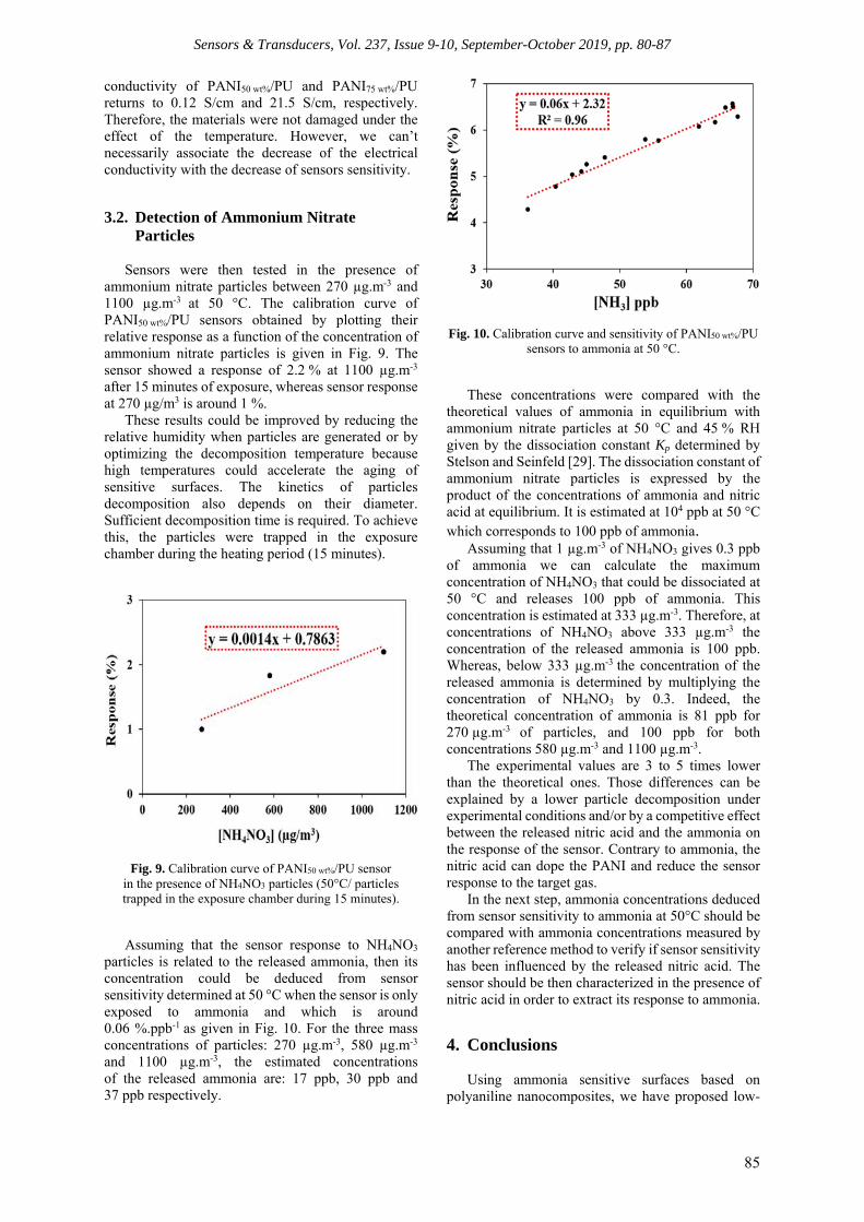
Sensors & Transducers, Vol. 237, Issue 9-10, September-October 2019, pp. 80-87
85
conductivity of PANI50 wt%/PU and PANI75 wt%/PU returns to 0.12 S/cm and 21.5 S/cm, respectively. Therefore, the materials were not damaged under the effect of the temperature. However, we can’t necessarily associate the decrease of the electrical conductivity with the decrease of sensors sensitivity.
3.2. Detection of Ammonium Nitrate Particles
Sensors were then tested in the presence of
ammonium nitrate particles between 270 µg.m-3 and 1100 µg.m-3 at 50 °C. The calibration curve of PANI50 wt%/PU sensors obtained by plotting their relative response as a function of the concentration of ammonium nitrate particles is given in Fig. 9. The sensor showed a response of 2.2 % at 1100 µg.m-3 after 15 minutes of exposure, whereas sensor response at 270 µg/m3 is around 1 %.
These results could be improved by reducing the relative humidity when particles are generated or by optimizing the decomposition temperature because high temperatures could accelerate the aging of sensitive surfaces. The kinetics of particles decomposition also depends on their diameter. Sufficient decomposition time is required. To achieve this, the particles were trapped in the exposure chamber during the heating period (15 minutes).
Fig. 9. Calibration curve of PANI50 wt%/PU sensor in the presence of NH4NO3 particles (50°C/ particles trapped in the exposure chamber during 15 minutes).
Assuming that the sensor response to NH4NO3 particles is related to the released ammonia, then its concentration could be deduced from sensor sensitivity determined at 50 °C when the sensor is only exposed to ammonia and which is around 0.06 %.ppb-1 as given in Fig. 10. For the three mass concentrations of particles: 270 µg.m-3, 580 µg.m-3 and 1100 µg.m-3, the estimated concentrations of the released ammonia are: 17 ppb, 30 ppb and 37 ppb respectively.
Fig. 10. Calibration curve and sensitivity of PANI50 wt%/PU sensors to ammonia at 50 °C.
These concentrations were compared with the theoretical values of ammonia in equilibrium with ammonium nitrate particles at 50 °C and 45 % RH given by the dissociation constant Kp determined by Stelson and Seinfeld [29]. The dissociation constant of ammonium nitrate particles is expressed by the product of the concentrations of ammonia and nitric acid at equilibrium. It is estimated at 104 ppb at 50 °C which corresponds to 100 ppb of ammonia.
Assuming that 1 µg.m-3 of NH4NO3 gives 0.3 ppb of ammonia we can calculate the maximum concentration of NH4NO3 that could be dissociated at 50 °C and releases 100 ppb of ammonia. This concentration is estimated at 333 µg.m-3. Therefore, at concentrations of NH4NO3 above 333 µg.m-3 the concentration of the released ammonia is 100 ppb. Whereas, below 333 µg.m-3 the concentration of the released ammonia is determined by multiplying the concentration of NH4NO3 by 0.3. Indeed, the theoretical concentration of ammonia is 81 ppb for 270 µg.m-3 of particles, and 100 ppb for both concentrations 580 µg.m-3 and 1100 µg.m-3.
The experimental values are 3 to 5 times lower than the theoretical ones. Those differences can be explained by a lower particle decomposition under experimental conditions and/or by a competitive effect between the released nitric acid and the ammonia on the response of the sensor. Contrary to ammonia, the nitric acid can dope the PANI and reduce the sensor response to the target gas.
In the next step, ammonia concentrations deduced from sensor sensitivity to ammonia at 50°C should be compared with ammonia concentrations measured by another reference method to verify if sensor sensitivity has been influenced by the released nitric acid. The sensor should be then characterized in the presence of nitric acid in order to extract its response to ammonia.
4. Conclusions
Using ammonia sensitive surfaces based on polyaniline nanocomposites, we have proposed low-

Sensors & Transducers, Vol. 237, Issue 9-10, September-October 2019, pp. 80-87
86
cost sensors for simultaneous and selective measurement of ammonium nitrate particles and its gaseous precursor ammonia. The sensitive surfaces were synthesized with polyaniline associated with polyurethane. The first results obtained in the presence of ammonia showed a good sensitivity of PANI/PU materials at concentrations less than 60 ppb (around 0.33 %.ppb-1) with limit of detection lower than 20 ppb. Moreover, good repeatability and reproducibility were obtained. PANI/PU sensors characterized in the presence of ammonium nitrate particles at 50 °C, were capable of measuring a concentration of ammonium nitrate particles as low as 270 µg.m-3 with a sensitivity of 0.0014 %.µg-1.m3. The ongoing work is focused on the characterization of PANI/PU materials at lower concentrations of NH4NO3 particles. Acknowledgements
The authors are thankful to ADEME (Agence de l’Environnement et de la Maîtrise de l’Energie) in France for supporting this project and co-financing the PhD thesis of Mr. Mohamed BOUKHENANE with Région Hauts-de-France. The authors acknowledge also the staff of “SENSORS laboratory” and CERI (Centre d’Enseignement, de Recherche et d’Innovation) Energy and Environment of Institut Mines-Télécom Lille Douai (France). References [1]. V. P. Aneja, J. P. Chauhan, J. T. Walker,
Characterization of atmospheric ammonia emissions from swine waste storage and treatment lagoons, J. Geophys. Res. Atmospheres, Vol. 105, Issue D9, 2000, pp. 11535–11545.
[2]. J. H. Seinfeld, S. N. Pandis, Atmospheric Chemistry and Physics: From Air Pollution to Climate Change, John Wiley & Sons, 2016.
[3]. K. W. Van Der Hoek, Estimating ammonia emission factors in Europe: Summary of the work of the UNECE ammonia expert panel, Atmos. Environ., Vol. 32, Issue 3, 1998, pp. 315–316.
[4]. A. Fangmeier, A. Hadwiger-Fangmeier, L. Van der Eerden, H.-J. Jäger, Effects of atmospheric ammonia on vegetation-A review, Environ. Pollut., Vol. 86, Issue 1, 1994, pp. 43–82.
[5]. X. Tang, X. Zhang, Z. Ci, J. Guo, J. Wang, Speciation of the major inorganic salts in atmospheric aerosols of Beijing, China: Measurements and comparison with model, Atmos. Environ., Vol. 133, 2016, pp. 123–134.
[6]. T. Li, R. Hu, Z. Chen, Q. Li, S. Huang, Z. Zhu, L.-F. Zhou, Fine particulate matter (PM2.5): The culprit for chronic lung diseases in China, Chronic Dis. Transl. Med., Vol. 4, Issue 3, 2018, pp. 176–186.
[7]. X. Querol, A. Alastuey, T. Moreno, M. M. Viana, S. Castillo, J. Pey, S. Rodríguez, B. Artiñano, P. Salvador, M. Sánchez, S. Garcia Dos Santos, M. D. Herce Garraleta, R. Fernandez-Patier, S. Moreno-Grau, L. Negral, M. C. Minguillón, E. Monfort, M. J. Sanz, R. Palomo-Marín, E. Pinilla-
Gil, E. Cuevas, J. de la Rosa, A. Sánchez de la Campa, Spatial and temporal variations in airborne particulate matter (PM10 and PM2.5) across Spain 1999–2005, Atmos. Environ., Vol. 42, Issue 17, 2008, pp. 3964–3979.
[8]. N. Amil, M. T. Latif, M. F. Khan, M. Mohamad, Seasonal variability of PM2.5 composition and sources in the Klang Valley urban-industrial environment, Atmospheric Chem. Phys., Vol. 16, Issue 8, 2016, pp. 5357–5381.
[9]. J. Hu, Y. Wang, Q. Ying, H. Zhang, Spatial and temporal variability of PM2.5 and PM10 over the North China Plain and the Yangtze River Delta, China, Atmos. Environ., Vol. 95, 2014, pp. 598–609.
[10]. D. Lv, Y. Chen, T. Zhu, T. Li, F. Shen, X. Li, Tariq Mehmood, The pollution characteristics of PM10 and PM2.5 during summer and winter in Beijing, Suning and Islamabad, Atmospheric Pollut. Res., Vol. 10, Issue 4, 2019, pp. 1159-1164.
[11]. Y. Wang, Y. Ma, Z. Lu, H. Ma, Y. Zhang, N. Liu, Y. Hong, X. Li, In situ measurement of atmospheric particles mass concentration in Anshan, in Proceedings of the IOP Conf. Ser. Earth Environ. Sci., Vol. 69, Issue 1, 2017, 012026.
[12]. S. K. Sharma, T. K. Mandal, Chemical composition of fine mode particulate matter (PM2.5) in an urban area of Delhi, India and its source apportionment, Urban Clim., Vol. 21, 2017, pp. 106–122.
[13]. J. Tao, L. Zhang, G. Engling, R. Zhang, Y. Yang, J. Cao, C. Zhu, Q. Wang, L. Luo, Chemical composition of PM2.5 in an urban environment in Chengdu, China: Importance of springtime dust storms and biomass burning, Atmospheric Res., Vol. 122, 2013, pp. 270–283.
[14]. L. He, H. Chen, J. Rangognio, A. Yahyaoui, P. Colin, J. Wang, V. Daële, A. Mellouki, Fine particles at a background site in Central France: Chemical compositions, seasonal variations and pollution events, Sci. Total Environ., Vol. 612, 2018, pp. 1159–1170.
[15]. D. Salameh, A. Detournay, J. Pey, N. Pérez, F. Liguori, D. Saraga, M.C. Bove, P. Brotto, F. Cassola, D. Massabò, A. Latella, S. Pillon, G. Formenton, S. Patti, A. Armengaud, D. Piga, J.L. Jaffrezo, J. Bartzis, E. Tolis, P. Prati, X. Querol, H. Wortham, N. Marchand, PM2.5 chemical composition in five European Mediterranean cities: A 1-year study, Atmospheric Res., Vol. 155, 2015, pp. 102–117.
[16]. H. Wang, X. Li, G. Shi, J. Cao, C. Li, F. Yang, Y. Ma, K. He, PM2.5 Chemical Compositions and Aerosol Optical Properties in Beijing during the Late Fall, Atmosphere, Vol. 6, Issue 2, 2015, pp. 164–182.
[17]. N. Jiang, S. Yin, Y. Guo, J. Li, P. Kang, R. Zhang, X. Tang, Characteristics of mass concentration, chemical composition, source apportionment of PM2.5 and PM10 and health risk assessment in the emerging megacity in China, Atmospheric Pollut. Res., Vol. 9, Issue 2, 2018, pp. 309–321.
[18]. A. W. Stelson, S. K. Friedlander, J. H. Seinfeld, A note on the equilibrium relationship between ammonia and nitric acid and particulate ammonium nitrate, Atmospheric Environ. 1967, Vol. 13, Issue 9, 1979, pp. 369–371.
[19]. C. B. Richardson, R. L. Hightower, Evaporation of ammonium nitrate particles, Atmospheric Environ. 1967, Vol. 21, Issue 4, 1987, pp. 971–975.
[20]. R. K. Pathak, W. S. Wu, T. Wang, Summertime PM2.5 ionic species in four major cities of China: nitrate

Sensors & Transducers, Vol. 237, Issue 9-10, September-October 2019, pp. 80-87
87
formation in an ammonia-deficient atmosphere, Atmos. Chem. Phys., Vol. 9, 2009, pp. 1711–1720.
[21]. Y. Tao, X. Ye, Z. Ma, Y. Xie, R. Wang, J. Chen, X. Yang, S. Jiang, Insights into different nitrate formation mechanisms from seasonal variations of secondary inorganic aerosols in Shanghai, Atmos. Environ., Vol. 145, 2016, pp. 1–9.
[22]. X. Zhang, P. H. McMurry, Evaporative losses of fine particulate nitrates during sampling, Atmospheric Environ. Part Gen. Top., Vol. 26, Issue 18, 1992, pp. 3305–3312.
[23]. D. H. Lowenthal, N. Kumar, PM2.5 Mass and Light Extinction Reconstruction in IMPROVE, J. Air Waste Manag. Assoc., Vol. 53, Issue 9, 2003, pp. 1109–1120.
[24]. F. M. Kelly, L. Meunier, C. Cochrane, V. Koncar, Polyaniline: Application as solid state electrochromic in a flexible textile display, Displays, Vol. 34, Issue 1, 2013, pp. 1–7.
[25]. S. Mikhaylov, N. Ogurtsov, Y. Noskov, N. Redon, P. Coddeville, J.-L. Wojkiewicz, A. Pud, Ammonia/amine electronic gas sensors based on hybrid polyaniline–TiO2 nanocomposites. The effects of titania and the surface active doping acid, RSC Adv., Vol. 5, Issue 26, 2015, pp. 20218–20226.
[26]. J. L. Wojkiewicz, V. N. Bliznyuk, S. Carquigny, N. Elkamchi, N. Redon, T. Lasri, A. A. Pud, S. Reynaud, Nanostructured polyaniline-based composites for ppb range ammonia sensing, Sens. Actuators B Chem., Vol. 160, Issue 1, 2011, pp. 1394–1403.
[27]. M. L. Boukhenane, N. Redon, J. L. Wojkiewicz, P. Coddeville, Polyaniline nanocomposites based sensor for simultaneous and selective measurement of ammonium nitrate aerosol and ammonia gas, in Proceedings of the 5th International Conference on Sensors Engineering and Electronics Instrumentation Advances (SEIA'19), Tenerife (Canary Islands), Spain, 25-27 September 2019, pp. 250–254.
[28]. A. L. Kukla, Y. M. Shirshov, S. A. Piletsky, Ammonia sensors based on sensitive polyaniline films, Sens. Actuators B Chem., Vol. 37, Issue 3, 1996, pp. 135–140.
[29]. A. W. Stelson, J. H. Seinfeld, Relative humidity and temperature dependence of the ammonium nitrate dissociation constant, Atmospheric Environ. 1967, Vol. 16, Issue 5, 1982, pp. 983–992.
[30]. T. Mérian, N. Redon, Z. Zujovic, D. Stanisavljev, J. L. Wojkiewicz, M. Gizdavic-Nikolaidis, Ultra
sensitive ammonia sensors based on microwave synthesized nanofibrillar polyanilines, Sens. Actuators B Chem., Vol. 203, 2014, pp. 626–634.
[31]. S. Bai, Y. Tian, M. Cui, J. Sun, Y. Tian, R. Luo, A. Chen, D. Li, Polyaniline@SnO2 heterojunction loading on flexible PET thin film for detection of NH3 at room temperature, Sens. Actuators B Chem., Vol. 226, 2016, pp. 540–547.
[32]. S. B. Kulkarni, Y. H. Navale, S. T. Navale, N. S. Ramgir, A. K. Debnath, S. C. Gadkari, S. K. Gupta, D. K. Aswal, V. B. Patil, Enhanced ammonia sensing characteristics of tungsten oxide decorated polyaniline hybrid nanocomposites, Org. Electron., Vol. 45, 2017, pp. 65–73.
[33]. H. Tai, Y. Jiang, G. Xie, J. Yu, X. Chen, Fabrication and gas sensitivity of polyaniline–titanium dioxide nanocomposite thin film, Sens. Actuators B Chem., Vol. 125, Issue 2, 2007, pp. 644–650.
[34]. Y. Li, H. Ban, H. Zhao, M. Yang, Facile preparation of a composite of TiO2 nanosheets and polyaniline and its gas sensing properties, RSC Adv., Vol. 5, Issue 129, 2015, pp. 106945–106952.
[35]. X. Wang, S. Meng, M. Tebyetekerwa, W. Weng, J. Pionteck, B. Sun, Z. Qin, M. Zhu, Nanostructured polyaniline/poly(styrene-butadiene-styrene) compo-site fiber for use as highly sensitive and flexible ammonia sensor, Synth. Met., Vol. 233, 2017, pp. 86–93.
[36]. L. Xue, W. Wang, Y. Guo, G. Liu, P. Wan, Flexible polyaniline/carbon nanotube nanocomposite film-based electronic gas sensors, Sens. Actuators B Chem., Vol. 244, 2017, pp. 47–53.
[37]. Z. Wu, X. Chen, S. Zhu, Z. Zhou, Y. Yao, W. Quan, B. Liu, Enhanced sensitivity of ammonia sensor using graphene/polyaniline nanocomposite, Sens. Actuators B Chem., Vol. 178, 2013, pp. 485–493.
[38]. D. K. Bandgar, S. T. Navale, S. R. Nalage, R. S. Mane, F. J. Stadler, D. K. Aswal, S. K. Gupta, V. B. Patil, Simple and low-temperature polyaniline-based flexible ammonia sensor: a step towards laboratory synthesis to economical device design, J. Mater. Chem. C., Vol. 3, Issue 36, 2015, pp. 9461–9468.
[39]. Z. Pang, Z. Yang, Y. Chen, J. Zhang, Q. Wang, F. Huang, Q. Wei, A room temperature ammonia gas sensor based on cellulose/TiO2/PANI composite nanofibers, Colloids Surf. Physicochem. Eng. Asp., Vol. 494, 2016, pp. 248–255.
__________________
Published by International Frequency Sensor Association (IFSA) Publishing, S. L., 2019 (http://www.sensorsportal.com).
Sensors & Transducers, Vol. 237, Issue 9-10, September-October 2019, pp. 88-94
88
Sensors & Transducers
Published by IFSA Publishing, S. L., 2019 http://www.sensorsportal.com
The Measurement of Blood Coagulation Process in Extracorporeal Circuit Using LED
Photoacoustic Imaging
1, * Takahiro WABE, 2 Ryo SUZUKI, 2 Kazuo MARUYAMA and 1 Yasutaka UCHIDA
1 Teikyo University of Science, 2-2-1 Senjyusakuagi, Adati-ku, Tokyo, Japan 2 Faculty of Pharma-Science, Teikyo University, 2-11-1 Kaga, Itabasi-ku, Tokyo, Japan
Tel.: + 8169101010, fax: + 8169103800 E-mail: [email protected]
Received: 30 August 2019 /Accepted: 27 September 2019 /Published: 30 November 2019 Abstract: Blood coagulation is measured by using a pressure sensor in a blood circuit, but it is not quick responsive because it is detected by pressure rise caused by coagulation. In this study, we have investigated a method to detect blood clotting at an early stage using photoacoustic imaging, which is thought to be more sensitive. The LED with a wavelength of 850 nm was used as a photoacoustic light source. An ultrasonic wave generated by thermal expansion of mouse blood sealed in a microtube was observed, and also many ripples were observed with time and the coagulation of blood progressed. It was also observed that the waveform considered to correspond to coagulation of blood broadens with time. It was found from the above that there is a possibility that the state of blood clotting can be observed from outside the circuit of the extracorporeal circulation device by using the LED as a light source. Keywords: Blood coagulation, Photoacoustic imaging, LED, The circuit of the extracorporeal circulation device, Coagulation process. 1. Introduction
When patients undergo extracorporeal blood circulation using methods such as purification therapy, percutaneous cardiopulmonary support, granular leukocyte apheresis, leukapheresis, or auxiliary artificial hearts, blood comes into contact with foreign matter. This contact is known to cause phenomena such as the destruction of blood cells, blood coagulation, fibrinolytic system enhancement, or complementary activities (thrombus formation) [1-3]. Various attempts have been made to prevent blood clotting, and prevention methods using anticoagulants (such as heparin) are now in mainstream use [4-7]. It
is known that interfacing negatively charged nonphysiological substances activates blood coagulation; a heparin coating is used in the extracorporeal circulation circuit to inhibit coagulation caused by the reaction between blood and foreign matter as it weakens this negative charge [8-9]. However, because heparin also acts as a foreign body, it is difficult to completely prevent blood from clotting on the surface of the circuit or in the dialyzer.
In extant extracorporeal circulation circuits, a pressure sensor is used for coagulation detection. This sensor reacts only when blood clotting causes clogs in the circuit or when the blood flow becomes difficult, both of which cause a rise in blood pressure. If the
http://www.sensorsportal.com/HTML/DIGEST/P_3115.htm

Sensors & Transducers, Vol. 237, Issue 9-10, September-October 2019, pp. 88-94
89
response is delayed, the blood will continue to clot, putting the patient’s health at risk. In addition, when blood coagulation is observed, the extracorporeal circulation circuit is changed to a new circuit. However, due to the irregularity of the response, the burden placed on healthcare professionals is also very large. Furthermore, the clogged circuit results in the patient's blood, which should have been returned to the patient's circulation, being discarded. However, if coagulation in the circuit can be detected in advance, it would be possible to carry out an early response to circuit blockage by reverse calculation.
Because of the importance of an early response, sensing blood coagulation as well as understanding the details of the process at an early stage is required. There are some published studies that have measured blood coagulation using a photoacoustic imaging technique that uses a laser [10-12]. Despite this, the measurement of the process of thrombus growth by blood coagulation has not yet been reported. In addition, a solid-state laser is only used as a light source in conventional photoacoustic imaging [13]. The conventional laser device was not suitable for use as the light source for this study due to its weight and size, considering that it was necessary to attach it to a blood circuit regularly to measure changes in the state of the blood. Compared with light emitting diodes (LEDs), a solid-state laser has a volume ratio 15000 times that of a conventional laser, with a power consumption 1000 times higher and a cost ratio of 10 times or more. Because of the benefits of the LED technology, photoacoustic imaging using LEDs or laser diodes (LDs) as light sources is much more suitable for monitoring blood properties in this way. An LD can emit at a specific wavelength and has a higher energy density than an LED; however, since a resonator structure is required, using an LD for measurement becomes expensive. Thus, we believed that an LED was the most suitable light source for measuring blood coagulation in this study. This paper presents a preliminary study to measure the process of blood coagulation in the extracorporeal circuit system, using a photoacoustic imaging method to measure the changes that occur during blood clotting. 2. Methods 2.1. Measuring Coagulation Process with
Photoacoustic Image of LED Light Source
The extracorporeal circuit includes an air trap to
prevent air contamination. In addition, a mesh filter is installed to prevent generated blood clots from reaching the inside of the body from the external circuit. The air trap and mesh filter are installed in the drip chamber. Fig. 1 and Fig. 2 show the overall layout of the system and the drip chamber, respectively. Blood flow in the drip chamber is almost stationary due to the presence of the air trap and mesh filter. The
blood drip chamber plays an important role in the generation of coagulated blood, as blood is more likely to coagulate when flow is slow, as is the case in this component of the extracorporeal circuit. The low flow rates provide an advantage, however, in that they allow for measurement by photoacoustic technology. In this experiment, in order to reproduce the environment of a drip chamber with a very slow flow rate, blood was measured in a microtube.
Fig. 1. Schematic diagram of the blood flow in the blood purification circuit.
Fig. 2. The drip chamber.
Fig. 3 shows the schematic of the experimental setup used in this study. Measurement of the blood coagulation process was explored using PreXionLED AcousticX (CYBERDYNE, INC.). Approximately 1.5 mL of blood was placed in the microtube, and care was taken to prevent air from entering into the microtube. Additionally, two LED arrays were attached to both sides of the conventional ultrasonic probe, fixed in the water at approximately 40° with a jig. The distance between the microtube and the ultrasonic probe with the LED was approximately 1 cm. For the setting of measuring equipment, we referred to previous research [14].
We referred to existing data for the light absorption of the liquid and the blood coagulation. [15] The light energy was approximately 200 μJ/pulse, whereas the wavelength was 850 nm.

Sensors & Transducers, Vol. 237, Issue 9-10, September-October 2019, pp. 88-94
90
Fig. 3. Schematic diagram of the experimental apparatus. There were two types of ultrasonic probes: 10 and
7 MHz. At 10 MHz, the distance resolution improved to some extent, but the depth sensitivity increased 4 to 5 times at 7 MHz. Thus, the 7-MHz ultrasonic probe frequency was chosen.
2.2. Confirmation of Blood Coagulation by Change in the Blood Volume
Blood coagulation process in the microtube was
observed under the same conditions as in 2-1. Activated clotting time (ACT) is an important factor that can be used as a strict control for the administration of anticoagulants to the extracorporeal circuit. The measurement principle is activating blood coagulation by mixing an activator with the blood. ACT represents the time taken for clot formation [16]. However, there is no way to measure the coagulation process required for this experiment. Therefore, the index indicating the solidification process is scheduled. A schematic diagram of the experiment is shown in Fig. 4. The experimental procedure was as follows.
1. Blood was added into the transparent plastic
microtube and incubated for a certain period. 2. A mesh filter was used to separate the liquid
and coagulated parts of the blood. 3. The liquid part of the blood was transferred
into a beaker, and the liquid weight was measured. As clotting progresses, it can be expected that the
weight of liquid blood will decrease.
3. Result
As shown in Fig. 5, the vicinity of the wall surface of the microtube, where blood coagulation reacts with the foreign material, was measured. The thick black line indicates the side wall of the microtube.
Fig. 4. The coagulation process and separation of liquid blood.
The lower side is the side in contact with the blood and the upper side is the underwater side, with an arrow showing the boundary between the two. The red arrow is the A-mode measurement point described in 3.1.
Fig. 5. Correlation of experimental apparatus schematic diagram and imaging chart.
3.1. Measurement of Photoacoustic Phenomena Using A-mode Ultrasonic Imaging
First, the photoacoustic phenomenon generated
from the microtube was measured with an ultrasonic probe to show the intensity of the phenomenon (A-mode). The vertical axis represents the magnitude of vibration due to the photoacoustic phenomenon, whereas the horizontal axis represents the distance from the ultrasonic probe. To measure the time course of the blood clotting process, the photoacoustic response of the blood was measured just after blood was injected into the microtube (Fig. 6 (a)) and at 2 (Fig. 6 (b)), 5 (Fig. 6 (c)), and 10 min (Fig. 6 (d)).

Sensors & Transducers, Vol. 237, Issue 9-10, September-October 2019, pp. 88-94
91
(a)
(b)
(с)
(d)
Fig. 6. Measurement of photoacoustic phenomena using ultrasonic images (A-mode): (a) just after blood injection
(0 min); (b) 2 min; (c) 5 min; and (d) 10 min.
3.2. Measurement of Photoacoustic Phenomena Using B-mode Ultrasonic Imaging
The ultrasonic probe is in the form of an array, and the location where the photoacoustic phenomenon occurs can be identified. Fig. 7 shows the state of the elastic wave inside the microtube by synthesizing the waveform of the A-mode wave observed along the tube’s longer axis. The measurement timing was the same as in Fig. 6. Fig. 7 is rotated 90° from the actual
state shown in Fig. 5 for the convenience of subsequent graphing. The microtube shown in Fig. 7 is vertically oriented so that the wall surface is on the left side. As time elapsed, the number of white parabolic streaks increased on the side of the microtube in contact with the blood. The white part (high brightness) of the image represents the elastic wave from the absorber obtaining light energy.
Fig. 7. Photograph by photoacoustic imaging: (a) just after blood injection (0 min); (b) 2 min; (c) 5 min;
and (d) 10 min.
The pixel luminance of Fig. 7 is shown in Fig. 8 as a 3D color scale graph+ converted by free software (ImageJ) [17-18].
The x-axis represents the horizontal distance (5 mm), the y-axis represents the vertical distance (12 mm), and the z-axis is the value obtained by calculating the pixel luminance (256 scales).
It was unclear whether the origin of the photoacoustic phenomenon seen in Fig. 8 was the coagulation activity of the blood or not. Therefore, measurement was performed while blood coagulation in the tube was suppressed by introduction of heparin. Heparin was added to the blood and incubated for 10 min before measurement, in the same manner as the coagulated blood test in Fig. 8d. The results of this test are shown in Fig. 9. 3.3. Confirmation of Blood Coagulation
by Change in the Blood Volume
The blood volume passed through the mesh filter was found to decrease as time elapsed, dropping down to 79% after 10 min, as indicated in Table 1.
Table 1. Confirmation of blood coagulation process in microtube.
Elapsed time after injection of blood
into the microtube (min)
Blood volume passed through the mesh filter
(mL) 0 1.35 2 1.30 5 1.25
10 1.07

Sensors & Transducers, Vol. 237, Issue 9-10, September-October 2019, pp. 88-94
92
(a)
(b)
(c)
(d)
Fig. 8. 3D diagram of luminance part by ImageJ: (a) just after blood injection (0 min); (b) 2 min; (c) 5 min; and (d) 10 min.
(a)
(b)
Fig. 9. Photoacoustic imaging of heparinized coagulation inhibition: (a) Photograph; (b) Image; 3D diagram of luminance.

Sensors & Transducers, Vol. 237, Issue 9-10, September-October 2019, pp. 88-94
93
4. Discussion
In this study, changes in blood coagulation through contact with transparent plastics were measured by using photoacoustic methods. As shown in Fig. 7, it can be seen that ripples (indicated by white streaks) were generated from the center of the microtube, moving out toward the walls. The blood coagulation process was found to occur at the side of the tube in contact with blood, whereas no change was observed in the water outside the microtube. Additionally, in all measurements, as the light energy value irradiated to the microtube did not change, the elastic wave increased. Fig. 8 shows that the luminance of the blood portion of the microtube increased with time, indicating that blood coagulation was increasing from the inner wall of the microtube where the foreign matter reacted with the blood. Fig. 9 does not show the same elastic wave because of the inhibition of coagulation by heparin; the changes in photoacoustics over time do not occur in blood which does not coagulate. Fig. 7 shows that the elastic waves are generated inside the whole microtube, and that they grow over time. The results of the photoacoustic tests were found to correlate with the change in blood flow volume observed.
5. Conclusion
In this study, it was difficult to measure each the blood clot that formed in the microtube as was originally intended. However, the photoacoustic imaging using an LED light source confirmed the temporal change of blood coagulation in the microtube. Thus, it is possible to measure the temporal change of the blood coagulation process generated in an extracorporeal circuit using photoacoustic imaging with an LED light source. The optimization of wavelength energy and ultrasonic probe frequency in order to better measure blood coagulation through blood circuits should be studied further.
Acknowledgments
T. Wabe and Y. Uchida would like to thank Mr. N. Sato of CYBERDYNE, INC Research and Development Dept, for his cooperation in this experiment.
References [1]. J. Utley, Pathophysiology of cardiopulmonary bypass:
current issues, J Card Surg, Vol. 5, Issue 3, 1990, pp. 177-189.
[2]. Y. Mori, Haemocompatible Materials, Kobunshi Ronbunshu, Vol. 42, Issue 10, Oct. 1985, pp. 601-615. (in Japanese).
[3]. J. K. Kirklin, A. D. Pacifico, Complement and the damaging effects of cardiopulmonary bypass,
J. Thorac Cardiovasc Surg, Vol. 86, Issue 6, 1983, pp. 845-857.
[4]. L. Gott, J. D. Whiffen, R. C. Dutton, Heparin bonding on colloidal graphite surfaces, Science, Vol. 142, Issue 3597, 1963, pp. 1297-1298.
[5]. I. O. Salyer, Medical Application of Plasticю Biomedical Material Symposium, No. 1, Interscience, New York, 105, 1971.
[6]. M. Murase, A. Usui, M. Maeda, Y. Tomita, F. Murakami, K. Teranishi, T. Koyama, T. Ito, Ot. Abe, Nafamostat mesilate reduces blood loss during open heart surgery, Circulation, Vol. 88, Issue 5 Pt2, November 1993, pp. 11432-11436.
[7]. M. Hiroura, A. Usui, M. Kawamura, M. Hibi, K. Yoshida, F. Murakami, J. Iwase, Nafamostat mesilate reduces bloodcell adhesion to cardiopulmonary bypass circuit: an invitro study, J Extra Corpor Technol, Vol. 26, Issue 3, September 1994, pp. 121-125.
[8]. Segesser L. K., Weiss B. M., Garcia E., Felten A, Turina M. L., Reduction and elimination of systemic heparinization during cardiopulmonary bypass, J Thorac Cardiovasc Surg, Vol. 103, Issue 4, 1992, pp. 790-798.
[9]. Videm V., Molines T. E., Garred P., Svennevig J. L., Biocompatibility of extracorporeal circulation. In vitro comparison of heparin-coated and unmatedoxygenator circuits, J Thorac Cardiovasc Surg, Vol. 101, Issue 4, 1991, pp. 654-660.
[10]. Hongtao Zhong, Tingyang Duan, Hengrong Lan, Meng Zhou, Fei Gao, Review of low-cost photoacoustic sensing and imaging based on laser diode and light-emitting diode, Sensors, Vol. 18, Issue 7, 2018, p. 2264.
[11]. Thomas J. Allen, Paul C. Beard, High power visible light emitting diodes as pulsed excitation sources for biomedical photoacoustics, Biomedical Optics Express, Vol. 7, Issue 4, 2016, pp. 1260-1270.
[12]. Karpiouk A. B., Aglyamov S. R., Mallidi S., Shah J., Scott W. G., Rubin J. M., Emelianob S. Y., Combined ultrasound and photoacoustic imaging to detect and stage deep vein thrombosis. phantom and ex vivo studies, J Biomed Opt., Vol. 13, Issue 5, September-October 2008, 054061.
[13]. Bing Li, Cong Fu, Genshan Ma, Quli Fan, Yuyu Yao, Photoacoustic Imaging: A Novel for Detecting Carotid Artery Thrombosis in Mice, Journal of Vascular Research, Vol. 54, 2017, pp. 217-225.
[14]. Takahiro Wabe, Ryo Suzuki, Kazuo Maruyama, Yasutaka Uchida, Possibility for temporal observation of thrombus generated in extracorporeal circulator circuit by photoacoustic imaging using LED, in Proceedings of the 5th International Conference on Sensors Engineering and Electronics Instrumentation Advances (SEIA'19), Canary Islands (Tenerife), Spain, 25-27 September 2019, pp. 157-160.
[15]. Robert J. Talbert, Scott H. Holan, John A. Viator, Photoacoustic discrimination of viable and thermally coagulated blood using a two-wavelength method for burn injury monitoring, Physics in Medicine and Biology, Vol. 52, Issue 7, 2007, pp. 1815–1829.
[16]. Lee Roger I., White Paul D., A clinical study of the coagulation time of blood, The American Journal of the Medical Sciences, Vol. 145, April 1913, pp. 495-503.
[17]. Schneider C. A., Rasband W. S., Eliceiri K. W., NIH Image to ImageJ, 25 years of image analysis, Nature Methods, Vol. 9, Issue 7, 2012, pp. 671-675.

Sensors & Transducers, Vol. 237, Issue 9-10, September-October 2019, pp. 88-94
94
[18]. Abramoff M. D., Magalhaes P. J., Ram S. J., Image Processing with ImageJ, Biophotonics International, Vol. 11, Issue 7, 2004, pp. 36-42.
__________________
Published by International Frequency Sensor Association (IFSA) Publishing, S. L., 2019 (http://www.sensorsportal.com).

Sensors & Transducers, Vol. 237, Issue 9-10, September-October 2019, pp. 95-102
95
Sensors & Transducers
Published by IFSA Publishing, S. L., 2019 http://www.sensorsportal.com
Micro-calorimetric Flow Rate Measurement Device for Microfluidic Applications
Bilel Neji
College of Engineering and Technology, American University of the Middle East, Kuwait Tel.: +965 22251400, fax: +965 26548484
E-mail: [email protected]
Received: 30 August 2019 /Accepted: 27 September 2019 /Published: 30 November 2019 Abstract: With the recent advances in biology and medical fields, nano and micro sensors became essential for accurate measurements and diagnosis. Miniaturization of such critical devices has become essential to operate in micro scale circuits, including microfluidic devices that can be used for applications including preclinical diagnosis, drug monitoring and delivery, and lab on chip devices. Several techniques have been used to measure fluid flow rate. These techniques can be classified as thermal and non-thermal. This research focuses on calorimetric flow rate sensors, which is a sub-type of thermal flow rate sensors. This paper presents the design, microfabrication and characterization of a micro-calorimetric flow rate sensor. The device is capable of measuring fluid flow rates starting between 10 / and1 / . The sensing part of the device, excluding the power supply, measures 1 by4 . The channel width and height are both equal to100 . Experiment results show that measured output voltages ranging from 0.1 to0.28 , correspond to flow rates between 100 / and700 / . The device flow rate measurement error is around2 / , and the device response time is less than 3 seconds. Keywords: Micro-calorimetric measurement, Microfluidics, Fluid flow rate, Heat transfer, Temperature sensing, Microfabrication. 1. Introduction
Flow rate sensors have been widely used in biomedical engineering and research development. Flow rate sensors are key components used in a wide range of applications, including drug delivery, blood flow monitoring, and Lab on a Chip devices [1-4]. Several techniques have been used to measure fluid flow rate. These techniques can be classified as thermal and non-thermal. Non-thermal techniques include mechanical flow sensors and Coriolis mass flow meters. Mechanical flow sensors are considered as one of the most important groups of non-thermal flow measurement techniques. Fluid flow is usually laminar in microfluidics channels. Therefore,
calculation rules of drag force on the channel walls and the pressure drop in the direction of the fluid flow are known. Both drag and pressure drop are directly proportional to the velocity of the fluid flow. The authors in [5] stated that using piezo-resistive transducers and/or integrated pressure sensors, the flow velocity can be deduced and thus the flow rate in the sensor can be determined. On the other hand, the use of mass flow meters in microfluidics is growing as the technology is getting improved for microscale flows. In a mass flow meter operating on the “Coriolis principle”, the fluid flows on a vibrating channel. The Coriolis force acting on the moving fluid will affect the frequency, phase shift or amplitude of the initial vibration proportionally to the mass flow rate. The
http://www.sensorsportal.com/HTML/DIGEST/P_3116.htm
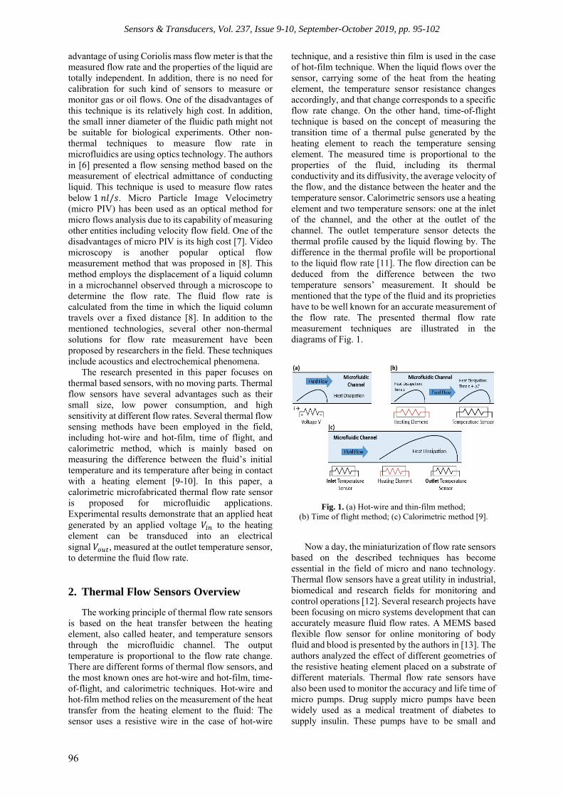
Sensors & Transducers, Vol. 237, Issue 9-10, September-October 2019, pp. 95-102
96
advantage of using Coriolis mass flow meter is that the measured flow rate and the properties of the liquid are totally independent. In addition, there is no need for calibration for such kind of sensors to measure or monitor gas or oil flows. One of the disadvantages of this technique is its relatively high cost. In addition, the small inner diameter of the fluidic path might not be suitable for biological experiments. Other non-thermal techniques to measure flow rate in microfluidics are using optics technology. The authors in [6] presented a flow sensing method based on the measurement of electrical admittance of conducting liquid. This technique is used to measure flow rates below1 / . Micro Particle Image Velocimetry (micro PIV) has been used as an optical method for micro flows analysis due to its capability of measuring other entities including velocity flow field. One of the disadvantages of micro PIV is its high cost [7]. Video microscopy is another popular optical flow measurement method that was proposed in [8]. This method employs the displacement of a liquid column in a microchannel observed through a microscope to determine the flow rate. The fluid flow rate is calculated from the time in which the liquid column travels over a fixed distance [8]. In addition to the mentioned technologies, several other non-thermal solutions for flow rate measurement have been proposed by researchers in the field. These techniques include acoustics and electrochemical phenomena.
The research presented in this paper focuses on thermal based sensors, with no moving parts. Thermal flow sensors have several advantages such as their small size, low power consumption, and high sensitivity at different flow rates. Several thermal flow sensing methods have been employed in the field, including hot-wire and hot-film, time of flight, and calorimetric method, which is mainly based on measuring the difference between the fluid’s initial temperature and its temperature after being in contact with a heating element [9-10]. In this paper, a calorimetric microfabricated thermal flow rate sensor is proposed for microfluidic applications. Experimental results demonstrate that an applied heat generated by an applied voltage to the heating element can be transduced into an electrical signal , measured at the outlet temperature sensor, to determine the fluid flow rate. 2. Thermal Flow Sensors Overview
The working principle of thermal flow rate sensors is based on the heat transfer between the heating element, also called heater, and temperature sensors through the microfluidic channel. The output temperature is proportional to the flow rate change. There are different forms of thermal flow sensors, and the most known ones are hot-wire and hot-film, time-of-flight, and calorimetric techniques. Hot-wire and hot-film method relies on the measurement of the heat transfer from the heating element to the fluid: The sensor uses a resistive wire in the case of hot-wire
technique, and a resistive thin film is used in the case of hot-film technique. When the liquid flows over the sensor, carrying some of the heat from the heating element, the temperature sensor resistance changes accordingly, and that change corresponds to a specific flow rate change. On the other hand, time-of-flight technique is based on the concept of measuring the transition time of a thermal pulse generated by the heating element to reach the temperature sensing element. The measured time is proportional to the properties of the fluid, including its thermal conductivity and its diffusivity, the average velocity of the flow, and the distance between the heater and the temperature sensor. Calorimetric sensors use a heating element and two temperature sensors: one at the inlet of the channel, and the other at the outlet of the channel. The outlet temperature sensor detects the thermal profile caused by the liquid flowing by. The difference in the thermal profile will be proportional to the liquid flow rate [11]. The flow direction can be deduced from the difference between the two temperature sensors’ measurement. It should be mentioned that the type of the fluid and its proprieties have to be well known for an accurate measurement of the flow rate. The presented thermal flow rate measurement techniques are illustrated in the diagrams of Fig. 1.
Fig. 1. (a) Hot-wire and thin-film method; (b) Time of flight method; (c) Calorimetric method [9].
Now a day, the miniaturization of flow rate sensors based on the described techniques has become essential in the field of micro and nano technology. Thermal flow sensors have a great utility in industrial, biomedical and research fields for monitoring and control operations [12]. Several research projects have been focusing on micro systems development that can accurately measure fluid flow rates. A MEMS based flexible flow sensor for online monitoring of body fluid and blood is presented by the authors in [13]. The authors analyzed the effect of different geometries of the resistive heating element placed on a substrate of different materials. Thermal flow rate sensors have also been used to monitor the accuracy and life time of micro pumps. Drug supply micro pumps have been widely used as a medical treatment of diabetes to supply insulin. These pumps have to be small and

Sensors & Transducers, Vol. 237, Issue 9-10, September-October 2019, pp. 95-102
97
accurate. The research in [14] presents an osmotic pressure pump, and a magnetic-driven pump, using miniaturized actuators based on a semi-permeable membrane and a magnet. In the recent years, with the research and technology advances, it became possible to fabricate complete systems combining a variety of micro sensors. PDMS (Polydimethylsiloxane) has been widely used to create microfluidic systems made of different modules that are either microfabricated using lithography and metal deposition, or using advanced 3D printing [15-16]. 3. Flow Rate Micro Sensor Design 3.1. Flow Rate Sensor Principle
The proposed thermal flow rate sensor uses the calorimetric technique at the micro scale. Energy cannot be created nor destroyed; it can only be converted from one form to the other. The designed sensor uses this concept to transduce an applied voltage into thermal energy, to be transferred to a fluid in contact with a heating element. The fluid will carry the heat and transfer it to the outlet temperature sensor. An inlet temperature sensor is used to determine the fluid’s initial temperature. Each measured temperature raise at a specific applied voltage will correspond to a specific flow rate of the fluid. A block diagram of the proposed flow rate sensor is shown in Fig. 2.
Fig. 2. Flow rate sensor block diagram.
The heating element is location between the two temperature sensors. 1corresponds to the fluid initial temperature before contacting the heating element, and 2 is the fluid’s temperature after being heated.
3.2. Sensor Simulation The simulation of the thermal flow rate sensor has
been performed using two different fluids: oil, and water. The proposed design of the thermal flow rate is shown in Fig. 3. Different structures with different dimension have been simulated.
Fig. 3. Proposed micro calorimeter design for simulation.
The simulation results confirm the working principle of the calorimetric method for flow rate sensing. This can be illustrated in Fig 4.
Fig. 4. Example of temperature profile of the heating element and the inlet & outlet sensors.
The simulation results in Table 1. Correspond to a heating element structure that has the following specifications: Thickness is1μ ; length is160μ , and width is400μ . The used flow rate is 1000μl/ and the applied power to the load is equal to100μ .
Table 1. Temperature variation between the input sensor and output sensor using oil then water as fluids.
Inlet
Sensor’s Outlet
Sensor’s (o )
Oil 352 366 14 Water 298 320 22
It can be concluded that water is better than oil for heat transferring from the heating element to the outlet temperature sensor. Water transfers almost double the amount of heat transferred by oil. Therefore, water will be used to simulate the real prototype.
3.3. Flow Rate Sensor Physical Design
The physical design of the microfabricated flow rate sensor is shown in Fig. 5(a). It consists of a microfluidic channel with a serpentine structure

Sensors & Transducers, Vol. 237, Issue 9-10, September-October 2019, pp. 95-102
98
bonded on the heating element to be used to transfer the heat to the fluid. PDMS is used to make the microfluidic channels. The heat is generated by the applied voltage , the equivalent of an applied power
. The heating element is a thin film made of tantalum nitride. Tantalum nitride has been chosen due to its low temperature coefficient of resistance (TCR). Low TCR is critical for the heating element to maintain uniform resistance in the large range of operating temperatures. The temperature sensors are made of platinum due to its linearity and relatively high TCR [17]. All metals and PDMS are deposited on a glass substrate. Glass has a very low thermal conductivity, which is 100 times smaller than that of silicon. Lower thermal conductivity is required to limit unwanted heat loss to the substrate and the surroundings. Fig. 5(b) presents a zoom-in of the microfluidic channel, the temperature sensors and the heating element. The heating element is shown in red; the microfluidic channel is in blue; and the inlet & outlet temperatures sensors and the coplanar waveguide, used to transfer the applied voltage to the heating element, are in grey.
Fig. 5. (a) Design of the proposed flow rate sensor; (b) Zoom-in of the designed heating element
and temperature sensors.
4. Thermal Flow Sensor Microfabrication 4.1. Fabrication Process
The proposed flow rate sensor is microfabricated in a 1000 class cleanroom environment.
Microchannel Fabrication:
In the process of microuidics fabrication, a mold is first produced. The mold is prepared on a silicon substrate and using the concept of photolithography to get the required design onto the mold. Then, soft lithography is employed to make the PDMS fluidic layer. The general procedures used in single-depth photolithography can be described In Fig. 6.
Since microfluidic devices work in small scale dimension, the surface contamination on the substrate must be cleaned to ensure perfect operation of the PDMS device. A 3-inch silicon wafer is first treated
with hydrofluoric acid for 5 minutes to remove its silicon dioxide layer. Then acetone, methanol and DI water are used one by one to remove the dirt particles on the surface. Lastly, after drying with nitrogen gas, the silicon wafer is ready for spin coating.
Fig. 6. General process for single-depth photolithography: (a) Substrate preparation; (b) Spin coating;
(c) UV exposure; (d) Development.
For microfluidic mold fabrication, a negative photoresist SU-8 is usually used for this purpose. Three different types of SU-8 were applied in our case. For the 35μ thickness lower layer, SU-8 2050 was placed on the substrate and then rotated at 4500 rpm for 30 seconds. The substrate is then placed on a hot plate for pre bake. The bake time is 1 minute for 65° and 5 minutes for95° . The purpose of pre bake is to evaporate excess coating solvent and harden the photoresist. UV exposure is a process of transferring pattern from the mask to photoresist. We can selectively remove parts of photoresist to get a desirable mold after its UV exposure under a predefined mask. For the negative photoresist SU-8, the area exposed to the UV light would become harder and insoluble within developer. Post bake is used to harden the photoresist. The wafer is baked at 65° for 1 minute and at 95° for 5 minutes. Lastly, the wafer is dipped into the SU-8 developer for 4-5 minutes. The part exposed to the UV light remains while the other part gets dissolved. Soft lithography refers to process that transferring pattern from SU-8 model to PDMS. PDMS is a moldable, biocompatible and optically transparent elastomeric polymer which has been widely used in microfluidic device fabrication. The process of soft lithography is shown in Fig. 7.
The SU-8 model is first treated with hexamethyldisilazane (HDMS), a release agent which works well for stripping of PDMS from the mold. Sylgard 184 silicone elastomer base and Sylgard 184 silicone elastomer curing agent are prepared for making PDMS. They are mixed with a ratio of 10:1.
Then the mixture is kept in the vacuum oven for degassing to get rid of air bubbles. The mixture is casted on the SU-8 model and cured at 60° until the PDMS is fully hardened. Lastly, the PDMS is peeled off from the SU-8 mold. Inlets and outlets are punched with blunt needle.
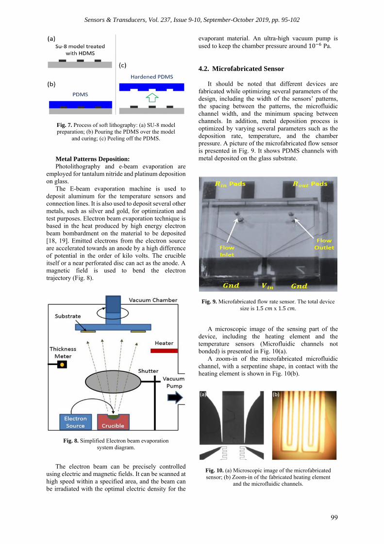
Sensors & Transducers, Vol. 237, Issue 9-10, September-October 2019, pp. 95-102
99
Fig. 7. Process of soft lithography: (a) SU-8 model preparation; (b) Pouring the PDMS over the model
and curing; (c) Peeling off the PDMS.
Metal Patterns Deposition: Photolithography and e-beam evaporation are
employed for tantalum nitride and platinum deposition on glass.
The E-beam evaporation machine is used to deposit aluminum for the temperature sensors and connection lines. It is also used to deposit several other metals, such as silver and gold, for optimization and test purposes. Electron beam evaporation technique is based in the heat produced by high energy electron beam bombardment on the material to be deposited [18, 19]. Emitted electrons from the electron source are accelerated towards an anode by a high difference of potential in the order of kilo volts. The crucible itself or a near perforated disc can act as the anode. A magnetic field is used to bend the electron trajectory (Fig. 8).
Fig. 8. Simplified Electron beam evaporation system diagram.
The electron beam can be precisely controlled using electric and magnetic fields. It can be scanned at high speed within a specified area, and the beam can be irradiated with the optimal electric density for the
evaporant material. An ultra-high vacuum pump is used to keep the chamber pressure around 10 Pa.
4.2. Microfabricated Sensor It should be noted that different devices are
fabricated while optimizing several parameters of the design, including the width of the sensors’ patterns, the spacing between the patterns, the microfluidic channel width, and the minimum spacing between channels. In addition, metal deposition process is optimized by varying several parameters such as the deposition rate, temperature, and the chamber pressure. A picture of the microfabricated flow sensor is presented in Fig. 9. It shows PDMS channels with metal deposited on the glass substrate.
Fig. 9. Microfabricated flow rate sensor. The total device size is 1.5 x 1.5 .
A microscopic image of the sensing part of the device, including the heating element and the temperature sensors (Microfluidic channels not bonded) is presented in Fig. 10(a).
A zoom-in of the microfabricated microfluidic channel, with a serpentine shape, in contact with the heating element is shown in Fig. 10(b).
Fig. 10. (a) Microscopic image of the microfabricated sensor; (b) Zoom-in of the fabricated heating element
and the microfluidic channels.

Sensors & Transducers, Vol. 237, Issue 9-10, September-October 2019, pp. 95-102
100
5. Experimental Results 5.1. Experiment Setup
Several equipment are used to determine the performance of the fabricated thermal flow rate sensor. The measurement setup is shown in Fig. 11(a).
Fig. 11. (a) DC measurement initial setup; (b) Probes setup for DC power measurement.
A "Fisher Scientific" mechanical syringe pump is used to pump the fluid in the micro channel. In addition, a nano volt meter, Agilent 34420A, is used to measure the output voltages of the temperature sensors. A Signatone probe station with six probes and a microscope is used to setup the connections between the device and the other equipment: two probes are used to apply DC power to the heating element, and four probes are used to measure the voltage across the temperature sensors. The applied DC power to the heating element is performed using a Tetronix ps2521 power supply. An applied power to the heating element will generate a heat that is transferred via the fluid to the outlet sensor, resulting in an increase in its resistance. Therefore, the sensor's output voltage increases accordingly. Deionized water is used for the experiment. The microfabricated flow sensor, while being tested on the probe station, is shown inside the blue circle of Fig. 11 (b).
5.2. Sensor Characterization
Several microfabricated devices are used for the characterization of the proposed flow sensor. The calorimetric principle is tested using one of the fabricated devices by measuring the sensor’s output voltage at a fixed 100 / flow rate, and an applied power , the equivalent of an applied voltage, to the heating element. The sensor’s response is around 0.9 when is 2 . When increasing the applied power to the heating element, increases accordingly as shown in Fig. 12. The sensor’s response increses to around 0.23 at an applied equal to 24 . It can be noted from the figure that the response time of the sensor while increasing the applied power to the heating element is in the order of 2 to 3 seconds.
Fig. 12. Temperature sensor output voltage vs. time at different applied powers at the heating element.
The optimization of the device’s power consumption is essential in order to increase the battery life time of the complete system. Therefore, it is very important to determine the value of the smallest typical amount of , whithout disturbing the function of the microfabricated device. Therefore, several experiments with different applied power to the heating element are conducted separately to define the typical value of to be used to operate the flow rate sensor.
The blue curve in the chart of Fig. 13 shows the applied voltage to the load over time. It is initially equal to 0 (14 if considering the offset voltage), 0.05 in average for the next minute, 0 for the next second minute, 0.05 for the next third minute, and 0 for the rest of the time.
On the other hand, the red curve represents the sensor's output voltage over time function of the applied voltage to the load, either 0 or 0.05 . Despite the relatively noisy output voltage at each applied voltage to the heating element, it can be noticed that the sensor's output voltage at an applied voltage of 0.05 can be relatively differentiated from the output voltage when 0 is applied to the heating element. Whithin the different experiments that are conducted using different applied voltages to the load, 0.05 applied voltage is considered the typical value that corresponds to the optimum power applied to the
(a)
(b)

Sensors & Transducers, Vol. 237, Issue 9-10, September-October 2019, pp. 95-102
101
heating element that can operate the fabricated flow rate sensor. That optimum power is around6 .
Fig. 13. Temperature sensor output voltage vs. applied voltage to the heating element.
The described experiment is conducted for different microfabricated devices to verify the consistence of the operation. Fig. 14 shows the results summary of two different devices, different from the device used for the results in Fig. 13. The blue diamonds represent the average of sensor's output voltage when no power is applied to the heating element,0 , and red squares represent the average of sensor's output voltage when 0.05 is applied to the heating element. It can be confirmed that there is a noticeable difference between the case where power is applied to the heating element and the case where no power is applied to the heating element, and this confirms the consistency of the device operation for an applied power 6 .
Fig. 14. Temperature sensor output voltage vs. applied voltage to the heating element using two different devices.
A set of microfabricated devices is tested to determine the relationship between the output voltage of the temperature sensor at the outlet and the fluid flow rate. It should be noted that each device has to be initially calibrated in order to be used in a complete system. Versus the flow rate is presented in the graph of Fig. 15.
Different applied powers to the heating element are experimented: 2.5 (black curve), 6 (orange curve), and 12 (blue curve). It can be concluded that the resolution of the sensor increases as the
applied power to the heating element is bigger. Results indicate that at a fixed applied voltage to the heating element, the flow rate increases, while less heat is being transferred to the output temperature sensor, and variation is reduced.
Fig. 15. Outlet temperature sensor voltage vs. fluid flow rate at different applied powers to the heating element.
Fluid flow rate measurement error has been calculated by fixing the fluid pump’s flow rate at different values, and then recording flow rate sensor readings over different periods of time. Fig. 16 and Fig. 17 present fluid flow rate sensor readings at fixed 400 μl/h and 500 μl/h, respectively.
Fig. 16. Measurement of a Fixed 400 μl/h Flow Rate over Time.
Fig. 17. Measurement of a Fixed 500 μl/h Flow Rate over Time.
Using data recorded over 12 minutes, the average reading error for a fixed flow rate of 400 /

Sensors & Transducers, Vol. 237, Issue 9-10, September-October 2019, pp. 95-102
102
is2.16 / , and the maximum reading error is5.92 / . Moreover, the average reading error for a fixed flow rate of 500 / is2.32 / , and the maximum reading error is 5.9 / . 5. Conclusions
A calorimetric microfabricated flow rate sensor is demonstrated. Experimental results show that an applied voltage to the heating element can generate heat that is transduced into an electrical signal to determine the corresponding flow rate of the fluid in use. In the future, the device will be tested in real life biomedical applications. This invasive approach will be much easier to install, use, and manipulate, compared to non-invasive methods such as ultrasound and Doppler measurement [20]. References [1]. Khan B., Ahmed S., Kakkar V., A Comparative
Analysis of Thermal Flow Sensing in Biomedical Applications, International journal of Biomedical Engineering and Science, Vol. 3, Issue 3, 2016, pp. 2016-3301.
[2]. Silvestri S., Schena E., Micromachined Flow Sensors in Biomedical Applications, Micromachines, 2012, Vol. 3, Issue 2, pp. 225-243.
[3]. Cerimovic S., Keplinger F., Beigelbeck R., Jachimowicz A., Antlinger H., Jakoby B., Monitoring the glycerol concentration in aqueous glycerol solutions using a micromachined flow sensor, in Proceedings of the Microelectronic Systems Symposium (MESS), 2014, pp. 1-6.
[4]. B. Neji, Microfabricated Thermal Flow Rate Sensor, in Proceedings of the 5th International Conference on Sensors and Electronic Instrumentation Advances (SEIA’ 2019), Tenerife (Canary Islands), Spain, 25-27 September 2019, pp. 63-68.
[5]. N. T. Nguyen, Micromachined flow sensors - a review, Flow Measurement and Instrumentation,Vol. 8, Issue 1, 1997, pp. 7-16.
[6]. J. Collins, A. P. Lee, Microfluidic flow transducer based on the measurement of electrical admittance, Lab on a Chip, 2004, Vol. 4, pp. 7-10.
[7]. N. T. Nguyen, S. T. Wereley, Fundamentals and Applications of Microfluidics, Artech House, Boston, 2006.
[8]. Z. Yang, R. Maeda, Automatic micro flow rate measurement using a modified computer mouse device, in Proceedings of the 1st Annual international IEEE-EMBS Special Topic Conference on Microtechnologies in Medicine & Biology, Lyon, France, 2000.
[9]. T. W. Kuo J., Yu L., Meng E., Micromachined Thermal Flow Sensors - A Review, Micromachines, Vol. 3, Issue 3, 2012, pp. 550-573.
[10]. Tyson J., Micro-thermal Flow-rate Detection for Lab on-a-chip Technologies, Lab on a Chip, 2018.
[11]. Neji B., Xu J., Titus A. H., Meltzer J., Micro-Fabricated DC Comparison Calorimeter for RF Power Measurement, Sensors, Vol. 14, Issue 11, 2014, pp. 20245-20261.
[12]. Shaun F., et al., On the co-integration of a thermo-resistive flow-rate sensor in a multi-parameter sensing chip for water network monitoring, in Proceedings of the 19th International Conference on Solid-State Sensors, Actuators and Microsystems (TRANSDUCERS), Kaohsiung, Taiwan, 2017.
[13]. Hayashida Y., et al., C208 Development of Micro pressure sensor for applying to MEMS blood-flow meter, in Proceedings of the JSME Conference on Frontiers in Bioengineering, Vol. 26, 2015, pp. 145-146.
[14]. Mukouyama Y., et al., PDMS balloon pump with a microfluidic regulator for the continuous drug supply in low flow rate, in Proceedings of the 28th IEEE International Conference on Micro Electro Mechanical Systems, Estoril, 2015, pp. 666-669.
[15]. C. M. B. Ho, S. H. Ng, K. H. H. Li, Y. Yoon, 3D printed microfluidics for biological applications, Lab on a Chip, Vol. 15, Issue 18, 2015, pp. 3627-3637.
[16]. A. K. Au, W. Huynh, L. F. Horowitz, A. Folch, 3D Printed Microfluidics, Angew. Chem. Int. Ed., Vol. 55, Issue 12, 2016, pp. 3862-3681.
[17]. Hamaguchi K., Tsuchiyama T., Matsushita J., Oxidation of Tantalum Nitride, Materials Science Forum, Vol. 761, 2013, pp. 125-129.
[18]. T. Chen, et al., Physical and optical properties of ZnO thin films grown by DC sputtering deposition, in Proceedings of the 9th International Conference on Solid State and Integrated Circuit Technology, Oct. 2008, 742-745.
[19]. M. H. S. Alrashdan, et al., Aluminum nitride thin film deposition using DC sputtering, in Proceedings of the IEEE International Conference on Semiconductor Electronics, Aug. 2014. 72-75.
[20]. Ma L., Liu J., Wang J., Study of the Accuracy of Ultrasonic Flowmeters for Liquid, AASRI Procedia, Vol. 3, 2012, pp. 14-20.
__________________
Published by International Frequency Sensor Association (IFSA) Publishing, S. L., 2019 (http://www.sensorsportal.com).
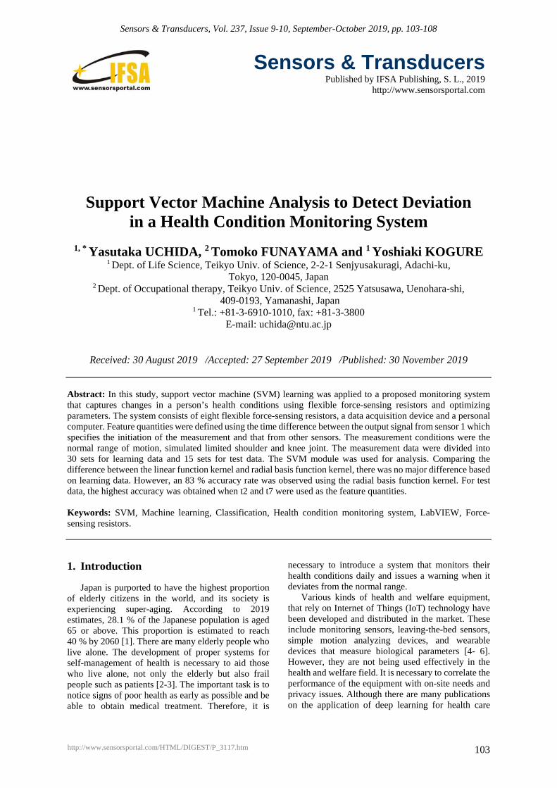
Sensors & Transducers, Vol. 237, Issue 9-10, September-October 2019, pp. 103-108
103
Sensors & Transducers
Published by IFSA Publishing, S. L., 2019 http://www.sensorsportal.com
Support Vector Machine Analysis to Detect Deviation in a Health Condition Monitoring System
1, * Yasutaka UCHIDA, 2 Tomoko FUNAYAMA and 1 Yoshiaki KOGURE
1 Dept. of Life Science, Teikyo Univ. of Science, 2-2-1 Senjyusakuragi, Adachi-ku, Tokyo, 120-0045, Japan
2 Dept. of Occupational therapy, Teikyo Univ. of Science, 2525 Yatsusawa, Uenohara-shi, 409-0193, Yamanashi, Japan
1 Tel.: +81-3-6910-1010, fax: +81-3-3800 E-mail: [email protected]
Received: 30 August 2019 /Accepted: 27 September 2019 /Published: 30 November 2019 Abstract: In this study, support vector machine (SVM) learning was applied to a proposed monitoring system that captures changes in a person’s health conditions using flexible force-sensing resistors and optimizing parameters. The system consists of eight flexible force-sensing resistors, a data acquisition device and a personal computer. Feature quantities were defined using the time difference between the output signal from sensor 1 which specifies the initiation of the measurement and that from other sensors. The measurement conditions were the normal range of motion, simulated limited shoulder and knee joint. The measurement data were divided into 30 sets for learning data and 15 sets for test data. The SVM module was used for analysis. Comparing the difference between the linear function kernel and radial basis function kernel, there was no major difference based on learning data. However, an 83 % accuracy rate was observed using the radial basis function kernel. For test data, the highest accuracy was obtained when t2 and t7 were used as the feature quantities. Keywords: SVM, Machine learning, Classification, Health condition monitoring system, LabVIEW, Force-sensing resistors.
1. Introduction Japan is purported to have the highest proportion
of elderly citizens in the world, and its society is experiencing super-aging. According to 2019 estimates, 28.1 % of the Japanese population is aged 65 or above. This proportion is estimated to reach 40 % by 2060 [1]. There are many elderly people who live alone. The development of proper systems for self-management of health is necessary to aid those who live alone, not only the elderly but also frail people such as patients [2-3]. The important task is to notice signs of poor health as early as possible and be able to obtain medical treatment. Therefore, it is
necessary to introduce a system that monitors their health conditions daily and issues a warning when it deviates from the normal range.
Various kinds of health and welfare equipment, that rely on Internet of Things (IoT) technology have been developed and distributed in the market. These include monitoring sensors, leaving-the-bed sensors, simple motion analyzing devices, and wearable devices that measure biological parameters [4- 6]. However, they are not being used effectively in the health and welfare field. It is necessary to correlate the performance of the equipment with on-site needs and privacy issues. Although there are many publications on the application of deep learning for health care
http://www.sensorsportal.com/HTML/DIGEST/P_3117.htm

Sensors & Transducers, Vol. 237, Issue 9-10, September-October 2019, pp. 103-108
104
monitoring, the field is still developing [7-8]. We have already proposed a physical condition monitoring system that uses force-sensing resistors is proposed [9-12]. In this paper, we have reported optimization on 3-class classification using support vector machine (SVM).
This research was conducted with the approval of the Teikyo University of Science’s Ethics Committee.
2. Experiment
2.1. Survey Method
The test subject was a man in his 60s. There were three measurement conditions: normal range of motion, simulated limited right knee, and right shoulder. In the classification result, the normal range of motion is represented by black circles, the simulated limited right knee is represented by green circles, limited right shoulder is represented by red circles. 2.2. Health Condition Monitoring System
and Data
The developed system consists of eight flexible force-sensing resistors (FSR®408) connected to a LabVIEW Data Acquisition (DAQ) NI-6210 device that is connected to a personal computer (PC) through a USB cable, as shown in Fig. 1. The voltage data were saved on the PC in a CSV file format. The first sensor was placed on the pillow and its output signal used the movement detection point as a reference. Three sensors were placed about 0.1 m apart at the edge of bed, and the remaining four sensors were placed about 0.2 m apart on the floor besides the bed [9]. A folding type bed was used in the experiment. The bed had a height of 0.4 m which is lower than a typical home bed. The second and subsequent sensors were located below the mat for protection. Thus, a very small output voltage was observed even when any weight was not added.
Fig. 2 shows details of the detecting circuit used in this experiment. The resistance value of the flexible force sensor changes in the range of 100 to 10 MΩ or more. Each flexible force-sensor was connected to a 1 kΩ resistor in series. The voltage drop across the 1kΩ resistor was used as the input voltage for the DAQ device. The sampling time was 10 ms, i.e., the output from each of the eight sensors was taken every 10 ms.
Fig. 3 shows the voltage output obtained from the DAQ. Each signal from the flexible force-sensors was smoothened by averaging adjacent data. The quantification of feature quantities for SVM analysis was defined by the time difference. The reference time was the fall time of sensor s1 on the pillow. The difference between the reference time and the rise time of other sensors’ (s2-s7) signals was defined as the response time, such as t2, t3, ...t7. For waveforms in which the rise time of the signal could
not be detected, the final 10 seconds were used as the rise time of the sensor.
Fig. 1. Health Condition Monitoring System.
Fig. 2. Details of the detecting circuit.
Fig. 3. Voltage output obtained by DAQ.
2.3. Analysis Method
The library for machine learning used scikit-learn, and the classification module used the SVM module. The measurement data were divided into two parts: 10 sets of data corresponding to 3 different conditions for learning data and 6 sets of data corresponding to 3 different conditions for test data. Five arbitrary sets were chosen from them to calculate the average value of accuracy rate.
The rise time of each sensor reflected the difference between the measurement conditions. A 2-D map of the rise time was used for comparison. Among the 2-D combinations, three combinations that are considered possible to classify were selected as feature quantities. Classification data used for the analysis were a combination of 2 kinds of 4 feature quantities with a high possibility of a high accuracy rate, because of comparing the selection of feature quantities of machine learning.
VCC
GND
sensor1
S1
S8
・・・・・・
VCC
GND
sensor8
GND
Data Logger
PC
0 5 10
Vout
[V]
Time [s]
t2
t4
t7
t6t5
t3

Sensors & Transducers, Vol. 237, Issue 9-10, September-October 2019, pp. 103-108
105
3. Results and Discussion
Fig. 4 (a), (b), (c) and (d) show the classification results using the pair t2 and t7 in the learning data. The kernels used in classification are linear kernel and radial basis function kernel using (C = 1.0, γ = 1E-6), (C = 1.0, γ = 1E-5) and (C = 10, γ = 1E-5). The unit value of t2 and t7 is 10 ms. For radial basis function, as the γ value increases, the boundary line changes from a straight line to a curve line and more accurate classification is achieved. The accuracy rate of classification obtained by linear and radial basis function kernel using (C = 1.0, γ = 1E-6), (C = 1.0, γ = 1E-5) and (C = 10.0, γ = 1E-5) applied to learning data are 80, 70, 80 and 80 %, respectively. After performing SVM learning using learning data, the 6 set of data for test were applied to the learning result to obtain an accuracy rate. The accuracy rates in the linear kernel and radial basis function kernel using (C = 1.0, γ = 1E-5), and (C = 10.0, γ = 1E-5) are 91.1, 86.7, 96.3 and 88.9 %, respectively.
The accuracy rate of radial function kernel was lower than that of linear function kernel. This result can be improved by optimizing C and γ parameters.
Fig. 5 (a), (b), (c) and (d) show classification results using the pair of t3 and t7 in the learning data and the kernel used for classifications which were linear kernel and radial basis function kernel using (C = 1.0, γ = 1E-6), (C = 1.0, γ = 1E-5) and (C = 1.0, γ = 0.5), respectively. The unit value of t3 and t7 is 10 ms. For radial basis function, as the γ value
increased, the boundary line changed from a straight line to curve line for more accurate classification.
The accuracy rate of classification obtained by linear and radial basis function kernel using (C = 1.0, γ = 1E-5) from learning data were 76.7 % and 56.6 %, respectively. After performing SVM learning using learning data, 6 sets of data for test were applied to the learning result to obtain an accuracy rate. The accuracy rates in the linear and radial basis function kernel (C = 1.0, γ = 1E-6) and (C = 10.0, γ = 1E-5) were 94.4, 84.4 and 100 %, respectively. For (C=10.0, γ =1E-5), the classification was over-fitting. The accuracy rate of classification obtained from radial function kernel was lower than that obtained from the linear function kernel. This result can be improved by optimizing parameters of C and γ.
Fig. 6 (a), (b), (c) and (d) shows classification results using the pair of t4 and t7 in the learning data. The kernel used in classifications were linear and radial basis function (C = 1.0, γ = 1E-6), (C = 1.0, γ = 1E-5) and (C = 50, γ = 1E-6), respectively. The unit value of t4 and t7 is 10 ms. The accuracy rates obtained using learning data, linear kernel, (C = 1.0, γ = 1E-6) and (C = 50.0, γ = 1E-6) are 83.3, 60.0, and 83.3 %, respectively. After performing SVM learning using data for learning, 15 test data are applied to the learning result to obtain an accuracy rate. The accuracy rates in the linear and radial basis function kernels (C=1.0 γ =1E-6) and (C=50.0, γ =1E-6) are 88.3, 60.0 and 83.3 %, respectively.
(a) Linear kernel (b) Radial basis function kernel. (C = 1.0, γ = 1E-6)
(c) Radial basis function kernel. (C = 1.0, γ = 1E-5)
(d) Radial basis function kernel. (C = 10, γ = 1E-5)
Fig. 4. Classification results for t2-t7.
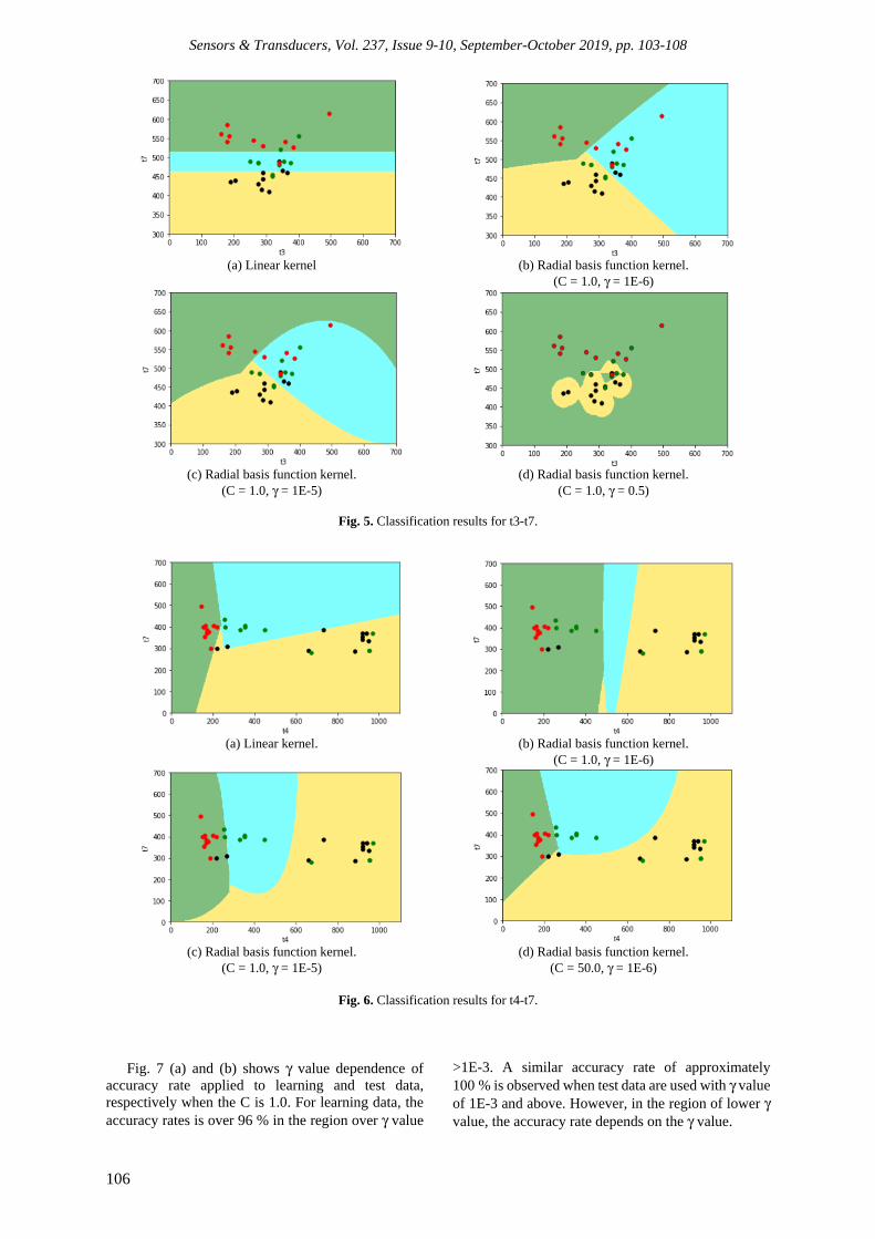
Sensors & Transducers, Vol. 237, Issue 9-10, September-October 2019, pp. 103-108
106
(a) Linear kernel (b) Radial basis function kernel. (C = 1.0, γ = 1E-6)
(c) Radial basis function kernel. (C = 1.0, γ = 1E-5)
(d) Radial basis function kernel. (C = 1.0, γ = 0.5)
Fig. 5. Classification results for t3-t7.
(a) Linear kernel. (b) Radial basis function kernel. (C = 1.0, γ = 1E-6)
(c) Radial basis function kernel. (C = 1.0, γ = 1E-5)
(d) Radial basis function kernel. (C = 50.0, γ = 1E-6)
Fig. 6. Classification results for t4-t7.
Fig. 7 (a) and (b) shows γ value dependence of
accuracy rate applied to learning and test data, respectively when the C is 1.0. For learning data, the accuracy rates is over 96 % in the region over γ value
>1E-3. A similar accuracy rate of approximately 100 % is observed when test data are used with γ value of 1E-3 and above. However, in the region of lower γ value, the accuracy rate depends on the γ value.
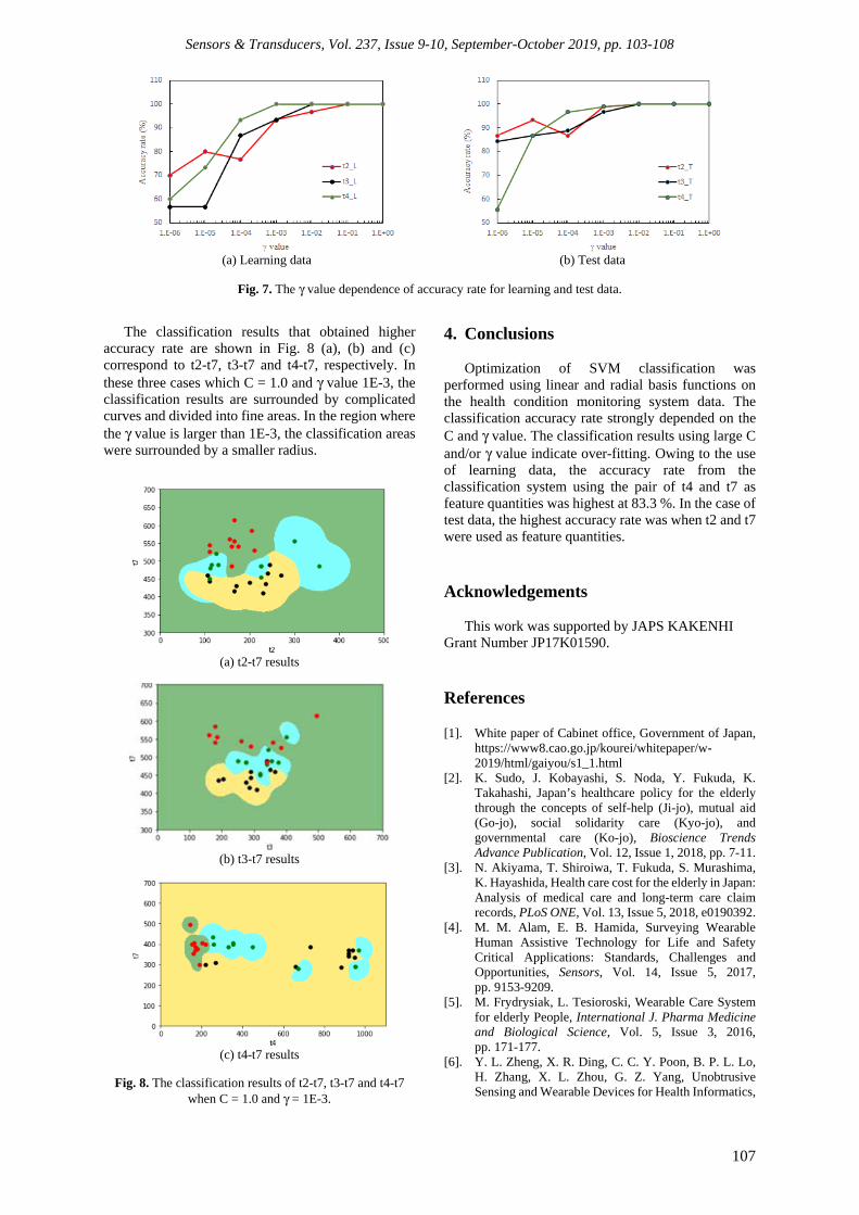
Sensors & Transducers, Vol. 237, Issue 9-10, September-October 2019, pp. 103-108
107
(a) Learning data (b) Test data
Fig. 7. The γ value dependence of accuracy rate for learning and test data.
The classification results that obtained higher accuracy rate are shown in Fig. 8 (a), (b) and (c) correspond to t2-t7, t3-t7 and t4-t7, respectively. In these three cases which C = 1.0 and γ value 1E-3, the classification results are surrounded by complicated curves and divided into fine areas. In the region where the γ value is larger than 1E-3, the classification areas were surrounded by a smaller radius.
(a) t2-t7 results
(b) t3-t7 results
(c) t4-t7 results
Fig. 8. The classification results of t2-t7, t3-t7 and t4-t7
when C = 1.0 and γ = 1E-3.
4. Conclusions
Optimization of SVM classification was performed using linear and radial basis functions on the health condition monitoring system data. The classification accuracy rate strongly depended on the C and γ value. The classification results using large C and/or γ value indicate over-fitting. Owing to the use of learning data, the accuracy rate from the classification system using the pair of t4 and t7 as feature quantities was highest at 83.3 %. In the case of test data, the highest accuracy rate was when t2 and t7 were used as feature quantities.
Acknowledgements
This work was supported by JAPS KAKENHI Grant Number JP17K01590. References [1]. White paper of Cabinet office, Government of Japan,
https://www8.cao.go.jp/kourei/whitepaper/w-2019/html/gaiyou/s1_1.html
[2]. K. Sudo, J. Kobayashi, S. Noda, Y. Fukuda, K. Takahashi, Japan’s healthcare policy for the elderly through the concepts of self-help (Ji-jo), mutual aid (Go-jo), social solidarity care (Kyo-jo), and governmental care (Ko-jo), Bioscience Trends Advance Publication, Vol. 12, Issue 1, 2018, pp. 7-11.
[3]. N. Akiyama, T. Shiroiwa, T. Fukuda, S. Murashima, K. Hayashida, Health care cost for the elderly in Japan: Analysis of medical care and long-term care claim records, PLoS ONE, Vol. 13, Issue 5, 2018, e0190392.
[4]. M. M. Alam, E. B. Hamida, Surveying Wearable Human Assistive Technology for Life and Safety Critical Applications: Standards, Challenges and Opportunities, Sensors, Vol. 14, Issue 5, 2017, pp. 9153-9209.
[5]. M. Frydrysiak, L. Tesioroski, Wearable Care System for elderly People, International J. Pharma Medicine and Biological Science, Vol. 5, Issue 3, 2016, pp. 171-177.
[6]. Y. L. Zheng, X. R. Ding, C. C. Y. Poon, B. P. L. Lo, H. Zhang, X. L. Zhou, G. Z. Yang, Unobtrusive Sensing and Wearable Devices for Health Informatics,

Sensors & Transducers, Vol. 237, Issue 9-10, September-October 2019, pp. 103-108
108
IEEE Trans. on Biomedical Engineering, Vol. 61, Issue 5, 2014, pp. 1538-1554.
[7]. M. H. Alvaro, G. Z. Begonya, M. Z. Amaia, Gait analysis Methodes: An Overview of Wearable and Non-Wearable Systems, Highlighting Clinical Applications, Sensors, Vol. 14, Issue 2, 2014, pp. 3362-3394.
[8]. S. Lee, J. Chang, Oscillometric Blood ressure Estimation Based on Deep Learning, IEEE Transactions on Industrial Informatics, Vol. 13, Issue 2, 2017, pp. 461-472.
[9]. Y. Uchida, T. Funayama, Y. Asano, Y. Kogure, Proposal for a simple care system using pressure-sensitive resistors at nursing site, in Proceedings of the International Conference of Service Science and Innovation (ICSSI’2018) and Serviceology (ICServ’2018), Taichung, Taiwan, 13-15 November 2018, p. 41.
[10]. Y. Uchida, T. Funayama, Y. Asano, Y. Kogure, Possibility for application of the machine learning to simple care system, Human Interface society SIG-ACI-22, 20, No. 11, 2018, pp. 59-62 (in Japanese).
[11]. Y. Uchida, Y. Kogure, T. Funayama, Y. Asano, A study on data classification method from healthcare monitoring system using pressure senor, Human Inferface Society SIG-ACI-23, 21, No. 2, 2019, pp. 15-18 (in Japanese).
[12]. Y. Uchida, T. Funayama, Y. Kogure, SVM classification of data obtained from a health conditon monitoring system using flexible force sensing resistors, in Proceedings of the 5th Int. Conf. on Sensors Engineering and Electronics Instrumentation Advances (SEIA’1019), Tenerife (Canary Islands), Spain, 25-27 September 2019, pp. 117-120.
__________________
Published by International Frequency Sensor Association (IFSA) Publishing, S. L., 2019 (http://www.sensorsportal.com).

Sensors & Transducers, Vol. 237, Issue 9-10, September-October 2019, pp. 109-121
109
Sensors & TransducersPublished by IFSA Publishing, S. L., 2019
http://www.sensorsportal.com
IndusBee 4.0 – Integrated Intelligent Sensory Systems for Advanced Bee Hive Instrumentation and Hive
Keepers’ Assistance Systems
1, * Andreas KÖNIG 1 Institute of Integrated Sensor Systems, TU Kaiserslautern, Erwin-Schrödinger-Str. 12,
Kaiserslautern, 67663, Germany 1 Tel.: +496312053696, fax: +496312053889
E-mail: [email protected]
Received: 30 August 2019 /Accepted: 27 September 2019 /Published: 30 November 2019 Abstract: The importance of insects, and honey bees in particular, for our ecosystem is undisputed. Currently, environmental problems from pesticides to parasites endanger the well-being or even the existence of honey bee colonies and insects in general. This imposes an increasing load on skills and activities of hive keepers. Sensors, instrumentation, and machine learning offer solutions on the one hand to effectively instrument bee hives and on the other hand to provide efficient assistance systems for hive keepers. By advanced hive instrumentation and intelligent evaluation of the acquired information hives can be monitored more easily and with less intrusion. Like in other industrial disciplines, e.g., Industry 4.0, operation can move from scheduled to event driven activity. The development in Micro-Electrical-Mechanical-Systems and Internet-of-Things field in general allows to achieve affordable integrated monitoring solutions. However, not in all tasks a dedicated instrumentation of each hive is required, and mobile assistance systems and devices to be employed in a single instance for the whole apiary will complement the instrumentation activity and the overall approach of our IndusBee 4.0 research project. Examples of this category are, e.g., honey quality assessment tool as an extension of established hygrometers or a system for improved automation of the tedious and time consuming screening for the varroa infestation of hives. This paper provides a review of activities in the field and presents the current status of contributions to both lines of research in our IndusBee 4.0 research project. With regard to hive instrumentation, in addition to standard temperature, moisture, and weight monitoring, an approach of acoustical in-hive monitoring with automated decision making and notification implemented in-hive in a SmartComb has been pursued. Further, integrated gas sensors are currently added to the SmartComb to explore the in-hive detection of infestation and illness, e.g., (American) foulbrood. Visual flight hole inspection is successively explored by a separate system in or at the hive. With regard to hive keepers’ assistance systems, an approach automating the screening for the varroa infestation of hives was tackled first. Here, a cost-effective two step procedure, a first attention step for detecting candidate regions and a final classification step of these candidate regions, is applied. It is aspired to extend the approach to continuous in-hive varroa infestation monitoring. The integration of all information from hive instrumentation and assistance systems with data fusion and data analysis activities in apiary intelligence unit is aspired in the next step. Keywords: Multi-modal bee health monitoring, Automated varroa screening, Machine vision, Machine learning, MEMS microphones, Industry 4.0, Apiary intelligence.
http://www.sensorsportal.com/HTML/DIGEST/P_3118.htm

Sensors & Transducers, Vol. 237, Issue 9-10, September-October 2019, pp. 109-121
110
1. Introduction
The systemic relevance of insects, wild bees, and honey bees in particular, is a well-known fact and found its place in public awareness. Numerous threats from pesticides to parasites, varroa destructor in the case of honey bees, threaten these essential contributors to our ecosystem. One consequence is the need for manual pollination, as already exercised in Asia, or the intentions to automate the natural pollination service by bee-like drones. A most recent patent activity to be observed was by Walmart [24]. Activities like the ‘More than Honey’ documentary of M. Imhoof et al. or the book of Tautz [5] made the role and critical situation of bees and the implications for human life lucid to the public.
Due to these increasing challenges, hive keeping gets increasingly difficult and requires more and more skills and attention from the hive keepers. Traditionally, hive tending works on a scheduled and post mortem basis with numerous opening and inspection of the hives, which is invasive, disturbing for the bees and weakening their capabilities to resist the above named increasing challenges. The development in sensor & actuator integration technology, MEMS [7], in particular, Machine Learning, and general automation, e.g., Industry 4.0, which also makes bee drones like [24] possible, allows to introduce capable yet affordable hive instrumentation solutions to closely monitor and manage an increasing number of hives and conduct less invasive event-driven tending of bees with minimized openings at the right time. “Digital” bee keeping moves from scheduled and post mortem to predictive and event-driven operation, thus reducing effort, cost, and risk. Major bee research institutions, e.g., in Germany Hohenheim, Veitshöcheim, etc. [28-30] have dealt with related issues and goals employing in numerous cases rather costly and lab-size equipment. The ongoing vivid advance in sensor, actuator, electronics, and RF integration technology [7] provides an unprecedented leverage for well performing, yet cheap and disappearing application systems that seem to make Berkeley’s Smart-Dust vision getting reality. Relevant examples are IR cameras, which become now available both miniaturized and at dramatically reduced cost, e.g., as an extension to Apple I-Phone or the FLIR Lepton One [7]. MEMS microphones are another perfect example of this development [7]. The surging development of Technical Cognition Systems, comprised of integrated sensors, electronics, RF, energy harvesting, and Machine Learning/AI, offers a leverage and an answer for many issues met in bee keeping. Two major lines of activities can be observed, i.e., Bee Hive Monitoring by sensors, embedded systems and custom software, and Hive Keeper Assistance Systems by discrete appliances for a group of hives in an apiary. Examples of this line of activity are, e.g., honey quality assessment tool as an extension of established hygrometers or a system for improved automation of the tedious and time consuming screening for the
varroa infestation level of hives. One emerging approach for semi-automated varroa screening [25] will be discussed in this paper.
First, we will focus on the Bee Hive Monitoring with special attention to both affordable and disappearing instrumentation. As in all technical disciplines, the potential market size will determine the feasible technology for the application domain. For instance in [14] bee keeping statistics for the EU are provided, naming 14 million hives in the EU. As professional hive keepers typically have about 100 to 500 hives, price sensitive yet suitable and reliable solutions are required. Market size and cost limitation clearly advocate the use of off-the-shelf components, following up technology driving application fields, e.g., automotive, communications (smart phones), and automation/ Industry 4.0.
Numerous activities can be found in the last ten to fifteen years of teams of hive keepers and engineers, complementing the activities of major bee research institutes by practical instrumentation work in the field, e.g., [4]. This vivid spin-off and maker scene mostly focused on hive weighing by scales, temperature and moisture measurement, as well as weather station, tilt, and GPS sensing, employing affordable platforms, like Arduino or Raspberry Pi, in particular the Zero, along with affordable sensors, e.g., load cells for scale assembly for hive weight, e.g., [1,3, 8-13, 15], or feeder level monitoring. With regard to commercialization numerous bee patents have been filed, e.g., [17-21]. Actuation driven ideas are added here, e.g., for sustaining small colonies or thermal varroa treatment by suitable heaters and application procedures [20, 21].
More recently, acoustical [2, 17, 19] and visual inspection of hives, e.g., for activity/flight hole monitoring [11, 12], are beginning to be added to the instrumentation palette and the resulting data is going to be processed by appropriate methods from machine vision and machine learning [22, 23]. However, in these still few and quire recent approaches, predominantly large scale and rather costly microphone devices are used and camera systems still find restrictions in use to the limited computational power of the affordable computing platforms.
Inspired by intelligent condition monitoring (ICM) and Self-X capabilities added to automation and production systems in IIoT or Industry 4.0 field, the IndusBee 4.0 research activity has been started at ISE [32] both with Bee Hive Monitoring and Hive Keeper Assistance Systems in mind. The goal is to achieve miniaturized or integrated, affordable yet reliable sensor systems adapted to the task of bee hive monitoring and hand-held devices for apiary use and process their overall data by proven to advanced machine learning methods. In the Sections 2-4 of this paper, the initial version and application of a hive integrated acoustical monitoring system with MEMS microphones and accompanying sensors for temperature, moisture, and weight monitoring will be presented.

Sensors & Transducers, Vol. 237, Issue 9-10, September-October 2019, pp. 109-121
111
Due to the threat of the honey bee by the varroa destructor parasite, hives need regular screenings or varroa counting to estimate the degree infestation by the mite and initiate appropriate treatment procedures according to the screening outcome. Though the majority of hive keepers still relies on chemical treatment, e.g. formic acid application, numerous alternatives, e.g., acoustical treatment [54, 55] by ultrasound emissions, physical treatment by a laser based on visual analysis of bees at the flight hole [53], also found in salmon farming [52], thermal treatment [21], and, last not least, numerous activities on treatment free beekeeping, e.g., in [56-59], that in the light of expected resistance of mites to chemical treatment, rely on Darwinism in breeding robust bee populations.
Even in this latter case knowledge on infestation level of a colony would still be welcome, only the taken action would be different from conventional beekeeping.
A common form of the screening process involves the visual analysis of the hive debris and to detect and count the number of mites on a slider unit, as illustrated in Fig. 1 and estimate the might infestation level by heuristic calculation from the obtained count. This task also predominantly is delivered by manual work of the hive keepers several times in the year for every hive, which adds to the anyway increasing workload due to rising issues from pesticides to parasites and illnesses. The support or even automation of this tedious procedure seems to be natural and is regarded here as an instance of discrete assistance systems development for hive keepers [45], applicable to all hives of an apiary. There is an interesting relation to the general field of insect counting, where screening procedures, and related capture or tracking methods on insects [44], are used in various forms, e.g., to reckon insect populations and give timely information for pest population surges. Predominant manual evaluation is quite tedious, time consuming, and often contradicts the need for a swift response, e.g., the just in time deployment of a chemical agent in proportion to pest occurrence.
Insect counting can base on visual count, sweep nets application or various forms of traps, e.g., pheromones, light, sticky layer, liquids, or bait deployment [35, 40, 44]. Numerous of these procedures are destructive in the sense, that counted insects are killed.
In the case of bee keeping, varroa screening or counting can also base on such a destructive approach, also denoted as flotation method, where an amount or sample of bees is extracted from the hive, effectively drowned and the varroa releasing from their bodies is counted. There is a non-destructive version of the flotation method that covers the extracted bees with powder sugar, which also makes the varroa drop from the bees for counting without losing and just irritating the bees).
In general insect counting, further, collateral damage occurs, i.e., in pest control counting applications, also harmless and useful insects are
trapped and killed, which is both bad under environmental considerations as well as making the manual or automated recognition and evaluation procedures more hard. Naturally, the field of machine vision and machine intelligence offer a plethora of similar problems to insect counting and also numerous proven methods immediately or after modification applicable for automated screening solution [33, 34, 36-39, 41, 43].
Fig. 1. Hive with debris on sliders for varroa screening. In numerous activities, that can already deal with
amazing number of different species and sizes of insects, e.g., [37], assumptions on background and density and spacing of insects to count are made [37, 41]. Often, real data confronts with strongly varying density of insects, i.e., closely packed or even stapled on top of each other, which gives rise to hard occlusion problems. Further, natural variations in phenotypes, e.g., size and patterning, changes in appearance from alive to pass away and decaying entity, orientation as well as dissected limbs etc. make automated recognition not too easy task.
With regard to potentially adding varroa screening to hive monitoring, automation of the tedious debris analysis based visual screening or counting procedure, inspired by related work in the fields of automated industrial quality control and Industry 4.0, a machine vision and learning approach is pursued in the IndusBee 4.0 research activity, which has been scarcely visited so far [50]. However, other most interesting complementing and/or alternative approaches for the same task can be found, e.g., based on visual flight hole monitoring, e.g., [53], acoustical analyses [63], similar to the activity presented in Sections 2 to 4 of this paper, or gas sensing, e.g., [51].
The overall goal of this line of activity is to achieve a simple, as possible affordable yet reliable hive keepers’ assistance system from standard components for varroa screening in bee hives under cost constraints

Sensors & Transducers, Vol. 237, Issue 9-10, September-October 2019, pp. 109-121
112
with a sufficient screening coverage for event-driven, right, and effective, treatment decisions and also for improving the house keeping by archiving the images of hive debris together with the evaluation or counting results and providing them for higher level data analysis, also fusing with other sensory information from hive instrumentation, to an Apiary AI [45].
In Section 7-9 of this paper, the first step and results of the emerging hive keepers’ assistance system for automated vision-based varroa screening will be presented. Besides technical improvement, the long term objective is the achieving and adding of hive-integrated continuously running multi-sensor varroa infestation level estimation to advanced hive instrumentation. In current work, both vision-based, acoustical [63], as well as VOC integrated gas sensor-based approaches for varroa infestation level estimation and other illness detection, similar to the remarkable recent approach in [51], which is based on discrete hive-external set-up, are under investigation.
2. SmartComb for In-Hive Monitoring
For the continued and unobtrusive measurements in a bee colony, a system based on the Raspberry Pi Zero W (OS Jessie), as in numerous other approaches, e.g., [62], has been set-up in the particular shape of an instrumented honey comb, denoted as SmartComb. The basic version incorporates two temperature and moisture sensors (DHT22/11) at top and bottom to provide readings at different hive locations. Further it includes HX711 board for hive scale reading. The key feature for this paper is the included I2S MEMS SPH0645LM4H microphone, chosen for low-cost reasons. Additionally, prototypes of high performance Infineon MEMS microphones have been made available for this work, but PDM interface requires additional electronics effort and cost, so that cheap I2S MEMS have been used in first place. Fig. 2 shows the partially assembled SmartComb prototype.
Fig. 2. SmartComb (Zander scale) prototype with acoustical, weight, temperature and moisture sensing. After completion, the depicted measurement
system was inserted in the colony center of one super and was supplied either from accu or, temporarily,
from wired 5 V supply, which limits wiring to just two wire cable from measurement unit to hive exterior. As it is well known, that bee and their by products provide a harsh environment, special care on protective packaging of sensors, cables, and embedded system have been expended, e.g., by wrapping sensors in special mesh (s. Fig. 2).
The mechanical structure of numerous MEMS sensors can be open to dirt, e.g., wax, propolis, or other hive debris. The MEMS microphone has been mounted in a way avoiding any direct path for contaminating particles, while still being sensitive to in hive sounds, and hopefully, also to vibrations on the comb it is integrated in. The SmartComb of Fig. 2 provides a hive fingerprint of two separately located temperature and moisture reading, hive weight reading, and acoustic monitoring data. Additionally, it can be of interest to have separate weight data for each super, e.g., the honey storage super, which in late summer is predominantly used for hosting the feeder module. So, also feeder module weight, proportional to filling level, can be acquired and employed for event-driven refilling. Fig. 3 shows a first prototype of a hive integrated scale for the honey storage/feeder module.
Fig. 3. Separate local scale prototype for honey storage super and feeder module weight monitoring.
The whole setup materials cost of a SmartComb is less than $ 30 for ‘lot size’ one, excluding the scale(s) setup. The following experiments have been done with such a SmartComb prototype. Adding gas sensors or cameras will of course increase possibilities and the cost. 3. Acoustical Hive State Monitoring
The acoustical monitoring of the hive state can follow the same way and principles as in predictive maintenance and Industry 4.0 based on vibration and sound monitoring, e.g., for wear-out detection and failure time prediction, e.g., [2, 6].

Sensors & Transducers, Vol. 237, Issue 9-10, September-October 2019, pp. 109-121
113
Interesting states of the bee hive are enumerated in the following, possibly not exhaustive, list:
1. Ok/Calm or Normal State; 2. Agitated/Disturbed; 3. Knocking/Pecking at hive; 4. Scratching at hive; 5. Swarm mood; 6. Missing Queen; 7. Looting …. The colony states 1-6 are mentioned also in [2, 22,
23, 63, 64] and much more relevant information, e.g., a reckoning on varroa infestation level, can potentially be taken from bee generated sounds [17, 19, 63]. Of course, dead silence in case of a perished colony hast to be taken care of in evaluation, too.
From the point of acoustical signal processing and machine learning, two general ways can be pursued after obtaining the raw data from the microphone(s) [6]. On the one hand, the classical approach based on a priori knowledge of domain-specific discriminant and invariant features followed by systematic dimension-ality reduction and classifier choice and training. This approach is both transparent and amenable to analysis and understanding (white box) and will work from small to large amount of labeled data at moderate computational cost. On the other hand, there is the currently very popular field of deep-learning neural networks, that are renowned for learning from scratch and to perform better than classical approaches, yet are not easily amenable to analysis (black box), need rich amount of labeled data, and potentially have significant computational requirements in use [6, 22, 23]. It seems worth mentioning, that there is a possible hybrid design approach pursued by ISE that merges the classical knowledge-based approach with learning or fine-tuning of system levels to rapidly achieve a transparent and well performing solution of moderate complexity [25, 26].
Thus, for the processing of the underlying sounds for reasons of transparency and hardware limitations, the classical approach was chosen with first-cut design parameters of, e.g., ROI (700 ms), 16k samples/s, and feature extraction (MFCC from python_speech_ features), optional dimensionality reduction, and classification (kNN from python sklearn with k=3) . The number of classes was selected to four with 1-4 of the previous list of possibly hive states.
The SmartComb prototype was equipped with a foundation for comb completion by bees and inserted into a bee colony, freshly established in spring 2019 (s. Fig. 4).
In addition to the possible discernment of various interesting hive states, as enumerated in the previous list, for reasons of data storage and complexity management, a hierarchical approach seems to be favorable and was pursued in the work here. It relates to a common issue known well from, e.g., Industrial Quality Control and Intelligent-Condition-Monitoring (ICM) etc.: It is fairly easy to describe the ‘Good’ or ‘Ok’ state and lots of examples are commonly available, but it is extremely hard to a priori know all
possible deviations from ‘Ok’ and acquisition of sufficient examples might be hard or even infeasible. This also relates to processing and storage requirements in data acquisition both system design as well as later on-line classification and advocates the use of one-class-classification (OCC) or anomaly or novelty detection in a hierarchical approach. These techniques are widely in use now from network intrusion problems to Industry 4.0 related ICM. The idea will be picked up in the following experimental section along with standard multi-class approach.
Fig. 4. SmartComb prepared for bee honey comb finishing (left) and inserted in a freshly established colony (right).
4. In-Hive Instrumentation Experiments and Results
The SmartComb of Fig. 4 was inserted in a living bee population and the hive was stimulated to provoke data of classes 1-4 given in the enumeration of Section 3 while continuously recording with the in-hive MEMS microphone. The obtained recordings were manually windowed, extracted, and labeled according to the meaning of the enclosed acoustical data in each window. Fig. 5 shows a feature space plot based on Sammon’s dimensionality reducing mapping of the 13-dimensional MFCC data for the four classes with 25, 20 18, and 14 samples for class 1 to 4, respectively, obtained after data preparation and labeling process.
Dimensionality reduction, e.g., by automated feature selection has been investigated by standard Sequential-Backward-Selection (SBS) with the qsi separability measure [27], but in this particular case, the potential gain for the selected best features 2, 4, 5, 9, and 10 was negligible, so the 13-dimensional data set was used in the following multi-class classification. Training the chosen kNN-classifier with all data and a k=3 setting returned a resubstitution result of ~97 % (‘OK’ always 100 %) Following, a hold-out approach was employed where, the data was

Sensors & Transducers, Vol. 237, Issue 9-10, September-October 2019, pp. 109-121
114
split up in 53 (15, 15, 12, 11) train and 28 (10, 5, 7, 6) test patterns, where 4 patterns of class 4 were present both in training and testing. Resubstitution gave ~98 % and generalization ~92.86 %.
Fig. 5. MFCC feature space plot for MEMS microphone based acoustical hive monitoring data.
For a sound statistical analysis the acquired and labeled data is still very small, but already shows the aptness of the chosen low-cost MEMS microphone, electronics, and assembly in the introduced SmartComb. In a following live test, the trained classifier was activated in the hive and the bee colony in the hive was monitored in response to status and external stimulation/excitation. The data and the classifier decisions were concurrently recorded and evaluated in the following. Fig. 6 shows an excerpt of the 475 conducted live classifications.
Fig. 6. Live classifications along with acoustical data recorded by MEMS microphone on SmartComb.
The chosen simple approach already worked well in the live test with repeated hive stimulations. Class 1 for ‘Ok’ state was always correctly discerned from all other sounds, but occasional confusion between class 2 and 4 could be observed, which was to be expected from the lower left of the feature space given in Fig. 5. The common fingerprint of the hive monitoring could now be extended by hive activity state classification as indicated in Fig. 7 for a subset of activated sensors.
The data in Fig. 7 naturally can be graphically displayed and tools and services, e.g., Thingspeak [31], are available and frequently employed.
Fig. 7. Fingerprint of hive monitoring by SmartComb (First temperature/moisture sensor and global and local scales not in use here) complemented by live acoustical activity state classification.
Sustained departure from the ‘Ok’ state can be employed to send alerts to the hive keeper and, thus, initiate event-driven maintenance. Further, the current ‘watch-dog’ classifier can also be employed to limit the potentially massive amount of recording data [22] and the following post processing effort for training and classifier refinement, by only recording raw data of not ‘Ok’ state readings. Fig. 8 tries to elucidate the idea using the data with modified labeling, assuming all not ‘Ok’ data as being novel or abnormal without trying to distinguish the cause or related class on that level. That corresponds in ICM to perceiving a deviation from the desired state of operation without bothering with the detailed classification of the type of emerging problem yet. This basically allows the training of such a simple ‘watch-dog’ or OCC classifier just by the presentation of ‘Ok’ patterns, where a rich amount of examples is commonly available. This can be achieved by various methods and implementations, e.g., by a kNN classifier with a radius limitation, which is also available in the sklearn package.
Fig. 8. Feature space plot similar to Fig. 5 with just ‘Ok’ class on a background of not ‘Ok’ or abnormal readings.
The radius limitation in kNN classification can be set manually as in rejection threshold definition or automatically computed from the available OCC training data. New sensory readings exceeding the set
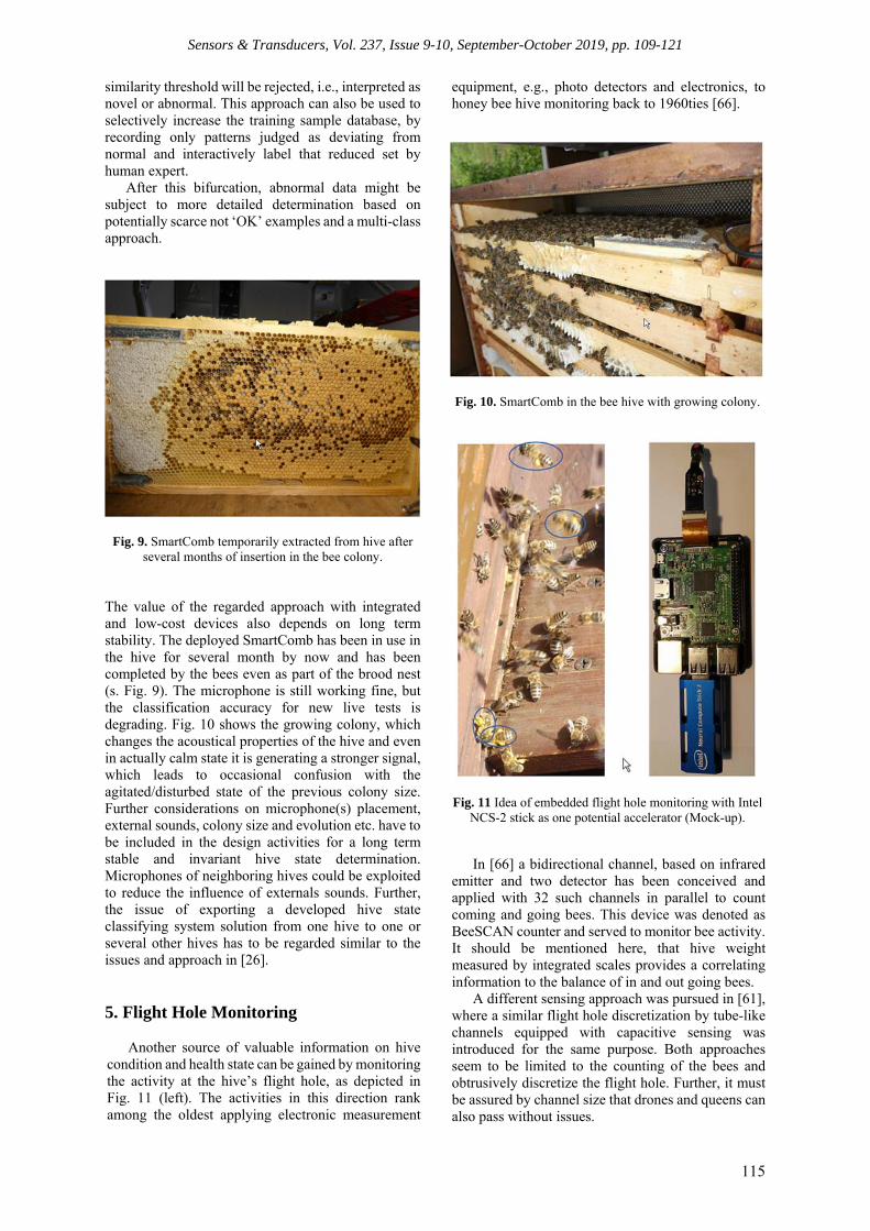
Sensors & Transducers, Vol. 237, Issue 9-10, September-October 2019, pp. 109-121
115
similarity threshold will be rejected, i.e., interpreted as novel or abnormal. This approach can also be used to selectively increase the training sample database, by recording only patterns judged as deviating from normal and interactively label that reduced set by human expert.
After this bifurcation, abnormal data might be subject to more detailed determination based on potentially scarce not ‘OK’ examples and a multi-class approach.
Fig. 9. SmartComb temporarily extracted from hive after several months of insertion in the bee colony.
The value of the regarded approach with integrated and low-cost devices also depends on long term stability. The deployed SmartComb has been in use in the hive for several month by now and has been completed by the bees even as part of the brood nest (s. Fig. 9). The microphone is still working fine, but the classification accuracy for new live tests is degrading. Fig. 10 shows the growing colony, which changes the acoustical properties of the hive and even in actually calm state it is generating a stronger signal, which leads to occasional confusion with the agitated/disturbed state of the previous colony size. Further considerations on microphone(s) placement, external sounds, colony size and evolution etc. have to be included in the design activities for a long term stable and invariant hive state determination. Microphones of neighboring hives could be exploited to reduce the influence of externals sounds. Further, the issue of exporting a developed hive state classifying system solution from one hive to one or several other hives has to be regarded similar to the issues and approach in [26]. 5. Flight Hole Monitoring
Another source of valuable information on hive condition and health state can be gained by monitoring the activity at the hive’s flight hole, as depicted in Fig. 11 (left). The activities in this direction rank among the oldest applying electronic measurement
equipment, e.g., photo detectors and electronics, to honey bee hive monitoring back to 1960ties [66].
Fig. 10. SmartComb in the bee hive with growing colony.
Fig. 11 Idea of embedded flight hole monitoring with Intel
NCS-2 stick as one potential accelerator (Mock-up).
In [66] a bidirectional channel, based on infrared emitter and two detector has been conceived and applied with 32 such channels in parallel to count coming and going bees. This device was denoted as BeeSCAN counter and served to monitor bee activity. It should be mentioned here, that hive weight measured by integrated scales provides a correlating information to the balance of in and out going bees.
A different sensing approach was pursued in [61], where a similar flight hole discretization by tube-like channels equipped with capacitive sensing was introduced for the same purpose. Both approaches seem to be limited to the counting of the bees and obtrusively discretize the flight hole. Further, it must be assured by channel size that drones and queens can also pass without issues.
Sensors & Transducers, Vol. 237, Issue 9-10, September-October 2019, pp. 109-121
116
Thus, and with the objective to obtain more information, several approaches set out to use camera systems of various complexity to unobtrusively count, but also track bees, and analyze their behavior, e.g., [10, 12, 13, 53, 60, 62, 65, 67]. More information could be gained by detecting the payload of the bees, e.g., the amount of pollen entering the hive, and potential extrapolation on breeding activity, as suggested in Fig. 11 (left). Other goals are also related to pest control and infestation level estimation by observing and counting abnormal bee behavior, deformed wings or other abnormalities, and, in particular, the identification and counting of varroa mites entering the hive clinging to bees [53]. The approach of [53] combines the approach with laser-based varroa annihilation. In [67] depth perception is added, e.g., by stereo cameras or time-of-flight sensors. In any case, the three-dimensional nature of the problem, i.e., bees coming in and entering also bottom-up and varroa mites clinging on top, bottom, and sides of the bees, will make an exact counting a challenging task, and the number of overall varroa infestation on the hive leaving bees in ratio to those present in the brood will vary strongly with the hive life cycle over the year.
Nevertheless, the number of bees going out, the daily losses, and the information of pollen intake will, together with weight information from the scale(s), give valuable information on the bee hive health condition. Further, a continuous observation could also identify the hive entering efforts of other parasites and threats from wax moths, e.g., galleria mellonella, to wasps, and the bees reaction to these as further indicators of hive fitness.
All visual flight hole monitoring activities are challenging due to large amount of data from the vision sensors, significant invariance issues, and high complexity of identification and tracking task. It might be asking too much from platforms like Raspberry Pi, but adding an efficient accelerator is one alternative to moving to more bulky and expensive computing platforms. In Fig. 11 (right), one possible option is outlined, employing an Intel Neural-Compute-Stick (NCS-2) as a recognition accelerator. This part of the IndusBee 4.0 is still in a very early phase, but the realization of an integrated low-power and low-cost vision unit for hive-integration as an additional source of information for hive health state will be pursued.
6. Emerging Integrated Gas Sensor Extension of SmartComb
Complementing the standard sensory modalities
employed for bee hive monitoring, the in-hive air can be analyzed similar to numerous applications in gas sensing, e.g., for intelligent ventilation systems in cars, smoke and fire detectors, or air quality analysis. For this purpose numerous sensors have been developed, e.g., the palette of sensors from Figaro employed in [51]. However, there are more integrated sensors
available, e.g., the air quality sensor for VOC’s SGP30-2 2.5K from Sensirion [68] that has been selected for the first extension of the SmartComb in our work. The target is to assess in-hive air quality and evaluate, whether a correlation to infestation, e.g., by varroa, or illness, e.g., (American) foulbrood can be achieved. In [51] a remarkable approach with a discrete gas sensing appliance external to the bee hives has recently been presented.
The SGP30 is a multi-pixel gas sensor for indoor air quality applications, with I2C interface and very small 2.45 × 2.45 × 0.9 mm 3 DFN package, matching well with the current SmartComb, and low-power consumption. This and related sensors from same and other manufacturers offer a very compact and robust in-hive realization. With the encouraging results of [51] in mind, this will intensively be pursued to have extended SmartComb prototypes ready for measurement in the coming bee season in 2020.
7. Visual Varroa Screening Procedure
The typical visual varroa screening process bases on the analysis of the hive debris collected on sliders as given in Fig. 12. They differ in time inserted in the hive and the amount of debris mixing with the mites to be detected. The increasing degree of debris and target varroa objects on the slider unit with insertion time leads to increasing occlusion problems up to literally burying the mites, so that attractive simple methods might fail and more computationally burdensome techniques or even sensory extensions, e.g., [43], registration techniques, e.g., fluorescence photography, and scene improvements have to be considered. As manual inspection also becomes harder, usually a time in hive of 2-3 days is recommended as feasible inspection practice, e.g., [48]. However, this will be hard to meet for the aspired continued automated screening procedure without introducing cleaning steps for the slider units.
Fig. 12. Hive debris on sliders for varroa screening illustrating possible occlusion problems aggravating with
insertion time.
A further significant challenge for an economic system version working with standard camera, e.g., available in contemporary mobile phones, is given by

Sensors & Transducers, Vol. 237, Issue 9-10, September-October 2019, pp. 109-121
117
the fact, that the inspection area of the slider is very large compared to the size of a mite. In established manual analysis, hive keepers uses multi-scale analysis by a magnifying glass and hand-eye-coordination literally excavating mites from the debris in an iterative process. Additional complexity will be added for the ambitious goal to do this automated visual varroa detection and counting repeatedly in hive, as the constrained space will make invariant data registration very hard.
One existing varroa counting system could be found in the web [50] that seems to use a similar approach as the first stage in Section 8. According to some of the comments, the approach works well for rather clean sliders and degrades with increasing cloaking and occlusion. Updates seem not be available.
8. VarroaCounter Assistance System
Our current simple first-cut VarroaCounter system concept and implementation bases on standard blob analysis, e.g. [46], which has been employed in numerous machine vision application in the last decades, is illustrated in Fig. 13.
Fig. 13. Main steps of first VarroaCounter system for a subregion of a hive slider unit.
For the first approach, it is assumed for the sake of simplicity, that the slider image is grabbed by a basic commercial still image camera, e.g., the hive keeper’s mobile phone camera, under suitable normalization conditions. Perpendicular orientation, identical scale, focus settings, as well as uniform and constant scene illumination are prerequisites for robust recognition. As in related work [34, 37], the obtained color image (see Fig. 3 top) is processed by an segmentation step, identifying possible object, or varroa occurrences, using python and scikit [46] for our simple and computationally effective mite candidate detection algorithm. Instead of computing gray value image for the segmentation step from the color registration
[34, 37], here, preliminary analysis showed the red channel itself to be best suited here for the varroa mite candidate segmentation. Under the assumption of the common white slider background and sufficient sparsity, a fixed thresholding with 15 < pij < 90 was employed returning candidate regions. A simple morphological filtering step was applied to eliminate singular region detections and smooth remaining significant regions. Then established blob analysis [46] is run, which threads all found segmentation regions and returns a blob list and number of candidate regions for further assessment (see Fig. 13 center). Enthusiastically, the resulting number could already be interpreted as the aspired varroa counting result figure. But unfortunately, this will only be true under severe and somewhat unrealistic constraints, e.g., assuming in addition to sparsity, that no other objects, e.g., insects or insect parts would be present. Thus, in the second stage of the proposed VarroaCounter, the blob regions from the list will be subject to a confirming or rejecting classification by richer features, e.g., blob properties, pixel statistics etc., computed from the initial color image registration (see Fig. 13 bottom), potentially adding structural and/or textural information to the recognition process.
9. First VarroaCounter Experiments
and Results
For the validation and improvement of the first-cut varroa counting assistance system, a collection of sliders have been accumulated from real apiary routine checks. Fig. 12 shows a few example pictures, taken by a simple still image camera. Various insertion times have led to violations of sparsity assumption and resulting occlusion problems (see Fig. 12, center). The slider samples are stored to be able to repeat recordings with different camera, scene, and illumination settings or for research application of available commercial hyper-spectral camera [49] similar to [43]. Both to check stage one of VarroaCounter and to obtain unique and ground truth data for the post classification step, shown in Fig. 14, a clean slider with only sparsely located 84 mites on it was prepared.
The stage one worked well for the easy example and returned both the correct number and list of locations of the 84 mites. For the first instance of the second, post-classification stage, a kNN classifier [47] is employed and trained with mite images given in Fig. 14 and additionally selected non-mite, background patterns. In the first place, histograms of blob regions where computed for post-classification. The corresponding, promising feature space for simple blob region histograms is shown in Fig. 15. Summarizing, the blob analysis, based on color thresholding, acceptably works with sliders sparsely populated by debris and mites.

Sensors & Transducers, Vol. 237, Issue 9-10, September-October 2019, pp. 109-121
118
Fig. 14. Clean slider for stage one test and data acquisition for second stage classifier design
Fig. 15. Feature space of the post-classifier stage.
On densely packed sliders, too large blobs arise, which are harder to rule out and require more information. Structural and color textural features [42] will be regarded next in the work to increase the counting accuracy still with affordable standard equipment.
10. Conclusions
The essential role of insects in general, and wild bees and honey bees, in particular, has reached public
awareness with increasing issues and problems, e.g., to assure pollination and related food production. An increasing number of threats from pesticides to parasites, e.g., the varroa destructor in the case of honey bees, threaten these essential contributors to our ecosystem and at the same time substantially increase the load on hive keepers to maintain and protect their bee colonies.
This situation triggered numerous activities on modifications and improvements of bee keeping. One goal of this paper was, to establish an, still evolving, survey of key activities. The main stream of engineering-based activities follow approaches in automation, including home automation, sensors, measurement, and instrumentation and set out to instrument bee hives and whole apiaries, in particular reading temperature, moisture, weight of hives as process parameters. More advanced approaches extend this to image and video analysis, e.g., for flight hole monitoring, acoustic monitoring, and in-hive air analysis by gas sensors for various purposes.
In this paper, these activities are picked up and transfer options of knowledge and methods from machine vision and learning, electronics system integration, automation, (I) IoT, ICM, and Industry 4.0 domains are exploited to provide advanced solutions, both for bee hive instrumentation and health monitoring as well as hive keeper’s assistant systems on the apiary level. An effective, disappearing, and low-cost hive-integrated approach, benefiting from the ongoing advance in micro-/nano-technologies, for the field of bee hive monitoring and colony activity and state assessment was introduced and demonstrated. A simple and low-cost approach for improving automated varroa counting [25], pursued as a building blocks in IndusBee 4.0 [45], was presented as first step for bee hive keepers assistance. The suggested two-stage procedure demonstrated by a first prototype works well under some constraints.
Fig. 16. Apiary AI proposed for aggregating and managing both hive monitoring and hive keeper assistance systems data of multi-colonies with sophisticated alerting, information, and scheduling for hive keepers.
Sensors & Transducers, Vol. 237, Issue 9-10, September-October 2019, pp. 109-121
119
In future work in our IndusBee 4.0 project [32, 25, 45] the following key issues will be pursued in the context of a hive-integrated, robust, and low-cost solution. The acoustic monitoring will be extended to a more comprehensive list of states, multi-microphone recording, advanced evaluation and adaptation strategies, and deployment to a larger number of colonies. In particular, the possibility of a correlation of bee sound information with varroa infestation level [63] will be investigated.
The SmartComb is with priority currently extended by advanced integrated gas sensors, e.g., also for potential varroa infestation level estimation and foulbrood or other illness detection [51].
The idea of visual external as well as hive-integrated continuous varroa infestation estimation will be advanced. For that aim, both presented stages have to see extension, e.g., by adding structural and color textural features [42] to overcome occlusion issues.
Visual flight hole activity monitoring will be pursued as outlined in Fig. 11., trying to collect more salient information on hive state and health condition, e.g., from pollen intake estimation or varroa infestation level estimation from varroa mites clinging to bees [53] etc. This last activity is probably the most complex one and needs further considerations for computational acceleration and appropriate choice of sensor, e.g., vision, depth, infrared, hyperspectral and related active illumination.
In particular, the creation of higher level intelligence unit, i.e., an Apiary AI as indicated in Fig. 16, that integrates data from all hives, external sources like weather stations and forecast information, and information from hive keepers’ assistance systems, will be pursued. The context available on hive and apiary level will make more efficient data analysis and hive state determination possible. Sophisticated alerting, information, and scheduling for hive keepers can thus be achieved, potentially reducing both workload and disturbing of bees. For instance, varroa infestation level estimation could be consolidated by fusing information from various sources, e.g., visual (automated) counting, sound analysis, and hive-air analysis. Swarm prediction could be improved by fusing temperature development and sound analysis in hives etc.
References [1]. Beekeeping with Arduino (https://www.hackster.io/
pvalyk/beekeeping-with- arduino-4216bb) [2]. Modular Sensor Systems for Industry 4.0,
(https://moses-pro.de/) [3]. OSBeehives (https://www.osbeehives.com/) [4]. P. Wallich, Beehackers – Cheap widgets are like
honey to hive keepers, IEEE Spectrum, May 2011, pp. 20-21.
[5]. J. Tautz, Phänomen Honigbiene, Spektrum Akademischer Verlag, 2007.
[6]. W. Zhang, G. Peng, C. Li, Y. Chen, Z. Zhang, A new deep learning model for fault diagnosis with good anti-
noise and domain adaptation ability on raw vibration signals, Sensors, Vol. 17, 2017, p. E425.
[7]. Yole Developpement, Technology Reports and Roadmaps (www.yole.fr)
[8]. Ken Meyer (https://hackaday.io/project/beemon) [9]. BeeManager (https://www.beemanager.de/) [10]. Honey Bee Counter using Arduino
(https://duino4projects.com/honey-bee-counter-using- arduino/)
[11]. IoBEE (http://users.telenet.be/iobee/index_en.html) [12]. BeeCounter (http://duino4projects.com/honey-bee-
counter-using-arduino/) [13]. BeeMonitor (https://beemonitor.org/) [14]. M.-P. Chauzat, L. Cauquil, L. Roy, S. Franco,
P. Hendrikx, M. Ribiere-Chabert, Demographics of the European Apicultural Industry, (https://www.ncbi.nlm.nih.gov/pmc/articles/PMC3827 320/pdf/pone.0079018.pdf)
[15]. HoneyPi (https://www.honey-pi.de/) [16]. V. Suta, et al, Apiary Monitoring System, Patent
Application WO 2015/048308 A1, Solutionbee LLC, 25.09.2014.
[17]. J. Bromenschenk, C. Henderson, R. Seccomb, S. Rice, R. Etter, Honey Bee Acoustic Recording and Analysis System for Monitoring Hive Health, US Patent 7549907B2, USA, 2007.
[18]. E. C. Cook, Compositions and Methods for the Treatment and Management of Bee Hives and the Bees Therein, U.S. Patent 7,922,559 B2, USA, 2011.
[19]. T. J. Brundage, Acoustic Sensor for Beehive Monitoring, US Patent 8,152,590 B2, USA, 2012.
[20]. G. Sinanis, G. Lambropoulos, Beehive Frame and Comb Foundation for Controlling Varroa Miites, US Patent 8,272,921 B2, USA, 2012.
[21]. R. Linhart, Method of a Thermal Treatment of Bee Colonies and a Device for Pursuance of This Method, US Patent 9,363,984 B2, USA, 2016.
[22]. V. Kulyukin, S. Mukherjee, P. Amlathe, Toward audio beehive monitoring: deep learning vs. standard machine learning in classifying beehive audio samples, Appl. Sci., Vol. 8, 2018, 1573.
[23]. I. Nolasco, A. Terenzi, S. Cecchi, S. Orcioni, H. L. Bear, E. Benetos, Audio-based identification of beehive states, arXiv:1811.06330v2, February 2019.
[24]. C. Gohd, Autonomous Robot Bees Are Being Patented by... Walmart? (https://futurism.com/robot- bees-drones-walmart)
[25]. A. König, VarroaCounter – Towards Automating the Varroa Screening for Alleviated Bee Hive Treatment, in Proceedings of the 5th International Conference on Sensors Engineering and Electronics Instrumentation Advances (SEIA'2019), 2019, pp. 244-247.
[26]. M. Eberhardt, S. Roth, A. König, Industrial application of machine-in-the-loop-learning for a medical robot vision system – Concept and comprehensive field study, J. Computers and Electrical Engineering (CEE), Vol. 34, March, 2008, pp. 111-126.
[27]. K. Thongpull, A. König, Advance and case studies of the DAICOX framework for automated design of multi-sensor intelligent measurement systems, Technisches Messen, Vol. 83, Issue 4, 2016, pp. 234-243.
[28]. Deutscher Imkerbund (https://deutscherimkerbund.de/ 152-Adressen_Forschungsinstitute)
[29]. IBRA (https://www.ibrabee.org.uk/) [30]. JKI (https://www.julius-kuehn.de/en/bee-protection/) [31]. IoT Analytics Thingspeak (https://thingspeak.com/)

Sensors & Transducers, Vol. 237, Issue 9-10, September-October 2019, pp. 109-121
120
[32]. IndusBee 4.0 (https://www.eit.uni- kl.de/koenig/ gemeinsame_seiten/projects/ IndusBee_40.html)
[33]. Y. Zhong, J. Gao, Q. Lei and Y. Zhou, A vision-based counting and recognition system for flying insects in intelligent agriculture, Sensors, Vol. 18, 2018, 1489.
[34]. C. Zhu, J. Wang, H. Liu, H. Mi, Insect identification and counting in stored grain: image processing approach and application embedded in smartphones, Hindawi Mobile Information Systems, Vol. 2018, 2018, 5491706.
[35]. B. Brader, R. C. Lee, R. Plarre, W. Burkholder, G. Barrie Kitto, C. Kao, L. Polston, E. Dorneanu, I. Szabo, B. Mead, B. Rouse, D. Sullins, R. Denning, A comparison of screening methods for insect contamination in wheat, Journal of Stored Products Research, Vol. 38, 2002, pp. 75-86.
[36]. Zuse Institute, Similarity Search and Insect Classification (https://www.zib.de/features/similarity- search-and-insect-classification)
[37]. K. Mele, Insect soup challenge: Segmentation, counting, and simple classification, in Proceedings of the IEEE International Conference on Computer Vision Workshops (NSW’13), Sydney, 2013, pp. 168-171.
[38]. Y. Ovadia, Y. Halpern, D. Krishnan, J. Livni, D. Newburger, R. Poplin, Ti. Zha, D. Sculley, Learning to count mosquitoes for the sterile insect technique, in Proceedings of the 23rd SIGKDD Conference on Knowledge Discovery and Data Mining (KDD’17), Halifax, NS, Canada, August 13-17, 2017.
[39]. G. Sileshi, A method for estimating insect abundance and patch occupancy with potential applications in large-scale monitoring programmes, African Entomology, Vol. 15, Issue 1, 2007, pp. 89-101.
[40]. G. Zehnder, Overview of monitoring and identification techniques for insect pests, Organic Agriculture, March 12, 2014, 20140312.
[41]. SpecialVideo, Insects Counting for Integrated Pest Control (https://www.specialvideo.it/en)
[42]. C. Palm, Color texture classification by integrative Co-occurrence matrices, Pattern Recognition, Vol. 37, Issue 5, May 2004, pp. 965-976.
[43]. J. Fennel, C. Veys, J. Dingle, J. Nwezeobi, S. van Brunschot, J. Colvin, B. Grieve, A method for realtime classification of insect vectors of mosaic and brown streak disease in cassava plants for future implementation within a lowcost, handheld, in field multispectral imaging sensor, Plant Methods, Vol. 14, 2018, 82.
[44]. CDFA, Insect Trapping Guide (https://www.cdfa. ca.gov/plant/PDEP/Insect_Trapping_Guide/docs/Insect_Trapping_Guide_web.pdf)
[45]. A. König, Extending bee hive health state monitoring by integrated acoustical sensing and machine learning, in Proceedings of the 5th International Conference on Sensors Engineering and Electronics Instrumentation Advances (SEIA'2019), Tenerife (Canary Islands), 25-27 September 2019, pp. 168-173.
[46]. Blob Detection (https://scikit-image.org) [47]. kNN-Classification (https://scikit-learn.org) [48]. Bayerische Landesanstalt für Weinbau und Gartenbau,
Gemülldiagnose (https://www.lwg.bayern.de/mam/ cms06/bienen/dateien/gem%C3%BClldiagnose_fzbienen2012.pdf)
[49]. Photon Focus (http://www.photonfocus.com/de/) [50]. Varroazählen leicht gemacht (Software)
(http://www.imker-kiel.de/news/molfsee-mit-horst/67varroacount.html)
[51]. A. Szczurek, M. Maciejewska, B. Bąk, J. Wilk, J. Wilde, M. Siuda, Detection Level of Honeybee Desease: Varroosis Using a Gas Sensor Array, in Proceedings of the 5th International Conference on Sensors Engineering and Electronics Instrumentation Advances (SEIA'2019), Tenerife (Canary Islands), 25-27 September 2019, pp. 255-256.
[52]. M. Dumiak, Lice-Hunting Underwater Drone Pro-tects Salmon, IEEE Spectrum, April 2017, pp. 9-10.
[53]. L. Chazette, M. Becker and H. Szczerbicka, Basic algorithms for bee hive monitoring and laser-based mite control, 2016 IEEE Symposium Series on Computational Intelligence (SSCI), Athens, 2016, pp. 1-8.
[54]. R. Krüger, Varroa Sound (https://www.varroa-killer sound.com/)
[55]. Wirkt der Varroa-Killer-Sound® doch?, Bienen & Natur, 27 Januar 2018 (https://www.bienenundnatur.de/fachthemen/leserbriefe-diskussion/wirkt-der-varroa-killer-sound-doch/)
[56]. C. Hudson and S. Hudson, Varroa has lost its sting, The British Bee Journal, December 2016 (https://beemonitor.files.wordpress.com/ 2016/07/429_varroa.pdf)
[57]. F. Gellatly, Varroa: to treat or not to treat? The Welsh Beekeeper, 191, Winter 2015.
[58]. C. Hudson and S. Hudson, Notes on Treatment Free Beekeeping, January 2018 (https://beemonitor.files. wordpress.com/2018/04/notes-on-treatment-free-beekeeping-jan-2018.pdf)
[59]. C. Blauert, Treatment-free beekeeping and feral bees, Visit Report, May 2018, https://www.mellifera.de/download.html?f=downloads%2FTreatment-free+beekeeping+and+feral+bees+-+a+visit+to+Clive+and+Shan+Hudson%2C+Snowdonia%2C+2nd+May+2018.pdf
[60]. J. Salas and P. Vera, Counting the Bumblebees Entering and Leaving a Beehive, in Proceedings of the 21st International Conference on Pattern Recognition (ICPR 2012), 2012.
[61]. J. M. Campbell, D. C. Dahn and D. A. J .Ryan, Capacitance-based sensor for monitoring bees passing through a tunnel, Measurement Science and Technology, Volume 16, Number 12, Nov. 2005, p. 2503.
[62]. R. Tashakkori, N. P. Hernandez, A. Ghadiri, A. P. Ratzloff and M. B. Crawford, A honeybee hive monitoring system: From surveillance cameras to Raspberry Pis, in Proceedings of the IEEE SoutheastCon 2017 Conference, Charlotte, NC, 2017, pp. 1-7.
[63]. A. Qandour, I. Ahmad, D. Habibi, and M. Leppard, Remote beehive monitoring using acoustic signals, Acoustics Australia, 42, 3, 2014, pp. 204-209.
[64]. D. Howard, O. Duran and G. Hunter, A Low-Cost Multi-Modal Sensor Network for the Monitoring of Honeybee Colonies/Hives, in Ambient Intelligence and Smart Environments, Volume 23: Intelligent Environments 2018, IOS Press, 2018, pp. 69 – 78.
[65]. J. A. Campbell, L. B. Mummert, and R. Sukthankar, Video Monitoring of Honey Bee Colonies at the Hive Entrance, in Proceedings of the Workshop Vis Observation Anal Anim Insect Behav (ICPR), 2008.
[66]. M. Struye, H. Mortier, G. Arnold, C. Miniggio, and R. Borneck, Microprocessor-controlled monitoring of honeybee flight activity at the hive entrance, Apidologie, Vol. 25, No. 4, 1994, pp. 384–395.
[67]. G. Chiron, P. Gomez-Krämer, and M. Ménard, Detecting and tracking honeybees in 3D at the beehive

Sensors & Transducers, Vol. 237, Issue 9-10, September-October 2019, pp. 109-121
121
entrance using stereo vision, EURASIP Journal on Image and Video Processing, 59, 2013, 2013, pp. 1-17.
[68]. Sensirion, Datasheet SGP30 Sensirion Gas Platform (www.sensirion.com)
__________________
Published by International Frequency Sensor Association (IFSA) Publishing, S. L., 2019 (http://www.sensorsportal.com).
Sensors & Transducers, Vol. 237, Issue 9-10, September-October 2019, pp. 122-128
122
Sensors & Transducers
Published by IFSA Publishing, S. L., 2019 http://www.sensorsportal.com
Negative Ion Instrumentation for Detection of the Electron Affinity of Astatine
Lars E. Bengtsson
University of Gothenburg, Kemivägen 9, 412 96 Gothenburg, Sweden Tel.: +4631 786 9128
E-mail: [email protected]
Received: 30 August 2019 /Accepted: 27 September 2019 /Published: 30 November 2019 Abstract: For the purpose of measuring the electron affinity of Astatine, a versatile tool for ion beam line up is proposed. Apertures in the ion optics are used to guide the beam and traditionally the current is measured on the apertures in order to detect the presence of an ion beam. By slitting the aperture into four separate pieces, the aperture current can also be used to determine the direction of the misalignment and the size of the ion beam diameter. A 4-channel pico ammeter with optical LED indication of the ion beam position is suggested in an analog/digital hybrid design. The design utilizes two charge/current-to-digital chips in a microcontroller design. This work is an important contribution to an ongoing project with the objective to determine the electron affinity of Astatine which is a potential α-radiation agent in radioimmunotherapy. Keywords: Ion optics, Astatine, Pico ammeter, α-radiation, Radioimmunotherapy, Microcontroller. 1. Introduction
1.1. Background
Radiation therapy is one of the most common treatments for cancer; cancer cells are destroyed by ionizing radiation. However, ionizing radiation may also cause damage to healthy cells and in any radiation therapy it is paramount that the radiation is focused on the cancer cells and avoid non-cancerous cells as much as possible. For example, different radiation angles can be applied in order to minimize the radiation exposure of healthy cells.
Ionizing radiation comes in three different shapes; α-radiation, β-radiation and γ-radiation. α-radiation is basically helium nuclei and the advantage of using α-radiation in cancer therapy is that they cause a lot of damage to the cancer cells due their large impact force; once they penetrate the cell membrane, they shatter the DNA molecule. The disadvantage is that they have a very short range; due to their large size, they interact
with surrounding particles and will only travel a few centimeters in air. In order to be used in cancer therapy, they must be injected into the body (brachy therapy) and they are likely to cause as much damage to health tissue as they do to cancer cells.
β-radiation consists of electrons. They are smaller than α-particles and therefore they have a longer range; they can penetrate human skin down to approximately 1 cm. Hence, if tumors are deeper than 1 cm, the β-radiator must also be injected into the body (with similar consequences as α-particles). Also, since electrons are lighter than helium nuclei, a higher radiation dose is required compared to α-radiation.
γ-radiation is high-energetic electromagnetic radiation which easily penetrates the human body and destroys cancer cells. However, their extended range is also likely to cause a lot of “collateral” damage to healthy cells and might actually turn healthy cells into cancer cells.
http://www.sensorsportal.com/HTML/DIGEST/P_3119.htm
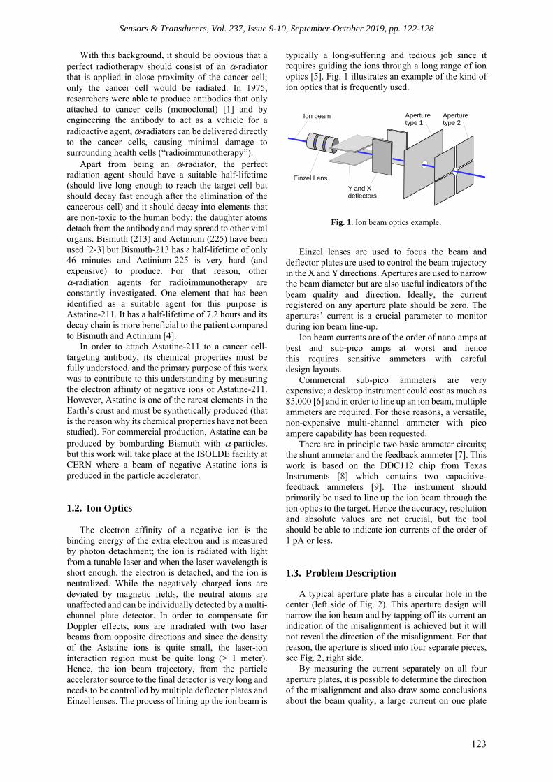
Sensors & Transducers, Vol. 237, Issue 9-10, September-October 2019, pp. 122-128
123
With this background, it should be obvious that a perfect radiotherapy should consist of an α-radiator that is applied in close proximity of the cancer cell; only the cancer cell would be radiated. In 1975, researchers were able to produce antibodies that only attached to cancer cells (monoclonal) [1] and by engineering the antibody to act as a vehicle for a radioactive agent, α-radiators can be delivered directly to the cancer cells, causing minimal damage to surrounding health cells (“radioimmunotherapy”).
Apart from being an α-radiator, the perfect radiation agent should have a suitable half-lifetime (should live long enough to reach the target cell but should decay fast enough after the elimination of the cancerous cell) and it should decay into elements that are non-toxic to the human body; the daughter atoms detach from the antibody and may spread to other vital organs. Bismuth (213) and Actinium (225) have been used [2-3] but Bismuth-213 has a half-lifetime of only 46 minutes and Actinium-225 is very hard (and expensive) to produce. For that reason, other α-radiation agents for radioimmunotherapy are constantly investigated. One element that has been identified as a suitable agent for this purpose is Astatine-211. It has a half-lifetime of 7.2 hours and its decay chain is more beneficial to the patient compared to Bismuth and Actinium [4].
In order to attach Astatine-211 to a cancer cell-targeting antibody, its chemical properties must be fully understood, and the primary purpose of this work was to contribute to this understanding by measuring the electron affinity of negative ions of Astatine-211. However, Astatine is one of the rarest elements in the Earth’s crust and must be synthetically produced (that is the reason why its chemical properties have not been studied). For commercial production, Astatine can be produced by bombarding Bismuth with α-particles, but this work will take place at the ISOLDE facility at CERN where a beam of negative Astatine ions is produced in the particle accelerator.
1.2. Ion Optics
The electron affinity of a negative ion is the
binding energy of the extra electron and is measured by photon detachment; the ion is radiated with light from a tunable laser and when the laser wavelength is short enough, the electron is detached, and the ion is neutralized. While the negatively charged ions are deviated by magnetic fields, the neutral atoms are unaffected and can be individually detected by a multi-channel plate detector. In order to compensate for Doppler effects, ions are irradiated with two laser beams from opposite directions and since the density of the Astatine ions is quite small, the laser-ion interaction region must be quite long (> 1 meter). Hence, the ion beam trajectory, from the particle accelerator source to the final detector is very long and needs to be controlled by multiple deflector plates and Einzel lenses. The process of lining up the ion beam is
typically a long-suffering and tedious job since it requires guiding the ions through a long range of ion optics [5]. Fig. 1 illustrates an example of the kind of ion optics that is frequently used.
Fig. 1. Ion beam optics example.
Einzel lenses are used to focus the beam and deflector plates are used to control the beam trajectory in the X and Y directions. Apertures are used to narrow the beam diameter but are also useful indicators of the beam quality and direction. Ideally, the current registered on any aperture plate should be zero. The apertures’ current is a crucial parameter to monitor during ion beam line-up.
Ion beam currents are of the order of nano amps at best and sub-pico amps at worst and hence this requires sensitive ammeters with careful design layouts.
Commercial sub-pico ammeters are very expensive; a desktop instrument could cost as much as $5,000 [6] and in order to line up an ion beam, multiple ammeters are required. For these reasons, a versatile, non-expensive multi-channel ammeter with pico ampere capability has been requested.
There are in principle two basic ammeter circuits; the shunt ammeter and the feedback ammeter [7]. This work is based on the DDC112 chip from Texas Instruments [8] which contains two capacitive-feedback ammeters [9]. The instrument should primarily be used to line up the ion beam through the ion optics to the target. Hence the accuracy, resolution and absolute values are not crucial, but the tool should be able to indicate ion currents of the order of 1 pA or less.
1.3. Problem Description A typical aperture plate has a circular hole in the
center (left side of Fig. 2). This aperture design will narrow the ion beam and by tapping off its current an indication of the misalignment is achieved but it will not reveal the direction of the misalignment. For that reason, the aperture is sliced into four separate pieces, see Fig. 2, right side.
By measuring the current separately on all four aperture plates, it is possible to determine the direction of the misalignment and also draw some conclusions about the beam quality; a large current on one plate
Einzel LensY and X deflectors
Aperturetype 1
Aperturetype 2
Ion beam
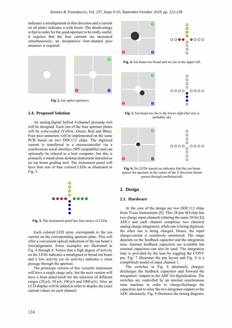
Sensors & Transducers, Vol. 237, Issue 9-10, September-October 2019, pp. 122-128
124
indicates a misalignment in that direction and a current on all plates indicates a wide beam. The disadvantage is that in order for the quad-aperture to be really useful, it requires that the four currents are measured simultaneously; an inexpensive four-channel pico ammeter is required.
Fig. 2. Ion optics apertures.
1.4. Proposed Solution An analog/digital hybrid 4-channel picoamp tool
will be designed. Each one of the four aperture plates will be color-coded (Yellow, Green, Red and Blue). Four pico ammeters will be implemented on the same PCB based on two DDC112 chips. The digitized current is transferred to a microcontroller via a synchronous serial interface (SPI compatible) and can optionally be relayed to a host computer, but this is primarily a stand-alone desktop instrument intended as an ion beam guiding tool. The instrument panel will have four sets of four colored LEDs as illustrated in Fig. 3.
Fig. 3. The instrument panel has four arrays of LEDs.
Each colored LED array corresponds to the ion current on the corresponding aperture plate. This will offer a convenient optical indication of the ion beam’s (mis)alignment. Some examples are illustrated in Fig. 4 through 6. Notice that a high degree of activity on the LEDs indicates a misaligned or broad ion beam and a low activity (or no activity) indicates a clean passage through the aperture.
The prototype version of this versatile instrument will have a single range only, but the next version will have a front panel knob for the selection of different ranges (20 pA, 50 pA, 100 pA and 1000 pA). Also, an LCD display will be added in order to display the exact current values on each channel.
Fig. 4. Ion beam too broad and too far to the upper left.
Fig. 5. Ion beam too far to the lower right (but size is probably ok).
Fig. 6. No LEDs turned on indicates that the ion beam passes the aperture in the center of the Z direction (beam
passes through unobstructed).
2. Design
2.1. Hardware At the core of the design are two DDC112 chips
from Texas Instruments [8]. This 28-pin SO-chip has two charge input channels (sharing the same 20-bit ΣΔ ADC) and each channel comprises two classical analog charge integrators; while one is being digitized, the other one is being charged. Hence, the input charge/current is seamlessly monitored. The range depends on the feedback capacitor and the integration time. Internal feedback capacitors are available but external capacitors can also be used. The integration time is provided by the user by toggling the CONV pin. Fig. 7 illustrates the pin layout and Fig. 8 is a (simplified) model of input channel 1.
The switches in Fig. 8 alternately charges/ discharges the feedback capacitors and forward the integrators’ outputs to the ADC for digitalization. The switches are controlled by an internal synchronous state machine in order to charge/discharge the capacitors and to relay the two integrator outputs to the ADC alternately. Fig. 9 illustrates the timing diagram;
Y G
R B
Y G
R B
Y G
R B
Y G
R B

Sensors & Transducers, Vol. 237, Issue 9-10, September-October 2019, pp. 122-128
125
input integrators A (on both channels) are integrated simultaneously while integrators B are being digitized by the AD converter. The signal indicates when both channels have been digitized and data is stored in a 40-bit shift register.
Fig. 7. Current-to-digital converter (DDC112).
Fig. 8. Charge-input integrator.
The user retrieves data through the synchronous serial interface (pins DCLK and DOUT). This is illustrated in Fig. 10 [10].
Transmission is initiated by the user setting the signal low and data is shifted out on the DOUT pin synchronous to the rising edges on the DCLK pin. Notice in Fig. 10 that the signal is automatically reset when transmission is initiated.
The primary concern in this design is to detect negative ion currents or electrons. However, sometimes positive ion experiments are conducted and for that reason the instrument needs to be able to detect both positive and negative currents. The DDC112 chip can easily be converted to a bipolar ammeter by adding an offset current to the input, see Fig. 11 [11].
Fig. 9. Integration timing diagram.
Fig. 10. Timing diagram of data retrieval.
Fig. 11. Bipolar input.
The ADC in the DDC112 chip has a resolution of 20 bits; if the input current equals the full-scale current (IFS), the ADC output will be 0xFFFFF (220 -1). V and R in Fig. 11 will produce an offset current V/R and this current is added to the sensor current. In order to make the instrument bipolar, V and R are dimensioned so that V/R = IFS/2.
The two currents from the sensor and the offset branch are added in the junction and the sum of the two currents are fed to the DDC112 chip. The consequence of that is that when the sensor input current ISENS = − IFS/2, the input current to the DDC112 chip is zero. Table 1 illustrates the consequence of the offset current. From Table 1 it is obvious that the instrument is now bipolar.
28IN2
27AGND
26CAP2B
25CAP2B
24CAP2A
23CAP2A
22VREF
21AGND
20RANGE2
19RANGE1
18RANGE0
17DVALID
16DOUT
15DGND
1
2
3
4
5
6
7
8
9
10
11
12
13
14
IN1
AGND
CAP1B
CAP1B
CAP1A
CAP1A
AVDD
TEST
CONV
CLK
DCLK
DXMIT
DIN
DVDD
DD
C11
2
−+
Iin
CF1AVref
Int1A
20-bit ΣΔ ADC
−+
CF1BVref
Int1BTo Channel 2
ADCCONV
Int1B Int2B Int1A Int2A
Int2B Integrate
Int2A Integrate
Int1B Integrate
Int1A Integrate
CONV
DVALID
MSB LSB MSB LSBDOUT
In2: 20 bits In1: 20 bits
DCLK
DXMIT
DVALID
From sensor
1 IN1
DD
C11
2
V
R
IFS/2
ISENS
ISENS + IFS/2
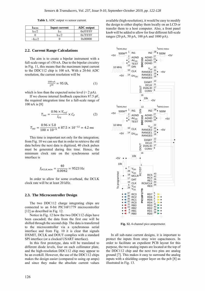
Sensors & Transducers, Vol. 237, Issue 9-10, September-October 2019, pp. 122-128
126
Table 1. ADC output vs sensor current.
ISENS Input current ADC output
IFS/2 IFS 0xFFFFF 0 IFS/2 0x7FFFF
−IFS/2 0 0x00000
2.2. Current Range Calculations The aim is to create a bipolar instrument with a
full-scale range of ±50 nA. Due to the bipolar circuitry in Fig. 11, this means that the maximum input current to the DDC112 chip is 100 nA. With a 20-bit ADC resolution, the current resolution will be
nA = 95fA, (1)
which is less than the expected noise level (≈ 2 pA). If we choose internal feedback capacitors 87.5 pF,
the required integration time for a full-scale range of 100 nA is [8]
= 0.96 × × (2)
= 0.96 × 5.0100 × 10 × 87.5 × 10 = 4.2 ms
This time is important not only for the integration; from Fig. 10 we can see that in order to retrieve the old data before the next data is digitized, 40 clock pulses must be generated during this time. Hence, the minimum clock rate on the synchronous serial interface is
, = 400.0042 = 9523Hz
In order to allow for some overhead, the DCLK
clock rate will be at least 20 kHz.
2.3. The Microcontroller Design The two DDC112 charge integrating chips are
connected to an 8-bit PIC16F1779 microcontroller [12] as described in Fig. 12.
Notice in Fig. 12 how the two DDC112 chips have been cascaded; the data from the first one will be shifted through the second chip. The data is transferred to the microcontroller via a synchronous serial interface and from Fig. 10 it is clear that signals DXMIT, DCLK and DOUT complies with a standard SPI interface (or a clocked USART interface).
In this first prototype, data will be translated to different diode levels, four on each collimator plate, and the high-resolution DDC112 chip may appear to be an overkill. However, the use of the DDC112 chips makes the design easier (compared to using op amps) and since they make the absolute current values
available (high-resolution), it would be easy to modify the design to either display them locally on an LCD or transfer them to a host computer. Also, a front panel knob will be added to allow for four different full-scale ranges (20 pA, 50 pA, 100 pA and 1000 pA).
Fig. 12. 4-channel pico ampermeter.
In all sub-nano current designs, it is important to protect the inputs from stray wire capacitances. In order to facilitate an expedient PCB layout for this purpose, the two analog inputs are located at the top of the DDC112 chip and the next two pins are analog ground [7]. This makes it easy to surround the analog inputs with a shielding copper layer on the pcb [8] as illustrated in Fig. 13.
1 IN1
DD
C11
2
ISENS,Blue
+5VAGNDAVDDTESTDIN
500M278
13
CLK10 MHz
DVDD+5V
28IN2
ISENS,Yellow
+5V500M
27
22
AGNDAGNDDGND
2115
VrefRANGE2RANGE1RANGE0
+5V201918
DO
UT
DXMITDCLK
DVALIDCONV
1211179
16
1 IN1
DD
C11
2
ISENS,Red
+5VAGNDAVDDTEST
500M278
13
CLK10 MHz
DVDD+5V
28IN2
ISENS,Green
+5V
500M27
22
AGNDAGNDDGND
2115
VrefRANGE2RANGE1RANGE0
+5V201918
DO
UT
DXMITDCLK
DVALIDCONV
1211179
16
DIN
+5V10k
1
+5V
RC
7/D
TVDDVDDMCLRDATCLKVSSVSS
RC3RC2RC1RC0RB3RB2RB1RB0
RD7RD6RD5RD4RD3RD2RD1RD0
10
14
10
14
629
37363532111098
543241403938
161718
10k
287
10k
To p
rogr
amm
er
RC5RC4RE1
RC6/CLKRE0 25
44264243
PIC
16F
177
9

Sensors & Transducers, Vol. 237, Issue 9-10, September-October 2019, pp. 122-128
127
Fig. 13. Input signals are protected from stray capacitances.
3. Related/previous Work
The DDC112 chip is a common solution to low-current/low-charge problems. It has been used in precise current integrators in scanning tunneling microscopes and atomic force microscopy [13], measuring sub-picoamp currents from Faraday cup detectors [14], ion beam monitoring in deep proton lithography [15] and as photometric analyzers in optical telescopes [16]. The idea explored in this work, where an ion optics collimator plate is split into four symmetric pieces, was first suggested by Snowden and Barber [17] but their application was for microamp currents and used shunting resistors in a bridge to detect the current. The main difference of this work is that it utilizes the versatile DDC112 chip (based on charged integration), it has the option to transfer absolute current values to a host computer and offers the convenient visual indication of the beam position facilitated by the front panel LEDs.
Astatine is a halogen element, located right below Iodine in the periodic table, and its chemical properties are expected to be close to that of Iodine. The electron affinity of iodine has previously been measured to 3.059 038(10) eV [18]. Since the Astatine has one more electron orbit than Iodine, the extra electron in the negative Astatine ion will be further away from the nucleus and the electrostatic attraction force will be smaller; the electron affinity of Astatine is expected to be less than that of Iodine. This is also in accordance with theoretical predictions which range from 2.30 to 2.90 eV [19-21].
Different tumors have different antigens and therefore the antibody-antigen biding differs for different kinds of tumors; the antibody must be designed specifically for the active tumor’s antigens and the chemical bonding between the radiation agent and the antibody must be strong enough, so that it isn’t released before it has reached the cancer cell; once the antibody has docked with the antigens, the antibody is absorbed by the cell and the radiation agent can destroy the DNA protein in the cell nucleus. The antibody with the radiation agent is illustrated in Fig. 14, and Fig. 15 illustrates the antibody-antigen bonding. Fig. 16 illustrates how the cell nucleus (holding the DNA molecule) is exposed to α-radiation once the antibody has penetrated the cell surface.
This method was first practiced in 1958 when it was used in leukemia therapy [22]. However, in “solid” tumors, the penetration rate is poor and for that
reason non-internalizing antibody-drugs are being researched [23-24].
Fig. 14. Antibody as a vehicle for anti-cancer drug.
Fig. 15. Antibodies are designed to attach only to carcinogenic cells (of a specific kind).
Fig. 16. Antibodies are designed to attach only to carcinogenic cells (of a specific kind).
4. Conclusions A microcontroller based, 4-channel pico ammeter
is being developed for the purpose of facilitating convenient line up of ion beams in particle physics experiments at the GANDALPH setup at the CERN-ISOLDE facility. Instead of devolving to discrete feedback opamp solutions, two, 2-channel charge integrating chips are employed. This solution is less expensive, more robust, simplifies PCB layout and facilitates a digital interface for retrieving the absolute current value.
A prototype will be tested in October 2019 and beta testing will be performed in the Atomic Physics Laboratories in Gothenburg during the fall before the instrument is shipped to the CERN ISOLDE facility later this year.
28IN2
27AGND
26CAP2B
1
2
3
IN1
AGND
CAP1B
DD
C11
2
Antibody
α-radiation agent
Chemical bond
Cancer cell
Antigens
Cancer cell

Sensors & Transducers, Vol. 237, Issue 9-10, September-October 2019, pp. 122-128
128
Acknowledgements
The preliminary version of this work was first presented at the 5th International Conference on Sensors and Electronic Instrumentation Advances 2019 [25]. The author has no other conflicts of interest to report. References [1]. G. Kohler, C. Milstein, Continuous cultures of fused
secreting antibody of predefined destiny, Nature, Vol. 256, 1975, pp. 495-497.
[2]. M. McDevitt, G. Sgouros, R. D. Finn, J. L. Humm, J. Juric, S. Larson, D. Scheinberg, Radioimmunotherapy with alpha-emitting nuclides, European Journal of Nuclear Medicine, Vol. 25, Issue 9, 1998, pp. 1341-1351.
[3]. J. Juric, Clinical Studies with Bismuth-213 and Actinium-225 for Hematologic Malignancies, Current Radiopharmaceuticals, Vol. 11, Issue 3, 2018, pp. 192-199.
[4]. M. Zalutsky, M. Pruszynski, Astatine-211: Production and Availability, Current Radiopharmaceuticals, Vol. 4, Issue 3, 2011, pp. 177-185.
[5]. D. A. Skoog, J. J. Leary, Principle of Instrumental Analysis, 4th ed., Saunders College Publishing, Orlando, Florida, 1992, pp. 429-432.
[6]. Tektronix Inc., Keithley Series 6400 Picoammeters, Tektronix, Inc., 19 March 2018. [Online]. Available: https://www.tek.com/keithley-low-level-sensitive-and-specialty-instruments/keithley-series-6400-picoammeters. [Accessed 19 March 2018].
[7]. Keithley Instruments, Inc., Low Level Measurments Handbook, 6th ed., Keithley Instruments, Inc., Cleveland, Ohio, 2004.
[8]. Texas Instruments, Burr-Brown, DDC112: Dual Current Input 20-bit Analog-to-Digital Converter, Texas Instruments, 2004.
[9]. A. A. Mortuza, F. Pervez, K. Hossain, S. K. Sen, N. H. Mia, M. K. Basher, S. Alam, Pico-current Measurement Challenges and Remedies: A Review, Universal Journal of Engineering Science, Vol. 5, Issue 4, 2017, pp. 57-63.
[10]. J. Todsen, Retrieving data from the DDC112, Burr-Brown Corporation, Tucson, Arizona, 1998.
[11]. J. Todsen, Creating a bipolar input range for the DDC112, Burr-Brown Corporation, Tucson, Arizona, 1999.
[12]. PIC16(L)F1777/8/9, Microchip Technology Inc., Tucson, Arizona, 2015-2016.
[13]. K. Raczkowski, T. Piasecki, M. Rudek, T. Gotszalk, Design and evaluation of precise current integrator for scanning probe microscopy, Measurement Science and Technology, Vol. 28, Issue 3, 2017, pp. 1-9.
[14]. S. Agosteo, E. Borsato, F. Corso, A. Fazzi, F. Gonella, M. Intrioni, I. Lippi, M. Lorenzoli, L. Modense, F. Montecassiano, M. Pegoraro, A. Pola, V. Varoli,
P. Zotto, Performance of a proton irradiation chamber, Nuclear Instruments and Methods in Physics Research Section A: Accelerator, Spectrometers, Detectors and Associated Equipment, Vol. 664, Issue 1, 2012, pp. 193-202.
[15]. P. Vynck, B. Volckaerts, M. Vervaeke, H. Ottevare, P. Tuteleers, L. Cosentino, P. Fincchiaro, A. Pappalardo, A. Hermanne, H. Thienpont, Beam monitoring enhances deep proton lithography: towards high-quality micro-optical components, in Proceedings of the Symposium IEEE/LEOS Benelux Chapter, Amsterdam, 2002.
[16]. R. S. Romaniuk, Space and High Energy Experiments Advanced Electronic Systems 2012, Intternational Journal of Electronics and Telecommunications, Vol. 58, Issue 4, 2012, pp. 441-462.
[17]. K. Snowdon, C. Barber, Simple accelerator beam position monitor, Journal Physics E: Scientific Instruments, Vol. 12, Issue 10, 1979, p. 923.
[18]. D. Hanstorp, M. Gustafsson, Determination of the electron affinity of iodine, Journal of Physics B: Atomic, Molecular and Optical Physics, Vol. 25, Issue 8, 1992, pp. 1773-1783.
[19]. A. Mitin, C. van Wullen, Two-component relativistic density-functional calculations of the dimers of the halogens from bromine through element 117 using effective core potential and all-electron methods, Journal of Chemical Physics, Vol. 124, 2006, 064305.
[20]. H. Hotop, W. Lineberger, Binding Energies in Atomic Negative Ions: II, Journal of Physical and Chemical Reference Data, Vol. 14, Issue 3, 1985, pp. 731-750.
[21]. S. Hughes, U. Kaldor, The Fock-space coupled-cluster method: Electron affinities of the five halogen elements with consideration of triple excitations, Journal of Chemical Physics, Vol. 99, Issue 9, 1993, pp. 6773-6776.
[22]. G. Mathé, T. Loc and J. Bernard, Effet sur la leucemie 1210 de la souris d’un combinaison par diazotation d’A-methopterin et de γ-globulines de hamsters porteurs de cette leucemie par heterograffe, Comptes Rendus de l'Académie des Sciences, Vol. 216, 1958, pp. 1626-1628.
[23]. Joubert N., Denevault-Sabourin C., Bryden F., Viaud-Massuard M.-C., Towards antibody-drug conjugates and prodrug strategies with extracellular stimuli-responsive drug delivery in the tumor microenvironment for cancer therapy, European Journal of Medicinal Chemistry, Vol. 142, 2017, pp. 393-415.
[24]. A. D. Corso, R. Gébleux, P. Murer, A. Soltermann, D. Neri, A non-internalizing antibody-drug conjugate based on an anthracycline payload displays potent therapeutic activity in vivo, Journal of Controlled Release, Vol. 264, 2017, pp. 211-218.
[25]. L. Bengtsson, An Ion Beam Guidance Control Tool Proposal, in Proceedings of the 5th International Conference on Sensors and Electronic Instrumentation Advances (SEIA’ 2019), Teneriffe (Canary Islands), Spain, 25-27 September 2019, pp. 28-32.
__________________
Published by International Frequency Sensor Association (IFSA) Publishing, S. L., 2019 (http://www.sensorsportal.com).
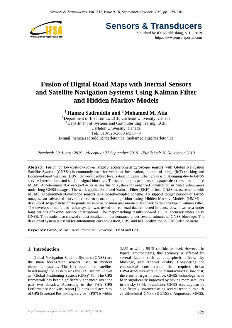
Sensors & Transducers, Vol. 237, Issue 9-10, September-October 2019, pp. 129-136
129
Sensors & Transducers
Published by IFSA Publishing, S. L., 2019 http://www.sensorsportal.com
Fusion of Digital Road Maps with Inertial Sensors and Satellite Navigation Systems Using Kalman Filter
and Hidden Markov Models
1 Hamza Sadruddin and 2 Mohamed M. Atia 1 Department of Electronics, ECE, Carleton University, Canada
2 Department of Systems and Computer Engineering, ECE, Carleton University, Canada Tel.: 613-520-2600 ex: 5779
E-mail: [email protected], [email protected]
Received: 30 August 2019 /Accepted: 27 September 2019 /Published: 30 November 2019 Abstract: Fusion of low-cost/low-power MEMS accelerometer/gyroscope sensors with Global Navigation Satellite Systems (GNSSs) is commonly used for vehicular localization, internet of things (IoT) tracking and Location-based Services (LBS). However, robust localization in dense urban areas is challenging due to GNSS service interruptions and satellite signal blockage. To overcome this problem, this paper describes a map-aided MEMS Accelerometer/Gyroscope/GNSS sensor fusion system for enhanced localization in dense urban areas under long GNSS outages. The work applies Extended Kalman Filter (EKF) to fuse GNSS measurements with MEMS Accelerometer/Gyroscope sensors in a loosely-coupled scheme. To support longer periods of GNSS outages, an advanced curve-to-curve map-matching algorithm using Hidden-Markov Models (HMM) is developed. Map-matched data points are used as position measurement feedback to the developed Kalman Filter. The developed map-aided fusion system was tested on real-road data collected in dense downtown area under long periods of GNSS service interruptions. The map-matching results showed 100 % accuracy under noisy GNSS. The results also showed robust localization performance under several minutes of GNSS blockage. The developed system is useful for autonomous cars navigation, LBS, and IoT localization in GNSS-denied areas. Keywords: GNSS, MEMS Accelerometer/Gyroscope, HMM and EKF. 1. Introduction
Global Navigation Satellite Systems (GNSS) are the main localization sensors used in modern electronic systems. The first operational satellite-based navigation system was the U.S. system known as “Global Positioning System (GPS)” [1]. The GPS framework has been significantly enhanced over the past two decades. According to the FAA GPS Performance Analysis Report [2], horizontal accuracy of GPS (Standard Positioning Service “SPS”) is within
3.351 m with a 95 % confidence level. However, in typical environments, this accuracy is affected by several factors such as atmospheric effects, sky blockage, and receiver quality. Considering the economical consideration that requires in-car GPS/GNSS receivers to be manufactured at low cost, the error is larger in practice. GNSS technology have been significantly improved by having more satellites in the sky [3-5]. In addition, GNSS accuracy can be significantly improved using several techniques such as differential GNSS (DGNSS), Augmented GNSS,
http://www.sensorsportal.com/HTML/DIGEST/P_3120.htm

Sensors & Transducers, Vol. 237, Issue 9-10, September-October 2019, pp. 129-136
130
Precise Positioning Services (PPS), or real-time kinematics (RTK). However, localization in dense urban areas is still challenging due to GNSS signals multipath or complete outage for extended periods in scenarios like tunnels and/or urban canyons. Therefore, fusion of GNSS with other sensors is a common trend that has been widely adopted.
Fusion of GNSS with self-contained dead-reckoning relative motion sensors (e.g. inertial measurement units “IMU”) such as low-cost/low-power MEMS accelerometer and gyroscope [4] sensors can bridge short GNSS outages. GNSS and accelerometer/gyroscope sensors can be fused using Extended Kalman Filter (EKF) [5]. In the fusion process, the localization state transition is triggered by IMU sensors (accelerometer and gyroscopes) while GNSS measurements are used as external observations. The observations in our case is GNSS location and speed measurements. This EKF fusion scheme is known as loosely-coupled EKF.
Although the GNSS/IMU fusion provides high-rate robust localization, the localization accuracy drifts quickly under GNSS outages leading to significant drifts as illustrated in Fig. 1. In addition, under signal reflections and refractions induced by high buildings, GNSS accuracy deteriorates leading to significantly noisy positioning as can be seen in Fig. 2. To solve these accuracy and availability problems and to provide accurate uninterrupted navigation services under these challenges, the integration of digital road maps with IMU and GNSS has been recently considered [6-7].
Road maps are currently widely available in modern car systems and high-definition (HD) [8] maps are currently being developed to enable self-driving cars and automated connected vehicles [8]. In contrast to conventional maps that human normally uses to display information, HD maps are different in the level of accuracy, comprehensiveness, resolution and details. HD maps are currently being developed on a large scale as can be seen in [9]. To support automated driving technology where positioning availability in real-time is crucial, this work proposes the integration of commercially available maps with GNSS and IMU. While digital road map network [10] is used in this paper, the same concepts are applicable to HD maps.
This work is an extension to the conference paper published by the authors in [11]. In contrast to existing map-matching methods that applies open-loop point-to-curve map projection, this work uses Hidden Markov Models (HMM) as an enhanced curve-to-curve map matching technique. According to state-of-art surveys [12], HMM is known for its accuracy in complex geometry and dense topology road networks. In addition, the proposed work applies the projected map-points as measurements update (feedback) to the developed EKF in a closed-loop map-matching scheme. This closed-loop approach provides more robust and accuracy filtering under long periods of GNSS outages.
Fig. 1. Localization error reset in GNSS Outage using Road Networks Maps.
Fig. 2. NSS errors due to multipath in urban areas. Red is GNSS and green is ground-truth solution.
2. INS/GNSS Fusion System
The vehicle’s kinematics can be modelled as dynamic system of states vector ( ) that changes over time according to the following differential equations:
( ) = ( ( ), ( )) + ( ), (1) ( ) = ℎ( ( )) + ( ), (2)
where (. )is the nonlinear dynamic model, ( ) is the stochastic system noise vector, ( )is the control signal vector, ( ) is the external measurements vector,ℎ(. )is the nonlinear measurement model and ( ) is the stochastic measurement noise vector. In this work, Kalman filter is adopted due to its real-time efficient performance [4-5]. However, Kalman filter works only under linear systems. Therefore, the differential equations in (1) and (2) must be linearized. Commonly, first order Taylor series expansion is used to obtain the following linearized system model:
( ) = ( ) ( ) + ( ), (3) ( ) = ( ) + ( ), (4) ( ) = ( ), ( ) , (5)
( ) = ℎ( ( )) (6)

Sensors & Transducers, Vol. 237, Issue 9-10, September-October 2019, pp. 129-136
131
The Kalman Filter provides optimal estimation of the error state assuming ( ) and ( ) are zero-mean Gaussian noise vectors with covariance matrices defined by:
( ) = ( ) ( ) (7) ( ) = ( ) ( ) (8)
and is the error vector with zero-mean and a covariance matrix P defined by:
( ) = ( ) ( ) (9) In discrete form, derivative can be approximated
as follows: ≈ − , (10)
where T is the sampling period. To program the filtering algorithms within a digital system, Eqs. (3) and (4) can be written in discrete form as follows:
= ( + ) + (11) = + (12) The optimal estimation of the error vector, ,
given measurements, , is calculated using two steps: prediction step
= ( , ) (13) = ( + ) ( + ) + (14)
and update step = ( + ) , (15)
= + [ − ℎ( )], (16) = ( − ) (17) In the proposed system, the vehcile’s Kinematic
model is used as the system model of Eq. (1) where the triggering control signal u(t) is the raw accelerometers and gyroscope measurements. The system states vector can be described as follows: = ( ); ( ); ; ( ); ( ) , where ( )is the position vector defined in a local navigation frame , ( ) is the velocity vector defined in local navigation frame , is the vehicle’s orientation with respect to local-level navigation frame , ( ) and ( ) are errors of accelerometers and gyroscope measurements respectively. For 3D rigid body kinematics, (. ) is a nonlinear mapping between vehicle state and control signals at time and the vehicle’s state in the next instant of time + . For a rigid body in 3D, the differential equations that describes (. ) is given by [5]:
( )( ) = ( )( ) (18) ( )( ) = ( ) ( )( ) − ( ) +( )( ) − ( ) + 2 ( ) ( )( ) (19)
( ) = ( )( )( ) − ( ) − ( ) + ( ) (20)
( ) here is the direction cosine matrix that represents the vehicle’s orientation. Rearding accelerometer and gyroscope errors, they are modeled using a Gauss-Markov random process as follows:
( ) = − ( ) + 2 ( ), (21)
( ) = − ( ) + 2 ( ), (22)
where , , and are the time constants and covariates of Gauss-Markov process [5] [5] models of accelerometer and gyroscopes biases respectively. ( ) is the trigonometric function of the vehicle’s Euler angles vector ( ) defined as 3×3 matrix: ( ) = , (23)
where
11
12
13
21
22
23
31
32
33
cos cos
cos cos sin sin cos
sin sin cos sin cos
cos sin
cos cos sin sin sin
sin cos cos sin sin
sin
sin cos
cos cos
c
c
c
c
c
c
c
c
c
θ ψφ ψ φ θ ψ
φ ψ φ θ ψθ ψφ θ φ θ ψ
φ ψ φ θ ψθ
φ θφ θ
=
= − +
= +== += − += −==
(24)
( )is the rotation rate of the local-level navigation frame with respect to the earth frame due to motion of the vehicle on the ellipsoid surface of Earth and ( )is the rotation rate of earth frame with respect to the imaginary non-rotating inertial navigation frame due to Earth’s rotation.
To avoid singularities and numerical instability, the direction cosine matrix ( ) is converted to quaternion variable ( ) = [ ] [9, 20] and the numerical integration is performed in the quaternion domain according to the following equation:
( ) = 12 ( )( )( ) − ( ) − ( ) + ( ) (25)
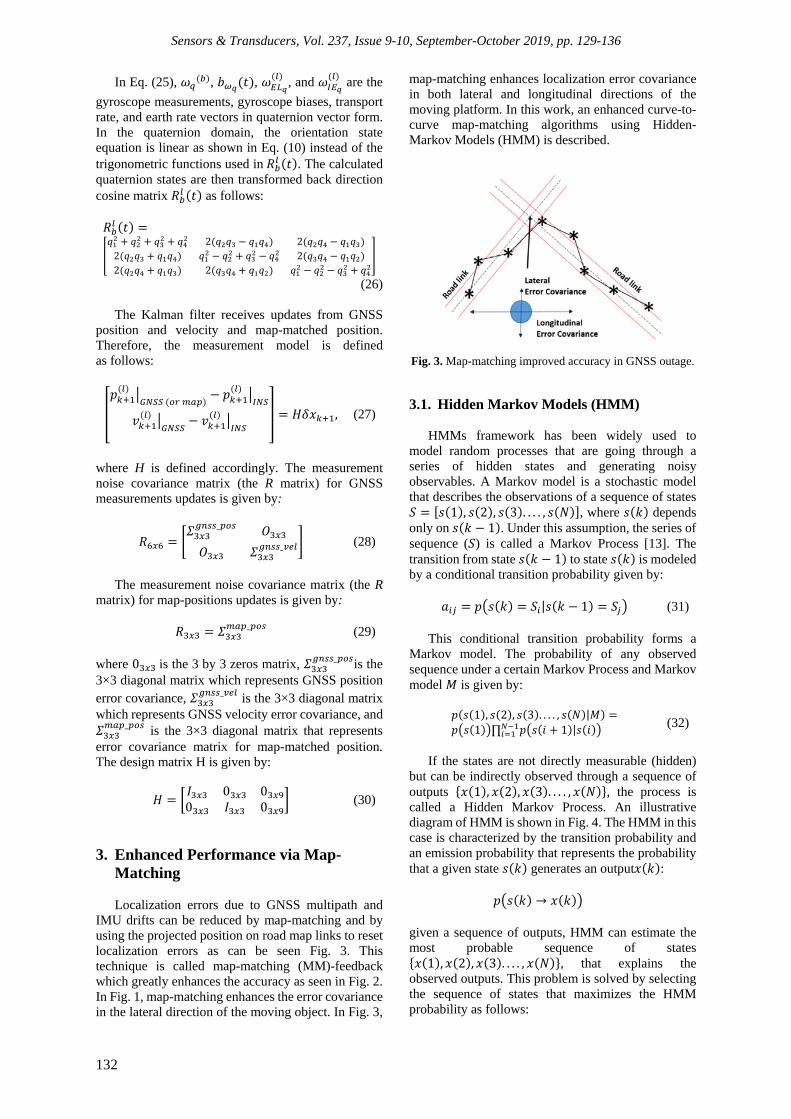
Sensors & Transducers, Vol. 237, Issue 9-10, September-October 2019, pp. 129-136
132
In Eq. (25), ( ), ( ), ( ) , and ( ) are the
gyroscope measurements, gyroscope biases, transport rate, and earth rate vectors in quaternion vector form. In the quaternion domain, the orientation state equation is linear as shown in Eq. (10) instead of the trigonometric functions used in ( ). The calculated quaternion states are then transformed back direction cosine matrix ( ) as follows:
( ) =+ + + 2( − ) 2( − )2( + ) − + − 2( − )2( + ) 2( + ) − − +
(26) The Kalman filter receives updates from GNSS
position and velocity and map-matched position. Therefore, the measurement model is defined as follows:
( ) ( ) − ( )( ) − ( ) = , (27)
where H is defined accordingly. The measurement noise covariance matrix (the R matrix) for GNSS measurements updates is given by:
= _ _ (28)
The measurement noise covariance matrix (the R
matrix) for map-positions updates is given by: = _ (29)
where 0 is the 3 by 3 zeros matrix, _ is the 3×3 diagonal matrix which represents GNSS position error covariance, _ is the 3×3 diagonal matrix which represents GNSS velocity error covariance, and _ is the 3×3 diagonal matrix that represents error covariance matrix for map-matched position. The design matrix H is given by:
= 0 00 0 (30)
3. Enhanced Performance via Map-Matching Localization errors due to GNSS multipath and
IMU drifts can be reduced by map-matching and by using the projected position on road map links to reset localization errors as can be seen Fig. 3. This technique is called map-matching (MM)-feedback which greatly enhances the accuracy as seen in Fig. 2. In Fig. 1, map-matching enhances the error covariance in the lateral direction of the moving object. In Fig. 3,
map-matching enhances localization error covariance in both lateral and longitudinal directions of the moving platform. In this work, an enhanced curve-to-curve map-matching algorithms using Hidden-Markov Models (HMM) is described.
Fig. 3. Map-matching improved accuracy in GNSS outage.
3.1. Hidden Markov Models (HMM) HMMs framework has been widely used to
model random processes that are going through a series of hidden states and generating noisy observables. A Markov model is a stochastic model that describes the observations of a sequence of states = [ (1), (2), (3). . . . , ( )], where ( ) depends only on ( − 1). Under this assumption, the series of sequence ( ) is called a Markov Process [13]. The transition from state ( − 1) to state ( ) is modeled by a conditional transition probability given by:
= ( ) = | ( − 1) = (31) This conditional transition probability forms a
Markov model. The probability of any observed sequence under a certain Markov Process and Markov model is given by:
( (1), (2), (3). . . . , ( )| ) =(1) ∏ ( + 1)| ( ) (32)
If the states are not directly measurable (hidden)
but can be indirectly observed through a sequence of outputs (1), (2), (3). . . . , ( ) , the process is called a Hidden Markov Process. An illustrative diagram of HMM is shown in Fig. 4. The HMM in this case is characterized by the transition probability and an emission probability that represents the probability that a given state ( ) generates an output ( ):
( ) → ( )
given a sequence of outputs, HMM can estimate the most probable sequence of states (1), (2), (3). . . . , ( ) , that explains the observed outputs. This problem is solved by selecting the sequence of states that maximizes the HMM probability as follows:

Sensors & Transducers, Vol. 237, Issue 9-10, September-October 2019, pp. 129-136
133
= ∈ ( ), ( ),... ( ) (1) → (1) ∏ ( + 1)| ( )( + 1) → ( + 1) (33)
Fig. 4. Markov Process Diagram.
HMM estimation method is called “decoding” and it is solved using the Viterbi Algorithm [14]. In the proposed system, the hidden states represent map links and the observable outputs are the vehicle poses. To develop a robust map-matching framework, the vehicle pose history, roads geometry, and map topology constraints must be considered. Therefore, the emission and transition probabilities of a HMM are formulated such that they reflect all the aforementioned constraints. The HMM-based framework is illustrated in Fig. 5. The emission probabilities are calculated as follows:
= ∑ ∈ , (34)
where is the set of all map segments within 50 m distance from current vehicle position in the ith epoch. The weighting parameter is calculated as follows:
= + ‖ ‖ , (35)
where is the distance from the vehicle’s estimated position in the ith epoch and its projection on the lth map segment. is the normalized angle difference between the vehicle’s estimated heading in the ith epoch and the heading of the lth map segment. The parameters A, a, B, and b are constants chosen to achieve balanced weighting that considers both distance and direction of motion consistency. The transition probabilities are calculated as follows:
= ∑ ∈ , (36)
where is the probability of transition from lth map link to mth map link given the vehicle’ position at epochs i and j respectively. is the set of all map links
connected to lth map link. The weighting parameter is calculated as follows
= , (37)
where is the normalized angle difference between the vehicle’s estimated heading in the ith and jth epochs, is the normalized angle difference between the heading of the lth and mth map segments and is the connectivity parameter that determines if map segments lth and mth are topologically connected and c is a constant parameter.
In our proposed system, the possible road network map segments were represented as hidden states, whereas the vehcile’s location was an observable state. In this case, vehicle’s dynamics and road network topology are used to build transition probability matrix while emission probabilities represented the probability that a given state (i.e. road segment) generates an output (vehicle’s location). Fig. 3 shows how the problem is modeled as a HMM. Viterbi Algorithm [3] was used to find the sequence of road map segments that most likely to have generated the observed locations. To develop a robust map-matching framework, the vehicle location and orientation history, roads geometry, and map topology constraints were considered in calculating emission and transition probabilities. Fig. 6 shows the system components.
Fig. 5. Map-matching as HMM.
Fig. 6. Overall System Block Diagram.
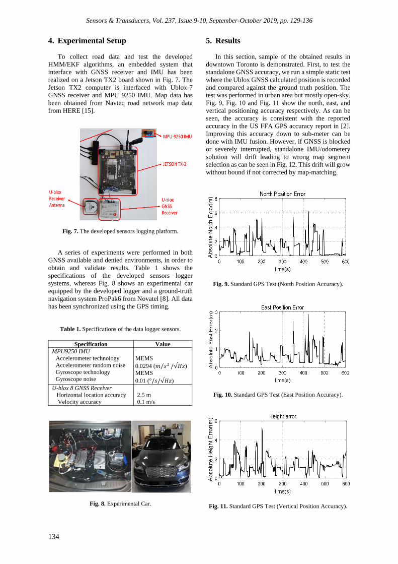
Sensors & Transducers, Vol. 237, Issue 9-10, September-October 2019, pp. 129-136
134
4. Experimental Setup To collect road data and test the developed
HMM/EKF algorithms, an embedded system that interface with GNSS receiver and IMU has been realized on a Jetson TX2 board shown in Fig. 7. The Jetson TX2 computer is interfaced with Ublox-7 GNSS receiver and MPU 9250 IMU. Map data has been obtained from Navteq road network map data from HERE [15].
Fig. 7. The developed sensors logging platform.
A series of experiments were performed in both GNSS available and denied environments, in order to obtain and validate results. Table 1 shows the specifications of the developed sensors logger systems, whereas Fig. 8 shows an experimental car equipped by the developed logger and a ground-truth navigation system ProPak6 from Novatel [8]. All data has been synchronized using the GPS timing.
Table 1. Specifications of the data logger sensors.
Specification Value
MPU9250 IMU Accelerometer technology Accelerometer random noise Gyroscope technology Gyroscope noise
MEMS 0.0294 ( ⁄ /√ ) MEMS 0.01 (°/ /√ )
U-blox 8 GNSS Receiver Horizontal location accuracy Velocity accuracy
2.5 m 0.1 m/s
Fig. 8. Experimental Car.
5. Results In this section, sample of the obtained results in
downtown Toronto is demonstrated. First, to test the standalone GNSS accuracy, we run a simple static test where the Ublox GNSS calculated position is recorded and compared against the ground truth position. The test was performed in urban area but mostly open-sky. Fig. 9, Fig. 10 and Fig. 11 show the north, east, and vertical positioning accuracy respectively. As can be seen, the accuracy is consistent with the reported accuracy in the US FFA GPS accuracy report in [2]. Improving this accuracy down to sub-meter can be done with IMU fusion. However, if GNSS is blocked or severely interrupted, standalone IMU/odometery solution will drift leading to wrong map segment selection as can be seen in Fig. 12. This drift will grow without bound if not corrected by map-matching.
Fig. 9. Standard GPS Test (North Position Accuracy).
Fig. 10. Standard GPS Test (East Position Accuracy).
Fig. 11. Standard GPS Test (Vertical Position Accuracy).

Sensors & Transducers, Vol. 237, Issue 9-10, September-October 2019, pp. 129-136
135
Fig. 12. IMU/odometer solution drift leading to wrong map segment selection. The circle indicates the start of the GNSS outage, and the rectangle indicates the drift that
leads to wrong map segment selection.
Fig. 13 and Fig. 14 demonstrate the benefit of the described HMM-based map-matching fusion. As can be seen in the figures, map-aided solution successfully identifies the map segment on which the vehicle is moving on.
Fig. 13. Map-matching in an intersection. Map aided solution is in yellow shows the correct track while red
curves show the road map network.
Fig. 14. Map-matching in an exit. Map aided solution is in yellow shows the correct track while red curves show
the road map network.
The accuracy is demonstrated under challenging road network intersection with a bridge (Fig. 13) and in a high-way exit fork (Fig. 14). Table 2 shows the localization error under four 60-seconds GNSS outages with and without the developed map-aided fusion system. During the outage, only IMU is used without any additional measurements from the car speed measurements or non-holonomic constrains.
To test long GNSS outage, a simulated GNSS outage of 20 minutes has been tested. As can be seen from Fig. 15, the system sustained reliable map-matching and enhanced accuracy for the entire 20 minutes with a sub-meter overall localization error.
Table 2. The localization error under four 60-seconds GNSS outages with and without the developed map-aided
fusion system.
2D horizontal error (m) without map-matching (IMU odometry only, no
GNSS, non-holonomic constraints, no speed measurements)
Outage 1
Outage 2
Outage 3
Outage 4
RMSE 19.73 19.05 18.64 18.84 Max Error
44.61 37.34 38.44 41.21
2D horizontal error (m) with map-matching (IMU odometry only plus
HMM map feedback) Outage
1Outage
2Outage
3 Outage
4RMSE 0.65 0.79 0.45 0.69 Max Error
1.78 1.62 1.69 1.83
Fig. 15. Improved accuracy in long GNSS outage in Downtown area (20 minutes).
6. Conclusion This work introduced an enhanced HMM-based
map-aided IMU/GNSS sensor fusion system on an embedded platform. HMM has been shown to be a robust and accurate map-matching framework that can support continuous navigation for long periods of GNSS outages. An outage of 20 minutes has been tested with sub-meter positioning accuracy and 100 % map segment selection accuracy has been achieved.
Sensors & Transducers, Vol. 237, Issue 9-10, September-October 2019, pp. 129-136
136
By introducing this proposed implementation of HMM-based map-matching IMU/GNSS fusion, this work will open the door for a new generation of robust and efficient localization systems that will enable several emerging applications such as self-driving cars and internet of things. Although segment-based road network maps have been used in this work, the concept is applicable to emerging HD maps to enable self-driving cars to navigate in GNSS-denied and challenging areas. References [1]. P. Misra, P. Enge, Global Positioning System, Signals,
Measurements, and Performance, Ganga-Jamuna Press, 2011.
[2]. William J. Hughes Technical Center, Global Positioning System (GPS), Standard Positioning Service (SPS), Performance Analysis Report #86, William J. Hughes Technical Center, NSTB/WAAS T&E Team, July 31, 2014.
[3]. A. El-Rabbany, Introduction to GPS: The Global Positioning System, Second Edition, Artech House, 2006.
[4]. J. Farrell, Aided Navigation: GPS with High Rate Sensors, McGraw-Hill, New York, 2008.
[5]. P. D. Groves, Principles of GNSS, Inertial, and Multisensor Integrated Navigation Systems, Artech House, 2013.
[6]. R. Toledo, D. Betaille, F. Peyret, J. Laneurit, Fusing GNSS, Dead-Reckoning, and Enhanced Maps for Road Vehicle Lane-Level Navigation, IEEE Journal of Selected Topics in Signal Processing, Vol. 3, Issue 5, 2009, pp. 798-809.
[7]. R. Toledo, D. Betaille, F. Peyret, Lane-Level Integrity Provision for Navigation and Map Matching With GNSS, Dead Reckoning, and Enhanced Maps, IEEE Transactions on Intelligent Transportation Systems, Vol. 11, Issue 1, 2010, pp. 100-111.
[8]. H. G. Seif, X. Hu, Autonomous Driving in the iCity—HD Maps as a Key Challenge of the Automotive Industry, Elsevier, Engineering, Vol. 2, Issue 2, June 2016, pp. 159-162.
[9]. S. Niijima, J. Nitta, Y. Sasaki, H. Mizoguchi, Generating 3D fundamental map by large-scale SLAM and graph-based optimization focused on road center line, in Proceedings of the 26th IEEE International Symposium on Robot and Human Interactive Communication (RO-MAN), Lisbon, Portugal, September 2017.
[10]. M. M. Atia, A. R. Hilal, C. Stellings, E. Hartwell, J. Toonstra, W. B. Miners, O. A. Basir, A Low-Cost Lane-Determination System Using GNSS/IMU Fusion and HMM-Based Multistage Map Matching, IEEE Transactions on Intelligent Transportation Systems, Vol. 18, Issue 11, 2017, pp. 3027-3037.
[11]. H. Sadruddin, M. M. Atia, Real-time Fusion of MEMS Accelerometers/Gyroscopes with Global Navigation Satellite Systems and Road Networks for Enhanced Urban Localization, in Proceedings of the 5th
International Conference on Sensors and Electronic Instrumentation Advances (SEIA'19), Tenerife (Canary Islands), Spain, 25-27 September 2019, pp. 153-156.
[12]. M. R. Manikandan, Dr. R. Latha, A Literature Survey of Existing Map Matching Algorithms for Navigation Tehcnology, International Journal of Engineering Sciences & Research Technology, Vol. 6, Issue 9, 2017, pp. 326-331.
[13]. R. J. Elliott, L. Aggoun, J. B. Moore, Hidden Markov Models: Estimation and Control, Springer, Business & Economics, 1995.
[14]. L. K. Balivada, K. P. Raju, Optimization Techniques of Viterbi Algorithm: Performance Analysis of Different Algorithms, LAP LAMBERT Academic Publishing, 11 May 2012.
[15]. HERE, [Online], https://company.here.com/here/ [Accessed 19 January 2016].
[16]. P. G. Savage, Strapdown Analytics - Second Edition, Strapdown Associates, Inc., Minnesota, USA, 2000.
__________________
Published by International Frequency Sensor Association (IFSA) Publishing, S. L., 2019 (http://www.sensorsportal.com).

Sensors & Transducers, Vol. 237, Issue 9-10, September-October 2019, pp. 137-143
137
Sensors & Transducers
Published by IFSA Publishing, S. L., 2019 http://www.sensorsportal.com
Molecular Dynamics Simulation on Formation of Ge Thin Film for Flexible Communication Devices
* Yoshiaki KOGURE, Tomoko FUNAYAMA and Yasutaka UCHIDA
Teikyo University of Science Adachi-ku, Tokyo, Japan Tel.: + 81-47-411-6265
* E-mail: [email protected]
Received: 30 August 2019 /Accepted: 27 September 2019 /Published: 30 November 2019 Abstract: Materials for flexible sensor that operate in close contact with the skin has been investigated. The sensor maintain the quality of life and the communication device for disabled people. Low-temperature crystallization and mechanical properties of Germanium thin films have been simulated by means of molecular dynamics under free boundary condition. Tersoff bond order potential was adopted for calculating the interactions between germanium atoms. Amorphous model was prepared by quenching the molten system at 1800 K. The model was consisted of 10,500 atoms. By annealing the amorphous state at 400 K, partial crystallization was realized. Crystallization was verified by the radial distribution function of the model. Then the film was deformed and stress-strain relation was calculated. The change of atomic structure during the deformation was investigated from the cross-sectional views. The mechanical strength and flexibility are discussed from microscopic point of view. Simulation plays a complementally role with the experimental research and contributes to the development of the flexible sensors. Keywords: Germanium thin film, Molecular dynamics, Tersoff potential, Crystallization, Stress-strain relation, Flexible sensor, Communication device. 1. Introduction
A flexible sensor that functions closely to the skin is an indispensable tool in the field of care and rehabilitation. Recently, it has become possible to measure the vital signs for a long time. In order to be able to measure in daily life, it is necessary to have a flexible sensor that can be deformed according to the shape of skin. Resetting is required when a gap appears between sensor and skin. Stable sensor operation is really required. We have been studying hemoglobin measurement as a communication device for disabled people. Such a device employs near-infrared spectroscopy (NIRS) [1]. The fabrication of sensors that adhere to the skin is essential to accurately
measure the oxyhemoglobin in the blood flow. The present authors have been engaged in the study to fabricate the germanium thin films on the flexible substrates in the project to improve the yes/no device [2-3]. The low-temperature metal-induced poly-crystallization of electrodeposited germanium thin film on flexible substrate has been realized experimentally. Germanium has a high carrier mobility and low processing temperature. In our experimental study germanium films are deposited at 60oC and crystallized at 150oC (423 K). However, the microscopic process of the mechanism of crystallization is not well understood in many cases [4-5]. Molecular dynamics simulation is a powerful way to visualize microscopic processes of
http://www.sensorsportal.com/HTML/DIGEST/P_3121.htm
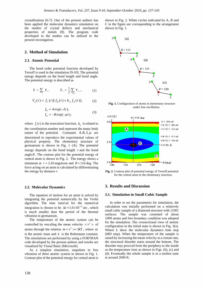
Sensors & Transducers, Vol. 237, Issue 9-10, September-October 2019, pp. 137-143
138
crystallization [6-7]. One of the present authors has been applied the molecular dynamics simulation on the studies of crystal defects and mechanical properties of metals [8]. The program code developed in the studies can be utilized in the present investigation.
2. Method of Simulation
2.1. Atomic Potential The bond order potential function developed by
Tersoff is used in the simulation [9-10]. The potential energy depends on the bond length and bond angle. The potential energy is described as
,
1, ,
2i i i ji j i
E E E V≠
= = (1)
C R A( ) ( )[ ( ) ( )],ij ijV r f r f r b f r= + (2)
R
A
exp( ),
exp( ).
f A r
f B r
λμ
= −= − − ,
(3)
where ( )cf r is the truncation function, ijb is related to
the coordination number and represent the many body nature of the potential. Constants , , ,A B λ μ are
determined to reproduce the experimental values of physical property. The elementary structure of germanium is shown in Fig. 1 (A). The potential energy depends on the bond length r and the bond angleθ . The contour plot for the potential energy of central atom is shown in Fig. 2. The energy shows a minimum at 2.43r = angstrom and 116θ = deg. The force acting on an atom is calculated by differentiating the energy by distance r.
2.2. Molecular Dynamics
The equation of motion for an atom is solved by integrating the potential numerically by the Verlet algorithm. The time interval for the numerical integration is chosen to be 151.0 10 sect −Δ = × , which is much smaller than the period of the thermal vibration in germanium.
The temperature of the atomic system can be controlled by rescaling the mean velocity 2v< > of
atoms through the relation 2 3m v kT< >= , where mis the atomic mass and k is the Boltzmann constant. The simulations are performed by using a FORTRAN code developed by the present authors and results are visualized by Visual Basic (Microsoft).
As a simplest simulation, snapshots in free vibration of three atomic system in shown in Fig. 1. Contour plot of the potential energy for central atom is
shown in Fig. 2. White circles indicated by A, B and C in the figure are corresponding to the arrangement shown in Fig. 1.
Fig. 1. Configuration of atoms in elementary structure under free oscillation.
Fig. 2. Contour plot of potential energy of Tersoff potential for the central atom in the elementary structure.
3. Results and Discussion 3.1. Simulation in Small Cubic Sample
In order to set the parameters for simulation, the calculation was initially performed on a relatively small cubic sample of a diamond structure with 100 surfaces. The sample was consisted of about 1000 atoms and free boundary condition was adopted for the simulation. The crossectional view of atomic configuration in the initial state is shown in Fig. 3(a). Where L show the molecular dynamics time step (MD step). When the temperature of the sample is raised by increasing the mean velocity at a certain rate, the structural disorder starts around the bottom. The disorder may procced from the periphery to the inside as the temperature rises as shown in Figs. (b), (c) and (d). Eventually the whole sample is in a molten state at around 2000 K.

Sensors & Transducers, Vol. 237, Issue 9-10, September-October 2019, pp. 137-143
139
Fig. 3. Configuration of atoms in cubic sample during heating.
Four atoms in the vicinity of the center were selected as sample atoms. Trajectories of those atoms during the temperature rise are shown in Fig. 4 (a). The zigzag trajectory appears to be due to the diffusion of atoms in the molten state. Fig. 4 (b) shows the temperature change with respect to the simulation step (time). It can be seen that the temperature rises to around 2000 K at a constant rate and then controlled to be constant. The displacements from the starting points of sample atoms are plotted against the time step in Fig. 4 (c). The colour coding of sample atom is the same as Fig. (a). In the first half of the simulation, the sample atoms are hardly moving, but when they reach a certain temperature, they start moving all at once. Its temperature is 1250 K, close to the melting temperature of Ge. That is, it can be seen that not only static structure but also the sample is melted dynamically.
Fig. 4. Trajectory and displacement of sample atoms during heating (a), time variation of sample temperature (b),
and displacements from initial positions.
Fig. 5 shows histograms of the velocity distributions of atoms in the specimen being heated. As is well known, the velocity in thermal equilibrium follows the Maxwell distribution
3/2 22( ) 4 exp
2 2
m mvf v v
kT kTπ
π = −
(4)
The solid lines in the figure show the calculated Maxwell distribution for each temperature. In the simulation, the initial velocity given to the atoms is generated by a uniform random number. As the simulation proceeds, it can be seen that the velocity distribution approaches the Maxwell distribution.
Fig. 5. Velocity distribution of atoms at elevated temperatures.
3.2. Crystallization of Cubic Sample
When a sample in a molten state is rapidly cooled, an amorphous state appears. This is a state where a disordered atomic arrangement in a liquid state is frozen. Fig. 6(a) shows an amorphous state produced by quenching the molten state shown in Fig. 3(d). The radial distribution function is shown on the right side. A sharp peak is observed around 2,5 angstrom, followed by irregular fluctuations.
It is known that atomic configuration in an amorphous state is unstable and crystallizes at a relatively low temperature. Fig. 6(b) and (c) show the process of crystallization at around 400 K. In Fig. 6(b), it can be seen that crystallization has started in the area indicated by A and B. Furthermore, when the simulation is continued at that temperature, crystallization progresses, and it can be seen that the whole sample approaches one single crystal. The external shape of the sample shows a crystal shape surrounded by linear planes, and the radial distribution function has a pulse shape, which is also characteristic of crystal.
3.3. Formation of Thin Film Sample
Thin film samples for the simulation is consisted of 10,500 atoms. In the initial state, atoms are arranged in a perfect crystal of diamond structure of rectangular shape with 100 faces. The size is 9 nm×9 nm×3 nm, as shown in Fig. 7(a), where the nearest neighbor atoms are connected by straight lines.

Sensors & Transducers, Vol. 237, Issue 9-10, September-October 2019, pp. 137-143
140
(a) Initial crystal
(b) Molten state
(c) Amorphous state
Fig. 6. Crystallization of cubic sample from amorphous state.
Fig. 7. Preparation of amorphous sample.
Then the temperature is raised to 1900 K or more
to bring it into a molten state (Fig. 7(b)). The atoms in the system of molten state are in completely disordered state. After keeping in the molten state for 30,000 MD steps the system is suddenly quenched to 0 K, and then the amorphous state is realized as shown in Fig. 7(c). The temperature variation during the amorphization process is shown as a function of MD step in Fig. 8. The temperature in molten state is seen to be controlled flat and suddenly drops to 0 K.
Fig. 8. Temperature variation during amorphorization.
3.4. Crystallization of Thin Film at 400 K
In the experimental study, Cu-induced poly-crystallization of electrodeposited films were observed at 150 oC (423 K). The molecular dynamics simulations for annealing and crystallization in large thin film (10,500 atoms) samples were performed at 400 K, where the metal element was not involved. Two types of boundary conditions between the sample and the substrate were tried.
1) The substrate and the sample are in closely contacted and atoms can slide on the surface.
2) The sample is loosely contacted with the substrate allowing a gap within 10 angstrom.
In the boundary condition 1), crystallization has hardly progressed because atoms are mostly fixed at the lower end. On the contrary, in the boundary, condition 2), it can be seen that polycrystallization is more advanced because of the boundary close to the free surface even at the lower end. An example of crystallization at the substrate is shown in Fig. 9. A progress of crystallization at the left side is seen. In order to occur a crystallization, a degree of freedom in the three-dimensional direction may be necessary at

Sensors & Transducers, Vol. 237, Issue 9-10, September-October 2019, pp. 137-143
141
the surface. Namely, the boundary condition is very important for the crystallization of thin films.
Atomic structure in a plane parallel to the bottom of thin film is shown in Fig. 11. It is a heterogeneous structure of crystalline and amorphous parts. The radial distribution (RDF) at typical zones (A), (B), (C) are inserted in the figure. RDF in regions (A) and (B) show crystalline character, but RDF in (B) is sharper and has shown higher crystallinity than (A). RDF in (C) shows disordered and amorphous nature.
Judging from Fig. 9 and Fig. 11, the characteristic sizes of the crystalline and amorphous regions appear to be comparable to the thickness of thin film. Typical time steps of the molecular dynamics is 100,000.
Meanwhile the outershape and the heterogeneous structure of films were changing. The average potential energy of atoms increased once, and decreased again. At that time, a change in heterogeneous structure was observed. Simulation at a different temperature, 500 K, was performed, and similar behavior was seen. The movement of atoms was more intense when the temperature was higher.
Fig. 10 show the change in potential energy of small cubic sample and large thin film sample during the crystallization processes. In the cubic sample, energy decreases monotonically and crystallization progresses, whereas in the thin film sample, energy decreases slowly while increasing and decreasing repeatedly. In the thin film sample, crystallization begins in each part, and it seems that the growth of grain boundaries with different orientations pushing each other. The smaller cubic sample has higher potential energy per atom because the proportion of atoms present on the sample surface is large.
Fig. 9. Crystallization near substrate under loosely contacted boundary condition.
Fig. 10. Change of potential energy in cubic and thin film samples.
Fig. 11. Annealed thin film sample and radial distribution functions.
3.5. Mechanical Properties
Tensile and compression stresses were applied on the thin film sample. The atomic configuration during deformation is shown in Fig. 12, where the atoms shown by red circles are rigidly displaced in opposite directions to apply the tensile and compression strains. The strain rate is 91.6 10 / sec× and maximum strain
is about 8 %. The stress can be calculated from the sum of the forces acting on fixed atoms during deformation. In fact, since the forces acting on atoms inside the fixed region cancel each other. Only the forces at the boundary remain and contribute to the stress. Calculated stress-strain relation is shown in Fig. 13.

Sensors & Transducers, Vol. 237, Issue 9-10, September-October 2019, pp. 137-143
142
Fig. 12. Atomic structure in tensile (a) and compression (b) deformation. Shown on the right of each figure are the atomic arrangements of the cross-section cut along the A, B and C planes.
Fig. 13. Stress-strain relations in tensile (a) and compression (b) deformation.
The stress is seen to be increasing in proportion to the strain in the first part of the stress-strain relation in Fig. 13. Young’s modulus may be able to be estimated as 3 GPa, which is much smaller than the perfect crystal of germanium. This may be due to the sparse structure of present sample. The stress approaches a constant value at a strain of 4 % or more. The atomic structure during deformation is a mixture of crystalline parts and amorphous disordered structures as shown in Fig. 12. The mosaic structure changes as the deformation progressed. The mechanism of deformation of this thin film seems to be similar to the deformation of polycrystals by slippage of grain boundaries. The motion of dislocations and other point defects might be concerned.
4. Possibility for Flexible Devices
In recent years, interest in bending and expanding material has increased in the healthcare field for vital
sensing. In general, a flexible material such as a polymer has no heat resistance, and it is desirable that an amorphous semiconductor deposited thereon is crystallized at a relatively low temperature. Ge that crystallizes at about 400 K (130 oC) is a suitable material. Recently, the appearance of 1 – 2 nm clusters during Ge crystallization was discovered by a transmission electron microscope and attracting attention. The present study seems to be effective in elucidating the micro process. 5. Conclusions
Low temperature crystallization of germanium thin
film has been simulated by means of molecular dynamics using Tersoff potential. In particular, the movement of individual atoms at the interface with the substrate was found to be important. This point is really helpful in the experimental study. The

Sensors & Transducers, Vol. 237, Issue 9-10, September-October 2019, pp. 137-143
143
heterogeneous structure consist of crystalline and amorphous regions was realized. Basic calculation on the mechanical properties of germanium thin films were also made. The stress-strain relation of heterogineeous film was successfully delivered by the simulation. The analysis of flexible natures of sensors linked to actual skin movement is difficult because the models that can be handled by molecular dynamics are too small. Adoption of multiscale model combining atomic model with continuum model seems to be effective.
Present study explore the communication possibility of disabled people. The accuracy of measurement indoor life has increased. However it may not be used outdoors with heavy activity, because the device still lacks flexibility and stability. References [1]. M. Naito, Y. Michioka, K. Ozawa, I. Ito, M. Kiguchi,
T. Kanazawa, A communication means for totally locked-in ALS patients based on changes in cerebral blood volume measured with near-infrared light, IEICE Transactions on Information and Systems, Vol. E90-D, Issue 7, 2007, pp. 1028-1037.
[2]. Y. Uchida, T. Funayama, Y. Kogure, W. Yeh, Metal-induced low-temperature crystallization of electrodeposited Ge yjin film, Japanese Journal of Applied Physics, Vol. 55, Issue 3, 2016, pp. 031303-1–031303-5.
[3]. Y. Uchida, T. Funayama, Y. Kogure, W. Yeh, Low-temperature Cu-induced poly-crystallization of
electrodeposited germanium thin film on flexible substrate, Physica Status Solodi C, Vol. 13, Issue 10-12, 2016, pp. 864-867.
[4]. D. Shahrjerdi, B. Hekmatshoar, S. S. Mohajerzadeh, A. Khakifirooz, M. Robertson, High Mobility Poly-Ge Thin-Film Transistors Fabricated on Flexible Plastic Substrates at Temperatures below 130o C, Journal of Electronic Materials, Vol. 33, Issue 4, 2004, pp. 353-357.
[5]. W. Knaepen, S. S. Gaudet, C. Detavernir, R. L. Van Meirrhaeghe, J. Jordan Sweet, C. Lavoie, In situ x-ray diffraction study of metal induced crystallization of amorphous germanium, Journal of Applied Physics, Vol. 105, Issue 8, 2009, pp. 083532-1–083532-7.
[6]. Y. Kogure, T. Funayama, Y. Uchida, Atomistic Simulation of Structure and Dynamics in Crystallizing Germanium Thin Films, Sensors & Transducers, Vol. 227, Issue 11, November 2018, pp. 21-27.
[7]. Y. Kogure, T. Funayama, Y. Uchida, Simulation of Crystallization and Mechanical Properties of Ge Thin Film for Flexible sensor in Communication Devices, in Proceedings of the 5th International Conference on Sensors and Electronic Instrumentation Advances (SEIA’ 2019), Tenerife (Canary Islands), Spain, 25-27 September 2019, pp. 88-91.
[8]. Y. Kogure, Y. Hiki, Atomistic Simulation of Shear Mode Deformation of Nanocrystalline Copper with Different Grain Sizes, Materials Transactions, Vol. 55, Issue 1, 2014, pp. 64-68.
[9]. J. Tersoff, New empirical approach for the structure and energy of covalent systems, Physical Review B, Vol. 37, Issue 12, 1988, pp. 6991-7000.
[10]. J. Tersoff, Modeling solid-state chemistry: interatomic potential for multicomponent systems, Physical Review B, Vol. 39, Issue 8, 1989, pp. 5566-5568.
__________________
Published by International Frequency Sensor Association (IFSA) Publishing, S. L., 2019 (http://www.sensorsportal.com).

Sensors & Transducers, Vol. 237, Issue 9-10, September-October 2019, pp. 144-149
144
Sensors & Transducers
Published by IFSA Publishing, S. L., 2019 http://www.sensorsportal.com
ZigBee-Based Wireless Sensor Network for Environment Monitoring ZigBee
1, # Fuzheng Zhang, 2, # Weile Jiang, 1, 3, 4, 5, * Qijing Lin, 1 Hao Wu
1 State Key Laboratory for Manufacturing Systems Engineering, Xi’an Jiaotong University, 710049, Xi’an, China
2 Institute of Heritage Sites & Historical Architecture Conservation, Xi’an Jiaotong University, Xi’an, 710049, China
3 Collaborative Innovation Center of High-End Manufacturing Equipment, Xi'an Jiaotong University, Xi’an, 710054, China
4 Xi’an Jiaotong University Suzhou Institute, Suzhou, 215123, China 5 State Key Laboratory of Mechanical System and Vibration, Shanghai Jiaotong University,
Shanghai, 200240, China * Tel.: + 862982668616
* E-mail: [email protected]
Received: 30 August 2019 /Accepted: 27 September 2019 /Published: 30 November 2019 Abstract: ZigBee technology with the characteristics of low complexity, ad-hoc network, low cost, low power consumption and high security, is widely used for wireless sensing. Wireless sensor network is an interdisciplinary application between multi-sensor technology and wireless network, and has the broad application prospects in many fields such as intelligent agriculture and smart home. This paper designs and realizes an indoor environment monitoring system based on ZigBee and wireless sensor network. The system uses end-nodes to collect temperature, humidity, PM2.5 and other environmental parameters. The collected data is transmitted to the coordinator through wireless sensor network and finally to the monitoring system software by serial port protocol. The online monitoring platform with functions of real-time data display, storage and over-limit warning is developed by using the LabVIEW software. The test results show that the system is stable, easy to generate a network system, speedy and reliable to transmit data, and flexible to place nodes. Keywords: ZigBee, Wireless sensor network, Environment monitoring, LabVIEW, Monitoring platform.
1. Introduction Based on the characteristics of high information
integration and multi-disciplinary intersection, Wireless Sensor Network (WSN) is concerned by various countries. SN involves embedded computer technology, communication technology, sensor technology and distributed information processing technology. It can collect various environmental parameters in the area covered by the wireless network, and process the information accordingly, and
finally transmit them to the users who need the information [1]. At present, the network protocols applied to WSN mainly include Wireless Fidelity (WiFi), Bluetooth, General Packet Radio Service (GPRS), ZigBee, etc. Among them, ZigBee technology has the advantages of low complexity, self-organizing network, low cost, low power consumption and high security. It is widely used in smart agriculture [2-6], smart home [7-9], chemical detection [10-13], medical rehabilitation [14-17] and Smart factory [18-23].
http://www.sensorsportal.com/HTML/DIGEST/P_3122.htm

Sensors & Transducers, Vol. 237, Issue 9-10, September-October 2019, pp. 144-149
145
In recent years, ZigBee technology, because of its superiority, has been used for environmental monitoring [2-23]. Zhang, et al. [5] designed an intelligent control system for the environmental monitoring in greenhouses. This system realizes the monitoring of environmental parameters in greenhouses, e.g., temperature and humidity. However, the type of sensors used is single and the number of nodes is too large; Gong, et al. [9] designed an environment monitoring system in smart home based on ZigBee. This system has the advantage of the real-time monitoring. However, the parameters monitored by the system are few and the software lacks the functions of data storage and over-limit warning. In addition, the package of nodes has not been designed; Ni, et al. [14] studied a telemedicine system based on ZigBee, EDGE, Ethernet and embedded LINUX system. This system realizes the functions of home self-care, remote diagnosis, etc., but the system is too complicated. Castro, et al. [18] described the development of an industrial automation system based on a ZigBee wireless sensor network, designed for the monitoring and control of multiple refrigeration equipment in an industrial area, replacing the existing cabled network, which was based on the LonWorks platform. However, the functionality of the system is relatively simple and the accuracy of the control is relatively low. At present, most researches on ZigBee technology are only applied to specific occasions, i.e., it is not universal.
This study aims to realize indoor environment monitoring with the characteristics of low complexity, ad-hoc network, low cost, low power consumption and high security. In order to avoid the problems of
complicated wiring, poor mobility, high cost and energy loss caused by traditional optical fiber, coaxial cable and other wired monitoring, this study designed and built an environmental monitoring system based on ZigBee technology. The system can effectively reduce the number of nodes and improve the utilization of nodes. This paper developed a new type of terminal node package box to achieve waterproof and dustproof protection for node modules. The online monitoring platform for this system was developed by LabVIEW software to realize data display, storage and over-limit warning of the collected indoor environmental data.
2. Monitoring System Design
2.1. System Design As shown in Fig. 1, the monitoring system is
mainly composed of three parts: a terminal node, a coordinator and an online monitoring platform. All the sensors are installed on the terminal node. The acquired environmental data by the terminal node is wirelessly transmitted to the coordinator module and finally sent to the monitoring platform. If the distance between the terminal node and the coordinator is too far to achieve effective transmission, power amplifiers can be used to extend the transmission distance. The system layout is shown in Fig. 2. The coordinator is connected to the PC by a USB cable. In addition, the terminal node and coordinator are identical in hardware. They are only different in functions by burning different codes.
Fig. 1. System framework.
Fig. 2. System layout.
2.2. Network Topology and Sensor Parameters
In the ZigBee protocol specification, three network topologies are defined: star structure, tree structure and mesh structure. Among the three network topologies, the star structure is the simplest one. As shown in Fig. 3, there is no router in the star structure, only one coordinator and multiple terminal nodes, and all terminal nodes are required to be within the communication range of the coordinator. That is, the star structure is a radial system, and all devices communicate with the coordinator at the center. If any two terminal nodes need to communicate with each other, one of the nodes is required to send data to the
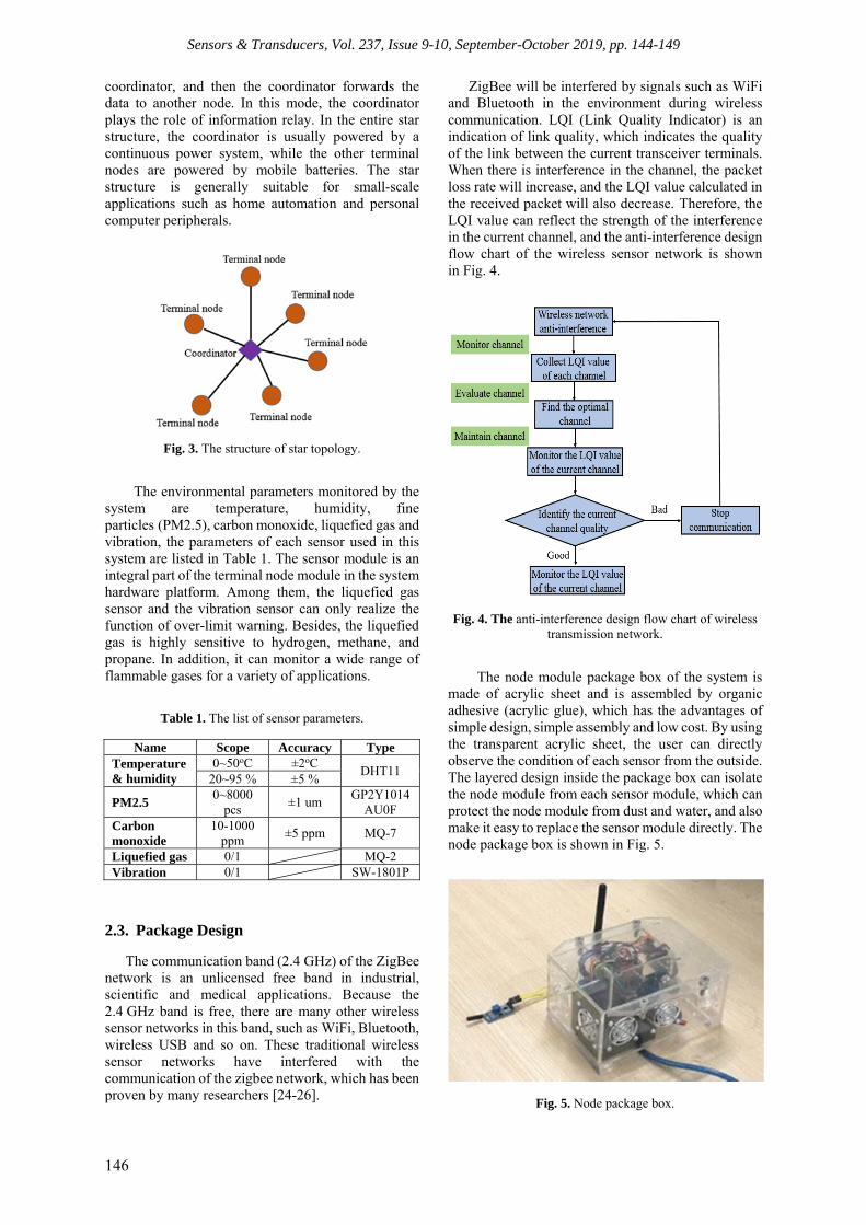
Sensors & Transducers, Vol. 237, Issue 9-10, September-October 2019, pp. 144-149
146
coordinator, and then the coordinator forwards the data to another node. In this mode, the coordinator plays the role of information relay. In the entire star structure, the coordinator is usually powered by a continuous power system, while the other terminal nodes are powered by mobile batteries. The star structure is generally suitable for small-scale applications such as home automation and personal computer peripherals.
Fig. 3. The structure of star topology.
The environmental parameters monitored by the system are temperature, humidity, fine particles (PM2.5), carbon monoxide, liquefied gas and vibration, the parameters of each sensor used in this system are listed in Table 1. The sensor module is an integral part of the terminal node module in the system hardware platform. Among them, the liquefied gas sensor and the vibration sensor can only realize the function of over-limit warning. Besides, the liquefied gas is highly sensitive to hydrogen, methane, and propane. In addition, it can monitor a wide range of flammable gases for a variety of applications.
Table 1. The list of sensor parameters.
Name Scope Accuracy Type Temperature& humidity
0~50oC ±2oC DHT11
20~95 % ±5 %
PM2.5 0~8000 pcs
±1 um GP2Y1014
AU0F Carbon monoxide
10-1000 ppm
±5 ppm MQ-7
Liquefied gas 0/1 MQ-2 Vibration 0/1 SW-1801P
2.3. Package Design
The communication band (2.4 GHz) of the ZigBee network is an unlicensed free band in industrial, scientific and medical applications. Because the 2.4 GHz band is free, there are many other wireless sensor networks in this band, such as WiFi, Bluetooth, wireless USB and so on. These traditional wireless sensor networks have interfered with the communication of the zigbee network, which has been proven by many researchers [24-26].
ZigBee will be interfered by signals such as WiFi and Bluetooth in the environment during wireless communication. LQI (Link Quality Indicator) is an indication of link quality, which indicates the quality of the link between the current transceiver terminals. When there is interference in the channel, the packet loss rate will increase, and the LQI value calculated in the received packet will also decrease. Therefore, the LQI value can reflect the strength of the interference in the current channel, and the anti-interference design flow chart of the wireless sensor network is shown in Fig. 4.
Fig. 4. The anti-interference design flow chart of wireless transmission network.
The node module package box of the system is made of acrylic sheet and is assembled by organic adhesive (acrylic glue), which has the advantages of simple design, simple assembly and low cost. By using the transparent acrylic sheet, the user can directly observe the condition of each sensor from the outside. The layered design inside the package box can isolate the node module from each sensor module, which can protect the node module from dust and water, and also make it easy to replace the sensor module directly. The node package box is shown in Fig. 5.
Fig. 5. Node package box.

Sensors & Transducers, Vol. 237, Issue 9-10, September-October 2019, pp. 144-149
147
2.4. Monitoring Platform
The user monitoring platform of this system is written by LabVIEW software. LabVIEW is a program-development environment developed by National Instruments (NI) and its program is written by graphical G language [27-29]. The login system of the system is shown in Fig. 6, the users enter the monitoring platform by the username and password set up by themselves. The user monitoring platform designed in the system is shown in Fig. 7. It has the functions of real-time display of indoor environmental parameters, e.g., temperature, humidity, PM2.5 and concentration of carbon monoxide. For indoor parameters of liquefied gas and vibration, the monitoring platform has only the function of over-limit warning because of sensor’s performance limitations. According to the specific conditions of the monitored indoor environment, the upper limit and lower limit of the vibration and concentration of liquefied gas can be set as artificial values. In addition, the monitoring platform also has the function of data storage for each indoor environmental parameter, which can automatically generate a historical record of monitoring data in the background to facilitate data analysis and prediction.
Fig. 6. Login system.
Fig. 7. User monitoring platform.
3. Experimental Results and Analyses
The environmental parameters monitored by the terminal node module were temperature, humidity,
PM2.5 concentration, carbon monoxide concentration, liquefied gas concentration and vibration. Among them, the monitoring form of liquefied gas and vibration is over-limit warning, while other environmental parameters can be detected to specific values. The environmental data is collected by the system for a duration of 24 hours in December in an indoor room in Xi'an, and the environmental changes are observed and analyzed from 6 am on the first day to 6 am on the next day.
The changes of temperature and humidity are shown in Fig. 8, the temperature in the room has three large changes in one day, which are 8 am-12 am, 14 pm-18 pm, and 21 pm-23 pm. This is basically consistent with the time of the switch of the air conditioner. Due to the dryness of the indoor environment, the humidity decreased with the rise of temperature. The changes of PM2.5 concentration and carbon monoxide concentration in the room are shown in Fig. 9 and Fig. 10, respectively. It can be seen that the changes of PM2.5 concentration and carbon monoxide concentration in one day are stable. The concentration of PM2.5 fluctuated around 75 μg/m3, and the concentration of carbon monoxide was around 12 ppm.
Fig. 8. Variation of temperature and humidity within 24 hours.
Fig. 9. Variation of PM2.5 within 24 hours.
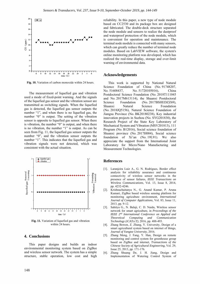
Sensors & Transducers, Vol. 237, Issue 9-10, September-October 2019, pp. 144-149
148
Fig. 10. Variation of carbon monoxide within 24 hours.
The measurement of liquefied gas and vibration used a mode of fixed-point warning. And the signals of the liquefied gas sensor and the vibration sensor are transmitted as switching signals. When the liquefied gas is detected, the liquefied gas sensor outputs the number “1”, and when there is no liquefied gas, the number “0” is output. The setting of the vibration sensor is opposite to liquefied gas sensor. When there is vibration, the number “0” is output, and when there is no vibration, the number “1” is output. As can be seen from Fig. 11, the liquefied gas sensor outputs the number “0”, and the vibration sensor outputs the number “1”. This indicates that the liquefied gas and vibration signals were not detected, which was consistent with the actual situation.
Fig. 11. Variation of liquefied gas and vibration within 24 hours.
4. Conclusions
This paper designs and builds an indoor environmental monitoring system based on ZigBee and wireless sensor network. The system has a simple structure, stable operation, low cost and high
reliability. In this paper, a new type of node module based on CC2530 and its package box are designed and fabricated. The double-deck structure separated the node module and sensors to realize the dustproof and waterproof protection of the node module, which is convenient for operation and maintenance. The terminal node module is connected with many sensors, which can greatly reduce the number of terminal node modules. Based on LabVIEW software, the system's online monitoring platform was developed, which has realized the real-time display, storage and over-limit warning of environmental data. Acknowledgements
This work is supported by National Natural Science Foundation of China (No. 91748207, No. 51608437, No. 51720105016), China Postdoctoral Science Foundation (No. 2018T111045 and No. 2017M613114), the Shaanxi Postdoctoral Science Foundation (No. 2017BSHEDZZ69), Shaanxi Natural Science Foundation (No. 2018JQ5156), Natural Science Foundation of Jiangsu Province (No. BK20180238), Key industrial innovation projects in Suzhou (No. SYG201830), the Research Project of the State Key Laboratory of Mechanical System and Vibration (MSV201813), 111 Program (No. B12016), Social science foundation of Shaanxi province (No. 2017H004), Social science foundation of Xi’an (No. 19L91). We also appreciate the support from the International Joint Laboratory for Micro/Nano Manufacturing and Measurement Technologies. References [1]. Laranjeira Luiz A., G. N. Rodrigues, Border effect
analysis for reliability assurance and continuous connectivity of wireless sensor networks in the presence of sensor failures, IEEE Transactions on Wireless Communications, Vol. 13, Issue 8, 2014, pp. 4232-4246.
[2]. Krishnachaitanya N., G. Anand Kumar, P. Aruna Kumari, ZigBee based wireless sensing platform for monitoring agriculture environment, International Journal of Computer Applications, Vol. 83, Issue 11, 2013, pp. 9-12.
[3]. Sahitya G., N. Balaji, C. D. Naidu, Wireless sensor network for smart agriculture, in Proceedings of the IEEE 2nd International Conference on Applied and Theoretical Computing and Communication Technology (iCATccT), 2016, pp. 488-493.
[4]. Zhang Bowen, Z. Zhang, Y. University, Design of a smart agricultural system based on internet of things, Journal of Yangtze University, 2016.
[5]. Zhang Meng, J. Fang, Y. Han, Design on remote monitoring and control system for greenhouse group based on ZigBee and internet, Transactions of the Chinese Society of Agricultural Engineering, Vol. 29, Issue 25, 2013, pp. 171-176.
[6]. Zhang Shuang De, J. H. Jiang, Design and Implementation of Watering Control System of
Sensors & Transducers, Vol. 237, Issue 9-10, September-October 2019, pp. 144-149
149
Flowers Based on ZigBee, Hubei Agricultural Sciences, 2014.
[7]. Jiang D., Yu L., Wang F., Xie X., Yu Y., Design of the smart home system based on the optimal routing algorithm and ZigBee network, PLos One, Vol. 12, Issue 11, 2017, e0188026.
[8]. Betzler A., Gomez C., Demirkol I., Paradells J., A holistic approach to ZigBee performance enhancement for home automation networks, Sensors, Vol. 14, Issue 8, 2014, pp. 14932-14970.
[9]. Gong Qingchao, G. Li, Y. Pang, Design and implementation of smart home system based on ZigBee technology, Microcomputer Information, 8, 6, 2012, pp. 143-156.
[10]. Zhu Bin, Tang Y., Tan Y., Xia K., Design of ZigBee-based data acquiring and transmission system in industrial control network, Control and Instruments in Chemical Industry, 2010.
[11]. Huang Jiao, H. R. Liu, Design of Intelligent pH Analyzer Based on ZigBee, Control and Instruments in Chemical Industry, 2011.
[12]. Chen Lei, S. Yang, Y. Xi., Based on ZigBee wireless sensor network the monitoring system design for chemical production process toxic and harmful gas, in Proceedings of the International Conference on Computer, Mechatronics, Control and Electronic Engineering, Vol. 4, 2010, pp. 425-428.
[13]. Zhao, Jian Jun, Y. Bai, R. S. Wang, Application of ZigBee technology in chemical water ultrafiltration system, Advanced Materials Research, Vol. 459, 2012, pp. 343-346.
[14]. Ni Yun Feng, J. Liu, Based on ZigBee technology remote health care system design and research, Advanced Materials Research, Vol. 433-440, 2012, pp. 3439-3444.
[15]. Khaliq Kishwer Abdul, Qayyum A., Pannek J., An emergency alert system for elderly/special people using VANET and WBAN, in Proceedings of the IEEE 13th International Conference on Emerging Technologies (ICET), 2017.
[16]. Clarke M., Folter J. D, Verma V., Gokalp H., Interoperable end-to-end remote patient monitoring platform based on IEEE 11073 PHD and ZigBee health care profile, IEEE Transactions on Biomedical Engineering, Vol. 65, Issue 5, 2018.
[17]. Yu T., Dai Z., Li Y., Li Z., Tang L., The research on mine safety auxiliary system of wireless sensor networks, in Proceedings of the IEEE 3rd International Conference on Instrumentation, Measurement, Computer, Communication and Control, 2013, pp. 313-317.
[18]. Castro P., Afonso J. L., Afonso J. A., A Low-Cost ZigBee-Based Wireless Industrial Automation
System, in Proceedings of the Portuguese Conference on Automatic Control, 2017.
[19]. Raza M., Aslam N., Le-Minh H., et al., A Critical Analysis of Research Potential, Challenges and Future Directives in Industrial Wireless Sensor Networks, IEEE Communications Surveys & Tutorials, Vol. 20, Issue 1, 2018, pp. 39-95.
[20]. Hang L., Savkin A. V., Wireless Sensor Network Based Navigation of Micro Flying Robots in the Industrial Internet of Things, IEEE Transactions on Industrial Informatics, Vol. 14, Issue 8, 2018.
[21]. Sahoo P. K., Pattanaik S. R., Wu S. L., A Reliable Data Transmission Model for IEEE 802.15.4e Enabled Wireless Sensor Network under WiFi Interference, Sensors, Vol. 17, Issue 6, 2017, 1320.
[22]. Su F. P., Chen Z. C., Zhou H. F., et al., A distributed monitoring system for photovoltaic arrays based on a two-level wireless sensor network, in Proceedings of the IOP Conference Series: Earth and Environmental Science (EES), Vol. 93, Issue 1, 2017, 012077.
[23]. Barankova I., Mikhailova U., Lukianov G., Automated control system of a factory railway transport based on ZigBee, in Proceedings of the 2nd International Conference on Industrial Engineering, Applications and Manufacturing (ICIEAM), 2017.
[24]. Firdaus, Nugroho E., Sahroni A., ZigBee and WiFi network interface on Wireless Sensor Networks, in Proceedings of the Makassar International Conference on Electrical Engineering & Informatics (MICEEI), 2015.
[25]. Neumeier R., Ostermayer G., Analyzing Coexistence Issues in Wireless Radio Networks: Simulation of Bluetooth Interfered by Multiple WLANs, in Proceedings of the 6th International Workshop on Multiple Access Communications (MACOM 2013), 2013, pp. 599-604.
[26]. Lv Y., Zhang W., Zhang D., et al., An Algorithm for Resisting WiFi Interference in ZigBee, in Proceedings of the 4th International Conference on Information Science & Control Engineering, 2017.
[27]. Blume Peter, The LabVIEW style book, Pearson Education, Inc.,, 2007.
[28]. Zhou Xiaoyi, Electrocardiogram system performance evaluation based on the LabVIEW virtual instruments development platform, in Proceedings of the International Conference in Communications, Signal Processing, and Systems, Springer, Singapore, 2017, pp. 1901-1908.
[29]. Ling-Li H. E., D. O. Imaging, Design of virtual ECG monitor system based on LabVIEW, Chinese Medical Equipment Journal, 2017.
__________________
Published by International Frequency Sensor Association (IFSA) Publishing, S. L., 2019 (http://www.sensorsportal.com).

Sensors & Transducers, Vol. 237, Issue 9-10, September-October 2019, pp. 150-158
150
Sensors & Transducers
Published by IFSA Publishing, S. L., 2019 http://www.sensorsportal.com
Environmental Monitoring System Using Unmanned Aerial Vehicles and WSN
1, 2, * Rosa CAMARILLO, 2 Jorge FLORES, 1 Juana CAMARILLO,
1 Juan RAMIREZ, 1 Eduardo PADILLA and 1 Alfonso VALENCIANA 1 Tecnológico Nacional de Mexico, ITLaguna, Blvd. Revolucion & Cuauhtemoc, S/N,
Center, 27000, Torreón, Coah. Mexico 2 Universidad de Guadalajara, CUCEI, Blvd. Gral. Marcelino García Barragán 1421,
Olímpica, 44430, Guadalajara, Jal., Mexico Tel.: + 52 (871) 7051339
E-mail: [email protected]
Received: 30 August 2019 /Accepted: 27 September 2019 /Published: 30 November 2019 Abstract: In this work, a mobile real-time monitoring system for air quality is proposed. The developed system uses UAV (unmanned aerial vehicles) and WSN (wireless sensor networks), increasing the area of analysis and difficult access. The electronic instrumentation was integrated with an array of sensors, microcontroller, memory and RF modules. The acquired data is stored, processed and transmitted to a computer as a base station through wireless communication, where a developed graphical interface shows the concentrations of polluting gases present in the atmosphere at a minimum height of 10 to 300 m. The weight, size and power consumption of the miniaturized system are 100 g, 50×50×30 cm and 1.5 W respectively. The System was powered by an ion-Li 300 mA/hr battery. The system has the ability to detect important criteria pollutants such as carbon dioxide (CO2), nitrogen dioxide (NO2) and other polluting gases such as Ethanol (C2H5OH), Hydrogen (H2), Ammonia (NH3) and suspended particles PM2.5. Keywords: Air quality, WSN, UAV, Criterial pollutants, Suspended particles PM2.5.
1. Introduction
In recent years, deaths caused by respiratory and cardiovascular diseases have increased by 10 %. In October 2018, the World Health Organization (WHO) stated that 93 % of the world's children breathe polluted air every day. According to this information, 1.8 billion children breathe air so polluted that their health and development are in serious danger. The WHO estimates that 600,000 children died in 2016 from acute respiratory infections caused by air pollution. This increase in atmospherically active gases leads to effects such as soil and water acidification [1]. In 2018, the Torreón city in Mexico,
was ranked fourth in 248, as one of the most contaminated areas of ammonia on the planet [2].
In the absence of a national regulatory for the design and installation of air quality monitoring networks, the networks that currently operate in Mexico have different operational criteria and have strong limitations in terms of availability of financial, human and material resources. For this reason, the design of new networks to measure air quality, as well as the redesign of current networks and the expansion of their coverage, are necessary to improve their operation, by homogenizing the criteria of their establishment, operation and maintenance [3].
http://www.sensorsportal.com/HTML/DIGEST/P_3123.htm

Sensors & Transducers, Vol. 237, Issue 9-10, September-October 2019, pp. 150-158
151
Previously, the measurement of air quality was carried out by non-continuous methods known as "wet chemistry" for gases and high volumes for suspended particles using complex and very expensive stationary equipment [4] to "collect" data. This paradigm is changing, new low-cost and easy-to-use sensors have been developed, providing high resolution and real-time data that can be "accessed" [5]. These attributes provide opportunities to improve a range of existing air pollution monitoring capabilities and provide avenues for new applications. The range of contaminants to be detected by sensors has been increasing. The appearance of new technologies such as UAV, WSN, the internet of things, advances in computing and communications achieves availability and accessibility of data in real time [6].
A key factor in establishing effective air quality monitoring programs is to assign the optimal location for monitoring stations based on five criteria (population, wind direction and spatial proximity to roads, industries and high traffic areas) that were considered the most important for assigning optimal locations for station monitoring [7]. A large number of developments have been reported to measure environmental parameters present in the air as well as the use of technologies. An investigation was made to measure the PM10 fugitive dust emission factors for a range of vehicles types and examined the influence of vehicle and wake characteristics on the strength of emissions from an unpaved road. This study was based on the determination of the vertical mass concentration profile, the speed and direction of the ambient wind, and the time it took to generate a trail of dust when passing through instrumented towers [8]. Another work, determined that the contribution of methane CH4 comes from road traffic and domestic heating, revealing that heating accounts for more than 80 % of the observed CO2 flows. CH4 flows expressed as CO2 equivalents represent approximately 8 % of CO2 emissions, ranging from 16 % in summer to 4 % in winter and, therefore, cannot be neglected when assessing the impact of cities on the greenhouse effect [9]. On the other hand, by 3D computational model predicting extent of gas leakage was made based on the building location using Google Earth. The system was based on the concentration differences at the near wall and far wall, and the velocity field change with the leakage time, to provide reliable data for the city gas safe operation and emergency management [10]. Used on a dedicated Unmanned Aerial Vehicle (UAV) a new instrument was made to map NO2 columns at high spatial resolution allowing to subsample satellite measurements within the extent of a typical ground pixel. The instrument was based on a compact ultra-violet visible spectrometer and a scanner to achieve whiskbroom imaging of the trace gases fields. Including the housing and the electronics [11]. A system online GPRS-Sensors Array was done integrated a Mobile Data-Acquisition Unit (Mobile-DAQ, based a microcontroller, sensors arrays and GPS) and a fixed Internet-Enabled Pollution Monitoring Server (Pollution-Server and Google
Maps to display real-time pollutants), to monitoring air pollutants levels (CO, NO2, and SO2) [12]. The development of these devices allow emissions into the atmosphere to be measured, which would establish permissible limit values that do not present risks to the health of the population and adverse effects to the environment. Other results of an important investigation, shows a study for 10 years where the presence of ammonia affects air quality with consequences on human health, the environment and climate change. Anthropogenic emissions of ammonia dominate the natural ones and originate mainly from agricultural, domestic and industrial activities. The critical ammonia emission points of the world were identified and categorized and quantified using a high resolution map of atmospheric ammonia observed by IASI satellite. In the study, 248 critical points with diameters less than 50 kilometers were located, associating them with specific agricultural and industrial sources. This will lead to better environmental and health impact assessments of atmospheric ammonia and the implementation of appropriate nitrogen management strategies [13]. One of this critical points was located in Torreon, Coahuila, Mexico which is the fourth place of concentration of ammonia in the world. This was the reason the engineering academy started this research project. In this work, a mobile real-time monitoring system for air quality is proposed. The developed system uses UAV unmanned aerial vehicles and WSN wireless sensor networks. The system has the ability to detect important criteria pollutants such as carbon monoxide (CO), nitrogen dioxide (NO2) and other polluting gases such as Ethanol (C2H5OH), Hydrogen (H2), Ammonia (NH3) and Propane (C3H8).
2. Fundamentals
2.1. Standards by Environmental Protection
One of the first standards and measurement systems established for the control of pollutants was born in the United States under the Clean Air Act in 1963, known as NAAQS (National Ambient Air Quality Standards) and established by the Environmental Protection Agency (EPA). This standard establishes concentration levels over a set period of time of the following contaminants:
- Carbon monoxide (CO); - Lead (Pb); - Nitrogen dioxide (NO2); - Ozone (O3); - Suspended particles:
- PM10 (d<10 µm); - PM2.5 (d<2.5 µm).
- Sulfide dioxide (SO2). From NAAQS, the IMECA system (Metropolitan
Air Quality Index) was created in 1982, it is a Mexican standard that uses the bases established by the NAAQS to monitor air quality, at that time focused on

Sensors & Transducers, Vol. 237, Issue 9-10, September-October 2019, pp. 150-158
152
Mexico City and its growing problem of air pollution. The IMECA system provides a standardized way to measure the concentration of pollutants throughout the country, however, it is necessary to take into account a couple of peculiarities about this system. The first is the fact that IMECA was originally conceived as an adaptation with more permissible threshold values than the NAAQS, being the logic for this decision that, if the values established by the American standard were strictly taken, Mexico City would look in a perpetual state of environmental contingency, so it was decided to relax the limits of health risk. The other aspect to consider is that the value indicated by the IMECA scale only gives us the value of the pollutant that presents the greatest risk at that time, being
possible that the concentration of other pollutants can also be found at dangerous levels without being reflected in the value final delivered by the scale [14].
2.2. Different Air Quality Standard Breaking Points
A breaking point is defined as the maximum
acceptable level of a given substance. Any concentration above said measured is considered harmful to public health and the environment. Table 1 indicates the maximum levels allowed by each of the standards.
Table 1. Standard breaking points.
IMECA (Mexican standard) NAAQS (US Standard) *WHO Guidelines
Pollutant Averaging Time Level Averaging
Time Level Averaging Time Level
Ozone(O3) 1 hour 0.11 ppm 8 hours 0.07 ppm 8 hours 0.05 ppm
Carbon Monoxide (CO) 8 hours 11 ppm 8 hours 9 ppm - -
Nitrogen Dioxide (NO2) 1 hour 0.21 ppm 1 hour 0.1 ppm 1 hour 0.1045 ppm
Sulfur Dioxide(SO2) 24 hours 0.13 ppm 1 hour 75 ppb 24 hours 7.51 ppb
PM 10 24 hours 120 µg/m^3 24 hours 150 µg/m^3 24 hours 50 µg/m^3
PM 2.5 24 hours 65 µg/m^3 24 hours 35 µg/m^3 24 hours 25 µg/m^3
*World Health Organization
2.3. Particulate Matter PM2.5
Particle pollution, also called particulate matter or PM, is a mixture of solids and liquid droplets floating in the air. Some particles are released directly from a specific source, while others form in complicated chemical reactions in the atmosphere. They consist of a complex mixture of solid and liquid particles of organic and inorganic substances suspended in the air. The main components of PM are sulfates, nitrates, ammonia, sodium chloride, soot, mineral powders and water. Particles come in a wide range of sizes. Particles less than or equal to 10 micrometers in diameter are so small that they can get into the lungs, potentially causing serious health problems. Ten micrometers is less than the width of a single human hair [15], it´s shown in Fig. 1.
Coarse dust particles (PM10) are 2.5 to 10 micrometers in diameter. Sources include crushing or grinding operations and dust stirred up by vehicles on roads.
Fine particles (PM2.5) are 2.5 micrometers in diameter or smaller, and can only be seen with an electron microscope. Fine particles are produced from all types of combustion, including motor vehicles, power plants, residential wood burning, forest fires, agricultural burning, and some industrial processes.
Fig. 1. Relative size of particulate matter [15].
Generally, air quality monitoring is implemented to determine PM10, although since 2008, WHO has also recommended that PM2.5 be measured in cities because they are the most harmful to health. In addition, in recent years the number of forest fires has increased, further aggravating the environmental situation.
2.4. Ammonia
Ammonia is a chemical substance usually used in refrigeration and fertilizer equipment, which is not

Sensors & Transducers, Vol. 237, Issue 9-10, September-October 2019, pp. 150-158
153
usually considered in the different official standards due to its small presence in natural conditions, being observed in high quantities only in industrial regions where substances are improperly handled or compounds related to this material, or, due to intensive agricultural and livestock activity, which promotes the release of greater than average amounts of fertilizer use [16]. This does not mean that its denomination as a contaminant is not of consideration, since its presence results in the generation of PM 2.5 suspended particles, usually known as aerosols [17]. On the other hand, its presence results in the acidification of soils and waters, which affects the development of vegetation and fauna [18]. Additionally, ammonia has the peculiarity that, when combined with other acidic contaminants such as SO2 and NOx, ammonia (NH3) becomes NH4 +, which has a high diffusion range, extending several hundred kilometers from its point of origin (between 100 and 1000 km) [19]. The principal of ammonia concentrations shown in Fig. 2.
Fig. 2. Ammonia concentration map [13].
Ammonia can be a provider of an abundant amount of condensation nuclei in the form of ammonium nitrate (and ammonium sulphate) which, under favourable meteorological conditions, attract hygroscopic water, leading to rapid increase in the PM2.5 mass fraction [17]. The maximum limit allowed is 25 ppm.
2.5. Measurement Sensors For the acquisition of data on the presence of gases
in the air, the sensor by means of a resistance it is possible to obtain a dimensionless relation of resistances that determines the ppm of each element. The concentration of contaminating gases was determined by the relationship:
RsxRo
= , (1)
where x is the gas to be measured in ppm, Rs is the resistance of the sensor in Ω, Ro the adjustment resistance. Ro = 22 kΩ for NOx and Ro = 45 kΩ for residual gases [20].
For the acquisition of data of suspended particles, an optical sensor measure particles over 1 µm and 2.5 µm in size. In order to get a reading, air passes through the bottom intake while the heating element (a resistor) heats the air, which forces particles to rise up and block the infrared light emitted by the IR LED which in turn provides a photodiode a signal in order to detect the variation in light levels which correlates to the presence of particles in the air. In optic system is necessary to provide a stable supply in this case 5 V, and sample time of at least 30 seconds, during which the microcontroller must measure the sum of all LOW signal periods in order to determine the concentration of particles in the air.
For the purposes of this project, was used calibrating equation in order to measure the concentration of particles in µg/m³ [21].
22.5 0.1809 ( ) 3.8987 ( ),PM ratio ratio= × + × (2)
where ratio is the amount of time the sensor signal was LOW. In order to get a better reading, an average over a longer period of time is advised in order to filter out any noisy readings.
3. Experimental The mobile system for air quality monitoring uses
emerging technologies such as UAV and WSN. The electronic instrumentation was integrated with high-range microdevices. A small wireless network of 2 nodes was implemented as an application example. An electronic control was implemented for the acquisition, storage, processing and transmission of data. It was integrated a Robust MEMS smart sensor node MiCS 4514 (SGX Sensortech, Switzerland) with capacity to detect up to 6 pollutant gases and a module optic sensor of suspended particles DSM 501A (Samyoung S&C, Korea). The electronic control can communicate up to a distance of 750 m. between nodes and towards the base station by a PC. A storage system to protect acquired data was integrated, it shown in Fig. 3.
The electronic control was mounted in each UAV, making the mobile monitoring system an autonomous device. A small UAV (drone) Spark dji was used (dgi, USA). For the support of electronic control, a structure in PLA material was manufactured using a desktop 3D printer (FlashForge Creator Pro, China) as shown in Fig. 4.
The acquired data is transmitted through RF modules to a computer, where a graphical interface processes and shows in real time the concentration of contaminating gases in ppm. The graphical interface was programmed in LabVIEW and it is show in Fig. 5.
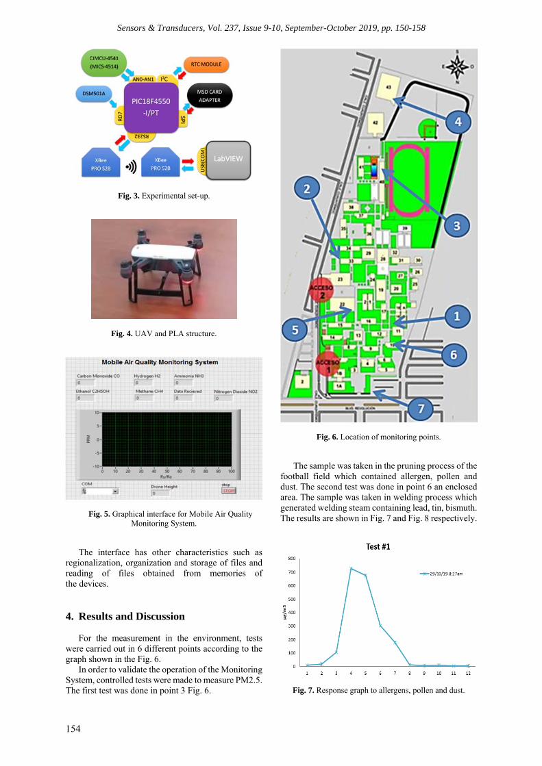
Sensors & Transducers, Vol. 237, Issue 9-10, September-October 2019, pp. 150-158
154
Fig. 3. Experimental set-up.
Fig. 4. UAV and PLA structure.
Fig. 5. Graphical interface for Mobile Air Quality Monitoring System.
The interface has other characteristics such as regionalization, organization and storage of files and reading of files obtained from memories of the devices. 4. Results and Discussion
For the measurement in the environment, tests were carried out in 6 different points according to the graph shown in the Fig. 6.
In order to validate the operation of the Monitoring System, controlled tests were made to measure PM2.5. The first test was done in point 3 Fig. 6.
Fig. 6. Location of monitoring points.
The sample was taken in the pruning process of the football field which contained allergen, pollen and dust. The second test was done in point 6 an enclosed area. The sample was taken in welding process which generated welding steam containing lead, tin, bismuth. The results are shown in Fig. 7 and Fig. 8 respectively.
Fig. 7. Response graph to allergens, pollen and dust.
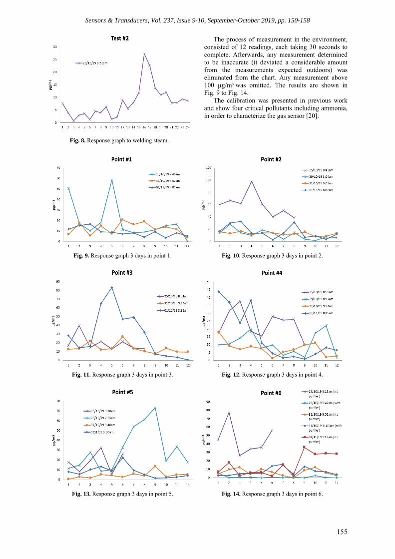
Sensors & Transducers, Vol. 237, Issue 9-10, September-October 2019, pp. 150-158
155
Fig. 8. Response graph to welding steam.
The process of measurement in the environment, consisted of 12 readings, each taking 30 seconds to complete. Afterwards, any measurement determined to be inaccurate (it deviated a considerable amount from the measurements expected outdoors) was eliminated from the chart. Any measurement above 100 µg/m³ was omitted. The results are shown in Fig. 9 to Fig. 14.
The calibration was presented in previous work and show four critical pollutants including ammonia, in order to characterize the gas sensor [20].
Fig. 9. Response graph 3 days in point 1.
Fig. 10. Response graph 3 days in point 2.
Fig. 11. Response graph 3 days in point 3.
Fig. 12. Response graph 3 days in point 4.
Fig. 13. Response graph 3 days in point 5. Fig. 14. Response graph 3 days in point 6.

Sensors & Transducers, Vol. 237, Issue 9-10, September-October 2019, pp. 150-158
156
Other measuring were made to evaluate the presence of gases mainly CO2, NO2 and NH3 in outdoor environment. The response of air quality monitoring system are show in Fig. 15 to Fig. 20.
Environmental tests of air quality were performed in Torreon, Coah., Mexico. Figs. 21-22 show the aerial view of city. The system was probed to measure traffic pollution at peak hours and industrial operations at 100 % (13:00 hrs) at a flight height of 15 to 30 meters.
Fig. 15. Response graph in point 3.
Fig. 16. Response graph in point 6.
Fig. 17. Response graph in point 7.
Fig. 18. Response graph in point 3.
Fig. 19. Response graph in point 6. Fig. 20. Response graph in point 7.
According to the SMN (national meteorological
system) of the CONAGUA, there are four monitoring stations in Torreon, 5006, 5026, 5029 and 5040, of which only one operates and located in the La Flor dam (5029). In addition, as critical data, the records history of environmental measurements are not updated, they only report to 2010.
Due to the above, until the dates reported in this work were not validated with official records. It is important to have updated, truthful and timely information in real time on air pollution rates, as it has been shown that Torreon is among the specific emitters of atmospheric ammonia. The work presented here, is a step to the initiative for the conservation of

Sensors & Transducers, Vol. 237, Issue 9-10, September-October 2019, pp. 150-158
157
the environment and generate information for the prevention of diseases caused by poor air quality.
Fig. 21. Torreon aerial view early in the morning.
Fig. 22. Torreon midday aerial view.
Children, people over 65, pregnant women and people with heart or lung diseases (including asthma) are more sensitive to the effects of breathing these particles. Symptoms may include wheezing - acute wheezing through the respiratory ducts - chest tightness and shortness of breath.
In addition, high levels of PM 2.5 also cause irritation to the eyes, nose and throat; cough, chest tightness and trouble breathing; reduced lung function; asthma attacks; heart attacks and premature death in people with heart and lung diseases.
5. Conclusions
A wireless distributed mobile air pollution monitoring system was designed, implemented and tested using the UAV and WSN. The system measured concentration of pollutant gases such as CO, NO2, NH3 and PM2.5. The pollution data from various mobile sensor arrays is transmitted to a central server in PC and storing data in a micro-sd memorycard. The data shows the pollutant levels and should be considered by the local air quality regulatory.
The system is based in MICS-4514 sensor and it is focused on the detection of residual gases (RED) and nitrogen gases (NOX). It is mainly dedicated to CO and NO2, but it is also capable of detecting ammonia, propagation, ethanol, hydrogen and H2S values with certain limits.
On the other hand, the System also has the ability to detect PM2.5, obtaining a high sensitivity of response both in laboratory experimentation and environmental tests.
In this short sampling it was found that if there is NO2 in the air, the presence of NH3 and the increase in PM2.5 are also shown.
A lot of work is required to complete a robust system. We recommend more tests to be done for a solid conclusion about the pollution of ammonia.
Acknowledgements
The authors thank to M.C. Juan Antonio Ramirez Bruno, for the partial financing of this project and Cristian Alberto Serrano López, for the design and manufacture of the support structures by means of FDM additive manufacturing used in this work. References [1]. Tecnologia Ambiental, «Tecnologia Ambiental»,
15 02 2017. [Online]. https://tecnologiaambiental.mx/ 2017/03/09/aire-puro/. [Último acceso: 15 02 2019].
[2]. M. Vann Dame, et al., Industrial and agricultural ammonia ponit sources exposed, Nature. International Journal of Science, Vol. 564, 2018, pp. 99-103.
[3]. SINAICA-SEMARNAP-INECC, Manual Redes Estaciones y Equipos de Medicion de la Caliad del Aire, Instituto Nacional de Ecologia, Ciudad de Mexico, 2016.
[4]. J. C. Chow, Measurement methods to determine compliance with ambient air quality standards for suspended particles, J Air Waste Manage Assoc., Vol. 45, Issue 5, 1995, pp. 320-382.
[5]. E. G. Snyder, et al., The changing paradigm of air pollution monitoring, Environmental Sci. & Technol., Vol. 47, Issue 20, 2019, pp. 11369-11377.
[6]. R. M. White, et al., Sensors and Apps for community-based: Atmospheric monitoring, Air Waste Manage. Ass. Magazine for Envronmental Manager, Vol. 5, 2012, pp. 36-40.
[7]. Mohammad M. Alsahli, Meshari Al-Harbi, Allocating optimum sites for air quality monitoring stations using, Urban Climate, Vol. 24, 2018, pp. 875–886.
[8]. J. A. Gillies, V. Etyemezian, H. Kuhns, D. Nikolic, D. A. Gillette, Effect of vehicle characteristics on unpaved, Atmospheric Environment, Vol. 39, Issue 13, 2005, pp. 2341-2347.
[9]. B. Gioli, P. Toscano, E. Lugato, A. Matese, F. Miglietta, A. Zaldei, F. P. Vaccari, Methane and carbon dioxide fluxes and source partitioning in urban areas: The case study of Florence, Italy, Environmental Pollution, Vol. 164, 2012, pp. 125-131.

Sensors & Transducers, Vol. 237, Issue 9-10, September-October 2019, pp. 150-158
158
[10]. Liu Fei, Chu Yan-yan, Liang Dong, Simulation of Urban Gas Leakage Based on Google Earth, Procedia Engineering, Vol. 52, 2013, pp. 220-224.
[11]. Merlaud Alexis, et al., Small Whiskbroom Imager for atmospherIc compositioN monitorinG (SWING) from an Unmanned Aerial Vehicle (UAV), Atmospheric Measurement Techniques, Vol. 11, Issue 1, 2018, pp. 551-567.
[12]. A. R. Al-Ali, Imran Zualkernan, Fadi Aloul, A Mobile GPRS-Sensors Array for Air Pollution Monitoring, IEEE Sensrs Journal, Vol. 10, Issue 10, 2010, pp. 1666-1671.
[13]. Martin Van Damme, Lieven Clarisse, Simon Whitburn, Juliette Hadji-Lazaro, Daniel Hurtmans, Cathy Clerbaux & Pierre-François Coheur, Industrial and agricultural ammonia point sources exposed, Nature, Vol. 564, 2018, pp. 99-103.
[14]. E. Escurra, «¿Qué mide el IMECA?,» Revista Ciencias, No. 22, 1991, pp. 41-43.
[15]. U. S. E. P. Agency, Airnow, 17 01 2017. [Online]. https://cfpub.epa.gov/airnow/index.cfm?action=aqibasics.particle. [Último acceso: 03 11 2019].
[16]. Scottish Environment Protection Agency (SEPA), 26 10 2017. [Online]. Available:
http://apps.sepa.org.uk/spripa/Pages/SubstanceInformation.aspx?pid=1. [Last visit: 02 10 2019].
[17]. Mensink C., Deutsch F., On the Role of Ammonia in the Formation of PM2.5., de Air Pollution Modeling and Its Application XIX., Springer, Switzerland, Dordrecht, 2008, pp. 548-556.
[18]. Guthrie Susan, Giles Sarah, Dunkerley Fay, Tabaqchali Hadeel, Harshfield Amelia, Loppolo Becky, Manville Catriona, The impact of ammonia emissions from agriculture on biodiversity, Cambridge UK: Royal Society, 2018.
[19]. Willem A. H. Asman, Mark A. Sutton, Jan K. Schjørring, Ammonia: emission, atmospheric transport, New Phytol, Vol. 139, 1998, pp. 27-48.
[20]. Camarillo R. M., Flores J., et al., Mobile air quality monitoring system using Unmanned Aerial Vehicles & Wireless Sensors Networks, in Proceedings of the 5th International Conference on Sensors Engineering and Electronics Instrumentation Advances (SEIA'19), Tenerife (Canary Islands), 25-27 September 2019, pp.148-152.
[21]. Dust Sensor Module P/N: DSM501 Data Sheet, Samyoung S&C, Korea, 2014.
__________________
Published by International Frequency Sensor Association (IFSA) Publishing, S. L., 2019 (http://www.sensorsportal.com).

Sensors & Transducers, Vol. 237, Issue 9-10, September-October 2019, pp. 159-164
159
Sensors & Transducers
Published by IFSA Publishing, S. L., 2019 http://www.sensorsportal.com
New Approach to Optimization of Crop Production and Environment Protection
1 Olga CHAMBERS, 1, * Janez TRONTELJ, 2 Jurij TASIC
and 1 Janez TRONTELJ jr.
1 University of Ljubljana, Faculty of Electrical Engineering, Laboratory for Microelectronics, Trzaska 25, 1000 Ljubljana, Slovenia
2 Innovation technologies d.o.o., 8290 Sevnica, Slovenia E-mail: [email protected]
Received: 30 August 2019 /Accepted: 27 September 2019 /Published: 30 November 2019 Abstract: It is well known that soil preparation plays a key role for optimization of the crop. It is less known that some fertilizer reach a plant root system below 20 cm after two or more years if applied at the soil surface. Also a large portion of the fertilizer never reaches the plant roots. As a consequence the large amount of the fertilizer is lost due to over dosage is used. In addition the excess fertilizer merges into undesired environment like ground water, plant leaves etc. and is spread by flies, bees and other bugs and finally end up in animal nutrients or human food. The solution to the problem is to provide the fertilizer under the ground level close to the plant root system, with the right composition of the nutrients and with the right quantity. In the paper we are presenting an agricultural machine capable to penetrate underground about 30 cm with vibrating tools and with the automatic dosage of different required fertilizers. The remaining problem is how to analyze the soil on the fly to determine which nutrients are missing and how much is needed to fulfill the optimal calculated fertilization plan. In the paper the soil characterization methods are briefly discussed and the results of the proposed soil electrical impedance frequency specter are presented and discussed [1]. Keywords: Soil classification, Soil impedance spectroscopy, Real-time soil sensor. 1. Introduction
Soil analysis is an essential problem that plays an important role in a nowadays agriculture. Literature indicates a common use of optical and impedance methods for soil quantitative and qualitative analysis, that may be used to design low-cost portable sensors for real-time application, i.e. on-the go soil sensors [2]. Therefore, a number of strategies with different degrees of success have been proposed for the environmental effects and soil properties prediction in a field. This paper is addressing the problem of the soil pre-processing prior to the measurements, as it can be
critical due to a large number of unknown parameters when using the soil impedance spectroscopy, being the most promising soil classification method on the spot.
The goal is to perform the spectral analysis of the soil sample within less than few seconds time that includes the soil sample preparation, measurement and classification.
Among the soil classification principles the chemical analysis is the most accurate, but it requires a long delay time to obtain the results from the certified laboratory, and is therefore unsuitable for the application on the field, however if offers valuable reference results.
http://www.sensorsportal.com/HTML/DIGEST/P_3124.htm

Sensors & Transducers, Vol. 237, Issue 9-10, September-October 2019, pp. 159-164
160
Other methods addressed in the paper are Visual and Near InfaRared (VIS, NIR) optical spectroscopy, optical analysis of dried droplets of the liquid with a mixture of soil and water containing the soil. Both methods allow the soil classification but proved to be slower and less suitable for on the fly classification.
The soil impedance spectra do not show directly the contents of the nutrients, intelligent algorithms need to be applied to recognize the specific nutrient and its quantity.
The soil classificatory device will be assembled into agricultural tool called vibrational sub- soiler (Fig. 1).
Fig. 1. Vibrational sub-soiler INO Brezice.
The attachment to regular tractor, the sub-soiler is shown in Fig. 2. It has an innovative pneumatic system to deliver the fertilizer mixture under the soil surface.
Fig. 2. Detail of vibrational sub-soiler INO Brezice.
Vibrational 2-row sub-soiler with pneumatic fertilizer device is intended for subsoiling the ground and for underground fertilizing in vineyards and orchards. It performs the following tasks:
- Subsoiling the ground close to the root structure.
- Increasing the aeration, permitting the filtering of the water from the surface down through the ground profile and allowing the moisture to be stored for the use during dry periods.
- Fertilizing close to the root structure under the pressure 1 bar. In this way fertilizer (K, P, Mg) moves freely to the roots.
When fertilizing over the ground, only a low quantity is infiltrated into the ground and by the time fertilizer loses its nature.
2. Soil Classification Methods
2.1. Chemical
Chemical analysis is most commonly used method to classify the soil quality in terms of its fertility and its content of the fertilizers. Based on this analysis, the fertilization plan is created and applied. This method is most accurate and reliable, but it needs to be performed in the certificated laboratory. This means a long delay to receive the result and is not suitable for the immediate application on the field.
2.2 Optical
Visual (VIS) and Near Infra-Red NIR spectroscopy is a promising technology. An example of soil spectra is shown in Fig. 3 for different soil samples with different types of nutrition added. The spectra do offer a possibility to classify the soil, however the procedure is too slow and too sensitive for on the field and on the fly operation.
Fig. 3. Soils spectra of various soil types.
2.3. Droplets Analysis
Soil solution droplets analysis is one other possible way to classify the soil. An example of soil droplets of different soil samples with different concentration of fertilizers is shown in Fig. 4.
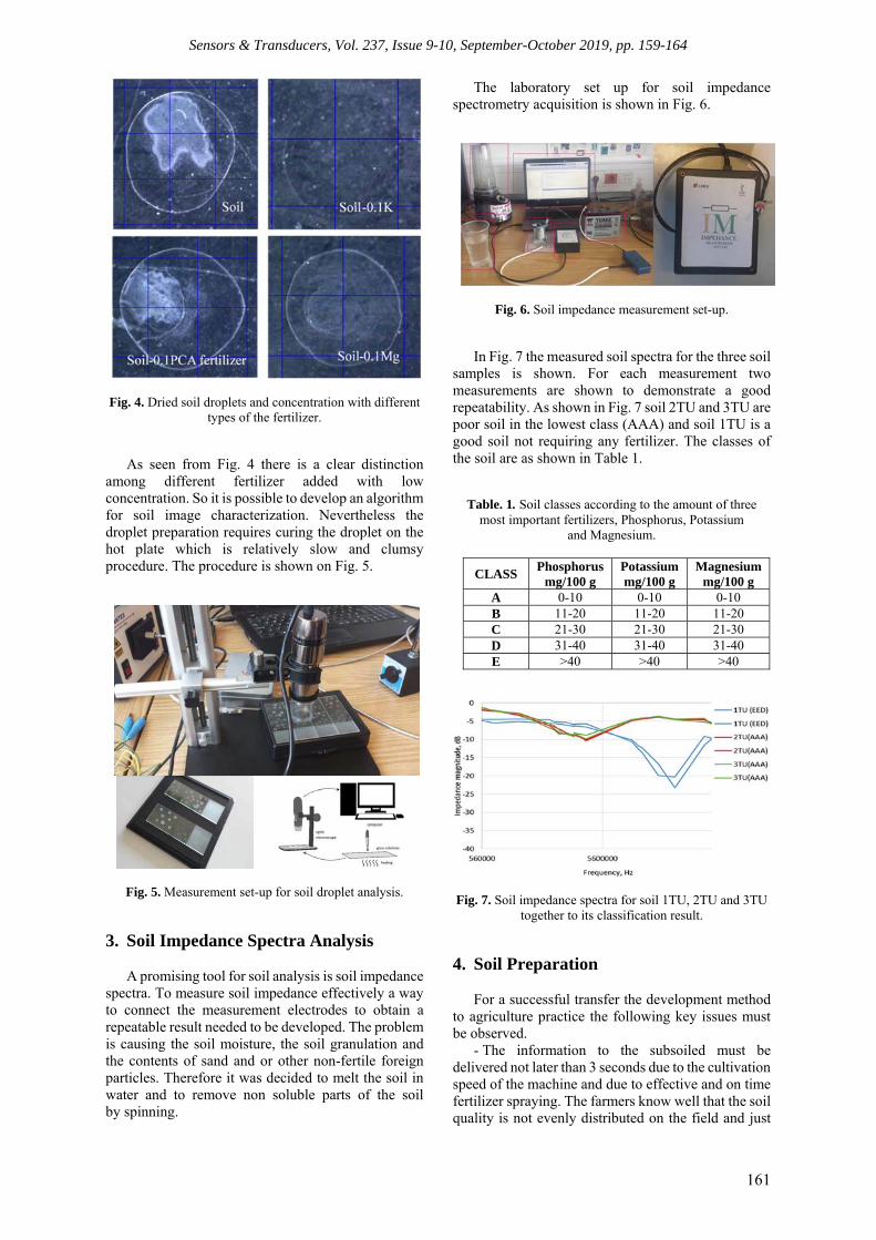
Sensors & Transducers, Vol. 237, Issue 9-10, September-October 2019, pp. 159-164
161
Fig. 4. Dried soil droplets and concentration with different types of the fertilizer.
As seen from Fig. 4 there is a clear distinction among different fertilizer added with low concentration. So it is possible to develop an algorithm for soil image characterization. Nevertheless the droplet preparation requires curing the droplet on the hot plate which is relatively slow and clumsy procedure. The procedure is shown on Fig. 5.
Fig. 5. Measurement set-up for soil droplet analysis.
3. Soil Impedance Spectra Analysis
A promising tool for soil analysis is soil impedance spectra. To measure soil impedance effectively a way to connect the measurement electrodes to obtain a repeatable result needed to be developed. The problem is causing the soil moisture, the soil granulation and the contents of sand and or other non-fertile foreign particles. Therefore it was decided to melt the soil in water and to remove non soluble parts of the soil by spinning.
The laboratory set up for soil impedance spectrometry acquisition is shown in Fig. 6.
Fig. 6. Soil impedance measurement set-up.
In Fig. 7 the measured soil spectra for the three soil samples is shown. For each measurement two measurements are shown to demonstrate a good repeatability. As shown in Fig. 7 soil 2TU and 3TU are poor soil in the lowest class (AAA) and soil 1TU is a good soil not requiring any fertilizer. The classes of the soil are as shown in Table 1.
Table. 1. Soil classes according to the amount of three most important fertilizers, Phosphorus, Potassium
and Magnesium.
CLASS Phosphorus mg/100 g
Potassium mg/100 g
Magnesium mg/100 g
A 0-10 0-10 0-10 B 11-20 11-20 11-20 C 21-30 21-30 21-30 D 31-40 31-40 31-40 E ˃40 ˃40 ˃40
Fig. 7. Soil impedance spectra for soil 1TU, 2TU and 3TU together to its classification result.
4. Soil Preparation
For a successful transfer the development method to agriculture practice the following key issues must be observed.
- The information to the subsoiled must be delivered not later than 3 seconds due to the cultivation speed of the machine and due to effective and on time fertilizer spraying. The farmers know well that the soil quality is not evenly distributed on the field and just
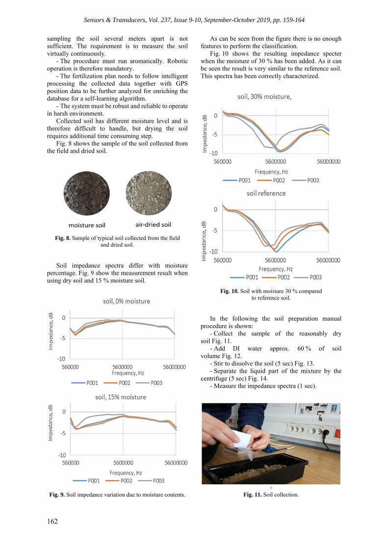
Sensors & Transducers, Vol. 237, Issue 9-10, September-October 2019, pp. 159-164
162
sampling the soil several meters apart is not sufficient. The requirement is to measure the soil virtually continuously.
- The procedure must run aromatically. Robotic operation is therefore mandatory.
- The fertilization plan needs to follow intelligent processing the collected data together with GPS position data to be further analyzed for enriching the database for a self-learning algorithm.
- The system must be robust and reliable to operate in harsh environment.
Collected soil has different moisture level and is therefore difficult to handle, but drying the soil requires additional time consuming step.
Fig. 8 shows the sample of the soil collected from the field and dried soil.
Fig. 8. Sample of typical soil collected from the field and dried soil.
Soil impedance spectra differ with moisture percentage. Fig. 9 show the measurement result when using dry soil and 15 % moisture soil.
Fig. 9. Soil impedance variation due to moisture contents.
As can be seen from the figure there is no enough features to perform the classification.
Fig. 10 shows the resulting impedance specter when the moisture of 30 % has been added. As it can be seen the result is very similar to the reference soil. This spectra has been correctly characterized.
Fig. 10. Soil with moisture 30 % compared to reference soil.
In the following the soil preparation manual procedure is shown:
- Collect the sample of the reasonably dry soil Fig. 11.
- Add DI water approx. 60 % of soil volume Fig. 12.
- Stir to dissolve the soil (5 sec) Fig. 13. - Separate the liquid part of the mixture by the
centrifuge (5 sec) Fig. 14. - Measure the impedance spectra (1 sec).
+ Fig. 11. Soil collection.
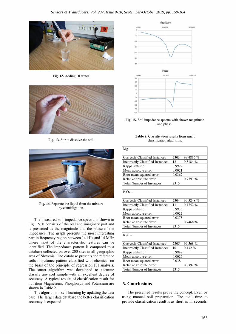
Sensors & Transducers, Vol. 237, Issue 9-10, September-October 2019, pp. 159-164
163
Fig. 12. Adding DI water.
Fig. 13. Stir to dissolve the soil.
Fig. 14. Separate the liquid from the mixture by centrifugation.
The measured soil impedance spectra is shown in Fig. 15. It consists of the real and imaginary part and is presented as the magnitude and the phase of the impedance. The graph presents the most interesting part in frequency region between 14 kHz and 14 MHz where most of the characteristic features can be identified. The impedance pattern is compared to a database collected on over 200 sites in all geographic area of Slovenia. The database presents the reference soils impedance pattern classified with chemical on the basis of the principle of regression [3] analysis. The smart algorithm was developed to accurate classify any soil sample with an excellent degree of accuracy. A typical results of classification result for nutrition Magnesium, Phosphorus and Potassium are shown in Table 2.
The algorithm is self-learning by updating the data base. The larger data database the better classification accuracy is expected.
Fig. 15. Soil impedance spectra with shown magnitude and phase.
Table 2. Classification results from smart classification algorithm.
Mg – Correctly Classified Instances 2303 99.4816 % Incorrectly Classified Instances 12 0.5184 % Kappa statistic 0.9922 Mean absolute error 0.0021 Root mean squared error 0.0367 Relative absolute error 0.7793 % Total Number of Instances 2315 P2O5 – Correctly Classified Instances 2304 99.5248 % Incorrectly Classified Instances 11 0.4752 % Kappa statistic 0.9936 Mean absolute error 0.0022 Root mean squared error 0.0375 Relative absolute error 0.7468 % Total Number of Instances 2315 K2O – Correctly Classified Instances 2305 99.568 % Incorrectly Classified Instances 10 0.432 % Kappa statistic 0.9942 Mean absolute error 0.0025 Root mean squared error 0.038 Relative absolute error 0.8392 % Total Number of Instances 2315
5. Conclusions
The presented results prove the concept. Even by using manual soil preparation. The total time to provide classification result is as short as 11 seconds.

Sensors & Transducers, Vol. 237, Issue 9-10, September-October 2019, pp. 159-164
164
It is reasonably to believe that the robot can shorten the time to the requested 3 seconds. The solution presented is affordable and can be multiplied to provide. A parallel operation and therefore scan the soil with dense grid tom fertilize the soil more evenly and to expect an even crop over all treated area. The cost of fertilizer is dramatically reduced and the negative impact of farming to environment is minimized.
Acknowledgements
The authors would like to thank the Slovenian Research Agency to cofound the research.
References [1]. Chambers Olga, Trontelj Janez, Tasič Jurij F., On the
fly soil classification using impedance spectroscopy, in Proceedings of the 5th International Conference on Sensors and Electronic Instrumentation Advances (SEIA'2019), Adeje, Tenerife (Canary Islands), Spain, 25-27 September 2019, pp. 61-62.
[2]. Chambers Olga, Sešek Aleksander, Ražman Rok, Tasič Jurij F., Trontelj Janez, Fertilizer characterization using optical and electrical impedance methods, Computers and Electronics in Agriculture, Vol. 155, December 2018, pp. 69-75.
[3]. J. Friedman, T. Hastie, R. Tibshirani, Additive logistic regression: a statistical view of boosting, The Annals of Statistics, Vol. 28, Issue 2, 2000, pp. 337–407.
__________________
Published by International Frequency Sensor Association (IFSA) Publishing, S. L., 2019 (http://www.sensorsportal.com).
Sensors & Transducers, Vol. 237, Issue 9-10, September-October 2019, pp. 165-170
165
Sensors & Transducers
Published by IFSA Publishing, S. L., 2019 http://www.sensorsportal.com
Evaluation Results of Testing of the Measuring
Instruments Software
1, * O. VELYCHKO, 2 O. HRABOVSKYI and 2 T. GORDIYENKO 1 State Enterprise ‘All-Ukrainian State Scientific and Production Centre for Standardization,
Metrology, Certification and Protection of Consumer’, (SE ‘Ukrmetrteststandard’), 4 Metrologichna str., Kyiv, 03143, Ukraine
2 Odesa State Academy of Technical Regulation and Quality, 15 Kovalska str., Odesa, 65020, Ukraine 1 Tel.: + 38 050 464 00 24, + 38 097 177 57 43, fax: + 38 044 526 03 35
* E-mail: [email protected]
Received: 30 August 2019 /Accepted: 27 September 2019 /Published: 30 November 2019 Abstract: The developed special methodology of evaluation results of the testing of measuring instruments software (MI SW) with taking into account all essential requirements of OIML document and WELMEC guidelines was presented. This methodology contains the methodology for testing of MI SW on the following generalized indicators. The developed methodology for the testing of some varieties of MI SW with built-in computer was used. The obtained results showed the possibility of applying the Rasch model for the analysis of the scale for evaluating of results of the testing MI SW. Keywords: Software, Measuring instruments, Testing, Evaluation, Rasch model. 1. Introduction
Specialized software (SW) for measuring instruments (MIs) is subject to testing for conformity assessment of MI. The testing of MI SW is devoted to the documents of the International Organization of Legal Metrology (OIML) [1] and the guidelines of the European Organization for Cooperation in Legal Metrology (WELMEC) [2-3].
Since 2005 in Ukraine, national metrology institutes have been carry out of work on the testing of MI SW [4-5]. In 2013, the national standard DSTU 7363 [6] has been developed, which sets the general technical requirements for MI SW. This standard only partly meets the requirements of international and regional documents and guidelines. On the basis of DSTU 7363 developed special methodical recommendations for the testing of SW MI.
In [7], a comparative analysis of the general requirements in the documents and guidelines of the international and regional organizations of legal metrology OIML and WELMEC concerning the testing of MI SW was conducted. In this work a universal algorithm for testing of MI SW is proposed.
In [8], an analysis of the normative framework for testing of MI SW at the national level was conducted to determine its suitability for carrying out conformity assessment. It has been established that DSTU 7363 [6] contains only general SW protection requirements and does not define the SW testing methodology.
National metrology institutes and conformity assessment bodies are interested in the existence of effective testing methodology for MI SW, risk assessment and application-related threats. Actual issues are the development of national SW testing
http://www.sensorsportal.com/HTML/DIGEST/P_3125.htm

Sensors & Transducers, Vol. 237, Issue 9-10, September-October 2019, pp. 165-170
166
procedures for MI SW taking into account all essential requirements of OIML document [1] and WELMEC guidelines [2-3]. At the same time, it is important to conduct an analysis of the practical testing of national SW testing procedures for MI SW with purpose of its suitability for use [9].
2. The Main Content of the Research
On the basis of the conducted analysis, a special SW testing methodology of MI SW was developed taking into account all essential requirements of OIML document [1] and WELMEC guidelines [2-3]. This methodology contains the methodology for testing of MI SW on the following generalized quality indicators:
КP is indicator of software characteristics with built-in computer;
КU is indicator of software characteristics with a universal computer;
КL is indicator of checking storage devices; КT is indicator of verification of data
transmission devices; КS is indicator of checking of reading; КD is indicator of checking of SW sharing levels; КI is a special indicator of SW testing for a specific
MI. For each of these generalized quality indicators
(main requirements), the relevant partial indicators (specific requirements) are determined and the expressions are set for the numerical value of the indicator.
The numerical value for each generalized quality indicator is determined by the expression:
1
,M
Kk i i
i
K K w M=
= (1)
where M is the total number of estimated partial indicators for a certain generalized indicator; Кi is the partial indicators for a certain generalized indicator;
Kiw is the weighting coefficient of the corresponding
partial indicator. In [10] a comparative analysis of the results of
conformity assessment of MI SW was carried out. The generalized and particular quality indicators were selected for assessing the quality of MI software and expressions to obtain the numerical value of each partial indicator for each generalized indicator were developed. For comparative evaluation, the Analytic Hierarchy Process (AHP) was used, since it allows comparing and quantifying alternative solutions [11-12]. For pairwise comparison of all quantitative and qualitative indicators with the presentation of the equation in a quantitative form, the Saati scale was used.
In accordance with requirements of the WELMEC guidelines for testing MI SW at the beginning of the evaluation, it is necessary to determine to which basic configuration this SW is related to: with a built-in
computer P or with a universal computer U. In the further, it is necessary to use the full set of requirements (quality indicators) that relate to the corresponding basic configuration. The KP and KU quality indicators are important by default.
In the developed methodology, all of the above indicators, its partial indicators and its numerical scales are used as in [9]. КP has 7 partial indicators; КU – 9; КL – 8; КT – 8; КS – 3; КD – 4; КI – 6. In general, the total indicator Кtot for MI SW can be estimated as a simple sum of all generalized indicators. The higher a numerical value for MI SW, the more preferable it is MI SW.
The developed methodology for the testing of six varieties of MI SW with built-in computer Р (meters of electric and thermal energy, gas-dispensing columns, gas chromatograph) was used. The testing results in the evaluation of compliance of SW1–SW6 by methodology are shown in Table 1 and Fig. 1.
The analysis of the obtained results shows the advantage of MI SW in the following sequence: SW1 > SW5 > SW2 > SW6 > SW3 > SW4. At the same time, the КS and КD indicators a have the same values for all MI SW. It is determined that those indicators are practically inapplicable and can be neglected.
Table 1. Results of testing SW for generalized indicators.
КP КL КT КS КD КI Кtot
SW1 9 8 5 1 1 7 31 SW5 9 8 4 1 1 7 30 SW2 9 7 3 1 1 7 28 SW6 9 7 4 1 1 6 28 SW3 9 6 4 1 1 6 27 SW4 9 8 5 1 1 3 27
Fig. 1. Results of testing SW for generalized indicators.
In recent decades, Rasch mathematical model [13–17] is widely used to create new or to view existing scales. This model ensures that valid results are obtained through the use of statistics of adequacy, diagnostic information; presents test parameters on a single common linear scale, which helps in the criterion-oriented interpretation of the data.
0123456789
10
КP KL KT KS KD KI
SW1 SW2 SW3 SW4 SW5 SW6
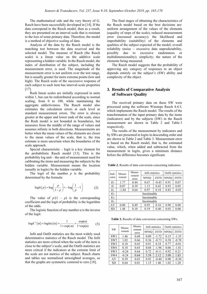
Sensors & Transducers, Vol. 237, Issue 9-10, September-October 2019, pp. 165-170
167
The mathematical side and the very theory of G. Rasch have been successfully developed in [14]. If the data correspond to the Rasch model, then as a result, they are presented on an interval scale that is resistant to the loss of some primary data. Therefore, the model is a method of objective scaling of data.
Analysis of the data by the Rasсh model is the matching test between the data received and the selected model. The measure of Rasсh (the Rasch scale) is a linear value on the additive scale representing a hidden variable. In the Rasch model, the index of distribution of the subject, including the measurement error, is used. The magnitude of the measurement error is not uniform over the test range, but is usually greater for more extreme points (low and high). The Rasch scale of the successive response of each subject to each item has interval-scale properties [17].
Rush linear scales are initially expressed in units within 1, but can be redistributed according to normal scaling, from 0 to 100, while maintaining the aggregate addictiveness. The Rusch model also estimates the calculation errors at each level as standard measurement errors. The error is always greater at the upper and lower ends of the scale, since the Rush model is not bounded in boundaries, but measures from the middle of the range of values and assumes infinity in both directions. Measurements are better when the mean values of the elements are closer to the mean values of the scale, that is, the true estimate is more uncertain when the boundaries of the scale approach.
Special characteristic – logit is a key element for the probabilistic Rasch model [13]. This is the probability log unit – the unit of measurement used for calibrating the items and measuring the subjects by the hidden variable. Measurement means the location (usually in logits) by the hidden variable.
The logit of the number p is the probability determined by the formula:
( ) 1logit log log 1
1
pp
p p
= = − − −
(2)
The value of p/(1 – p) is the corresponding coefficient and the logit of probability is the logarithm of the odds.
The logistic function of any number α is the inverse of the logit:
( ) ( )1 1 exp(α)logit logitic
1 exp(-α) 1+exp(α)− α = α = =
+ (3)
Infit and Outfit statistics are the most widely used determinative statistics of the Rasch model. The Infit statistics are more critical when the scale of the item is close to the subject’s scale, and the Outfit statistics are more critical if the indicators at the extreme limit of the scale are not metrics of the subject. Rasch charts and tables use normalized unweighted averages, so that the graphs are symmetric centered to zero [18].
The final stages of obtaining the characteristics of the Rusch model based on the best decisions are: uniform arrangement of the values of the elements (equality of steps of the scale); reduced measurement error (increased accuracy); the likelihood and improbability (suitability) of the elements and qualities of the subject expected of the model; overall reliability (noise – excessive data unpredictability, possibly due to excessive randomness or multidimensionality); simplicity; the nature of the elements being measured.
The Rasch model suggests that the probability of approving any category of responses to an object depends entirely on the subject’s (SW) ability and complexity of the object. 3. Results of Comparative Analysis
of Software Quality
The received primary data on these SW were processed using the software Winsteps Rasch 4.4.5, which implements the Rasch model. The results of the transformation of the input primary data by the items (indicators) and by the subjects (SW) in the Rasch measurement are shown in Table 2 and Table 3 respectively.
The results of the measurement by indicators and by SWs are presented in logits in descending order and are shown in Table 2 and Table 3. Measurement error is based on the Rasch model, that is, the estimated value, which, when added and subtracted from the measurement in logits, gives a minimum distance before the difference becomes significant.
Table 2. Results of data conversion concerning indicators.
Indi-cator
Measu-rement
Measu-rement error
Infit statistics Outfit statistics
MNSQ ZSTD MNSQ ZSTD
КT 1.77 0.44 0.67 -0.43 0.91 0.07 КI 0.07 0.39 1.13 0.42 0.93 0.05 КL -1.84 0.64 0.97 0.18 0.85 -0.03 КP Inestimable КD Inestimable КS Inestimable AV 0.00 0.49 0.93 0.10 0.90 0.00 SD 1.48 0.10 0.19 0.40 0.03 0.00
Table 3. Results of data conversion concerning SWs.
SW Measu-rement
Measu-rement error
Infit statistics Outfit statistics
MNSQ ZSTD MNSQ ZSTD
SW1 1.46 0.68 0.09 -1.72 0.15 -1.35 SW5 1.02 0.66 0.36 -0.73 0.38 -0.70 SW2 0.18 0.65 0.91 0.18 0.77 -0.01 SW6 0.18 0.65 0.04 -1.96 0.06 -1.81 SW3 -0.24 0.64 0.72 -0.11 0.92 0.21 SW4 -0.24 0.64 3.38 2.12 3.08 1.83 AV 0.39 0.65 0.92 -0.40 0.90 -0.30 SD 0.64 0.01 1.15 1.40 1.02 1.20

Sensors & Transducers, Vol. 237, Issue 9-10, September-October 2019, pp. 165-170
168
The line AV is average value, the line SD is standard deviation. The columns of Infit and Outfit statistics contain parameters that characterize the matching of the data of the Rasch model: MNSQ is the value that characterizes the level of randomness of the results or the discrepancy between the measurement model data; ZSTD is standardized MNSQ values, that is, the probability of mean-square-statistics, expressed as z-statistics (mean-square deviation). MNSQ is also referred to as a relative xi-square or normalized xi-square.
Weighted average statistics of conformity are the xi-square statistics divided by its degrees of freedom. For the probability p ≤ 0.05 (two-way distribution), ZSTD> |1.96|. The most expected values for MNSQ are near 1.0. The most qualitative and relevant values are MNSQ values ranging from 0.5 to 1.5.
Values below 1.0 indicate that the data are either too predictable, or excessively predictable, or overestimated model data. Values above 1.0 indicate too unpredictable data or underestimated model data. Values greater than 1.5 indicate uncertainty and “noise” (excessive unpredictability of data) in the input data, values less than 0.5 are also undesirable because they indicate an “information overload” of an item.
The MNSQ values from –2.0 to +2.0 are acceptable. The values of MNSQ for a module larger than 2.0 are considered to be non-conforming to the measurement model and cannot be used in the analysis of the results. The analysis begins with questions of high MNSQ value.
The obtained MNSQ values for the indicator for Infit statistics range from 0.67 to 1.13, and for Outfit statistics from 0.85 to 0.93 for КT, КI, and КL indicators, but for КP (all values are 9), КD (all values are 1), and КS (all values are 1) indicators are inestimable. This indicates that only КT, КI, and КL indicators are acceptable for the analysis by the Rasch model. In this regard, it is considered necessary to clarify the feasibility of an expert assessment on КP, КD, and КS indicators.
The obtained MNSQ values for the SW for Infit statistics range from 0.04 to 3.38, and for Outfit statistics from 0.06 to 3.08. This indicates that all these values are acceptable for the analysis by the Rasch model. Only for the SW4, the values of the Infit and Outfit statistics are respectively 3.38 and 3.08, which indicates the presence of “noise” in the input data.
The correlation coefficient (may take values from –1 to +1) is considered as a measure of reliability and validity, and is used to identify, refine, and possibly exclude poorly matched items. The standard deviation is the mean square root of the difference between a sample of values and a mean. The obtained correlation coefficient for indicators is equal from 0.25 to 0.62 (only for КT, КI, and КL indicators) which indicates a medium correlation of the corresponding data. The obtained correlation coefficient for SWs is equal from 0.85 to 0.98 (for all SW) which indicates a very large correlation of the corresponding data.
Using the software Winsteps Rasch 4.4.5 [18], graphical reports were also obtained: characteristic curves, information functions, etc. In Fig. 2, characteristic curves of all evaluated SWs for all indicators, the analysis of the mutual placement of which helps to improve the evaluation as a system of indicators were constructed. In this case, most curves are concentrated in the middle and lower than average complexity. Characteristic curves practically uniformly fill the entire interval from –4.9 to +4.9 logits with the maximum allowable range from –5 to +5 logits. This indicates a fairly agreement between the indicators established for the evaluation of SW.
For each indicators and evaluation as a whole, you can get a graphical representation of the correspondence of the data of the selected model (Fig. 3). The obtained data indicate the presence of a correlation with the data for the selected model. Converted data for the evaluated SW according to the established indicators are shown in Fig. 3. This allows us to clearly show the ranking of SW based on the results of the application of the Rasch model for all established indicators.
Fig. 2. Characteristic curves for evaluated SW.
Fig. 3. Converted data on evaluated SW according to the indicators.
Differential Person Function (DPF) specifies the part of the item label which is to be used for classifying
-2
-1.5
-1
-0.5
0
0.5
1
1.5
2
2 L 3 T 6 I
PE
RS
ON
Me
as
ure
aft
er
ea
ch
IT
EM
ITEM
1P
5P
2P
6P
3P
4P
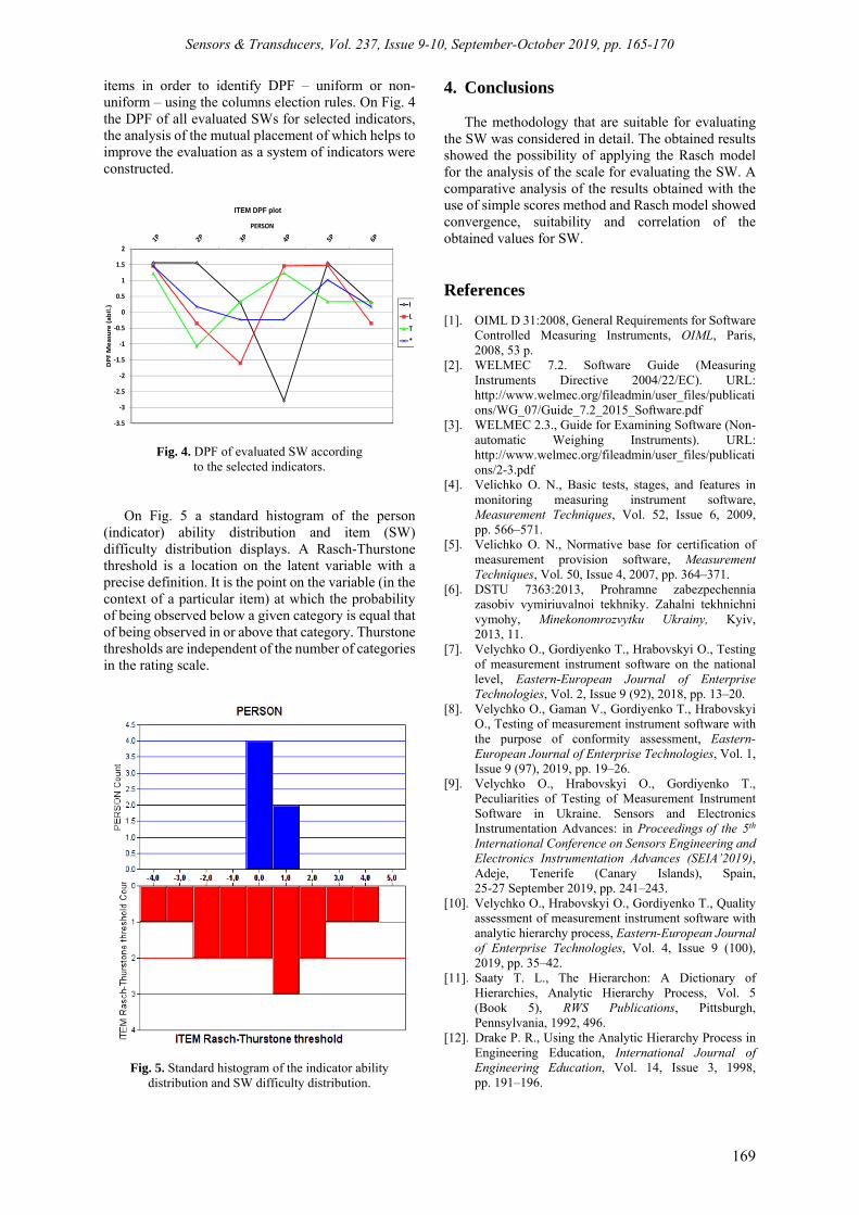
Sensors & Transducers, Vol. 237, Issue 9-10, September-October 2019, pp. 165-170
169
items in order to identify DPF – uniform or non-uniform – using the columns election rules. On Fig. 4 the DPF of all evaluated SWs for selected indicators, the analysis of the mutual placement of which helps to improve the evaluation as a system of indicators were constructed.
Fig. 4. DPF of evaluated SW according to the selected indicators.
On Fig. 5 a standard histogram of the person (indicator) ability distribution and item (SW) difficulty distribution displays. A Rasch-Thurstone threshold is a location on the latent variable with a precise definition. It is the point on the variable (in the context of a particular item) at which the probability of being observed below a given category is equal that of being observed in or above that category. Thurstone thresholds are independent of the number of categories in the rating scale.
Fig. 5. Standard histogram of the indicator ability distribution and SW difficulty distribution.
4. Conclusions
The methodology that are suitable for evaluating the SW was considered in detail. The obtained results showed the possibility of applying the Rasch model for the analysis of the scale for evaluating the SW. A comparative analysis of the results obtained with the use of simple scores method and Rasch model showed convergence, suitability and correlation of the obtained values for SW. References [1]. OIML D 31:2008, General Requirements for Software
Controlled Measuring Instruments, OIML, Paris, 2008, 53 р.
[2]. WELMEC 7.2. Software Guide (Measuring Instruments Directive 2004/22/EC). URL: http://www.welmec.org/fileadmin/user_files/publications/WG_07/Guide_7.2_2015_Software.pdf
[3]. WELMEC 2.3., Guide for Examining Software (Non-automatic Weighing Instruments). URL: http://www.welmec.org/fileadmin/user_files/publications/2-3.pdf
[4]. Velichko O. N., Basic tests, stages, and features in monitoring measuring instrument software, Measurement Techniques, Vol. 52, Issue 6, 2009, pp. 566–571.
[5]. Velichko O. N., Normative base for certification of measurement provision software, Measurement Techniques, Vol. 50, Issue 4, 2007, pp. 364–371.
[6]. DSTU 7363:2013, Prohramne zabezpechennia zasobiv vymiriuvalnoi tekhniky. Zahalni tekhnichni vymohy, Minekonomrozvytku Ukrainy, Kyiv, 2013, 11.
[7]. Velychko O., Gordiyenko T., Hrabovskyi O., Testing of measurement instrument software on the national level, Eastern-European Journal of Enterprise Technologies, Vol. 2, Issue 9 (92), 2018, pp. 13–20.
[8]. Velychko O., Gaman V., Gordiyenko T., Hrabovskyi O., Testing of measurement instrument software with the purpose of conformity assessment, Eastern-European Journal of Enterprise Technologies, Vol. 1, Issue 9 (97), 2019, pp. 19–26.
[9]. Velychko O., Hrabovskyi O., Gordiyenko T., Peculiarities of Testing of Measurement Instrument Software in Ukraine. Sensors and Electronics Instrumentation Advances: in Proceedings of the 5th International Conference on Sensors Engineering and Electronics Instrumentation Advances (SEIA’2019), Adeje, Tenerife (Canary Islands), Spain, 25-27 September 2019, pp. 241–243.
[10]. Velychko O., Hrabovskyi O., Gordiyenko T., Quality assessment of measurement instrument software with analytic hierarchy process, Eastern-European Journal of Enterprise Technologies, Vol. 4, Issue 9 (100), 2019, pp. 35–42.
[11]. Saaty T. L., The Hierarchon: A Dictionary of Hierarchies, Analytic Hierarchy Process, Vol. 5 (Book 5), RWS Publications, Pittsburgh, Pennsylvania, 1992, 496.
[12]. Drake P. R., Using the Analytic Hierarchy Process in Engineering Education, International Journal of Engineering Education, Vol. 14, Issue 3, 1998, pp. 191–196.
-3.5
-3
-2.5
-2
-1.5
-1
-0.5
0
0.5
1
1.5
2
DPF
Mea
sure
(abi
l.)
PERSON
ITEM DPF plot
ILT*

Sensors & Transducers, Vol. 237, Issue 9-10, September-October 2019, pp. 165-170
170
[13]. Rasch G., Probabilistic models for some intelligence and attainment tests, Danish Institution for Educational Research, Copenhagen, 1960, 199 р.
[14]. Andrich D., Rasch models for measurement, Sage Publications, Inc., Newbury Park CA, 1988, 95 р.
[15]. Wright B. D., Linacre J. M., A measurement is the quantification of a specifically defined comparison, Rasch model derived from objectivity, Rasch Measurement Transactions, Vol. 1, Issue 1, 1987, pp. 4–5.
[16]. Bond T. G., Fox C. M., Applying the Rasch model: fundamental measurement in the human sciences,
2nd ed., Lawrence Erlbaum Associates, Mahwah, New Jersey, 2007.
[17]. Velychko O., Gordiyenko T., A comparative analysis of the assessment results of the competence of technical experts by methods of Analytic Hierarchy Process and with using the Rasch model, Eastern-European Journal of Enterprise Technologies, Vol. 3, Issue 3 (93), 2018, pp. 14–21.
[18]. A User’s Guide to WINSTEPS®MINISTEP Rasch-Model Computer Programs. Program Manual 4.4.0 by John M. Linacre, 2019, 704 p.
__________________
Published by International Frequency Sensor Association (IFSA) Publishing, S. L., 2019 (http://www.sensorsportal.com).

Sensors & Transducers, Vol. 237, Issue 9-10, September-October 2019, pp. 171-177
171
Sensors & Transducers
Published by IFSA Publishing, S. L., 2019 http://www.sensorsportal.com
Features of Calibration of Precision LCR Meters
1, * O. VELYCHKO, 2 S. SHEVKUN and 3 M. DOBROLIUBOVA 1, 2 State Enterprise ‘All-Ukrainian State Scientific and Production Centre for Standardization,
Metrology, Certification and Protection of Consumer’, (SE ‘Ukrmetrteststandard’), 4 Metrologichna str., Kyiv, Ukraine
3 National Technical University of Ukraine ‘Igor Sikorsky Kyiv Polytechnic Institute’, 37 Peremogy Ave., Kyiv, Ukraine
Tel.: + 38 044 526 55 68, fax: + 38 044 526 55 68 * E-mail: [email protected]
Received: 30 August 2019 /Accepted: 27 September 2019 /Published: 30 November 2019 Abstract: The features of estimation of the measurement uncertainty at calibration of LCR-meters of precision on the State primary standard of units of inductance and tangent of loss angle, as well as on the State primary standard of units of electric capacitance and factor of loss are presented. The general approaches to calibration of LCR meters and equations (models) of measurements during calibration are presented, as well as details of the calculations of uncertainty of measurements of active resistance, inductance and electrical capacitance for calibration of LCR meters using standard measures. The factors that influence the result of measurements of electrical quantities are considered. The approaches to uncertainty estimation allow calibration of a wide range of LCR meters across a wide frequency range and range of values, and will help create a unified approach to identifying the main components of the measurement model, the uncertainty budget, and the design of calibration results. The materials can be used by laboratories that perform the calibration, testing and conformity assessment of the electromagnetic measuring equipment. The research materials can also be used in conducting international comparisons of reference standards of national metrological institutes and interlaboratory comparisons of measurement results. The research results will help to organize the metrological provision of impedance parameter measurements in many fields of science and technology. Keywords: Uncertainty budget, Measurement, Standard, Calibration, LCR meter, Uncertainty estimation. 1. Introduction
One of the most important tasks for all fields of science and technology involved in the use of electrical measurements is the measurement of inductance, capacitance and active resistance across a wide range of frequencies and values.
The high accuracy and traceability of impedance parameter measurements is essential in such fields as electrical engineering, electronics, machine tools, instrumentation, construction, transportation, telecommunications, metallurgy, mechanical and
aeronautical industries, security, and research and defense [1-4].
Currently, a large number of high-precision reference and impedance measuring instruments are widely used, namely: precision Keysight (Agilent) E4980 AL LCR meters of various modifications, IET/QuadTech 7600 Plus, GW INSTEK LCR-6300, Applent Instruments AT810A, MHC-1100 and MOE-1200, etc. Combined devices and multimeters have become the most widely used in the creation, commissioning and operation of various electronic equipment. They require calibration over a wide
http://www.sensorsportal.com/HTML/DIGEST/P_3126.htm

Sensors & Transducers, Vol. 237, Issue 9-10, September-October 2019, pp. 171-177
172
frequency range and range of values of inductance, electrical capacitance, active resistance.
The purpose of the research is to develop methods of calibration of LCR-meters of precision and other impedance parameter meters, as well as to create a unified approach to determining the main components of the measurement model, uncertainty budget and design of calibration results [5].
2. The Main Content of the Research The vast majority of calibrated precision LCR
meters have the following metrological characteristic: - Measurement ranges at the fundamental
frequency of 1 kHz; - Active resistance R from 1·10E-5 to
1·10E11 Ohms; - Electrical capacitance C from 1·10E-17 to 10 F; - Inductance L from 1·10E-10 to 1·10E8 H; - Loss tangent tgδ from ± 1·10E-6 to ± 1; - Operating frequency range from 0.5 to
1000000 Hz; - The extended relative uncertainty of
measurement of specified parameters at the fundamental frequency and at direct current depending on the range is from 1·10E-3 to 1·10E-5.
Calibration of precision LCR meters in Ukraine is performed with the help of highly stable measures of inductance, electrical capacity and active resistance, which are part of the State primary standard of units of inductance and loss tangent, as well as of State primary standard of units of electric capacity and factor of losses.
These measures have metrological traceability to international standards on fundamental physical constants by calibration or participation in international intelligence [6-13].
Before calibrating the LCR meter, the operating frequency, the measuring voltage, and its automatic self-calibration are set. The LCR meter controls must specify a substitution (capacitance/inductance, parallel/consequent) circuit for the measurement object. If the circuit is incorrectly selected, the overriding value of the main parameter being measured may be very different from the true values.
Before connecting to a LCR meter for a reactive measurements object must be discharged – shorten the contacts for a few seconds. As a rule, the calibration of LCR meters is carried out in terms of: active resistance, electric capacitance and inductance. Sometimes customers who need to use the LCR meter in the most accurate measurements require calibration at operating frequency and loss angle tangent.
2.1. Calibration of LCR Meter for Active Resistance Measurements
For calibration of the LCR-meter for active
resistance measurements, use standard measures from
the set of MAC-2 with nominal values of 0.1 Ohm, 1 Ohm, 10 Ohm, 100 Ohm, 1 kOhm, 10 kOhm, P4015 with nominal value 100 kOhm, P4016 with nominal value 1 MOhm, P4022M1 with nominal value 10 MOhm. The measurement scheme is shown in Fig. 1.
Fig. 1. Scheme for active resistance measurements for calibration of LCR-meter.
For active resistance measurements, the choice of an equivalent substitution scheme is carried out by investigating the dependence of the phase angle tangent tgφ on the frequency of the working signal f.
If tgφ < 0, then the substitution scheme is capacitive. If, with increasing frequency f, the modulus of the phase angle tangent tgφ increases, then the substitution scheme is parallel, if it decreases, it is consistent.
If tgφ > 0, then the substitution scheme is inductive. If, with increasing frequency f, the tangent modulus of the phase angle tgφ increases, the substitution scheme is sequential, if it decreases, it is parallel.
For calibration, n independent measurements of the resistance SR are reproduced; this is reproduced
by a reference measure. The LCR meter reads the
average LCRR .
The equation (model) of measurements has the following form:
LCR LCR S Sf S
QLCR ST TLCR l
R R R R R
R R R R
γΔ = − + Δ + Δ +
+Δ + Δ + Δ + Δ, (1)
where LCRRΔ is the deviation of readings of LCR
meter being calibrated from the true value of the active
resistance reproduced by the reference measure; LCRR
is the mean of the active resistance displayed on the screen of the LCR meter with n measurements of

Sensors & Transducers, Vol. 237, Issue 9-10, September-October 2019, pp. 171-177
173
active resistance of the reference measure; SR is the
value of the active resistance of the reference measure from the calibration certificate; SfRΔ is correction for
frequency dependence of the reference measure of active resistance; SRΔ γ is correction to drift of the
reference measure of active resistance since the last calibration; QLCRRΔ is correction for the quantization
error (sampling) of LCR meter being calibrated; STRΔ
is correction for the temperature dependence of the
reference measure; TLCRRΔ is correction for the
temperature dependence of calibrated LCR meter for the active resistance measurements; lRΔ is correction
for spurious active resistance of connecting cables and contacts.
Based on this measurements model, an example of calculating the uncertainty budget for calibration of LCR meter for active resistance measurements with using a reference measure of 100 Ohms at a frequency of 1 kHz may have the form shown in Table 1.
Table 1. The uncertainty budget for the active resistance measurements of a reference measure of 100 Ohms at 1 kHz for calibration of LCR meter.
Quantity
iX ,
Ohm
Estimate
ix ,
Ohm
Standard uncertainty
( )iu x , Ohm Probability distribution
Method of evaluation
(A, B)
Sensitivity coefficient
ic
Uncertainty contribution
( )iu y , Ohm
LCRR
99.9989 1.45E-04 Normal A 1 1.45E-04
SR 99.9977 1.75E-05 Normal В -1 -1.75E-05
SfRΔ -0.0461 1.10E-05 Normal В 1 1.10E-05
SRΔ γ 0.00001 1.00E-05 Normal В 1 1.00E-05
QLCRRΔ 0 5.77E-05 Rectang. В 1 5.77E-05
STRΔ 0 5.00E-05 Rectang. В 1 5.00E-05
TLCRRΔ 0 1.00E-04 Rectang. В 1 1.00E-04
lRΔ 0 1.00E-04 Normal В 1 1.00E-04
LCRRΔ 0.0012
Combined standard uncertainty 2.17E-04 Effective degrees of freedom neff >200, k = 2 Expanded uncertainty (p ≈ 95 %) 4.34E-04
Type A standard uncertainty associated with a
random component of the estimate is determined by the formula:
( )2
1
1( )
( 1) =
=
= Σ − −
A LCR
n
LCRi LCRj
u R
R Rn n
(2)
The total standard uncertainty of the of active
resistance measurements for calibrating of LCR meter is calculated by the formula:
( )
( ) ( )2 2
1
Σ
=
Δ =
= + Σ Δ
LCR
N
A LCR Bi LCRi
u R
u R u R (3)
Extended uncertainty with coverage factor k = 2
and confidence probability p ≈ 95 %:
( ) ( )2Σ Σ= ⋅ Δ = ⋅ ΔLCR LCRU k u R u R (4)
It will be noted that the above calibration results
correspond to only one measurement point – 100 Ohms at a frequency of 1 kHz. At the same time, the calibration of the meter, which is also LCR meter, must be carried out in the full range of frequencies and values. The only exception is when the calibration range is narrowed at the request of the customer.
Therefore, calibration will be performed at several points (at least three) of each sub-band. It is advisable to give the result of the calibration as a graph depicting the deviation of the LCR meter's readings from the true value of the measured value with its associated measurement uncertainty.
The graph is obtained by approximating the calibration results at the corresponding calibration points. In areas where there may be extremes of the graph, or significant nonlinearity, the number of calibration points should be increased.

Sensors & Transducers, Vol. 237, Issue 9-10, September-October 2019, pp. 171-177
174
2.2. Calibration of LCR Meter for Electrical Capacitance Measurements
For calibration of the LCR-meter for electrical capacitance measurements, the standard thermostatic measures of the Andeen-Hagerling type AH11A of 10 pF and 100 pF from the State primary standard of units of capacitance and loss factor, thermostated capacitance store and resistances, and capacities are used as standard. P597 rated at 1 pF, 10 pF, 100 pF and others. The measurement scheme is shown in Fig. 2.
Fig. 2. Scheme for electrical capacitance measurements for calibration of LCR meter.
For capacitance measurements by LCR meter, the choice of an equivalent substitution scheme is carried out by research the dependence of the loss angle tgδ on the frequency f. If, with increasing frequency f, the loss tangent modulus tgδ increases, then the replacement scheme is sequential, if it decreases, it is parallel.
For example, consider the calibration of an LCR meter for electric capacitance measurements using a 100 pF Andeen-Hagerling type AH11A-type thermostatized reference electrical capacitance standard.
The equation (model) of measurements has the following form:
γΔ = − + Δ + Δ +
+Δ + Δ + Δ + ΔLCR LCR S Sf S
QLCR ST TLCR l
С С С С C
C C C C , (5)
where LCRСΔ is the deviation of the readings of LCR
meter being calibrated from the true value of the inductance reproduced by the reference measure;
LCRС is the average value of capacitance displayed on
the screen of LCR-meter for the capacitance
measurements of the reference measure; SС is the
value of the reference measure capacitance from the calibration certificate; SfCΔ is correction of
frequency dependence of the reference measure of capacitance; SСΔ γ is correction to drift of the
reference capacity measure since the last calibration;
QLCRСΔ is correction for the quantization error of
LCR meter being calibrated; STСΔ is correction for
the temperature dependence of the reference measure;
TLCRСΔ is correction for the temperature dependence
of the calibrated LCR meter; lСΔ is correction for
spurious capacitance of connecting cables and contacts.
Based on this measurement model, an example of calculating the uncertainty budget for calibration of LCR meter for capacitance measurements with using a reference measure of 100 pF at a frequency of 1 kHz may have the form shown in Table 2.
Type A standard uncertainty associated with a random component of the estimate LCRC is
determined by the formula:
( )2
1
1( )
( 1)
A LCR
n
LCRi LCRj
u С
С Сn n =
=
= Σ − −
(6)
The total standard uncertainty of the capacitance
measurements for calibration of LCR meter is calculated by the formula:
( )
( ) ( )2 2
1
LCR
N
A LCR Bi LCRi
u С
u С u С
Σ
=
Δ =
= + Σ Δ (7)
Extended uncertainty with coverage factor k = 2
and confidence probability p ≈ 95 %:
( ) ( )2LCR LCRU k u С u СΣ Σ= ⋅ Δ = ⋅ Δ (8)
2.3. Calibration of LCR Meter for Electrical Inductance Measurements
For calibration of the LCR-meter for electrical
inductance measurements, the standard thermostatized measures of inductance P5113 of the State primary standard of units of inductance and loss tangent of nominal 1 mH, 10 mH, 100 mH, and reference measures P593, P596, P5101 with a value from 0.01 µH to 100 mH and others. Diagrams of measurements at 2-pin and 3-pin connection are shown in Fig. 3 and Fig. 4.

Sensors & Transducers, Vol. 237, Issue 9-10, September-October 2019, pp. 171-177
175
Table 2. The uncertainty budget for the electrical capacitance measurements of a reference measure of 100 pF at 1 kHz for calibration of LCR meter.
Quantity
iX
Estimate
ix , pF
Standard uncertainty
( )iu x , pF Probability distribution
Method of evaluation
(A, B)
Sensitivity coefficient
ic
Uncertainty contribution
( )iu y , pF
LCRС
100.00008 1.47E-05 Normal A 1 1.47E-05
SС 100.00014 4.00E-05 Normal В -1 -4.00E-05
SfСΔ 0.00008 1.00E-05 Normal В 1 1.00E-05
SСΔ γ -0.00001 4.00E-05 Normal В 1 4.00E-05
QLCRСΔ 0 5.77E-05 Rectang. В 1 5.77E-05
STСΔ 0 1.90E-04 Rectang. В 1 1.90E-04
TLCRСΔ 0 1.00E-04 Rectang. В 1 1.00E-04
lСΔ 0 1.00E-04 Normal В 1 1.00E-04
LCRСΔ -0.00007
Combined standard uncertainty 2.51E-04 Effective degrees of freedom neff >200, k = 2 Expanded uncertainty (p ≈ 95 %) 5.01E-04
Fig. 3. Scheme for inductance measurements for calibration of LCR-meter (2-pin connection).
Fig. 4. Scheme for inductance measurements
for calibration of LCR-meter (3-pin connection).
For inductance measurement by LCR meter, the
choice of an equivalent substitution scheme is made by investigating the dependence of the loss tangent tgδ on the frequency f. If, with increasing frequency f, the loss tangent modulus tgδ increases, then the substitution scheme is parallel, if it decreases, it is consistent.
For example, consider the calibration of LCR meter for inductance measurements with using the thermostated precision standard 100 mH of P5113 [14].
The equation (model) of measurements has the following form:
γΔ = − + Δ + Δ +
+Δ + Δ + Δ + ΔLCR LCR S Sf S
QLCR ST TLCR l
L L L L L
L L L L, (9)
where LCRLΔ is the deviation of the readings of LCR
meter being calibrated from the true value of the
inductance reproduced by reference measure; LCRL is
the average value of the inductance displayed on the screen of LCR meter for inductance measurements of reference measure; SL is the value of inductance of
the reference measure from the calibration certificate;
SfLΔ is correction for frequency dependence of the

Sensors & Transducers, Vol. 237, Issue 9-10, September-October 2019, pp. 171-177
176
standard measure of inductance; SL γΔ is correction to
drift of the reference measure of inductance since the last calibration; QLCRLΔ is correction for the
quantization error of the LCR meter being calibrated;
STLΔ is correction for the temperature dependence of
reference measure; TLCRLΔ is correction for the
temperature dependence of the calibrated LCR meter;
lLΔ is correction for spurious inductance of
connecting cables and contacts. Based on this measurements model, an example of
calculating the uncertainty budget for calibration an LCR meter for inductance measurements with using a reference measure of 100 mH at 1 kHz may be as shown in Table 3.
Table 3. The uncertainty budget for the electrical capacitance measurements of a reference measure of 100 mH at 1 kHz for calibration of LCR meter.
Quantity
iX
Estimate
ix ,
mH
Standard uncertainty
( )iu x , mH Probability distribution
Method of evaluation
(A, B)
Sensitivity coefficient
ic
Uncertainty contribution
( )iu y , mH
LCRL 100.1100 3.52E-04 Normal A 1 3.52E-04
SL 100.0082 4.00E-04 Normal В -1 -4.00E-04
SfLΔ
0.0001 1.00E-05 Normal В 1 1.00E-05
SL γΔ 0 1.10E-05 Normal В 1 1.10E-05
QLCRLΔ 0 5.77E-05 Rectang. В 1 5.77E-05
STLΔ 0 3.60E-05 Rectang. В 1 3.60E-05
TLCRLΔ 0 1.00E-04 Rectang. В 1 1.00E-04
lLΔ 0 1.00E-04 Normal В 1 1.00E-04
LCRLΔ 0.1018
Combined standard uncertainty 5.56E-04 Effective degrees of freedom neff >200, k = 2 Expanded uncertainty (p ≈ 95 %) 1.11E-03
Type A standard uncertainty associated with a
random component of the estimate LCRL is
determined by the formula:
( )2
1
1( )
( 1)
A LCR
n
LCRi LCRj
u L
L Ln n =
=
= Σ − −
(10)
The total standard uncertainty of inductance
measurements for calibration of LCR meter is calculated by the formula:
( )
( ) ( )2 2
1
Σ
=
Δ =
= + Σ Δ
LCR
N
A LCR Bi LCRi
u L
u L u L (11)
Extended uncertainty with coverage factor k = 2
and confidence probability p ≈ 95 %:
( ) ( )2Σ Σ= ⋅ Δ = ⋅ ΔLCR LCRU k u L u L (12)
For calibration of LCR meter, the results of
measurements and the uncertainty budget are
calculated in the same order by such values as operating frequency f, phase angle tgφ, loss angle tgδ, and other impedance parameters.
3. Conclusions
As a result of the conducted researches the method of calibration of LCR-meters on the State primary standard of units of inductance and tangent of loss angle and the State primary standard of units of electric capacitance and factor of loss was developed. The technique fully enables the calculation of calibration results and the uncertainty budget for the calibration of LCR meters, multimeters, and combined devices by such values as inductance, electrical capacitance, and active resistance over the full frequency range and values.
In order to achieve high accuracy of impedance parameter measurements, it is of great importance to choose an equivalent circuit (capacitance/ inductance, parallel/consequent) for the measurement object.
For active resistance measurements by LCR meter, the choice of an equivalent substitution scheme is carried out by studying the dependence of the phase angle tangent tgφ on the frequency of the working signal f, and for electrical capacitance or inductance

Sensors & Transducers, Vol. 237, Issue 9-10, September-October 2019, pp. 171-177
177
measurements are depending on the frequency f the tangents of the loss angle tgδ.
Uncertainty estimation approaches can be used in conducting international reconciliation of reference standards of national metrology institutes and interlaboratory comparisons of measurement results. The research results will help to organize the metrological provision of impedance parameter measurements in all fields of science and technology.
References [1]. ДСТУ ISO/IEC 17025:2017, General requirements
for the competence of testing and calibration laboratories, Derjspojivstandart of Ukraine, 2017.
[2]. O. Velychko, S. Shevkun, A support of metrological traceability of inductance measurements in Ukraine, Eastern-European Journal of Enterprise Technologies. Information and controlling systems, Vol. 5/9, Issue 89, 2017, pp. 12–18.
[3]. O. Velychko, S. Shevkun, Support of metrological traceability of capacitance measurements in Ukraine, Eastern-European Journal of Enterprise Technologies. Information and controlling systems, Vol. 3/9, Issue 87, 2017, pp. 4–10.
[4]. O. Velychko, S. Shevkun, T. Gordiyenko, M. Dobroliubova, Metrological traceability of impedance parameter measurements in Ukraine, Eastern-European Journal of Enterprise Technologies. Information and Controlling Systems, Vol. 4/9, Issue 94, 2018, pp. 43–49.
[5]. ISO/IEC Guide 98–3:2008, Uncertainty of measurement. Part 3. Guide to the expression of uncertainty in measurement, ISO/IEC, 2008.
[6]. O. Velychko, S. Shevkun, Final Report on COOMET supplementary comparison of inductance at 10 mH and 100 mH at 1 kHz (COOMET.EM-S14), Metrologia, Vol. 53, Issue 1A, Technical Supplement, 2016, 01009.
[7]. E. Dierikx, et. al., Final report on the supplementary comparison EURAMET.EM-S26: inductance measurements of 100 mH at 1 kHz (EURAMET project 816), Metrologia, Vol. 49, 2012, 01002.
[8]. O. Velychko, O. Akhmadov, Final report on COOMET key comparison of capacitance at 10 pF (COOMET.EM-K4), Metrologia, Vol. 54, Issue 1A, 2017, 01005.
[9]. O. Velychko, O. Akhmadov, Final Report on COOMET Supplementary Comparison of Capacitance at 100 pF (COOMET.EM-S4), Metrologia, Vol. 54, Issue 1A, 2017, 01006.
[10]. O. Velychko, S. Shevkun, Final Report on COOMET Supplementary Comparison of Capacitance at 10 pF and 100 pF (COOMET.EM-S13), Metrologia, Vol. 53, Issue 1A, 2014, 01009.
[11]. O. Velychko, S. Shevkun, J. Bartholomew, A. Alrobaish, Final Report on GULFMET Supplementary Comparison of Inductance at 10 mH and 100 mH at 1 kHz (GULFMET. EM-S4), Metrologia, Vol. 56, Issue 1A, 2019, 01013.
[12]. O. Velychko, Possibilities of Linking Results of Key and Supplementary Comparisons in Field of Electricity and Magnetism, Measurement, Vol. 144, 2019, pp. 167–172.
[13]. O. Velychko, T. Gordiyenko, Metrological Traceability at Different Measurement Levels, Standards, Methods and Solutions of Metrology, Edited by Luigi Cocco, Published in London, IntechOpen, UK, October, 2019, pp. 1-21.
[14]. Iu. Kuzmenko, O. Velychko, S. Shevkun, M. Dobroliubova, Estimation of Uncertainty in Calibration of Precision LCR-meters on the State Primary Standard of Units of Inductance and Tangent Angles of Losses, in Proceedings of the 5th International Conference on Sensors and Electronic Instrumentation Advances (SEIA’2019), Adeje, Tenerife (Canary Islands), Spain, 25-27 September 2019, pp. 331-332.
__________________
Published by International Frequency Sensor Association (IFSA) Publishing, S. L., 2019 (http://www.sensorsportal.com).

Aims and Scope
Sensors & Transducers is established, international, peer-reviewed, open access journal (print and electronic). It provides the best platform for the researchers and scientist worldwide to exchange their latest findings and results in science and technology of physical, chemical sensors and biosensors. The journal publishes original results of scientific and research works related to strategic and applied studies in all aspects of sensors: reviews, regular research and application specific papers, and short notes. In comparison with other sensors related journals, which are mainly focused on technological aspects and sensing principles, the Sensors & Transducers significantly contributes in areas, which are not adequately addressed in other journals, namely: frequency (period), duty-cycle, time-interval, PWM, phase-shift, pulse number output sensors and transducers; sensor systems; digital, smart, intelligent sensors and systems designs; signal processing and ADC in sensor systems; advanced sensor fusion; sensor networks; applications, etc. By this way the journal significantly enriches the appropriate databases of knowledge.
Sensors & Transducers journal has a very high publicity. It is indexed and abstracted very quickly by Chemical Abstracts, EBSCO Publishing, IndexCopernicus Journals Master List (ICV=6.13 in 2011), ProQuest Science Journals, CAS Source Index (CASSI), Ulrich's Periodicals Directory, Scirus, Google Scholar, etc. Since 2011 to 2014 Sensors & Transducers journal was covered and indexed by EI Compendex (CPX) index (including a Scopus, Embase, Engineering Village and Reaxys) in Elsevier products. The journal is included in the IFSA List of Recommended Journals (up-dated 9.12.2015), which contains only the best, established sensors related journals.
Topics of Interest
Include, but are not restricted to: Physical, chemical sensors and biosensors Digital, frequency, period, duty-cycle, time interval, PWM, pulse number output sensors and transducers
Theory, principles, effects, design, standardization and modelling Smart sensors and systems Intelligent sensors and systems Sensor instrumentation Virtual instruments Sensors interfaces, buses and networks Signal processing, sensor fusion Remote sensing Frequency (period, duty-cycle)-to-code converters, ADC Technologies and materials Nanosensors and NEMS Microsystems Applications
Further information on this journal is available from the Publisher's web site: http://www.sensorsportal.com/HTML/DIGEST/New_Digest.htm
Free Access and Subscriptions
Sensors & Transducers is the open access journal. All single articles are available for free download (article by article) without any registration and embargo period. For those who want to get the full page journal issue in print and/or pdf format there is an annual subscription. It includes 12 regular issues and some special issues. Annual subscription rates for 2016/2017 are the following: Electronic version (in printable pdf format): 590.00 EUR; Printed with b/w illustrations: 950.00 EUR; 15 % discount is available for IFSA Members.
Further information about subscription is available on the IFSA Publishing's web site: http://www.sensorsportal.com/HTML/DIGEST/Journal_Subscription.htm
Advertising Information
If you are interested in advertising or other commercial opportunities please download our Media Planner 2016: http://www.sensorsportal.com/DOWNLOADS/Media_Planner_2016.pdf
Instructions for Authors
http://www.sensorsportal.com/HTML/DIGEST/Guides_for_Authors.htm