
Selecting appropriate calibration points for an ultra low area 8-bit subrange ADC
6
Selecting Appropriate Calibration Points for an Ultra Low Area 8-bit Subrange ADC Nikos Petrellis, Michael Birbas, John Kikidis and Alexios Birbas Analogies SA., Patras Science Park, Platani-Rio, Patras, Greece [email protected] Abstra-An ultra low area 8-bit subrange AnaloguelDigital Converter that consists of a pair of Flash 4-bit converter stages is described in this paper emphasising on the appropriate method for its real time calibration. Its active area occupies only 0.04 mm 2 and dissipates less than 22 mW. The sampling rate is higher than 500 MS/s and the achieved Signal to Noise and Distortion Ratio is higher than 40 dB. A voltage mode integer divider is used at the input of this AnaloguelDigital Converter driving the two output Flash stages by its quotient and residue. The ultra low area and power is owed to the use of the integer divider at the input stage of the subrange converter and the employment of a "thermometer to binary encoder" instead of a full 4-bit Flash AnaloguelDigital Converter for the generation of the 4 most significant bits. The calibration method employed for this AnaloguelDigital Converter is based on the proper biasing of the resistor ladders used by the fine 4-bit Flash stage as well as on properly delaying and shifting of the divider signals that generate the residue. I. INTRODUCTION Flash Analog/Digital Converters (ADCs) achieve the highest conversion speed since the input signal (either voltage or current) is concurrently compared to 2 ° reference levels. The 2 ° comparator outputs form a "thermometer code" that is converted to the n-bit binary output. A resolution higher than 7-bits is difficult to be achieved with Flash chitecture since the large number of the compators employed requires excessively large area and power consumption. Multi GS/s throughput is achieved using Flash architectures with special techniques [I], expensive technologies [2] or multiple (slower) ADCs that operate in a time interleaved fashion [3]. Flash ADCs, non-linearity problems are caused by the mismatches in the resistors used in the resistor ladder and by the offset of the comparators. These mismatches affect only the corresponding comparison level and consequently the linearity of a single output code and thus multiple eors are not accumulated. Pipeline [4][5] and Subrange ADCs [6][7] consist of two or more constituent ADCs that operate concuently. In pipeline ADCs the ADC stages operate on successive samples that are latched by intermediate Track and Hold circuits while in subrange (or subfolder) architectures the constituent ADC stages operate on the same input sample and the overall output is valid when the slower path is settled. In both pipeline and subrange ADCs the coarse stage produces the most significant bits while the fine one generates the least significant bits. In this way, the area is reduced while the throughput becomes comparable to that of a flash ADC that has the same resolution. For example, a two stage n-bit pipelined ADC may 978-1-425716-8/1026.00 ©2010 IîE consist of two n!2-bit flash ADCs that require only 2 2 + 1 comparators. The disadvantage of a pipeline ADC is that its latency for a single sample conversion is multiple times higher than that of a pipeline ADC. In pipeline or subrange ADCs non linearity is also introduced by the circuits that convert the coarse digital ADC output to an analogue value that is subtracted by the input signal in order to produce the residue that serves as input to the fine ADC stage. For this reason, Digital to Analogue Converters (DAC) with high linearity have to be used in conjunction with circuits that are immune to component mismatches and temperature variations in order to provide a valid input to the fine ADC stage. Various techniques have been proposed in the literature for the real time calibration and the minimisation of the non- linearity effects of ADCs. A popular error correction technique used in pipelined ADCs exploits the least significant bits of the coarse ADC for eor detection d correction. For example, in [8] a 1O-bit ADC is constructed by a 4-bit coarse and a 7-bit fine ADC. The least significant bit of the coarse ADC should match the most significant bit of the fine ADC. [9] eight 1.5-bit stages followed by one 2-bit Flash ADC are used in a 10-bit pipelined ADC architecture. Component mismatches can be handled by inserting redundancy as is the case in [10] where an additional aay of capacitors is used for real time trimming that is performed by an on-chip algorithm in order to handle component aging. The interconnection of the additional capacitors is controlled by non volatile memory cells. A digital calibration of the capacitor mismatch, the comparator offsets and the charge injection offsets in a pipelined ADC is performed in [11] for the improvement of DNL errors. The biasing of the operational amplifiers used in a pipelined ADC according to the power supply, the temperature variations and the sampling speed is determined by calibration in [4]. The offset of the residue amplifiers is calibrated in the background in [12] in order to avoid interruption of the normal ADC operation. A two stage subrange voltage mode ADC is presented in this paper that is based on a novel integer divider circuit the quotient and the residue of which are used as inputs to a pair of 4-bit ADCs (a coarse and a fine one). The integer divider incoorates 15 comparators that are also part of the 4-bit coarse ADC. Since these comparators are not duplicated in the 4-bit coarse ADC, the area and the power required by the 8-bit ADC is extremely low. The residue of the integer divider is input to a ll 4-bit Flash ADC.
-
Upload
independent -
Category
Documents
-
view
0 -
download
0
Transcript of Selecting appropriate calibration points for an ultra low area 8-bit subrange ADC

Selecting Appropriate Calibration Points for an Ultra Low Area 8-bit Subrange ADC
Nikos Petrellis, Michael Birbas, John Kikidis and Alexios Birbas Analogies S.A., Patras Science Park, Platani-Rio, Patras, Greece
Abstract-An ultra low area 8-bit subrange AnaloguelDigital Converter that consists of a pair of Flash 4-bit converter stages is described in this paper emphasising on the appropriate method for its real time calibration. Its active area occupies only 0.04 mm2 and dissipates less than 22 mW. The sampling rate is higher than 500 MS/s and the achieved Signal to Noise and Distortion Ratio is higher than 40 dB. A voltage mode integer divider is used at the input of this AnaloguelDigital Converter driving the
two output Flash stages by its quotient and residue. The ultra low area and power is owed to the use of the integer divider at the input stage of the subrange converter and the employment of a "thermometer to binary encoder" instead of a full 4-bit Flash
AnaloguelDigital Converter for the generation of the 4 most significant bits. The calibration method employed for this AnaloguelDigital Converter is based on the proper biasing of the resistor ladders used by the fine 4-bit Flash stage as well as on
properly delaying and shifting of the divider signals that generate the residue.
I. INTRODUCTION
Flash Analog/Digital Converters (ADCs) achieve the highest conversion speed since the input signal (either voltage or current) is concurrently compared to 2° reference levels. The 2° comparator outputs form a "thermometer code" that is converted to the n-bit binary output. A resolution higher than 7-bits is difficult to be achieved with Flash architecture since the large number of the comparators employed requires excessively large area and power consumption. Multi GS/s throughput is achieved using Flash architectures with special techniques [I], expensive technologies [2] or multiple (slower) ADCs that operate in a time interleaved fashion [3]. In Flash ADCs, non-linearity problems are caused by the mismatches in the resistors used in the resistor ladder and by the offset of the comparators. These mismatches affect only the corresponding comparison level and consequently the linearity of a single output code and thus multiple errors are not accumulated.
Pipeline [4][5] and Subrange ADCs [6][7] consist of two or more constituent ADCs that operate concurrently. In pipeline ADCs the ADC stages operate on successive samples that are latched by intermediate Track and Hold circuits while in subrange (or subfolder) architectures the constituent ADC stages operate on the same input sample and the overall output is valid when the slower path is settled. In both pipeline and subrange ADCs the coarse stage produces the most significant bits while the fine one generates the least significant bits. In this way, the area is reduced while the throughput becomes comparable to that of a flash ADC that has the same resolution. For example, a two stage n-bit pipe lined ADC may
978-1-4244-5716-8/10/$26.00 ©20 10 IEEE
consist of two n!2-bit flash ADCs that require only 2n12+1
comparators. The disadvantage of a pipeline ADC is that its latency for a single sample conversion is multiple times higher than that of a pipeline ADC.
In pipeline or subrange ADCs non linearity is also introduced by the circuits that convert the coarse digital ADC output to an analogue value that is subtracted by the input signal in order to produce the residue that serves as input to the fine ADC stage. For this reason, Digital to Analogue Converters (DAC) with high linearity have to be used in conjunction with circuits that are immune to component mismatches and temperature variations in order to provide a valid input to the fine ADC stage.
Various techniques have been proposed in the literature for the real time calibration and the minimisation of the nonlinearity effects of ADCs. A popular error correction technique used in pipe lined ADCs exploits the least significant bits of the coarse ADC for error detection and correction. For example, in [8] a 1O-bit ADC is constructed by a 4-bit coarse and a 7-bit fine ADC. The least significant bit of the coarse ADC should match the most significant bit of the fine ADC. In [9] eight 1.5-bit stages followed by one 2-bit Flash ADC are used in a 10-bit pipe lined ADC architecture.
Component mismatches can be handled by inserting redundancy as is the case in [10] where an additional array of capacitors is used for real time trimming that is performed by an on-chip algorithm in order to handle component aging. The interconnection of the additional capacitors is controlled by non volatile memory cells. A digital calibration of the capacitor mismatch, the comparator offsets and the charge injection offsets in a pipelined ADC is performed in [11] for the improvement of DNL errors. The biasing of the operational amplifiers used in a pipe lined ADC according to the power supply, the temperature variations and the sampling speed is determined by calibration in [4]. The offset of the residue amplifiers is calibrated in the background in [12] in order to avoid interruption of the normal ADC operation.
A two stage subrange voltage mode ADC is presented in this paper that is based on a novel integer divider circuit the quotient and the residue of which are used as inputs to a pair of 4-bit ADCs (a coarse and a fine one). The integer divider incorporates 15 comparators that are also part of the 4-bit coarse ADC. Since these comparators are not duplicated in the 4-bit coarse ADC, the area and the power required by the 8-bit ADC is extremely low. The residue of the integer divider is input to a full 4-bit Flash ADC.

A current mode integer divider circuit and an innovative ADC architecture based on a binary tree structure have been proposed by the authors in [13]. Although operations like addition, multiplication by a constant etc, are implemented by simple circuits in such a current mode architecture, the difficulty in equalising the delay of the quotient and the residue current paths leads to lower conversion rates. The ability of path delay equalisation in the voltage mode implementation of the integer divider that is presented in this paper allows higher conversion rates to be achieved. Nevertheless, the voltage mode implementation approach is more sensitive to component mismatches than the current mode one. For this reason, a proper calibration method has been studied in detail and applied to the developed subrange ADC.
The rest of the paper is organized as follows: a description of the 8-bit subrange ADC architecture emphasising on the incorporated voltage mode integer divider is presented in Section 2. The Monte Carlo simulation results shown in Section 3 are used to propose an appropriate calibration method. Finally, the ADC along with a comparison with similar implementations are presented in Section 4.
II. 8-BIT SUBRANGE ADC
, I I I
+ 12J Vo
, ,
,
Yin
Rl
R3
lcom
Ycom
Fig. 1. The differential amplifier with common input voltage used by the integer divider.
The integer divider used at the input of the developed 8-bit subrange ADC is based on the circuit of Fig. 1. The inputs of the differential amplifier are connected through R3 and Rptot to the common voltage Vcom and the output is Vo=Vo+-Vo-. The resistance Rptot consists of a number of parallel elementary resistors that are connected in parallel according to
the value of the input voltage Yin. If Yin is within the following limits:
qVref:::; Vin < (q + l)Vref (1)
then the circuit of Fig. 1 implements the integer division VinNref if Vo=qVref. The parameter q represents the quotient of the division as multiples of Vref. The residue of the division can be derived by subtracting Vo from Yin.
In order to analyse how the described division can be implemented using the circuit of Fig. 1, the laws of Kirchoff and Ohm are applied:
leom = (11-11') + (12 -12')
Vee = Veom + 11'(R2 + R3) + 11Rl
Vee = Veom + 12'(R2 + Rptot) + 12Rl
Vo = Vee -11Rl-(Vee -12Rl) = Rl(12 -11)
Vo = Veom + 11'(R2 + R3) -(Veom + 12'(R2 + Rptot) =
11'(R2 + R3) -12'(R2 + Rptot)
(2) (3) (4) (5)
(6)
If we consider as unknowns the currents II, II', 12 and 12' then equations (2)-(6) can be repeatedly solved for defining the resistance Rptot by setting specific output voltage values: Vo is selected successively as Vref, 2Vref, 3Vref, etc, for quotients q=l, 2, 3, etc, respectively and the corresponding Rptot values are estimated during the ADC design time. In order to generate the estimated Rptot as a function of the input voltage Yin as dictated by relation (1), the circuit shown in the dotted line of Fig. 2 is used.
Y..� ........ Y.: ........
..................................................... \
Rptot i �com : I
j' 4 Most Significant Bits
i by 16 +
;"... .......... ........................................................................................ Delay
Fig. 2. The 8-bit subrange ADC.
The input voltage Yin is a differential one (V+ -V") that is compared concurrently to Vref, 2Vref, 3Vref, etc. The outputs of the differential comparators connect different resistors in

parallel in order to form the desired Rptot that was estimated by solving the equations (2)-(6). More specifically, if the resistances estimated for Vo=qVref and Vo'=(q+l)Vref are Rptot and Rptot' respectively, then the resistance Rp that has to be connected in parallel to Rptot for generating Yo' is:
Rp = RptotR' ptot f(R' ptot -Rptot) (7)
Although that the Vo output could have been used as input to a full 4-bit Flash coarse ADC identical to the 4-bit fine one, this would introduce redundancy and additional distortion since the divider comparator outputs can be directly used as input to a "thermometer to binary" encoder that generates the most significant bits.
One of the divider differential outputs (e.g., Yo") can be subtracted from the corresponding input (V") in order to generate the residue of the division. These signals (Vo·, V·) are subject to appropriate amplification, level shifting and delay compensation by the calibration algorithm before they are subtracted so as to be properly aligned in terms of both time and voltage level. The level shifting and the delay compensation required can be implemented by using the circuit of Fig. 3. Vcc
Vo' -1 v'
T3
Vso' To
��� Vh'-1
Vh2-1 4
Fig. 3. Delay compensation and level shifting.
More specifically, the signal V· is delayed by the capacitors that can be connected in parallel by the calibration algorithm through the switches SO, SI and S2 according to the input signal frequency. Four different capacitor combinations can be formed using the three capacitors of Fig. 3 (0 to 3C). More combinations and higher delay precision can be achieved if capacitors with different value (e.g., C, 2C, 4C etc) are combined in parallel. This solution is more precise but would require a more complicated background calibration logic that would be capable of distinguishing a large number of input signal frequency ranges. The level shifting of either Vo· or V· is accomplished by the proper biasing of T2 and T4. If we focus on the level shifting of Vo· the following equations can be derived:
Idsl = Ids2 =>
1 WI 2 1 W2 2 -K-(VgsI-Vthl) =-K-(Vgs2-Vth2) 2 Ll 2 L2
2 2 Vso - = Vo -
W2 L1 (Vbl-Vth2)2 -Vthl
W12 L22
(9)
(10)
In equations (8)-(10) the transistors are assumed to operate in saturation and the Early effect has been ignored. The parameters W, L, Vgs, Ids and Vth are the width, length, the gate-source voltage, drain-source current and the threshold of the transistors respectively. By choosing appropriate W, L transistor sizes the calibration algorithm can control one of Vb 1 or Vb2 in real time in order to perform the proper level shifting.
III. SIMULATION RESULTS AND CALIBRATION METHOD
500 I I I
::�,�. I ""1:-..• I
450
400 �;':'J);._. I ;;-5350 >
300
250
200 o
"�'t,o I r,'·i
fe_._, i �'"
I I I I I
I I I
I .250
I I I I I
I I I
I I -: ..
I ..r 'l:'�� •. }.' .. I .".�
r'":� or'
I
I I I
I .500
time (us)
(a)
I I I I ../:(: I
I :.{:{-r. I . . {'� ·t4 . .Ii'
•• ..!,I
,'1 I I I I I
I I I
I .750 1.0
750f======f=====r=====f=======Jl
;;-5600+-<.i--hic-l--t-++-:!--i--!H-!.-f-+-t-+--,-+""";-+-i:-+-tl-+-+.--+.-+-if.-t-H >
o .500 1.0 time (us)
(b)
1.5
Fig. 4. Subtractor inputs (a) and differential division residue (b).
2.0
(8) The simulated inputs of the subtractor under typical conditions for a full scale 500 kHz triangular input signal are shown in Fig. 4a. The triangular line is the input V· while the

ladder-like curve is one of the differential quotient signals (Vo) The signal V- has been delayed by a configurable MOS capacitance while Vo- has been derived after appropriate amplification and level shifting_ The differential quotient, that is the difference of Vo- and V-, appears in Fig_ 4b and serves as input to the Flash ADC that generates the 4 least significant bits. The bias of this 4-bit Flash ADC can be estimated from Fig. 4b but the amplitude of these curves depends on the input signal frequency. For example, the optimal bias amplitude for input frequencies 2, 5 and 10 MHz are 200, 100 and 50 m V respectively. Although for intermediate frequencies an intermediate biasing would also be more appropriate, 4 biasing levels selected by the calibration algorithm are adequate as proposed in Table I.
TABLEr 4-BIT FLASH ADC LADDER BIAS
Input Frequency 4bit Flash ADC Resistor Ladder Bias
<2 MHz 200 mV 2-4 MHz 150 mV 4-8 MHz 100 mV >8 MHz 50 mV
Vee
so --------
I
Sl
rp+
.... ___ *-----1 ____ 1 rn-
4-LSB Flash ADC
rn+
Common VOuagA�t---prplimit (e.g .. 600mV)
Fig. 5. Bias selection of the 4-bit Flash ADC.
The selection of the appropriate biasing shown in Table I is performed by the resistor ladder like circuit presented in Fig. 5. Since the 4-bit Flash ADC accepts as input a differential signal that is compared to differential levels, two internal resistor ladders have to be biased: the resistor ladder that generates the references for the positive input (biased by Vrp+, Vrp-) and the one that produces the references for the negative input (biased by Vrn+, Vrn-). Vrn+ and Vrp- are connected to the same common bias voltage which is 600 m V for the case shown in Fig. 4b. The smallest bias value is applied if all the SO-S2 switches are open (used with high input frequencies). If one or more of these switches is closed some resistors are
shortcut and a higher biasing value is applied (for lower input frequencies). The value of the resistors used in Fig. 5 is the highest possible for achieving low current leakage.
As already mentioned the other ADC points that should be appropriately controlled by the calibration algorithm are the level shifting of Vo- and the delaying of V-. In other words the calibration algorithm should control the switches SO, Sl, S2 and the voltages Vbl of Fig. 3. Fig. 6 shows why level shifting is important.
600,--------,-----,-----.-------,
.250 .500 time (us)
(a)
.750 1.0
500,--------,-----,-----.-------,
.250 .500 time (us)
(b)
.750 1.0
Fig. 6. Five runs of Monte Carlo simulation of Yo' with resistors of 2um width (a) and 3 or 4um width (b).
The curves presented in Fig. 6 are similar to the ones of Fig. 4a and have been derived from a demonstrative 5-run Monte Carlo simulation for process and mismatch variations using the default values of the Cadence Spectre simulator. It is obvious that the signal Vo- has been significantly shifted up and down away from V- (the triangular line). Moreover, the height and width of the taps is not identical as was the case in Fig. 4a. The latter is due to transistor and resistor mismatches of the integer divider. The increase of the size of these components would improve significantly the mismatch immunity of the system. Nevertheless, the speed of the system would be reduced if the length of the transistors was increased. For this reason, only the resistor width is increased to 3u with

a small penalty in the required die area since the length of the resistors has also to be increased accordingly. In this way, the improved Monte Carlo simulation of Fig. 6b is derived. Further correction of the resistor mismatches for achieving higher linearity can be achieved by well known resistor trimming techniques similar to the ones presented in [10]. Such a correction of the resistor values is required only once after chip fabrication since it does not depend on the input signal frequency, the temperature etc.
The circuit described in Fig. 3 can be used for the appropriate adjustment of the level shifting of Yo" so as to be aligned with V". This is important in order to let these residue curves share a common cross voltage level (600 mY in this case) like the ones shown in Fig. 4b although their amplitude may differ according to the input signal frequency as described in Table I. The switches of Fig. 3 can be controlled by the calibration circuit of Fig. 7 that uses this common cross voltage level as a target for a successful level shifting. Specifically, when calibration starts, the D flip flop is cleared disabling the down counter that is preset in order to set its output the highest value. This value is converted to an analogue one by a simple DAC[13] which is used as a bias voltage for level shifting (e.g., Yb1 of Fig. 3). Applying a high voltage to Yb1 shifts Yo" in such a way so that the curves of Fig. 4b are moved away from each other and the comparator output of Fig. 7 is set. The output of the D flip flop is also set, enabling down counting. The counter output and consequently the bias voltage (for level shifting) are gradually reduced until the curves of Fig. 4b come to a close proximity and the comparator output is reset at least once. This output is locked by the OR gate and thus the D flip flop and the level shifting bias Yb 1 remains stable until a new calibration cycle is initiated. A calibration of the level shifting is only necessary at power up or if the temperature is dramatically drifted since it does not depend on the input signal frequency.
11\ Start Calibration
Fig. 7. Control of the level shifting bias.
Level
Shifter
Bias
The signal Y" should be delayed appropriately according to the input signal frequency in order to get symmetrical residue teeth at the rising and the falling edge of the input signal as in Fig. 4b. Fig. 8a and 8b show the delay of a 5 MHz triangular Y" for OpF and a maximum capacitance generated by a NMOS with W/L=150ul1u respectively.
The calibration of the Y" delay and of the 4-bit Flash ADC resistor ladder biasing is controlled by the same circuit that is shown in Fig. 9. The four input frequency ranges listed in Table I are detected by monitoring one of the differential subtractor outputs i.e., one of the residue curves of Fig. 4b. A
copy of this signal is buffered and regulated by the RC components of Fig. 9. The regulated output level depends on the input signal frequency since the residue amplitude varies as a function of this frequency as already mentioned. Three voltage references are generated by the resistor ladder that is driven by the regulated output. These references are compared with the same threshold. In low frequencies, the regulated output is high enough to drive all the comparator outputs high. In high frequencies, the regulated output is too low to drive high any on the comparator outputs. The switches SO-S3 used in Fig. 3 and Fig. 5 are connected to the inverted comparator outputs�
>
500,-----..,----.,-----,------,
250+----+-----1-----1-----1
200+-�-�+-���-I--�--I-���-I o 50.0 100
time (ns)
(a)
150
400 \'\.:",1 1 ./4
� IA
200
1\'\:" 'if ' 350'+----+-�;:__-_I_-----,.I"'+_---_I I " ':: · .,', !
I '<\::'\,,J ,.",«,/1 I 300'f-----j-----'+.::1-'----t-----j I r " I I I I I I I 250'+----+----_1_----1----_1 1 1 1 II I I
1 1 200'+---�-�+-��-_I_-��-+-�-�_I
o 50.0 100 150 time (ns)
(b)
200
Fig, 8, Delay of V' with no capacitance (a) and with the capacitance of a NMOS transistor with W/L=150ullu (b).
Subtractor
Output
Threshold
Fig. 9. Control of the V' delay and the 4bit Flash ADC ladder bias calibration.
Although the calibration method described was based on the results of Monte Carlo simulation for component and process variations it can also calibrate the effects of temperature variations.
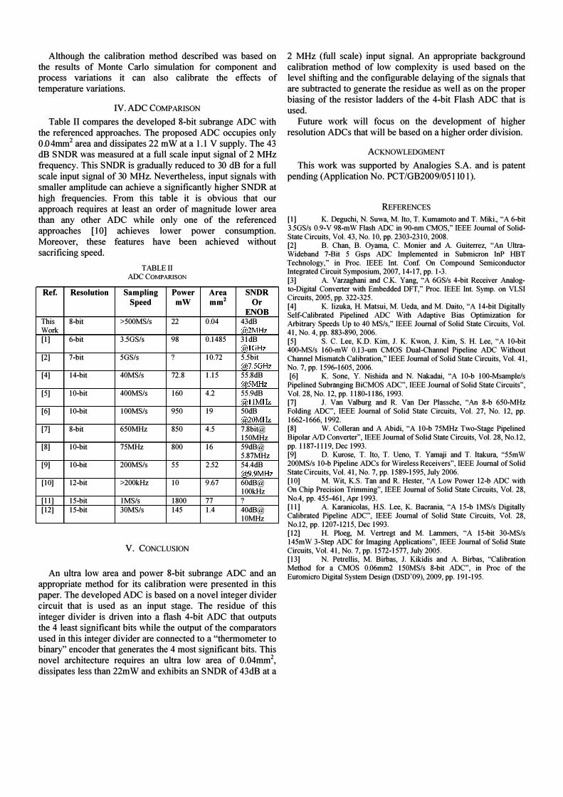
IV. ADC COMPARISON
Table II compares the developed 8-bit subrange ADC with the referenced approaches. The proposed ADC occupies only 0.04mm2 area and dissipates 22 mW at a 1.1 V supply. The 43 dB SNDR was measured at a full scale input signal of 2 MHz frequency. This SNDR is gradually reduced to 30 dB for a full scale input signal of 30 MHz. Nevertheless, input signals with smaller amplitude can achieve a significantly higher SNDR at high frequencies. From this table it is obvious that our approach requires at least an order of magnitude lower area than any other ADC while only one of the referenced approaches [10] achieves lower power consumption. Moreover, these features have been achieved without sacrificing speed.
Ref. Resolution
This 8-bit Work [1] 6-bit
[2] 7-bit
[4] 14-bit
[5] lO-bit
[6] 10-bit
[7] 8-bit
[8] lO-bit
[9] lO-bit
[10] 12-bit
[11] 15-bit [12] 15-bit
TABLE II ADC COMPARISON
Sampling Power Speed mW
>500MS/s 22
3.5GS/s 98
5GS/s ?
40MS/s 72.8
400MS/s 160
100MS/s 950
650MHz 850
75MHz 800
200MS/s 55
>200kHz 10
1 MS/s 1800 30MS/s 145
V. CONCLUSION
Area SNDR mm2 Or
ENOB 0.04 43dB
(aJ2MHz 0.1485 31dB
@IGHz 10.72 5.5bit
(GJ7.5GHz 1.15 55.8dB
(aJ5MHz 4.2 55.9dB
(aJ11MHz 19 50dB
@20MHz 4.5 7.8bit@
150MHz 16 59dB@
5.87MHz 2.52 54.4dB
@9.9MHz 9.67 60dB@
100kHz 77 ? 1.4 40dB@
IOMHz
An ultra low area and power 8-bit subrange ADC and an appropriate method for its calibration were presented in this paper. The developed ADC is based on a novel integer divider circuit that is used as an input stage. The residue of this integer divider is driven into a flash 4-bit ADC that outputs the 4 least significant bits while the output of the comparators used in this integer divider are connected to a "thermometer to binary" encoder that generates the 4 most significant bits. This novel architecture requires an ultra low area of 0.04mm2, dissipates less than 22mW and exhibits an SNDR of 43dB at a
2 MHz (full scale) input signal. An appropriate background calibration method of low complexity is used based on the level shifting and the configurable delaying of the signals that are subtracted to generate the residue as well as on the proper biasing of the resistor ladders of the 4-bit Flash ADC that is used.
Future work will focus on the development of higher resolution ADCs that will be based on a higher order division.
ACKNOWLEDGMENT
This work was supported by Analogies S.A. and is patent pending (Application No. PCT/GB2009/051101).
REFERENCES
[1] K. Deguchi, N. Suwa, M. Ito, T. Kumamoto and T. Miki., "A 6-bit 3.5GS/s 0.9-V 98-mW Flash ADC in 90-nm CMOS," IEEE Journal of SolidState Circuits, Vol. 43, No. 10, pp. 2303-2310, 2008. [2] B. Chan, B. Oyama, C. Monier and A. Guiterrez, "An UltraWideband 7-Bit 5 Gsps ADC Implemented in Submicron InP HBT Technology," in Proc. IEEE Int. Conf. On Compound Semiconductor Integrated Circuit Symposium, 2007, 14-17, pp. 1-3. [3] A. Varzaghani and C.K. Yang, "A 6GS/s 4-bit Receiver Analogto-Digital Converter with Embedded DFT," Proc. IEEE Int. Symp. on VLSI Circuits, 2005, pp. 322-325. [4] K. Iizuka, H. Matsui, M. Ueda, and M. Daito, "A 14-bit Digitally Self-Calibrated Pipelined ADC With Adaptive Bias Optimization for Arbitrary Speeds Up to 40 MS/s," IEEE Journal of Solid State Circuits, Vol. 41, No. 4, pp. 883-890, 2006. [5] S. C. Lee, K.D. Kim, 1. K. Kwon, 1. Kim, S. H. Lee, "A lO-bit 400-MS/s 160-mW 0.13-um CMOS Dual-Channel Pipeline ADC Without Channel Mismatch Calibration," IEEE Journal of Solid State Circuits, Vol. 41, No. 7, pp. 1596-1605, 2006. [6] K. Sone, Y. Nishida and N. Nakadai, "A 10-b 100-Msample/s
Pipelined Subranging BiCMOS ADC", IEEE Journal of Solid State Circuits", Vol. 28, No. 12, pp. 1180-1186, 1993. [7] 1. Van Valburg and R. Van Der Plassche, "An 8-b 650-MHz Folding ADC", IEEE Journal of Solid State Circuits, Vol. 27, No. 12, pp. 1662-1666, 1992. [8] W. Colleran and A Abidi, "A lO-b 75MHz Two-Stage Pipelined Bipolar AID Converter", IEEE Journal of Solid State Circuits, Vol. 28, No.12, pp. 1187-1119, Dec 1993. [9] D. Kurose, T. Ito, T. Ueno, T. Yamaji and T. Itakura, "55mW 200MS/s 10-b Pipeline ADCs for Wireless Receivers", IEEE Journal of Solid State Circuits, Vol. 41, No. 7, pp. 1589-1595, July 2006. [10] M. Wit, K.S. Tan and R. Hester, "A Low Power 12-b ADC with On Chip Precision Trimming", IEEE Journal of Solid State Circuits, Vol. 28, No.4, pp. 455-461, Apr 1993. [11] A. Karanicolas, H.S. Lee, K. Bacrania, "A 15-b IMS/s Digitally Calibrated Pipeline ADC", IEEE Journal of Solid State Circuits, Vol. 28, No.12, pp. 1207-1215, Dec 1993. [12] H. Ploeg, M. Vertregt and M. Lammers, "A 15-bit 30-MS/s 145mW 3-Step ADC for Imaging Applications", IEEE Journal of Solid State Circuits, Vol. 41, No. 7, pp. 1572-1577, July 2005. [13] N. Petrellis, M. Birbas, 1. Kikidis and A. Birbas, "Calibration Method for a CMOS 0.06mm2 150MS/s 8-bit ADC", in Proc of the Euromicro Digital System Design (DSD'09), 2009, pp. 191-195.