Scalable and Systolic Architecture for Computing Double Exponentiation Over GF(2 m
18
Acta Appl Math (2006) 93: 161–178 DOI 10.1007/s10440-006-9071-0 Scalable and Systolic Architecture for Computing Double Exponentiation Over GF(2 m ) Chiou-Yng Lee · Jim-Min Lin · Che Wun Chiou Received: 29 March 2006 / Revised: 29 March 2006 / Accepted: 10 April 2006 / Published online: 22 September 2006 © Springer Science + Business Media B.V. 2006 Abstract Double-exponentiation is a crucial arithmetic operation for many cryp- tographic protocols. Several efficient double-exponentiation algorithms based on systolic architecture have been proposed. However, systolic architectures require large circuit space, thus increasing the cost of the protocol. This would be a drawback when designing circuits in systems requiring low cost and low power consumption. However, some cost savings can be attained by compromising speed, as in portable devices and many embedded systems. This study proposes a scalable and systolic AB 2 and a scalable and systolic A × B, which are the core circuit modules of double- exponentiation. A scalable and systolic double-exponentiation can thus be obtained based on the proposed scalable AB 2 and A × B architecture. Embedded system en- gineers may specify a target double-exponentiation with appropriate scaling systolic circuits. The proposed circuit has lower circuit space/cost and low time/propagation than other circuits. Key words double-exponentiation · Galois field · polynomial basis · systolic architecture · scalable architecture · cryptography. C.-Y. Lee (B ) Department of Computer Information and Network Engineering, Lunghwa University of Science and Technology, Taoyuan County 3306, Taiwan, Republic of China e-mail: [email protected] J.-M. Lin Department of Information Engineering and Computer Science, Feng Chia University, Taichung City 407, Taiwan, Republic of China e-mail: [email protected] C. W. Chiou Department of Computer Science and Information Engineering, Ching Yun University, Chung-Li 320, Taiwan, Republic of China e-mail: [email protected]
Transcript of Scalable and Systolic Architecture for Computing Double Exponentiation Over GF(2 m
Acta Appl Math (2006) 93: 161–178DOI 10.1007/s10440-006-9071-0
Scalable and Systolic Architecture for ComputingDouble Exponentiation Over GF(2m)
Chiou-Yng Lee · Jim-Min Lin · Che Wun Chiou
Received: 29 March 2006 / Revised: 29 March 2006 /Accepted: 10 April 2006 / Published online: 22 September 2006© Springer Science + Business Media B.V. 2006
Abstract Double-exponentiation is a crucial arithmetic operation for many cryp-tographic protocols. Several efficient double-exponentiation algorithms based onsystolic architecture have been proposed. However, systolic architectures requirelarge circuit space, thus increasing the cost of the protocol. This would be a drawbackwhen designing circuits in systems requiring low cost and low power consumption.However, some cost savings can be attained by compromising speed, as in portabledevices and many embedded systems. This study proposes a scalable and systolicAB2 and a scalable and systolic A × B, which are the core circuit modules of double-exponentiation. A scalable and systolic double-exponentiation can thus be obtainedbased on the proposed scalable AB2 and A × B architecture. Embedded system en-gineers may specify a target double-exponentiation with appropriate scaling systoliccircuits. The proposed circuit has lower circuit space/cost and low time/propagationthan other circuits.
Key words double-exponentiation · Galois field · polynomial basis · systolicarchitecture · scalable architecture · cryptography.
C.-Y. Lee (B)Department of Computer Information and Network Engineering,Lunghwa University of Science and Technology, Taoyuan County 3306,Taiwan, Republic of Chinae-mail: [email protected]
J.-M. LinDepartment of Information Engineering and Computer Science,Feng Chia University, Taichung City 407, Taiwan, Republic of Chinae-mail: [email protected]
C. W. ChiouDepartment of Computer Science and Information Engineering,Ching Yun University, Chung-Li 320, Taiwan, Republic of Chinae-mail: [email protected]
162 Acta Appl Math (2006) 93: 161–178
1 Introduction
The power-sum operation (C + AB2) is a significant arithmetic operation for public-key cryptosystems [9] including RSA [32] and Elliptic curve cryptosystem [6], and indecoding multiple-error-correcting binary BCH and RS codes [25, 38, 43]. The AB2
operation is the major portion of this power-sum operation and, thus, is the targetcalculation to be solved in this study.
Finite field (or Galois field) arithmetic operations have been successfully adoptedin solving many complex calculations, such as cryptography [18], switching theory[2], coding theory [19], pseudorandom number generation [36] and digital signalprocessing [5, 29].
Finite field arithmetic operations can be conducted in three different represen-tations, namely normal basis (NB), polynomial basis (PB) and dual basis (DB).The operation performance depends on the representation of the field elements. Asignificant benefit of NB [10, 20, 24, 30, 31, 34, 35, 37] is that it computes the squaringof an element with a cyclic shift of the binary representation. PB [1, 7, 11, 12, 15–17, 21, 22, 26, 27] is extensively adopted, leading to efficient implementation offinite field arithmetic operations. PB has a low design complexity and an extensiblesystem architecture for various applications owing to its greater simplicity, regularityand modularity in architecture than the other two representations. Conversely,the DB representation [3, 44, 45] requires a smaller chip area than the other tworepresentations. This study employs the PB representation.
Although several efficient power-sum architectures [13, 39–41] have been devel-oped with the PB representation of GF(2m), their high space and time complexitiesare major limitations in cryptographic applications. Therefore, further research onefficient power-sum architectures with low space and time complexities is required.This study proposes a scalable and systolic array implementation of the AB2 circuitwith low space complexity by employing circuit folding.
This scalable and systolic AB2 architecture can be adopted to derive several im-portant arithmetic operations, such as the multiplication and double exponentiation.Double-exponentiation is a crucial arithmetic operation for many modern crypto-graphic protocols, such as public-key cryptosystems (Diffie and Hellman [9] andRSA [32]), encoding the Reed Solomon codes [28], and other cryptographic pro-tocols [4, 23, 33]. However, double exponentiation is a rather complicated operation.Therefore, efficient and high-speed double exponentiation algorithms are hard toobtain. Double-exponentiation is traditionally performed by iterating multiplicationoperations. This approach is time-consuming and has high space complexity. Thisstudy therefore aims to solve double-exponentiation using the proposed Galois fieldbased algorithms.
Systolic architecture can lead to cost-effective, high-performance, high throughputspecial-purpose systems for a wide range of problems. In particular, systolic architec-ture has been successfully and widely employed to solve finite field arithmetic opera-tions [8, 13, 16, 17, 21, 22, 36–41] owing to its regularity and ease of reconfiguration. Asystolic array of n array stages can perform up to n multiplications at the same time ina pipelined manner. Systolic architecture has high performance and high throughput,and therefore is appropriate for the applications of high performance server archi-tecture. However, the large scale of systolic circuits makes them expensive. Highperformance and low cost are major concerns in many embedded applications for

Acta Appl Math (2006) 93: 161–178 163
personal use or low system load, while high throughput is unimportant. Therefore, ascalable low-cost systolic architecture that fits to embedded systems is desirable.
This study presents a scalable and systolic architecture for calculating doubleexponentiation in which AB2 represents core scalable and systolic circuits. In theproposed scalable AB2 architecture, a systolic array can be n-folded with the resultproduced by n iterations of the n-folded circuit. Consequently, the circuit space isreduced into 1/n of an original full systolic architecture, while maintaining its originalperformance.
The remainder of this study is structured as follows. Section 2 briefly reviewsthe mathematical background. Section 3 then introduces the proposed scalable andsystolic power-sum circuit based on n-folding. Next, Section 4 presents a multipli-cation circuit based on the proposed scalable and systolic power-sum circuit. Thenovel double exponentiation circuit, which is based on the proposed power-sum andmultiplication in Sections 3 and 4, is then discussed in Section 5. Conclusions arefinally drawn in Section 6.
2 Mathematical Background
The Galois field calculation is the key mathematical foundation of this study. Thisstudy assumes that the readers already have basic knowledge of the Galois fieldoperations, which are described in detail by Lidl and Niederreiter [18]. This sectionreviews some fundamental mathematical results in the Galois field.
Let GF(2m) be a finite field of 2m elements. GF(2m) is an extension field of theground field GF(2). It is an extension field of GF(2), which has elements 0 and 1.All finite fields contain a zero element, a unit element, a primitive element have atleast one primitive irreducible polynomial P(x) = p0 + p1x + · · · + pm−1xm−1 + xm
of degree m over GF(2) associate with it. The primitive element is a root of primitivepolynomial P(x). The non-zero elements of GF(2m) can be represented as powerof the primitive element, i.e., GF(2m) = {0, 1, α, α2, · · · , α2m−2}. Since P(α) = 0, thenwe have αm = p0 + p1α + · · · + pm−1α
m−1. Therefore, the elements of GF(2m) canalso be expressed as polynomial of α with a degree less than m by doing a modP(x) computation over GF(2), i.e., GF(2m) = {A|A = a0 + a1α + · · · + am−2α
m−2 +am−1α
m−1, where ai ∈ GF(2), 0 ≤ i ≤ m − 1}. The basis {1, α, α2, · · · , αm−1} is knownas standard basis and often referred to as polynomial basis, conventional basis orcanonical basis.
In the following, we now briefly describe the multiplication over GF(2m) usingthe canonical basis. Let P(x) be the primitive irreducible polynomial of degree m
for GF(2m) and let α be a root of P(x). Let A =m−1∑
i=0aiα
i and B =m−1∑
i=0b iα
i be two
elements in GF(2m), and let C =m−1∑
i=0ciα
i be the product of A and B. The product C
can be written as follows:
C = ABmodP(x)
= A(b0 + b1α + b2α2 + · · · + bm−1α
m−1)modP(x)
= Ab0modP(x) + Ab1αmodP(x) + · · ·+Abm−1α
m−1modP(x) (1)
164 Acta Appl Math (2006) 93: 161–178
or
C = (· · · (Abm−1modP(x))α + Abm−2modP(x))α
+ · · · )α + Ab0modP(x) (2)
The above equations lead to two types of realizations, least significant bit (LSB)first scheme and most significant bit (MSB) first scheme. LSB and MSB meanthe LSB and MSB of the multiplier B. The LSB first multiplication is based onEquation (1). The intermediate multiplication in the step k, 1 ≤ k ≤ m, does thefollowing computation in parallel.
A(k) = Aαk = (Aαk−1)αmodP(x)
C(k) = C(k−1) + A(k−1)b k−1
where C(0) = 0 and C = AB = C(m). The MSB first multiplication is based onEquation (2). The intermediate multiplication in the step k, 1 ≤ k ≤ m, does thefollowing computation in parallel.
C(k) = C(k−1)α + Abm−kmodP(x) (3)
where C(0) = 0. The essential step in Equation (3) can be identified as follows:
C(k) = c(k)
0 + c(k)
1 α + · · · + c(k)
m−2αm−2 + c(k)
m−1αm−1 (4)
where
c(k)
i = c(k−1)
i−1 + c(k)m−1 pi + aib m−k, for 1 ≤ i ≤ m − 1
c(k)
0 = c(k)
m−1 p0 + a0b m−k (5)
The operations performed in both multiplication algorithms can be identifiedas multiply-by-α, generate-current-products and accumulate-to-previous result. Themultiply-by-α operation is common in both schemes. In the LSB-first scheme, thethree operations are performed in parallel while in the MSB-first scheme they areperformed sequentially. The MSB-first scheme leads to efficient implementationswith a systolic architecture than the LSB-first scheme.
In VLSI designs, systolic architectures are fundamentally suited to rapid compu-tation and depend on regular circuitry to perform arithmetic operations over finitefields GF(2m). Their common nature supports architectural characteristics such asconcurrence, I/O-balance, and simple and regular design. The systolic arrays areone or two-dimensional arrays of simple processing elements that perform specifictask, e.g., matrix–vector multiplication. In the MSB-first scheme, a polynomial basismultiplier using the idea in Equation (5) developed down to the bit-level proved tobe good way to obtain descent designs for VLSI realization of arithmetic processingelements. For an example, Wang–Lin [46] adopts the unidirectional data flowconcept to present a bit-parallel multiplier over GF(2m). The circuit is identical ofm × m cells, each of which consists of two two-input AND gates, one three-inputXOR gates and seven 1-bit latches. The array can provide the maximum throughputof one result per clock cycle after an initial delay of 3m clock periods. The briefpropagation delay of each cell is the total delay of one two-input AND gate, onetwo-input XOR gate and one 1-bit latch.

Acta Appl Math (2006) 93: 161–178 165
3 Proposed Scalable and Systolic AB2 Operation in GF(2m)
AB2 is a conventionally utilized computation in many significant applications,like decoding BCH codes and RS codes, and computing inversions and divisions.Wei–Wei [42] has presented a systolic circuit for AB2 with bidirectional data flowusing a polynomial basis representation of GF(2m). However, this architecture is notappropriate for testable design. Wang and Guo [39] then also utilized a polynomialbasis to show a systolic array for AB2 computation with unidirectional data flowhaving low space complexity, short latency and fault tolerance. Instead of applyingLSB-first schemes in conventional designs, Kim et al. [13] utilized the MSB-firstapproach to further lower the space and time complexities of off-the-shelf AB2
circuits. However, such systolic AB2 architectures have drawbacks such as high spacecomplexity and long latency, still existing when applied to cryptographic application.Hence, this study proposes a novel systolic AB2 architecture adopting the concept offolded computation to reduce the space complexity.
This study develops a scalable and systolic architecture for AB2 in GF(2m). Theterm ‘scalable’ is adopted to describe an architecture of an original m-stages systolicarray performing the AB2 function that can be scaled down in t-stages of a systolicarray ranging from two-folded to at most m-folded. Therefore, such a scaled-downarchitecture is a core and reusable circuit module. The calculation of AB2 of anyword size of bit length m could thus be derived through iteratively operating thisreusable folded circuit module for up to n = �m/t� times. The main benefit ofthis scaled-down architecture is the reduction in cost (due to lower circuit spacerequirement) to approximately 1/n of original circuit.
Assume that a scalable systolic array circuit of t stages is created from two inputdata, A and B, of length m bits, by n iterations, where n = �m/t�.
Let
A = a0 + a1α + · · · + am−1αm−1
B = b0 + b1α + · · · + bm−1αm−1
= b0 + b1α + · · · + bm−1αm−1
+(bmαm + bm+1αm+1 + · · · + bnt−1α
nt−1)
= (b0 + b1α + · · · + bt−1αt−1)
+(btαt + bt+1α
t+1 + · · · + b2t−1α2t−1)
+ · · ·+(b(n−1)tα
(n−1)t + b(n−1)t+1α(n−1)t+1 + · · · + bnt−1α
nt−1)
= (b0 + b1α + · · · + bt−1αt−1)
+(bt + bt+1α + · · · + b2t−1αt−1)αt
+ · · ·+(b(n−1)t + b(n−1)t+1α + · · · + bnt−1α
t−1)α(n−1)t
= B0 + B1αt + · · · + Bn−1α
(n−1)t
where bm = · · · = bnt−1 = 0, Bk = bkt + bkt+1α + · · · + bkt+(t−1)αt−1 and n = �m/t�.

166 Acta Appl Math (2006) 93: 161–178
We are then going to do the computation of AB2:
Y = AB2modP(x)
= A(B0 + B1αt + · · · + Bn−1α
(n−1)t)2modP(x)
= AB20 + AB2
1α2t + · · · + AB2
n−1α2(n−1)tmodP(x)
= (· · · ((0)α2t + AB2n−1)α
2t + AB2n−2)α
2t
+ · · · )α2t + AB20modP(x) (6)
Therefore we can represent the above equation as the form:
Y0 = 0
Yk+1 = Ykα2t + AB2
n−(k+1)
= Ykα2t + A(Bn−(k+1))
2
= Ykα2t + A(b(n−(k+1))t + b(n−(k+1))t+1α
+ · · · + b(n−(k+1))t+(t−1)αt−1)2
= Ykα2t + Ab(n−(k+1))t + Ab(n−(k+1))t+1α
2
+ · · · + Ab(n−(k+1))t+(t−1)α2t−2
= (· · · ((Yk)α2 + Ab (n−(k+1))t+(t−1))α
2
+ · · · )α2 + Ab(n−(k+1))t
AB2 = Yn (7)
where Yk denotes the output of the k-th iteration computation.To compute Equation (7), we may now express it as an iterative form:
Si+1 = Siα2 + Ab(n−(k+1))t+(t−1)−i
= Siα2 + Ab(n−k)t−(i+1) (8)
where 0≤ i ≤ t − 1 and S0 = Yk, Si ∈ GF(2m).
Let Si be represented in polynomial basis, therefore Si is expressed as
Si = si,0 + si,1α + si,2α2 + · · · + si,m−1α
m−1
where si, j ∈ GF(2), 0 ≤ i ≤ t − 1, 0 ≤ j ≤ m − 1. Because α is a root of P(x), thusP(α) = 0 and we have the following results
αm = p0 + p1α + p2α2 + · · · + pm−1α
m−1 (9)
αm+1 = p′0 + p′
1α + p′2α
2 + · · · + p′m−1α
m−1 (10)
where
p′j = pm−1 p j + p j−1 for 1 ≤ j ≤ m − 1
p′0 = pm−1 p0
p0 = 1
Acta Appl Math (2006) 93: 161–178 167
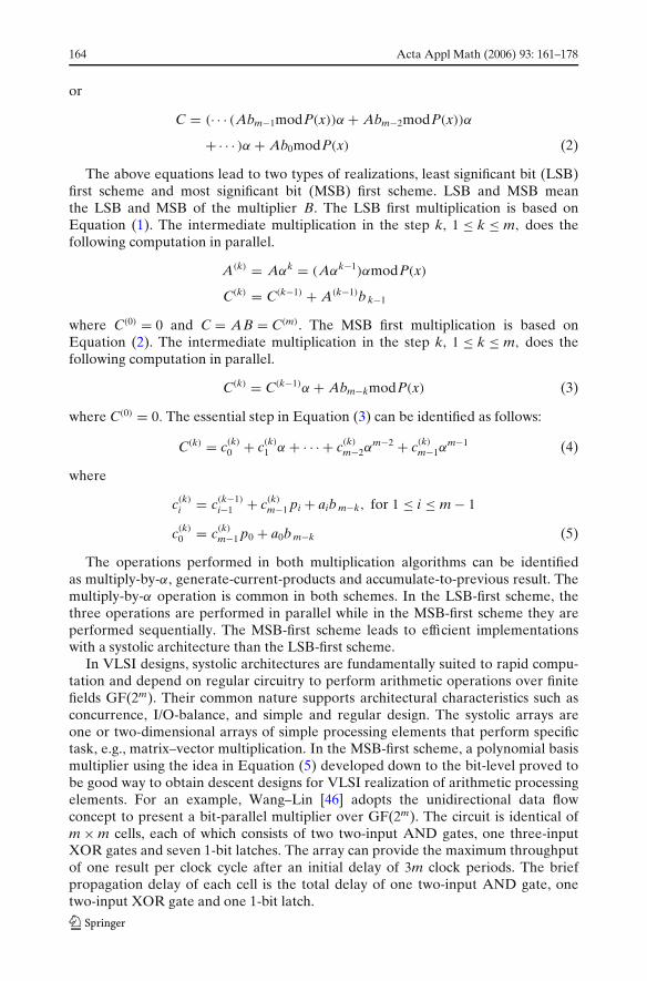
The circuit for computing p′j is shown as Figure 1.
By substituting Equations (9) and (10) into Equation (8), we could extend thisiteration form into the following equation:
Si+1 = Siα2 + Ab(n−k)t−(i+1)
= (si,0 + si,1α + si,2α2 + · · · + si,m−1α
m−1)α2
+(a0 + a1α + a2α2 + · · · + am−1α
m−1)b(n−k)t−(i+1)
= (si,0α2 + si,1α
3 + si,2α4 + · · · + si,m−1α
m+1)
+(a0 + a1α + a2α2 + · · · + am−1α
m−1)b(n−k)t−(i+1)
= si,0α2 + si,1α
3 + si,2α4 + · · · + si,m−3α
m−1
+si,m−2(p0 + p1α + p2α2 + · · · + pm−1α
m−1)
+si,m−1(p′0 + p′
1α + p′2α
2 + · · · + p′m−1α
m−1)
+(a0 + a1α + a2α2 + · · · + am−1α
m−1)b(n−k)t−(i+1)
= (si,m−2 p0 + si,m−1 p′0 + a0b(n−k)t−(i+1))
+(si,m−2 p1 + si,m−1 p′1 + a1b(n−k)t−(i+1))α
+(si,0 + si,m−2 p2 + si,m−1 p′2 + a2b(n−k)t−(i+1))α
2 + · · ·+(si,m−3 + si,m−2 pm−1 + si,m−1 p′
m−1 + am−1b(n−k)t−(i+1))αm−1
= si+1,0 + si+1,1α + si+1,2α2 + · · · + si+1,m−1α
m−1 (11)
Figure 1 Circuit forcomputing P′(x).
p0 p0 p1 p1 p2 pm-2 pm-1 pm-1
p’1 p’2 p’m-1p’0
P
P’

168 Acta Appl Math (2006) 93: 161–178
wheresi+1,0 = si,m−2 p0 + si,m−1 p′
0 + a0b(n−k)t−(i+1)
si+1,1 = si,m−2 p1 + si,m−1 p′1 + a1b(n−k)t−(i+1)
si+1, j = si, j−2 + si, j p j + si, j p′j + a jb(n−k)t−(i+1),
for 2 ≤ j ≤ m − 1 (12)
Based on Equation (12), the scalable and systolic architecture of size t × m forEquation (7) is shown in Figure 2, where there are four input data, namely A, Bk,P and P′. In the circuit, si, j indicates an arbitrary cell. Assume that F is the outputafter each round. F will then be forwarded to an input of next round. After n rounds,the output F will be assigned to the desired result Y. Figure 3 illustrates the blockdiagram of a reusable function module for Y = AB2. This simplified representationis employed for later computations based on AB2. Figure 4 displays the detailedcircuit of the cell S in Figure 2. In round 0 (see Figure 2), the systolic array is used tocalculate F = ABn−1. In round 1, the result F produced in round 0 is forwarded as
Figure 2 The proposed scalable and systolic architecture for Y = AB2.

Acta Appl Math (2006) 93: 161–178 169
Figure 3 Block diagram of areusable function module forY = AB2.
Y
Y=A×B2 mod P
P’
B
PA
the input of the same semi-systolic array to derive the result of the next round. Aftern iterations, the final F is produced as the result of the computation Y.
The number of XOR gates of circuit modules is commonly used as the basisfor comparing their space complexities. This study uses some common assumptionsabout space complexity from Weste and Eshraghian [43]: (1) an XOR gate withthree-input and an XOR gate with four-input are constructed with two two-inputXOR gates and three two-input XOR gates, respectively; (2) a two-input AND gate,a one-bit latch, and a two-input XOR gate consist of six, eight, and six transistors,respectively. The following paragraphs compare the proposed architecture and off-the-shelf AB2 array architectures.
Table 1 lists the results of comparison for various AB2 array architectures. Theproposed single cell S contains 68 transistors. Table 1 indicates that the proposed
Figure 4 Detailed circuit ofan S cell.

170 Acta Appl Math (2006) 93: 161–178
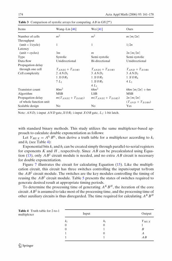
Table 1 Comparison of systolic arrays for computing AB2 in GF(2m)
Items Wang–Guo [39] Wei [40] Wei [41] Ours
Function C + AB2 C + AB2 C + AB2 AB2
Number of cells m2/2 m2 m2 m �m/n�Throughput(unit = 1/cycle) 1 1 1 1/(n)
Latency(unit = cycles) 2.5m 4m m n �m/n�
Type Systolic Systolic Semi-systolic Semi-systolicData flow Unidirectional Bi-directional Bi-directional UnidirectionalPropagation delaythrough one cell TAND2 + TX OR4 TAND + TX OR3 TAND + TX OR3 TAND2 + TX OR4
Cell complexity 6 AND2 3 AND2 3 AND2 3 AND2
2 X OR4 1 X OR2 1 X OR2 1 X OR4
17 L1 1 X OR2 1 X OR3 4 L1
13 L1 4 L1
Transistor count 104m2 140m2 68m2 68m �m/n�Algorithm MSB MSB LSB MSBScalable design No No No Yes
Note: ANDi: i-input AND gate, X ORi: i-input X OR gate, L1: 1-bit latch.
scalable and systolic architecture for the AB2 circuit module can save about (n − 1) ×100/n% in space complexity as compared to other existing AB2 array architectures.For instance, the proposed architecture saves about 50% for n = 2, and 75% for n = 4.
Assume that the propagation delays raised in one cell for all of the listed arrayarchitectures are the same as those in Table 1, since the propagation delays ofgoing through a three-input XOR gate and a four-input XOR gate are the same.Table 1 also reveals that the proposed AB2 array architecture runs as quickly asother existing AB2 array architectures. Additionally, the unidirectional data flow ofthe proposed AB2 array architecture makes the fault-tolerant circuit design easy andpractical.
As for the throughput analysis, previous proposals [39–41] are based on a fullsystolic array with fully pipeline processing for both a single datum and multiple data(the throughput is 1 datum per clock, after the first m clocks latency). By contrast, theproposed architecture is scalable, i.e. a partial systolic array has pipeline processingonly within a single datum and not for contiguous multiple data (throughput is onedatum per �m/n� clocks after the first n �m/n� clocks latency). Restated, the proposalhas the same processing rate as that of a full systolic array for a single datum, but alower throughput for contiguous data. Hence, the proposed scalable architecture isappropriate for an environment requiring fast response and low cost but where onlya few data need to be processed, particularly personal and mobile embedded devices.
Consequently, the proposed AB2 array architecture reusing the folded semi-systolic array has the advantages of saving space complexity and speeding up theexecution time compared with other existing AB2 array architectures.
AB2 is a valuable computation because many operations, such as AB, and AK BH ,can be transformed into computation forms based on AB2. Therefore, the followingsections introduce the calculation of AB and AK BH based on AB2.
Acta Appl Math (2006) 93: 161–178 171
4 The Proposed Multiplication Operation in GF(2m)
This section develops a multiplication operation AB in GF(2m) based on theproposed scalable and systolic AB2. The proposed AB computation is needed tocompute the double exponentiation described later.
Let
A = a0 + a1α + a2α2 + · · · + am−1α
m−1
B = b 0 + b 1α + b 2α2 + · · · + b m−1α
m−1
Then
D = ABmodP(x)
= A(b0 + b1α + b2α2 + · · · + bm−1α
m−1)modP(x)
= A[(b0 + b2α
2 + · · · + bm−2αm−2)
+(b1α + b3α3 + · · · + bm−1α
m−1)]
modP(x)
= A[(b0 + b2α + · · · + bm−2α
m2 −1)2
+α (b1 + b3α + · · · + bm−1αm2 −1)2
]modP(x)
= AB21 + αAB2
2modP(x)
= AB21 + A′ B2
2modP(x) (13)
where
A′ = a0α + a1α2 + a2α
3 + · · · + am−1αmmodP(x)
= a0α + a1α2 + a2α
3 + · · · + am−2αm−1
+am−1(p0 + p1α + p2α2 + · · · + pm−1α
m−1)
= (am−1 p0) + (am−1 p1 + a0)α + · · ·+(am−1 pm−1 + am−2)α
m−1
B1 = b 0 + b 2α + · · · + b m−2αm2 −1
B2 = b 1 + b 3α + · · · + b m−1αm2 −1 (14)
In Equation (14), A′(x) could be obtained through similar circuit of computing P′(x),as shown in Figure 5.
Since AB21 and A′ B2
2 have the same form as the above proposed computationAB2, Equation (13) can be obtained by using twice power-sum iterations. Figure 6depicts the circuit corresponding to Equation (13), which employs switches SW1and SW2 to manage the input pairs A and B1 (for calculating AB2
1) or A′ and B2
(for calculating A′ B22) for two power-sum iterations. Additionally, a switch, SW3,
redirects the result of the first iteration to Y1 linking to a latch buffer, and henceto the result of the second iteration to Y2. Finally, D = AB can thus be obtainedfrom Y1 XOR Y2. Table 2 presents the switch controls to obtain the correct results in

172 Acta Appl Math (2006) 93: 161–178
Figure 5 Detailed circuitof A′.
p0 a0 p1 a1 p2 am-2 pm-1 pm-1
a’1 a’2 a’m-1a’0
A
A’
P
different iterations. Each iteration for generating AB2 takes n′ × t × 1 clock cycles,then AB takes 2n′ × t clock cycles, where n′ = n �m/2t� .
Table 3 compares the proposed and existing multipliers, indicating that theproposed multiplier saves about 75% in space complexity over Wei’s multiplier [41],but has a similar latency. The proposed multiplier also saves about 79% in spacecomplexity over Wang–Lins multiplier [46]. Notably, Wei’s multiplier [41] can beperformed by both functions AB2 + C and AB + C.
5 Proposed Double Exponentiation Operation in GF(2m)
Traditional implementations of double-exponentiation are performed by multi-plying two separate exponentiation computations [14]. For instance, a double-exponentiation AK BH can be performed with two exponentiations, AK and BH ,and one multiplication, AK BH . This study develops a novel approach to performingdouble-exponentiation by iterating of AB2. No additional multiplication circuits areneeded in this approach.
Let
AK = Ak0+k12+···+km−12m−1
BH = Bh0+h12+···+hm−12m−1
Then, the double exponentiation
AK BH = Ak0+k12+···+km−12m−1Bh0+h12+···+hm−12m−1
= (Ak0 Bh0)(Ak1 Bh1)2 · · · (Akm−1 Bhm−1)2m−1
= (· · · ((Akm−1 Bhm−1)2 Akm−2 Bhm−2)2 · · · )2 Ak0 Bh0 (15)

Acta Appl Math (2006) 93: 161–178 173
Figure 6 The circuit forD = AB mod P(x).
SW1
SW2
SW3
Y
Y=IA×IB2
(t×m cells)
P’
IB
PIA
Y1Y2
A’ P’
A P
B
B2
B1
L
D=A×B
Therefore we can represent the above equation as an iterative form:
C0 = 1
Ci = (Akm−i Bhm−i)C2i−1, for 1 ≤ i ≤ m
Finally, after m iterations, we get AK BH = Cm.
Chiou and Lee [8] proposed a multiplexer-based double exponentiation schemethat only requires m multiplications and saves about 66% time complexity compared
Table 2 States for switches inD = AB using AB2 circuitmodule
Iterations of AB2 First iteration Second iteration
SW1 A A′SW2 B1 B2
SW3 Y1 Y2
174 Acta Appl Math (2006) 93: 161–178
Table 3 Comparison of systolic arrays for computing AB in GF(2m)
Items Wang–Lin [46] Wei [41] Ours
Number of cells m2 m2 m �m/2n�Throughput(unit = 1/cycle) 1 1 1/2n
Latency(unit = cycles) 3m m 2n �m/2n�
Type Systolic Semi-systolic Semi-systolicData flow Unidirectional Bi-directional UnidirectionalPropagation delaythrough one cell TAND2 + TX OR3 TAND2 + TX OR3 TAND + TX OR4
Cell complexity 2 AND2 3 AND2 3 AND2
1 X OR3 1 X OR2 1 X OR4
7 L1 1 X OR3 4 L1
4 L1
Transistor count 80m2 68m2 68m �m/2n� + 6mAlgorithm MSB LSB MSBPropagation delay m(TAND2 + TX OR3) m(TAND2 + TX OR3) 2n �m/2n�of whole function unit (TAND + TX OR4)
Scalable design No No Yes
Note: ANDi: i-input AND gate,X ORi: i-input X OR gate, L1: 1-bit latch.
with standard binary methods. This study utilizes the same multiplexer-based ap-proach to calculate double exponentiation as follows:
Let YMU X = Aki Bhi , then derive a truth table for a multiplexer according to ki
and hi (see Table 4):Exponential bits ki and hi can be created simply through parallel-to-serial registers
for exponents K and H , respectively. Since AB can be precalculated using Equa-tion (13), only AB2 circuit module is needed, and no extra AB circuit is necessaryfor double exponentiation.
Figure 7 illustrates the circuit for calculating Equation (15). Like the multipli-cation circuit, this circuit has three switches controlling the inputs/output to/fromthe AB2 circuit module. The switches are the key modules controlling the timing ofreusing the AB2 circuit module. Table 5 presents the states of switches required togenerate desired result at appropriate timing periods.
To determine the processing time of generating AK BH , the iteration of the corecircuit AB2 is assumed to take most of the processing time, and the processing time ofother auxiliary circuits is thus disregarded. The time required for calculating AK BH
Table 4 Truth table for 2-to-1multiplexer Input Output
ki hi YMU X
0 0 10 1 B1 0 A1 1 AB

Acta Appl Math (2006) 93: 161–178 175
Figure 7 The circuit forAK BH mod P(x).
B2
C
1
ki
hi
PTS
K H
SW1
SW2
SW3
YMUX
PTS
Y1 Y2
Z=AKBH
A’ P’
P
B1
L
Y
4 to 1 MUX
1
A B
D
Y=IA×IB2
(t×m cells)
D=A×B
mostly includes the iterations of AB2 for precomputing D = AB and the iterationsof AB2 for generating AK BH . The calculation of D = AB takes two AB2 iterations,that is 2nt clock cycles, and the multiplexer-based AK BH computation takes m times
Table 5 States for switches in Z = AK BH using AB2 circuit module
Iterations of First Second Third Fourth iteration to (m + 2)’thAB2 iteration iteration iteration (m + 1)’th iteration iteration
SW1 A A′ YMU X YMU X YMU X
SW2 B1 B2 1 C CSW3 Y1 Y2 C C Z

176 Acta Appl Math (2006) 93: 161–178
Table 6 Comparison of systolic arrays for computing AK BH modP(x) in GF(2m)
Items Using Wang–Guo Using Wei Using Wei Ours[39] [40] [41]
Number of cells m2/2 m2 m2 m�m/n�Throughput(unit = 1/cycle) 1/2m 1/2m 1/2m 1/(mn)
Latency(unit = cycles) 5m(m − 1) 8m(m − 1) 2m(m − 1) (m + 2)n �m/n�
Type Systolic Systolic Semi-systolic Semi-systolicData flow Unidirectional Bi-directional Bi-directional UnidirectionalPropagation delaythrough one cell TAND2 + TX OR4 TAND + TX OR3 TAND + TX OR3 TAND2 +TX OR4
Cell complexity 6 AND2 3 AND2 3 AND2 3 AND2
2 X OR4 1 X OR2 1 X OR2 1 X OR4
17 L1 1 X OR3 1 X OR3 4 L1
13 L1 4 L1
Transistor count 104m2 140m2 68m2 68m �m/n�Algorithm MSB MSB LSB MSBScalable design No No No Yes
Note: ANDi: i-input AND gate,X ORi : i-input X OR gate, L1: 1-bit latch.
of AB2 iterations, that is mt clock cycles. Therefore, the approximate total processingtime needed to generate AK BH takes (m + 2)nt clock cycles.
Table 6 compares the proposed and traditional double exponentiation archi-tectures. The proposed double exponentiation architecture saves not only spacecomplexity but also time complexity over the traditional double exponentiationarchitecture. For example, the proposed architecture saves about 50%(75%) spacecomplexity and 50%(50%) time complexity for n = 2(n = 4).
6 Conclusions
This study develops a novel double exponentiation architecture with low spacecomplexity based on a core scalable and systolic AB2 circuit. Compared withexisting architectures, the proposed architecture can save at least 50% of space com-plexity (cost) while maintaining approximate single data processing performance.Furthermore, the proposed architecture also saves about 50% time complexity overtraditional architectures. The proposed architecture can be tailored to the desirablescale, and applied to many embedded devices in which space complexity featureis a major design concerns. Further applications of the proposed core scalable andsystolic AB2 circuit could be explored in future works.
Acknowledgement The authors would like to thank the National Science Council of the Republicof China, Taiwan for financially supporting this research under Contract No. NSC94-2213-E-231-021and NSC94-2218-E-262-003.
Acta Appl Math (2006) 93: 161–178 177
References
1. Bartee, T.C., Schneider, D.J.: Computation with finite fields. Inform. and Comput. 6, 79–98(1963)
2. Benjauthrit, B., Reed, I.S.: Galois switching functions and their applications. IEEE Trans. Com-put. C-25, 78–86 (1976)
3. Berlekamp, E.R.: Bit-serial Reed–Solomon encoders. IEEE Trans. Inform. Theory IT-28, 869–874 (1982)
4. Birickell, E.F., McCurley, K.S.: Interactive identification and digital signatures. ATT Tech. J.73–86 (1991)
5. Blahut, R.E.: Fast Algorithms for Digital Signal Processing. Addison-Wesley, Reading,Massachusetts (1985)
6. Blake I., Seroussi, G., Smart, N.: Elliptic Curves in Cryptography. Cambridge University Press,New York (1999)
7. Chiou, C.W., Lin, L.C., Chou, F.H., Shu, S.F.: Low complexity finite field multiplier usingirreducible trinomials. Electron. Lett. 39(24), 1709–1711 (2003)
8. Chiou, C.W., Lee, C.-Y.: Multiplexer-based double-exponentiation for normal basis of GF(2m).Comput. Secur. 24(1), 83–86 (2005)
9. Diffe, W., Hellman, M.E.: New directions in cryptography. IEEE Trans. Inform. Theory 22(6),644–654 (1976)
10. Fan, H., Dai, Y.: Key function of normal basis multipliers in GF(2n). Electron. Lett. 38(23),1431–1432 (2002)
11. Hasan, M.A., Wang, M., Bhargava, V.K.: Modular construction of low complexity parallel mul-tipliers for a class of finite fields GF(2m). IEEE Trans. Comput. 41(8), 962–971 (1992)
12. Itoh, T., Tsujii, S.: Structure of parallel multipliers for a class of fields GF(2m). Inform. andComput. 83, 21–40 (1989)
13. Kim, N.-Y., Kim, H.-S., Yoo, K.-Y.: Computation of AB2 multiplication in GF(2m) using low-complexity systolic architecture. IEE Proc., Circuits Devices Syst. 150(2), 119–123 (2003)
14. Knuth, D.E.: The art of computer programming. In: Seminumerical algorithms, vol. 2. Addison-Wesley, Reading, Massachusetts (1981)
15. Koc, C.K., Sunar, B.: Low-complexity bit-parallel canonical and normal basis multipliers for aclass of finite fields. IEEE Trans. Comput. 47(3), 353–356 (1998)
16. Lee, C.Y., Lu, E.H., Lee, J.Y.: Bit-parallel systolic multipliers for GF(2m) fields defined by all-one and equally-spaced polynomials. IEEE Trans. Comput. 50(5), 385–393 (2001)
17. Lee, C.Y.: Low complexity bit-parallel systolic multiplier over GF(2m) using irreducible trinomi-als. IEE Proc., Comput. Digit. Tech. 150(1), 39–42 (2003)
18. Lidl, R., Niederreiter, H.: Introduction to Finite Fields and their Applications. Cambridge Uni-versity Press, New York (1994)
19. MacWilliams, F.J., Sloane, N.J.A.: The Theory of Error-Correcting Codes. North Holland,Amsterdam (1977)
20. Massey, J.L., Omura, J.K.: Computational method and apparatus for finite field arithmetic. USPatent 4,587,627, May 1986
21. Mastrovito, E.D.: VLSI architectures for multiplication over finite field GF(2m). In: Mora, T.(ed.) Applied Algebra, Algebraic Algorithms, and Error-Correcting Codes, Proceedings of SixthInternational Conference, AAECC-6, Rome, pp. 297–309 (July 1988)
22. Mastrovito, E.D.: VLSI architectures for computations in Galois fields. PhD thesis, LinkopingUniversity, Department of Electrical Engineering, Linkoping, Sweden (1991)
23. NIST: A proposal federal information processing standard for digital signature standard (DSS).Federal Registration 56, 42980–42982 (1991)
24. Oh, S., Kim, C.H., Lim, J., Cheon, D.H.: Efficient normal basis multipliers in composite fields.IEEE Trans. Comput. 49(10), 1133–1138 (2000)
25. Okano, H., Imai, H.: A construction method of high-speed decoders using ROM’s for Bose–Chaudhuri–Hocquenghem and Reed–Solomon codes. IEEE Trans. Comput. C-36, 1165–1171(1987)
26. Paar, C.: A new architecture for a parallel finite field multiplier with low complexity based oncomposite fields. IEEE Trans. Comput. 45(7), 856–861 (1996)
27. Paar, C., Fleischmann, P., Roelse, P.: Efficient multiplier architectures for Galois Fields GF(24n).IEEE Trans. Comput. 47(2), 162–170 (1998)
178 Acta Appl Math (2006) 93: 161–178
28. Reed, I.S., Solomon, G.: Polynomial codes over certain finite fields. SIAM J. Appl. Math. 8, 300–304 (1960)
29. Reed, I.S., Truong, T.K.: The use of finite fields to compute convolutions. IEEE Trans. Inform.Theory IT-21(2), 208–213 (1975)
30. Reyhani-Masoleh, A., Hasoan, M.A.: A new construction of Massey–Omura parallel multiplierover GF(2m). IEEE Trans. Comput. 51(5), 511–520 (2002)
31. Reyhani-Masoleh, A., Hasan, M.A.: Fast normal basis multiplication using general purposeprocessors. IEEE Trans. Comput. 52(11), 1379–1390 (2003)
32. Rivest, R.L., Shamir, A., Adleman, L.: A method for obtaining digital signatures and public-keycryptosystems. Commun. ACM 21(2), 120–126 (1978)
33. Schnorr, C.P.: Efficient identification and signature for smart cards. In: Advances in Cryptology.Crypto’89, Lecture Notes in Computer Science, vol. 435, pp. 239–252. Springer, Berlin Heidel-berg New York (1990)
34. Sunar, B., Koc, C.K.: An efficient optimal normal basis type II multiplier. IEEE Trans. Comput.50(1), 83–87 (2001)
35. Takagi, N., Yoshiki, J.-I., Takagi, K.: A fast algorithm for multiplicative inversion in GF(2m)using normal basis. IEEE Trans. Comput. 50(5), 394–398 (2001)
36. Wang, C.C., Pei, D.: A VLSI design for computing exponentiation in GF(2m) and its applicationto generate pseudorandom number sequences. IEEE Trans. Comput. 39(2), 258–262 (1990)
37. Wang, C.C., Truong, T.K., Shao, H.M., Deutsch, L.J., Omura, J.K., Reed, I.S.: VLSI architecturesfor computing multiplications and inverses in GF(2m). IEEE Trans. Comput. C-34(8), 709–717(1985)
38. Wang, C.-L., Bair, W.-J.: A VLSI architecture for implementation of the decoder for binary BCHcodes. In: Proceedings of Symposium on Communication, Taiwan, pp. 36–40 (Dec 1991)
39. Wang, C.-L., Guo, J.-H.: New systolic arrays for C + AB2, inversion, and division in GF(2m).IEEE Trans. Comput. 49(10), 1120–1125 (2000)
40. Wei, S.-W.: A systolic power-sum circuit for GF(2m ). IEEE Trans. Comput. 43(2), 226–229(1994)
41. Wei, S.-W.: VLSI architectures for computing exponentiations, multiplicative inverses, and divi-sions in GF(2m). IEEE Trans. Circuits Systems I Fund. Theory Appl. 44, 847–855 (1997)
42. Wei, S.-W., Wei, C.H.: High speed decoder of Reed–Solomon codes. IEEE Trans. Commun.41(11), 1588–1593 (1993)
43. Weste N., Eshraghian, K.: Principles of CMOS VLSI Design: A System Perspective. Addison-Wesley, Reading, Massachusetts (1985)
44. Wu H., Hasan, M.A.: Low complexity bit-parallel multipliers for a class of finite fields. IEEETrans. Comput. 47(8), 883–887 (1998)
45. Wu, H., Hasan, M.A., Blake, I.F.: New low-complexity bit-parallel finite field multipliers usingweakly dual bases. IEEE Trans. Comput. 47(11), 1223–1234 (1998)
46. Wang, C.L., Lin, J.L.: Systolic array implementation of multipliers for GF(2m). IEEE Trans.Circuits Syst. II 38(7), 796–800 (1991)