Review and Analysis of the Radiation-Induced Degradation Observed for the Input Bias Current of...
8
3174 IEEE TRANSACTIONS ON NUCLEAR SCIENCE, VOL. 55, NO. 6, DECEMBER 2008 Review and Analysis of the Radiation-Induced Degradation Observed for the Input Bias Current of Linear Integrated Circuits Laurent Dusseau, Senior Member, IEEE, Muriel Bernard, Member, IEEE, Jérôme Boch, Yago Gonzalez Velo, Nicolas Roche, Eric Lorfèvre, Françoise Bezerra, Philippe Calvel, Ronan Marec, and Frédéric Saigné Abstract—It is shown that the variety of shapes of the input cur- rent versus dose curve observed in several ICs is due to circuit ef- fects, depending on the architecture, the value of the currents and the bias conditions. When stages are cascaded, the degradation of the second stage may add or subtract current to the collector cur- rent of the input transistor. The variations of the collector cur- rents can be evaluated using the variations of the supply current. It is then possible to model the compensation effects using basic equations and study the impact of irradiation conditions. In some cases, the effect of biasing the circuit during irradiation is to re- duce the compensation mechanism leading to an stronger increase in the input current. When a peak shaped degradation curve is recorded, annealing may either induce an additional degradation or a recovery depending on which side of the peak irradiation has brought the circuit. Index Terms—Annealing, bipolar transistors, circuit effects, dose rate, integrated circuits (ICs), total dose. I. INTRODUCTION B IPOLAR Integrated Circuits (ICs) are known to be more or less sensitive to Total Ionizing Dose (TID) depending on bias conditions and dose rate, especially when Enhanced Low Dose Rate Sensitivity (ELDRS) is observed [1]. Current research focuses on the development of test methods taking into account ELDRS [2] and associated models [3]. In these works, the input bias current is the parameter often used to describe the radiation-induced degradation of the circuit. The curve de- scribing the degradation of the input bias current for one de- vice may exhibit different behaviors depending on irradiation Manuscript received July 07, 2008; revised August 28, 2008 and September 21, 2008. Current version published December 31, 2008. This work was sup- ported by CNES. L. Dusseau, J. Boch, Y. Gonzalez Velo, N. Roche, and F. Saigné are with the Institut d’Electronique du Sud, University Montpellier II, F-34095 Mont- pellier Cedex 05, France (e-mail: [email protected]; boch@ies. univ-montp2.fr; [email protected]; [email protected]; [email protected]). M. Bernard was with the Institut d’Electronique du Sud, University Montpellier II, F-34095 Montpellier Cedex 05, France. She is now with EADS ASTRIUM GmbH Astrium Satelliten, 182 024 Taufkirchen (e-mail: [email protected]). E. Lorfèvre and F. Bezerra are with Centre National d’Etudes Spatiales, 31401 Toulouse cedex 9, France (e-mail: [email protected]; [email protected]). P. Calvel and R. Marec are with Thales Alenia Space, 31000 Toulouse, France (e-mail: [email protected]; [email protected]; [email protected]). Digital Object Identifier 10.1109/TNS.2008.2006835 conditions, like TID, dose rate, and bias. Moreover, annealing performed after irradiation often yields chaotic variations of the input bias current [4]. The primary goal of this paper is first to demonstrate that the peak shaped curves are mainly due to first order circuit effects rather than compensating physical mecha- nisms such as those observe when the effect of interface states balance the effect of the oxide trap charge in MOS devices. Due to circuit effects, switching the dose rate to accelerate the test in the case of ELDRS sensitive devices may have misleading con- sequences. The second goal of this paper is then to define the proper use of switching dose rate experiments. Finally, many questions have been raised concerning the consistency of re- sults obtained after room temperature or elevated temperature annealing. The third goal of this paper is then to demonstrate that the results of annealing depend on the total ionizing dose delivered and all the irradiation conditions, making them nearly impossible to analyze. Previous publications that focused on a given IC made it possible to better understand the mechanisms responsible for the TID-induced degradation at the circuit level. Barnaby et al. have studied circuit effects in the LM111, ad- dressing the compensation mechanisms in the input stage [5]. Adell et al. have studied the LM124 configured as a voltage comparator and illustrated the role played by the current sources in the overall degradation of the circuits [6]. The circuit effects in the LM139 have also been studied by Bernard et al. [7]. Re- cently, Johnston et al. have synthesized the trends observed in the latest generations of fast ICs [8]. The purpose of the present paper is to review, compare and explain the different types of degradation curves obtained when irradiating widely used ICs such as LM139, LM124 and LM111 in different conditions. The LM101, although obsolete, is also of interest, since its input stage differs significantly from the previously quoted devices. This paper is a sequel to a previous work published in 2004 by Boch et al. [4]. The device used in the present work (with an old date code) as well as the dose rate chosen for the experiments (10 rad(Si)/s were chosen to allow comparison with the data of [4] for which no satisfying explanation had been proposed. Let’s note that National Semiconductor is now manufacturing ELDRS free devices, but older date codes of Commercial Off The Shelf (COTS) devices are still widely being used in many applications. In Section II, a compendium of the types of degrada- tion curves observed is presented. Section III proposes a case-by-case analysis of the degradation mechanisms at the circuit level. The influence of bias conditions and the impact 0018-9499/$25.00 © 2008 IEEE
-
Upload
independent -
Category
Documents
-
view
0 -
download
0
Transcript of Review and Analysis of the Radiation-Induced Degradation Observed for the Input Bias Current of...
3174 IEEE TRANSACTIONS ON NUCLEAR SCIENCE, VOL. 55, NO. 6, DECEMBER 2008
Review and Analysis of the Radiation-InducedDegradation Observed for the Input Bias
Current of Linear Integrated CircuitsLaurent Dusseau, Senior Member, IEEE, Muriel Bernard, Member, IEEE, Jérôme Boch, Yago Gonzalez Velo,
Nicolas Roche, Eric Lorfèvre, Françoise Bezerra, Philippe Calvel, Ronan Marec, and Frédéric Saigné
Abstract—It is shown that the variety of shapes of the input cur-rent versus dose curve observed in several ICs is due to circuit ef-fects, depending on the architecture, the value of the currents andthe bias conditions. When stages are cascaded, the degradation ofthe second stage may add or subtract current to the collector cur-rent of the input transistor. The variations of the collector cur-rents can be evaluated using the variations of the supply current.It is then possible to model the compensation effects using basicequations and study the impact of irradiation conditions. In somecases, the effect of biasing the circuit during irradiation is to re-duce the compensation mechanism leading to an stronger increasein the input current. When a peak shaped degradation curve isrecorded, annealing may either induce an additional degradationor a recovery depending on which side of the peak irradiation hasbrought the circuit.
Index Terms—Annealing, bipolar transistors, circuit effects,dose rate, integrated circuits (ICs), total dose.
I. INTRODUCTION
B IPOLAR Integrated Circuits (ICs) are known to be moreor less sensitive to Total Ionizing Dose (TID) depending
on bias conditions and dose rate, especially when EnhancedLow Dose Rate Sensitivity (ELDRS) is observed [1]. Currentresearch focuses on the development of test methods taking intoaccount ELDRS [2] and associated models [3]. In these works,the input bias current is the parameter often used to describethe radiation-induced degradation of the circuit. The curve de-scribing the degradation of the input bias current for one de-vice may exhibit different behaviors depending on irradiation
Manuscript received July 07, 2008; revised August 28, 2008 and September21, 2008. Current version published December 31, 2008. This work was sup-ported by CNES.
L. Dusseau, J. Boch, Y. Gonzalez Velo, N. Roche, and F. Saigné are withthe Institut d’Electronique du Sud, University Montpellier II, F-34095 Mont-pellier Cedex 05, France (e-mail: [email protected]; [email protected]; [email protected]; [email protected];[email protected]).
M. Bernard was with the Institut d’Electronique du Sud, UniversityMontpellier II, F-34095 Montpellier Cedex 05, France. She is now withEADS ASTRIUM GmbH Astrium Satelliten, 182 024 Taufkirchen (e-mail:[email protected]).
E. Lorfèvre and F. Bezerra are with Centre National d’Etudes Spatiales,31401 Toulouse cedex 9, France (e-mail: [email protected]; [email protected]).
P. Calvel and R. Marec are with Thales Alenia Space, 31000 Toulouse, France(e-mail: [email protected]; [email protected];[email protected]).
Digital Object Identifier 10.1109/TNS.2008.2006835
conditions, like TID, dose rate, and bias. Moreover, annealingperformed after irradiation often yields chaotic variations of theinput bias current [4]. The primary goal of this paper is first todemonstrate that the peak shaped curves are mainly due to firstorder circuit effects rather than compensating physical mecha-nisms such as those observe when the effect of interface statesbalance the effect of the oxide trap charge in MOS devices. Dueto circuit effects, switching the dose rate to accelerate the test inthe case of ELDRS sensitive devices may have misleading con-sequences. The second goal of this paper is then to define theproper use of switching dose rate experiments. Finally, manyquestions have been raised concerning the consistency of re-sults obtained after room temperature or elevated temperatureannealing. The third goal of this paper is then to demonstratethat the results of annealing depend on the total ionizing dosedelivered and all the irradiation conditions, making them nearlyimpossible to analyze. Previous publications that focused on agiven IC made it possible to better understand the mechanismsresponsible for the TID-induced degradation at the circuit level.Barnaby et al. have studied circuit effects in the LM111, ad-dressing the compensation mechanisms in the input stage [5].Adell et al. have studied the LM124 configured as a voltagecomparator and illustrated the role played by the current sourcesin the overall degradation of the circuits [6]. The circuit effectsin the LM139 have also been studied by Bernard et al. [7]. Re-cently, Johnston et al. have synthesized the trends observed inthe latest generations of fast ICs [8]. The purpose of the presentpaper is to review, compare and explain the different types ofdegradation curves obtained when irradiating widely used ICssuch as LM139, LM124 and LM111 in different conditions. TheLM101, although obsolete, is also of interest, since its inputstage differs significantly from the previously quoted devices.This paper is a sequel to a previous work published in 2004 byBoch et al. [4]. The device used in the present work (with an olddate code) as well as the dose rate chosen for the experiments(10 rad(Si)/s were chosen to allow comparison with the dataof [4] for which no satisfying explanation had been proposed.Let’s note that National Semiconductor is now manufacturingELDRS free devices, but older date codes of Commercial OffThe Shelf (COTS) devices are still widely being used in manyapplications.
In Section II, a compendium of the types of degrada-tion curves observed is presented. Section III proposes acase-by-case analysis of the degradation mechanisms at thecircuit level. The influence of bias conditions and the impact
0018-9499/$25.00 © 2008 IEEE

DUSSEAU et al.: REVIEW AND ANALYSIS OF THE RADIATION-INDUCED DEGRADATION 3175
Fig. 1. Input bias current degradation as a function of dose of a LM111 irradi-ated with all pins grounded. Dose rate is 10.8 rad(Si)/s.
Fig. 2. Input bias current degradation as a function of dose for a LM124 irra-diated with all pins grounded. Dose rate is 10.8 rad(Si)/s.
of annealing are also discussed. At this stage, the seeminglychaotic results from [4] are explained as a direct consequenceof the compensation mechanisms at play. In order to allowcomparison, the irradiations are performed on devices of thesame date code as those used in [4] and with the same doserate. Finally, the impact of the shape of the degradation curve isdescribed with respect to the hardness assurance procedure.
II. REVIEW OF EXPERIMENTAL RESULTS
In order to illustrate the different TID induced degradationcurves that may be observed for bipolar ICs, irradiations wereperformed at ONERA DESP (France) using a source. Thedose rate was 10 rad(Si)/s. The curves in Fig. 1to Fig. 4 presentthe degradation of the input bias current of the LM111, theLM124, the LM139 and the LM101. For each device, three partshave been irradiated.
The curve presented is the mean value of the three parts.While the curves on Fig. 3 (LM139) and Fig. 4 (LM101) ex-hibit monotonic behavior, Fig. 1 (LM111) and Fig. 2 (LM124)exhibit curves with a peak in the degradation. It is worth noting
Fig. 3. Input bias current degradation as a function of dose for a LM139 irra-diated with all pins grounded. Dose rate is 10.8 rad(Si)/s.
Fig. 4. Input bias current degradation as a function of dose for a LM101 irra-diated with all pins grounded. Dose rate is 10.8 rad(Si)/s.
that the input stage of the obsolete LM101, is based on the archi-tecture of the LM741 [9] that is two symmetrical emitter cou-pled pairs, is very different from the typical PNP input stages ofthe other circuits [9] based on cascades of npn or pnp transistors.The LM124 and the LM139 share the same input stage structure[Fig. 5(a) and 5(b)]. However, they exhibit different degradationcurves. Finally, the LM111 shows a slightly different architec-ture based on the cascade of two differential pairs (Fig. 6). Thesedifferences are analyzed in Section III.
III. ANALYSIS AT CIRCUIT LEVEL
In the following section, it is understood that TID affects thecarrier recombination in the base of bipolar junction transistors.The increase in surface recombination velocity due to interfacetraps results in an increase in excess base current while the col-lector current is hardly affected [10]. Therefore it is understoodthat the current gain of the transistor decreases. In an analog IC,the emitter current of a transistor is often forced with a currentsource, usually a current mirror. In this case, a drop in the cur-rent gain will lead to an increase of the base current.
As shown in Figs. 5 to 7, input stages are complex assembliesof bipolar transistors that will degrade with dose. Therefore, theinput bias current of the circuit can no longer be considered as
3176 IEEE TRANSACTIONS ON NUCLEAR SCIENCE, VOL. 55, NO. 6, DECEMBER 2008
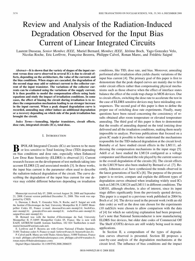
Fig. 5. LM124 and LM139 share a similar input architecture [11], [12], how-ever the values of the current sources are different.
Fig. 6. Simplified schematic of a branch of the LM111 input stage after [13].
Fig. 7. Simplified schematic of the LM101 input stage after [14].
the degradation of a single transistor but rather as the superpo-sition of several degradations.
A. LM124 and LM139
Fig. 5 presents a schematic of the input architecture commonto the LM124 and LM139. Each branch of the differential pairis composed of two substrate (SPNP) transistors [11], [12]. Therole of Q1 in emitter follower configuration as represented inFig. 5 is to increase the input resistance of the circuit. Q1 isbiased with a current mirror.
In the LM139 and LM124, radiation will affect Q1, Q2 andthe current source labeled in Fig. 5 [6]. Let us first con-sider the LM124. Due to the low value of the source biasingQ2 it is reasonable to consider that, even after
a strong degradation, the base current of Q2 is negligible com-pared to the current in the range biasing the emitter of Q1.Two mechanisms are then to be considered: (1) The degradationof Q1 will increase the base current ; (2) the degradation ofthe current source will tend to reduce the emitter current ofQ1 and therefore reduce its base current . The degradation ofthe current sources has been extensively studied and explainedin [6] and confirmed in [7]. These mechanisms will compen-sate each other. The latter becoming prevalent at high doses willproduce the peak shaped degradation observed on the curve ofFig. 1 for devices irradiated with all pins grounded.
Let us now consider the case of the LM139. Although the ar-chitecture is similar, the peak-shaped degradation curve is notobserved. , the current source biasing Q2 is 100 and thecurrent source biasing Q1 is 3.5 . In this case, the contribu-tion of the base current of Q2 to the emitter current of Q1 is inthe range and may increase up to a few tens of since thecurrent gain of Q2 may be divided by a factor of 100 or moreafter irradiation [5]. At the same time, the current source biasingQ1 will degrade and its contribution will become negligible. Asa consequence, it can be assumed that after the first steps of ir-radiation, the emitter current of Q1 is mainly the base currentof Q2. Here, the degradation expected is the cumulative degra-dation of Q1 and Q2. It is worth noting that, from a functionalpoint of view, the increase in the base current of Q2 prevents thecircuit from failing.
Second order mechanisms may be observed in both circuitsif the current source biasing Q2 degrades. In the case of theLM124, reducing the collector current of Q2 contributes to re-ducing the compensation mechanism which explains why theinput bias current rises again after 300 krad(Si) on the curve ofFig. 2. In the case of the LM 139, both the degradation of thesupply current and the degradation of the transistors current gainsaturate, hence the flat response observed at high doses.
B. LM111
The circuit effects in the LM111 have been studied byBarnaby et al. [5]. Like the LM124, the LM111 exhibits anon monotonic peak-shaped degradation curve. Here, the inputstage is composed of a SPNP transistor in emitter followerconfiguration connected to a NPN differential pair as shownin Fig. 6. The degradation of both Q2 and the current sourcewill combine to reduce the emitter current of Q1, leading tothe strong compensation mechanism observed in the curve ofFig. 3.
C. LM101
The structure of the input stage of the LM101 is presentedin Fig. 7. On each branch, a transistor in emitter follower input(Q1 and Q2) is followed by a common bases stage. From thesmall signal analysis point of view, this structure acts as emittercoupled stage. This stage is biased with a very stable currentsource. Hence, in this specific case, the degradation observedis mainly due to the degradation of the input transistor, withno compensation mechanism possible as found for the curve ofFig. 4.
DUSSEAU et al.: REVIEW AND ANALYSIS OF THE RADIATION-INDUCED DEGRADATION 3177
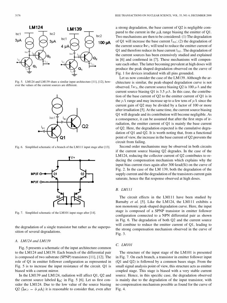
Fig. 8. Experimental (dots) and a fit of the variations of the input bias currentrecorded on a LM124J EH306AB irradiated @ 11 rad(Si)/s.
IV. MODELING AND ANALYSIS
A. Modeling the Compensation Mechanism
Compensation mechanism is observed when two or morecomponents of the structure degrade simultaneously. Bothdegradations may also exhibit saturation at different TID level.In this section, it is shown that the compensation mechanismcan be described using basic equations. Let us consider thesimple case of the LM124 [Fig. 4(a)] and only take into accountthe input transistor and Isc1 as suggested in Section III-A. Inorder to model the compensation phenomenon, the degradationof the input bias current and the degradation of the supplycurrent have to be evaluated; both curves can be measuredexperimentally. Unfortunately, the degradation of the currentgain of the input transistors is not directly accessible and hasto be extracted. The following section proposes a three-stepmodeling process. Once the model is obtained, it is possibleto vary the degradation rates and compare the changes in thecurves with results obtained in other bias configurations.
Step 1: Fit of Input Bias Current and Supply Current: Fig.8. shows experimental data of the variations of the input biascurrent for a LM124 EH306AB with all pins grounded whilebeing irradiated with X-rays at 11 rad(Si)/s.
The solid line on Fig. 8 shows the result of a fit obtained using
(1)
Where, , , and are parameters adjusted numerically andD represents the Total Ionizing Dose. Let us note that this stepis purely mathematical and requires no knowledge about themechanisms at play.
The degradation of the supply current was also recorded andfitted. The equation used for the fit is the typical dependence ofa simple current mirror on the current gain of the constituenttransistors [6], that is
(2)
where is the output current of the mirror, n the number of tran-sistors in the current mirror and the input reference current.
Fig. 9. Experimental data (dots) and fit of the supply current as a function oftotal dose for a LM124J EH306AB irradiated @ 11 rad(Si)/s.
Varying only in (2) leads to a saturation of the degrada-tion. The tail of the experimental degradation curve shows that
also degrades with dose. This additional degradation wasmodeled on the curve of Fig. 9 using a slow exponential decayfunction.
Step 2: Extraction of the Degradation of the Current Gain:It is assumed that the supply current is the sum of all the cur-rents delivered by all the current mirrors in parallel [6]. It is thenreasonable to assume that the degradation of the current sourcebiasing the input stage can be obtained by scaling the curve ofFig. 9 to the 3 delivered by this mirror. It is then possible tocalculate the degradation of the current gain of the input tran-sistor using
(3)
where I+ is the base current of the input transistor, is thecurrent delivered by the current source and is the current gainof the transistor.
Fig. 10 shows a comparison of the current gain versus doseestimated using (2) with the experimental data from Barnaby etal. [5]. Both curves exhibit high degradation rates and a verysimilar shape. Although the dose rate used in [5], [50 rad(Si)/s]is higher than the 11 rad(Si)/s used in this work, both are highenough and the compensation mechanism remains the same.
Step 3: Modeling: At this stage, the degradation of the currentgain and the supply current have been modeled analytically withdata recorded on devices irradiated with all pins grounded. It iseasy to verify that the curve of Fig. 8 can be obtained using
(4)
but the real interest of this model is to make it possible to inves-tigate the behavior of the compensation mechanism when dif-ferent bias conditions are applied during irradiation.
Modeling Effect of Biasing During Irradiation: Duringground level based testing as well as in flight, circuits may beirradiated in different bias configurations. It has been shownthat a 0 V bias on the Base Emitter junction during irradiationwas generally a worst case for the degradation of bipolarjunction transistors [15], [16]. In a circuit, depending on the

3178 IEEE TRANSACTIONS ON NUCLEAR SCIENCE, VOL. 55, NO. 6, DECEMBER 2008
Fig. 10. Degradation of the current gain of the input SPNP transistors estimatedusing (1) and experimental data from [5].
configuration, some transistors may be biased while others willhave a near zero voltage applied on the emitter base junction.This is the case for a circuit irradiated with a supply voltage andone or both of the input pins grounded. Such a bias dependentradiation-induced degradation has already been reported in[7] for the LM139. When the device is irradiated with all pinsgrounded, the degradation of the current mirror biasing theinput transistor is maximized since the emitter-base voltage isequal to 0 V. The stronger the degradation of the current source,the stronger will be the compensation mechanism. When theIC is biased during irradiation, the transistors constituting thecurrent mirror operate with a base emitter voltage close to0.6 V, yielding less degradation of the current sources.
The compensation mechanisms described in Section III hasless impact and the input current keeps increasing at high doses.This effect can be easily be modeled using (4).
The curves in Fig. 11 present experimental data recorded ona LM124 EH306 AB irradiated with all pins grounded (squaresymbols) and at (triangles). Since in both configu-rations the input pins are grounded, it is assumed that the varia-tions of the current gain of the input transistors remain the same(Fig. 10). The solid line was sketched using (4) and the degra-dation of given in Fig. 11. The dashed line was obtained bysimply using the same equation and the supply current of thedevice irradiated under a 5 V bias, scaled to 3 as shown inFig. 10.
The bias-induced reduction of the compensation mechanismwas also observed for the same device but with other date codes(Fig. 13) and other devices (Fig. 14).
B. Interpretation of Post Irradiation Annealing
Many authors have reported a variety of annealing effects onlinear ICs. Boch et al. [4] have shown that the impact of a roomtemperature anneal on the input bias current of the LM124 waseither a recovery or a sudden increase, depending on TID. Thus,the authors have suggested using the sign of the variation in-duced by annealing to detect the saturation region of the degra-dation curve. However, this mechanism was not yet understood.In this section, an explanation based on the compensation mech-anism and the model presented in Section IV-A is proposed.
Fig. 11. Degradation of the input bias current of a LM124 irradiated grounded(square symbols) and biased (triangles). Dose rate is 11 rad(Si)/s. The change inthe shape can be modeled by decreasing the degradation of the supply current.
Fig. 12. Degradation of the supply current of LM 124 irradiated grounded (tri-angles) and biased (square symbols). Dose rate is 11 rad(Si)/s. The change inthe shape can be modeled by decreasing the degradation of the supply current.
Fig. 13. Degradation of the input bias current of a LM 124 irradiated grounded(round symbols) and biased (triangles). Dose rate is 11 rad(Si)/s.
In their work, Boch et al. used a series of alternating irra-diations at 10.8 rad(Si)/s and room temperature anneals on theLM124 [4] and plotted the variations of the input bias currentversus time. Fig. 13 presents the results obtained for the inputbias current and the supply current. In Fig. 15, the regions ingrey correspond to the annealing periods. The regions in whitecorrespond to the irradiation periods. Let us first consider the
DUSSEAU et al.: REVIEW AND ANALYSIS OF THE RADIATION-INDUCED DEGRADATION 3179
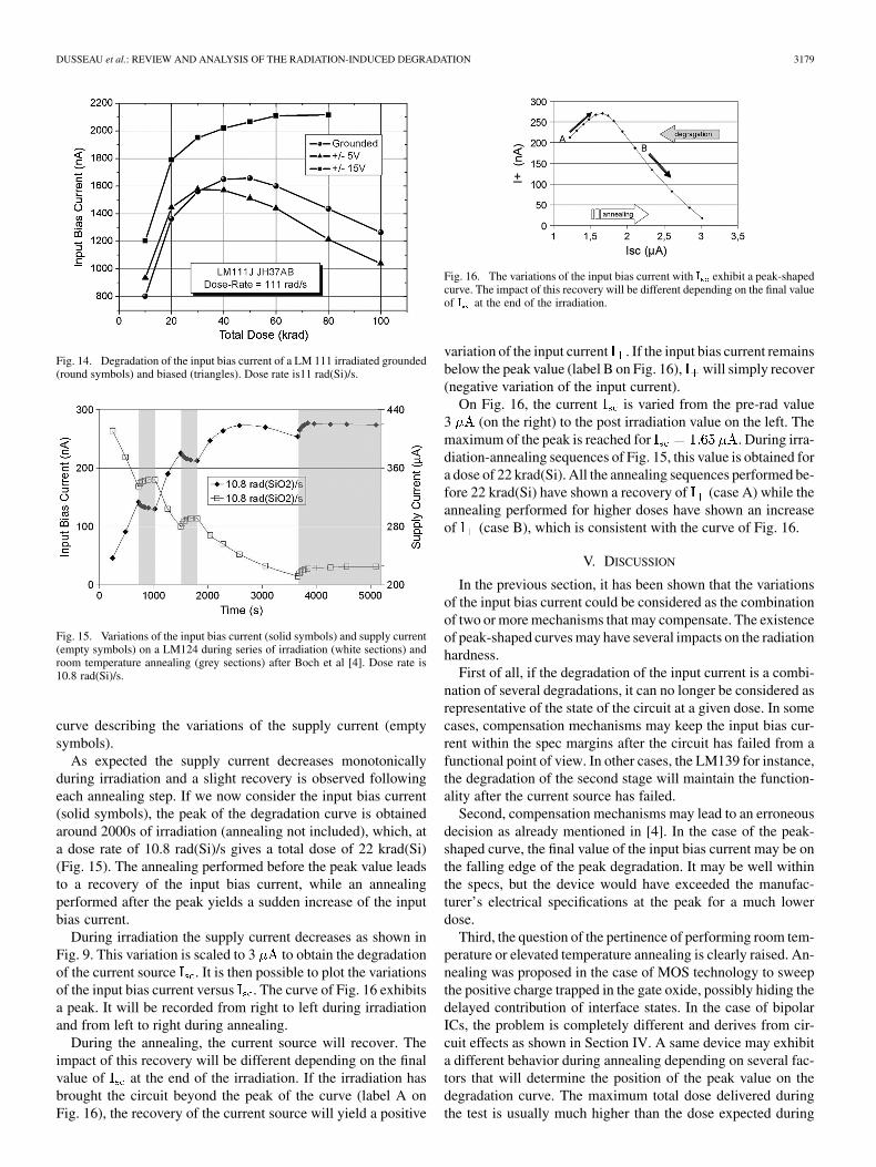
Fig. 14. Degradation of the input bias current of a LM 111 irradiated grounded(round symbols) and biased (triangles). Dose rate is11 rad(Si)/s.
Fig. 15. Variations of the input bias current (solid symbols) and supply current(empty symbols) on a LM124 during series of irradiation (white sections) androom temperature annealing (grey sections) after Boch et al [4]. Dose rate is10.8 rad(Si)/s.
curve describing the variations of the supply current (emptysymbols).
As expected the supply current decreases monotonicallyduring irradiation and a slight recovery is observed followingeach annealing step. If we now consider the input bias current(solid symbols), the peak of the degradation curve is obtainedaround 2000s of irradiation (annealing not included), which, ata dose rate of 10.8 rad(Si)/s gives a total dose of 22 krad(Si)(Fig. 15). The annealing performed before the peak value leadsto a recovery of the input bias current, while an annealingperformed after the peak yields a sudden increase of the inputbias current.
During irradiation the supply current decreases as shown inFig. 9. This variation is scaled to 3 to obtain the degradationof the current source . It is then possible to plot the variationsof the input bias current versus . The curve of Fig. 16 exhibitsa peak. It will be recorded from right to left during irradiationand from left to right during annealing.
During the annealing, the current source will recover. Theimpact of this recovery will be different depending on the finalvalue of at the end of the irradiation. If the irradiation hasbrought the circuit beyond the peak of the curve (label A onFig. 16), the recovery of the current source will yield a positive
Fig. 16. The variations of the input bias current with � exhibit a peak-shapedcurve. The impact of this recovery will be different depending on the final valueof � at the end of the irradiation.
variation of the input current . If the input bias current remainsbelow the peak value (label B on Fig. 16), will simply recover(negative variation of the input current).
On Fig. 16, the current is varied from the pre-rad value3 (on the right) to the post irradiation value on the left. Themaximum of the peak is reached for . During irra-diation-annealing sequences of Fig. 15, this value is obtained fora dose of 22 krad(Si). All the annealing sequences performed be-fore 22 krad(Si) have shown a recovery of (case A) while theannealing performed for higher doses have shown an increaseof (case B), which is consistent with the curve of Fig. 16.
V. DISCUSSION
In the previous section, it has been shown that the variationsof the input bias current could be considered as the combinationof two or more mechanisms that may compensate. The existenceof peak-shaped curves may have several impacts on the radiationhardness.
First of all, if the degradation of the input current is a combi-nation of several degradations, it can no longer be considered asrepresentative of the state of the circuit at a given dose. In somecases, compensation mechanisms may keep the input bias cur-rent within the spec margins after the circuit has failed from afunctional point of view. In other cases, the LM139 for instance,the degradation of the second stage will maintain the function-ality after the current source has failed.
Second, compensation mechanisms may lead to an erroneousdecision as already mentioned in [4]. In the case of the peak-shaped curve, the final value of the input bias current may be onthe falling edge of the peak degradation. It may be well withinthe specs, but the device would have exceeded the manufac-turer’s electrical specifications at the peak for a much lowerdose.
Third, the question of the pertinence of performing room tem-perature or elevated temperature annealing is clearly raised. An-nealing was proposed in the case of MOS technology to sweepthe positive charge trapped in the gate oxide, possibly hiding thedelayed contribution of interface states. In the case of bipolarICs, the problem is completely different and derives from cir-cuit effects as shown in Section IV. A same device may exhibita different behavior during annealing depending on several fac-tors that will determine the position of the peak value on thedegradation curve. The maximum total dose delivered duringthe test is usually much higher than the dose expected during
3180 IEEE TRANSACTIONS ON NUCLEAR SCIENCE, VOL. 55, NO. 6, DECEMBER 2008
Fig. 17. Illustration of the dose rate switching method after Boch et al [2] Anaccurate LDR degradation curve is obtained.
a mission. If the test has brought the device beyond the peakwhich may never happen in flight, the sudden annealing maylead to an increased degradation that is a pure artifact. More-over, dose rate and bias conditions will combine to modify theshape of the degradation curve, shifting the peak or preventingthe compensation mechanisms. In other words, the annealingwill only be meaningful if the device is irradiated in the exactin-flight conditions.
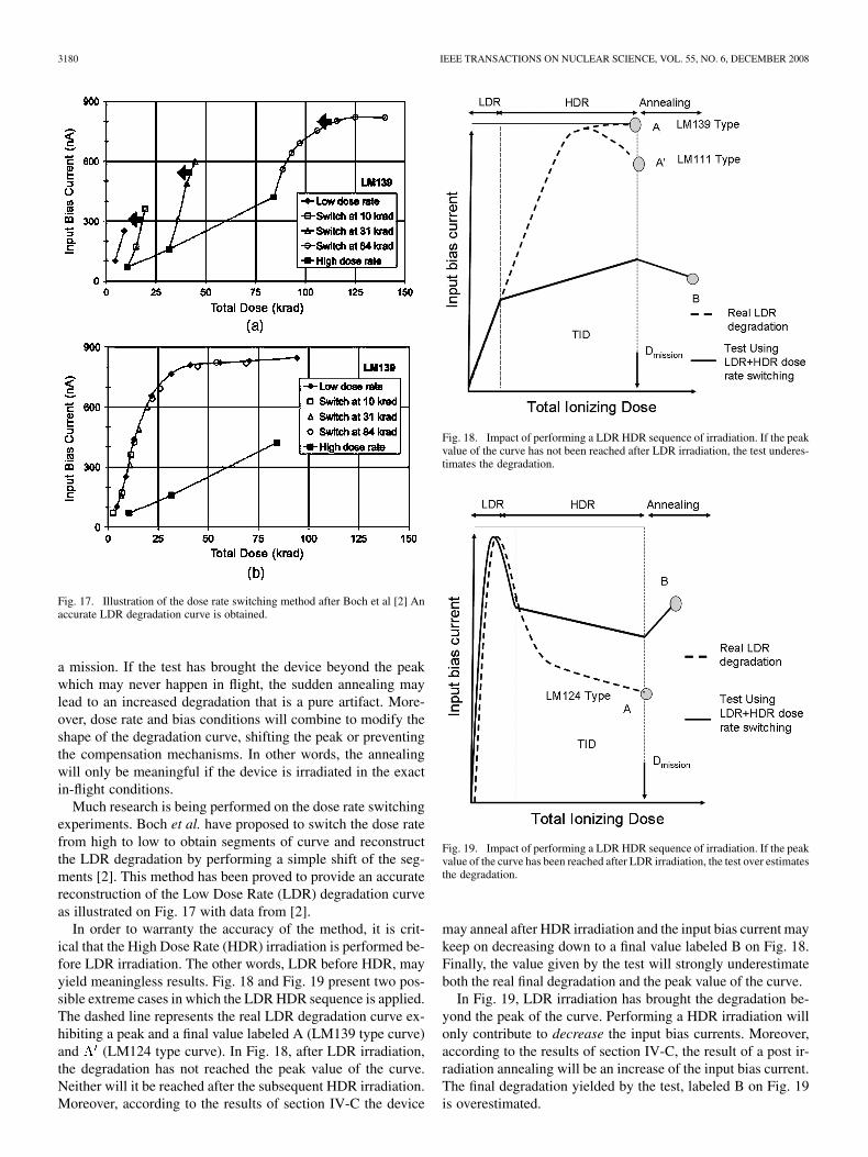
Much research is being performed on the dose rate switchingexperiments. Boch et al. have proposed to switch the dose ratefrom high to low to obtain segments of curve and reconstructthe LDR degradation by performing a simple shift of the seg-ments [2]. This method has been proved to provide an accuratereconstruction of the Low Dose Rate (LDR) degradation curveas illustrated on Fig. 17 with data from [2].
In order to warranty the accuracy of the method, it is crit-ical that the High Dose Rate (HDR) irradiation is performed be-fore LDR irradiation. The other words, LDR before HDR, mayyield meaningless results. Fig. 18 and Fig. 19 present two pos-sible extreme cases in which the LDR HDR sequence is applied.The dashed line represents the real LDR degradation curve ex-hibiting a peak and a final value labeled A (LM139 type curve)and (LM124 type curve). In Fig. 18, after LDR irradiation,the degradation has not reached the peak value of the curve.Neither will it be reached after the subsequent HDR irradiation.Moreover, according to the results of section IV-C the device
Fig. 18. Impact of performing a LDR HDR sequence of irradiation. If the peakvalue of the curve has not been reached after LDR irradiation, the test underes-timates the degradation.
Fig. 19. Impact of performing a LDR HDR sequence of irradiation. If the peakvalue of the curve has been reached after LDR irradiation, the test over estimatesthe degradation.
may anneal after HDR irradiation and the input bias current maykeep on decreasing down to a final value labeled B on Fig. 18.Finally, the value given by the test will strongly underestimateboth the real final degradation and the peak value of the curve.
In Fig. 19, LDR irradiation has brought the degradation be-yond the peak of the curve. Performing a HDR irradiation willonly contribute to decrease the input bias currents. Moreover,according to the results of section IV-C, the result of a post ir-radiation annealing will be an increase of the input bias current.The final degradation yielded by the test, labeled B on Fig. 19is overestimated.
DUSSEAU et al.: REVIEW AND ANALYSIS OF THE RADIATION-INDUCED DEGRADATION 3181
Fig. 18 and Fig. 19 show clearly that, due to compensationmechanisms and peak shaped curves, the same test may providetwo different results, none of which is accurate. The major con-cern is that the dose for which the peak value is reached dependson bias, dose rate, ELDRS sensitivity and circuit architecture.Therefore, the result of LDR HDR sequence of irradiation is al-most impossible to analyze.
VI. CONCLUSION
In this paper it has been shown that the shapes of the inputcurrent versus dose curves observed for four different ICs maybe explained and predicted by means of circuit analysis, con-sidering the sum of currents at critical nodes. On the one hand,two different mechanisms leading to same curve shapes havebeen identified. On the other hand, it has been shown that iden-tical structures might have different behaviors depending on thevalue of the currents involved. A simple equation made it pos-sible to model the peak of the current degradation in the case ofa LM124. This equation shows that a lower degradation of thecurrent source may explain why no compensation mechanismis observed when a supply voltage is applied during irradiation.It was also shown that the results of a post irradiation annealingdepends on the compensation mechanisms.
ACKNOWLEDGMENT
The authors would like to thank the Centre National d’EtudesSpatiales for their long term support on this work.
REFERENCES
[1] R. K. Freitag and D. B. Brown, “Study of low-dose-rate radiation ef-fects on commercial linear bipolar ICs,” IEEE Trans. Nucl. Sci., vol.45, no. 6, pp. 2649–2658, Dec. 1998.
[2] J. Boch, F. Saigné, R. D. Schrimpf, J.-R. Vaillé, L. Dusseau, S. Ducret,M. F. Bernard, E. Lorfevre, and C. Chatry, “Estimation of low doserate degradation on bipolar linear integrated circuits using switch-ingexperiments,” IEEE Trans. Nucl. Sci., vol. 52, no. 6, pp. 2616–2621,Dec. 2005.
[3] J. Boch, F. Saigne, R. D. Schrimpf, J. R. Vaille, L. Dusseau, and E. Lor-fevre, “Physical model for the low-dose-rate effect in bipolar devices,”IEEE Trans. Nucl. Sci., vol. 53, no. 6, pp. 3655–3660, Dec. 2006.
[4] J. Boch, F. Saigne, S. Ducret, R. D. Schrimpf, D. M. Fleetwood, P. Iac-coni, and L. Dusseau, “Total dose effects on bipolar integrated circuits:Characterization of the saturation region,” IEEE Trans. Nucl. Sci., vol.51, no. 6, pp. 3225–3230, Dec. 2004.
[5] H. J. Barnaby, R. D. Schrimpf, R. L. Pease, P. Cole, T. Turflinger,J. Krieg, and J. Titus, “Identification of degradation mechanisms in abipolar linear voltage comparator through correlation of transistor andcircuit response,” IEEE Trans. Nucl. Sci., vol. 46, no. 6, pp. 1666–1673,Dec. 1999.
[6] P. C. Adell, R. D. Schrimpf, W. T. Holman, J. L. Todd, S. Caveriv-iere, R. R. Cizmarik, and K. F. Galloway, “Total dose effects in alinear voltage regulator,” IEEE Trans. Nucl. Sci., vol. 51, no. 6, pp.3816–3821, Dec. 2004.
[7] M. Bernard, L. Dusseau, J. Boch, J. R. Vaille, F. Saigne, R. D.Schrimpf, E. Lorfevre, and J. P. David, “Analysis of bias effectsonthe total-dose response of a bipolar voltage comparator,” IEEE Trans.Nucl. Sci., vol. 53, no. 6, pp. 3232–3236, Dec. 2006.
[8] A. Johnston and B. Rax, “Testing and qualifying linear integrated cir-duits for radiation degradation in space,” IEEE Trans. Nucl. Sci., vol.53, no. 6, pp. 1779–1786, Dec. 2006.
[9] P. R. Gray and R. G. Meyer, Analysis and Design of Analog IntegratedCircuits, 2nd ed. New York: Wiley, 1984.
[10] D. M. Fleetwood, S. L. Kosier, R. N. Nowlin, R. D. Schrimpf, R. A.Reber, Jr., M. DeLaus, P. S. Winokur, A. Wei, W. E. Combs, and R.L. Pease, “Physical mechanisms contributing to enhanced bipolar gaindegradation at low dose rates,” IEEE Trans. Nucl. Sci., vol. 41, no. 6,pp. 1871–1883, Dec. 1994.
[11] National Semiconductor, Santa Clara, CA, “LM124 Datasheet,” 2000.[Online]. Available: http://www.national.com/mpf/LM/LM124.html
[12] National Semiconductor, Santa Clara, CA, “LM139 Datasheet,” 2004.[Online]. Available: http://www.national.com/mpf/LM/LM139.html
[13] National Semiconductor, Santa Clara, CA, “LM111 Datasheet,” 2001.[Online]. Available: http://www.national.com/mpf/LM/LM111.html
[14] National Semiconductor, Santa Clara, CA, “LM101 Datasheet,” 2000.[Online]. Available: http://www.national.com/mpf/LM/LM101.html
[15] H. J. Barnaby, C. Cirba, R. D. Schrimpf, S. Kosier, P. Fouillat, andX. Montagner, “Minimizing gain degradation in lateral PNP bipolarjunction transistors using gate control,” IEEE Trans. Nucl. Sci., vol.46, no. 6, pp. 1652–1659, Dec. 1999.
[16] V. S. Pershenkov, B. V. Tiwari, S. V. Cherepko, I. N. Shvetzov-Shilovsky, V. V. Belyakov, A. V. Sogoyan, V. I. Rusanovsky, V. ,N. Ulimov, V. V. Emelianov, and V. S. Nasibullin, “The effect ofemitter junction bias on the low dose-rate radiation response of bipolardevices,” IEEE Trans. Nucl. Sci., vol. 44, no. 6, pp. 1840–1848, Dec.1997.