Research directions and challenges in nanoelectronics
18
Perspectives Research directions and challenges in nanoelectronics R. K. Cavin 1 , V. V. Zhirnov 1,3, *, D. J. C. Herr 1 , Alba Avila 2 and J. Hutchby 1 1 Semiconductor Research Corporation, Research Triangle Park, Durham, NC, 27709-2053, USA; 2 University of the Andes, Carrera 1 Este N. 18 A 70, Bogota ´, Colombia; 3 Semiconductor Research Corporation, Brighton Hall, Suite 120, 1101 Slater Road, Durham, NC, 27703, USA; *Author for correspondence (Tel.: +1-919-941-9454; Fax: +1-919-941-9450; E-mail: [email protected]) Received 11 April 2006; accepted in revised form 1 May 2006 Key words: binary switch, non-equilibrium systems, interconnect technologies, thermal management, directed self-assembly, industry–government collaboration, nanotechnology Abstract The search for alternate information processing technologies to sustain Moore’s Law improvements beyond those attainable by scaling of charge-based devices encompasses several key technologies. Some of these technologies were explored at the Third Workshop on Silicon Nanoelectronics and Beyond (SNB III) held at the National Science Foundation in Washington DC in December 2005. They included: (1) non- charge-based devices; (2) devices operated out of thermal equilibrium; (3) alternative interconnect systems; (4) thermal extraction limits and technologies; and (5) fabrication via directed self-assembly. Although this paper was inspired by this highly successful workshop, it is not intended as a summary, but rather an assessment by the authors of some of the fundamental physical considerations evident at the present time. Introduction Many research issues pertinent to extending Moore’s law scaling for nanoelectronics are being addressed by the portfolio of the U. S. National Nanotechnology Initiative (NNI). A good over- view of NNI strategic directions along with emphasis planned for fiscal year 2007 can be found in (Roco, 2006). In January 2005, the National Science Foundation (NSF) and the Semiconductor Research Corporation (SRC) signed a Memoran- dum of Understanding authorizing the conduct of joint programs in the domain of nanoelectronics. The joint NSF/SRC ‘‘Silicon Nanoelectronics and Beyond Program’’ provides mechanisms for involving industry in NNI research in nanoelec- tronics. Another example of industry collabora- tion with NSF is the joint Industry/NSF supplemental funding for six NSF centres focused on discovery of the next switch beyond CMOS. There remain many formidable challenges to developing technologies for charge-based devices whose performance approaches the best theoreti- cally achievable. For example, the energy con- sumed per operation by current generation devices is on the order of 10 4 to 10 6 of that which is set by fundamental physics. A broad spectrum of research and development is needed in the under- lying disciplines if we are to even approach the physical limits and this will probably include new material systems, new fabrication processes, and new device and interconnect structures. The 2005 edition of the International Technology Roadmap for Semiconductors provides a detailed analysis of technology needs and is a rich resource for research opportunities. It is likely that one-to-two more Journal of Nanoparticle Research (2006) 8:841–858 Ó Springer 2006 DOI 10.1007/s11051-006-9123-4
-
Upload
independent -
Category
Documents
-
view
0 -
download
0
Transcript of Research directions and challenges in nanoelectronics

Perspectives
Research directions and challenges in nanoelectronics
R. K. Cavin1, V. V. Zhirnov1,3,*, D. J. C. Herr1, Alba Avila2 and J. Hutchby11Semiconductor Research Corporation, Research Triangle Park, Durham, NC, 27709-2053, USA; 2Universityof the Andes, Carrera 1 Este N. 18 A 70, Bogota, Colombia; 3Semiconductor Research Corporation, BrightonHall, Suite 120, 1101 Slater Road, Durham, NC, 27703, USA; *Author for correspondence(Tel.: +1-919-941-9454; Fax: +1-919-941-9450; E-mail: [email protected])
Received 11 April 2006; accepted in revised form 1 May 2006
Key words: binary switch, non-equilibrium systems, interconnect technologies, thermal management,directed self-assembly, industry–government collaboration, nanotechnology
Abstract
The search for alternate information processing technologies to sustain Moore’s Law improvementsbeyond those attainable by scaling of charge-based devices encompasses several key technologies. Some ofthese technologies were explored at the Third Workshop on Silicon Nanoelectronics and Beyond (SNB III)held at the National Science Foundation in Washington DC in December 2005. They included: (1) non-charge-based devices; (2) devices operated out of thermal equilibrium; (3) alternative interconnect systems;(4) thermal extraction limits and technologies; and (5) fabrication via directed self-assembly. Although thispaper was inspired by this highly successful workshop, it is not intended as a summary, but rather anassessment by the authors of some of the fundamental physical considerations evident at the present time.
Introduction
Many research issues pertinent to extendingMoore’s law scaling for nanoelectronics are beingaddressed by the portfolio of the U. S. NationalNanotechnology Initiative (NNI). A good over-view of NNI strategic directions along withemphasis planned for fiscal year 2007 can be foundin (Roco, 2006). In January 2005, the NationalScience Foundation (NSF) and the SemiconductorResearch Corporation (SRC) signed a Memoran-dum of Understanding authorizing the conduct ofjoint programs in the domain of nanoelectronics.The joint NSF/SRC ‘‘Silicon Nanoelectronics andBeyond Program’’ provides mechanisms forinvolving industry in NNI research in nanoelec-tronics. Another example of industry collabora-tion with NSF is the joint Industry/NSF
supplemental funding for six NSF centres focusedon discovery of the next switch beyond CMOS.There remain many formidable challenges to
developing technologies for charge-based deviceswhose performance approaches the best theoreti-cally achievable. For example, the energy con-sumed per operation by current generation devicesis on the order of 104 to 106 of that which is set byfundamental physics. A broad spectrum ofresearch and development is needed in the under-lying disciplines if we are to even approach thephysical limits and this will probably include newmaterial systems, new fabrication processes, andnew device and interconnect structures. The 2005edition of the International Technology Roadmapfor Semiconductors provides a detailed analysis oftechnology needs and is a rich resource for researchopportunities. It is likely that one-to-two more
Journal of Nanoparticle Research (2006) 8:841–858 � Springer 2006DOI 10.1007/s11051-006-9123-4

decades of intensive research and development willbe required to approach the physical performancelimits of charge-based electronic systems.Nevertheless, in view of the long lead times
required to transfer research results into usefultechnologies, there is a need to begin to seek newinformation processing technologies that willsupport the continuation of the Moore’s Lawscaling to extend the exponential benefits in per-formance-per-unit-cost into the foreseeable future.Several fundamental questions arise when onebegin to consider the development of new infor-mation processing technologies including
1. Are there physical state variables that could beused for information processing that offerperformance advantages relative to charge-based technologies?
2. If we could somehow operate the informationprocessing system when it is out of equilibriumwith the thermal bath, could we achieveenhanced performance?
3. How can the performance of interconnectsystems for devices be improved?
4. What are the limits of heat removal rates fromsolids and what technologies can be used toapproach these limits?
5. Can directed self-assembly methods abet orsupplant conventional assembly technologiesfor integrated information processing technol-ogies?
In the Section Non-charge-based digital devices,after a brief characterization of the binary switch,we point out that the notion of an energy barrier isuseful for the analysis of not only charge-basedswitches operating in a thermal equilibrium butalso can be extended to simple spin and opticalbinary switches. The energy barrier formalismallows us to offer estimates on the limitingbehaviour of these three types of physical realiza-tions for a binary switch. Section Devices operatedout of thermal equilibrium is admittedly specula-tive but it suggests that if switches are allowed tooperate out-of equilibrium with the thermal envi-ronment, it may be possible to offer improvementsin performance relative to their equilibrium-basedcounterparts. The central idea is that if theswitching times of this class of switches can bemade substantially shorter than thermal equili-bration time, useful and efficient computation maybe possible.
Clearly interconnect systems need to be com-patible with computational state variables utilizingby the switch to avoid costly conversion. InSection Abstractions for connected binaryswitches, we focus on the limiting behaviour ofelectrical interconnects and, using basic argumentson the localization of electrons in a conductor, wefind that the energy consumption of limitingcharge-based systems is strongly dependent on thenumber of carriers and on line length. SectionApproaching thermal extraction limits presents abasic analysis of heat transfer limits in solids andacross interfaces. The developments in this sectionare intended to give physical insight intothose parameters that limit heat extraction andultimately we show that the ‘headroom’ forimprovement in water cooling greatly exceeds thatof air cooling. Section Nanoengineered materialsand fabrication via directed self assembly discussesdirected self-assembly from an information con-tent perspective and describe possible researchopportunities. Section Conclusions provides abrief summary for the paper.
Non-charge-based digital devices
The generic role of energy barriers in binaryswitches
The basic computational element in known digitalinformation processing systems is binary switch(Figure 1). In its most fundamental form, it con-sists of:
0 1
Figure 1. Constituents of an abstract binary switch.
842
(1) two states 0 and 1 (state variables), which areequally attainable and distinguishable;
(2) a means to control the change of the state (agate); and
(3) a means to read the state.(4) a means to communicate with other binary
switches.
An important requirement for a binary switch isthat it must minimize undesirable spontaneoustransitions between binary states (Zhirnov et al.,2003; Cavin et al., 2005a). There are two funda-mental sources of errors, which we refer as toBoltzmann errors (thermal noise) and Heisenbergerrors (quantum mechanical tunnelling).The Boltzmann errors occur due to a permanent
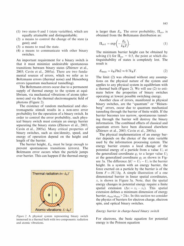
supply of thermal energy to the system at equi-librium, via mechanical vibrations of atoms (pho-nons) and via the thermal electromagnetic field ofphotons (Figure 2).The existence of random mechanical and elec-
tromagnetic stimuli results in a non-zero errorprobability for the operation of a binary switch. Inorder to control the error probability, each phys-ical binary switch must contain an energy barrierseparating the binary states (Zhirnov et al., 2003;Cavin et al., 2005a). Many critical properties ofbinary switches, such as size/density, speed, andenergy of operation depend on the height andlength of the barrier.The barrier height, Eb, must be large enough to
prevent spontaneous transitions (errors). TheBolzmann error occurs when the particle jumpsover barrier. This can happen if the thermal energy
is larger than Eb. The error probability, Perr, isobtained from the Boltzmann distribution as:
Perr1 ¼ exp � Eb
kBT
� �: ð1Þ
The minimum barrier height can be obtained bysolving (1) for Perr = 0.5, the point at which dis-tinguishability of states is completely lost. Theresult is
Ebmin ¼ kBTln2 � 0:7kBT: ð2Þ
The limit (2) was obtained without any assump-tions on the physical nature of the system andapplies to any physical system in equilibrium witha thermal bath (Figure 2). We will use (2) to esti-mate below the properties of binary switchesoperating at lowest possible switching energy.Another class of errors, manifested in physical
binary switches, are the ‘‘quantum’’ or ‘‘Heisen-berg’’ errors, occur due to quantum mechanicaltunneling through the barrier of finite width. If thebarrier becomes too narrow, spontaneous tunnel-ing through the barrier will destroy the binaryinformation. The combined effects of classical andquantum errors have been discussed elsewhere(Zhirnov et al., 2003; Cavin et al., 2005a).The physical implementation of an energy bar-
rier depends on the choice of the state variableused by the information processing system. Theenergy barrier creates a local change of thepotential energy of a particle from a value U1 atthe generalized coordinate q1 to a larger value U2
at the generalized coordinate q2 as shown in Fig-ure 3a. The difference DU ¼ U2 �U1 is the barrierheight. In a system with an energy barrier, theforce exerted on a particle by the barrier is of theform F ¼ @U=@q. A simple illustration of a onedimensional barrier in linear spatial coordinates,x, is shown in Figure 3a. Note, that the spatialenergy changes in potential energy require a finitespatial extension (Dx ¼ x2 � x1). This spatialextension defines a minimum dimension of energybarrier, amin:amin>2Dx. In this section we considerthe physics of barriers for electron charge, electronspin, and optical binary switches.
Energy barrier in charge-based binary switch
For electrons, the basic equation for potentialenergy is the Poisson equation
Figure 2. A physical system representing binary switchimmersed in a thermal bath with two components: radiationand atomic vibrations.
843

r2u ¼ qe0; ð3Þ
where q is the charge density, e0 = 8.85�10)12 F/m is the permittivity of free space, and / is thepotential: / = U/e. According to (3), the pres-ence of an energy barrier is associated withchanges in charge density in the barrier region.The barrier-forming charge is introduced in amaterial e.g. by doping of semiconductors. This isillustrated in Figure 3b, for a silicon n-p-nstructure where the barrier is formed by ionizedimpurity atoms such as P+ in the n-region andB) in the p-region. The barrier height depends onthe concentration of the ionized impurity atoms(Sze, 1981)
Eb � kBTlnN�AN
þB
ni; ð4Þ
where NA), NB
+, and ni are the concentration ofnegatively charged impurities (acceptors), posi-tively charged impurities (donors), and the intrin-sic carrier concentration in a semiconductor,respectively.The minimum barrier extension is given by the
Debye length (Sze, 1981):
LD �ffiffiffiffiffiffiffiffiffiffiffiffiffiffie0ekBTe2N
r; ð5Þ
where e is the relative dielectric permittivity of asemiconductor, and N ¼ N�A ¼ NþB (abrupt p–n
x
(x)
x1 x2
2
1
—j
j
j
j
j ==dx
dF
n n
p
a b
Figure 3. An illustration for the energy barrier in a material system: a – abstraction; b – physical implementation by doping ofsemiconductor.
junction approximation). The maximum concen-tration of electrically active dopants Nmax is closeto the density of states in the conduction, Nc, andvalence bands, Nv of the semiconductor. For sili-con, Nmax� 1019 cm)3 (Sze, 1981), correspond-ingly LD min� 1.3 nm. The minimum barrierlength therefore is amin = 2LD min� 2.6 nm.To enable electron movement between these two
states, the barrier height must be suppressed fromEb to zero. To do this, the amount of charge in thebarrier region needs to be changed. A well-knownrelation connects the electrical potential differenceD / = V and charge, Dq, through capacitance
C ¼ DqDu
: ð6Þ
Thus, operation of all charge transport devicesinvolves charging and discharging capacitances tochange barrier height thereby controlling chargetransport in the device. When a capacitor C ischarged from a constant voltage power supply, theenergy Edis is dissipated, i.e. converted into heat(Cavin et al., 2005b)
Edis ¼CV2
2: ð7Þ
The minimum energy needed to suppress the bar-rier (by charging the gate capacitor) is equal to thebarrier height Eb. Restoration of the barrier (bydischarging gate capacitance) also requires aminimum energy of Eb. Thus the minimum energyrequired for a full switching cycle is at least 2Eb.
844

Next, in order to enable rapid and reliable transi-tion of an electron from state ,0’ to state ‘1’, anenergy asymmetry between two wells needs to becreated. From the distinguishability arguments(Zhirnov et al., 2003; Cavin et al., 2005a), it is easyto show that both the minimum barrier height Eb
and the needed energy difference, DEw, betweentwo wells are given by (2). If N is the number ofelectrons involved in the switching transitionbetween two wells, the total minimum switchingenergy is
ESWmin¼ 2Eb þNDEw ¼ Nþ 2ð ÞkBTln2 ð8aÞ
If N=1,
ESWmin¼ 3kBTln2 � 10�20 J ð8bÞ
Figure 4 displays ITRS data on the switchingenergy and gate length of FETs. It also shows theprojected scaling trend. Note that the trend line, asan extrapolation of experimental data, ends at aswitching energy of 3kBT, consistent with (8b).The extrapolated critical dimension of a FET,corresponding to the smallest switching energy, is�1 nm, in good agreement with theoretical esti-mates (Zhirnov et al., 2003; Cavin et al., 2005a).Practically, the gate length of FET at the end ofscaling is believed to be about 5 nm (ITRS, 2005),not too far from the fundamental limit (Zhirnovet al., 2003; Cavin et al., 2005a). Figure 4 showsthat CMOS scaling is close to optimal for electronbased devices. Replacement devices must be com-petitive (size, speed and energy) with charge-basedbinary switches, which implies operational char-acteristics better then in charge-based devices.
Energy barrier in spin-based binary switch
In addition to charge, e, electrons possess intrinsicangular momentum (spin). As result, they alsopossess a permanent magnetic moment (Singh,1997):
ls ¼ �1
2g � lB; ð9Þ
where lb is the Bohr magneton, lB ¼ e�h=2me ( �h isPlanck constant and me is electron mass), and g isthe coupling constant known as the Lande gyro-magnetic factor or g-factor. For free electrons andelectrons in isolated atoms g0=2.00. In solids,consisting of a large number of atoms the effectiveg-factor can be different from g0.The energy of interaction, El-B, between a
magnetic moment ~l and a magnetic field ~B is:
El�B ¼ �~l � ~B: ð10Þ
For the electron spin magnetic moment in amagnetic field applied in the z direction, the energyof interaction takes two values depending ofwhether the electron spin magnetic moment isaligned or anti-aligned with the magnetic field.From (9) and (10) one can write, assuming g=2
E"" ¼ � e�h2me� Bz;
E"# ¼ þ e�h2me� Bz�
ð11Þ
The energy difference between the aligned andanti-aligned states represents the energy barrier inthe spin binary switch and is
Eb ¼ E"# � E"" ¼ 2lBBz: ð12Þ
Equations (11) and (12) represent a physical phe-nomenon known as Zeeman splitting (Singh,1997). The operation of a single spin binary switchis illustrated in Figure 5. In the absence of anexternal magnetic field, there is equal probabilitythat the electron has magnetic moment +lB or)lB, i. e. the two states are indistinguishable(Figure 5a). When an external magnetic field isapplied (Figure 5b, c), the two states are sepa-rated. The lower energy state has higher proba-bility of population and it represents the binarystate ‘1’ (Figure 5b) or ‘0’ (Figure 5c) in this sys-tem. Binary switching occurs when the externalmagnetic field changes direction as shown inFigure 5b and c.
0.000001
0.00001
0.0001
0.001
0.01
0.1
1
10
100
0.001 0.01 0.1 1
LGATE (µm)
Sw
itchi
ng E
nerg
y(fJ
)
2018
3kBT 10–20 J
2006
≈
Figure 4. Switching energy trend as a function of MOSFETgate length.
845

This abstraction, while very simple, applies to alltypes of spin devices, at equilibrium with thethermal environment, including, e.g. proposedspin transport devices (Daughton, 1997; Jansen,2003; Pearton et al., 2005) and coupled spin-polarized quantum dots (Bandyopadhay, 1994).An energy barrier framework for the spin based
switches helps to understand some fundamentalconstrains of spintronic devices (Zhirnov & Cavin,2006). The barrier-forming magnetic field B can beeither a built-in field formed by a material layerwith a permanent magnetization, or created by anexternal source (e.g. electromagnet). In both cases,the change in the direction of the magnetic fieldrequired for binary switching is produced by anelectric current pulse in one of two oppositedirections. The need for two opposite directions ofelectrical current requires additional electricalbinary switches.Generic electrical circuits to manipulate the
barrier height are a spintronic binary switch isshown in Figure 6. They require four electricalbinary switches in the case of single power supply(Figure 6a) or two binary switches in the case oftwo power supplies (Figure 6b).Thus each spin-based binary switch needs two
or four ‘‘servant’’ charge-based binary switches.This will result in larger area per device and alsolarger energy consumption per operation, ascompared to the charge-based switches. Since theminimum switching energy of one charge-baseddevice is �3kBT according to (8b), the minimumswitching energy of a spin device Espin for singlepower supply scheme is
Espin ¼ e"# þ 12kBT; ð13Þ
where e"# is the ‘‘intrinsic’’ energy to change thespin state. It depends on the specific geometry andthe scheme for generating the magnetic field.One possible direction to address the ‘‘electri-
cal’’ challenge for spin devices is to change the spincontrol paradigm. The paradigm described aboveuses a system of binary switches, each of which canbe independently controlled by an external stimu-lus, and each switch can, in principle control anyother switch in the system. Can a spin state baseddevice be used to control the state of subsequent
B B
‘1’
‘0’
Eb Eb
‘1’
‘0’
ba c
Figure 5. An abstract model of a single spin binary switch: (a) B = 0, two states are insdistinguishable; (b, c) B „ 0, twobinary states are separated by energy gap Eb.
I I
a b
Figure 6. A generic electrical circuit to control spin binaryswitch: (a) single power supply scheme; (b) double powersupply scheme.
846

spin devices without going through an electricalswitching mechanism as discussed above? Perhapslocal interactions can be used to advantage for thispurpose (Bandyopadhay, 1994; Cowburn & Wel-land, 2000). Feasibility assessments of these pro-posals in general information processingapplications are needed.Let us now consider a hypothetical single spin
binary switch that ideally might have atom-scaledimensions. At thermal equilibrium there is aprobability of spontaneous transition between spinstates ‘1’ and ‘0’ in accordance to (1). Corre-spondingly, for Perr<0.5, according to (2) theenergy separation between to state should be lar-ger than kBT ln2
2lBBmin ¼ kBT ln2: ð14Þ
From (2) and (12) one can obtain the minimumvalue of B for a switch operation
Bmin ¼kBT ln2
2lB
¼ me
e�hkBT ln2: ð15Þ
At T = 300 K Eq. (15) results in Bmin� 155 T.This is much larger than can be practicallyachieved (A summary of technologies to generatehigh magnetic fields is given in Table 1).One of the most difficult problems of very high
magnetic field is the excessive power consumptionand Joule heating in electromagnets. The relationbetween power consumption, P, and magnetic fieldB of a electromagnet is (Motokawa, 2004):
P � B2 ð16Þ
and producing magnetic fields e.g. B>10 Trequires many mega-watts of power. As result,these magnetic field production systems have largedimensions and a mass of many tons (see Table 1).
Thus, we conclude that single electron spindevices operating at room temperature wouldrequire local magnetic fields higher than have beenachieved to date with large volume apparatus.In multi-spin systems, it is possible to increase
the magnetic moment l and therefore, to decreasethe magnitude of the external magnetic field Brequired for binary switch operation. The increaseof l can be due to an increase in number of co-aligned spins, which results in collective effectssuch as paramagnetism and ferromagnetism.In a system of N spins in an external magnetic
field, there are N›› spin magnetic moments par-allel to the external magnetic field, and theresulting magnetic moment is
l ¼ lB �N"" ¼ lBN 1�Perrð Þ
¼ lBN 1� exp � lBB
kBT
� �� �: ð17Þ
As we saw above for all practical caseslBB� kBT, and since (1)ex) � x, for x fi 0,there results
l � Nl2BB
kBT: ð18Þ
Equation (18) is known as the Curie law forparamagnetism (Singh, 1997). From (18) and (12)one can calculate the minimum number of electronspins needed for spin binary switch operating atrealistic magnitudes of the magnetic field
Nmin �ln2
2
kBT
lBB
� �2
: ð19Þ
For example, for B = 0.1 T (small neodymium-iron-boron magnet, see Table 1), Nmin � 7� 106.If the number of electrons with unpaired spins peratom is f (f varies between 1 and 7 for different
Table 1. Examples of practical implementations of the sources of magnetism
Magnet B P Mass Comments
Small bar magnet �0.01 T – �gSmall neodymium–iron–boron magnet �0.2 T – �gBig magnetic-core electromagnet �2 T �100 W �kgSteady-field superconductingelectromagnet (Lietzke, 2005)
�16 T �MW �tons Cryogenic temperatures
Current status of Pulse Magnet Programat National High Magnetic FieldLaboratory (Marshall et al., 2004)
60–65 T �MW �tons Cryogenic temperatures;a 30 min cooling time betweenshots; lifetime �400 cycles
847

atoms), the number of atoms needed is Nmin/f.Correspondingly, one can estimate the minimumcritical dimension amin of the binary switch
amin �Nmin
f � n
� �13
; ð20Þ
where n is the density of atoms in the materialstructure. Assuming an atomic density close to thelargest known in solids n� 1023 cm)3 andB� 0.1 T, we obtain amin� 41 nm for f = 1 andamin � 22 nm for f = 7. Thus we conclude that forreliable operation at moderate magnetic fields, thephysical size of multi-spin based binary switch islarger than the ultimate charge-based devices. Theeffect of collective spin behavior is currently usedin e.g. MRAM and in electron spin resonance(ESR) (a practical sensitivity limit of ESR is �1012spins at room temperature).
Energy barriers in optical binary switch
Optical digital computing was and still is consid-ered by some as a viable option for massiveinformation processing (Wherrett, 1996). Some-times it is referred as ‘‘computing at speed of light’’(Higgins, 1995). Indeed, photons move at thespeed of light. At the same time, a photon cannothave speed other then the speed of light, c, andtherefore it cannot be confined within a binaryswitch of finite spatial dimensions.The minimum dimension of optical switch is
given by the wave length of light, k. If amin<k,there is high probability that the light will not‘sense’ the state, i.e. the error probability willincrease. For visible light, amin� 400 nm.Binary state control in the optical switch is
accomplished by local changes in optical proper-ties of the medium, e.g. refraction index, reflec-tivity, or absorption, while photons are being usedto read the state. In many cases, the changes inoptical properties are related to a rearrangementof atoms under the influence of electrical, opticalor thermal energy. The energy barrier in this caseis therefore related to inter-atomic or inter-molecular bonds. Examples of such opticalswitches are liquid crystal spatial light modulators(Wherrett, 1996) and nonlinear interference filters(Wherrett, 1996). Another approach to energybarriers in optics is to change the refractive index
as result of crystalline-to amorphous phasechange, which is used e.g. in the re-writable CD.The minimum switching energy of this class ofoptical switches is related to the number of atoms,N, and therefore to the size L. In the limiting case,L � amin � k. In order for atoms of an opticalswitch to have a distinguishable change of theirposition, the energy supply to each atom should belarger than kBT. The total switching energy istherefore:
E � N � kBT ð21Þ
For minimum energy estimate, we consider thesmallest possible N, which corresponds to an sin-gle-atom plane of size k. If optical switch materialshave atomic density n, one obtains:
E � n23 � k2 � kBT ð22Þ
For most solids, n = 1022–1023 cm)3. Takingn = 5�1022 cm)3, T = 300 K, and amin� 400 nmobtain E� 1014 J. This is in agreement with esti-mates of physical limit of switching energy ofoptical digital switches, given in the literature(Wherrett, 1996).Another class of optical switches are based on
electroabsorption. In these devices, the absorptionchanges by application of an external electric fieldthat deforms the energy band structure. Oneexample that attracted considerable interest forpractical application is the Quantum-ConfinedStark Effect (Miller et al., 1984a). If an electricalfield is applied to a semiconductor quantum well,the shape of the well is changed (e.g. from rect-angular to triangle). As result, the position ofenergy levels also changes, and this effects opticalabsorption. Since formation of an electric fieldrequires changes in charge distribution (Eq. 3), theanalysis of electroabsorption optical switch isanalogous to a charge-based switch, where theenergetics is determined by charging and dis-charging of a capacitor (Eqs. (6) and (7)). Notethat the capacitance of optical switch is consider-ably larger then the capacitance of electron switchbecause of larger capacitance area of the opticalswitch (�k2). Using the estimated minimum size ofan electron switch aemin� 1 nm (Zhirnov et al.,2003; Cavin et al., 2005a), and taking into account(9), we obtain an estimate for the switching energyof an electroabsorption device:
848

E � 3kBTk2
a2emin
� 1:2 � 10�20 J � 400 nmð Þ2
1 nmð Þ2
� 10�15 J ð23Þ
The result (23) is in an agreement with estimates ofphysical limit of electro-absorption optical switch,which is given in the literature (Wherrett, 1996;Miller et al., 1984b).This energy barrier, and therefore the switching
energy for optical binary switch is relatively high:the estimate for theoretical limit for opticaldevice switching energy varies between 10)14 and10)15 J, for different types of optical switches(Wherrett, 1996). The switching speed is the speedof re-arrangement for atoms or for charge in thematerial, and it is not related to the speed of light.
Devices operated out of thermal equilibrium
As we have seen from the previous section, anelementary bistable switch can be described at anabstract level in terms of a statistical mechanicalsystem with one degree of freedom and at least twoallowed energy states. If the binary switch is inthermal equilibrium, the distribution functioncharacterizing the system will be a Boltzman dis-tribution (1), which results in minimum switchingenergy kBTln2, (2). At this level of abstraction, allbinary switches appear equal and would be gov-erned by the kBTln2 switching limit. However, aswe search for alternative ways to physically rep-resent information in future computing systems, itis appropriate to re-examine the critical assump-tions in the thermodynamic argument to see if thesame level of abstraction is indeed still appropri-ate. One principle assumptions is that the switchsystem is at thermal equilibrium with a surround-ing thermal reservoir characterized by the tem-perature T. This implies that there is enough timebetween switching events to allow the thermalequilibration process to take place.George Bourianoff (Bourianoff & Nikonov,
2005) pointed out that virtually all the classicalliterature relating to energy of computationassumed that the logic system had time to ther-mally equilibrate between switching events. Sincethe length and time scales for nano electronicdevices being considered are the in the same orderas thermal scale lengths and times, the fundamental
conclusions relating energy levels to ambient tem-perature need to be re-examined. In the samecontext, the presentation pointed out the couplingof ambient thermal energy to magnetic systems (i.e.the effective noise level) was weaker for magneticsystems than charge based systems. The overallconclusion was that non equilibrium systems werevery common in nature and consideration of suchsystems theoretically removed one of the limitsassociated with classical charge based systems.It was also pointed out that it is possible to read
and write isolated nuclear spin polarized stateswhich maintain themselves in a non-equilibriumenergy configuration for time scales on the orderof minutes (Datta, 2005). These systems have beenexperimentally demonstrated in GaAs/AlGaAssystems in the form of the so called ‘‘HyperfineBattery’’ which reads and writes the nuclear spinstares through the quantum Hall effect (Wurtzet al., 2005).The concept of devices operating out of equi-
librium with the thermal environment has not beenyet adequately explored. A detailed analysis ofbinary switch operation for different state variablesin the case where the switch is not at equilibriumwith thermal environment is needed to ascertain ifthere are performance benefits in this case.
Abstractions for connected binary switches
Devices must communicate with one another tosupport computation, and there is an energy costassociated with communication. In charge baseddevices this implies that when the electron passesfrom state ‘0’ to state ‘1’ in one binary device(sending), it needs to control several other devices(receiving). The gates of these receiving devices areelectrically coupled to at least one well of the firstdevice (Figure 6). To model this, the length of thesending well is extended to accommodate the gatesof receiving devices. In practice, this extension isachieved by interconnect systems. The intercon-nect length L depends on the number of receivinggates coupled to the line. From simple geometricalconsiderations, L>2Fa, where a is the barrierwidth in a binary device and F is number ofreceiving devices, or fan-out. We now assess howreliably the charge in the extended well of thesending device A in Figure 7 controls the receivingdevices B and C. Assume that one electron is
849

needed to control the barrier of each receivingdevices, and one electron passes from one well toanother in 0–1 switching (N = 1) of the sendingdevice. After device A switched to ‘1’ state, there isone electron on the right-hand well of A.The electron can freely move along the line of
length L and the probability to find it only in thegate B or only in the gate C is given by
PB ¼ PC ¼a
L<
a
4a¼ 1
4ð24Þ
To increase the probability of successful control,the number of electrons, N, in the interconnect lineneeds to be increased:
PB ¼ PC ¼ 1� 1� a
L
� �Nð25Þ
For logic operation, a binary switch needs tocontrol at least two other binary switches. Theprobability that N electrons in the interconnectline of device A will be found in the gates of both Band C is:
PB andC ¼ PB �PC ¼ P2 ¼ 1� 1� a
L
� �N� �2
ð26Þ
In general,
Pn ¼ 1� 1� a
L
� �N� �F
ð27Þ
If we require the probability of successful controlof all receiving gates to be >50%, then for F = 2we obtain the minimum number of electrons in theline to be Nmin = 5. For F = 4 (typical fan-out inmicroprocessor ICs), Nmin = 14. Using theobtained minimum number of electrons Nmin, wecan calculate from (8a) the minimum switchingenergy of device A. The results for minimum(F = 2) and typical (F = 4) fan-outs are sum-marized in Table 2 where it is shown that energydissipation per device in interconnected circuitswill considerably exceed isolated device dissipa-
tion. For long distances, the energy trade-offs mayfavour non-electrical communication technologies(Yablonovich, 2005).Equations (16)–(19) describe a stationary situa-
tion, when the probability P to find electron in agiven point is not function of time. This impliesthat the charge is already uniformly distributedwithin the conductor. This model can be extendedto include the initial transient processes thatdetermine the velocity of signal propagation.A schematic energy diagram of a metal inter-
connect is shown in Figure 8. Before charge q isinjected, the conductor is in neutral equilibriumstate with minimum electrostatic energy E: q = 0and E = 0 (Figure 8a). When charge is injected atone end of the conductor, the electrostatic energy atthis end increases anddrives the injected electrons tomove to the lower-energy part of the conductorwithaverage velocity vh i (Figure 8b). The conductor inFigure 8b is in charged non-equilibrium state:q „ 0, E>0, vh i > 0. After a time interval Dt, theconductor reaches a charged quasi-equilibrium(stationary) state: q „ 0, E>0, vh i ¼ 0 (Fig-ure 8c). This charged quasi-equilibrium state is thebasis for Figure 7 and Eqs. (24)–(27).The time interval to reach the stationary state
can be estimated as:
Dt � L
vh i ð28Þ
The average charge velocity can be related to theresistance of the conductor R through the Ohm’sLaw:
I ¼ e � ne � vh i � A ¼ V
Rð29Þ
And therefore,
vh i � 1
Rð30Þ
From (28) and (30), we obtain:
Dt � R � C ¼ a � R � L ¼ R � C; ð31Þ
Table 2. Switching energy considering interconnects
Fan out (n) 2 4
Pn = 50% Nmin 5 14ESW min 7kBT ln2 16kBT ln2
Pn = 99% Nmin 17 42ESWmin 19kBT ln2 44kBT ln2
a
a a
L
A
B C
Figure 7. Device abstraction for connected binary switches.
850

where the proportionality constant, a, depends onthe geometry of the conductor.To summarize, increased energy utilization is
required to maximize the probability for intendedtransitions and to minimize the probability ofunintended transitions in electronic informationprocessing systems. This is manifested in devices bythe need for higher (and wider) energy barriers thatmust be manipulated to control device operationsand by the need to provide a sufficient number ofelectrons to assure correct operation of down-stream devices. Again, by increasing the number ofdevice electrons, there is incurred a correspondingincrease in device energy consumption.
Approaching thermal extraction limits
The ability to remove heat has important impli-cations for future computers and, more generally,for nanoelectronic systems. The management ofheat is becoming one of the most fundamentalproblems for the nanoelectonics. In today’s com-puters we deal with heat flows of <100 W/cm2,while in a foreseeable future we may need tomanage heat flows >1000 W/cm2. The purpose ofthis section is to provide insight into those physicalparameters that govern the ultimate limits of heatremoval (Zhirnov et al., 2005a, b).
The maximum rate of heat transfer insidean infinite system
The maximum time rate of energy transfer from anatom to a heat transfer agent (e.g. another atom,
electron or photon) is limited by the HeisenbergPrinciple for time and energy:
DEDt � �h
2; ð32Þ
For thermal energy, the maximum DE � kBT andwe thus obtain for the maximum rate of energytransfer par channel (Heisenberg limit):
_Qmax ¼DEmax
Dtmin¼ 2ðkBTÞ2
�hð33Þ
If energy is transferred by collisions of masses, themaximum density of the collision channels is thenumber of atoms per cross-section, say, ns.Therefore, the rate of heat transfer per unit area isgiven by:
_qmax ¼ ns � _Q ¼ 2ðkBTÞ2
�h� n2
3 ð34Þ
where n is the number of atoms per unit volume.Equation (34) was obtained under the assump-
tions that the temperature of the ‘‘hot’’ side ofthe system T1 = 300 K, while the temperature ofthe ‘‘cold’’ side T2 = 0 K. If the temperatureof the heat receiver T2>0, and the heat is trans-ferred through a heterogeneous interface (i.e.atomic/molecular masses of the heat source andheat receiver are not necssarily the same,m1 „ m2), the mean energy transfer is given by
DEh i ¼ 2l E1b � E2bð Þ¼ 2lðkBT1 � kBT2Þ ¼ 2lkBDT ð35Þ
where l ¼ m1m2
m1þm2ð Þ2
E
xL x xL L
0 0
Neutral Equilibrium
Charged Non-Equilibrium
Charged Quasi-Equilibrium
a b c
0>v 0=v
t
E E
0
∆
Figure 8. Schematic energy diagram of a interconnect conductor.
851

For homogeneous medium (equal mas-ses), l= 0.25, and (33) and (34) will be modifiedas follows:
_Qmax ¼ðkBDTÞ2
2�hð36Þ
_qmax ¼kBDTð Þ2
2�h� n2
3 ð37Þ
We now take into account the fact that the inter-action time between two neighbouring atomsincludes both traverse and contact components.We can obtain a good estimate for the totalinteraction time from the velocity of sound in themedium, vs:
Dt ¼ l
vs¼ n�
13
vsð38Þ
From (35) and (38) we obtain
_Qmax ¼DEDt¼ 2lkBDTvsn
13: ð39Þ
Assuming l= 0.25 (m1 = m2), the heat flow perunit area is
_qmax ¼ _Qmax � n23 ¼ 1
2kBDTvsn ð40Þ
Equations. (39) and (40) represent the maximumrate of heat transfer in the kinetic limit, i.e. takinginto account the traverse time.Table 3 compares maximum heat flows calcu-
lated in Heisenberg and kinetic limits forT1 = 400 K and T2 = 300 K. Values for silicon,air and water are presented.
The maximum amount of heat that canbe transferred outside a finite system
If we consider heat transfer through the interfacebetween medium 1 with the maximum heat trans-
fer rate _q1maxand medium 2 with the maximum
heat transfer rate _q2max, the maximum attainable
interface heat transfer rate is
_q12max¼ min _q1max; _q2max
� �ð41Þ
For example, in the heat transfer from silicon intoair, the maximum heat flux in silicon is 7.6�106 W/cm2, but no more than 650 W/cm2 can be trans-ferred from silicon into air. Thus, the limiting fac-tor for heat transfer at the solid–gas interface is dueto the discontinuity in density of the conductancechannels because there are several orders of mag-nitude difference in atomic density. Thus we con-clude that, by transferring heat from a solid to air,the maximum heat transfer rate cannot exceed �650W/cm2 (Table 3). Note that this maximum numberassumes that in all cases, the hot atoms of the solidcollide with ‘‘cold’’ atoms or molecules, which aremaintained at T2 = 300 K. In case of solid–waterinterface, if after collision with a surface atom,the water molecule absorbs additional energy,DE, and therefore becomes ‘‘warm’’, withT2>300 K. These ‘‘warm’’ water molecules willreduce the energy transfer rate unless removedimmediately.As shown in Table 3, the supply of the heat to
the solid–air or solid–water interface is larger thanthe heat transfer rate in air or in water, because oflarger atomic density and larger speed of sound insolids. Thus the temperature of air/water willincrease and the cooling efficiency will corre-spondingly decrease. To increase cooling effi-ciency, forced liquid cooling could be employed,where the ‘‘warm molecule is forcefully replacedby a ‘‘fresh’’ water molecule at T = 300 K. In thiscase, the cooling rate is determined by the supplyrate of ‘‘cold’’ water molecules.For a liquid flow rate (in m/s) u0 we estimated
the maximum heat transfer rate per channel for theforced liquid cooling to be
Table 3. Maximum heat flows inside an infinite system calculated in Heisenberg and kinetic limits for T1 = 400 K andT2 = 300 K
Medium Speed of
Sound, v [cm/s]
Atomic concentration,
n [cm)3]
_qmax (Heisenberg limit)
[W/cm2]
_qmax (Kinetic limit)[W/cm2]
Si 2.2�105 5.0�1022 1.2�107 7.6�106Water 1.5�105 3.4�1022 9.5�106 3.5�106Air 3.5�104 2.7�1019 8.2�104 6.5�102
852

_Q ¼ DEh iDt¼ l 2kBDT�m2u
20
� �� u0 � n
13
2; ð42Þ
and per unit area
_q ¼ _Q � n23
2 ¼ l 2kBDT�m2u20
� �� u0 � n2: ð43Þ
The maximum of (43) is
_qmax ¼4ln23
ffiffiffiffiffiffiffiffiffiffiffiffiffiffiffiffiffiffiffiffi2 kBDTð Þ3
3m2
s; ð44Þ
and is reached at liquid flow rate
u0max ¼
ffiffiffiffiffiffiffiffiffiffiffiffiffiffi2kBDT3m2
s: ð45Þ
Figure 9a shows the heat transfer rate _qðu0Þ byforced liquid cooling of silicon by water. Thetemperature of silicon surface is T1 = 400 K andthe temperature of water is T2 = 300 K. Forthese conditions, _qmax ¼ 2:6� 105 W=cm2 andu0max ¼ 175m=s1. Equation (44) also applies toforced air cooling. The plot _qðu0Þ for air cooling isshown in Fig, 9b. For this case, _qmax ¼ 172W=cm2
and u0max ¼ 140m=s1.The permanent presence of cold molecules on
the surface can be achieved either by fast replace-ment or by using molecules with internal degreesof freedom (i.e. higher heat capacity). When ther-mal energy is transferred to molecules with addi-tional degrees of freedom, the absorbed energy isequally distributed between all degrees of freedom,and only a fraction of total energy goes to trans-lational degrees of freedom and hence increase
temperature. Therefore, such molecules can expe-rience several energy transfers before their tem-perature increase will be remarkable. Watermolecules have very high heat capacity andtherefore they can longer remain in contact withhot surface before they will need to be replaceddue to temperature increase. As result, the deliveryvelocity u0 in (43) can be lower. A similar effectoccurs during phase change (for example boiling),when breaking cohesive bonds absorb energywithout increase in the temperature. Anotherpositive effect of phase change is fast removal ofmolecules after contact with hot surface. Phasechange cooling processes do not impact the max-imum heat transfer rate at the interface, but theyrather ‘improve’ the properties of cooling agentand thus help to move closer to the upper boundnumbers of Table 3.To conclude this section, the ability to remove
heat from a volume of mass is fundamentally lim-ited by the the maximum amount of heat that canbe ultimately transferred to the ambient, which, e.g. to air or water at T = 300 K. Figure 10 sum-marizes the theoretical limits of heat transferobtained in this section and compares it to thecurrently experimental results for air (ITRS, 2005)and water (Tuckerman & Pease, 1981) cooling. Asfollows from this comparison, for the air cooling,the experimentally achieved level is within an orderof magnitude of the fundamental limit. However,for the water cooling, a there is significant gapbetween experimental achievement and theoreticalprediction. More research is needed to fully exploitthe potential of active water cooling.
020
4060
80100120
140160
180200
0 50 100 150 200 250
u 0 , m/s
q, W
/cm
2
0.0E+00
5.0E+04
1.0E+05
1.5E+05
2.0E+05
2.5E+05
3.0E+05
0 50 100 150 200 250
u 0 , m/s
q, W
/cm
2
a b
Figure 9. Maximum heat removal rate for forced water (a) and air (b) cooling.
853

Nanoengineered materials and fabrication via
directed self assembly
Considerable research is needed before new familiesof nanoengineered materials (NEM) and directedself-assembly (DSA) can be utilized as mainstreamintegrated circuit manufacturing options. Animportant research goal is to demonstrate the fea-sibility of integrating and interconnecting novelengineered nanomaterials and self-assembly meth-ods into IC fabrication processes that enable ordersof magnitude increases in functional density. Thissection focuses on two thematic needs: (1) atomiclevel design and synthetic control of nanoengi-neered materials and architectures and (2) the formand content of information designed into selfassembling materials.
Atomic level design and synthetic controlof nanoengineered materials
By 2020, critical dimensions are projected to be ator less than of 50±5 A for electronic devices(ITRS, 2005). The ability of modern fabricationtools to offer this degree of dimensional control islimited and auxiliary approaches are needed,including new nanoengineered materials and novelfabrication methods. If achieved, this wouldenable the realization of a manufacturing capa-bility that exhibits nanometer resolution withatomic level tolerances.
Recent reports (Chen et al., 2005; Herr, 2005)from other fields hint at paths for uncoveringpotentially breakthrough nanomanufacturingoptions. For example, a recent study of Pd cata-lyzed vinyl acetate synthesis reveals that subtlevariations in Pd–Pd distances effect dramaticchanges in vinyl acetate formation rates (Chenet al., 2005). Figure 11a shows that inter-palla-dium distances in Au(100), 4.08 A, more closelyresembles that of an optimized catalyst, 3.3 A,than does Pd in Au(111), at 4.99 A. Figure 11bindicates that a 0.91 decrease in Pd spacing yields afourfold increase in vinyl acetate formation rates.Though the science of designed atomic architec-
tures is in its infancy, this result suggests the impactthat atomic level design and synthetic control ofnanoengineered materials and architectures wouldhave on the manufacturability of deep nanoscaledevice components, such as atomically designedcatalysts for controlled nanotube growth, deter-ministically doped channels, etc. Consequently,critical dimensional and tolerance projections atand beyond the end of the Roadmap could becomesignificant if novel materials and manufacturingsolutions are discovered that exhibit the requiredatomic architectural and positional control.
The form and content of information designedinto self assembling materials
Directed self assembling materials, such as blockcopolymers, exhibit potential as smart resists for
Solid-Air Solid-Water
2650
max cm
Wq =
2172
cm
Wqair =
2exp 64cm
Wq =.
.
. Coherent heat transfer
Limits of forced liquid/air cooling
Demonstrated
26
max 105.3cm
Wq ×=
25106.2
cm
Wqwater ×=
2exp 700cm
Wq =
10exp
max
q
q5000
exp
max
q
q
.
.
.
≈≈
Figure 10. Prediction/Achievement gap for the heat transfer to the ambient.
854

sub-lithographic patterning. The state-of-the-art,with respect to these self assembling systems, canbe summarized as follows (Black, 2005a):
• High feature density (small size, tight pitch)• Periodic structures• Reasonable size uniformity, little uniformity in
ordering• Some size tenability, but yet to be demonstrated
within a single layer• Robust pattern alignment has yet to be dem-
onstrated
For applications in which many identical elementscomprise a single device, there is no need for par-ticularly good order, uniformity, or registration inthe element formation. An example of such deviceis an on-chip decoupling capacitor (Black et al.,2004). In this application, the self-assembled peri-odic structure can be used to increase surface area.One step up in application complexity is nano-crystal floating gate memory that contains manysublithographic elements (nanocrystals) within gatedielectric (Black, 2005a). In this case, uniformity ofsize and spacing is important for device reproduc-ibility. Recently, a group at IBM reported fabri-cation of a Si nanowire FET with several parallelnanowire channels by directed self-assembly ofcopolymers (Black, 2005b). Critical device dimen-sions (channel width) were defined by self-assemblywithin a lithographically defined template.An important issue in the use of directed SA of
block copolymers is the slowness of the SA pro-cess, relative to conventional lithographic pro-
cesses (Black, 2005a). This question has not beensufficiently discussed by the research communityand we believe that the copolymer SA processspeed needs to be properly addressed. In fact,quantitative assessments are highly desirable forself-assembly that would characterize (a) infor-mational content delivered to the materials struc-ture; (b) the time required for the SA process,which could be described e.g. as process band-width; (c) the energetics of the SA process.At the simplest level, the information embedded
in a materials system is contained in the descrip-tion of material shapes and their composition(Ayres, 1994). For example, a point in 3D-space isdefined by three numbers. A flat surface is com-pletely defined by the four numeric parameters ofthe form (Ayres, 1994):
axþ byþ czþ d ¼ 0 ð46Þ
The information required to specify each numericparameter depends on the precision needed. Theinformation content of a single parametric speci-fication is (Ayres, 1994):
Ipar ¼ log2m
Dmð47Þ
Where m is the dimensional measure and Dm is therequired precision. For example, if the specifiedprecision is 1 ppm, Ipar ¼ log2 10
6 ¼ 20 bit.It is also possible to quantify information
embedded in materials composition. The numberof different atoms available as construction ele-ments of a materials system is given by the number
Figure 11. (a) Schematic for vinyl acetate synthesis from acetic acid and ethylene and (b) Vinyl acetate formation rates as afunction of Pd coverage on Au(100) and Au(111). From Chen et al. (2005), reprinted with permission from AAAS.
855

of elements in the Periodic System, A� 100.Therefore, the information needed to specify aparticular choice of atoms is
Iat � log2 A � log2 100 � 7bit ð48Þ
Using shape-defining equations of the type (46),along with (47) and (48), it is possible, in principle,to calculate the informational content of an arbi-trary materials system. The fabrication process canbe regarded as implementing information deliveryto a material, e.g. through a series of assemblyinstructions. As an example, in the case of litho-graphic patterning, information is delivered bylight modulated by mask. In the case of self-assembly methods, more attention needs to bepaid to the sources and carriers of information.For example, most current self-assembly methodsare based on equilibrium thermodynamics, and asresult information is carried only by few processparameters such as temperature, concentration,pressure molecular/atomic composition etc. Theresulting materials structure has low informationalcontent, for example a periodic array. The amountof information – the ‘‘assembly instructions’’ – canbe considerably increased by using non-equilib-rium processes – where some or all of the processparameters (e.g. temperature, concentration etc),are time-dependent, and can be represented as avector
X ¼x1ðtÞ. . .xnðtÞ
0@
1A ð49Þ
Careful formulations of information embedded inthe material structure as well as the of ‘instructionset’ used for assembly during fabrication areneeded.
Conclusions
The imperative to discover alternative informationprocessing technologies that include binaryswitches and a means for communication betweenswitches has become an imperative if the expo-nential improvements in performance per unit costis to be sustained beyond the limits of charge-based information technology scaling. Theurgency associated with this search is caused bythe long lead times (�12 years) required for tech-
nology insertion by the semiconductor industry. Inthis paper, we have briefly reviewed projectedlimits for scaling of charge, spin, and opticaldevices operating in equilibrium with the thermalenvironment. As a general comment, all of thesedevices are subject to limits that a multiples of kBTswitching energy dissipation due to the Boltzmannproperties of the thermal environment. Thereis hope that if devices can be operated out-of-equilibrium with the thermal environment, thenperhaps computational state variables can bechosen to improve on the kBT switching energycharacteristic of charge-based equilibrium devices.In parallel an aggressive exploration of newarchitectures is needed to achieve orders of mag-nitude improvement in effective ‘‘function-scalability’’.Efficient device communication is required if
useful information processing technologies are tobe developed. In this paper (and at the workshop),the focus was primarily on the limiting propertiesof charge-based interconnections. It is argued thatin the limit, the interconnect systems will requiresignificantly more energy to operate than theswitches themselves. This conclusion does notdepend on the metal/dielectric/barrier system usedto implement the interconnect system and rests onthe localization properties of a few electronsinjected into a conductor. If it were possible toeliminate, or reduce the long interconnects, anorder of magnitude improvement in energy con-sumption might be achieved.Increased component packing densities and
higher operating speeds have made higher a realpower dissipation inevitable, resulting in the needfor enhanced heat management technologies forintegrated circuits. This raises the question ofphysical limits for heat removal; especially forroom temperature air and water cooling systems.An intuitively simple model is given that suggeststhat the relative gains in air cooling capacity thatremain to be obtained are quite modest while watercooling continues to offer the capacity for the twoto three order of magnitude of improvement.One of the most costly manufacturing processes
is patterning and prospects for cost reductions fortop-down methods for nanoscale features are notencouraging. Progress is being made in the use ofself-assembly for block co-polymers as resists toachieve increasingly complex features. It appearsthat line-edge roughness can be improved relative
856

to top-down patterning by self-assembly methods.IBM has reported experimental use of limitedforms of self-assembly in a pre-production facility;however, much research is needed to provide anadequate foundation for the utilization of directedself- assembly in mainstream production of inte-grated circuits. Perhaps an appropriate goal for theuse of self-assembly in nanoelectronic manufac-turing is to approach the very high assembly speed,very high complexity and very low energy costs ofassembly that is observed in living organisms.
Acknowledgements
The authors are grateful to George Bourianofffrom Intel Corp. for his help with Section Devicesoperated out of thermal equilibrium (devicesoperated out of thermal equilibrium) and for athoughtful review of the paper.
References
Ayres R.U., 1994. Information, Entropy, and Progress. AIP
Press: New York.
Bandyopadhay S., B. Das & A.E. Miller, 1994. Supercomputing
with spin-polarized single electrons in a quantum coupled
architecture. Nanotechnology 5, 113–133.
Black C.T., 2005a. Integration of directed self-assembly in
semiconductor microelectronics, Third Workshop on Silicon
Nanoelectronics and Beyond (SNB), December 8–9, 2005,
National Science Foundation, Arlington, VA, USA.
Black C.T., 2005b. Self-aligned self assembly of multi-nanowire
silicon field effect transistors. Appl. Phys. Lett. 87: 163116.
Black C.T., K.W. Guarini, Y. Zhang, H.J. Kim, J. Benedict,
E. Sikorski, I.V. Babich & K.R. Milkove, 2004. High-
capacity, self-assembled metal-oxide-semiconductor decou-
pling capacitors. IEEE Electron Dev.Lett. 25, 622–624.
Bourianoff G.I. & D.E. Nikonov, 2005. Non-equilibrium
systems, alternative state variables and noise considerations.
Third Workshop on Silicon Nanoelectronics and Beyond
(SNB), December 8–9, 2005, National Science Foundation,
Arlington, VA.
Cavin R.K., V.V. Zhirnov, G.I. Bourianoff, J.A. Hutchby,
D.J.C. Herr, H.H. Hosack, W.H. Joyner & T.A. Wooldridge,
2005a. A long-term view of research targets in nanoelectron-
ics. J. Nanoparticle Res. 7, 573–586.
Cavin R.K., V.V. Zhirnov, J.A. Hutchby & G.I. Bourianoff,
2005b. Energy barriers, demons, and minimum energy
operation of electronic devices. Fluctuation Noise Lett. 5,
C29–C38.
Chen M., D. Kumar, C.W. Yi & D.W. Goodman, 2005. The
promotional effect of gold in catalysis by palladium-gold.
Science 310, 291–293.
Cowburn R.P. & M.E. Welland, 2000. Room temperature
magnetic quantum cellular automata. Science 287, 1466–
1468.
Datta S., 2005. Non-equilibrium systems: computational state
vectors other than charge. Third Workshop on Silicon
Nanoelectronics and Beyond (SNB), December 8–9, 2005,
National Science Foundation, Arlington, VA, USA.
Daughton J.M., 1997. Magnetic tunneling applied to memory.
J. Appl. Phys. 81, 3758.
Herr D., 2005. Novel materials and assembly methods for
extending charge-based technology to its ultimate limits,
Third Workshop on Silicon Nanoelectronics and Beyond
(SNB), December 8–9, 2005, National Science Foundation,
Arlington, VA, USA.
Higgins T.V., 1995. Computing with photons at the speed of
light. Laser Focus World 31, 72–77.
ITRS, 2005: Semiconductor Industry Association (SIA), Inter-
national Technology Roadmap for Semiconductors 2005
edition. International SEMATECH, Austin, TX.
Jansen R., 2003. The spin-valve transistor: a review and
outlook. J. Phys. D – Appl. Phys. 36, R289–R308.
Lietzke A.F., S.E. Bartlett, P. Bish, S. Caspi, D. Dietrich,
P. Ferracin, S.A. Gourlay, A.R. Hafalia, C.R. Hannaford, H.
Higley, W. Lau, N. Liggins, S. Mattafirri, M. Nyman, G.
Sabbi, R. Scanlan & J. Swanson, 2005. Test results of HD1b,
and upgraded 16 Tesla Nb3Sn Dipole Magnet. IEEE Trans.
Appl. Supercond. 15, 1123–1127.
Marshall W.S., C.A. Swenson, A. Gavrilin & H.J. Schneider-
Muntau, 2004. Development of ‘‘Fast Cool’’ pulse magnet
coil technology at NHMFL, Physica B 346: 594–598. See also
the National High Magnetic Field Laboratory website at:
http://www.magnet.fsu.edu/magtech/core.
Miller D.A.B., D.S. Chelma, T.C. Damen, A.C. Gossard,
W. Wiegmann, T.H. Wood & C.A. Burrus, 1984a. Band-edge
electroabsorption in quantum well structure: the quantum-
confined Stark effect. Phys. Rev. Lett. 53, 2173–2176.
Miller D.A.B., D.S. Chelma, T.C. Damen, A.C. Gossard,
W. Wiegmann, T.H. Wood & C.A. Burrus, 1984b. Novel
hybrid optically bistable switch: the quantum well self-
electro-optic effect device. Appl. Phys. Lett. 45, 13–15.
Motokawa M., 2004. Physics in high magnetic fields. Rep.
Prog. Phys. 67, 1995–2052.
Pearton S.J., D.P. Norton, R. Frazier, S.Y. Han, C.R.
Abernathy & J.M. Zavada, 2005. Spintronics device con-
cepts. IEE Proc.-Circ. Dev. Syst. 152, 312–322.
Roco M.C., 2006. National nanotechnology investment in the
FY 2007 budget request. In: AAAS Report on U.S. R&D in
FY 2007, Washington, D.C., March 2006.
Singh J., 1997. Quantum Mechanics – Fundamentals and
Applications to Technology, John Wiley & Sons.
Sze S.M., 1981. Physics of Semiconductor Devices. John Wiley
& Sons.
Tuckerman D.B. & R.F.W. Pease, 1981. Implications of high-
performance heat sinking for electron devices. IEEE Trans.
Electron Dev. 28, 1230–1231.
Wherrett B.S., 1996. Materials for optical computing. Synthetic
Metals 76, 3–9.
857

Wurtz A., T. Muller, A. Lorke, D. Reuter & A.D. Wieck, 2005.
Electrical readout of the local nuclear polarization in the
quantum hall effect: A hyperfine battery. Phys. Rev. Lett. 95,
056802 .
Yablonovitch E., 2005. The impedance matching predicament
in intra–chip communication, Third Workshop on Silicon
Nanoelectronics and Beyond (SNB), December 8–9, 2005,
National Science Foundation, Arlington, VA, USA.
Zhirnov V.V. & R.K. Cavin, 2006. An energy barrier frame-
work for the limits of charge and spin based switches,
J. Nanoelectron. Optoelectron. (to be published).
Zhirnov V.V., R.K. Cavin, J.A. Hutchby & G.I. Bourianoff,
2003. Limits to binary logic switch scaling – a Gedanken
model. Proc. IEEE 91, 1934–1939.
Zhirnov V.V., A. Avila & R.K. Cavin, 2005a. Fundamentals of
heat removal: limits and opportunities, Third Workshop on
Silicon Nanoelectronics and Beyond (SNB), December 8–9,
2005, National Science Foundation, Arlington, VA, USA.
Zhirnov V.V., A. Avila & R.K. Cavin, 2005b. Fundamentals of
heat transfer, Internal SRC working paper.
858