Reducing Device Stress and Switching Losses Using Active ...
217
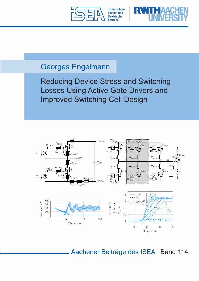
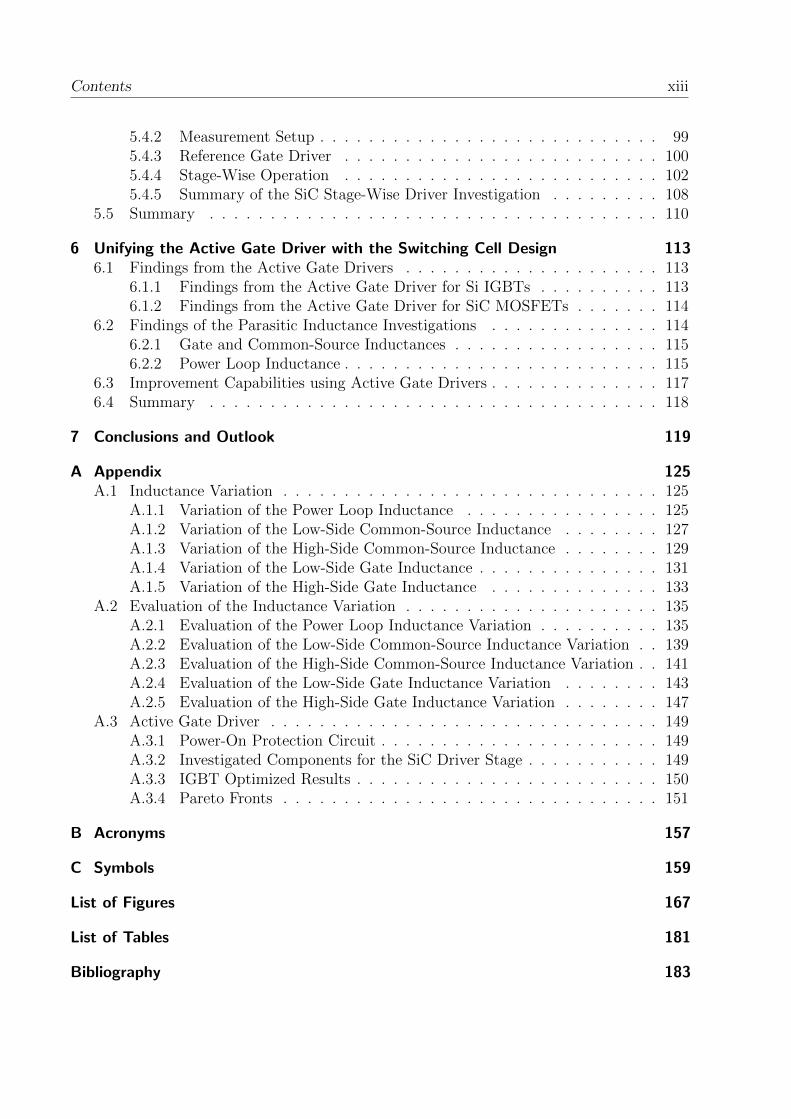
Aachener Beiträge des ISEA Georges Engelmann Reducing Device Stress and Switching Losses Using Active Gate Drivers and Improved Switching Cell Design Band 114 U cc u GS C DC R G,HS R G,LS L G,HS L G,LS L CS,HS L CS,LS ΔL Loop S 1 S 2 Lσ/2 Lσ/2 DC+ DC- SW L σ,CVR R CVR u GS,HS U cc i S U GS,on U GS,off R g,on,1 Q off,1 u GS S DUT i Drain i G Q on,1 R g,on,2 R g,on,n R g,off,2 R g,off,n R g,off,1 Q off,2 Q off,n Q on,2 Q on,n IC 1,B IC 1,A IC 2,A IC n ,A IC 2,B IC n ,B i S Single branch 0 50 100 150 0 200 400 600 800 Time in ns Voltage in V 0 20 40 60 0 0.2 0.4 0.6 0.8 Time in ns u DS in kV i S in kA E off in mJ u DS i S ´ p SW dt ❳ ❳ ❳ ❳ ❳❳ ③ ✻ ❇ ❇ ❇ ◆ E off ˆ U DS
-
Upload
khangminh22 -
Category
Documents
-
view
0 -
download
0
Transcript of Reducing Device Stress and Switching Losses Using Active ...
Aachener Beiträge des ISEA
Georges Engelmann
Reducing Device Stress and Switching Losses Using Active Gate Drivers and Improved Switching Cell Design
Band 114
Ucc
uGS
CDC
RG,HS
RG,LS
LG,HS
LG,LS
LCS,HS
LCS,LS
∆LLoop
S1
S2
Lσ/2
Lσ/2
DC+
DC−
SW
Lσ,CVR
RCVR
uGS,HS
Ucc
iS
UGS,on
UGS,off
Rg,on,1
Qoff,1
uGS
SDUTiDrain
iG
Qon,1
Rg,on,2 Rg,on,n
Rg,off,2 Rg,off,nRg,off,1
Qoff,2 Qoff,n
Qon,2 Qon,n
IC1,B
IC1,A IC2,A ICn,A
IC2,B ICn,B
iS
Single branch
0 50 100 150
0
200
400
600
800
Time in ns
Voltage
inV
0 20 40 60
0
0.2
0.4
0.6
0.8
Time in ns
uDSin
kV
i Sin
kA
Eoffin
mJ
uDS
iSpSWdt
Eoff
UDS
1

Reducing Device Stress and SwitchingLosses Using Active Gate Drivers and
Improved Switching Cell Design
Von der Fakultat fur Elektrotechnik und Informationstechnikder Rheinisch-Westfalischen Technischen Hochschule Aachen
zur Erlangung des akademischen Grades eines Doktors derIngenieurwissenschaften genehmigte Dissertation
vorgelegt von
Diplom-Ingenieur
Georges Engelmann
aus Wiltz, Luxembourg
Berichter:
Univ.-Prof. Dr.-Ir. Dr.-h. c. Rik W. De Doncker
Univ.-Prof. Dr.-Ing. Stefan Heinen
Tag der mundlichen Prufung: 11. Juli 2018
Diese Dissertation ist auf den Internetseitender Hochschulbibliothek online verfugbar.


Georges Engelmann
Reducing Device Stress and Switching Losses Using Active Gate Drivers and
Improved Switching Cell Design
Electronic version The electronic version is available online on the institutional repository of RWTH Aachen University (https://publications.rwth-aachen.de). AACHENER BEITRÄGE DES ISEA Vol. 114 Editor: Univ.-Prof. Dr. ir. h. c. Rik W. De Doncker Director of the Institute for Power Electronics and Electrical Drives (ISEA), RWTH Aachen University Copyright ISEA and Georges Engelmann 2018 All rights reserved. No part of this publication may be reproduced, stored in a retrieval system, or transmitted in any form or by any means, electronic, mechanical, photocopying, recording, or otherwise, without prior permission of the publisher. ISSN 1437-675X Institut für Stromrichtertechnik und Elektrische Antriebe (ISEA) Jägerstr. 17/19 • 52066 Aachen • Germany Tel: +49 (0)241 80-96920 Fax: +49 (0)241 80-92203 [email protected]

Preface (Vorwort)
Diese Arbeit entstand im Rahmen meiner Tatigkeiten als wissenschaftlicher Mitarbeiteram Institut fur Stromrichtertechnik und Elektrische Antriebe (ISEA) der RWTH Aachen.Zunachst mochte ich mich bei meinem Doktorvater, Herrn Prof. De Doncker, fur die Moglich-keit bedanken, dass ich als wissenschaftlicher Mitarbeiter an seinem Institut an meinemDissertationsthema forschen konnte. Ebenso bedanke ich mich fur die großen Freiraume,die mir bei der eigenstandigen wissenschaftlichen Arbeit eingeraumt wurden. Herrn Prof.Heinen danke ich fur die Ubernahme des Korreferats.
Ich danke außerdem dem Bundesministerium fur Bildung und Forschung (BMBF) fur die fi-nanzielle Unterstutzung durch diverse Projekte sowie der Ford Motor Company in Dearborn,USA fur die exzellente Kooperation, die finanzielle Unterstutzung und die unkompliziertenfreigaben zum Veroffentlichen verschiedener Paper und dieser Dissertation.
Die Zeit am ISEA hat mir sehr viel Spaß gemacht und es bleiben fast ausschließlich positiveErinnerungen. Bei allen Kollegen bedanke ich mich fur das außerst angenehme Arbeitsklimasowie den Zusammenhalt in der Gruppe. Das konstruktive Miteinander und Fureinanderist es, was das ISEA ausmacht. Ich danke meinen langjahrigen Burokollegen Furkan KaanTitiz, Martin Rosekeit, Marcus Conrad, Christoph Ludecke und Philipp Schulting fur diegemeinsame Zeit. Hauke van Hoek, Matthias Biskoping, Stefan Engel, Bernhard Burkhart,Markus Neubert, Annegret Klein-Heßling und Michael Schubert danke ich fur die Arbeitenals Gruppenleiter und Oberingenieure wahrend meiner Zeit am ISEA. Claude Weiss undKarl Oberdieck danke ich fur die angenehme Zusammenarbeit in gemeinsamen Projekten.Bei Jan Gottschlich bedanke ich mich fur die gute Zusammenarbeit aber auch fur den vonihm gebauten Doppelpulsprufstand, ohne welchen diese Dissertation nicht in dem gegebenenUmfang zustande gekommen ware. Neben den diversen sozialen Aktivitaten danke ich demB12 fur den wochentlichen Ausgleich vom Tagesgeschaft. Iliya Ralev danke ich fur diegemeinsame Zeit am ISEA, sowie fur die gegenseitige Motivation zum Zusammenschreibendieses Werks.
Ich mochte mich ausßerdem herzlichst bei allen Studenten bedanken fur die tatkraftige Un-terstutzung bei der Projekt- und Dissertationsarbeit im Rahmen von Bachelor- und Master-arbeiten sowie HiWi-Stellen: Tizian Senoner, Christoph Ludecke, David Bundgen, MichaelLaumen, Stefan Quabeck, Jan Niklas Fritz, Philipp Schnorr von Carolsfeld, Severin Kleverund Guido Bollmann. Christoph, Michael, Stefan, David und Niklas danke ich weiterhin furdie gemeinsamen Arbeiten als sie spater Kollegen waren. Bei Christoph und Stefan bedankeich mich fur das Korrekturlesen der Dissertation.

Meinen Eltern danke ich fur die Forderung vielfaltiger Interessen, stetige Unterstutzungund Ermoglichung zum Studium. Meiner lieben Freundin Dijana Sehic danke ich fur dieUnterstutzung und den Ruckhalt wahrend den letzten Monaten vor der Abgabe.
Aachen, im September 2018 Georges Engelmann
Abstract
Today’s power converter designs, especially in the automotive or the all-electrical aircraftindustry, aim at higher power densities. These goals can be achieved with an increasedintegration level and a transition from silicon insulated-gate bipolar transistors (IGBTs) tofast switching wide-bandgap (WBG) devices.
The aims of this thesis are to investigate the influence of the packages and the drivingcircuits on the switching behavior of silicon (Si) IGBTs and silicon carbide (SiC) metal-oxidesemiconductor field-effect transistors (MOSFETs). The peak voltages and surge currentsduring switching determine the stress on the devices. The stress depends on several parasiticelements in and around the switching cell and the gate driving circuitry. A reduction of thestress could result in the possibility to utilize a higher dc-link voltage or increased efficiency,and thus, lead to significant cost reduction.
First, simulative and measurement techniques to identify and parametrize inductive andcapacitive parasitics of the packages are shown. The presented concepts are demonstratedusing a power module package and a common package of a discrete power semiconductor.As such, a wide range of different power electronics packages are covered in this thesis.
In a second step, the influence of the different parasitic inductive elements on the switchingtransients is investigated. Therefore, a switching cell using variable inductive elements isdeveloped. The variable inductive elements are the loop, gate and common-source induc-tances for both, the low- and high-side switches. The impact of each inductive element onthe switching behavior is investigated regarding the stress on the device and the resultingswitching losses. The limitations of the cell design on the switching performance and thecauses for the observed oscillations are identified. Conclusions are drawn for improved powermodule designs for low- and medium-voltage applications.
To influence the switching behavior of the device, a switched resistor, stage-wise gate driveris designed for a silicon IGBT power module, and a SiC MOSFET switching cell. The chal-lenges of an active gate driver design for fast switching wide-bandgap power semiconductorsand the challenges of high-bandwidth voltage and current measurements are discussed. Forboth, the IGBT and the SiC MOSFET, the stresses are reduced while maintaining equalswitching losses. It is shown that the switching transients can be manipulated to balancedevice stresses and switching losses.
The use of active gate drivers shows, that it is possible to reduce the stress on the device in
ix

addition to the impact of the switching cell design. As such, it is shown in this thesis, thatthe switching performance can be further improved for power semiconductors in packagesthat are electrically not optimal, due to third-party design and production constraints.
x

Contents
Abstract ix
1 Introduction 1
2 Fundamentals 72.1 Power Semiconductor Devices . . . . . . . . . . . . . . . . . . . . . . . . . . 7
2.1.1 Switching Behavior . . . . . . . . . . . . . . . . . . . . . . . . . . . . 82.1.2 Switching Losses . . . . . . . . . . . . . . . . . . . . . . . . . . . . . 10
2.2 Power Semiconductor Gate Drivers . . . . . . . . . . . . . . . . . . . . . . . 132.2.1 Overview over State of the Art Gate Driving Techniques . . . . . . . 132.2.2 Silicon MOSFET Gate Drivers . . . . . . . . . . . . . . . . . . . . . . 142.2.3 Silicon IGBT Gate Drivers . . . . . . . . . . . . . . . . . . . . . . . . 142.2.4 Silicon Carbide MOSFET Gate Drivers . . . . . . . . . . . . . . . . . 15
2.3 Power Semiconductor Packaging . . . . . . . . . . . . . . . . . . . . . . . . . 162.3.1 Parasitic Elements Extraction . . . . . . . . . . . . . . . . . . . . . . 172.3.2 Influence on the Switching Transients . . . . . . . . . . . . . . . . . . 17
2.4 Finite Element Method . . . . . . . . . . . . . . . . . . . . . . . . . . . . . . 182.4.1 Material Parameters . . . . . . . . . . . . . . . . . . . . . . . . . . . 18
2.5 Measurement Equipment and Tools . . . . . . . . . . . . . . . . . . . . . . . 192.5.1 Current Pulse Generator . . . . . . . . . . . . . . . . . . . . . . . . . 192.5.2 Impedance Analyzer . . . . . . . . . . . . . . . . . . . . . . . . . . . 202.5.3 Double Pulse Test Bench . . . . . . . . . . . . . . . . . . . . . . . . . 202.5.4 Temperature System . . . . . . . . . . . . . . . . . . . . . . . . . . . 212.5.5 Voltage and Current Probes . . . . . . . . . . . . . . . . . . . . . . . 21
3 Methodology on Power Semiconductor Package Parasitics Extraction 233.1 Scope of the Investigation . . . . . . . . . . . . . . . . . . . . . . . . . . . . 233.2 Simulative Parasitic Elements Extraction . . . . . . . . . . . . . . . . . . . . 24
3.2.1 Capacitive Elements . . . . . . . . . . . . . . . . . . . . . . . . . . . 243.2.2 Inductive Elements . . . . . . . . . . . . . . . . . . . . . . . . . . . . 25
3.3 Experimental Parasitic Elements Extraction Methodology . . . . . . . . . . . 253.3.1 Capacitance and Closed Loop Inductance Determination . . . . . . . 263.3.2 Partial Inductance Determination . . . . . . . . . . . . . . . . . . . . 26
3.4 Application Example 1: Infineon HybridPACK™2 . . . . . . . . . . . . . . . 273.4.1 3D Model of the Direct Bonded Copper Substrate . . . . . . . . . . . 273.4.2 Simulative Determination of Parasitic Capacitances . . . . . . . . . . 283.4.3 Experimental Determination of Parasitic Capacitances . . . . . . . . 29
xi

xii Contents
3.4.4 Simulative Determination of Parasitic Inductances . . . . . . . . . . . 303.4.5 Experimental Determination of Parasitic Inductances . . . . . . . . . 33
3.5 Application Example 2: MOSFET in a TO-247 Package . . . . . . . . . . . . 393.5.1 Simulative Determination of the Package Inductances . . . . . . . . . 403.5.2 Experimental Determination of Parasitic Inductances . . . . . . . . . 42
3.6 Modeling the Transient Switching Behavior . . . . . . . . . . . . . . . . . . . 443.6.1 HybridPACK™2 Simulation Models . . . . . . . . . . . . . . . . . . . 443.6.2 Evaluation . . . . . . . . . . . . . . . . . . . . . . . . . . . . . . . . . 46
3.7 Summary . . . . . . . . . . . . . . . . . . . . . . . . . . . . . . . . . . . . . 49
4 Influence of Parasitic Inductances on the Switching Behavior 514.1 Hardware Setup . . . . . . . . . . . . . . . . . . . . . . . . . . . . . . . . . . 51
4.1.1 Variable Gate and Power Loop Inductance . . . . . . . . . . . . . . . 534.1.2 Variable Common-Source Inductance . . . . . . . . . . . . . . . . . . 53
4.2 Influence of the Parasitic Inductance on the Switching Transients . . . . . . 544.2.1 Variation of the Power Loop Inductance . . . . . . . . . . . . . . . . 554.2.2 Variation of the Low-Side Common-Source Inductance . . . . . . . . 574.2.3 Variation of the High-Side Common-Source Inductance . . . . . . . . 594.2.4 Variation of the Low-Side Gate Inductance . . . . . . . . . . . . . . . 594.2.5 Variation of the High-Side Gate Inductance . . . . . . . . . . . . . . 61
4.3 Evaluation of the Switching Transients . . . . . . . . . . . . . . . . . . . . . 614.3.1 Evaluation of the Power Loop Inductance Variation . . . . . . . . . . 614.3.2 Evaluation of the Low-Side Common-Source Inductance Variation . . 644.3.3 Evaluation of the High-Side Common-Source Inductance Variation . . 664.3.4 Evaluation of the Low-Side Gate Inductance Variation . . . . . . . . 664.3.5 Evaluation of the High-Side Gate Inductance Variation . . . . . . . . 67
4.4 Summary . . . . . . . . . . . . . . . . . . . . . . . . . . . . . . . . . . . . . 68
5 Influencing Switching Transients using Active Gate Drivers 715.1 Goals of the Investigations . . . . . . . . . . . . . . . . . . . . . . . . . . . . 725.2 Active Gate Driver Topology and Operation . . . . . . . . . . . . . . . . . . 72
5.2.1 Topology . . . . . . . . . . . . . . . . . . . . . . . . . . . . . . . . . . 735.2.2 Operation Mode . . . . . . . . . . . . . . . . . . . . . . . . . . . . . 735.2.3 Gate Driving Strategy . . . . . . . . . . . . . . . . . . . . . . . . . . 74
5.3 Implemented Stage-Wise IGBT Gate Driver . . . . . . . . . . . . . . . . . . 755.3.1 Driver Hardware . . . . . . . . . . . . . . . . . . . . . . . . . . . . . 755.3.2 Measurement Setup . . . . . . . . . . . . . . . . . . . . . . . . . . . . 785.3.3 Reference Gate Driver . . . . . . . . . . . . . . . . . . . . . . . . . . 795.3.4 Active Gate Driver Operation . . . . . . . . . . . . . . . . . . . . . . 815.3.5 Summary of the Behavioral Influence . . . . . . . . . . . . . . . . . . 875.3.6 Optimization Procedure . . . . . . . . . . . . . . . . . . . . . . . . . 885.3.7 Application of the Proposed Optimization Algorithm . . . . . . . . . 925.3.8 Summary of the Stage-Wise IGBT Gate Driver . . . . . . . . . . . . 94
5.4 Implemented Stage-Wise SiC MOSFET Gate Driver . . . . . . . . . . . . . . 965.4.1 Driver Hardware . . . . . . . . . . . . . . . . . . . . . . . . . . . . . 96
Contents xiii
5.4.2 Measurement Setup . . . . . . . . . . . . . . . . . . . . . . . . . . . . 995.4.3 Reference Gate Driver . . . . . . . . . . . . . . . . . . . . . . . . . . 1005.4.4 Stage-Wise Operation . . . . . . . . . . . . . . . . . . . . . . . . . . 1025.4.5 Summary of the SiC Stage-Wise Driver Investigation . . . . . . . . . 108
5.5 Summary . . . . . . . . . . . . . . . . . . . . . . . . . . . . . . . . . . . . . 110
6 Unifying the Active Gate Driver with the Switching Cell Design 1136.1 Findings from the Active Gate Drivers . . . . . . . . . . . . . . . . . . . . . 113
6.1.1 Findings from the Active Gate Driver for Si IGBTs . . . . . . . . . . 1136.1.2 Findings from the Active Gate Driver for SiC MOSFETs . . . . . . . 114
6.2 Findings of the Parasitic Inductance Investigations . . . . . . . . . . . . . . 1146.2.1 Gate and Common-Source Inductances . . . . . . . . . . . . . . . . . 1156.2.2 Power Loop Inductance . . . . . . . . . . . . . . . . . . . . . . . . . . 115
6.3 Improvement Capabilities using Active Gate Drivers . . . . . . . . . . . . . . 1176.4 Summary . . . . . . . . . . . . . . . . . . . . . . . . . . . . . . . . . . . . . 118
7 Conclusions and Outlook 119
A Appendix 125A.1 Inductance Variation . . . . . . . . . . . . . . . . . . . . . . . . . . . . . . . 125
A.1.1 Variation of the Power Loop Inductance . . . . . . . . . . . . . . . . 125A.1.2 Variation of the Low-Side Common-Source Inductance . . . . . . . . 127A.1.3 Variation of the High-Side Common-Source Inductance . . . . . . . . 129A.1.4 Variation of the Low-Side Gate Inductance . . . . . . . . . . . . . . . 131A.1.5 Variation of the High-Side Gate Inductance . . . . . . . . . . . . . . 133
A.2 Evaluation of the Inductance Variation . . . . . . . . . . . . . . . . . . . . . 135A.2.1 Evaluation of the Power Loop Inductance Variation . . . . . . . . . . 135A.2.2 Evaluation of the Low-Side Common-Source Inductance Variation . . 139A.2.3 Evaluation of the High-Side Common-Source Inductance Variation . . 141A.2.4 Evaluation of the Low-Side Gate Inductance Variation . . . . . . . . 143A.2.5 Evaluation of the High-Side Gate Inductance Variation . . . . . . . . 147
A.3 Active Gate Driver . . . . . . . . . . . . . . . . . . . . . . . . . . . . . . . . 149A.3.1 Power-On Protection Circuit . . . . . . . . . . . . . . . . . . . . . . . 149A.3.2 Investigated Components for the SiC Driver Stage . . . . . . . . . . . 149A.3.3 IGBT Optimized Results . . . . . . . . . . . . . . . . . . . . . . . . . 150A.3.4 Pareto Fronts . . . . . . . . . . . . . . . . . . . . . . . . . . . . . . . 151
B Acronyms 157
C Symbols 159
List of Figures 167
List of Tables 181
Bibliography 183

xiv
1 Introduction
The Energiewende and clean mobility are a compelling step forward in fighting global warm-ing and air pollution as current constant companions of daily life [1]–[3]. Due to the En-ergiewende and the installation of vast amounts of renewable power, such as wind andphotovoltaic (PV), the future energy generation is evolving from centralized to more decen-tralized and flexible grid topologies, entailing a strong development of direct current (DC)grids [4] besides the alternative current (AC) grid technology. The Dieselgate [5] shows,that clean combustion engines are not feasible and hence, electromobility is mandatory forfuture private and public transportation. Besides a reduction of the air pollution when usingrenewable energy sources, a relocation of the air pollution from the individual consumer tothe power generating plants takes place when combustion engines are replaced by electricvehicles (EVs). The exhausts from the power plants are more easily filtered or reduced withfuture available technologies. Furthermore, the further electrification of private and publictransportation enables the reduction of noise pollution [6] generated by automobiles.
The deployment of smart-grids and dc-grids on the low- and medium-voltage level [7], [8],but also the use of DC for household appliances [9] and the rising growth in emergingfields, for example more or all electric aircrafts [10], increase the demand for more and morepower electronic converters [11], [12]. Power electronics are widely used in many areas, butsimilar objectives are pursued allover: higher efficiencies and higher power densities at lowercosts.
Each power electronic system consists, among others, of various individual power electroniccomponents, such as power supplies, chargers, wireless power transfer systems [13], dc-dc ordc-ac converters or multiport converters [14], as it is shown for EVs in [15], [16]. Each systemhas to fulfill its specifications and must be in compliance with all relevant standards, suchas operating conditions and elctromagnetic interference (EMI) regulations [17], [18]. Theunderlying components must sufficiently meet these specifications to ensure overall systemstability and compliance to the specifications and standards.
Depending on the function of the individual power electronic component, various differenttopologies exist and are well documented in literature [19], [20]. An overview over driveinverter topologies for EVs is shown in [21]. The common components of all power elec-tronic topologies are the energy storage components (capacitors, inductors) and the powersemiconductors. Different kinds of power semiconductors do exist, for example Thyristors,metal-oxide semiconductor field-effect transistors (MOSFETs) and insulated-gate bipolartransistors (IGBTs). Unlike in other electronic circuits, in power electronics circuits, the
1
2
power semiconductors are only used in their on- and off-state and therefore also calledswitches in the following. Theses switches are turned on and off using gate drivers, whichare controlled by the logic signals originating from a processor unit responsible for the con-trol and modulation strategies. The electrical behavior of the converter depends on thetopology and the modulation strategy applied to the power semiconductors, as shown ex-emplary for dual active bridge (DAB) based converters in [22]–[24] and machine control in[25]. While the control and modulation strategy is mostly responsible for compliance withthe specifications and operating conditions, the hardware design has a major influence onthe thermal and electrical performance, and thus on the emitted electromagnetic noise. It iscommon practice to install additional filter elements to attenuate the generated noise [26],[27].
The hardware design includes the gate drivers with which the switching behavior is deter-mined accordingly, within the scope of the possibilities based on the package and circuitlayout. During the switching events (turn-on and turn-off), the power semiconductor isexposed to additional thermal and electrical stress, defining its utilization level. Exceed-ing these stress levels results in reduced lifetime or even immediate failure of the powersemiconductors and therewith of the whole system. An overview over standard gate drivertopologies for Thyristors, MOSFETs and IGBTs is given in [28], [29]. The thermal andelectrical stress is influenced by the switching speed, which is determined by the gate driverand by parasitic elements introduced by the circuit layout and packaging of the given powersemiconductor switches.
The power semiconductor packaging is required to protect the sensitive semiconductorsfrom environmental influences (e.g., dirt, humidity) and give it a certain mechanical robust-ness, so that it can be handled easily in non specialized laboratories (e.g., cleanroom) orby production machines. The packaging generally consists of electrical conductors provid-ing accessibility to the electrical terminals of the power semiconductor, encapsulated in aplastic housing [30], [31]. Besides the benefits of the packaging, the drawbacks are the addi-tionally introduced electrical parasitic elements and the package defined maximum thermalperformance.
To get closer to the overall goal of increased power densities and reduced costs, the inte-gration levels have to be pushed further. Various promising concepts have been publishedin literature [32]–[36]. An enabler for future high density power electronic converters arewide-bandgap (WBG) power semiconductors: silicon carbide (SiC) MOSFETs and galliumnitride (GaN) field-effect transistors (FETs) [37]. The propagation of these new devicesis spreading fast, resulting in a reduction of the production costs [38]. Reviews over SiCapplications and their improvements compared to their silicon (Si) pendents are found in lit-erature [39]–[41]. The possibilities of higher switching frequencies when using WBG devicesresults in a strong reduction of the passive energy storage components [42], [43]. How-ever, the much higher switching frequencies, and therewith much higher voltage and currentslopes, result in new challenges for the circuit layouts and packaging of these new devices[44]. So far, the IGBT power semiconductors are replaced by their SiC equivalents, but withkeeping the same package. The parasitic elements (inductances, capacitances) of these pack-
1 Introduction 3
ages are too large to take full advantage of the WBG switches [45]. The parasitic elementsof today’s packages have to be reduced to enable the full potential of WBG devices [45],[46]. However, a reduction of the package dimensions is only possible to a limited extentdue to manufacturability constraints or third party constraints (e.g., clearance or creepagedistances), The impact of parasitic package inductances on the switching behavior has beenunder intensive research [45], [47]–[52] and is still ongoing. The parasitic inductances arethe origin for excessive oscillations and increased stress of SiC devices [53] or faulty switchevents [54], [55].
Smaller packages require improvements in the thermal performance of the employed mate-rials, because a reduced cross section is available for the heat flow. New approaches arebeing investigated, such as jet cooling [56] or thermal control of the junction temperatureto lower the temperature variations and therewith increase lifetime [57].
Aim of This Work
Four major topics are investigated in this thesis. The first topic discusses the model basedderivation and measurement of the parasitic elements in power modules. The accurate de-termination of parasitic elements is necessary because data sheet values are rarely available,but the values are absolutely necessary for detailed investigations on the switching transientsof power semiconductors. Simulation based findings are analyzed and verified by measure-ments. For that purpose new measurement methodologies are presented, especially for thepartial inductance determination. The investigations are carried out on small and largecommonly used power packages to validate the methodologies for a wide range of powerpackages. This introduced methodology for the model based analysis and experimentalevaluation of power modules fills a gap in literature, which has rarely discussed this topicfor a wide range of power modules.
Next, the influence of these parasitic inductances of the power module design on the switch-ing behavior is investigated. A large parameter variation is performed with a single measure-ment setup in order to determine the influence solely by the parameter variation excludingany impact due to further changes in the setup. This investigation is in particular focusedon fast switching transients, which has not been investigated thoroughly in literature before.The reason for this, is the requirement for a precise and tuned measurement setup, whichis often missing in literature. This is necessary to ensure reliable measurement results. Theinvestigation concludes with an evaluation of device stress versus switching losses with thedifferent parasitic inductances as parameter.
Third, active gate drivers (AGDs) for Si IGBTs and SiC MOSFETs are investigated. AGDsfor IGBTs are well documented in literature. However, the optimization and verificationof the achieved improvements in switching performance over the whole operating rangeincluding voltage, current and temperature, have not been sufficiently published before.

4
Investigations on AGDs for SiC MOSFETs are performed to achieve a similar benefit forSiC devices compared to IGBTs. The amount of publications using AGDs for SiC MOSFETsis rising. However, an AGD for SiC MOSFETs using a time resolution of 23 ps and voltageslopes of up to 100 V/ns is not published at the time of writing. It is shown, that even atthese high switching speeds, the active gate driver does improve the switching performance.An evaluation of the device stress versus switching losses is conducted to allow a comparisonto the parasitic inductance variations.
Lastly, both, the active gate driver and the parasitic inductances of the package design arecombined. Both investigations conclude in a stress versus switching losses plot in functionof the driver configuration and the parasitic inductance. The combination of both inves-tigations aims to give an answer to the question: How much parasitic inductance can becompensated by an active gate driver, and therewith resulting in an improved overall designdue to third party advantages? Thus the power module designer knows exactly how muchcompromise he can make (e.g., to increase the thermal performance) or how much he cancompensate for with an AGD.
Outline of This Work
This work is structured into six major chapters. An introduction into the basic understand-ing of the different topics is given in the fundamentals section. The contents of the differentchapters are briefly described in the following paragraphs.
Chapter 2: Fundamentals
The fundamentals chapter provides the reader with the required information and documen-tation to understand the ongoing investigations. An introduction to the MOSFET andIGBT power semiconductors is given first, with a focus on the switching behavior and thegate circuitry. Subsequently, the general terminology and current state of the art aboutpower module packaging is introduced. Next, the employed simulation techniques usedthroughout this thesis are introduced and their methodology is explained. On the hardwareside, the relevant test benches and measurement equipment is presented including a detailedanalysis and further required specifications. Besides the employed equipment, a measure-ment utility, the current pulse generator, is introduced as it is used throughout this work todetermine partial inductance values. The chapter closes with specifications and definitionsabout the employed switching loss extraction algorithm.

1 Introduction 5
Chapter 3: Methodology on Power Semiconductor Package ParasiticsExtraction
This chapter describes the employed and developed methodologies to extract the value of theelectrical parasitic elements from power semiconductor packages. The investigated parasiticelements are the capacitive and inductive elements. While the capacitive elements are moretrivial to extract due to the generally planar structures of the power packages, the inductiveelements require more investigation. Simulative and experimental approaches are shown forboth, the capacitive and inductive elements. The determination of partial inductances ismore challenging compared to closed loop inductances, therefore an experimental approachusing a current pulse generator is presented. The various different approaches are appliedon two power semiconductor devices. It is shown, that several approaches are required tofully determine all parasitic elements of a given power device, depending on the packageand switching cell geometry and the voltage and current sensing abilities. Using the foundparasitic elements, a model of the IGBT power module is created and the simulated switchingbehavior compared to double pulse measurements. A good match between the simulated andmeasured waveforms is found, which reinforces the determined parasitic element values.
Chapter 4: Influence of Parasitic Inductances on the SwitchingBehavior
A SiC MOSFETs switching cell with variable stray inductances is designed on a printed cir-cuit board (PCB) structure. Five different stray inductances are implemented, which eachcan be varied in a certain range: the power loop inductance, the low- and high-side com-mon-source inductance and the low- and high-side gate inductance. The transient switchingwaveforms for the different inductance variations is recorded. An detailed evaluation of theextracted stress parameters and switching losses show the coherence between the switchingbehavior and the different stray inductances.
Chapter 5: Influencing Switching Transients using Active Gate Drivers
Chapter 5 investigates on an AGD based on a switched resistor topology to influence theswitching transients. Two demonstrators for an IGBT power module and an discrete SiCMOSFET are implemented. A detailed analysis of the different stages and timings on theswitching transient is given. An optimization strategy is deduced from the conducted inves-tigates, leading to minimized device stress at equal switching losses or minimized switchinglosses at equal device stress.

6
Chapter 6: Unifying the Active Gate Driver with the Switching CellDesign
Due to third party design constraints (thermal design, manufacturability, costs, etc.), theoptimum electrical design of a power module is not necessarily the most economical. Chap-ter 6 shows, by combing the findings from chapter 4 and chapter 5, how much the electricaldesign can be worsened, and therefore the remaining design criteria improved (or fulfilled),while employing an active gate driver to compensate for the electrical design penalty andhence, achieve the switching performance of an electrically optimized design.
Chapter 7: Conclusions and Outlook
A summary and conclusion of the results of the previous chapters and an outlook on futurework is given.

2 Fundamentals
This chapter introduces all fundamental topics required to understand the various topicsof this thesis. First, the fundamentals of power semiconductors including the packaging ispresented. In the following section, the measurement equipment and tools, which are em-ployed towards this work, are introduced and their most relevant properties elucidated. Asthis thesis handles a lot about switching losses in power semiconductors, a dedicated sectionintroduces the switching loss extraction definitions. A final section about nomenclature andsome definitions used throughout this work close the fundamentals chapter.
2.1 Power Semiconductor Devices
Power semiconductor devices are found in every power electronics converter. As the powerdevices are usually used either in the on- or in the off-state, they are referenced as switchesin the following. The detailed functionality of power semiconductors is found in literature[19], [20], [58]–[61] and therefore not further elucidated here.
Various different types of active power devices do exist, e.g., diodes, Thyristors, transistors,etc. The relevant power devices regarding this thesis are the MOSFET and the IGBT,based on the Si and SiC technology [62]. Their symbols are shown in Fig. 2.1. The detailedsemiconductor structure and overview over the different generations of the IGBT is givenin [63]–[65]. Analogously, the MOSFET structure evolved and improved over time [66],[67]. Each switch has three terminals, which are the collector (C), emitter (E) and gate (G)contacts for the IGBT and the drain (D), source (S) and gate (G) contacts for the MOSFET.The switch is turned on by applying a positive voltage to the gate-source or gate-emitterterminals. A turned on IGBT allows a positive current flow from the collector to the emitterterminals while the MOSFET allows current flow in both directions. When turned off, the
C
E
G
(a) IGBT symbol.
D
G
S
(b) MOSFET symbol.
Figure 2.1: IGBT and MOSFET symbols.
7

8 2.1 Power Semiconductor Devices
CCE
E
GCGE
CGC
C
(a) IGBT symbol.
D
G
S
CDS
CGS
CGD
(b) MOSFET symbol.
Figure 2.2: IGBT and MOSFET symbols including capacitances that have the greatesteffect on the switching.
IGBT is blocking positive and negative voltage (usually asymmetric), while the body diodeof the MOSFET only allows a positive blocking voltage. Typically, each IGBT in a powermodule is accompanied with a discrete anti-parallel diode to allow a free wheeling currentflow. Due to the low performance of the body diode of SiC MOSFETs, investigations onplacing a discrete SiC diode parallel to the MOSFET to improve the switching behavior[68]–[70].
Additional intrinsic parasitic capacitances are present due to the semiconductor structure ofthe power devices, which have a significant impact on the switching characteristic. Figure 2.2shows the power semiconductor with the intrinsic capacitances [59], [61]. The intrinsiccapacitances are the gate-source CGS (gate-emitter CGE), gate-drain (Miller capacitance)CGD (gate-collector CGC) and the drain-source CDS (collector-emitter CCE) capacitances.However, the typical values given in the data sheet are the input (Ciss, Cies), output (Coss,Coes) and reverse transfer (Crss, Cres) capacitances. The indicated capacitances are deducedfrom their data sheet values using the following equations [71]:
Ciss = CGS + CGD (CDS shorted) Cies = CGE + CGC (CCE shorted)
Crss = CGD Cres = CGC (2.1)
Coss = CDS + CGD Coes = CCE + CGC
In most power electronic circuits, two switches are connected in series, which constitutesa half-bridge configuration, as pictured in Fig. 2.3. The upper switch is hereby alwaysreferenced to as the high-side switch while the lower switch is referenced as the low-sideswitch. A power electronic package, which includes a half bridge, or several half bridges inparallel, is called a power module whereas a package which only contains a single chip iscalled discrete device.
2.1.1 Switching Behavior
An exemplary abstracted sketch of the switching waveforms of a turn-on and a turn-off eventof an IGBT is shown in Fig. 2.4. Prior to the event of a turn-on of the power semiconductor
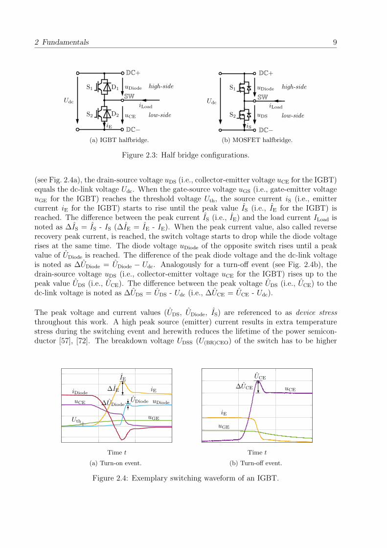
2 Fundamentals 9
uCE
S1 uDiode
S2 low-side
Udc
high-side
iE
D1
D2
DC+
DC−
SWiLoad
(a) IGBT halfbridge.
uDS
S1 uDiode
S2 low-side
Udc
high-side
iS DC−
DC+
SWiLoad
(b) MOSFET halfbridge.
Figure 2.3: Half bridge configurations.
(see Fig. 2.4a), the drain-source voltage uDS (i.e., collector-emitter voltage uCE for the IGBT)equals the dc-link voltage Udc. When the gate-source voltage uGS (i.e., gate-emitter voltageuGE for the IGBT) reaches the threshold voltage Uth, the source current iS (i.e., emittercurrent iE for the IGBT) starts to rise until the peak value IS (i.e., IE for the IGBT) isreached. The difference between the peak current IS (i.e., IE) and the load current ILoad isnoted as ∆IS = IS - IS (∆IE = IE - IE). When the peak current value, also called reverserecovery peak current, is reached, the switch voltage starts to drop while the diode voltagerises at the same time. The diode voltage uDiode of the opposite switch rises until a peakvalue of UDiode is reached. The difference of the peak diode voltage and the dc-link voltageis noted as ∆UDiode = UDiode − Udc. Analogously for a turn-off event (see Fig. 2.4b), thedrain-source voltage uDS (i.e., collector-emitter voltage uCE for the IGBT) rises up to thepeak value UDS (i.e., UCE). The difference between the peak voltage UDS (i.e., UCE) to thedc-link voltage is noted as ∆UDS = UDS - Udc (i.e., ∆UCE = UCE - Udc).
The peak voltage and current values (UDS, UDiode, IS) are referenced to as device stressthroughout this work. A high peak source (emitter) current results in extra temperaturestress during the switching event and herewith reduces the lifetime of the power semicon-ductor [57], [72]. The breakdown voltage UDSS (U(BR)CEO) of the switch has to be higher
iE
uCE
uGE
uDiode
iDiode
UDiode
IE
Time t
∆IE
∆UDiode
Uth
?
6
?6
(a) Turn-on event.
iE
uCE
uGE
UCE
Time t
∆UCE?6
(b) Turn-off event.
Figure 2.4: Exemplary switching waveform of an IGBT.

10 2.1 Power Semiconductor Devices
than the maximum peak voltage UDS to prevent a failure of the semiconductor and thuslimits the device utilization ratio Udc
UDSS( Udc
U(BR)CEO).
2.1.2 Switching Losses
The total losses PLoss of a power semiconductor are traditionally composed of the conductionand switching losses PCond and PSW according to equation (2.2).
PLoss = PCond + PSW (2.2)
Switching losses are appearing because the switching transitions are not happening instan-taneously during the turn-on and -off events. In literature [19], the turn-on losses Eon andturn-off losses Eoff are generally approximated by
Eon =1
2· Udc · ILoad · tOn (2.3)
Eoff =1
2· Udc · ILoad · tOff (2.4)
with a typical turn-on time tOn and turn-off time tOff . However, the switching times varydepending on the dc-link voltage, current, temperature or driver configuration [73], which arenot considered by equation (2.3) or equation (2.4). As the distinction between conductionlosses and switching losses is not very clear, a separation of the measured losses in conductionand switching losses is not trivial.
According to the standard DIN IEC 60747-9 [74], the switching losses of IGBTs are definedusing various threshold levels on the collector-emitter voltage uCE, the emitter current iEand the gate-emitter voltage uGE. However, two major cases are not covered to a sufficientextent. At first, it is not always possible to include a good quality measurement of the gatevoltage in the measurements, which in turn does not allow the determination of the startingor ending of the switching transient. Second, due to fast switching and parasitic inductancein the switching cell, the switching transients include a certain amount of ringing whichvaries from no ringing to several high-frequency oscillations. No information is given in thestandard, on how to determine the starting or ending of a switching transient containingoscillations. Third, the losses of the opposite (free-wheeling) diode are not considered.However, as literature [75] shows, diode turn-off losses do exist and have to be consideredin switching loss measurements.
In this work, the switching losses have to be determined for many different hardware config-urations and operating conditions. Therefore, a universal measurement setup requiring asfew as possible measurement quantities is desirable. The main measurement approaches forthis purpose are documented in literature: double pulse [76], calorimetric [77], [78] and on-line switching loss [79] measurements. The calorimetric measurements require an elaboratetest setup, which is not compatible with big hardware variations and large devices under
2 Fundamentals 11
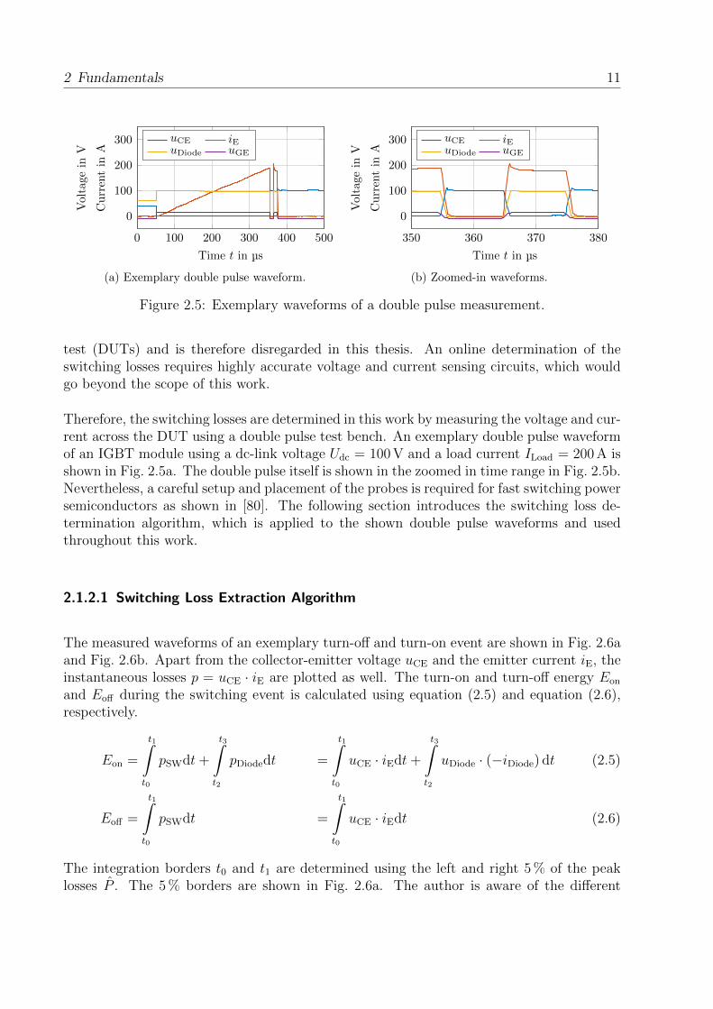
0 100 200 300 400 500
0
100
200
300
Time t in µs
Voltagein
V
Currentin
A
uCE iEuDiode uGE
(a) Exemplary double pulse waveform.
350 360 370 380
0
100
200
300
Time t in µs
Voltagein
V
Currentin
A
uCE iEuDiode uGE
(b) Zoomed-in waveforms.
Figure 2.5: Exemplary waveforms of a double pulse measurement.
test (DUTs) and is therefore disregarded in this thesis. An online determination of theswitching losses requires highly accurate voltage and current sensing circuits, which wouldgo beyond the scope of this work.
Therefore, the switching losses are determined in this work by measuring the voltage and cur-rent across the DUT using a double pulse test bench. An exemplary double pulse waveformof an IGBT module using a dc-link voltage Udc = 100 V and a load current ILoad = 200 A isshown in Fig. 2.5a. The double pulse itself is shown in the zoomed in time range in Fig. 2.5b.Nevertheless, a careful setup and placement of the probes is required for fast switching powersemiconductors as shown in [80]. The following section introduces the switching loss de-termination algorithm, which is applied to the shown double pulse waveforms and usedthroughout this work.
2.1.2.1 Switching Loss Extraction Algorithm
The measured waveforms of an exemplary turn-off and turn-on event are shown in Fig. 2.6aand Fig. 2.6b. Apart from the collector-emitter voltage uCE and the emitter current iE, theinstantaneous losses p = uCE · iE are plotted as well. The turn-on and turn-off energy Eon
and Eoff during the switching event is calculated using equation (2.5) and equation (2.6),respectively.
Eon =
t1ˆ
t0
pSWdt+
t3ˆ
t2
pDiodedt =
t1ˆ
t0
uCE · iEdt+
t3ˆ
t2
uDiode · (−iDiode) dt (2.5)
Eoff =
t1ˆ
t0
pSWdt =
t1ˆ
t0
uCE · iEdt (2.6)
The integration borders t0 and t1 are determined using the left and right 5 % of the peaklosses P . The 5 % borders are shown in Fig. 2.6a. The author is aware of the different

12 2.1 Power Semiconductor Devices
results this method brings comparing to the norm, but as the results are compared amongeach other, only the relative changes are relevant.
The determination of the turn-on losses Eon is made in an analogous way. Although, ad-ditional losses arise due to the reverse recovery effect of the diode. To calculate the diodeturn-off losses, the high-side diode current is required. As the low-side current shunt con-nects the oscilloscope ground to the power ground for the emitter current iE measurement,no additional current shunt can be installed in the high-side path to measure the diodecurrent. In this work, the high-side diode current iDiode is calculated using the inductorcurrent iL and the low-side emitter current iE:
iDiode = iL − iE
The inductor current iL is equal to the emitter current iE imminently before switchingthe switch off at t = tturn−off,− and immediately after turning the switch back on again att = tturn−on,+. A linear interpolation is assumed between these two points.
iL (t = tturn−off) = iE (t = tturn−off,−)
iL (t = tturn−on) = iE (t = tturn−on,+)
An examplary waveform showing the turn-on losses pSW of the switch and the diode losspDiode is shown in Fig. 2.6b. In this work, the term Eon refers to the sum of the turn-onlosses of the switch and turn-off losses of the diode.
Using the double pulse test bench (introduced in section 2.5.3), a large amount of measure-ment waveform data is generated. Due to the large amount, it is not possible to manuallyextract the switching losses of each operating point. Therefore, a MATLAB tool is de-veloped to analyze a large number of measurements and automatically extract the desiredinformation. The details on the operation are found in [82].
P
5% · P
psw
Eoff =´
pswdt
iE
uCE
t0 t1
Time t
(a) Qualitative waveforms of a turn-off event.
pdiode
psw
iE
uCE uDiode
iDiode
Time t
(b) Qualitative waveforms of a turn-on event.
Figure 2.6: Switching events. [81]

2 Fundamentals 13
2.2 Power Semiconductor Gate Drivers
The power semiconductors are turned on and off by applying a certain voltage to thegate-source voltage uGS (MOSFET) or gate-emitter voltage uGE (IGBT). During the op-eration of a power electronic converter, the switches are turned on and off at the switchingfrequency fsw.
A gate drive circuit consists of several major components: an isolated power supply, anisolated signal transceiver, the gate driving amplifier and eventual sensor and protectioncircuits. A generic schematic of a gate drive circuit is plotted in Fig. 2.7. Galvanic isolatedpower supplies are required for the high-side drivers and sometimes, depending on thetopology, also for the low-side drivers. A good overview over existing power supply topologiesfor gate drivers is found in literature [28], [29], [83], [84]
2.2.1 Overview over State of the Art Gate Driving Techniques
An overview over existing gate driver techniques is given in the following. Depending on thepower semiconductor device and switching frequency, different gate driving strategies arerequired. The relevant power semiconductors in this work are Si and SiC MOSFETs andSi IGBTs, which have isolated gate structures. Thus, the main function of the gate driveris to charge and discharge the gate capacitance and not to provide e.g., a pulsed voltageas it is the case for Thyristors [29]. The most commonly used technique is to charge thecapacitor using a voltage source and a series resistance [85], which is henceforth called avoltage source gate driver. Besides a widely used positive supply voltage of Ucc = 15 V tofully turn on a Si power semiconductor, two major turn-off voltage levels do exist [28], [29].
RGLogic inputDC
DC
Gate driverHigh-sideswitch
Low-sideswitch
RGLogic inputDC
DC
Gate driver
GND
Ucc
Figure 2.7: Typical low- and high-side gate driving circuit.

14 2.2 Power Semiconductor Gate Drivers
The positive supply voltage to fully turn on a SiC device is not fixed to 15 V but variesbetween 18 V . . . 25 V, depending on the manufacturer [86]–[89]. Either the gate voltageis tied to Uss = −8 V when using a bipolar supply, or to the ground level Uss = 0 V whenusing a unipolar supply. Bipolar supplies are generally used for IGBTs or SiC MOSFETs incombination with separate turn-on and turn-off gate resistances, whereas unipolar suppliesare mostly used with silicon MOSFETs. A more detailed overview over the differencesbetween Si and SiC devices is found in literature [62], [90]
Apart from voltage source gate drivers, current source gate drivers are used in variousapplications. They use a constant current to charge or discharge the gate capacitance to acertain voltage. Various different current source topologies are well documented in literature[91]–[93]. However, it has been shown, that equal switching performance is achieved whenusing a current source or voltage source gate driver [94].
2.2.2 Silicon MOSFET Gate Drivers
Most converter topologies based on Si MOSFETs employ basic gate driving integratedcircuits (ICs) with a given gate resistance [85]. However, for higher switching frequencyconverters, for example soft switched resonant topologies [95], the losses in the gate drivingcircuit are not negligible anymore. Therefore, full bridge gate drive topologies [96], resonantgate drive topologies [97] or current source gate drivers [92] with gate energy recovery becomea prerequisite. Besides voltage source driven gate drivers, active current source gate driverswith adaptive current levels are introduced in [98], [99].
2.2.3 Silicon IGBT Gate Drivers
Standard IGBT gate drivers for commercial applications are well documented in litera-ture [28], [29]. However, more advanced gate drivers, which aim to influence or controlthe switching transitions, started appearing with the IGBT technology becoming more andmore popular [100]. Soon after, investigations on optimized gate profiles to achieve de-sired switching behavior got published [101]–[106]. Most investigations are dealing withhigh-power IGBTs [107], [108] because low-power devices show shorter switching times andhence, require faster timing actions of the active gate drive unit. Besides discrete stage-wisedrivers [109], [110], active control of the voltage and current slopes of high-power IGBTmodules is available [111]–[113]. Although the active control of the switching transients iscurrently only feasible using high-power modules, where the bandwidth of the control loopis within an acceptable range. Literature shows, that the switching transients for modernlow-voltage power devices, especially for mobile applications, are influenced actively usingvoltage source stage-wise drivers [114]–[117] or current source stage-wise driver topologies[118], [119] including the active limitation of the voltage slope. To reduce part count and
2 Fundamentals 15
costs of the active drivers, IC or application-specific integrated circuit (ASIC) solutions havebeen demonstrated [108], [110].
2.2.4 Silicon Carbide MOSFET Gate Drivers
With the WBG device technology becoming mature [38], investigations on respective gatedrivers are arising [120]–[122]. The SiC technology is an option to replace Si IGBT powerdevices. Comparisons between both technologies are covered in literature [40], [123], [124].Due to the significantly increased switching speed of SiC devices [125], protection of thelater becomes more challenging. Possible solutions for overcurrent and overtemperatureprotection for SiC devices are shown in [126], [127]. Analogously to the various differentSi MOSFET and IGBT driver topologies, current source drivers as well as resonant driversgot investigated for SiC devices as well [91], [93], [128]. To reach higher dc-link voltages,either medium-voltage power devices, or a series connection of multiple low-voltage devicescan be used. However, due to the high switching speed, it is challenging to guarantee anequal voltage sharing on the devices during the switching transients [129]–[131], whereasmedium-voltage gate drivers have high demands on isolated power supplies [84], [132]–[134].
To influence the switching behavior of SiC MOSFETs, various different active gate driverapproaches were investigated. For example, a boosting capacitor is connected to the gateduring the switching transient to boost the gate current [135]–[137] or the Kelvin sourcepotential is connected to different voltage levels [138] to influence the gate current. Anotherexample is shown in [139], where the gate resistor is bypassed to boost the gate current.These basic active drivers show, that an influence on the transients is possible and a positiveeffect on the EMI, switching losses, overvoltage or overcurrent is possible. However, thedegree of freedom is very limited as only a single passive device (e.g., boosting capacitor) isdimensioned for the worst case operating point or only a single additional switching actionduring the switching transient is possible.
Active gate drivers with more stages of freedom are presented in [140]–[142], which makeuse of switched resistor topologies. The control of the different stages during the switchingtransient is made using complex programmable logic devices (CPLDs), with feedback loopsusing different voltage and current levels of the DUT. However, the feedback loop constitutesthe bottleneck regarding increased switching speed, which is in the range of 10 V/ns in theshown publication [142]. Furthermore, the opposite free-wheeling diode voltage is neglectedin the investigations, which have been shown to reach high overshoots at fast switchingtransients [143].

16 2.3 Power Semiconductor Packaging
(a) DirectFET™.
(b) TO-247.(c) SOT-227-4.
Figure 2.8: Different power semiconductor packages.
2.3 Power Semiconductor Packaging
Power electronic switches require a housing to allow an easy thermal and electrical connec-tivity, which can be handled using basic manufacturing tools such as soldering or screwing[30]. Furthermore, the package keeps humidity and dust away. Besides embedded solu-tions [32], [144], various different package solutions do exist for discrete devices. A fewexamples are given in Fig. 2.8. The shown DirectFET™ package (see Fig. 2.8a) uses directsolder interconnections for the top-side copper case connection and solder bumps on thebottom-side for soldering directly on a PCB, allowing double sided cooling and electricalconnection [145]. The shown remaining packages are designed using a direct bonded copper(DBC) substrate which is enclosed in a plastic mold. Figure 2.9 shows the structure of atypical power package. The DBC substrate usually consists of two copper layers with anelectrical isolation layer in the middle. For most Si based power semiconductors Aluminumoxide (Alumina, Al2O3) is used, whereas for most SiC based semiconductors, Aluminumnitride (AlN) is used due to a higher thermal conductivity. The bottom-side copper layer isthermally connected to the heat sink via thermal interface material (TIM) [146] to ensure agood thermal conductance. Various die attach solutions are available for electrical contact-ing the top-side of the bare die [41], [147]. Bond wires are widely spread and used in mostcommercially available power modules. A Kulicke & Soffa Model 4123 wire wedge bonderis used in this work to attach bare dies. The bare die bottom-side is attached on the topcopper layer of the DBC substrate.
Heat sink
Bare die
Bond wires
Copper layer
Isolation layer
Copper layer
Plastic case
TIM
Figure 2.9: Side cut through a power package.
2 Fundamentals 17
2.3.1 Parasitic Elements Extraction
The electrical design of the switching cell has a direct impact on the transient switchingbehavior due to addition of parasitic elements, such as inductive or capacitive components.The parasitic elements are due to the mechanical and thermal design of the power module.A compromise between optimal electrical, mechanical and thermal design has to be made.Various works are investigating on the extraction of the different parasitic elements fromexisting power modules [148], [149].
While the extraction of capacitive elements is quite simple, as it will be shown in section 3.4,two different kinds of parasitic inductive elements are considered: closed loop and partialinductances. The extraction of the latter is not simple due to the mutual coupling effectsas described in [150]. Different methods employing for example time domain reflectometry[151] or impedance measurements [152] to extract the inductance of complex module designs,and thus consider mutual coupling effects, are investigated in literature. However, thesemethods must be very specifically adapted to the power module under investigation and arenot necessarily applicable to every configuration. The estimation of the inductance of bondwires is covered in [153], [154]. Besides the parasitic inductance, the resistance of the leadwires [155] or the determination of gate resistance using scattering parameters [156] is ofinterest. While these methods provide good results for certain parasitic inductive elements,not every partial inductance can be determined.
2.3.2 Influence on the Switching Transients
It is known, that the design of the switching cell has a non-negligible effect on the switchingtransients [50], [51], [157]–[159]. Therefore, several investigations have been made to quantifythe effects of the parasitic elements on the switching behavior [47]–[49]. Besides the effect onthe switching transients themselves, the effects on the system level have been investigatedin [50]. A good design of the switching cell is required for example for paralleling powersemiconductor dies in power packages to ensure equal load sharing during the switchingtransients. This is covered widely in literature [160]–[162] for Si IGBTs and is even morecritical for WBG power semiconductors [163]. The impact of parasitic influence on theswitching transients of SiC MOSFETs is investigated in detail in [164]. Especially, thequasi soft turn-on behavior, which is discussed in detail in chapter 4, is mentioned inhereas almost zero voltage switching. Intensive research work is happening to reduce the strayinductances of power modules, which leads to new manufacturing or assembly concepts suchas three dimensional (3D) stacked power modules [165], using the flip chip technology [166]allowing double sided cooling [167], using a low inductive two layer flexible PCB for dc-linkinterconnection [168] and others [169]–[171].
Besides experimental demonstrators of low inductive power modules, the extracted parasiticelements can be used to conduct simulations of the transient switching events in the time

18 2.4 Finite Element Method
domain. A detailed investigation is shown in [172] for a TO-247 package. A detailed analysiswith massive parameter variations using a single setup is not available in literature.
2.4 Finite Element Method
A numerical method to solve differential equations for geometric bodies of any type ofshape is the so-called finite element method (FEM). The two dimensional (2D) or 3D spaceis partitioned in many small geometric bodies, usually in a triangular or tetrahedral shape.Inside this partitioned body, the differential equations are solved according to the boundaryconditions of the finite element. A detailed introduction of the theoretical background isfound in [173].
For the understanding of the finite element (FE) simulations conducted in this work, onlythe principle of operation and a certain number of material parameters are required. Thefollowing subsection gives a brief overview over the employed material parameters.
2.4.1 Material Parameters
Accurate material parameters are crucial to achieve reasonable simulation results. Therefore,all material parameters used in simulations in this work are taken from [31] and listed inTable 2.1. The specific conductivity of the insulating materials is chosen to 1 S/m to achievea better convergence of the simulations. This is valid because the voltages occurring in thesimulations are in the range of 0 V . . . 10 V. The influence on the simulations is neglected asthe specific conductivity of the conducting materials is higher by several orders of magnitude.The value for Aluminum oxide (Alumina) is found by comparing different simulations resultsto measurements. A value for silicone gel is not available in the data sheets. Therefore,simulations in the range of 2.8 (silicone varnish) and 3.6 (silicone rubber) are carried out.The influence of the silicone gel in power modules is shown in section 3.4.2.
Table 2.1: Material parameters used in simulations
Material σr εr µr
Copper (Cu) 5.7× 10⁷ Sm 1 1
Aluminum (Al) 3.7× 10⁷ Sm 1 1
Alumina (Al2O3) 1 Sm 11.5 1
Aluminum Nitride (AlN) 1 Sm 9 1
Vacuum 1 Sm 1 1
Silicone gel 1 Sm 2.8 . . . 3.6 1

2 Fundamentals 19
2.5 Measurement Equipment and Tools
Every measurement probe or tool transforms a measured quantity using a certain distur-bance into an user readable format. A wide range of different disturbances do exist, forexample distortion, delay time, noise or quantization error. In this work, especially thedelay times of voltage and current probes are crucial to guarantee accurate measurements.Besides a detailed analysis of the employed measurement probes, the major equipment andtools used in this work are introduced in this section.
2.5.1 Current Pulse Generator
Analogous to the voltage step response analysis of voltage probes, a current pulse is usedto analyze the dynamic behavior of current probes [174]. However, in this thesis, the usageof the current pulse generator is different from its main application, which was intended toevaluate the bandwidth of various current probing devices. Instead, it is used to determinepartial inductances between two given terminals of a given electrical path. The schematicand a photograph of the current pulse generator is shown in Fig. 2.10.
The goal is to determine the inductance value of the unknown inductance LDUT with aresistive component Rσ. The switches S1 and S2 are closed to magnetize the inductance L1
to the desired current level. After reaching the desired current level, the switch S1 is openedand diode D goes into freewheeling state. After opening the switch S2, the current is forcedto commutate into LDUT. The high current slopes allow a determination of the inductancein the single nano-henry range. The energy stored in L1 is below the maximum supportableavalanche energy [175], [176] of the switch S2. The unknown inductance LDUT is determinedby measuring the current iL and the voltage drop uL. The procedure is further explained insection 3.3.2.
Udc
R
L1
LDUT
uL
S1
S2D
iL
Rσ
(a) Topology.
L1
LDUT
uLS1
S2
(b) Photograph. [174]
Figure 2.10: Current pulse generator.
20 2.5 Measurement Equipment and Tools
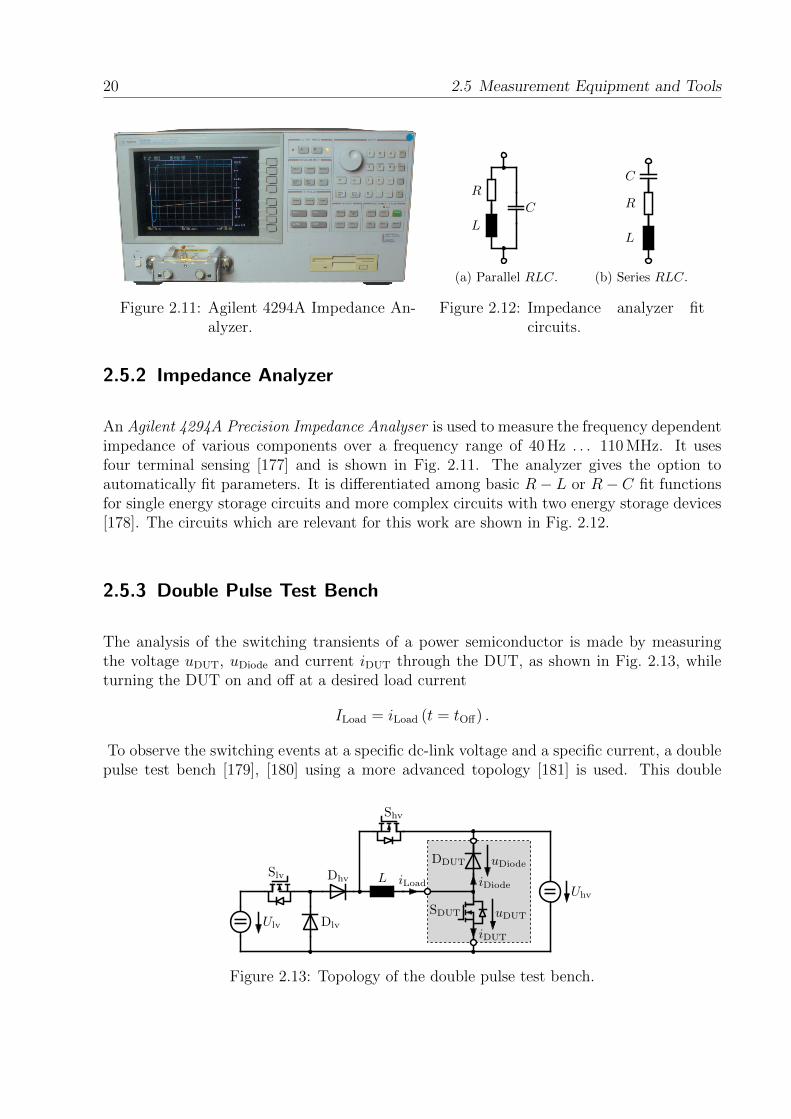
Figure 2.11: Agilent 4294A Impedance An-alyzer.
R
L
C
(a) Parallel RLC.
R
L
C
(b) Series RLC.
Figure 2.12: Impedance analyzer fitcircuits.
2.5.2 Impedance Analyzer
An Agilent 4294A Precision Impedance Analyser is used to measure the frequency dependentimpedance of various components over a frequency range of 40 Hz . . . 110 MHz. It usesfour terminal sensing [177] and is shown in Fig. 2.11. The analyzer gives the option toautomatically fit parameters. It is differentiated among basic R− L or R− C fit functionsfor single energy storage circuits and more complex circuits with two energy storage devices[178]. The circuits which are relevant for this work are shown in Fig. 2.12.
2.5.3 Double Pulse Test Bench
The analysis of the switching transients of a power semiconductor is made by measuringthe voltage uDUT, uDiode and current iDUT through the DUT, as shown in Fig. 2.13, whileturning the DUT on and off at a desired load current
ILoad = iLoad (t = tOff) .
To observe the switching events at a specific dc-link voltage and a specific current, a doublepulse test bench [179], [180] using a more advanced topology [181] is used. This double
uDUTSDUT
DDUT
iLoad
Ulv
Uhv
Dlv
Dhv
Shv
LSlviDiode
iDUT
uDiode
Figure 2.13: Topology of the double pulse test bench.

2 Fundamentals 21
TEC unit
Control unit
Figure 2.14: Photograph of the temperature unit. [82]
pulse test bench allows setting the desired current level ILoad independently of the dc-linkvoltage Uhv. The load current is set by the Ulv voltage source and the on-time of the DUT.Furthermore, the test bench allows automated series tests to sweep through the parametersof voltage, current and temperature. Currents and voltages in the range of 0 A . . . 1000 Aand 0 V . . . 1000 V are configurable, while temperatures are set to any desired value between−40 C . . . 200 C. The temperature control system is further deployed in section 2.5.4. Thistest bench is used for all double pulse measurements throughout this thesis.
2.5.4 Temperature System
To conduct measurements at defined case or junction temperatures, the temperature controlunit as presented in [82], [182] is used. The temperature unit allows to set the case tempera-ture of a given power module to a given temperature in the range of −40 C . . . 200 C usingthermoelectric coolers (TECs). The instrument has a communication interface to the dou-ble pulse test bench and thus enables double pulse measurements at different temperaturesweeps. A photograph of the setup is shown in Fig. 2.14.
2.5.5 Voltage and Current Probes
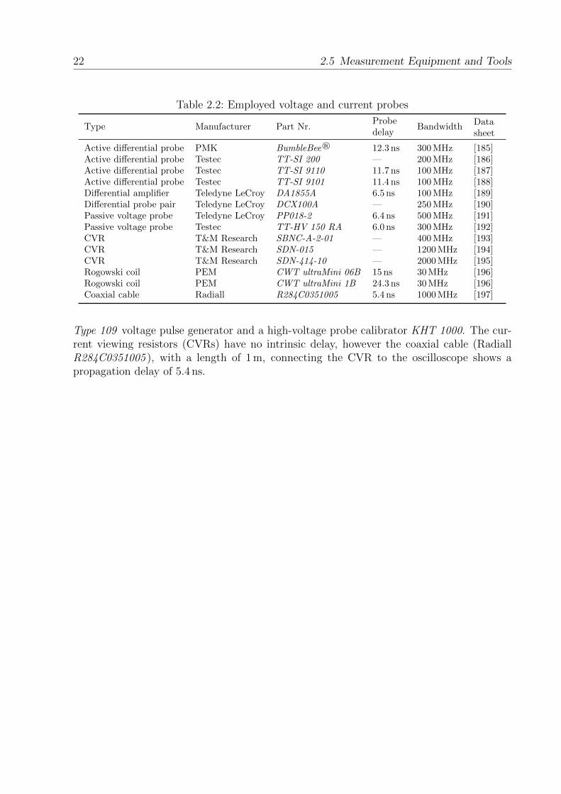
Accurate measurements using WBG power semiconductors require not only high-end probes,but also their correct use [183]. Different publications on this topic are available [80], [184].Various measurement probes are used to measure current or voltages throughout this work.An overview of the employed probes is listed in Table 2.2. A key property of each probe,which is not always listed in the data sheet, is the delay time. Especially regarding theswitching times of SiC MOSFETs, the probe delay times are a critical parameter as thedelays are within the range of the switching times of the devices. It is crucial for the eval-uation of the measurements to have synchronized current and voltage measurements. Theindicated delay times are determined using a measurement setup consisting of a Tektronix
22 2.5 Measurement Equipment and Tools
Table 2.2: Employed voltage and current probes
Type Manufacturer Part Nr.Probedelay
BandwidthDatasheet
Active differential probe PMK BumbleBee® 12.3 ns 300 MHz [185]Active differential probe Testec TT-SI 200 — 200 MHz [186]Active differential probe Testec TT-SI 9110 11.7 ns 100 MHz [187]Active differential probe Testec TT-SI 9101 11.4 ns 100 MHz [188]Differential amplifier Teledyne LeCroy DA1855A 6.5 ns 100 MHz [189]Differential probe pair Teledyne LeCroy DCX100A — 250 MHz [190]Passive voltage probe Teledyne LeCroy PP018-2 6.4 ns 500 MHz [191]Passive voltage probe Testec TT-HV 150 RA 6.0 ns 300 MHz [192]CVR T&M Research SBNC-A-2-01 — 400 MHz [193]CVR T&M Research SDN-015 — 1200 MHz [194]CVR T&M Research SDN-414-10 — 2000 MHz [195]Rogowski coil PEM CWT ultraMini 06B 15 ns 30 MHz [196]Rogowski coil PEM CWT ultraMini 1B 24.3 ns 30 MHz [196]Coaxial cable Radiall R284C0351005 5.4 ns 1000 MHz [197]
Type 109 voltage pulse generator and a high-voltage probe calibrator KHT 1000. The cur-rent viewing resistors (CVRs) have no intrinsic delay, however the coaxial cable (RadiallR284C0351005 ), with a length of 1 m, connecting the CVR to the oscilloscope shows apropagation delay of 5.4 ns.

3 Methodology on Power SemiconductorPackage Parasitics Extraction
This chapter describes the employed and developed methodologies to extract the electricalparasitic elements from various power semiconductor packages. The investigation is focusedon parasitic capacitances and inductances. While the capacitive elements are more trivial toextract due to the generally planar structures of the power packages, the inductive elementsrequire a higher effort.
Simulative and experimental approaches are shown for both, the capacitive and inductiveparasitic element extraction. The parasitic inductive element investigation is split into closedloop inductances and partial inductances. The determination of partial inductances is morechallenging, therefore an experimental approach using a current pulse generator and doublepulse tests is developed and introduced. The various different approaches are applied on twopower semiconductor devices: a three-phase IGBT power module and a discrete MOSFETin a TO-247 package. It is shown, that, depending on the package, switching cell geometryand the voltage and current sensing abilities, several methods are required to fully determineall parasitic elements of a given power device.
Using the found parasitic elements, a model of the IGBT power module is created and thesimulated switching behavior is compared to double pulse measurements. A good matchbetween the simulated and measured waveforms is found, which reinforces the developedmethodology and the determined parasitic element values.
3.1 Scope of the Investigation
Prior to the presentation of the developed methodology, the scope of the relevant parasiticelements is defined. Capacitive and inductive elements are subject to investigation in thiswork. Figure 3.1 shows a switching cell of a half bridge including the relevant parasiticelements: the low- and high-side collector and emitter inductances LC,L, LC,H, LE,L, LE,H
in the IGBT path, the low- and high-side inductances LD,L, LD,H in the diode path andthe capacitance CSW between the jumping potential (SW) and the heat sink (GND). Solelythe parasitic elements created by the package are relevant to the conducted investigations.The parasitic elements contributed by the power semiconductors themselves, such as thegate-source capacitance CGS, the gate-drain capacitance CGD or the drain-source capacitance
23

24 3.2 Simulative Parasitic Elements Extraction
Power Module
SW
DC−
Udc
uGE,H
uGE,L
DC+
LD,H
Lσ,DC/2
Lσ,DC/2
LD,L
LG,LS
LG,HS
LC,H
LE,H
LC,L
LE,L
SemiconductorBare Die
CSW
CGC
CGE
CCERG,int
Figure 3.1: Parasitic inductances in a half bridge.
CDS, are not considered. A simulative and experimental approach to extract both, theparasitic capacitances and inductances, are presented and discussed in the following sections.The experimental verification of the presented methodology is carried out using two casestudies: a detailed investigation on the HybridPACK™2 and on a SiC MOSFET in a TO-247package.
3.2 Simulative Parasitic Elements Extraction
The goal of the simulative approach is to extract the parasitic elements of a given packageusing the 3D computer aided design (CAD) data. As such, it is possible to estimate theparasitic elements and evaluate the influence on the switching behavior (see section 3.6)prior to manufacturing the package. The theoretical determination of the parasitic elementsis made using FEM (see section 2.4). The simulation software COMSOL Multiphysics andANSYS Maxwell are used.
3.2.1 Capacitive Elements
In power modules, the capacitive coupling between the different layers of the DBC substrateis of interest. The geometry of DBC substrates usually form a parallel-plate capacitor of

3 Methodology on Power Semiconductor Package Parasitics Extraction 25
which the capacitance value C is easily determined by
C =εA
d
with the surface area A, distance d between both layers and ε the dielectric constant of theinsulating material. Commercially available DBC substrates consist of an Alumina (Al2O3)isolation barrier with a typical thickness d = 300 µm [198]. Commercial power packagesare covered with a silicone gel to prevent dirt and humidity from reducing the blockingcapability of the power semiconductors. Therefore, FE simulations are used instead ofthe parallel-plate model to consider the stray fields inside the silicone gel, whose dielectricconstant is different from vacuum (or air).
3.2.2 Inductive Elements
The inductance is extracted from the CAD models of the DBC substrate using FE simulationsoftware. A test current is injected into a given circuit loop which is the source for anelectric and magnetic field ~H and ~B. The fundamentals on magnetic components are welldocumented in literature [199], [200]. The energy Wmag stored in the electromagnetic fieldis given by equation (3.1). Using the energy WL stored in an inductor L according toequation (3.2), the inductance L is extracted according to equation (3.3).
Wmag =1
2
˚
V
~B · ~H dV (3.1)
WL = Wmag =1
2LI2 (3.2)
L =
˚
V
~B · ~H dV
I2 (3.3)
3.3 Experimental Parasitic Elements ExtractionMethodology
Besides determining the parasitic inductances or capacitances using simulations, experi-mental verification is envisaged. Different methodologies are presented in the following andverified in two application examples consisting of a three-phase power module and a discretepower semiconductor.

26 3.3 Experimental Parasitic Elements Extraction Methodology
iL Rσ
uL
Figure 3.2: Partial inductance including resistive part.
3.3.1 Capacitance and Closed Loop Inductance Determination
The values of capacitive and closed loop inductive elements are extracted from impedancemeasurements. A frequency dependent impedance of an electric circuit with passive com-ponents is measured and the values of the passive components is determined using differentfitting functions. An Agilent 4294A Precision Impedance Analyser is used for measurementsin the frequency range f = 40 Hz . . . 110 MHz (see section 2.5.2).
3.3.2 Partial Inductance Determination
A partial inductance is defined in this work as the inductance between two measurementpoints on a given path, which is traversed by a current i [150]–[152]. The voltage dropacross a partial inductance L including a resistive part Rσ while conducting the current i,as shown in Fig. 3.2, is given by equation (3.4).
uL = Rσ · i+ Ldi
dt(3.4)
The unknown parameters Rσ and L are found by fitting the measured voltage uMeas to thecalculated voltage uL from the measured current i using the least-squares regression method[201]. An exemplary extraction is shown using the measured current i and measured voltageuMeas, which are plotted in Fig. 3.3. It is seen, that the calculated voltage uL using the fittedparameters L = 101.3 nH and Rσ = 423 mΩ matches the measured voltage uMeas.
To increase the accuracy of the fitting parameters, a steep current slope is required duringthe measurement. In this work, two methodologies to generate a steep current slope are
−0.4−0.2 0 0.2 0.4 0.6 0.8 1 1.2 1.4−5
0
5
10
15
Time in µs
iin
A
uLin
V
iuMeas
uL = Rσ · i+ Ldidt
Figure 3.3: Exemplary waveforms of a partial inductance measurement.

3 Methodology on Power Semiconductor Package Parasitics Extraction 27
employed: a current pulse generator and a switching transient of a power semiconductor.
The current pulse generator, as introduced in section 2.5.1, requires a high bandwidthcurrent measurement, such as for example a CVR. However, introducing a CVR into acurrent path requires a mechanical and electrical modification of the circuit, which is notalways possible or wanted. Therefore, an alternative is to use the slope of the emittercurrent of the IGBT during a switching transient. As the emitter current iE during aswitching transient is less steep compared to the current pulse generator current, a currentmeasurement probe with a lower bandwidth is sufficient. In this case, the use of Rogowskicoils is possible, which allows to measure the current without altering the electric circuit.
3.4 Application Example 1: Infineon HybridPACK™2
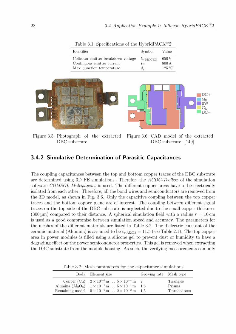
The effectiveness of the introduced simulation and measuring techniques is shown using anInfineon HybridPACK™2 IGBT power module [202], as pictured in Fig. 3.4. The positive andnegative dc-link terminals DC+ and DC− and the ac output SW terminals are indicated.The low- and high-side gate contacting pins are indicated using GL and GH. The three halfbridges are labeled using the letters A, B and C. The specifications are listed in Table 3.1.
3.4.1 3D Model of the Direct Bonded Copper Substrate
As a basis for the FE simulations, a CAD model of the DBC substrate is developed. Therefor,a single half-bridge, as shown in Fig. 3.5, is extracted of the HybridPACK™2 power module.Out of the extracted DBC substrate, a CAD model is created, as pictured in Fig. 3.6. Athickness of 300 µm is determined for the isolating ceramic and for both copper layers.
SW SW SW
DC+DC−
GL
GH
based on photo DSC09475-scaled-rotated
A B C
DC+DC−DC+DC−
Figure 3.4: Photograph of the HybridPACK™2. [149]
28 3.4 Application Example 1: Infineon HybridPACK™2
Table 3.1: Specifications of the HybridPACK™2
Identifier Symbol Value
Collector-emitter breakdown voltage U(BR)CEO 650 VContinuous emitter current IE 800 AMax. junction temperature ϑj 125 C
Figure 3.5: Photograph of the extractedDBC substrate.
DC+GH
SWGL
DC−
Figure 3.6: CAD model of the extractedDBC substrate. [149]
3.4.2 Simulative Determination of Parasitic Capacitances
The coupling capacitances between the top and bottom copper traces of the DBC substrateare determined using 3D FE simulations. Therefor, the ACDC-Toolbox of the simulationsoftware COMSOL Multiphysics is used. The different copper areas have to be electricallyisolated from each other. Therefore, all the bond wires and semiconductors are removed fromthe 3D model, as shown in Fig. 3.6. Only the capacitive coupling between the top coppertraces and the bottom copper plane are of interest. The coupling between different signaltraces on the top side of the DBC substrate is neglected due to the small copper thickness(300 µm) compared to their distance. A spherical simulation field with a radius r = 10 cmis used as a good compromise between simulation speed and accuracy. The parameters forthe meshes of the different materials are listed in Table 3.2. The dielectric constant of theceramic material (Alumina) is assumed to be εr,Al2O3 = 11.5 (see Table 2.1). The top copperarea in power modules is filled using a silicone gel to prevent dust or humidity to have adegrading effect on the power semiconductor properties. This gel is removed when extractingthe DBC substrate from the module housing. As such, the verifying measurements can only
Table 3.2: Mesh parameters for the capacitance simulations
Body Element size Growing rate Mesh type
Copper (Cu) 2× 10⁻⁴ m . . . 5× 10⁻⁴ m 2 TrianglesAlumina (Al2O3) 1× 10⁻⁴ m . . . 5× 10⁻⁴ m 1.5 PrismsRemaining model 5× 10⁻⁴ m . . . 2× 10⁻² m 1.5 Tetrahedrons
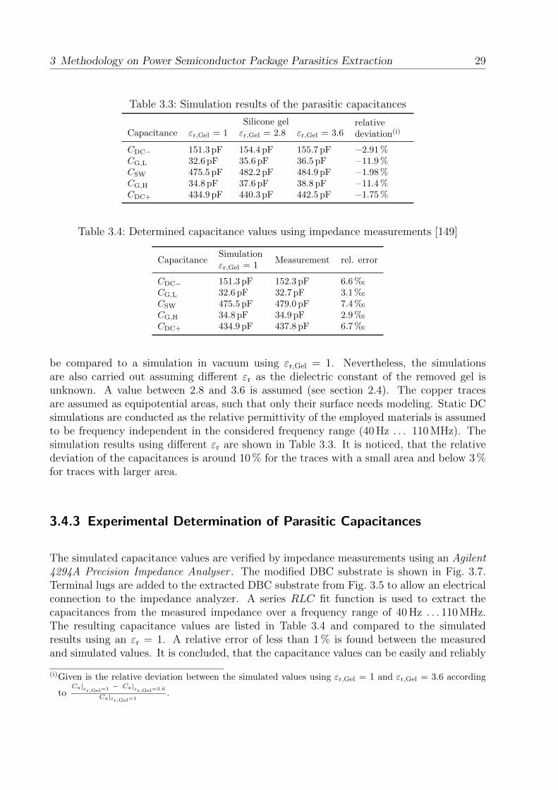
3 Methodology on Power Semiconductor Package Parasitics Extraction 29
Table 3.3: Simulation results of the parasitic capacitances
Silicone gel relativedeviation(i)Capacitance εr,Gel = 1 εr,Gel = 2.8 εr,Gel = 3.6
CDC− 151.3 pF 154.4 pF 155.7 pF −2.91 %CG,L 32.6 pF 35.6 pF 36.5 pF −11.9 %CSW 475.5 pF 482.2 pF 484.9 pF −1.98 %CG,H 34.8 pF 37.6 pF 38.8 pF −11.4 %CDC+ 434.9 pF 440.3 pF 442.5 pF −1.75 %
Table 3.4: Determined capacitance values using impedance measurements [149]
CapacitanceSimulationεr,Gel = 1
Measurement rel. error
CDC− 151.3 pF 152.3 pF 6.6 ‰CG,L 32.6 pF 32.7 pF 3.1 ‰CSW 475.5 pF 479.0 pF 7.4 ‰CG,H 34.8 pF 34.9 pF 2.9 ‰CDC+ 434.9 pF 437.8 pF 6.7 ‰
be compared to a simulation in vacuum using εr,Gel = 1. Nevertheless, the simulationsare also carried out assuming different εr as the dielectric constant of the removed gel isunknown. A value between 2.8 and 3.6 is assumed (see section 2.4). The copper tracesare assumed as equipotential areas, such that only their surface needs modeling. Static DCsimulations are conducted as the relative permittivity of the employed materials is assumedto be frequency independent in the considered frequency range (40 Hz . . . 110 MHz). Thesimulation results using different εr are shown in Table 3.3. It is noticed, that the relativedeviation of the capacitances is around 10 % for the traces with a small area and below 3 %for traces with larger area.
3.4.3 Experimental Determination of Parasitic Capacitances
The simulated capacitance values are verified by impedance measurements using an Agilent4294A Precision Impedance Analyser . The modified DBC substrate is shown in Fig. 3.7.Terminal lugs are added to the extracted DBC substrate from Fig. 3.5 to allow an electricalconnection to the impedance analyzer. A series RLC fit function is used to extract thecapacitances from the measured impedance over a frequency range of 40 Hz . . . 110 MHz.The resulting capacitance values are listed in Table 3.4 and compared to the simulatedresults using an εr = 1. A relative error of less than 1 % is found between the measuredand simulated values. It is concluded, that the capacitance values can be easily and reliably
(i)Given is the relative deviation between the simulated values using εr,Gel = 1 and εr,Gel = 3.6 according
toCx|εr,Gel=1 − Cx|εr,Gel=3.6
Cx|εr,Gel=1.
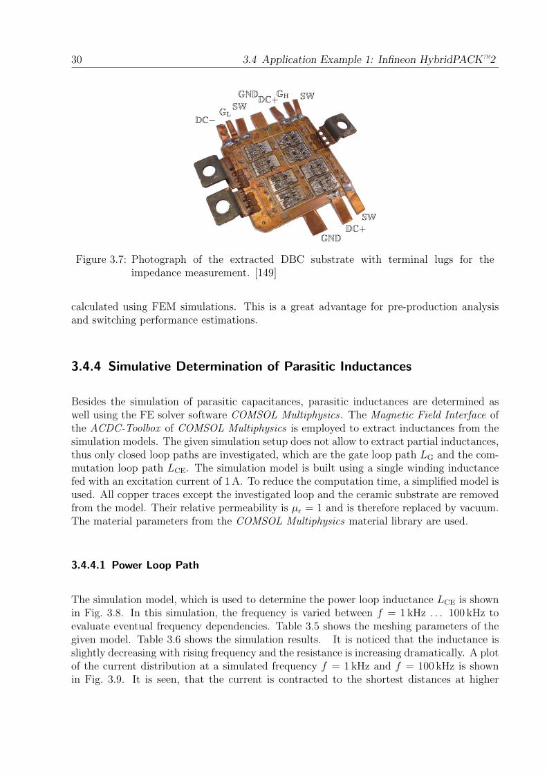
30 3.4 Application Example 1: Infineon HybridPACK™2
DC−GL
SWGNDDC+GH SW
SWDC+
GND
Figure 3.7: Photograph of the extracted DBC substrate with terminal lugs for theimpedance measurement. [149]
calculated using FEM simulations. This is a great advantage for pre-production analysisand switching performance estimations.
3.4.4 Simulative Determination of Parasitic Inductances
Besides the simulation of parasitic capacitances, parasitic inductances are determined aswell using the FE solver software COMSOL Multiphysics . The Magnetic Field Interface ofthe ACDC-Toolbox of COMSOL Multiphysics is employed to extract inductances from thesimulation models. The given simulation setup does not allow to extract partial inductances,thus only closed loop paths are investigated, which are the gate loop path LG and the com-mutation loop path LCE. The simulation model is built using a single winding inductancefed with an excitation current of 1 A. To reduce the computation time, a simplified model isused. All copper traces except the investigated loop and the ceramic substrate are removedfrom the model. Their relative permeability is µr = 1 and is therefore replaced by vacuum.The material parameters from the COMSOL Multiphysics material library are used.
3.4.4.1 Power Loop Path
The simulation model, which is used to determine the power loop inductance LCE is shownin Fig. 3.8. In this simulation, the frequency is varied between f = 1 kHz . . . 100 kHz toevaluate eventual frequency dependencies. Table 3.5 shows the meshing parameters of thegiven model. Table 3.6 shows the simulation results. It is noticed that the inductance isslightly decreasing with rising frequency and the resistance is increasing dramatically. A plotof the current distribution at a simulated frequency f = 1 kHz and f = 100 kHz is shownin Fig. 3.9. It is seen, that the current is contracted to the shortest distances at higher
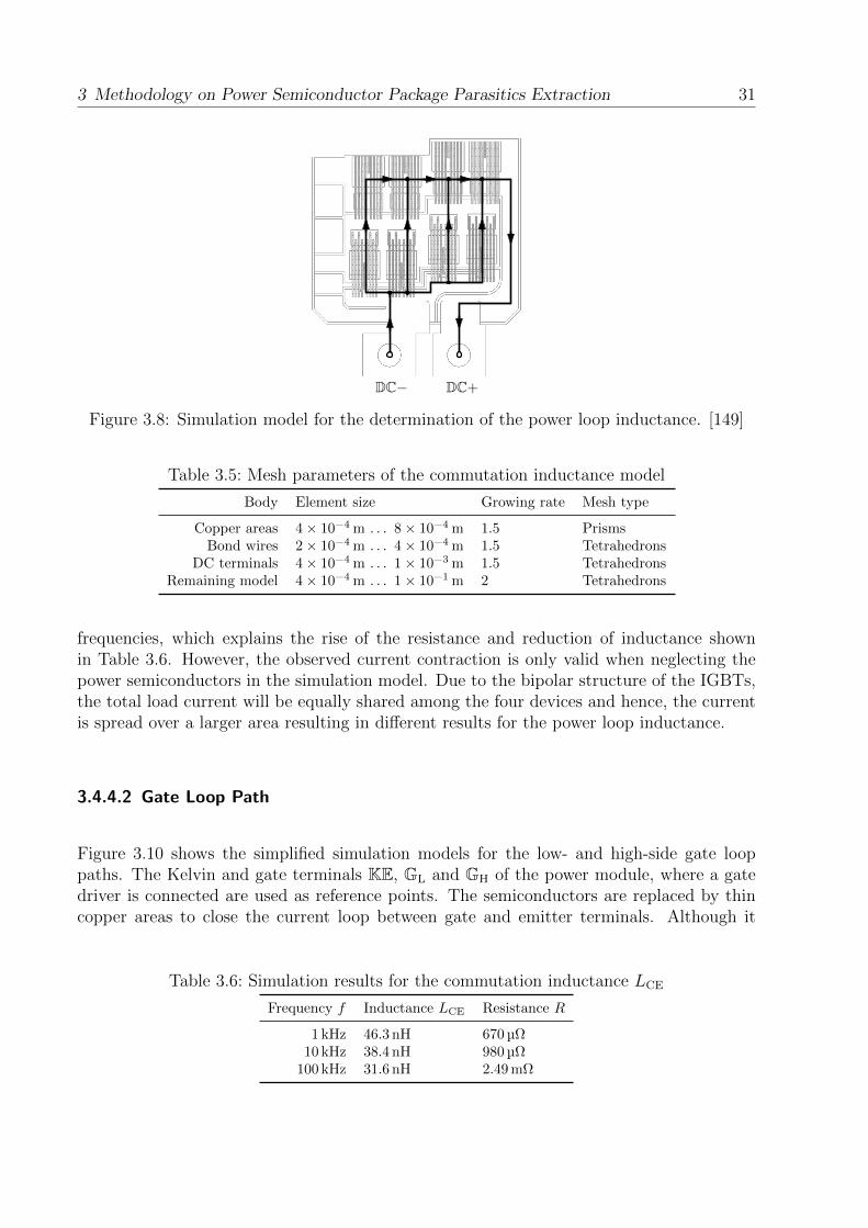
3 Methodology on Power Semiconductor Package Parasitics Extraction 31
DC− DC+
Figure 3.8: Simulation model for the determination of the power loop inductance. [149]
Table 3.5: Mesh parameters of the commutation inductance model
Body Element size Growing rate Mesh type
Copper areas 4× 10⁻⁴ m . . . 8× 10⁻⁴ m 1.5 PrismsBond wires 2× 10⁻⁴ m . . . 4× 10⁻⁴ m 1.5 Tetrahedrons
DC terminals 4× 10⁻⁴ m . . . 1× 10⁻³ m 1.5 TetrahedronsRemaining model 4× 10⁻⁴ m . . . 1× 10⁻¹ m 2 Tetrahedrons
frequencies, which explains the rise of the resistance and reduction of inductance shownin Table 3.6. However, the observed current contraction is only valid when neglecting thepower semiconductors in the simulation model. Due to the bipolar structure of the IGBTs,the total load current will be equally shared among the four devices and hence, the currentis spread over a larger area resulting in different results for the power loop inductance.
3.4.4.2 Gate Loop Path
Figure 3.10 shows the simplified simulation models for the low- and high-side gate looppaths. The Kelvin and gate terminals KE, GL and GH of the power module, where a gatedriver is connected are used as reference points. The semiconductors are replaced by thincopper areas to close the current loop between gate and emitter terminals. Although it
Table 3.6: Simulation results for the commutation inductance LCE
Frequency f Inductance LCE Resistance R
1 kHz 46.3 nH 670 µΩ10 kHz 38.4 nH 980 µΩ
100 kHz 31.6 nH 2.49 mΩ
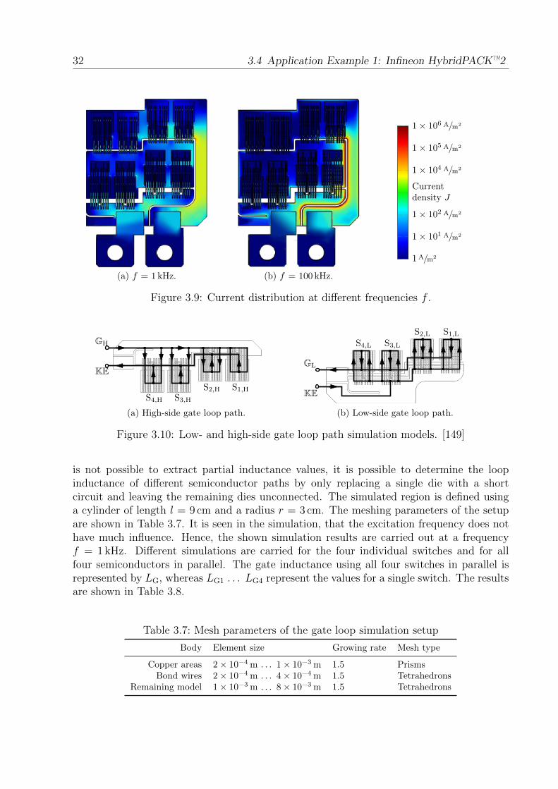
32 3.4 Application Example 1: Infineon HybridPACK™2
(a) f = 1 kHz. (b) f = 100 kHz.
1A/m2
1× 101 A/m2
1× 10² A/m2
Currentdensity J
1× 10⁴ A/m2
1× 10⁵ A/m2
1× 10⁶ A/m2
Figure 3.9: Current distribution at different frequencies f .
S4,H S3,H
S2,H S1,H
KE
GH
(a) High-side gate loop path.
S4,L S3,L
S2,L S1,L
KE
GL
(b) Low-side gate loop path.
Figure 3.10: Low- and high-side gate loop path simulation models. [149]
is not possible to extract partial inductance values, it is possible to determine the loopinductance of different semiconductor paths by only replacing a single die with a shortcircuit and leaving the remaining dies unconnected. The simulated region is defined usinga cylinder of length l = 9 cm and a radius r = 3 cm. The meshing parameters of the setupare shown in Table 3.7. It is seen in the simulation, that the excitation frequency does nothave much influence. Hence, the shown simulation results are carried out at a frequencyf = 1 kHz. Different simulations are carried for the four individual switches and for allfour semiconductors in parallel. The gate inductance using all four switches in parallel isrepresented by LG, whereas LG1 . . . LG4 represent the values for a single switch. The resultsare shown in Table 3.8.
Table 3.7: Mesh parameters of the gate loop simulation setup
Body Element size Growing rate Mesh type
Copper areas 2× 10⁻⁴ m . . . 1× 10⁻³ m 1.5 PrismsBond wires 2× 10⁻⁴ m . . . 4× 10⁻⁴ m 1.5 Tetrahedrons
Remaining model 1× 10⁻³ m . . . 8× 10⁻³ m 1.5 Tetrahedrons

3 Methodology on Power Semiconductor Package Parasitics Extraction 33
Table 3.8: Low- and high-side gate loop simulation results
LG LG1 LG2 LG3 LG4
High side 27.8 nH 56.9 nH 48.6 nH 36.1 nH 27.9 nHLow side 29.4 nH 57.7 nH 49.4 nH 37.3 nH 29.8 nH
Table 3.9: Measuring results for the power loop inductance LCE [149]
IBias LCE
−100 mA 24.3 nH+100 mA 25.2 nH
3.4.5 Experimental Determination of Parasitic Inductances
The previously simulated inductance values are verified experimentally in this section. Theproposed methods (see section 3.3) are employed to determine closed loop and partial in-ductances. The section ends with a verification and evaluation of the simulated and exper-imentally determined values.
3.4.5.1 Closed Loop Inductances
The gate loop paths and the power loop path inductances are determined using impedancemeasurements. To allow a calibration of the impedance analyzer to the terminals of thepower module, an external dc-bias PCB is designed for both setups according to [203].
Power Loop Path The power loop path inductance LCE represents the inductance betweenthe dc-link and the half bridge switches, as indicated in Fig. 3.11a. The schematic inFig. 3.11a shows the test circuit which is used to determine the impedance of the powerloop path using the impedance analyzer. A positive or negative bias current IBias = ±100 mAis set to choose between the switch and the diode path. As the diodes are discrete devices inIGBT modules, different inductance values are expected. A positive gate voltage Ucc = 15 Vis applied to the low- and high-side IGBTs to allow a positive bias current to flow. Themeasured current IMeas is small comparing to the bias current: IMeas IBias. The fixturePCB, which is designed according to the guidelines in [203], is shown in Fig. 3.11b. Themeasurement results using at a frequency range f = 100 kHz . . . 100 MHz are listed inTable 3.9.
Gate Loop Path The gate loop inductance is determined analogously to the power loopinductance LCE. Using the impedance analyzer, the low- and high-side gate inductancesLG,LS and LG,HS are extracted from the impedance measurements between the gate and

34 3.4 Application Example 1: Infineon HybridPACK™2
S1,L
iMeas
uosc
IBias
C
Ucc
LCE
D1,L
S1,H
DC−
DC+
GH,A D1,H
GL,A
Impedance Analyser Power Module
(a) Schematic of the test setup.
A CB
(b) HybridPACK™2 with fixture PCB.
Figure 3.11: Test setup for the power loop inductance determination. [149]
auxiliary emitter terminals GL and KE from the HybridPACK™2. The measurement circuitfor the low-side gate inductance is shown in Fig. 3.12a. A photograph of the adaptationPCB to connect the power module to the impedance analyzer is shown in Fig. 3.12b. Theimpedance measurements are conducted for frequencies f = 100 kHz . . . 10 MHz. The pa-rameter extraction is made using the built-in RLC circuit fit (see Fig. 2.12b). Measurementsare carried out on all three half bridges of the HybridPACK™2 module, indicated with theindices A, B and C.
A damaged half-bridge (C) is used to verify the measurement consistency. One low-sideIGBT shows a gate-emitter short and is therefore disconnected. Two high-side IGBTsare disconnected due to missing bond wires. Thus, the resistance R is expected to bedoubled and the capacitance C to be halved for the high-side measurement. The low-sidemeasurement should show a 1⁄4 reduction of the capacitance as one gate capacitance ismissing. The results of the RLC fit are listed in Table 3.10. Indeed, the high-side resistance
SL
LE,L
iMeas
uosc
LG,LS
SW
GL
KE
Power Module
(a) Schematic of the low-side test setup.
A CB
GL,BGL,BGL,BGL,BGL,BGL,BGL,BGL,BGL,BGL,BGL,BGL,BGL,BGL,BGL,BGL,BGL,BGL,BGL,BGL,BGL,B
GH,BGH,BGH,BGH,BGH,BGH,BGH,BGH,BGH,BGH,BGH,BGH,BGH,BGH,BGH,BGH,BGH,BGH,BGH,BGH,BGH,B
(b) Photograph of the PCB fixture.
Figure 3.12: Test setup to determine the gate loop inductances. [149]

3 Methodology on Power Semiconductor Package Parasitics Extraction 35
Table 3.10: Gate impedance measurement results.
Gate L C R
GH,A 26.8 nH 56.7 nF 549.9 mΩGL,A 26.0 nH 56.8 nF 521.8 mΩ
GH,B 27.2 nH 56.3 nF 517.9 mΩGL,B 26.0 nH 56.6 nF 513.6 mΩ
GH,C 26.5 nH 27.2 nF 999.1 mΩGL,C 26.3 nH 45.4 nF 537.7 mΩ
RH,C
RH,A= 1.8 and capacitance
CH,C
CH,A= 0.48 are found to match with the expectations. The
relation of the low-side gate capacitanceCL,C
3/4CL,A= 1.1 also correlates well with the made
assumptions. The measured inductance values match very well with the simulated valuesfrom Table 3.8.
3.4.5.2 Partial Inductances
Partial inductances are determined by measuring the voltage drop across an inductive pathsegment, while conducting a current with a given slope, as introduced in section 3.3.2. Thedouble pulse test (see section 2.5.3) is well suited to determine parasitic inductances due totheir big influence on the switching behavior as introduced in section 2.1.1.
Commutation Inductances The total power loop inductance LCE is further split into thelow- and high-side commutation inductances LD,L and LD,H according to the schematic inFig. 3.13. The commutation inductances LD,H and LD,L are determined using a turn-on
S1,H
Udc
LD,L
DC−
DC+
D1,L
C
Power Module
DC−
SW
DC+
iE
uCE,H
ILoad
(a) Circuit of the low-side measurement setup.
S1,L
Udc
LD,H
DC−
DC+
D1,HC
Power Module
DC−
SW
DC+iC
uCE,L
ILoad
(b) Circuit of the high-side measurementsetup.
Figure 3.13: Circuit showing the double pulse test power loop.
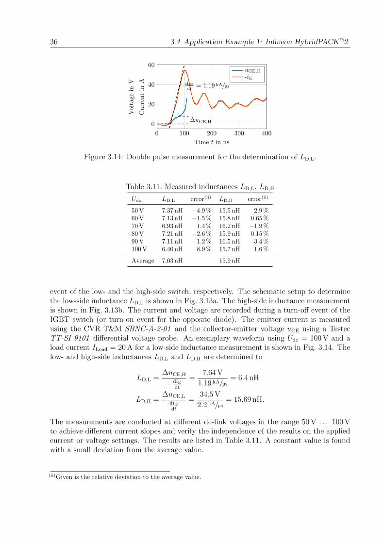
36 3.4 Application Example 1: Infineon HybridPACK™2
0 100 200 300 400
0
20
40
60
Time t in ns
Voltagein
V
Currentin
A
uCE,H
-iE
∆uCE,H
-diEdt = 1.19 kA/µs
Figure 3.14: Double pulse measurement for the determination of LD,L.
Table 3.11: Measured inductances LD,L, LD,H
Udc LD,L error(ii) LD,H error(ii)
50 V 7.37 nH −4.9 % 15.5 nH 2.9 %60 V 7.13 nH −1.5 % 15.8 nH 0.65 %70 V 6.93 nH 1.4 % 16.2 nH −1.9 %80 V 7.21 nH −2.6 % 15.9 nH 0.15 %90 V 7.11 nH −1.2 % 16.5 nH −3.4 %100 V 6.40 nH 8.9 % 15.7 nH 1.6 %
Average 7.03 nH 15.9 nH
event of the low- and the high-side switch, respectively. The schematic setup to determinethe low-side inductance LD,L is shown in Fig. 3.13a. The high-side inductance measurementis shown in Fig. 3.13b. The current and voltage are recorded during a turn-off event of theIGBT switch (or turn-on event for the opposite diode). The emitter current is measuredusing the CVR T&M SBNC-A-2-01 and the collector-emitter voltage uCE using a TestecTT-SI 9101 differential voltage probe. An exemplary waveform using Udc = 100 V and aload current ILoad = 20 A for a low-side inductance measurement is shown in Fig. 3.14. Thelow- and high-side inductances LD,L and LD,H are determined to
LD,L =∆uCE,H
−diEdt
=7.64 V
1.19 kA/µs= 6.4 nH
LD,H =∆uCE,L
diCdt
=34.5 V
2.2 kA/µs= 15.69 nH.
The measurements are conducted at different dc-link voltages in the range 50 V . . . 100 Vto achieve different current slopes and verify the independence of the results on the appliedcurrent or voltage settings. The results are listed in Table 3.11. A constant value is foundwith a small deviation from the average value.
(ii)Given is the relative deviation to the average value.
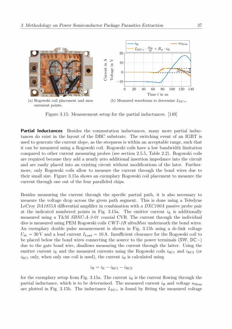
3 Methodology on Power Semiconductor Package Parasitics Extraction 37
111111111111111111111 222222222222222222222
333333333333333333333
444444444444444444444
555555555555555555555
666666666666666666666
777777777777777777777 101010101010101010101010101010101010101010
111111111111111111111111111111111111111111
121212121212121212121212121212121212121212
131313131313131313131313131313131313131313
151515151515151515151515151515151515151515
161616161616161616161616161616161616161616171717171717171717171717171717171717171717191919191919191919191919191919191919191919
181818181818181818181818181818181818181818
202020202020202020202020202020202020202020212121212121212121212121212121212121212121
232323232323232323232323232323232323232323222222222222222222222222222222222222222222
(a) Rogowski coil placement and mea-surement points.
0 20 40 60 80 100 120 140
−10
0
10
20
Time t in ns
Currentin
A
Voltage
inV
iH uMeas
LDC+ · diHdt +Rσ · iH
∆uMeas
(b) Measured waveforms to determine LDC+.
Figure 3.15: Measurement setup for the partial inductances. [149]
Partial Inductances Besides the commutation inductances, many more partial induc-tances do exist in the layout of the DBC substrate. The switching event of an IGBT isused to generate the current slope, as the steepness is within an acceptable range, such thatit can be measured using a Rogowski coil. Rogowski coils have a low bandwidth limitationcompared to other current measuring probes (see section 2.5.5, Table 2.2). Rogowski coilsare required because they add a nearly zero additional insertion impedance into the circuitand are easily placed into an existing circuit without modifications of the later. Further-more, only Rogowski coils allow to measure the current through the bond wires due totheir small size. Figure 3.15a shows an exemplary Rogowski coil placement to measure thecurrent through one out of the four paralleled chips.
Besides measuring the current through the specific partial path, it is also necessary tomeasure the voltage drop across the given path segment. This is done using a TeledyneLeCroy DA1855A differential amplifier in combination with a DXC100A passive probe pairat the indicated numbered points in Fig. 3.15a. The emitter current iE is additionallymeasured using a T&M SBNC-A-2-01 coaxial CVR. The current through the individualdies is measured using PEM Rogowski coils CWT-1B ultraMini underneath the bond wires.An exemplary double pulse measurement is shown in Fig. 3.15b using a dc-link voltageUdc = 30 V and a load current ILoad = 10 A. Insufficient clearance for the Rogowski coil tobe placed below the bond wires connecting the source to the power terminals (SW, DC−)due to the gate bond wire, disallows measuring the current through the latter. Using theemitter current iE and the measured currents using the Rogowski coils iRC1 and iRC2 (oriRC1 only, when only one coil is used), the current iH is calculated using
iH = iE − iRC1 − iRC2
for the exemplary setup from Fig. 3.15a. The current iH is the current flowing through thepartial inductance, which is to be determined. The measured current iH and voltage uMeas
are plotted in Fig. 3.15b. The inductance LDC+ is found by fitting the measured voltage
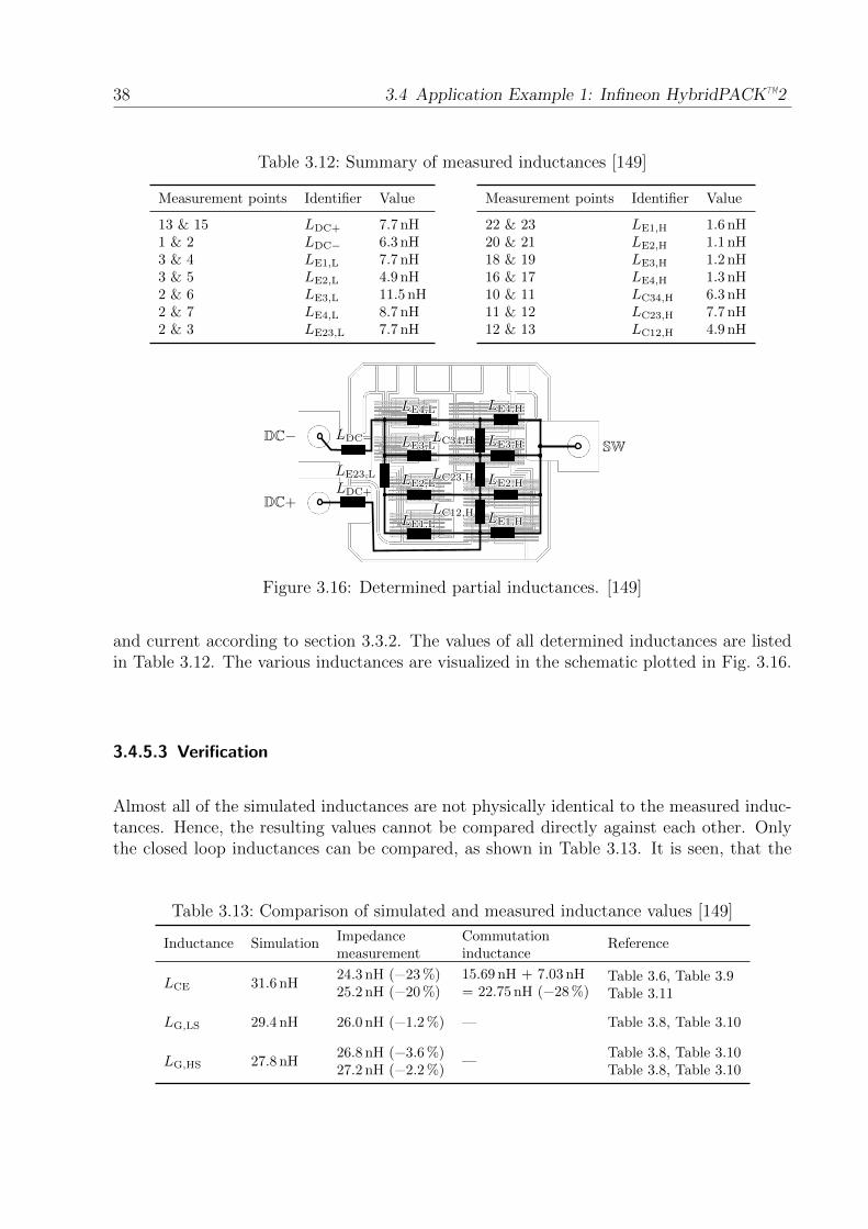
38 3.4 Application Example 1: Infineon HybridPACK™2
Table 3.12: Summary of measured inductances [149]
Measurement points Identifier Value
13 & 15 LDC+ 7.7 nH1 & 2 LDC− 6.3 nH3 & 4 LE1,L 7.7 nH3 & 5 LE2,L 4.9 nH2 & 6 LE3,L 11.5 nH2 & 7 LE4,L 8.7 nH2 & 3 LE23,L 7.7 nH
Measurement points Identifier Value
22 & 23 LE1,H 1.6 nH20 & 21 LE2,H 1.1 nH18 & 19 LE3,H 1.2 nH16 & 17 LE4,H 1.3 nH10 & 11 LC34,H 6.3 nH11 & 12 LC23,H 7.7 nH12 & 13 LC12,H 4.9 nH
LDC+LDC+LDC+LDC+LDC+LDC+LDC+LDC+LDC+LDC+LDC+LDC+LDC+LDC+LDC+LDC+LDC+LDC+LDC+LDC+LDC+
LDC−LDC−LDC−LDC−LDC−LDC−LDC−LDC−LDC−LDC−LDC−LDC−LDC−LDC−LDC−LDC−LDC−LDC−LDC−LDC−LDC−
LE23,LLE23,LLE23,LLE23,LLE23,LLE23,LLE23,LLE23,LLE23,LLE23,LLE23,LLE23,LLE23,LLE23,LLE23,LLE23,LLE23,LLE23,LLE23,LLE23,LLE23,L
LE1,LLE1,LLE1,LLE1,LLE1,LLE1,LLE1,LLE1,LLE1,LLE1,LLE1,LLE1,LLE1,LLE1,LLE1,LLE1,LLE1,LLE1,LLE1,LLE1,LLE1,L
LE2,LLE2,LLE2,LLE2,LLE2,LLE2,LLE2,LLE2,LLE2,LLE2,LLE2,LLE2,LLE2,LLE2,LLE2,LLE2,LLE2,LLE2,LLE2,LLE2,LLE2,L
LE3,LLE3,LLE3,LLE3,LLE3,LLE3,LLE3,LLE3,LLE3,LLE3,LLE3,LLE3,LLE3,LLE3,LLE3,LLE3,LLE3,LLE3,LLE3,LLE3,LLE3,L
LE4,LLE4,LLE4,LLE4,LLE4,LLE4,LLE4,LLE4,LLE4,LLE4,LLE4,LLE4,LLE4,LLE4,LLE4,LLE4,LLE4,LLE4,LLE4,LLE4,LLE4,L
LC23,HLC23,HLC23,HLC23,HLC23,HLC23,HLC23,HLC23,HLC23,HLC23,HLC23,HLC23,HLC23,HLC23,HLC23,HLC23,HLC23,HLC23,HLC23,HLC23,HLC23,H
LC12,HLC12,HLC12,HLC12,HLC12,HLC12,HLC12,HLC12,HLC12,HLC12,HLC12,HLC12,HLC12,HLC12,HLC12,HLC12,HLC12,HLC12,HLC12,HLC12,HLC12,H
LC34,HLC34,HLC34,HLC34,HLC34,HLC34,HLC34,HLC34,HLC34,HLC34,HLC34,HLC34,HLC34,HLC34,HLC34,HLC34,HLC34,HLC34,HLC34,HLC34,HLC34,H
LE1,HLE1,HLE1,HLE1,HLE1,HLE1,HLE1,HLE1,HLE1,HLE1,HLE1,HLE1,HLE1,HLE1,HLE1,HLE1,HLE1,HLE1,HLE1,HLE1,HLE1,H
LE2,HLE2,HLE2,HLE2,HLE2,HLE2,HLE2,HLE2,HLE2,HLE2,HLE2,HLE2,HLE2,HLE2,HLE2,HLE2,HLE2,HLE2,HLE2,HLE2,HLE2,H
LE3,HLE3,HLE3,HLE3,HLE3,HLE3,HLE3,HLE3,HLE3,HLE3,HLE3,HLE3,HLE3,HLE3,HLE3,HLE3,HLE3,HLE3,HLE3,HLE3,HLE3,H
LE4,HLE4,HLE4,HLE4,HLE4,HLE4,HLE4,HLE4,HLE4,HLE4,HLE4,HLE4,HLE4,HLE4,HLE4,HLE4,HLE4,HLE4,HLE4,HLE4,HLE4,H
DC−
DC+
SW
Figure 3.16: Determined partial inductances. [149]
and current according to section 3.3.2. The values of all determined inductances are listedin Table 3.12. The various inductances are visualized in the schematic plotted in Fig. 3.16.
3.4.5.3 Verification
Almost all of the simulated inductances are not physically identical to the measured induc-tances. Hence, the resulting values cannot be compared directly against each other. Onlythe closed loop inductances can be compared, as shown in Table 3.13. It is seen, that the
Table 3.13: Comparison of simulated and measured inductance values [149]
Inductance SimulationImpedancemeasurement
Commutationinductance
Reference
LCE 31.6 nH24.3 nH (−23 %) 15.69 nH + 7.03 nH
= 22.75 nH (−28 %)Table 3.6, Table 3.9Table 3.1125.2 nH (−20 %)
LG,LS 29.4 nH 26.0 nH (−1.2 %) — Table 3.8, Table 3.10
LG,HS 27.8 nH26.8 nH (−3.6 %)
—Table 3.8, Table 3.10
27.2 nH (−2.2 %) Table 3.8, Table 3.10

3 Methodology on Power Semiconductor Package Parasitics Extraction 39
gate inductance values match well between the simulation and measurements (less than 5 %deviation). However, a larger deviation is seen for the power loop inductance LCE. Twopossible causes for the observed deviation are identified. First, the intrinsic capacitances ofthe power semiconductors add additional resonances and make the impedance extractionmore difficult. Second, the observed current contraction in the simulation (see Fig. 3.9) doesnot properly reflect reality due to the missing IGBTs in the simulation model. To verify thepartial inductance values, a switching model is developed in section 3.6, which comparesthe resulting simulated switching transients to the measured switching waveforms.
3.5 Application Example 2: MOSFET in a TO-247Package
A second, commonly employed package in power electronic converters is the TO-247 packageas seen in Fig. 3.17. It is used for many discrete power semiconductors, but also for passivecomponents (e.g., power resistors). Investigations regarding the parasitic inductances ofthe TO-247 package are presented in this section using the SiC MOSFET C2M0040120D.A photograph of the opened package showing the bare die is seen in Fig. 3.17a. The 3DCAD model, which is used in the FE simulations, is shown in Fig. 3.17b. The investigationfocuses only on the inductive components, as the relevant capacitance is the tab-to-heat sinkcapacitance. However, this capacitance is mostly influenced by the external TIM, whichensures an electrical insulation from the tab to the heat sink A large variety of differentTIMs is available and their choice depends on the design of the power electronic system andnot on the TO-247 package.
G D S
(a) Photograph of an opened TO-247 package. [37] (b) 3D CAD model of the package.
Figure 3.17: SiC MOSFET in a TO-247 pacakage.
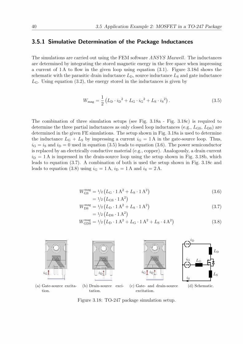
40 3.5 Application Example 2: MOSFET in a TO-247 Package
3.5.1 Simulative Determination of the Package Inductances
The simulations are carried out using the FEM software ANSYS Maxwell . The inductancesare determined by integrating the stored magnetic energy in the free space when impressinga current of 1 A to flow in the given loop using equation (3.1). Figure 3.18d shows theschematic with the parasitic drain inductance LD, source inductance LS and gate inductanceLG. Using equation (3.2), the energy stored in the inductances is given by
Wmag =1
2
(LD · iD2 + LG · iG2 + LS · iS2
). (3.5)
The combination of three simulation setups (see Fig. 3.18a - Fig. 3.18c) is required todetermine the three partial inductances as only closed loop inductances (e.g., LGS, LDS) aredetermined in the given FE simulations. The setup shown in Fig. 3.18a is used to determinethe inductance LG + LS by impressing a current iG = 1 A in the gate-source loop. Thus,iG = iS and iD = 0 used in equation (3.5) leads to equation (3.6). The power semiconductoris replaced by an electrically conductive material (e.g., copper). Analogously, a drain currentiD = 1 A is impressed in the drain-source loop using the setup shown in Fig. 3.18b, whichleads to equation (3.7). A combination of both is used the setup shown in Fig. 3.18c andleads to equation (3.8) using iG = 1 A, iD = 1 A and iS = 2 A.
WmagGS = 1/2
(LG · 1 A2 + LS · 1 A2
)(3.6)
= 1/2(LGS · 1 A2
)Wmag
DS = 1/2(LD · 1 A2 + LS · 1 A2
)(3.7)
= 1/2(LDS · 1 A2
)Wmag
GDS = 1/2(LD · 1 A2 + LG · 1 A2 + LS · 4 A2
)(3.8)
iG
(a) Gate-source excita-tion.
iD
(b) Drain-source exci-tation.
iG iD
(c) Gate- and drain-sourceexcitation.
LD
LS
LG
iD
iG
iS
(d) Schematic.
Figure 3.18: TO-247 package simulation setup.
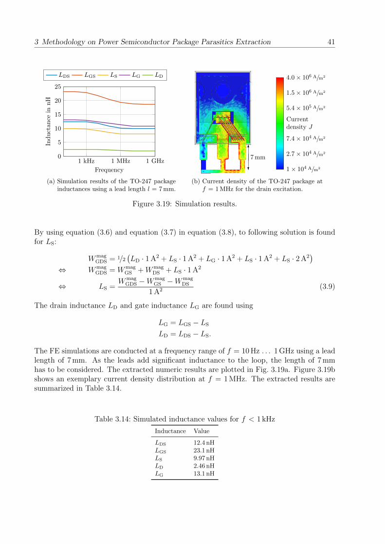
3 Methodology on Power Semiconductor Package Parasitics Extraction 41
LDS LGS LS LG LD
1 kHz 1 MHz 1 GHz0
5
10
15
20
25
Frequency
Inductan
cein
nH
(a) Simulation results of the TO-247 packageinductances using a lead length l = 7 mm.
7 mm6
? 1× 10⁴ A/m2
2.7× 10⁴ A/m2
7.4× 10⁴ A/m2
Currentdensity J
5.4× 10⁵ A/m2
1.5× 10⁶ A/m2
4.0× 10⁶ A/m2
(b) Current density of the TO-247 package atf = 1 MHz for the drain excitation.
Figure 3.19: Simulation results.
By using equation (3.6) and equation (3.7) in equation (3.8), to following solution is foundfor LS:
WmagGDS = 1/2
(LD · 1 A2 + LS · 1 A2 + LG · 1 A2 + LS · 1 A2 + LS · 2 A2
)⇔ Wmag
GDS = WmagGS +Wmag
DS + LS · 1 A2
⇔ LS =Wmag
GDS −WmagGS −Wmag
DS
1 A2 (3.9)
The drain inductance LD and gate inductance LG are found using
LG = LGS − LS
LD = LDS − LS.
The FE simulations are conducted at a frequency range of f = 10 Hz . . . 1 GHz using a leadlength of 7 mm. As the leads add significant inductance to the loop, the length of 7 mmhas to be considered. The extracted numeric results are plotted in Fig. 3.19a. Figure 3.19bshows an exemplary current density distribution at f = 1 MHz. The extracted results aresummarized in Table 3.14.
Table 3.14: Simulated inductance values for f < 1 kHz
Inductance Value
LDS 12.4 nHLGS 23.1 nHLS 9.97 nHLD 2.46 nHLG 13.1 nH

42 3.5 Application Example 2: MOSFET in a TO-247 Package
3.5.2 Experimental Determination of Parasitic Inductances
The experimental determination of the previously simulated inductances is shown in thissection using the methodology described in section 3.3.2. The current pulse generator (seesection 2.5.1) is used to generate the required current pulses. A schematic of the setup isshown in Fig. 3.20a. The DUT SDUT is turned on using a gate voltage Ucc = 15 V and highimpedance gate resistance RG = 100 Ω. The high impedance gate resistance disallows aquick change of charge in the gate capacitance CGS and therewith allows the measurementof the virtual source potential (Sv) directly at the chip, hence across the inductance LS.A sudden increase of the drain-source current iS shifts the virtual source potential Sv ofthe chip due to the inductive voltage drop across LS. The high impedance gate resistanceprevents a current flow in the gate path and therefore allows to monitor the virtual sourcevoltage Sv. Analogously, the voltage across LD equals uGD using the virtual drain potential,which equals the virtual source potential Sv. A photograph of the setup is pictured inFig. 3.20b, showing the placement of the current and voltage probes. The measurementwaveforms are plotted in Fig. 3.21 for the three different cases.
The resulting values for the different parasitic inductances are listed in Table 3.15 including acomparison to the simulated values. Except for the drain inductance LD, a relative deviationof less than 10 % is found between the simulated and measured values. However, as theabsolute value of the drain inductance LD is small comparing to the remaining inductances,the deviation error of LD + LS compared to the simulation or the LDS measurement isvery small. It is noticed, that this methodology does not allow the determination of the
Udc
R
L1S1
S2D
Current Pulse Generator DUT
LD
LS
LG
iS
uDS
SDUT
RG
uGS Ucc
Lσ/2
Lσ/2
C
CGD
CGSSv
uGD
D
S
G
(a) Schematic of the setup.
Current Pulse Generator
Lσ
DUT
iS
uDS
7mm
(b) Photograph of the setupincluding the measurementprobes.
Figure 3.20: Partial inductance extraction test setup of the TO-247 package.
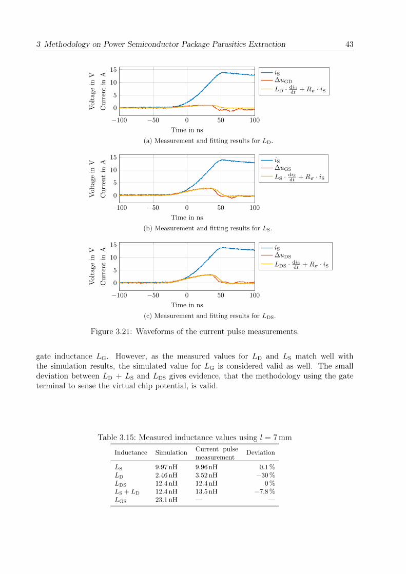
3 Methodology on Power Semiconductor Package Parasitics Extraction 43
−100 −50 0 50 100
0
5
10
15
Time in ns
Vol
tage
inV
Cu
rren
tin
A iS∆uGD
LD · diSdt + Rσ · iS
(a) Measurement and fitting results for LD.
−100 −50 0 50 100
0
5
10
15
Time in ns
Volt
age
inV
Cu
rren
tin
A iS∆uGS
LS · diSdt + Rσ · iS
(b) Measurement and fitting results for LS.
−100 −50 0 50 100
0
5
10
15
Time in ns
Vol
tage
inV
Cu
rren
tin
A iS∆uDS
LDS · diSdt + Rσ · iS
(c) Measurement and fitting results for LDS.
Figure 3.21: Waveforms of the current pulse measurements.
gate inductance LG. However, as the measured values for LD and LS match well withthe simulation results, the simulated value for LG is considered valid as well. The smalldeviation between LD + LS and LDS gives evidence, that the methodology using the gateterminal to sense the virtual chip potential, is valid.
Table 3.15: Measured inductance values using l = 7 mm
Inductance SimulationCurrent pulsemeasurement
Deviation
LS 9.97 nH 9.96 nH 0.1 %LD 2.46 nH 3.52 nH −30 %LDS 12.4 nH 12.4 nH 0 %LS + LD 12.4 nH 13.5 nH −7.8 %LGS 23.1 nH — —
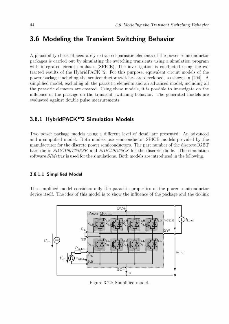
44 3.6 Modeling the Transient Switching Behavior
3.6 Modeling the Transient Switching Behavior
A plausibility check of accurately extracted parasitic elements of the power semiconductorpackages is carried out by simulating the switching transients using a simulation programwith integrated circuit emphasis (SPICE). The investigation is conducted using the ex-tracted results of the HybridPACK™2. For this purpose, equivalent circuit models of thepower package including the semiconductor switches are developed, as shown in [204]. Asimplified model, excluding all the parasitic elements and an advanced model, including allthe parasitic elements are created. Using these models, it is possible to investigate on theinfluence of the package on the transient switching behavior. The generated models areevaluated against double pulse measurements.
3.6.1 HybridPACK™2 Simulation Models
Two power package models using a different level of detail are presented: An advancedand a simplified model. Both models use semiconductor SPICE models provided by themanufacturer for the discrete power semiconductors. The part number of the discrete IGBTbare die is SIGC100T65R3E and SIDC50D65C8 for the discrete diode. The simulationsoftware SIMetrix is used for the simulations. Both models are introduced in the following.
3.6.1.1 Simplified Model
The simplified model considers only the parasitic properties of the power semiconductordevice itself. The idea of this model is to show the influence of the package and the dc-link
SW
DC−
Udc
uGE,LUcc
DC+
RG,LS
Power Module
S4,L S3,L S2,L S1,LD4,L D3,L D2,L D1,L
S4,H S3,H S2,H S1,H
uCE,L
iE
ILoadD4,H D3,H D2,H D1,H
GL
KE
GL
KE
uCE,H
Figure 3.22: Simplified model.
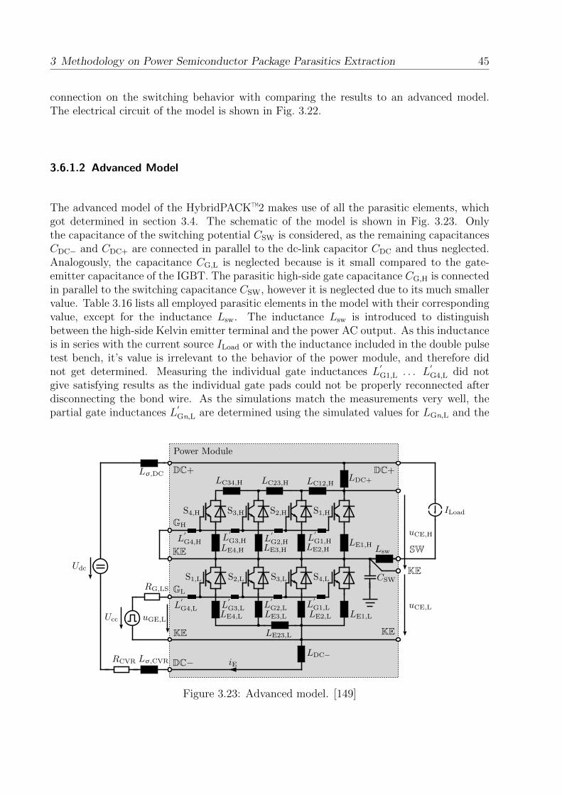
3 Methodology on Power Semiconductor Package Parasitics Extraction 45
connection on the switching behavior with comparing the results to an advanced model.The electrical circuit of the model is shown in Fig. 3.22.
3.6.1.2 Advanced Model
The advanced model of the HybridPACK™2 makes use of all the parasitic elements, whichgot determined in section 3.4. The schematic of the model is shown in Fig. 3.23. Onlythe capacitance of the switching potential CSW is considered, as the remaining capacitancesCDC− and CDC+ are connected in parallel to the dc-link capacitor CDC and thus neglected.Analogously, the capacitance CG,L is neglected because is it small compared to the gate-emitter capacitance of the IGBT. The parasitic high-side gate capacitance CG,H is connectedin parallel to the switching capacitance CSW, however it is neglected due to its much smallervalue. Table 3.16 lists all employed parasitic elements in the model with their correspondingvalue, except for the inductance Lsw. The inductance Lsw is introduced to distinguishbetween the high-side Kelvin emitter terminal and the power AC output. As this inductanceis in series with the current source ILoad or with the inductance included in the double pulsetest bench, it’s value is irrelevant to the behavior of the power module, and therefore didnot get determined. Measuring the individual gate inductances L
′G1,L . . . L
′G4,L did not
give satisfying results as the individual gate pads could not be properly reconnected afterdisconnecting the bond wire. As the simulations match the measurements very well, thepartial gate inductances L
′Gn,L are determined using the simulated values for LGn,L and the
ILoad
DC+
DC−
KE
GL
uGE,L
SW
S1,HS2,HS3,HS4,H
Lσ,DC
LDC−
LDC+LC12,HLC23,HLC34,H
LE4,H LE3,H LE2,HLE1,H
LE4,L LE3,L LE2,L LE1,L
LE23,L
L′G4,H
L′G3,H L
′G2,H
L′G1,H
Udc
L′G4,L L
′G3,L L
′G2,L L
′G1,L
S1,L S2,L S3,L S4,L
DC+
CSW
Lσ,CVR
RG,LS
Ucc
GH
KE
Power Module
RCVR
Lsw
iE
KE
KE
uCE,L
uCE,H
Figure 3.23: Advanced model. [149]
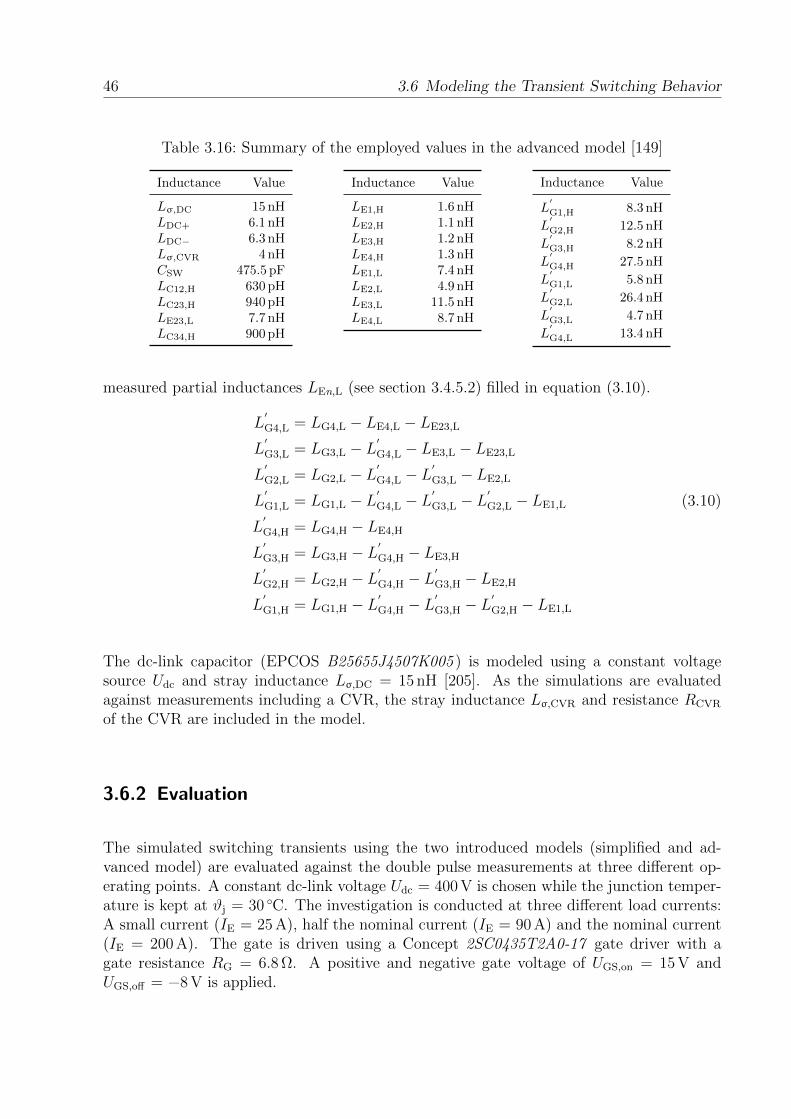
46 3.6 Modeling the Transient Switching Behavior
Table 3.16: Summary of the employed values in the advanced model [149]
Inductance Value
Lσ,DC 15 nHLDC+ 6.1 nHLDC− 6.3 nHLσ,CVR 4 nHCSW 475.5 pFLC12,H 630 pHLC23,H 940 pHLE23,L 7.7 nHLC34,H 900 pH
Inductance Value
LE1,H 1.6 nHLE2,H 1.1 nHLE3,H 1.2 nHLE4,H 1.3 nHLE1,L 7.4 nHLE2,L 4.9 nHLE3,L 11.5 nHLE4,L 8.7 nH
Inductance Value
L′G1,H 8.3 nH
L′G2,H 12.5 nH
L′G3,H 8.2 nH
L′G4,H 27.5 nH
L′G1,L 5.8 nH
L′G2,L 26.4 nH
L′G3,L 4.7 nH
L′G4,L 13.4 nH
measured partial inductances LEn,L (see section 3.4.5.2) filled in equation (3.10).
L′
G4,L = LG4,L − LE4,L − LE23,L
L′
G3,L = LG3,L − L′
G4,L − LE3,L − LE23,L
L′
G2,L = LG2,L − L′
G4,L − L′
G3,L − LE2,L
L′
G1,L = LG1,L − L′
G4,L − L′
G3,L − L′
G2,L − LE1,L (3.10)
L′
G4,H = LG4,H − LE4,H
L′
G3,H = LG3,H − L′
G4,H − LE3,H
L′
G2,H = LG2,H − L′
G4,H − L′
G3,H − LE2,H
L′
G1,H = LG1,H − L′
G4,H − L′
G3,H − L′
G2,H − LE1,L
The dc-link capacitor (EPCOS B25655J4507K005 ) is modeled using a constant voltagesource Udc and stray inductance Lσ,DC = 15 nH [205]. As the simulations are evaluatedagainst measurements including a CVR, the stray inductance Lσ,CVR and resistance RCVR
of the CVR are included in the model.
3.6.2 Evaluation
The simulated switching transients using the two introduced models (simplified and ad-vanced model) are evaluated against the double pulse measurements at three different op-erating points. A constant dc-link voltage Udc = 400 V is chosen while the junction temper-ature is kept at ϑj = 30 C. The investigation is conducted at three different load currents:A small current (IE = 25 A), half the nominal current (IE = 90 A) and the nominal current(IE = 200 A). The gate is driven using a Concept 2SC0435T2A0-17 gate driver with agate resistance RG = 6.8 Ω. A positive and negative gate voltage of UGS,on = 15 V andUGS,off = −8 V is applied.
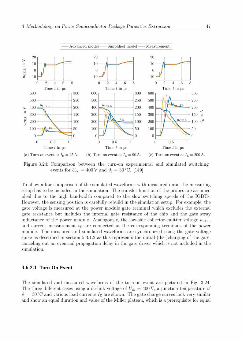
3 Methodology on Power Semiconductor Package Parasitics Extraction 47
Advanced model Simplified model Measurement
0 2 4 6 8
−10
0
10
20
Time t in µs
uGE,L
inV
0 0.5 1
0
100
200
300
400
500
600
Time t in µs
uCE,L
inV
0
50
100
150
200
250
300
uCE,L
iE
(a) Turn-on event at IE = 25 A.
0 2 4 6 8
−10
0
10
20
Time t in µs
0 0.5 1
0
100
200
300
400
500
600
Time t in µs
0
50
100
150
200
250
300
uCE,L
iE
(b) Turn-on event at IE = 90 A.
0 2 4 6 8
−10
0
10
20
Time t in µs
0 0.5 1
0
100
200
300
400
500
600
Time t in µs
0
50
100
150
200
250
300
i Ein
A
uCE,L
iE
(c) Turn-on event at IE = 200 A.
Figure 3.24: Comparison between the turn-on experimental and simulated switchingevents for Udc = 400 V and ϑj = 30 C. [149]
To allow a fair comparison of the simulated waveforms with measured data, the measuringsetup has to be included in the simulation. The transfer function of the probes are assumedideal due to the high bandwidth compared to the slow switching speeds of the IGBTs.However, the sensing position is carefully rebuild in the simulation setup. For example, thegate voltage is measured at the power module gate terminal which excludes the externalgate resistance but includes the internal gate resistance of the chip and the gate strayinductance of the power module. Analogously, the low-side collector-emitter voltage uCE,L
and current measurement iE are connected at the corresponding terminals of the powermodule. The measured and simulated waveforms are synchronized using the gate voltagespike as described in section 5.3.1.2 as this represents the initial (dis-)charging of the gate,canceling out an eventual propagation delay in the gate driver which is not included in thesimulation.
3.6.2.1 Turn-On Event
The simulated and measured waveforms of the turn-on event are pictured in Fig. 3.24.The three different cases using a dc-link voltage of Udc = 400 V, a junction temperature ofϑj = 30 C and various load currents IE are shown. The gate charge curves look very similarand show an equal duration and value of the Miller plateau, which is a prerequisite for equal
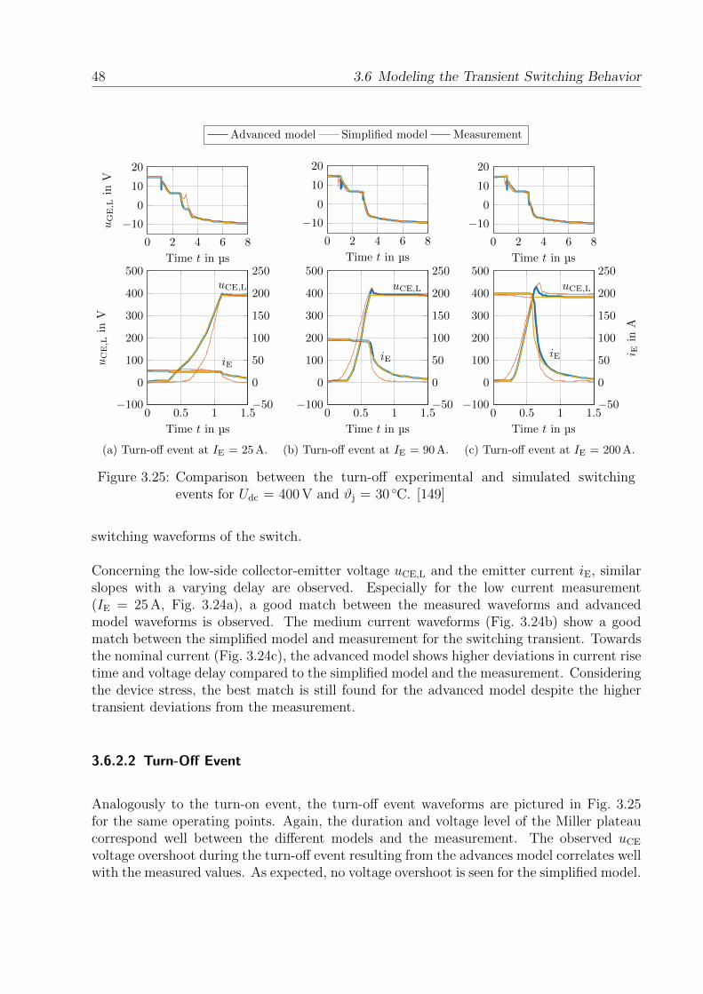
48 3.6 Modeling the Transient Switching Behavior
Advanced model Simplified model Measurement
0 2 4 6 8
−10
0
10
20
Time t in µs
uGE,L
inV
0 0.5 1 1.5−100
0
100
200
300
400
500
Time t in µs
uCE,L
inV
−50
0
50
100
150
200
250uCE,L
iE
(a) Turn-off event at IE = 25 A.
0 2 4 6 8
−10
0
10
20
Time t in µs
0 0.5 1 1.5−100
0
100
200
300
400
500
Time t in µs
−50
0
50
100
150
200
250
uCE,L
iE
(b) Turn-off event at IE = 90 A.
0 2 4 6 8
−10
0
10
20
Time t in µs
0 0.5 1 1.5−100
0
100
200
300
400
500
Time t in µs
−50
0
50
100
150
200
250
i Ein
A
uCE,L
iE
(c) Turn-off event at IE = 200 A.
Figure 3.25: Comparison between the turn-off experimental and simulated switchingevents for Udc = 400 V and ϑj = 30 C. [149]
switching waveforms of the switch.
Concerning the low-side collector-emitter voltage uCE,L and the emitter current iE, similarslopes with a varying delay are observed. Especially for the low current measurement(IE = 25 A, Fig. 3.24a), a good match between the measured waveforms and advancedmodel waveforms is observed. The medium current waveforms (Fig. 3.24b) show a goodmatch between the simplified model and measurement for the switching transient. Towardsthe nominal current (Fig. 3.24c), the advanced model shows higher deviations in current risetime and voltage delay compared to the simplified model and the measurement. Consideringthe device stress, the best match is still found for the advanced model despite the highertransient deviations from the measurement.
3.6.2.2 Turn-Off Event
Analogously to the turn-on event, the turn-off event waveforms are pictured in Fig. 3.25for the same operating points. Again, the duration and voltage level of the Miller plateaucorrespond well between the different models and the measurement. The observed uCE
voltage overshoot during the turn-off event resulting from the advances model correlates wellwith the measured values. As expected, no voltage overshoot is seen for the simplified model.
3 Methodology on Power Semiconductor Package Parasitics Extraction 49
However, the simplified and the advanced model result in very similar collector-emittervoltage and emitter current waveforms, but show some deviation from the measured curves.This leads to two possible conclusions: Either the package does not have a major impacton the switching transients, which is disregarded and further discussed in chapter 4, or thesemiconductor models represent behavioral models of the switches and not pure physicalsemiconductor models. Further investigations on the provided semiconductor models haveto be conducted.
3.7 Summary
In this chapter, various methodology to extract the electrical parasitic elements from powerpackages have been investigated. The parasitic elements of interest are the capacitance andinductance values due to the packaging, disregarding the intrinsic power semiconductor par-asitics. Both parasitic types have first been investigated using FE simulations and verifiedby various experimental approaches. To cover a wide range of packaging types, the method-ologies have been applied to a HybridPACK™2 to represent large power packages and on aTO-247 package, which represents a very common package for discrete power devices. Theexperimental determination of capacitance values is conducted using impedance measure-ments. A very good correlation between the measured and calculated results is found forboth packaging types. Concerning the extraction of parasitic inductance, three differentexperimental methodologies are employed: impedance measurements, impressing currentpulses and using switching events. The different approaches allow the extraction of vari-ous inductive quantities from the power package. The presented methodology shows thatmost parasitic parameters of a power semiconductor are found using various measurementtechniques.
Besides comparing the simulated parasitic element values to the experimental results, a ver-ification based on the time-domain simulation of switching transients have been conductedusing the HybridPACK™2 power device. An evaluation of the measured transient waveformswith the simulated models showed good agreement, however some deviations are seen in thedetailed view. As the deviations between the measurements and modeled transients of theHybridPACK™2, are within the same range, it is concluded, that the switching behaviormainly relies on the power semiconductor rather than on the packaging. However, the volt-age overshoot during the turn-off event in the advanced model is in good correlation withthe measured values. The source for the observed deviations could not be clearly identifiedas too many unknown factors have a large influence on the switching behavior. However,the author believes, that the power semiconductor models, which are provided by the man-ufacturer, are behavioral models and not pure physical models. A detailed investigation onthe semiconductor models is required to identify their accuracy.
However, for fast switching power semiconductors, it is expected that the parasitic elementshave a much higher influence on the switching behavior rather than the power semiconductor

50 3.7 Summary
itself (see e.g., [164]). Therefore, the influence of the stray inductances on the switchingbehavior of SiC power MOSFETs is investigated in more detail in chapter 4.
4 Influence of Parasitic Inductances on theSwitching Behavior
Besides determining the parasitic inductances of a given DBC structure or switching cellin general, the influence of the parasitic inductance on the switching transients and onthe stress of the power semiconductors is investigated. In this chapter, a SiC MOSFETswitching cell on a PCB with variable inductances is used to conduct these investigations.The measurements are conducted in the double pulse test bench (see section 2.5.3) with theprobe setup as introduced in section 2.5.5.
Especially the high-side diode voltage is of interest as this is most of the times not regarded inliterature. Non negligible voltage overshoots are observed, which are responsible for failuresespecially at fast switching operations. Furthermore, the investigated switching speed inliterature varies massively from very slow (comparable to the switching speed of IGBTs)[141] to very fast [125] and only discrete operating points, which does not allow to drawgeneral conclusions. A detailed analysis with a massive parameter variation using a singlesetup is not found in literature.
Besides the influence of the power loop inductance, the gate and common-source inductancesare part of the investigation. Both low- and high-side inductance values are varied, whileonly the low-side MOSFET is switched. The found results are applied analogously forhigh-side switching.
4.1 Hardware Setup
A single setup is used for all the investigations to allow a good comparability. Differentsetups would include further (unwanted) influence on the switching behavior besides theinfluence of the stray inductances. However, a compromise is made at this point, as a singleboard containing several variable inductances does not represent an optimized switchingcell. The schematic of the switching cell with the indicated variable stray inductances isshown in Fig. 4.1. The switching cell employs 1200 V SiC MOSFETs (S1 and S2) (CreeCMP2-1200-0025B) with a current rating of 98 A [206] each. The dc-link capacitor CDC
mounted on the PCB is a CeraLink™ ceramic capacitor [207]. The MOSFET source currentiS is measured using a T&M Research SDN-015 CVR. In total, five variable inductancesare installed: the power loop inductance LLoop, the low- and high-side common-source in-
51

52 4.1 Hardware Setup
Ucc
uGS
CDC
RG,HS
RG,LS
LG,HS
LG,LS
LCS,HS
LCS,LS
∆LLoop
S1
S2
Lσ/2
Lσ/2
DC+
DC−
SW
Lσ,CVR
RCVR
uGS,HS
Ucc
iS
Figure 4.1: Schematic of the switching cell with variable inductances.
LG,HS DC+
DC−SW
CDC
CVR
∆LLoop
LG,LS
Low-side gate driver
High-side gate driver
Gate resistance RG,HS
Low-side MOSFET S2
High-side MOSFET S1
LCS,LS
LCS,HS
Figure 4.2: Photograph of the PCB with variable inductances. [51]
ductances LCS,LS and LCS,HS and the low- and high-side gate inductances LG,LS and LG,HS.The manufactured PCB is pictured in Fig. 4.2. The board is designed to connect directly tothe double pulse test bench. The employed probes for the various measurement quantitiesare listed in Table 4.1.
Table 4.1: Measurement equipment
Manufacturer Part Nr. Symbol Delay Bandwidth
PMK BumbleBee® uDS, uDiode 12.3 ns 300 MHzTestec TT-SI 9110 uGS 11.7 ns 100 MHzT&M Research SDN-015 iS 5.4 ns (i) 1200 MHz
(i)In combination with 1 m coaxial cable.

4 Influence of Parasitic Inductances on the Switching Behavior 53
(a) Pin header as variable inductance ad-justment.
0 5 10 15 20 2525
30
35
40
45
Jumper position
Lloop
inn
H
MeasurementLinear fit
(b) Measured power loop inductanceLLoop depending on jumper position.
Figure 4.3: Variable inductance setup.
4.1.1 Variable Gate and Power Loop Inductance
To build an adjustable inductance, which gives reliable and repeatable results, a pin header,as shown in Fig. 4.3a, is used. All the pins from one side of the pin header are connectedtogether and the jumper closes the loop at a given position. The jumper position defines thelength of the loop and hence, the inductance value. The resulting inductance is measuredusing the current pulse methodology (see section 2.5.1 and section 3.3.2) including the strayinductance of the dc-link connection (Lσ) and the CVR inductance (Lσ,CVR). The resultinginductance is plotted in dependency of the jumper position in Fig. 4.3b. An average stepsize of 800 pH and 1.1 nH per pin position is achieved for the power loop inductance andthe gate loop inductance, respectively. Due to the numerous variable inductances and theincluded CVR, the dimensions of the switching cell cannot be further reduced, hence aminimum total loop inductance LLoop = ∆LLoop + Lσ + LCS,HS + LCS,LS + Lσ,CVR = 25 nHcannot be undergone. The stray inductance of the CVR is Lσ,CVR = 7 nH.
4.1.2 Variable Common-Source Inductance
In contrast to the variation of the gate and power loop inductances, the common-sourceinductance is not varied via a pin header. A close-up view of the PCB is shown in Fig. 4.4.For very small inductive values, the Kelvin source terminal (LCS,LS = 0 nH) or the Kelvinsource contact after the power source bond wires (LCS,LS = 1.1 nH) is chosen. The highervalues for LCS,LS are realized using different discrete air coils which are soldered on thespecified pads. Table 4.2 lists the different configurations with the resulting measured (usingthe current pulse technique) common-source inductance. The selection between the discretecoils, the power source or the Kelvin contact is made using solder bumps on the indicatedthree-way selector.

54 4.2 Influence of the Parasitic Inductance on the Switching Transients
Lgate
Kelvin source (Lcs = 0nH)
Power source (Lcs = 1.1 nH)
Discrete air coils
Three-way selector
Figure 4.4: Close-up view on the common-source inductance variation setup.
Table 4.2: Different common-source inductance values
Configuration Discrete L Measured LCS
Kelvin source — ≈ 0 nHPower source — 1.1 nHDiscrete L1 solder bump 1.4 nHDiscrete L2 1.65 nH 3.0 nHDiscrete L3 2.55 nH 4.3 nHDiscrete L4 3.85 nH 5.6 nHDiscrete L5 5.0 nH 6.5 nH
4.2 Influence of the Parasitic Inductance on the SwitchingTransients
After the introduction of the testing environment, the investigated measurements are shownin this section. The test setup and the ranges of the variable inductances are indicated inTable 4.3. While performing a variation of a given inductance, the remaining inductancevalues are set to their minimum value, except if indicated differently. A qualitative waveformanalysis regarding the stress on the device is carried out first. A quantitative evaluation ofthe stress and switching losses in dependency on the stray inductance is conducted in thesucceeding section 4.3. High voltage peaks are expected due to a high power loop induc-
Table 4.3: Inductance variation setup
Specifier Symbol Value Step size
DC-link voltage Udc 200 V and 400 V —Load current IS 0 A . . . 100 A 20 AInternal gate resistance RG,int 1.1 Ω —Low-side gate resistance RG,LS 0 Ω and 5.6 Ω —High-side gate resistance RG,HS 0 Ω —Power loop inductance LLoop 25 nH . . . 44 nH 1.6 nHCommon-source inductance LCS,LS, LCS,HS 0 nH . . . 6.5 nH ≈1.1 nHLow-side gate inductance LG,LS 4.9 nH . . . 23 nH 1.5 nHHigh-side gate inductance LG,HS 7.3 nH . . . 26 nH 1.5 nH
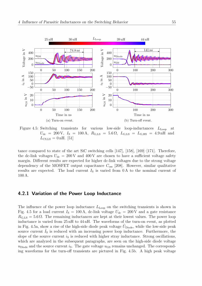
4 Influence of Parasitic Inductances on the Switching Behavior 55
25 nH 30 nH LLoop 39 nH 44 nH
0 50 100 150 200
0
200
400
Voltagein
V
uDS
uDiode
74.8 ns-
0 50 100 150 200−50
050
100150
i Sin
A
0 50 100 150 200
0
10
20
Time in ns
uGSin
V
(a) Turn-on event.
0 100 200 300
0
200
400
Voltagein
V
uDiode
uDS
141 ns -
0 100 200 300−50
050100150
i Sin
A
0 100 200 300
0
10
20
Time in ns
uGSin
V
(b) Turn-off event.
Figure 4.5: Switching transients for various low-side loop-inductances LLoop atUdc = 200 V, IS = 100 A, RG,LS = 5.6 Ω, LG,LS = LG,HS = 4.9 nH andLCS,LS = 0 nH. [51]
tance compared to state of the art SiC switching cells [147], [158], [169]–[171]. Therefore,the dc-link voltages Udc = 200 V and 400 V are chosen to have a sufficient voltage safetymargin. Different results are expected for higher dc-link voltages due to the strong voltagedependency of the MOSFET output capacitance Coss [208]. However, similar qualitativeresults are expected. The load current IS is varied from 0 A to the nominal current of100 A.
4.2.1 Variation of the Power Loop Inductance
The influence of the power loop inductance LLoop on the switching transients is shown inFig. 4.5 for a load current IS = 100 A, dc-link voltage Udc = 200 V and a gate resistanceRG,LS = 5.6 Ω. The remaining inductances are kept at their lowest values. The power loopinductance is varied from 25 nH to 44 nH. The waveforms of the turn-on event, as plottedin Fig. 4.5a, show a rise of the high-side diode peak voltage UDiode, while the low-side peaksource current IS is reduced with an increasing power loop inductance. Furthermore, theslope of the source current iS is reduced with higher stray inductance. Strong oscillations,which are analyzed in the subsequent paragraphs, are seen on the high-side diode voltageuDiode and the source current iS. The gate voltage uGS remains unchanged. The correspond-ing waveforms for the turn-off transients are pictured in Fig. 4.5b. A high peak voltage

56 4.2 Influence of the Parasitic Inductance on the Switching Transients
LLoop
Coss
Rds,on
ILoad
iS
uDS
uDiode
Udc
(a) Turn-on equivalent circuit.
LLoop
Coss
ILoad
iS
uDS
uDiode
Udc
(b) Turn-off equivalent circuit.
Figure 4.6: Equivalent circuit during the switching events.
UDS is observed (> 400 V) at the drain-source terminals of the low-side switch, followed bystrong oscillations. The same oscillation frequency is seen in the source current iS togetherwith a minor impact on the gate voltage uGS. For the sake of completeness, the remainingwaveforms of the switching transients using a dc-link voltage Udc = 200 V and 400 V anda gate resistance RG,LS = 0 Ω and 5.6 Ω are plotted in Fig. A.1, Fig. A.2 and Fig. A.3. Asimilar behavior is observed.
A possible explanation for the origin of the observed oscillations is given next. As the oscil-lations appear after the switching procedure is almost accomplished (uDS ≈ 0 V, Fig. 4.5a),equivalent circuits, as shown in Fig. 4.6, are developed. For the turn-on event, it is assumedthat the low-side switch is fully turned on and the diode instantly turns off at exactly thatmoment, as indicated by the opening of the high-side switch in Fig. 4.6a. A resonant tankformed by the power loop inductance LLoop and the output capacitance Coss of the high-sideswitch is seen. Analogously for the turn-off event, an equivalent circuit, which is valid forthe time after the diode voltage uDiode dropped to 0 V, is developed and shown in Fig. 4.6b.
The frequency of the observed oscillations f onosc and f off
osc following the turn-on and the turn-offevent from Fig. 4.5 are determined to 40.1 MHz and 42.6 MHz, respectively (see equa-tion (4.1) and equation (4.2)). This value matches well with the resonant frequency fres
formed by the output capacitance Coss = 350 pF [206, Fig. 17, Udc = 200 V] and the powerloop inductance LLoop = 44.1 nH, as shown by equation (4.3).
f onosc =
3
74.8 ns= 40.1 MHz (4.1)
f offosc =
6
140.8 ns= 42.6 MHz (4.2)
fres =1
2π√CossLLoop
= 40.5 MHz (4.3)
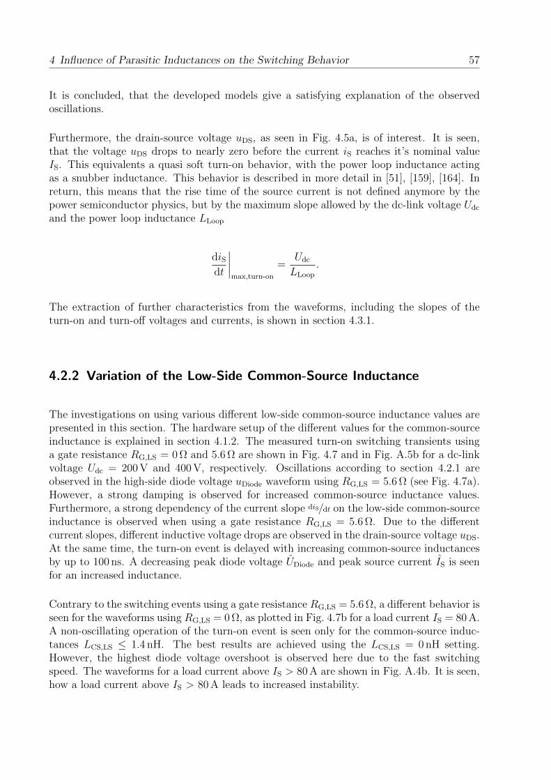
4 Influence of Parasitic Inductances on the Switching Behavior 57
It is concluded, that the developed models give a satisfying explanation of the observedoscillations.
Furthermore, the drain-source voltage uDS, as seen in Fig. 4.5a, is of interest. It is seen,that the voltage uDS drops to nearly zero before the current iS reaches it’s nominal valueIS. This equivalents a quasi soft turn-on behavior, with the power loop inductance actingas a snubber inductance. This behavior is described in more detail in [51], [159], [164]. Inreturn, this means that the rise time of the source current is not defined anymore by thepower semiconductor physics, but by the maximum slope allowed by the dc-link voltage Udc
and the power loop inductance LLoop
diSdt
∣∣∣∣max,turn-on
=Udc
LLoop
.
The extraction of further characteristics from the waveforms, including the slopes of theturn-on and turn-off voltages and currents, is shown in section 4.3.1.
4.2.2 Variation of the Low-Side Common-Source Inductance
The investigations on using various different low-side common-source inductance values arepresented in this section. The hardware setup of the different values for the common-sourceinductance is explained in section 4.1.2. The measured turn-on switching transients usinga gate resistance RG,LS = 0 Ω and 5.6 Ω are shown in Fig. 4.7 and in Fig. A.5b for a dc-linkvoltage Udc = 200 V and 400 V, respectively. Oscillations according to section 4.2.1 areobserved in the high-side diode voltage uDiode waveform using RG,LS = 5.6 Ω (see Fig. 4.7a).However, a strong damping is observed for increased common-source inductance values.Furthermore, a strong dependency of the current slope diS/dt on the low-side common-sourceinductance is observed when using a gate resistance RG,LS = 5.6 Ω. Due to the differentcurrent slopes, different inductive voltage drops are observed in the drain-source voltage uDS.At the same time, the turn-on event is delayed with increasing common-source inductancesby up to 100 ns. A decreasing peak diode voltage UDiode and peak source current IS is seenfor an increased inductance.
Contrary to the switching events using a gate resistance RG,LS = 5.6 Ω, a different behavior isseen for the waveforms using RG,LS = 0 Ω, as plotted in Fig. 4.7b for a load current IS = 80 A.A non-oscillating operation of the turn-on event is seen only for the common-source induc-tances LCS,LS ≤ 1.4 nH. The best results are achieved using the LCS,LS = 0 nH setting.However, the highest diode voltage overshoot is observed here due to the fast switchingspeed. The waveforms for a load current above IS > 80 A are shown in Fig. A.4b. It is seen,how a load current above IS > 80 A leads to increased instability.
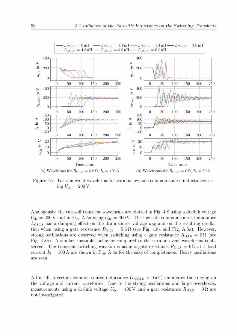
58 4.2 Influence of the Parasitic Inductance on the Switching Transients
LCS,LS = 0nH LCS,LS = 1.1 nH LCS,LS = 1.4 nH LCS,LS = 3.0 nHLCS,LS = 4.3 nH LCS,LS = 5.6 nH LCS,LS = 6.5 nH
0 50 100 150 200 250
0
200
400
uDSin
V
0 50 100 150 200 250
0
200
400
uDiodein
V
0 50 100 150 200 250−50
050100150
i Sin
A
0 50 100 150 200 250
0
10
20
Time in ns
uGSin
V
(a) Waveforms for RG,LS = 5.6 Ω, IS = 100 A
0 50 100 150 200 250
0
200
400
uDSin
V
0 50 100 150 200 250
0
200
400
uDiodein
V0 50 100 150 200 250
−50050100150
i Sin
A
0 50 100 150 200 250
0
10
20
Time in ns
uGSin
V
(b) Waveforms for RG,LS = 0 Ω, IS = 80 A
Figure 4.7: Turn-on event waveforms for various low-side common-source inductances us-ing Udc = 200 V.
Analogously, the turn-off transient waveforms are plotted in Fig. 4.8 using a dc-link voltageUdc = 200 V and in Fig. A.5a using Udc = 400 V. The low-side common-source inductanceLCS,LS has a damping effect on the drain-source voltage uDS and on the resulting oscilla-tion when using a gate resistance RG,LS = 5.6 Ω (see Fig. 4.8a and Fig. A.5a). However,strong oscillations are observed when switching using a gate resistance RG,LS = 0 Ω (seeFig. 4.8b). A similar, unstable, behavior compared to the turn-on event waveforms is ob-served. The transient switching waveforms using a gate resistance RG,LS = 0 Ω at a loadcurrent IS = 100 A are shown in Fig. A.4a for the sake of completeness. Heavy oscillationsare seen.
All in all, a certain common-source inductance (LCS,LS > 0 nH) eliminates the ringing onthe voltage and current waveforms. Due to the strong oscillations and large overshoots,measurements using a dc-link voltage Udc = 400 V and a gate resistance RG,LS = 0 Ω arenot investigated.

4 Influence of Parasitic Inductances on the Switching Behavior 59
LCS,LS = 0nH LCS,LS = 1.1 nH LCS,LS = 1.4 nH LCS,LS = 3.0 nHLCS,LS = 4.3 nH LCS,LS = 5.6 nH LCS,LS = 6.5 nH
0 100 200 300
0
500
uDSin
V
0 100 200 300−100
0
100
200
uDiodein
V
0 100 200 300
−50050100
i Sin
A
0 100 200 300
−1001020
Time in ns
uGSin
V
(a) Waveforms at RG,LS = 5.6 Ω, IS = 100 A.
0 100 200 300
0
500
uDSin
V
0 100 200 300−100
0
100
200
uDiodein
V
0 100 200 300
−50050100
i Sin
A
0 100 200 300
−1001020
Time in ns
uGSin
V
(b) Waveforms at RG,LS = 0 Ω, IS = 80 A.
Figure 4.8: Turn-off event waveforms for various low-side common-source inductances us-ing Udc = 200 V.
4.2.3 Variation of the High-Side Common-Source Inductance
A variation of the high-side common-source inductance while switching the low-side switchis expected to act as a variation of the power loop inductance LLoop. The correspondingwaveforms are plotted in Fig. A.6, Fig. A.7, Fig. A.8 and Fig. A.9 using a gate resistanceRG,LS = 0 Ω and 5.6 Ω and a dc-link voltage Udc = 200 V and 400 V. Only a minor influ-ence on the high-side diode voltage is observed, which seems to differ from the power loopinfluence. Section 4.3.3 gives a more detailed evaluation.
4.2.4 Variation of the Low-Side Gate Inductance
Literature [209] shows that the gate inductance is the source for oscillations, if the criteriafrom equation (4.4) matches. Inversely, a minimum gate inductance according to equa-tion (4.5) is defined above which gate oscillations are appearing. In the given setup, a gate
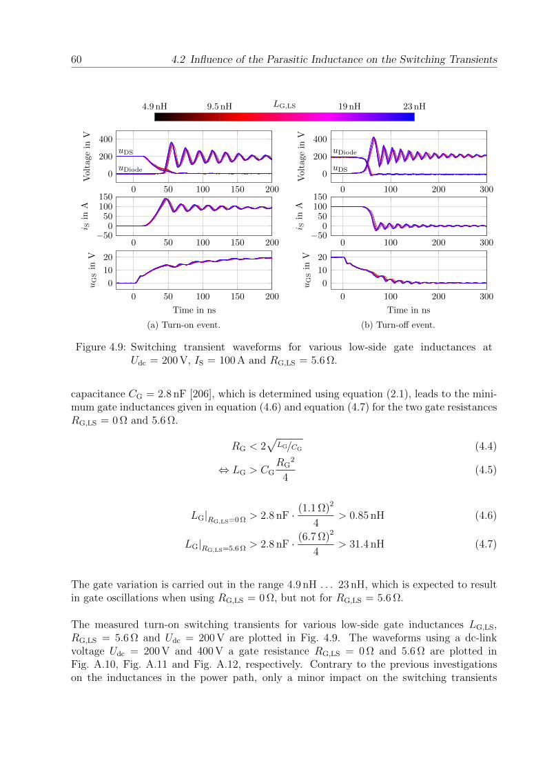
60 4.2 Influence of the Parasitic Inductance on the Switching Transients
4.9 nH 9.5 nH LG,LS 19 nH 23 nH
0 50 100 150 200
0
200
400
Voltagein
V
uDS
uDiode
0 50 100 150 200−50
050
100150
i Sin
A
0 50 100 150 200
0
10
20
Time in ns
uGSin
V
(a) Turn-on event.
0 100 200 300
0
200
400
Voltagein
V
uDiode
uDS
0 100 200 300−50
050100150
i Sin
A0 100 200 300
0
10
20
Time in nsuGSin
V
(b) Turn-off event.
Figure 4.9: Switching transient waveforms for various low-side gate inductances atUdc = 200 V, IS = 100 A and RG,LS = 5.6 Ω.
capacitance CG = 2.8 nF [206], which is determined using equation (2.1), leads to the mini-mum gate inductances given in equation (4.6) and equation (4.7) for the two gate resistancesRG,LS = 0 Ω and 5.6 Ω.
RG < 2√
LG/CG (4.4)
⇔ LG > CGRG
2
4(4.5)
LG|RG,LS=0 Ω > 2.8 nF · (1.1 Ω)2
4> 0.85 nH (4.6)
LG|RG,LS=5.6 Ω > 2.8 nF · (6.7 Ω)2
4> 31.4 nH (4.7)
The gate variation is carried out in the range 4.9 nH . . . 23 nH, which is expected to resultin gate oscillations when using RG,LS = 0 Ω, but not for RG,LS = 5.6 Ω.
The measured turn-on switching transients for various low-side gate inductances LG,LS,RG,LS = 5.6 Ω and Udc = 200 V are plotted in Fig. 4.9. The waveforms using a dc-linkvoltage Udc = 200 V and 400 V a gate resistance RG,LS = 0 Ω and 5.6 Ω are plotted inFig. A.10, Fig. A.11 and Fig. A.12, respectively. Contrary to the previous investigationson the inductances in the power path, only a minor impact on the switching transients
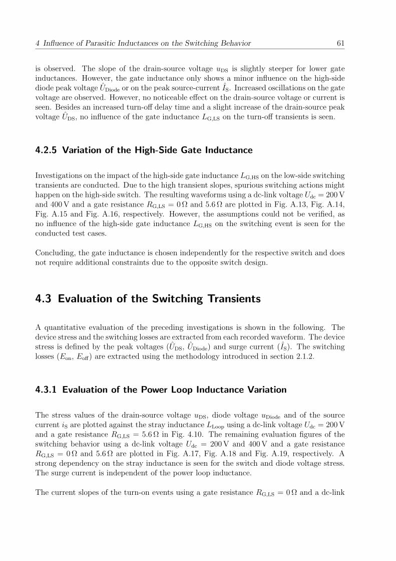
4 Influence of Parasitic Inductances on the Switching Behavior 61
is observed. The slope of the drain-source voltage uDS is slightly steeper for lower gateinductances. However, the gate inductance only shows a minor influence on the high-sidediode peak voltage UDiode or on the peak source-current IS. Increased oscillations on the gatevoltage are observed. However, no noticeable effect on the drain-source voltage or current isseen. Besides an increased turn-off delay time and a slight increase of the drain-source peakvoltage UDS, no influence of the gate inductance LG,LS on the turn-off transients is seen.
4.2.5 Variation of the High-Side Gate Inductance
Investigations on the impact of the high-side gate inductance LG,HS on the low-side switchingtransients are conducted. Due to the high transient slopes, spurious switching actions mighthappen on the high-side switch. The resulting waveforms using a dc-link voltage Udc = 200 Vand 400 V and a gate resistance RG,LS = 0 Ω and 5.6 Ω are plotted in Fig. A.13, Fig. A.14,Fig. A.15 and Fig. A.16, respectively. However, the assumptions could not be verified, asno influence of the high-side gate inductance LG,HS on the switching event is seen for theconducted test cases.
Concluding, the gate inductance is chosen independently for the respective switch and doesnot require additional constraints due to the opposite switch design.
4.3 Evaluation of the Switching Transients
A quantitative evaluation of the preceding investigations is shown in the following. Thedevice stress and the switching losses are extracted from each recorded waveform. The devicestress is defined by the peak voltages (UDS, UDiode) and surge current (IS). The switchinglosses (Eon, Eoff) are extracted using the methodology introduced in section 2.1.2.
4.3.1 Evaluation of the Power Loop Inductance Variation
The stress values of the drain-source voltage uDS, diode voltage uDiode and of the sourcecurrent iS are plotted against the stray inductance LLoop using a dc-link voltage Udc = 200 Vand a gate resistance RG,LS = 5.6 Ω in Fig. 4.10. The remaining evaluation figures of theswitching behavior using a dc-link voltage Udc = 200 V and 400 V and a gate resistanceRG,LS = 0 Ω and 5.6 Ω are plotted in Fig. A.17, Fig. A.18 and Fig. A.19, respectively. Astrong dependency on the stray inductance is seen for the switch and diode voltage stress.The surge current is independent of the power loop inductance.
The current slopes of the turn-on events using a gate resistance RG,LS = 0 Ω and a dc-link
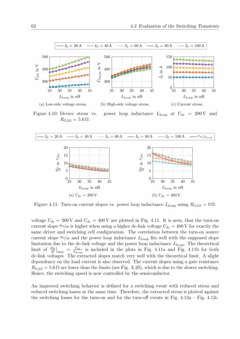
62 4.3 Evaluation of the Switching Transients
IS = 20A IS = 40A IS = 60A IS = 80A IS = 100A
25 30 35 40 45
300
400
500
LLoop in nH
UDSin
V
(a) Low-side voltage stress.
25 30 35 40 45
300
400
500
LLoop in nHUDiodein
V
(b) High-side voltage stress.
25 30 35 40 450
50
100
150
LLoop in nH
I Sin
A
(c) Current stress.
Figure 4.10: Device stress vs. power loop inductance LLoop at Udc = 200 V andRG,LS = 5.6 Ω.
IS = 20A IS = 40A IS = 60A IS = 80A IS = 100A Udc/LLoop
25 30 35 40 450
5
10
15
20
LLoop in nH
di S dtin
A/n
s
(a) Udc = 200 V.
25 30 35 40 450
5
10
15
20
LLoop in nH
di S dtin
A/n
s
(b) Udc = 400 V.
Figure 4.11: Turn-on current slopes vs. power loop inductance LLoop using RG,LS = 0 Ω.
voltage Udc = 200 V and Udc = 400 V are plotted in Fig. 4.11. It is seen, that the turn-oncurrent slope diS/dt is higher when using a higher dc-link voltage Udc = 400 V for exactly thesame driver and switching cell configuration. The correlation between the turn-on sourcecurrent slope diS/dt and the power loop inductance LLoop fits well with the supposed slopelimitation due to the dc-link voltage and the power loop inductance LLoop. The theoreticallimit of diS
dt
∣∣max
= Udc
LLoopis included in the plots in Fig. 4.11a and Fig. 4.11b for both
dc-link voltages. The extracted slopes match very well with the theoretical limit. A slightdependency on the load current is also observed. The current slopes using a gate resistanceRG,LS = 5.6 Ω are lower than the limits (see Fig. A.20), which is due to the slower switching.Hence, the switching speed is now controlled by the semiconductor.
An improved switching behavior is defined for a switching event with reduced stress andreduced switching losses at the same time. Therefore, the extracted stress is plotted againstthe switching losses for the turn-on and for the turn-off events in Fig. 4.12a – Fig. 4.12c.
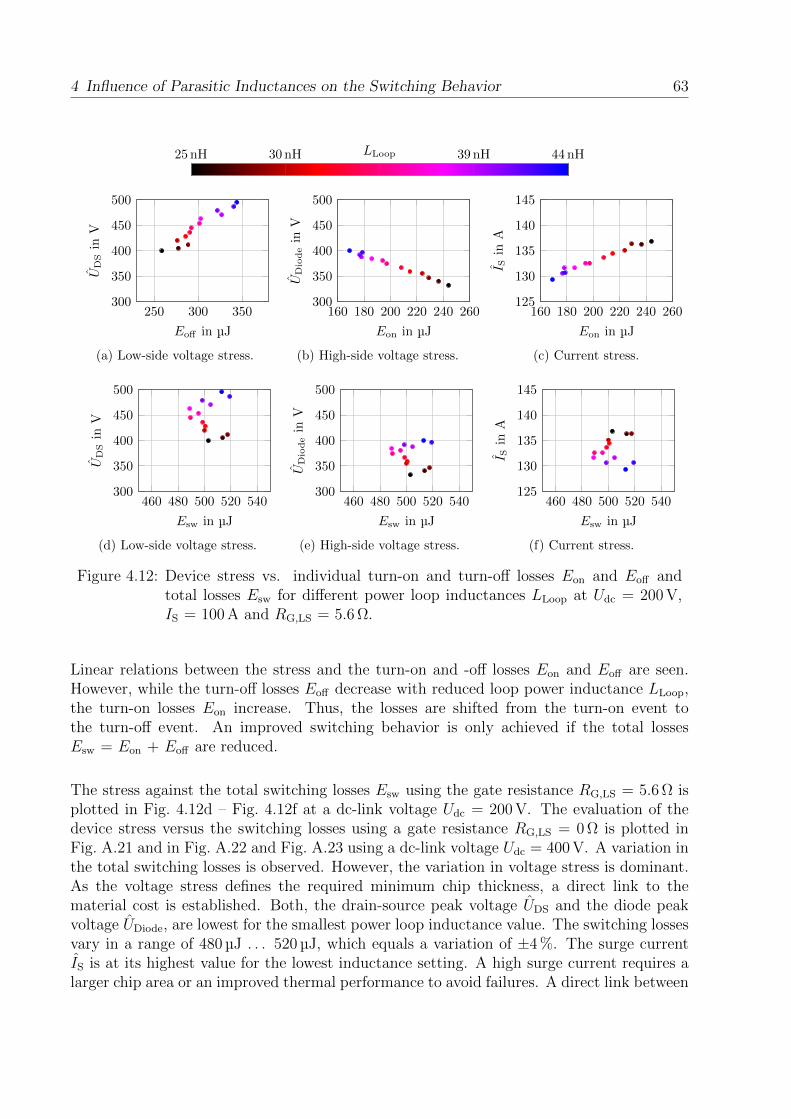
4 Influence of Parasitic Inductances on the Switching Behavior 63
25 nH 30 nH LLoop 39 nH 44 nH
250 300 350300
350
400
450
500
Eoff in µJ
UD
Sin
V
(a) Low-side voltage stress.
160 180 200 220 240 260300
350
400
450
500
Eon in µJ
UDiodein
V
(b) High-side voltage stress.
160 180 200 220 240 260125
130
135
140
145
Eon in µJ
I Sin
A
(c) Current stress.
460 480 500 520 540300
350
400
450
500
Esw in µJ
UDSin
V
(d) Low-side voltage stress.
460 480 500 520 540300
350
400
450
500
Esw in µJ
UDiodein
V
(e) High-side voltage stress.
460 480 500 520 540125
130
135
140
145
Esw in µJ
I Sin
A
(f) Current stress.
Figure 4.12: Device stress vs. individual turn-on and turn-off losses Eon and Eoff andtotal losses Esw for different power loop inductances LLoop at Udc = 200 V,IS = 100 A and RG,LS = 5.6 Ω.
Linear relations between the stress and the turn-on and -off losses Eon and Eoff are seen.However, while the turn-off losses Eoff decrease with reduced loop power inductance LLoop,the turn-on losses Eon increase. Thus, the losses are shifted from the turn-on event tothe turn-off event. An improved switching behavior is only achieved if the total lossesEsw = Eon + Eoff are reduced.
The stress against the total switching losses Esw using the gate resistance RG,LS = 5.6 Ω isplotted in Fig. 4.12d – Fig. 4.12f at a dc-link voltage Udc = 200 V. The evaluation of thedevice stress versus the switching losses using a gate resistance RG,LS = 0 Ω is plotted inFig. A.21 and in Fig. A.22 and Fig. A.23 using a dc-link voltage Udc = 400 V. A variation inthe total switching losses is observed. However, the variation in voltage stress is dominant.As the voltage stress defines the required minimum chip thickness, a direct link to thematerial cost is established. Both, the drain-source peak voltage UDS and the diode peakvoltage UDiode, are lowest for the smallest power loop inductance value. The switching lossesvary in a range of 480 µJ . . . 520 µJ, which equals a variation of ±4 %. The surge currentIS is at its highest value for the lowest inductance setting. A high surge current requires alarger chip area or an improved thermal performance to avoid failures. A direct link between
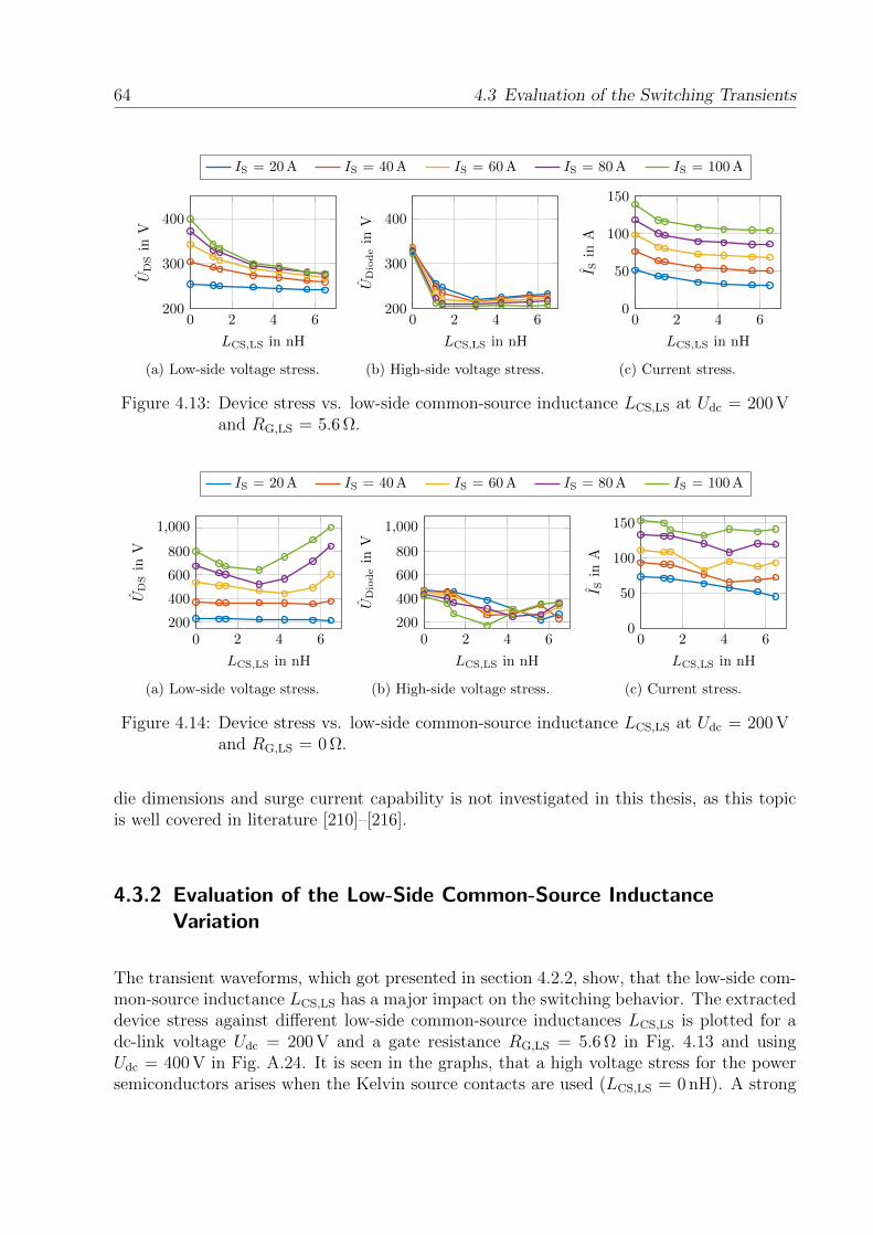
64 4.3 Evaluation of the Switching Transients
IS = 20A IS = 40A IS = 60A IS = 80A IS = 100A
0 2 4 6200
300
400
LCS,LS in nH
UDSin
V
(a) Low-side voltage stress.
0 2 4 6200
300
400
LCS,LS in nH
UDiodein
V(b) High-side voltage stress.
0 2 4 60
50
100
150
LCS,LS in nH
I Sin
A
(c) Current stress.
Figure 4.13: Device stress vs. low-side common-source inductance LCS,LS at Udc = 200 Vand RG,LS = 5.6 Ω.
IS = 20A IS = 40A IS = 60A IS = 80A IS = 100A
0 2 4 6200
400
600
800
1,000
LCS,LS in nH
UDSin
V
(a) Low-side voltage stress.
0 2 4 6200
400
600
800
1,000
LCS,LS in nH
UDiodein
V
(b) High-side voltage stress.
0 2 4 60
50
100
150
LCS,LS in nH
I Sin
A
(c) Current stress.
Figure 4.14: Device stress vs. low-side common-source inductance LCS,LS at Udc = 200 Vand RG,LS = 0 Ω.
die dimensions and surge current capability is not investigated in this thesis, as this topicis well covered in literature [210]–[216].
4.3.2 Evaluation of the Low-Side Common-Source InductanceVariation
The transient waveforms, which got presented in section 4.2.2, show, that the low-side com-mon-source inductance LCS,LS has a major impact on the switching behavior. The extracteddevice stress against different low-side common-source inductances LCS,LS is plotted for adc-link voltage Udc = 200 V and a gate resistance RG,LS = 5.6 Ω in Fig. 4.13 and usingUdc = 400 V in Fig. A.24. It is seen in the graphs, that a high voltage stress for the powersemiconductors arises when the Kelvin source contacts are used (LCS,LS = 0 nH). A strong
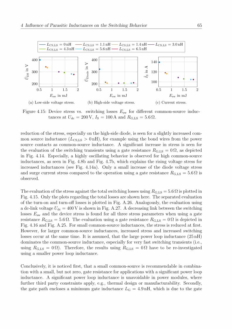
4 Influence of Parasitic Inductances on the Switching Behavior 65
LCS,LS = 0nH LCS,LS = 1.1 nH LCS,LS = 1.4 nH LCS,LS = 3.0 nHLCS,LS = 4.3 nH LCS,LS = 5.6 nH LCS,LS = 6.5 nH
0.5 1 1.5 2
200
300
400
Esw in mJ
UDSin
V
(a) Low-side voltage stress.
0.5 1 1.5 2
200
300
400
Esw in mJ
UDiodein
V
(b) High-side voltage stress.
0.5 1 1.5 2
100
120
140
Esw in mJ
I Sin
A
(c) Current stress.
Figure 4.15: Device stress vs. switching losses Esw for different common-source induc-tances at Udc = 200 V, IS = 100 A and RG,LS = 5.6 Ω.
reduction of the stress, especially on the high-side diode, is seen for a slightly increased com-mon source inductance (LCS,LS > 0 nH), for example using the bond wires from the powersource contacts as common-source inductance. A significant increase in stress is seen forthe evaluation of the switching transients using a gate resistance RG,LS = 0 Ω, as depictedin Fig. 4.14. Especially, a highly oscillating behavior is observed for high common-sourceinductances, as seen in Fig. 4.8b and Fig. 4.7b, which explains the rising voltage stress forincreased inductances (see Fig. 4.14a). Only a small increase of the diode voltage stressand surge current stress compared to the operation using a gate resistance RG,LS = 5.6 Ω isobserved.
The evaluation of the stress against the total switching losses usingRG,LS = 5.6 Ω is plotted inFig. 4.15. Only the plots regarding the total losses are shown here. The separated evaluationof the turn-on and turn-off losses is plotted in Fig. A.26. Analogously, the evaluation usinga dc-link voltage Udc = 400 V is shown in Fig. A.27. A decreasing link between the switchinglosses Esw and the device stress is found for all three stress parameters when using a gateresistance RG,LS = 5.6 Ω. The evaluation using a gate resistance RG,LS = 0 Ω is depicted inFig. 4.16 and Fig. A.25. For small common-source inductances, the stress is reduced at first.However, for larger common-source inductances, increased stress and increased switchinglosses occur at the same time. It is assumed, that the large power loop inductance (25 nH)dominates the common-source inductance, especially for very fast switching transients (i.e.,using RG,LS = 0 Ω). Therefore, the results using RG,LS = 0 Ω have to be re-investigatedusing a smaller power loop inductance.
Conclusively, it is noticed first, that a small common-source is recommendable in combina-tion with a small, but not zero, gate resistance for applications with a significant power loopinductance. A significant power loop inductance is unavoidable in power modules, wherefurther third party constraints apply, e.g., thermal design or manufacturability. Secondly,the gate path encloses a minimum gate inductance LG = 4.9 nH, which is due to the gate
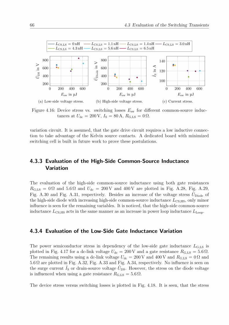
66 4.3 Evaluation of the Switching Transients
LCS,LS = 0nH LCS,LS = 1.1 nH LCS,LS = 1.4 nH LCS,LS = 3.0 nHLCS,LS = 4.3 nH LCS,LS = 5.6 nH LCS,LS = 6.5 nH
0 200 400 600200
400
600
800
Esw in µJ
UDSin
V
(a) Low-side voltage stress.
0 200 400 600200
400
600
800
Esw in µJUDiodein
V
(b) High-side voltage stress.
0 200 400 600
100
120
140
Esw in µJ
I Sin
A
(c) Current stress.
Figure 4.16: Device stress vs. switching losses Esw for different common-source induc-tances at Udc = 200 V, IS = 80 A, RG,LS = 0 Ω.
variation circuit. It is assumed, that the gate drive circuit requires a low inductive connec-tion to take advantage of the Kelvin source contacts. A dedicated board with minimizedswitching cell is built in future work to prove these postulations.
4.3.3 Evaluation of the High-Side Common-Source InductanceVariation
The evaluation of the high-side common-source inductance using both gate resistancesRG,LS = 0 Ω and 5.6 Ω and Udc = 200 V and 400 V are plotted in Fig. A.28, Fig. A.29,
Fig. A.30 and Fig. A.31, respectively. Besides an increase of the voltage stress UDiode ofthe high-side diode with increasing high-side common-source inductance LCS,HS, only minorinfluence is seen for the remaining variables. It is noticed, that the high-side common-sourceinductance LCS,HS acts in the same manner as an increase in power loop inductance LLoop.
4.3.4 Evaluation of the Low-Side Gate Inductance Variation
The power semiconductor stress in dependency of the low-side gate inductance LG,LS isplotted in Fig. 4.17 for a dc-link voltage Udc = 200 V and a gate resistance RG,LS = 5.6 Ω.The remaining results using a dc-link voltage Udc = 200 V and 400 V and RG,LS = 0 Ω and5.6 Ω are plotted in Fig. A.32, Fig. A.33 and Fig. A.34, respectively. No influence is seen onthe surge current IS or drain-source voltage UDS. However, the stress on the diode voltageis influenced when using a gate resistance RG,LS = 5.6 Ω.
The device stress versus switching losses is plotted in Fig. 4.18. It is seen, that the stress

4 Influence of Parasitic Inductances on the Switching Behavior 67
IS = 20A IS = 40A IS = 60A IS = 80A IS = 100A
5 10 15 20200
300
400
LG,LS in nH
UDSin
V
(a) Low-side voltage stress.
5 10 15 20200
300
400
LG,LS in nHUDiodein
V
(b) High-side voltage stress.
5 10 15 200
50
100
150
LG,LS in nH
I Sin
A
(c) Current stress.
Figure 4.17: Device stress vs. low-side gate ind. LG,LS at Udc = 200 V and RG,LS = 5.6 Ω.
4.9 nH 9.5 nH LG,LS 19 nH 23 nH
400 450 500 550300
350
400
450
Esw in µJ
UDSin
V
(a) Low-side voltage stress.
440 460 480 500 520300
350
400
450
Esw in µJ
UDiodein
V
(b) High-side voltage stress.
440 460 480 500 520130
135
140
145
150
Esw in µJ
I Sin
A
(c) Current stress.
Figure 4.18: Device stress vs. switching losses Esw for different low-side gate inductancesLG,LS at Udc = 200 V, IS = 100 A and RG,LS = 5.6 Ω.
reduction is linked linearly with an increase in switching losses. The evaluation againstseparated turn-on and turn-off losses is plotted in Fig. A.35. The remaining plots usingUdc = 400 V and RG,LS = 0 Ω and 5.6 Ω are shown in Fig. A.36, Fig. A.37 and A.38. Unlikefor the fast switching actions (RG,LS = 0 Ω), a clean dependency is seen for the switchingactions using RG,LS = 5.6 Ω.
4.3.5 Evaluation of the High-Side Gate Inductance Variation
As already presumed in section 4.2.5, no influence of the high-side side gate inductance onthe low-side switching behavior is observed. For the sake of completeness, the evaluationresults using a dc-link voltage Udc = 200 V and 400 V, a high-side gate resistance RG,HS = 0 Ωand a low-side gate resistance RG,LS = 0 Ω and 5.6 Ω are plotted in Fig. A.39, Fig. A.40,Fig. A.41 and Fig. A.42.
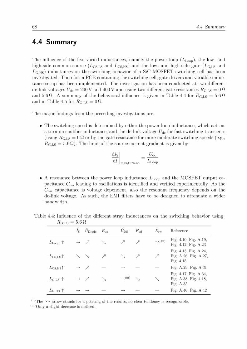
68 4.4 Summary
4.4 Summary
The influence of the five varied inductances, namely the power loop (LLoop), the low- andhigh-side common-source (LCS,LS and LCS,HS) and the low- and high-side gate (LG,LS andLG,HS) inductances on the switching behavior of a SiC MOSFET switching cell has beeninvestigated. Therefor, a PCB containing the switching cell, gate drivers and variable induc-tance setup has been implemented. The investigation has been conducted at two differentdc-link voltages Udc = 200 V and 400 V and using two different gate resistances RG,LS = 0 Ωand 5.6 Ω. A summary of the behavioral influence is given in Table 4.4 for RG,LS = 5.6 Ωand in Table 4.5 for RG,LS = 0 Ω.
The major findings from the preceding investigations are:
• The switching speed is determined by either the power loop inductance, which acts asa turn-on snubber inductance, and the dc-link voltage Udc for fast switching transients(using RG,LS = 0 Ω or by the gate resistance for more moderate switching speeds (e.g.,RG,LS = 5.6 Ω). The limit of the source current gradient is given by
diSdt
∣∣∣∣max,turn-on
=Udc
LLoop
• A resonance between the power loop inductance LLoop and the MOSFET output ca-pacitance Coss leading to oscillations is identified and verified experimentally. As theCoss capacitance is voltage dependent, also the resonant frequency depends on thedc-link voltage. As such, the EMI filters have to be designed to attenuate a widerbandwidth.
Table 4.4: Influence of the different stray inductances on the switching behavior usingRG,LS = 5.6 Ω
IS UDiode Eon UDS Eoff Esw Reference
LLoop ↑ → (ii) Fig. 4.10, Fig. A.19,Fig. 4.12, Fig. A.23
LCS,LS↑ Fig. 4.13, Fig. A.24,Fig. A.26, Fig. A.27,Fig. 4.15
LCS,HS↑ → — → — — Fig. A.29, Fig. A.31
LG,LS ↑ → →(iii) Fig. 4.17, Fig. A.34,Fig. A.38, Fig. 4.18,Fig. A.35
LG,HS ↑ → → — → — — Fig. A.40, Fig. A.42
(ii)The arrow stands for a jittering of the results, no clear tendency is recognizable.(iii)Only a slight decrease is noticed.

4 Influence of Parasitic Inductances on the Switching Behavior 69
Table 4.5: Influence of the different stray inductances on the switching behavior usingRG,LS = 0 Ω
IS UDiode Eon UDS Eoff Esw Reference
LLoop ↑ → (200V)
(400V)
(200V)
(400V)
Fig. A.17, Fig. A.18,Fig. A.21, Fig. A.22
LCS,LS↑ → → Fig. 4.14, Fig. A.25,Fig. 4.16
LCS,HS↑ → — → — — Fig. A.28, Fig. A.30
LG,LS ↑ → → → Fig. A.32, Fig. A.33,Fig. A.36, Fig. A.37
LG,HS ↑ → → — → — — Fig. A.39, Fig. A.41
Concerning the individual parasitic inductances, the following key aspects are retained:
• Power loop inductance LLoop: A linear link between the stress and the inductance isestablished while the total switching losses remain unchanged. Thus, the power loopinductance effects only the device stress without impact on the total switching losses.However, the individual turn-on losses are shifted to the turn-off losses and vice versa.
• Low-side common-source inductance LCS,LS: Instabilities are observed depending onthe gate resistance and the common-source inductance. A careful choice betweenKelvin source contact and Kelvin power source contact (including power source bondwires) has to be taken because oscillations got determined in combination with a smalland larger gate resistance. In fact, a small common-source inductance dampens theringing when switching with a gate resistance RG,LS = 5.6 Ω.
• High-side common-source inductance LCS,HS: Acts as an additional power loop induc-tance regarding low-side switching.
• Low-side gate inductance LG,LS: Lower switching losses for higher gate inductanceLG,LS are found in combination with a gate resistance RG,LS = 5.6 Ω. The lossesremain more or less unchanged for faster switching events (e.g., RG,LS = 0 Ω). Thelowest stress on the drain-source voltage uDS is found for low inductance values, whichenforces that a compromise has to be found between stress and switching losses.
• High-side gate inductance LG,HS: No noticeable influence on the low-side switching isobserved, which means that the gate inductance is designed according to the require-ments of the corresponding switch only.

70

5 Influencing Switching Transients using ActiveGate Drivers
Besides the influence of the parasitic elements around the switching cell, the power semi-conductor gate driver has a major impact on the switching transients [28], [29] (see alsosection 2.2). Influencing the switching behavior of power semiconductors to reduce theswitching losses and/or to reduce the device stress has a positive impact on the total costand efficiency of the power electronics converter. Furthermore, it is shown in literature,that the switching transients can be positively influenced using various different passive andAGD topologies. Furthermore, it is shown that the transient switching behavior dependson either the gate voltage or gate current profile rather than on the gate driver topologyitself. The topology only represents an approach on how to impress a certain gate profile.It is indifferent whether a voltage source or current source gate driver topology is chosenfor equal switching behavior as it is shown in [94].
This chapter outlines how much the stress of a power semiconductor can be influencedduring the switching transient and what are the additional costs in losses. Therefore, anAGD topology, which is able to set any desired gate profile, is introduced. A voltagesource, stage-wise switched resistor AGD topology is chosen as a universal gate driver for thefollowing investigations. To cover a broad range of power semiconductors and applications,the investigations are conducted for an non-punch-through (NPT) IGBT power module anda SiC MOSFET (Cree CPM2-1200-0040B) switching cell. The characteristic values of theemployed power devices are shown in Table 5.1.
Due to a large difference in switching times of Si IGBTs and SiC MOSFET power semicon-ductors, two separate gate drivers are implemented. The switching times of SiC MOSFETsare at least a decade faster compared to Si IGBTs [90]. A detailed investigation on theinfluence of the switching transients is conducted for both drivers. The chapter closes witha summary on the achievable gain and which parameters need tuning to achieve a certainperformance.
Table 5.1: Characteristic values of used devices
IGBT SiC MOSFET
Blocking voltage 800 V 1200 VNominal current 2 × 300 A 63 AGeneration IGBT2 (NPT) [65] 2nd
71
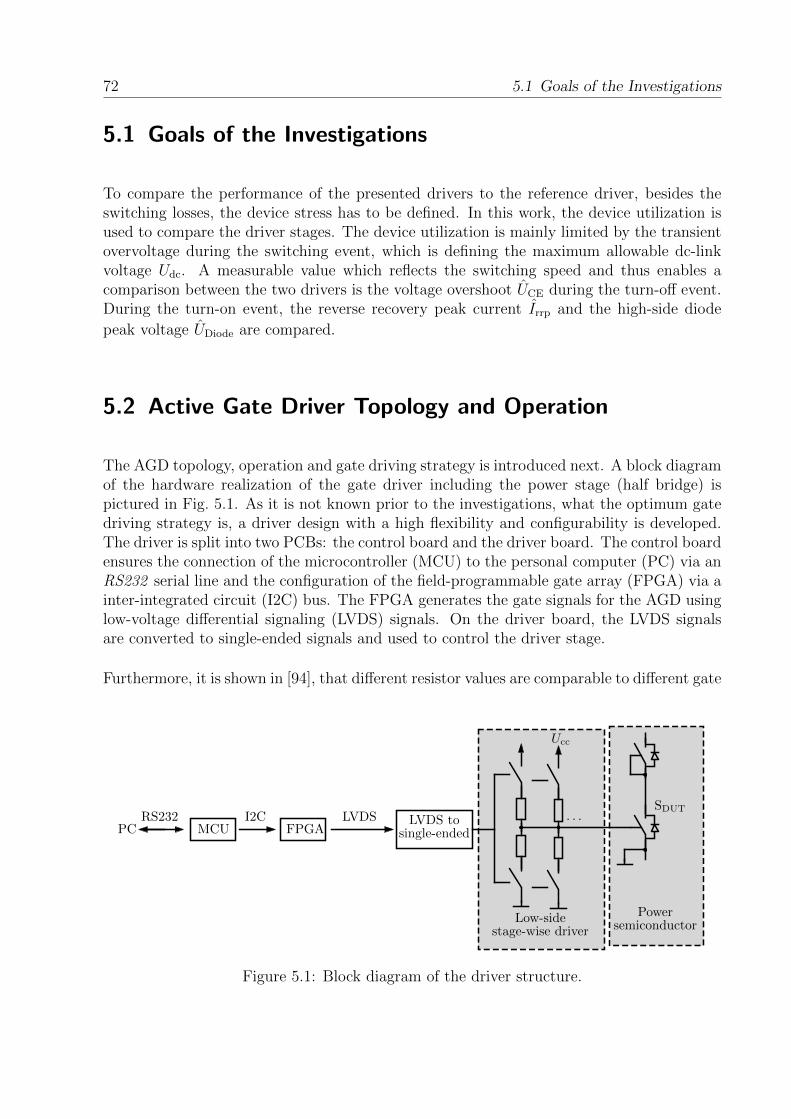
72 5.1 Goals of the Investigations
5.1 Goals of the Investigations
To compare the performance of the presented drivers to the reference driver, besides theswitching losses, the device stress has to be defined. In this work, the device utilization isused to compare the driver stages. The device utilization is mainly limited by the transientovervoltage during the switching event, which is defining the maximum allowable dc-linkvoltage Udc. A measurable value which reflects the switching speed and thus enables acomparison between the two drivers is the voltage overshoot UCE during the turn-off event.During the turn-on event, the reverse recovery peak current Irrp and the high-side diode
peak voltage UDiode are compared.
5.2 Active Gate Driver Topology and Operation
The AGD topology, operation and gate driving strategy is introduced next. A block diagramof the hardware realization of the gate driver including the power stage (half bridge) ispictured in Fig. 5.1. As it is not known prior to the investigations, what the optimum gatedriving strategy is, a driver design with a high flexibility and configurability is developed.The driver is split into two PCBs: the control board and the driver board. The control boardensures the connection of the microcontroller (MCU) to the personal computer (PC) via anRS232 serial line and the configuration of the field-programmable gate array (FPGA) via ainter-integrated circuit (I2C) bus. The FPGA generates the gate signals for the AGD usinglow-voltage differential signaling (LVDS) signals. On the driver board, the LVDS signalsare converted to single-ended signals and used to control the driver stage.
Furthermore, it is shown in [94], that different resistor values are comparable to different gate
MCU FPGAPCRS232 LVDSI2C LVDS to
single-ended
Low-sidestage-wise driver
Powersemiconductor
. . .SDUT
Ucc
Figure 5.1: Block diagram of the driver structure.
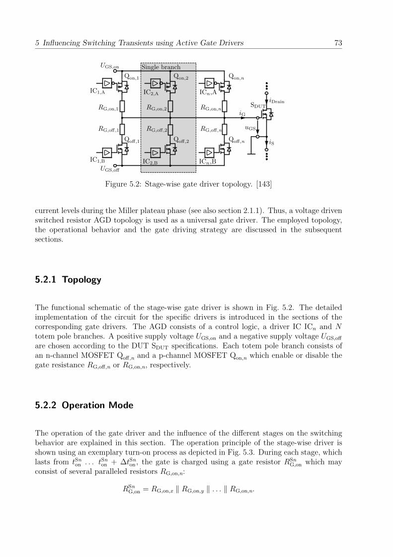
5 Influencing Switching Transients using Active Gate Drivers 73
UGS,on
UGS,off
RG,on,1
Qoff,1
uGS
SDUTiDrain
iG
Qon,1
RG,on,2 RG,on,n
RG,off,2 RG,off,nRG,off,1
Qoff,2 Qoff,n
Qon,2 Qon,n
IC1,B
IC1,A IC2,A ICn,A
IC2,B ICn,B
iS
Single branch
Figure 5.2: Stage-wise gate driver topology. [143]
current levels during the Miller plateau phase (see also section 2.1.1). Thus, a voltage drivenswitched resistor AGD topology is used as a universal gate driver. The employed topology,the operational behavior and the gate driving strategy are discussed in the subsequentsections.
5.2.1 Topology
The functional schematic of the stage-wise gate driver is shown in Fig. 5.2. The detailedimplementation of the circuit for the specific drivers is introduced in the sections of thecorresponding gate drivers. The AGD consists of a control logic, a driver IC ICn and Ntotem pole branches. A positive supply voltage UGS,on and a negative supply voltage UGS,off
are chosen according to the DUT SDUT specifications. Each totem pole branch consists ofan n-channel MOSFET Qoff,n and a p-channel MOSFET Qon,n which enable or disable thegate resistance RG,off,n or RG,on,n, respectively.
5.2.2 Operation Mode
The operation of the gate driver and the influence of the different stages on the switchingbehavior are explained in this section. The operation principle of the stage-wise driver isshown using an exemplary turn-on process as depicted in Fig. 5.3. During each stage, whichlasts from tSnon . . . tSnon + ∆tSnon , the gate is charged using a gate resistor RSn
G,on which mayconsist of several paralleled resistors RG,on,n:
RSnG,on = RG,on,x ‖ RG,on,y ‖ . . . ‖ RG,on,n.
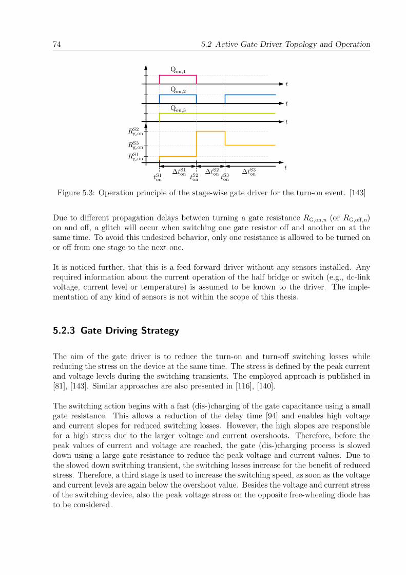
74 5.2 Active Gate Driver Topology and Operation
Qon,1
Qon,2
Qon,3
RS1g,on
RS3g,on
RS2g,on
∆tS1on ∆tS2on ∆tS3ont
t
t
t
tS1on tS2on tS3on
Figure 5.3: Operation principle of the stage-wise gate driver for the turn-on event. [143]
Due to different propagation delays between turning a gate resistance RG,on,n (or RG,off,n)on and off, a glitch will occur when switching one gate resistor off and another on at thesame time. To avoid this undesired behavior, only one resistance is allowed to be turned onor off from one stage to the next one.
It is noticed further, that this is a feed forward driver without any sensors installed. Anyrequired information about the current operation of the half bridge or switch (e.g., dc-linkvoltage, current level or temperature) is assumed to be known to the driver. The imple-mentation of any kind of sensors is not within the scope of this thesis.
5.2.3 Gate Driving Strategy
The aim of the gate driver is to reduce the turn-on and turn-off switching losses whilereducing the stress on the device at the same time. The stress is defined by the peak currentand voltage levels during the switching transients. The employed approach is published in[81], [143]. Similar approaches are also presented in [116], [140].
The switching action begins with a fast (dis-)charging of the gate capacitance using a smallgate resistance. This allows a reduction of the delay time [94] and enables high voltageand current slopes for reduced switching losses. However, the high slopes are responsiblefor a high stress due to the larger voltage and current overshoots. Therefore, before thepeak values of current and voltage are reached, the gate (dis-)charging process is sloweddown using a large gate resistance to reduce the peak voltage and current values. Due tothe slowed down switching transient, the switching losses increase for the benefit of reducedstress. Therefore, a third stage is used to increase the switching speed, as soon as the voltageand current levels are again below the overshoot value. Besides the voltage and current stressof the switching device, also the peak voltage stress on the opposite free-wheeling diode hasto be considered.

5 Influencing Switching Transients using Active Gate Drivers 75
The number of stages is not limited to three stages. However, the investigations showed,that for low-voltage devices, three stages are sufficient. Further investigations using medi-um-voltage devices have to be conducted to determine the validity of this outcome.
5.3 Implemented Stage-Wise IGBT Gate Driver
The implementation of the stage-wise gate driver for an IGBT is shown in this section. Theinvestigated operating points are listed in Table 5.2. The measurement setup as well asthe reference gate driver is introduced. The detailed analysis and characterization of thereference gate driver is required to allow a fair evaluation of the stage-wise gate driver.
The investigations of the stage-wise gate driver operation are conducted in several steps. Atfirst, investigations on the two- and three-stage operation are conducted for the turn-off eventfollowed by the investigations for the turn-on event. The analysis of the resulting switchingbehavior allows the development of an optimization strategy, which is introduced in thesubsequent sections. The presentation of the gate driver performance, by implementing theoptimization strategy, concludes the investigations.
5.3.1 Driver Hardware
The design of the stage-wise IGBT driver is further deployed in this section. In total, fivebranches are implemented to have a high freedom over selecting resistors and number ofstages. A photograph of the PCB is shown in Fig. 5.4. The individual branches are con-trolled using an Xilinx Spartan-6 FPGA XC6SLX9 clocked at a frequency of 100 MHz. Assuch, a time resolution of 10 ns is achieved for the different timing signals of the driver. Theemployed IGBT module contains two separate IGBT dies, which can be controlled individ-ually. In this investigation, only one die is driven, while the second die is switched off at alltimes. The high-side switches are turned off by shorting the gate pins to their correspondingKelvin emitter. The different branches, according to section 5.2.1, are populated with theresistors listed in Table 5.3.
Table 5.2: Nominal operating points
Quantity Symbol Range
DC-link voltage Udc 200 V and 400 VTest current Idc 10 A . . . 300 AJunction temperature ϑj 35 C, 75 C and 125 C

76 5.3 Implemented Stage-Wise IGBT Gate Driver
FPGAGLKE
Driver stage
Die 1
Driver stage
Die 2
Figure 5.4: Stage-wise driver PCB. [81]
Table 5.3: Gate resistors in the different branches [81]
Branch n 1 2 3 4 5
RG,off,n 4.7 Ω 10 Ω 33 Ω 56 Ω 100 ΩRG,on,n 4.7 Ω 10 Ω 33 Ω 56 Ω 100 Ω
5.3.1.1 Implementation
The main component part numbers of a single driver stage branch, as indicated in Fig. 5.2,are listed in Table 5.4. The transistor-transistor logic (TTL) signal level of the FPGA of3.3 V is sufficient for the low-side gate driver ICn input pins to be active. The driver IC is adual low-side gate driver. Each driver stage powers the gate of the n-channel MOSFET orthe p-channel MOSFET using the supply voltage UGS,on = Ucc, which is sufficient to turn thep-channel MOSFET off and the n-channel MOSFET on. An additional protection circuitis included on the PCB to prevent unintended turn-on of the IGBT during the power-upphase of the driver. The power-on protection circuit is shown in Fig. A.43.
The implementation of the gate driver is first conducted using a discrete capacitor andvarious different gate resistors to verify its correct operation. The measured voltage uC
across the capacitor and capacitor current iC are plotted in Fig. 5.5. An oscillation is seenfor the lowest resistor setting. Critical damping is given for a gate resistance RG,on = 1 Ω.A lower resistance is avoided due to resulting overvoltages and oscillations at the gate.Furthermore, voltage spikes are observed (circled in red), as indicated in Fig. 5.5a, whichare discussed in the following section.
Table 5.4: IGBT stage-wise driver components
Identifier Part Nr.
Qoff,n Si2366DSQon,n AP9435GK-HFICn UCC27524AD
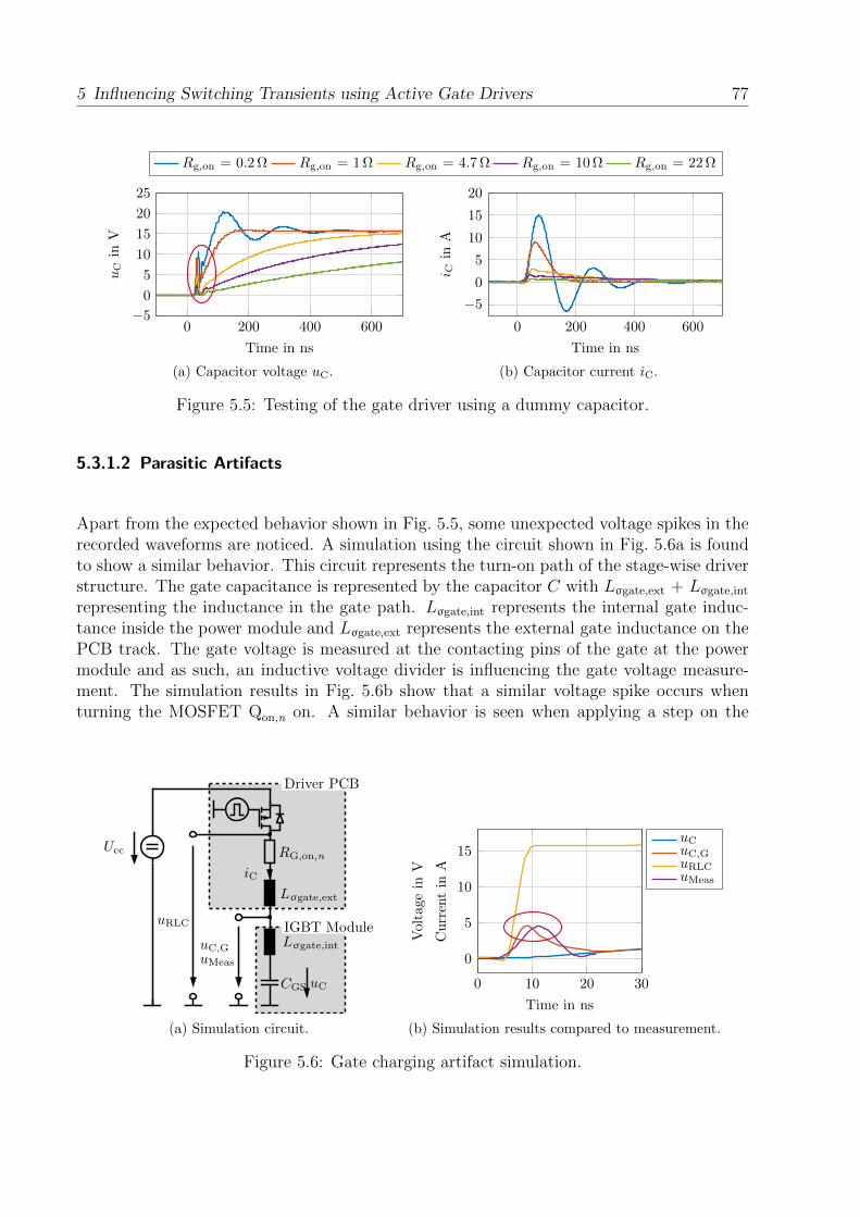
5 Influencing Switching Transients using Active Gate Drivers 77
Rg,on = 0.2 Ω Rg,on = 1 Ω Rg,on = 4.7 Ω Rg,on = 10 Ω Rg,on = 22 Ω
0 200 400 600−5
0
5
10
15
20
25
Time in ns
uCin
V
(a) Capacitor voltage uC.
0 200 400 600
−5
0
5
10
15
20
Time in ns
i Cin
A
(b) Capacitor current iC.
Figure 5.5: Testing of the gate driver using a dummy capacitor.
5.3.1.2 Parasitic Artifacts
Apart from the expected behavior shown in Fig. 5.5, some unexpected voltage spikes in therecorded waveforms are noticed. A simulation using the circuit shown in Fig. 5.6a is foundto show a similar behavior. This circuit represents the turn-on path of the stage-wise driverstructure. The gate capacitance is represented by the capacitor C with Lσgate,ext + Lσgate,int
representing the inductance in the gate path. Lσgate,int represents the internal gate induc-tance inside the power module and Lσgate,ext represents the external gate inductance on thePCB track. The gate voltage is measured at the contacting pins of the gate at the powermodule and as such, an inductive voltage divider is influencing the gate voltage measure-ment. The simulation results in Fig. 5.6b show that a similar voltage spike occurs whenturning the MOSFET Qon,n on. A similar behavior is seen when applying a step on the
uC,G
uC
uRLC
RG,on,nUcc
Driver PCB
IGBT Module
Lσgate,ext
Lσgate,int
iC
CGS
uMeas
(a) Simulation circuit.
0 10 20 30
0
5
10
15
Time in ns
Voltage
inV
Currentin
A
uCuC,GuRLCuMeas
(b) Simulation results compared to measurement.
Figure 5.6: Gate charging artifact simulation.
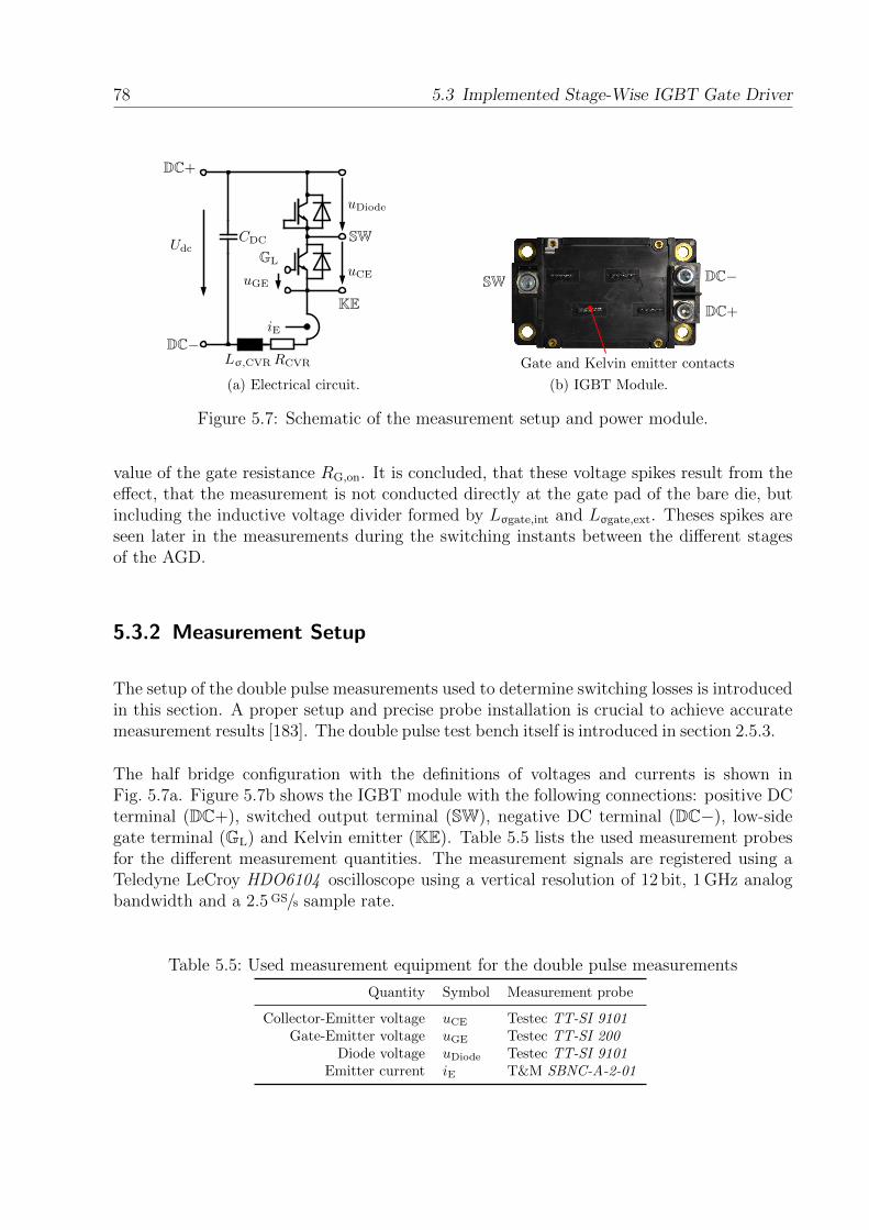
78 5.3 Implemented Stage-Wise IGBT Gate Driver
uGE
KE
uCE
iE
uDiode
DC+
DC−
CDC SWGL
Udc
RCVRLσ,CVR
(a) Electrical circuit.
SW
DC+
DC−
Gate and Kelvin emitter contacts
(b) IGBT Module.
Figure 5.7: Schematic of the measurement setup and power module.
value of the gate resistance RG,on. It is concluded, that these voltage spikes result from theeffect, that the measurement is not conducted directly at the gate pad of the bare die, butincluding the inductive voltage divider formed by Lσgate,int and Lσgate,ext. Theses spikes areseen later in the measurements during the switching instants between the different stagesof the AGD.
5.3.2 Measurement Setup
The setup of the double pulse measurements used to determine switching losses is introducedin this section. A proper setup and precise probe installation is crucial to achieve accuratemeasurement results [183]. The double pulse test bench itself is introduced in section 2.5.3.
The half bridge configuration with the definitions of voltages and currents is shown inFig. 5.7a. Figure 5.7b shows the IGBT module with the following connections: positive DCterminal (DC+), switched output terminal (SW), negative DC terminal (DC−), low-sidegate terminal (GL) and Kelvin emitter (KE). Table 5.5 lists the used measurement probesfor the different measurement quantities. The measurement signals are registered using aTeledyne LeCroy HDO6104 oscilloscope using a vertical resolution of 12 bit, 1 GHz analogbandwidth and a 2.5 GS/s sample rate.
Table 5.5: Used measurement equipment for the double pulse measurements
Quantity Symbol Measurement probe
Collector-Emitter voltage uCE Testec TT-SI 9101Gate-Emitter voltage uGE Testec TT-SI 200
Diode voltage uDiode Testec TT-SI 9101Emitter current iE T&M SBNC-A-2-01
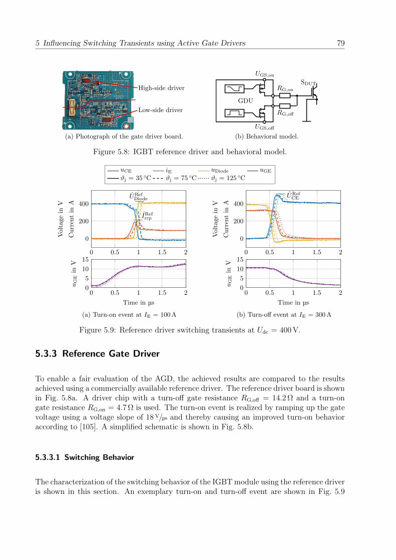
5 Influencing Switching Transients using Active Gate Drivers 79
High-side driver
Low-side driver
(a) Photograph of the gate driver board.
GDU
RG,on
RG,off
UGS,on
UGS,off
SDUT
(b) Behavioral model.
Figure 5.8: IGBT reference driver and behavioral model.
uCE iE uDiode uGE
ϑj = 35 C ϑj = 75 C ϑj = 125 C
0 0.5 1 1.5 2
0
200
400
Voltage
inV
Currentin
A
IRefrrp
URefDiode
0 0.5 1 1.5 20
5
10
15
Time in µs
uGEin
V
(a) Turn-on event at IE = 100 A
0 0.5 1 1.5 2
0
200
400
Voltage
inV
Currentin
A
URefCE
0 0.5 1 1.5 20
5
10
15
Time in µs
uGEin
V
(b) Turn-off event at IE = 300 A
Figure 5.9: Reference driver switching transients at Udc = 400 V.
5.3.3 Reference Gate Driver
To enable a fair evaluation of the AGD, the achieved results are compared to the resultsachieved using a commercially available reference driver. The reference driver board is shownin Fig. 5.8a. A driver chip with a turn-off gate resistance RG,off = 14.2 Ω and a turn-ongate resistance RG,on = 4.7 Ω is used. The turn-on event is realized by ramping up the gatevoltage using a voltage slope of 18 V/µs and thereby causing an improved turn-on behavioraccording to [105]. A simplified schematic is shown in Fig. 5.8b.
5.3.3.1 Switching Behavior
The characterization of the switching behavior of the IGBT module using the reference driveris shown in this section. An exemplary turn-on and turn-off event are shown in Fig. 5.9

80 5.3 Implemented Stage-Wise IGBT Gate Driver
Udc = 200V Udc = 400V ϑj = 35 C ϑj = 75 C ϑj = 125 C
0 100 200 3000
10
20
30
40
Current iE in A
Eon,Switch
inmJ
(a) Switch turn-on losses.
0 100 200 3000
1
2
Current iE in A
Eoff,D
iodein
mJ
(b) Diode turn-off losses duringthe switch turn-on event.(i)
0 100 200 3000
10
20
30
Current iE in A
Eoffin
mJ
(c) Switch turn-off losses. [81]
Figure 5.10: Reference driver switching losses using.
at a dc-link voltage Udc = 400 V and a load current IE = 300 A for the three junctiontemperatures ϑj = 35 C, 75 C and 125 C. The gate voltage uGE, the collector-emittervoltage uCE, the emitter current iE and the high-side diode voltage uDiode are plotted. Thecharacteristic reverse recovery current IRef
rrp and maximum diode voltage URefDiode is seen in
Fig. 5.9a together with the peak collector-emitter voltage URefCE in Fig. 5.9b.
Switching Losses
The switching losses of the IGBT device are measured at the nominal operating pointsshown in Table 5.2. The resulting switching losses are shown in Fig. 5.10. The turn-offlosses Eoff are shown in Fig. 5.10c whereas the turn-on losses Eon are split into the deviceturn-on losses Eon,Switch (see Fig. 5.10a) and the diode turn-off losses Eoff,Diode (Fig. 5.10b).It is noticed, that the diode losses Eoff,Diode are by an order of magnitude smaller comparedto the switch losses Eon,Switch.
Device Stress
The occurring device stress using the reference driver is shown in Fig. 5.11 for the threejunction temperatures ϑj = 35 C, 75 C and 125 C. A saturation of the peak reverse
recovery current ∆Irrp is observed for an emitter current IE > 200 A while a linear relation
is observed between the peak collector-emitter voltage ∆UCE and the emitter current IE.
(i)The step in the Udc = 400 V, ϑj = 35 C waveform is due to ringing in the power loss waveforms, whichforces the integration border detection to jitter.

5 Influencing Switching Transients using Active Gate Drivers 81
Udc = 200V Udc = 400V ϑj = 35 C ϑj = 75 C ϑj = 125 C
0 100 200 3000
50
100
150
Current IE in A
∆I r
rpin
A
(a) Reverse recovery peakcurrent ∆Irrp.
0 100 200 3000
50
100
150
Current IE in A
∆UCE
inV
(b) Switch voltage overshoot∆UCE.
0 100 200 3000
20
40
Current IE in A
∆UDiode
inV
(c) Diode voltage overshoot∆UDiode.(ii)
Figure 5.11: Device stress using the reference driver.
The voltage stress on the diode is highest for partial loads, as it is seen in Fig. 5.11c, wherethe peak stress occurs at an emitter current IE = 100 A.
5.3.4 Active Gate Driver Operation
The influence of the stage-wise driver on the switching behavior is evaluated using an ex-perimental approach. The resulting switching transients are compared to each other usingdifferent configurations of the driver according to the gate driving strategy as described insection 5.2.3. The investigation is split into four sections. The turn-off behavior and theturn-on behavior are analyzed individually. For each switching event, a detailed analysisusing a two and a three-stage operation is conducted.
5.3.4.1 Single-Stage Turn-Off Event Behavior
The single stage operation is equivalent to the reference operation, which is presented insection 5.3.3 except for a different gate resistor. A higher gate resistor slows down theswitching event and hence, reduces the stress on the device. At the same time, the switchinglosses Esw are increased.
(ii)Due to different scaling of the measurement probe and scaling of the oscilloscope input, a higher noiselevel is seen for the Udc = 400 V measurements.

82 5.3 Implemented Stage-Wise IGBT Gate Driver
200 400 6000
200
400
iE
uCE
Time in ns
Cu
rren
tin
A
Volt
age
inV
RS2g,off = 33 Ω
RS2g,off = 56 Ω
RS2g,off = 100 Ω
Figure 5.12: Turn-off event using different gate resistors at Udc = 400 V, IE = 300 A,ϑj = 35 C. [81]
5.3.4.2 Two-Stage Turn-Off Event Behavior
The two-stage operation of the driver handles about a second stage, which is introducedafter a certain time ∆tS1
off . At first the influence of the second stage resistor value RS2G,off is
shown in Fig. 5.12. A series of turn-off events are plotted for a dc-link voltage of Udc = 400 V,a load current IE = 300 A and a junction temperature ϑj = 35 C. The duration of the firststage is chosen to ∆tS1
off = 400 ns using a gate resistor RS1G,off = 4.7 Ω. The second stage gate
resistor is varied from RS2G,off = 33 Ω to 100 Ω. From the resulting waveforms, it is seen that
the collector-emitter peak voltage UCE is slightly reduced with a higher resistor value. Aslower decaying of the emitter current iE is seen, which leads to higher turn-off losses.
Second, the influence of the duration ∆tS1off of the first stage is investigated. The driver is
configured using the setup listed in Table 5.6. The variation of the time ∆tS1off is conducted
using a 10 ns step size. The resulting waveforms are plotted in Fig. 5.13a together withthe corresponding losses in Fig. 5.13b. A higher duration ∆tS1
off results in a higher voltageovershoot and faster decaying of the emitter current iE. Accordingly, the switching lossesare rising with a shorter first stage as the discharging of the gate capacitance is sloweddown. The observed behavior is already shown in [81], [106]. The voltage spikes, which areobserved in the gate voltage uGE, are explained by the artifact presented in section 5.3.1.2.The presented behavioral influence is valid for any other dc-link voltage, load current andtemperature. Thus, a direct link between the voltage overshoot UCE and the first stagetiming ∆tS1
off is deduced.
The variation of the individual resistance of the various stages is not further considered
Table 5.6: Turn-off driver configuration [81]
Stage S RSnG,off ∆tSnoff
S1 RG,off,1 = 4.7 Ω 410 ns . . . 440 nsS2 RG,off,3 = 33 Ω ∞
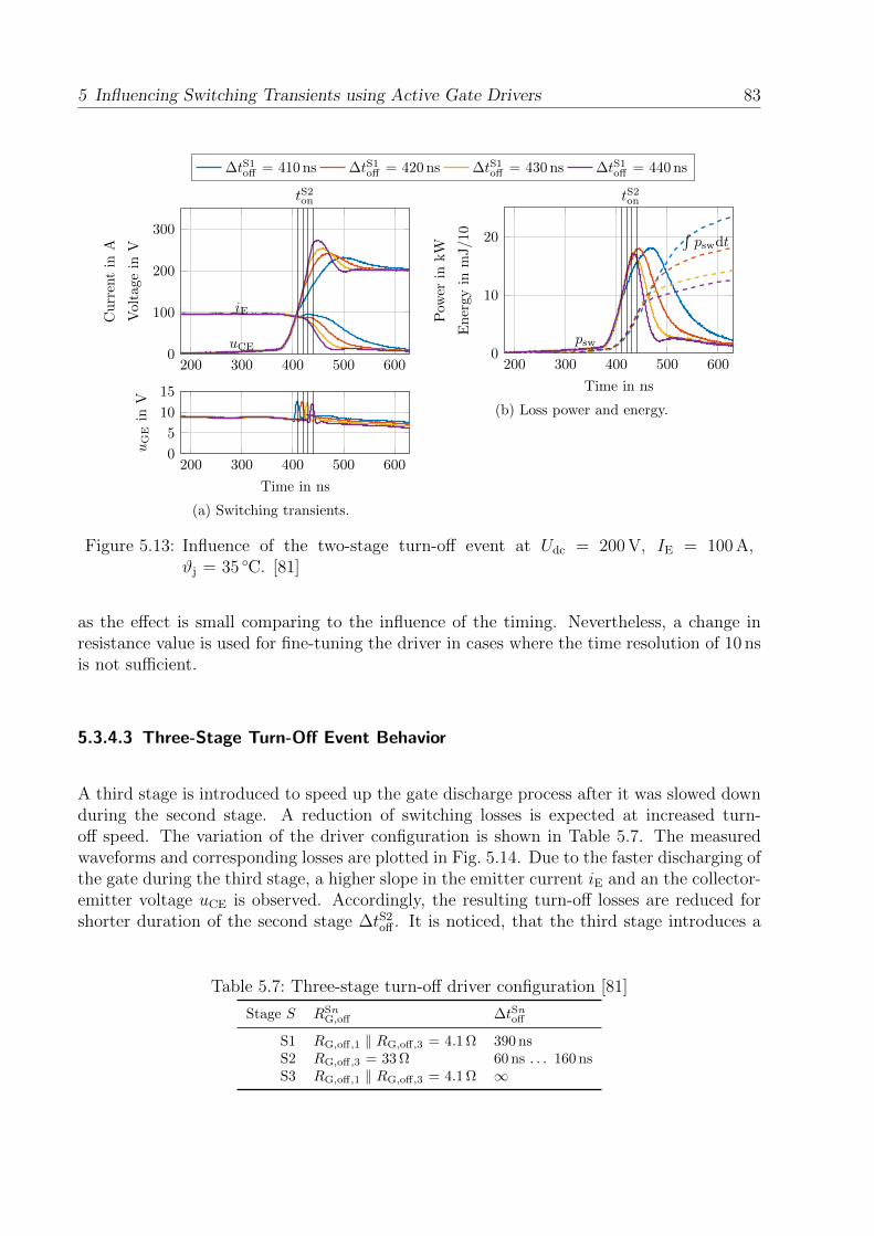
5 Influencing Switching Transients using Active Gate Drivers 83
∆tS1off = 410 ns ∆tS1
off = 420 ns ∆tS1off = 430 ns ∆tS1
off = 440 ns
200 300 400 500 6000
100
200
300
iE
uCE
Currentin
A
Voltagein
V
tS2on
200 300 400 500 6000
5
10
15
Time in ns
uGEin
V
(a) Switching transients.
200 300 400 500 6000
10
20
psw
´
pswdt
Time in ns
Pow
erin
kW
Energy
inmJ/10
tS2on
(b) Loss power and energy.
Figure 5.13: Influence of the two-stage turn-off event at Udc = 200 V, IE = 100 A,ϑj = 35 C. [81]
as the effect is small comparing to the influence of the timing. Nevertheless, a change inresistance value is used for fine-tuning the driver in cases where the time resolution of 10 nsis not sufficient.
5.3.4.3 Three-Stage Turn-Off Event Behavior
A third stage is introduced to speed up the gate discharge process after it was slowed downduring the second stage. A reduction of switching losses is expected at increased turn-off speed. The variation of the driver configuration is shown in Table 5.7. The measuredwaveforms and corresponding losses are plotted in Fig. 5.14. Due to the faster discharging ofthe gate during the third stage, a higher slope in the emitter current iE and an the collector-emitter voltage uCE is observed. Accordingly, the resulting turn-off losses are reduced forshorter duration of the second stage ∆tS2
off . It is noticed, that the third stage introduces a
Table 5.7: Three-stage turn-off driver configuration [81]
Stage S RSnG,off ∆tSnoff
S1 RG,off,1 ‖ RG,off,3 = 4.1 Ω 390 nsS2 RG,off,3 = 33 Ω 60 ns . . . 160 nsS3 RG,off,1 ‖ RG,off,3 = 4.1 Ω ∞

84 5.3 Implemented Stage-Wise IGBT Gate Driver
∆tS2off = 60 ns ∆tS2
off = 80 ns ∆tS2off = 100 ns
∆tS2off = 120 ns ∆tS2
off = 140 ns ∆tS2off = 160 ns
100 200 300 400 500 6000
100
200
300
iEuCE
Currentin
A
Voltagein
V
tS2on tS3
on
100 200 300 400 500 6000
5
10
15
Time in ns
uGEin
V
(a) Switch waveforms.
100 200 300 400 500 6000
20
40
psw´
pswdt
Time in ns
Pow
erin
kW
Energy
inmJ/10
tS2on tS3
on
(b) Switching losses.
Figure 5.14: Various three-stage turn-off events at Udc = 200 V, IE = 200 A andϑj = 125 C. [81]
second bump in the collector-emitter voltage uCE which might violate the maximum peakvoltage stress as seen for example using ∆tS2
off = 60 ns. A long duration of the second stage(e.g., ∆tS2
off = 160 ns) is equivalent to a two stage operation and is thus used here to evaluatethe achievements of the third stage. In fact, adding a third stage results in reduced turn-offlosses compared to the two stage operation.
The following section presents the influence of the stage-wise gate driver on the turn-onbehavior of the IGBT. Analogously to the turn-off investigation, the turn-on behavior in-vestigation is split in a two- and three-stage operation.
5.3.4.4 Single-Stage Turn-On Event Behavior
The single stage operation is equivalent to the operation using a standard gate driver asdescribed in section 2.2. A high gate resistance slows down the turn-on event, thus reducesthe current overshoot and increases the turn-on losses.
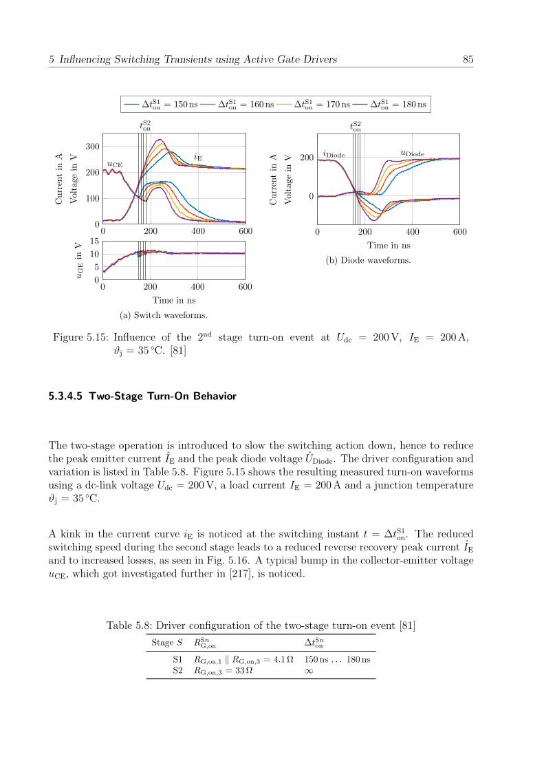
5 Influencing Switching Transients using Active Gate Drivers 85
∆tS1on = 150 ns ∆tS1on = 160 ns ∆tS1on = 170 ns ∆tS1on = 180 ns
0 200 400 6000
100
200
300iE
uCE
Currentin
A
Voltage
inV
tS2on
0 200 400 6000
5
10
15
Time in ns
uGEin
V
(a) Switch waveforms.
0 200 400 600
0
200uDiodeiDiode
Time in ns
Currentin
A
Voltage
inV
tS2on
(b) Diode waveforms.
Figure 5.15: Influence of the 2nd stage turn-on event at Udc = 200 V, IE = 200 A,ϑj = 35 C. [81]
5.3.4.5 Two-Stage Turn-On Behavior
The two-stage operation is introduced to slow the switching action down, hence to reducethe peak emitter current IE and the peak diode voltage UDiode. The driver configuration andvariation is listed in Table 5.8. Figure 5.15 shows the resulting measured turn-on waveformsusing a dc-link voltage Udc = 200 V, a load current IE = 200 A and a junction temperatureϑj = 35 C.
A kink in the current curve iE is noticed at the switching instant t = ∆tS1on. The reduced
switching speed during the second stage leads to a reduced reverse recovery peak current IE
and to increased losses, as seen in Fig. 5.16. A typical bump in the collector-emitter voltageuCE, which got investigated further in [217], is noticed.
Table 5.8: Driver configuration of the two-stage turn-on event [81]
Stage S RSnG,on ∆tSnon
S1 RG,on,1 ‖ RG,on,3 = 4.1 Ω 150 ns . . . 180 nsS2 RG,on,3 = 33 Ω ∞
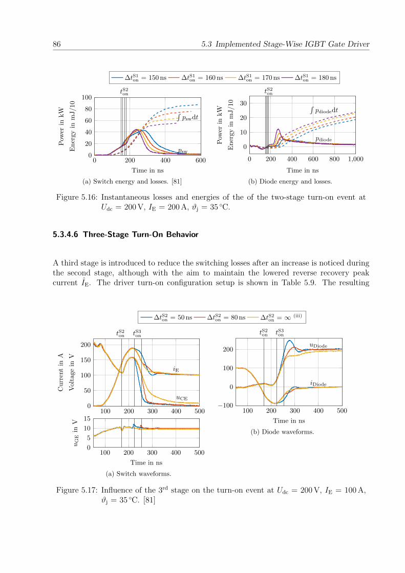
86 5.3 Implemented Stage-Wise IGBT Gate Driver
∆tS1on = 150 ns ∆tS1on = 160 ns ∆tS1on = 170 ns ∆tS1on = 180 ns
0 200 400 6000
20
40
60
80
100
psw
´
pswdt
Time in ns
Pow
erin
kW
Energy
inmJ/10
tS2on
(a) Switch energy and losses. [81]
0 200 400 600 800 1,000
0
10
20
30
pdiode
´
pdiodedt
Time in ns
Pow
erin
kW
Energy
inmJ/10
tS2on
(b) Diode energy and losses.
Figure 5.16: Instantaneous losses and energies of the of the two-stage turn-on event atUdc = 200 V, IE = 200 A, ϑj = 35 C.
5.3.4.6 Three-Stage Turn-On Behavior
A third stage is introduced to reduce the switching losses after an increase is noticed duringthe second stage, although with the aim to maintain the lowered reverse recovery peakcurrent IE. The driver turn-on configuration setup is shown in Table 5.9. The resulting
∆tS2on = 50 ns ∆tS2on = 80 ns ∆tS2on = ∞ (iii)
100 200 300 400 5000
50
100
150
200
iE
uCE
Currentin
A
Voltage
inV
tS2on tS3
on
100 200 300 400 5000
5
10
15
Time in ns
uGEin
V
(a) Switch waveforms.
100 200 300 400 500−100
0
100
200uDiode
iDiode
Time in ns
tS2on tS3
on
(b) Diode waveforms.
Figure 5.17: Influence of the 3rd stage on the turn-on event at Udc = 200 V, IE = 100 A,ϑj = 35 C. [81]
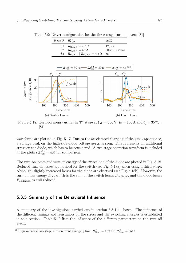
5 Influencing Switching Transients using Active Gate Drivers 87
Table 5.9: Driver configuration for the three-stage turn-on event [81]
Stage S RSnG,on ∆tSnon
S1 RG,on,1 = 4.7 Ω 170 nsS2 RG,on,4 = 56 Ω 50 ns . . . 80 nsS3 RG,on,1 ‖ RG,on,4 = 4.3 Ω ∞
∆tS2on = 50 ns ∆tS2on = 80 ns ∆tS2on = ∞ (iii)
100 200 300 400 5000
10
20
30
psw
´
pswdt
Time in ns
Pow
erin
kW
Energy
inmJ/10
tS2on tS3
on
(a) Switch losses.
100 200 300 400 500
0
5
10
pdiode
´
pdiodedt
Time in ns
tS2on tS3
on
(b) Diode losses.
Figure 5.18: Turn-on energy using the 3rd stage at Udc = 200 V, IE = 100 A and ϑj = 35 C.[81]
waveforms are plotted in Fig. 5.17. Due to the accelerated charging of the gate capacitance,a voltage peak on the high-side diode voltage uDiode is seen. This represents an additionalstress on the diode, which has to be considered. A two-stage operation waveform is includedin the plots (∆tS2
on = ∞) for comparison.
The turn-on losses and turn-on energy of the switch and of the diode are plotted in Fig. 5.18.Reduced turn-on losses are noticed for the switch (see Fig. 5.18a) when using a third stage.Although, slightly increased losses for the diode are observed (see Fig. 5.18b). However, theturn-on loss energy Eon, which is the sum of the switch losses Eon,Switch and the diode lossesEoff,Diode, is still reduced.
5.3.5 Summary of the Behavioral Influence
A summary of the investigations carried out in section 5.3.4 is shown. The influence ofthe different timings and resistances on the stress and the switching energies is establishedin this section. Table 5.10 lists the influence of the different parameters on the turn-offevent.
(iii)Equivalents a two-stage turn-on event changing from RS1G,on = 4.7 Ω to RS2
G,on = 65 Ω.

88 5.3 Implemented Stage-Wise IGBT Gate Driver
Table 5.10: Summary of the turn-off behavior
UCE Eoff Reference
RS1G,off↑ —
∆tS1off ↑ Fig. 5.13
RS2G,off↑ Fig. 5.12
∆tS2off ↑ Fig. 5.14
RS3G,off↑ —
Table 5.11: Summary of the turn-on behavior
Irrp UDiode Eon,Switch Eoff,Diode Eon Reference
RS1G,on↑ (iv) —
∆tS1on ↑ Fig. 5.15, Fig. 5.16
RS2G,on↑ — (iv) —
∆tS2on ↑ — Fig. 5.17, Fig. 5.18
RS3G,on↑ — (iv) —
Analogously, Table 5.11 shows the influence of the resistor and timing settings during the dif-ferent stages on the device stress (Irrp, UDiode) and the switching energy (Eon,Switch, Eoff,Diode)of the turn-on event.
5.3.6 Optimization Procedure
Previously, the impact of the different stages on the switching behavior was shown. Thissection shows the developed optimization algorithm, which is extracted from Table 5.10 andTable 5.11. In this section, optimized behavior is defined as equal device stress as comparedto the reference driver, however with reduced switching losses. The current and voltageslopes are not considered including any impact thereof on the EMI.
5.3.6.1 Turn-Off Optimization
The turn-off optimization procedure is split into two stages. At first, the optimum operationfor a two-stage operation has to be found. This optimization guarantees, that the powersemiconductor switches off as fast as possible while producing the same voltage overshootUCE as the reference driver. The second operation step is conducted to find the optimizedsettings of the third stage of the stage-wise driver. The third stage allows further reduction of
(iv)The effect of the resistance on the diode losses did not get investigated.
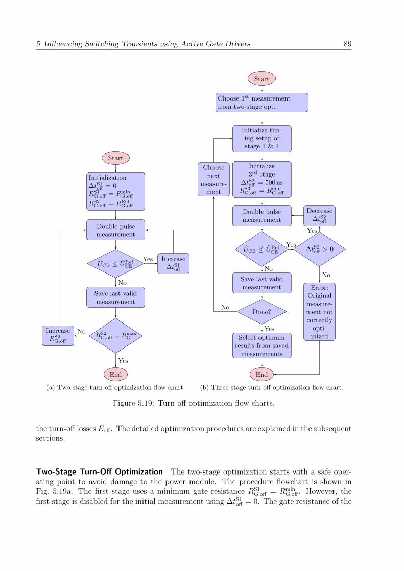
5 Influencing Switching Transients using Active Gate Drivers 89
Start
Initialization∆tS1
off = 0RS1
G,off = RminG,off
RS2G,off = RRef
G,off
Double pulsemeasurement
UCE ≤ URefCE
Increase∆tS1
off
Save last validmeasurement
RS2G,off =Rmax
G
IncreaseRS2
G,off
End
Yes
No
No
Yes
(a) Two-stage turn-off optimization flow chart.
Start
Choose 1st measurementfrom two-stage opt.
Initialize tim-ing setup ofstage 1 & 2
Initialize3rd stage
∆tS2off = 500 ns
RS3G,off = Rmin
G,off
Double pulsemeasurement
UCE ≤ URefCE ∆tS2
off > 0
Decrease∆tS2
off
Error:Originalmeasure-ment notcorrectly
opti-mized
Save last validmeasurement
Done?
Choosenext
measure-ment
Select optimumresults from saved
measurements
End
Yes
Yes
NoNo
Yes
No
(b) Three-stage turn-off optimization flow chart.
Figure 5.19: Turn-off optimization flow charts.
the turn-off losses Eoff . The detailed optimization procedures are explained in the subsequentsections.
Two-Stage Turn-Off Optimization The two-stage optimization starts with a safe oper-ating point to avoid damage to the power module. The procedure flowchart is shown inFig. 5.19a. The first stage uses a minimum gate resistance RS1
G,off = RminG,off . However, the
first stage is disabled for the initial measurement using ∆tS1off = 0. The gate resistance of the

90 5.3 Implemented Stage-Wise IGBT Gate Driver
reference driver is used for the second stage RS2G,off = RG,off . This guarantees no violation of
the maximum voltage overshoot UCE ≤ URefCE .
In the next step, the active time of the first stage ∆tS1off is increased until the overvoltage
constraint is violated. As the overvoltage UCE is observed and is only increased in smallsteps, the power device does not get harmed. An increase of the second stage resistorRS2
G,off decreases the voltage peak UCE as it slows down the switching action. Using a fewiterations, the first-stage time ∆tS1
off can be increased further to achieve reduced turn-offlosses. All valid measurements have to be saved as they are potential candidates for thethird stage optimization.
Three-Stage Turn-Off Optimization The third stage is used to speed up the final switch-ing event after peak stress on the device is reduced. The procedure flowchart is shown inFig. 5.19b. As an initial setup, the minimum gate resistance is used for the last stageRS3
G,off = RminG,off . The initial time ∆tS2
off is chosen large enough to have no influence on theswitching event at first (∆tS2
off = 500 ns). Every resulting measurement from the two-stageoptimization is subject to an three-stage optimization. In the end, the best result is se-lected.
By reducing the time of the third stage timing ∆tS2off , a second peak is appearing in the
collector-emitter voltage uCE as it is seen in Fig. 5.14b. The time ∆tS2off is reduced until
this secondary peak voltage violates the constraint. If the time ∆tS2off reaches zero before
the voltage constraint is reached, then a wrong initial measurement, which has not beenproperly optimized, has been chosen. In this case, a further optimization is not possible andhence, an error is thrown. For the normal operation, the last valid measurement is savedand the next available measurement from the two-stage operation is selected. As seen insection 5.3.4.1, the resistor value has an additional minor influence on the stress and losses.Thus, the third stage gate resistance value RS3
G,off is used for minor adjustments where theFPGA time resolution is insufficient.
5.3.6.2 Turn-On Optimization
The turn-on optimization is carried out analogously to the turn-off optimization procedure,except, that in this case, the reverse recovery peak current Irrp and the high-side diode peak
voltage UDiode are considered.
Two-Stage Turn-On Optimization The turn-on optimization is initialized with a highgate resistance to guarantee a safe operating point as shown in the flowchart in Fig. 5.20a.The reference driver setup cannot be chosen here as it uses an advanced turn-on procedure(see section 5.3.3), which gives improved switching behavior compared to a standard push

5 Influencing Switching Transients using Active Gate Drivers 91
Start
Initialization∆tS1
on = 0RS1
G,on = RminG,on
RS2G,on = RG,on,equiv
Double pulsemeasurement
UDiode ≤ URefDiode
Irrp ≤ IRefrrp
Increase∆tS1
on
Save last validmeasurement
RS2G,on =Rmax
G
IncreaseRS2
G,on
End
Yes
No
No
Yes
(a) Two-stage turn-on optimization flowchart.
Start
Choose 1st valid measure-ment from two-stage opt.
Initialize tim-ing setup ofstage 1 & 2
Initializethird stage
∆tS2on = 500 ns
RS3G,on = Rmin
G,on
Double pulsemeasurement
UCE ≤ URefCE
UDiode ≤ URefDiode
Irrp ≤ IRefrrp
Decrease∆tS2
on
Error:Originalmeasure-ment notcorrectly
opti-mized
Save last validmeasurement
Done?
Choosenext
measure-ment
Select optimumresults from saved
measurements
End
Yes
Yes
No
No
Yes
No
(b) Three-stage turn-on optimization flow chart.
Figure 5.20: Turn-on optimization flow charts.
stage using the given turn-on gate resistor RG,on. An equivalent turn-on resistance RG,on,equiv
has to be found experimentally which results in an less or equal reverse recovery peak currentIrrp and less or equal diode peak-voltage UDiode compared to the reference driver. This isachieved by starting with a high gate resistor (e.g. RS2
G,on = 100 Ω) and reducing it until thestress on the device exceeds the reference values. The resulting equivalent gate resistanceRG,on,equiv is chosen as initial setup RS2
G,on = RG,on,equiv for the optimization strategy. Thefirst stage, which is using the minimum gate resistance RS1
G,on = RminG,on, is initially disabled by

92 5.3 Implemented Stage-Wise IGBT Gate Driver
using a time ∆tS1on = 0. The turn-on optimization is carried out by increasing the first-stage
time ∆tS1on step by step and observing, whether the constraints get violated or not. In case of
a violation, the second stage resistor RS2G,on is increased to further slow down the switching
during the second stage and hence reduce the overcurrent Irrp and the overvoltage UDiode.
Three-Stage Turn-On Optimization Analogously to the three-stage turn-off optimiza-tion, the flowchart of the three-stage turn-on optimization is plotted in Fig. 5.20b. The goalof the third stage is to increase the switching speed after the peak stress on the switch andthe diode happened to further reduce the switching losses. Therefore, a small resistance ischosen to allow a high gate current. The optimization is initialized using a large time ∆tS2
on
(e.g. 500 ns), such that the third stage does not have any influence on the switching behaviorat first. This time is then successively reduced. If the time ∆tS2
on reaches zero before theconstraints are violated, then a wrong initial measurement, which has not been properlyoptimized, has been chosen. A further optimization is not possible and hence, an error isthrown.
5.3.7 Application of the Proposed Optimization Algorithm
The switching losses and the peak voltages and currents are extracted from the result-ing measurements. The extracted switching losses are plotted against the device stress inFig. 5.21 for an exemplary operating point Udc = 400 V, IE = 200 A and ϑj = 35 C. Allthe conducted measurements, which have been made during the optimization procedure,are included in the graph. The axis are per unit (p.u.), normalized to the correspondingreference driver values and defined as follows:
eoff =Eoff
ERefoff
eon =Eon
ERefon
irrp =Irrp
IRefrrp
uCE =UCE
URefCE
uDiode =UDiode
URefDiode
Different colored dots represent different resistor sets whereas same color points representmeasurements with the same resistor set, but with different timing settings. A Pareto front isrecognized, which proves that the optimization algorithm reaches the optimum configurationand no further improvement is possible.
The optimization algorithm is applied to the before mentioned operating points listed inTable 5.2. In total, 18 optimizations (resulting from 2 dc-link voltages, 3 temperatures and3 current levels according to Table 5.2) are carried out for the turn-on and turn-off events,resulting in a total of 36 measurement series. The results are plotted in section A.3.4. Itis seen that, depending on the configuration of the stage-wise driver, the voltage overshoot
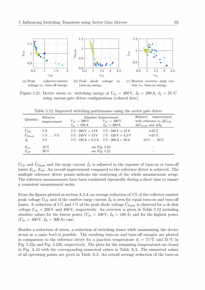
5 Influencing Switching Transients using Active Gate Drivers 93
0.5 1 1.5 2
0.9
1
1.1
eoff
uC
E
(a) Peak collector-emittervoltage vs. turn-off energy.
0.5 1 1.5 2 2.50.8
0.9
1
1.1
eonuDiode
(b) Peak diode voltage vs.turn-on energy.
0.5 1 1.5 2 2.5
0.8
1
1.2
eon
i rrp
(c) Reverse recovery peak cur-rent vs. turn-on energy.
Figure 5.21: Device stress vs. switching energy at Udc = 400 V, IE = 200 A, ϑj = 35 Cusing various gate driver configurations (colored dots).
Table 5.12: Improved switching performance using the active gate driver
QuantityRelativeimprovement
Absolute Improvement Relative improvementwith reference to ∆UCE,∆UDiode and ∆IE
Udc = 200 VIdc = 100 A
Udc = 400 VIdc = 300 A
UCE 5 % 5 % · 260 V = 13 V 5 % · 500 V = 25 V ≈23 %
UDiode 1 % . . . 5 % 5 % · 240 V = 12 V 1 % · 420 V = 4.2 V ≈25 %
IE 5 % 5 % · 190 A = 9.5 A 5 % · 400 A = 20 A 10 % . . . 20 %
Eon 10 % see Fig. 5.22 —Eoff 30 % see Fig. 5.22 —
UCE and UDiode and the surge current IE is adjusted in the expense of turn-on or turn-offlosses Eon, Eoff . An overall improvement compared to the reference driver is achieved. Themultiple reference driver points indicate the scattering of the whole measurement setup.The reference measurements have been conducted repeatedly during a short time to ensurea consistent measurement series.
From the figures plotted in section A.3.4, an average reduction of 5 % of the collector-emitterpeak voltage UCE and of the emitter surge current IE is seen for equal turn-on and turn-offlosses. A reduction of 5 % and 1 % of the peak diode voltage UDiode is observed for a dc-linkvoltage Udc = 200 V and 400 V, respectively. An overview is given in Table 5.12 includingabsolute values for the lowest power (Udc = 100 V, IE = 100 A) and for the highest power(Udc = 400 V, IE = 300 A) case.
Besides a reduction of stress, a reduction of switching losses while maintaining the devicestress at a same level is possible. The resulting turn-on and turn-off energies are plottedin comparison to the reference driver for a junction temperature ϑj = 75 C and 35 C inFig. 5.22a and Fig. 5.22b, respectively. The plots for the remaining temperatures are foundin Fig. A.44 with the corresponding numerical values in Table A.3. The numerical valuesof all operating points are given in Table A.3. An overall average reduction of the turn-on
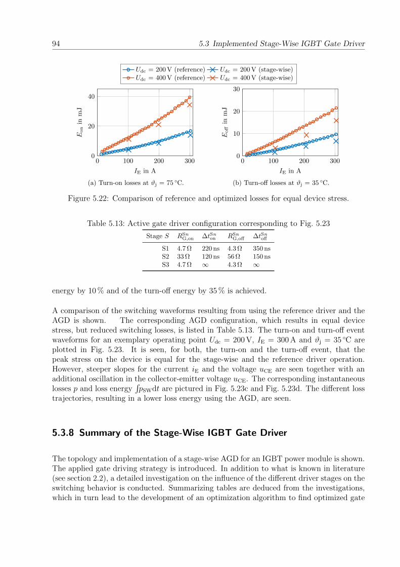
94 5.3 Implemented Stage-Wise IGBT Gate Driver
Udc = 200V (reference) Udc = 200V (stage-wise)Udc = 400V (reference) Udc = 400V (stage-wise)
0 100 200 3000
20
40
IE in A
Eonin
mJ
(a) Turn-on losses at ϑj = 75 C.
0 100 200 3000
10
20
30
IE in A
Eoffin
mJ
(b) Turn-off losses at ϑj = 35 C.
Figure 5.22: Comparison of reference and optimized losses for equal device stress.
Table 5.13: Active gate driver configuration corresponding to Fig. 5.23
Stage S RSnG,on ∆tSnon RSn
G,off ∆tSnoff
S1 4.7 Ω 220 ns 4.3 Ω 350 nsS2 33 Ω 120 ns 56 Ω 150 nsS3 4.7 Ω ∞ 4.3 Ω ∞
energy by 10 % and of the turn-off energy by 35 % is achieved.
A comparison of the switching waveforms resulting from using the reference driver and theAGD is shown. The corresponding AGD configuration, which results in equal devicestress, but reduced switching losses, is listed in Table 5.13. The turn-on and turn-off eventwaveforms for an exemplary operating point Udc = 200 V, IE = 300 A and ϑj = 35 C areplotted in Fig. 5.23. It is seen, for both, the turn-on and the turn-off event, that thepeak stress on the device is equal for the stage-wise and the reference driver operation.However, steeper slopes for the current iE and the voltage uCE are seen together with anadditional oscillation in the collector-emitter voltage uCE. The corresponding instantaneouslosses p and loss energy
´
pSWdt are pictured in Fig. 5.23c and Fig. 5.23d. The different losstrajectories, resulting in a lower loss energy using the AGD, are seen.
5.3.8 Summary of the Stage-Wise IGBT Gate Driver
The topology and implementation of a stage-wise AGD for an IGBT power module is shown.The applied gate driving strategy is introduced. In addition to what is known in literature(see section 2.2), a detailed investigation on the influence of the different driver stages on theswitching behavior is conducted. Summarizing tables are deduced from the investigations,which in turn lead to the development of an optimization algorithm to find optimized gate
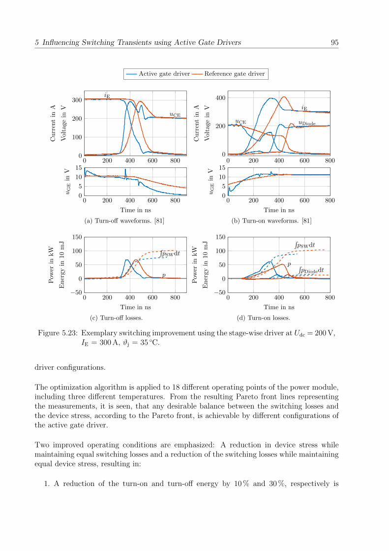
5 Influencing Switching Transients using Active Gate Drivers 95
iE uCE
Active gate driver Reference gate driver
0 200 400 600 8000
100
200
300iE
uCE
Currentin
A
Voltage
inV
0 200 400 600 8000
5
10
15
Time in ns
uGEin
V
(a) Turn-off waveforms. [81]
0 200 400 600 800−50
0
50
100
150
p
´
pSWdt
Time in ns
Pow
erin
kW
Energy
in10
mJ
(c) Turn-off losses.
0 200 400 600 8000
200
400
iE
uCE uDiode
Currentin
A
Voltagein
V0 200 400 600 800
0
5
10
15
Time in nsuGEin
V
(b) Turn-on waveforms. [81]
0 200 400 600 800−50
0
50
100
150
p
´
pSWdt
´
pDiodedt
Time in ns
Pow
erin
kW
Energy
in10
mJ
(d) Turn-on losses.
Figure 5.23: Exemplary switching improvement using the stage-wise driver at Udc = 200 V,IE = 300 A, ϑj = 35 C.
driver configurations.
The optimization algorithm is applied to 18 different operating points of the power module,including three different temperatures. From the resulting Pareto front lines representingthe measurements, it is seen, that any desirable balance between the switching losses andthe device stress, according to the Pareto front, is achievable by different configurations ofthe active gate driver.
Two improved operating conditions are emphasized: A reduction in device stress whilemaintaining equal switching losses and a reduction of the switching losses while maintainingequal device stress, resulting in:
1. A reduction of the turn-on and turn-off energy by 10 % and 30 %, respectively is

96 5.4 Implemented Stage-Wise SiC MOSFET Gate Driver
achieved while maintaining an equal stress on the device.
2. A reduction of the voltage stress ∆UCE and ∆UDiode by ≈25 % and of the currentstress ∆IE by 10 % . . . 20 % is achieved for equal switching energies.
5.4 Implemented Stage-Wise SiC MOSFET Gate Driver
In this section, the implementation of the presented stage-wise gate driver topology is shownfor a WBG device: a Cree CPM2-1200-0040B 1200 V SiC MOSFET with an internal gateresistance RG,int = 1.8 Ω [218]. Compared to the IGBT gate driver, new challenges in termsof timing arise as the switching speed is by at least a decade faster [90]. In turn, thismeans that the time resolution of the logic signals has to be increased by at least a decade.In contrast to the preceding investigations on the AGD for IGBTs, only a single operatingpoint is subject to the investigation. A dc-link voltage Udc = 700 V, a nominal source currentIS = 60 A and a junction temperature ϑj = 35 C is used. The device specifications and thetest conditions are listed in Table 5.14.
5.4.1 Driver Hardware
The schematic of the gate driver including the parasitic elements of the PCB is pictured inFig. 5.24. The gate drive unit (GDU) is powered using a galvanic isolated power supply. Therelevant measured quantities are the low-side drain-source voltage uDS, the source currentiS and the high-side diode voltage uDiode.
5.4.1.1 Driver Board
The schematic of a single branch of the stage-wise gate driver is pictured in Fig. 5.25. Variousdifferent driver ICs (ICn) in combination with the n- and p-channel MOSFETs (Qon,n, Qoff,n)got investigated experimentally to find the combination, which allows the fastest charging
Table 5.14: Specifications of the SiC MOSFET and test setup [143]
Description Specifier Value
Blocking voltage UDSS 1200 VRated current IS 63 A
DC-link voltage Udc 700 VTest current IS 60 AJunction temperature ϑj 35 C
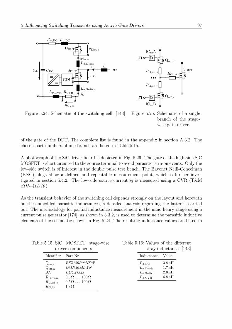
5 Influencing Switching Transients using Active Gate Drivers 97
GDU
HalbbruckeStepwise-Treiber
Verbindung
Shunt-Widerstand
Steuereinheit
iS
SDUT
DDUT
Lσ,DCRσ,DC
Udc CDC
uDiode
uDS
Lσ,Switch
Lσ,Diode
Lσ,CVR RCVR
uCVR
HV-Zwischenkreis
iDiode
iL L
=
=
Figure 5.24: Schematic of the switching cell. [143]
SDUT
Qon,n
Qoff,n
RG,on,n
RG,off,n
ICn,A
ICn,B
RG,int
Figure 5.25: Schematic of a singlebranch of the stage-wise gate driver.
of the gate of the DUT. The complete list is found in the appendix in section A.3.2. Thechosen part numbers of one branch are listed in Table 5.15.
A photograph of the SiC driver board is depicted in Fig. 5.26. The gate of the high-side SiCMOSFET is short circuited to the source terminal to avoid parasitic turn-on events. Only thelow-side switch is of interest in the double pulse test bench. The Bayonet Neill-Concelman(BNC) plugs allow a defined and repeatable measurement point, which is further inves-tigated in section 5.4.2. The low-side source current iS is measured using a CVR (T&MSDN-414-10 ).
As the transient behavior of the switching cell depends strongly on the layout and herewithon the embedded parasitic inductances, a detailed analysis regarding the latter is carriedout. The methodology for partial inductance measurement in the nano-henry range using acurrent pulse generator [174], as shown in 3.3.2, is used to determine the parasitic inductiveelements of the schematic shown in Fig. 5.24. The resulting inductance values are listed in
Table 5.15: SiC MOSFET stage-wisedriver components
Identifier Part Nr.
Qon,n BSZ180P03NS3EQoff,n DMN3035LWNICn UCC27523RG,on,n 0.5 Ω . . . 100 ΩRG,off,n 0.5 Ω . . . 100 ΩRG,int 1.8 Ω
Table 5.16: Values of the differentstray inductances [143]
Inductance Value
Lσ,DC 3.8 nHLσ,Diode 1.7 nHLσ,Switch 2.0 nHLσ,CVR 6.8 nH
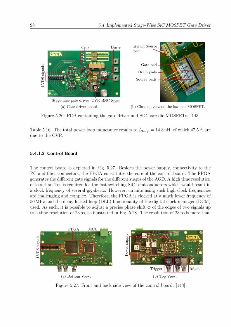
98 5.4 Implemented Stage-Wise SiC MOSFET Gate Driver
SDUT
DDUT
Stage-wise gate driver CVR
LVDSsignals
CDC
BNC
(a) Gate driver board.
Drain pads
Gate pad
Source pads
Kelvin Sourcepad
(b) Close up view on the low-side MOSFET.
Figure 5.26: PCB containing the gate driver and SiC bare die MOSFETs. [143]
Table 5.16. The total power loop inductance results to LLoop = 14.3 nH, of which 47.5 % aredue to the CVR.
5.4.1.2 Control Board
The control board is depicted in Fig. 5.27. Besides the power supply, connectivity to thePC and fiber connectors, the FPGA constitutes the core of the control board. The FPGAgenerates the different gate signals for the different stages of the AGD. A high time resolutionof less than 1 ns is required for the fast switching SiC semiconductors which would result ina clock frequency of several gigahertz. However, circuits using such high clock frequenciesare challenging and complex. Therefore, the FPGA is clocked at a much lower frequency of50 MHz and the delay-locked loop (DLL) functionality of the digital clock manager (DCM)used. As such, it is possible to adjust a precise phase shift ϕ of the edges of two signals upto a time resolution of 23 ps, as illustrated in Fig. 5.28. The resolution of 23 ps is more than
FPGA MCU
LVDSsign
als
(a) Bottom View.
RS232
Pow
ersupply
Trigger
(b) Top View.
Figure 5.27: Front and back side view of the control board. [143]
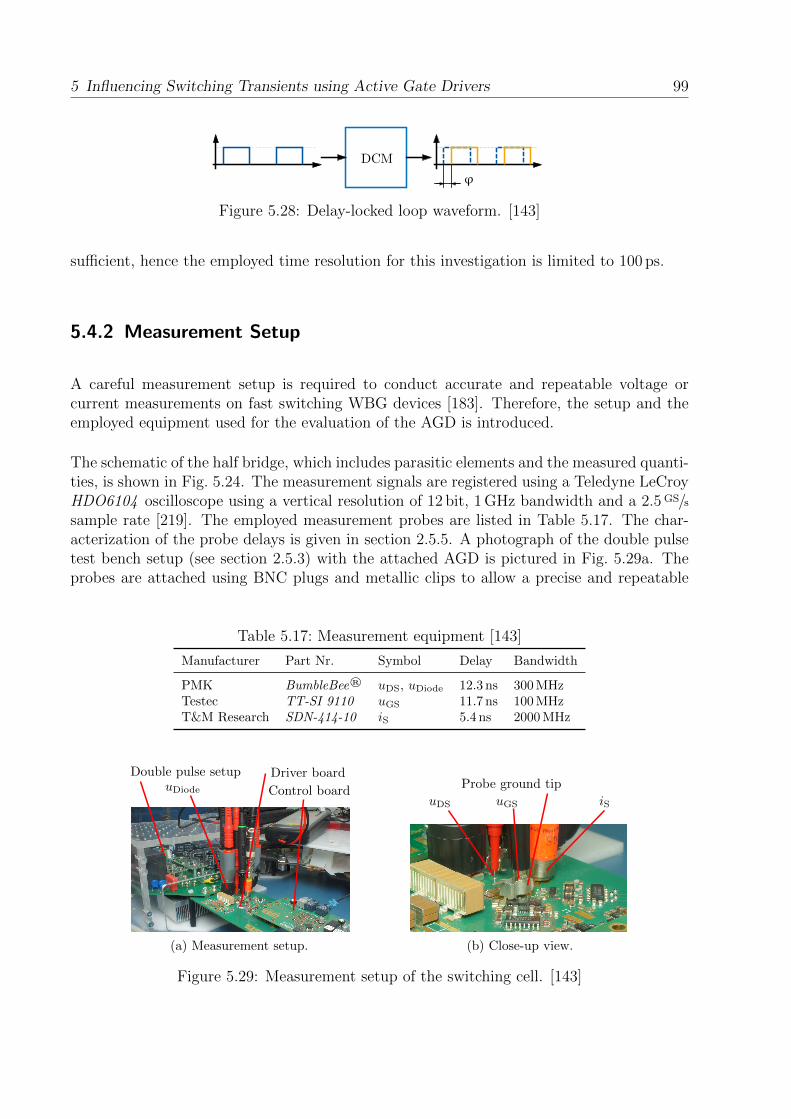
5 Influencing Switching Transients using Active Gate Drivers 99
Son,1
Son,2
Son,3
RonS1
RonS3
RonS2
tonS1
tonS2
tonS3
t
t
t
t
DCM
ϕ
Figure 5.28: Delay-locked loop waveform. [143]
sufficient, hence the employed time resolution for this investigation is limited to 100 ps.
5.4.2 Measurement Setup
A careful measurement setup is required to conduct accurate and repeatable voltage orcurrent measurements on fast switching WBG devices [183]. Therefore, the setup and theemployed equipment used for the evaluation of the AGD is introduced.
The schematic of the half bridge, which includes parasitic elements and the measured quanti-ties, is shown in Fig. 5.24. The measurement signals are registered using a Teledyne LeCroyHDO6104 oscilloscope using a vertical resolution of 12 bit, 1 GHz bandwidth and a 2.5 GS/ssample rate [219]. The employed measurement probes are listed in Table 5.17. The char-acterization of the probe delays is given in section 2.5.5. A photograph of the double pulsetest bench setup (see section 2.5.3) with the attached AGD is pictured in Fig. 5.29a. Theprobes are attached using BNC plugs and metallic clips to allow a precise and repeatable
Table 5.17: Measurement equipment [143]
Manufacturer Part Nr. Symbol Delay Bandwidth
PMK BumbleBee® uDS, uDiode 12.3 ns 300 MHzTestec TT-SI 9110 uGS 11.7 ns 100 MHzT&M Research SDN-414-10 iS 5.4 ns 2000 MHz
uDiode
Driver board
Control board
Double pulse setup
(a) Measurement setup.
uGSuDS iS
Probe ground tip
(b) Close-up view.
Figure 5.29: Measurement setup of the switching cell. [143]
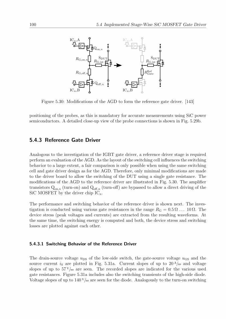
100 5.4 Implemented Stage-Wise SiC MOSFET Gate Driver
SDUTSDUT
Qon,n
Qoff,n
RG,on,n
RG,off,n
ICn,A
RRefGate
ICn,B
ICn,A
ICn,B
RG,int RG,int
Figure 5.30: Modifications of the AGD to form the reference gate driver. [143]
positioning of the probes, as this is mandatory for accurate measurements using SiC powersemiconductors. A detailed close-up view of the probe connections is shown in Fig. 5.29b.
5.4.3 Reference Gate Driver
Analogous to the investigation of the IGBT gate driver, a reference driver stage is requiredperform an evaluation of the AGD. As the layout of the switching cell influences the switchingbehavior to a large extent, a fair comparison is only possible when using the same switchingcell and gate driver design as for the AGD. Therefore, only minimal modifications are madeto the driver board to allow the switching of the DUT using a single gate resistance. Themodifications of the AGD to the reference driver are illustrated in Fig. 5.30. The amplifiertransistors Qon,n (turn-on) and Qoff,n (turn-off) are bypassed to allow a direct driving of theSiC MOSFET by the driver chip ICn.
The performance and switching behavior of the reference driver is shown next. The inves-tigation is conducted using various gate resistances in the range RG = 0.5 Ω . . . 10 Ω. Thedevice stress (peak voltages and currents) are extracted from the resulting waveforms. Atthe same time, the switching energy is computed and both, the device stress and switchinglosses are plotted against each other.
5.4.3.1 Switching Behavior of the Reference Driver
The drain-source voltage uDS of the low-side switch, the gate-source voltage uGS and thesource current iS are plotted in Fig. 5.31a. Current slopes of up to 20 A/ns and voltageslopes of up to 57 V/ns are seen. The recorded slopes are indicated for the various usedgate resistances. Figure 5.31a includes also the switching transients of the high-side diode.Voltage slopes of up to 140 V/ns are seen for the diode. Analogously to the turn-on switching

5 Influencing Switching Transients using Active Gate Drivers 101
RGate = 0.5 Ω RGate = 1.0 Ω RGate = 1.5 Ω RGate = 2.2 ΩRGate = 3.3 Ω RGate = 4.7 Ω RGate = 6.8 Ω RGate = 10 Ω
−50 0 50 100
0
200
400
600
800−57V/ns
−60V/ns
−55V/ns
−46V/ns
−37V/ns
−29V/ns
−25V/ns
−19V/ns
20A/ns16A/ns14A/ns11A/ns8.2A/ns6.4A/ns4.8A/ns3.4A/ns
uDSin
V
i Sin
A
uDS iS
−50 0 50 100
−200
0
200
400
600
800
1,000 135V/ns
109V/ns
93.5V/ns
76V/ns
40.3V/ns
36V/ns
27.4V/ns
19.3V/ns
uDiodein
V
i Diodein
A
uDiode
iDiode
−50 0 50 1000
10
20
Time in ns
uGSin
V
(a) Turn-on event.
−50 0 50 100 150
0
200
400
600
800
69V/ns
66V/ns
62V/ns
57V/ns
49V/ns
39V/ns
31V/ns
24V/ns
−10A/ns−9.3A/ns−9.2A/ns−8.7A/ns−8.6A/ns−7.7A/ns−6.3A/ns−4.4A/ns
uDSin
V
i Sin
A
uDS
iS
−50 0 50 100 150
0
200
400
600
800
−89V/ns−75V/ns−66V/ns−56V/ns−46V/ns−37V/ns−29V/ns−23V/ns
uDiodein
V
i Diodein
AuDiode iDiode
−50 0 50 100 150
0
10
20
Time in ns
uGSin
V
(b) Turn-off event.
Figure 5.31: Measured waveforms using the reference driver. [143]
behavior, the turn-off switching trajectories are plotted in Fig. 5.31b. Voltage slopes of upto 89 V/ns and current slopes of up to 10 A/ns are observed.
5.4.3.2 Switching Performance of the Reference Driver
The extracted switching losses of the turn-on and turn-off event measurements are plottedagainst the gate resistance RG in Fig. 5.32. A linear dependency is seen for the turn-on aswell as for the turn-off energy Eon and Eoff for the investigated gate resistor range.
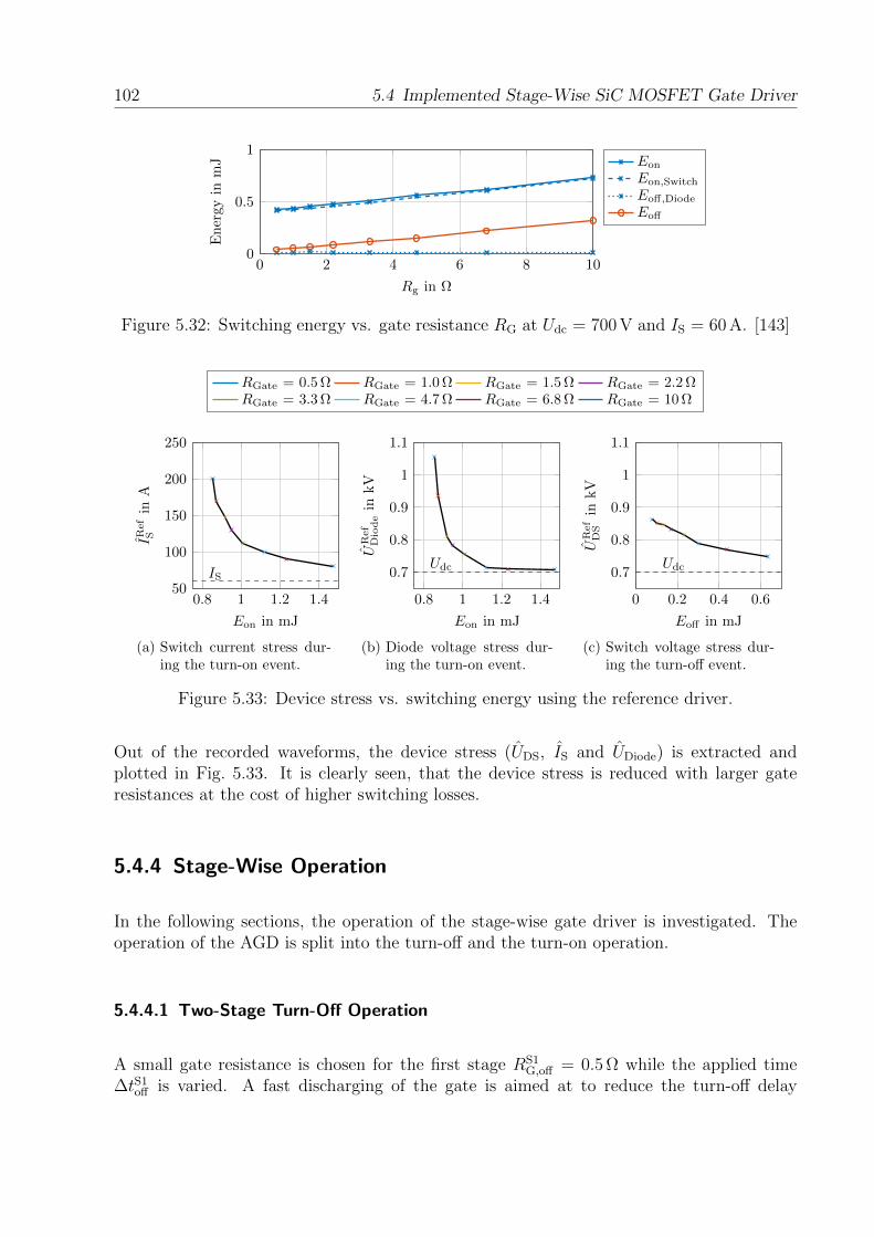
102 5.4 Implemented Stage-Wise SiC MOSFET Gate Driver
0 2 4 6 8 100
0.5
1
Rg in Ω
En
ergy
inm
J Eon
Eon,Switch
Eoff,Diode
Eoff
Figure 5.32: Switching energy vs. gate resistance RG at Udc = 700 V and IS = 60 A. [143]
RGate = 0.5 Ω RGate = 1.0 Ω RGate = 1.5 Ω RGate = 2.2 ΩRGate = 3.3 Ω RGate = 4.7 Ω RGate = 6.8 Ω RGate = 10 Ω
0.8 1 1.2 1.450
100
150
200
250
IS
Eon in mJ
IRef
Sin
A
(a) Switch current stress dur-ing the turn-on event.
0.8 1 1.2 1.4
0.7
0.8
0.9
1
1.1
Udc
Eon in mJ
URef
Diodein
kV
(b) Diode voltage stress dur-ing the turn-on event.
0 0.2 0.4 0.6
0.7
0.8
0.9
1
1.1
Udc
Eoff in mJ
UR
ef
DS
inkV
(c) Switch voltage stress dur-ing the turn-off event.
Figure 5.33: Device stress vs. switching energy using the reference driver.
Out of the recorded waveforms, the device stress (UDS, IS and UDiode) is extracted andplotted in Fig. 5.33. It is clearly seen, that the device stress is reduced with larger gateresistances at the cost of higher switching losses.
5.4.4 Stage-Wise Operation
In the following sections, the operation of the stage-wise gate driver is investigated. Theoperation of the AGD is split into the turn-off and the turn-on operation.
5.4.4.1 Two-Stage Turn-Off Operation
A small gate resistance is chosen for the first stage RS1G,off = 0.5 Ω while the applied time
∆tS1off is varied. A fast discharging of the gate is aimed at to reduce the turn-off delay
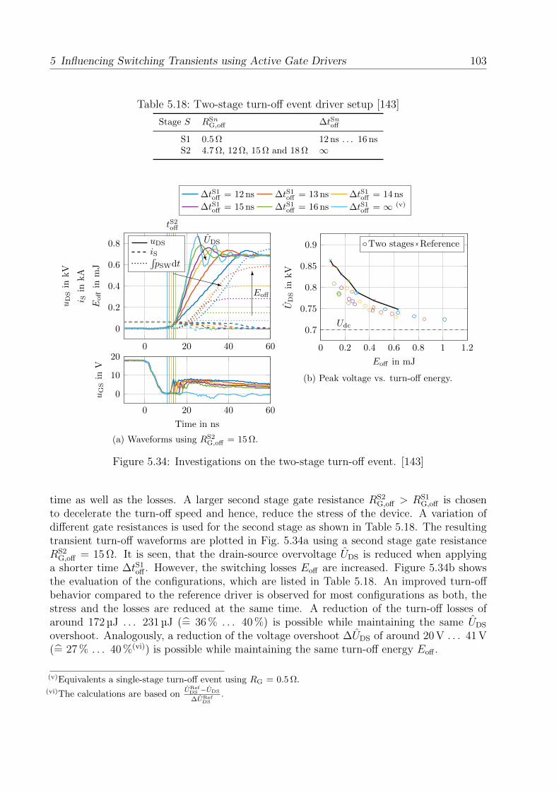
5 Influencing Switching Transients using Active Gate Drivers 103
Table 5.18: Two-stage turn-off event driver setup [143]
Stage S RSnG,off ∆tSnoff
S1 0.5 Ω 12 ns . . . 16 nsS2 4.7 Ω, 12 Ω, 15 Ω and 18 Ω ∞
Rg,off,2 = 15 Ω∆tS1
off = 12 ns ∆tS1off = 13 ns ∆tS1
off = 14 ns
∆tS1off = 15 ns ∆tS1
off = 16 ns ∆tS1off = ∞ (v)
0 20 40 60
0
0.2
0.4
0.6
0.8
uD
Sin
kV
i Sin
kA
Eoffin
mJ
uDS
iSpSWdtXXXXXXz
6
BBBN
Eoff
UDS
tS2off
0 20 40 60
0
10
20
Time in ns
uGSin
V
(a) Waveforms using RS2G,off = 15 Ω.
0 0.2 0.4 0.6 0.8 1 1.2
0.7
0.75
0.8
0.85
0.9
Udc
Eoff in mJ
UD
Sin
kV
Two stages Reference
(b) Peak voltage vs. turn-off energy.
Figure 5.34: Investigations on the two-stage turn-off event. [143]
time as well as the losses. A larger second stage gate resistance RS2G,off > RS1
G,off is chosento decelerate the turn-off speed and hence, reduce the stress of the device. A variation ofdifferent gate resistances is used for the second stage as shown in Table 5.18. The resultingtransient turn-off waveforms are plotted in Fig. 5.34a using a second stage gate resistanceRS2
G,off = 15 Ω. It is seen, that the drain-source overvoltage UDS is reduced when applyinga shorter time ∆tS1
off . However, the switching losses Eoff are increased. Figure 5.34b showsthe evaluation of the configurations, which are listed in Table 5.18. An improved turn-offbehavior compared to the reference driver is observed for most configurations as both, thestress and the losses are reduced at the same time. A reduction of the turn-off losses ofaround 172 µJ . . . 231 µJ (= 36 % . . . 40 %) is possible while maintaining the same UDS
overshoot. Analogously, a reduction of the voltage overshoot ∆UDS of around 20 V . . . 41 V(= 27 % . . . 40 %(vi)) is possible while maintaining the same turn-off energy Eoff .
(v)Equivalents a single-stage turn-off event using RG = 0.5 Ω.(vi)The calculations are based on
URefDS −UDS
∆URefDS
.
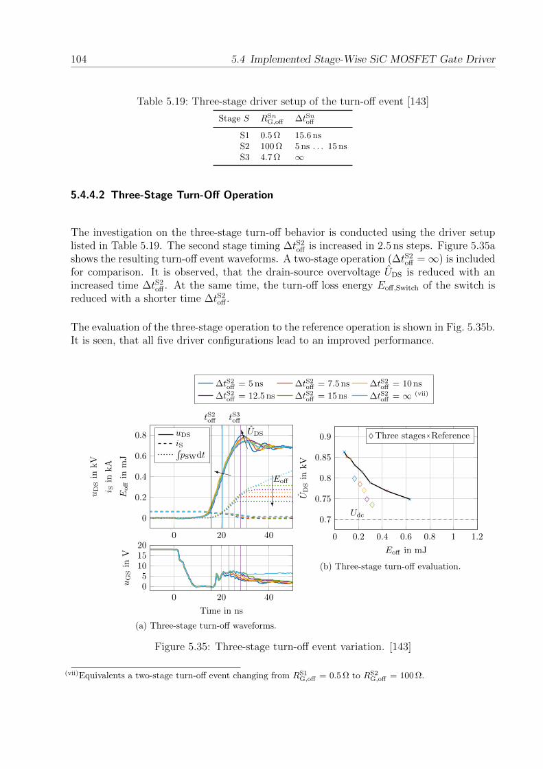
104 5.4 Implemented Stage-Wise SiC MOSFET Gate Driver
Table 5.19: Three-stage driver setup of the turn-off event [143]
Stage S RSnG,off ∆tSnoff
S1 0.5 Ω 15.6 nsS2 100 Ω 5 ns . . . 15 nsS3 4.7 Ω ∞
5.4.4.2 Three-Stage Turn-Off Operation
The investigation on the three-stage turn-off behavior is conducted using the driver setuplisted in Table 5.19. The second stage timing ∆tS2
off is increased in 2.5 ns steps. Figure 5.35ashows the resulting turn-off event waveforms. A two-stage operation (∆tS2
off =∞) is includedfor comparison. It is observed, that the drain-source overvoltage UDS is reduced with anincreased time ∆tS2
off . At the same time, the turn-off loss energy Eoff,Switch of the switch isreduced with a shorter time ∆tS2
off .
The evaluation of the three-stage operation to the reference operation is shown in Fig. 5.35b.It is seen, that all five driver configurations lead to an improved performance.
∆tS1off = 15.6 ns
∆tS2off = 5 ns ∆tS2
off = 7.5 ns ∆tS2off = 10 ns
∆tS2off = 12.5 ns ∆tS2
off = 15 ns ∆tS2off = ∞ (vii)
0 20 40
0
0.2
0.4
0.6
0.8
uD
Sin
kV
i Sin
kA
Eoffin
mJ
uDS
iSpSWdt
XXy
?
BBBM
Eoff
UDS
tS2off tS3
off
0 20 4005101520
Time in ns
uGSin
V
(a) Three-stage turn-off waveforms.
0 0.2 0.4 0.6 0.8 1 1.2
0.7
0.75
0.8
0.85
0.9
Udc
Eoff in mJ
UD
Sin
kV
Three stages Reference
(b) Three-stage turn-off evaluation.
Figure 5.35: Three-stage turn-off event variation. [143]
(vii)Equivalents a two-stage turn-off event changing from RS1G,off = 0.5 Ω to RS2
G,off = 100 Ω.
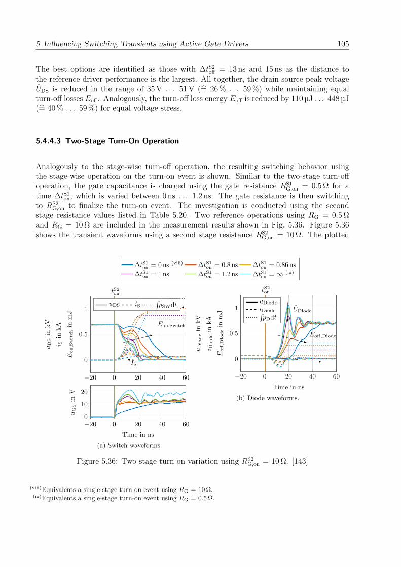
5 Influencing Switching Transients using Active Gate Drivers 105
The best options are identified as those with ∆tS2off = 13 ns and 15 ns as the distance to
the reference driver performance is the largest. All together, the drain-source peak voltageUDS is reduced in the range of 35 V . . . 51 V (= 26 % . . . 59 %) while maintaining equalturn-off losses Eoff . Analogously, the turn-off loss energy Eoff is reduced by 110 µJ . . . 448 µJ(= 40 % . . . 59 %) for equal voltage stress.
5.4.4.3 Two-Stage Turn-On Operation
Analogously to the stage-wise turn-off operation, the resulting switching behavior usingthe stage-wise operation on the turn-on event is shown. Similar to the two-stage turn-offoperation, the gate capacitance is charged using the gate resistance RS1
G,on = 0.5 Ω for atime ∆tS1
on, which is varied between 0 ns . . . 1.2 ns. The gate resistance is then switchingto RS2
G,on to finalize the turn-on event. The investigation is conducted using the secondstage resistance values listed in Table 5.20. Two reference operations using RG = 0.5 Ωand RG = 10 Ω are included in the measurement results shown in Fig. 5.36. Figure 5.36shows the transient waveforms using a second stage resistance RS2
G,on = 10 Ω. The plotted
10∆tS1on = 0 ns (viii) ∆tS1on = 0.8 ns ∆tS1on = 0.86 ns
∆tS1on = 1 ns ∆tS1on = 1.2 ns ∆tS1on = ∞ (ix)
−20 0 20 40 60
0
0.5
1
uDSin
kV
i Sin
kA
Eon,Switch
inmJ
uDS iS´
pSWdt
:
6
?
Eon,Switch
IS
tS2on
−20 0 20 40 600
10
20
Time in ns
uGSin
V
(a) Switch waveforms.
−20 0 20 40 60
0
0.5
1
Time in ns
uD
iodein
kV
i Dio
dein
kA
Eoff,D
iodein
mJ
uDiode
iDiode´
pDdt
XXXXXz
?
?
Eoff,Diode
UDiode
tS2on
(b) Diode waveforms.
Figure 5.36: Two-stage turn-on variation using RS2G,on = 10 Ω. [143]
(viii)Equivalents a single-stage turn-on event using RG = 10 Ω.(ix)Equivalents a single-stage turn-on event using RG = 0.5 Ω.
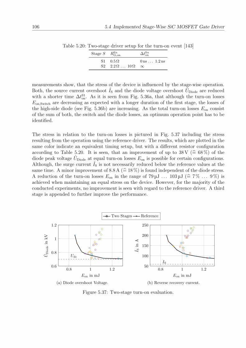
106 5.4 Implemented Stage-Wise SiC MOSFET Gate Driver
Table 5.20: Two-stage driver setup for the turn-on event [143]
Stage S RSnG,on ∆tSnon
S1 0.5 Ω 0 ns . . . 1.2 nsS2 2.2 Ω . . . 10 Ω ∞
measurements show, that the stress of the device is influenced by the stage-wise operation.Both, the source current overshoot IS and the diode voltage overshoot UDiode are reducedwith a shorter time ∆tS1
on. As it is seen from Fig. 5.36a, that although the turn-on lossesEon,Switch are decreasing as expected with a longer duration of the first stage, the losses ofthe high-side diode (see Fig. 5.36b) are increasing. As the total turn-on losses Eon consistof the sum of both, the switch and the diode losses, an optimum operation point has to beidentified.
The stress in relation to the turn-on losses is pictured in Fig. 5.37 including the stressresulting from the operation using the reference driver. The results, which are plotted in thesame color indicate an equivalent timing setup, but with a different resistor configurationaccording to Table 5.20. It is seen, that an improvement of up to 38 V (= 68 %) of thediode peak voltage UDiode at equal turn-on losses Eon is possible for certain configurations.Although, the surge current IS is not necessarily reduced below the reference values at thesame time. A minor improvement of 8.8 A (= 18 %) is found independent of the diode stress.A reduction of the turn-on losses Eon in the range of 79 µJ . . . 103 µJ (= 7 % . . . 9 %) isachieved when maintaining an equal stress on the device. However, for the majority of theconducted experiments, no improvement is seen with regard to the reference driver. A thirdstage is appended to further improve the performance.
Two Stages Reference
0.8 1 1.20.6
0.8
1
1.2
Udc
Eon in mJ
UDiodein
kV
(a) Diode overshoot Voltage.
0.8 1 1.250
100
150
200
250
IS
Eon in mJ
I Sin
A
(b) Reverse recovery current.
Figure 5.37: Two-stage turn-on evaluation.
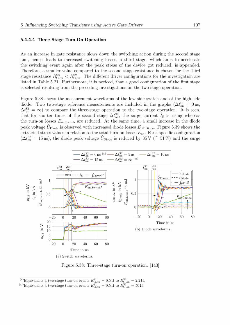
5 Influencing Switching Transients using Active Gate Drivers 107
5.4.4.4 Three-Stage Turn-On Operation
As an increase in gate resistance slows down the switching action during the second stageand, hence, leads to increased switching losses, a third stage, which aims to acceleratethe switching event again after the peak stress of the device got reduced, is appended.Therefore, a smaller value compared to the second stage resistance is chosen for the thirdstage resistance RS3
G,on < RS2G,on. The different driver configurations for the investigation are
listed in Table 5.21. Furthermore, it is noticed, that a good configuration of the first stageis selected resulting from the preceding investigations on the two-stage operation.
Figure 5.38 shows the measurement waveforms of the low-side switch and of the high-sidediode. Two two-stage reference measurements are included in the graphs (∆tS1
on = 0 ns,∆tS1
on = ∞) to compare the three-stage operation to the two-stage operation. It is seen,that for shorter times of the second stage ∆tS2
on, the surge current IS is rising whereasthe turn-on losses Eon,Switch are reduced. At the same time, a small increase in the diode
peak voltage UDiode is observed with increased diode losses Eoff,Diode. Figure 5.39 shows theextracted stress values in relation to the total turn-on losses Eon. For a specific configuration(∆tS2
on = 15 ns), the diode peak voltage UDiode is reduced by 35 V (= 51 %) and the surge
∆tS2on = 0.86 ns∆tS2on = 0 ns (x) ∆tS2on = 5 ns ∆tS2on = 10 ns
∆tS2on = 15 ns ∆tS2on = ∞ (xi)
−20 0 20 40 60 80
0
0.5
1
uDSin
kV
i Sin
kA
Eon,Switch
inmJ
uDS iS´
pSWdt
9
?
6
Eon,Switch
IS
tS2on tS3
on
−20 0 20 40 60 8005101520
Time in ns
uGSin
V
(a) Switch waveforms.
−20 0 20 40 60 80
0
0.5
1
Time in ns
uD
iodein
kV
i Dio
dein
kA
Eoff,D
iodein
mJ
uDiode
iDiode´
pDdt
XXXXy
6
JJJ]
Eoff,Diode
UDiode
tS2on tS3
on
(b) Diode waveforms.
Figure 5.38: Three-stage turn-on operation. [143]
(x)Equivalents a two-stage turn-on event: RS1G,on = 0.5 Ω to RS2
G,on = 2.2 Ω.(xi)Equivalents a two-stage turn-on event: RS1
G,on = 0.5 Ω to RS2G,on = 50 Ω.
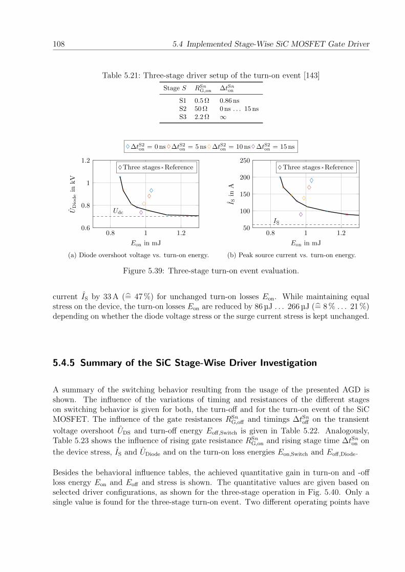
108 5.4 Implemented Stage-Wise SiC MOSFET Gate Driver
Table 5.21: Three-stage driver setup of the turn-on event [143]
Stage S RSnG,on ∆tSnon
S1 0.5 Ω 0.86 nsS2 50 Ω 0 ns . . . 15 nsS3 2.2 Ω ∞
∆tS2on = 0 ns ∆tS2on = 5 ns ∆tS2on = 10 ns ∆tS2on = 15 ns
0.8 1 1.20.6
0.8
1
1.2
Udc
Eon in mJ
UDiodein
kV
Three stages Reference
(a) Diode overshoot voltage vs. turn-on energy.
0.8 1 1.250
100
150
200
250
IS
Eon in mJ
I Sin
A
Three stages Reference
(b) Peak source current vs. turn-on energy.
Figure 5.39: Three-stage turn-on event evaluation.
current IS by 33 A (= 47 %) for unchanged turn-on losses Eon. While maintaining equalstress on the device, the turn-on losses Eon are reduced by 86 µJ . . . 266 µJ (= 8 % . . . 21 %)depending on whether the diode voltage stress or the surge current stress is kept unchanged.
5.4.5 Summary of the SiC Stage-Wise Driver Investigation
A summary of the switching behavior resulting from the usage of the presented AGD isshown. The influence of the variations of timing and resistances of the different stageson switching behavior is given for both, the turn-off and for the turn-on event of the SiCMOSFET. The influence of the gate resistances RSn
G,off and timings ∆tSnoff on the transient
voltage overshoot UDS and turn-off energy Eoff,Switch is given in Table 5.22. Analogously,Table 5.23 shows the influence of rising gate resistance RSn
G,on and rising stage time ∆tSnon on
the device stress, IS and UDiode and on the turn-on loss energies Eon,Switch and Eoff,Diode.
Besides the behavioral influence tables, the achieved quantitative gain in turn-on and -offloss energy Eon and Eoff and stress is shown. The quantitative values are given based onselected driver configurations, as shown for the three-stage operation in Fig. 5.40. Only asingle value is found for the three-stage turn-on event. Two different operating points have
5 Influencing Switching Transients using Active Gate Drivers 109
Table 5.22: Summary of the SiC MOSFET turn-off behavior [143]
UDS Eoff Reference
RS1G,off↑ Fig. 5.32, Fig. 5.33
∆tS1off ↑ Fig. 5.34
RS2G,off↑ Fig. 5.34b
∆tS2off ↑ Fig. 5.35
RS3G,off↑ — (xii)
Table 5.23: Summary of the SiC MOSFET turn-on behavior [143]
IS UDiode Eon,Switch Eoff,Diode Eon Reference
RS1G,on↑ → Fig. 5.32, Fig. 5.33
∆tS1on ↑ Fig. 5.36
RS2G,on↑ Fig. 5.36, Fig. 5.37
∆tS2on ↑ Fig. 5.38
RS3G,on↑ — — (xii)
been chosen for the turn-off event (A & B) because a best configuration is not defined. Theconfiguration A represents a configuration allowing fast switching speed, while the config-uration B represents a more moderate switching speed, however with an increased stressand loss reduction compared to configuration A. For each selected point, the horizontaldistance to the curve of the reference driver is measured to find the reduction of switchinglosses while maintaining an equal stress. The vertical distance defines the stress reductionfor unchanged switching losses. Two different points are investigated for the turn-off event,to have a representative of a fast and slower switching configuration. The extracted valuesfor constant stress are summarized in Table 5.24, whereas the values for reduced stress atconstant switching losses Eon and Eoff are shown in Table 5.25.
Table 5.24: Resulting loss improvements for equal device stress
Two stages Three stagesRelative Absolute Relative Absolute
Eoff 36 % . . . 40 % 172 µJ . . . 231 µJ 40 % . . . 59 % 108 µJ . . . 442 µJEon 7 % . . . 9 % 79 µJ . . . 103 µJ 8 % . . . 21 % 86 µJ . . . 266 µJ
(xii)The influence of the third stage resistance has to be investigated experimentally in future work. Theindicated behavior is justified with a slower current or voltage decay with larger gate resistance, which inturn is responsible for higher losses.
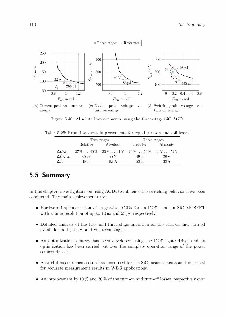
110 5.5 Summary
Three stages Reference
0.8 1 1.250
100
150
200
250
IS
Eon in mJ
I Sin
A
33 A
266 µJ
(b) Current peak vs. turn-onenergy.
0.8 1 1.2
700
800
900
Eon in mJ
UDiodein
V
36 V
86 µJ
(c) Diode peak voltage vs.turn-on energy.
0 0.2 0.4 0.6 0.8
700
800
900
Eoff in mJ
UD
Sin
V
34 V 108 µJA
B52 V
442 µJ
(d) Switch peak voltage vs.turn-off energy.
Figure 5.40: Absolute improvements using the three-stage SiC AGD.
Table 5.25: Resulting stress improvements for equal turn-on and -off losses
Two stages Three stagesRelative Absolute Relative Absolute
∆UDS 27 % . . . 40 % 20 V . . . 41 V 26 % . . . 60 % 34 V . . . 52 V
∆UDiode 68 % 38 V 49 % 36 V
∆IS 18 % 8.8 A 53 % 33 A
5.5 Summary
In this chapter, investigations on using AGDs to influence the switching behavior have beenconducted. The main achievements are:
• Hardware implementation of stage-wise AGDs for an IGBT and an SiC MOSFETwith a time resolution of up to 10 ns and 23 ps, respectively.
• Detailed analysis of the two- and three-stage operation on the turn-on and turn-offevents for both, the Si and SiC technologies.
• An optimization strategy has been developed using the IGBT gate driver and anoptimization has been carried out over the complete operation range of the powersemiconductor.
• A careful measurement setup has been used for the SiC measurements as it is crucialfor accurate measurement results in WBG applications.
• An improvement by 10 % and 30 % of the turn-on and turn-off losses, respectively over

5 Influencing Switching Transients using Active Gate Drivers 111
the complete operating range has been achieved for equal stress on the IGBT.
• A reduction of stress and switching losses has been shown using the SiC power semicon-ductor. The results show, that for example a reduction of up to 60 % of the overshootvoltage ∆UDS is achievable without influencing the turn-off losses. Analogously, it hasbeen shown that the turn-off energy is reduced by up to 59 % for equal device stress.
The conclusions, which are drawn from the conducted investigations are:
• A similar behavior and improvement opportunity has been observed for both semi-conductor technologies.
• It has been shown, that two stages are not sufficient to reach an improved switchingbehavior with reduced stress and reduced losses at the same time. At least three stagesare required to achieve a gain in stress and loss energies.
• The stage-wise driver for SiC showed that a feedback loop is hardly achievable dueto the long delay times from the driver action to a visible result in the switchingtransients.

112

6 Unifying the Active Gate Driver with theSwitching Cell Design
In the preceding chapters, the impact of individual stray inductances (see chapter 4) and ofactive gate drivers (see chapter 5) on the switching performance has been investigated inten-sively. Both investigations have resulted in reduced electrical stress and reduced switchingenergies. This chapter brings the results of both investigations together. It is shown, thatthe AGD is able to effectively reduce the effect of DBC design compromises yielding a supe-rior switching performance. Design compromises are arising due to third party constraints,such as manufacturability, thermal design or production costs.
6.1 Findings from the Active Gate Drivers
The findings from the active gate driver investigations on the transient switching behaviorare discussed first. A separate discussion is conducted for the gate driver using the IGBTpower module and the SiC MOSFET because only a single operating point has been focusedon using the SiC AGD, while a the complete operating area has been investigated using theSi IGBT gate driver.
6.1.1 Findings from the Active Gate Driver for Si IGBTs
The investigations using a stage-wise active gate driver for Si IGBTs resulted in reducedstress for the power semiconductor while maintaining equal switching energies. Analogously,using different configurations of the AGD, reduced switching energies have been achievedwhile maintaining the device stress at the reference level. These investigations have beenconducted over the whole operating range of the power device, including voltage, currentand temperature leading to the results listed in Table 5.12.
As more or less similar improvements are found for each individual operating point, it isassumed that it is valid to extrapolate the investigations on a single operating point usingthe AGD for SiC MOSFETs to the whole operating range.
113

114 6.2 Findings of the Parasitic Inductance Investigations
Table 6.1: Stress reduction using the SiC AGD at equal switching losses
Quantity Improvement
UDS 34 V and 52 V
UDiode 36 V
IS 33 A
6.1.2 Findings from the Active Gate Driver for SiC MOSFETs
Analog to the Si IGBT gate driver, similar improvements concerning reduced switchinglosses and reduced device stress have been found using the AGD for SiC MOSFETs. It isnoticed, that unlike for the investigations on the IGBT AGD, the investigations using theSiC MOSFET AGD have not been optimized. The shown results have therefore furtherpotential for improvement. Nevertheless, satisfying results have been achieved, as shown insection 5.4.5.
For the following evaluations, the reduction of stress without changing the switching lossesis of interest. Table 6.1 summarizes the stress reductions, which have been pictured inFig. 5.40. Three consequences are concluded from the reduced stress of the power semicon-ductor:
1. Using less SiC material for a lower voltage rated power semiconductor and thus re-ducing the material costs of a given converter.
2. The usage of a higher dc-link voltage, and therewith increasing the power density ofthe converter.
3. Counteract or cancel the effect of DBC design compromises on the switching perfor-mance.
The latter option is investigated further in the following section.
6.2 Findings of the Parasitic Inductance Investigations
Chapter 4 investigated on the influence of five different parasitic inductances from the switch-ing cell layout on the switching performance. Besides the low- and high-side common-sourceinductances and the low- and high-side gate inductances, the power loop inductance has amajor influence on the device stress. The investigations have been conducted for two scenar-ios: a very fast switching speed setup using a gate resistance RG,LS = 0 Ω and a setup usinga more moderate switching speed using a gate resistance RG,LS = 5.6 Ω. For the followingevaluation, only the moderate switching speed setup is of interest because the average gate
6 Unifying the Active Gate Driver with the Switching Cell Design 115
resistance during a switching transient using the active gate driver is in the same range orhigher.
6.2.1 Gate and Common-Source Inductances
The effect of the gate and common-source inductances on the switching performance, whichare relevant, are summarized in Table 4.4. The high-side parasitic inductances (LG,HS andLCS,HS) are neglected as they have no noticeable influence on the switching behavior. Thelow-side parasitic inductances (LG,LS and LCS,HS) reduce the stress on the device whileincreasing the switching energies. The active gate driver could be used in combination witha certain gate inductance to reduce the switching losses, hence achieve an improved switchingperformance with a given gate inductance, which is due to third party constraints. However,from the gate driver point of view, the common-source inductance counts as additional gateinductance including a feedback from the transient source current. The SiC AGD is designedand evaluated using a Kelvin source contact together with a low inductive gate path to ensurea highly dynamic influence on the switching transients. Further investigations are requiredin future work, to validate the AGD with higher inductive gate paths.
6.2.2 Power Loop Inductance
The power loop inductance has a high impact on the voltage stress of the power semiconduc-tor but only a minor impact on the total switching losses Esw, as seen in Table 4.4. From anelectrical point of view, the power loop inductance should be designed as small as possible.However, the power loop inductance is primarily defined by third party constraints, suchas the mechanical and thermal design of a power module, which consequently leads to adeterioration of the switching performance. This is where the active gate drivers come intoplay. As it has been shown previously, the active gate driver is able to reduce the devicestress while maintaining equal switching losses. Thus, the question is, how much an activegate driver can compensate for increased power loop inductance without having an impacton the switching losses.
The relation between device stress and power loop inductance has been evaluated inten-sively in Fig. A.17, Fig. A.18, Fig. A.19 and Fig. 4.10. A linear relation is found betweenthe stress and power loop inductance. In the employed setup on the parasitic inductancesinvestigations, the smallest power loop inductance is LLoop = 25 nH, which is due to thevarious inductance variation setups and additional stray inductances (e.g., the CVR induc-tance Lσ,CVR). However, state of the art optimized SiC switching cells achieve power loopinductances below 10 nH down to the subnano-henry range [93], [158], [165], [168], [169],[171]. Therefore, an extrapolation of the conducted measurements down to zero power loopinductance is required. Figure 6.1 shows the device stress versus power loop inductance
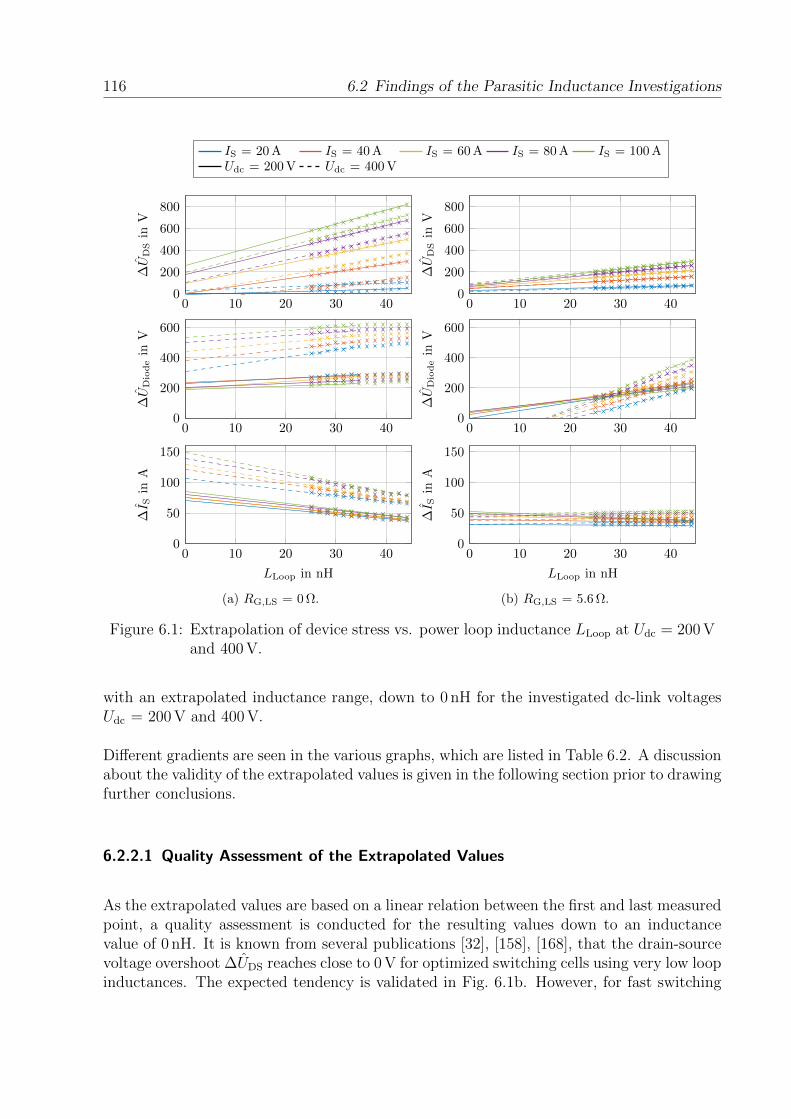
116 6.2 Findings of the Parasitic Inductance Investigations
IS = 20A IS = 40A IS = 60A IS = 80A IS = 100AUdc = 200V Udc = 400V
0 10 20 30 400
200
400
600
800
∆UDS
inV
0 10 20 30 400
200
400
600
∆UDiode
inV
0 10 20 30 400
50
100
150
LLoop in nH
∆I S
inA
(a) RG,LS = 0 Ω.
0 10 20 30 400
200
400
600
800
∆UDS
inV
0 10 20 30 400
200
400
600
∆UDiode
inV
0 10 20 30 400
50
100
150
LLoop in nH
∆I S
inA
(b) RG,LS = 5.6 Ω.
Figure 6.1: Extrapolation of device stress vs. power loop inductance LLoop at Udc = 200 Vand 400 V.
with an extrapolated inductance range, down to 0 nH for the investigated dc-link voltagesUdc = 200 V and 400 V.
Different gradients are seen in the various graphs, which are listed in Table 6.2. A discussionabout the validity of the extrapolated values is given in the following section prior to drawingfurther conclusions.
6.2.2.1 Quality Assessment of the Extrapolated Values
As the extrapolated values are based on a linear relation between the first and last measuredpoint, a quality assessment is conducted for the resulting values down to an inductancevalue of 0 nH. It is known from several publications [32], [158], [168], that the drain-sourcevoltage overshoot ∆UDS reaches close to 0 V for optimized switching cells using very low loopinductances. The expected tendency is validated in Fig. 6.1b. However, for fast switching
6 Unifying the Active Gate Driver with the Switching Cell Design 117
Table 6.2: Relation between device stress and power loop inductance LLoop
Quantity RG,LS = 0 Ω RG,LS = 5.6 Ω
UDS 1.3 V/nH . . . 12.7 V/nH 1.1 V/nH . . . 5 V/nH
UDiode 1.2 V/nH . . . 4.6 V/nH 3.5 V/nH . . . 13.4 V/nH
IS −0.7 A/nH . . . −1.6 A/nH −0.3 A/nH . . . 0.1 A/nH
transients, even very low-inductive switching cells have a certain overshoot voltage [168,Fig. 12 and Fig. 13]. This behavior is also seen in the extrapolated values for the fastswitching operation in Fig. 6.1a.
The voltage overshoot across the high-side diode is, similar to the low-side drain-sourcevoltage, due to the stored energy in the stray inductance. The extrapolated values of themeasurements using Udc = 200 V and RG,LS = 5.6 Ω (see Fig. 6.1b) validate the expectedlinear link, whereas a faster decaying is observed for higher dc-link voltages. As the high-sidediode voltage behavior is poorly documented in literature, no estimations are available foran optimized switching cell. A certain residual voltage overshoot (> 200 V) is expected forthe fast switching operation (RG,LS = 0 Ω) because no mechanism is currently known, whichshould suddenly further reduce the peak voltage with reduced power loop inductance.
A rising surge current IS is observed for increased switching speed. For fast switching events(RG,LS = 0 Ω), the power loop inductance has a major impact on the switching slopes (i.e.,switching speed), therefore a rising surge current is seen in Fig. 6.1a. Due to a higher gateresistance, slower switching speeds are achieved and thus, the switching slopes are linkedto the gate resistance and not on the power loop inductance anymore. Thus, the loopinductance is expected not to have a big influence on the surge current, as confirmed inFig. 6.1b.
Altogether, the extrapolated values are assumed to be valid. They are used in the followingsection to estimate the impact of an active gate driver on the switching performance.
6.3 Improvement Capabilities using Active Gate Drivers
Using the established relations between power loop inductance and stress on the device, itis possible to establish predictions regarding a combined use of AGDs and power modules.A quantitative estimation on how much additional power loop inductance an AGD cancompensate for, is given.
The achieved stress reductions using the AGD (see Table 6.1) are combined with the re-lation between the device stress and power loop inductance (see Table 6.2) leads to theequivalent inductance values listed in Table 6.3. This means, that it possible to compensate

118 6.4 Summary
Table 6.3: Additional allowed power loop inductance when using an AGD
QuantityEquivalence in powerloop inductance
Comment
UDS
34 V/5 V/nH = 6.8 nH faster switching speed (AGD configuration A)52 V/5 V/nH = 10 nH slower switching speed (AGD configuration B)
UDiode
36 V/3.5 V/nH = 10 nH36 V/13.4 V/nH = 2.7 nH only reliable at high power loop inductances
IS —
for an additional 6.8 nH . . . 10 nH power loop inductance using an AGD. Thus, an improvedthermal design, reduced cost or simplified manufacturability can be chosen, while achievingthe same or even increased switching performance. An additional benefit of using an AGDis the additionally reduced reverse recovery peak current during the turn-on event as thepower loop inductance does not have an influence hereon. A reduction of surge current leadsto reduced thermal stress and hence, has a positive impact on the reliability and lifetime ofthe power module [57].
6.4 Summary
This chapter investigates on the outcomes of using active gate drivers to effectively reducethe effect of DBC design compromises yielding a superior switching performance. The activegate driver is used to reduce the voltage stress while maintaining the switching losses at thesame level. At the same time, a linear relation between the voltage stress and the power loopinductance is established. A variation of the power loop inductance does not influence thetotal switching losses. Therefore, the compromise of higher power loop inductance can bechosen in combination with an active gate driver to achieve a superior switching performance.Based on the numerical values, which are derived from the experimental investigations, itis found, that an increase of the power loop inductance by up to 10 nH can be compensatedusing an active gate driver.
7 Conclusions and Outlook
This thesis investigated on the simulative and experimental extraction of the parasitic ele-ments from power modules and the impact of the latter on the switching behavior. Besidesthe parasitic elements, the impact of AGDs on the switching performance has been investi-gated thoroughly for an IGBT and a SiC MOSFET. The switching performance representsthe peak voltage and peak current stress on the device during the switching transients inrelation to the generated switching losses. An increased peak current implies an increasedthermal stress on the device, while an increased peak voltage is critical due to the breakdownvoltage of the semiconductor.
Methodology for Parasitic Elements Extraction
Different methodologies to extract the parasitic capacitances and inductances of the vari-ous switching cells have been proposed and investigated. FE simulations and experimentalapproaches have been shown and validated using two application examples. In particular,various methodologies have been developed for the partial inductance measurements. Whileimpedance and double pulse measurements can be used for specific inductances, a techniqueusing a current pulse generator has been developed as a universal partial inductance mea-surement tool, applicable to any given geometry. A good match between simulated andmeasured values has been found and was further validated by comparing a time domainpower module model against double pulse measurements.
Impact of Parasitic Inductive Elements on the Switching Transients
The impact of various different inductive elements on the switching behavior of SiC powerMOSFETs has been investigated experimentally. To exclude any impact of the switching celllayout, driver, etc. from the investigations, a test board has been developed, which allows toconduct all the investigations using a single setup. In total, five different variable inductanceshave been installed: the power loop inductance, the low- and high-side gate inductance andthe low- and high-side common-source inductance. The variable inductances got realizedusing pin headers allowing a wide range of different inductance values with a step size ofless than 1 nH. The device stress and the switching losses have been extracted from thedouble pulse measurements and evaluated against each other to identify the influence of thedifferent parasitic inductances.
119

120
The major findings for the different inductive elements are:
1. Power loop inductance LLoop:It has been found, that an increase in power loop inductance shifts the turn-on en-ergy Eon to the turn-off event while maintaining the total switching losses constant.At the same time, the voltage stress of the power semiconductor at turn-off is in-creased. Furthermore, for very fast switching actions, the power loop inductance actsas a turn-on snubber and therewith limits the rising current slope. The oscillationsfollowing the switching actions have been identified and verified experimentally as aresonance between the power loop inductance and the output capacitance of the powersemiconductor. As such, the resonance frequency is easily calculated for new designsand adequate counter measures against the emitted EMI can be developed. This isfound to be especially interesting for the EMI filter design of SiC based power con-verters, which becomes more challenging due to the voltage dependency of the SiCMOSFET output capacitance.
2. Common-source inductances LCS,LS and LCS,HS:While the high-side common source inductance does not have any influence on thelow-side switching event, it has been found, that a small common-source inductancedampens occurring oscillations. The exact position of a Kelvin source contact shouldbe wisely chosen, eventually including the power source bond wires, which add aninductance in the range of 1 nH.
3. Gate inductances LG,LS and LG,HS:The gate inductance only has a minor influence on the switching performance whenthe switching behavior is dominated by the power loop inductance. However, forslower switching speeds, an increasing gate inductance lowers the switching losseswhile increasing the voltage and current stress of the device during the switchingtransients.
Active Gate Drivers for Silicon and Silicon Carbide PowerSemiconductors and Their Impact on the Switching Transients
A stage-wise gate driver using a switched resistor topology has been developed and imple-mented for a Si IGBT and a SiC MOSFET. A time resolution of up to 10 ns and 23 ps isachieved for the IGBT and the SiC MOSFET driver, respectively. An investigation on theimpact of different timings and gate resistor values on the switching performance has beenconducted. The evaluation concluded that both, the switching energies and the device stressare influenced with the possibility to reduce both quantities at the same time, resulting ina superior switching performance compared to standard gate drivers. It has been shownthat the stress on the high-side diode is a crucial aspect and must be taken into accountto prevent a failure of the power device. Despite higher costs and reliability aspects of the

7 Conclusions and Outlook 121
active gate driver due to the higher part count, the advantages of AGDs are clearly definedwith reduced voltage and current stress and reduced switching losses. On the system level,the reduced stress and switching losses lead to a positive impact on the lifetime of the powersemiconductor. Furthermore, the reduced voltage stress allows either to use higher dc-linkvoltages or reduce the power semiconductor silicon thickness resulting in reduced materialcosts or increased power density of the converter. This becomes especially interesting formedium-voltage SiC power MOSFETs as their manufacturing costs are still very high com-pared to the costs of an active gate driver. An increased power density of medium-voltage,high-power converters is an immediate consequence.
Combination of Active Gate Drivers and Improved Switching CellDesign
The investigations on parasitic inductances and active gate drivers on the the switchingperformance have each resulted in a cost function of device stress versus switching losseswith either the parasitic inductance or the configuration of the AGD as parameter. It hasbeen shown that the use of an AGD allows to compensate the compromises made in thedesign of the DBC substrate due to third party constraints (e.g., manufacturability, thermaldesign, costs). It has been shown that a variation of the power loop inductance only has aninfluence on the stress of the power semiconductor and not on the switching losses and hence,the active gate driver can be effectively used to reduce the stress while keeping the switchinglosses constant. It is a key finding of this work that the investigated active gate driver isable to compensate for around 10 nH of power loop inductance for the given experimentalsetup based on SiC power devices.
Due to the high number of parts of the active gate driver, the costs are high and lifetimeaspects have to be considered compared to a standard gate driver IC. Therefore, a com-promise between increased cost, lifetime aspects, package design and switching performancehas to be made. Using an active gate driver leads to the following advantages:
1. An increased manufacturability of the power module because a larger geometric designrange is accessible or larger, more robust components (e.g., power connectors) can bechosen.
2. Improved thermal design due to larger copper areas, which allow heat spreading,increased thermal capacitance and provide a larger cross section for a reduced thermalresistance.
3. Possibility of current and voltage slope control to counteract isolation faults in machineand inductor windings.
Each of these mentioned arguments necessarily leads to a reduction of costs, either during
122
the manufacturing process or during the operating period. The reduction of cost is fully orpartially used for the higher cost of the AGD. A further reduction of cost of the AGD andincreased lifetime is achieved by integrating the AGD into an ASIC.
The conducted investigations enable an improved design for the future development of dc-dcconverters and machine inverters. Regarding the dc-dc converters, high switching frequen-cies are required to allow the use of small storage elements (capacitors, inductors) andprovide increased dynamics. Using conventional approaches, a DBC substrate design witha very low power loop inductance is required, which is possible using multiple copper layersin ceramic substrates. However, this leads to a high penalty in thermal performance. Thisis where the AGD comes into play as the AGD allows to compensate for a certain amountof power loop inductance and hence, a state of the art double layer DBC substrate can beused again. Additionally, the higher utilization of the power semiconductors leads to anincreased power density, which is enabled by the stress reduction using the AGD. At thesame time, reduced switching losses result from the usage of the AGD, which is a primaryrequirement for converters operating at high switching frequencies.
A higher potential for the use of the AGD in combination with the package design is seen formedium-voltage converters. A medium-voltage package design does not allow a minimizedstray inductance layout because of long creepage distances and isolation constraints. Dueto the higher dc-link voltage, higher switching times at at equal slopes are appearing, whichreduce the requirement of high timing resolutions. As the relation of the cost of these powerdevices to the cost of the AGD is much higher than for low-voltage power devices, the benefitin increased utilization and improved switching performance is much higher. This is espe-cially interesting for medium-voltage multi-port dc-transformers for dc-grid applications,which are operating at high switching frequencies.
Future Work
Power Module Parasitic Elements Analysis and Methodology
The various parasitic parameter extraction methods, which have been developed and imple-mented in chapter 3, require the elaboration of an error estimation. Especially an accuracyand repeatability accuracy of the partial inductance extraction method using the currentpulse generator is of interest. The transient switching simulations of the IGBT power mod-ule have to be evaluated over a wider operating range and verify the correlation to themeasurements. Furthermore, transient switching simulations have to be carried out us-ing the SiC MOSFET. A detailed investigation on the internal structure of the providedsemiconductor models needs to be conducted. To further improve the correlation betweenthe measurements and the simulation results, the exact measurement points and the in-fluence of the measurement probes have to be investigated and included in the simulation
7 Conclusions and Outlook 123
setup. With a good matching of the simulation results to the measurements, the simula-tion setup can be used to conduct complex parameter variation studies, that needed to beaccurately evaluated by experiments in this work and were discussed in chapter 4. Theseresults allow investigations on the module design before manufacturing and enable offlineoptimizations.
Impact of the Parasitic Elements on the Switching Performance
An improvement of the PCB layout allowing an extended range of the inductance variationsdown to smaller values has to be investigated. Furthermore, the resistance of the powerloop path and the gate loop path have to be investigated, as this is expected to have ahigh impact on the attenuation of the oscillations and their peak value. Different dc-linkcapacitor concepts have to investigated, such as for example distributed dc-link capacitorswith very low inductive capacitors directly at the switching cell and larger capacitors withhigher stray inductance on the converter level ensuring system stability.
Active Gate Drivers
The gate driver configurations resulting from the optimization of the different operatingpoints of the IGBT power module have to be analyzed to derive functions for online calcula-tion. An online calculation of the optimized parameters, depending on the actual operatingpoint, allows the realization of the presented AGD in an ASIC. The realization of the AGDin an ASIC results in an increased reliability due to a reduced part count and a reductionof cost in the final application. Analogously, the realization of an online optimization of theSiC gate driver has to be investigated to avoid the intensive and time consuming offline opti-mization. The impact of the resulting switching behavior on the EMI has to be investigated.This would allow an optimization regarding stress, switching losses and EMI.
The AGD has to be implemented for medium-voltage SiC MOSFETs. Due to the increasedcosts of the power semiconductors compared to the gate driver, which remains more orless unchanged compared to the low-voltage implementation, the AGD becomes much moreattractive. An improved switching behavior, which allows a higher utilization of the powersemiconductors using a higher dc-link voltage or a reduction of the EMI filters due to reducedemissions, is a big advantage for medium-voltage, high-power applications. The usage ofAGDs is especially interesting in medium-voltage, high-power SiC based grid converters,where high power-loop inductances are unavoidable. Furthermore, an implementation of theAGD for GaN power devices is of interest to verify if the same potential for improvementsexists.

124
Combination of the Active Gate Driver and the Power Module Design
As the conclusions, which have been drawn in chapter 6, are based on a hypothetical com-bination of the AGD and an improved switching cell layout, two or more different powermodules with different power loop inductances have to be realized to proof equal switchingbehavior of all three devices using the AGD. This would confirm the established hypothesesand reinforce the conclusions that have been drawn.
The Final Word
Overall, the author is confident that this work will contribute to the improvement of powermodule design using SiC semiconductors. The findings are especially interesting for fu-ture medium-voltage converters connected to the medium-voltage grid. With help of thepresented investigations, the process of designing power modules will be influenced. Theelectrical performance must be considered in a very early design process to ensure an optimalpower module design.
A Appendix
A.1 Inductance Variation
A.1.1 Variation of the Power Loop Inductance
25 nH 30 nH LLoop 39 nH 44 nH
0 50 100 150 200
0
0.5
1
Voltagein
kV
uDS
uDiode
0 50 100 150 200
0
100
i Sin
A
0 50 100 150 200
0
10
20
Time in ns
uGSin
V
(a) Turn-on event.
0 100 200 300
0
0.5
1
Voltagein
kV
uDiode
uDS
0 100 200 300
0
100
i Sin
A
0 100 200 300
0
10
20
Time in ns
uGSin
V
(b) Turn-off event.
Figure A.1: Switching transients for various low-side loop-inductances LLoop atUdc = 200 V, IS = 100 A, RG,LS = 0 Ω, LG,LS = LG,HS = 4.9 nH andLCS,LS = 0 nH.
125
126 A.1 Inductance Variation
25 nH 30 nH LLoop 39 nH 44 nH
0 50 100 150 2000
0.5
1
Voltagein
kV
uDS
uDiode
0 50 100 150 200
0
100
200
i Sin
A
0 50 100 150 200
0
10
20
Time in ns
uGSin
V
(a) Turn-on event.
0 100 200 3000
0.5
1
Voltagein
kV
uDiode
uDS
0 100 200 300
0
100
200
i Sin
A0 100 200 300
0
10
20
Time in nsuGSin
V
(b) Turn-off event.
Figure A.2: Switching transients for various low-side loop-inductances LLoop atUdc = 400 V, IS = 100 A, RG,LS = 0 Ω, LG,LS = LG,HS = 4.9 nH andLCS,LS = 0 nH.
25 nH 30 nH LLoop 39 nH 44 nH
0 50 100 150 200
0
200
400
600
800
Voltage
inV
uDS
uDiode
0 50 100 150 200−50
050
100150
i Sin
A
0 50 100 150 200
0
10
20
Time in ns
uGSin
V
(a) Turn-on event.
0 100 200 300
0
200
400
600
800
Voltage
inV
uDiode
uDS
0 100 200 300−50
050100150
i Sin
A
0 100 200 300
0
10
20
Time in ns
uGSin
V
(b) Turn-off event.
Figure A.3: Switching transients for various low-side loop-inductances LLoop atUdc = 400 V, IS = 100 A, RG,LS = 5.6 Ω, LG,LS = LG,HS = 4.9 nH andLCS,LS = 0 nH.
A Appendix 127
A.1.2 Variation of the Low-Side Common-Source Inductance
LCS,LS = 0nH LCS,LS = 1.1 nH LCS,LS = 1.4 nH LCS,LS = 3.0 nHLCS,LS = 4.3 nH LCS,LS = 5.6 nH LCS,LS = 6.5 nH
0 100 200 300
0
500
1,000
uDSin
V
0 100 200 300
0
200
400
uDiodein
V
0 100 200 300−100
0
100
i Sin
A
0 50 100 150 200 250−20
0
20
Time in ns
uGSin
V
(a) Turn-off event.
0 50 100 150 200 250
0
500
1,000
uDSin
V0 50 100 150 200 250
0
200
400
uDiodein
V
0 50 100 150 200 250−100
0
100
i Sin
A
0 50 100 150 200 250−20
0
20
Time in ns
uGSin
V
(b) Turn-on event.
Figure A.4: Variation of the low-side common-source inductance LCS,LS using Udc = 200 V,IS = 100 A, RG,LS = 0 Ω.
128 A.1 Inductance Variation
LCS,LS = 0nH LCS,LS = 1.1 nH LCS,LS = 1.4 nH LCS,LS = 3.0 nHLCS,LS = 4.3 nH LCS,LS = 5.6 nH LCS,LS = 6.5 nH
0 100 200 3000
200
400
600
uDSin
V
0 100 200 3000
200
400
uDiodein
V
0 100 200 300
050100150
i Sin
A
0 50 100 150 200 250
0
10
20
Time in ns
uGSin
V
(a) Turn-off event.
0 50 100 150 200 2500
200
400
600
uDSin
V
0 50 100 150 200 2500
200
400
uDiodein
V
0 50 100 150 200 250
050100150
i Sin
A
0 50 100 150 200 250
0
10
20
Time in ns
uGSin
V
(b) Turn-on event.
Figure A.5: Variation of the low-side common-source inductance LCS,LS using Udc = 400 V,IS = 100 A, RG,LS = 5.6 Ω.
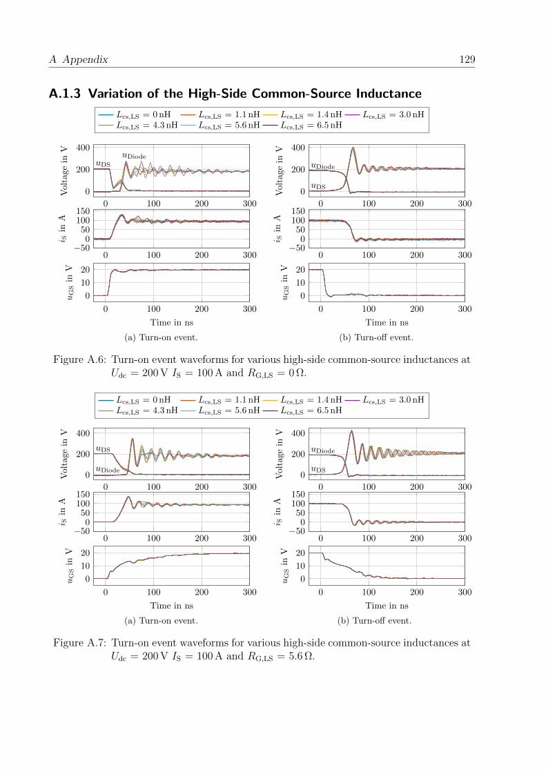
A Appendix 129
A.1.3 Variation of the High-Side Common-Source Inductance
Lcs,LS = 0nH Lcs,LS = 1.1 nH Lcs,LS = 1.4 nH Lcs,LS = 3.0 nHLcs,LS = 4.3 nH Lcs,LS = 5.6 nH Lcs,LS = 6.5 nH
0 100 200 300
0
200
400
Voltagein
V
uDS
uDiode
0 100 200 300−50
050100150
i Sin
A
0 100 200 300
0
10
20
Time in ns
uGSin
V
(a) Turn-on event.
0 100 200 300
0
200
400
Voltagein
V
uDiode
uDS
0 100 200 300−50
050100150
i Sin
A
0 100 200 300
0
10
20
Time in ns
uGSin
V
(b) Turn-off event.
Figure A.6: Turn-on event waveforms for various high-side common-source inductances atUdc = 200 V IS = 100 A and RG,LS = 0 Ω.
Lcs,LS = 0nH Lcs,LS = 1.1 nH Lcs,LS = 1.4 nH Lcs,LS = 3.0 nHLcs,LS = 4.3 nH Lcs,LS = 5.6 nH Lcs,LS = 6.5 nH
0 100 200 300
0
200
400
Voltagein
V
uDS
uDiode
0 100 200 300−50
050100150
i Sin
A
0 100 200 300
0
10
20
Time in ns
uGSin
V
(a) Turn-on event.
0 100 200 300
0
200
400
Voltagein
V
uDiode
uDS
0 100 200 300−50
050100150
i Sin
A
0 100 200 300
0
10
20
Time in ns
uGSin
V
(b) Turn-off event.
Figure A.7: Turn-on event waveforms for various high-side common-source inductances atUdc = 200 V IS = 100 A and RG,LS = 5.6 Ω.
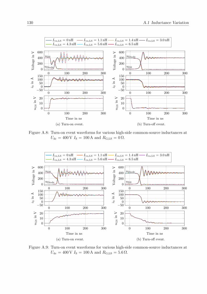
130 A.1 Inductance Variation
Lcs,LS = 0nH Lcs,LS = 1.1 nH Lcs,LS = 1.4 nH Lcs,LS = 3.0 nHLcs,LS = 4.3 nH Lcs,LS = 5.6 nH Lcs,LS = 6.5 nH
0 100 200 3000
200
400
600
Voltagein
V
uDS
uDiode
0 100 200 300−50
050100150
i Sin
A
0 100 200 300
0
10
20
Time in ns
uGSin
V
(a) Turn-on event.
0 100 200 3000
200
400
600
Voltagein
V
uDiode
uDS
0 100 200 300−50
050100150
i Sin
A0 100 200 300
0
10
20
Time in nsuGSin
V
(b) Turn-off event.
Figure A.8: Turn-on event waveforms for various high-side common-source inductances atUdc = 400 V IS = 100 A and RG,LS = 0 Ω.
Lcs,LS = 0nH Lcs,LS = 1.1 nH Lcs,LS = 1.4 nH Lcs,LS = 3.0 nHLcs,LS = 4.3 nH Lcs,LS = 5.6 nH Lcs,LS = 6.5 nH
0 100 200 3000
200
400
600
Voltagein
V
uDS
uDiode
0 100 200 300−50
050100150
i Sin
A
0 100 200 300
0
10
20
Time in ns
uGSin
V
(a) Turn-on event.
0 100 200 3000
200
400
600
Voltagein
V
uDiode
uDS
0 100 200 300−50
050100150
i Sin
A
0 100 200 300
0
10
20
Time in ns
uGSin
V
(b) Turn-off event.
Figure A.9: Turn-on event waveforms for various high-side common-source inductances atUdc = 400 V IS = 100 A and RG,LS = 5.6 Ω.
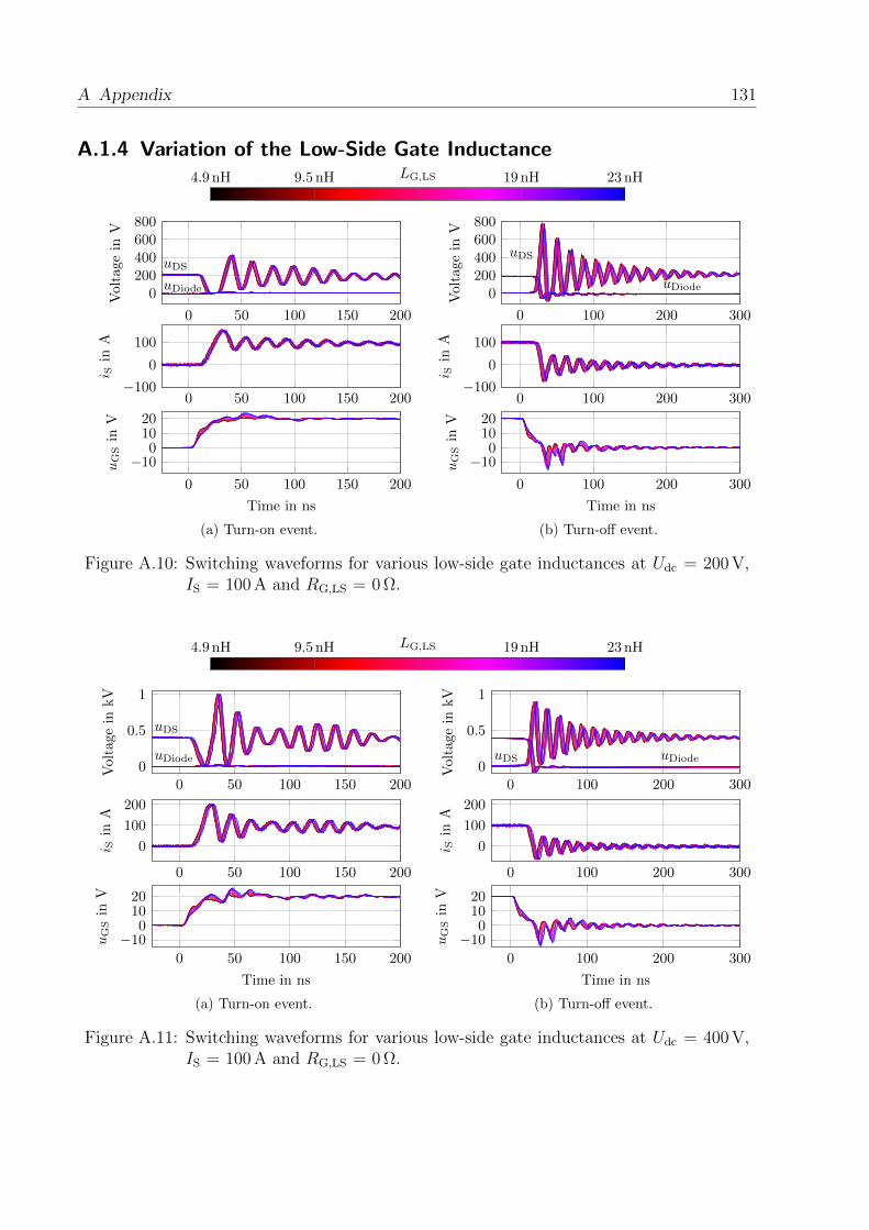
A Appendix 131
A.1.4 Variation of the Low-Side Gate Inductance4.9 nH 9.5 nH LG,LS 19 nH 23 nH
0 50 100 150 200
0200400600800
Voltagein
V
uDS
uDiode
0 50 100 150 200−100
0
100
i Sin
A
0 50 100 150 200
−1001020
Time in ns
uGSin
V
(a) Turn-on event.
0 100 200 300
0200400600800
Voltagein
V
uDiode
uDS
0 100 200 300−100
0
100
i Sin
A
0 100 200 300
−1001020
Time in ns
uGSin
V
(b) Turn-off event.
Figure A.10: Switching waveforms for various low-side gate inductances at Udc = 200 V,IS = 100 A and RG,LS = 0 Ω.
4.9 nH 9.5 nH LG,LS 19 nH 23 nH
0 50 100 150 2000
0.5
1
Voltage
inkV
uDS
uDiode
0 50 100 150 200
0
100
200
i Sin
A
0 50 100 150 200
−1001020
Time in ns
uGSin
V
(a) Turn-on event.
0 100 200 3000
0.5
1
Voltage
inkV
uDiodeuDS
0 100 200 300
0
100
200
i Sin
A
0 100 200 300
−1001020
Time in ns
uGSin
V
(b) Turn-off event.
Figure A.11: Switching waveforms for various low-side gate inductances at Udc = 400 V,IS = 100 A and RG,LS = 0 Ω.
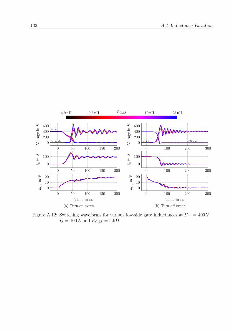
132 A.1 Inductance Variation
4.9 nH 9.5 nH LG,LS 19 nH 23 nH
0 50 100 150 200
0
200
400
600
Voltagein
V
uDS
uDiode
0 50 100 150 200
0
100
i Sin
A
0 50 100 150 200
0
10
20
Time in ns
uGSin
V
(a) Turn-on event.
0 100 200 300
0
200
400
600Voltagein
V
uDiodeuDS
0 100 200 300
0
100
i Sin
A
0 100 200 300
0
10
20
Time in ns
uGSin
V
(b) Turn-off event.
Figure A.12: Switching waveforms for various low-side gate inductances at Udc = 400 V,IS = 100 A and RG,LS = 5.6 Ω.

A Appendix 133
A.1.5 Variation of the High-Side Gate Inductance
7.3 nH 12 nH LG,HS 21 nH 26 nH
0 50 100 150 200
0200400600800
Voltagein
V
uDS
uDiode
0 50 100 150 200−100
0
100
i Sin
A
0 50 100 150 200−10
01020
Time in ns
uGSin
V
(a) Turn-on event.
0 50 100 150 200
0200400600800
Voltagein
V
uDiode
uDS
0 50 100 150 200−100
0
100
i Sin
A
0 50 100 150 200−10
01020
Time in ns
uGSin
V
(b) Turn-off event.
Figure A.13: Turn-on event waveforms for various high-side gate inductances atUdc = 200 V, IS = 100 A and RG,LS = 0 Ω.
7.3 nH 12 nH LG,HS 21 nH 26 nH
0 50 100 150 200
0
200
400
Voltage
inV
uDS
uDiode
0 50 100 150 200−50
050
100150
i Sin
A
0 50 100 150 200
0
10
20
Time in ns
uGSin
V
(a) Turn-on event.
0 50 100 150 200
0
200
400
Voltage
inV
uDiode
uDS
0 50 100 150 200−50
050
100150
i Sin
A
0 50 100 150 200
0
10
20
Time in ns
uGSin
V
(b) Turn-off event.
Figure A.14: Turn-on event waveforms for various high-side gate inductances atUdc = 200 V, IS = 100 A and RG,LS = 5.6 Ω.
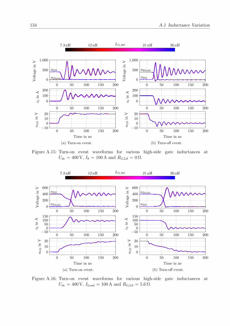
134 A.1 Inductance Variation
7.3 nH 12 nH LG,HS 21 nH 26 nH
0 50 100 150 200
0
500
1,000
Voltagein
V
uDS
uDiode
0 50 100 150 200
0
100
200
i Sin
A
0 50 100 150 200−10
01020
Time in ns
uGSin
V
(a) Turn-on event.
0 50 100 150 200
0
500
1,000
Voltagein
V
uDiode
uDS
0 50 100 150 200
0
100
200
i Sin
A0 50 100 150 200
−1001020
Time in ns
uGSin
V
(b) Turn-off event.
Figure A.15: Turn-on event waveforms for various high-side gate inductances atUdc = 400 V, IS = 100 A and RG,LS = 0 Ω.
7.3 nH 12 nH LG,HS 21 nH 26 nH
0 50 100 150 2000
200
400
600
Voltagein
V
uDS
uDiode
0 50 100 150 200−50
050
100150
i Sin
A
0 50 100 150 200
0
10
20
Time in ns
uGSin
V
(a) Turn-on event.
0 50 100 150 2000
200
400
600
Voltagein
V
uDiode
uDS
0 50 100 150 200−50
050
100150
i Sin
A
0 50 100 150 200
0
10
20
Time in ns
uGSin
V
(b) Turn-off event.
Figure A.16: Turn-on event waveforms for various high-side gate inductances atUdc = 400 V, ILoad = 100 A and RG,LS = 5.6 Ω.
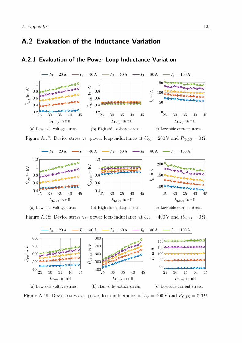
A Appendix 135
A.2 Evaluation of the Inductance Variation
A.2.1 Evaluation of the Power Loop Inductance Variation
IS = 20A IS = 40A IS = 60A IS = 80A IS = 100A
25 30 35 40 450.2
0.4
0.6
0.8
1
LLoop in nH
UDSin
kV
(a) Low-side voltage stress.
25 30 35 40 450.2
0.4
0.6
0.8
1
LLoop in nH
UDiodein
kV
(b) High-side voltage stress.
25 30 35 40 450
50
100
150
LLoop in nH
I Sin
A
(c) Low-side current stress.
Figure A.17: Device stress vs. power loop inductance at Udc = 200 V and RG,LS = 0 Ω.
IS = 20A IS = 40A IS = 60A IS = 80A IS = 100A
25 30 35 40 450.4
0.6
0.8
1
1.2
LLoop in nH
UDSin
kV
(a) Low-side voltage stress.
25 30 35 40 450.4
0.6
0.8
1
1.2
LLoop in nH
UDiodein
kV
(b) High-side voltage stress.
25 30 35 40 45
100
150
200
LLoop in nH
I Sin
A
(c) Low-side current stress.
Figure A.18: Device stress vs. power loop inductance at Udc = 400 V and RG,LS = 0 Ω.
IS = 20A IS = 40A IS = 60A IS = 80A IS = 100A
25 30 35 40 45400
500
600
700
800
LLoop in nH
UDSin
V
(a) Low-side voltage stress.
25 30 35 40 45400
500
600
700
800
LLoop in nH
UDiodein
V
(b) High-side voltage stress.
25 30 35 40 45
60
80
100
120
140
LLoop in nH
I Sin
A
(c) Low-side current stress.
Figure A.19: Device stress vs. power loop inductance at Udc = 400 V and RG,LS = 5.6 Ω.
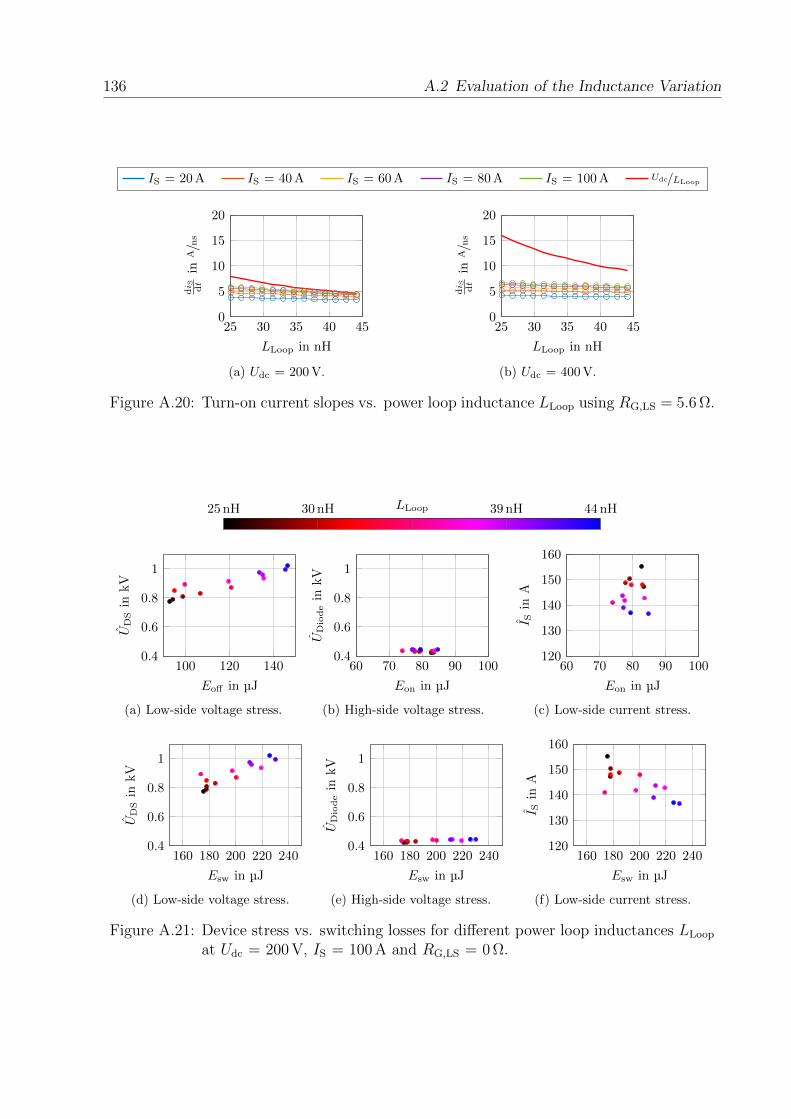
136 A.2 Evaluation of the Inductance Variation
IS = 20A IS = 40A IS = 60A IS = 80A IS = 100A Udc/LLoop
25 30 35 40 450
5
10
15
20
LLoop in nH
di S dtin
A/n
s
(a) Udc = 200 V.
25 30 35 40 450
5
10
15
20
LLoop in nH
di S dtin
A/n
s
(b) Udc = 400 V.
Figure A.20: Turn-on current slopes vs. power loop inductance LLoop using RG,LS = 5.6 Ω.
25 nH 30 nH LLoop 39 nH 44 nH
100 120 1400.4
0.6
0.8
1
Eoff in µJ
UD
Sin
kV
(a) Low-side voltage stress.
60 70 80 90 1000.4
0.6
0.8
1
Eon in µJ
UDiodein
kV
(b) High-side voltage stress.
60 70 80 90 100120
130
140
150
160
Eon in µJ
I Sin
A
(c) Low-side current stress.
160 180 200 220 2400.4
0.6
0.8
1
Esw in µJ
UDSin
kV
(d) Low-side voltage stress.
160 180 200 220 2400.4
0.6
0.8
1
Esw in µJ
UDiodein
kV
(e) High-side voltage stress.
160 180 200 220 240120
130
140
150
160
Esw in µJ
I Sin
A
(f) Low-side current stress.
Figure A.21: Device stress vs. switching losses for different power loop inductances LLoop
at Udc = 200 V, IS = 100 A and RG,LS = 0 Ω.
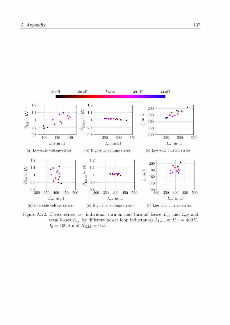
A Appendix 137
25 nH 30 nH LLoop 39 nH 44 nH
100 120 1400.8
0.9
1
1.1
1.2
Eoff in µJ
UD
Sin
kV
(a) Low-side voltage stress.
250 300 3500.8
0.9
1
1.1
1.2
Eon in µJ
UDiodein
kV
(b) High-side voltage stress.
250 300 350120
140
160
180
200
Eon in µJI S
inA
(c) Low-side current stress.
300 350 400 450 5000.8
0.9
1
1.1
1.2
Esw in µJ
UDSin
kV
(d) Low-side voltage stress.
300 350 400 450 5000.8
0.9
1
1.1
1.2
Esw in µJ
UDiodein
kV
(e) High-side voltage stress.
300 350 400 450 500120
140
160
180
200
Esw in µJ
I Sin
A
(f) Low-side current stress.
Figure A.22: Device stress vs. individual turn-on and turn-off losses Eon and Eoff andtotal losses Esw for different power loop inductances LLoop at Udc = 400 V,IS = 100 A and RG,LS = 0 Ω.
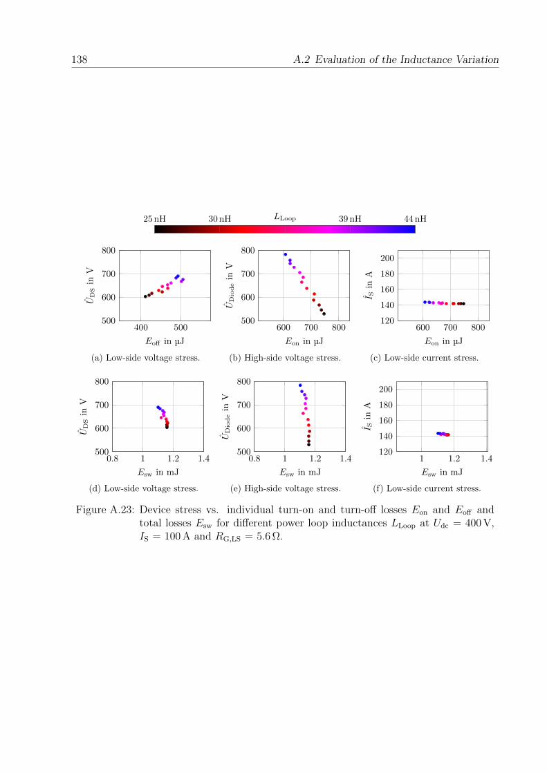
138 A.2 Evaluation of the Inductance Variation
25 nH 30 nH LLoop 39 nH 44 nH
400 500500
600
700
800
Eoff in µJ
UD
Sin
V
(a) Low-side voltage stress.
600 700 800500
600
700
800
Eon in µJ
UDiodein
V
(b) High-side voltage stress.
600 700 800120
140
160
180
200
Eon in µJ
I Sin
A(c) Low-side current stress.
0.8 1 1.2 1.4500
600
700
800
Esw in mJ
UDSin
V
(d) Low-side voltage stress.
0.8 1 1.2 1.4500
600
700
800
Esw in mJ
UDiodein
V
(e) High-side voltage stress.
1 1.2 1.4120
140
160
180
200
Esw in mJ
I Sin
A
(f) Low-side current stress.
Figure A.23: Device stress vs. individual turn-on and turn-off losses Eon and Eoff andtotal losses Esw for different power loop inductances LLoop at Udc = 400 V,IS = 100 A and RG,LS = 5.6 Ω.
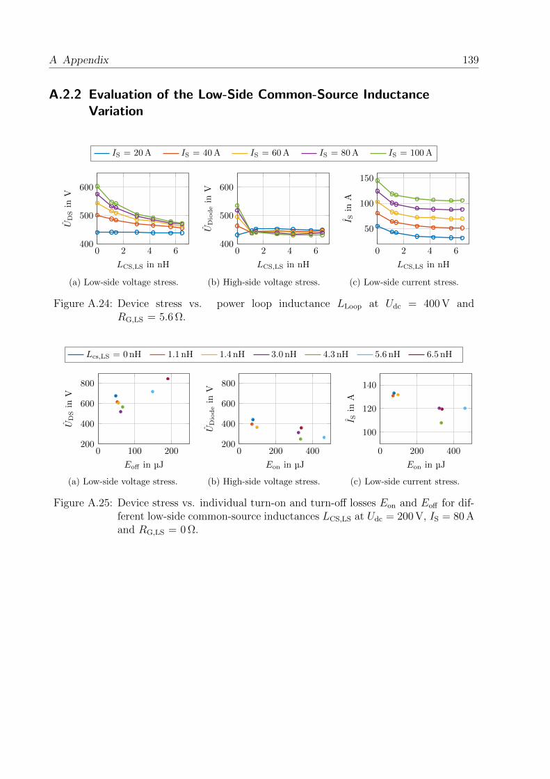
A Appendix 139
A.2.2 Evaluation of the Low-Side Common-Source InductanceVariation
IS = 20A IS = 40A IS = 60A IS = 80A IS = 100A
0 2 4 6400
500
600
LCS,LS in nH
UDSin
V
(a) Low-side voltage stress.
0 2 4 6400
500
600
LCS,LS in nH
UDiodein
V
(b) High-side voltage stress.
0 2 4 6
50
100
150
LCS,LS in nH
I Sin
A
(c) Low-side current stress.
Figure A.24: Device stress vs. power loop inductance LLoop at Udc = 400 V andRG,LS = 5.6 Ω.
Lcs,LS = 0nH 1.1 nH 1.4 nH 3.0 nH 4.3 nH 5.6 nH 6.5 nH
0 100 200200
400
600
800
Eoff in µJ
UD
Sin
V
(a) Low-side voltage stress.
0 200 400200
400
600
800
Eon in µJ
UDiodein
V
(b) High-side voltage stress.
0 200 400
100
120
140
Eon in µJ
I Sin
A
(c) Low-side current stress.
Figure A.25: Device stress vs. individual turn-on and turn-off losses Eon and Eoff for dif-ferent low-side common-source inductances LCS,LS at Udc = 200 V, IS = 80 Aand RG,LS = 0 Ω.
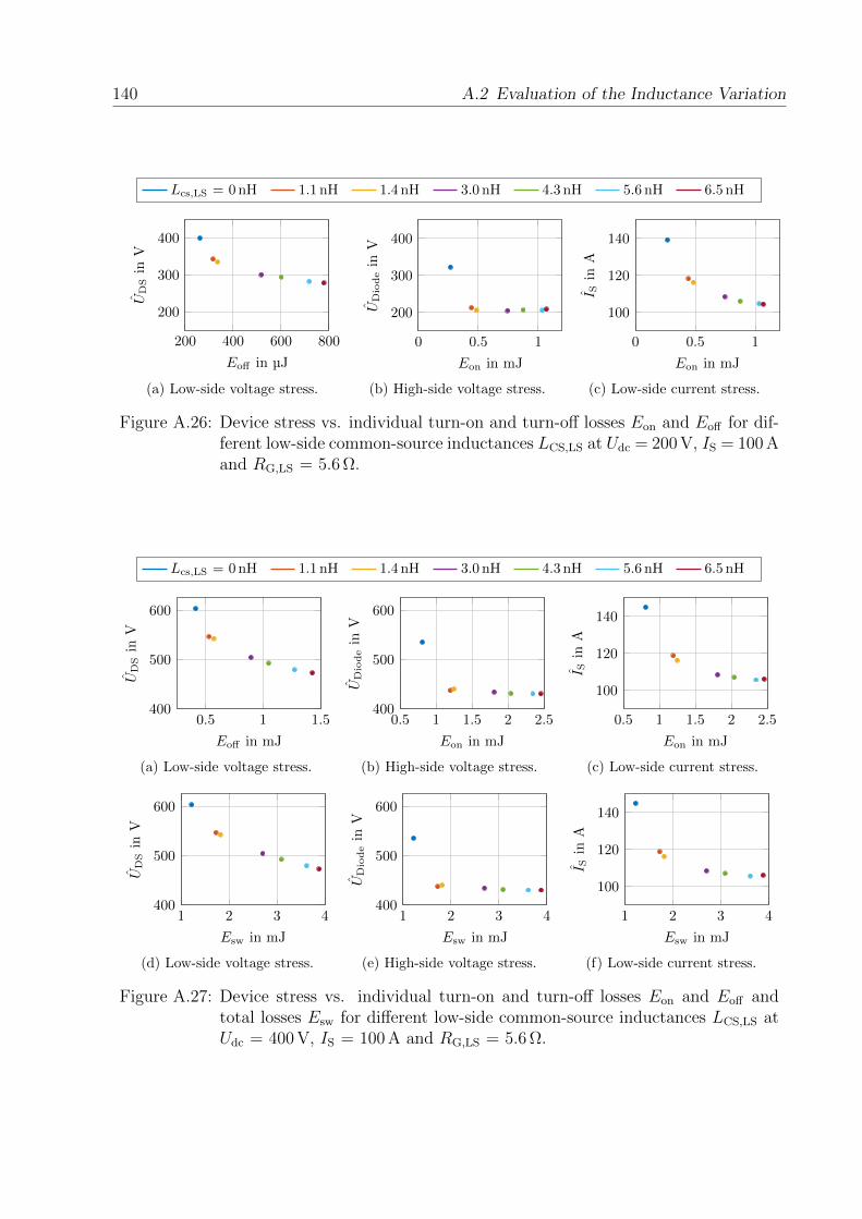
140 A.2 Evaluation of the Inductance Variation
Lcs,LS = 0nH 1.1 nH 1.4 nH 3.0 nH 4.3 nH 5.6 nH 6.5 nH
200 400 600 800
200
300
400
Eoff in µJ
UD
Sin
V
(a) Low-side voltage stress.
0 0.5 1
200
300
400
Eon in mJUDiodein
V
(b) High-side voltage stress.
0 0.5 1
100
120
140
Eon in mJ
I Sin
A
(c) Low-side current stress.
Figure A.26: Device stress vs. individual turn-on and turn-off losses Eon and Eoff for dif-ferent low-side common-source inductances LCS,LS at Udc = 200 V, IS = 100 Aand RG,LS = 5.6 Ω.
Lcs,LS = 0nH 1.1 nH 1.4 nH 3.0 nH 4.3 nH 5.6 nH 6.5 nH
0.5 1 1.5400
500
600
Eoff in mJ
UD
Sin
V
(a) Low-side voltage stress.
0.5 1 1.5 2 2.5400
500
600
Eon in mJ
UDiodein
V
(b) High-side voltage stress.
0.5 1 1.5 2 2.5
100
120
140
Eon in mJ
I Sin
A
(c) Low-side current stress.
1 2 3 4400
500
600
Esw in mJ
UDSin
V
(d) Low-side voltage stress.
1 2 3 4400
500
600
Esw in mJ
UDiodein
V
(e) High-side voltage stress.
1 2 3 4
100
120
140
Esw in mJ
I Sin
A
(f) Low-side current stress.
Figure A.27: Device stress vs. individual turn-on and turn-off losses Eon and Eoff andtotal losses Esw for different low-side common-source inductances LCS,LS atUdc = 400 V, IS = 100 A and RG,LS = 5.6 Ω.
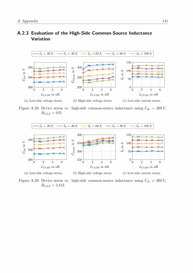
A Appendix 141
A.2.3 Evaluation of the High-Side Common-Source InductanceVariation
IS = 20A IS = 40A IS = 60A IS = 80A IS = 100A
0 2 4 6200
300
400
LCS,HS in nH
UDSin
V
(a) Low-side voltage stress.
0 2 4 6200
300
400
LCS,HS in nH
UDiodein
V
(b) High-side voltage stress.
0 2 4 60
50
100
150
LCS,HS in nH
I Sin
A
(c) Low-side current stress.
Figure A.28: Device stress vs. high-side common-source inductance using Udc = 200 V,RG,LS = 0 Ω.
IS = 20A IS = 40A IS = 60A IS = 80A IS = 100A
0 2 4 6200
300
400
LCS,HS in nH
UDSin
V
(a) Low-side voltage stress.
0 2 4 6250
300
350
400
LCS,HS in nH
UDiodein
V
(b) High-side voltage stress.
0 2 4 60
50
100
150
LCS,HS in nH
I Sin
A
(c) Low-side current stress.
Figure A.29: Device stress vs. high-side common-source inductance using Udc = 200 V,RG,LS = 5.6 Ω.
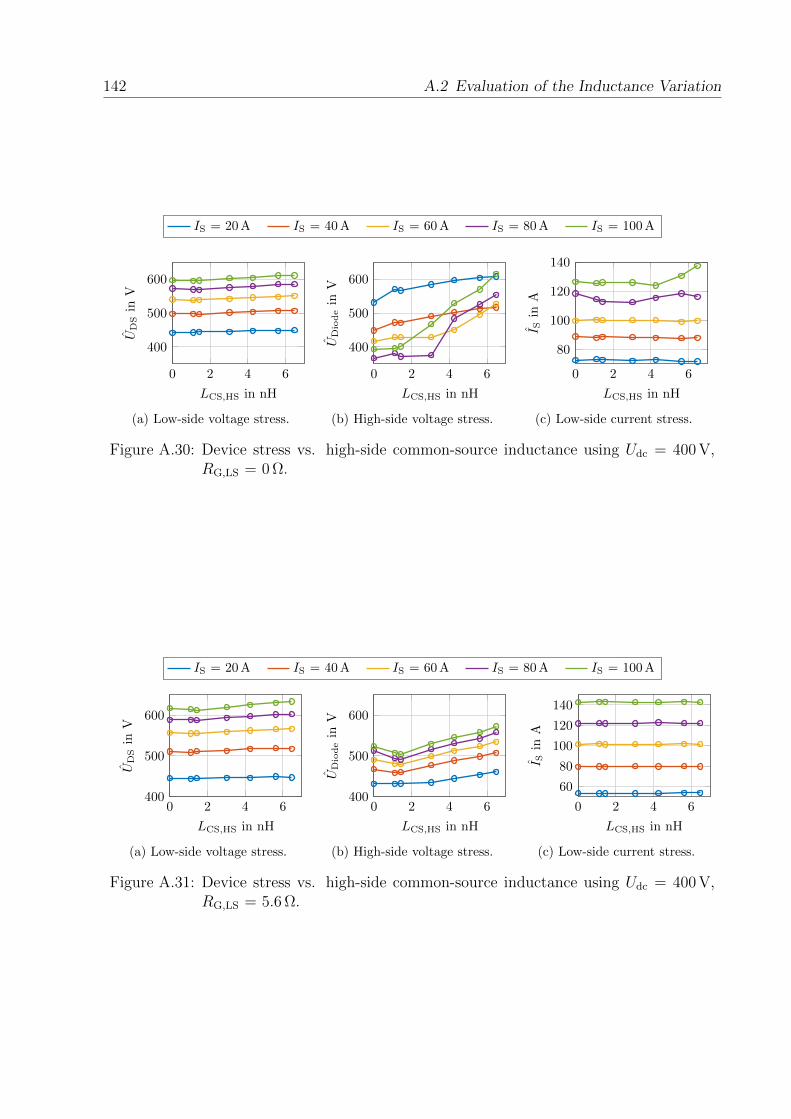
142 A.2 Evaluation of the Inductance Variation
IS = 20A IS = 40A IS = 60A IS = 80A IS = 100A
0 2 4 6
400
500
600
LCS,HS in nH
UDSin
V
(a) Low-side voltage stress.
0 2 4 6
400
500
600
LCS,HS in nH
UDiodein
V
(b) High-side voltage stress.
0 2 4 6
80
100
120
140
LCS,HS in nH
I Sin
A
(c) Low-side current stress.
Figure A.30: Device stress vs. high-side common-source inductance using Udc = 400 V,RG,LS = 0 Ω.
IS = 20A IS = 40A IS = 60A IS = 80A IS = 100A
0 2 4 6400
500
600
LCS,HS in nH
UDSin
V
(a) Low-side voltage stress.
0 2 4 6400
500
600
LCS,HS in nH
UDiodein
V
(b) High-side voltage stress.
0 2 4 6
60
80
100
120
140
LCS,HS in nH
I Sin
A
(c) Low-side current stress.
Figure A.31: Device stress vs. high-side common-source inductance using Udc = 400 V,RG,LS = 5.6 Ω.
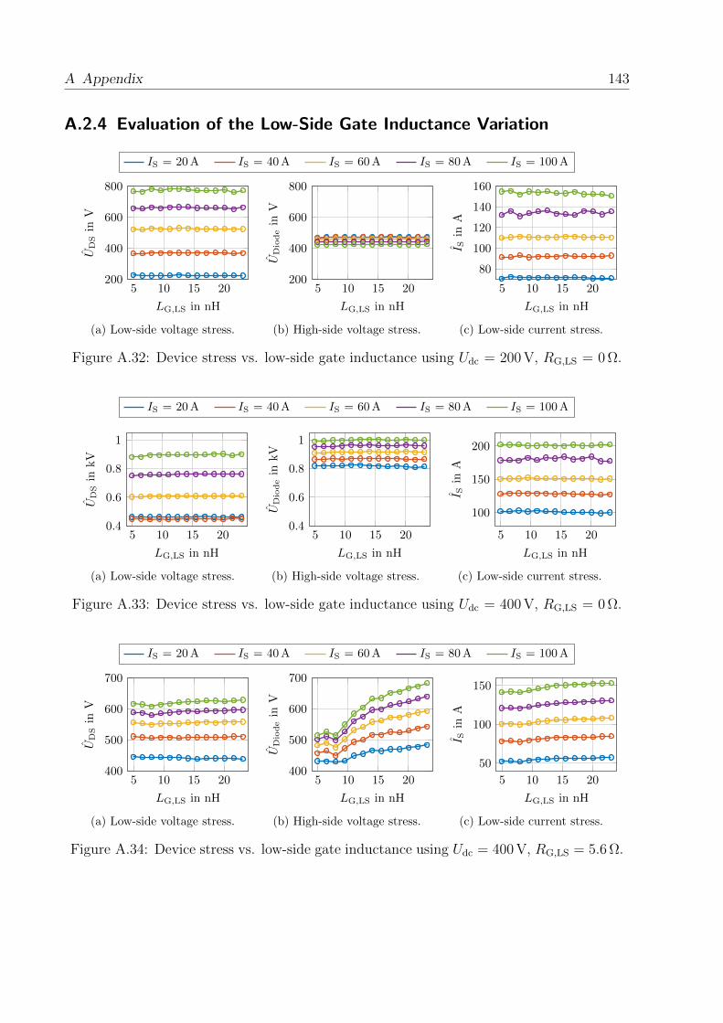
A Appendix 143
A.2.4 Evaluation of the Low-Side Gate Inductance Variation
IS = 20A IS = 40A IS = 60A IS = 80A IS = 100A
5 10 15 20200
400
600
800
LG,LS in nH
UDSin
V
(a) Low-side voltage stress.
5 10 15 20200
400
600
800
LG,LS in nH
UDiodein
V
(b) High-side voltage stress.
5 10 15 20
80
100
120
140
160
LG,LS in nH
I Sin
A
(c) Low-side current stress.
Figure A.32: Device stress vs. low-side gate inductance using Udc = 200 V, RG,LS = 0 Ω.
IS = 20A IS = 40A IS = 60A IS = 80A IS = 100A
5 10 15 200.4
0.6
0.8
1
LG,LS in nH
UDSin
kV
(a) Low-side voltage stress.
5 10 15 200.4
0.6
0.8
1
LG,LS in nH
UDiodein
kV
(b) High-side voltage stress.
5 10 15 20
100
150
200
LG,LS in nH
I Sin
A
(c) Low-side current stress.
Figure A.33: Device stress vs. low-side gate inductance using Udc = 400 V, RG,LS = 0 Ω.
IS = 20A IS = 40A IS = 60A IS = 80A IS = 100A
5 10 15 20400
500
600
700
LG,LS in nH
UDSin
V
(a) Low-side voltage stress.
5 10 15 20400
500
600
700
LG,LS in nH
UDiodein
V
(b) High-side voltage stress.
5 10 15 20
50
100
150
LG,LS in nH
I Sin
A
(c) Low-side current stress.
Figure A.34: Device stress vs. low-side gate inductance using Udc = 400 V, RG,LS = 5.6 Ω.
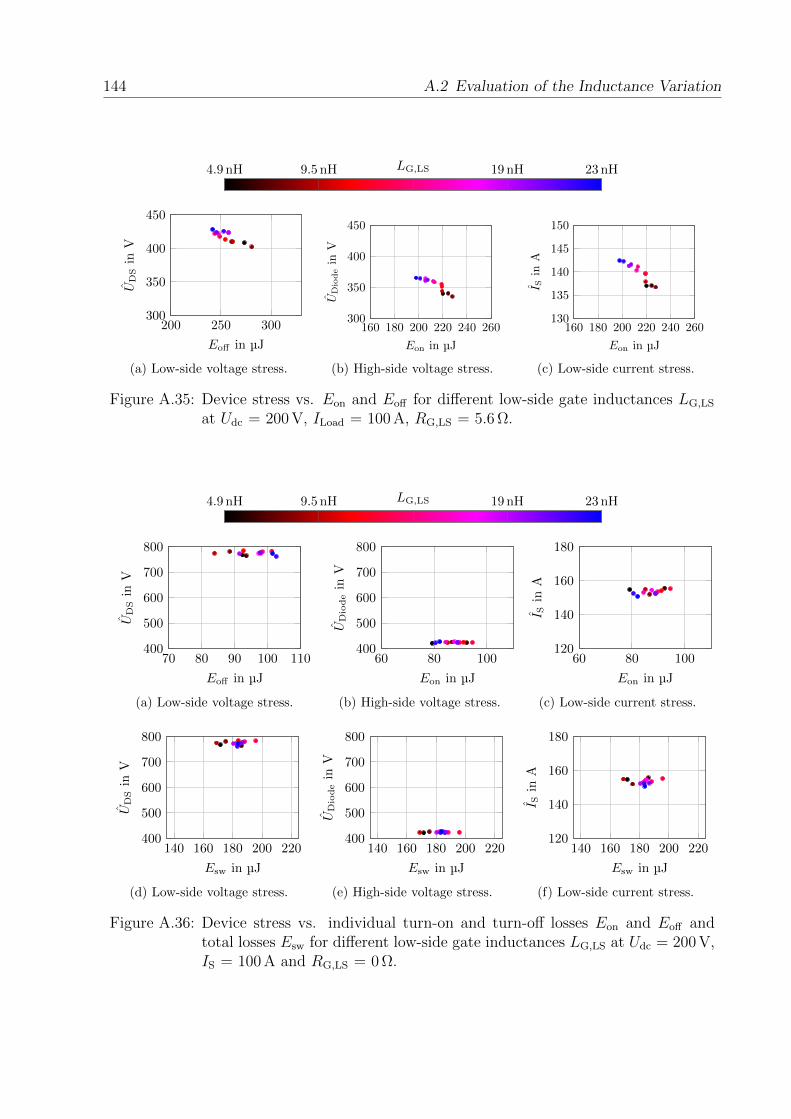
144 A.2 Evaluation of the Inductance Variation
4.9 nH 9.5 nH LG,LS 19 nH 23 nH
200 250 300300
350
400
450
Eoff in µJ
UD
Sin
V
(a) Low-side voltage stress.
160 180 200 220 240 260300
350
400
450
Eon in µJUDiodein
V
(b) High-side voltage stress.
160 180 200 220 240 260130
135
140
145
150
Eon in µJ
I Sin
A
(c) Low-side current stress.
Figure A.35: Device stress vs. Eon and Eoff for different low-side gate inductances LG,LS
at Udc = 200 V, ILoad = 100 A, RG,LS = 5.6 Ω.
4.9 nH 9.5 nH LG,LS 19 nH 23 nH
70 80 90 100 110400
500
600
700
800
Eoff in µJ
UD
Sin
V
(a) Low-side voltage stress.
60 80 100400
500
600
700
800
Eon in µJ
UDiodein
V
(b) High-side voltage stress.
60 80 100120
140
160
180
Eon in µJ
I Sin
A
(c) Low-side current stress.
140 160 180 200 220400
500
600
700
800
Esw in µJ
UDSin
V
(d) Low-side voltage stress.
140 160 180 200 220400
500
600
700
800
Esw in µJ
UDiodein
V
(e) High-side voltage stress.
140 160 180 200 220120
140
160
180
Esw in µJ
I Sin
A
(f) Low-side current stress.
Figure A.36: Device stress vs. individual turn-on and turn-off losses Eon and Eoff andtotal losses Esw for different low-side gate inductances LG,LS at Udc = 200 V,IS = 100 A and RG,LS = 0 Ω.
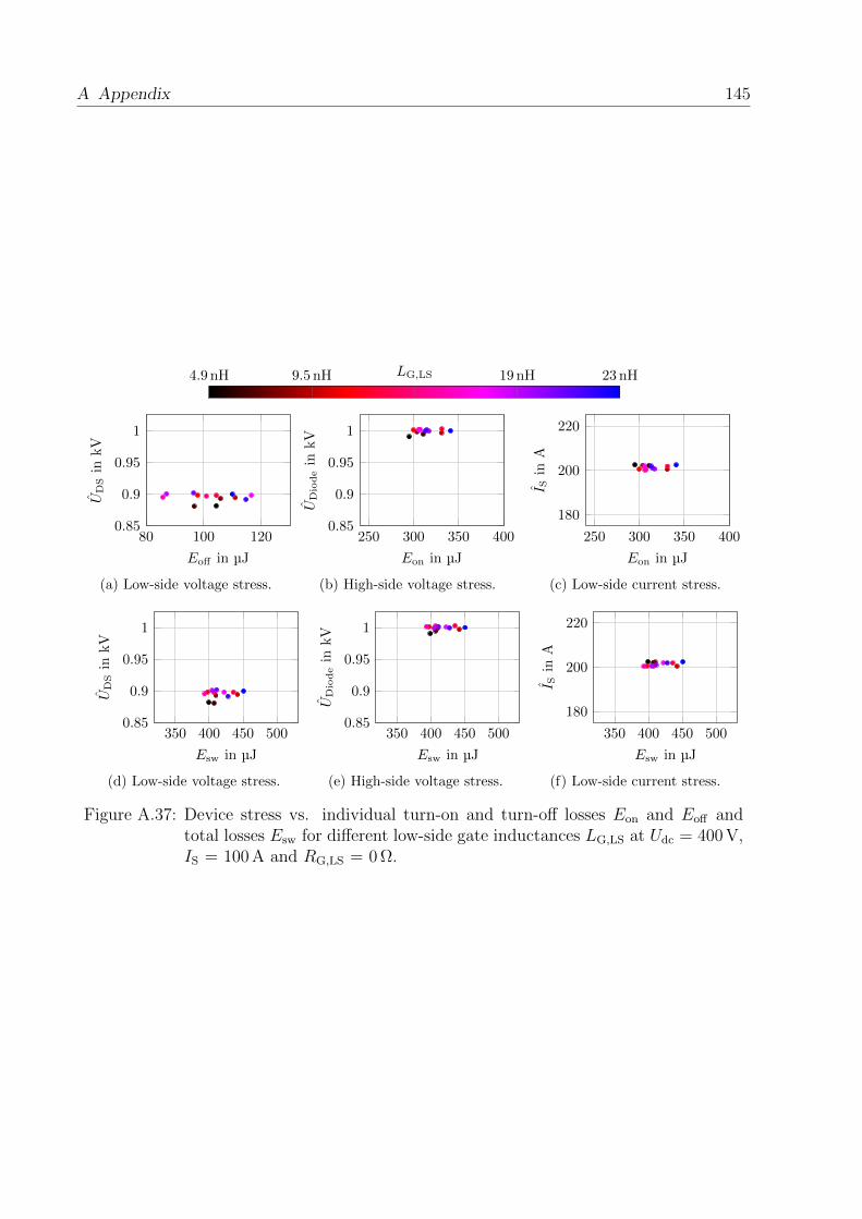
A Appendix 145
4.9 nH 9.5 nH LG,LS 19 nH 23 nH
80 100 1200.85
0.9
0.95
1
Eoff in µJ
UD
Sin
kV
(a) Low-side voltage stress.
250 300 350 4000.85
0.9
0.95
1
Eon in µJ
UDiodein
kV
(b) High-side voltage stress.
250 300 350 400
180
200
220
Eon in µJI S
inA
(c) Low-side current stress.
350 400 450 5000.85
0.9
0.95
1
Esw in µJ
UDSin
kV
(d) Low-side voltage stress.
350 400 450 5000.85
0.9
0.95
1
Esw in µJ
UDiodein
kV
(e) High-side voltage stress.
350 400 450 500
180
200
220
Esw in µJ
I Sin
A
(f) Low-side current stress.
Figure A.37: Device stress vs. individual turn-on and turn-off losses Eon and Eoff andtotal losses Esw for different low-side gate inductances LG,LS at Udc = 400 V,IS = 100 A and RG,LS = 0 Ω.
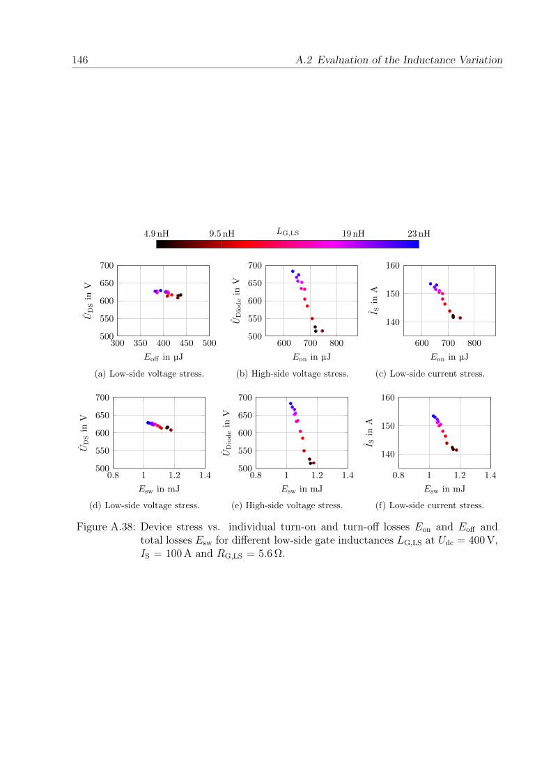
146 A.2 Evaluation of the Inductance Variation
4.9 nH 9.5 nH LG,LS 19 nH 23 nH
300 350 400 450 500500
550
600
650
700
Eoff in µJ
UD
Sin
V
(a) Low-side voltage stress.
600 700 800500
550
600
650
700
Eon in µJ
UDiodein
V
(b) High-side voltage stress.
600 700 800
140
150
160
Eon in µJ
I Sin
A(c) Low-side current stress.
0.8 1 1.2 1.4500
550
600
650
700
Esw in mJ
UDSin
V
(d) Low-side voltage stress.
0.8 1 1.2 1.4500
550
600
650
700
Esw in mJ
UDiodein
V
(e) High-side voltage stress.
0.8 1 1.2 1.4
140
150
160
Esw in mJ
I Sin
A
(f) Low-side current stress.
Figure A.38: Device stress vs. individual turn-on and turn-off losses Eon and Eoff andtotal losses Esw for different low-side gate inductances LG,LS at Udc = 400 V,IS = 100 A and RG,LS = 5.6 Ω.

A Appendix 147
A.2.5 Evaluation of the High-Side Gate Inductance Variation
IS = 20A IS = 40A IS = 60A IS = 80A IS = 100A
5 10 15 20200
400
600
800
LG,HS in nH
UDSin
V
(a) Low-side voltage stress.
5 10 15 20200
400
600
800
LG,HS in nH
UDiodein
V
(b) High-side voltage stress.
5 10 15 20
80
100
120
140
160
LG,HS in nH
I Sin
A
(c) Low-side current stress.
Figure A.39: Device stress vs. high-side gate inductance using Udc = 200 V, RG,LS = 0 Ω.
IS = 20A IS = 40A IS = 60A IS = 80A IS = 100A
5 10 15 20
250
300
350
400
LG,HS in nH
UDSin
V
(a) Low-side voltage stress.
5 10 15 20
250
300
350
400
LG,HS in nH
UDiodein
V
(b) High-side voltage stress.
5 10 15 2040
60
80
100
120
140
LG,HS in nH
I Sin
A
(c) Low-side current stress.
Figure A.40: Device stress vs. high-side gate inductance using Udc = 200 V, RG,LS = 5.6 Ω.
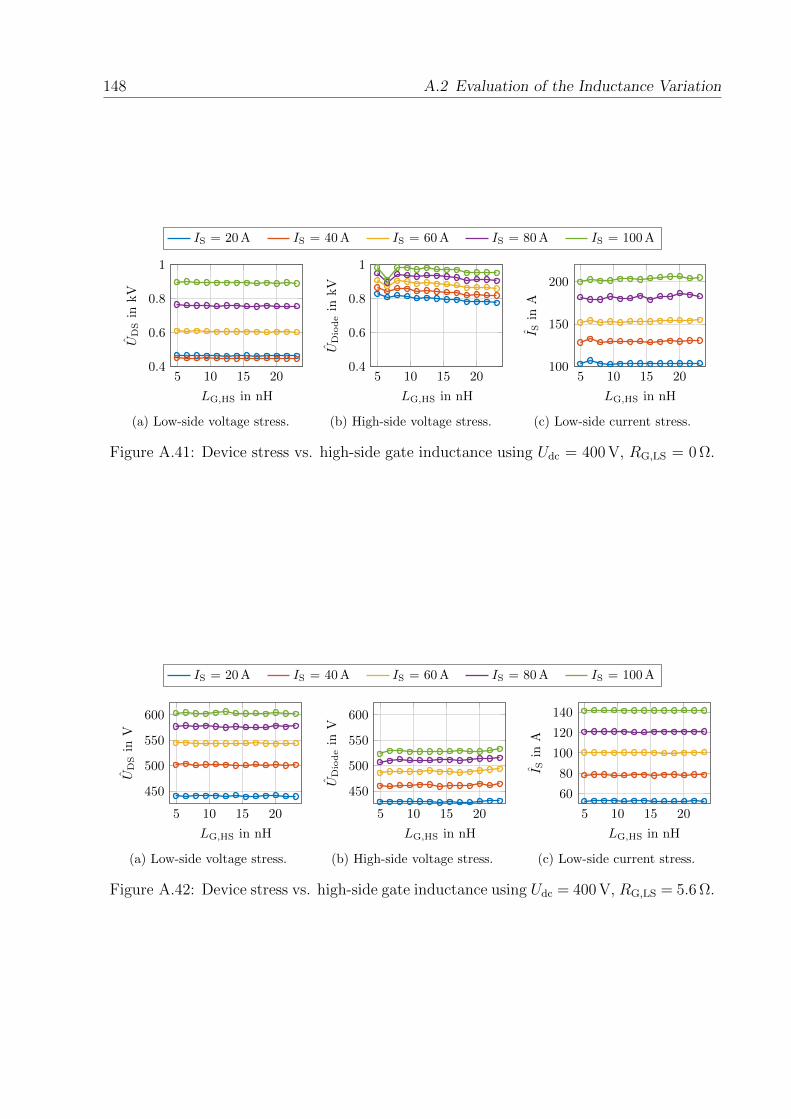
148 A.2 Evaluation of the Inductance Variation
IS = 20A IS = 40A IS = 60A IS = 80A IS = 100A
5 10 15 200.4
0.6
0.8
1
LG,HS in nH
UDSin
kV
(a) Low-side voltage stress.
5 10 15 200.4
0.6
0.8
1
LG,HS in nH
UDiodein
kV
(b) High-side voltage stress.
5 10 15 20100
150
200
LG,HS in nH
I Sin
A
(c) Low-side current stress.
Figure A.41: Device stress vs. high-side gate inductance using Udc = 400 V, RG,LS = 0 Ω.
IS = 20A IS = 40A IS = 60A IS = 80A IS = 100A
5 10 15 20
450
500
550
600
LG,HS in nH
UDSin
V
(a) Low-side voltage stress.
5 10 15 20
450
500
550
600
LG,HS in nH
UDiodein
V
(b) High-side voltage stress.
5 10 15 20
60
80
100
120
140
LG,HS in nH
I Sin
A
(c) Low-side current stress.
Figure A.42: Device stress vs. high-side gate inductance using Udc = 400 V, RG,LS = 5.6 Ω.

A Appendix 149
A.3 Active Gate Driver
A.3.1 Power-On Protection Circuit
UccR1
R2R3
Enable signal
p-channel MOSFET
Stage-wise supply
n-channel MOSFET
Figure A.43: Stage-wise power-on protection circuit.
A.3.2 Investigated Components for the SiC Driver Stage
Table A.1: Investigated push-pull MOSFETs for the SiC driver stage
Type Manufacturer Identifier
n-channel Infineon BSD316SNn-channel Infineon BSS306Nn-channel Infineon BSS316Nn-channel Texas Instruments CSD87502Q2n-channel Diodes Inc. DMN3035LWNn-channel Diodes Inc. DMT3020LFDB-7n-channel Zetex ZXMN3A01Fp-channel Infineon BSD314SPEp-channel Infineon BSS308PEp-channel Infineon BSS314PEp-channel Infineon BSZ180P03NS3Ep-channel On Semiconductor CPH3360p-channel On Semiconductor FDC365Pp-channel On Semiconductor MCH3375p-channel On Semiconductor MCH6664
Table A.2: Investigated MOSFET drivers for the SiC driver stage
Type Manufacturer Identifier
dual low-side Texas Instruments UCC2752xdual low-side On Semiconductor FAN322xsingle low-side IXYS IXDx609single low-side Microchip MIC4421

150 A.3 Active Gate Driver
A.3.3 IGBT Optimized Results
Udc = 200V (reference) Udc = 200V (stage-wise)Udc = 400V (reference) Udc = 400V (stage-wise)
0 100 200 3000
20
40
IE in A
Eonin
mJ
(a) Turn-on losses at ϑj = 35 C.
0 100 200 3000
20
40
IE in A
Eonin
mJ
(b) Turn-on losses at ϑj = 125 C.
0 100 200 3000
10
20
30
IE in A
Eoffin
mJ
(c) Turn-off losses at ϑj = 75 C.
0 100 200 3000
10
20
30
IE in A
Eoffin
mJ
(d) Turn-off losses at ϑj = 125 C.
Figure A.44: Comparison of reference losses to optimized losses at equal device stress.
Table A.3: Loss energy improvements of the investigated operating points
ϑj Udc
IE100 A 200 A 300 A
eon eoff eon eoff eon eoff
35 C200 V 91 % 64 % 86 % 72 % 83 % 69 %400 V 102 % 54 % 96 % 68 % 90 % 74 %
75 C200 V 85 % 63 % 90 % 68 % 84 % 63 %400 V 100 % 57 % 94 % 62 % 91 % 70 %
125 C200 V 94 % 68 % 89 % 73 % 87 % 76 %400 V 105 % 71 % 101 % 74 % 95 % 73 %
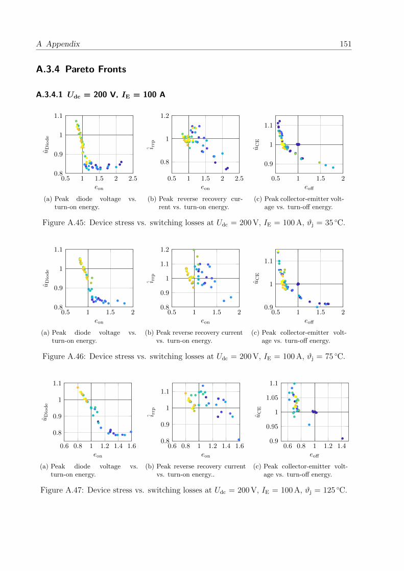
A Appendix 151
A.3.4 Pareto Fronts
A.3.4.1 Udc = 200 V, IE = 100 A
0.5 1 1.5 2 2.50.8
0.9
1
1.1
eon
uDiode
(a) Peak diode voltage vs.turn-on energy.
0.5 1 1.5 2 2.5
0.8
1
1.2
eon
i rrp
(b) Peak reverse recovery cur-rent vs. turn-on energy.
0.5 1 1.5 2
0.9
1
1.1
eoff
uC
E
(c) Peak collector-emitter volt-age vs. turn-off energy.
Figure A.45: Device stress vs. switching losses at Udc = 200 V, IE = 100 A, ϑj = 35 C.
0.5 1 1.5 20.8
0.9
1
1.1
eon
uDiode
(a) Peak diode voltage vs.turn-on energy.
0.5 1 1.5 20.8
0.9
1
1.1
1.2
eon
i rrp
(b) Peak reverse recovery currentvs. turn-on energy.
0.5 1 1.5 20.9
1
1.1
eoff
uC
E
(c) Peak collector-emitter volt-age vs. turn-off energy.
Figure A.46: Device stress vs. switching losses at Udc = 200 V, IE = 100 A, ϑj = 75 C.
0.6 0.8 1 1.2 1.4 1.6
0.8
0.9
1
1.1
eon
uDiode
(a) Peak diode voltage vs.turn-on energy.
0.6 0.8 1 1.2 1.4 1.60.8
0.9
1
1.1
eon
i rrp
(b) Peak reverse recovery currentvs. turn-on energy..
0.6 0.8 1 1.2 1.40.9
0.95
1
1.05
1.1
eoff
uC
E
(c) Peak collector-emitter volt-age vs. turn-off energy.
Figure A.47: Device stress vs. switching losses at Udc = 200 V, IE = 100 A, ϑj = 125 C.
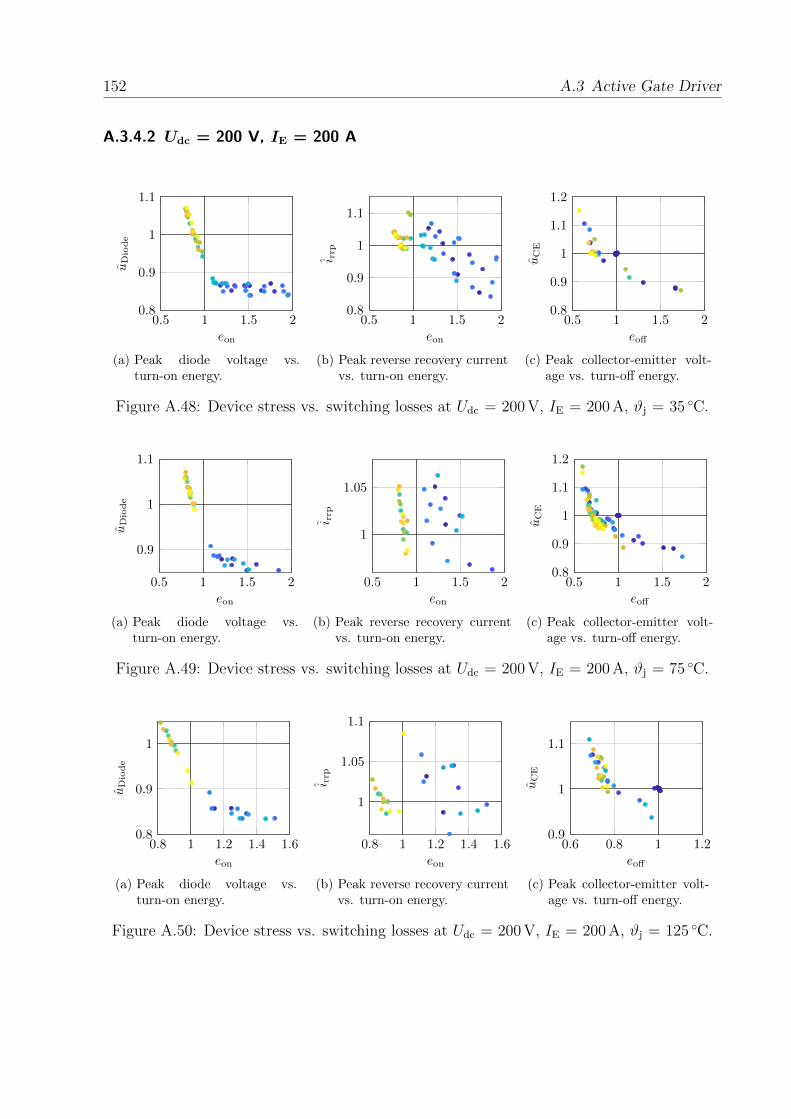
152 A.3 Active Gate Driver
A.3.4.2 Udc = 200 V, IE = 200 A
0.5 1 1.5 20.8
0.9
1
1.1
eon
uDiode
(a) Peak diode voltage vs.turn-on energy.
0.5 1 1.5 20.8
0.9
1
1.1
eoni rrp
(b) Peak reverse recovery currentvs. turn-on energy.
0.5 1 1.5 20.8
0.9
1
1.1
1.2
eoff
uC
E
(c) Peak collector-emitter volt-age vs. turn-off energy.
Figure A.48: Device stress vs. switching losses at Udc = 200 V, IE = 200 A, ϑj = 35 C.
0.5 1 1.5 2
0.9
1
1.1
eon
uDiode
(a) Peak diode voltage vs.turn-on energy.
0.5 1 1.5 2
1
1.05
eon
i rrp
(b) Peak reverse recovery currentvs. turn-on energy.
0.5 1 1.5 20.8
0.9
1
1.1
1.2
eoff
uC
E
(c) Peak collector-emitter volt-age vs. turn-off energy.
Figure A.49: Device stress vs. switching losses at Udc = 200 V, IE = 200 A, ϑj = 75 C.
0.8 1 1.2 1.4 1.60.8
0.9
1
eon
uDiode
(a) Peak diode voltage vs.turn-on energy.
0.8 1 1.2 1.4 1.6
1
1.05
1.1
eon
i rrp
(b) Peak reverse recovery currentvs. turn-on energy.
0.6 0.8 1 1.20.9
1
1.1
eoff
uC
E
(c) Peak collector-emitter volt-age vs. turn-off energy.
Figure A.50: Device stress vs. switching losses at Udc = 200 V, IE = 200 A, ϑj = 125 C.
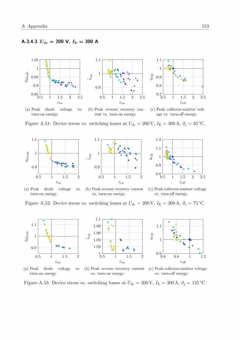
A Appendix 153
A.3.4.3 Udc = 200 V, IE = 300 A
0.5 1 1.5 2 2.50.85
0.9
0.95
1
1.05
eon
uDiode
(a) Peak diode voltage vs.turn-on energy.
0.5 1 1.5 2 2.5
0.9
1
1.1
eon
i rrp
(b) Peak reverse recovery cur-rent vs. turn-on energy.
0.5 1 1.5 2 2.50.7
0.8
0.9
1
1.1
eoff
uC
E
(c) Peak collector-emitter volt-age vs. turn-off energy.
Figure A.51: Device stress vs. switching losses at Udc = 200 V, IE = 300 A, ϑj = 35 C.
0.5 1 1.5 2
0.9
1
1.1
eon
uDiode
(a) Peak diode voltage vs.turn-on energy.
0.5 1 1.5 2
0.9
1
1.1
eon
i rrp
(b) Peak reverse recovery currentvs. turn-on energy.
0.5 1 1.5 2 2.50.8
0.9
1
1.1
1.2
eoff
uC
E
(c) Peak collector-emitter voltagevs. turn-off energy.
Figure A.52: Device stress vs. switching losses at Udc = 200 V, IE = 300 A, ϑj = 75 C.
0.5 1 1.5 2
0.9
1
1.1
eon
uDiode
(a) Peak diode voltage vs.turn-on energy.
0.5 1 1.5 21
1.02
1.04
1.06
1.08
1.1
eon
i rrp
(b) Peak reverse recovery currentvs. turn-on energy.
0.6 0.8 1 1.20.9
1
1.1
eoff
uC
E
(c) Peak collector-emitter voltagevs. turn-off energy.
Figure A.53: Device stress vs. switching losses at Udc = 200 V, IE = 300 A, ϑj = 125 C.
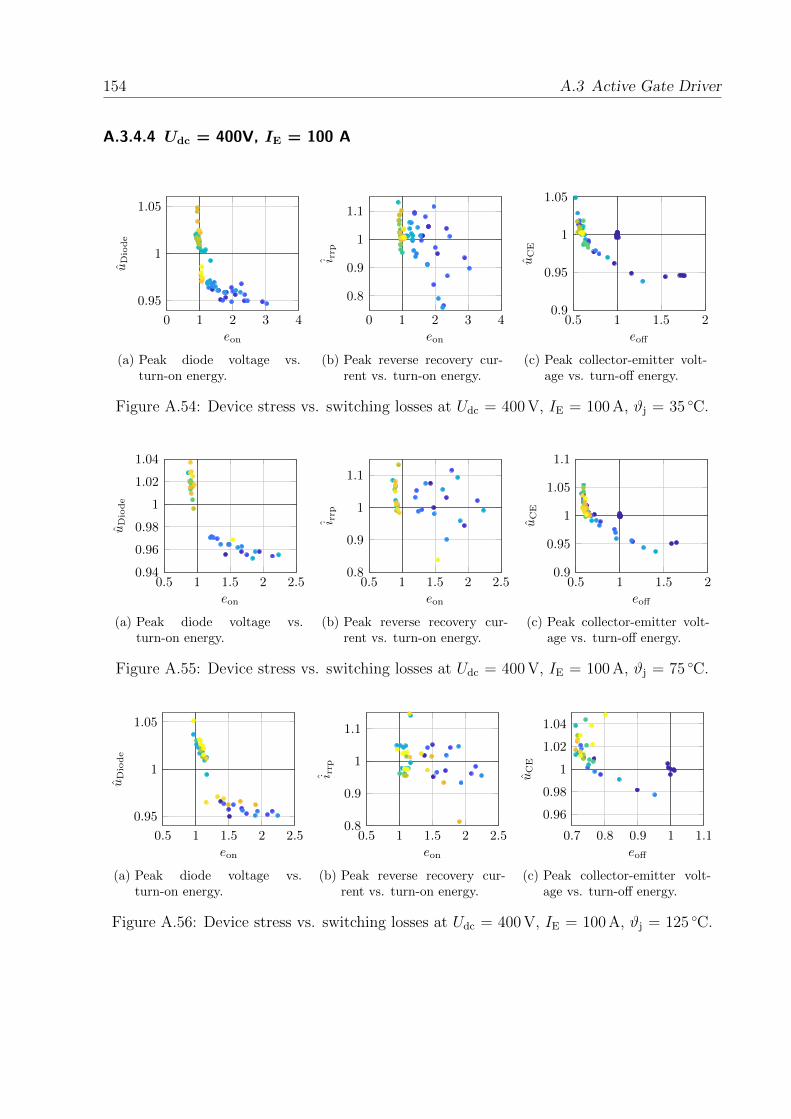
154 A.3 Active Gate Driver
A.3.4.4 Udc = 400V, IE = 100 A
0 1 2 3 4
0.95
1
1.05
eon
uDiode
(a) Peak diode voltage vs.turn-on energy.
0 1 2 3 4
0.8
0.9
1
1.1
eoni rrp
(b) Peak reverse recovery cur-rent vs. turn-on energy.
0.5 1 1.5 20.9
0.95
1
1.05
eoff
uC
E
(c) Peak collector-emitter volt-age vs. turn-off energy.
Figure A.54: Device stress vs. switching losses at Udc = 400 V, IE = 100 A, ϑj = 35 C.
0.5 1 1.5 2 2.50.94
0.96
0.98
1
1.02
1.04
eon
uDiode
(a) Peak diode voltage vs.turn-on energy.
0.5 1 1.5 2 2.50.8
0.9
1
1.1
eon
i rrp
(b) Peak reverse recovery cur-rent vs. turn-on energy.
0.5 1 1.5 20.9
0.95
1
1.05
1.1
eoff
uC
E
(c) Peak collector-emitter volt-age vs. turn-off energy.
Figure A.55: Device stress vs. switching losses at Udc = 400 V, IE = 100 A, ϑj = 75 C.
0.5 1 1.5 2 2.5
0.95
1
1.05
eon
uDiode
(a) Peak diode voltage vs.turn-on energy.
0.5 1 1.5 2 2.50.8
0.9
1
1.1
eon
i rrp
(b) Peak reverse recovery cur-rent vs. turn-on energy.
0.7 0.8 0.9 1 1.1
0.96
0.98
1
1.02
1.04
eoff
uC
E
(c) Peak collector-emitter volt-age vs. turn-off energy.
Figure A.56: Device stress vs. switching losses at Udc = 400 V, IE = 100 A, ϑj = 125 C.
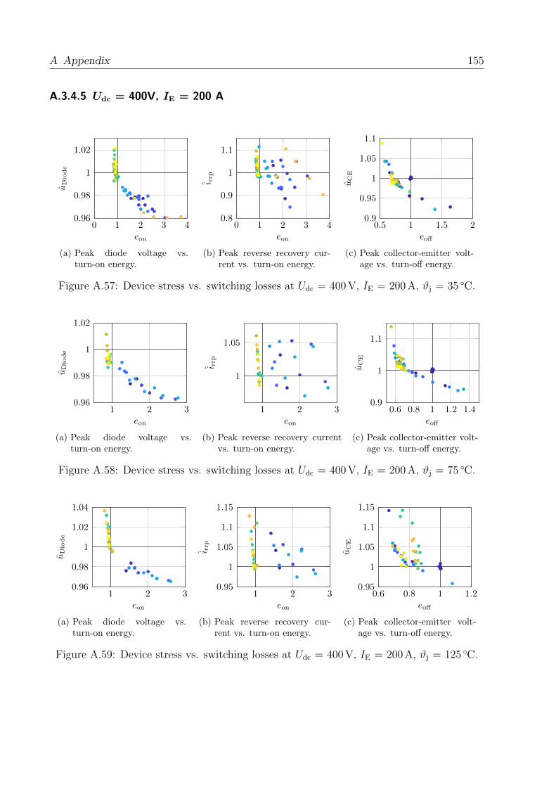
A Appendix 155
A.3.4.5 Udc = 400V, IE = 200 A
0 1 2 3 40.96
0.98
1
1.02
eon
uDiode
(a) Peak diode voltage vs.turn-on energy.
0 1 2 3 40.8
0.9
1
1.1
eon
i rrp
(b) Peak reverse recovery cur-rent vs. turn-on energy.
0.5 1 1.5 20.9
0.95
1
1.05
1.1
eoff
uC
E
(c) Peak collector-emitter volt-age vs. turn-off energy.
Figure A.57: Device stress vs. switching losses at Udc = 400 V, IE = 200 A, ϑj = 35 C.
1 2 30.96
0.98
1
1.02
eon
uDiode
(a) Peak diode voltage vs.turn-on energy.
1 2 3
1
1.05
eon
i rrp
(b) Peak reverse recovery currentvs. turn-on energy.
0.6 0.8 1 1.2 1.40.9
1
1.1
eoff
uC
E
(c) Peak collector-emitter volt-age vs. turn-off energy.
Figure A.58: Device stress vs. switching losses at Udc = 400 V, IE = 200 A, ϑj = 75 C.
1 2 30.96
0.98
1
1.02
1.04
eon
uDiode
(a) Peak diode voltage vs.turn-on energy.
1 2 30.95
1
1.05
1.1
1.15
eon
i rrp
(b) Peak reverse recovery cur-rent vs. turn-on energy.
0.6 0.8 1 1.20.95
1
1.05
1.1
1.15
eoff
uC
E
(c) Peak collector-emitter volt-age vs. turn-off energy.
Figure A.59: Device stress vs. switching losses at Udc = 400 V, IE = 200 A, ϑj = 125 C.

156 A.3 Active Gate Driver
A.3.4.6 Udc = 400V, IE = 300 A
0 1 2 3 40.96
0.97
0.98
0.99
1
eon
uDiode
(a) Peak diode voltage vs.turn-on energy.
0 1 2 3 4
0.9
1
1.1
eoni rrp
(b) Peak reverse recovery cur-rent vs. turn-on energy.
0.5 1 1.5 20.9
0.95
1
1.05
1.1
eoff
uC
E
(c) Peak collector-emitter volt-age vs. turn-off energy.
Figure A.60: Device stress vs. switching losses at Udc = 400 V, IE = 300 A, ϑj = 35 C.
0 1 2 3 40.96
0.98
1
eon
uDiode
(a) Peak diode voltage vs.turn-on energy.
0 1 2 3 40.95
1
1.05
1.1
1.15
eon
i rrp
(b) Peak reverse recovery cur-rent vs. turn-on energy.
0.5 1 1.5 20.9
0.95
1
1.05
1.1
eoff
uC
E
(c) Peak collector-emitter volt-age vs. turn-off energy.
Figure A.61: Device stress vs. switching losses at Udc = 400 V, IE = 300 A, ϑj = 75 C.
1 2 30.96
0.98
1
eon
uDiode
(a) Peak diode voltage vs.turn-on energy.
1 2 3
1
1.05
1.1
eon
i rrp
(b) Peak reverse recovery cur-rent vs. turn-on energy.
0.6 0.8 1 1.2 1.40.9
0.95
1
1.05
1.1
eoff
uC
E
(c) Peak collector-emitter volt-age vs. turn-off energy.
Figure A.62: Device stress vs. switching losses at Udc = 400 V, IE = 300 A, ϑj = 125 C.

B Acronyms
2D two dimensional3D three dimensional
AC alternative currentAGD active gate driverASIC application-specific integrated circuit
BMBF Bundesministerium fur Bildung und ForschungBNC Bayonet Neill-Concelman
CAD computer aided designCPLD complex programmable logic deviceCVR current viewing resistor
DAB dual active bridgeDBC direct bonded copperDC direct currentDCM digital clock managerDLL delay-locked loopDUT device under test
EMI elctromagnetic interferenceEV electric vehicle
FE finite elementFEM finite element methodFET field-effect transistorFPGA field-programmable gate array
GaN gallium nitrideGDU gate drive unit
I2C inter-integrated circuitIC integrated circuitIGBT insulated-gate bipolar transistorISEA Institut fur Stromrichtertechnik und Elektrische
Antriebe
157

158 Acronyms
LVDS low-voltage differential signaling
MCU microcontrollerMOSFET metal-oxide semiconductor field-effect transistor
NPT non-punch-through
PC personal computerPCB printed circuit boardPEM Power Electronic Measurements Ltd.PMK PMK Mess- & Kommunikationstechnik GmbHPV photovoltaic
Si siliconSiC silicon carbideSPICE simulation program with integrated circuit emphasis
TEC thermoelectric coolerTIM thermal interface materialTTL transistor-transistor logic
WBG wide-bandgap
C Symbols
~B 3D position-dependent B-field vector
CCE collector-emitter capacitanceCDC dc-link capacitorCDC− capacitance between the DC− terminal and the heat
sinkCDC+ capacitance between the DC+ terminal and the heat
sinkCDS drain-source capacitanceCG gate capacitanceCGC gate-collector capacitanceCGD gate-drain capacitanceCGE gate-emitter capacitanceCG,H capacitance between the high-side gate and the heat
sinkCG,L capacitance between the low-side gate and the heat sinkCGS gate-source capacitanceCH,A high-side capacitance, half-bridge A, B or CCies IGBT input capacitanceCiss MOSFET input capacitanceCL,A low-side capacitance, half-bridge A, B or CCoes IGBT output capacitanceCoss MOSFET output capacitanceCres IGBT reverse transfer capacitanceCrss MOSFET reverse transfer capacitanceCSW capacitance between the SW terminal and the heat sink
DC− negative DC terminalϕ phase shift of the DCMDC+ positive DC terminal
∆IE difference between peak emitter current and RMS emit-ter current
∆Irrp difference between reverse recovery current and RMSemitter current
∆IS difference between peak source current and load current∆tSnoff duration of the turn-off stage Sn
∆tSnon duration of the turn-on stage Sn
159

160 Symbols
∆UCE peak collector-emitter voltage
∆UDiode peak diode voltage excluding dc-link voltage
∆UDS difference between peak drain-source and dc-link volt-age
∆URefDS difference between reference peak drain-source and dc-
link voltage∆uMeas differential measured voltage
Eoff turn-off switching energyEoff,Diode diode turn-off switching energyeoff per unit turn-off switching energyERef
off turn-off switching energy using the reference driverEoff,Switch switch turn-off switching energyEon turn-on loss energy including diode turn-off losseseon per unit turn-on switching energy including diodeERef
on turn-on loss energy using the reference driver includingdiode turn-off losses
Eon,Switch switch turn-on switching energyεr relative permittivityEsw switching energy
f offosc oscillation frequency during turn-off eventf on
osc oscillation frequency during turn-on eventfres resonant frequencyfsw switching frequency
GH high-side gate terminalGH,A high-side gate terminal in half-bridge A, B or CGL low-side gate terminalGL,A low-side gate terminal in half-bridge A, B or CGND ground terminal
~H 3D position-dependent H-field vector
IBias RMS bias currentiC capacitor currentICn integrated circuit part niD instantaneous drain currentIdc dc load currentiDiode instantaneous diode current (high-side switch)iDUT current through device under testIE RMS emitter currentiE instantaneous emitter current
IE absolute peak emitter current

Symbols 161
iG instantaneous gate currentiH instantaneous current valueiL instantaneous inductor currentILoad RMS load currentiLoad instantaneous load currentIMeas RMS value of the impedance measurement currentp instantaneous poweriRCn current measured using a Rogowski coil
Irrp absolute reverse recovery peak current
irrp per unit reverse recovery peak current
IRefrrp reference absolute reverse recovery peak currentIS RMS value of the source currentiS instantaneous source current
IS peak source current
KE Kelvin emitter
LCE stray inductance in the collector pathLC,H high-side partial collector inductanceLC,L low-side partial collector inductanceLCS variable common-source inductanceLCS,HS high-side common-source inductanceLCS,LS low-side common-source inductanceLD drain inductanceLDC− dc-link inductance in the negative supplyLDC+ dc-link inductance in the positive supplyLD,H high-side diode inductanceLD,L low-side diode inductanceLDS drain-source inductanceLDUT inductance of the DUT used in the current pulse gen-
eratorLE,H high-side common emitter inductanceLE1,H stray inductance in the high-side emitter pathLE,L low-side common emitter inductanceLEn,L stray inductance in the low-side emitter pathLG gate inductanceLG variable gate inductance (high- and/or low-side)LG,HS high-side gate inductance, in half-bridge A, B or CL
′Gn,H high-side gate inductance n
LG,LS low-side gate inductance, in half-bridge A, B or CL
′Gn,L low-side gate inductance n
LGn gate inductance of IGBT nLGS gate-source inductanceLLoop total variable loop inductance

162 Symbols
LS source inductanceLσ,CVR stray inductance of the CVRLσ,DC dc-link stray inductanceLσ,Diode stray inductance in series to the diodeLσgate,ext external gate inductanceLσgate,int internal gate inductanceLσ,Switch stray inductance in series to the switchLσ stray inductanceLsw stray inductance in the SW output path
µr relative permeability
PCond conduction lossespDiode instantaneous losses in a diodePLoss sum of the switching and the conduction losses in a
semiconductor
P peak powerPSW switching lossespSW instantaneous losses in a switch
Qoff,n gate turn-off n-MOSFET in branch nQon,n gate turn-on p-MOSFET in branch n
RCVR current monitor resistanceRG gate resistanceRG,HS high-side gate resistorRG,int internal gate resistanceRG,LS low-side gate resistorRmax
G maximum IGBT gate resistanceRG,off gate turn-off resistanceRmin
G,off minimum IGBT turn-off gate resistanceRG,off,n turn-off gate resistance in branch nRRef
G,off reference turn-off gate resistanceRSn
G,off turn-off gate resistance during the stage Sn
RG,on gate turn-on resistanceRG,on,equiv equivalent gate resistanceRmin
G,on minimum IGBT turn-on gate resistanceRG,on,n turn-on gate resistance in branch nRSn
G,on turn-on gate resistance during the stage Sn
RH,A high-side resistance of the half-bridge A, B or CRσ stray resistance (current pulse fitting)
SDUT switch of the device under testσr specific electrical conductivity in S/m

Symbols 163
Sn IGBT no. nSv virtual source contactSW switched output terminal
t1 end timeϑj junction temperaturetOff turn-off timetSnoff start time of the turn-off stage Sn
tOn turn-on timetSnon start time of the turn-on stage Sn
t0 start time
U(BR)CEO collector-emitter breakdown voltageuC capacitor voltageUcc supply voltageuCE collector-emitter voltageuCE,H high-side collector-emitter voltageuCE,L low-side collector-emitter voltage
UCE peak collector-emitter voltageuCE per unit peak collector-emitter voltage
URefCE reference peak collector-emitter voltage
Udc dc-link voltageuDiode high-side emitter-collector voltage
UDiode peak diode voltage including dc-link voltageuDiode per unit peak diode voltage
URefDiode referene peak diode voltage
uDS drain-source voltage
UDS peak drain-source voltage (MOSFET)
URefDS reference drain-source peak voltage (MOSFET)
UDSS drain-to-source breakdown voltageuDUT voltage accross device under testuGD gate-drain voltageuGE gate-emitter voltageuGS low-side gate-source voltageUGS,off off-state gate-source voltageUGS,on on-state gate-source voltageUhv double pulse test high voltage supplyuL voltage accross an inductor LUlv double pulse test low voltage supplyuMeas instantaneous measured voltageUss negative supply voltageUth threshold voltage
WL electromagnetic energy stored in an inductor

164 Symbols
Wmag electromagnetic energyWmag
DS electromagnetic energy stored in the drain-source loopWmag
GDS electromagnetic energy stored in the gate-drain-sourceloop
WmagGS electromagnetic energy stored in the gate-source loop

Symbols 165

166

List of Figures
2.1 IGBT and MOSFET symbols. . . . . . . . . . . . . . . . . . . . . . . . . . . 7(a) IGBT symbol. . . . . . . . . . . . . . . . . . . . . . . . . . . . . . . . . 7(b) MOSFET symbol. . . . . . . . . . . . . . . . . . . . . . . . . . . . . . 7
2.2 IGBT and MOSFET symbols including capacitances that have the greatesteffect on the switching. . . . . . . . . . . . . . . . . . . . . . . . . . . . . . . 8(a) IGBT symbol. . . . . . . . . . . . . . . . . . . . . . . . . . . . . . . . . 8(b) MOSFET symbol. . . . . . . . . . . . . . . . . . . . . . . . . . . . . . 8
2.3 Half bridge configurations. . . . . . . . . . . . . . . . . . . . . . . . . . . . . 9(a) IGBT halfbridge. . . . . . . . . . . . . . . . . . . . . . . . . . . . . . . 9(b) MOSFET halfbridge. . . . . . . . . . . . . . . . . . . . . . . . . . . . . 9
2.4 Exemplary switching waveform of an IGBT. . . . . . . . . . . . . . . . . . . 9(a) Turn-on event. . . . . . . . . . . . . . . . . . . . . . . . . . . . . . . . 9(b) Turn-off event. . . . . . . . . . . . . . . . . . . . . . . . . . . . . . . . 9
2.5 Exemplary waveforms of a double pulse measurement. . . . . . . . . . . . . . 11(a) Exemplary double pulse waveform. . . . . . . . . . . . . . . . . . . . . 11(b) Zoomed-in waveforms. . . . . . . . . . . . . . . . . . . . . . . . . . . . 11
2.6 Switching events. . . . . . . . . . . . . . . . . . . . . . . . . . . . . . . . . . 12(a) Qualitative waveforms of a turn-off event. . . . . . . . . . . . . . . . . 12(b) Qualitative waveforms of a turn-on event. . . . . . . . . . . . . . . . . 12
2.7 Typical low- and high-side gate driving circuit. . . . . . . . . . . . . . . . . . 132.8 Different power semiconductor packages. . . . . . . . . . . . . . . . . . . . . 16
(a) DirectFET™. . . . . . . . . . . . . . . . . . . . . . . . . . . . . . . . . 16(b) TO-247. . . . . . . . . . . . . . . . . . . . . . . . . . . . . . . . . . . . 16(c) SOT-227-4. . . . . . . . . . . . . . . . . . . . . . . . . . . . . . . . . . 16
2.9 Side cut through a power package. . . . . . . . . . . . . . . . . . . . . . . . . 162.10 Current pulse generator. . . . . . . . . . . . . . . . . . . . . . . . . . . . . . 19
(a) Topology. . . . . . . . . . . . . . . . . . . . . . . . . . . . . . . . . . . 19(b) Photograph. . . . . . . . . . . . . . . . . . . . . . . . . . . . . . . . . . 19
2.11 Agilent 4294A Impedance Analyzer. . . . . . . . . . . . . . . . . . . . . . . . 202.12 Impedance analyzer fit circuits. . . . . . . . . . . . . . . . . . . . . . . . . . 20
(a) Parallel RLC. . . . . . . . . . . . . . . . . . . . . . . . . . . . . . . . . 20(b) Series RLC. . . . . . . . . . . . . . . . . . . . . . . . . . . . . . . . . . 20
2.13 Topology of the double pulse test bench. . . . . . . . . . . . . . . . . . . . . 202.14 Photograph of the temperature unit. . . . . . . . . . . . . . . . . . . . . . . 21
3.1 Parasitic inductances in a half bridge. . . . . . . . . . . . . . . . . . . . . . . 243.2 Partial inductance including resistive part. . . . . . . . . . . . . . . . . . . . 26
167

168 List of Figures
3.3 Exemplary waveforms of a partial inductance measurement. . . . . . . . . . 263.4 Photograph of the HybridPACK™2. . . . . . . . . . . . . . . . . . . . . . . . 273.5 Photograph of the extracted DBC substrate. . . . . . . . . . . . . . . . . . . 283.6 CAD model of the extracted DBC substrate. . . . . . . . . . . . . . . . . . . 283.7 Photograph of the extracted DBC substrate with terminal lugs for the impedance
measurement. . . . . . . . . . . . . . . . . . . . . . . . . . . . . . . . . . . . 303.8 Simulation model for the determination of the power loop inductance. . . . . 313.9 Current distribution at different frequencies f . . . . . . . . . . . . . . . . . . 32
(a) f = 1 kHz. . . . . . . . . . . . . . . . . . . . . . . . . . . . . . . . . . . 32(b) f = 100 kHz. . . . . . . . . . . . . . . . . . . . . . . . . . . . . . . . . 32
3.10 Low- and high-side gate loop path simulation models. . . . . . . . . . . . . . 32(a) High-side gate loop path. . . . . . . . . . . . . . . . . . . . . . . . . . 32(b) Low-side gate loop path. . . . . . . . . . . . . . . . . . . . . . . . . . . 32
3.11 Test setup for the power loop inductance determination. . . . . . . . . . . . 34(a) Schematic of the test setup. . . . . . . . . . . . . . . . . . . . . . . . . 34(b) HybridPACK™2 with fixture PCB. . . . . . . . . . . . . . . . . . . . . 34
3.12 Test setup to determine the gate loop inductances. . . . . . . . . . . . . . . 34(a) Schematic of the low-side test setup. . . . . . . . . . . . . . . . . . . . 34(b) Photograph of the PCB fixture. . . . . . . . . . . . . . . . . . . . . . . 34
3.13 Circuit showing the double pulse test power loop. . . . . . . . . . . . . . . . 35(a) Circuit of the low-side measurement setup. . . . . . . . . . . . . . . . . 35(b) Circuit of the high-side measurement setup. . . . . . . . . . . . . . . . 35
3.14 Double pulse measurement for the determination of LD,L. . . . . . . . . . . . 363.15 Measurement setup for the partial inductances. . . . . . . . . . . . . . . . . 37
(a) Rogowski coil placement and measurement points. . . . . . . . . . . . . 37(b) Measured waveforms to determine LDC+. . . . . . . . . . . . . . . . . . 37
3.16 Determined partial inductances. . . . . . . . . . . . . . . . . . . . . . . . . . 383.17 SiC MOSFET in a TO-247 pacakage. . . . . . . . . . . . . . . . . . . . . . . 39
(a) Photograph of an opened TO-247 package. . . . . . . . . . . . . . . . . 39(b) 3D CAD model of the package. . . . . . . . . . . . . . . . . . . . . . . 39
3.18 TO-247 package simulation setup. . . . . . . . . . . . . . . . . . . . . . . . . 40(a) Gate-source excitation. . . . . . . . . . . . . . . . . . . . . . . . . . . . 40(b) Drain-source excitation. . . . . . . . . . . . . . . . . . . . . . . . . . . 40(c) Gate- and drain-source excitation. . . . . . . . . . . . . . . . . . . . . . 40(d) Schematic. . . . . . . . . . . . . . . . . . . . . . . . . . . . . . . . . . . 40
3.19 Simulation results. . . . . . . . . . . . . . . . . . . . . . . . . . . . . . . . . 41(a) Simulation results of the TO-247 package inductances using a lead
length l = 7 mm. . . . . . . . . . . . . . . . . . . . . . . . . . . . . . . 41(b) Current density of the TO-247 package at f = 1 MHz for the drain
excitation. . . . . . . . . . . . . . . . . . . . . . . . . . . . . . . . . . . 413.20 Partial inductance extraction test setup of the TO-247 package. . . . . . . . 42
(a) Schematic of the setup. . . . . . . . . . . . . . . . . . . . . . . . . . . . 42(b) Photograph of the setup including the measurement probes. . . . . . . 42
3.21 Waveforms of the current pulse measurements. . . . . . . . . . . . . . . . . . 43(a) Measurement and fitting results for LD. . . . . . . . . . . . . . . . . . 43
List of Figures 169
(b) Measurement and fitting results for LS. . . . . . . . . . . . . . . . . . . 43
(c) Measurement and fitting results for LDS. . . . . . . . . . . . . . . . . . 43
3.22 Simplified model. . . . . . . . . . . . . . . . . . . . . . . . . . . . . . . . . . 44
3.23 Detailed model. . . . . . . . . . . . . . . . . . . . . . . . . . . . . . . . . . . 45
3.24 Comparison between the turn-on experimental and simulated switching eventsfor Udc = 400 V and ϑj = 30 C. . . . . . . . . . . . . . . . . . . . . . . . . . 47
(a) Turn-on event at IE = 25 A. . . . . . . . . . . . . . . . . . . . . . . . . 47
(b) Turn-on event at IE = 90 A. . . . . . . . . . . . . . . . . . . . . . . . . 47
(c) Turn-on event at IE = 200 A. . . . . . . . . . . . . . . . . . . . . . . . 47
3.25 Comparison between the turn-off experimental and simulated switching eventsfor Udc = 400 V and ϑj = 30 C. . . . . . . . . . . . . . . . . . . . . . . . . . 48
(a) Turn-off event at IE = 25 A. . . . . . . . . . . . . . . . . . . . . . . . . 48
(b) Turn-off event at IE = 90 A. . . . . . . . . . . . . . . . . . . . . . . . . 48
(c) Turn-off event at IE = 200 A. . . . . . . . . . . . . . . . . . . . . . . . 48
4.1 Schematic of the switching cell with variable inductances. . . . . . . . . . . . 52
4.2 Photograph of the PCB with variable inductances. . . . . . . . . . . . . . . . 52
4.3 Variable inductance setup. . . . . . . . . . . . . . . . . . . . . . . . . . . . . 53
(a) Pin header as variable inductance adjustment. . . . . . . . . . . . . . . 53
(b) Measured power loop inductance LLoop depending on jumper position. . 53
4.4 Close-up view on the common-source inductance variation setup. . . . . . . . 54
4.5 Switching transients for various low-side loop-inductances LLoop at Udc = 200 V,IS = 100 A, RG,LS = 5.6 Ω, LG,LS = LG,HS = 4.9 nH and LCS,LS = 0 nH. . . . 55
(a) Turn-on event. . . . . . . . . . . . . . . . . . . . . . . . . . . . . . . . 55
(b) Turn-off event. . . . . . . . . . . . . . . . . . . . . . . . . . . . . . . . 55
4.6 Equivalent circuit during the switching events. . . . . . . . . . . . . . . . . . 56
(a) Turn-on equivalent circuit. . . . . . . . . . . . . . . . . . . . . . . . . . 56
(b) Turn-off equivalent circuit. . . . . . . . . . . . . . . . . . . . . . . . . . 56
4.7 Turn-on event waveforms for various low-side common-source inductancesusing Udc = 200 V. . . . . . . . . . . . . . . . . . . . . . . . . . . . . . . . . 58
(a) Waveforms for RG,LS = 5.6 Ω, IS = 100 A . . . . . . . . . . . . . . . . . 58
(b) Waveforms for RG,LS = 0 Ω, IS = 80 A . . . . . . . . . . . . . . . . . . 58
4.8 Turn-off event waveforms for various low-side common-source inductancesusing Udc = 200 V. . . . . . . . . . . . . . . . . . . . . . . . . . . . . . . . . 59
(a) Waveforms at RG,LS = 5.6 Ω, IS = 100 A. . . . . . . . . . . . . . . . . . 59
(b) Waveforms at RG,LS = 0 Ω, IS = 80 A. . . . . . . . . . . . . . . . . . . 59
4.9 Switching transient waveforms for various low-side gate inductances at Udc = 200 V,IS = 100 A and RG,LS = 5.6 Ω. . . . . . . . . . . . . . . . . . . . . . . . . . . 60
(a) Turn-on event. . . . . . . . . . . . . . . . . . . . . . . . . . . . . . . . 60
(b) Turn-off event. . . . . . . . . . . . . . . . . . . . . . . . . . . . . . . . 60
4.10 Device stress vs. power loop inductance LLoop at Udc = 200 V and RG,LS = 5.6 Ω. 62
(a) Low-side voltage stress. . . . . . . . . . . . . . . . . . . . . . . . . . . 62
(b) High-side voltage stress. . . . . . . . . . . . . . . . . . . . . . . . . . . 62
(c) Current stress. . . . . . . . . . . . . . . . . . . . . . . . . . . . . . . . 62

170 List of Figures
4.11 Turn-on current slopes vs. power loop inductance LLoop using RG,LS = 0 Ω. . 62(a) Udc = 200 V. . . . . . . . . . . . . . . . . . . . . . . . . . . . . . . . . 62(b) Udc = 400 V. . . . . . . . . . . . . . . . . . . . . . . . . . . . . . . . . 62
4.12 Device stress vs. individual turn-on and turn-off losses Eon and Eoff andtotal losses Esw for different power loop inductances LLoop at Udc = 200 V,IS = 100 A and RG,LS = 5.6 Ω. . . . . . . . . . . . . . . . . . . . . . . . . . . 63(a) Low-side voltage stress. . . . . . . . . . . . . . . . . . . . . . . . . . . 63(b) High-side voltage stress. . . . . . . . . . . . . . . . . . . . . . . . . . . 63(c) Current stress. . . . . . . . . . . . . . . . . . . . . . . . . . . . . . . . 63(d) Low-side voltage stress. . . . . . . . . . . . . . . . . . . . . . . . . . . 63(e) High-side voltage stress. . . . . . . . . . . . . . . . . . . . . . . . . . . 63(f) Current stress. . . . . . . . . . . . . . . . . . . . . . . . . . . . . . . . 63
4.13 Device stress vs. low-side common-source inductance LCS,LS at Udc = 200 Vand RG,LS = 5.6 Ω. . . . . . . . . . . . . . . . . . . . . . . . . . . . . . . . . 64(a) Low-side voltage stress. . . . . . . . . . . . . . . . . . . . . . . . . . . 64(b) High-side voltage stress. . . . . . . . . . . . . . . . . . . . . . . . . . . 64(c) Current stress. . . . . . . . . . . . . . . . . . . . . . . . . . . . . . . . 64
4.14 Device stress vs. low-side common-source inductance LCS,LS at Udc = 200 Vand RG,LS = 0 Ω. . . . . . . . . . . . . . . . . . . . . . . . . . . . . . . . . . 64(a) Low-side voltage stress. . . . . . . . . . . . . . . . . . . . . . . . . . . 64(b) High-side voltage stress. . . . . . . . . . . . . . . . . . . . . . . . . . . 64(c) Current stress. . . . . . . . . . . . . . . . . . . . . . . . . . . . . . . . 64
4.15 Device stress vs. switching losses Esw for different common-source induc-tances at Udc = 200 V, IS = 100 A and RG,LS = 5.6 Ω. . . . . . . . . . . . . . 65(a) Low-side voltage stress. . . . . . . . . . . . . . . . . . . . . . . . . . . 65(b) High-side voltage stress. . . . . . . . . . . . . . . . . . . . . . . . . . . 65(c) Current stress. . . . . . . . . . . . . . . . . . . . . . . . . . . . . . . . 65
4.16 Device stress vs. switching losses Esw for different common-source induc-tances at Udc = 200 V, IS = 80 A, RG,LS = 0 Ω. . . . . . . . . . . . . . . . . . 66(a) Low-side voltage stress. . . . . . . . . . . . . . . . . . . . . . . . . . . 66(b) High-side voltage stress. . . . . . . . . . . . . . . . . . . . . . . . . . . 66(c) Current stress. . . . . . . . . . . . . . . . . . . . . . . . . . . . . . . . 66
4.17 Device stress vs. low-side gate ind. LG,LS at Udc = 200 V and RG,LS = 5.6 Ω. 67(a) Low-side voltage stress. . . . . . . . . . . . . . . . . . . . . . . . . . . 67(b) High-side voltage stress. . . . . . . . . . . . . . . . . . . . . . . . . . . 67(c) Current stress. . . . . . . . . . . . . . . . . . . . . . . . . . . . . . . . 67
4.18 Device stress vs. switching losses Esw for different low-side gate inductancesLG,LS at Udc = 200 V, IS = 100 A and RG,LS = 5.6 Ω. . . . . . . . . . . . . . 67(a) Low-side voltage stress. . . . . . . . . . . . . . . . . . . . . . . . . . . 67(b) High-side voltage stress. . . . . . . . . . . . . . . . . . . . . . . . . . . 67(c) Current stress. . . . . . . . . . . . . . . . . . . . . . . . . . . . . . . . 67
5.1 Block diagram of the driver structure. . . . . . . . . . . . . . . . . . . . . . . 725.2 Stage-wise gate driver topology. . . . . . . . . . . . . . . . . . . . . . . . . . 735.3 Operation principle of the stage-wise gate driver for the turn-on event. . . . 74

List of Figures 171
5.4 Stage-wise driver PCB. . . . . . . . . . . . . . . . . . . . . . . . . . . . . . . 765.5 Testing of the gate driver using a dummy capacitor. . . . . . . . . . . . . . . 77
(a) Capacitor voltage uC. . . . . . . . . . . . . . . . . . . . . . . . . . . . . 77(b) Capacitor current iC. . . . . . . . . . . . . . . . . . . . . . . . . . . . . 77
5.6 Gate charging artifact simulation. . . . . . . . . . . . . . . . . . . . . . . . . 77(a) Simulation circuit. . . . . . . . . . . . . . . . . . . . . . . . . . . . . . 77(b) Simulation results compared to measurement. . . . . . . . . . . . . . . 77
5.7 Schematic of the measurement setup and power module. . . . . . . . . . . . 785.8 IGBT reference driver and behavioral model. . . . . . . . . . . . . . . . . . . 79
(a) Photograph of the gate driver board. . . . . . . . . . . . . . . . . . . . 79(b) Behavioral model. . . . . . . . . . . . . . . . . . . . . . . . . . . . . . 79
5.9 Reference driver switching transients at Udc = 400 V. . . . . . . . . . . . . . 79(a) Turn-on event at IE = 100 A . . . . . . . . . . . . . . . . . . . . . . . . 79(b) Turn-off event at IE = 300 A . . . . . . . . . . . . . . . . . . . . . . . . 79
5.10 Reference driver switching losses using. . . . . . . . . . . . . . . . . . . . . . 80(a) Switch turn-on losses. . . . . . . . . . . . . . . . . . . . . . . . . . . . 80(b) Diode turn-off losses during the switch turn-on event. . . . . . . . . . . 80(c) Switch turn-off losses. . . . . . . . . . . . . . . . . . . . . . . . . . . . 80
5.11 Device stress using the reference driver. . . . . . . . . . . . . . . . . . . . . . 81(a) Reverse recovery peak current ∆Irrp. . . . . . . . . . . . . . . . . . . . 81
(b) Switch voltage overshoot ∆UCE. . . . . . . . . . . . . . . . . . . . . . . 81(c) Diode voltage overshoot ∆UDiode. . . . . . . . . . . . . . . . . . . . . . 81
5.12 Turn-off event using different gate resistors at Udc = 400 V, IE = 300 A,ϑj = 35 C. . . . . . . . . . . . . . . . . . . . . . . . . . . . . . . . . . . . . . 82
5.13 Influence of the two-stage turn-off event at Udc = 200 V, IE = 100 A, ϑj = 35 C. 83(a) Switching transients. . . . . . . . . . . . . . . . . . . . . . . . . . . . . 83(b) Loss power and energy. . . . . . . . . . . . . . . . . . . . . . . . . . . . 83
5.14 Various three-stage turn-off events at Udc = 200 V, IE = 200 A and ϑj = 125 C. 84(a) Switch waveforms. . . . . . . . . . . . . . . . . . . . . . . . . . . . . . 84(b) Switching losses. . . . . . . . . . . . . . . . . . . . . . . . . . . . . . . 84
5.15 Influence of the 2nd stage turn-on event at Udc = 200 V, IE = 200 A, ϑj = 35 C. 85(a) Switch waveforms. . . . . . . . . . . . . . . . . . . . . . . . . . . . . . 85(b) Diode waveforms. . . . . . . . . . . . . . . . . . . . . . . . . . . . . . . 85
5.16 Instantaneous losses and energies of the of the two-stage turn-on event atUdc = 200 V, IE = 200 A, ϑj = 35 C. . . . . . . . . . . . . . . . . . . . . . . 86(a) Switch energy and losses. . . . . . . . . . . . . . . . . . . . . . . . . . 86(b) Diode energy and losses. . . . . . . . . . . . . . . . . . . . . . . . . . . 86
5.17 Influence of the 3rd stage on the turn-on event at Udc = 200 V, IE = 100 A,ϑj = 35 C. . . . . . . . . . . . . . . . . . . . . . . . . . . . . . . . . . . . . . 86(a) Switch waveforms. . . . . . . . . . . . . . . . . . . . . . . . . . . . . . 86(b) Diode waveforms. . . . . . . . . . . . . . . . . . . . . . . . . . . . . . . 86
5.18 Turn-on energy using the 3rd stage at Udc = 200 V, IE = 100 A and ϑj = 35 C. 87(a) Switch losses. . . . . . . . . . . . . . . . . . . . . . . . . . . . . . . . . 87(b) Diode losses. . . . . . . . . . . . . . . . . . . . . . . . . . . . . . . . . 87

172 List of Figures
5.19 Turn-off optimization flow charts. . . . . . . . . . . . . . . . . . . . . . . . . 89(a) Two-stage turn-off optimization flow chart. . . . . . . . . . . . . . . . . 89(b) Three-stage turn-off optimization flow chart. . . . . . . . . . . . . . . . 89
5.20 Turn-on optimization flow charts. . . . . . . . . . . . . . . . . . . . . . . . . 91(a) Two-stage turn-on optimization flow chart. . . . . . . . . . . . . . . . . 91(b) Three-stage turn-on optimization flow chart. . . . . . . . . . . . . . . . 91
5.21 Device stress vs. switching energy at Udc = 400 V, IE = 200 A, ϑj = 35 Cusing various gate driver configurations (colored dots). . . . . . . . . . . . . 93(a) Peak collector-emitter voltage vs. turn-off energy. . . . . . . . . . . . . 93(b) Peak diode voltage vs. turn-on energy. . . . . . . . . . . . . . . . . . . 93(c) Reverse recovery peak current vs. turn-on energy. . . . . . . . . . . . . 93
5.22 Comparison of reference and optimized losses for equal device stress. . . . . . 94(a) Turn-on losses at ϑj = 75 C. . . . . . . . . . . . . . . . . . . . . . . . 94(b) Turn-off losses at ϑj = 35 C. . . . . . . . . . . . . . . . . . . . . . . . 94
5.23 Exemplary switching improvement using the stage-wise driver at Udc = 200 V,IE = 300 A, ϑj = 35 C. . . . . . . . . . . . . . . . . . . . . . . . . . . . . . . 95(a) Turn-off waveforms. . . . . . . . . . . . . . . . . . . . . . . . . . . . . 95(c) Turn-off losses. . . . . . . . . . . . . . . . . . . . . . . . . . . . . . . . 95(b) Turn-on waveforms. . . . . . . . . . . . . . . . . . . . . . . . . . . . . . 95(d) Turn-on losses. . . . . . . . . . . . . . . . . . . . . . . . . . . . . . . . 95
5.24 Schematic of the switching cell. . . . . . . . . . . . . . . . . . . . . . . . . . 975.25 Schematic of a single branch of the stage-wise gate driver. . . . . . . . . . . 975.26 PCB containing the gate driver and SiC bare die MOSFETs. . . . . . . . . . 98
(a) Gate driver board. . . . . . . . . . . . . . . . . . . . . . . . . . . . . . 98(b) Close up view on the low-side MOSFET. . . . . . . . . . . . . . . . . . 98
5.27 Front and back side view of the control board. . . . . . . . . . . . . . . . . . 98(a) Bottom View. . . . . . . . . . . . . . . . . . . . . . . . . . . . . . . . . 98(b) Top View. . . . . . . . . . . . . . . . . . . . . . . . . . . . . . . . . . . 98
5.28 Delay-locked loop waveform. . . . . . . . . . . . . . . . . . . . . . . . . . . . 995.29 Measurement setup of the switching cell. . . . . . . . . . . . . . . . . . . . . 99
(a) Measurement setup. . . . . . . . . . . . . . . . . . . . . . . . . . . . . 99(b) Close-up view. . . . . . . . . . . . . . . . . . . . . . . . . . . . . . . . 99
5.30 Modifications of the AGD to form the reference gate driver. . . . . . . . . . 1005.31 Measured waveforms using the reference driver. . . . . . . . . . . . . . . . . 101
(a) Turn-on event. . . . . . . . . . . . . . . . . . . . . . . . . . . . . . . . 101(b) Turn-off event. . . . . . . . . . . . . . . . . . . . . . . . . . . . . . . . 101
5.32 Switching energy vs. gate resistance RG at Udc = 700 V and IS = 60 A. . . . 1025.33 Device stress vs. switching energy using the reference driver. . . . . . . . . . 102
(a) Switch current stress during the turn-on event. . . . . . . . . . . . . . 102(b) Diode voltage stress during the turn-on event. . . . . . . . . . . . . . . 102(c) Switch voltage stress during the turn-off event. . . . . . . . . . . . . . 102
5.34 Investigations on the two-stage turn-off event. . . . . . . . . . . . . . . . . . 103(a) Waveforms using RS2
G,off = 15 Ω. . . . . . . . . . . . . . . . . . . . . . . 103(b) Peak voltage vs. turn-off energy. . . . . . . . . . . . . . . . . . . . . . 103

List of Figures 173
5.35 Three-stage turn-off event variation. . . . . . . . . . . . . . . . . . . . . . . . 104(a) Three-stage turn-off waveforms. . . . . . . . . . . . . . . . . . . . . . . 104(b) Three-stage turn-off evaluation. . . . . . . . . . . . . . . . . . . . . . . 104
5.36 Two-stage turn-on variation using RS2G,on = 10 Ω. . . . . . . . . . . . . . . . . 105
(a) Switch waveforms. . . . . . . . . . . . . . . . . . . . . . . . . . . . . . 105(b) Diode waveforms. . . . . . . . . . . . . . . . . . . . . . . . . . . . . . . 105
5.37 Two-stage turn-on evaluation. . . . . . . . . . . . . . . . . . . . . . . . . . . 106(a) Diode overshoot Voltage. . . . . . . . . . . . . . . . . . . . . . . . . . . 106(b) Reverse recovery current. . . . . . . . . . . . . . . . . . . . . . . . . . 106
5.38 Three-stage turn-on operation. . . . . . . . . . . . . . . . . . . . . . . . . . . 107(a) Switch waveforms. . . . . . . . . . . . . . . . . . . . . . . . . . . . . . 107(b) Diode waveforms. . . . . . . . . . . . . . . . . . . . . . . . . . . . . . . 107
5.39 Three-stage turn-on event evaluation. . . . . . . . . . . . . . . . . . . . . . . 108(a) Diode overshoot voltage vs. turn-on energy. . . . . . . . . . . . . . . . 108(b) Peak source current vs. turn-on energy. . . . . . . . . . . . . . . . . . . 108
5.40 Absolute improvements using the three-stage SiC AGD. . . . . . . . . . . . . 110(b) Current peak vs. turn-on energy. . . . . . . . . . . . . . . . . . . . . . 110(c) Diode peak voltage vs. turn-on energy. . . . . . . . . . . . . . . . . . . 110(d) Switch peak voltage vs. turn-off energy. . . . . . . . . . . . . . . . . . 110
6.1 Extrapolation of device stress vs. power loop inductance LLoop at Udc = 200 Vand 400 V. . . . . . . . . . . . . . . . . . . . . . . . . . . . . . . . . . . . . . 116(a) RG,LS = 0 Ω. . . . . . . . . . . . . . . . . . . . . . . . . . . . . . . . . 116(b) RG,LS = 5.6 Ω. . . . . . . . . . . . . . . . . . . . . . . . . . . . . . . . 116
A.1 Switching transients for various low-side loop-inductances LLoop at Udc = 200 V,IS = 100 A, RG,LS = 0 Ω, LG,LS = LG,HS = 4.9 nH and LCS,LS = 0 nH. . . . . 125(a) Turn-on event. . . . . . . . . . . . . . . . . . . . . . . . . . . . . . . . 125(b) Turn-off event. . . . . . . . . . . . . . . . . . . . . . . . . . . . . . . . 125
A.2 Switching transients for various low-side loop-inductances LLoop at Udc = 400 V,IS = 100 A, RG,LS = 0 Ω, LG,LS = LG,HS = 4.9 nH and LCS,LS = 0 nH. . . . . 126(a) Turn-on event. . . . . . . . . . . . . . . . . . . . . . . . . . . . . . . . 126(b) Turn-off event. . . . . . . . . . . . . . . . . . . . . . . . . . . . . . . . 126
A.3 Switching transients for various low-side loop-inductances LLoop at Udc = 400 V,IS = 100 A, RG,LS = 5.6 Ω, LG,LS = LG,HS = 4.9 nH and LCS,LS = 0 nH. . . . 126(a) Turn-on event. . . . . . . . . . . . . . . . . . . . . . . . . . . . . . . . 126(b) Turn-off event. . . . . . . . . . . . . . . . . . . . . . . . . . . . . . . . 126
A.4 Variation of the low-side common-source inductance LCS,LS using Udc = 200 V,IS = 100 A, RG,LS = 0 Ω. . . . . . . . . . . . . . . . . . . . . . . . . . . . . . 127(a) Turn-off event. . . . . . . . . . . . . . . . . . . . . . . . . . . . . . . . 127(b) Turn-on event. . . . . . . . . . . . . . . . . . . . . . . . . . . . . . . . 127
A.5 Variation of the low-side common-source inductance LCS,LS using Udc = 400 V,IS = 100 A, RG,LS = 5.6 Ω. . . . . . . . . . . . . . . . . . . . . . . . . . . . . 128(a) Turn-off event. . . . . . . . . . . . . . . . . . . . . . . . . . . . . . . . 128(b) Turn-on event. . . . . . . . . . . . . . . . . . . . . . . . . . . . . . . . 128

174 List of Figures
A.6 Turn-on event waveforms for various high-side common-source inductancesat Udc = 200 V IS = 100 A and RG,LS = 0 Ω. . . . . . . . . . . . . . . . . . . 129(a) Turn-on event. . . . . . . . . . . . . . . . . . . . . . . . . . . . . . . . 129(b) Turn-off event. . . . . . . . . . . . . . . . . . . . . . . . . . . . . . . . 129
A.7 Turn-on event waveforms for various high-side common-source inductancesat Udc = 200 V IS = 100 A and RG,LS = 5.6 Ω. . . . . . . . . . . . . . . . . . 129(a) Turn-on event. . . . . . . . . . . . . . . . . . . . . . . . . . . . . . . . 129(b) Turn-off event. . . . . . . . . . . . . . . . . . . . . . . . . . . . . . . . 129
A.8 Turn-on event waveforms for various high-side common-source inductancesat Udc = 400 V IS = 100 A and RG,LS = 0 Ω. . . . . . . . . . . . . . . . . . . 130(a) Turn-on event. . . . . . . . . . . . . . . . . . . . . . . . . . . . . . . . 130(b) Turn-off event. . . . . . . . . . . . . . . . . . . . . . . . . . . . . . . . 130
A.9 Turn-on event waveforms for various high-side common-source inductancesat Udc = 400 V IS = 100 A and RG,LS = 5.6 Ω. . . . . . . . . . . . . . . . . . 130(a) Turn-on event. . . . . . . . . . . . . . . . . . . . . . . . . . . . . . . . 130(b) Turn-off event. . . . . . . . . . . . . . . . . . . . . . . . . . . . . . . . 130
A.10 Switching waveforms for various low-side gate inductances at Udc = 200 V,IS = 100 A and RG,LS = 0 Ω. . . . . . . . . . . . . . . . . . . . . . . . . . . . 131(a) Turn-on event. . . . . . . . . . . . . . . . . . . . . . . . . . . . . . . . 131(b) Turn-off event. . . . . . . . . . . . . . . . . . . . . . . . . . . . . . . . 131
A.11 Switching waveforms for various low-side gate inductances at Udc = 400 V,IS = 100 A and RG,LS = 0 Ω. . . . . . . . . . . . . . . . . . . . . . . . . . . . 131(a) Turn-on event. . . . . . . . . . . . . . . . . . . . . . . . . . . . . . . . 131(b) Turn-off event. . . . . . . . . . . . . . . . . . . . . . . . . . . . . . . . 131
A.12 Switching waveforms for various low-side gate inductances at Udc = 400 V,IS = 100 A and RG,LS = 5.6 Ω. . . . . . . . . . . . . . . . . . . . . . . . . . . 132(a) Turn-on event. . . . . . . . . . . . . . . . . . . . . . . . . . . . . . . . 132(b) Turn-off event. . . . . . . . . . . . . . . . . . . . . . . . . . . . . . . . 132
A.13 Turn-on event waveforms for various high-side gate inductances at Udc = 200 V,IS = 100 A and RG,LS = 0 Ω. . . . . . . . . . . . . . . . . . . . . . . . . . . . 133(a) Turn-on event. . . . . . . . . . . . . . . . . . . . . . . . . . . . . . . . 133(b) Turn-off event. . . . . . . . . . . . . . . . . . . . . . . . . . . . . . . . 133
A.14 Turn-on event waveforms for various high-side gate inductances at Udc = 200 V,IS = 100 A and RG,LS = 5.6 Ω. . . . . . . . . . . . . . . . . . . . . . . . . . . 133(a) Turn-on event. . . . . . . . . . . . . . . . . . . . . . . . . . . . . . . . 133(b) Turn-off event. . . . . . . . . . . . . . . . . . . . . . . . . . . . . . . . 133
A.15 Turn-on event waveforms for various high-side gate inductances at Udc = 400 V,IS = 100 A and RG,LS = 0 Ω. . . . . . . . . . . . . . . . . . . . . . . . . . . . 134(a) Turn-on event. . . . . . . . . . . . . . . . . . . . . . . . . . . . . . . . 134(b) Turn-off event. . . . . . . . . . . . . . . . . . . . . . . . . . . . . . . . 134
A.16 Turn-on event waveforms for various high-side gate inductances at Udc = 400 V,ILoad = 100 A and RG,LS = 5.6 Ω. . . . . . . . . . . . . . . . . . . . . . . . . 134(a) Turn-on event. . . . . . . . . . . . . . . . . . . . . . . . . . . . . . . . 134(b) Turn-off event. . . . . . . . . . . . . . . . . . . . . . . . . . . . . . . . 134

List of Figures 175
A.17 Device stress vs. power loop inductance at Udc = 200 V and RG,LS = 0 Ω. . . 135(a) Low-side voltage stress. . . . . . . . . . . . . . . . . . . . . . . . . . . 135(b) High-side voltage stress. . . . . . . . . . . . . . . . . . . . . . . . . . . 135(c) Low-side current stress. . . . . . . . . . . . . . . . . . . . . . . . . . . 135
A.18 Device stress vs. power loop inductance at Udc = 400 V and RG,LS = 0 Ω. . . 135(a) Low-side voltage stress. . . . . . . . . . . . . . . . . . . . . . . . . . . 135(b) High-side voltage stress. . . . . . . . . . . . . . . . . . . . . . . . . . . 135(c) Low-side current stress. . . . . . . . . . . . . . . . . . . . . . . . . . . 135
A.19 Device stress vs. power loop inductance at Udc = 400 V and RG,LS = 5.6 Ω. . 135(a) Low-side voltage stress. . . . . . . . . . . . . . . . . . . . . . . . . . . 135(b) High-side voltage stress. . . . . . . . . . . . . . . . . . . . . . . . . . . 135(c) Low-side current stress. . . . . . . . . . . . . . . . . . . . . . . . . . . 135
A.20 Turn-on current slopes vs. power loop inductance LLoop using RG,LS = 5.6 Ω. 136(a) Udc = 200 V. . . . . . . . . . . . . . . . . . . . . . . . . . . . . . . . . 136(b) Udc = 400 V. . . . . . . . . . . . . . . . . . . . . . . . . . . . . . . . . 136
A.21 Device stress vs. switching losses for different power loop inductances LLoop
at Udc = 200 V, IS = 100 A and RG,LS = 0 Ω. . . . . . . . . . . . . . . . . . . 136(a) Low-side voltage stress. . . . . . . . . . . . . . . . . . . . . . . . . . . 136(b) High-side voltage stress. . . . . . . . . . . . . . . . . . . . . . . . . . . 136(c) Low-side current stress. . . . . . . . . . . . . . . . . . . . . . . . . . . 136(d) Low-side voltage stress. . . . . . . . . . . . . . . . . . . . . . . . . . . 136(e) High-side voltage stress. . . . . . . . . . . . . . . . . . . . . . . . . . . 136(f) Low-side current stress. . . . . . . . . . . . . . . . . . . . . . . . . . . 136
A.22 Device stress vs. individual turn-on and turn-off losses Eon and Eoff andtotal losses Esw for different power loop inductances LLoop at Udc = 400 V,IS = 100 A and RG,LS = 0 Ω. . . . . . . . . . . . . . . . . . . . . . . . . . . . 137(a) Low-side voltage stress. . . . . . . . . . . . . . . . . . . . . . . . . . . 137(b) High-side voltage stress. . . . . . . . . . . . . . . . . . . . . . . . . . . 137(c) Low-side current stress. . . . . . . . . . . . . . . . . . . . . . . . . . . 137(d) Low-side voltage stress. . . . . . . . . . . . . . . . . . . . . . . . . . . 137(e) High-side voltage stress. . . . . . . . . . . . . . . . . . . . . . . . . . . 137(f) Low-side current stress. . . . . . . . . . . . . . . . . . . . . . . . . . . 137
A.23 Device stress vs. individual turn-on and turn-off losses Eon and Eoff andtotal losses Esw for different power loop inductances LLoop at Udc = 400 V,IS = 100 A and RG,LS = 5.6 Ω. . . . . . . . . . . . . . . . . . . . . . . . . . . 138(a) Low-side voltage stress. . . . . . . . . . . . . . . . . . . . . . . . . . . 138(b) High-side voltage stress. . . . . . . . . . . . . . . . . . . . . . . . . . . 138(c) Low-side current stress. . . . . . . . . . . . . . . . . . . . . . . . . . . 138(d) Low-side voltage stress. . . . . . . . . . . . . . . . . . . . . . . . . . . 138(e) High-side voltage stress. . . . . . . . . . . . . . . . . . . . . . . . . . . 138(f) Low-side current stress. . . . . . . . . . . . . . . . . . . . . . . . . . . 138
A.24 Device stress vs. power loop inductance LLoop at Udc = 400 V and RG,LS = 5.6 Ω.139(a) Low-side voltage stress. . . . . . . . . . . . . . . . . . . . . . . . . . . 139(b) High-side voltage stress. . . . . . . . . . . . . . . . . . . . . . . . . . . 139(c) Low-side current stress. . . . . . . . . . . . . . . . . . . . . . . . . . . 139

176 List of Figures
A.25 Device stress vs. individual turn-on and turn-off losses Eon and Eoff for dif-ferent low-side common-source inductances LCS,LS at Udc = 200 V, IS = 80 Aand RG,LS = 0 Ω. . . . . . . . . . . . . . . . . . . . . . . . . . . . . . . . . . 139(a) Low-side voltage stress. . . . . . . . . . . . . . . . . . . . . . . . . . . 139(b) High-side voltage stress. . . . . . . . . . . . . . . . . . . . . . . . . . . 139(c) Low-side current stress. . . . . . . . . . . . . . . . . . . . . . . . . . . 139
A.26 Device stress vs. individual turn-on and turn-off losses Eon and Eoff for dif-ferent low-side common-source inductances LCS,LS at Udc = 200 V, IS = 100 Aand RG,LS = 5.6 Ω. . . . . . . . . . . . . . . . . . . . . . . . . . . . . . . . . 140(a) Low-side voltage stress. . . . . . . . . . . . . . . . . . . . . . . . . . . 140(b) High-side voltage stress. . . . . . . . . . . . . . . . . . . . . . . . . . . 140(c) Low-side current stress. . . . . . . . . . . . . . . . . . . . . . . . . . . 140
A.27 Device stress vs. individual turn-on and turn-off losses Eon and Eoff andtotal losses Esw for different low-side common-source inductances LCS,LS atUdc = 400 V, IS = 100 A and RG,LS = 5.6 Ω. . . . . . . . . . . . . . . . . . . 140(a) Low-side voltage stress. . . . . . . . . . . . . . . . . . . . . . . . . . . 140(b) High-side voltage stress. . . . . . . . . . . . . . . . . . . . . . . . . . . 140(c) Low-side current stress. . . . . . . . . . . . . . . . . . . . . . . . . . . 140(d) Low-side voltage stress. . . . . . . . . . . . . . . . . . . . . . . . . . . 140(e) High-side voltage stress. . . . . . . . . . . . . . . . . . . . . . . . . . . 140(f) Low-side current stress. . . . . . . . . . . . . . . . . . . . . . . . . . . 140
A.28 Device stress vs. high-side common-source inductance using Udc = 200 V,RG,LS = 0 Ω. . . . . . . . . . . . . . . . . . . . . . . . . . . . . . . . . . . . . 141(a) Low-side voltage stress. . . . . . . . . . . . . . . . . . . . . . . . . . . 141(b) High-side voltage stress. . . . . . . . . . . . . . . . . . . . . . . . . . . 141(c) Low-side current stress. . . . . . . . . . . . . . . . . . . . . . . . . . . 141
A.29 Device stress vs. high-side common-source inductance using Udc = 200 V,RG,LS = 5.6 Ω. . . . . . . . . . . . . . . . . . . . . . . . . . . . . . . . . . . . 141(a) Low-side voltage stress. . . . . . . . . . . . . . . . . . . . . . . . . . . 141(b) High-side voltage stress. . . . . . . . . . . . . . . . . . . . . . . . . . . 141(c) Low-side current stress. . . . . . . . . . . . . . . . . . . . . . . . . . . 141
A.30 Device stress vs. high-side common-source inductance using Udc = 400 V,RG,LS = 0 Ω. . . . . . . . . . . . . . . . . . . . . . . . . . . . . . . . . . . . . 142(a) Low-side voltage stress. . . . . . . . . . . . . . . . . . . . . . . . . . . 142(b) High-side voltage stress. . . . . . . . . . . . . . . . . . . . . . . . . . . 142(c) Low-side current stress. . . . . . . . . . . . . . . . . . . . . . . . . . . 142
A.31 Device stress vs. high-side common-source inductance using Udc = 400 V,RG,LS = 5.6 Ω. . . . . . . . . . . . . . . . . . . . . . . . . . . . . . . . . . . . 142(a) Low-side voltage stress. . . . . . . . . . . . . . . . . . . . . . . . . . . 142(b) High-side voltage stress. . . . . . . . . . . . . . . . . . . . . . . . . . . 142(c) Low-side current stress. . . . . . . . . . . . . . . . . . . . . . . . . . . 142
A.32 Device stress vs. low-side gate inductance using Udc = 200 V, RG,LS = 0 Ω. . 143(a) Low-side voltage stress. . . . . . . . . . . . . . . . . . . . . . . . . . . 143(b) High-side voltage stress. . . . . . . . . . . . . . . . . . . . . . . . . . . 143(c) Low-side current stress. . . . . . . . . . . . . . . . . . . . . . . . . . . 143
List of Figures 177
A.33 Device stress vs. low-side gate inductance using Udc = 400 V, RG,LS = 0 Ω. . 143(a) Low-side voltage stress. . . . . . . . . . . . . . . . . . . . . . . . . . . 143(b) High-side voltage stress. . . . . . . . . . . . . . . . . . . . . . . . . . . 143(c) Low-side current stress. . . . . . . . . . . . . . . . . . . . . . . . . . . 143
A.34 Device stress vs. low-side gate inductance using Udc = 400 V, RG,LS = 5.6 Ω. 143(a) Low-side voltage stress. . . . . . . . . . . . . . . . . . . . . . . . . . . 143(b) High-side voltage stress. . . . . . . . . . . . . . . . . . . . . . . . . . . 143(c) Low-side current stress. . . . . . . . . . . . . . . . . . . . . . . . . . . 143
A.35 Device stress vs. Eon and Eoff for different low-side gate inductances LG,LS
at Udc = 200 V, ILoad = 100 A, RG,LS = 5.6 Ω. . . . . . . . . . . . . . . . . . 144(a) Low-side voltage stress. . . . . . . . . . . . . . . . . . . . . . . . . . . 144(b) High-side voltage stress. . . . . . . . . . . . . . . . . . . . . . . . . . . 144(c) Low-side current stress. . . . . . . . . . . . . . . . . . . . . . . . . . . 144
A.36 Device stress vs. individual turn-on and turn-off losses Eon and Eoff andtotal losses Esw for different low-side gate inductances LG,LS at Udc = 200 V,IS = 100 A and RG,LS = 0 Ω. . . . . . . . . . . . . . . . . . . . . . . . . . . . 144(a) Low-side voltage stress. . . . . . . . . . . . . . . . . . . . . . . . . . . 144(b) High-side voltage stress. . . . . . . . . . . . . . . . . . . . . . . . . . . 144(c) Low-side current stress. . . . . . . . . . . . . . . . . . . . . . . . . . . 144(d) Low-side voltage stress. . . . . . . . . . . . . . . . . . . . . . . . . . . 144(e) High-side voltage stress. . . . . . . . . . . . . . . . . . . . . . . . . . . 144(f) Low-side current stress. . . . . . . . . . . . . . . . . . . . . . . . . . . 144
A.37 Device stress vs. individual turn-on and turn-off losses Eon and Eoff andtotal losses Esw for different low-side gate inductances LG,LS at Udc = 400 V,IS = 100 A and RG,LS = 0 Ω. . . . . . . . . . . . . . . . . . . . . . . . . . . . 145(a) Low-side voltage stress. . . . . . . . . . . . . . . . . . . . . . . . . . . 145(b) High-side voltage stress. . . . . . . . . . . . . . . . . . . . . . . . . . . 145(c) Low-side current stress. . . . . . . . . . . . . . . . . . . . . . . . . . . 145(d) Low-side voltage stress. . . . . . . . . . . . . . . . . . . . . . . . . . . 145(e) High-side voltage stress. . . . . . . . . . . . . . . . . . . . . . . . . . . 145(f) Low-side current stress. . . . . . . . . . . . . . . . . . . . . . . . . . . 145
A.38 Device stress vs. individual turn-on and turn-off losses Eon and Eoff andtotal losses Esw for different low-side gate inductances LG,LS at Udc = 400 V,IS = 100 A and RG,LS = 5.6 Ω. . . . . . . . . . . . . . . . . . . . . . . . . . . 146(a) Low-side voltage stress. . . . . . . . . . . . . . . . . . . . . . . . . . . 146(b) High-side voltage stress. . . . . . . . . . . . . . . . . . . . . . . . . . . 146(c) Low-side current stress. . . . . . . . . . . . . . . . . . . . . . . . . . . 146(d) Low-side voltage stress. . . . . . . . . . . . . . . . . . . . . . . . . . . 146(e) High-side voltage stress. . . . . . . . . . . . . . . . . . . . . . . . . . . 146(f) Low-side current stress. . . . . . . . . . . . . . . . . . . . . . . . . . . 146
A.39 Device stress vs. high-side gate inductance using Udc = 200 V, RG,LS = 0 Ω. . 147(a) Low-side voltage stress. . . . . . . . . . . . . . . . . . . . . . . . . . . 147(b) High-side voltage stress. . . . . . . . . . . . . . . . . . . . . . . . . . . 147(c) Low-side current stress. . . . . . . . . . . . . . . . . . . . . . . . . . . 147

178 List of Figures
A.40 Device stress vs. high-side gate inductance using Udc = 200 V, RG,LS = 5.6 Ω. 147(a) Low-side voltage stress. . . . . . . . . . . . . . . . . . . . . . . . . . . 147(b) High-side voltage stress. . . . . . . . . . . . . . . . . . . . . . . . . . . 147(c) Low-side current stress. . . . . . . . . . . . . . . . . . . . . . . . . . . 147
A.41 Device stress vs. high-side gate inductance using Udc = 400 V, RG,LS = 0 Ω. . 148(a) Low-side voltage stress. . . . . . . . . . . . . . . . . . . . . . . . . . . 148(b) High-side voltage stress. . . . . . . . . . . . . . . . . . . . . . . . . . . 148(c) Low-side current stress. . . . . . . . . . . . . . . . . . . . . . . . . . . 148
A.42 Device stress vs. high-side gate inductance using Udc = 400 V, RG,LS = 5.6 Ω. 148(a) Low-side voltage stress. . . . . . . . . . . . . . . . . . . . . . . . . . . 148(b) High-side voltage stress. . . . . . . . . . . . . . . . . . . . . . . . . . . 148(c) Low-side current stress. . . . . . . . . . . . . . . . . . . . . . . . . . . 148
A.43 Stage-wise power-on protection circuit. . . . . . . . . . . . . . . . . . . . . . 149A.44 Comparison of reference losses to optimized losses at equal device stress. . . 150
(a) Turn-on losses at ϑj = 35 C. . . . . . . . . . . . . . . . . . . . . . . . 150(b) Turn-on losses at ϑj = 125 C. . . . . . . . . . . . . . . . . . . . . . . . 150(c) Turn-off losses at ϑj = 75 C. . . . . . . . . . . . . . . . . . . . . . . . 150(d) Turn-off losses at ϑj = 125 C. . . . . . . . . . . . . . . . . . . . . . . . 150
A.45 Device stress vs. switching losses at Udc = 200 V, IE = 100 A, ϑj = 35 C. . . 151(a) Peak diode voltage vs. turn-on energy. . . . . . . . . . . . . . . . . . . 151(b) Peak reverse recovery current vs. turn-on energy. . . . . . . . . . . . . 151(c) Peak collector-emitter voltage vs. turn-off energy. . . . . . . . . . . . . 151
A.46 Device stress vs. switching losses at Udc = 200 V, IE = 100 A, ϑj = 75 C. . . 151(a) Peak diode voltage vs. turn-on energy. . . . . . . . . . . . . . . . . . . 151(b) Peak reverse recovery current vs. turn-on energy. . . . . . . . . . . . . 151(c) Peak collector-emitter voltage vs. turn-off energy. . . . . . . . . . . . . 151
A.47 Device stress vs. switching losses at Udc = 200 V, IE = 100 A, ϑj = 125 C. . 151(a) Peak diode voltage vs. turn-on energy. . . . . . . . . . . . . . . . . . . 151(b) Peak reverse recovery current vs. turn-on energy.. . . . . . . . . . . . . 151(c) Peak collector-emitter voltage vs. turn-off energy. . . . . . . . . . . . . 151
A.48 Device stress vs. switching losses at Udc = 200 V, IE = 200 A, ϑj = 35 C. . . 152(a) Peak diode voltage vs. turn-on energy. . . . . . . . . . . . . . . . . . . 152(b) Peak reverse recovery current vs. turn-on energy. . . . . . . . . . . . . 152(c) Peak collector-emitter voltage vs. turn-off energy. . . . . . . . . . . . . 152
A.49 Device stress vs. switching losses at Udc = 200 V, IE = 200 A, ϑj = 75 C. . . 152(a) Peak diode voltage vs. turn-on energy. . . . . . . . . . . . . . . . . . . 152(b) Peak reverse recovery current vs. turn-on energy. . . . . . . . . . . . . 152(c) Peak collector-emitter voltage vs. turn-off energy. . . . . . . . . . . . . 152
A.50 Device stress vs. switching losses at Udc = 200 V, IE = 200 A, ϑj = 125 C. . 152(a) Peak diode voltage vs. turn-on energy. . . . . . . . . . . . . . . . . . . 152(b) Peak reverse recovery current vs. turn-on energy. . . . . . . . . . . . . 152(c) Peak collector-emitter voltage vs. turn-off energy. . . . . . . . . . . . . 152
A.51 Device stress vs. switching losses at Udc = 200 V, IE = 300 A, ϑj = 35 C. . . 153(a) Peak diode voltage vs. turn-on energy. . . . . . . . . . . . . . . . . . . 153(b) Peak reverse recovery current vs. turn-on energy. . . . . . . . . . . . . 153

List of Figures 179
(c) Peak collector-emitter voltage vs. turn-off energy. . . . . . . . . . . . . 153A.52 Device stress vs. switching losses at Udc = 200 V, IE = 300 A, ϑj = 75 C. . . 153
(a) Peak diode voltage vs. turn-on energy. . . . . . . . . . . . . . . . . . . 153(b) Peak reverse recovery current vs. turn-on energy. . . . . . . . . . . . . 153(c) Peak collector-emitter voltage vs. turn-off energy. . . . . . . . . . . . . 153
A.53 Device stress vs. switching losses at Udc = 200 V, IE = 300 A, ϑj = 125 C. . 153(a) Peak diode voltage vs. turn-on energy. . . . . . . . . . . . . . . . . . . 153(b) Peak reverse recovery current vs. turn-on energy. . . . . . . . . . . . . 153(c) Peak collector-emitter voltage vs. turn-off energy. . . . . . . . . . . . . 153
A.54 Device stress vs. switching losses at Udc = 400 V, IE = 100 A, ϑj = 35 C. . . 154(a) Peak diode voltage vs. turn-on energy. . . . . . . . . . . . . . . . . . . 154(b) Peak reverse recovery current vs. turn-on energy. . . . . . . . . . . . . 154(c) Peak collector-emitter voltage vs. turn-off energy. . . . . . . . . . . . . 154
A.55 Device stress vs. switching losses at Udc = 400 V, IE = 100 A, ϑj = 75 C. . . 154(a) Peak diode voltage vs. turn-on energy. . . . . . . . . . . . . . . . . . . 154(b) Peak reverse recovery current vs. turn-on energy. . . . . . . . . . . . . 154(c) Peak collector-emitter voltage vs. turn-off energy. . . . . . . . . . . . . 154
A.56 Device stress vs. switching losses at Udc = 400 V, IE = 100 A, ϑj = 125 C. . 154(a) Peak diode voltage vs. turn-on energy. . . . . . . . . . . . . . . . . . . 154(b) Peak reverse recovery current vs. turn-on energy. . . . . . . . . . . . . 154(c) Peak collector-emitter voltage vs. turn-off energy. . . . . . . . . . . . . 154
A.57 Device stress vs. switching losses at Udc = 400 V, IE = 200 A, ϑj = 35 C. . . 155(a) Peak diode voltage vs. turn-on energy. . . . . . . . . . . . . . . . . . . 155(b) Peak reverse recovery current vs. turn-on energy. . . . . . . . . . . . . 155(c) Peak collector-emitter voltage vs. turn-off energy. . . . . . . . . . . . . 155
A.58 Device stress vs. switching losses at Udc = 400 V, IE = 200 A, ϑj = 75 C. . . 155(a) Peak diode voltage vs. turn-on energy. . . . . . . . . . . . . . . . . . . 155(b) Peak reverse recovery current vs. turn-on energy. . . . . . . . . . . . . 155(c) Peak collector-emitter voltage vs. turn-off energy. . . . . . . . . . . . . 155
A.59 Device stress vs. switching losses at Udc = 400 V, IE = 200 A, ϑj = 125 C. . 155(a) Peak diode voltage vs. turn-on energy. . . . . . . . . . . . . . . . . . . 155(b) Peak reverse recovery current vs. turn-on energy. . . . . . . . . . . . . 155(c) Peak collector-emitter voltage vs. turn-off energy. . . . . . . . . . . . . 155
A.60 Device stress vs. switching losses at Udc = 400 V, IE = 300 A, ϑj = 35 C. . . 156(a) Peak diode voltage vs. turn-on energy. . . . . . . . . . . . . . . . . . . 156(b) Peak reverse recovery current vs. turn-on energy. . . . . . . . . . . . . 156(c) Peak collector-emitter voltage vs. turn-off energy. . . . . . . . . . . . . 156
A.61 Device stress vs. switching losses at Udc = 400 V, IE = 300 A, ϑj = 75 C. . . 156(a) Peak diode voltage vs. turn-on energy. . . . . . . . . . . . . . . . . . . 156(b) Peak reverse recovery current vs. turn-on energy. . . . . . . . . . . . . 156(c) Peak collector-emitter voltage vs. turn-off energy. . . . . . . . . . . . . 156
A.62 Device stress vs. switching losses at Udc = 400 V, IE = 300 A, ϑj = 125 C. . 156(a) Peak diode voltage vs. turn-on energy. . . . . . . . . . . . . . . . . . . 156(b) Peak reverse recovery current vs. turn-on energy. . . . . . . . . . . . . 156(c) Peak collector-emitter voltage vs. turn-off energy. . . . . . . . . . . . . 156

180

List of Tables
2.1 Material parameters used in simulations . . . . . . . . . . . . . . . . . . . . 182.2 Employed voltage and current probes . . . . . . . . . . . . . . . . . . . . . . 22
3.1 Specifications of the HybridPACK™2 . . . . . . . . . . . . . . . . . . . . . . 283.2 Mesh parameters for the capacitance simulations . . . . . . . . . . . . . . . . 283.3 Simulation results of the parasitic capacitances . . . . . . . . . . . . . . . . . 293.4 Determined capacitance values using impedance measurements . . . . . . . . 293.5 Mesh parameters of the commutation inductance model . . . . . . . . . . . . 313.6 Simulation results for the commutation inductance LCE . . . . . . . . . . . 313.7 Mesh parameters of the gate loop simulation setup . . . . . . . . . . . . . . 323.8 Low- and high-side gate loop simulation results . . . . . . . . . . . . . . . . 333.9 Measuring results for the power loop inductance . . . . . . . . . . . . . . . . 333.10 Gate impedance measurement results. . . . . . . . . . . . . . . . . . . . . . . 353.11 Measured inductances LD,L, LD,H . . . . . . . . . . . . . . . . . . . . . . . . 363.12 Summary of measured inductances . . . . . . . . . . . . . . . . . . . . . . . 383.13 Comparison of simulated and measured inductance values . . . . . . . . . . . 383.14 Simulated inductance values for f < 1 kHz . . . . . . . . . . . . . . . . . . . 413.15 Measured inductance values using l = 7 mm . . . . . . . . . . . . . . . . . . 433.16 Summary of the employed values in the advanced model . . . . . . . . . . . 46
4.1 Measurement equipment . . . . . . . . . . . . . . . . . . . . . . . . . . . . . 524.2 Different common-source inductance values . . . . . . . . . . . . . . . . . . . 544.3 Inductance variation setup . . . . . . . . . . . . . . . . . . . . . . . . . . . . 544.4 Influence of the different stray inductances on the switching behavior using
RG,LS = 5.6 Ω . . . . . . . . . . . . . . . . . . . . . . . . . . . . . . . . . . . 684.5 Influence of the different stray inductances on the switching behavior using
RG,LS = 0 Ω . . . . . . . . . . . . . . . . . . . . . . . . . . . . . . . . . . . . 69
5.1 Characteristic values of used devices . . . . . . . . . . . . . . . . . . . . . . 715.2 Nominal operating points . . . . . . . . . . . . . . . . . . . . . . . . . . . . . 755.3 Gate resistors in the different branches . . . . . . . . . . . . . . . . . . . . . 765.4 IGBT stage-wise driver components . . . . . . . . . . . . . . . . . . . . . . . 765.5 Used measurement equipment for the double pulse measurements . . . . . . 785.6 Turn-off driver configuration . . . . . . . . . . . . . . . . . . . . . . . . . . . 825.7 Three-stage turn-off driver configuration . . . . . . . . . . . . . . . . . . . . 835.8 Driver configuration of the two-stage turn-on event . . . . . . . . . . . . . . 855.9 Driver configuration for the three-stage turn-on event . . . . . . . . . . . . . 87
181

182 List of Tables
5.10 Summary of the turn-off behavior . . . . . . . . . . . . . . . . . . . . . . . . 885.11 Summary of the turn-on behavior . . . . . . . . . . . . . . . . . . . . . . . . 885.12 Improved switching performance using the active gate driver . . . . . . . . . 935.13 Active gate driver configuration corresponding to Fig. 5.23 . . . . . . . . . . 945.14 Specifications of the SiC MOSFET and test setup . . . . . . . . . . . . . . . 965.15 SiC MOSFET stage-wise driver components . . . . . . . . . . . . . . . . . . 975.16 Values of the different stray inductances . . . . . . . . . . . . . . . . . . . . 975.17 Measurement equipment . . . . . . . . . . . . . . . . . . . . . . . . . . . . . 995.18 Two-stage turn-off event driver setup . . . . . . . . . . . . . . . . . . . . . . 1035.19 Three-stage driver setup of the turn-off event . . . . . . . . . . . . . . . . . . 1045.20 Two-stage driver setup for the turn-on event . . . . . . . . . . . . . . . . . . 1065.21 Three-stage driver setup of the turn-on event . . . . . . . . . . . . . . . . . . 1085.22 Summary of the SiC MOSFET turn-off behavior . . . . . . . . . . . . . . . . 1095.23 Summary of the SiC MOSFET turn-on behavior . . . . . . . . . . . . . . . . 1095.24 Resulting loss improvements for equal device stress . . . . . . . . . . . . . . 1095.25 Resulting stress improvements for equal turn-on and -off losses . . . . . . . . 110
6.1 Stress reduction using the SiC AGD at equal switching losses . . . . . . . . . 1146.2 Relation between device stress and power loop inductance LLoop . . . . . . . 1176.3 Additional allowed power loop inductance when using an AGD . . . . . . . . 118
A.1 Investigated push-pull MOSFETs for the SiC driver stage . . . . . . . . . . . 149A.2 Investigated MOSFET drivers for the SiC driver stage . . . . . . . . . . . . . 149A.3 Loss energy improvements of the investigated operating points . . . . . . . . 150

Bibliography
[1] C. Morris and M. Pehnt, Energy Transition, The German Energiewende, ed. by R. Bertram, ed. byS. Groll, ed. by K. Glastra. Heinrich Boll Stiftung, 2016.
[2] H. Riebeek. (Jun. 10, 2010). Global warming. NASA Earth Observatory, Ed., [Online]. Available:https://earthobservatory.nasa.gov/Features/GlobalWarming/.
[3] World Health Organization, “Health aspects of air pollution with particulate matter, ozone andnitrogen dioxide, Report on a WHO working group,” World Health Organization, research rep.,2003.
[4] R. W. De Doncker, “Power electronic technologies for flexible DC distribution grids,” in InternationalPower Electronics Conference (IPEC ECCE ASIA), IEEE, May 2014, pp. 736–743.
[5] Transport & Environment, “Dieselgate: Who? What? How?” Transport & Environment, Sep. 2016.
[6] S. M. Ugay, N. S. Pogotovkina, A. I. Agochkov, and V. A. Kompanez, “Reduction of automotivenoise pollution,” World Applied Sciences Journal, Sep. 2013.
[7] M. Stieneker and R. W. De Doncker, “Medium-voltage DC distribution grids in urban areas,” inInternational Symposium on Power Electronics for Distributed Generation Systems (PEDG), IEEE,Jun. 2016.
[8] M. Stieneker, J. Butz, S. Rabiee, H. Stagge, and R. W. De Doncker, “Medium-voltage DC researchgrid aachen, Die energiewende — blueprints for the new energy age,” in International ETG Congress,Nov. 2015, pp. 1–7.
[9] A. Stippich, A. Sewergin, G. Engelmann, J. Gottschlich, M. Neubert, C. H. van der Broeck, P.Schulting, R. Goldbeck, and R. W. De Doncker, “From AC to DC: Benefits in household appliances,”in International ETG Congress, VDE, Nov. 2017, pp. 1–6.
[10] P. Wheeler, “Technology for the more and all electric aircraft of the future,” in International Con-ference on Automatica (ICA-ACCA), IEEE, Oct. 2016.
[11] J. D. van Wyk and F. C. Lee, “On a future for power electronics,” IEEE Journal of Emerging andSelected Topics in Power Electronics, vol. 1, no. 2, pp. 59–72, Jun. 2013.
[12] R. W. De Doncker, C. Meyer, R. U. Lenke, and F. Mura, “Power electronics for future utilityapplications,” in International Conference on Power Electronics and Drive Systems (PEDS), IEEE,Nov. 2007, pp. 1–8.
[13] T. Diekhans, F. Stewing, G. Engelmann, H. van Hoek, and R. W. De Doncker, “A systematic com-parison of hard- and soft-switching topologies for inductive power transfer systems,” in InternationalElectric Drives Production Conference (EDPC), IEEE, Sep. 2014.
[14] M. Neubert, A. Gorodnichev, J. Gottschlich, and R. W. De Doncker, “Performance analysis of atriple-active bridge converter for interconnection of future dc-grids,” in Energy Conversion Congressand Exposition (ECCE), IEEE, Sep. 2016.
[15] A. Stippich, C. H. van der Broeck, A. Sewergin, A. H. Wienhausen, M. Neubert, P. Schulting, S.Taraborrelli, H. van Hoek, and R. W. De Doncker, “Key components of modular propulsion systemsfor next generation electric vehicles,” CPSS Transactions on Power Electronics and Applications,vol. 2, no. 4, pp. 249–258, Dec. 2017.
183

184
[16] A. Sewergin, A. H. Wienhausen, K. Oberdieck, and R. W. De Doncker, “Modular bidirectional full-sic dc-dc converter for automotive applications,” in International Conference on Power Electronicsand Drive Systems (PEDS), IEEE, Dec. 2017, pp. 277–281.
[17] Comite International Special des Perturbations Radioelectriques (CISPR), IEC CISPR 25:2002 Sec-ond edition / DIN EN 55025 (VDE 0879-2):2009-03, International/European/German Standard,International Electrotechnical Commission (IEC), Sep. 2004.
[18] A. Nagel and R. W. De Doncker, “Analytical approximations of interference spectra generated bypower converters,” in Industry Applications Conference (IAS), vol. 2, IEEE, Oct. 1997, 1564–1570vol.2.
[19] R. W. Erickson and D. Maksimovic, Fundamentals of Power Electronics. Springer US, 2001.
[20] N. Mohan, T. M. Undeland, and W. P. Robbins, Power Electronics. Converters, Applications andDesign, 3rd ed. Wiley, Nov. 8, 2002, 824 pp.
[21] H. van Hoek, M. Boesing, D. van Treek, T. Schoenen, and R. W. De Doncker, “Power electronicarchitectures for electric vehicles,” in Emobility - Electrical Power Train, IEEE, Nov. 2010, pp. 1–6.
[22] H. van Hoek, “Design and operation considerations of three-phase dual active bridge converters forlow-power applications with wide voltage ranges,” PhD thesis, RWTH Aachen University, Aachen,2017, p. 231.
[23] M. Neubert, S. P. Engel, J. Gottschlich, and R. W. De Doncker, “Dynamic power control of three-phase multiport-active bridge dc-dc converters for intereconnection of future dc-grids,” in Interna-tional Conference on Power Electronics and Drive Systems (PEDS), IEEE, 2017.
[24] H. van Hoek, M. Neubert, and R. W. De Doncker, “Enhanced modulation strategy for a three-phasedual active bridge - boosting efficiency of an electric vehicle converter,” IEEE Transactions on PowerElectronics, vol. 28, no. 12, pp. 5499–5507, Dec. 2013.
[25] M. Senol, G. Engelmann, R. W. De Doncker, T. Grosse, and K. Hameyer, “Field oriented modelingand control of six phase, open-delta winding, interior permanent magnet synchronous machinesconsidering current unbalance and zero sequence currents,” in Applied Power Electronics Conferenceand Exposition (APEC), IEEE, Mar. 2016.
[26] A. Nagel and R. W. De Doncker, “Systematic design of EMI-filters for power converters,” in IndustryApplications Conference (IAS), vol. 4, IEEE, Oct. 2000, 2523–2525 vol.4.
[27] K. Oberdieck, G. Engelmann, and R. W. De Doncker, “Verfahren zur simulativen Modellierung derGleichtaktanregung,” in Internationale Fachmesse und Kongress fur Elektromagnetische Vertraglich-keit (EMV), 1 vols., Dusseldorf: Apprimus Verlag, Feb. 23, 2016, pp. 591–598.
[28] A. Volke and M. Hornkamp, IGBT Modules, Technologies, Driver and Application, 2nd ed. InfineonTechnologies AG, 2012.
[29] A. Wintrich, U. Nicolai, T. Reiman, and W. Tursky, Application Manual Power Semiconductors,I. Verlag, Ed. Semikron International GmbH., 2011.
[30] Y. Liu, Power Electronic Packaging: Design, Assembly Process, Reliability and Modeling. Springer,Feb. 17, 2012.
[31] M. Pecht, R. Agarwal, F. P. McCluskey, T. J. Dishongh, S. Javadpour, and R. Mahajan, ElectronicPackaging Materials and Their Properties. CRC Press, 1998.
[32] C. Neeb, L. Boettcher, M. Conrad, and R. W. De Doncker, “Innovative and reliable power modules:A future trend and evolution of technologies,” IEEE Industrial Electronics Magazine, vol. 8, no. 3,pp. 6–16, Sep. 2014.
[33] G. Engelmann, M. Kowal, and R. W. De Doncker, “A highly integrated drive inverter using Direct-FETs and ceramic dc-link capacitors for open-end winding machines in electric vehicles,” in AppliedPower Electronics Conference and Exposition (APEC), IEEE, Mar. 2015, pp. 290–296.

Bibliography 185
[34] D. Paul, K. Hameyer, T. Grosse, R. W. De Doncker, G. Engelmann, D. Franck, M. Kowal, and M.Schubert, “Elektrisches Antriebssystem mit einer verbesserten Kuhlung,” German pat.DE201,410,117,962 A1, Jun. 9, 2016.
[35] J. Popovic, J. Ferreira, M. Gerber, A. Konig, and R. De Doncker, “Integration technologies for highpower density power electronic converters for AC drives,” in International Symposium on PowerElectronics, Electrical Drives, Automation and Motion (SPEEDAM), IEEE, May 2006, pp. 634–639.
[36] P. M. Raj, R. G. Spurney, T. Sun, H. Sharma, H. Lee, M. Kashyap, V. Smet, S. Dwarakanath,and R. Tummala, “3D power packaging with focus on embedded passive component and substratetechnologies,” PSMA 3D Power Packaging Phase III, Packaging Research Center, Georgia Tech,Tech. Rep., Feb. 2018.
[37] G. Sarriegui-Etxeberria, “SiC and GaN semiconductors — the future enablers of compact and ef-ficient converters for electromobility,” PhD thesis, RWTH Aachen University, Institute for PowerElectronics and Electrical Drives (ISEA), Germany, 2017.
[38] J. Liao and R. Eden. (2016). Market forecasts for silicon carbide & gallium nitride power semi-conductors. IHS Technology, Ed., [Online]. Available: http://www.apec-conf.org/Portals/0/Industry%20Session%20Presentations/2016/SiC_GaNForecast.pdf.
[39] M. Ostling, R. Ghandi, and C.-M. Zetterling, “SiC power devices — present status, applicationsand future perspective,” in International Symposium on Power Semiconductor Devices and IC’s(ISPSD), IEEE, May 2011.
[40] X. She, A. Q. Huang, O. Lucia, and B. Ozpineci, “Review of silicon carbide power devices and theirapplications,” IEEE Transactions on Industrial Electronics, vol. 64, no. 10, pp. 8193–8205, Oct.2017.
[41] B. S. Passmore and A. B. Lostetter, “A review of SiC power module packaging technologies: At-taches, interconnections, and advanced heat transfer,” in International Workshop On IntegratedPower Packaging (IWIPP), IEEE, Apr. 2017.
[42] A. H. Wienhausen, A. Sewergin, S. P. Engel, and R. W. De Doncker, “Highly efficient power in-ductors for high-frequency wide-bandgap power converters,” in International Conference on PowerElectronics and Drive Systems (PEDS), IEEE, Dec. 2017, pp. 442–447.
[43] A. H. Wienhausen, A. Sewergin, and R. W. De Doncker, “Highly integrated two-phase SiC boostconverter with 3D printed fluid coolers and 3D printed inductor bobbins,” in PCIM, 2018.
[44] Y. Liu and D. Kinzer, “Challenges of power electronic packaging and modeling,” in InternationalConference on Thermal, Mechanical & Multi-Physics Simulation and Experiments in Microelectron-ics and Microsystems, IEEE, Apr. 2011.
[45] R. Bayerer, “Parasitic inductance hindering utilization of power devices,” in International Conferenceon Integrated Power Electronics Systems (CIPS), VDE, Mar. 2016.
[46] E. Hoene, G. Deboy, C. R. Sullivan, and G. Hurley, “Outlook on developments in power devicesand integration: Recent investigations and future requirements,” IEEE Power Electronics Magazine,vol. 5, no. 1, pp. 28–36, Mar. 2018.
[47] Z. Chen, D. Boroyevich, and R. Burgos, “Experimental parametric study of the parasitic inductanceinfluence on MOSFET switching characteristics,” in International Power Electronics Conference(IPEC ECCE ASIA), IEEE, Jun. 2010, pp. 164–169.
[48] D. Reusch, Impact of parasitics on performance, WP009, Efficient Power Conversion Corporation(EPC), Ed., White Paper, 2013.
[49] W. A. Cronje, J. D. van Wyk, and J. A. Ferreira, “Adjusting circuit parasitics to optimize converterswitching transient behaviour,” in Industry Applications Society Annual Meeting (IAS), IEEE, Oct.1992, 1082–1088 vol.1.
186
[50] D. Han and B. Sarlioglu, “Comprehensive study of the performance of SiC MOSFET-based automo-tive DC–DC converter under the influence of parasitic inductance,” IEEE Transactions on IndustryApplications, vol. 52, no. 6, pp. 5100–5111, Nov. 2016.
[51] G. Engelmann, A. Sewergin, M. Neubert, and R. W. De Doncker, “Design challenges of SiC devicesfor low- and medium-voltage DC-DC converters,” in International Power Electronics Conference(IPEC ECCE ASIA), May 2018.
[52] J. Fabre, P. Ladoux, and M. Piton, “Characterization and implementation of dual-SiC MOSFETmodules for future use in traction converters,” IEEE Transactions on Power Electronics, vol. 30,no. 8, pp. 4079–4090, Aug. 2015.
[53] T. Liu, R. Ning, T. Wong, and Z. J. Shen, “Modeling and analysis of SiC MOSFET switchingoscillations,” IEEE Journal of Emerging and Selected Topics in Power Electronics, vol. 4, no. 3,pp. 747–756, 2016.
[54] W. Zhang, Z. Zhang, F. Wang, D. Costinett, L. Tolbert, and B. Blalock, “Common source inductanceintroduced self-turn-on in MOSFET turn-off transient,” in Applied Power Electronics Conference andExposition (APEC), IEEE, Mar. 2017, pp. 837–842.
[55] A. Marz, T. Bertelshofer, M. Helsper, and M.-M. Bakran, “Comparison of SiC MOSFET gate-driveconcepts to suppress parasitic turn-on in low inductance power modules,” in European Conferenceon Power Electronics and Applications (EPE ECCE Europe), IEEE, Sep. 2017.
[56] J. Jorg, S. Taraborrelli, G. Sarriegui, R. W. De Doncker, R. Kneer, and W. Rohlfs, “Direct sin-gle impinging jet cooling of a MOSFET power electronic module,” IEEE Transactions on PowerElectronics, vol. 33, no. 5, pp. 4224–4237, May 2018.
[57] C. H. van der Broeck, L. A. Ruppert, A. Hinz, M. Conrad, and R. W. De Doncker, “Spatial electro-thermal modeling and simulation of power electronic modules,” IEEE Transactions on IndustryApplications, vol. 54, no. 1, pp. 404–415, Jan. 2018.
[58] J. Lutz, Halbleiter-Leistungsbauelemente: Physik, Eigenschaften, Zuverlassigkeit (German Edition),Physik, Eigenschaften, Zuverlassigkeit. Springer, 2006.
[59] J. Lutz, H. Schlangenotto, U. Scheuermann, and R. W. De Doncker, Semiconductor Power Devices:Physics, Characteristics, Reliability. Springer, Jan. 15, 2011.
[60] B. J. Baliga, Advanced Power MOSFET Concepts. Springer US, Jul. 7, 2010.
[61] ——, Fundamentals of Power Semiconductor Devices. Springer-Verlag GmbH, Oct. 27, 2008.
[62] J. Biela, M. Schweizer, S. Waffler, and J. W. Kolar, “SiC versus Si — evaluation of potentials forperformance improvement of inverter and DC–DC converter systems by SiC power semiconductors,”IEEE Transactions on Industrial Electronics, vol. 58, no. 7, pp. 2872–2882, Jul. 2011.
[63] Infineon Technologies AG., Switching behavior and optimal driving of IGBT3 modules, AN2003-03,Application Note, 2003.
[64] T. Laska, M. Munzer, F. Pfirsch, C. Schaeffer, and T. Schmidt, “The field stop IGBT (FS IGBT).a new power device concept with a great improvement potential,” in International Symposium onPower Semiconductor Devices and IC’s (ISPSD), IEEE, 2000, pp. 355–358.
[65] Infineon Technologies AG, Fast IGBT based on TRENCHSTOP™5 technology for industrial appli-cations, AN 2012-11, Application Note, Nov. 2012.
[66] H. Shah, S. Oknaian, E. Persson, and R. Huang, “From planar to trench — evaluation of rugged-ness across various generations of power MOSFETs and implications on in-circuit performance,” inApplied Power Electronics Conference and Exposition (APEC), IEEE, Mar. 2011.
[67] J. Korec and C. Bull, History of FET technology and the move to NexFET™, Bodo’s Power Systems,Ed., May 2009.

Bibliography 187
[68] Z. Wang, J. Ouyang, J. Zhang, X. Wu, and K. Sheng, “Analysis on reverse recovery characteristicof SiC MOSFET intrinsic diode,” in Energy Conversion Congress and Exposition (ECCE), IEEE,Sep. 2014.
[69] D. Martin, P. Killeen, W. A. Curbow, B. Sparkman, L. E. Kegley, and T. McNutt, “Comparing theswitching performance of SiC MOSFET intrinsic body diode to additional SiC schottky diodes inSiC power modules,” in Workshop on Wide Bandgap Power Devices and Applications (WiPDA),IEEE, Nov. 2016.
[70] X. Hou, D. Boroyevich, and R. Burgos, “Characterization on latest-generation SiC MOSFET’s bodydiode,” in Workshop on Wide Bandgap Power Devices and Applications (WiPDA), IEEE, Nov. 2016.
[71] V. Barkhordarian, Power MOSFET basics, International Rectifier, Ed., El Segundo, California, USA.
[72] K. Mainka, M. Thoben, and O. Schilling, “Lifetime calculation for power modules, application andtheory of models and counting methods,” in European Conference on Power Electronics and Appli-cations (EPE ECCE Europe), IEEE, Aug. 2011, pp. 1–8.
[73] C. H. van der Broeck, A. Gospodinov, and R. W. De Doncker, “IGBT junction temperature esti-mation via gate voltage plateau sensing,” in Energy Conversion Congress and Exposition (ECCE),IEEE, 2017.
[74] IEC, Semiconductor devices - discrete devices - part 9: Insulated gate bipolar transistors (IGBTs),IEC 60747-9:2007, Standard, version 2.0, Sep. 26, 2007.
[75] J. Schonberger and G. Feix, “Modelling turn-off losses in power diodes,” in Workshop on Controland Modeling for Power Electronics (COMPEL), IEEE, Aug. 2008, pp. 1–6.
[76] N. Locci, F. Mocci, and M. Tosi, “Measurement of instantaneous losses in switching power devices,”IEEE Transactions on Instrumentation and Measurement, vol. 37, no. 4, pp. 541–546, Dec. 1988.
[77] D. Rothmund, D. Bortis, and J. W. Kolar, “Accurate transient calorimetric measurement of soft-switching losses of 10-kV SiC mosfets and diodes,” IEEE Transactions on Power Electronics, vol. 33,no. 6, pp. 5240–5250, Jun. 2018.
[78] J. A. Anderson, C. Gammeter, L. Schrittwieser, and J. W. Kolar, “Accurate calorimetric switchingloss measurement for 900 V 10 mOhm SiC MOSFETs,” IEEE Transactions on Power Electronics,vol. 32, no. 12, pp. 8963–8968, Dec. 2017.
[79] T. Krone, L. D. Hung, M. Jung, and A. Mertens, “On-line semiconductor switching loss measurementsystem for an advanced condition monitoring concept,” in European Conference on Power Electronicsand Applications (EPE ECCE Europe), IEEE, Sep. 2016, pp. 1–10.
[80] G. Laimer and J. W. Kolar, “Accurate measurement of the switching losses of ultra high switchingspeed CoolMOS power transistor / SiC diode combination employed in unity power factor PWM rec-tifier systems,” in International Exhibition and Conference for Power Electronics, Intelligent Motion,Renewable Energy and Energy Management (PCIM), VDE, May 2002, pp. 14–16.
[81] G. Engelmann, C. Ludecke, D. Bundgen, R. W. De Doncker, X. Lu, Z. Xu, and K. Zou, “Experimentalanalysis of the switching behavior of an IGBT using a three-stage gate driver,” in InternationalSymposium on Power Electronics for Distributed Generation Systems (PEDG), IEEE, Apr. 2017,pp. 1–8.
[82] G. Engelmann, M. Laumen, J. Gottschlich, K. Oberdieck, and R. W. De Doncker, “Temperaturecontrolled power semiconductor characterization using thermoelectric coolers,” IEEE Transactionson Industry Applications, pp. 1–1, 2018.
[83] D. von den Hoff, K. Oberdieck, and R. W. De Doncker, “A multi-output resonant gate-driver powersupply for electric vehicle applications,” in International Conference on Power Electronics and DriveSystems (PEDS), IEEE, Dec. 2017.
[84] J. Gottschlich, M. Schafer, M. Neubert, and R. W. De Doncker, “A galvanically isolated gate driverwith low coupling capacitance for medium voltage SiC MOSFETs,” in European Conference onPower Electronics and Applications (EPE ECCE Europe), IEEE, Sep. 2016, pp. 1–8.
188
[85] Texas Instruments, Fundamentals of MOSFET and IGBT gate driver circuits, SLUA618, ApplicationReport, 2017.
[86] Rohm Co. Ltd., Ed., SiC power devices and modules, 13103EAY01, Application Note, Jun. 2013.
[87] Microsemi Co., Ed., Design recommendations for SiC MOSFETs, Application Note, Feb. 2017.
[88] ON Semiconductor, Ed., SiC MOSFETs: Gate drive optimization, TND6237-D, Application Note,2017.
[89] Texas Instruments Inc., Ed., UCC27531 35 V gate driver for SiC MOSFET applications, SLUA770,Application Report, Mar. 2016.
[90] C. Ionita, M. Nawaz, K. Ilves, and F. Iannuzzo, “Comparative assessment of 3.3kV/400A SiC MOS-FET and Si IGBT power modules,” in Energy Conversion Congress and Exposition (ECCE), IEEE,Oct. 2017.
[91] S. Inamori, J. Furuta, and K. Kobayashi, “MHz-switching-speed current-source gate driver for SiCpower MOSFETs,” in European Conference on Power Electronics and Applications (EPE ECCEEurope), IEEE, Sep. 2017.
[92] I. A. Mashhadi, R. R. Khorasani, E. Adib, and H. Farzanehfard, “A discontinuous current-sourcegate driver with gate voltage boosting capability,” IEEE Transactions on Industrial Electronics,vol. 64, no. 7, pp. 5333–5341, Jul. 2017.
[93] V. K. M and K. Hatua, “Current controlled active gate driver for 1200V SiC MOSFET,” in Inter-national Conference on Power Electronics, Drives and Energy Systems (PEDES), IEEE, Dec. 2016,pp. 1–6.
[94] C. Ludecke, G. Engelmann, K. Oberdieck, D. Bundgen, and R. W. De Doncker, “Experimentalcomparison of voltage and current source gate drivers for IGBTs,” in International Conference onPower Electronics and Drive Systems (PEDS), IEEE, Dec. 2017, pp. 460–466.
[95] M. T. Outeiro, G. Buja, and D. Czarkowski, “Resonant power converters: An overview with multipleelements in the resonant tank network,” IEEE Industrial Electronics Magazine, vol. 10, no. 2, pp. 21–45, Jun. 2016.
[96] J. Fu and Y.-f. Liu, “A lossless and inductorless gate driver to reduce switching loss of the buck con-verter control FET,” in International Power Electronics and Motion Control Conference (PEMC),vol. 1, IEEE, Jun. 2012, pp. 740–745.
[97] Y. Chen, F. C. Lee, L. Amoroso, and H.-P. Wu, “A resonant MOSFET gate driver with completeenergy recovery,” in International Power Electronics and Motion Control Conference (IPEMC),vol. 1, Int. Acad. Publishers, 2000, 402–406 vol.1.
[98] A. Schindler, B. Koeppl, and B. Wicht, “EMC and switching loss improvement for fast switchingpower stages by di/dt, dv/dt optimization with 10 ns variable current source gate driver,” in In-ternational Workshop on the Electromagnetic Compatibility of Integrated Circuits (EMC Compo),IEEE, Nov. 2015, pp. 18–23.
[99] J. E. Makaran, “MOSFET gate charge control through observation of diode forward and reverserecovery behaviour,” in Electrical Power and Energy Conference (EPEC), IEEE, Oct. 2015, pp. 478–483.
[100] C. Licitra, S. Musumeci, A. Raciti, A. U. Galluzzo, R. Letor, and M. Melito, “A new driving circuitfor IGBT devices,” IEEE Transactions on Power Electronics, vol. 10, no. 3, pp. 373–378, May 1995.
[101] Y. Sun, L. Sun, A. Esmaeli, and K. Zhao, “A novel three stage drive circuit for IGBT,” in IndustrialElectronics and Applications, IEEE, May 2006, pp. 1–6.
[102] N. Idir, R. Bausiere, and J. J. Franchaud, “Active gate voltage control of turn-on di/dt and turn-off dv/dt in insulated gate transistors,” IEEE Transactions on Power Electronics, vol. 21, no. 4,pp. 849–855, Jul. 2006.

Bibliography 189
[103] G. Schmitt, R. Kennel, and J. Holtz, “Voltage gradient limitation of IGBTs by optimised gate-currentprofiles,” in Power Electronics Specialists Conference, IEEE, Jun. 2008, pp. 3592–3596.
[104] G. Schmitt, “Ansteuerung von Hochvolt-IGBTs uber optimierte Gatestromprofile,” PhD thesis, Ger-many, 2009.
[105] P. J. Grbovic, “An IGBT gate driver for feed-forward control of turn-on losses and reverse recoverycurrent,” IEEE Transactions on Power Electronics, vol. 23, no. 2, pp. 643–652, Mar. 2008.
[106] D. Bortis, P. Steiner, J. Biela, and J. W. Kolar, “Double-stage gate drive circuit for parallel connectedIGBT modules,” IEEE Transactions on Dielectrics and Electrical Insulation, vol. 16, no. 4, pp. 1020–1027, Aug. 2009.
[107] R. Hemmer, “Intelligent IGBT drivers with exceptional driving and protection features,” in EuropeanConference on Power Electronics and Applications (EPE ECCE Europe), IEEE, Sep. 2009, pp. 1–4.
[108] L. Dang, H. Kuhn, and A. Mertens, “Digital adaptive driving strategies for high-voltage IGBTs,”IEEE Transactions on Industry Applications, vol. 49, no. 4, pp. 1628–1636, Jul. 2013.
[109] Z. Wang, X. Shi, L. M. Tolbert, and B. J. Blalock, “Switching performance improvement of IGBTmodules using an active gate driver,” in Applied Power Electronics Conference and Exposition(APEC), IEEE, Mar. 2013, pp. 1266–1273.
[110] A. Shorten, W. T. Ng, M. Sasaki, T. Kawashima, and H. Nishio, “A segmented gate driver IC for thereduction of IGBT collector current over-shoot at turn-on,” in International Symposium on PowerSemiconductor Devices and IC’s (ISPSD), IEEE, May 2013, pp. 73–76.
[111] Z. Wang, X. Shi, L. M. Tolbert, F. Wang, and B. J. Blalock, “A di/dt feedback-based active gatedriver for smart switching and fast overcurrent protection of IGBT modules,” IEEE Transactionson Power Electronics, vol. 29, no. 7, pp. 3720–3732, Jul. 2014.
[112] Y. Lobsiger and J. W. Kolar, “Closed-loop di/dt and dv/dt IGBT gate driver,” IEEE Transactionson Power Electronics, vol. 30, no. 6, pp. 3402–3417, Jun. 2015.
[113] ——, “Closed-loop di/dt & dv/dt control and dead time minimization of IGBTs in bridge leg con-figuration,” in Workshop on Control and Modeling for Power Electronics (COMPEL), IEEE, Jun.2013, pp. 1–7.
[114] K. Oberdieck, C. Ludecke, G. Engelmann, and R. W. De Doncker, “Boost stage for gate currentinjection during IGBT turn-on event,” in Southern Power Electronics Conference (SPEC), IEEE,Dec. 2017.
[115] H. Obara, K. Wada, K. Miyazaki, M. Takamiya, and T. Sakurai, “Active gate control in half-bridgeinverters using programmable gate driver ICs to improve both surge voltage and switching loss,” inApplied Power Electronics Conference and Exposition (APEC), IEEE, Mar. 2017, pp. 1153–1159.
[116] K. Miyazaki, M. Takamiya, and T. Sakurai, “Automatic optimization of IGBT gate driving waveformusing simulated annealing for programmable gate driver IC,” in Energy Conversion Congress andExposition (ECCE), IEEE, Sep. 2016, pp. 1–6.
[117] K. Miyazaki, S. Abe, M. Tsukuda, I. Omura, K. Wada, M. Takamiya, and T. Sakurai, “General-purpose clocked gate driver IC with programmable 63-level drivability to optimize overshoot andenergy loss in switching by a simulated annealing algorithm,” IEEE Transactions on Industry Ap-plications, vol. 53, no. 3, pp. 2350–2357, May 2017.
[118] E. Velander, L. Kruse, T. L. Wiik, A. Wiberg, J. Colmenares, and H.-P. Nee, “An IGBT turn-onconcept offering low losses under motor drive dv/dt constraints based on diode current adaption,”IEEE Transactions on Power Electronics, vol. 33, no. 2, pp. 1143–1153, Feb. 2018.
[119] M. Hoeer, F. Filsecker, M. Wagner, and S. Bernet, “Advanced gate driver for IGBT devices withdv/dt and peak voltage limitation based on active gate-emitter voltage control,” in European Con-ference on Power Electronics and Applications (EPE ECCE Europe), IEEE, Sep. 2016, pp. 1–8.
190
[120] H. C. P. Dymond, J. Wang, D. Liu, J. J. O. Dalton, N. McNeill, D. Pamunuwa, S. J. Hollis, andB. H. Stark, “A 6.7-GHz active gate driver for GaN FETs to combat overshoot, ringing, and EMI,”IEEE Transactions on Power Electronics, vol. 33, no. 1, pp. 581–594, Jan. 2018.
[121] H. Li, Y. M. Abdullah, C. Yao, X. Wang, and J. Wang, “Active gate current control for non-insulating-gate WBG devices,” in Energy Conversion Congress and Exposition (ECCE), IEEE, Oct.2017.
[122] M. Ebli and M. Pfost, “A novel gate driver approach using inductive feedback to increase theswitching speed of power semiconductor devices,” in European Conference on Power Electronics andApplications (EPE ECCE Europe), IEEE, Sep. 2017.
[123] S. Yin, K. J. Tseng, R. Simanjorang, and P. Tu, “Experimental comparison of high-speed gate driverdesign for 1.2-kV/120-A Si IGBT and SiC MOSFET modules,” IET Power Electronics, vol. 10, no. 9,pp. 979–986, Jul. 2017.
[124] J. Rice and J. Mookken, “SiC MOSFET gate drive design considerations,” in International Workshopon Integrated Power Packaging (IWIPP), IEEE, May 2015, pp. 24–27.
[125] O. Kreutzer, B. Eckardt, and M. Marz, “Optimum gate driver design to reach SiC-MOSFET’sfull potential — speeding up to 200 kV/µs,” in Workshop on Wide Bandgap Power Devices andApplications (WiPDA), IEEE, Nov. 2015, pp. 41–46.
[126] T. Bertelshofer, A. Marz, and M.-M. Bakran, “A temperature compensated overcurrent and short-circuit detection method for SiC MOSFET modules,” in European Conference on Power Electronicsand Applications (EPE ECCE Europe), IEEE, Sep. 2017.
[127] J. Wang, Z. Shen, C. DiMarino, R. Burgos, and D. Boroyevich, “Gate driver design for 1.7 kVSiC MOSFET module with rogowski current sensor for shortcircuit protection,” in Applied PowerElectronics Conference and Exposition (APEC), IEEE, Mar. 2016, pp. 516–523.
[128] J. Yu, Q. Qian, P. Liu, W. Sun, S. Lu, and Y. Yi, “A high frequency isolated resonant gate driver forSiC power MOSFET with asymmetrical on/off voltage,” in Applied Power Electronics Conferenceand Exposition (APEC), IEEE, Mar. 2017, pp. 3247–3251.
[129] P. R. Palmer, J. Zhang, and X. Zhang, “SiC MOSFETs connected in series with active voltagecontrol,” in Workshop on Wide Bandgap Power Devices and Applications (WiPDA), IEEE, Nov.2015, pp. 60–65.
[130] P. R. Palmer, X. Zhang, and J. Zhang, “The direct series connection of SiC MOSFETs,” in IndustrialElectronics Society Conference (IECON), IEEE, Oct. 2016, pp. 1171–1176.
[131] S. Hazra, K. Vechalapu, S. Madhusoodhanan, S. Bhattacharya, and K. Hatua, “Gate driver designconsiderations for silicon carbide MOSFETs including series connected devices,” in Energy Conver-sion Congress and Exposition (ECCE), IEEE, Oct. 2017.
[132] J. Gottschlich, P. Weiler, M. Neubert, and R. W. De Doncker, “Delta-sigma modulated voltageand current measurement for medium-voltage DC applications,” in European Conference on PowerElectronics and Applications (EPE ECCE Europe), IEEE, Sep. 2017.
[133] K. Wolski, P. Grzejszczak, and R. Barlik, “Flyback-based high-side gate driver for a 10-kV SiCMOSFET,” in International Conference on Compatibility, Power Electronics and Power Engineering(CPE-POWERENG), IEEE, Jun. 2016, pp. 390–395.
[134] X. Zhang, H. Li, J. A. Brothers, L. Fu, M. Perales, J. Wu, and J. Wang, “A gate drive with power overfiber-based isolated power supply and comprehensive protection functions for 15 kV SiC MOSFET,”IEEE Journal of Emerging and Selected Topics in Power Electronics, vol. 4, no. 3, pp. 946–955, Sep.2016.
[135] F. Mo, J. Furuta, and K. Kobayashi, “A low surge voltage and fast speed gate driver for SiC MOSFETwith switched capacitor circuit,” in Workshop on Wide Bandgap Power Devices and Applications(WiPDA), IEEE, Nov. 2016, pp. 282–285.
Bibliography 191
[136] F. Gao, Q. Zhou, P. Wang, and C. Zhang, “A gate driver of SiC MOSFET for suppressing thenegative voltage spikes in a bridge circuit,” IEEE Transactions on Power Electronics, vol. 33, no. 3,pp. 2339–2353, Mar. 2018.
[137] T. Shimomura, T. Ikari, A. Okubo, R. Yamada, K. Numakura, and T. Hayashi, “High speed dv/dtcontrol technology for SiC power module for EV/HEV inverters,” in Energy Conversion Congressand Exposition (ECCE), IEEE, Oct. 2017.
[138] Z. Zhang, F. Wang, L. M. Tolbert, B. J. Blalock, and D. J. Costinett, “Active gate driver for fastswitching and cross-talk suppression of SiC devices in a phase-leg configuration,” in Applied PowerElectronics Conference and Exposition (APEC), IEEE, Mar. 2015, pp. 774–781.
[139] A. P. Camacho, V. Sala, H. Ghorbani, and J. L. R. Martinez, “A novel active gate driver for improvingSiC MOSFET switching trajectory,” IEEE Transactions on Industrial Electronics, vol. 64, no. 11,pp. 9032–9042, Nov. 2017.
[140] H. C. P. Dymond, D. Liu, J. Wang, J. J. O. Dalton, and B. H. Stark, “Multi-level active gate driverfor SiC MOSFETs,” in Energy Conversion Congress and Exposition (ECCE), IEEE, Oct. 2017.
[141] P. Nayak and K. Hatua, “Parasitic inductance and capacitance-assisted active gate driving techniqueto minimize switching loss of SiC MOSFET,” IEEE Transactions on Industrial Electronics, vol. 64,no. 10, pp. 8288–8298, Oct. 2017.
[142] ——, “Active gate driving technique for a 1200 V SiC MOSFET to minimize detrimental effects ofparasitic inductance in the converter layout,” IEEE Transactions on Industry Applications, vol. 54,no. 2, pp. 1622–1633, Mar. 2018.
[143] G. Engelmann, T. Senoner, and R. W. De Doncker, “Experimental investigation on the transientswitching behavior of SiC MOSFETs using a stage-wise gate driver,” CPSS Transactions on PowerElectronics and Applications, vol. 3, no. 1, pp. 77–87, Mar. 2018.
[144] C. Yu, C. Buttay, E. Laboure, V. Bley, C. Combettes, and G. Brillat, “Comparison of topside contactlayouts for power dies embedded in PCB,” in Electronic System-Integration Technology Conference(ESTC), IEEE, Sep. 2016.
[145] J. Bai, J. Calata, and G.-Q. Lu, “Comparative thermal and thermomechanical analyses of solder-bump and direct-solder bonded power device packages having double-sided cooling capability,” inApplied Power Electronics Conference and Exposition (APEC), vol. 2, IEEE, 2004, 1240–1246 vol.2.
[146] G. Engelmann, T. Senoner, H. van Hoek, and R. W. De Doncker, “A systematic comparison ofvarious thermal interface materials for applications with surface-mounted DirectFET™ MOSFETs,”in International Conference on Power Electronics and Drive Systems (PEDS), IEEE, Jun. 2015,pp. 112–117.
[147] C. Chen, F. Luo, and Y. Kang, “A review of SiC power module packaging: Layout, material systemand integration,” CPSS Transactions on Power Electronics and Applications, vol. 2, no. 3, pp. 170–186, Sep. 2017.
[148] R. Goldbeck, C. H. van der Broeck, and R. W. De Doncker, “Electro-thermal simulation of bond wiresin power modules for realistic mission profiles,” in International Conference on Power Electronicsand Drive Systems (PEDS), IEEE, Dec. 2017.
[149] G. Engelmann, S. Quabeck, J. Gottschlich, and R. W. De Doncker, “Experimental and simulative in-vestigations on stray capacitances and stray inductances of power modules,” in European Conferenceon Power Electronics and Applications (EPE ECCE Europe), IEEE, Sep. 2017, pp. 1–10.
[150] A. E. Ruehli, “Inductance calculations in a complex integrated circuit environment,” Journal ofResearch and Development, vol. 16, no. 5, pp. 470–481, Sep. 1972.
[151] K. Hasegawa, K. Wada, and I. Omura, “Mutual inductance measurement for power device packageusing time domain reflectometry,” in Energy Conversion Congress and Exposition (ECCE), IEEE,Sep. 2016, pp. 1–6.
192
[152] A. N. Lemmon, A. Shahabi, and K. Miskell, “Multi-branch inductance extraction procedure for multi-chip power modules,” in Workshop on Wide Bandgap Power Devices and Applications (WiPDA),IEEE, Nov. 2016, pp. 95–100.
[153] J. Berkner and K.-W. Pieper. (2014). Bondwire inductance, Calculation and measurement, [Online].Available: https://www.iee.et.tu-dresden.de/iee/eb/forsch/AK-Bipo/2014/AKB2014_04_IFX_Berkner.pdf.
[154] A. Chandrasekhar, S. Stoukatch, S. Brebels, J. Balachandran, E. Beyne, W. D. Raedt, B. Nauwelaers,and A. Poddar, “Characterisation, modelling and design of bond-wire interconnects for chip-packageco-design,” in European Microwave Conference, vol. 1, IEEE, Oct. 2003, 301–304 Vol.1.
[155] ON Semiconductor, Through-hole package lead resistance, AND9073/D, Application Note, Feb. 2012.
[156] R. Torres-Torres, R. S. Murphy-Arteaga, and S. Decoutere, “MOSFET gate resistance determina-tion,” Electronics Letters, vol. 39, no. 2, p. 248, Jan. 2003.
[157] Infineon Technologies AG., Industrial IGBT modules, Explanation of technical information, AN2011-05, Application Note, 2011.
[158] D. Reusch, Optimizing PCB layout, WP010, Efficient Power Conversion Corporation (EPC), Ed.,White Paper, 2014.
[159] G. Engelmann, N. Fritz, C. Ludecke, and R. W. De Doncker, “Impact of the different parasiticinductances on the switching behavior of SiC MOSFETs,” in International Power Electronics andMotion Control Conference (PEMC), IEEE, Aug. 2018.
[160] C. Martin, J. M. Guichon, J. L. Schanen, and R. J. Pasterczyk, “Gate circuit layout optimizationof power module regarding transient current imbalance,” IEEE Transactions on Power Electronics,vol. 21, no. 5, pp. 1176–1184, Sep. 2006.
[161] C. Martin, J.-L. Schanen, J.-M. Guichon, and R. Pasterczyk, “Analysis of electromagnetic cou-pling and current distribution inside a power module,” IEEE Transactions on Industry Applications,vol. 43, no. 4, pp. 893–901, 2007.
[162] A. Matallana, J. Andreu, J. I. Garate, I. M. de Alegria, and I. Kortabarria, “Analysis of impedanceand current distributions in parallel IGBT design,” in International Symposium on Industrial Elec-tronics (ISIE), IEEE, Jun. 2017.
[163] D. Reusch, Effectively paralleling gallium nitride transistors for high current and high frequencyapplications, AN020, Efficient Power Conversion Corporation (EPC), Ed., Application Note, 2016.
[164] A. Marz, T. Bertelshofer, and M.-M. Bakran, “Improving the performance of SiC trench MOS-FETs under hard switching operation,” in International Conference on Power Electronics and DriveSystems (PEDS), IEEE, Dec. 2017.
[165] A. Dutta and S. S. Ang, “A 3-D stacked wire bondless silicon carbide power module,” in Workshopon Wide Bandgap Power Devices and Applications (WiPDA), IEEE, Nov. 2016, pp. 11–16.
[166] E. Q. Carr, “Flip chip assembly - a new thin film approach to single-crystal logic operators,” in EastCoast Conference on Aerospace and Navigational Electronics, IEEE, Oct. 1963.
[167] F. Yang, Z. Liang, Z. J. Wang, and F. Wang, “Design of a low parasitic inductance SiC power modulewith double-sided cooling,” in Applied Power Electronics Conference and Exposition (APEC), IEEE,Mar. 2017, pp. 3057–3062.
[168] P. Beckedahl, S. Buetow, A. Maul, M. Roeblitz, and M. Spang, “400 A, 1200 V SiC power modulewith 1 nH commutation inductance,” in International Conference on Integrated Power ElectronicsSystems (CIPS), VDE, Mar. 2016, pp. 1–6.
[169] B. Mouawad, J. Li, A. Castellazzi, P. Friedrichs, and C. M. Johnson, “Low parasitic inductancemulti-chip SiC devices packaging technology,” in European Conference on Power Electronics andApplications (EPE ECCE Europe), IEEE, Sep. 2016, pp. 1–7.
Bibliography 193
[170] C. Di Marino, W. Zhang, N. Haryani, Q. Wang, R. Burgos, and D. Boroyevich, “A high-density,high-efficiency 1.2 kV SiC MOSFET module and gate drive circuit,” in Workshop on Wide BandgapPower Devices and Applications (WiPDA), IEEE, Nov. 2016, pp. 47–52.
[171] G. Feix, E. Hoene, O. Zeiter, and K. Pedersen, “Embedded very fast switching module for SiC powerMOSFETs,” in International Exhibition and Conference for Power Electronics, Intelligent Motion,Renewable Energy and Energy Management (PCIM), VDE, May 2015, pp. 1–7.
[172] I. Kovacevic-Badstubner, T. Ziemann, B. Kakarla, and U. Grossner, “Highly accurate virtual dy-namic characterization of discrete SiC power devices,” in International Symposium on Power Semi-conductor Devices and IC’s (ISPSD), IEEE, May 2017.
[173] M. Schenk, “Simulative untersuchung der wicklungsverluste in geschalteten reluktanzmaschinen,”PhD thesis, RWTH Aachen University, Institute for Power Electronics and Electrical Drives, Aachen,2017.
[174] J. Gottschlich and R. W. De Doncker, “Pulse generator for dynamic performance verification ofcurrent transducers,” in European Conference on Power Electronics and Applications (EPE ECCEEurope), IEEE, Sep. 2015, pp. 1–8.
[175] Vishay, Power MOSFET avalanche design guidelines, AN-1005, Application Note, 2011.
[176] S. Young, Power MOSFET avalanche guideline, AN9034, Fairchild Semiconductor, Ed., ApplicationNote, Mar. 2004.
[177] Keithley Instruments Inc., Overview of two-wire and four-wire (Kelvin) resistance measurements,Application Note, 2012.
[178] Agilent Technologies, Agilent 4294A precision impedance analyzer, Service Manual, May 2009.
[179] Y. Shen, Y. Xiong, J. Jiang, Y. Deng, X. He, and Z. Zeng, “Switching loss analysis and model-ing of power semiconductor devices base on an automatic measurement system,” in InternationalSymposium on Industrial Electronics (ISIE), vol. 2, IEEE, Jul. 2006, pp. 853–858.
[180] V. Kumar, S. Reddy, and G. Narayanan, “Measurement of IGBT switching characteristics and lossusing coaxial current transformer,” in India International Conference on Power Electronics (IICPE),IEEE, Dec. 2012, pp. 1–6.
[181] J. Gottschlich, M. Kaymak, M. Christoph, and R. W. De Doncker, “A flexible test bench for powersemiconductor switching loss measurements,” in International Conference on Power Electronics andDrive Systems (PEDS), IEEE, Jun. 2015, pp. 442–448.
[182] G. Engelmann, M. Laumen, K. Oberdieck, and R. W. De Doncker, “Peltier module based temper-ature control system for power semiconductor characterization,” in International Power Electronicsand Motion Control Conference (PEMC), IEEE, Sep. 2016, pp. 957–962.
[183] C. Schulte-Overbeck, Z. Cao, F. Khan, F. Hussain, S. Grandhi, and D. Weiss, “Comparative analysisof the measurement techniques to characterize SiC-power-modules,” in International Exhibition andConference for Power Electronics, Intelligent Motion, Renewable Energy and Energy Management(PCIM), VDE, May 2017, pp. 1–8.
[184] E. Shelton, N. Hari, X. Zhang, T. Zhang, J. Zhang, and P. Palmer, “Design and measurement consid-erations for WBG switching circuits,” in European Conference on Power Electronics and Applications(EPE ECCE Europe), IEEE, Sep. 2017.
[185] PMK GmbH, Bumblebee® high voltage differential probe, Data sheet, Dec. 2015.
[186] Testec Elektronik GmbH, TT-SI 200, 200 MHz active differential probe, User’s Manual, Jun. 2004.
[187] ——, TT-SI 9110, 100 MHz active differential probe, User’s Manual.
[188] ——, TT-SI 9101, 100 MHz active differential probe, User’s Manual.
[189] Teledyne LeCroy, High-performance 100 MHz differential amplifier, Data sheet, 2010.
[190] ——, DXC100A differential probe pair, Operator’s manual, Data sheet, 2013.
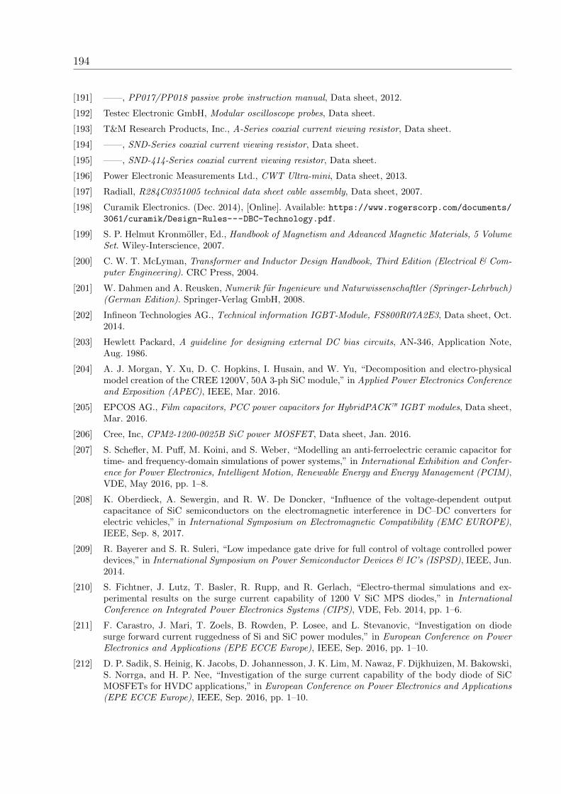
194
[191] ——, PP017/PP018 passive probe instruction manual, Data sheet, 2012.
[192] Testec Electronic GmbH, Modular oscilloscope probes, Data sheet.
[193] T&M Research Products, Inc., A-Series coaxial current viewing resistor, Data sheet.
[194] ——, SND-Series coaxial current viewing resistor, Data sheet.
[195] ——, SND-414-Series coaxial current viewing resistor, Data sheet.
[196] Power Electronic Measurements Ltd., CWT Ultra-mini, Data sheet, 2013.
[197] Radiall, R284C0351005 technical data sheet cable assembly, Data sheet, 2007.
[198] Curamik Electronics. (Dec. 2014), [Online]. Available: https://www.rogerscorp.com/documents/3061/curamik/Design-Rules---DBC-Technology.pdf.
[199] S. P. Helmut Kronmoller, Ed., Handbook of Magnetism and Advanced Magnetic Materials, 5 VolumeSet. Wiley-Interscience, 2007.
[200] C. W. T. McLyman, Transformer and Inductor Design Handbook, Third Edition (Electrical & Com-puter Engineering). CRC Press, 2004.
[201] W. Dahmen and A. Reusken, Numerik fur Ingenieure und Naturwissenschaftler (Springer-Lehrbuch)(German Edition). Springer-Verlag GmbH, 2008.
[202] Infineon Technologies AG., Technical information IGBT-Module, FS800R07A2E3, Data sheet, Oct.2014.
[203] Hewlett Packard, A guideline for designing external DC bias circuits, AN-346, Application Note,Aug. 1986.
[204] A. J. Morgan, Y. Xu, D. C. Hopkins, I. Husain, and W. Yu, “Decomposition and electro-physicalmodel creation of the CREE 1200V, 50A 3-ph SiC module,” in Applied Power Electronics Conferenceand Exposition (APEC), IEEE, Mar. 2016.
[205] EPCOS AG., Film capacitors, PCC power capacitors for HybridPACK™ IGBT modules, Data sheet,Mar. 2016.
[206] Cree, Inc, CPM2-1200-0025B SiC power MOSFET, Data sheet, Jan. 2016.
[207] S. Schefler, M. Puff, M. Koini, and S. Weber, “Modelling an anti-ferroelectric ceramic capacitor fortime- and frequency-domain simulations of power systems,” in International Exhibition and Confer-ence for Power Electronics, Intelligent Motion, Renewable Energy and Energy Management (PCIM),VDE, May 2016, pp. 1–8.
[208] K. Oberdieck, A. Sewergin, and R. W. De Doncker, “Influence of the voltage-dependent outputcapacitance of SiC semiconductors on the electromagnetic interference in DC–DC converters forelectric vehicles,” in International Symposium on Electromagnetic Compatibility (EMC EUROPE),IEEE, Sep. 8, 2017.
[209] R. Bayerer and S. R. Suleri, “Low impedance gate drive for full control of voltage controlled powerdevices,” in International Symposium on Power Semiconductor Devices & IC’s (ISPSD), IEEE, Jun.2014.
[210] S. Fichtner, J. Lutz, T. Basler, R. Rupp, and R. Gerlach, “Electro-thermal simulations and ex-perimental results on the surge current capability of 1200 V SiC MPS diodes,” in InternationalConference on Integrated Power Electronics Systems (CIPS), VDE, Feb. 2014, pp. 1–6.
[211] F. Carastro, J. Mari, T. Zoels, B. Rowden, P. Losee, and L. Stevanovic, “Investigation on diodesurge forward current ruggedness of Si and SiC power modules,” in European Conference on PowerElectronics and Applications (EPE ECCE Europe), IEEE, Sep. 2016, pp. 1–10.
[212] D. P. Sadik, S. Heinig, K. Jacobs, D. Johannesson, J. K. Lim, M. Nawaz, F. Dijkhuizen, M. Bakowski,S. Norrga, and H. P. Nee, “Investigation of the surge current capability of the body diode of SiCMOSFETs for HVDC applications,” in European Conference on Power Electronics and Applications(EPE ECCE Europe), IEEE, Sep. 2016, pp. 1–10.

Bibliography 195
[213] T. Basler, J. Lutz, R. Jakob, and T. Bruckner, “Surge current capability of IGBTs,” in InternationalMulti-Conference on Systems, Sygnals & Devices, IEEE, Mar. 2012, pp. 1–6.
[214] V. Banu, M. Berthou, J. Montserrat, X. Jorda, and P. Godignon, “Impact of layout on the surgecurrent robustness of 1.2 kV SiC diodes,” in International Semiconductor Conference (CAS), IEEE,Oct. 2017, pp. 147–150.
[215] R. Rupp, M. Treu, S. Voss, F. Bjork, and T. Reimann, “2nd generation SiC schottky diodes: A newbenchmark in SiC device ruggedness,” in International Symposium on Power Semiconductor Devicesand IC’s (ISPSD), IEEE, Jun. 2006, pp. 1–4.
[216] F. Cappelluti, F. Bonani, and G. Ghione, “Assessment of surge current capabilities of SiC-basedhigh-power diodes through physics-based mixed-mode electro-thermal simulations,” in InternationalSemiconductor Device Research Symposium, IEEE, Dec. 2009, pp. 1–2.
[217] M. Cenusa, G. Cretu, and M. Pfost, “An improved method of controlling IGBT modules usingan optimized gate current waveform,” in International Conference on Integrated Power ElectronicsSystems (CIPS), VDE, Feb. 2014, pp. 1–6.
[218] Cree, Inc, CPM2-1200-0040B SiC power MOSFET, Data sheet, Oct. 2016.
[219] Teledyne LeCroy, HDO6000 high definition oscilloscopes, Operator’s manual, Data sheet, Nov. 2013.

196

Aachener Beiträge des ISEA
ABISEA Band 1 Eßer, A. Berührungslose, kombinierte Energie- und Informations-übertragung für bewegliche Systeme 1. Auflage 1992, 130 Seiten ISBN 3-86073-046-0 ABISEA Band 2 Vogel, U. Entwurf und Beurteilung von Verfahren zur Hochausnutzung des Rad-Schiene-Kraftschlusses durch Triebfahrzeuge 1. Auflage 1992, 130 Seiten ISBN 3-86073-060-6 ABISEA Band 3 Redehorn, Th. Stromeinprägendes Antriebssystem mit fremderregter Synchron-maschine 1. Auflage 1992, 130 Seiten ISBN 3-86073-061-4 ABISEA Band 4 Ackva, A. Spannungseinprägendes Antriebssystem mit Synchron-maschine und direkter Stromregelung 1. Auflage 1992, 135 Seiten ISBN 3-86073-062-2 ABISEA Band 5 Mertens, A. Analyse des Oberschwingungsverhaltens von taktsynchronen Delta -Modulationsverfahren zur Steuerung von Pulsstromrichtern bei hoher Taktzahl 1. Auflage 1992, 170 Seiten ISBN 3-86073-069-X ABISEA Band 6 Geuer, W. Untersuchungen über das Alterungsverhalten von Bleiakkumulatoren 1. Auflage 1993, 100 Seiten ISBN 3-86073-097-5
ABISEA Band 7 Langheim, J. Einzelradantrieb für Elektrostraßenfahrzeuge 1. Auflage 1993, 215 Seiten ISBN 3-86073-123-8 (vergriffen) ABISEA Band 8 Fetz, J. Fehlertolerante Regelung eines Asynchron-Doppelantriebes für ein Elektrospeicherfahrzeug 1. Auflage 1993, 136 Seiten ISBN 3-86073-124-6 (vergriffen) ABISEA Band 9 Schülting, L. Optimierte Auslegung induktiver Bauelemente für den Mittelfrequenzbereich 1. Auflage 1993, 136 Seiten ISBN 3-86073-174-2 (vergriffen) ABISEA Band 10 Skudelny, H.-Ch. Stromrichtertechnik 4. Auflage 1997, 259 Seiten ISBN 3-86073-189-0 ABISEA Band 11 Skudelny, Ch. Elektrische Antriebe 3. Auflage 1997, 124 Seiten ISBN 3-86073-231-5 ABISEA Band 12 Schöpe, F. Batterie-Management für Nickel-Cadmium Akkumulatoren 1. Auflage 1994, 156 Seiten ISBN 3-86073-232-3 (vergriffen) ABISEA Band 13 v. d. Weem, J. Schmalbandige aktive Filter für Schienentriebfahrzeuge am Gleichspannungs-fahrdraht 1. Auflage 1995, 125 Seiten ISBN 3-86073-233-1
ABISEA Band 14 Backhaus, K. Spannungseinprägendes Direktantriebssystem mit schnelllaufender geschalteter Reluktanzmaschine 1. Auflage 1995, 156 Seiten ISBN 3-86073-234-X (vergriffen) ABISEA Band 15 Reinold, H. Optimierung dreiphasiger Pulsdauermodulations- verfahren 1. Auflage 1996, 116 Seiten ISBN 3-86073-235-8 ABISEA Band 16 Köpken, H.-G. Regelverfahren für Parallelschwingkreis- umrichter 1. Auflage 1996, 125 Seiten ISBN 3-86073-236-6 ABISEA Band 17 Mauracher, P. Modellbildung und Verbundoptimierung bei Elektrostraßenfahrzeugen 1. Auflage 1996, 192 Seiten ISBN 3-86073-237-4 ABISEA Band 18 Protiwa, F.-F. Vergleich dreiphasiger Resonanz-Wechselrichter in Simulation und Messung 1. Auflage 1997, 178 Seiten ISBN 3-86073-238-2 ABISEA Band 19 Brockmeyer, A. Dimensionierungswerkzeug für magnetische Bau- elemente in Stromrichter-anwendungen 1. Auflage 1997, 182 Seiten ISBN 3-86073-239-0 ABISEA Band 20 Apeldoorn, 0. Simulationsgestützte Bewer-tung von Steuerverfahren für netzgeführte Stromrichter mit verringerter Netzrück-wirkung 1. Auflage 1997, 132 Seiten ISBN 3-86073-680-9

Aachener Beiträge des ISEA
ABISEA Band 21 Lohner, A. Batteriemanagement für verschlossene Blei-Batterien am Beispiel von Unter-brechungsfreien Stromversorgungen 1. Auflage 1998, 144 Seiten ISBN 3-86073-681-7 ABISEA Band 22 Reinert, J. Optimierung der Betriebs-eigenschaften von Antrieben mit geschalteter Reluktanz-maschine 1. Auflage 1998, 168 Seiten ISBN 3-86073-682-5 ABISEA Band 23 Nagel, A. Leitungsgebundene Störungen in der Leistungselektronik: Entstehung, Ausbreitung und Filterung 1. Auflage 1999, 160 Seiten ISBN 3-86073-683-3 ABISEA Band 24 Menne, M. Drehschwingungen im An-triebsstrang von Elektro-straßenfahrzeugen - Analyse und aktive Dämpfung 1. Auflage 2001, 192 Seiten ISBN 3-86073-684-1 ABISEA Band 25 von Bloh, J. Multilevel-Umrichter zum Einsatz in Mittelspannungs-Gleichspannungs-Übertragungen 1. Auflage 2001, 152 Seiten ISBN 3-86073-685-X ABISEA Band 26 Karden, E. Using low-frequency impedance spectroscopy for characterization, monitoring, and modeling of industrial batteries 1. Auflage 2002, 154 Seiten ISBN 3-8265-9766-4
ABISEA Band 27 Karipidis, C.-U. A Versatile DSP/ FPGA Structure optimized for Rapid Prototyping and Digital Real-Time Simulation of Power Electronic and Electrical Drive Systems 1. Auflage 2001, 164 Seiten ISBN 3-8265-9738-9 ABISEA Band 28 Kahlen, K. Regelungsstrategien für per-manentmagnetische Direkt-antriebe mit mehreren Freiheitsgraden 1. Auflage 2003, 158 Seiten ISBN 3-8322-1222-1 ABISEA Band 29 Inderka, R. Direkte Drehmoment-regelung Geschalteter Reluktanzantriebe 1. Auflage 2003, 190 Seiten ISBN 3-8322-1175-6 ABISEA Band 30 Schröder, S. Circuit-Simulation Models of High-Power Devices Based on Semiconductor Physics 1. Auflage 2003, 124 Seiten ISBN 3-8322-1250-7 ABISEA Band 31 Buller, S. Impedance-Based Simu-lation Models for Energy Storage Devices in Advanced Automotive Power Systems 1. Auflage 2003, 136 Seiten ISBN 3-8322-1225-6 ABISEA Band 32 Schönknecht, A. Topologien und Regelungs-strategien für das induktive Erwärmen mit hohen Frequenz-Leistungs- produkten 1. Auflage 2004, 170 Seiten ISBN 3-8322-2408-4
ABISEA Band 33 Tolle, T. Konvertertopologien für ein aufwandsarmes, zwei-stufiges Schaltnetzteil zum Laden von Batterien aus dem Netz 1. Auflage 2004, 150 Seiten ISBN 3-8322-2676-1 ABISEA Band 34 Götting, G. Dynamische Antriebs-regelung von Elektro-straßenfahrzeugen unter Berücksichtigung eines schwingungsfähigen Antriebsstrangs 1. Auflage 2004, 166 Seiten ISBN 3-8322-2804-7 ABISEA Band 35 Dieckerhoff, S. Transformatorlose Strom-richterschaltungen für Bahn- fahrzeuge am 16 2/3Hz Netz 1. Auflage 2004, 158 Seiten ISBN 3-8322-3094-7 ABISEA Band 36 Hu, J. Bewertung von DC-DC- Topologien und Optimierung eines DC-DC-Leistungs-moduls für das 42-V-Kfz-Bordnetz 1. Auflage 2004, 156 Seiten ISBN 3-8322-3201-X ABISEA Band 37 Detjen, D.-0. Characterization and Modeling of Si-Si Bonded Hydrophobie Interfaces for Novel High-Power BIMOS Devices 1. Auflage 2004, 146 Seiten ISBN 3-8322-2963-9 ABISEA Band 38 Walter, J. Simulationsbasierte Zuver-lässigkeitsanalyse in der modernen Leistungs-elektronik 1. Auflage 2004, 134 Seiten ISBN 3-8322-3481-0

Aachener Beiträge des ISEA
ABISEA Band 39 Schwarzer, U. IGBT versus GCT in der Mittelspannungsanwendung - ein experimenteller und simulativer Vergleich 1. Auflage 2005, 184 Seiten ISBN 3-8322-4489-1 ABISEA Band 40 Bartram, M. IGBT-Umrichtersysteme für Windkraftanlagen: Analyse der Zyklenbelastung, Mo-dellbildung, Optimierung und Lebensdauervorhersage 1. Auflage 2006, 195 Seiten ISBN 3-8322-5039-5 ABISEA Band 41 Ponnaluri, S. Generalized Design, Analysis and Control of Grid side converters with integrated UPS or Islanding functionality 1. Auflage 2006, 163 Seiten ISBN 3-8322-5281-9 ABISEA Band 42 Jacobs, J. Multi-Phase Series Resonant DC-to-DC Converters 1. Auflage 2006, 185 Seiten ISBN 3-8322-5532-X ABISEA Band 43 Linzen, D. Impedance-Based Loss Calculation and Thermal Modeling of Electrochemical Energy Storage Devices for Design Considerations of Automotive Power Systems 1. Auflage 2006, 150 Seiten ISBN 3-8322-5706-3 ABISEA Band 44 Fiedler, J. Design of Low-Noise Switched Reluctance Drives 1. Auflage 2007, 183 Seiten ISBN 978-3-8322-5864-l
ABISEA Band 45 FuengwarodsakuI, N. Predictive PWM-based Direct Instantaneous Torque Control for Switched Reluctance Machines 1. Auflage 2007, 150 Seiten ISBN 978-3-8322-6210-5 ABISEA Band 46 Meyer, C. Key Components for Future Offshore DC Grids 1. Auflage 2007, 196 Seiten ISBN 978-3-8322-6571-7 ABISEA Band 47 Fujii, K. Characterization and Optimization of Soft-Switched Multi-Level Converters for STATCOMs 1. Auflage 2008, 206 Seiten ISBN 978-3-8322-6981-4 ABISEA Band 48 Carstensen, C. Eddy Currents in Windings of Switched Reluctance Machines 1. Auflage 2008, 190 Seiten ISBN 978-3-8322-7118-3 ABISEA Band 49 Bohlen, 0. Impedance-based battery monitoring 1. Auflage 2008, 200 Seiten ISBN 978-3-8322-7606-5 ABISEA Band 50 Thele, M. A contribution to the modelling of the charge acceptance of lead-acid batteries - using frequency and time domain based concepts 1. Auflage 2008, 168 Seiten ISBN 978-3-8322-7659-1 ABISEA Band 51 König, A. High Temperature DC-to-DC Converters for Downhole Applications 1. Auflage 2009, 160 Seiten ISBN 978-3-8322-8489-3
ABISEA Band 52 Dick, C. P. Multi-Resonant Converters as Photovoltaic Module-Integrated Maximum Power Point Tracker 1. Auflage 2010, 192 Seiten ISBN 978-3-8322-9199-0 ABISEA Band 53 Kowal, J. Spatially-resolved impedance of nonlinear inhomogeneous devices - using the example of lead-acid batteries - 1. Auflage 2010, 214 Seiten ISBN 978-3-8322-9483-0 ABISEA Band 54 Roscher, M. Zustandserkennung von LiFeP04-Batterien für Hybrid- und Elektrofahrzeuge 1. Auflage 2011, 194 Seiten ISBN 978-3-8322-9738-l ABISEA Band 55 Hirschmann, D. Highly Dynamic Piezoelectric Positioning 1. Auflage 2011, 156 Seiten ISBN 978-3-8322-9746-6 ABISEA Band 56 Rigbers, K. Highly Efficient Inverter Architectures for Three-Phase Grid Connection of Photovoltaic Generators 1. Auflage 2011, 254 Seiten ISBN 978-3-8322-9816-9 ABISEA Band 57 Kasper, K. Analysis and Control of the Acoustic Behavior of Switched Reluctance Drives 1. Auflage 2011, 214 Seiten ISBN 978-3-8322-9869-2 ABISEA Band 58 Köllensperger, P. The Internally Commutated Thyristor - Concept, Design and Application 1. Auflage 201 J, 212 Seiten ISBN 978-3-8322-9909-5

Aachener Beiträge des ISEA
ABISEA Band 59 Schoenen, T. Einsatz eines DC/DC-Wand-lers zur Spannungs-anpassung zwischen Antrieb und Energiespeicher in Elektro-und Hybrid-fahrzeugen 1. Auflage 2011, 138 Seiten ISBN 978-3-8440-0622-3 ABISEA Band 60 Hennen, M. Switched Reluctance Direct Drive with Integrated Distributed Inverter 1. Auflage 2012, 150 Seiten ISBN 978-3-8440-0731-2 ABISEA Band 61 van Treek, D. Position Sensorless Torque Control of Switched Reluctance Machines 1. Auflage 2012, 144 Seiten ISBN 978-3-8440-IO 14-5 ABISEA Band 62 Bragard, M. Tue Integrated Emitter Turn-Off Thyristor. An Innovative MOS-Gated High-Power Device 1. Auflage 2012, 172 Seiten ISBN 978-3-8440-1152-4 ABISEA Band 63 Gerschler, J. B. Ortsaufgelöste Modellbil-dung von Lithium-Ionen-Systemen unter spezieller Berücksichtigung der Batteriealterung 1. Auflage 2012, 350 Seiten ISBN 978-3-8440-1307-8 ABISEA Band 64 Neuhaus, C. Schaltstrategien für Geschaltete Reluktanz-antriebe mit kleinem Zwischenkreis 1. Auflage 2012, 144 Seiten ISBN 978-3-8440-1487-7
ABISEA Band 65 Butschen, T. Dual-ICT- A Clever Way to Unite Conduction and Switching Optimized Properties in a Single Wafer 1. Auflage 2012, 178 Seiten ISBN 978-3-8440-1771-7 ABISEA Band 66 Plum, T. Design and Realization of High-Power MOS Turn-Off Thyristors 1. Auflage 2013, 130 Seiten ISBN 978-3-8440-1884-4 ABISEA Band 67 Kiel, M. Impedanzspektroskopie an Batterien unter besonderer Berücksichtigung von Batteriesensoren für den Feldeinsatz 1. Auflage 2013, 232 Seiten ISBN 978-3-8440-1973-5 ABISEA Band 68 Brauer, H. Schnelldrehender Geschalteter Reluktanz-antrieb mit extremem Längendurchmesser-verhältnis 1. Auflage 2013, 202 Seiten ISBN 978-3-8440-2345-9 ABISEA Band 69 Thomas, S. A Medium-Voltage Multi-Level DC/DC Converter with High Voltage Transformation Ratio 1. Auflage 2014, 236 Seiten ISBN 978-3-8440-2605-4 ABISEA Band 70 Richter, S. Digitale Regelung von PWM Wechselrichtern mit niedrigen Trägerfrequenzen 1. Auflage 2014, 134 Seiten ISBN 978-3-8440-2641-2
ABISEA Band 71 Bösing, M. Acoustic Modeling of Electrical Drives - Noise and Vibration Synthesis based on Force Response Superposition 1. Auflage 2014, 208 Seiten ISBN 978-3-8440-2752-5 ABISEA Band 72 Waag, W. Adaptive algorithms for monitoring of lithium-ion batteries in electric vehicles 1. Auflage 2014, 242 Seiten ISBN 978-3-8440-2976-5 ABISEA Band 73 Sanders, T. Spatially Resolved Electrical In-Situ Measurement Techniques for Fuel Cells 1. Auflage 2014, 138 Seiten ISBN 978-3-8440-3121-8 ABISEA Band 74 Baumhöfer, T. Statistische Betrachtung experimenteller Alterungs-untersuchungen an Lithium-Ionen Batterien 1. Auflage 2015, 174 Seiten ISBN 978-3-8440-3423-3 ABISEA Band 75 Andre, D. Systematic Characterization of Ageing Factors for High- Energy Lithium-Ion Cells and Approaches for Lifetime Modelling Regarding an Optimized Operating Strategy in Automotive Applications 1. Auflage 2015, 210 Seiten ISBN 978-3-8440-3587-2 ABISEA Band 76 Merei, G. Optimization of off-grid hybrid PV-wind-diesel power supplies with multi-technology battery systems taking into account battery aging 1. Auflage 2015, 194 Seiten ISBN 978-3-8440-4148-4

Aachener Beiträge des ISEA
ABISEA Band 77 Schulte, D. Modellierung und experi-mentelle Validierung der Alterung von Blei-Säure Batterien durch inhomogene Stromverteilung und Säureschichtung 1. Auflage 2016, 168 Seiten ISBN 978-3-8440-4216-0 ABISEA Band 78 Schenk, M. Simulative Untersuchung der Wicklungsverluste in Geschalteten Reluktanz-maschinen 1. Auflage 2016, 142 Seiten ISBN 978-3-8440-4282-5 ABISEA Band 79 Wang, Y. Development of Dynamic Models with Spatial Resolution for Electro- chemical Energy Converters as Basis for Control and Management Strategies 1. Auflage 2016, 198 Seiten ISBN 978-3-8440-4303-7 ABISEA Band 80 Ecker, M. Lithium Plating in Lithium-Ion Batteries: An Experimental and Simulation Approach 1. Auflage 2016, 170 Seiten ISBN 978-3-8440-4525-3 ABISEA Band 81 Zhou, W. Modellbasierte Auslegungs-methode von Tempe-rierungssystemen für Hochvolt-Batterien in Personenkraftfahrzeugen 1. Auflage 2016, 192 Seiten ISBN 978-3-8440-4589-5 ABISEA Band 82 Lunz, B. Deutschlands Stromversor-gung im Jahr 2050 Ein szenariobasiertes Verfahren zur vergleich-enden Bewertung von Systemvarianten und Flexibilitätsoptionen 1. Auflage 2016, 196 Seiten ISBN 978-3-8440-4627-4
ABISEA Band 83 Hofmann, A. Direct Instantaneous Force Control Key to Low-Noise Switched Reluctance Traction Drives 1. Auflage 2016, 244 Seiten ISBN 978-3-8440-4715-8 ABISEA Band 84 Budde-Meiwes, H. Dynamic Charge Acceptance of Lead-Acid Batteries for Micro-Hybrid Automotive Applications 1. Auflage 2016, 168 Seiten ISBN 978-3-8440-4733-2 ABISEA Band 85 EngeI, S. P. Thyristor-Based High-Power On-Load Tap Changers Control under Harsh Load Conditions 1. Auflage 2016, 170 Seiten ISBN 978-3-8440-4986-2 ABISEA Band 86 VanHoek, H. Design and Operation Considerations of Three-Phase Dual Active Bridge Converters for Low-Power Applications with Wide Voltage Ranges 1. Auflage 2017, 242 Seiten ISBN 978-3-8440-5011-0 ABISEA Band 87 Diekhans, T. Wireless Charging of Electric Vehicles - a Pareto-Based Comparison of Power Electronic Topologies 1. Auflage 2017, 156 Seiten ISBN 978-3-8440-5048-6 ABISEA Band 88 Lehner, S. Reliability Assessment of Lithium-Ion Battery Systems with Special Emphasis on Cell Performance Distribution 1. Auflage 2017, 202 Seiten ISBN 978-3-8440-5090-5
ABISEA Band 89 Käbitz, S. Untersuchung der Alterung von Lithium-Ionen-Batterien mittels Elektroanalytik und elektrochemischer Impedanzspektroskopie 1. Auflage 2016, 258 Seiten DOI: 10.18154/RWTH-2016-12094 ABISEA Band 90 Witzenhausen, H. Elektrische Batteriespeichermodelle: Modellbildung, Parameteridentifikation und Modellreduktion 1. Auflage 2017, 286 Seiten DOI: 10.18154/RWTH-2017-03437 ABISEA Band 91 Münnix, J. Einfluss von Stromstärke und Zyklentiefe auf graphitische Anoden 1. Auflage 2017, 178 Seiten DOI: 10.18154/RWTH-2017- 01915 ABISEA Band 92 Pilatowicz, G. Failure Detection and Battery Management Systems of Lead-Acid Batteries for Micro- Hybrid Vehicles 1. Auflage 2017, 212 Seiten DOI: 10.18154/RWTH-2017-09156 ABISEA Band 93 Drillkens, J. Aging in Electrochemical Double Layer Capacitors: An Experimental and Modeling Approach 1. Aufl. 2017, 179 Seiten DOI: 10.18154/RWTH-2018-223434 ABISEA Band 94 Magnor, D. Globale Optimierung netz-gekoppelter PV-Batterie-systeme unter besonderer Berücksichtigung der Batteriealterung 1. Auflage 2017, 210 Seiten DOI: 10.18154/RWTH-2017-06592

Aachener Beiträge des ISEA
ABISEA Band 95 Iliksu, M. Elucidation and Comparison of the Effects of Lithium Salts on Discharge Chemistry of Nonaqueous Li-O2 Batteries 1. Aufl. 2018, 160 Seiten DOI: 10.18154/RWTH-2018-223782 ABISEA Band 96 Schmalstieg, J. Physikalisch-elektrochemische Simulation von Lithium- Ionen-Batterien: Implementierung, Parametrierung und Anwendung 1. Aufl. 2017, 176 Seiten DOI: 10.18154/RWTH-2017- 04693 ABISEA Band 97 Soltau, N. High-Power Medium-Voltage DC-DC Converters: Design, Control and Demonstration 1. Aufl. 2017, 176 Seiten DOI: 10.18154/RWTH-2017-04084 ABISEA Band 98 Stieneker, M. Analysis of Medium-Voltage Direct-Current Collector Grids in Offshore Wind Parks 1. Aufl. 2017, 144 Seiten DOI: 10.18154/RWTH-2017-04667 ABISEA Band 99 Masomtob, M. A New Conceptual Design of Battery Cell with an Internal Cooling Channel 1. Aufl. 2017, 167 Seiten DOI: 10.18154/RWTH-2018-223281 ABISEA Band 100 Marongiu, A. Performance and Aging Diagnostic on Lithium Iron Phosphate Batteries for Electric Vehicles and Vehicle-to-Grid Strategies 1. Aufl. 2017, 222 Seiten
DOI: 10.18154/RWTH-2017-09944 ABISEA Band 101 Gitis, A. Flaw detection in the coating process of lithium-ion battery electrodes with acoustic guided waves 1. Aufl. 2017, 132 Seiten DOI: 10.18154/RWTH-2017-099519 ABISEA Band 102 Neeb, C. Packaging Technologies for Power Electronics in Automotive Applications 1. Aufl. 2017, 132 Seiten DOI: 10.18154/RWTH-2018-224569 ABISEA Band 103 Adler, F. S. A Digital Hardware Platform for Distributed Real-Time Simulation of Power Electronic Systems 1. Aufl. 2017, 156 Seiten DOI: 10.18154/RWTH-2017-10761 ABISEA Band 104 Becker, J. Flexible Dimensionierung und Optimierung hybrider Lithium-Ionenbatteriespeichersysteme mit verschiedenen Auslegungszielen 1. Aufl., 2017, 157 Seiten DOI: 10.18154/RWTH-2017-09278 ABISEA Band 105 Warnecke, A. Degradation Mechanisms in NMC Based Lithium-Ion Batteries 1. Aufl. 2017, 158 Seiten DOI: 10.18154/RWTH-2017-09646 ABISEA Band 106 Taraborrelli, S. Bidirectional Dual Active Bridge Converter using a Tap Changer for Extended Voltage Ranges 1. Aufl. 2017
ABISEA Band 107 Sarriegi, G. SiC and GaN Semiconductors – The Future Enablers of Compact and Efficient Converters for Electromobility 1. Aufl. 2017 ABISEA Band 108 Senol, M. Drivetrain Integrated Dc-Dc Converters utilizing Zero Sequence Currents 1. Aufl. 2017 ABISEA Band 109 Koijma, T. Efficiency Optimized Control of Switched Reluctance Machines 1. Aufl. 2017 ABISEA Band 110 Lewerenz, M. Dissection and Quantitative Description of Aging of Lithium-Ion Batteries Using Non-Destructive Methods Validated by Post-Mortem-Analyses 1. Aufl. 2018 ABISEA Band 111 Büngeler, J. Optimierung der Verfüg-barkeit und der Lebens-dauer von Traktionsbatterien für den Einsatz in Flurförder-fahrzeugen 1. Aufl. 2018 ABISEA Band 112 Wegmann, R. Betriebsstrategien und Potentialbewertung hybrider Batteriespeichersysteme in Elektrofahrzeugen 1. Auflage 2018 ABISEA Band 113 Nordmann, H. Batteriemanagementsysteme unter besonderer Berück-sichtigung von Fehlererken-nung und Peripherieanalyse 1. Aufl. 2018

ISSN 1437-675X
The aims of this thesis are to investigate the influence of the packages and the driving circuits on the switching behavior of Si IGBTs and SiC MOSFETs. The peak voltages and surge cur-rents during switching determine the stress on the devices. The stress depends on several parasitic elements in and around the switching cell and the gate driving circuitry.
First, different techniques to identify and parametrize inducti-ve and capacitive parasitics of the packages are shown. The presented concepts are demonstrated using representative packages for a wide range of different power electronics pa-ckages. In a second step, the influence of the different parasitic inductive elements on the switching transients is investigated using a switching cell with variable inductive elements. The im-pact of each inductive element on the switching behavior is in-vestigated regarding the stress on the device and the resulting switching losses. Third, to influence the switching behavior of the device, a switched resistor, stage-wise gate driver is desig-ned for a Si IGBT power module and a SiC MOSFET switching cell. It is shown that the switching transients can be manipula-ted to balance device stresses and switching losses.
The use of active gate drivers shows that it is possible to reduce the stress on the device in addition to the impact of the swit-ching cell design. It is shown in this thesis, that the switching performance can be further improved for power semiconductors in packages that are electrically not optimal, due to third-party design and production constraints.