Analysis of Power Switching Losses Accounting Probe Modeling
9
3218 IEEE TRANSACTIONS ON INSTRUMENTATION AND MEASUREMENT, VOL. 59, NO. 12, DECEMBER 2010 Analysis of Power Switching Losses Accounting Probe Modeling Kaiçar Ammous, Hervé Morel, Student Member, IEEE, and Anis Ammous Abstract—This paper focuses on the errors affecting the esti- mation of power switching losses in power semiconductor devices based on integration of the voltage by current product. It is shown that the measured waveforms are not simply delayed by the probes, but some overshoots and distortions are due to the probes, which may not easily be corrected. These effects are the source of errors, particularly in fast transients. This paper shows analyses of simulation and measurements, including probe models. Index Terms—Distortions, losses, measurement, power, probe modeling. I. I NTRODUCTION O NE CLASSICAL approach for the estimation of switch- ing losses in a power semiconductor device is based on the calculation of the power signal as the product of the current by the voltage signals. Then, the power signal is integrated. For medium power range devices, the transients may occur in some tens of nanoseconds. Recent papers [1], [2] have addressed the measurement of semiconductor device losses and focused on the limitations of digital oscilloscopes and their calibration with respect to high-speed waveforms. Other papers addressed the power loss measurement in the case of microwave power ampli- fiers [3], [4], where the power amplifiers are integrated circuits for which probes cannot be inserted. The present problem of loss measurements is then different. Current and voltage probes are inserted inside the circuit and connected to an oscilloscope. To avoid boundary effect perturbations, a good practice is to measure signals on a device connected near the ground of the circuit or any other constant potential of the circuit. As the frequency bandwidth is a key parameter in such a measurement system, it is assumed that the current and voltage probes, as well as the oscilloscope, have a sufficient bandwidth. Moreover, the probe is considered linear. Application notes [5]–[8] point out that the instrumentation system should exceed this bandwidth by a factor of 3. This paper presents the analysis of probe effects on waveform measurements of a diode component during fast switching phases. Manuscript received November 20, 2009; revised February 22, 2010; accepted February 23, 2010. Date of publication September 2, 2010; date of current version November 10, 2010. K. Ammous and A. Ammous are with the Groupe de Recherche, Power Electronic Group, Département de Génie Electrique, Ecole Nationale d’Ingénieurs de Sfax, 3038 Sfax, Tunisia (e-mail: [email protected]; [email protected]). H. Morel is with the Universite de Lyon, INSA-Lyon, Lab. AMPERE, CNRS #5005, 69621 Villeurbanne, France. Color versions of one or more of the figures in this paper are available online at http://ieeexplore.ieee.org. Digital Object Identifier 10.1109/TIM.2010.2047302 This paper also focuses on probe modeling and compares simulation results with measurement results on a switching cell. Following the introduction, this paper is organized in three additional sections. Section II presents probe and cable length effects on signal delays in a simple test circuit. Section III introduces refined models of the probes and describes a test circuit (a switching cell) that is used to measure the current and voltage waveforms of a power diode device under test (DUT) to illustrate how the probes affect the waveform measurements. Section IV presents results on power diode turnoff. II. TEST CIRCUIT TO ESTIMATE DELAY The simple test circuit in Fig. 1 is considered to show the delay introduced by the current and voltage probes. Capacitor C is used to supply to transient currents, and the current source includes a serial self-inductor to avoid transient voltages. V R is a voltage source, and I F is a current source. It appears that synchronicity between waveforms is of prime importance (Figs. 1 and 2). Application notes [8] indicate that a delay correction is required, which may even be treated by high-quality oscilloscopes as a simple time skew (namely, the deskewing process). The delay depends on probe and cable lengths. A TMS-Research 1.2-GHz shunt [9] was used as the current probe, and a Tektronix P6139A 500-MHz voltage probe was considered. In Fig. 1, an IRF740 MOSFET tran- sistor creates a current step waveform inside a 50-Ω MP930 high-frequency resistor. Fig. 2 shows the current and voltage waveforms. A 3-ns delay may be estimated for 1 m of cable for both probes. However, Section III will show that a correction of the latter delay between current and voltage waveforms is not sufficient to guarantee an accurate estimation of power losses. Fig. 3 shows the current waveforms during switching phases obtained by different types of current probes at turnoff of a diode DUT. Each current waveform case corresponds to a shunt connected with a given type of cable. Two types of cables were used, namely, coaxial (with two different lengths) and rigid coaxial copper cables. Measurements show that the copper cable gives the lowest overshoots and, thus, a more accurate current waveform. Interactions also occur, and a good calibration of probes is required. Fig. 4 shows the classical equivalent circuit represent- ing the interaction between a voltage probe and an oscilloscope. The cable is considered as ideal. In the case of semiconductor devices of medium current range (1–30 A), the OFF-state ca- pacitance of the DUT is of the same order of magnitude as the voltage probe input capacitance (C t ≈ C s =8 pF, equivalent 0018-9456/$26.00 © 2010 IEEE
Transcript of Analysis of Power Switching Losses Accounting Probe Modeling
3218 IEEE TRANSACTIONS ON INSTRUMENTATION AND MEASUREMENT, VOL. 59, NO. 12, DECEMBER 2010
Analysis of Power Switching LossesAccounting Probe Modeling
Kaiçar Ammous, Hervé Morel, Student Member, IEEE, and Anis Ammous
Abstract—This paper focuses on the errors affecting the esti-mation of power switching losses in power semiconductor devicesbased on integration of the voltage by current product. It isshown that the measured waveforms are not simply delayed by theprobes, but some overshoots and distortions are due to the probes,which may not easily be corrected. These effects are the source oferrors, particularly in fast transients. This paper shows analysesof simulation and measurements, including probe models.
Index Terms—Distortions, losses, measurement, power, probemodeling.
I. INTRODUCTION
ONE CLASSICAL approach for the estimation of switch-ing losses in a power semiconductor device is based on
the calculation of the power signal as the product of the currentby the voltage signals. Then, the power signal is integrated. Formedium power range devices, the transients may occur in sometens of nanoseconds. Recent papers [1], [2] have addressed themeasurement of semiconductor device losses and focused onthe limitations of digital oscilloscopes and their calibration withrespect to high-speed waveforms. Other papers addressed thepower loss measurement in the case of microwave power ampli-fiers [3], [4], where the power amplifiers are integrated circuitsfor which probes cannot be inserted. The present problem ofloss measurements is then different. Current and voltage probesare inserted inside the circuit and connected to an oscilloscope.
To avoid boundary effect perturbations, a good practice is tomeasure signals on a device connected near the ground of thecircuit or any other constant potential of the circuit.
As the frequency bandwidth is a key parameter in such ameasurement system, it is assumed that the current and voltageprobes, as well as the oscilloscope, have a sufficient bandwidth.Moreover, the probe is considered linear.
Application notes [5]–[8] point out that the instrumentationsystem should exceed this bandwidth by a factor of 3.
This paper presents the analysis of probe effects on waveformmeasurements of a diode component during fast switchingphases.
Manuscript received November 20, 2009; revised February 22, 2010;accepted February 23, 2010. Date of publication September 2, 2010; date ofcurrent version November 10, 2010.
K. Ammous and A. Ammous are with the Groupe de Recherche,Power Electronic Group, Département de Génie Electrique, Ecole Nationaled’Ingénieurs de Sfax, 3038 Sfax, Tunisia (e-mail: [email protected];[email protected]).
H. Morel is with the Universite de Lyon, INSA-Lyon, Lab. AMPERE,CNRS #5005, 69621 Villeurbanne, France.
Color versions of one or more of the figures in this paper are available onlineat http://ieeexplore.ieee.org.
Digital Object Identifier 10.1109/TIM.2010.2047302
This paper also focuses on probe modeling and comparessimulation results with measurement results on a switching cell.
Following the introduction, this paper is organized in threeadditional sections. Section II presents probe and cable lengtheffects on signal delays in a simple test circuit. Section IIIintroduces refined models of the probes and describes a testcircuit (a switching cell) that is used to measure the current andvoltage waveforms of a power diode device under test (DUT)to illustrate how the probes affect the waveform measurements.Section IV presents results on power diode turnoff.
II. TEST CIRCUIT TO ESTIMATE DELAY
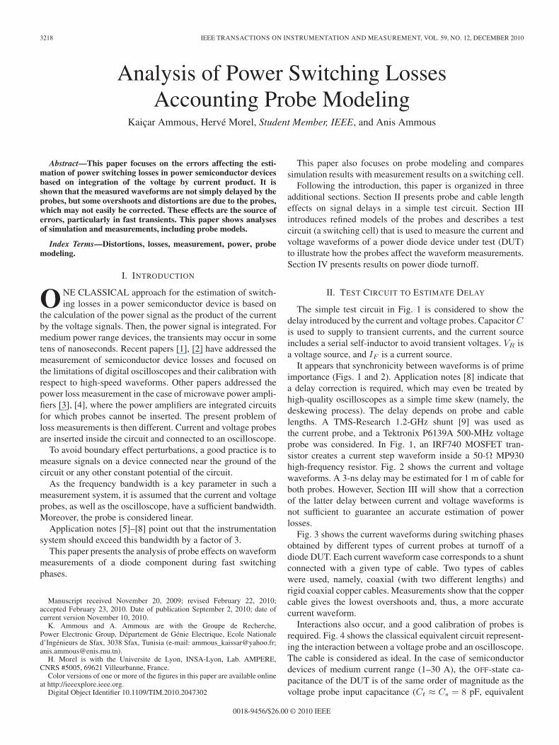
The simple test circuit in Fig. 1 is considered to show thedelay introduced by the current and voltage probes. Capacitor Cis used to supply to transient currents, and the current sourceincludes a serial self-inductor to avoid transient voltages. VR isa voltage source, and IF is a current source.
It appears that synchronicity between waveforms is of primeimportance (Figs. 1 and 2). Application notes [8] indicate thata delay correction is required, which may even be treated byhigh-quality oscilloscopes as a simple time skew (namely, thedeskewing process). The delay depends on probe and cablelengths. A TMS-Research 1.2-GHz shunt [9] was used asthe current probe, and a Tektronix P6139A 500-MHz voltageprobe was considered. In Fig. 1, an IRF740 MOSFET tran-sistor creates a current step waveform inside a 50-Ω MP930high-frequency resistor. Fig. 2 shows the current and voltagewaveforms. A 3-ns delay may be estimated for 1 m of cable forboth probes. However, Section III will show that a correctionof the latter delay between current and voltage waveforms isnot sufficient to guarantee an accurate estimation of powerlosses.
Fig. 3 shows the current waveforms during switching phasesobtained by different types of current probes at turnoff of adiode DUT. Each current waveform case corresponds to a shuntconnected with a given type of cable. Two types of cableswere used, namely, coaxial (with two different lengths) andrigid coaxial copper cables. Measurements show that the coppercable gives the lowest overshoots and, thus, a more accuratecurrent waveform.
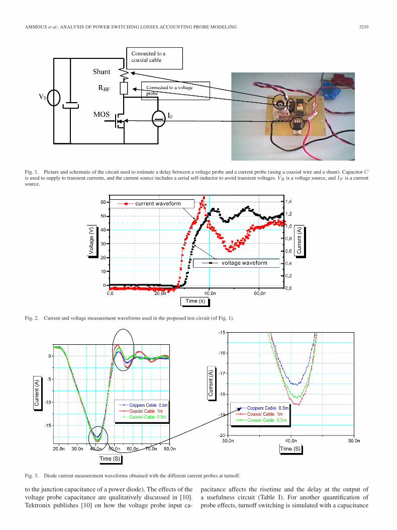
Interactions also occur, and a good calibration of probes isrequired. Fig. 4 shows the classical equivalent circuit represent-ing the interaction between a voltage probe and an oscilloscope.The cable is considered as ideal. In the case of semiconductordevices of medium current range (1–30 A), the OFF-state ca-pacitance of the DUT is of the same order of magnitude as thevoltage probe input capacitance (Ct ≈ Cs = 8 pF, equivalent
0018-9456/$26.00 © 2010 IEEE
AMMOUS et al.: ANALYSIS OF POWER SWITCHING LOSSES ACCOUNTING PROBE MODELING 3219
Fig. 1. Picture and schematic of the circuit used to estimate a delay between a voltage probe and a current probe (using a coaxial wire and a shunt). Capacitor Cis used to supply to transient currents, and the current source includes a serial self-inductor to avoid transient voltages. VR is a voltage source, and IF is a currentsource.
Fig. 2. Current and voltage measurement waveforms used in the proposed test circuit (of Fig. 1).
Fig. 3. Diode current measurement waveforms obtained with the different current probes at turnoff.
to the junction capacitance of a power diode). The effects of thevoltage probe capacitance are qualitatively discussed in [10].Tektronix publishes [10] on how the voltage probe input ca-
pacitance affects the risetime and the delay at the output ofa usefulness circuit (Table I). For another quantification ofprobe effects, turnoff switching is simulated with a capacitance
3220 IEEE TRANSACTIONS ON INSTRUMENTATION AND MEASUREMENT, VOL. 59, NO. 12, DECEMBER 2010
Fig. 4. Classical equivalent circuit representing the probe and the oscilloscopeinput.
TABLE IMEASUREMENT ERROR INTRODUCED INTO A CIRCUIT OUTPUT
SIGNAL BY THE INPUT CAPACITANCE OF THE PROBE
Fig. 5. Circuit used to simulate the diode under test behavior and the effect ofthe probe on current and voltage waveforms.
Fig. 6. Driving signals of the IGBT and the MOSFET used in the proposedtest circuit (of Fig. 5).
connecting in parallel with a diode DUT (Fig. 5). Drivingsignals of the insulated gate bipolar transistor (IGBT) and theMOSFET used in the proposed test circuit (Fig. 5) are shownin Fig. 6. Capacitor C represents the input capacitance of theprobes device. Fig. 7 pictures how capacitor C affects these
Fig. 7. Effect of the equivalent capacitance of the probe on diode current andvoltage parameters during turnoff.
latter parameters and power loss estimations in the diode. Toenlighten the errors in the estimation of power losses, one ideais to model the voltage and current probes and include thesedevices in the simulation process to improve the pertinence ofthe comparison between simulations and measurements. Often,in circuit simulations, the voltage probe is simply modeled as asimple equivalent circuit (Fig. 4), or it is not taken into accountat all. Indeed, probe devices are more complex and may bedescribed by the schematic in Fig. 8. It is well known that thevoltage probe has to be calibrated to ensure a constant ratiobetween input and output voltages over a wide frequency range.
Nevertheless, even if adequately calibrated, a voltage or acurrent probe introduces distortion on the waveform.
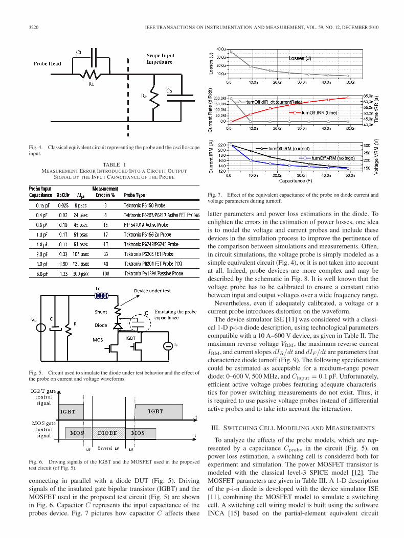
The device simulator ISE [11] was considered with a classi-cal 1-D p-i-n diode description, using technological parameterscompatible with a 10 A–600 V device, as given in Table II. Themaximum reverse voltage VRM, the maximum reverse currentIRM, and current slopes dIR/dt and dIF /dt are parameters thatcharacterize diode turnoff (Fig. 9). The following specificationscould be estimated as acceptable for a medium-range powerdiode: 0–600 V, 500 MHz, and Cinput = 0.1 pF. Unfortunately,efficient active voltage probes featuring adequate characteris-tics for power switching measurements do not exist. Thus, itis required to use passive voltage probes instead of differentialactive probes and to take into account the interaction.
III. SWITCHING CELL MODELING AND MEASUREMENTS
To analyze the effects of the probe models, which are rep-resented by a capacitance Cprobe in the circuit (Fig. 5), onpower loss estimation, a switching cell is considered both forexperiment and simulation. The power MOSFET transistor ismodeled with the classical level-3 SPICE model [12]. TheMOSFET parameters are given in Table III. A 1-D descriptionof the p-i-n diode is developed with the device simulator ISE[11], combining the MOSFET model to simulate a switchingcell. A switching cell wiring model is built using the softwareINCA [15] based on the partial-element equivalent circuit
AMMOUS et al.: ANALYSIS OF POWER SWITCHING LOSSES ACCOUNTING PROBE MODELING 3221
Fig. 8. Proposed model of the voltage probe: probe head model circuit CtRt, cable modeled by the sequence of line elements (R, L, G, C), probe bodyrepresented by Rbod and variable capacitance Cbod, and scope input impedance model circuit CsRs.
TABLE IIPARAMETER VALUES OBTAINED BY THE EXTRACTION PROCEDURE FOR DIODE AND MOSFET DEVICES
Fig. 9. Simulation waveforms of the voltage and the current evolution during turnoff [diode DUT BYT12PI1000, MOSFET IRF740, Lc = 90 nH (parasitic wireinductance), IF = 2 A, VR = 150 V, and T = 300 K]. t1 is the time where the current reaches zero, t2 is the time of the maximum current, t3 is the time of themaximum voltage, and t4 is the time where the voltage reaches VR.
(PEEC) method [14]. The next section describes the circuitoperating the switching cell under controlled conditions. Themost stressing transient phase is definitely when the power p-i-ndiode turns off. The power generated by the diode duringturnoff is taken as an example for discussing the probe behaviorand the interactions between the circuit and the probes.
The experimental setup is given in Fig. 5. It includes aswitching cell (MOSFET transistor and p-i-n diode), voltageVR, and current IF dc supplies, but the control electronicsis not shown. The MOSFET transistor (IRF740) ensures fastblocking of the diode current. The IGBT transistor (MUP304),which is slower but more robust than the MOSFET transistor,
3222 IEEE TRANSACTIONS ON INSTRUMENTATION AND MEASUREMENT, VOL. 59, NO. 12, DECEMBER 2010
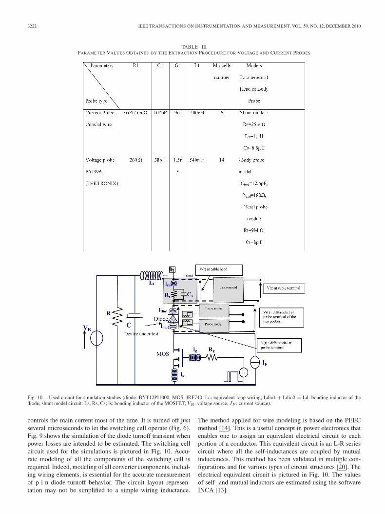
TABLE IIIPARAMETER VALUES OBTAINED BY THE EXTRACTION PROCEDURE FOR VOLTAGE AND CURRENT PROBES
Fig. 10. Used circuit for simulation studies (diode: BYT12PI1000; MOS: IRF740; Lc: equivalent loop wiring; Ldio1 + Ldio2 = Ld: bonding inductor of thediode; shunt model circuit: Ls, Rs, Cs; ls: bonding inductor of the MOSFET; VR: voltage source; IF : current source).
controls the main current most of the time. It is turned off justseveral microseconds to let the switching cell operate (Fig. 6).Fig. 9 shows the simulation of the diode turnoff transient whenpower losses are intended to be estimated. The switching cellcircuit used for the simulations is pictured in Fig. 10. Accu-rate modeling of all the components of the switching cell isrequired. Indeed, modeling of all converter components, includ-ing wiring elements, is essential for the accurate measurementof p-i-n diode turnoff behavior. The circuit layout represen-tation may not be simplified to a simple wiring inductance.
The method applied for wire modeling is based on the PEECmethod [14]. This is a useful concept in power electronics thatenables one to assign an equivalent electrical circuit to eachportion of a conductor. This equivalent circuit is an L-R seriescircuit where all the self-inductances are coupled by mutualinductances. This method has been validated in multiple con-figurations and for various types of circuit structures [20]. Theelectrical equivalent circuit is pictured in Fig. 10. The valuesof self- and mutual inductors are estimated using the softwareINCA [13].
AMMOUS et al.: ANALYSIS OF POWER SWITCHING LOSSES ACCOUNTING PROBE MODELING 3223
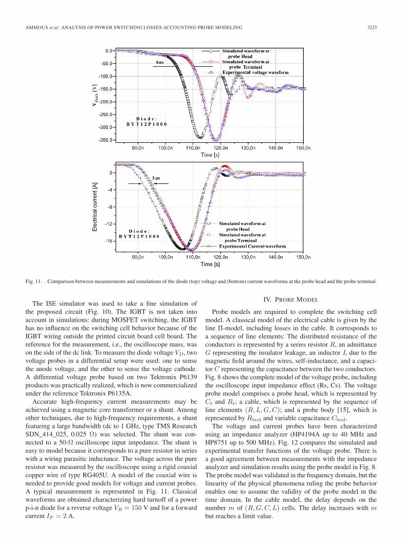
Fig. 11. Comparison between measurements and simulations of the diode (top) voltage and (bottom) current waveforms at the probe head and the probe terminal.
The ISE simulator was used to take a fine simulation ofthe proposed circuit (Fig. 10). The IGBT is not taken intoaccount in simulations: during MOSFET switching, the IGBThas no influence on the switching cell behavior because of theIGBT wiring outside the printed circuit board cell board. Thereference for the measurement, i.e., the oscilloscope mass, wason the side of the dc link. To measure the diode voltage VD, twovoltage probes in a differential setup were used: one to sensethe anode voltage, and the other to sense the voltage cathode.A differential voltage probe based on two Tektronix P6139products was practically realized, which is now commercializedunder the reference Tektronix P6135A.
Accurate high-frequency current measurements may beachieved using a magnetic core transformer or a shunt. Amongother techniques, due to high-frequency requirements, a shuntfeaturing a large bandwidth (dc to 1 GHz, type TMS ResearchSDN_414_025, 0.025 Ω) was selected. The shunt was con-nected to a 50-Ω oscilloscope input impedance. The shunt iseasy to model because it corresponds to a pure resistor in serieswith a wiring parasitic inductance. The voltage across the pureresistor was measured by the oscilloscope using a rigid coaxialcopper wire of type RG405U. A model of the coaxial wire isneeded to provide good models for voltage and current probes.A typical measurement is represented in Fig. 11. Classicalwaveforms are obtained characterizing hard turnoff of a powerp-i-n diode for a reverse voltage VR = 150 V and for a forwardcurrent IF = 2 A.
IV. PROBE MODEL
Probe models are required to complete the switching cellmodel. A classical model of the electrical cable is given by theline Π-model, including losses in the cable. It corresponds toa sequence of line elements: The distributed resistance of theconductors is represented by a series resistor R, an admittanceG representing the insulator leakage, an inductor L due to themagnetic field around the wires, self-inductance, and a capaci-tor C representing the capacitance between the two conductors.Fig. 8 shows the complete model of the voltage probe, includingthe oscilloscope input impedance effect (Rs, Cs). The voltageprobe model comprises a probe head, which is represented byCt and Rt; a cable, which is represented by the sequence ofline elements (R,L,G,C); and a probe body [15], which isrepresented by Rbod and variable capacitance Cbod.
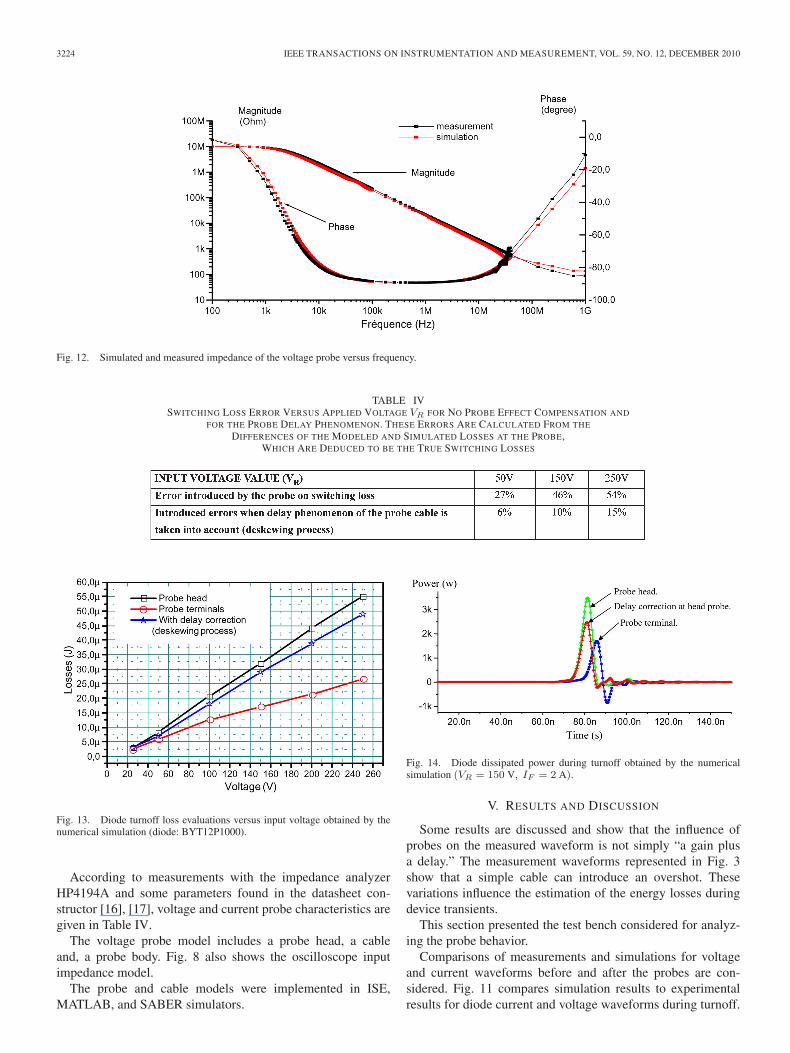
The voltage and current probes have been characterizedusing an impedance analyzer (HP4194A up to 40 MHz andHP8751 up to 500 MHz). Fig. 12 compares the simulated andexperimental transfer functions of the voltage probe. There isa good agreement between measurements with the impedanceanalyzer and simulation results using the probe model in Fig. 8.The probe model was validated in the frequency domain, but thelinearity of the physical phenomena ruling the probe behaviorenables one to assume the validity of the probe model in thetime domain. In the cable model, the delay depends on thenumber m of (R,G,C,L) cells. The delay increases with mbut reaches a limit value.
3224 IEEE TRANSACTIONS ON INSTRUMENTATION AND MEASUREMENT, VOL. 59, NO. 12, DECEMBER 2010
Fig. 12. Simulated and measured impedance of the voltage probe versus frequency.
TABLE IVSWITCHING LOSS ERROR VERSUS APPLIED VOLTAGE VR FOR NO PROBE EFFECT COMPENSATION AND
FOR THE PROBE DELAY PHENOMENON. THESE ERRORS ARE CALCULATED FROM THE
DIFFERENCES OF THE MODELED AND SIMULATED LOSSES AT THE PROBE,WHICH ARE DEDUCED TO BE THE TRUE SWITCHING LOSSES
Fig. 13. Diode turnoff loss evaluations versus input voltage obtained by thenumerical simulation (diode: BYT12P1000).
According to measurements with the impedance analyzerHP4194A and some parameters found in the datasheet con-structor [16], [17], voltage and current probe characteristics aregiven in Table IV.
The voltage probe model includes a probe head, a cableand, a probe body. Fig. 8 also shows the oscilloscope inputimpedance model.
The probe and cable models were implemented in ISE,MATLAB, and SABER simulators.
Fig. 14. Diode dissipated power during turnoff obtained by the numericalsimulation (VR = 150 V, IF = 2 A).
V. RESULTS AND DISCUSSION
Some results are discussed and show that the influence ofprobes on the measured waveform is not simply “a gain plusa delay.” The measurement waveforms represented in Fig. 3show that a simple cable can introduce an overshot. Thesevariations influence the estimation of the energy losses duringdevice transients.
This section presented the test bench considered for analyz-ing the probe behavior.
Comparisons of measurements and simulations for voltageand current waveforms before and after the probes are con-sidered. Fig. 11 compares simulation results to experimentalresults for diode current and voltage waveforms during turnoff.
AMMOUS et al.: ANALYSIS OF POWER SWITCHING LOSSES ACCOUNTING PROBE MODELING 3225
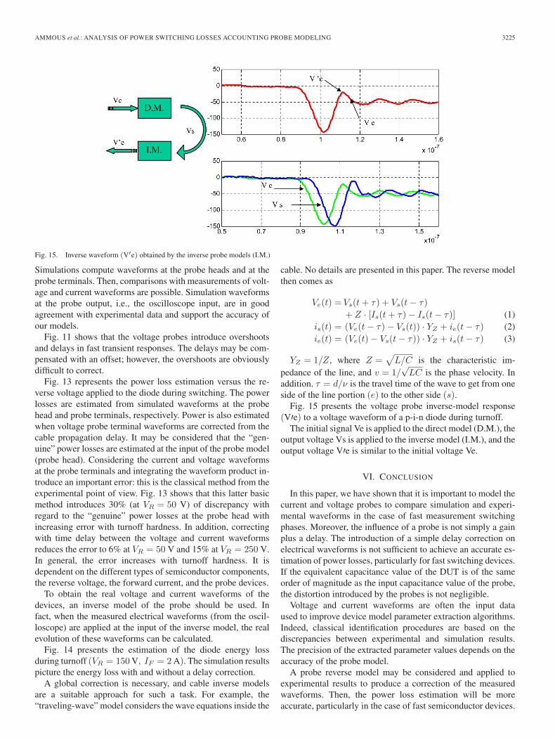
Fig. 15. Inverse waveform (V′e) obtained by the inverse probe models (I.M.)
Simulations compute waveforms at the probe heads and at theprobe terminals. Then, comparisons with measurements of volt-age and current waveforms are possible. Simulation waveformsat the probe output, i.e., the oscilloscope input, are in goodagreement with experimental data and support the accuracy ofour models.
Fig. 11 shows that the voltage probes introduce overshootsand delays in fast transient responses. The delays may be com-pensated with an offset; however, the overshoots are obviouslydifficult to correct.
Fig. 13 represents the power loss estimation versus the re-verse voltage applied to the diode during switching. The powerlosses are estimated from simulated waveforms at the probehead and probe terminals, respectively. Power is also estimatedwhen voltage probe terminal waveforms are corrected from thecable propagation delay. It may be considered that the “gen-uine” power losses are estimated at the input of the probe model(probe head). Considering the current and voltage waveformsat the probe terminals and integrating the waveform product in-troduce an important error: this is the classical method from theexperimental point of view. Fig. 13 shows that this latter basicmethod introduces 30% (at VR = 50 V) of discrepancy withregard to the “genuine” power losses at the probe head withincreasing error with turnoff hardness. In addition, correctingwith time delay between the voltage and current waveformsreduces the error to 6% at VR = 50 V and 15% at VR = 250 V.In general, the error increases with turnoff hardness. It isdependent on the different types of semiconductor components,the reverse voltage, the forward current, and the probe devices.
To obtain the real voltage and current waveforms of thedevices, an inverse model of the probe should be used. Infact, when the measured electrical waveforms (from the oscil-loscope) are applied at the input of the inverse model, the realevolution of these waveforms can be calculated.
Fig. 14 presents the estimation of the diode energy lossduring turnoff (VR = 150 V, IF = 2 A). The simulation resultspicture the energy loss with and without a delay correction.
A global correction is necessary, and cable inverse modelsare a suitable approach for such a task. For example, the“traveling-wave” model considers the wave equations inside the
cable. No details are presented in this paper. The reverse modelthen comes as
Ve(t) =Vs(t + τ) + Vs(t − τ)+ Z · [Is(t + τ) − Is(t − τ)] (1)
is(t) = (Ve(t − τ) − Vs(t)) · YZ + ie(t − τ) (2)ie(t) = (Ve(t) − Vs(t − τ)) · YZ + is(t − τ) (3)
YZ = 1/Z, where Z =√
L/C is the characteristic im-pedance of the line, and v = 1/
√LC is the phase velocity. In
addition. τ = d/ν is the travel time of the wave to get from oneside of the line portion (e) to the other side (s).
Fig. 15 presents the voltage probe inverse-model response(V′e) to a voltage waveform of a p-i-n diode during turnoff.
The initial signal Ve is applied to the direct model (D.M.), theoutput voltage Vs is applied to the inverse model (I.M.), and theoutput voltage V′e is similar to the initial voltage Ve.
VI. CONCLUSION
In this paper, we have shown that it is important to model thecurrent and voltage probes to compare simulation and experi-mental waveforms in the case of fast measurement switchingphases. Moreover, the influence of a probe is not simply a gainplus a delay. The introduction of a simple delay correction onelectrical waveforms is not sufficient to achieve an accurate es-timation of power losses, particularly for fast switching devices.If the equivalent capacitance value of the DUT is of the sameorder of magnitude as the input capacitance value of the probe,the distortion introduced by the probes is not negligible.
Voltage and current waveforms are often the input dataused to improve device model parameter extraction algorithms.Indeed, classical identification procedures are based on thediscrepancies between experimental and simulation results.The precision of the extracted parameter values depends on theaccuracy of the probe model.
A probe reverse model may be considered and applied toexperimental results to produce a correction of the measuredwaveforms. Then, the power loss estimation will be moreaccurate, particularly in the case of fast semiconductor devices.
3226 IEEE TRANSACTIONS ON INSTRUMENTATION AND MEASUREMENT, VOL. 59, NO. 12, DECEMBER 2010
REFERENCES
[1] Y. Lembeye, “Métrologie de La Commutation de Puissance Rapide.Contribution à la Caractérisation et à la Recherche d’un Model d’IGBT,”Ph.D. dissertation, I.N.P. de Grenoble, Grenoble, France, 1997.
[2] R. B. Marks, “A multiline method of network analyzer calibration,” IEEETrans. Microw. Theory Tech., vol. 39, no. 7, pp. 1205–1215, Jul. 1991.
[3] C. J. Wei, Y. A. Tkachenko, J. C. M. Hwang, K. E. Smith, andA. H. Peake, “Internal-node waveform probing of MMIC power ampli-fiers,” in Proc. IEEE Microw. Millimeter Wave Monolithic Circuits Symp.,1995, pp. 127–130.
[4] J. C. M. Hwang, “Internal waveform probing of MMIC power ampli-fiers,” in Proc. 2nd Int. Conf. Microw. Millimeter Wave Technol., 2000,pp. 638–641.
[5] ABC’s of Probe, Probes and Effects of Bandwidth on Transient Informa-tion. Application notes. [Online]. Available: www.tek.com
[6] Using Real Time Oscilloscopes to Make Power Electronics Measurement.Application notes. [Online]. Available: www.tek.com
[7] Effects of bandwidth on transient information, Accurate instantaneouspower measurement, Probe and probing. Application notes. [Online].Available: www.lecroy.com
[8] 4 Step for Making Better Power Measurements (AN64-4c). [Online].Available: www.agilent.com
[9] T&M Research Products Series SDN-414. [Online]. Available:www.tandmresearch.com
[10] The Effect of Probe Input Capacitance on Measurement Accuracy andFAQ Probes. Application notes. [Online]. Available: www.tek.com
[11] ISE User’s Guide, ISE, Zurich, Switzerland, 1995–1999.[12] G. Massobrio and P. Antognetti, Semiconductor Device Modeling With
SPICE, 2nd ed. New York: McGraw-Hill, 1988.[13] INCA User’s Guide, Cedrat, Grenoble, France, 1995.[14] A. E. Ruehli, “Inductance calculations in a complex integrated circuit en-
vironment,” IBM J. Res. Develop., vol. 16, no. 5, pp. 470–481, Sep. 1972.[15] Tektronix, The A-B-C’s of Probes and Probes and Probing, Zurich,
Switzerland, Application Notes, 20. DESSIS-ISE, User’s guides 1995–1999. [Online]. Available: www.tek.com
[16] J. M. Griffith and R. Lebender, “Electrical characteristics of ribbon-basedprobe cables,” in Proc. IEEE Ultrasonics Symp., 1999, pp. 1085–1090.
[17] J. Griffth, P. Reynolds, D. Powell, G. Wojeik, R. Richards, and P. Wynn,“Cable parameters and acoustic probe performance,” in Proc. IEEEUltrasonics Symp., 2000, pp. 1055–1059.
[18] H. W. Johnson, High Speed Signal Propagation: Advanced Black Magic.Englewood Cliffs, NJ: Prentice-Hall, 2003.
[19] C. Hoer and C. Love, “Exact inductance equations for rectangular conduc-tors with applications to more complicated geometries,” J. Res. Nat. Bur.Stand. C—Engineering and Instrumentation, vol. 69C, no. 2, pp. 127–137,Apr.–Jun. 1965.
[20] H. Garrab, B. Allard, H. Morel, K. Ammous, S. Ghedira, A. Amimi,K. Besbes, and J.-M. Guichon, “On the extraction of PiN diode designparameters for validation of integrated power converter design,” IEEETrans. Power Electron., vol. 20, no. 3, pp. 660–670, May 2005.
[21] D. F. Williams and R. B. Marks, “Transmission line capacitance mea-surement,” IEEE Microw. Guided Wave Lett., vol. 1, no. 9, pp. 243–245,Sep. 1991.
Kaiçar Ammous was born in Sfax, Tunisia, in1975. He received the M.S. degree in electrical en-gineering from the Ecole Nationale d’Ingénieurs deSfax (ENIS), Sfax, Tunisia, in 1998 and the Ph.D.degree in electrical engineering from the InstitutNational des Sciences Appliquées (INSA) de Lyon,Villeurbanne, France, in 2002.
He is currently with Groupe de Recherche, PowerElectronic Group, Département de Génie Electrique,ENIS. His current research interests are power semi-conductor device modeling, electrothermal mod-
elization, average modeling, and power system simulations and designs
Hervé Morel (S’07) was born in Reims, France, in1959. He received the Engineer and Ph.D. degreesfrom the Ecole Centrale de Lyon, Ecully, France, in1982 and 1984, respectively.
In 1985, he joined the CNRS as an AssociatedScientist. He is currently a Senior Scientist with theLaboratoire Ampère, Institut National des SciencesAppliquées (INSA) de Lyon, Villeurbanne, France.His research area includes power semiconductor de-vice characterization and modeling, CAE of powerelectronic system integration, and multiphysics mod-
eling based on bond graphs. He is particularly involved in the design of high-temperature power electronics for the More Electric Aircraft. He is the Managerof the French Academic Network on Electrical Engineering (SEEDS).
Anis Ammous was born in Sfax, Tunisia, in 1970.He received the electrical engineering degree fromthe Ecole Nationale d’Ingénieurs de Sfax (ENIS),Sfax, in 1994, the Ph.D. degree in electrical engi-neering from the Institut National des Sciences Ap-pliquées (INSA) de Lyon, Villeurbanne, France, in1998, and the HDR degree in electrical engineeringfrom ENIS in 2003.
He is currently a Professor with ENIS, where heis responsible of the Power Electronic Group (PEG).He is the author or coauthor of more than 50 scien-
tific papers. He is the holder of two patents. His current research interests arepower semiconductor device modeling, electrothermal modelization, and powersystem simulations and designs. Among his works is the optimization of powerconverter topologies in renewable energy applications.