MEMS Piezoelectric Accelerometer for Vibration Sensing in ...
Upload
independentCategory
view
1download
0
A
fSftbeolfitt©
K
1
0aPfsTdodtHo
0d
Sensors and Actuators A 135 (2007) 690–699
PZT thin films for low voltage actuation: Fabrication andcharacterization of the transverse piezoelectric coefficient
Mandar Deshpande, Laxman Saggere ∗Microsystems and Devices Laboratory, Department of Mechanical and Industrial Engineering, University of Illinois at Chicago,
2039 ERF (MC 251), 842 W Taylor St., Chicago, IL 60607, United States
Received 16 June 2006; received in revised form 17 July 2006; accepted 17 July 2006Available online 1 September 2006
bstract
Transverse piezoelectric coefficient d31 is a very important characteristic of lead zirconate titanate (PZT) thin films, which have great significanceor enabling MEMS applications. In this work, the d31 characteristics of PZT thin-films actuated at low voltages of less than 1 V are investigated.quare-shaped bending-type PZT thin film microactuators comprising 600 nm thick sol–gel derived 52/48 PZT thin film on SiO2/Ta/Pt layers areabricated using thin film deposition techniques and experimentally characterized for their piezoelectric behavior. Specifically, the characteristic ofhe in-plane transverse piezoelectric coefficient d31 is studied as a function of the PZT poling electric fields as well as the applied actuation voltagesoth at low voltages (<1 V) and high voltages (1–10 V). The d31 values of the PZT material are estimated via an experiment-model correlation wherexperimentally measured deflections and modal characteristics of the thin film actuator are corroborated with deflections and modal characteristicsf the actuator in a finite element model. The results of the work presented show that d31 values of the PZT thin film material are considerably
ower at low actuation voltages (<1 V) than at high actuation voltages (5–10 V) and that these values generally improve with the poling electricelds of the PZT sample. For the PZT thin films investigated in this work, a maximum effective d31 value for low actuation voltages was estimatedo be −30 pC/N, and a maximum effective d31 value for higher actuation voltages that approach the coercive field of the PZT film was estimatedo be −55 pC/N.
2006 Elsevier B.V. All rights reserved.
or
lietwtdaemir
eywords: Piezoelectric thin films; PZT; Piezoelectric coefficient; Microactuat
. Introduction
Thin films of PZT (lead zirconate titanate, PbZrx(Ti1−x)O3,< x < 1) are being increasingly applied in a variety of MEMSctuators and microfluidic devices [1–3]. A variety of thin filmZT thin films have been successfully fabricated using variousabrication techniques, characterized, and demonstrated to haveufficient piezoelectric effect for MEMS applications [1–4].ypically, these microactuators are developed for operation atriving voltages or dc bias voltages (self-polarization voltage)f at least a few volts (2–20 V) in order to obtain large force oreflections from them, and recently, several studies have charac-
erized the piezoelectric characteristics of PZT thin films [5–10].owever, experimental data of the piezoelectric characteristicsf such PZT thin films at low voltage (<1 V) actuation without a∗ Corresponding author. Tel.: +1 312 413 1031; fax: +1 312 413 0447.E-mail address: [email protected] (L. Saggere).
dU
dtvd
924-4247/$ – see front matter © 2006 Elsevier B.V. All rights reserved.oi:10.1016/j.sna.2006.07.022
arge dc bias voltage is lacking in the literature. Such character-stics of PZT thin films at low voltage actuation cannot be simplyxtrapolated from the corresponding data at high voltages dueo non-linear variation of the characteristics of PZT materialsith the applied field [10,11]. Therefore, the main purpose of
he work presented in this article is to measure the transverse31 piezoelectric coefficient of PZT thin films microactuatort low voltage actuation and investigate how the PZT polinglectric field strengths influence this coefficient. This work isotivated by a need to characterize the piezoelectric behav-
or of a thin film microactuator actuated at low voltages in theange of 200–800 mV in a bioMEMS application currently beingeveloped in the Microsystems and Devices Laboratory at theniversity of Illinois at Chicago [12,13].For PZT thin films, the piezoelectric constants of interest are
33 and d31. However, in bending type actuators using piezoelec-ric thin films, such as the one considered in this work, the trans-erse piezoelectric coefficient d31 is more important since largeeformation can be obtained along a direction perpendicular

s and Actuators A 135 (2007) 690–699 691
ttfimtoccstr3fmmw3Pett
sfiatfiec2eiap
2
2
att(sfFslaipt(Iss
Ffi
iltt
2
The fabrication process of the PZT microactuator illustratedin Fig. 2 primarily involves micromachining of the silicondiaphragm followed by depositions of the PZT thin film with
M. Deshpande, L. Saggere / Sensor
o the electric field due to longer lateral dimension than smallhickness of the piezoelectric film. The d31 value of a PZT thinlm depends on a number of factors including the processingethods and conditions, substrate material and poling condi-
ions, even for a given PZT composition. Besides, measurementf d31 values is difficult because the PZT film is a part of theomposite film-substrate structure, and therefore, the mechani-al clamping of the thin film on the substrate and electrode cantrongly influence its piezoelectric properties. Owing in part tohis difficulty, there is a wide disparity among the d31 valueseported for PZT thin films in the literature, ranging from about0 to 110 pC/N. Currently, in the absence of standard methodsor the evaluation of the piezoelectric coefficient d31 indirectethods, such as observing the voltage-deflection response oficroactuator or micro-cantilevers made of PZT films [6,9,14],hich is generally carried out by applying voltages greater thanV, or measuring the charge generated by the laterally deformedZT film on Si wafer [15] are frequently utilized. As such, thestimated d31 values are influenced by the applied voltages, andherefore, they are generally not applicable to PZT microactua-ors intended for low voltage (<1 V) actuations.
This paper presents the results of an experimental study mea-uring the transverse piezoelectric coefficient d31 of PZT thinlm microactuators fabricated via sol–gel approach and operatedt low voltages. Specifically, the d31 values and deflections ofhe microactuator samples are studied as a function of the polingeld and the applied actuation voltage via an approach involvingxperiment-model correlation. The details of design and fabri-ation of the PZT thin film samples are presented in Sectionfollowed by the characterization approach in Section 3. The
xperimental and computational modeling results are presentedn Sections 4 and 5. The data from these results are analyzednd summarized in Section 6 and finally, the conclusions areresented in Section 7.
. Design and fabrication of PZT thin film samples
.1. Design
The PZT thin film microactuator considered for this study issquare unimorph bending type microactuator, with silicon as
he passive structural layer and a thin film of PZT (lead zirconateitanate) as the active structural layer. The square geometryinstead of typical cantilever geometry) is considered for thistudy simply for convenience as these actuators are developedor membrane actuation in a microfluidic pumping application.ig. 1 shows the schematic of the microactuator with key dimen-ions represented. The square silicon diaphragm is of 1600 �mength and 10–15 �m thick and the PZT thin film dimensionsre of 1160 �m length and 600 nm thickness. The PZT layers sandwiched between a bottom electrode layer comprised oflatinum (Pt) and tantalum (Ta) metal films (100 and 10 nmhick, respectively) and a top electrode comprised of chromium
Cr) and silver (Ag) films (100 and 10 nm thick, respectively).n addition, there is a 200 nm thick layer of SiO2 between theilicon layer and the bottom electrode, which serves as a diffu-ion barrier. The top and the bottom electrodes are electricallyF(t
ig. 1. Schematic drawings of the top-view and a cross-section of the PZT thinlm microactuator design.
solated from each other by extending the sandwiched PZT filmayer slightly beyond the electrode dimensions laterally, and thewo electrodes are connected to external electrical contact padshrough thin 20 �m bridges.
.2. Fabrication
ig. 2. Major steps in the microfabrication of the PZT thin film microactuator:a–c) micromachining of silicon diaphragm; (d–f) sol–gel deposition of the PZThin film.

6 s and Actuators A 135 (2007) 690–699
iasooopsBetdieNe0eltptsr
1tfirtn63AHsfpRcumoe
Fomm
aedPop
Ft
o(ttye
2p
fbttfi(pp(ofitou
92 M. Deshpande, L. Saggere / Sensor
ts electrode layers. The diaphragms were fabricated by wetnisotropic etching of silicon using KOH. First, silicon oxide andilicon nitride layers, which serve as the etch masks, were grownn silicon. The oxide layer (500 nm) was grown in a thermalxidation furnace at 1100 ◦C, followed by LPCVD depositionf 100 nm silicon nitride (Fig. 2a). Then, the nitride layer wasatterned by RIE (CF4 + O2 plasma) with a positive photore-ist layer as a mask and the oxide layer was patterned in 6:1OE using the same photoresist mask layer (Fig. 2b). The KOHtching of silicon was performed in 45% KOH solution at aemperature of 85 ◦C along with mild stirring. In order to obtainiaphragms of the required 10–15 �m thickness range, the etch-ng was carried out in 3–4 stages. At the end of each stage, thetch depth was measured using an optical profilometer (WykoT 3300), and the remaining silicon thickness as well as its
tch rate were estimated. The estimated average etch rate was.82 �m/min. The final etch stage was carefully monitored bytching the remaining silicon thickness for the duration calcu-ated on the basis of previously estimated etch rate. Followinghe silicon etching, the nitride layer was stripped in hot phos-horic acid. The oxide layer was etched in 10:1 BOE to 200 nmhickness (Fig. 2c), which was retained for the PZT film depo-ition process. Finally, diaphragms of uniform thickness with aelatively smooth etched surface were obtained.
For the bottom electrode layer, Pt and Ta1 layers (100 and0 nm) were deposited using the e-beam evaporation and pat-erned using the lift-off technique (Fig. 2d). Next, the PZTlm (PZT 118/52/48 10% PZT-E solution, Mitsubishi Mate-ials Corp.) was deposited on the bottom electrode layer usinghe sol–gel technique. Each layer (contributing to 40 nm thick-ess) of the sol–gel was spread on the wafer spinning at00 rpm for 3 s, then, the wafer was spun at 3500 rpm for0 s, and finally pyrolized at 350 ◦C on a hotplate for 5 min.fter deposition of five layers, the film was patterned in hotCl (55 ◦C) with few drops of HF using a positive photore-
ist for masking. This recipe was found to be very selectiveor PZT etching, while the oxide layer was not affected. Theatterned PZT layer was annealed at 650 ◦C for 90 min in aTA furnace (Modular Process Technologies, 600S). The pro-ess (deposition–pyrolysis–patterning–annealing) was repeatedntil a 600 nm-thick PZT thin film was obtained (Fig. 2e). Next,etal films of Cr, Ag, and Cr were deposited using e-beam evap-
ration and patterned using the lift-off technique to form the toplectrode layer (Fig. 2f).
The top view of the fabricated microactuator is shown inig. 3 and cross-sectional profiles of the diaphragms of some
f the prototypes are shown in Fig. 4 (pictures taken under aicroscope with a Nikon DMX 1200 camera attached to theicroscope). Fig. 4(A) and (B) show the cross-sectional profiles1 Ta metal, rather than the more commonly used Ti metal, was used as thedhesion layer for the bottom Pt electrode because delamination problems werencountered with Ti when the total PZT thickness exceeded ∼350 nm. Theelamination could be attributed to a buildup of large tensile stresses in theZT layers during each spin, deposition and drying steps, which is commonlybserved in the sol–gel method of deposition. Nevertheless, no delaminationroblems were observed with Ta metal.
s[sscetcomt
ig. 3. Photograph depicting the top-view of a fabricated PZT thin film microac-uator with annotations.
f the entire actuator diaphragms edge-to-edge and Fig. 4(C) andD) show the close-up of the diaphragm profiles near the edges ofhe actuator diaphragms. These cross-sectional pictures confirmhe success of the carefully monitored fabrication process toield diaphragms that are of uniform thickness from edge todge, as assumed in the modeling work described in Section 5.
.3. Verification of crystallographic and ferroelectricroperties
Following the fabrication, the microactuator was examinedor the desired piezoelectric characteristics in the PZT thin filmy measuring the crystalline texture and the ferroelectric proper-ies using the X-ray diffraction and ferroelectric hysteresis loopechniques. The crystalline texture of a sample of the PZT thinlm was measured using θ–2θ X-ray powder diffraction methodSiemens D-5000 powder diffractometer). The X-ray diffractionattern (see Fig. 5) revealed crystal orientations with a majoreak along the (1 1 0) direction and smaller peaks in the (1 0 0),1 1 1) and (2 0 0) directions. This pattern is consistent with somef the published reports of the crystallographic studies on thinlms using the PZT sol–gel of 52/48 compositions supplied by
he same manufacturer, which have reported a preferred (1 1 0)rientation [6,16]. However, some others studies on thin filmssing the PZT sol–gel of 52/48 compositions supplied by theame manufacturer have reported a preferred (1 1 1) orientation17,18]. A potential reason for the discrepancy between the twoets of reported crystal orientations for the same PZT compo-ition could be attributed to the differences in the processingonditions such as annealing time, drying temperature, and thextent of excess of the lead in precursor. A side observation is
hat the studies reporting major peak in (1 1 0) direction, as in theurrent work, have used the evaporation method for depositionf the bottom electrode layers, whereas the studies reporting aajor peak in the (1 1 1) orientation have used the sputteringechnique.
M. Deshpande, L. Saggere / Sensors and Actuators A 135 (2007) 690–699 693
F entiree
oupqc
P
E
Ft
wtAtc
rfii
ig. 4. Cross-sectional profiles of the prototype diaphragms: (A and B) showdges.
The ferroelectric hysteresis loop (see Fig. 6), which is a plotf the polarization, P versus the applied field, Ef, was measuredsing the standard Sawyer–Tower circuit [19] with a 200 nFolymer film measuring capacitor (±10% tolerance) at a fre-uency of 1 kHz. The polarization and the electric field werealculated using the following equations:
= CmV0
Apzt(1)
f = Vi
tpzt(2)
Fig. 5. X-ray diffraction patterns of the PZT thin film.
ig. 6. Ferroelectric hysteresis loop for the PZT thin film obtained experimen-ally using the Sawyer–Tower circuit.
c3tc[
3
vavaasvsfmcomfimpsoPmet
diaphragm profiles edge-to-edge; (C and D) show close-ups of profiles near
here P is the polarization in �C/cm2, Cm the capacitance ofhe measuring capacitor in �F, V0 the measured voltage in volts,pzt the area of the PZT film in cm2, Ef the field in kV/cm, Vi
he applied voltage in kV, and tpzt is the PZT film thickness inentimeters.
An analysis of the ferroelectric hysteresis loop of the PZT filmevealed a remnant polarization of 23 �C/cm2 and a coerciveeld of nearly 140 kV/cm. The measured remnant polarization
s comparable to the values reported in literature for the 52/48omposition: 21 �C/cm2 [20]; 25 �C/cm2 [17]; 28 �C/cm2 [6];1 �C/cm2 [21]. The measured coercive field is also comparableo the coercive field values reported in the literature for 52/48omposition PZT films with Ta as an adhesion layer: 110 kV/cm21] and 100 kV/cm [22].
. Characterization approach
An important objective of this characterization is to study theariation of d31 constant of the thin film piezoelectric materials functions of the poling conditions as well as the actuationoltages at values below 1 V. The d31 values of the PZT samplesre estimated through an indirect experiment-model correlationpproach. First, the center point deflections of the microactuatoramples poled at different electric fields and actuated at differentoltages ranging from a few mV to 10 V are experimentally mea-ured. The experimental study includes determination of naturalrequency responses of the microactuators. Next, a finite elementodel of the actuator is built and its accuracy is validated by
orrelating the modal responses (frequency and mode shapes)f the model with the experimental results. A finite elementodel (rather than an analytical model) is preferred because thenite element method is not only better suited, but also providesuch better accuracy than an analytical model in theoretically
redicting the modal responses of the multi-layered square-haped membranes studied in this work. Then, the d31 valuesf the PZT thin film are estimated by adjusting the d31 value of
ZT film in the model so that the center point deflections in theodel are in agreement with the actuator’s deflections measuredxperimentally for identical actuation voltages. Then, sincehe deflections measured are small and linearly proportional to

694 M. Deshpande, L. Saggere / Sensors and
Ft
tmtv
d
wirdcrmd
4
i3amm
vTfmlt
4
wTpctvMst
4
t[fimt1s2oiDmtv
ig. 7. Experimental setup for displacement and modal data measurements ofhe microactuator.
he corresponding d31 values, the assumed d31 value from theodel that yields deflections corroborating with experiments is
aken as the estimated value of the PZT thin film. That is, the d31alues are estimated on the basis of the following relationship:
sample31 = dmodel
31wsample
wmodel(3)
here dsample31 and dmodel
31 are the d31 values of the sample exper-mentally characterized and the sample analytically modeled,espectively, and wsample and wmodel are the center pointeflections of the sample measured experimentally and theenter point deflections obtained from the finite element model,espectively. The details of the experimental study and theodeling study are discussed separately below followed by the
iscussion of the results.
. Experiments
The major instrumentation in the experimental setup, shownn Fig. 7, included a Microscope Scanning Vibrometer (MSV-
00, Polytec Inc.), a function generator (Agilent 33220A) andn oscilloscope (Tektronix TDS2012). The natural frequencies,ode shapes, and deflections of the PZT microactuator wereeasured using the MSV, which is based on the laser Dopplerptlt
Fig. 8. Frequency response spectrum of the m
Actuators A 135 (2007) 690–699
ibrometry principle and has a displacement resolution of 2 nm.he signal generator, synchronized with the MSV, was used
or driving the microactuator. The voltage was supplied to theicroactuator using probes through the contact pads. The oscil-
oscope was used to accurately record the voltages applied tohe microactuator.
.1. Modal measurements
The modal frequencies up to 500 kHz and the mode shapesere captured using the laser scanning capability of the MSV.he microactuator sample was driven at 2 V chirp signal sup-lied using the signal generator for the acquisition. The frequen-ies and modes were obtained via FFT (fast Fourier transforma-ion) frequency plot of the average spectrum of the capturedelocity measurements using the software capabilities of theSV. The average frequency spectrum of the microactuator is
hown in Fig. 8, and the actuator mode shapes recorded fromhis experiment are depicted in a later figure, Fig. 12.
.2. Deflection measurements
The strength of the electric field applied for poling the PZThin films influences the piezoelectric properties of the film23]. To study such effect on the behavior of the PZT thinlm microactuator especially under low voltage actuation, theicroactuators were poled at 130 ◦C for 30 min under elec-
ric fields of strengths 133.3 kV/cm (8 V), 166.7 kV/cm (10 V),83.3 kV/cm (11 V) and 200 kV/cm (12 V). The breakdowntrength of the film was measured to be slightly more than00 kV/cm. Following the poling process, the center deflectionsf the poled samples were measured using the MSV for driv-ng voltages up to 700 mV (unipolar) at a frequency of 200 Hz.uring the deflection measurements, the top electrode of theicroactuator was held at zero potential and the bottom elec-
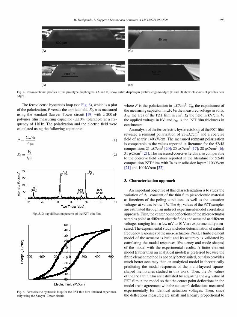
rode at a positive potential. Fig. 9 shows a plot of the appliedoltages versus center deflections of various microactuator sam-
les poled at different electric fields (voltages). The plot showshat the deflection versus actuation voltage behavior is nearlyinear within the low voltage range (0–800 mV) and the deflec-ions increase with increasing poling field.icroactuator obtained using the MSV.
M. Deshpande, L. Saggere / Sensors and
Fpa
vt2i(t
itam
5
waetptSbmrtl
Fi
ig. 9. Plots of center point deflections of the PZT thin film microactuatorsoled at various electric fields (values shown in the legend) as a function of thepplied actuation voltage in the range 100–800 mV.
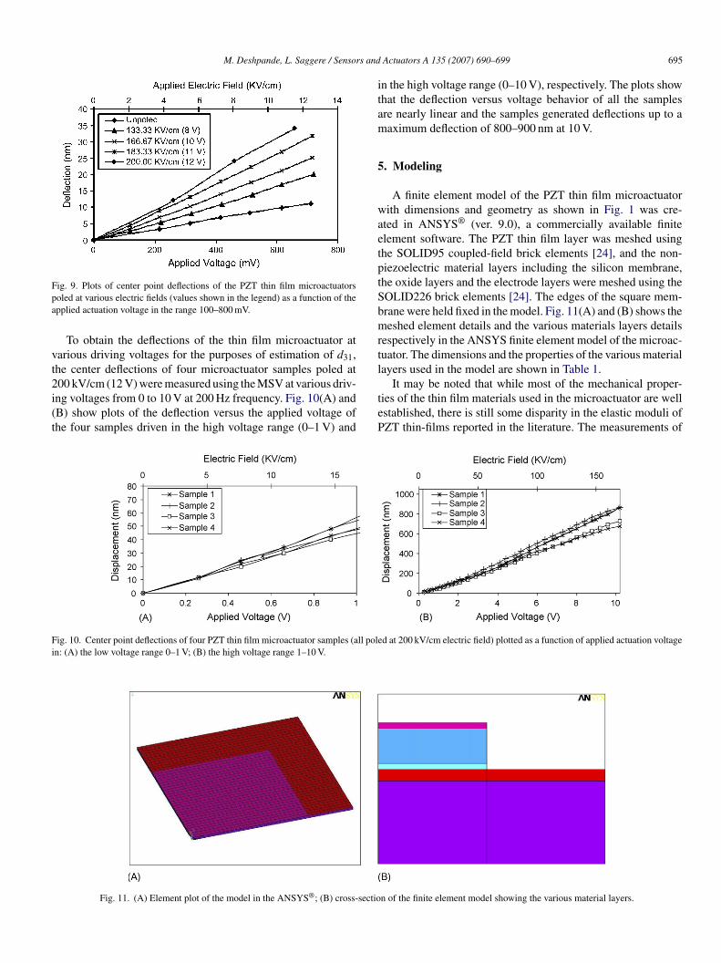
To obtain the deflections of the thin film microactuator atarious driving voltages for the purposes of estimation of d31,he center deflections of four microactuator samples poled at
00 kV/cm (12 V) were measured using the MSV at various driv-ng voltages from 0 to 10 V at 200 Hz frequency. Fig. 10(A) andB) show plots of the deflection versus the applied voltage ofhe four samples driven in the high voltage range (0–1 V) andteP
ig. 10. Center point deflections of four PZT thin film microactuator samples (all polen: (A) the low voltage range 0–1 V; (B) the high voltage range 1–10 V.
Fig. 11. (A) Element plot of the model in the ANSYS®; (B) cross-sectio
Actuators A 135 (2007) 690–699 695
n the high voltage range (0–10 V), respectively. The plots showhat the deflection versus voltage behavior of all the samplesre nearly linear and the samples generated deflections up to aaximum deflection of 800–900 nm at 10 V.
. Modeling
A finite element model of the PZT thin film microactuatorith dimensions and geometry as shown in Fig. 1 was cre-
ted in ANSYS® (ver. 9.0), a commercially available finitelement software. The PZT thin film layer was meshed usinghe SOLID95 coupled-field brick elements [24], and the non-iezoelectric material layers including the silicon membrane,he oxide layers and the electrode layers were meshed using theOLID226 brick elements [24]. The edges of the square mem-rane were held fixed in the model. Fig. 11(A) and (B) shows theeshed element details and the various materials layers details
espectively in the ANSYS finite element model of the microac-uator. The dimensions and the properties of the various materialayers used in the model are shown in Table 1.
It may be noted that while most of the mechanical proper-ies of the thin film materials used in the microactuator are wellstablished, there is still some disparity in the elastic moduli ofZT thin-films reported in the literature. The measurements of
d at 200 kV/cm electric field) plotted as a function of applied actuation voltage
n of the finite element model showing the various material layers.

696 M. Deshpande, L. Saggere / Sensors and Actuators A 135 (2007) 690–699
Table 1Dimension and property of materials of the microactuator used in the finite element model
Layers (↓) Structural dimensions Material properties
Thickness (�m) Length × width (�m2) Elastic modulus (GPa) Poisson’s ratio Density (kg/m3)
Silicon 13 1600 × 1600 168.9 [28,29] 0.182 [29] 2330Oxide 0.2 1600 × 1600 70 0.3 2200PPS
tpdt
Fa
latinum 0.1 1160 × 1160ZT 0.6 1160 × 1160ilver 0.1 1160 × 1160
he elastic properties of PZT thin film materials are more com-licated than their bulk counterparts due to their extremely smallimensions along thickness direction as well as the influence ofhe substrate on which they are fabricated [10]. Published values
fTtl
ig. 12. Natural mode shapes of the microactuator: (A), (B) and (C) are modes at 65nd (D), (E) and (F) are modes at 64.7, 133.7 and 197.9 kHz, respectively, obtained t
170 [30] 0.38 21450101 [14,15,20] 0.3 750082.7 [30] 0.37 10490
or PZT thin film elastic moduli have ranged from 37 to 400 GPa.his discrepancy in the PZT elastic moduli is generally believed
o be a source of the disparities among d31 values reported in theiterature because calculation of d31 requires the knowledge of
.2, 133.5 and 195.5 kHz, respectively, experimentally obtained using the MSV,hrough a finite element analysis.

M. Deshpande, L. Saggere / Sensors and Actuators A 135 (2007) 690–699 697
Table 2Experimentally measured and computed resonance frequencies of themicroactuator
Modes (↓) Measured frequenciesusing the MSV (kHz)
Computed frequencies in finiteelement analysis (kHz)
I 65.23 64.75II 133.48 133.71III 195.54 197.88IV 244.84 242.32V 249.10 243.84VI 301.41 304.24VV
tcuuthv
mmfcEtmf(cioa
etpfimap
6
reib
vefidt
Fm
sfitd
ut0dfrtrtataof −55 pC/N. The behavior of increase in d31 coefficient of apiezoelectric material with the increase in the actuation fieldof the PZT thin film samples is consistent with observations inother studies where a dc bias has been reported to improve the
II 400.43 407.69IIII 451.84 452.61
he PZT elastic modulus [15]. However, for thin films of 52/48ompositions PZT, elastic modulus value of 101 GPa is widelysed in many studies [14,15,20]. Recent experimental studiessing the nano-indentation technique [25,26] and wafer deflec-ion method [27] have found the modulus value to be in theigher end of the range 90–120 GPa. Based on these reports, aalue of 101 GPa is used in the current finite element model.
In order to validate the finite element model along with theaterial properties assumed, a modal analysis of the finite ele-ent model of the actuator was carried out and the analytical
requency data was compared with the corresponding frequen-ies that were obtained experimentally (see Table 2 and Fig. 12).ight frequencies and corresponding modes were extracted from
he model using the block-Lanczos method using a full plateodel of the actuator [24]. The experimentally obtained natural
requencies (Table 2, column 1) and the first three mode shapesFig. 12(A)–(C)) and the analytically obtained natural frequen-ies (Table 2, column 2) and mode shapes (Fig. 12(D)–(F)) aren very good agreement. This agreement validates the accuracyf finite element model as well as the material property valuesssumed in the finite element analysis.
The validated finite element model of the actuator is used toxtract the d31 coefficient of the PZT thin films. For this purpose,he voltage-induced deflections of the microactuator were com-uted using a quarter-symmetric model of the above validatednite element model. The bottom side of the PZT layer wasaintained at a zero potential, while varying negative voltages
re applied on the top side. An illustrative deflection contourlot of the microactuator is shown in Fig. 13.
. Discussion of the results
Using the approach described in Section 3 (Eq. (3)) and theesults of the experiments and the finite element analysis, thestimations of d31 values of the PZT thin film for various pol-ng conditions and for various actuation voltages are discussedelow.
To study the effect of PZT poling electric fields on the d31alues of the samples, d31 values at each measured deflection of
ach of the four microactuator samples poled at different electricelds in Fig. 9 were estimated. The average of the computed31 values corresponding to the microactuator deflections overhe low voltage actuation range for each microactuator polingFfo
ig. 13. A displacement contour plot from a finite element analysis of theicroactuator for an actuation voltage of 1 V applied across the PZT layer.
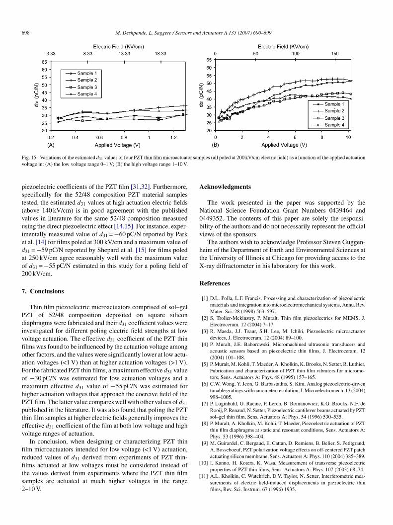
ample is plotted in Fig. 14 as a function of the poling electriceld. The d31 value for this actuation voltage range is found
o increase with the poling field, reaching a maximum value of31 = −30 pC/N.
To study the effect of actuation voltage on the d31 val-es of the samples, d31 values at each measured deflection ofhe four samples poled at 200 kV/cm and actuated at voltages–10 V in Fig. 10(A) and (B) were estimated using the approachiscussed above. These estimated d31 values are plotted as aunction of the applied actuation voltage for both low voltageange and high voltage range in Fig. 15. As seen in Fig. 15,he d31 values generally increase with the applied voltage andeach a limiting value as the actuating electric field approacheshe PZT coercive field of 140 kV/cm. For low actuation volt-ges up to 1 V (16.7 kV/cm), the d31 value is found to be inhe range of −25 to −30 pC/N, and for higher actuation volt-ges near 10 V (170 kV/cm), the d31 reaches a maximum value
ig. 14. Variation of the estimated average d31 value of the PZT thin film as aunction of the poling electric field for samples actuated in the low voltage rangef 0–800 mV.
698 M. Deshpande, L. Saggere / Sensors and Actuators A 135 (2007) 690–699
F r samv
pst(vuiedao2
7
PdivfioaFomhPptev
firfits2
A
N0bv
htX
R
ig. 15. Variations of the estimated d31 values of four PZT thin film microactuatooltage in: (A) the low voltage range 0–1 V; (B) the high voltage range 1–10 V.
iezoelectric coefficients of the PZT film [31,32]. Furthermore,pecifically for the 52/48 composition PZT material samplesested, the estimated d31 values at high actuation electric fieldsabove 140 kV/cm) is in good agreement with the publishedalues in literature for the same 52/48 composition measuredsing the direct piezoelectric effect [14,15]. For instance, exper-mentally measured value of d31 = −60 pC/N reported by Parkt al. [14] for films poled at 300 kV/cm and a maximum value of31 = −59 pC/N reported by Shepard et al. [15] for films poledt 250 kV/cm agree reasonably well with the maximum valuef d31 = −55 pC/N estimated in this study for a poling field of00 kV/cm.
. Conclusions
Thin film piezoelectric microactuators comprised of sol–gelZT of 52/48 composition deposited on square siliconiaphragms were fabricated and their d31 coefficient values werenvestigated for different poling electric field strengths at lowoltage actuation. The effective d31 coefficient of the PZT thinlms was found to be influenced by the actuation voltage amongther factors, and the values were significantly lower at low actu-tion voltages (<1 V) than at higher actuation voltages (>1 V).or the fabricated PZT thin films, a maximum effective d31 valuef −30 pC/N was estimated for low actuation voltages and aaximum effective d31 value of −55 pC/N was estimated for
igher actuation voltages that approach the coercive field of theZT film. The latter value compares well with other values of d31ublished in the literature. It was also found that poling the PZThin film samples at higher electric fields generally improves theffective d31 coefficient of the film at both low voltage and higholtage ranges of actuation.
In conclusion, when designing or characterizing PZT thinlm microactuators intended for low voltage (<1 V) actuation,educed values of d derived from experiments of PZT thin-
31lms actuated at low voltages must be considered instead ofhe values derived from experiments where the PZT thin filmamples are actuated at much higher voltages in the range–10 V.
[
[
ples (all poled at 200 kV/cm electric field) as a function of the applied actuation
cknowledgments
The work presented in the paper was supported by theational Science Foundation Grant Numbers 0439464 and449352. The contents of this paper are solely the responsi-ility of the authors and do not necessarily represent the officialiews of the sponsors.
The authors wish to acknowledge Professor Steven Guggen-eim of the Department of Earth and Environmental Sciences athe University of Illinois at Chicago for providing access to the-ray diffractometer in his laboratory for this work.
eferences
[1] D.L. Polla, L.F. Francis, Processing and characterization of piezoelectricmaterials and integration into microelectromechanical systems, Annu. Rev.Mater. Sci. 28 (1998) 563–597.
[2] S. Trolier-Mckinstry, P. Muralt, Thin film piezoelectrics for MEMS, J.Electroceram. 12 (2004) 7–17.
[3] R. Maeda, J.J. Tsaur, S.H. Lee, M. Ichiki, Piezoelectric microactuatordevices, J. Electroceram. 12 (2004) 89–100.
[4] P. Muralt, J.E. Baborowski, Micromachined ultrasonic transducers andacoustic sensors based on piezoelectric thin films, J. Electroceram. 12(2004) 101–108.
[5] P. Muralt, M. Kohli, T. Maeder, A. Kholkin, K. Brooks, N. Setter, R. Luthier,Fabrication and characterization of PZT thin film vibrators for micromo-tors, Sens. Actuators A: Phys. 48 (1995) 157–165.
[6] C.W. Wong, Y. Jeon, G. Barbastathis, S. Kim, Analog piezoelectric-driventunable gratings with nanometer resolution, J. Microelectromech. 13 (2004)998–1005.
[7] P. Luginbuhl, G. Racine, P. Lerch, B. Romanowicz, K.G. Brooks, N.F. deRooij, P. Renaud, N. Setter, Piezoelectric cantilever beams actuated by PZTsol–gel thin film, Sens. Actuators A: Phys. 54 (1996) 530–535.
[8] P. Muralt, A. Kholkin, M. Kohli, T. Maeder, Piezoelectric actuation of PZTthin film diaphragms at static and resonant conditions, Sens. Actuators A:Phys. 53 (1996) 398–404.
[9] M. Guirardel, C. Bergaud, E. Cattan, D. Remiens, B. Belier, S. Petitgrand,A. Bosseboeuf, PZT polarization voltage effects on off-centered PZT patchactuating silicon membrane, Sens. Actuators A: Phys. 110 (2004) 385–389.
10] I. Kanno, H. Kotera, K. Wasa, Measurement of transverse piezoelectricproperties of PZT thin films, Sens. Actuators A: Phys. 107 (2003) 68–74.
11] A.L. Kholkin, C. Wutchrich, D.V. Taylor, N. Setter, Interferometric mea-surements of electric field-induced displacements in piezoelectric thinfilms, Rev. Sci. Instrum. 67 (1996) 1935.

s and
[
[
[
[
[
[
[
[
[
[
[
[
[
[
[
[
[
[
[
[
[
B
MaHCaadi
LOfnMIeMA from 1999 to 2001. Since 2001, he has been at the University of Illinoisat Chicago, where he is currently an assistant professor of mechanical engi-
M. Deshpande, L. Saggere / Sensor
12] M. Deshpande, L. Saggere, Modeling and design of an optically pow-ered microactuator for a microfluidic dispenser, J. Mech. Des. 127 (2005)825–836.
13] M. Deshpande, L. Saggere, Development of a light-driven thin film piezo-electric microactuator, in: Proceedings of the 2005 ASME InternationalMechanical Engineering Congress and Symposium, Orlando, FL, Novem-ber 8–11, 2005.
14] G. Park, J. Choi, J. Ryu, H. Fan, H. Kim, Measurement of piezoelectriccoefficients of lead zirconate titanate thin films by strain-monitoring pneu-matic loading method, Appl. Phys. Lett. 80 (2002) 4606–4608.
15] J.F. Shepard Jr., P.J. Moses, S. Trolier-McKinstry, Wafer flexure techniquefor the determination of the transverse piezoelectric coefficient (d31) ofPZT thin films, Sens. Actuators A: Phys. 71 (1998) 133–138.
16] Y. Jeon, C.W. Wong, S. Kim, Water-immersible micromachined Pb(Zr,Ti)O3 thin film actuators, J. Electroceram. 13 (2004) 509–513.
17] K. Yamashita, H. Katata, M. Okuyama, H. Miyoshi, G. Kato, S. Aoyagi,Y. Suzuki, Arrayed ultrasonic microsensors with high directivity for in-airuse using PZT thin film on silicon diaphragms, Sens. Actuators A: Phys.97/98 (2002) 302–307.
18] L. Lian, N.R. Sottos, Effects of thickness on the piezoelectric and dielectricproperties of lead zirconate titanate thin films, J. Appl. Phys. 87 (2000)3941–3949.
19] C.B. Sawyer, C.H. Tower, Rochelle salt as a dielectric, Phys. Rev. 35 (1930)269–273.
20] R.A. Wolf, S. Trolier-McKinstry, Temperature dependence of the piezo-electric response in lead zirconate titanate films, J. Appl. Phys. 95 (2004)1397–1406.
21] S. Watanabe, T. Fujiu, T. Fujii, Effect of poling on piezoelectric propertiesof lead-zirconate-titanate thin-films formed by sputtering, Appl. Phys. Lett.66 (1995) 1481–1483.
22] S. Watanabe, T. Fujii, Micro-fabricated piezoelectric cantilever for atomicforce microscopy, Rev. Sci. Instrum. 67 (1996) 3898.
23] A.L. Kholkin, D.V. Taylor, N. Setter, Poling effect on the piezoelectricproperties of lead zirconate titanate thin films, in: Proceedings of the IEEEInternational Symposium on Applied, Ferroelectrics, August 24–27, 1998,pp. 69–72.
24] ANSYS Inc., Element Reference Guide, ANSYS Release 9.0 Documenta-tion, ANSYS Inc.
25] T. Fang, S. Jian, D. Chuu, Nanomechanical properties of lead zirconate
titanate thin films by nanoindentation, J. Phys.: Condens. Mat. 15 (2003)5253–5259.26] P. Delobelle, O. Guillon, E. Fribourg-Blanc, C. Soyer, E. Cattan, D.Remiens, True Young modulus of Pb(Zr,Ti)O3 films measured by nanoin-dentation, Appl. Phys. Lett. 85 (2004) 5185–5187.
naC
Actuators A 135 (2007) 690–699 699
27] J. Zhou, T. McMcollough, S.C. Mantell, S. Zurn, Young’s modulus mea-surement of thin film PZT, in: Microelectr. Symp. Proc., Jun 20–23, 1999,pp. 153–157.
28] T. Yi, L. Li, C. Kim, Microscale material testing of single crystalline silicon:process effects on surface morphology and tensile strength, Sens. ActuatorsA: Phys. 83 (2000) 172–178.
29] W.A. Brantley, Calculated elastic constants for stress problems asso-ciated with semiconductor devices, J. Appl. Phys. 44 (1973) 534–535.
30] S.P. Murarka, Metallization: Theory and practice for VLSI and ULSI,Butterworth-Heinemann, Boston, 1993.
31] N. Ledermann, P. Muralt, J. Baborowski, S. Gentil, K. Mukati, M. Cantoni,A. Seifert, N. Setter, {1 0 0}-textured, piezoelectric Pb(Zrx, Ti1−x)O3 thinfilms for MEMS: integration, deposition and properties, Sens. ActuatorsA: Phys. 105 (2003) 162–170.
32] J. Cho, M. Anderson, R. Richards, D. Bahr, C. Richards, Optimization ofelectromechanical coupling for a thin film PZT membrane. II. Experiment,J. Micromech. Microeng. (2005) 1804–1809.
iographies
andar Deshpande is currently a PhD candidate in mechanical engineeringt University of Illinois at Chicago and is expected to graduate in Fall 2006.e received a BS degree in mechanical engineering from Regional Engineeringollege, Surat, India, in 2001. His research interests include design, modelingnd fabrication of MEMS devices particularly integrating technologies, suchs piezoelectric thin films and photovoltaics, to create novel cross-functionalevices. He is a student member of ASME and a recipient of Sigma-Xi Grant-n-Aid of research award for vision research in 2004.
axman Saggere received his BE degree in mechanical engineering from thesmania University, India, in 1987, an MS degree in mechanical engineering
rom the University of Rhode Island in 1993, an MS degree in aerospace engi-eering and a PhD degree in mechanical engineering from the University ofichigan at Ann Arbor, MI, in 1998. He served as a scientist-engineer in the
ndian Space Research Organization from 1987 to 1991, and as a research sci-ntist in the Department of Aeronautics and Astronautics at MIT, Cambridge,
eering. His primary research interest is in the design, development and novelpplications of MEMS and bioMEMS technologies. He is a recipient of the NSFAREER award.
Copyright © 2022 FDOKUMEN