PROJECT DOCUMENTATION - Sacramento State
117
C ALIFORNIA S TATE U NIVERSITY S ACRAMENTO CHILD SAFETY: P ROJECT DOCUMENTATION P ROJECT GUARDIAN Authors: Zohaib ARSHAD Jashanjit BADWAL Leonardo JACOBO Didier MPONTE Harpreet S IDHU Instructor: Dr. BELKHOUCHE November 30, 2015
-
Upload
khangminh22 -
Category
Documents
-
view
2 -
download
0
Transcript of PROJECT DOCUMENTATION - Sacramento State

CALIFORNIA STATE UNIVERSITY SACRAMENTO
CHILD SAFETY: PROJECT DOCUMENTATION
PROJECT GUARDIAN
Authors:Zohaib ARSHAD
Jashanjit BADWALLeonardo JACOBODidier MPONTEHarpreet SIDHU
Instructor:Dr. BELKHOUCHE
November 30, 2015
i
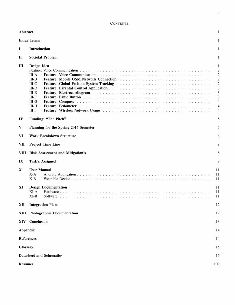
CONTENTS
Abstract 1
Index Terms 1
I Introduction 1
II Societal Problem 1
III Design Idea 1Feature: Voice Communication . . . . . . . . . . . . . . . . . . . . . . . . . . . . . . . . . . . . . . . . . . . . . . 2III-A Feature: Voice Communication . . . . . . . . . . . . . . . . . . . . . . . . . . . . . . . . . . . . . . . . 2III-B Feature: Mobile GSM Network Connection . . . . . . . . . . . . . . . . . . . . . . . . . . . . . . . . 2III-C Feature: Global Position System Tracking . . . . . . . . . . . . . . . . . . . . . . . . . . . . . . . . . 2III-D Feature: Parental Control Application . . . . . . . . . . . . . . . . . . . . . . . . . . . . . . . . . . . . 3III-E Feature: Electrocardiogram . . . . . . . . . . . . . . . . . . . . . . . . . . . . . . . . . . . . . . . . . . 3III-F Feature: Panic Button . . . . . . . . . . . . . . . . . . . . . . . . . . . . . . . . . . . . . . . . . . . . . 3III-G Feature: Compass . . . . . . . . . . . . . . . . . . . . . . . . . . . . . . . . . . . . . . . . . . . . . . . 4III-H Feature: Pedometer . . . . . . . . . . . . . . . . . . . . . . . . . . . . . . . . . . . . . . . . . . . . . . 4III-I Feature: Wireless Network Usage . . . . . . . . . . . . . . . . . . . . . . . . . . . . . . . . . . . . . . 4
IV Funding: “The Pitch” 5
V Planning for the Spring 2016 Semester 5
VI Work Breakdown Structure 6
VII Project Time Line 8
VIII Risk Assessment and Mitigation’s 8
IX Task’s Assigned 8
X User Manual 11X-A Android Application . . . . . . . . . . . . . . . . . . . . . . . . . . . . . . . . . . . . . . . . . . . . . . . 11X-B Wearable Device . . . . . . . . . . . . . . . . . . . . . . . . . . . . . . . . . . . . . . . . . . . . . . . . . 11
XI Design Documentation 11XI-A Hardware . . . . . . . . . . . . . . . . . . . . . . . . . . . . . . . . . . . . . . . . . . . . . . . . . . . . . 11XI-B Software . . . . . . . . . . . . . . . . . . . . . . . . . . . . . . . . . . . . . . . . . . . . . . . . . . . . . 11
XII Integration Plans 12
XIII Photographic Documentation 12
XIV Conclusion 13
Appendix 14
References 14
Glossary 15
Datasheet and Schematics 16
Resumes 109

ii
LIST OF FIGURES
1 Work Breakdown Structure Diagram . . . . . . . . . . . . . . . . . . . . . . . . . . . . . . . . . . . . . . . . . . . 72 Application Overview . . . . . . . . . . . . . . . . . . . . . . . . . . . . . . . . . . . . . . . . . . . . . . . . . . . 113 Application Communication . . . . . . . . . . . . . . . . . . . . . . . . . . . . . . . . . . . . . . . . . . . . . . . 114 Application Miscellaneous . . . . . . . . . . . . . . . . . . . . . . . . . . . . . . . . . . . . . . . . . . . . . . . . 115 GSM/GPRS/GPS . . . . . . . . . . . . . . . . . . . . . . . . . . . . . . . . . . . . . . . . . . . . . . . . . . . . . 126 Intel Edison Chip . . . . . . . . . . . . . . . . . . . . . . . . . . . . . . . . . . . . . . . . . . . . . . . . . . . . . 127 Intel Edison Board . . . . . . . . . . . . . . . . . . . . . . . . . . . . . . . . . . . . . . . . . . . . . . . . . . . . 128 GSM/GPRS/GPS Working Prototype . . . . . . . . . . . . . . . . . . . . . . . . . . . . . . . . . . . . . . . . . . . 13
LIST OF TABLES
I Work Breakdown Structure . . . . . . . . . . . . . . . . . . . . . . . . . . . . . . . . . . . . . . . . . . . . . . . . 6II Project Time Line . . . . . . . . . . . . . . . . . . . . . . . . . . . . . . . . . . . . . . . . . . . . . . . . . . . . . 8III Zohaib’s Assignments . . . . . . . . . . . . . . . . . . . . . . . . . . . . . . . . . . . . . . . . . . . . . . . . . . . 9IV Jashanjit’s Assignments . . . . . . . . . . . . . . . . . . . . . . . . . . . . . . . . . . . . . . . . . . . . . . . . . . 9V Leonardo’s Assignments . . . . . . . . . . . . . . . . . . . . . . . . . . . . . . . . . . . . . . . . . . . . . . . . . 9VI Didier’s Assignments . . . . . . . . . . . . . . . . . . . . . . . . . . . . . . . . . . . . . . . . . . . . . . . . . . . 9VII Harpreet’s Assignments . . . . . . . . . . . . . . . . . . . . . . . . . . . . . . . . . . . . . . . . . . . . . . . . . . 10VIII Hours Per Assignment . . . . . . . . . . . . . . . . . . . . . . . . . . . . . . . . . . . . . . . . . . . . . . . . . . 10

1
CHILD SAFETY: Project DocumentationZohaib Arshad∗, Jashanjit Badwal†, Leonardo Jacobo‡ and Didier Mponte§, and Harpreet Sidhu¶
Department of Computer and Electrical Engineering, California State University SacramentoSacramento, CA USA
Email: ∗[email protected], †[email protected], ‡[email protected], §[email protected], ¶[email protected]
Abstract—One of the hardest, and sometimes scariest, things fora parent to do is let their child walk out that door alone to be gonefor the next eight to sixteen hours. Sure theyre more than likely atschool or out with close family friends but there are those timesin between, en route, where anything can happen. A child canget lost, run away, or worse yet get kidnapped! These are someof things parents take into consideration when allowing or notallowing their child to go out on their own. Parents and guardianswant assurance that their child is safe at their destination andwill return home safe and sound. Team Child Safety wants to givethese parents peace of mind while their children are not withintheir grasp. We are doing this by creating a mobile applicationfor the parent to interface with their child who will wear ourwearable device that will provide the childs location, captureheart rate data, and allow the child and parent/guardian tocommunicate via text messaging and voice communication. It willbe as if the child is always within reach. This paper will go intomore detail as to how our device will operate along with providethe reader with some statistics regarding child safety gatheredthrough research.
Keywords—Wearable, child, safety, kidnapping, missing, apps,mobile, gps, iot.
I. INTRODUCTION
The Laboratory prototype documentation will cover thefollowing portions: Problem statement, Design idea with punchlist, work breakdown structure and time line (year-long por-tions), as well as photographic documentation from work com-pleted. Along with an additional portion going over the teamsparticipation in the competition, The Pitch, no other team in thesenior design class was part of. The report contains executivesummaries that contains a synopsis of all the sections, writtenspecifically by the members that have completed work in thatspecific area. The document will also contain a user guideto help the user understand both the application and device.Along with the proper documentation, the report will alsoaccommodate preliminary testing results.
II. SOCIETAL PROBLEM
Research conducted by Team Child Safety during the Fallsemester of 2015 displayed that there is a societal need for adevice to help reduce the amount of children that are reportedmissing each year and to help track children that become lost orkidnapped. From the research, the team conducted, it becameevident, that this truly was a very serious problem in today’ssociety. In the United States alone, there were at least 466,949children reported missing by the National Crime InformationCenter (NCIC). In 2013, this number was at least 462,567. [1]
As the statics show, the number of children reported missingis steadily increasing.
Many predators use social media sites such as Facebook tocontact underage children and trick them into meeting them.Youtuber, Coby Persin, set out to perform a social experimentwhich revealed how easy it can be for someone to kidnap achild using Facebook. [2] YouTuber Coby Persin carried out achild predator test with the agreement of the families of threechildren one who was 14, another who was 13 and a thirdwho was just 12. Mikayla, 13, started chatting with Coby viaa fake Facebook profile for a 15-year-old boy called JasonBiazzo. Just four days later she not only gave him her mobilephone number but she agreed to meet him in her local park.Butafter arriving she is shocked to find her father there waiting forher instead and he is not happy at all.”You realise how scarythis could have been?”, he tells her. [2] Next up is a 12-year-old girl called Julianna, who agrees with ”Jason” that he cancome to her house after her father had fallen asleep. Julianna,who also offered up her telephone number without a secondthought, texted him saying: ”LOL. I would have to wait untilmy dad falls asleep if you want to chill cos I cant have boysover.” Again, Julianna invited him inside and her father (whowas not asleep) was not happy at all.”Whats wrong with you?”he said. You could have been raped or murdered. I love you.Dont you ever do this again. The third youngster was calledJenna a 14-year-old who again handed over her phone number.This time the parents allowed Cory to pretend to kidnap herin a van to demonstrate the dangers of chatting to strangersonline. [2]
All three of these innocent girls did not understand howdangerous the world can be and learned valuable lessonsthat day. The outcome may have been much worse. Thisis something that occurs every day. Predators finding newmethods to contact underage children and tricking them intomeeting them.
III. DESIGN IDEA
With the information Team Child Safety has gathered fromresearching, a consensus was reach on how the team shouldapproach the societal issue. Team Child Safety wants to createa device which will provide location data to enhance the searchefforts of missing minors. By allowing parents to track theposition of their children through a app on a smart phone, theparents are given more comfort of where their children trulyare. Team Child Safety will cover S.W.A.T (Smart WearableAdolescence Tracker) in more detail throughout this report.
The design has three major focal points. The wearabledevice, a smart phone application and a central data processing
2
center. The goal is to keep this wearable as light, user friendlyand comfortable as possible while sending vital informationto the paired smart phone. The smart phone app will receiveinformation from the wearable such as location. The centraldata processing center will be used to process the informationfrom the watch to the app.
The design helps to solve the societal problem, by givingchildren who are in need, a device that can be used to contactfor help. Children will be able contact for help, at will, whenthey are in a frightening situation. Parents will also be ableto track their children through the mobile phone application.Giving the users a sense of security and comfort. With sucha device implemented, Team Child Safety will give childrenthat are in need of help, a way to inform their guardian.For example if a child is kidnapped, being followed or lost,the device will have GPS, voice communication and a panicbutton, all of which can be used to contact for help or befound.
A. Feature: Voice Communication
Voice communication is a key aspect for a parent or guardianto have with their child. This feature allows the user, namelythe child. the parent or guardian, to communicate with oneanother verbally. The reasoning behind this, is to keep the childin a calm state of mind. Talking with ones parent or guardian,in a time where one is panicking, can tremendously help. Aaddition to this feature is to allow communication with morethan one parental figure or guardian. Only a select number areallowed to communicate with the child.
For this feature to be enabled on the device, some hardwareis required. Team Child Safety has chosen an add-on modulefor the Intel Edison Platform. This module is the same onethat was chosen for Global Positioning System Tracking andGSM Mobile communication.
”The Diymall SIM808 GPS GSM GPRS Module for Ar-duino” was chosen as the add on module. [3]. In addition tothis add on module, Team Child Safety will be required tointegrate an antenna for the signal to transmit and receive dataon.
The software behind this feature will include the use of somepredefined libraries along with custom hand coded functionsand classes. [4] The coding for this feature will be done inC/C++ programming language since Arduino supports onlythese two langauges. The code will include a basic function-ality for calling and texting such as make and receive phonecalls, send and receive text messages, call disconnect, etc. Tocode for this platform. Team Child Safety have chosen to usea mixture of IDE’s from Jet Brains, namely the IntelliJ IDEA.[5]
It is absolutely crucial for this feature to work 100% of thetime. If this feature does not work properly many issues mayarise, as this is a feature can be used in a very emotional periodof time. One of the instances that this feature could not workproperly or could eventually fail is when the wearable deviceis in the basement of the building or it is in the area wherethere is poor reception.
To validate voice communication, testing must be done onthe data being sent in and out. All vocal transmissions must betested manually by two parties to confirm, what is being saidon the transmission is actually being received on the receiver.
The tests that will be conducted, include, but are not solelylimited to the following.
Also, the constant communication of the wearable devicewith the android application which will show the location ofthe child through GPS.
To determine if Voice communication is complete, all testslisted above need to completed. Along with the tests, fieldtesting needs to be done.
B. Feature: Mobile GSM Network Connection
The back end of communication with the mechanism anda data communicating server is all achieved with a MobileGSM Network, GSM, or Global System for Mobile Commu-nications. The Mobile GSM Network, is a definitive devel-oped by the European Telecommunications Standards Institute(ETSI) to construe protocols for second-generation (2G) digitalcellular networks used by mobile phones, first deployed inFinland in July 1991. [6] For Team Child safety, this resultsin being a key feature for the device to work properly. Thisfeature allows the device to transmit data wireless to the centraldata processing center. Basically, this is the gateway betweentransmitting and receiving data between a parent/guardian andhis or her child. This feature is crucial for the entire unit towork properly. If no data is being transmitted for received,then there is no tracking.
To validate Mobile GSM Network Connection, testing mustbe done on the data being sent in and out. All data that is sentin and out of the device must be validated. A CRC Check mustbe performed to determine the integrity of the data at hand.
C. Feature: Global Position System Tracking
Global Position System Tracking is another key feature for aparent to have with their child. This feature allows the user,namely the parent, to track their child. The reasoning behindthis, is to allow the parent to know about his or her child’swhereabouts. This can come in crucial if the child is lost oreven, in a worst case scenario, the child is kidnapped. This cantremendously help the proper authorities locate and retrieve achild, or even the parent if the child is lost.
For this feature to be enabled on the device, some hardwareis required. Team Child Safety has chosen an add on modulefor the Intel Edison Platform. This module is the same onethat was chosen for Voice Communication and GSM Mobilecommunication. ”The Diymall SIM808 GPS GSM GPRSModule for Arduino” was chosen as the add on module. [3].In addition to this add on module, Team Child Safety will berequired to integrate an antenna for the signal to transmit andreceive data on.
The software behind this feature will include the use of somepredefined libraries along with custom hand coded functions

3
and classes. [4] To code for this platform. Team Child Safetyhave chosen to use a mixture of IDE’s from Jet Brains, namelythe IntelliJ IDEA. [5]
It is absolutely crucial for this feature to work 100% of thetime. If this feature does not work properly many issues mayarise, as this is a feature can be used in a very emotional periodof time. The tests that will be conducted, include, but are notsolely limited to the following.
To determine if Global Positioning System Tracking iscomplete, all tests listed above need to completed. Along withthe tests, field testing needs to be done.
This feature in general may take a few weeks to complete. Itis a key feature, that is required to allow the device to functioncorrectly.
D. Feature: Parental Control Application
A Parental Control Application is required for this device. Fora parent to be able to communicate and locate his or her child,some type of mechanism is required. This is were the ParentalControl Application comes in. This is the central hub for aparent to use any functionality that the device the child wearswill offer. This feature is crucial for the entire unit to workproperly. If there is no way for the parent to communicate orlocate his or her child then there is no clear purpose for thedevice, generally speaking. With out this application, majorfunctionality is disabled.
For this feature to be enabled, the parent must have anAndroid smart phone. This hardware is not provided by TeamChild Safety. Team Child safety will provide an applicationthat is downloadable to the smart phone.
The software behind this feature will be hand coded in itsentirety using Android Studio as the IDE. This IDE is basedupon the IntelliJ platform that Jet Brains offers. [7]
It is absolutely crucial for this feature to work 100% of thetime. If this feature does not work properly many issues mayarise, as this is a feature can be used in a very emotional periodof time. The tests that will be conducted, include, but are notsolely limited to the following:
To determine if Parental Control Application is complete,all tests listed above need to completed. Along with the tests,field testing needs to be done.
This feature in general will be an on going process. Esti-mation for it’s complete is not readily available. There are toomany variables in determining the length of time that will betaken. It is a key feature that allows the parent to view viableand usable data.
E. Feature: Electrocardiogram
There are particular vitals that need to be watched on achild. One of the imperative vitals is the child’s pulse whichwill result in the child’s heart rate. Contemporary heart ratemonitors usually comprise two elements: a transmitter and areceiver, though, later units have used conductive smart fabric
with built-in microprocessors that inspects the Electrocardio-gram signal to determine heart rate. [8] This results in theElectrocardiogram, EKG becoming an essential feature for thisdevice. With an EKG enabled on this device, a parent is able toview quite a few vitals on his or her child. Some vitals includethe child’s pulse and if the device is attached to the child. Whenthis data is transmitted, it is first sent to the central processingcenter to be processed. The data is then refined and permeatedon the central processing center and then the processed andfiltered data is transmitted to the parental control application.The data given isn’t just a number, but instead a level. Theheart rate is then displayed in a friendly user interface, or UI.This UI will either display the heart rate in three forms. One,if the heart rate is within an acceptable range. Two, if it isstarting to climb. Three, if the heart rate is in a dangerouslyhigh range. There is also an option available to display thedata as a numerical amount instead. This level indicates ifthe child’s pulse is within reasonable values. If it is not thenthe parental application alerts the parent of this change. If thedevice is found to not be connected on the child this is alsoa good indicator that the child’s location may not be 100%valid. This feature is essential in providing useful feedback andmetrics for the parent. Without this feature being implemented,the devices functionality can be limited.
For this feature to be enabled, device requires a seriesof components. A series Operational Amplifier, capacitors,resistors, along with some electrodes are required to completethis feature.
The software behind this feature will be entirely hand codedwith a number of functions and classes. [4] To code for thisplatform. Team Child Safety have chosen to use a mixture ofIDE’s from Jet Brains, namely the IntelliJ IDEA. [5]
It is important for this feature to work. If this feature doesnot work properly, many of the metrics being sent to theparental application will not be enabled. The tests that will beconducted, include, but are not solely limited to the following.
To determine if Electrocardiogram is complete, all testslisted above need to completed. Along with the tests, fieldtesting needs to be done.
This feature in general will take a few weeks to complete. Itis a key feature that allows the parent to receive viable metricsdata on his or her child’s vitals.
F. Feature: Panic Button
If the situation ever occurs, where a child is being kidnappedor in danger for instance, the child is able to press the panicbutton on his or her watch. Briefly speaking, a panic buttonis an electronic component designed to assist in alerting anindividual in emergency situations where a threat to personsor property exists. [9] Which is exactly what a child in a diresituation needs.
This feature is essential in providing useful feedback andmetrics for the parent. Without this feature being implemented,the devices functionality can be limited.
For this feature to be incorporated on this device, there are afew components required. A button and resistors are required
4
for this feature.The software behind this feature will be entirely hand coded
with a number of functions and classes. [4] To code for thisplatform. Team Child Safety has chosen to use a mixture ofIDE’s from Jet Brains, namely the IntelliJ IDEA. [5]
It is important for this feature to work. If this feature doesnot work properly, the child could press the panic button andthe parent may never get a notification for this.
To determine if the Panic Button is complete, all tests listedabove need to completed. Along with the tests, field testingneeds to be done.
This feature in general will take a few weeks to complete.It is a key feature that allows the parent to receives criticalinformation on his or her child.
G. Feature: Compass
When locating a child, GPS is not always readily availablefor use. Backup forms of locating are necessary to add as failsafes for the overall system.
This feature is useful in providing secondary localizationdata. Without this feature being implemented, the device willnot have a fail safe back up when GPS does not functionproperly or is not readily available for use.
For this feature to be incorporated on this device, thereare a few components required. A Triple-axis Accelerome-ter+Magnetometer (Compass) Board - LSM303 [10], is re-quired to complete this feature.
The software behind this feature will be entirely hand codedwith a number of functions and classes. [4] To code for thisplatform. Team Child Safety has chosen to use a mixture ofIDE’s from Jet Brains, namely the IntelliJ IDEA. [5]
It is important for this feature to work. If this feature doesnot work properly, then there is no fail safe system in place.
To determine if Compass is complete, all tests listed aboveneed to completed. Along with the tests, field testing needs tobe done.
This feature in general will take a few weeks to complete. Itis a key feature that allows the parent to receives a secondarysource of information on his or her child.
H. Feature: Pedometer
When locating a child, GPS is not always readily availablefor use. A portable electronic device, that counts each stepa person takes by detecting the motion of the person’s hipsand hands can provide crucial pieces of information that canbe used to determine the number of steps that the child inparallel with the direction they are moving with a compass.[11] Backup forms of locating are necessary to add as failsafes for the overall system.
This feature is useful in providing secondary localizationdata. Without this feature being implemented, the device willnot have a fail safe back up when GPS does not functionproperly or is not readily available for use.
For this feature to be incorporated on this device, thereare a few components required. A Triple-axis Accelerome-ter+Magnetometer (Compass) Board - LSM303 [10], is re-quired to complete this feature.
The software behind this feature will be entirely hand codedwith a number of functions and classes. [4] To code for thisplatform. Team Child Safety has chosen to use a mixture ofIDE’s from Jet Brains, namely the IntelliJ IDEA. [5]
It is important for this feature to work. If this feature doesnot work properly, then there is no fail safe system in place.
To determine if Pedometer is complete, all tests listed aboveneed to completed. Along with the tests, field testing needs tobe done.
This feature in general will take a few weeks to complete. Itis a key feature that allows the parent to receives a secondarysource of information on his or her child.
I. Feature: Wireless Network Usage
Taking in consideration, the situation where a child may belost or kidnapped, for instance, GPS and GSM are not alwaysavailable in certain locations. There is the backup fail safe of acompass/pedometer feature, but this can only go so far. Thereneeds to be another alternative, this is where wireless networkusage comes into play. Everywhere around us, there are agrowing number of wireless networks, such as Wifi. It wouldonly make sense for this device to connect to them, as well, asanother source of data connection. Along with being anothersource of data connection, wireless networks have identifiers,that identify which network they are. This piece of informationcan be used in locating a child. This information will be storedand then sent to the Central data processing center for furtherstorage and usage.
This feature is useful in providing additional localizationdata and an alternative source of data connection.
Without this feature being implemented, the device will bemore limited in certain scenarios.
For this feature to be incorporated on this device, there area few components required. The Intel Edison Platform, will beused, as it has built in wifi and bluetooth radios. [12]
The software behind this feature will use a mixture ofpredefined libraries along many hand coded functions andclasses. [4] To code for this platform. Team Child Safety havechosen to use a mixture of IDE’s from Jet Brains, namely theIntelliJ IDEA. [5]
It is important for this feature to work. If this feature doesnot work properly, then there is no fail safe system in place.
1) Data Reliability• Verification of wireless networks being present.• Verification of wireless networks names being
stored.To determine if Wireless Network Usage is complete, all
tests listed above need to completed. Along with the tests,field testing needs to be done.
This feature in general will take a few weeks to complete.It is a key feature that allows the parent to receives additional
5
information on his or her child along with the device beingable to connect to an alternative data connection.
Data Transmission
When transmitting data, Team Child Safety will begin withseries of common steps for each feature which includes cyclicredundancy check, states are coded into the system. An errordetection is done through this code. Also, the verification ofbit rate for data transfer between CPU and add on module.Team Child Safety will also perform waveform test benchverification that all bits are being transferred correctly basedon the clock cycle.
Testing
To determine if each feature set is complete, a series of testwill be conducted. Along with the tests, field testing needs tobe done.
IV. FUNDING: “THE PITCH”The pitch is a competition hosted by the Center of En-
trepreneurship at Sacramento State along with the Associationof Collegiate Entrepreneurs. This competition is designed tohelp participants turn their solution to a problem in to a busi-ness. This event was closed to Sacramento State students, thewinners from this even would be able to attend the Future Fourcompetition. Team Child Safety decided that this competitionwould be a good way to get reimbursed and also providefunding for Project Guardian. The prizes for winning werethe following: First Place $700, Second Place $500, and ThirdPlace $300. It was the first time presenting Project Guardianoutside of the classroom, and to the team it seemed like a greatsuccess. Unfortunately, Team Child Safety was unable to placein the qualifying round, it did not discourage the team at all.The team considered this a valuable learning experience, andwill continue to participate in any competitions, and strive forgreatness.
V. PLANNING FOR THE SPRING 2016 SEMESTER
As the first half of our senior design winds down weare able to look back and take note of our successes whilealso looking into the future to the additional features to beadded to make our system great. We have been able to getthe following systems working: GSM communication, GPSlocalization, Heart rate sensor data, user verification, datastreaming, and our mobile application along with our website.Taking a closer look into next semester, we plan to implementthe following features: Panic Button, Battery and chargingmechanism, design of band, clock, pedometer, improving ourmobile application, and a feature which detects and stores otherphones wireless ids. The previously stated additional featuresto be implemented during the spring semester are fairly self-explanatory except for the last feature which I will explain inmore detail. In the event that a child is kidnapped, althoughthere will be our GPS module, law enforcement and especially
the parent/guardian would benefit from knowing who they aredealing with. To assist in this manner we plan to implementa feature that detects and stores surrounding phone wi-fi IDsas well as the time and length of time in which the phoneswere within range of the users wearable device. We believe thiswill potentially identify the kidnapper and make retrieving thechild a success. Along with our new features, we still planon continuously improving our current features and focusingon the actual build of the wearable. We are currently utilizingArduinos but plan to implement all of our features on the IntelEdison to improve and enhance processing as well as decreasein the size of the band to make it more aesthetically pleasingto the user.
6
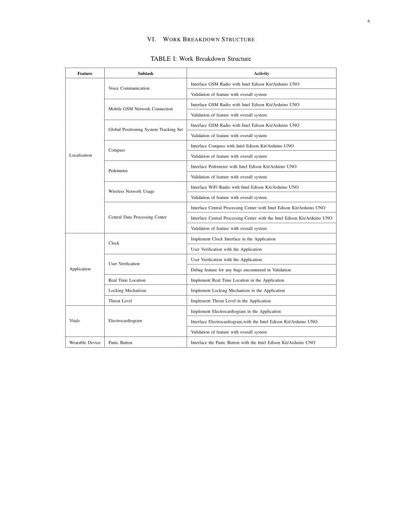
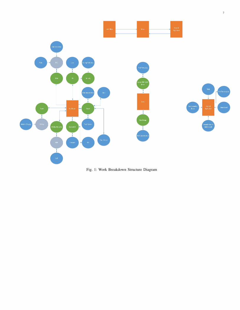
VI. WORK BREAKDOWN STRUCTURE
TABLE I: Work Breakdown Structure
Feature Subtask Activity
Localization
Voice CommunicationInterface GSM Radio with Intel Edison Kit/Arduino UNO
Validation of feature with overall system
Mobile GSM Network ConnectionInterface GSM Radio with Intel Edison Kit/Arduino UNO
Validation of feature with overall system
Global Positioning System Tracking SetInterface GSM Radio with Intel Edison Kit/Arduino UNO
Validation of feature with overall system
CompassInterface Compass with Intel Edison Kit/Arduino UNO
Validation of feature with overall system
PedometerInterface Pedometer with Intel Edison Kit/Arduino UNO
Validation of feature with overall system
Wireless Network UsageInterface WiFi Radio with Intel Edison Kit/Arduino UNO
Validation of feature with overall system
Central Data Processing Center
Interface Central Processing Center with Intel Edison Kit/Arduino UNO
Interface Central Processing Center with the Intel Edison Kit/Arduino UNO
Validation of feature with overall system
Application
ClockImplement Clock Interface in the Application
User Verification with the Application
User VerificationUser Verification with the Application
Debug feature for any bugs encountered in Validation
Real Time Location Implement Real Time Location in the Application
Locking Mechanism Implement Locking Mechanism in the Application
Threat Level Implement Threat Level in the Application
Vitals Electrocardiogram
Implement Electrocardiogram in the Application
Interface Electrocardiogram,with the Intel Edison Kit/Arduino UNO
Validation of feature with overall system
Wearable Device Panic Button Interface the Panic Button with the Intel Edison Kit/Arduino UNO
7
Fig. 1: Work Breakdown Structure Diagram

8
VII. PROJECT TIME LINE
TABLE II: Project Time Line
Tasks Due Date
Develop Working Prototype 12/04/15
Continue improving Working Prototype 04/25/16
Problem Statement Report 09/14/15
Design Idea Contract 09/28/15
Work Breakdown Structure 09/28/15
Project Timeline 10/12/14
Risk Assessment Report 12/26/15
End of Term Documentation 12/11/15
Revised Problem Statement 01/22/16
Device Test Plan Report 02/01/16
Market Review 02/29/16
Mid Term Review 3/14/16
Deploy-able Prototype Presentation 4/18/16
End of Project Presentation 5/19/16
Android Application 4/1/16
Voice Communication 11/27/15
Global Positioning Date 11/27/15
Server 11/27/15
Vitals 11/27/15
User Verification 11/27/15
Panic Button 1/11/16
Wireless Network Monitoring 1/11/16
Touch Screen Display 11/27/15
Compass/Pedometer 1/11/16
Battery 2/12/16
Wireless Charging 4/1/16
Integrating all components together 4/1/16
VIII. RISK ASSESSMENT AND MITIGATION’S
As Team Child Safety is working to develop a wearabledevice for children that will be synced to a mobile appin which their parents will be able to view the status oftheir safety, health, and whereabouts, there are many risksto take in consideration. The four main features that pose asthe four main risk, if execution fails, are localization, voicecommunication, the mobile application, and user verification.
Localization is critical in our design as it allows the par-ent/guardian the ability to view their child’s location as thechild wears the wearable which contains a GPRS and GSMmodule. The GPRS module is what enables the localizationbut cannot work properly unless paired with the GSM modulewhich provides it the ability to send the location data to themobile application for the parent/guardian to view. One ofthe goals of this product is to provide the parent/guardianwith the ability to view their child’s whereabouts and if ourGPRS/GSM module fails then the entire product fails. Wecurrently have this feature up and running and our goal fornext semester is to incorporate a fail safe feature in case thisfails which will incorporate an inertial measurement unit whichwill provide back up localization data. In conjunction with ourlocalization feature, we are providing the ability for the childto communicate with the parent/guardian directly via voicecommunication and text messaging. We currently do not haveany back up communication services if this feature were tocompletely fail but in the event that this feature were to fail,the parent/guardian will be notified via the mobile app and thewearable device.
The mobile application is one of the cornerstones of ourwearable device as it provides the parent/guardian with thenecessary data on their child. In the event that this featurefails to execute, our device will then begin to send the pertinentdata via text messaging directly to the parents device. One ofour biggest fears is our device ending up in the wrong handsand being manipulated by a thief, which could potentially alterand provide false data to the parent/guardian. To combat thiswe will be utilizing a user verification method which requiresthe user to input a password in order to register, utilize, andview data on the device. With our combined efforts we hopeto provide the user and parent/guardian with an extra pair ofeyes that is with their child even when their child is not withintheir sight.
IX. TASK’S ASSIGNED
Each member of the group was assigned certain features ofthis project depending on skill set, what they wanted to workon and the work load of each feature.
Below is a table with shows the tasks Zohaib Arshad workedon this semester.
9
TABLE III: Zohaib’s Assignments
Task Hours
Problem Statement Report 20 Hours
Design Idea Report 25 Hours
Work Breakdown Report 32 Hours
Project Time line 10 Hours
Risk Assessment Report 3 Hours
Heart Rate Sensor 12 Hours
Android Application 2 Hours
Localization Feature 10 Hours
Voice Communication Feature 29 Hours
Shield Debugging 7 Hours
Global Positioning System Feature 10 Hours
Setting up Intel Edison 5 Hours
Implement GPS/GSM Shield with Intel Edison 10 Hours
The Pitch Competition 8 Hours
Laboratory Prototype Documentation 10 Hours
Total 193 Hours
Below is a table with shows the tasks Jashanjit Badwalworked on this semester.
TABLE IV: Jashanjit’s Assignments
Task Hours
Problem Statement Report 20 Hours
Design Idea Report 25 Hours
Work Breakdown Report 32 Hours
Project Timeline 10 Hours
Risk Assessment Report 3 Hours
Heart Rate Sensor 4 Hours
Android Application 5 Hours
Localization Feature 8 Hours
Voice Communication 59 Hours
Laboratory Prototype Documentation 15 Hours
Total 181 Hours
Below is a table with shows the tasks Leonardo Jacoboworked on this semester.
TABLE V: Leonardo’s Assignments
Task Hours
Problem Statement Report 20 Hours
Design Idea Report 25 Hours
Work Breakdown Report 32 Hours
Project Time line 10 Hours
Risk Assessment Report 3 Hours
Android Application Development 73 Hours
Repository 2 Hours
The Pitch Competition 8 Hours
Python Refresher 4 Hours
Laboratory Prototype Documentation 12 Hours
Total 189 Hours
Below is a table with shows the tasks Didier Mponte workedon this semester.
TABLE VI: Didier’s Assignments
Task Hours
Risk Assessment Report 10 Hours
Heart Rate Sensor 38 Hours
Risk Assessment Presentation 1 Hours
User Verification 10 Hours
Data Transfer to Server 20 Hours
Access Code and Security 10 Hours
Laboratory Prototype Documentation 3 Hours
Total 92 Hours
Below is a table with shows the tasks Harpreet Sidhu workedon this semester.
10
TABLE VII: Harpreet’s Assignments
Task Hours
Problem Statement Report 20 Hours
Design Idea Report 25 Hours
Work Breakdown Report 32 Hours
Project Time Line 10 Hours
Risk Assessment Report 3 Hours
Heart Rate Sensor 2 Hours
Android Application Development 69 Hours
Repository 5 Hours
Touch screen 10 Hours
Server Development 20 Hours
Back end Code Development 36 Hours
Data Retrieval API Development 10 Hours
Authentication API Development 10 Hours
The Pitch Competition 8 Hours
Synchronization API 10 Hours
Data Management 4 Hours
User Authentication API 3 Hours
Laboratory Prototype Documentation 10 Hours
Total 287 Hours
TABLE VIII: Hours Per Assignment
Task Zohaib Jashanjit Leonardo Didier Harpreet Total
Problem Statement Report 20 20 20 0 20 80
Design Idea Report 25 25 25 0 25 100
Work Breakdown Report 32 32 32 0 32 128
Project Time Line 10 10 10 0 10 40
Risk Assessment Report 3 3 3 10 3 22
Voice Communication 29 59 0 0 0 88
Localization 10 8 0 0 0 18
Android Application 2 5 75 0 74 156
Touch Screen 0 0 0 0 10 10
Global Positioning System 10 0 0 0 0 10
User Verfication 0 0 0 10 0 10
Server 0 0 0 0 93 93
Heart Rate Sensor 12 0 0 38 2 52
Laboratory Prototype 10 15 12 3 10 50
11
X. USER MANUAL
The project has two essential features the user will needto understand how to use. The first is the wearable devicewhich the parent of guardian will use to communicate withthe wearable device. The second is the wearable device, thechild will wear, which gives essential information to the parentor guardian.
A. Android ApplicationTeam Child Safety has designed an application to work
hand in hand with the device the user will be wearing. Thepurpose of the application is to prove the guardian of theuser a feasible way to keep track of the whereabouts andimportant information regarding the user. The team decidedthat the best way to make an application was to keep it simple.The application highlights key features like Overview of theuser, communication, and Miscellaneous. Within those featuresare subsections that will contain specific controls that will beavailable to the guardian.
As stated before the application is split into three portions.First is the overview, the overview will contain the basic infor-mation about the wearer. The two options currently availableare vitals, and /GPS location. Communication is split into the
Fig. 2: Application Overview
following portions, calling and texting. If you select the callingfunction, the application will automatically call the wearer,The Miscellaneous option will have any options the team feels
Fig. 3: Application Communication
will be necessary, for example, the contacts available on thedevice that the user can access. Most of these features aresimple to use, basically you select the option you want andthe application will do the rest. The way it’s set up, makes it
Fig. 4: Application Miscellaneous
so that the user wont have to input anything. Team Child Safetyfigured that the best approach would be a fast and simpleone, the application will recognize the device and display theinformation needed when selected.
B. Wearable DeviceAs of right now, all usage of the wearable device must be
done through a serial monitor application. The recommendedapplication is the Arduino software’s serial monitor, which isavailable at http://www.arduino.cc/ A text based user interfaceis provided as of now. Through this interface a user is ableto make calls, send and receive text messages, transmit andreceive synchronous data from the central data storage center.
XI. DESIGN DOCUMENTATION
For our project to work as expected, a combination of bothhardware and software is required. The details for the hardwareequipment and software we used are given in detail below.
A. HardwareFor the hardware, the team relied primarily on the Arduino
Uno as the main micro controller this semester. Eventuallythe team plans to transition to the Intel Edison, a micropro-cessor which is stronger, and much smaller then the AduinoUno. For the GSM/GPRS/GPS shield, the team had to makevarious changes. The first shield we used, The QuadbandGSM/GPRS/GPS shield stopped functioning, and after hoursof debugging, the team decided to buy new component. Theteam needed to eventually replace this component as it wasvery big and would not suite a wearable device. To keepthe project moving, the team purchased a GPRS shield forvoice communication and texting. The team later bought aLonet - GSM/GPRS/GPS Breakout, which included all ofthe essential features we needed. This component was verysmall and light, a excellent replacement for the QuadbandGSM/GPRS/GPS. The team also bought spare components ifany of the equipment stopped functioning.
B. SoftwareSoftware for this project has been coded from the ground
up. Multiple integrated development environments, or IDEfor short, are used in the development of the software. TheJetbrains software suite is widely used ranging from code thatis done within Android XML, Android Java, C, C++, PHP,Python, and SQL. The different parts of this software suiteThere is a need to have a complier for the microcontrollers and

12
microprocessors that are used. The software for these includeIntel’s XDK software, and Arduino’s very own IDE. Alldata transactions are ran through the UART protocol. UART,universal asynchronous receiver/transmitter, is a protocol thatallows data to transfer from one location to another over highspeeds. Calling, texting and locating can be verified using thecode provided.
XII. INTEGRATION PLANS
The team conducted many tests to check if the device isworking correctly.This was done regularly to determine ifeach feature is working correctly. For example, to test outthe Voice Communication Feature, the team would make callsfrom and to the GSM/GPRS shield. This was done for allfeatures including the android application, global positioningsystem, and heart rate sensor. This also provided us feedbackfor which members needed help and which features requiredmore assistance.
From this the team was able to determine how to integratethe features together. The team did encounter situations wheresome of the hardware was not compatible with other hardwareor software. Only after confirming each part would worktogether, we would purchase the item. Only after each memberhad their feature working correctly with the hardware orsoftware, the team would try to integrate the componentstogether. So far, the team has run into minor errors but themajor components still need to be integrated into the project.The team plans to dedicate this week to that.
XIII. PHOTOGRAPHIC DOCUMENTATION
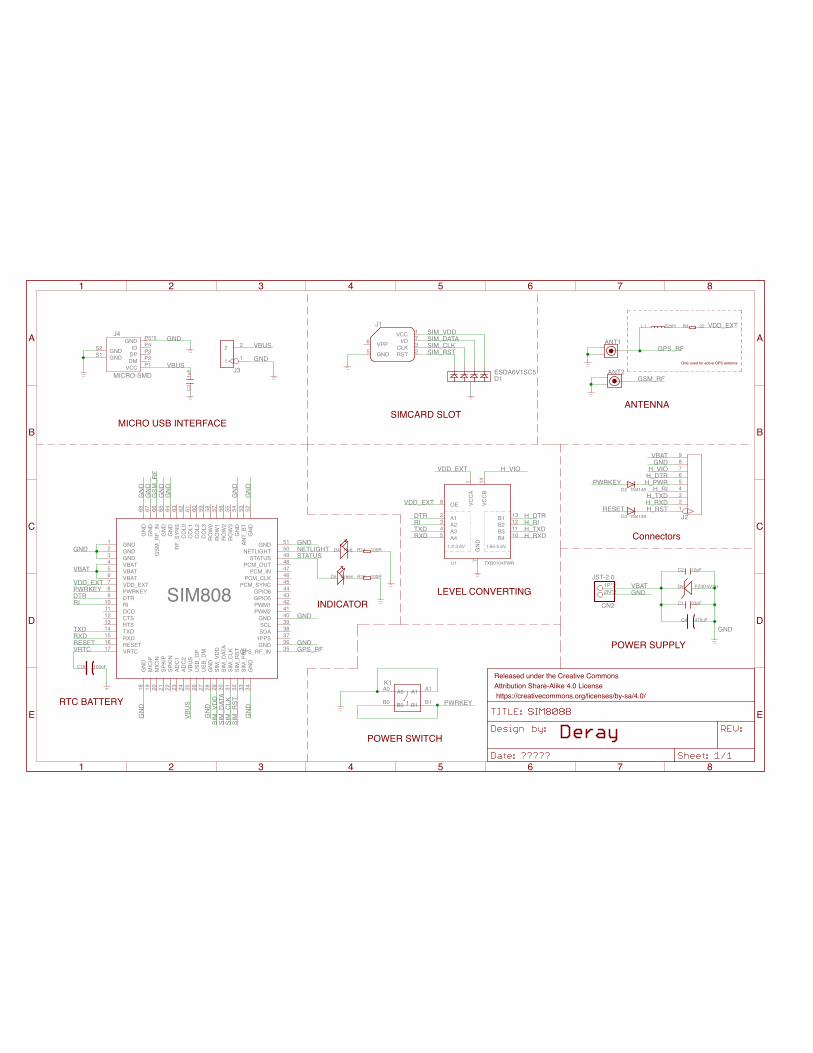
Below is the GPRS/GSM/GPS module that team child safetywill be using for voice communciation and GPS location.
Fig. 5: GSM/GPRS/GPS
Below is the Intel Edison microprocessor that team childsafety will be using for integrating all the features together.
Fig. 6: Intel Edison Chip
Below is the Intel Edison Board that team child safety willbe using for integrating all the features together.
Fig. 7: Intel Edison Board

13
Below is the working prototype of GPRS/GSM/GPS usingArduino UNO board.
Fig. 8: GSM/GPRS/GPS Working Prototype
XIV. CONCLUSION
This document has described our development towards awearable device that will provide parents and guardians peaceof mind as their children are out and about throughout theday by providing their location, status of their health, and amedium to communicate (via voice and text messaging). Webelieve that users of our product will benefit from the wealthof data our device captures and stores. As members of theengineering community it is our responsibility to utilize ourskillsets and knowledge obtained to better society. Childrenhave and will always be the key to our future as bred amongstthem will be our next great leaders and inventors and webelieve it is our duty to protect them and ensure their safety.With our combined engineering skillsets we believe our systemwill accomplish this task while also providing parents andguardians with peace of mind.

14
APPENDIX
REFERENCES
[1] N. C. for Missing and E. Children. (2015) Key facts. [Online]. Available: http://www.missingkids.com/KeyFacts[2] A. Willis. (2015) Youtuber coby persin societal experiment for children and parents. [Online]. Available: http://metro.co.uk/2015/08/11/
wheres-your-child-predator-test-shows-how-easy-it-is-to-kidnap-young-girls-5338083/[3] DIYmall. (2015) Diymall sim808 gps gsm gprs module for arduino. [Online]. Available: http://www.amazon.com/
Diymall-SIM808-GPRS-Module-Arduino/dp/B00Y20CRJG/ref=sr 1 1?ie=UTF8&qid=1448770608&sr=8-1&keywords=sim808[4] ——. (2015) Lonet - gsm/gprs/gps breakout. [Online]. Available: http://www.seeedstudio.com/wiki/LoNet - GSM/GPRS/GPS Breakout[5] J. Brains. (2015) Intellij idea. [Online]. Available: https://www.jetbrains.com/idea/[6] A. A. Huurdeman. (2003) The worldwide history of telecommunications. [Online]. Available: https://books.google.se/books?hl=sv&id=SnjGRDVIUL4C&
dq=GSM+1992&q=GSM+first#v=snippet&q=GSM%201992%20finnish&f=false[7] Google. (2015) Android studio. [Online]. Available: http://developer.android.com/tools/studio/index.html[8] (2003) Heart rate monitor. [Online]. Available: https://en.wikipedia.org/wiki/Heart rate monitor[9] (2015) Clock. [Online]. Available: https://en.wikipedia.org/wiki/Panic button
[10] Adafruit. (2015) Triple-axis accelerometer+magnetometer (compass) board - lsm303. [Online]. Available: http://www.adafruit.com/products/1120[11] (2015) Pedometer. [Online]. Available: https://en.wikipedia.org/wiki/Pedometer[12] Intel. (2015) Intel edison. [Online]. Available: http://www.intel.com/content/www/us/en/do-it-yourself/edison.html
15
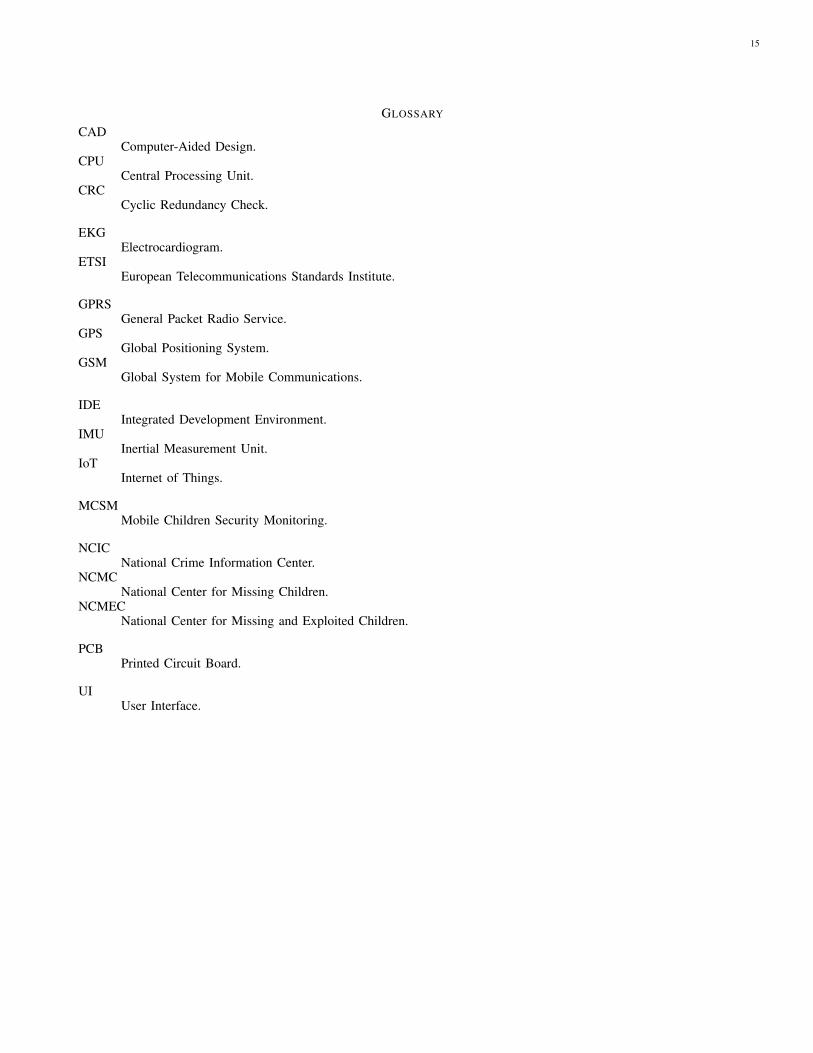
GLOSSARY
CADComputer-Aided Design.
CPUCentral Processing Unit.
CRCCyclic Redundancy Check.
EKGElectrocardiogram.
ETSIEuropean Telecommunications Standards Institute.
GPRSGeneral Packet Radio Service.
GPSGlobal Positioning System.
GSMGlobal System for Mobile Communications.
IDEIntegrated Development Environment.
IMUInertial Measurement Unit.
IoTInternet of Things.
MCSMMobile Children Security Monitoring.
NCICNational Crime Information Center.
NCMCNational Center for Missing Children.
NCMECNational Center for Missing and Exploited Children.
PCBPrinted Circuit Board.
UIUser Interface.

16
ACKNOWLEDGMENT
Team Child Safety would like to thank Dr. Dennis Dalhquist, Professor Russ Tatro, Dr. Fethi Belkhouche for all their help.Additionally, the authors would like to thank Dr. Fethi Belkhouche for his feedback and support regarding implementation
and design.
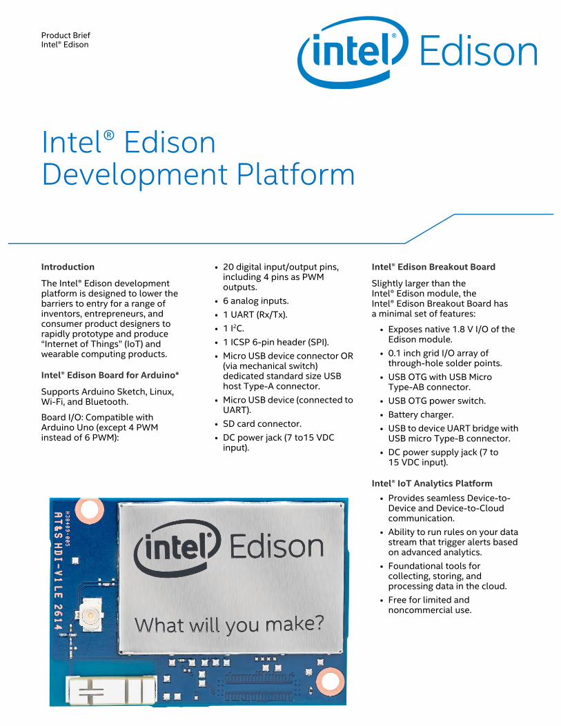
Product BriefIntel® Edison
Introduction
The Intel® Edison development platform is designed to lower the barriers to entry for a range of inventors, entrepreneurs, and consumer product designers to rapidly prototype and produce “Internet of Things” (IoT) and wearable computing products.
Intel® Edison Board for Arduino*
Supports Arduino Sketch, Linux, Wi-Fi, and Bluetooth.
Board I/O: Compatible with Arduino Uno (except 4 PWM instead of 6 PWM):
• 20 digital input/output pins, including 4 pins as PWM outputs.
• 6 analog inputs. • 1 UART (Rx/Tx). • 1 I2C. • 1 ICSP 6-pin header (SPI). • Micro USB device connector OR
(via mechanical switch) dedicated standard size USB host Type-A connector.
• Micro USB device (connected to UART).
• SD card connector. • DC power jack (7 to15 VDC
input).
Intel® Edison Breakout Board
Slightly larger than the Intel® Edison module, the Intel® Edison Breakout Board has a minimal set of features:
• Exposes native 1.8 V I/O of the Edison module.
• 0.1 inch grid I/O array of through-hole solder points.
• USB OTG with USB Micro Type-AB connector.
• USB OTG power switch. • Battery charger. • USB to device UART bridge with
USB micro Type-B connector. • DC power supply jack (7 to
15 VDC input).
Intel® IoT Analytics Platform
• Provides seamless Device-to-Device and Device-to-Cloud communication.
• Ability to run rules on your data stream that trigger alerts based on advanced analytics.
• Foundational tools for collecting, storing, and processing data in the cloud.
• Free for limited and noncommercial use.
Intel® Edison Development Platform
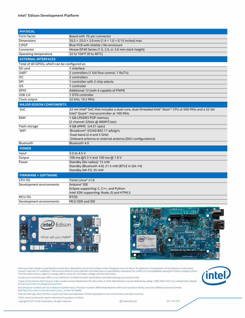
Intel® Edison Development Platform
Intel may make changes to specifications and product descriptions at any time, without notice. Designers must not rely on the absence or characteristics of any features or instructions marked “reserved” or “undefined”. Intel reserves these for future definition and shall have no responsibility whatsoever for conflicts or incompatibilities arising from future changes to them. The information here is subject to change without notice. Do not finalize a design with this information. Contact your local Intel sales office or your distributor to obtain the latest specifications and before placing your product order. Copies of documents which have an order number and are referenced in this document, or other Intel literature, may be obtained by calling 1-800-548-4725 or by visiting Intel’s website at http://www.intel.com/design/literature.htm. Intel processor numbers are not a measure of performance. Processor numbers differentiate features within each processor family, not across different processor families. See http://www.intel.com/products/processor_number for details. Intel, the Intel logo, Atom, Pentium, Quark, and Xeon are trademarks of Intel Corporation in the United States and other countries. *Other names and brands may be claimed as the property of others. Copyright © 2014 Intel Corporation. All rights reserved. Please Recycle 331179-001
PHYSICALForm factor Board with 70-pin connectorDimensions 35.5 × 25.0 × 3.9 mm (1.4 × 1.0 × 0.15 inches) maxC/M/F Blue PCB with shields / No enclosureConnector Hirose DF40 Series (1.5, 2.0, or 3.0 mm stack height)Operating temperature 32 to 104°F (0 to 40°C)
EXTERNAL INTERFACESTotal of 40 GPIOs, which can be configured as:SD card 1 interfaceUART 2 controllers (1 full flow control, 1 Rx/Tx) I2C 2 controllersSPI 1 controller with 2 chip selectsI2S 1 controllerGPIO Additional 12 (with 4 capable of PWM)USB 2.0 1 OTG controllerClock output 32 kHz, 19.2 MHz
MAJOR EDISON COMPONENTS SoC 22 nm Intel® SoC that includes a dual-core, dual-threaded Intel® Atom™ CPU at 500 MHz and a 32-bit
Intel® Quark™ microcontroller at 100 MHzRAM 1 GB LPDDR3 POP memory
(2 channel 32bits @ 800MT/sec)Flash storage 4 GB eMMC (v4.51 spec) WiFi Broadcom* 43340 802.11 a/b/g/n;
Dual-band (2.4 and 5 GHz) Onboard antenna or external antenna (SKU configurations)
Bluetooth Bluetooth 4.0
POWERInput 3.3 to 4.5 V Output 100 ma @3.3 V and 100 ma @ 1.8 VPower Standby (No radios): 13 mW
Standby (Bluetooth 4.0): 21.5 mW (BTLE in Q4-14)Standby (Wi-Fi): 35 mW
FIRMWARE + SOFTWARECPU OS Yocto Linux* v1.6Development environments Arduino* IDE
Eclipse supporting: C, C++, and PythonIntel XDK supporting: Node.JS and HTML5
MCU OS RTOS Development environments MCU SDK and IDE

1.2-3.6V 1.65-5.5V
33pF
10pF
1uF
100R
100R
100uF
22nH 22
ESDA6V1SC5
470uF
Red
Green
TXB0104PWR
1N4148
JST-2.0
1N4148
GND1GND2GND3VBAT4VBAT5VBAT6VDD_EXT7PWRKEY8DTR9RI10DCD11CTS12RTS13TXD14RXD15RESET16VRTC17
GN
D18
MIC
IP19
MIC
IN20
SPKI
P21
SPKI
N22
ADC
123
ADC
224
VBU
S25
USB
_DP
26U
SB_D
M27
GN
D28
SIM
_VD
D29
SIM
_DAT
A30
SIM
_CLK
31SI
M_R
ST32
SIM
_PR
E33
GN
D34
GPS_RF_IN 35GND 361PPS 37SDA 38SCL 39GND 40PWM2 41PWM1 42GPIO5 43GPIO6 44PCM_SYNC 45PCM_CLK 46PCM_IN 47PCM_OUT 48STATUS 49NETLIGHT 50GND 51
GN
D52
ANT_
BT53
GN
D54
RO
W3
55R
OW
256
RO
W1
57R
OW
058
CO
L359
CO
L260
CO
L161
CO
L062
RF_
SYN
S63
GN
D64
GN
D65
GSM
_RF_
IN66
GN
D67
GN
D68
C1
C2
C3
J1VCC 1
RST 2CLK 3GND5VPP6 I/O 7
K1A0A0 A1 A1
B0B0 B1 B1
ANT1
R14
R15
C18
ANT2
J2123456789
L1 R4
D1
C4
D8 PZ3D4V2H
J31 1
2 2
D4
D5
VCC
A1
A12A23A34A45
GN
D7
VCC
B14
B1 13B2 12B3 11B4 10
OE8
U1
D3
CN2
2N*21P*2
D2
VCC P1DM P2DP P3ID P4GND P5*5
GNDS1 GNDS2
J4
MICRO-SMD
VBAT
VBAT
VBAT
GND
GND
GND
GN
D
GND
GN
D
GN
D
GND
GND
GND
GN
D
GN
D
GN
DG
ND
GN
DG
ND
GND
GNDVBUS
VBU
S
VBUS
SIM
_VD
D
SIM_VDD
SIM
_DAT
A
SIM_DATA
SIM
_CLK
SIM_CLK
SIM
_RST
SIM_RST
PWRKEY
PWRKEY
PWRKEY
GPS_RF
GPS_RF
GSM
_RF
GSM_RF
VRTC
VDD_EXT
VDD_EXT
VDD_EXT
VDD_EXT
TXD
TXD
RXD
RXD
RI
RI
RESET
RESET
H_VIOH_VIO
H_TXD
H_TXD
H_RXD
H_RXD
DTR
DTRH_RST
H_PWRH_DTR
H_DTR
H_RI
H_RI
NETLIGHTSTATUS
POWER SUPPLY
MICRO USB INTERFACESIMCARD SLOT
POWER SWITCH
ANTENNA
INDICATOR
RTC BATTERY
LEVEL CONVERTING
Connectors
Only used for active GPS antenna
A
B
C
D
E
1 2 3 4 5 6 7 8
A
B
C
D
E
1 2 3 4 5 6 7 8
Released under the Creative CommonsAttribution Share-Alike 4.0 License https://creativecommons.org/licenses/by-sa/4.0/
SIM808

SIM808_Hardware Design_V1.00
Smart Machine Smart Decision
SIM808_Hardware Design_V1.00 2014.03.27 2
Document Title SIM808_Hardware_Design_V1.00
Version 1.00
Date 2014-03-27
Status Release
Document Control ID SIM808_Hardware Design
General Notes SIMCom offers this information as a service to its customers, to support application and engineering efforts that use the products designed by SIMCom. The information provided is based upon requirements specifically provided to SIMCom by the customers. SIMCom has not undertaken any independent search for additional relevant information, including any information that may be in the customer’s possession. Furthermore, system validation of this product designed by SIMCom within a larger electronic system remains the responsibility of the customer or the customer’s system integrator. All specifications supplied herein are subject to change. Copyright This document contains proprietary technical information which is the property of SIMCom Limited, copying of this document and giving it to others and the using or communication of the contents thereof, are forbidden without express authority. Offenders are liable to the payment of damages. All rights reserved in the event of grant of a patent or the registration of a utility model or design. All specification supplied herein are subject to change without notice at any time. Copyright © Shanghai SIMCom Wireless Solutions Ltd. 2014

Smart Machine Smart Decision
SIM808_Hardware Design_V1.00 2014.03.27 3
Contents
Contents.................................................................................................................................................................... 3
Version History ........................................................................................................................................................ 9
1 Introduction..................................................................................................................................................... 10
2 SIM808 Overview ........................................................................................................................................... 10 2.1 SIM808 Key Features............................................................................................................................. 10 2.2 Operating Modes .................................................................................................................................... 13 2.3 SIM808 Functional Diagram.................................................................................................................. 14
3 Package Information ...................................................................................................................................... 15 3.1 Pin out Diagram...................................................................................................................................... 15 3.2 Pin Description ....................................................................................................................................... 16 3.3 Package Dimensions............................................................................................................................... 18
4 GSM Application Interface ............................................................................................................................ 20 4.1 Power Supply.......................................................................................................................................... 20
4.1.1 Power Supply Pin................................................................................................................................ 21 4.1.2 Monitoring Power Supply ................................................................................................................... 22
4.2 Power on/down SIM808......................................................................................................................... 22 4.2.1 Power on SIM808 ............................................................................................................................... 22 4.2.2 Power down SIM808........................................................................................................................... 24 4.2.3 Reset Function..................................................................................................................................... 25
4.3 Power Saving Mode................................................................................................................................ 26 4.3.1 Function Mode .................................................................................................................................... 27 4.3.2 Sleep Mode (AT+CSCLK=1) ............................................................................................................. 27 4.3.3 Wake Up SIM808 from Sleep Mode (AT+CSCLK=1) ...................................................................... 27
4.4 Charging Interface .................................................................................................................................. 28 4.4.1 Battery Pack Characteristics................................................................................................................ 28 4.4.2 Recommended Battery Pack ............................................................................................................... 28 4.4.3 Implemented Charging Technique ...................................................................................................... 29 4.4.4 Operating Modes during Charging...................................................................................................... 29 4.4.5 Charger Requirements......................................................................................................................... 30
4.5 RTC Backup ........................................................................................................................................... 30 4.6 Serial Port and USB Interface ................................................................................................................ 31
4.6.1 Function of Serial Port ........................................................................................................................ 32 4.6.2 Serial Port............................................................................................................................................ 32 4.6.3 USB Interface...................................................................................................................................... 34 4.6.4 Software Upgrade and Debug ............................................................................................................. 35
4.7 RI Behaviors........................................................................................................................................... 35 4.8 Audio Interfaces ..................................................................................................................................... 36
4.8.1 Speaker Interface Configuration ......................................................................................................... 37 4.8.2 Microphone Interfaces Configuration ................................................................................................. 37 4.8.3 Audio Electronic Characteristics......................................................................................................... 38 4.8.4 TDD .................................................................................................................................................... 38
4.9 Bluetooth ................................................................................................................................................ 39

Smart Machine Smart Decision
SIM808_Hardware Design_V1.00 2014.03.27 4
4.9.1 Antenna Interface ................................................................................................................................ 39 4.10 SIM Card Interface ................................................................................................................................. 39
4.10.1 SIM Card Application...................................................................................................................... 40 4.10.2 SIM Card Design Consideration...................................................................................................... 41 4.10.3 Design Considerations for SIM Card Holder................................................................................... 41
4.11 PCM Interface ........................................................................................................................................ 43 4.11.1 PCM Multiplex Function ................................................................................................................. 43 4.11.2 PCM Interface.................................................................................................................................. 44 4.11.3 LCD Display/SPI Interface.............................................................................................................. 44 4.11.4 SD Card Interface ............................................................................................................................ 45
4.12 Keypad Interface .................................................................................................................................... 45 4.13 I2C BUS ................................................................................................................................................. 47
4.13.1 General Purpose Input/Output (GPIO) ............................................................................................ 48 4.14 ADC........................................................................................................................................................ 48 4.15 PWM ...................................................................................................................................................... 49 4.16 Network Status Indication ...................................................................................................................... 50 4.17 Operating Status Indication .................................................................................................................... 50 4.18 RF Synchronization Signal..................................................................................................................... 51 4.19 Antenna Interface ................................................................................................................................... 51
5 GPS Application Interface ............................................................................................................................. 52 5.1 GPS Operating Modes ............................................................................................................................ 52 5.2 GPS Power on/down Scenarios .............................................................................................................. 53
5.2.1 Power on GPS engine.......................................................................................................................... 53 5.2.2 Power down GPS engine..................................................................................................................... 53
5.3 GPS Antenna Interface ........................................................................................................................... 53 5.3.1 GPS Antenna Interface........................................................................................................................ 53 5.3.2 GPS Antenna Choice Consideration ................................................................................................... 53
6 Electrical, Reliability and Radio Characteristics......................................................................................... 54 6.1 Absolute Maximum Ratings................................................................................................................... 54 6.2 Recommended Operating Conditions..................................................................................................... 55 6.3 Digital Interface Characteristics ............................................................................................................. 55 6.4 SIM Card Interface Characteristics ........................................................................................................ 55 6.5 SIM_VDD Characteristics...................................................................................................................... 56 6.6 VDD_EXT Characteristics ..................................................................................................................... 56 6.7 VRTC Characteristics ............................................................................................................................. 56 6.8 Current Consumption (VBAT = 4V, GPS engine is powered down)...................................................... 56 6.9 Electro-Static Discharge ......................................................................................................................... 57 6.10 Radio Characteristics.............................................................................................................................. 58
6.10.1 Module RF Output Power................................................................................................................ 58 6.10.2 Module RF Receive Sensitivity ....................................................................................................... 59 6.10.3 Module Operating Frequencies........................................................................................................ 60
7 Manufacturing ................................................................................................................................................ 61 7.1 Top and Bottom View of SIM808........................................................................................................... 61 7.2 Typical Solder Reflow Profile ................................................................................................................ 61 7.3 The Moisture Sensitivity Level .............................................................................................................. 62 7.4 Baking Requirements ............................................................................................................................. 62
Appendix ................................................................................................................................................................ 63
Smart Machine Smart Decision
SIM808_Hardware Design_V1.00 2014.03.27 5
A. Related Documents.......................................................................................................................................... 63 B. Terms and Abbreviations ................................................................................................................................. 64 C. Safety Caution ................................................................................................................................................. 65
Table Index
TABLE 1: SIM808 GSM/GPRS ENGINE KEY FEATURES ......................................................................................... 10 TABLE 2: GPS ENGINE PERFORMANCE ................................................................................................................... 12 TABLE 3: CODING SCHEMES AND MAXIMUM NET DATA RATES OVER AIR INTERFACE ............................ 12 TABLE 4: OVERVIEW OF OPERATING MODES........................................................................................................ 13 TABLE 5: PIN DESCRIPTION ....................................................................................................................................... 16 TABLE 6: RECOMMENDED ZENER DIODE .............................................................................................................. 20 TABLE 7: ELECTRONIC CHARACTERISTIC OF THE RESET PIN.......................................................................... 26 TABLE 8: THE CURRENT CONSUMPTION OF FUNCTION MODES (BS-PA-MFRMS=5) ................................... 27 TABLE 9: SPECIFICATION OF RECOMMENDED BATTERY PACK........................................................................ 28 TABLE 10: SERIAL PORT AND USB PIN DEFINITION ............................................................................................. 31 TABLE 11: SERIAL PORT CHARACTERISTICS......................................................................................................... 31 TABLE 12: SERIAL PORT CHARACTERISTICS......................................................................................................... 34 TABLE 13: RI BEHAVIORS ........................................................................................................................................... 35 TABLE 14: AUDIO INTERFACE DEFINITION............................................................................................................ 36 TABLE 15: MICROPHONE INPUT CHARACTERISTICS........................................................................................... 38 TABLE 16: AUDIO OUTPUT CHARACTERISTICS .................................................................................................... 38 TABLE 17: SIM PIN DEFINITION................................................................................................................................. 40 TABLE 18: PIN DESCRIPTION (MOLEX SIM CARD HOLDER) .............................................................................. 42 TABLE 19: PIN DESCRIPTION (AMPHENOL SIM CARD HOLDER)....................................................................... 42 TABLE 20: PCM PIN DEFINITION ............................................................................................................................... 43 TABLE 21: PCM PIN SPECIFICATION......................................................................................................................... 43 TABLE 22: PCM MULTIPLEX FUNCTION.................................................................................................................. 43 TABLE 23: PIN DEFINITION OF THE KEYPAD INTERFACE................................................................................... 47 TABLE 24: KEYPAD MULTIPLEX FUNCTION........................................................................................................... 47 TABLE 25: PIN DEFINITION OF THE I2C................................................................................................................... 48 TABLE 26: I2C MULTIPLEX FUNCTION .................................................................................................................... 48 TABLE 27: PIN DEFINITION OF THE GPIO................................................................................................................ 48 TABLE 28: PIN DEFINITION OF THE ADC................................................................................................................. 48 TABLE 29: ADC SPECIFICATION ................................................................................................................................ 49 TABLE 30: PIN DEFINITION OF THE PWM ............................................................................................................... 49 TABLE 31: BUZZER OUTPUT CHARACTERISTICS ................................................................................................. 49 TABLE 32: PWM MULTIPLEX FUNCTION................................................................................................................. 49 TABLE 33: PIN DEFINITION OF THE NETLIGHT ..................................................................................................... 50 TABLE 34: STATUS OF THE NETLIGHT PIN.............................................................................................................. 50 TABLE 35: PIN DEFINITION OF THE STATUS........................................................................................................... 50 TABLE 36: DEFINITION OF THE RF_SYNC PIN........................................................................................................ 51 TABLE 37: AT COMMANDS FOR GPS FUNCTION.................................................................................................... 52 TABLE 38: ABSOLUTE MAXIMUM RATINGS........................................................................................................... 54 TABLE 39: RECOMMENDED OPERATING CONDITIONS ....................................................................................... 55 TABLE 40: DIGITAL INTERFACE CHARACTERISTICS ........................................................................................... 55 TABLE 41: SIM CARD INTERFACE CHARACTERISTICS........................................................................................ 55 TABLE 42: SIM_VDD CHARACTERISTICS................................................................................................................ 56

Smart Machine Smart Decision
SIM808_Hardware Design_V1.00 2014.03.27 6
TABLE 43: VDD_EXT CHARACTERISTICS ............................................................................................................... 56 TABLE 44: VRTC CHARACTERISTICS ....................................................................................................................... 56 TABLE 45: GSM CURRENT CONSUMPTION*............................................................................................................ 56 TABLE 46: THE ESD CHARACTERISTICS (TEMPERATURE: 25, HUMIDITY: 45 %) ....................................... 57 TABLE 47: SIM808 GSM 900 AND GSM 850 CONDUCTED RF OUTPUT POWER ................................................ 58 TABLE 48: SIM808 DCS 1800 AND PCS 1900 CONDUCTED RF OUTPUT POWER............................................... 58 TABLE 49: SIM808 CONDUCTED RF RECEIVE SENSITIVITY ............................................................................... 59 TABLE 50: SIM808 OPERATING FREQUENCIES....................................................................................................... 60 TABLE 51: MOISTURE CLASSIFICATION LEVEL AND FLOOR LIFE ................................................................... 62 TABLE 52: BAKING REQUIREMENTS ....................................................................................................................... 62 TABLE 53: RELATED DOCUMENTS ........................................................................................................................... 63 TABLE 54: TERMS AND ABBREVIATIONS................................................................................................................ 64 TABLE 55: SAFETY CAUTION..................................................................................................................................... 65
Smart Machine Smart Decision
SIM808_Hardware Design_V1.00 2014.03.27 7
Figure Index
FIGURE 1: SIM808 FUNCTIONAL DIAGRAM ........................................................................................................... 14 FIGURE 2: SIM808 PIN OUT DIAGRAM (TOP VIEW) ............................................................................................... 15 FIGURE 3: DIMENSIONS OF SIM808(UNIT: MM)................................................................................................ 18 FIGURE 4: RECOMMENDED PCB FOOTPRINT OUTLINE(UNIT: MM)............................................................ 19 FIGURE 5: REFERENCE CIRCUIT OF THE VBAT INPUT......................................................................................... 20 FIGURE 6: REFERENCE CIRCUIT OF THE LDO POWER SUPPLY......................................................................... 20 FIGURE 7: REFERENCE CIRCUIT OF THE DC-DC POWER SUPPLY..................................................................... 21 FIGURE 8: VBAT VOLTAGE DROP DURING TRANSMIT BURST........................................................................... 21 FIGURE 9: THE MINIMAL VBAT VOLTAGE REQUIREMENT AT VBAT DROP .................................................... 22 FIGURE 10: POWERED ON/DOWN MODULE USING TRANSISTOR..................................................................... 22 FIGURE 11: POWERED ON/DOWN MODULE USING BUTTON ............................................................................. 22 FIGURE 12: TIMING OF POWER ON MODULE......................................................................................................... 23 FIGURE 13: TIMING OF POWER ON MODULE......................................................................................................... 23 FIGURE 14: TIMING OF POWER DOWN SIM808 BY PWRKEY.............................................................................. 24 FIGURE 15: RESET CIRCUIT........................................................................................................................................ 26 FIGURE 16: RESET TIMING SEQUENCE.................................................................................................................... 26 FIGURE 17: SIM808 WITH BATTERY CHARGER AND PACK CONNECTION....................................................... 28 FIGURE 18: RTC SUPPLY FROM CAPACITOR........................................................................................................... 30 FIGURE 19: RTC SUPPLY FROM NON-CHARGEABLE BATTERY ......................................................................... 30 FIGURE 20: RTC SUPPLY FROM RECHARGEABLE BATTERY .............................................................................. 30 FIGURE 21: SEIKO XH414H-IV01E CHARGE-DISCHARGE CHARACTERISTIC ................................................. 31 FIGURE 22: CONNECTION OF THE SERIAL PORT................................................................................................... 32 FIGURE 23: LEVEL CONVERTING BY RESISTOR.................................................................................................... 33 FIGURE 24: ISOLATION CIRCUIT BY DIODES ......................................................................................................... 33 FIGURE 25: TX LEVEL CONVERTING BY TRANSISTOR........................................................................................ 33 FIGURE 26: RX LEVEL CONVERTING BY TRANSISTOR ....................................................................................... 34 FIGURE 27: USB REFERENCE CIRCUIT .................................................................................................................... 34 FIGURE 28: RI BEHAVIOUR OF VOICE CALLING AS A RECEIVER...................................................................... 35 FIGURE 29: RI BEHAVIOUR OF DATA CALLING AS A RECEIVER........................................................................ 36 FIGURE 30: RI BEHAVIOUR OF URC OR RECEIVE SMS ........................................................................................ 36 FIGURE 31: RI BEHAVIOUR AS A CALLER ............................................................................................................... 36 FIGURE 32: SPEAKER REFERENCE CIRCUIT .......................................................................................................... 37 FIGURE 33: SPEAKER WITH AMPLIFIER REFERENCE CIRCUIT ......................................................................... 37 FIGURE 34 : MICROPHONE REFERENCE CIRCUIT................................................................................................. 37 FIGURE 35: BLUETOOTH ANTENNA MATCHING CIRCUIT ................................................................................. 39 FIGURE 36: REFERENCE CIRCUIT OF THE 8-PIN SIM CARD HOLDER............................................................... 40 FIGURE 37: REFERENCE CIRCUIT OF THE 6-PIN SIM CARD HOLDER............................................................... 40 FIGURE 38: MOLEX 91228 SIM CARD HOLDER ...................................................................................................... 41 FIGURE 39: AMPHENOL C707 10M006 5122 SIM CARD HOLDER......................................................................... 42 FIGURE 40: PCM REFERENCE CIRCUIT.................................................................................................................... 44 FIGURE 41: LCD REFERENCE CIRCUIT .................................................................................................................... 44 FIGURE 42: SD REFERENCE CIRCUIT....................................................................................................................... 45 FIGURE 43: TRADITIONAL KEYPAD REFERENCE CIRCUIT................................................................................. 45 FIGURE 44: EXTENDED KEYPAD REFERENCE CIRCUIT ...................................................................................... 46 FIGURE 45: ENHANCE THE ESD PERFORMANCE OF KEYPAD CIRCUIT........................................................... 46 FIGURE 46: KEYPAD DETECTED ............................................................................................................................... 47 FIGURE 47: REFERENCE CIRCUIT OF PWM DRIVE BUZZER ............................................................................... 49
Smart Machine Smart Decision
SIM808_Hardware Design_V1.00 2014.03.27 8
FIGURE 48: REFERENCE CIRCUIT OF NETLIGHT .................................................................................................. 50 FIGURE 49: RF_SYNC SIGNAL DURING TRANSMIT BURST ................................................................................ 51 FIGURE 50: GSM ANTENNA MATCHING CIRCUIT ................................................................................................. 51 FIGURE 51: GPS ANTENNA MATCHING CIRCUIT................................................................................................... 53 FIGURE 52: TOP AND BOTTOM VIEW OF SIM808 ................................................................................................... 61 FIGURE 53: TYPICAL SOLDER REFLOW PROFILE ................................................................................................. 61

Smart Machine Smart Decision
SIM808_Hardware Design_V2.00 8 2014.03.27
Version History
Date Version Description of change Author
2014-03-27 1.00 Origin ShengWu.Sun Xuegang.Wang
Smart Machine Smart Decision
SIM808_Hardware Design_V1.00 2014.03.27 10
1 Introduction
This document describes SIM808 hardware interface in great detail. This document can help user to quickly understand SIM808 interface specifications, electrical and mechanical details. With the help of this document and other SIM808 application notes, user guide, users can use SIM808 to design various applications quickly.
2 SIM808 Overview
Designed for global market, SIM808 is integrated with a high performance GSM/GPRS engine, a GPS engine and a BT engine. The GSM/GPRS engine is a quad-band GSM/GPRS module that works on frequencies GSM 850MHz, EGSM 900MHz, DCS 1800MHz and PCS 1900MHz. SIM808 features GPRS multi-slot class 12/ class 10 (optional) and supports the GPRS coding schemes CS-1, CS-2, CS-3 and CS-4. The GPS solution offers best- in-class acquisition and tracing sensitivity, Time-To-First-Fix (TTFF) and accuracy. With a tiny configuration of 24*24*2.6mm, SIM808 can meet almost all the space requirements in user applications, such as M2M, smart phone, PDA, tracker and other mobile devices. SIM808 has 68 SMT pads, and provides all hardware interfaces between the module and customers’ boards.
Support 4*4*2 keypads. One full modem serial port. One USB, the USB interfaces can debug, download software. Audio channels which include a microphone input and a receiver output. One SIM card interface. Charging interface. Programmable general purpose input and output. Support Bluetooth function. Support PWM and ADC. PCM/SPI/SD card interface, only one function can be accessed synchronously. (Default function is PCM).
SIM808 is designed with power saving technique so that the current consumption is as low as 1mA in sleep mode (GPS engine is powered down). SIM808 integrates TCP/IP protocol and extended TCP/IP AT commands which are very useful for data transfer applications. For details about TCP/IP applications, please refer to document [2].
2.1 SIM808 Key Features
Table 1: SIM808 GSM/GPRS engine key features
Feature Implementation
Power supply 3.4V ~ 4.4V
Power saving Typical power consumption in sleep mode is 1mA ( BS-PA-MFRMS=9, GPS engine is powered down )
Charging Supports charging control for Li-Ion battery
Frequency bands SIM808 Quad-band: GSM 850, EGSM 900, DCS 1800, PCS 1900. SIM808
Smart Machine Smart Decision
SIM808_Hardware Design_V1.00 2014.03.27 11
can search the 4 frequency bands automatically. The frequency bands also can be set by AT command “AT+CBAND”. For details, please refer to document [1].
Compliant to GSM Phase 2/2+
Transmitting power Class 4 (2W) at GSM 850 and EGSM 900 Class 1 (1W) at DCS 1800 and PCS 1900
GPRS connectivity GPRS multi-slot class 12(default) GPRS multi-slot class 1~12 (optional)
Temperature range Normal operation: -40 ~ +85 Storage temperature -45~ +90
Data GPRS
GPRS data downlink transfer: max. 85.6 kbps GPRS data uplink transfer: max. 85.6 kbps Coding scheme: CS-1, CS-2, CS-3 and CS-4 PAP protocol for PPP connect Integrate the TCP/IP protocol. Support Packet Broadcast Control Channel (PBCCH) CSD transmission rates:2.4,4.8,9.6,14.4 kbps
CSD Support CSD transmission
USSD Unstructured Supplementary Services Data (USSD) support
SMS MT, MO, CB, Text and PDU mode SMS storage: SIM card
SIM interface Support SIM card: 1.8V, 3V
External antenna Antenna pad
Audio features
Speech codec modes: Half Rate (ETS 06.20) Full Rate (ETS 06.10) Enhanced Full Rate (ETS 06.50 / 06.60 / 06.80) Adaptive multi rate (AMR) Echo Cancellation Noise Suppression
Serial port and USB interface
Serial port: Full modem interface with status and control lines, unbalanced,
asynchronous. 1200bps to 115200bps. Can be used for AT commands or data stream. Support RTS/CTS hardware handshake and software ON/OFF flow control. Multiplex ability according to GSM 07.10 Multiplexer Protocol. Autobauding supports baud rate from 1200 bps to 115200bps.
USB interface: Can be used as debugging and firmware upgrading.
Phonebook management Support phonebook types: SM, FD, LD, RC, ON, MC.
SIM application toolkit GSM 11.14 Release 99
Real time clock Support RTC
Alarm function Can be set by AT command
Physical characteristics Size: 24*24*2.6mm Weight: 3.5g

Smart Machine Smart Decision
SIM808_Hardware Design_V1.00 2014.03.27 12
Firmware upgrade Firmware upgrading by USB interface.
Table 2: GPS engine Performance
Performance Parameter Description
Min Type Max Unit
Horizontal Position Accuracy(1)
Autonomous <2.5 m
Without Aid 0.1 m/s Velocity Accuracy(2) DGPS 0.05 m/s
Without Aid 0.1 m/s2 Acceleration Accuracy DGPS 0.05 m/s2
Timing Accuracy 10 nS
Maximum Altitude 18000 m
Maximum Velocity 515 m/s
Dynamic Performance
Maximum Acceleration 4 G
Hot start 1 s
Warm start 28 s
Time To First Fix(3)
Cold start 30 s
Autonomous acquisition(cold start)
-147 dBm
Re-acquisition -159 dBm
Sensitivity
Tracking -165 dBm
Channels 22/66
Update rate 5 Hz
Tracking L1, CA Code
Receiver
Protocol support NMEA
Acquisition 42 mA Power consumption(4) Continuous tracking 24 mA
(1) 50% 24hr static, -130dBm (2) 50% at 30m/s (3) GPS signal level: -130dBm (4) Single Power supply 3.8V@-130dBm,GSM IDLE
Table 3: Coding schemes and maximum net data rates over air interface
Coding scheme 1 timeslot 2 timeslot 4 timeslot
CS-1 9.05kbps 18.1kbps 36.2kbps
CS-2 13.4kbps 26.8kbps 53.6kbps
CS-3 15.6kbps 31.2kbps 62.4kbps
CS-4 21.4kbps 42.8kbps 85.6kbps

Smart Machine Smart Decision
SIM808_Hardware Design_V1.00 2014.03.27 13
2.2 Operating Modes
The table below summarizes the various operating modes of SIM808.
Table 4: Overview of operating modes
Mode Function
GSM/GPRS SLEEP
Module will automatically go into sleep mode if the conditions of sleep mode are enabling and there is no on air and no hardware interrupt (such as GPIO interrupt or data on serial port). In this case, the current consumption of module will reduce to the minimal level. In sleep mode, the module can still receive paging message and SMS.
GSM IDLE
Software is active. Module registered to the GSM network, and the module is ready to communicate.
GSM TALK
Connection between two subscribers is in progress. In this case, the power consumption depends on network settings such as DTX off/on, FR/EFR/HR, hopping sequences, antenna.
GPRS STANDBY
Module is ready for GPRS data transfer, but no data is currently sent or received. In this case, power consumption depends on network settings and GPRS configuration.
GPRS DATA
There is GPRS data transfer (PPP or TCP or UDP) in progress. In this case, power consumption is related with network settings (e.g. power control level); uplink/downlink data rates and GPRS configuration (e.g. used multi-slot settings).
Normal operation
Charge The mode support charge function (Default is not support).
Power down
Normal power down by sending the AT command “AT+CPOWD=1” or using the PWRKEY. The power management unit shuts down the power supply for the baseband part of the module, and only the power supply for the RTC is remained. Software is not active. The serial port is not accessible. Power supply (connected to VBAT) remains applied.
Minimum functionality mode
AT command “AT+CFUN” can be used to set the module to a minimum functionality mode without removing the power supply. In this mode, the RF part of the module will not work or the SIM card will not be accessible, or both RF part and SIM card will be closed, and the serial port is still accessible. The power consumption in this mode is lower than normal mode.
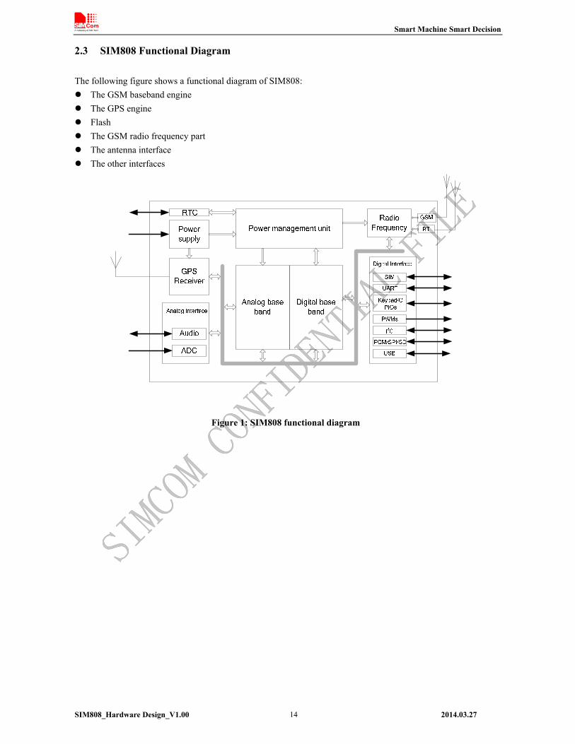
Smart Machine Smart Decision
2.3 SIM808 Functional Diagram
The following figure shows a functional diagram of SIM808: The GSM baseband engine The GPS engine Flash The GSM radio frequency part The antenna interface The other interfaces
Figure 1: SIM808 functional diagram
SIM808_Hardware Design_V1.00 2014.03.27 14
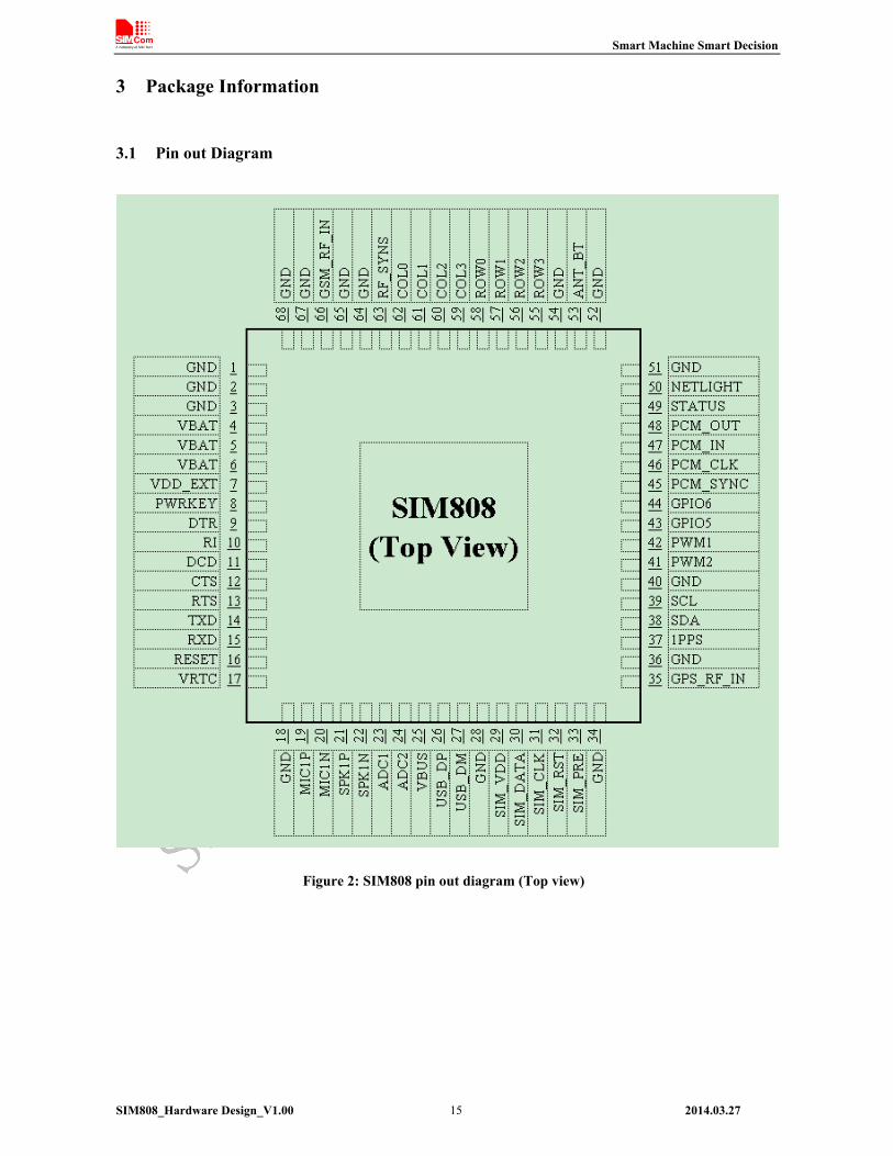
Smart Machine Smart Decision
3 Package Information
3.1 Pin out Diagram
Figure 2: SIM808 pin out diagram (Top view)
SIM808_Hardware Design_V1.00 2014.03.27 15
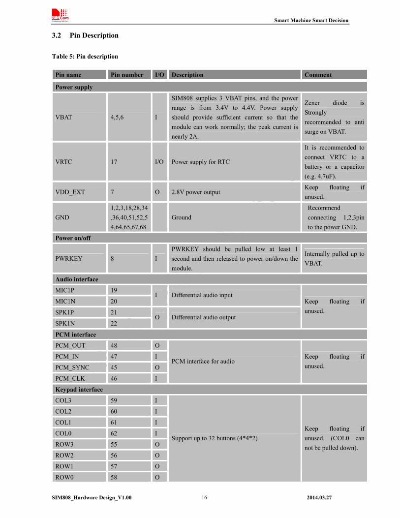
Smart Machine Smart Decision
SIM808_Hardware Design_V1.00 2014.03.27 16
3.2 Pin Description
Table 5: Pin description
Pin name Pin number I/O Description Comment
Power supply
VBAT 4,5,6 I
SIM808 supplies 3 VBAT pins, and the power range is from 3.4V to 4.4V. Power supply should provide sufficient current so that the module can work normally; the peak current is nearly 2A.
Zener diode is Strongly recommended to anti surge on VBAT.
VRTC 17 I/O Power supply for RTC
It is recommended to connect VRTC to a battery or a capacitor (e.g. 4.7uF).
VDD_EXT 7 O 2.8V power output Keep floating if unused.
GND 1,2,3,18,28,34,36,40,51,52,54,64,65,67,68
Ground Recommend connecting 1,2,3pin to the power GND.
Power on/off
PWRKEY 8 I PWRKEY should be pulled low at least 1 second and then released to power on/down the module.
Internally pulled up to VBAT.
Audio interface
MIC1P 19
MIC1N 20 I Differential audio input
SPK1P 21
SPK1N 22 O Differential audio output
Keep floating if unused.
PCM interface
PCM_OUT 48 O
PCM_IN 47 I
PCM_SYNC 45 O
PCM_CLK 46 I
PCM interface for audio Keep floating if unused.
Keypad interface
COL3 59 I
COL2 60 I
COL1 61 I
COL0 62 I
ROW3 55 O
ROW2 56 O
ROW1 57 O
ROW0 58 O
Support up to 32 buttons (4*4*2) Keep floating if unused. (COL0 can not be pulled down).
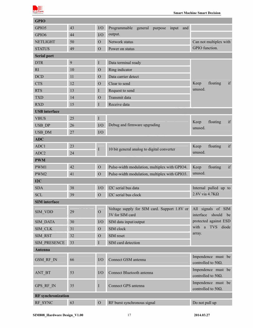
Smart Machine Smart Decision
SIM808_Hardware Design_V1.00 2014.03.27 17
GPIO
GPIO5 43 I/O
GPIO6 44 I/O
Programmable general purpose input and output.
NETLIGHT 50 O Network status
STATUS 49 O Power on status
Can not multiplex with GPIO function.
Serial port
DTR 9 I Data terminal ready
RI 10 O Ring indicator
DCD 11 O Data carrier detect
CTS 12 O Clear to send
RTS 13 I Request to send
TXD 14 O Transmit data
RXD 15 I Receive data
Keep floating if unused.
USB interface
VBUS 25 I
USB_DP 26 I/O
USB_DM 27 I/O
Debug and firmware upgrading Keep floating if unused.
ADC
ADC1 23
ADC2 24 I 10 bit general analog to digital converter
Keep floating if unused.
PWM
PWM1 42 O Pulse-width modulation, multiplex with GPIO4.
PWM2 41 O Pulse-width modulation, multiplex with GPIO3.
Keep floating if unused.
I2C
SDA 38 I/O I2C serial bus data
SCL 39 O I2C serial bus clock
Internal pulled up to 2.8V via 4.7KΩ
SIM interface
SIM_VDD 29 O Voltage supply for SIM card. Support 1.8V or 3V for SIM card
SIM_DATA 30 I/O SIM data input/output
SIM_CLK 31 O SIM clock
SIM_RST 32 O SIM reset
SIM_PRESENCE 33 I SIM card detection
All signals of SIM interface should be protected against ESD with a TVS diode array.
Antenna
GSM_RF_IN 66 I/O Connect GSM antenna Impendence must be controlled to 50Ω.
ANT_BT 53 I/O Connect Bluetooth antenna Impendence must be controlled to 50Ω.
GPS_RF_IN 35 I Connect GPS antenna Impendence must be controlled to 50Ω.
RF synchronization
RF_SYNC 63 O RF burst synchronous signal Do not pull up

Smart Machine Smart Decision
Other signal
RESET 16 I Reset input(Active low)
1PPS 37 I Time Mark outputs timing pulse related to receiver time
If unused, keep open.
3.3 Package Dimensions
Figure 3: Dimensions of SIM808(Unit: mm)
SIM808_Hardware Design_V1.00 2014.03.27 18
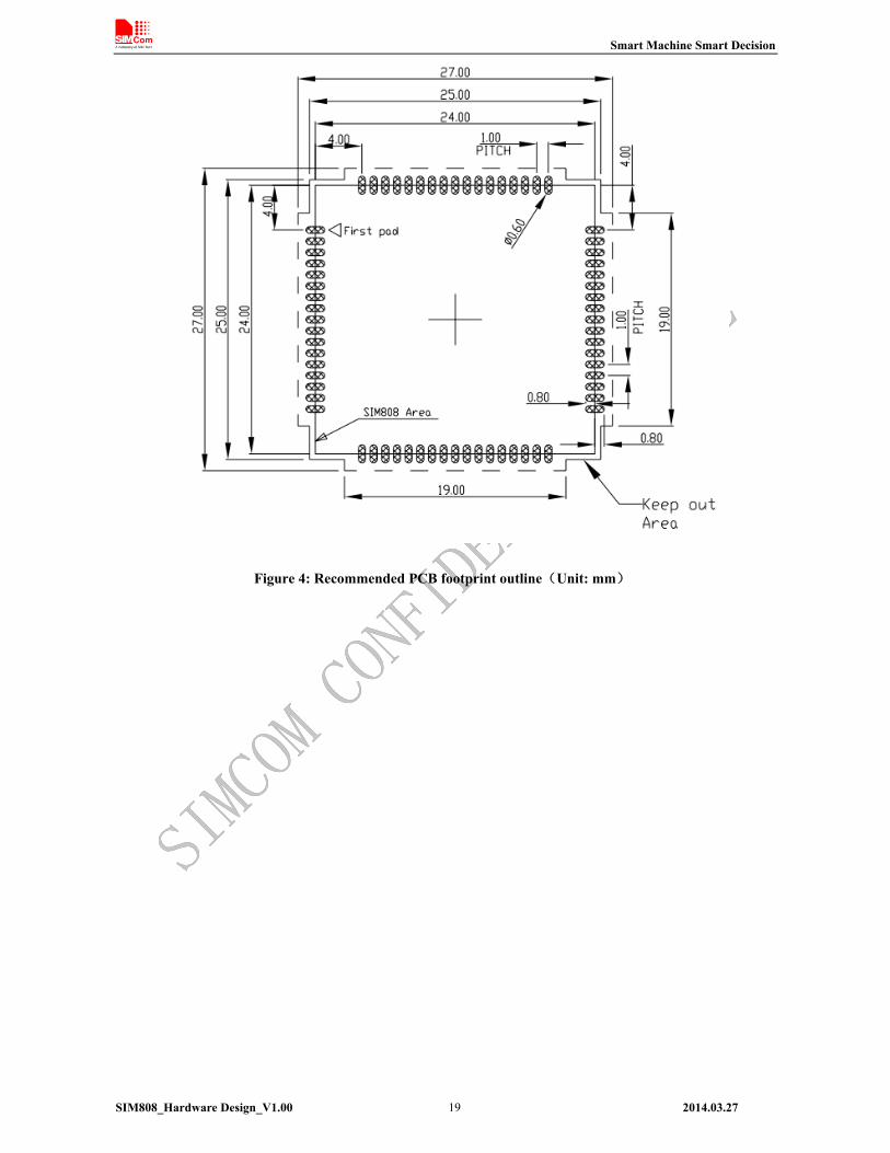
Smart Machine Smart Decision
Figure 4: Recommended PCB footprint outline(Unit: mm)
SIM808_Hardware Design_V1.00 2014.03.27 19

Smart Machine Smart Decision
4 GSM Application Interface
4.1 Power Supply
The power supply range of SIM808 is from 3.4V to 4.4V.Recommended voltage is 4.0V.The transmitting burst will cause voltage drop and the power supply must be able to provide sufficient current up to 2A. For the VBAT input, a bypass capacitor (low ESR) such as a 100 µF is strongly recommended. Increase the 33PF and 10PF capacitors can effectively eliminate the high frequency interference. A 5.1V/500mW Zener diode is strongly recommended, the diode can prevent chip from damaging by the voltage surge. These capacitors and Zener diode should be placed as close as possible to SIM808 VBAT pins.
Figure 5: Reference circuit of the VBAT input
Table 6: Recommended Zener diode
Vendor Part number Power(watts) Packages
1 On semi MMSZ5231BT1G 500mW SOD123
2 Prisemi PZ3D4V2H 500mW SOD323
3 Prisemi PZ5D4V2H 500mW SOD523
4 Vishay MMSZ4689-V 500mW SOD123
5 Crownpo CDZ55C5V1SM 500mW 0805
The following figure is the reference design of +5V input power supply. The designed output for the power supply is 4.1V, thus a linear regulator can be used.
SIM808_Hardware Design_V1.00 2014.03.27 20
Figure 6: Reference circuit of the LDO power supply
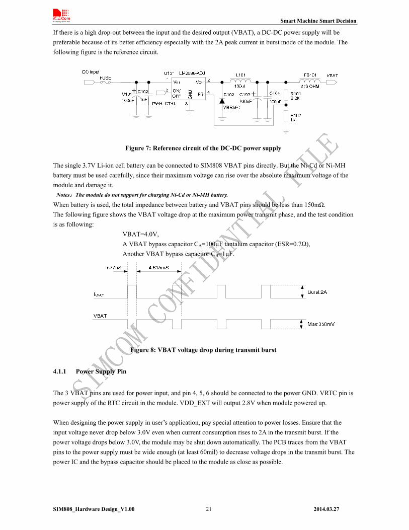
Smart Machine Smart Decision
If there is a high drop-out between the input and the desired output (VBAT), a DC-DC power supply will be preferable because of its better efficiency especially with the 2A peak current in burst mode of the module. The following figure is the reference circuit.
Figure 7: Reference circuit of the DC-DC power supply
The single 3.7V Li-ion cell battery can be connected to SIM808 VBAT pins directly. But the Ni-Cd or Ni-MH battery must be used carefully, since their maximum voltage can rise over the absolute maximum voltage of the module and damage it. Notes:The module do not support for charging Ni-Cd or Ni-MH battery. When battery is used, the total impedance between battery and VBAT pins should be less than 150mΩ. The following figure shows the VBAT voltage drop at the maximum power transmit phase, and the test condition is as following:
VBAT=4.0V, A VBAT bypass capacitor CA=100µF tantalum capacitor (ESR=0.7Ω), Another VBAT bypass capacitor CB=1µF.
Figure 8: VBAT voltage drop during transmit burst
4.1.1 Power Supply Pin
The 3 VBAT pins are used for power input, and pin 4, 5, 6 should be connected to the power GND. VRTC pin is power supply of the RTC circuit in the module. VDD_EXT will output 2.8V when module powered up. When designing the power supply in user’s application, pay special attention to power losses. Ensure that the input voltage never drop below 3.0V even when current consumption rises to 2A in the transmit burst. If the power voltage drops below 3.0V, the module may be shut down automatically. The PCB traces from the VBAT pins to the power supply must be wide enough (at least 60mil) to decrease voltage drops in the transmit burst. The power IC and the bypass capacitor should be placed to the module as close as possible.
SIM808_Hardware Design_V1.00 2014.03.27 21
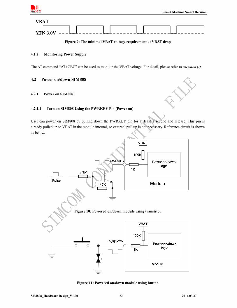
Smart Machine Smart Decision
SIM808_Hardware Design_V1.00 2014.03.27 22
Figure 9: The minimal VBAT voltage requirement at VBAT drop
4.1.2 Monitoring Power Supply
The AT command “AT+CBC” can be used to monitor the VBAT voltage. For detail, please refer to document [1].
4.2 Power on/down SIM808
4.2.1 Power on SIM808
4.2.1.1 Turn on SIM808 Using the PWRKEY Pin (Power on)
User can power on SIM808 by pulling down the PWRKEY pin for at least 1 second and release. This pin is already pulled up to VBAT in the module internal, so external pull up is not necessary. Reference circuit is shown as below.
Figure 10: Powered on/down module using transistor
Figure 11: Powered on/down module using button

Smart Machine Smart Decision
The power on scenarios is illustrated as following figure.
Figure 12: Timing of power on module
When power on procedure is completed, SIM808 will send following URC to indicate that the module is ready to operate at fixed baud rate.
RDY This URC does not appear when autobauding function is active.
Note: User can use AT command “AT+IPR=x” to set a fixed baud rate and save the configuration to non-volatile flash memory.
After the configuration is saved as fixed baud rate, the Code “RDY” should be received from the serial port every time when
SIM808 is powered on. For details, please refer to the chapter “AT+IPR” in document [1].
4.2.1.2 Turn on the SIM808 using the VBUS Signal
The SIM808 will be automatically turned on when a charger is connected to VBUS pin, the switched-off SIM808 of which VBAT pin voltage is greater than 3.4V. SIM808 will power up.
Figure 13: Timing of power on module
SIM808_Hardware Design_V1.00 2014.03.27 23

Smart Machine Smart Decision
4.2.2 Power down SIM808
SIM808 will be powered down in the following situations: Normal power down procedure: power down SIM808 by the PWRKEY pin. Normal power down procedure: power down SIM808 by AT command “AT+CPOWD=1”. Abnormal power down: over-voltage or under-voltage automatic power down. Abnormal power down: over-temperature or under-temperature automatic power down.
NOTE:The VBUS pin should not be charged, otherwise ,the module will not be powered down.
4.2.2.1 Power down SIM808 by the PWRKEY Pin
User can power down SIM808 by pulling down the PWRKEY pin for at least 1 second and release. Please refer to the power on circuit. The power down scenario is illustrated in following figure.
Figure 14: Timing of power down SIM808 by PWRKEY
This procedure makes the module log off from the network and allows the software to enter into a secure state to save data before completely shut down. Before the completion of the power down procedure, the module will send URC:
NORMAL POWER DOWN At this moment, AT commands can not be executed any more, and only the RTC is still active. Power down mode can also be indicated by STATUS pin, which is at low level at this time.
4.2.2.2 Power down SIM808 by AT Command
SIM808 can be powered down by AT command “AT+CPOWD=1”. This procedure makes the module log off from the network and allows the software to enter into a secure state to save data before completely shut down. Before the completion of the power down procedure, the module will send URC:
NORMAL POWER DOWN At this moment, AT commands can not be executed any more, and only the RTC is still active. Power down mode can also be indicated by STATUS pin, which is at low level at this time.
SIM808_Hardware Design_V1.00 2014.03.27 24

Smart Machine Smart Decision
SIM808_Hardware Design_V1.00 2014.03.27 25
For detail about the AT command “AT+CPOWD”, please refer to document [1]
4.2.2.3 Over-voltage or Under-voltage Power down
The module software monitors the VBAT voltage constantly. If the voltage ≤ 3.5V, the following URC will be reported: UNDER-VOLTAGE WARNNING If the voltage ≥ 4.3V, the following URC will be reported: OVER-VOLTAGE WARNNING If the voltage < 3.4V, the following URC will be reported, and the module will be automatically powered down.
UNDER-VOLTAGE POWER DOWN If the voltage > 4.4V, the following URC will be reported, and the module will be automatically powered down.
OVER-VOLTAGE POWER DOWN At this moment, AT commands can not be executed any more, and only the RTC is still active. Power down mode can also be indicated by STATUS pin, which is at low level at this time.
4.2.2.4 Over-temperature or Under-temperature Power down
The module will constantly monitor the temperature of the module, If the temperature > +80, the following URC will be reported: +CMTE: 1 If the temperature < -30, the following URC will be reported: +CMTE:-1 If the temperature > +85, the following URC will be reported, and the module will be automatically powered down. +CMTE: 2 If the temperature < -40, the following URC will be reported, and the module will be automatically powered down. +CMTE:-2 At this moment, AT commands can not be executed any more, and only the RTC is still active. Power down mode can also be indicated by STATUS pin, which is at low level at this time.
The AT command “AT+CMTE” could be used to read the temperature when the module is running. For details please refer to document [1].
4.2.3 Reset Function
SIM808 also has a RESET pin (pin 16) used to reset the module. This function is used as an emergency reset only when AT command “AT+CPOWD=1” and the POWER_ON pin has no effect. User can pull the RESET pin to ground, then the module will reset. This pin is already isolated in the module, so the external isolation is not necessary. Following figure is internal circuit of the RESET pin.
Smart Machine Smart Decision
Figure 15: Reset Circuit
The typical value of RESET pin high level is 2.8V, so for the 3V or 3.3V, customer could use MCU’s GPIO to driver this pin directly, resistor in serial the RESET signal could enhance the ESD performance but the value should not be too high, otherwise the level of RESET could be lower than threshold value; RESET hardware parameters can refer to the following table.
Table 7: Electronic characteristic of the RESET Pin
Pin name Symbol Min Typ Max Unit
VIH 2.7 2.8 2.9 V
VIL - - 0.6 V RESET
Tpull down 105 - mS
The reset scenarios are illustrated in the following figures.
Figure 16: Reset timing sequence
4.3 Power Saving Mode
User can control SIM808 module to enter or exit the sleep mode (AT+CSCLK=1) by DTR signal. When DTR is in high level and without interrupt (on air and hardware such as GPIO interrupt or data in serial port), SIM808 will enter sleep mode automatically. In this mode, SIM808 can still receive paging or SMS from network but the serial port is not accessible. Note: Customer must shut off the power supply of GPS, and then the AT commands about the power saving mode can be
executed correctly, and the current consumption will be lower.
SIM808_Hardware Design_V1.00 2014.03.27 26

Smart Machine Smart Decision
SIM808_Hardware Design_V1.00 2014.03.27 27
4.3.1 Function Mode
There are three functionality modes, which could be set by the AT command “AT+CFUN=<fun>”. The command provides the choice of the functionality levels <fun>=0, 1, 4.
AT+CFUN=0: minimum functionality. AT+CFUN=1: full functionality (default). AT+CFUN=4: flight mode (disable RF function).
Table 8: The current consumption of function modes (BS-PA-MFRMS=5)
<Fun> Current consumption(uA) (CSCLK=1)
0 869.5
1 1400
4 922.5
Minimum functionality mode minimizes the current consumption to the lowest level. If SIM808 is set to minimum functionality by “AT+CFUN=0”, the RF function and SIM card function will be disabled. In this case, the serial port is still accessible, but all AT commands correlative with RF function and SIM card function will not be accessible. For detailed information about the AT Command “AT+CFUN=<fun>”, please refer to document [1].
4.3.2 Sleep Mode (AT+CSCLK=1)
When the GPS function is shut off, user can control SIM808 module to enter or exit the sleep mode (AT+CSCLK=1) by DTR signal. When DTR is in high level and without interrupt (on air and hardware such as GPIO interrupt or data in serial port), SIM808 will enter sleep mode automatically. In this mode, SIM808 can still receive paging or SMS from network but the serial port is not accessible. Note: For SIM808, it requests to set AT command “AT+CSCLK=1” and ensure DTR at high level to enable the sleep mode ; the
default value is 0, which can not make the module to enter sleep mode. For more details please refer to document [1].
4.3.3 Wake Up SIM808 from Sleep Mode (AT+CSCLK=1)
When SIM808 is in sleep mode (AT+CSCLK=1), the following methods can wake up the module: Pull down DTR pin.
The serial port will be active after DTR pin is pulled to low level for about 50ms. Receive a voice or data call from network. Receive a SMS from network. Receive external interrupt Charge VBUS pin

Smart Machine Smart Decision
4.4 Charging Interface
SIM808 has integrated a charging circuit inside the module for Li-Ion batteries charging control, which make it very convenient for user’s applications that support battery charging. A common connection is shown in the following figure:
M oduleBattery
P ack
V B AT
V BU S
5V
Figure 17: SIM808 with battery charger and pack connection
4.4.1 Battery Pack Characteristics
SIM808 has optimized the charging algorithm for the Li-Ion battery that meets the characteristics listed below. The maximum charging voltage of the Li-Ion battery pack is 4.2V and the recommended capacity is
1100mAh. The Battery packs with more than 1100 mAh capacity will take more time for charging. The battery pack should have a protection circuit to avoid overcharging, deep discharging and over-current,
and the circuit should be insensitive to pulsed current. The internal resistance of the battery pack including protection circuit should be as low as possible. Its
recommended value does not exceed 150mΩ. The battery pack must be protected from reverse pole connection.
On the SIM808, the build-in circuit of the power management chipset monitors the supply voltage constantly. Once the Under-voltage is detected, the SIM808 will be powered down automatically.
4.4.2 Recommended Battery Pack
Following is the specification of recommended battery pack:
Table 9: Specification of recommended battery pack
Items Description
Battery type Li-ion
Manufacturer Jiade Energy Technology
Normal voltage 3.7V
Capacity NORMAL 1100mAh
Charge Voltage 4.200±0.050V
SIM808_Hardware Design_V1.00 2014.03.27 28
Smart Machine Smart Decision
SIM808_Hardware Design_V1.00 2014.03.27 29
Max Charge Current 1.0C
Charge Method CC / CV (Constant Current / Constant Voltage)
Max Discharge Current 1.0C (for continuous discharging mode)
Discharge Cut-off Voltage 3.0V/ cell
Internal resistance Initial≤150mΩ
4.4.3 Implemented Charging Technique
SIM808 has battery charging function, but default function is not support for charging, the customer should input AT command to enable charging function. There are two pins related to the battery charging function: there are VBUS, VBAT and pins. The VBUS Pin is driven by an external voltage (AC adapter or USB host), system can use this Pin to detect a charger supply and provide most charging current through SIM808 module to battery when charging is in fast charge state. VBAT pin gives charging current to external battery from SIM808 module. It is very simple to implement charging function, user just needs to connect the charger to the VBUS Pin and connect the battery to the VBAT Pin. SIM808 battery charging happens after detecting charger supply and the presence of battery. If there is no charger supply or no battery present, charging function will not be enabled. Normally, there are three states in the whole charging procedure.
DDLO charge (Pull-up mode) and UVLO charge (Pre-charge mode); Constant current mode (CC); Constant voltage mode and over-voltage protection(OV)
DDLO charge and UVLO charge: DDLO is the state of battery when its voltage is under 2.2V. And UVLO means the battery voltage is less than 3.3V and more than 2.2V. The battery is not suitable for fast charging when its condition is DDLO or UVLO. The SIM808 provides a small constant current to the battery when the battery is between DDLO and UVLO. In DDLO charging state, SIM808 gives out pu1se 70mA current to the battery. And in UVLO charging state, SIM808 provides about 200mA (AC<7V) or 70mA (USB mode) current to the battery. DDLO charging terminates when the battery voltage reaches 2.2V. UVLO charging terminates when the battery voltage is up to 3.4V. Both DDLO and UVLO charge are controlled by the SIM808 hardware only. Constant current mode (CC): As the battery voltage is charged up and over3.4V, the SIM808 will enter CC mode. The CC mode charging current can be set from 70 to 800mA by the software. Constant voltage mode (CV) and over-voltage protection (OV): As the battery is charged up and over 4.05V, the SIM808 will enter CV mode. While the batter voltage actually reaches 4.2V, the charging current is gradually decreased step by step until stop charging.
4.4.4 Operating Modes during Charging
The battery can be charged during various operating mode. That means that charging can be in progress while SIM808 is in Normal mode (SLEEP, IDLE, TALK, GPRS IDLE or GPRS DATA mode). In this case the voltage supply should be sufficient. Here Charging in Normal mode is named as Charge mode. If the charger is connected to the module’s VBUS Pin and the valid battery is connected to the VBAT Pin while SIM808 is in POWER DOWN mode, SIM808 will auto power up.

Smart Machine Smart Decision
4.4.5 Charger Requirements
Following is the requirements of charger for SIM808: Simple transformer power plug Output voltage: 5.0V~7V Minimum supply current: 800mA A 10V peak voltage is allowed for maximum 1ms when charging current is switched off. A 1.6A peak current is allowed for maximum 1ms when charging current is switched on.
4.5 RTC Backup
Current input for RTC when the VBAT is not supplied for the system. Current output for backup battery when the VBAT power supply is in present and the backup battery is in low voltage state. The RTC power supply of module can be provided by an external capacitor or a battery (non-chargeable or rechargeable) through the VRTC. The following figures show various reference circuits for RTC back up.
External capacitor for RTC
Figure 18: RTC supply from capacitor
Non-chargeable battery for RTC
Figure 19: RTC supply from non-chargeable battery
Rechargeable battery for RTC
Figure 20: RTC supply from rechargeable battery
SIM808_Hardware Design_V1.00 2014.03.27 30

Smart Machine Smart Decision
Coin-type rechargeable battery is recommended, such as XH414H-IV01E from Seiko can be used. Typical charge-discharge curves for this battery are shown in the following figure.
Figure 21: Seiko XH414H-IV01E charge-discharge characteristic
4.6 Serial Port and USB Interface
SIM808 provides one unbalanced asynchronous serial port. The module is designed as a DCE (Data Communication Equipment). The following figure shows the connection between module and client (DTE). Table 10: Serial port and USB pin definition
Name Pin number Function
DTR 9 Data terminal ready
RI 10 Ring indicator
DCD 11 Data carrier detect
CTS 12 Clear to send
RTS 13 Request to send
TXD 14 Transmit data
Serial port
RXD 15 Receive data
VBUS 25 USB power supply
USB_DP 26 USB data line plus USB interface
USB_DM 27 USB data line minus
Note: Hardware flow control is disabled by default. The AT command “AT+IFC=2,2” can enable hardware flow control .The AT
command “AT+IFC=0,0”can disable hardware flow control. For more details, please refer to document [1]. Table 11: Serial port characteristics
Symbol Min Max Unit
VIL 0 0.3 V
VIH 2.5 2.8 V
VOL 0 0.1 V
VOH 2.7 2.8 V
SIM808_Hardware Design_V1.00 2014.03.27 31

Smart Machine Smart Decision
4.6.1 Function of Serial Port
Serial port: Full modem device. Contains data lines TXD and RXD, hardware flow control lines RTS and CTS, status lines DTR, DCD and
RI. Serial port can be used for CSD FAX, GPRS service and AT communication.. Serial port supports the following baud rates:
1200, 2400, 4800, 9600, 19200, 38400, 57600 and 115200bps Autobauding only supports the following baud rates:
1200, 2400, 4800, 9600, 19200, 38400, 57600 and 115200bps The default setting is autobauding.
Autobauding allows SIM808 to automatically detect the baud rate of the host device. Pay more attention to the following requirements:
Synchronization between DTE and DCE: When DCE powers on with autobauding enabled, firstly, user must send character “A” or “a” to synchronize the baud rate. It is recommended to send “AT” until DTE receives the “OK” response, which means DTE and DCE are correctly synchronized. For more information please refer to the AT command “AT+IPR”.
Restrictions of autobauding operation:
The DTE serial port must be set at 8 data bits, no parity and 1 stop bit. The URC such as "RDY", "+CFUN: 1" and "+CPIN: READY” will not be reported.
Note: User can use AT command “AT+IPR=x” to set a fixed baud rate and the setting will be saved to non-volatile flash memory
automatically. After the configuration is set as fixed baud rate, the URC such as "RDY", "+CFUN: 1" and "+CPIN: READY”
will be reported when SIM808 is powered on.
4.6.2 Serial Port
The following figure shows the connection between module and client (DTE).
Figure 22: Connection of the serial port
If the voltage of UART is 3.3V, the following reference circuits are recommended. If the voltage is 3.0V, please SIM808_Hardware Design_V1.00 2014.03.27 32

Smart Machine Smart Decision
change the resistors in the following figure from 5.6K to 14K.
Figure 23: Level converting by resistor
If the voltage of UART is 3V or3.3V, user also can use following reference circuits:
Figure 24: Isolation circuit by diodes
Note: when a diode used to isolate voltage cross, customer should notice that there’s voltage drop on the diode. And the
signal’s voltage level should meet the customer’s electrical character. The recommend diode is Schottky diode e.g.
RB551V-30TE-17 and SDM20U40. If the voltage of UART is 5V on customer side, customer can use the following reference circuits :
Figure 25: TX level converting by transistor
SIM808_Hardware Design_V1.00 2014.03.27 33

Smart Machine Smart Decision
VDD_EXT
4.7K
47K
RXD
4.7K
MCUTXD
Module Customer
VDD_EXT MCUVDD
Figure 26: RX level converting by transistor
Note: The recommend Transistors’ part numbers are 2SC4617TLR and PBHV8115Z. when update firmware via the TXD/RXD
circuit as figure 25 and figure 26 shows, customer should make sure the VDD_EXT has voltage output, or a external LDO should
be added to power VDD_EXT.
4.6.3 USB Interface
USB interface supports software debug function. When power on the module, connect VBUS, USB_DP, USB_DM and GND to PC, then install the driver successfully, a UART port could be recognized by the PC, customer could achieve the software Debug purpose with this UART port. The following diagram is recommended:
Figure 27: USB reference circuit
The maximum allowable cap load of TVS on USB data line should be less than 5pF (e.g. ESD9L5.0ST5G and ESD9M5.0ST5G). The USB_DP and USB_DM should be routed in differential traces. Note: please reserve the USB interface or test point for debug. Table 12: Serial port characteristics
Pin Min Typ Max Unit
VBUS 4.3 5 7 V
SIM808_Hardware Design_V1.00 2014.03.27 34
Smart Machine Smart Decision
4.6.4 Software Upgrade and Debug
Only USB and interface can be used for firmware upgrade. If customer upgrading firmware via the USB port, SIM808 must be powered first, then connect VBUS, USB_DP, USB_DM and GND to PC. There is no need to operate PWRKEY pin in the whole procedure, when SIM808 detects VBUS and could communicate normally by USB_DP and USB_DM, module will enter USB download mode automatically. Note: When only USB_DP and USB_DM connected, no VBUS, customer need to pull down COL0 before power on the module,
then press the PWRKEY button, the module will enter download mode;
The serial port and the debug port support the CMOS level. If user connects the module to the computer, the level shifter should be added between the DCE and DTE. For details about software upgrading, please refer to document [4].
4.7 RI Behaviors
Table 13: RI Behaviors
State RI response
Standby High
Voice call
The pin is changed to low. When any of the following events occur, the pin will be changed to high: (1)Establish the call (2)Hang up the call
Data call
The pin is changed to low. When any of the following events occur, the pin will be changed to high: (1)Establish the call (2)Hang up the call
SMS The pin is changed to low, and kept low for 120ms when a SMS is received. Then it is changed to high.
URC The pin is changed to low, and kept low for 120ms when some URCs are reported. Then it is changed to high. For more details, please refer to document [10].
The behavior of the RI pin is shown in the following figure when the module is used as a receiver.
Figure 28: RI behaviour of voice calling as a receiver
SIM808_Hardware Design_V1.00 2014.03.27 35

Smart Machine Smart Decision
Figure 29: RI behaviour of data calling as a receiver
Figure 30: RI behaviour of URC or receive SMS
However, if the module is used as caller, the RI will remain high. Please refer to the following figure.
HIGH
LOWIdle Ring Establish
the callHang up the call
Idle
RI
Figure 31: RI behaviour as a caller
4.8 Audio Interfaces
SIM808 provides one analog input, which could be used for electret microphone. The module also provides one analog output. The output can directly drive 32Ω receiver. Table 14: Audio interface definition
Pin name Pin number Function
MIC1P 19 Main Audio input positive
MIC1N 20 Main Audio input negative
SPK1P 21 Main Audio output positive
Audio channel
SPK1N 22 Main Audio output negative
“AT+CMIC” is used to adjust the input gain level of microphone. “AT+SIDET” is used to set the side-tone level. In addition, “AT+CLVL” is used to adjust the output gain level. For more details, please refer to document [1] SIM808_Hardware Design_V1.00 2014.03.27 36

Smart Machine Smart Decision
In order to improve audio performance, the following reference circuits are recommended. The audio signals have to be layout according to differential signal layout rules as shown in following figures.
4.8.1 Speaker Interface Configuration
SIM808_Hardware Design_V1.00 2014.03.27 37
SPK1P
SPK1N
10pF
10pF
10pF
33pF
33pF
33pF
ESD ANTI
ESD ANTI
These components should be placed to speaker as
close as possible
The lines in bold type should be accorded to differential
signal layout rules
MODULE
Figure 32: Speaker reference circuit
Figure 33: Speaker with amplifier reference circuit
4.8.2 Microphone Interfaces Configuration
Figure 34 : Microphone reference circuit
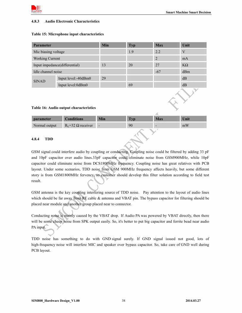
Smart Machine Smart Decision
SIM808_Hardware Design_V1.00 2014.03.27 38
4.8.3 Audio Electronic Characteristics
Table 15: Microphone input characteristics
Parameter Min Typ Max Unit
Mic biasing voltage 1.9 2.2 V
Working Current 2 mA
Input impedance(differential) 13 20 27 KΩ
Idle channel noise -67 dBm
Input level:-40dBm0 29 dB SINAD
Input level:0dBm0 69 dB
Table 16: Audio output characteristics
parameter Conditions Min Typ Max Unit
Normal output RL=32 Ω receiver - 90 - mW
4.8.4 TDD
GSM signal could interfere audio by coupling or conducting. Coupling noise could be filtered by adding 33 pF and 10pF capacitor over audio lines.33pF capacitor could eliminate noise from GSM900MHz, while 10pF capacitor could eliminate noise from DCS1800MHz frequency. Coupling noise has great relatives with PCB layout. Under some scenarios, TDD noise from GSM 900MHz frequency affects heavily, but some different story is from GSM1800MHz fervency, so customer should develop this filter solution according to field test result. GSM antenna is the key coupling interfering source of TDD noise. Pay attention to the layout of audio lines which should be far away from RF cable & antenna and VBAT pin. The bypass capacitor for filtering should be placed near module and another group placed near to connector. Conducting noise is mainly caused by the VBAT drop. If Audio PA was powered by VBAT directly, then there will be some cheep noise from SPK output easily. So, it's better to put big capacitor and ferrite bead near audio PA input. TDD noise has something to do with GND signal surely. If GND signal issued not good, lots of high-frequency noise will interfere MIC and speaker over bypass capacitor. So, take care of GND well during PCB layout.

Smart Machine Smart Decision
4.9 Bluetooth
SIM808 supports Bluetooth function, customer only needs to design the Bluetooth antenna, and then customer can operate Bluetooth conveniently by AT commands. For the detail commands about Bluetooth please refer to document [1]
Fully compliant with Bluetooth specification3.0 + EDR Support operation with GPS and GSM/GPRS worldwide radio systems Fully integrated PA provides 10dbm output power Up to 4 simultaneous active ACL links Support sniff mode
Support PCM interface and built-in programmable transcoders for liner voice with transmission.
4.9.1 Bluetooth Antenna Interface
The module provides a Bluetooth antenna interface named ANT_BT. External antenna must be matched properly to achieve best performance, so the matching circuit is necessary, the connection is recommended as the following figure:
Figure 35: Bluetooth antenna matching circuit R201, C201, C202 are the matching circuit, the values depend on antenna debug result. Normally R201 is 0Ω, C201 and C202 are not mounted.
4.10 SIM Card Interface
The SIM interface complies with the GSM Phase 1 specification and the new GSM Phase 2+ specification for FAST 64 kbps SIM card. Both 1.8V and 3.0V SIM card are supported. The SIM interface is powered from an internal regulator in the module.
SIM808_Hardware Design_V1.00 2014.03.27 39
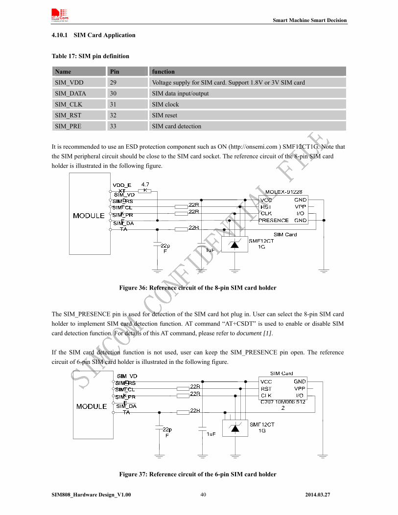
Smart Machine Smart Decision
4.10.1 SIM Card Application
Table 17: SIM pin definition
Name Pin function
SIM_VDD 29 Voltage supply for SIM card. Support 1.8V or 3V SIM card
SIM_DATA 30 SIM data input/output
SIM_CLK 31 SIM clock
SIM_RST 32 SIM reset
SIM_PRE 33 SIM card detection
It is recommended to use an ESD protection component such as ON (http://onsemi.com ) SMF12CT1G. Note that the SIM peripheral circuit should be close to the SIM card socket. The reference circuit of the 8-pin SIM card holder is illustrated in the following figure.
Figure 36: Reference circuit of the 8-pin SIM card holder
The SIM_PRESENCE pin is used for detection of the SIM card hot plug in. User can select the 8-pin SIM card holder to implement SIM card detection function. AT command “AT+CSDT” is used to enable or disable SIM card detection function. For details of this AT command, please refer to document [1].
If the SIM card detection function is not used, user can keep the SIM_PRESENCE pin open. The reference circuit of 6-pin SIM card holder is illustrated in the following figure.
Figure 37: Reference circuit of the 6-pin SIM card holder
SIM808_Hardware Design_V1.00 2014.03.27 40
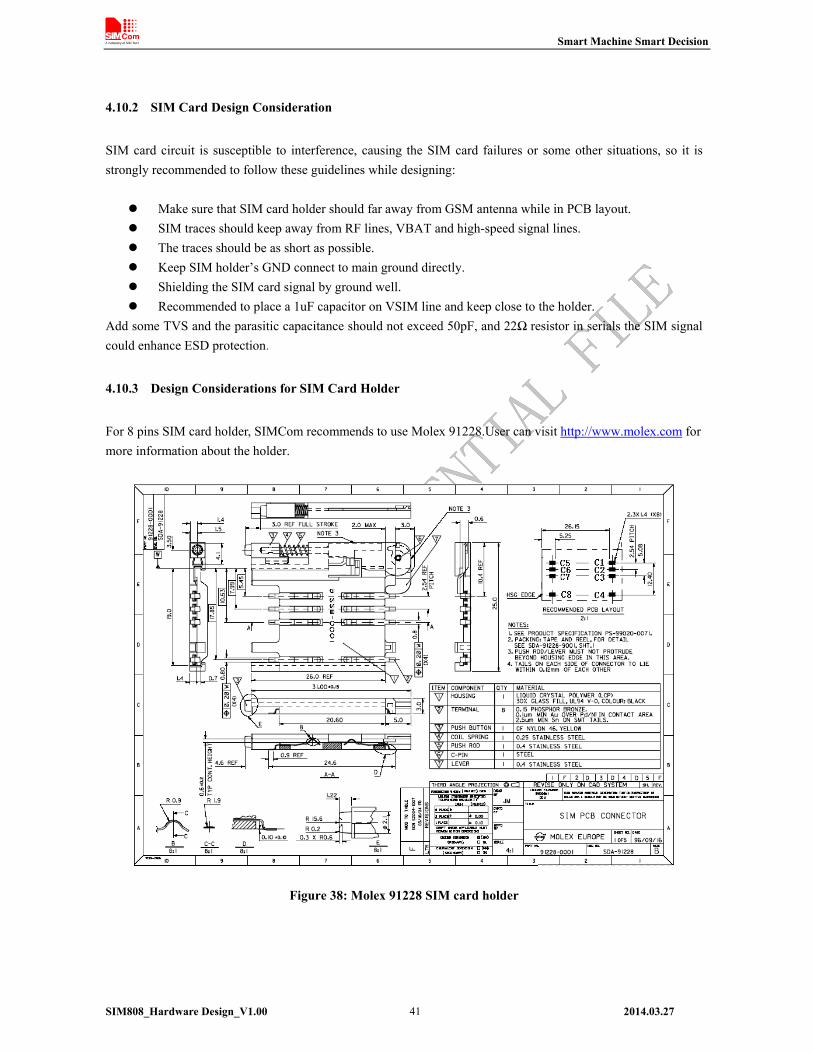
Smart Machine Smart Decision
4.10.2 SIM Card Design Consideration
SIM card circuit is susceptible to interference, causing the SIM card failures or some other situations, so it is strongly recommended to follow these guidelines while designing:
Make sure that SIM card holder should far away from GSM antenna while in PCB layout. SIM traces should keep away from RF lines, VBAT and high-speed signal lines. The traces should be as short as possible. Keep SIM holder’s GND connect to main ground directly. Shielding the SIM card signal by ground well. Recommended to place a 1uF capacitor on VSIM line and keep close to the holder.
Add some TVS and the parasitic capacitance should not exceed 50pF, and 22Ω resistor in serials the SIM signal could enhance ESD protection.
4.10.3 Design Considerations for SIM Card Holder
For 8 pins SIM card holder, SIMCom recommends to use Molex 91228.User can visit http://www.molex.com for more information about the holder.
Figure 38: Molex 91228 SIM card holder
SIM808_Hardware Design_V1.00 2014.03.27 41

Smart Machine Smart Decision
Table 18: Pin description (Molex SIM card holder)
Pin name Signal Description
C1 SIM_VDD SIM card power supply
C2 SIM_RST SIM card reset
C3 SIM_CLK SIM card clock
C3 GND Connect to GND
C5 GND Connect to GND
C6 VPP Not connect
C7 SIM_DATA SIM card data I/O
C8 SIM_PRE Detect SIM card presence
For 6-pin SIM card holder, SIMCom recommends to use Amphenol C707 10M006 5122 .User can visit http://www.amphenol.com for more information about the holder.
Figure 39: Amphenol C707 10M006 5122 SIM card holder
Table 19: Pin description (Amphenol SIM card holder)
SIM808_Hardware Design_V1.00 2014.03.27 42
Pin name Signal Description
C1 VSIM SIM card power supply
C2 SIM_RST SIM card reset
C3 SIM_CLK SIM card clock
C5 GND Connect to GND
C6 VPP Not connect
C7 SIM_DATA SIM card data I/O

Smart Machine Smart Decision
4.11 PCM Interface
SIM808 provides PCM interface.
Table 20: PCM pin definition
Pin name Pin number Description
PCM_OUT 48 PCM data output
PCM_IN 47 PCM data input
PCM_SYNC 45 PCM synchrony
PCM_CLK 46 PCM clock
SIM808 PCM interface only supports master mode, data length is 16 bits (linear), and PCM clock rate is 256 KHz. Table 21: PCM pin specification
Feature specification
Line Interface Format Linear(Fixed)
Data length 16bits(Fixed)
PCM Clock/Sync Source Master Mode(Fixed)
PCM Clock Rate 256Khz(Fixed)
PCM Sync Format Short sync/Long sync both support
Zero Padding/Sign extension
Default Zero Padding
Data Ordering MSB/LSB both support
Note: User can use AT command control PCM interface, for details please refer to document [1].
4.11.1 PCM Multiplex Function
With GPIO5 and GPIO6, PCM interface can be configured as SPI or SD interface, the following table shows the detailed multiplex function. Table 22: PCM Multiplex Function
Name Pin number Mode 0(default) Mode 1 Mode 2 Mode 3
PCM_OUT 48 PCM_OUT GPIO10 MC3DA3 /
PCM_IN 47 PCM_IN DISP_DATA MC3DA2 GPIO9
PCM_SYNC 45 PCM_SYNC DISP_CS MC3CK GPIO7
PCM_CLK 46 PCM_CLK GPIO8 MC3CM0 GPIO8
GPIO6 44 GPIO6 DISP_CLK MC3DA1 /
GPIO5 43 GPIO5 DISP_D/C MC3DA0 /
Note: Multiplex Function need different software version.
SIM808_Hardware Design_V1.00 2014.03.27 43

Smart Machine Smart Decision
4.11.2 PCM Interface
Refer to the following figure for PCM design:
Figure 40: PCM reference circuit
4.11.3 LCD Display/SPI Interface
SIM808 provides a serial interface. It could be used as SPI interface in the embedded AT application. For details about embedded AT application, please refer to document [1].
Refer to the following figure for SPI design:
DISP_D/C
DISP_CS
SPI_D/C
SPI_CS
SPI_CLKDISP_CLK
SPI_DATADISP_DATA
GND GND
Figure 41: LCD reference circuit
Note: This function is not supported in the standard firmware. If user wants this function, the firmware must be customized.
Please contact SIMCom for more details.
SIM808_Hardware Design_V1.00 2014.03.27 44
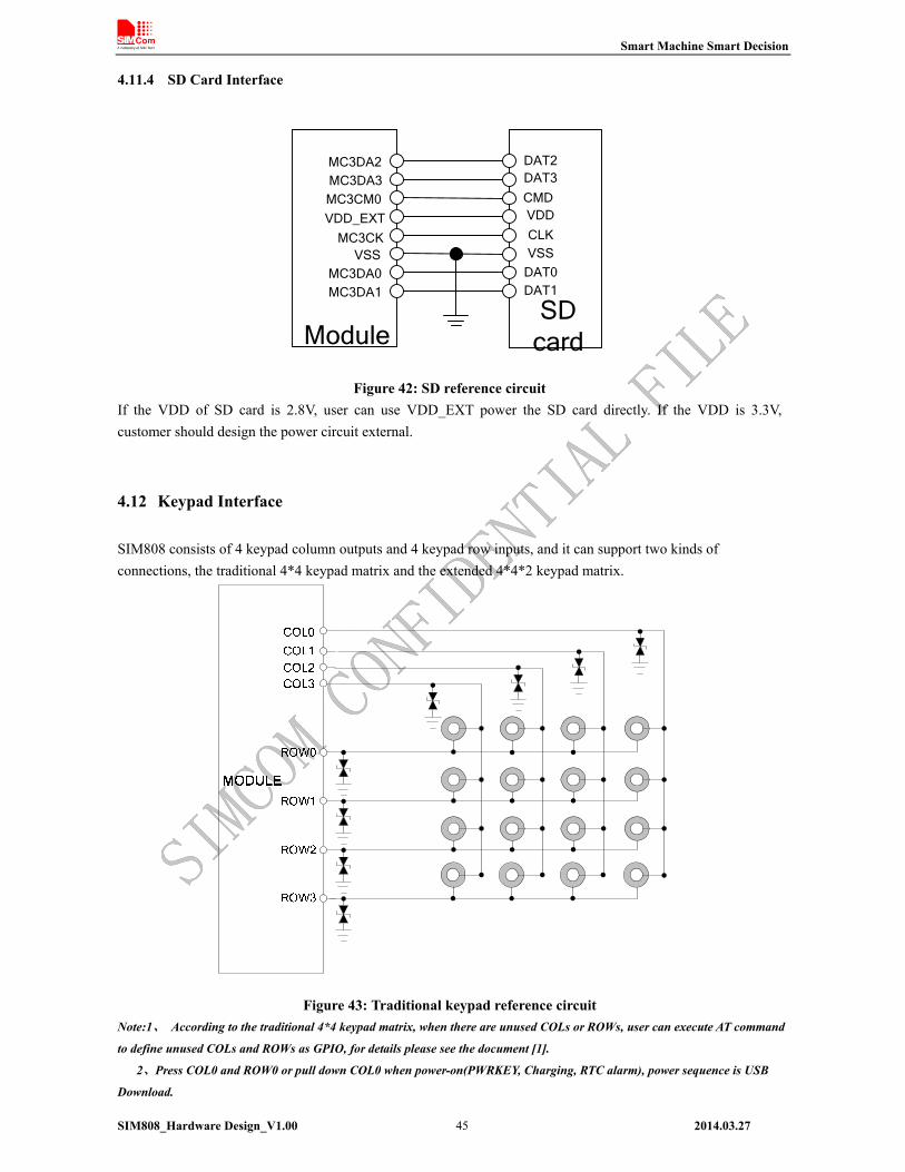
Smart Machine Smart Decision
4.11.4 SD Card Interface
Module
DAT2DAT3
CMDVDD
CLKVSS
DAT0DAT1
MC3DA2MC3DA3
MC3CM0
VDD_EXT
MC3CKVSS
MC3DA0
MC3DA1
SD card
Figure 42: SD reference circuit
If the VDD of SD card is 2.8V, user can use VDD_EXT power the SD card directly. If the VDD is 3.3V, customer should design the power circuit external.
4.12 Keypad Interface
SIM808 consists of 4 keypad column outputs and 4 keypad row inputs, and it can support two kinds of connections, the traditional 4*4 keypad matrix and the extended 4*4*2 keypad matrix.
Figure 43: Traditional keypad reference circuit
Note:1、 According to the traditional 4*4 keypad matrix, when there are unused COLs or ROWs, user can execute AT command
to define unused COLs and ROWs as GPIO, for details please see the document [1].
2、Press COL0 and ROW0 or pull down COL0 when power-on(PWRKEY, Charging, RTC alarm), power sequence is USB
Download.
SIM808_Hardware Design_V1.00 2014.03.27 45
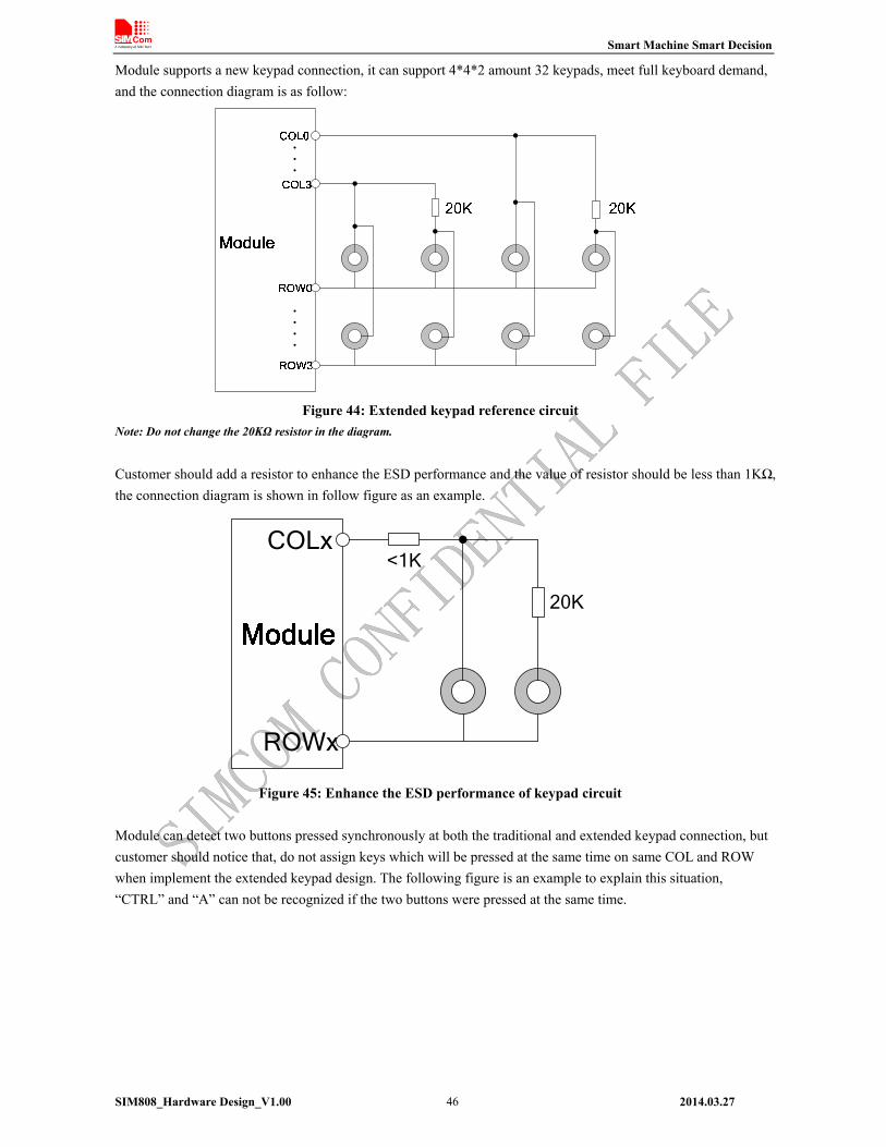
Smart Machine Smart Decision
Module supports a new keypad connection, it can support 4*4*2 amount 32 keypads, meet full keyboard demand, and the connection diagram is as follow:
Figure 44: Extended keypad reference circuit
Note: Do not change the 20KΩ resistor in the diagram. Customer should add a resistor to enhance the ESD performance and the value of resistor should be less than 1KΩ, the connection diagram is shown in follow figure as an example.
ROWx
COLx<1K
20K
Figure 45: Enhance the ESD performance of keypad circuit Module can detect two buttons pressed synchronously at both the traditional and extended keypad connection, but customer should notice that, do not assign keys which will be pressed at the same time on same COL and ROW when implement the extended keypad design. The following figure is an example to explain this situation, “CTRL” and “A” can not be recognized if the two buttons were pressed at the same time.
SIM808_Hardware Design_V1.00 2014.03.27 46

Smart Machine Smart Decision
Figure 46: Keypad detected
Table 23: Pin definition of the keypad interface
Name Pin Function Default state
COL0 62 Pull up
COL1 61 Pull down
COL2 60 Pull down
COL3 59
Keypad matrix column
Pull down
ROW0 58 Pull down
ROW1 57 Pull down
ROW2 56 Pull down
ROW3 55
Keypad matrix row
Pull down
Table 24: Keypad multiplex function
Pin name Pin number Mode 0(default) Mode 1
COL0 62 COL0 GPIO18
COL1 61 COL1 GPIO17
COL2 60 COL2 GPIO16
COL3 59 COL3 GPIO15
ROW0 58 ROW0 GPIO14
ROW1 57 ROW1 GPIO13
ROW2 56 ROW2 GPIO12
ROW3 55 ROW3 GPIO11
Note: Multiplex Function need different software version .
4.13 I2C BUS
The SIM808 provides an I2C interface, it can be driven by either the master or slave and conform to the I2C specification. It has the following features:
Compliant master mode operation
SIM808_Hardware Design_V1.00 2014.03.27 47
Smart Machine Smart Decision
Adjustable clock speed for LS/FS mode operation Support 7-bit/10-bit addressing Support high speed mode Support slave clock extension START/STOP/REPEATED condition Manual transfer mode Multi-write per transfer (up to 8 data bytes for non-DMA mode) Multi-read per transfer (up to 8 data bytes for non-DMA mode) Multi-transfer per transaction Combined format transfer with length change capability
Active drive/write-and I/O configuration Table 25: Pin definition of the I2C
Pin name Pin number Description
SCL 39 I2C serial bus clock
SDA 38 I2C serial bus data
SIM808_Hardware Design_V1.00 2014.03.27 48
Note: I2C has been pulled up to 2.8V via 4.7KΩ.
Table 26: I2C multiplex function
Pin name Pin number Mode 0(default) Mode 1
SCL 39 SCL GPIO2
SDA 38 SDA GPIO1
4.13.1 General Purpose Input/Output (GPIO)
SIM808 provides 2 GPIO pins. The output voltage level of the GPIO can be set by the AT command “AT+ SGPIO”. The input voltage level of the GPIO can also be read by the AT command “AT+ SGPIO”. For more details, please refer to document [1].
Table 27: Pin definition of the GPIO
Pin name Pin number Reset state
GPIO6 44 Pull down
GPIO5 43 Pull down
4.14 ADC
Table 28: Pin definition of the ADC Pin name Pin number Description
ADC1 23 Analog to Digital Converter
ADC2 24 Analog to Digital Converter
SIM808 provides two auxiliary ADC, which can be used to measure the voltage. User can use AT command
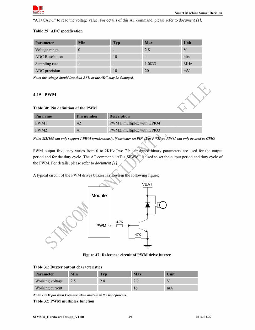
Smart Machine Smart Decision
“AT+CADC” to read the voltage value. For details of this AT command, please refer to document [1].
Table 29: ADC specification
Parameter Min Typ Max Unit
Voltage range 0 - 2.8 V
ADC Resolution - 10 - bits
Sampling rate - - 1.0833 MHz
ADC precision 10 20 mV
Note: the voltage should less than 2.8V, or the ADC may be damaged.
4.15 PWM
Table 30: Pin definition of the PWM
Pin name Pin number Description
PWM1 42 PWM1, multiplex with GPIO4
PWM2 41 PWM2, multiplex with GPIO3
Note: SIM808 can only support 1 PWM synchronously, if customer set PIN 42 as PWM, so PIN41 can only be used as GPIO.
PWM output frequency varies from 0 to 2KHz.Two 7-bit unsigned binary parameters are used for the output period and for the duty cycle. The AT command “AT + SPWM” is used to set the output period and duty cycle of the PWM. For details, please refer to document [1]. A typical circuit of the PWM drives buzzer is shown in the following figure:
4.7K
47K
VBAT
PWM
Figure 47: Reference circuit of PWM drive buzzer
Table 31: Buzzer output characteristics
Parameter Min Typ Max Unit
Working voltage 2.5 2.8 2.9 V
Working current 16 mA
Note: PWM pin must keep low when module in the boot process.
Table 32: PWM multiplex function
SIM808_Hardware Design_V1.00 2014.03.27 49
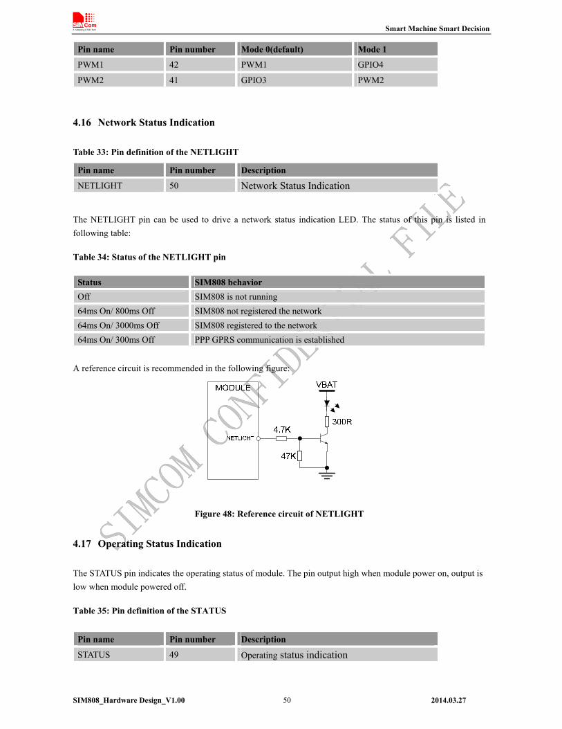
Smart Machine Smart Decision
Pin name Pin number Mode 0(default) Mode 1
PWM1 42 PWM1 GPIO4
PWM2 41 GPIO3 PWM2
SIM808_Hardware Design_V1.00 2014.03.27 50
4.16 Network Status Indication
Table 33: Pin definition of the NETLIGHT Pin name Pin number Description
NETLIGHT 50 Network Status Indication
The NETLIGHT pin can be used to drive a network status indication LED. The status of this pin is listed in following table:
Table 34: Status of the NETLIGHT pin
Status SIM808 behavior Off SIM808 is not running 64ms On/ 800ms Off SIM808 not registered the network 64ms On/ 3000ms Off SIM808 registered to the network 64ms On/ 300ms Off PPP GPRS communication is established
A reference circuit is recommended in the following figure:
Figure 48: Reference circuit of NETLIGHT
4.17 Operating Status Indication
The STATUS pin indicates the operating status of module. The pin output high when module power on, output is low when module powered off.
Table 35: Pin definition of the STATUS
Pin name Pin number Description
STATUS 49 Operating status indication
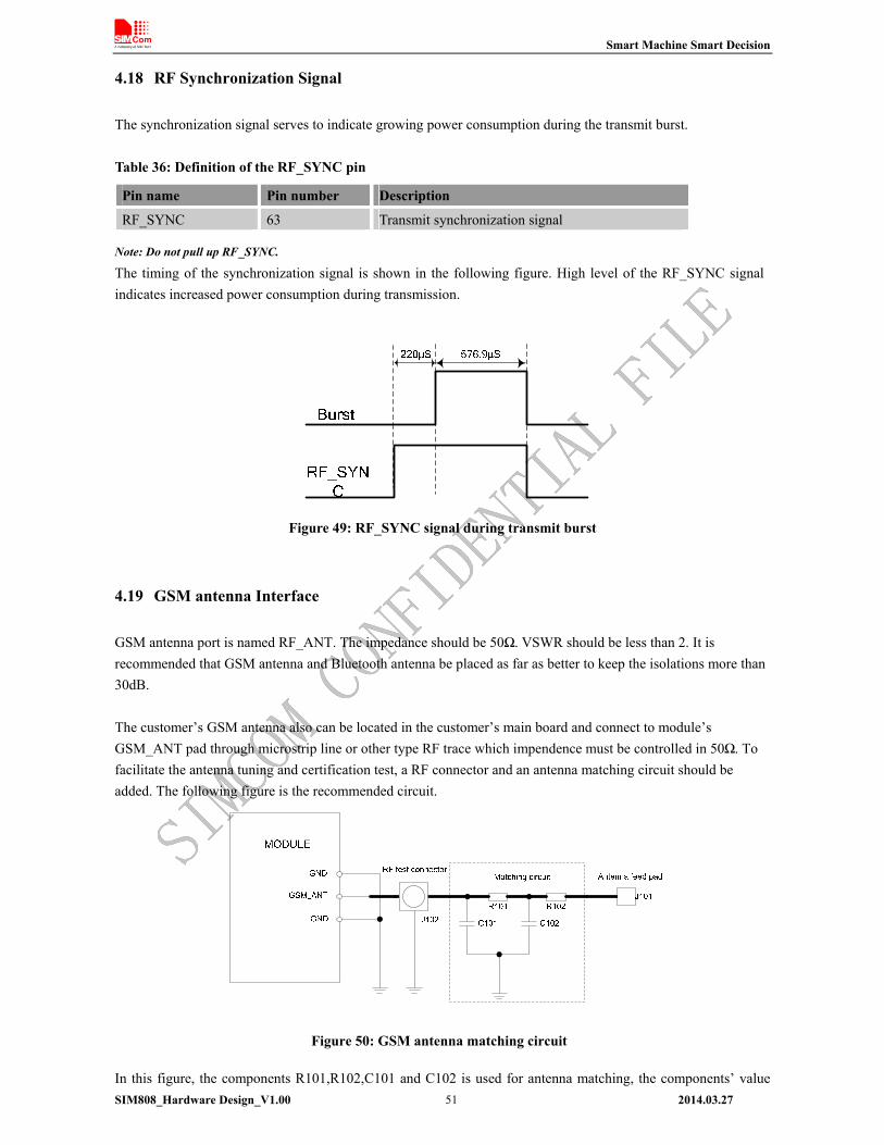
Smart Machine Smart Decision
4.18 RF Synchronization Signal
The synchronization signal serves to indicate growing power consumption during the transmit burst. Table 36: Definition of the RF_SYNC pin
Pin name Pin number Description
RF_SYNC 63 Transmit synchronization signal
Note: Do not pull up RF_SYNC. The timing of the synchronization signal is shown in the following figure. High level of the RF_SYNC signal indicates increased power consumption during transmission.
Figure 49: RF_SYNC signal during transmit burst
4.19 GSM antenna Interface
GSM antenna port is named RF_ANT. The impedance should be 50Ω. VSWR should be less than 2. It is recommended that GSM antenna and Bluetooth antenna be placed as far as better to keep the isolations more than 30dB.
The customer’s GSM antenna also can be located in the customer’s main board and connect to module’s GSM_ANT pad through microstrip line or other type RF trace which impendence must be controlled in 50Ω. To facilitate the antenna tuning and certification test, a RF connector and an antenna matching circuit should be added. The following figure is the recommended circuit.
Figure 50: GSM antenna matching circuit
In this figure, the components R101,R102,C101 and C102 is used for antenna matching, the components’ value SIM808_Hardware Design_V1.00 2014.03.27 51
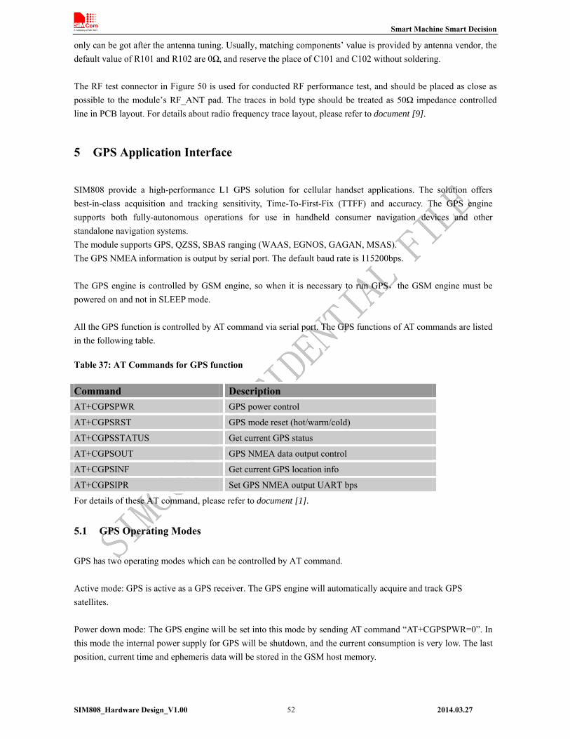
Smart Machine Smart Decision
SIM808_Hardware Design_V1.00 2014.03.27 52
only can be got after the antenna tuning. Usually, matching components’ value is provided by antenna vendor, the default value of R101 and R102 are 0Ω, and reserve the place of C101 and C102 without soldering. The RF test connector in Figure 50 is used for conducted RF performance test, and should be placed as close as possible to the module’s RF_ANT pad. The traces in bold type should be treated as 50Ω impedance controlled line in PCB layout. For details about radio frequency trace layout, please refer to document [9].
5 GPS Application Interface
SIM808 provide a high-performance L1 GPS solution for cellular handset applications. The solution offers best-in-class acquisition and tracking sensitivity, Time-To-First-Fix (TTFF) and accuracy. The GPS engine supports both fully-autonomous operations for use in handheld consumer navigation devices and other standalone navigation systems. The module supports GPS, QZSS, SBAS ranging (WAAS, EGNOS, GAGAN, MSAS). The GPS NMEA information is output by serial port. The default baud rate is 115200bps. The GPS engine is controlled by GSM engine, so when it is necessary to run GPS,the GSM engine must be powered on and not in SLEEP mode. All the GPS function is controlled by AT command via serial port. The GPS functions of AT commands are listed in the following table.
Table 37: AT Commands for GPS function
Command Description AT+CGPSPWR GPS power control
AT+CGPSRST GPS mode reset (hot/warm/cold)
AT+CGPSSTATUS Get current GPS status
AT+CGPSOUT GPS NMEA data output control
AT+CGPSINF Get current GPS location info
AT+CGPSIPR Set GPS NMEA output UART bps
For details of these AT command, please refer to document [1].
5.1 GPS Operating Modes
GPS has two operating modes which can be controlled by AT command. Active mode: GPS is active as a GPS receiver. The GPS engine will automatically acquire and track GPS satellites. Power down mode: The GPS engine will be set into this mode by sending AT command “AT+CGPSPWR=0”. In this mode the internal power supply for GPS will be shutdown, and the current consumption is very low. The last position, current time and ephemeris data will be stored in the GSM host memory.

Smart Machine Smart Decision
5.2 GPS Power on/down Scenarios
5.2.1 Power on GPS engine
User can power on GPS engine by sending AT command “AT+CGPSPWR=1”.
5.2.2 Power down GPS engine
User can power down GPS engine by sending AT command “AT+CGPSPWR=0”.
5.3 GPS Antenna Interface
5.3.1 GPS Antenna Interface
The customer’s GPS antenna also can be located in the customer’s main board and connect to module’s GPS_ANT pad through microstrip line or other type RF trace which impendence must be 50Ω.
Figure 51: GPS antenna matching circuit
In Figure 51, the components R101, C101 and C102 is used for antenna matching, the components’ value only can be got after the antenna tuning. Usually, matching components’ value is provided by antenna vendor, the default value of R101 is 0Ω, and users need to reserve the place of C101 and C102 without soldering. The traces in bold type should be treated as 50Ω impedance controlled line in PCB layout.
5.3.2 GPS Antenna Choice Consideration
To obtain excellent GPS reception performance, a good antenna will always be required. The antenna is the most critical item for successful GPS reception in a weak signal environment. Proper choice and placement of the antenna will ensure that satellites at all elevations can be seen, and therefore, accurate fix measurements are obtained. Most customers contract with antenna design houses to properly measure the radiation pattern of the final mounted configuration in a plastic housing with associated components near the antenna. Linear antennas are becoming more popular, and the gain is reasonable, since a smaller ground plane can be used. User can consider following factors as:
Choose a linear antenna with a reasonably uniform hemispherical gain pattern of >-4dBi.
Use of an antenna with lower gain then this will give less than desirable results. Please note that a RHCP
antenna with a gain of 3dBi, equates to a linear polarized antenna of 0dBi. SIM808_Hardware Design_V1.00 2014.03.27 53

Smart Machine Smart Decision
SIM808_Hardware Design_V1.00 2014.03.27 54
Proper ground plane sizing is a critical consideration for small GPS antennas.
Proper placement of the GPS antenna should always be the FIRST consideration in integrating the SIM808
GPS Module.
If the customer’s design will allow for a ceramic RHCP patch antenna with an appropriately sized ground plane, and the patch is normally oriented towards the sky, then that particular solution usually works the best. Note that if the patch antenna ground plane is less than 60x60mm, then compromises to the beam width and gain pattern could result. Usually the gain becomes very directional, and looses several dB of performance. Since results can vary, measuring the antenna radiation pattern in the final housing in an appropriate anechoic chamber is required. Some customers do not have the size availability to implement a patch antenna approach. In that instance, use of a Linear Polarized (LP) antenna is the next best alternative. There are new ceramic LP antennas on the market that exhibit reasonable gain characteristics once properly mounted in the housing, and when matched to an appropriate sized ground. Generally the ground plane requirements are smaller for a LP antenna when compared to a patch, but once again, proper testing in an anechoic chamber is a mandatory requirement. These ceramic elements will need to be located near the end of the ground plane, and will require several millimeters of clearance between the closest component. It is important to note that use of a LP antenna will result in a minimum of 3dB of gain loss when compared to a RHCP antenna at a defined elevation. This is due to the right hand gain rule of antenna propagation. Use of PIFA antenna is another LP possibility, but the PIFA usually exhibits a considerable amount of gain nulls, or “holes” in the radiation pattern. This will be undesirable for obtaining a low circular error probability (CEP), since the antenna may not allow the receiver to capture the desired satellite at the ideal orientation due to these noted gain nulls. Once again, careful testing in an appropriate anechoic chamber is required. If the customer’s design is for automotive applications, then an active antenna can be used and located on top of the car in order to achieve the best signal quality. GPS antenna choice should be based on the designing product and other conditions. For detailed Antenna designing consideration, please refer to related antenna vendor’s design recommendation. The antenna vendor will offer further technical support and tune their antenna characteristic to achieve successful GPS reception performance depending on the customer’s design.
6 Electrical, Reliability and Radio Characteristics
6.1 Absolute Maximum Ratings
The absolute maximum ratings stated in following table are stress ratings under non-operating conditions. Stresses beyond any of these limits will cause permanent damage to SIM808.
Table 38: Absolute maximum ratings
Symbol Min Typ Max Unit

Smart Machine Smart Decision
SIM808_Hardware Design_V1.00 2014.03.27 55
VBAT - - 4.5 V
Peak Current 0 - 2.0 A
VBUS - - 30 V
II* - - 8 mA
IO* - - 8 mA
* These parameters are for digital interface pins, such as keypad, GPIO, I2C, UART, LCD and PCM..
6.2 Recommended Operating Conditions
Table 39: Recommended operating conditions
Symbol Parameter Min Typ Max Unit
VBAT Power supply voltage 3.4 4.0 4.4 V
TOPER Operating temperature -40 +25 +85
TSTG Storage temperature -45 +90
6.3 Digital Interface Characteristics
Table 40: Digital interface characteristics
Symbol Parameter Min Typ Max Unit
IIH High-level input current -10 - 10 uA
IIL Low-level input current -10 - 10 uA
VIH High-level input voltage 2.4 - - V
VIL Low-level input voltage - - 0.4 V
VOH High-level output voltage 2.7 - - V
VOL Low-level output voltage - - 0.1 V
* These parameters are for digital interface pins, such as keypad, GPIO, I2C, UART, LCD, PWMs and DEBUG.
6.4 SIM Card Interface Characteristics
Table 41: SIM card interface characteristics
Symbol Parameter Min Typ Max Unit
IIH High-level input current -1 - 1 uA
IIL Low-level input current -1 - 1 uA
1.4 - - V VIH High-level input voltage
2.4 - - V
- - 0.27 V VIL Low-level input voltage
0.4 V
1.62 - - V VOH High-level output voltage
2.7 - - V

Smart Machine Smart Decision
SIM808_Hardware Design_V1.00 2014.03.27 56
- - 0.36 V VOL Low-level output voltage
- - 0.4 V
6.5 SIM_VDD Characteristics
Table 42: SIM_VDD characteristics Symbol Parameter Min Typ Max Unit
- 3 - VO
Output voltage
- 1.80 - V
IO Output voltage - - 10 mA
6.6 VDD_EXT Characteristics
Table 43: VDD_EXT characteristics
Symbol Parameter Min Typ Max Unit
VO Output voltage 2.70 2.80 2.95 V
IO Output current - - 50 mA
6.7 VRTC Characteristics
Table 44: VRTC characteristics
Symbol Parameter Min Typ Max Unit
VRTC-IN VRTC input voltage - 2.8 - V
IRTC-IN VRTC input current - 3 - uA
VRTC-OUT VRTC output voltage - 2.8 - V
IRTC-OUT VRTC output current - 2 uA
6.8 Current Consumption (VBAT = 4V, GPS engine is powered down)
Table 45: GSM current consumption*
Symbol Parameter Conditions Min Typ Max Unit
Voltage 3.4 4.0 4.4 V
Power drop PCL=5 350 mV
VBAT
Voltage ripple PCL=5 @ f<200kHz @ f>200kHz
50 2
mV mV

Smart Machine Smart Decision
SIM808_Hardware Design_V1.00 2014.03.27 57
Power down mode 38 50 uA
Sleep mode (AT+CFUN=1): ( BS-PA-MFRMS=9 ) ( BS-PA-MFRMS=5) ( BS-PA-MFRMS=2)
1.965 1.7 1.4
mA mA mA
Idle mode (AT+CFUN=1): EGSM900
22.1
mA
Voice call (PCL=5): GSM850 EGSM900 DCS1800 PCS1900
207.63 202.32 139.825 137.805
mA mA
Data mode GPRS (1Rx,4Tx): GSM850 EGSM900 DCS1800 PCS1900
445.82 424.32 293.62 279.18
mA mA
Data mode GPRS (3Rx,2Tx): GSM850 EGSM900 DCS1800 PCS1900
329.79 220.62 223.18 218.34
mA mA
IVBAT Average current
Data mode GPRS (4Rx,1Tx): GSM850 EGSM900 DCS1800 PCS1900
221.25 220.62 158.01 158.62
mA mA
IMAX Peak current During TX burst 2.0 A
* In above table the current consumption value is the typical one of the module tested in laboratory. In the mass production stage,
there may be differences among each individual.
6.9 Electro-Static Discharge
SIM808 is an ESD sensitive component, so more attention should be paid to the procedure of handling and packaging. The ESD test results are shown in the following table.
Table 46: The ESD characteristics (Temperature: 25, Humidity: 45 %)
Pin Contact discharge Air discharge
VBAT ±5KV ±10KV
GND ±5KV ±10KV
RXD, TXD ±4KV ±8KV
Antenna port ±5KV ±10KV

Smart Machine Smart Decision
SIM808_Hardware Design_V1.00 2014.03.27 58
SPK1P/ SPK1N MIC1P/ MIC1N
±4KV ±8KV
PWRKEY ±4KV ±8KV
Note: It is suggested that customers in serials with 100ohm resistances on UART lines for ESD consideration.
6.10 Radio Characteristics
6.10.1 Module RF Output Power
The following table shows the module conducted output power, it is followed by the 3GPP TS 05.05 technical specification requirement.
Table 47: SIM808 GSM 900 and GSM 850 conducted RF output power
GSM 900 and EGSM 850
Tolerance (dB) for conditions PCL Nominal output power (dBm)
Normal Extreme
0-2 39 ±2 ±2.5
3 37 ±3 ±4
4 35 ±3 ±4
5 33 ±3 ±4
6 31 ±3 ±4
7 29 ±3 ±4
8 27 ±3 ±4
9 25 ±3 ±4
10 23 ±3 ±4
11 21 ±3 ±4
12 19 ±3 ±4
13 17 ±3 ±4
14 15 ±3 ±4
15 13 ±3 ±4
16 11 ±5 ±6
17 9 ±5 ±6
18 7 ±5 ±6
19-31 5 ±5 ±6
Table 48: SIM808 DCS 1800 and PCS 1900 conducted RF output power
DCS 1800 and PCS 1900
Tolerance (dB) for conditions PCL Nominal output power (dBm)
Normal Extreme

Smart Machine Smart Decision
SIM808_Hardware Design_V1.00 2014.03.27 59
29 36 ±2 ±2.5
30 34 ±3 ±4
31 32 ±3 ±4
0 30 ±3 ±4
1 28 ±3 ±4
2 26 ±3 ±4
3 24 ±3 ±4
4 22 ±3 ±4
5 20 ±3 ±4
6 18 ±3 ±4
7 16 ±3 ±4
8 14 ±3 ±4
9 12 ±4 ±5
10 10 ±4 ±5
11 8 ±4 ±5
12 6 ±4 ±5
13 4 ±4 ±5
14 2 ±5 ±6
15-28 0 ±5 ±6
For the module’s output power, the following should be noted: At GSM900 and GSM850 band, the module is a class 4 device, so the module’s output power should not exceed 33dBm, and at the maximum power level, the output power tolerance should not exceed +/-2dB under normal condition and +/-2.5dB under extreme condition. At DCS1800 and PCS1900 band, the module is a class 1 device, so the module’s output power should not exceed 30dBm, and at the maximum power level, the output power tolerance should not exceed +/-2dB under normal condition and +/-2.5dB under extreme condition.
6.10.2 Module RF Receive Sensitivity
The following table shows the module’s conducted receive sensitivity, it is tested under static condition.
Table 49: SIM808 conducted RF receive sensitivity
Frequency Receive sensitivity(Typical) Receive sensitivity(Max)
GSM850 -109dBm -107dBm
EGSM900 -109dBm -107dBm
DCS1800 -109dBm -107dBm
PCS1900 -109dBm -107dBm

Smart Machine Smart Decision
SIM808_Hardware Design_V1.00 2014.03.27 60
6.10.3 Module Operating Frequencies
The following table shows the module’s operating frequency range; it is followed by the 3GPP TS 05.05 technical specification requirement.
Table 50: SIM808 operating frequencies
Frequency Receive Transmit
GSM850 869 ~ 894MHz 824 ~ 849 MHz
EGSM900 925 ~ 960MHz 880 ~ 915MHz
DCS1800 1805 ~ 1880MHz 1710 ~ 1785MHz
PCS1900 1930 ~ 1990MHz 1850 ~ 1910MHz
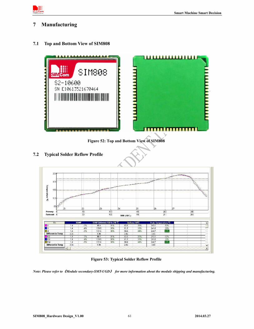
Smart Machine Smart Decision
7 Manufacturing
7.1 Top and Bottom View of SIM808
Figure 52: Top and Bottom View of SIM808
7.2 Typical Solder Reflow Profile
Figure 53: Typical Solder Reflow Profile
Note: Please refer to《Module secondary-SMT-UGD》 for more information about the module shipping and manufacturing.
SIM808_Hardware Design_V1.00 2014.03.27 61

Smart Machine Smart Decision
SIM808_Hardware Design_V1.00 2014.03.27 62
7.3 The Moisture Sensitivity Level
The moisture sensitivity level of SIM808 is 3. The module should be mounted within 168 hours after unpacking in the environmental conditions of temperature <30°C and relative humidity of <60% (RH). It is necessary to bake the module if the above conditions are not met:
Table 51: Moisture classification level and floor life
Level Floor Life (out of bag) at factory ambient≤30°C /60% RH or as stated
1 Unlimited at ≤30°C /85% RH
2 1 year
2a 4 weeks
3 168 hours
4 72 hours
5 48 hours
5a 24 hours
6 Mandatory bake before use. After bake, it must be reflowed within the time limit specified on the label.
NOTES:
1. If the vacuum package is not open for 6 months or longer than the packing date, baking is also recommended before re-flow
soldering.
2. For product handling, storage, processing, IPC / JEDEC J-STD-033 must be followed.
7.4 Baking Requirements
Because of its sensitivity to moisture absorption, SIM808 should be baked sufficiently before re-flow soldering. Otherwise SIM808 will be at the risk of permanent damage during re-flow soldering. SIM808 should be baked 192 hours at temperature 40°C +5°C /-0°C and <5% RH for low-temperature device containers, or 72 hours at temperature 80°C±5°C for high-temperature device containers. Care should be taken that the plastic tray is not heat resistant, SIM808 modules should be taken out for baking, and otherwise the tray may be damaged by high-temperature during baking.
Table 52: Baking requirements
Baking temperature Moisture Time
40°C±5°C <5% 192 hours
120°C±5°C <5% 4 hours
Smart Machine Smart Decision
SIM808_Hardware Design_V1.00 2014.03.27 63
Appendix
A. Related Documents
Table 53: Related documents
SN Document name Remark
[1] SIM800_AT Command Manual
SIM800 AT Command Manual
[2] AN_SIM900_TCPIP TCP/IP Applications User Manual
[3] SIM900_Multiplexer User Manual_Application Note
SIM808 Multiplexer User Manual Application Note
[4] AN_SIM900 Series_Update Tool_UGD
SIM808 Series Update Tool User Guide
[5] AN_SIM900_AUDIO Applications Note About SIM808 Audio
[6] AN_SIM900_Audio LINE-IN input
Applications Note About SIM808 LINE-IN Input
[7] SIM900_Embedded AT Application Note
SIM808 Embedded AT Application Note
[8] AN_Serial Port Application Note About Serial Port
[9] AN_SIM900-TE PCB Layout & Schematic for Reference
Application Note About SIM808-TE PCB Layout & Schematic
[10] Module secondary-SMT-UGD
Module secondary SMT User Guide
[11] ITU-T Draft new recommendation V.25ter:
Serial asynchronous automatic dialing and control
[12] GSM 07.07: Digital cellular telecommunications (Phase 2+); AT command set for GSM Mobile Equipment (ME)
[13] GSM 07.10: Support GSM 07.10 multiplexing protocol
[14] GSM 07.05: Digital cellular telecommunications (Phase 2+); Use of Data Terminal Equipment – Data Circuit terminating Equipment (DTE – DCE) interface for Short Message Service (SMS) and Cell Broadcast Service (CBS)
[15] GSM 11.14: Digital cellular telecommunications system (Phase 2+); Specification of the SIM Application Toolkit for the Subscriber Identity Module – Mobile Equipment (SIM – ME) interface
[16] GSM 11.11: Digital cellular telecommunications system (Phase 2+); Specification of the Subscriber Identity Module – Mobile Equipment (SIM – ME) interface
[17] GSM 03.38: Digital cellular telecommunications system (Phase 2+); Alphabets and language-specific information
[18] GSM 11.10 Digital cellular telecommunications system (Phase 2); Mobile Station (MS) conformance specification; Part 1: Conformance specification

Smart Machine Smart Decision
SIM808_Hardware Design_V1.00 2014.03.27 64
B. Terms and Abbreviations
Table 54: Terms and Abbreviations
Abbreviation Description
ADC Analog-to-Digital Converter
AMR Adaptive Multi-Rate
CS Coding Scheme
CSD Circuit Switched Data
CTS Clear to Send
CEP Circular Error Probable
DTE Data Terminal Equipment (typically computer, terminal, printer)
DTR Data Terminal Ready
DTX Discontinuous Transmission
EFR Enhanced Full Rate
EGSM Enhanced GSM
EGNOS European Geostationary Navigation Overlay Service
ESD Electrostatic Discharge
ETS European Telecommunication Standard
FR Full Rate
GPRS General Packet Radio Service
GSM Global Standard for Mobile Communications
GPS Global Positioning System
GAGAN The GPS Aided Geo Augmented Navigation
HR Half Rate
IMEI International Mobile Equipment Identity
Li-ion Lithium-Ion
MO Mobile Originated
MS Mobile Station (GSM engine), also referred to as TE
MT Mobile Terminated
MSAS Multi-Functional Satellite Augmentation System
NMEA National Marine Electronics Association
PAP Password Authentication Protocol
PBCCH Packet Broadcast Control Channel
PCB Printed Circuit Board
PCL Power Control Level
PCS Personal Communication System, also referred to as GSM 1900
PDU Protocol Data Unit
PPP Point-to-point protocol
QZSS Quasi-Zenith Satellites System
RF Radio Frequency
RMS Root Mean Square (value)
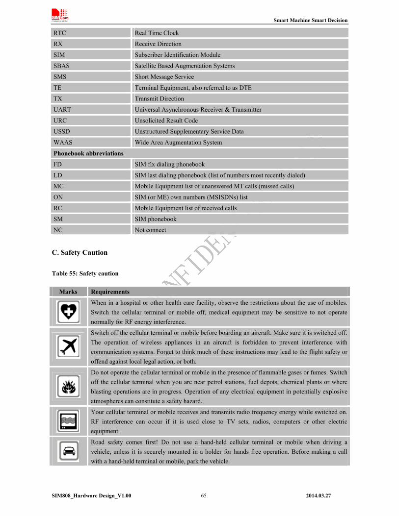
Smart Machine Smart Decision
RTC Real Time Clock
RX Receive Direction
SIM Subscriber Identification Module
SBAS Satellite Based Augmentation Systems
SMS Short Message Service
TE Terminal Equipment, also referred to as DTE
TX Transmit Direction
UART Universal Asynchronous Receiver & Transmitter
URC Unsolicited Result Code
USSD Unstructured Supplementary Service Data
WAAS Wide Area Augmentation System
Phonebook abbreviations
FD SIM fix dialing phonebook
LD SIM last dialing phonebook (list of numbers most recently dialed)
MC Mobile Equipment list of unanswered MT calls (missed calls)
ON SIM (or ME) own numbers (MSISDNs) list
RC Mobile Equipment list of received calls
SM SIM phonebook
NC Not connect
C. Safety Caution
Table 55: Safety caution
Marks Requirements
When in a hospital or other health care facility, observe the restrictions about the use of mobiles. Switch the cellular terminal or mobile off, medical equipment may be sensitive to not operate normally for RF energy interference.
Switch off the cellular terminal or mobile before boarding an aircraft. Make sure it is switched off. The operation of wireless appliances in an aircraft is forbidden to prevent interference with communication systems. Forget to think much of these instructions may lead to the flight safety or offend against local legal action, or both.
Do not operate the cellular terminal or mobile in the presence of flammable gases or fumes. Switch off the cellular terminal when you are near petrol stations, fuel depots, chemical plants or where blasting operations are in progress. Operation of any electrical equipment in potentially explosive atmospheres can constitute a safety hazard.
Your cellular terminal or mobile receives and transmits radio frequency energy while switched on. RF interference can occur if it is used close to TV sets, radios, computers or other electric equipment.
Road safety comes first! Do not use a hand-held cellular terminal or mobile when driving a vehicle, unless it is securely mounted in a holder for hands free operation. Before making a call with a hand-held terminal or mobile, park the vehicle.
SIM808_Hardware Design_V1.00 2014.03.27 65

Smart Machine Smart Decision
GSM cellular terminals or mobiles operate over radio frequency signals and cellular networks and cannot be guaranteed to connect in all conditions, for example no mobile fee or a invalid SIM card. While you are in this condition and need emergent help, please remember using emergency calls. In order to make or receive calls, the cellular terminal or mobile must be switched on and in a service area with adequate cellular signal strength. Some networks do not allow for emergency call if certain network services or phone features are in use (e.g. lock functions, fixed dialing etc.). You may have to deactivate those features before you can make an emergency call. Also, some networks require that a valid SIM card be properly inserted in the cellular terminal or mobile.
SIM808_Hardware Design_V1.00 2014.03.27 66
Uncontrolled Copy when printed or downloaded. Please refer to the 4D Systems website for the latest Revision of this document
2.4” microLCD PICASO Display uLCD-24PTU
Document Date: 22nd June 2015
Document Revision: 1.8 DATA
SH
EET

The uLCD-24PTU is a compact and cost effective Intelligent Display Module packed with plenty of features, ready to become the GUI for your target application. It is the perfect choice for many applications that require a front end smart graphics interface. Embedded at the heart of the design is the PICASO processor, which is driven by a highly optimised virtual core engine called EVE (Extensible Virtual Engine). An extensive range of hardware and software peripherals have been integrated into the design, to give the user freedom to adapt the module to suit almost any application. The display module is an elegant combination of a 2.4” (240x320) LCD Screen, audio amplifier and speaker, micro-SD card connector, Lithium Ion and Polymer battery support, along with a group of general purpose input/output pins (GPIO's), including I
2C and serial communications.
This module serves as a perfect solution to be deployed at the forefront of any product design, requiring a brilliance of colour, animation or images on any application. This PICASO driven Intelligent Display Module is a perfect example of where art meets technology.
The uLCD-24PTU has a 2.4’’ TFT LCD display at the forefront of the design that showcases the power and capabilities of the PICASO processor. Combining a resolution of 240x320 pixels with 65K True to Life colours, this module is perfect for animations, slideshows and other multimedia presentations.
Audio support provided on the display module is supplied by the PICASO processor, an on-board audio amplifier and 8Ω speaker. A simple instruction enables the user to play audio files while continuing the execution of the Users code, such as display updates, touch recognition, communications and much more.
The micro-SD card slot provides the user with expandable memory space suitable for multimedia file retrieval, including images, animations and movie clips, as well as data logging applications.
The module can be programmed in its native 4DGL language (similar to C), using the Workshop4 IDE software tool suite, or it can be configured as a serial slave device to use with your favourite host controller. The freedom is at your fingertips with this 2.4" intelligent microLCD module.
Overview
micro
LCD
PIC
ASO D
ISPLA
Y

Contents
1. Description ............................................................................................................................. 4
2. Features ................................................................................................................................. 4
3. Pin Configuration and Summary .............................................................................................. 5
4. Hardware Interface - Pins........................................................................................................ 7
Serial Ports - COM0, COM1 UARTS ........................................................................................................ 7 4.1.
General Purpose I/O ............................................................................................................................... 7 4.2.
System Pins ............................................................................................................................................ 8 4.3.
5. PmmC/Firmware Programming ............................................................................................... 9
6. Module Features .................................................................................................................... 9
Display – 2.4” TFT Touch Screen ............................................................................................................ 9 6.1.
PICASO Processor ................................................................................................................................... 9 6.2.
Audio .................................................................................................................................................... 10 6.3.
Lithium Batteries .................................................................................................................................. 10 6.4.
SD/SDHC Memory Cards ...................................................................................................................... 10 6.5.
FAT16 ................................................................................................................................................... 10 6.6.
7. Display Precautions .............................................................................................................. 11
8. Hardware Tools .................................................................................................................... 12
4D Programming Cable/Adaptor .......................................................................................................... 12 8.1.
Development Hardware ....................................................................................................................... 12 8.2.
9. 4DGL - Software Language .................................................................................................... 13
10. 4D Systems - Workshop 4 IDE .............................................................................................. 13
Workshop 4 – Designer Environment ................................................................................................ 14 10.1.
Workshop 4 – ViSi Environment ......................................................................................................... 14 10.2.
Workshop 4 – ViSi Genie Environment .............................................................................................. 14 10.3.
Workshop 4 – Serial Environment...................................................................................................... 14 10.4.
11. Starter Kit ........................................................................................................................... 15
12. Notes ................................................................................................................................. 16
13. Mechanical Details .............................................................................................................. 17
14. Schematic Diagram ............................................................................................................. 18
15. Specifications and Ratings ................................................................................................... 19
16. Hardware Revision History .................................................................................................. 21
17. Legal Notice ........................................................................................................................ 22
18. Contact Information............................................................................................................ 22
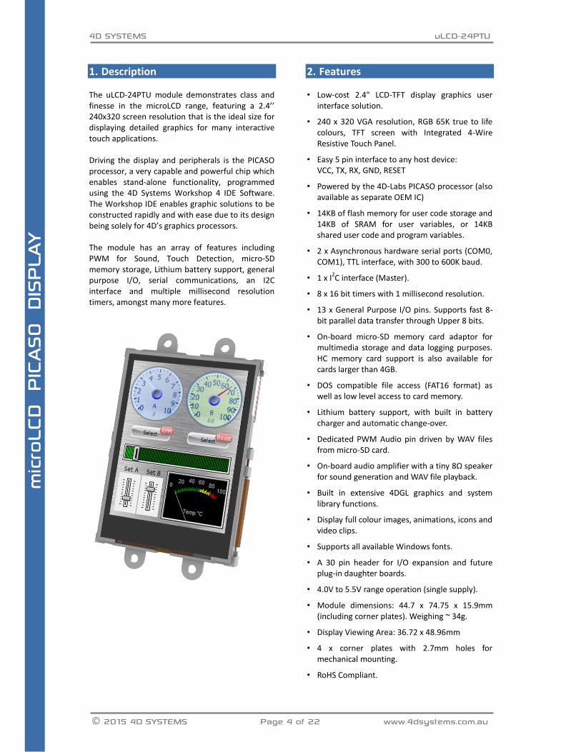
4D SYSTEMS uLCD-24PTU
© 2015 4D SYSTEMS Page 4 of 22 www.4dsystems.com.au
1. Description The uLCD-24PTU module demonstrates class and finesse in the microLCD range, featuring a 2.4’’ 240x320 screen resolution that is the ideal size for displaying detailed graphics for many interactive touch applications. Driving the display and peripherals is the PICASO processor, a very capable and powerful chip which enables stand-alone functionality, programmed using the 4D Systems Workshop 4 IDE Software. The Workshop IDE enables graphic solutions to be constructed rapidly and with ease due to its design being solely for 4D’s graphics processors. The module has an array of features including PWM for Sound, Touch Detection, micro-SD memory storage, Lithium battery support, general purpose I/O, serial communications, an I2C interface and multiple millisecond resolution timers, amongst many more features.
2. Features • Low-cost 2.4" LCD-TFT display graphics user
interface solution.
• 240 x 320 VGA resolution, RGB 65K true to life colours, TFT screen with Integrated 4-Wire Resistive Touch Panel.
• Easy 5 pin interface to any host device: VCC, TX, RX, GND, RESET
• Powered by the 4D-Labs PICASO processor (also available as separate OEM IC)
• 14KB of flash memory for user code storage and 14KB of SRAM for user variables, or 14KB shared user code and program variables.
• 2 x Asynchronous hardware serial ports (COM0, COM1), TTL interface, with 300 to 600K baud.
• 1 x I2C interface (Master).
• 8 x 16 bit timers with 1 millisecond resolution.
• 13 x General Purpose I/O pins. Supports fast 8-bit parallel data transfer through Upper 8 bits.
• On-board micro-SD memory card adaptor for multimedia storage and data logging purposes. HC memory card support is also available for cards larger than 4GB.
• DOS compatible file access (FAT16 format) as well as low level access to card memory.
• Lithium battery support, with built in battery charger and automatic change-over.
• Dedicated PWM Audio pin driven by WAV files from micro-SD card.
• On-board audio amplifier with a tiny 8Ω speaker for sound generation and WAV file playback.
• Built in extensive 4DGL graphics and system library functions.
• Display full colour images, animations, icons and video clips.
• Supports all available Windows fonts.
• A 30 pin header for I/O expansion and future plug-in daughter boards.
• 4.0V to 5.5V range operation (single supply).
• Module dimensions: 44.7 x 74.75 x 15.9mm (including corner plates). Weighing ~ 34g.
• Display Viewing Area: 36.72 x 48.96mm
• 4 x corner plates with 2.7mm holes for mechanical mounting.
• RoHS Compliant.
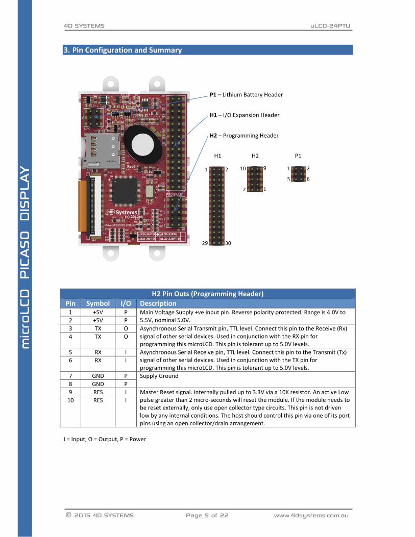
4D SYSTEMS uLCD-24PTU
© 2015 4D SYSTEMS Page 5 of 22 www.4dsystems.com.au
3. Pin Configuration and Summary
H2 Pin Outs (Programming Header)
Pin Symbol I/O Description 1 +5V P Main Voltage Supply +ve input pin. Reverse polarity protected. Range is 4.0V to
5.5V, nominal 5.0V. 2 +5V P
3 TX O Asynchronous Serial Transmit pin, TTL level. Connect this pin to the Receive (Rx) signal of other serial devices. Used in conjunction with the RX pin for programming this microLCD. This pin is tolerant up to 5.0V levels.
4 TX O
5 RX I Asynchronous Serial Receive pin, TTL level. Connect this pin to the Transmit (Tx) signal of other serial devices. Used in conjunction with the TX pin for programming this microLCD. This pin is tolerant up to 5.0V levels.
6 RX I
7 GND P Supply Ground
8 GND P
9 RES I Master Reset signal. Internally pulled up to 3.3V via a 10K resistor. An active Low pulse greater than 2 micro-seconds will reset the module. If the module needs to be reset externally, only use open collector type circuits. This pin is not driven low by any internal conditions. The host should control this pin via one of its port pins using an open collector/drain arrangement.
10 RES I
I = Input, O = Output, P = Power
P1 – Lithium Battery Header
H1 – I/O Expansion Header
H2 – Programming Header
H1 H2 P1
1
29
2
30
10
2
9
1
1
5
2
6
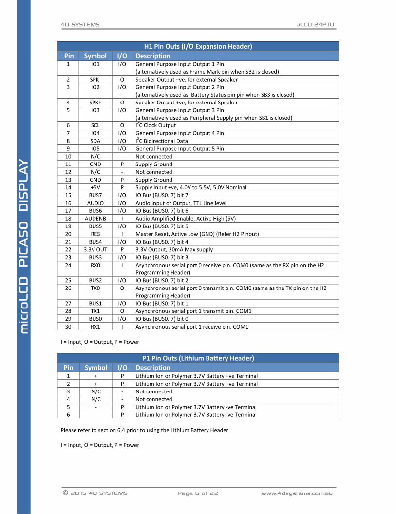
4D SYSTEMS uLCD-24PTU
© 2015 4D SYSTEMS Page 6 of 22 www.4dsystems.com.au
I = Input, O = Output, P = Power
Please refer to section 6.4 prior to using the Lithium Battery Header I = Input, O = Output, P = Power
H1 Pin Outs (I/O Expansion Header)
Pin Symbol I/O Description 1 IO1 I/O General Purpose Input Output 1 Pin
(alternatively used as Frame Mark pin when SB2 is closed)
2 SPK- O Speaker Output –ve, for external Speaker
3 IO2 I/O General Purpose Input Output 2 Pin (alternatively used as Battery Status pin pin when SB3 is closed)
4 SPK+ O Speaker Output +ve, for external Speaker
5 IO3 I/O General Purpose Input Output 3 Pin (alternatively used as Peripheral Supply pin when SB1 is closed)
6 SCL O I2C Clock Output
7 IO4 I/O General Purpose Input Output 4 Pin
8 SDA I/O I2C Bidirectional Data
9 IO5 I/O General Purpose Input Output 5 Pin
10 N/C - Not connected
11 GND P Supply Ground
12 N/C - Not connected
13 GND P Supply Ground
14 +5V P Supply Input +ve, 4.0V to 5.5V, 5.0V Nominal
15 BUS7 I/O IO Bus (BUS0..7) bit 7
16 AUDIO I/O Audio Input or Output, TTL Line level
17 BUS6 I/O IO Bus (BUS0..7) bit 6
18 AUDENB I Audio Amplified Enable, Active High (5V)
19 BUS5 I/O IO Bus (BUS0..7) bit 5
20 RES I Master Reset, Active Low (GND) (Refer H2 Pinout)
21 BUS4 I/O IO Bus (BUS0..7) bit 4
22 3.3V OUT P 3.3V Output, 20mA Max supply
23 BUS3 I/O IO Bus (BUS0..7) bit 3
24 RX0 I Asynchronous serial port 0 receive pin. COM0 (same as the RX pin on the H2 Programming Header)
25 BUS2 I/O IO Bus (BUS0..7) bit 2
26 TX0 O Asynchronous serial port 0 transmit pin. COM0 (same as the TX pin on the H2 Programming Header)
27 BUS1 I/O IO Bus (BUS0..7) bit 1
28 TX1 O Asynchronous serial port 1 transmit pin. COM1
29 BUS0 I/O IO Bus (BUS0..7) bit 0
30 RX1 I Asynchronous serial port 1 receive pin. COM1
P1 Pin Outs (Lithium Battery Header)
Pin Symbol I/O Description 1 + P Lithium Ion or Polymer 3.7V Battery +ve Terminal
2 + P Lithium Ion or Polymer 3.7V Battery +ve Terminal
3 N/C - Not connected
4 N/C - Not connected
5 - P Lithium Ion or Polymer 3.7V Battery -ve Terminal
6 - P Lithium Ion or Polymer 3.7V Battery -ve Terminal

4D SYSTEMS uLCD-24PTU
© 2015 4D SYSTEMS Page 7 of 22 www.4dsystems.com.au
4. Hardware Interface - Pins The uLCD-24PTU provides both a hardware and software interface. This section describes in detail the hardware interface pins of the device.
Serial Ports - COM0, COM1 UARTS 4.1. The uLCD-24PTU has two dedicated hardware Asynchronous Serial ports that can communicate with external serial devices. These are referred to as the COM0 and the COM1 serial ports. The primary features are: • Full-Duplex 8 bit data transmission and
reception. • Data format: 8 bits, No Parity, 1 Stop bit. • Independent Baud rates from 300 baud up to
600K baud. • Single byte transmits and receives or a fully
buffered service. The buffered service feature runs in the background capturing and buffering serial data without the user application having to constantly poll any of the serial ports. This frees up the application to service other tasks.
A single byte serial transmission consists of the start bit, 8-bits of data followed by the stop bit. The start bit is always 0, while a stop bit is always 1. The LSB (Least Significant Bit, Bit 0) is sent out first following the start bit. Figure below shows a single byte transmission timing diagram.
COM0 is also the primary interface for 4DGL user program downloads and chip configuration (PmmC programming). Once the compiled 4DGL application program (EVE byte-code) is downloaded and the user code starts executing, the serial port is then available to the user application. Refer to Section 5. ‘Firmware / PmmC Programming’ for more details on this subject.
TX0 pin (Serial Transmit COM0): Asynchronous Serial port COM0 transmit pin, TX0. Connect this pin to external serial device receive (Rx) signal. This pin is 5.0V tolerant. RX0 pin (Serial Receive COM0): Asynchronous Serial port COM0 receive pin, RX0. Connect this pin to external serial device transmit (Tx) signal. This pin is 5.0V tolerant. TX1 pin (Serial Transmit COM1): Asynchronous Serial port COM1 transmit pin, TX1. Connect this pin to external serial device receive (Rx) signal. This pin is 5.0V tolerant. RX1 pin (Serial Receive COM1): Asynchronous Serial port COM1 receive pin, RX1. Connect this pin to external serial device transmit (Tx) signal. This pin is 5.0V tolerant.
General Purpose I/O 4.2. There are 13 general purpose Input/Output (GPIO) pins available to the user. These are grouped as IO1..IO5 (Note for IO1, IO2 and IO3 below) and BUS0..BUS7. Power-Up Reset default is all INPUTS. The 5 I/O pins (IO1..IO5), provide flexibility of individual bit operations while the 8 pins (BUS0..BUS7), known as GPIO BUS, serve collectively for byte wise operations. The IO4 and IO5 also act as strobing signals to control the GPIO Bus. GPIO Bus can be read or written by strobing a low pulse (50ns duration or greater) the IO4/BUS_RD or IO5/BUS_WR for read or write respectively. For detailed usage refer to the separate document titled: “PICASO-4DGL-Internal-Functions.pdf” IO1-IO5 pins: General purpose I/O pins. Each pin can be individually set for INPUT or an OUTPUT. IO1-IO3 have also optional functionality when its dedicated Solder Jumper is closed. Please read below for more information. IO1 pin (Frame Mark pin): The IO1 pin has 2 functions. It can be used as a GPIO pin (Default on HW >= 13.0 onward) but can also be used to detect the start of a Frame (Default on HW < 13.0). When used as a Frame Mark pin, simply solder it´s dedicated solder jumper SB2. When using IO1 for Frame Mark read the status of IO1 as an Input. IO2 pin (Lithium Battery Status pin): The IO2 pin has 2 functions. It can be used as a

4D SYSTEMS uLCD-24PTU
© 2015 4D SYSTEMS Page 8 of 22 www.4dsystems.com.au
GPIO pin (Default on HW >= 13.0) but can also be used to tell when the Lithium battery has reached a low level (3.7V) and needs to be charged (Default on HW < 13.0). When used as a Lithium Battery Status pin, simply solder it´s dedicated solder jumper SB3. When using IO2 for Battery Status read the status of IO2 as an Input. (See 6.4. ‘Lithium Batteries’ for more information). IO3 pin (Peripheral Supply pin): The IO3 pin has 2 functions. It can be used as a GPIO pin (Default HW >= 13.0) but can also be used as Peripheral Supply pin (Default HW < 13.0) when it´s dedicated solder jumper SB1 is closed. IO3 set as Peripheral Supply pin is controllable via the processor, or via the H2 Interface pin driven by an external circuit. If IO3 is set as OUTPUT and driven HIGH the uSD card and Display are enabled, and disabled when driven LO. Set as INPUT to use an external circuit to drive this pin. IO4/BUS_RD pin (GPIO IO4 or BUS_RD pin): General Purpose IO4 pin. Also used for BUS_RD signal to read and latch the data in to the parallel GPIO BUS0..BUS7. IO5/BUS_WR pin (GPIO IO5 or BUS_WR pin): General Purpose IO5 pin. Also used for BUS_WR signal to write and latch the data to the parallel GPIO BUS0..BUS7. BUS0-BUS7 pins (GPIO 8-Bit Bus): 8-bit parallel General purpose I/O Bus.
Note: All GPIO pins are 5.0V tolerant.
System Pins 4.3. +5V (Module Voltage Input) H1 pin 14, H2 pin 1 and 2: Module supply voltage input pin. This pin must be connected to a regulated supply voltage in the range of 4.0 Volts* to 5.5 Volts DC. Nominal operating voltage is 5.0 Volts. 3.3V Out (3.3V Regulated Output) H1 pin 22: External circuitry that requires a regulated 3.3V supply can be powered up via this pin. Maximum available current is 150mA. Attempting to draw more can result in peripherals such as the microSD card, not working correctly.
GND (Module Ground) H1 pin 11/13, H2 pin 7 and 8: Device ground pins. These pins must be connected to ground. RESET (Module Master Reset) H1 pin 20, H2 pin 9 and 10: Module Master Reset pin. An active low pulse of greater than 2μs will reset the module. Internally pulled up to 3.3V via a 10K resistor. Only use open collector type circuits to reset the device if an external reset is required. SPK-/SPK+ (External Speaker Outputs) H1 pin 2/4 respectively: External Speaker Outputs, designed to drive an 8Ω speaker to a maximum of 1.2W. These are connected in Parallel with the on board speaker. AUDENB (Audio Enable Output) H1 pin 18: Output dedicated to enable or disable an external amplifier if the on-board amplifier is not desirable to use. Controlled by the PICASO processor. When AUDENB is low, the on-board Amplifier is Enabled. When AUDENB is high, the on-board Amplifier is Disabled. AUDIO (Audio Line Level Input/Output) H1 pin 16: Universal Input or Output specifically for Audio. This pin connects directly into the on-board amplifier, but also with the filtered PWM output from the PICASO Processor. This pin can be used to input a signal into the on-board amplifier to play audio from an external device using the on-board amplifier, or as a line-level output to drive an external amplifier with PICASO generated Audio. Note that AUDENB must be enabled (low) in PICASO for any input signal to be heard. +/- (Lithium Battery Terminals) P1 pins 1/2(+ve), 5/6(-ve): These are the terminals of the Lithium Battery connector. These are to be connected only to a Lithium Ion or Polymer 3.7V Battery else the uLCD-24PTU may be damaged. See Section 6.4

4D SYSTEMS uLCD-24PTU
© 2015 4D SYSTEMS Page 9 of 22 www.4dsystems.com.au
5. PmmC/Firmware Programming The PICASO processor used in the uLCD-24PTU module is a custom graphics processor. All functionality including the high level commands are built into the chip. This chip level configuration is available as a Firmware/PmmC (Personality-module-micro-Code) file. A PmmC file contains all of the low level micro-code information (analogy of that of a soft silicon) which define the characteristics and functionality of the device. The ability of programming the device with a PmmC file provides an extremely flexible method of customising as well as upgrading it with future enhancements. A PmmC file can only be programmed into the device via its COM0 serial port. Figure below provides a typical implementation for the PmmC programming interface. The PmmC file is programmed into the device with the aid of Workshop 4, the 4D Systems IDE software (See Section 11). To provide a link between the PC and the ICSP interface, a specific 4D Programming Cable is required and is available from 4D Systems. Using a non-4D programming interface could damage your display, and void your Warranty. Please refer to section 8.1 for more information on 4D programming interfaces.
6. Module Features The uLCD-24PTU module is designed to accommodate most applications. Some of the main features of the module are listed below.
Display – 2.4” TFT Touch Screen 6.1. The uLCD-24PTU module is equipped with a 2.4” TFT display. Details of the display are listed below: • Screen Size: 2.4” diagonal • Resolution: 240 x 320 • Integrated 4-Wire Resistive Touch Screen • Screen Dimensions: 42.70 x 60.25 x 3.70mm • Viewing Area: 36.72 x 48.96mm • Pixel Pitch: 0.153 x 0.153mm • Brightness: 150cd/m2 • Contrast Ratio: 250:1 • Viewing Angle Above Centre: 20 degrees • Viewing Angle Below Centre: 35 degrees • Viewing Angle Left of Centre: 40 degrees • Viewing Angle Right of Centre: 40 degrees • Viewing Direction: 6 O'clock • 4 Parallel LEDs for Backlighting
Note: The Displays used are the highest rated ‘Grade A’ Displays, which allow for 0-4 defective pixels. A defective pixel could be solid Black (Dead), White, Red, Green or Blue.
PICASO Processor 6.2. The module is designed around the PICASO Graphics Controller from 4D-Labs.
The PICASO is a smart Controller and the interface to the TFT- LCD displays is almost plug-n-play. All of the data and control signals are provided by the chip to interface directly to the display. Powerful graphics, text, image, animation and countless more features are built right inside the chip.
4D Programming Cable

4D SYSTEMS uLCD-24PTU
© 2015 4D SYSTEMS Page 10 of 22 www.4dsystems.com.au
The data sheet for the processor is available from the http://www.4dsystems.com.au website: “PICASO-Processor-Datasheet-REVx.pdf”
Audio 6.3. Audio playback support in the PICASO Processor enables the uLCD-24PTU module to play audio WAV files stored in the micro-SD memory card. PWM and an on-board audio amplifier with 8Ω speaker ensure ample audio output capability. A simple instruction enables the user to play/pause/stop audio files while continuing the execution of the user application code, such as display updates, touch recognition, communications, etc. The audio system also allows real time pitch change of audio samples. For a complete list of audio commands please refer to the separate document titled: “PICASO-4DGL-Internal-Functions.pdf”
Note: The on-board speaker is a small device designed to project into an audio cavity. It is not very loud by itself. To enable louder audio, it is recommended to use a larger external 8Ω speaker. See the ‘Hardware Interface Pins’ – ‘System Pins’ section for more information.
Lithium Batteries 6.4. The uLCD-24PTU module includes a battery charging circuit suitable for Lithium Ion (LiIon) and Lithium Polymer (LiPo) batteries, which is designed to work only with 3.7V batteries. If anything other than a LiIon or LiPo 3.7V battery is connected the module could be damaged. Features current sensing and reverse discharge protection using an on board Lithium charge management controller. When the Lithium battery is connected and an external source (4.5V minimum) is connected to either of the +5V pins, the Lithium battery will be charged automatically. If the 5V source is disconnected, the Lithium battery will be switched in circuit and continue to power the module automatically. Charge voltage = 4.2V, Charge current = ~210mA When running from the Lithium battery, when the battery level drops down to ~3.7V, the Status input (connected to IO2) into the Picaso will be triggered indicating the battery is discharged. The display should then be connected to an external
5V source for charging. When the battery is at this cut off voltage, uSD card read and write operations should be avoided, as they may fail due to low voltage. It is up to the User to handle the operation of the display module when using a Lithium Battery. WARNING: There is a large range of Lithium batteries available on the market. Some include safety circuits built in, while others do not. Lithium batteries can explode if short circuited, overcharged, if they get too hot, and can leak if they sit fully discharged for a prolonged period. 4D Systems recommends whenever Lithium batteries are used that caution and due diligence should be exercised to ensure the safety of the user and nearby people. While the chances of explosion or leakage may be minimal, 4D Systems recommends safe practices at all times when dealing with these batteries. If Lithium Batteries are powering the module, it is highly recommended to periodically monitor the STAT pin. If the module is put to sleep, periodically wake the module to check the STAT pin.
SD/SDHC Memory Cards 6.5. The module supports micro-SD memory cards via the on-board micro-SD connector. The memory card is used for all multimedia file retrieval such as images, animations and movie clips. The memory card can also be used as general purpose storage for data logging applications. Support is available for off the shelf micro-SD and high capacity HC memory cards (4GB and above).
Note: A microSD card capable of SPI is a requirement for all 4D Systems’ display modules powered by Goldelox, Picaso or Diablo16 Processors. If a non-SPI compatible card is used, it will simply fail to mount, or may cause intermittent issues resulting in lock ups and crashing of the application. Please refer to the 4D Systems website for microSD cards offered by 4D Systems.
FAT16 6.6. The uLCD-24PTU uses off the shelf standard SDHC/SD/micro-SD memory cards with up to 2GB capacity usable with FAT16 formatting. For any FAT file related operations, before the memory card can be used it must first be formatted with
4D SYSTEMS uLCD-24PTU
© 2015 4D SYSTEMS Page 11 of 22 www.4dsystems.com.au
FAT16 option. The formatting of the card can be done on any PC system with a card reader. Select the appropriate drive and choose the FAT16 (or just FAT in some systems) option when formatting. The card is now ready to be used in the PICASO based application. The uLCD-24PTU also supports high capacity HC memory cards (4GB and above). The available capacity of SD-HC cards varies according to the way the card is partitioned and the commands used to access it. The FAT partition is always first (if it exists) and can be up to the maximum size permitted by FAT16. Windows 7 will format FAT16 up to 4GB. Windows XP will format FAT16 up to 2GB and the Windows XP command prompt will format FAT16 up to 4GB.
7. Display Precautions
• Avoid having to display the same image/object on the screen for lengthy periods of time. This will cause a burn-in which is a common problem with all types of display technologies. Blank the screen after a while or dim it very low by adjusting the contrast. Better still; implement a screen saver feature. • Moisture and water can damage the display. Moisture on the surface of a powered display will cause the electrodes to corrode. Wipe off any moisture gently or let the display dry before usage.
• Dirt from fingerprint oil and fat can easily stain the surface of the display. Gently wipe off any stains with a soft lint-free cloth.
• The performance of the display will degrade under high temperature and humidity. Avoid such conditions when storing. • Do not tamper with the display flex cable that is connected to the control board. This may affect the connection between the display and the driving circuitry and cause failure. • Displays are susceptible to mechanical shock and any force exerted on the module may result in deformed zebra stripes, a cracked display cell and broken backlight • Always use the mounting holes on the module's corner plates to mount the display.
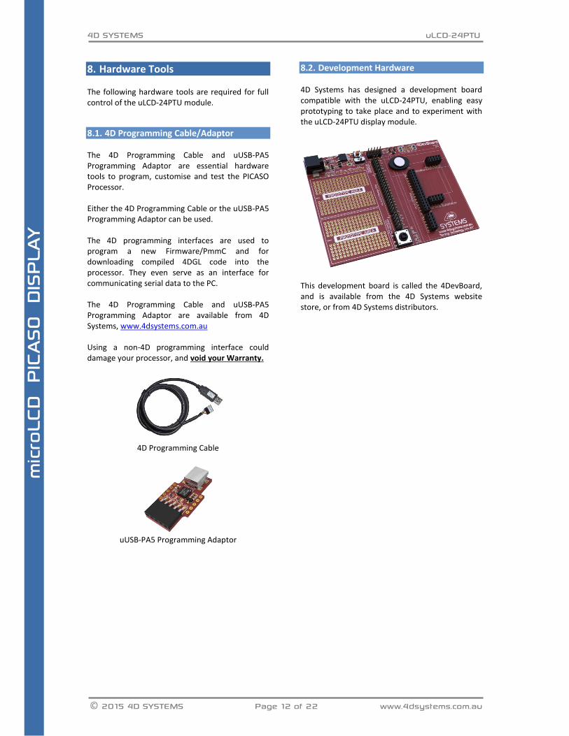
4D SYSTEMS uLCD-24PTU
© 2015 4D SYSTEMS Page 12 of 22 www.4dsystems.com.au
8. Hardware Tools The following hardware tools are required for full control of the uLCD-24PTU module.
4D Programming Cable/Adaptor 8.1. The 4D Programming Cable and uUSB-PA5 Programming Adaptor are essential hardware tools to program, customise and test the PICASO Processor. Either the 4D Programming Cable or the uUSB-PA5 Programming Adaptor can be used. The 4D programming interfaces are used to program a new Firmware/PmmC and for downloading compiled 4DGL code into the processor. They even serve as an interface for communicating serial data to the PC. The 4D Programming Cable and uUSB-PA5 Programming Adaptor are available from 4D Systems, www.4dsystems.com.au Using a non-4D programming interface could damage your processor, and void your Warranty.
4D Programming Cable
uUSB-PA5 Programming Adaptor
Development Hardware 8.2. 4D Systems has designed a development board compatible with the uLCD-24PTU, enabling easy prototyping to take place and to experiment with the uLCD-24PTU display module.
This development board is called the 4DevBoard, and is available from the 4D Systems website store, or from 4D Systems distributors.
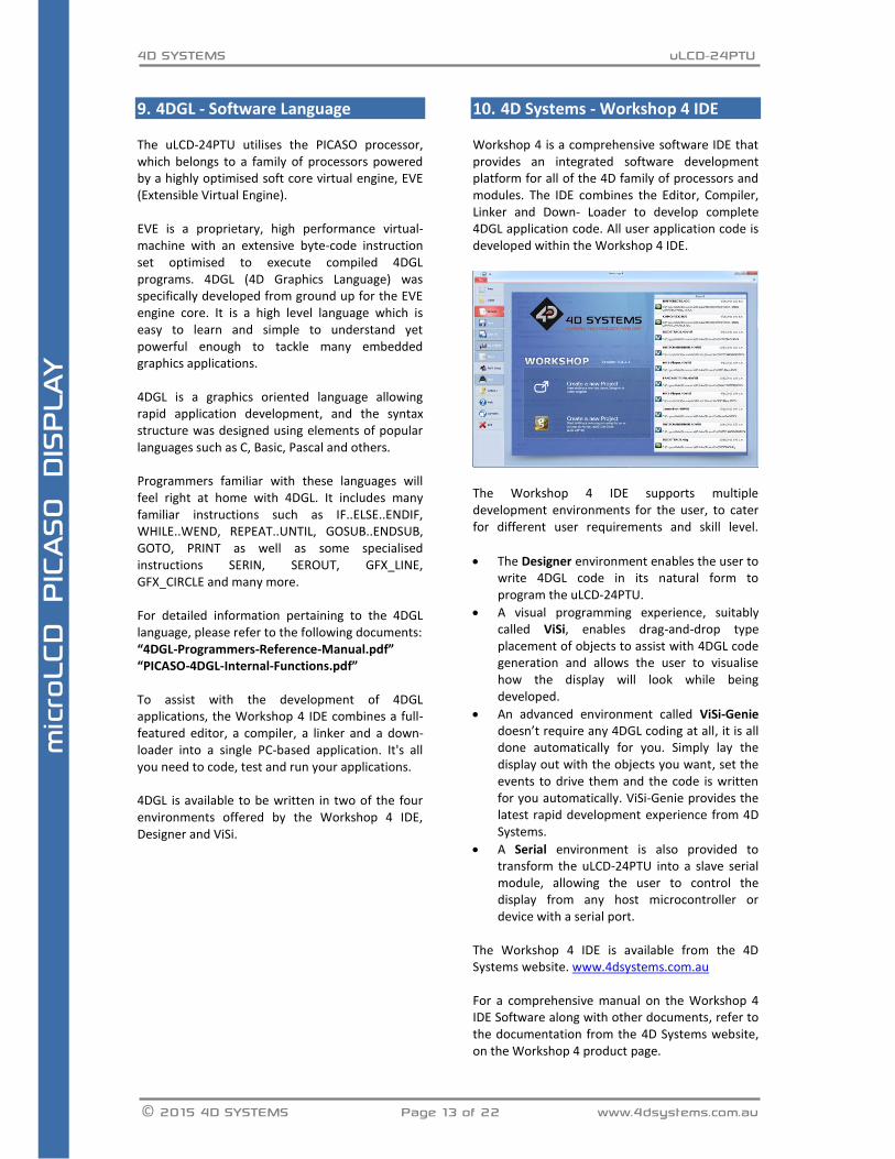
4D SYSTEMS uLCD-24PTU
© 2015 4D SYSTEMS Page 13 of 22 www.4dsystems.com.au
9. 4DGL - Software Language The uLCD-24PTU utilises the PICASO processor, which belongs to a family of processors powered by a highly optimised soft core virtual engine, EVE (Extensible Virtual Engine). EVE is a proprietary, high performance virtual-machine with an extensive byte-code instruction set optimised to execute compiled 4DGL programs. 4DGL (4D Graphics Language) was specifically developed from ground up for the EVE engine core. It is a high level language which is easy to learn and simple to understand yet powerful enough to tackle many embedded graphics applications. 4DGL is a graphics oriented language allowing rapid application development, and the syntax structure was designed using elements of popular languages such as C, Basic, Pascal and others. Programmers familiar with these languages will feel right at home with 4DGL. It includes many familiar instructions such as IF..ELSE..ENDIF, WHILE..WEND, REPEAT..UNTIL, GOSUB..ENDSUB, GOTO, PRINT as well as some specialised instructions SERIN, SEROUT, GFX_LINE, GFX_CIRCLE and many more. For detailed information pertaining to the 4DGL language, please refer to the following documents: “4DGL-Programmers-Reference-Manual.pdf” “PICASO-4DGL-Internal-Functions.pdf” To assist with the development of 4DGL applications, the Workshop 4 IDE combines a full-featured editor, a compiler, a linker and a down-loader into a single PC-based application. It's all you need to code, test and run your applications. 4DGL is available to be written in two of the four environments offered by the Workshop 4 IDE, Designer and ViSi.
10. 4D Systems - Workshop 4 IDE Workshop 4 is a comprehensive software IDE that provides an integrated software development platform for all of the 4D family of processors and modules. The IDE combines the Editor, Compiler, Linker and Down- Loader to develop complete 4DGL application code. All user application code is developed within the Workshop 4 IDE.
The Workshop 4 IDE supports multiple development environments for the user, to cater for different user requirements and skill level.
The Designer environment enables the user to write 4DGL code in its natural form to program the uLCD-24PTU.
A visual programming experience, suitably called ViSi, enables drag-and-drop type placement of objects to assist with 4DGL code generation and allows the user to visualise how the display will look while being developed.
An advanced environment called ViSi-Genie doesn’t require any 4DGL coding at all, it is all done automatically for you. Simply lay the display out with the objects you want, set the events to drive them and the code is written for you automatically. ViSi-Genie provides the latest rapid development experience from 4D Systems.
A Serial environment is also provided to transform the uLCD-24PTU into a slave serial module, allowing the user to control the display from any host microcontroller or device with a serial port.
The Workshop 4 IDE is available from the 4D Systems website. www.4dsystems.com.au For a comprehensive manual on the Workshop 4 IDE Software along with other documents, refer to the documentation from the 4D Systems website, on the Workshop 4 product page.
4D SYSTEMS uLCD-24PTU
© 2015 4D SYSTEMS Page 14 of 22 www.4dsystems.com.au
Workshop 4 – Designer Environment 10.1. Choose the Designer environment to write 4DGL code in its raw form. The Designer environment provides the user with a simple yet effective programming environment where pure 4DGL code can be written, compiled and downloaded to the uLCD-24PTU.
Workshop 4 – ViSi Environment 10.2. ViSi was designed to make the creation of graphical displays a more visual experience. ViSi is a great software tool that allows the user to see the instant results of their desired graphical layout. Additionally, there is a selection of inbuilt dials, gauges and meters that can simply be placed onto the simulated module display. From here each object can have its properties edited, and at the click of a button all relevant 4DGL code associated with that object is produced in the user program. The user can then write 4DGL code around these objects to utilise them in the way they choose.
Workshop 4 – ViSi Genie Environment 10.3. ViSi Genie is a breakthrough in the way 4D Systems’ graphic display modules are programmed. It is an environment like no other, a code-less programming environment that provides the user with a rapid visual experience, enabling a simple GUI application to be ‘written’ from scratch in literally seconds. ViSi Genie does all the background coding, no 4DGL to learn, it does it all for you. Pick and choose the relevant objects to place on the display, much like the ViSi Environment (See Section 11.2), yet without having to write a single line of code. Each object has parameters which can be set, and configurable events to animate and drive other objects or communicate with external devices. Simply place an object on the screen, position and size it to suit, set the parameters such as colour, range, text, and finally select the event you wish the object to be associated with, it is that simple. In seconds you can transform a blank display into a fully animated GUI with moving sliders, animated press and release buttons, and much more. All without writing a single line of code! ViSi Genie provides the user with a feature rich rapid development environment, second to none.
Workshop 4 – Serial Environment 10.4. The Serial environment in the Workshop 4 IDE provides the user the ability to transform the uLCD-24PTU into a slave serial graphics controller. This enables the user to use their favourite microcontroller or serial device as the Host, without having to learn 4DGL or program in a separate IDE. Once the uLCD-24PTU is configured

4D SYSTEMS uLCD-24PTU
© 2015 4D SYSTEMS Page 15 of 22 www.4dsystems.com.au
and downloaded to from the Serial Environment, simple graphic commands can be sent from the users host microcontroller to display primitives, images, sound or even video. Refer to the “Serial Command Set Reference Manual” from the Workshop 4 product page on the 4D Systems website for a complete listing of all the supported serial commands By default, each module shipped from the 4D Systems factory will come pre-programmed ready for use in the Serial mode.
11. Starter Kit 4D Systems highly recommends all first time buyers of 4D Systems’ displays, to purchase the Starter Kit when purchasing their first 4D Systems display solution. The Starter Kit provides all the hardware that is required to get the user up and running. Not all development environments and features will be needed by every user, however by purchasing the display solution in a Starter Kit, it ensures that if you want to take full advantage of the 4D Systems display solution and try out each of the 4D Workshop4 Environments, upgrade PmmC/firmware, you can. The Designer environment can utilise every feature of the display, however depending on the user requirements, a micro-SD (uSD) card may not be required. The uSD card is used when displaying images/video/sound, along with datalogging to uSD, and a programming cable is definitely required for downloading compiled code and PmmC/Firmware updates. The ViSi environment is the same as Designer in terms of feature utilisation, but is image based so requires a uSD card, along with a programming cable. The ViSi-Genie environment is also image based, and therefore requires a uSD card and programming cable also. The Serial environment does not require either a uSD or Programming cable to be used, however can utilise both depending on the user requirements. The uSD card can be used for such things as storage of multimedia files and datalogging, and the Programming cable for PmmC/Firmware updates, or changing to one of the other three programming environments. The Starter Kit includes:
4D Programming Adaptor or Cable
2Gb microSD Card
5 way cable for easy connection to a breadboard or host
Display Module
Quick Start Guide Simply select the Starter Kit option when purchasing the chosen display module on the 4D Systems shopping cart, or from your local distributor.
4D SYSTEMS uLCD-24PTU
© 2015 4D SYSTEMS Page 16 of 22 www.4dsystems.com.au
12. Notes ________________________________________________________________________________________________________________________________________________________________________________________________________________________________________________________________________________________________________________________________________________________________________ ________________________________________________________________________________________________________________________________________________________________________________________________________________________________________________________________________________________________________________________________________________________________________ ________________________________________________________________________________________________________________________________________________________________________________________________________________________________________________________________________________________________________________________________________________________________________ ________________________________________________________________________________________________________________________________________________________________________________________________________________________________________________________________________________________________________________________________________________________________________ ________________________________________________________________________________________________________________________________________________________________________________________________________________________________________________________________________________________________________________________________________________________________________ ________________________________________________________________________________________________________________________________________________________________________________________________________________________________________________________________________________________________________________________________________________________________________ ________________________________________________________________________________________________________________________________________________________________________________________________________________________________________________________________________________________________________________________________________________________________________ ________________________________________________________________________________________________________________________________________________________________________________________________________________________________________________________________________________________________________________________________________________________________________ ________________________________________________________________________________________________________________________________________________________________________________________________________________________________________________________________________________________________________________________________________________________________________ ________________________________________________________________________________________________________________________________________________________________________________________________________________________________________________________________________________________________________________________________________________________________________ ________________________________________________________________________________________________________________________________________________________________________________________________________________________________________________________________________________________________________________________________________________________________________ ________________________________________________________________________________________________________________________________________________________________________________________________________________________________________________________________________________________________________________________________________________________________________ ____________________________________________________________________________________________________________________________________________________________________________________________________________________________________________________________________________________________________________________________________________________________________________________________________________________________________________________________________________________________________________________________________________________________
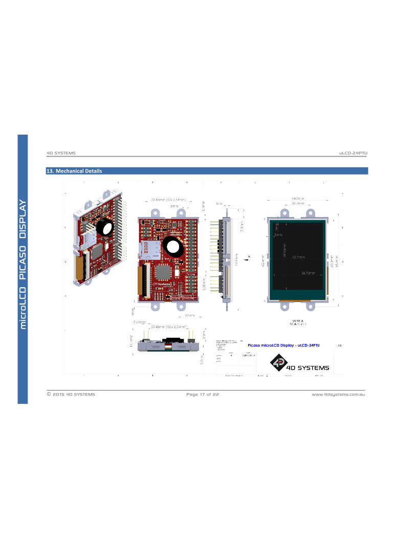
4D SYSTEMS uLCD-24PTU
© 2015 4D SYSTEMS Page 17 of 22 www.4dsystems.com.au
13. Mechanical Details
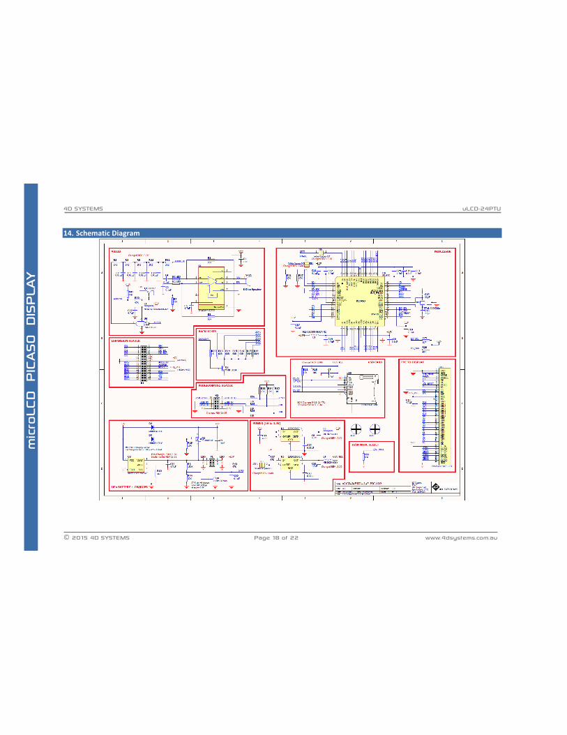
4D SYSTEMS uLCD-24PTU
© 2015 4D SYSTEMS Page 18 of 22 www.4dsystems.com.au
14. Schematic Diagram

4D SYSTEMS uLCD-24PTU
© 2015 4D SYSTEMS Page 19 of 22 www.4dsystems.com.au
15. Specifications and Ratings
ABSOLUTE MAXIMUM RATINGS
Operating ambient temperature ................................................................................................... -15°C to +65°C
Storage temperature .......................................................................................................................... -30°C +70°C
Voltage on any digital input pin with respect to GND ....................................................................... -0.3V to 6.0V
Voltage on SWITCH pin with respect to GND ................................................................................... -0.3V to 6.0V
Voltage on VCC with respect to GND ................................................................................................. -0.3V to 6.0V
NOTE: Stresses above those listed here may cause permanent damage to the device. This is a stress rating only and functional operation of the device at those or any other conditions above those indicated in the recommended operation listings of this specification is not implied. Exposure to maximum rating conditions for extended periods may affect device reliability.
RECOMMENDED OPERATING CONDITIONS
Parameter Conditions Min Typ Max Units
Supply Voltage (VCC) 4.0 5.0 5.5 V
Operating Temperature -10 -- +60 °C
Input Low Voltage (VIL) VCC = 3.3V, all pins VGND -- 0.2VCC V
Input High Voltage (VIH) VCC = 3.3V, non 5V tolerant pins 0.8VCC -- VCC V
Input High Voltage (VIH) All GPIO pins, RX0 and TX0 pins 0.8VCC -- 5.5 V
Reset Pulse External Open Collector 2.0 -- -- µs
Operational Delay Power-Up or External Reset 500 -- 3000 ms
GLOBAL CHARACTERISTICS BASED ON OPERATING CONDITIONS
Parameter Conditions Min Typ Max Units
Supply Current (ICC) VCC = 5.0V, heavily depends on screen usage conditions, sleep mode
10 125 220 mA
Output Low Voltage (VOL)
VCC = 5.0V, IOL = 3.4mA -- -- 0.4 V
Output High Voltage (VOH)
VCC = 5.0V, IOL = -2.0mA 2.4 -- -- V
Capacitive Loading All pins -- -- 50 pF
Flash Memory Endurance
PICASO PmmC Programming -- 10000 -- E/W
TOUCH SCREEN CHARACTERISTICS
Parameter Conditions Min Typ Max Units
Linearity -- -- <1.5 %
Terminal Resistance X X film side 300 400 800 Ohm
Terminal Resistance Y Y film side 300 600 800 Ohm
Durability – Scratch Test Stylus Pen or Finger Sliding 100 -- -- K
Durability – Tap Test Stylus Pen or Finger Press 1 -- -- Million
Transparency Non Glare 80 -- -- %
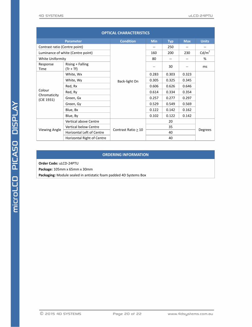
4D SYSTEMS uLCD-24PTU
© 2015 4D SYSTEMS Page 20 of 22 www.4dsystems.com.au
OPTICAL CHARACTERISTICS
Parameter Condition Min Typ Max Units
Contrast ratio (Centre point)
Back-light On
-- 250 -- --
Luminance of white (Centre point) 160 200 230 Cd/m2
White Uniformity 80 -- -- %
Response Time
Rising + Falling (Tr + Tf)
-- 30 -- ms
Colour Chromaticity (CIE 1931)
White, Wx 0.283 0.303 0.323
White, Wy 0.305 0.325 0.345
Red, Rx 0.606 0.626 0.646
Red, Ry 0.614 0.334 0.354
Green, Gx 0.257 0.277 0.297
Green, Gy 0.529 0.549 0.569
Blue, Bx 0.122 0.142 0.162
Blue, By 0.102 0.122 0.142
Viewing Angle
Vertical above Centre
Contrast Ratio > 10
20
Degrees Vertical below Centre 35
Horizontal Left of Centre 40
Horizontal Right of Centre 40
ORDERING INFORMATION
Order Code: uLCD-24PTU
Package: 105mm x 65mm x 30mm
Packaging: Module sealed in antistatic foam padded 4D Systems Box
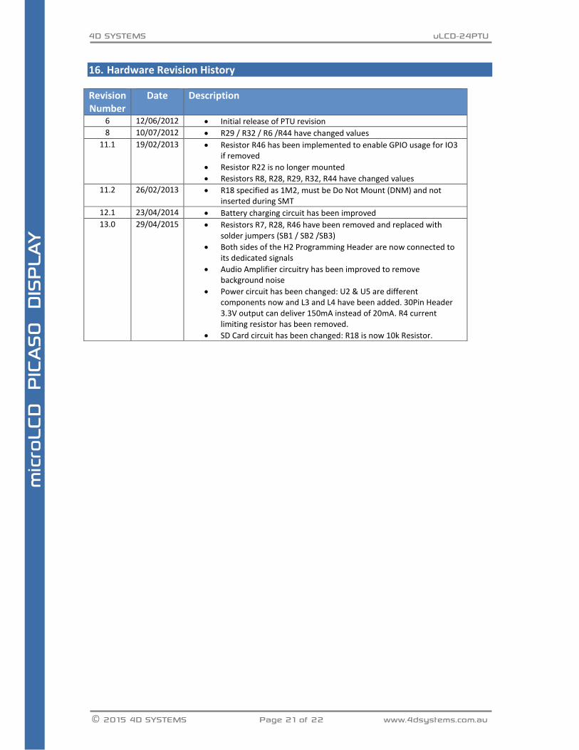
4D SYSTEMS uLCD-24PTU
© 2015 4D SYSTEMS Page 21 of 22 www.4dsystems.com.au
16. Hardware Revision History
Revision Number
Date Description
6 12/06/2012 Initial release of PTU revision
8 10/07/2012 R29 / R32 / R6 /R44 have changed values
11.1 19/02/2013 Resistor R46 has been implemented to enable GPIO usage for IO3 if removed
Resistor R22 is no longer mounted
Resistors R8, R28, R29, R32, R44 have changed values
11.2 26/02/2013 R18 specified as 1M2, must be Do Not Mount (DNM) and not inserted during SMT
12.1 23/04/2014 Battery charging circuit has been improved
13.0 29/04/2015 Resistors R7, R28, R46 have been removed and replaced with solder jumpers (SB1 / SB2 /SB3)
Both sides of the H2 Programming Header are now connected to its dedicated signals
Audio Amplifier circuitry has been improved to remove background noise
Power circuit has been changed: U2 & U5 are different components now and L3 and L4 have been added. 30Pin Header 3.3V output can deliver 150mA instead of 20mA. R4 current limiting resistor has been removed.
SD Card circuit has been changed: R18 is now 10k Resistor.

4D SYSTEMS uLCD-24PTU
© 2015 4D SYSTEMS Page 22 of 22 www.4dsystems.com.au
17. Legal Notice Proprietary Information The information contained in this document is the property of 4D Systems Pty. Ltd. and may be the subject of patents pending or granted, and must not be copied or disclosed without prior written permission. 4D Systems endeavours to ensure that the information in this document is correct and fairly stated but does not accept liability for any error or omission. The development of 4D Systems products and services is continuous and published information may not be up to date. It is important to check the current position with 4D Systems. 4D Systems reserves the right to modify, update or makes changes to Specifications or written material without prior notice at any time. All trademarks belong to their respective owners and are recognised and acknowledged. Disclaimer of Warranties & Limitation of Liability 4D Systems makes no warranty, either expressed or implied with respect to any product, and specifically disclaims all other warranties, including, without limitation, warranties for merchantability, non-infringement and fitness for any particular purpose. Information contained in this publication regarding device applications and the like is provided only for your convenience and may be superseded by updates. It is your responsibility to ensure that your application meets with your specifications. Images and graphics used throughout this document are for illustrative purposes only. All images and graphics used are possible to be displayed on the 4D Systems range of products, however the quality may vary. In no event shall 4D Systems be liable to the buyer or to any third party for any indirect, incidental, special, consequential, punitive or exemplary damages (including without limitation lost profits, lost savings, or loss of business opportunity) arising out of or relating to any product or service provided or to be provided by 4D Systems, or the use or inability to use the same, even if 4D Systems has been advised of the possibility of such damages. 4D Systems products are not fault tolerant nor designed, manufactured or intended for use or resale as on line control equipment in hazardous environments requiring fail – safe performance, such as in the operation of nuclear facilities, aircraft navigation or communication systems, air traffic control, direct life support machines or weapons systems in which the failure of the product could lead directly to death, personal injury or severe physical or environmental damage (‘High Risk Activities’). 4D Systems and its suppliers specifically disclaim any expressed or implied warranty of fitness for High Risk Activities. Use of 4D Systems’ products and devices in 'High Risk Activities' and in any other application is entirely at the buyer’s risk, and the buyer agrees to defend, indemnify and hold harmless 4D Systems from any and all damages, claims, suits, or expenses resulting from such use. No licenses are conveyed, implicitly or otherwise, under any 4D Systems intellectual property rights.
18. Contact Information
For Technical Support: [email protected]
For Sales Support: [email protected]
Website: www.4dsystems.com.au
Copyright 4D Systems Pty. Ltd. 2000-2015.
Reference available by request
Zohaib Arshad https://www.linkedin.com/in/arshadzohaib
4920 Sorento Road, Sacramento, CA, 95835 (916) 388 - 4433 [email protected] OBJECTIVE:
Engineering position to apply my technical abilities and education.
EDUCATION: Bachelors of Science Expected Graduation: Spring 2016 Electrical and Electronics Engineering, CSU Sacramento
RELATED COURSES:
Electronics II* Power System Analysis Probability and Random Signals CMOS and VLSI Design* Modern Communication System Signal Processing and Linear Systems Feedback Systems* Microprocessor Design Applied Electromagnetics
KNOWLEDGE AND SKILLS
Programming (Familiar): PHP • C/C++ Software Applications: MS Office 2003 – 2013 • Cadence PSpice • Cadence Virtuoso • Quartus II • ModelSim-Altera • NI
Multisim 13.0 Operating Systems: Windows 10 • Windows 7 • OS X Verbal Languages: Bilingual: English/Punjabi
WORK EXPERIENCE: Division of Design and Construction
Engineering Intern US Bureau of Reclamation 09/14 – Present
Research and design possible solutions to various projects using test data and drawings such as building, switchgear and device layouts. Review contract submittals to confirm contractor has met the Bureau of Reclamation standards while also taking into consideration the input of electrical, civil and mechanical engineers overseeing each project. Plan, budget, present and execute annual equipment purchases, modernize office workflow through training and implementing IT solutions. Maintaining engineering design and support document archives, and inventory of all IT equipment in the division through cloud based services. Trouble shoot various issues involving workstations, network connectivity, software accessibility and printers.
Sales Associate Old Navy 05/10 – 08/14 Duties included providing excellent customer service, cashier, greeting customers, recovery of products and maintaining a clean
and organized environment.
PROJECT EXPERIENCE: Microprocessor Design Project – R/C Vehicle Fall 2013
Designed an Autonomous object avoiding car using the Arduino Uno microcontroller and an ultra-sonic servo sensor. Also assisted team member creating an android app to control the car via Bluetooth. This was completed over a 4 week period. The team consisted of four members. We presented the results covering details of each mode, Autonomous and Bluetooth, time management, problem, testing, debugging and total cost analysis.
ACTIVITIES AND ACCOMPLISHMENTS:
IEEE Member: Fall 2014 - Present Dean’s Honor List: Fall 2013, Spring 2014, Fall 2014 MEP Academic Mentor: Spring 2015
SHPE Member: Fall 2013-Present NSBE Member : Fall 2013-Present MESA/MEP Member: Fall 2013-Present

Jashanjit S. Badwal 9551 Fox Wind Court, Elk Grove, CA 95758 (916) 548-6355 [email protected]
OBJECTIVE: To obtain a challenging position in computer engineering where I can apply my technical abilities and expertise. EDUCATION
In progress: BS, Computer Engineering • CSU Sacramento • May 2016 Certified Java Developer • Silicon Valley Career Institute 07/2012
Certified J2EE Web Developer • Silicon Valley Career Institute 09/2012 RELATED COURSES Advanced Logic Design Programming Concept and Methodology I & II Computer Hardware System Design Introduction to Computer Architecture Network Analysis of Circuits Introduction to System Programming in Unix Signal Processing and Linear System Data Structures and Algorithm Analysis Probability & Random Signal Operating System Principles Computer Network & Internet Advance Computer Organization Electronics I Operating System Pragmatic Embedded Processing System Design Senior Design Project I* CMOS & VLSI* *In Progress as of Fall 2015 STRENGTHS
Software: Xilinx ISE, Quartus Altera, PSpice, JGrasp, Multisim, Eclipse, Netbeans, MS Office Hardware: Power Analyzer, Max32, Spartan 3E, FPGA, Oscilloscope, Analogy Discovery, Arduino, Propeller, Raspberry Pi, Microchip Picket 3 Languages: Java, C/C++, HTML, JavaScript, Verilog, VHDL, X86 Assembly, Visual Studio Operating Systems: Windows 8.1, Windows 8, Windows 7, Windows XP, Android, Linux, Unix
PROJECT EXPERIENCE Embedded Systems Project – Autonomous Swarm Spring 2015 Designed, constructed and tested an embedded processor system project. All address decoding, control functions, input and output ports, handshaking signals and interrupt control was implemented in an FPGA. The system interfaces to a microcontroller system. This project needed the use of an assembler, a C compiler and either VHDL or Verilog to fully validate our project. Laboratory techniques include oscilloscopes, logic analyzers, protocol analyzers and programmers for EPROMs, FLASH and microcontrollers. We used several communication boards such as Arduino Uno, Mega, and the Microchip Max32 combined with the communication protocol such as SPI bus, I2C, UART, and Bluetooth. A project consisted of a swarm of R/C cars collaborating together with TARS(a Marine corps robot from the movie Interstellar) and a robotic arm to perform surveying of new land as well as reconnaissance. The cars communicated with each via the different protocols we studied in class and used various sensors to determine the location of a specific object. 16- bit MIPS Processor Fall 2014 Worked in a two-person team through the design and development and implementation phase of a 16-bit MIPS processor with a 5-stage pipeline. Behavioral modeling in Verilog was used to implement load/Store word operation, integer arithmetic, and branching, Simple branch prediction, forwarding and hazard detection were also implemented.
Microprocessor Design Project – R/C Vehicle Fall 2013 Designed a Weaponized remote controlled vehicle that was using an Android application using the Arduino UNO microcontroller. User commands were sent to via a Bluetooth socket connection, with the Android Application as the master and the Arduino UNO microcontroller as the slave. The weapon system uses a modified nerf gun with electronically controlled trigger system. Aiming makes use of servo motors and the Arduino UNO microcontroller and aim is controlled with the Android App. WORK EXPERIENCE Software Intern Undergrad Lvl Intel Corporation 6/14 to Present Assist the Bluetooth Systems & Architecture team by supporting the Requirements Engineering work methodology. Manage the requirements in the JAMA tool, enabled requirements reuse from Marketing to Product to Feature requirements, enable requirement to test case coverage, and develop scripts to create an easy-to-use development flow. Perform Power Optimization tests on different platform for Bluetooth using Power Analyzer and ProBite tools. Working with System Validation Engineers to successfully complete the Power Automation Project for Bluetooth. Hardware Support SMUD 9/13 to 11/13 Assist with various PC support activities related to the movement of computer equipment and materials, as well as configuration and installation of personal computers. Use Altiris Deployment Solutions to push out images to desktops and laptops. Create new asset/update the existing asset for each user’s hardware equipment. Client Services Helpdesk Support CA Dept of Education 9/06 to 8/12 Provided Level 1 support to end users on Outlook, Virus, active directory, and on hardware, and software problems. Worked with email, LAN, and WAN team, installing images, clearing port security, preparing documentations for various procedures, completed projects like hardware and software inventory, configuring Outlook 2007 and 2010 to integrate with Project 2003. Hardware Assembler Chase/WAMU Conversion Project 10/09 Worked as team member for assembling new desktop computers, monitors and peripherals. Disassembled old computer equipment. Installed basic peripherals, including pin pads and check scanners. Troubleshoot network connectivity and resolved hardware/software problems that allow proper desktop functionality. ACTIVITIES: Member of Association of Computer Machinery
Leonardo Jacobo
(916)595-0877
[email protected] www.linkedin.com/in/leonardojacobo
OBJECTIVE: Pre-professional engineering position.
EDUCATION: Bachelor of Science, Computer Engineering (Spring 2016), GPA 3.0 (current), CSU Sacramento RELATED COURSES: System Programming in Unix Network Analysis Computer Interfacing
Computer hardware system design Signals and Systems Operating System Principles
Data structures and Algorithm Analysis Advanced Logic Design CMOS and VLSI Design
Advanced Computer Organization Computer Network and Internet Electronics I
Operating System Pragmatics Embedded Processor System Design
KNOWLEDGE AND SKILLS
Programming: HTML, Java, C, C#, C++, Verilog, VHDL, Assembly, Lua, Python, Perl, Powershell, AngularJS Systems: Windows, Linux, Unix Bilingual: English/Spanish(speaking and writing) Other skills: Demonstrates ability to
execute advance communication skills in both technical and business domain; adept in managing a large number of colleagues and
projects in high-profile organizations; Systematic & Dynamic problem-solver with the ability to assess various constituent group
needs. PROJECT EXPERIENCE:
Embedded Systems Project: Part of a five person team, with a three week limit on creating a project from the ground up. The objective of the design was to construct an automated RC swarm that would perform reconnaissance in a specified area. Utilized various laboratory techniques including oscilloscopes, logic analyzers, protocol analyzers and programmers for EPROMs, FLASH and microcontrollers, while addressing decoding, control functions, input and output ports, handshaking signals and interrupt controls on a FPGA. Several communication boards were implemented such as Arduino Uno, Mega, and the Microchip Max32 combined with the following communication protocols SPI bus, I2C, UART, and Bluetooth. The validation/debugging process required the use of an assembler, C compiler, and Verilog
Microprocessor Design Project R/C Car: As a member of a four person microprocessor project team, designed an
autonomous object-avoiding car that was controlled via an Android application. The system was controlled through the Arduino UNO micro controller. The autonomous portion of the project utilized an ultrasonic sensor mounted on top of a servo motor. The end user commands were sent through an Android application using the Bluetooth 2.1 protocol, via a socket connection, with the Android application acting as the master and the Arduino UNO microcontroller with Bluetooth module as the slave. The Android application allowed on the spot enabling of autonomous mode. Manual control was available by the simple click of a button on the application.
16-Bit MIPS CPU: Constructed and simulated the data path and control unit for a 16 bit, pipelined, MIPS CPU for a given
instruction set of 18 instructions. Used a 4-stage pipeline data path including hazard detection as well as an ALU control unit. Implemented our design in Verilog and executed simulations to exhaustively examine individual components as well as validating the complete design with assembly programs provided by instructor.
Student facilitator, Havok Project Anarchy Hack-a-thon Fall 2013: Facilitated in a 30 hour long Intel sponsored Hack-a-
thon for high school students. The students used the Project Anarchy design suite which is a complete end to end game engine and state-of-the-art toolset for mobile applications. As a facilitator I assisted the students by answering questions about the engine and recommending design methods. Gained proficiency in Lua, a fast, lightweight, embeddable scripting language, as well as extensive knowledge about Vforge.
WORK EXPERIENCE: Non-Volatile Solutions Group Solid-State Drive Intern, Intel Corporation, 28 hours/week 9/15 to Present
Responsible for creating and maintaining a web interface framework for product validation status/indicators, mapping validation testing to the product requirements document and helping instrumenting debug activities using a Protocol Analyzer, Oscilloscope etc). Work on non-volatile memory from material science and process research, through component design, manufacturing, ASIC, board, solid state drives and SW solutions. Deliver disruptive solutions that are transforming computing across all segments from Internet Portal Data Centers (IPDCs) to Consumer Client Devices such as Ultrabooks and Tablets
Data Center Engineering Computing Intern, Intel Corporation, 20 hours/week 1/15 to 8/15 Student intern in work-study program, gaining valuable understanding of state-of-the-art operating systems, virtual environments, system management, network storage and encryption while learning how to build and maintain various client/server architectures. Assisted in VDI self-service portable project phase I, completing the design of the enhancement, delivered prototype, implemented new database that can support new requirements and future growth. Scripting/Automation of task to provide efficient work flow in environment.
Information Technology (IT) Specialist, U.S. Geological Survey, 24 hours/week 8/14 to 1/15 IT support for the California Water Science Center. Resolves retrieval problems by altering design to meet
requirements. Prepared reports by collecting, analyzing, and summarizing information. Established and revised
databases by conferring with analysts and programmers to code and retrieve data. Supports end-users with IT-
related problems in a responsive and service oriented manner. Provides input and recommendations to the
organization surrounding new and existing hardware and software technologies and how these technologies can
assist the business.
AWARDS AND ACCOMPLISHMENTS: Dean's Honor Roll, National Science Foundation Scholarship, National Action Council for
Minorities in Engineering (NACME) Scholarship, Louis Stokes Alliance for Minority Participation (LSAMP) Program.

Didier (Dj) Mponte 2407 Larkspur Ln. # 274, Sacramento, CA 95825 (916)-833-3759 [email protected] EDUCATION In progress: BS Electrical/Electronics Engineering • CSU, Sacramento • May 2016 • McNair Scholar
RELATED COURSES
Embedded Processor System Design Biomedical Signal Analysis & Processing Digital Control Systems* Introduction to Microprocessors Probability & Random Signals Machine Vision* Microelectronics I Energy Systems Optimization & Control* Network Analysis Power Electronics* Electromechanical Conversions Strategic Management* Logic Design Smart Electric Power Grid* Applied Electromagnetics *Spring 2015 SKILLS
WORK EXPERIENCE Product Design Intern The Shop @ VSP Global Innovation Lab 11/14 – Present Applied Design thinking ideology, direct observation, and empathy to develop smart wearable device and mobile application for the aging population. Telecommunications Engineering Intern Sacramento Municipal Utility District (SMUD) 10/14 – 2/15 Learned and utilized AutoCAD to design schematics for electrical layouts and components for various sub-stations and or network wiring. Applied fiber optic principles to design layouts and processed documentation in SAP. Vehicle Systems Engineering Intern Bay Area Rapid Transit (BART) 6/14 – 8/14 Applied engineering practices and research to debug and test revenue vehicle circuits. Analyzed BART Train schematics and wiring diagrams in order to install new components and or to conduct further circuit analysis to existing problems. I was also responsible for writing design proposals, procedures for installations, as well as vehicle maintenance bulletins to improve the reliability, availability, and safety of the revenue vehicles. Student Researcher California Smart Grid Center 11/13 to present Conduct in-depth research into leading edge technology and develop products designed to aid in the dissemination of information and integration of renewable distributed power generation sources and Home Area Networks (HAN) required for power conservation and the Smart Home of the future. Engineering Student Assistant California Air Resources Board 9/13 to 12/13 Compile and distribute local, State and Federal air quality regulation information. Responsible for analyzing fleet vehicle regulation compliance accurately and making appropriate recommendations to companies. Co-Founder & CFO Nickel and Dime Auto 1/12- 9/12 Worked on strategies to increase company profits through research, marketing, and outreach. Processed financial documents in compliance with California State Law.
PROFESSIONAL ACTIVITIES AND ACHIEVEMENTS Chapter President, CSUS National Society of Black Engineers Dean's Honor List, Spring 2013, Fall 2013 Recognized by the California State Legislature for involvement in Solar Suitcase Project
Software/Hardware Verilog • Quartus II • Modelsim • Matlab • C/C++ • Python • ADS • Parallax Spin Code • PSPICE • MS Office Function Generator • Oscilloscope • Digital Multi-meter • Power Supply • Cyclone IV FPGA 3D Printing • Laser Cutting • AutoCAD Leadership/Management/Communication • Effective project management, team, and organizational skills • Strong analytical, product design, and problem solving skills • Well-refined written, verbal, and presentation skills

PROJECT EXPERIENCE
Vision Based Control System (In Progress) As part of a two man team, we are building a RC car with a camera tripod mounted on top that will use machine vision techniques to measure the distance between the subject as well as perform facial recognition. The data will be sent to our PID controlled RC car, which will keep a specified distance between the subject as well as control the tripod to track and follow the face it detects.
Gesture Controlled Wearable Device (In Progress) Developing a simple gesture based control wearable to control LEDs utilizing an EMG sensor and microcontroller. The EMG sensor is developed using electrodes and digital signal processing via Matlab. This processed signal gets stored within the arduino-based microcontroller. Control signals are saved based on hand gesture. Once these various hand gestures are detected an LED, or series of LEDs would shine specified color schemes.
McNair Scholar: Research in Energy Storage Technology (In Progress) Currently researching into the field of Energy Storage Technology, its impact on renewable energy adoption, and strategies to lower the cost of the overall renewable energy adoption with ultimate goals of decreasing our dependency on oil and creating a cleaner, greener environment for all.
Charge Balancing Battery Management Control System Developed a generator based battery management control system using two DC motors, a microcontroller, and an elastic shaft to switch the polarity of the motors to make them generators. The design was able to measure the value of the lithium ion battery using the microcontroller, set a desired voltage level, and allow the generator to charge the battery to this desired value.
Regional Finance Chairperson, NSBE As the 2014 Regional Finance Chairperson, my duties were to communicate, strategize, and enhance the relationships between our organization and our corporate partners while also seeking new partnerships. In doing so, I organized a career fair for our Fall Regional Conference, hosted an Exhibitors meeting, connected business professionals with top tier talent within our membership, negotiated contracts with various corporate partners and generated a regional all time high of $74,000+ all within four months of taking my position.
Customized Home Automation System Working within a four-man team, created a customized home automation system. The system provided the user with a motion detecting apparatus used for an alarm system, a pH sensor to measure the pH levels in the homeowner’s pool and fish tank, and a customized web server. The web server provided our user interface, real time video surveillance, displayed the data from the sensors, and allowed the user to turn on and off appliances through our web application. My task was to configure the ultrasonic sensor to continuously rotate 180 degrees and simultaneously record and display the distance of the nearest objects or persons.
Regional Leadership Conference, NSBE As Regional Leadership Conference Chairperson, planned and hosted NSBE chapters across 13 western states on how to effectively lead their organization. While managing 20+ Regional Executive Board Members, developed the three-day event program and agenda for the conference. Reached out to corporate sponsors for budget support and participation.
Solar Suitcase Project, Green Technical Education Led a team of 7 people in constructing solar suitcases which served to provide citizens of third world countries power and lighting to compensate for power outages. The Solar Suitcase consisted of an 18-watt solar panel, a 12-volt battery, and user interface, which monitored the power usage and battery level. Personally responsible for leading my team on building the product, which required a strong understanding of following procedures in sequence and prototyping of the Solar Suitcase prior to instruction.

Reference available by request
Harpreet Sidhu https://www.linkedin.com/in/harpreetsinghsidhu
7842 Kanan Court, Citrus Heights, CA, 95621 (916) 792 - 9604 [email protected] OBJECTIVE:
Engineering position to apply my technical abilities and education.
EDUCATION: Bachelors of Science Expected Graduation: Spring 2016 Electrical and Electronics Engineering, CSU Sacramento Major GPA: 3.90; Overall GPA: 3.115
RELATED COURSES:
Electronics II* Advanced Logic Design Probability and Random Signals CMOS and VLSI Design* Embedded Processor System Design Signal Processing and Linear Systems Feedback Systems* Microprocessor Design Applied Electromagnetics
KNOWLEDGE AND SKILLS
Programming: PHP • Verilog • VHDL • HTML • SQL Programming (Familiar): MySQL • JavaScript • C# • C/C++ • Spin • Assembly • Machine • Python • Scripting • VBA • jQuery •
AngularJS • Bootstrap Framework Software Applications: MS Office 2003 – 2013 • Cadence Allegro • Cadence PSpice • Cadence Virtuoso • PHPStorm •
Quartus II • ModelSim-Altera • NI Multisim 13.0 • MS DOS • Xilinx ISE Design Tool Operating Systems: Windows XP – Windows 10 • OS X • Linux (familiar) Verbal Languages: Bilingual: English/Punjabi
WORK EXPERIENCE: Data Center Group Platform Application
Engineering Intern Intel Corporation 05/14 – Present
Designed and Developed an application using PHP, Perl, C#, VBA, JavaScript, and MySQL that is able to analyze, extract, process, and generate Cadence Allegro designs. Crucial data on customer board designs were extracted. All data was filtered to give the end user exactly what was requested. Developed metrics for each interface on the board design, ex. PCI-E, I/O, Clocks. Developed a search engine for all board design components, nets, pins, and ref des, to allow an easy way to find what a user wants. Developed a caching system to provide a user experience that allowed for near instantaneous data processing. Developed a system for user rights management to work with corporate wide SAML site federation, used with authentication and content management.
Summer Intern Intel Corporation 07/12 – 08/12 Selected to be an intern for a six-week program supporting the increasing of US-based Engineers.
Developed, prototyped, and presented a business plan. Engineered a quad copter robot. We conducted test flights and competed against IUEE interns for the longest flight time. Wrote, troubleshot, and demo’d a working C# application. Attended NorthWestern University’s Engineering Design and Communication Course (EDC). During this time my team and I researched, developed, and then tested multiple prototypes of our given item, which all lead to a complete final design. Design development included following FAA and TSA guidelines in building a more versatile piece of travel luggage. One improvement to the design of the common travel luggage was implementing a trapezoidal shape.
PROJECT EXPERIENCE: Embedded Systems Project – Autonomous Swarm Spring 2015
Objective of the design was to create an autonomous swarm of vehicles to do reconnaissance. Designed, developed, tested, debugged, and managed a project with a 5 person team, to complete within 3 weeks. A FPGA, series of Microcontrollers were used to implement the design. Address decoding, control functions, input and output, ports, handshaking signals, and interrupt control were implemented in the FPGA, with an interface to a series of microcontrollers wirelessly. Communication protocols used include SPI bus, I2C, UART, and Bluetooth. Laboratory techniques include writing test benches, using oscilloscopes, logic analyzers, protocol analyzers, and programmers for EEPROM, FLASH, and microcontrollers. Code was written in C and Verilog.
Microprocessor Design Project – R/C Vehicle Fall 2013
Objective of the design was to develop a user controlled vehicle with controlled accessories, such as a nerf gun. All development was done in course of 4 weeks. Designing, testing, debugging, and management were required of this project with a 4 person team. Android application worked in parallel with an Arduino Uno Microcontroller to control a weaponized R/C vehicle. Communication Protocols used include, Bluetooth, I2C, PWM. Code was written in C.
ACTIVITIES AND ACCOMPLISHMENTS:
IEEE Member: Fall 2014 - Present Dean’s Honor List: Fall 2011
SHPE Member (Part of the Outreach Committee): Spring 2012-Present
NSBE Member : Fall 2013-Present MESA/MEP Member: Spring 2012-Present
EOP/Leadership Initiative: Summer 2011, Fall 2011, Spring 2012