
Attracting and retaining international students in Lithuania
Upload
independentCategory
view
0download
0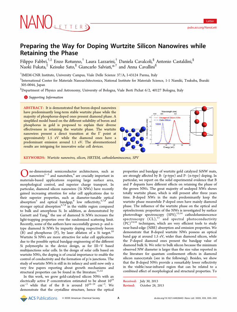
Preparing the Way for Doping Wurtzite Silicon Nanowires whileRetaining the PhaseFilippo Fabbri,†,‡ Enzo Rotunno,† Laura Lazzarini,† Daniela Cavalcoli,§ Antonio Castaldini,§
Naoki Fukata,‡ Keisuke Sato,§ Giancarlo Salviati,*,† and Anna Cavallini§
†IMEM-CNR Institute, University Campus, Viale Delle Scienze 37/A, I-43124 Parma, Italy‡International Center for Materials Nanoarchitectonics, National Institute for Materials Science, 1-1 Namiki, Tsukuba, Ibaraki305-0044, Japan§Department of Physics and Astronomy, University of Bologna, Viale Berti Pichat 6/2, 40127 Bologna, Italy
*S Supporting Information
ABSTRACT: It is demonstrated that boron-doped nanowireshave predominantly long-term stable wurtzite phase while themajority of phosphorus-doped ones present diamond phase. Asimplified model based on the different solubility of boron andphosphorus in gold is proposed to explain their diverseeffectiveness in retaining the wurtzite phase. The wurtzitenanowires present a direct transition at the Γ point atapproximately 1.5 eV while the diamond ones have apredominant emission around 1.1 eV. The aforementionedresults are intriguing for innovative solar cell devices.
KEYWORDS: Wurtzite nanowires, silicon, HRTEM, cathodoluminescence, SPV
One-dimensional semiconductor architectures, such asnanowires1−3 and nanotubes,4 are crucially important in
materials-based applications requiring large surface area,morphological control, and superior charge transport. Inparticular, diamond silicon nanowires (Si NWs) have recentlygained increasing attention for solar cell applications due totheir superior properties, such as diameter-tunable opticalabsorption5 and optical bandgap,6 low reflectivity,5,7,8 andstronger optical absorption5,7,8 in the visible region comparedto bulk and amorphous Si. In addition, as demonstrated byGarnett and Yang,9 the use of diamond Si NWs increases thelight-trapping properties over the randomized scattering limit.Recently, some of the authors have successfully grown p- and n-type diamond Si NWs by impurity doping respectively boron(B) and phosphorus (P), by laser ablation of a Si target.10
Wurtzite Si NWs are more attractive for solar cell applicationsdue to the possible optical bandgap engineering of the differentSi polymorphs in the device design, as for III−V basedmultijunctions solar cells. In the design of solar cells based onwurtzite NWs, the doping is of crucial importance to enable thecontrol of conductivity and the formation of p/n junctions. Thestudy of wurtzite NWs is still in its infancy and until now only avery few papers reporting about growth mechanisms andstructural properties can be found in the literature.11,12
In this work, we grow gold-catalyzed silicon NWs with anelectrically active P concentration estimated to be about 1019
cm−3 while that of the B is around 1018−19 cm−3. Wedemonstrate that the crystalline structure, hence the optical
properties and bandgap of wurtzite gold catalyzed SiNW mats,are strongly affected by B- (p-type) and P- (n-type) doping. Inparticular, we report on the solid experimental evidence that Band P dopants have different effects on retaining the phase ofthe grown NWs. The great majority of undoped NWs showstotally wurtzite phase, which is still present after three yearstime. B-doped NWs in the mats predominantly keep thewurtzite phase meanwhile P-doped ones have mainly diamondphase. The influence of the wurtzite phase on the optical andoptoelectronic properties of the NWs is investigated by surfacephotovoltage spectroscopy (SPS),13,14 cathodoluminescencespectroscopy (CL),15 and spectral photoconductivity(PC)14,16 techniques, which are very efficient tools to studynear-band-edge (NBE) absorption and emission properties. Wedemonstrate that B-doped wurtzite NWs possess an opticalband gap at around 1.5 eV, wider than diamond silicon, whilethe P-doped diamond ones present the bandgap value ofdiamond bulk Si. We refer to bulk silicon because the minimumobserved NW diameter is larger than the size value reported inthe literature for quantum confinement effects in diamondsilicon nanocrystals (see in the following). Besides, we showthat the B-doped NWs provide a remarkably lower reflectivityin the visible/near-infrared region that can be related to acombined effect of morphological and structural properties. To
Received: July 30, 2013Revised: October 28, 2013
Letter
pubs.acs.org/NanoLett
© XXXX American Chemical Society A dx.doi.org/10.1021/nl4028445 | Nano Lett. XXXX, XXX, XXX−XXX
the best of our knowledge, this is the first experimentalevidence of B and P doping of wurtzite silicon NWs. Ourresults prepare the way to the control of structural, optical, andtransport properties of Si nanowires in view of innovativedevice engineering.Si NWs are synthesized by means of a gold nanocluster-
catalyzed vapor−liquid−solid (VLS) growth mechanism17 in acommercial cold wall CVD system at a total pressure rangingfrom 8 to 10 Torr. The growth rate of NWs was about 300 nm/min. The substrates were thermally oxidized Si with an oxidethickness of 200 nm; Au nanocolloidal particles of 3 nm indiameter were used as metal catalyst. For B- and P-doped NWssynthesis, they are directly grown onto thermally oxidized Sisubstrates at a temperature of 600 °C for 30 min in flowing 19sccm of SiH4 as the silicon reactant gas, 1% B2H6 (0.5 sccm) inH2 as p-type dopant gas, 1% PH3 in H2 as n-type dopant gasand 30 sccm of nitrogen (N2) as the carrier gas. It is importantto remember that the growth temperature of our NWs is higherthan that reported, for example, in refs 18−21 (that was around450−460 °C), which present cubic Si NWs. In addition, alsoour precursors flow rates were different. On the contrary, ourgrowth conditions are similar to those of ref 11, which reportson hexagonal NWs. Figure 1 shows the typical nanowire mat
obtained by this procedure. The acceptor concentration in B-doped NWs is roughly estimated to be in the order of 1018−1019 cm−3 by Raman spectroscopy.10 The electrical active Pconcentration can be estimated to be about 1019 cm−3.The crystalline structure of Si NWs is determined by electron
microscopy techniques in a JEOL 2200FS field emissionmicroscope operating at 200 kV. The samples for HRTEMobservation are prepared by dropping dilute dispersion solutionof NWs onto holey-carbon grids, and their analysis is carriedout on several hundreds of NWs. The optical andoptoelectronic properties of the NWs are investigated bySPS, PC, CL, and reflectivity analyses. SPS measurements areconducted at room temperature by means of a custom-madeapparatus based on a SPEX 500 M monochromator equippedwith quartz-tungsten-halogen (QTH) lamp.22 The surfacephotovoltage (SPV) signal, capacitively picked up by asemitransparent electrode, goes through a high impedancefield effect transistor preamplifer, and is measured by a lock-inamplifer. The SPV data are normalized by the photon fluximpinging over the sample.
A commercial Gatan monoCL system, fitted onto an S360Cambridge SEM, is used for the CL spectroscopy. The systemis equipped by a grating and a Ge photodiode, sensitive in therange 700−1550 nm (1.7−0.8 eV). CL experiments areperformed at room temperature on tens of NWs after removingfrom the substrate. An accelerating voltage of 7.5 keV is chosento release homogeneous amount of energy along the NWdiameter (see Figure S10 and S13 in the SupportingInformation). The current is 115 nA. For the CL analysis ofbulk Si, the accelerating voltage is kept constant and the currentis increased up to 10 μA due to its extremely lower radiativeefficiency.The reflectance is measured at a reflection angle of 45° at
room temperature. PC measurements are carried out at roomtemperature by means of a custom-made apparatus based on aCornerStone 260 monochromator equipped with a QTH lamp.The photocurrent signal is collected through two ohmiccontacts on the NW mat by a lock-in amplifier and normalizedto the photon flux. The ohmic contacts are prepared byevaporating a 300 nm thick gold onto the NW mats. Theschematic of the sample and contacts for PC measurements isreported in Figure S14 in the Supporting Information.It is worth noting that, apart for the HRTEM observations,
the results obtained come from the majority of the NWs in themats, representing the behavior of wurtzite NWs in B-dopedsamples and the behavior of the diamond NWs in P-dopedsamples.The structural characterization is obtained by comparing
high-resolution transmission electron microscopy (HRTEM)and electron diffraction on hundreds of NWs for different wireorientation. The TEM investigations show that the undoped,the B- and P-doped NWs can crystallize in the wurtzite ordiamond phases and the two different polymorphs never occurin the same NW. From the TEM analyses, we found that thedoping species have a completely different effect on thecrystalline properties of the NWs, thereby causing the variationof the relative abundance of two polymorphs. The onset of thesmall percentage of the diamond phase in B-doped NWscompared to the undoped ones is probably related to the stressrelease caused by the formation of planar defects, that is, twinplanes (see Figure S2 in the Supporting Information).All the NWs studied in this work are single crystals either
wurtzite or diamond in nature. In these monocrystalline NWs,we do not observe any other of the possible hexagonalpolymorphs intermediate between the diamond and thewurtzite structures (see, for example, ref 23). Moreover,according to the classification of Fontcuberta i Morral et al.11
we mainly observe the type A wurtzite structure with a = 0.38nm and c = 0.627 nm and only occasionally the type B one witha = 0. 404 nm and c = 0.660 nm. The WZ phase is alsoconfirmed by X-ray diffraction studies performed on boron-doped samples (see Supporting Information for a deepdiscussion of this argument and Figures S2−S5).The type A phase is precisely determined by high-resolution
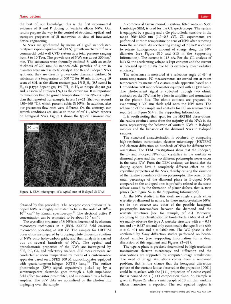
transmission electron microscopy and diffraction and theobservations are supported by computer image simulations.The need of image simulations comes from a renownedproblem, that is, the chance that the hexagonal diffractionpattern of the wurtzite lattice observed in the projection [0001]could be mistaken with the [111] projection of a cubic crystalthat is twinned on a (111) composition plane. An example isgiven in Figure 2a where a micrograph of 10 nm thin wurtzitesilicon nanowires is reported. The red squared region is
Figure 1. SEM micrograph of a typical mat of B-doped Si NWs.
Nano Letters Letter
dx.doi.org/10.1021/nl4028445 | Nano Lett. XXXX, XXX, XXX−XXXB
enlarged in Figure 2b and is compared with the computerimage simulations24 of the wurtzite silicon and the cubictwinned silicon, respectively, shown in Figure 2c,d, obtained inthe same experimental conditions of Figure 2b. It is apparentthat there is no possibility of mistaking the two structures. Ourexperimental image is exactly reproduced by the WZ structuresimulation with lattice periodicity d10−10 = 0.33 nm. The sameperiodicity is also present in the image simulation of thetwinned crystal but only as an extra periodicity, being theinterplanar distance d110 of the diamond silicon equal to 0.192nm. The detailed explanation can be found in the Figures S1−S4 in the Supporting Information.In the literature, the lattice periodicity of 0.33 nm has also
been observed in very thin diamond Si nanowires (see, forexample, refs 18−21) where it has been attributed to theforbidden 1/3 ⟨422⟩ reflections following.25,26
The explanation to justify the presence of the forbiddenfractional reflections of the type 1/3 ⟨422⟩ cannot be applied toour case for two main reasons:(1) According to ref 25 the possibility to see such reflections
is limited to “exceptionally thin and flat” samples (t < 30 nm asin the case of refs 18−21). As already mentioned and as shownin Supporting Information Figure S5, we observed thosereflections in wires with diameters up to 260 nm and not so flat.(2) The papers that deal with these forbidden reflections
(see ref 26 and references therein) insist that they are weak; onthe contrary, we always find that they are at least as intense asthe common [220] reflections, but in some cases they are moreintense, as it can be seen in Supporting Information Figure S5.From the TEM analyses we found that the doping species
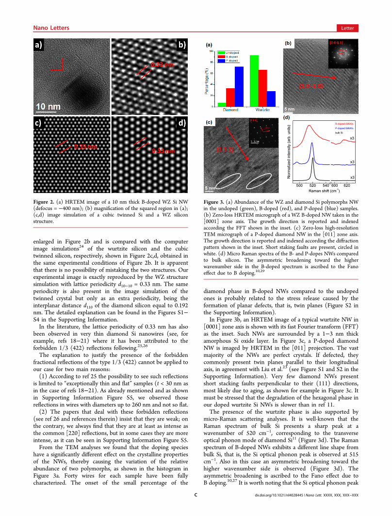
have a significantly different effect on the crystalline propertiesof the NWs, thereby causing the variation of the relativeabundance of two polymorphs, as shown in the histogram inFigure 3a. Forty wires for each sample have been fullycharacterized. The onset of the small percentage of the
diamond phase in B-doped NWs compared to the undopedones is probably related to the stress release caused by theformation of planar defects, that is, twin planes (Figure S2 inthe Supporting Information).In Figure 3b, an HRTEM image of a typical wurtzite NW in
[0001] zone axis is shown with its fast Fourier transform (FFT)as the inset. Such NWs are surrounded by a 1−3 nm thickamorphous Si oxide layer. In Figure 3c, a P-doped diamondNW is imaged by HRTEM in the [011] projection. The vastmajority of the NWs are perfect crystals. If defected, theycommonly present twin planes parallel to their longitudinalaxis, in agreement with Liu et al.23 (see Figure S1 and S2 in theSupporting Information). Very few diamond NWs presentshort stacking faults perpendicular to their (111) directions,most likely due to aging, as shown for example in Figure 3c. Itmust be stressed that the degradation of the hexagonal phase inour doped wurtzite Si NWs is slower than in ref 11.The presence of the wurtzite phase is also supported by
micro-Raman scattering analyses. It is well-known that theRaman spectrum of bulk Si presents a sharp peak at awavenumber of 520 cm−1, corresponding to the transverseoptical phonon mode of diamond Si11 (Figure 3d). The Ramanspectrum of B-doped NWs exhibits a different line shape frombulk Si, that is, the Si optical phonon peak is observed at 515cm−1. Also in this case an asymmetric broadening toward thehigher wavenumber side is observed (Figure 3d). Theasymmetric broadening is ascribed to the Fano effect due toB doping.10,27 It is worth noting that the Si optical phonon peak
Figure 2. (a) HRTEM image of a 10 nm thick B-doped WZ Si NW(defocus = −400 nm); (b) magnification of the squared region in (a);(c,d) image simulation of a cubic twinned Si and a WZ siliconstructure.
Figure 3. (a) Abundance of the WZ and diamond Si polymorphs NWin the undoped (green), B-doped (red), and P-doped (blue) samples.(b) Zero-loss HRTEM micrograph of a WZ B-doped NW taken in the[0001] zone axis. The growth direction is reported and indexedaccording the FFT shown in the inset. (c) Zero-loss high-resolutionTEM micrograph of a P-doped diamond NW in the [011] zone axis.The growth direction is reported and indexed according the diffractionpattern shown in the inset. Short staking faults are present, circled inwhite. (d) Micro Raman spectra of the B- and P-dopes NWs comparedto bulk silicon. The asymmetric broadening toward the higherwavenumber side in the B-doped spectrum is ascribed to the Fanoeffect due to B doping.10,29
Nano Letters Letter
dx.doi.org/10.1021/nl4028445 | Nano Lett. XXXX, XXX, XXX−XXXC
is too largely downshifted with respect to the cubic siliconoptical phonon, even taking into account the impact of dopingand phonon confinement effects28 of the NWs tip.In P-doped NWs, the Si optical phonon (TO) peak is set at
519 cm−1 with an asymmetric broadening toward the lowerwavenumber side. The downshift and the broadening of TOpeak can be ascribed to doping and phonon confinementeffects28 and to the possible convolution with other peaks. Anadditional peak at 495 cm−1 also appears. Previous works29−31
report on two main TO peaks around 495 and 517 cm−1 thatthe authors assign to the hexagonal phase of Si. On the otherhand, ref 11 shows a peak at 503 cm−1 that is also ascribed tohexagonal Si. Our TO peaks around 495 and 519 cm−1 aremore in agreement with refs 30 and 31 rather than with ref 11.We ascribe the small shift from 517 to 519 cm−1 to thepresence of 70% of cubic phase in the P-doped NWs that givesrise to a TO peak at 520 cm−1.Therefore, we conclude that the peak at 515 cm−1 observed
from B-doped NWs is due to the wurtzite silicon phase.29−31
The asymmetric broadening of the Si optical phonon peakrelated to the Fano effect masks the 495 cm−1 peak (to supportour findings the Raman spectrum of the undoped NWs is alsoreported in Figure S7 in the Supporting Information).Additionally, B-doped NWs present a further peak at about618 cm−1, due to the B local vibrational mode.10 The detectionof the B local vibrational mode and Fano broadening is thedirect evidence that B atoms are located in substitutional sitesof the silicon lattice and are electrically active. This analysisfurther supports the presence of different dominating phases inthe samples doped with different atomic species, consistentlywith the observations made by HRTEM statistics.In order to determine the optical bandgap of Si NWs, their
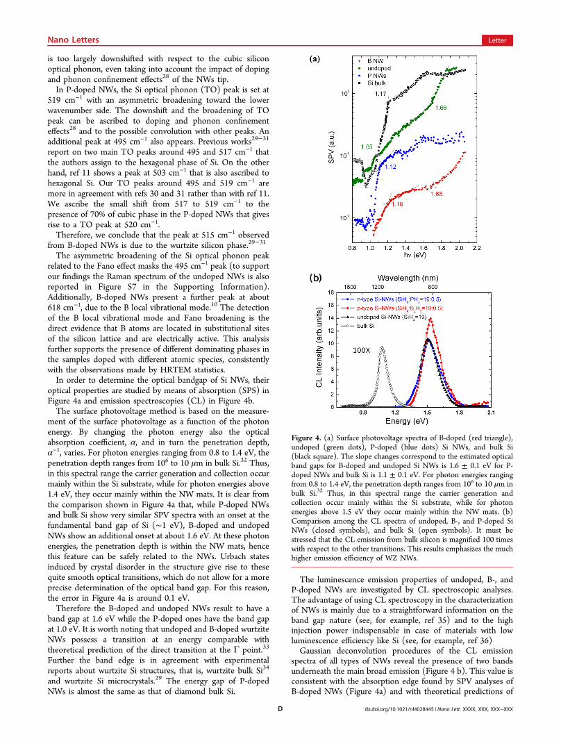
optical properties are studied by means of absorption (SPS) inFigure 4a and emission spectroscopies (CL) in Figure 4b.The surface photovoltage method is based on the measure-
ment of the surface photovoltage as a function of the photonenergy. By changing the photon energy also the opticalabsorption coefficient, α, and in turn the penetration depth,α−1, varies. For photon energies ranging from 0.8 to 1.4 eV, thepenetration depth ranges from 106 to 10 μm in bulk Si.32 Thus,in this spectral range the carrier generation and collection occurmainly within the Si substrate, while for photon energies above1.4 eV, they occur mainly within the NW mats. It is clear fromthe comparison shown in Figure 4a that, while P-doped NWsand bulk Si show very similar SPV spectra with an onset at thefundamental band gap of Si (∼1 eV), B-doped and undopedNWs show an additional onset at about 1.6 eV. At these photonenergies, the penetration depth is within the NW mats, hencethis feature can be safely related to the NWs. Urbach statesinduced by crystal disorder in the structure give rise to thesequite smooth optical transitions, which do not allow for a moreprecise determination of the optical band gap. For this reason,the error in Figure 4a is around 0.1 eV.Therefore the B-doped and undoped NWs result to have a
band gap at 1.6 eV while the P-doped ones have the band gapat 1.0 eV. It is worth noting that undoped and B-doped wurtziteNWs possess a transition at an energy comparable withtheoretical prediction of the direct transition at the Γ point.33
Further the band edge is in agreement with experimentalreports about wurtzite Si structures, that is, wurtzite bulk Si34
and wurtzite Si microcrystals.29 The energy gap of P-dopedNWs is almost the same as that of diamond bulk Si.
The luminescence emission properties of undoped, B-, andP-doped NWs are investigated by CL spectroscopic analyses.The advantage of using CL spectroscopy in the characterizationof NWs is mainly due to a straightforward information on theband gap nature (see, for example, ref 35) and to the highinjection power indispensable in case of materials with lowluminescence efficiency like Si (see, for example, ref 36)Gaussian deconvolution procedures of the CL emission
spectra of all types of NWs reveal the presence of two bandsunderneath the main broad emission (Figure 4 b). This value isconsistent with the absorption edge found by SPV analyses ofB-doped NWs (Figure 4a) and with theoretical predictions of
Figure 4. (a) Surface photovoltage spectra of B-doped (red triangle),undoped (green dots), P-doped (blue dots) Si NWs, and bulk Si(black square). The slope changes correspond to the estimated opticalband gaps for B-doped and undoped Si NWs is 1.6 ± 0.1 eV for P-doped NWs and bulk Si is 1.1 ± 0.1 eV. For photon energies rangingfrom 0.8 to 1.4 eV, the penetration depth ranges from 106 to 10 μm inbulk Si.32 Thus, in this spectral range the carrier generation andcollection occur mainly within the Si substrate, while for photonenergies above 1.5 eV they occur mainly within the NW mats. (b)Comparison among the CL spectra of undoped, B-, and P-doped SiNWs (closed symbols), and bulk Si (open symbols). It must bestressed that the CL emission from bulk silicon is magnified 100 timeswith respect to the other transitions. This results emphasizes the muchhigher emission efficiency of WZ NWs.
Nano Letters Letter
dx.doi.org/10.1021/nl4028445 | Nano Lett. XXXX, XXX, XXX−XXXD
the direct transition at the Γ point of wurzite silicon.33 Bycomparing the CL integrated intensities of the 1.53 eV peak forall the NWs, the B-doped NWs intensity results stronger thanthose of the undoped and P-doped ones. The undoped NWshave almost the great majority of wurtzite phase but have thesame CL integrated intensity of the P-doped ones; further, theNW densities we measured are 8 × 10⁸ and 1012 cm−2 for B-doped and P-doped mats, respectively. From these observa-tions, it follows that the more intense CL emission of the B-doped samples can only be due to their larger diameter (seeFigure S11 and S12 in the Supporting Information) withrespect to the undoped and P-doped NWs. Actually, as shownfrom Monte Carlo simulations (Figure S10 in the SupportingInformation), the shape and dimension of the generation-recombination volume and the CL efficiency depend on theNW diameter. As a consequence, larger NWs give higher CLintegrated intensity .The diameters of B-doped NWs exhibit a broad, Gaussian-
like, distribution, ranging from 100 to 530 nm. Their meanvalue is 380 nm with a standard error of ±50 nm. Differently,the diameters of the P-doped NWs exhibit a stronglyasymmetric distribution with a sharp peak followed by a longtail, where the diameters range from about 15−160 nm. Theirmean diameter is 26 nm with a standard error of ±9 nm.Considering the diameter statistics of all types of NWs, no
quantum confinement effect can be expected37 (see Figure S12in the Supporting Information). The CL band around 1.68 eVis ascribed to SiOx-related luminescence centers, as reported byref 38 or to amorphous silicon.39 This hypothesis is alsosupported by our HRTEM observations that show the presenceof a few nanometers-thick SiOx outer layer on all types of NWcore (Figure 1a, and Figure S1 in the Supporting Information).Assuming a Stokes shift of 60 meV,40 we ascribe the CLemission band at 1.06 eV to the NBE transition of thediamond-like structure of bulk Si (Figure 4b). It is worth notingthat in order to obtain the CL emission intensity by the bulk Sicomparable with the NWs one, an injection power 2 orders ofmagnitude higher must be used. Therefore, after renormalizingall the integrated intensities to the injection power, the resultsare (in arbitrary units) 2750, 2786, 3195, and 15 for undoped,P-, and B-doped NWs, and bulk Si, respectively. This findingdemonstrates that wurtzite NWs possess a radiative efficiency 2orders of magnitude higher than cubic bulk Si.Quantum efficiency analyses are carried out (see Figure S8 in
the Supporting Information) to clarify the effect of the wurtzitestructure on the optoelectronic behaviors of electrically activeSi NWs.Reflectivity studies are also performed on both types of
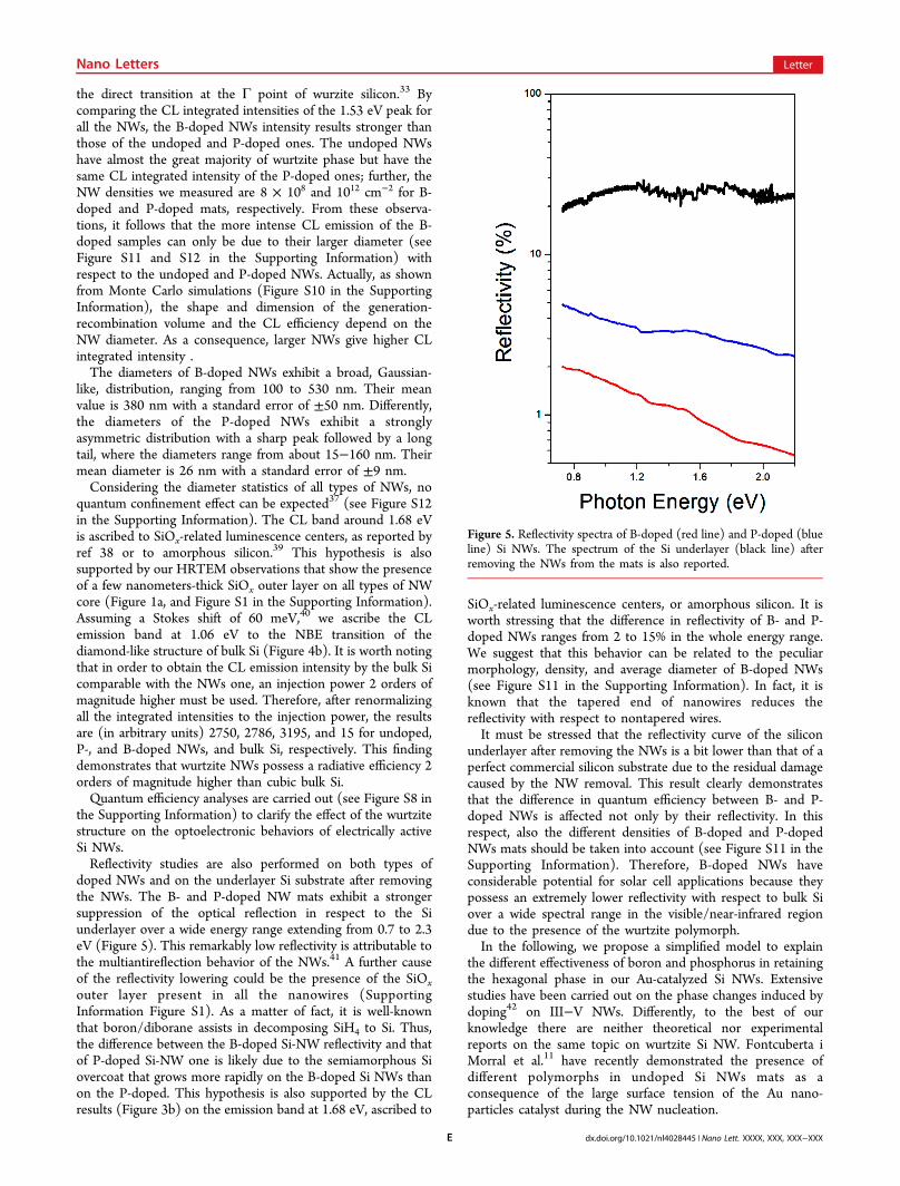
doped NWs and on the underlayer Si substrate after removingthe NWs. The B- and P-doped NW mats exhibit a strongersuppression of the optical reflection in respect to the Siunderlayer over a wide energy range extending from 0.7 to 2.3eV (Figure 5). This remarkably low reflectivity is attributable tothe multiantireflection behavior of the NWs.41 A further causeof the reflectivity lowering could be the presence of the SiOxouter layer present in all the nanowires (SupportingInformation Figure S1). As a matter of fact, it is well-knownthat boron/diborane assists in decomposing SiH4 to Si. Thus,the difference between the B-doped Si-NW reflectivity and thatof P-doped Si-NW one is likely due to the semiamorphous Siovercoat that grows more rapidly on the B-doped Si NWs thanon the P-doped. This hypothesis is also supported by the CLresults (Figure 3b) on the emission band at 1.68 eV, ascribed to
SiOx-related luminescence centers, or amorphous silicon. It isworth stressing that the difference in reflectivity of B- and P-doped NWs ranges from 2 to 15% in the whole energy range.We suggest that this behavior can be related to the peculiarmorphology, density, and average diameter of B-doped NWs(see Figure S11 in the Supporting Information). In fact, it isknown that the tapered end of nanowires reduces thereflectivity with respect to nontapered wires.It must be stressed that the reflectivity curve of the silicon
underlayer after removing the NWs is a bit lower than that of aperfect commercial silicon substrate due to the residual damagecaused by the NW removal. This result clearly demonstratesthat the difference in quantum efficiency between B- and P-doped NWs is affected not only by their reflectivity. In thisrespect, also the different densities of B-doped and P-dopedNWs mats should be taken into account (see Figure S11 in theSupporting Information). Therefore, B-doped NWs haveconsiderable potential for solar cell applications because theypossess an extremely lower reflectivity with respect to bulk Siover a wide spectral range in the visible/near-infrared regiondue to the presence of the wurtzite polymorph.In the following, we propose a simplified model to explain
the different effectiveness of boron and phosphorus in retainingthe hexagonal phase in our Au-catalyzed Si NWs. Extensivestudies have been carried out on the phase changes induced bydoping42 on III−V NWs. Differently, to the best of ourknowledge there are neither theoretical nor experimentalreports on the same topic on wurtzite Si NW. Fontcuberta iMorral et al.11 have recently demonstrated the presence ofdifferent polymorphs in undoped Si NWs mats as aconsequence of the large surface tension of the Au nano-particles catalyst during the NW nucleation.
Figure 5. Reflectivity spectra of B-doped (red line) and P-doped (blueline) Si NWs. The spectrum of the Si underlayer (black line) afterremoving the NWs from the mats is also reported.
Nano Letters Letter
dx.doi.org/10.1021/nl4028445 | Nano Lett. XXXX, XXX, XXX−XXXE
It is known that boron and phosphorus have differentsolubilities in gold with boron keeping the lowest (see refs 43and 44 where it is reported that the solubility of boron in goldis lower than 5%). Therefore, most likely during the growth ofour gold-catalyzed NWs, the surface tension of the Aunanoparticle is not affected by the presence of boron thusresulting in a growth mechanism similar to that of undopedwurzite Si NWs that predominantly are present in the wurtzitephase (Figure 2a). On the contrary, phosphorus has a solubilityin gold of 13%45 and therefore the surface tension of the goldcatalyst NP can be strongly modified by phosphorus thusinducing a different growth mechanism giving rise to thenucleation of a significant amount of diamond nanowires.Since this is the first experimental report on the influence of
doping in retaining the hexagonal phase of wurtzite siliconNWs and because of the lack of any models in the literature onthis topic, alternative explanations can be adopted forexplaining our findings. For instance, the possibility that athigh growth rates the P or B may change the growth kineticsleading to one phase or the other being more favorablystabilized could be taken into account. However, to the best ofour knowledge it is not possible to discriminate among thedifferent explanations without experimentally defining theternary phase diagrams involving silicon, gold, and dopantatoms that are not presently available in the literature. That ishowever beyond the purpose of the present work.In this study, we prepare the way for p- and n-type doping
silicon nanowires while retaining their wurtzite phase. HRTEMstudies demonstrate that boron- and phosphorus-doped NWs,respectively, keep about 67 and 28% of wurtzite phase in themats with the two polymorphs never coexisting in the sameNW. Our optical investigations also prove that wurtzitenanowires present a direct transition at the Γ point around1.5 eV. On the contrary, the emission of diamond nanowiresoccurs approximately at 1.1 eV. Moreover, a remarkably lowerreflectivity in the range from 0.7 to 2.2 eV is reported for B-doped Si NWs mats, reasonably due to both structural andmorphological features.Therefore, we strongly believe that B-doped wurtzite NWs
have considerable potential for solar cell applications due to thedirect transition and to a low reflectivity.
■ ASSOCIATED CONTENT
*S Supporting InformationTEM image of a defected cubic wire on the B-doped sample,atomic model of the two structure that could be confusedduring the TEM observations, HRTEM simulations of thepossible structures at different defocus, XRD analysis of B-doped NWs, Raman analyses of the undoped Si-NWs mat,quantum efficiency of P-doped NWs mats and siliconunderlayer, Gaussian deconvolutions of the CL spectra,Monte Carlo simulation for the generation-recombinationvolume, morphological analyses of the samples, BF-TEMimage showing the tapering of the B-doped NWs, threedimensional map of the energy released along the diameter ofSi-NWs, schematic for the PCS characterization. This materialis available free of charge via the Internet at http://pubs.acs.org.
■ AUTHOR INFORMATION
Corresponding Author*E-mail: [email protected].
NotesThe authors declare no competing financial interest.
■ ACKNOWLEDGMENTSN.F. was supported by a Funding Program for Next GenerationWorld-Leading Researchers (NEXT Program) in Japan. Theresearch has been partly supported by the Italian-JapaneseProgetto di Grande Rilevanza “Nanoscale assEssMent ofchEmical and phySical propertIes of advanced nanoStructures(NEMESIS)“ funded by the Italian Ministry of Foreign Affairs.Thanks are due to Prof. G. Calestani for X-ray investigations.
■ REFERENCES(1) Novotny, C. J.; Yu, E. T.; Yu, P. K. L. Nano Lett. 2008, 8, 775−779.(2) Lu, S.; Lingley, Z.; Asano, T.; Harris, D.; Barwicz, T.; Guha, S.;Madhukar, A. Nano Lett. 2009, 9, 4548−4552.(3) Ren, S.; Zhao, N.; Crawford, S. C.; Tambe, M.; Bulovic, V.;Gradecak, S. Nano Lett. 2011, 11, 408−413.(4) Shu, Q.; Wei, J.; Wang, K.; Zhu, H.; Li, Z.; Jia, Y.; Gui, X.; Guo,N.; Li, X.; Ma, C.; Wu, D. Nano Lett. 2009, 9, 4338−4342.(5) Adachi, M. M.; Anantram, M. P.; Karim, K. S. Nano Lett. 2010,10, 4093−4098.(6) Nolan, M.; O’Callaghan, S.; Fagas, G.; Greer, J. C. Nano Lett.2007, 7, 34−38.(7) Tsakalakos, L.; Balch, J.; Fronheiser, J.; Shih, M.-Y.; LeBoeuf, S.F.; Pietrzykowski, M.; Codella, P. J.; Korevaar, B. A.; Sulima, O.; Rand,J.; Davuluru, A.; Rapol, U. J. Nanophotonics 2007, 1, 013552.(8) Sivakov, V.; Andra, G.; Gawlik, A.; Berger, A.; Plentz, J.; Falk, F.;Christiansen, S. H. Nano Lett. 2009, 9, 1549−1554.(9) Garnett, E.; Yang, P. Nano Lett. 2010, 10, 1082−1087.(10) Fukata, N.; Ishida, S.; Yokono, S.; Takiguchi, R.; Chen, J.;Sekiguchi, T.; Murakami, K. Nano Lett. 2011, 11, 651−656.(11) Fontcuberta i Morral, A.; Arbiol, J.; Prades, J. D.; Cirera, A.;Morante, J. R. Adv. Mater. 2007, 19, 1347−1351.(12) Li, F.; Nellist, P. D.; Lang, C.; Cockayne, D. J. H. J. Phys.: Conf.Ser. 2010, 241, 012088.(13) Kronik, L.; Shapira, Y. Surf. Interface Anal. 2001, 31, 954−965.(14) Cavallini, A.; Polenta, L.; Rossi, M.; Stoica, T.; Calarco, R.;Meijers, R. J.; Richter, T.; Luth, H. Nano Lett. 2007, 7, 2166−2170.(15) Fabbri, F.; Rossi, F.; Attolini, G.; Salviati, G.; Iannotta, S.;Aversa, L.; Verucchi, R.; Nardi, M.; Fukata, N.; Dierre, B.; Sekiguchi,T. Nanotechnology 2010, 21, 345702.(16) Bube, R. H. Photoconductivity of solids; Wiley: New York, 1960.(17) Wagner, R. S.; Ellis, W. C. Appl. Phys. Lett. 1964, 4, 89−90.(18) Tian, B.; Xie, P.; Kempa, T. J.; Bell, D. C.; Lieber, C. M. Nat.Nanotechnol. 2009, 4, 824−829.(19) Tian, B.; Zheng, X.; Kempa, T. J.; Fang, Y.; Yu, N.; Yu, G.;Huang, J.; Lieber, C. M. Nature 2007, 449, 885−890.(20) Wu, Y.; Cui, Y.; Huynh, L.; Barrelet, C. J.; Bell, D. C.; Lieber, C.M. Nano Lett. 2004, Vol. 4 (No. 3), 433−436.(21) Cui, Y.; Lauhon, L. J.; Gudiksen, M. S.; Wang, J.; Lieber, C. M.Appl. Phys. Lett. 2001, 78, 2214−2216.(22) Castaldini, A.; Cavalcoli, D.; Cavallini, A.; Rossi, M. Sol. EnergyMater. Sol. Cells 2002, 72, 559−569.(23) Liu, X.; Wang, D. Nano Res. 2009, 2, 575−582.(24) Grillo, V.; Rotunno, E. Ultramicroscopy 2013, 125, 97−111.(25) Ourmadz, B. A.; Anstis, G. R.; Hirsch, P. B. Philos. Mag. A 1983,48, 139−153.(26) Gibson, J. M.; Lanzerott, M. Y.; Elser, V. Appl. Phys. Lett. 1989,55 (13), 1394−1396.(27) Fano, U. Phys. Rev. 1961, 124, 1866−1878.(28) Fukata, N.; Oshima, T.; Murakami, K.; Kizuka, T.; Tsurui, T.;Ito, S. Appl. Phys. Lett. 2005, 86, 213112.(29) Bandet, J.; Despax, B.; Caumont, M. J. Phys. D: Appl. Phys. 2002,35, 234−239.(30) Lopez, F. J.; Givan, U.; Connell, J. G.; Lauhon, L. J. ACS Nano2011, 5, 8958−8966.
Nano Letters Letter
dx.doi.org/10.1021/nl4028445 | Nano Lett. XXXX, XXX, XXX−XXXF
(31) Lopez, F. J.; Hemesath, E. R.; Lauhon, L. J. Nano Lett. 2009, 9,2774−2779.(32) Dash, W. C.; Newman, R. Phys. Rev. 1955, 99, 1151−1155.(33) Joannopoulos, J. D.; Cohen, M. L. Phys. Rev. B 1973, 7, 2644−2657.(34) Besson, J. M.; Mokhtari, E. H.; Gonzalez, J.; Weill, G. Phys. Rev.Lett. 1987, 59, 4.(35) Lazzarini, L.; Salviati, G.; Fabbri, F.; Zha, M.; Calestani, D.;Zappettini, A.; Sekiguchi, T.; Dierre, B. ACS Nano 2009, 3, 3158−3164.(36) Fabbri, F.; Smith, M. J.; Recht, D.; Aziz, M. J.; Gradecak, S.;Salviati, G. Appl. Phys. Lett. 2013, 102, 031909−031911.(37) Beard, M. C.; Knutsen, K. P.; Yu, P.; Luther, J. M.; Song, Q.;Metzger, W. K.; Ellingson, R. J.; Nozik, A. J. Nano Lett. 2007, 7, 2506−2512.(38) Qin, G. G.; Song, H. Z.; Zhang, B. R.; Lin, J.; Duan, J. Q.; Yao,G. Q. Phys. Rev. B 1996, 54, 2548−2555.(39) Tong, S.; Liu, X.-n.; Bao, X.-m Appl. Phys. Lett. 1995, 66, 469−471.(40) Sychugov, I.; Juhasz, R.; Valenta, J.; Linnros, J. Phys. Rev. Lett.2005, 94, 087405.(41) Peng, K.; Wang, X.; Lee, S.-T. Appl. Phys. Lett. 2008, 92,163103.(42) Algra, R. E.; Verheijen, M. A.; Borgstrom, M. T.; Feiner, L.;Immink, G.; van Enckevort, W. J. P.; Vlieg, E.; Bakkers, E. P. A. M.Nature 2008, 456, 369.(43) Li, Z.; Baca, J.; Wu, J. Appl. Phys. Lett. 2008, 92, 113104.(44) Wald, F.; Stormont, R. W. J. Less-Common Met. 1965, 9, 423.(45) Okamoto, H.; Massalski, T. B. J. Phase Equilib. 1984, 5, 490.
Nano Letters Letter
dx.doi.org/10.1021/nl4028445 | Nano Lett. XXXX, XXX, XXX−XXXG
Copyright © 2022 FDOKUMEN