Polychromatic X-ray Micro and Nano-Beam Science and Instrumentation
6
Polychromatic X-ray Micro- and Nano-Beam Science and Instrumentation G.E. Ice 1 , B.C. Larson 1 , W. Liu 1 , R.I. Barabash 1 , E.D. Specht 1 , J.W.L. Pang 1 , J.D. Budai 1 ,J.Z. Tischler 1 , A. Khounsary 2 , C. Liu 2 , A.T. Macrander 2 and L. Assoufid 2 1 Materials Science and Technology Division, Oak Ridge National Laboratory, Oak Ridge TN 37831-6118 USA 2 Advanced Photon Source, Argonne National Laboratory, 9700 S. Cass Ave. Argonne Il 60439 Abstract. Polychromatic x-ray micro- and nano-beam diffraction is an emerging nondestructive tool for the study of local crystalline structure and defect distributions. Both long-standing fundamental materials science issues, and technologically important questions about specific materials systems can be uniquely addressed. Spatial resolution is determined by the beam size at the sample and by a knife-edge technique called differential aperture microscopy that decodes the origin of scattering from along the penetrating x-ray beam. First-generation instrumentation on station 34-ID- E at the Advanced Photon Source (APS) allows for nondestructive automated recovery of the three-dimensional (3D) local crystal phase and orientation. Also recovered are the local elastic-strain and the dislocation tensor distributions. New instrumentation now under development will further extend the applications of polychromatic microdiffraction and will revolutionize materials characterization. Keywords: X-ray, microbeam, nanobeam, focusing, diffraction, PACS: 61.10.Nz, 61.72.Dd INTRODUCTION AND THEORY Polychromatic microdiffraction[1] is a rapidly emerging approach to the study of mesoscale materials structure and defect distributions. This approach uses the oldest x-ray diffraction method, Laue diffraction[2], to nondestructively determine local distributions of crystal structure, orientation, elastic deviatoric strain, and dislocation tensors. This information can be mapped with submicron 3D resolution because the diffraction information is determined without the complication of sample rotations. Although the science possible with the world’s only 3D X-ray crystal microscope (station 34-ID-E at the APS) is already compelling[3], new instrumentation and technical developments will enable important new applications and will vastly accelerate data collection, analysis and interpretation. In this paper, we briefly survey the current state of the art with respect to instrumentation and science, discuss new instrumentation currently under construction, and speculate on future directions for polychromatic microdiffraction. Why Use Polychromatic Beams? The principle motivation for polychromatic microdiffraction is the ability to characterize crystal structure without sample rotations. Max Von Laue first proposed that X-rays could be used to study the atomic structural of materials in 1912. For his work Laue was awarded the Nobel prize in 1914, just 2 years later[2]. As envisioned by Laue, when a collimated polychromatic beam of x-rays impinges on a crystalline lattice, the real-space lattice efficiently reflects x-rays when the scattering from individual atoms constructively interfere at special wavelengths. The wavelengths for constructive interference depend on the lattice and its orientation to the incident beam. This condition is now called the Bragg condition and is conveniently represented by a “so called” Ewald Sphere diagram[4] (Fig. 1). An Ewald sphere diagram generalized for multiple wavelengths is illustrated in Fig. 1. The real-space crystal lattice has associated with it a reciprocal-space lattice that orients with the real space lattice. For a given wavelength 1299 Downloaded 21 Aug 2007 to 160.91.159.140. Redistribution subject to AIP license or copyright, see http://proceedings.aip.org/proceedings/cpcr.jsp
-
Upload
independent -
Category
Documents
-
view
4 -
download
0
Transcript of Polychromatic X-ray Micro and Nano-Beam Science and Instrumentation

Polychromatic X-ray Micro- and Nano-Beam Science and Instrumentation
G.E. Ice1, B.C. Larson1, W. Liu1, R.I. Barabash1, E.D. Specht1, J.W.L. Pang1, J.D. Budai1 ,J.Z. Tischler1, A. Khounsary2, C. Liu2, A.T. Macrander2 and L. Assoufid2
1Materials Science and Technology Division, Oak Ridge National Laboratory, Oak Ridge TN 37831-6118 USA 2Advanced Photon Source, Argonne National Laboratory, 9700 S. Cass Ave. Argonne Il 60439
Abstract. Polychromatic x-ray micro- and nano-beam diffraction is an emerging nondestructive tool for the study of local crystalline structure and defect distributions. Both long-standing fundamental materials science issues, and technologically important questions about specific materials systems can be uniquely addressed. Spatial resolution is determined by the beam size at the sample and by a knife-edge technique called differential aperture microscopy that decodes the origin of scattering from along the penetrating x-ray beam. First-generation instrumentation on station 34-ID-E at the Advanced Photon Source (APS) allows for nondestructive automated recovery of the three-dimensional (3D) local crystal phase and orientation. Also recovered are the local elastic-strain and the dislocation tensor distributions. New instrumentation now under development will further extend the applications of polychromatic microdiffraction and will revolutionize materials characterization.
Keywords: X-ray, microbeam, nanobeam, focusing, diffraction, PACS: 61.10.Nz, 61.72.Dd
INTRODUCTION AND THEORY
Polychromatic microdiffraction[1] is a rapidly emerging approach to the study of mesoscale materials structure and defect distributions. This approach uses the oldest x-ray diffraction method, Laue diffraction[2], to nondestructively determine local distributions of crystal structure, orientation, elastic deviatoric strain, and dislocation tensors. This information can be mapped with submicron 3D resolution because the diffraction information is determined without the complication of sample rotations. Although the science possible with the world’s only 3D X-ray crystal microscope (station 34-ID-E at the APS) is already compelling[3], new instrumentation and technical developments will enable important new applications and will vastly accelerate data collection, analysis and interpretation. In this paper, we briefly survey the current state of the art with respect to instrumentation and science, discuss new instrumentation currently under construction, and speculate on future directions for polychromatic microdiffraction.
Why Use Polychromatic Beams?
The principle motivation for polychromatic microdiffraction is the ability to characterize crystal structure without
sample rotations. Max Von Laue first proposed that X-rays could be used to study the atomic structural of materials in 1912. For his work Laue was awarded the Nobel prize in 1914, just 2 years later[2]. As envisioned by Laue, when a collimated polychromatic beam of x-rays impinges on a crystalline lattice, the real-space lattice efficiently reflects x-rays when the scattering from individual atoms constructively interfere at special wavelengths. The wavelengths for constructive interference depend on the lattice and its orientation to the incident beam. This condition is now called the Bragg condition and is conveniently represented by a “so called” Ewald Sphere diagram[4] (Fig. 1).
An Ewald sphere diagram generalized for multiple wavelengths is illustrated in Fig. 1. The real-space crystal lattice has associated with it a reciprocal-space lattice that orients with the real space lattice. For a given wavelength
1299
Downloaded 21 Aug 2007 to 160.91.159.140. Redistribution subject to AIP license or copyright, see http://proceedings.aip.org/proceedings/cpcr.jsp

FIGURE 1. Ewald spheres for high energy (large diameter) and low energy (small diameter) limits of a polychromatic x-ray beam. Reciprocal lattice points which lie within the volume defined by the low and high energy limits represent Laue spots (Bragg reflections) excited by the incident beam.
FIGURE 2. Three ways to keep the exit beam coincident with a polychromatic beam: a. Heat one crystal to compensate for the small angular divergence of the straight-through and monochromatized beams; b. a four-crystal monochromator; c. compensate for the slight angular divergence with an upstream pair of mirrors.
(for example the green sphere) the Ewald Sphere indicates the possible momentum transfers for elastic scattering. If the Ewald sphere intercepts one of the reciprocal space lattice points, then a Bragg (or Laue) reflection occurs. With monochromatic diffraction the orientation of the sample is adjusted to pass reciprocal lattice points through the Ewald Sphere. With Laue diffraction a broad bandpass beam is directed at the sample. As shown in Fig. 1, a broad-bandpass beam ensures that a volume of reciprocal space is sampled without sample rotations. Any lattice point between the maximum and minimum Ewald spere surfaces is efficiently diffracted. This makes it relatively straightforward to determine the local crystal structure and sample orientation.
The number of reciprocal space points, nr, that can be detected, depends on the unit cell size a0, the symmetry of the unit cell, the solid angle subtended by the area detector, Ω, the characteristic wavelength, λ, of the x-ray beam and the bandpass of the radiation Δλ [5]. For a FCC alloy with the detector centered at 90 degrees to the incident beam, the approximate number of reflections from a crystal is,
nr =a0
3Ω
4λ3Δλλ
⎛ ⎝ ⎜
⎞ ⎠ ⎟ (1)
For a simple FCC metal with a0~3.5Å, with λ~0.8 Å, with Δλ/λ~ 0.4 and with a detector solid angle of ~1 steradians we expect about 8 reflections. More reflections are detected for larger unit cell size, higher x-ray energy, broader bandpass, or larger solid angle.
Formally a Laue pattern is made up of radial line integrals through reciprocal space weighted by the spectral distribution of the incident beam and the structure factor of the sample volume [6]. This description of Laue diffraction is only realized in the ideal case where the x-ray beam impinges on a large single crystal. In real materials, x-ray beams penetrate through regions with inhomogeneous crystalline structure. Straightforward Laue diffraction from real materials therefore is typically hard to interpret as it contains the overlapping Laue patterns from thousands of volumes with different crystalline phase, orientation or strain.
The problem of overlapping Laue patterns is greatly improved by the use of small x-ray beams; small beams restrict the lateral dimensions of the region probed and hence the number of crystal volumes sampled by the beam. However, x-ray beams penetrate microns to millimeters through materials. For fine-grained low-Z materials this means that the penetrating x-ray beam intercepts tens to thousands of grains. The signal from diffracting volumes along the penetrating beam can be disentangled by a technique called differential aperture microscopy [7].
Differential Aperture Microscopy
Differential aperture microscopy [7] is a knife-edge technique that disentangles the Laue patterns generated along the path of the incident beam. In the differential aperture technique, a smooth high-Z wire is passed near the surface
1300
Downloaded 21 Aug 2007 to 160.91.159.140. Redistribution subject to AIP license or copyright, see http://proceedings.aip.org/proceedings/cpcr.jsp

of the sample. For each step of the wire, a “differential” Laue pattern is determined by subtracting the pattern before the step from the pattern after the step. Intensity in the differential pattern arises primarily from rays passing near the leading and trailing edge of the wire. Some rays passing near the leading edge of the wire are occluded after the step but not before the step. Some rays passing near the trailing edge of the wire are occluded before the step but not after the step. The intensity in each detector pixel is fit as a function of wire position to find intensity variations that indicate the changes in the transmission between the sample and the detector. Once a change is identified, the intensity can be assigned to a source point along the incident beam by ray tracing. By following this procedure, the single-crystal-like Laue patterns from each subvolume along the beam can be reconstructed. Because the distance from the sample to the wire is small compared to the distance from the wire to the detector, typical spatial resolution along the wire is submicron even though the CCD pixel size is on the order of 25 microns.[7]
PRACTICAL CONSIDERATIONS FOR A 3D POLYCHROMATIC MICROSCOPE
Station 34-ID-E at the Advanced Photon Source is the first polychromatic microdiffraction facility dedicated to 3D microscopy using differential aperture microscopy. The integrated instrument has been dubbed the 3D X-ray Crystal Microscopy. The key elements of the microscope include, the x-ray source, the nondispersive monochromator [8], the nondispersive Kirkpatrick-Baez total-external-reflection focusing optics [9-11], a precision sample stage, an efficient x-ray sensitive area detector, and advanced software for collecting Laue data and interpreting the patterns [1]. We briefly describe these key elements.
Source (Bend Magnet, Wiggler and Undulator Sources)
Station 34-ID-E utilizes an undulator source, although other polychromatic microdiffraction stations exist on bend magnet sources. The figure-of-merit for microLaue measurements is the integrated source brilliance over an ~ 20-40% bandpass. Intrinsically, the peak brilliance of undulator sources is about four orders of magnitude greater than for bend magnet sources. Even the wavelength-integrated brilliance of a type A APS undulator is about 2 orders of magnitude greater than for an APS bend magnet.
Although undulator sources have ultra-high peak brilliance and high average brilliance, spectral peaks, complicate measurements. In particular, small beam motions change the spectral distribution of the beam. These changes complicate measurements of intensity changes during differential aperture microscopy. Large differences in x-ray flux as a function of wavelength also lead to large differences in the intensities of the Laue reflections, which challenges the CCD dynamic range. To reduce these complications, the beam is intentionally steered off axis, which broadens the spectral distribution but nearly conserves the integrated flux in the beam. In addition, a dedicated feedback loop has been installed by the APS to stabilize the beam into the 34-ID beamline.
Monochromator
Although a Laue pattern can quickly determine a number of parameters related to local crystallography, it cannot measure the volume of the unit cell; in order to determine the full strain tensor, the energy of at least one reflection must be determined [1,12]. This information is also useful for determining unknown phases. At 34-ID-E the beam is monochromated using a specially designed microbeam monochromator with a small (~1 mm) displacement. The 34-ID-E monochromator uses a two-crystal design, which allows for smooth and reproducible energy scans. However, because of the beam displacement, there is a small angular difference between the incident beam used for the monochromatic beam and the incident beam used for the polychromatic beam. This difference is corrected by heating the second crystal to adjust the d spacing and Bragg angle (Fig. 2a).
Another nondispersive-monochromator solution is with a four-crystal design as illustrated in Fig. 2b. This design is used by the Advanced Light Source (ALS) microdiffraction beamline 7.3.3 [12].. More recently, the Very Sensitive Probe of Elements and Structure (VESPERS) beamline under construction for the Canadian Light Source has adopted a technique that maintains the simplicity and throughput of the two-crystal approach while avoiding complications introduced with different crystal temperatures. In the VESPERS design two beams, one 0.5 mm below the beam axis and one 0.5 mm above the beam axis are used for the polychromatic and monochromatic options. Different mirrors deflect the two beams at slightly different angles to compensate for the 1 mm offset between the two beams (Fig 2c). These mirrors are also used to focus the beams on an adjustable aperture which allows for simple control of the beam size and flux.
1301
Downloaded 21 Aug 2007 to 160.91.159.140. Redistribution subject to AIP license or copyright, see http://proceedings.aip.org/proceedings/cpcr.jsp
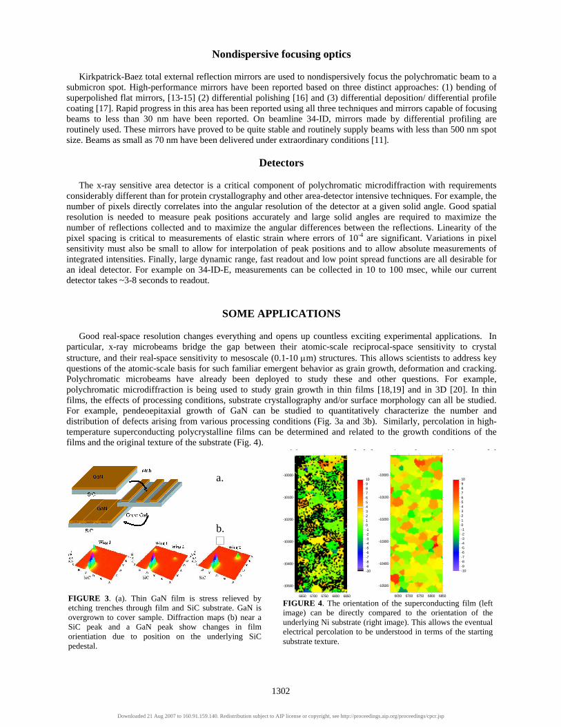
FIGURE 3. (a). Thin GaN film is stress relieved by etching trenches through film and SiC substrate. GaN is overgrown to cover sample. Diffraction maps (b) near a SiC peak and a GaN peak show changes in film orientiation due to position on the underlying SiC pedestal.
Nondispersive focusing optics
Kirkpatrick-Baez total external reflection mirrors are used to nondispersively focus the polychromatic beam to a submicron spot. High-performance mirrors have been reported based on three distinct approaches: (1) bending of superpolished flat mirrors, [13-15] (2) differential polishing [16] and (3) differential deposition/ differential profile
coating [17]. Rapid progress in this area has been reported using all three techniques and mirrors capable of focusing beams to less than 30 nm have been reported. On beamline 34-ID, mirrors made by differential profiling are routinely used. These mirrors have proved to be quite stable and routinely supply beams with less than 500 nm spot size. Beams as small as 70 nm have been delivered under extraordinary conditions [11].
Detectors
The x-ray sensitive area detector is a critical component of polychromatic microdiffraction with requirements considerably different than for protein crystallography and other area-detector intensive techniques. For example, the number of pixels directly correlates into the angular resolution of the detector at a given solid angle. Good spatial resolution is needed to measure peak positions accurately and large solid angles are required to maximize the number of reflections collected and to maximize the angular differences between the reflections. Linearity of the pixel spacing is critical to measurements of elastic strain where errors of 10-4 are significant. Variations in pixel sensitivity must also be small to allow for interpolation of peak positions and to allow absolute measurements of integrated intensities. Finally, large dynamic range, fast readout and low point spread functions are all desirable for an ideal detector. For example on 34-ID-E, measurements can be collected in 10 to 100 msec, while our current detector takes ~3-8 seconds to readout.
SOME APPLICATIONS
Good real-space resolution changes everything and opens up countless exciting experimental applications. In particular, x-ray microbeams bridge the gap between their atomic-scale reciprocal-space sensitivity to crystal structure, and their real-space sensitivity to mesoscale (0.1-10 μm) structures. This allows scientists to address key questions of the atomic-scale basis for such familiar emergent behavior as grain growth, deformation and cracking. Polychromatic microbeams have already been deployed to study these and other questions. For example, polychromatic microdiffraction is being used to study grain growth in thin films [18,19] and in 3D [20]. In thin films, the effects of processing conditions, substrate crystallography and/or surface morphology can all be studied. For example, pendeoepitaxial growth of GaN can be studied to quantitatively characterize the number and distribution of defects arising from various processing conditions (Fig. 3a and 3b). Similarly, percolation in high-temperature superconducting polycrystalline films can be determined and related to the growth conditions of the films and the original texture of the substrate (Fig. 4).
Measurements of deformation also provide powerful insights into the role of mesoscale structure on local defect development and survival. For example, 3D measurements of deformation can now be related to surface measurements of deformation to understand how the near surface region behaves distinctly from the core regions. These studies have now been carried out near grain boundaries, triple junctions and other distinct mesoscale structure to begin the quantifying the driving forces and processes that lead to collective and emergent behavior in deformation. Similarly, studies of crack organization and length scales are underway.
NEW INSTRUMENTATION AND SCIENTIFIC DIRECTIONS
6650 6700 6750 6800 6850
-10500
-10400
-10300
-10200
-10100
-10000
-10-9-8-7-6-5-4-3-2-1012345678910
6650 6700 6750 6800 6850
-10500
-10400
-10300
-10200
-10100
-10000
-10-9-8-7-6-5-4-3-2-1012345678910
FIGURE 4. The orientation of the superconducting film (left image) can be directly compared to the orientation of the underlying Ni substrate (right image). This allows the eventual electrical percolation to be understood in terms of the starting substrate texture.
a. b.
1302
Downloaded 21 Aug 2007 to 160.91.159.140. Redistribution subject to AIP license or copyright, see http://proceedings.aip.org/proceedings/cpcr.jsp

-300 -200 -100 0 100 200 300
5000
10000
15000
20000
25000
30000
Inte
nsity
position (nm)
FWHM ~ 80 nmwhite beam
FIGURE 5. Beams below 30 nm have been reported for KB mirrors, and we have recently focused polychromatic beams to less than 80 nm.
FIGURE 6. (top) Multiple mirrors can be used to increase the divergence in each plane. This reduces the ultimate diffraction limit but leads to structure in the focal plane intensity distribution 6 (bottom).
Ultra-Small Beams
The increasing importance of nanomaterials requires ultra-small probes of materials properties with spatial resolution to resolve individual nanoparticles or to resolve nanoscale volumes in larger samples. For polychromatic radiation, total-external-reflection Kirkpatrick Baez optics have an intrinsic limit of around 30 nm in spot size which is being approached with ever more perfect optics. We have recently demonstrated beams as small as 70 nm using profile coated optics [11] and have measured beams around 80 nm for polychromatic radiation(Fig. 5). There are currently several strategies emerging to produce even smaller beams. For example, Wolter optics can collect ~4 times larger solid angles. which can theoretically produce beam sizes below 8 nm. Similarly, multilayer optics work at larger grazing incidence angles that similarly allows for beams less than 8 nm. However, Wolter optics are challenging to manufacture for hard x-rays and multilayer optics have reduced bandpass that limits some polychromatic microdiffraction applications. A possible alternative approach-with its own complications- is to use matched pairs of elliptical mirrors to increase the divergence collected in each plane. As illustrated in Fig. 6a if two mirror elliptical surfaces focus to the same image plane, the effective divergence is 4 times larger than is practical for a single mirror. This means that the FWHM of the central beam has a theoretical diffraction limit 4x smaller than with a single elliptical mirror (8 nm). However, because the divergence is not uniform, there will be significant intensity in the region near the central peak (Fig. 6c). We note, that this strategy can be used to resolve very small volumes and the divergence can be further increased with additional reflections (Fig. 6b). The complication of additional maxima can be addressed with deconvolution methods, but is an obvious drawback.
Diffuse Scattering From Polycrystalline Samples
One potentially exciting application of the instrumentation developed for polychromatic microdiffraction is the study of defects through diffuse scattering. Diffuse x-ray scattering is a powerful tool for determining defects in single crystals with a long history of contributing to our understanding of materials properties. However, best measurements are made on good single-crystal samples that are hard to obtain and as discussed below may even be dangerous. Small polycrystalline sample are however plentiful and easy to prepare for investigations by x-ray microbeams. Because the sample does not need to rotate, thin film samples with grains as small as 10 to 20 μm are sufficient to ensure that the diffraction signal is from a single crystal. This opens up the field of diffuse scattering to a range of samples that would be hard to prepare and invites scientists to address questions that were previously difficult or impossible to answer. For example, we have recently proposed studies of radiation damage in large-grained polycrystalline thin-film samples. Such samples can provide information about primary defects and about factors that influence the survival of these defects. Of great importance is the fact that these samples can be some 5 to 7 orders of magnitude lower in activity than traditional single-crystal samples prepared with the same composition and dose.
1303
Downloaded 21 Aug 2007 to 160.91.159.140. Redistribution subject to AIP license or copyright, see http://proceedings.aip.org/proceedings/cpcr.jsp
Other science also possible includes measurements of local structural fluctuations and measurements of the response of defects to various sinks. Already there have been preliminary measurements in these areas, but the power of nondispersive optics to probe full reciprocal space volumes without changing the real-space sample volume will make these measurements much more sensitive and straightforward.
Accelerated 3D Data Collection
Although 2D maps of thin films and high-density samples can be collected in a few hours, 3D volume maps by differential aperture microscopy are extremely time consuming and virtually impossible for real-time measurements of dynamics. Faster detectors and more advanced data collection can change this situation and efforts are underway to procure 100 hz cameras and to develop new and faster methods of coding the beam position. With a 100 hz camera, images can be collected at about 10-50 hz depending on the sample. This is about 20-500 times faster than with our current detector. At this rate, even straightforward differential aperture microscopy can collect significant volumes with ~500K voxels in 2-5 hours. If multiple apertures or backgammon techniques are employed, an additional gain of about 10 can be expected so that volume information can be collected in about 10-30 minutes.
ACKNOWLEDGMENTS
Work sponsored by the U.S. Department of Energy, Division (DOE), Division of Materials Sciences and Engineering. Oak Ridge National Laboratory (ORNL) is operated by UT-Battelle, LLC, for the U.S. Department of Energy under contract DE-AC05-00OR22725. Experiments were performed on Unicat beamline 34-ID at the Advanced Photon Source Argonne Il. Both 34-ID and the APS are supported by the DOE Office of Basic Energy Science.The submitted manuscript has been authored by a contractor of the U.S. Government under contract No. DE-AC05-00OR22725. Accordingly, the U.S. Government retains a nonexclusive, royalty-free license to publish or reproduce the published or reproduce the published form of this contribution, or allow others to do so, for U.S. Government purposes.
REFERENCES
1. J.S. Chung and G.E. Ice, J. Appl. Phys. 86 5249-5256 (1999). 2. M. von Laue, Nobel Lecture, http://nobelprize.org/physics/laureates/1914/laue-lecture.pdf (1915). 3. W. Liu, G.E. Ice, B.C. Larson, W. Yang and J. Tischler, Met and Mat. Trans. A. 35A 1963-1967 (2004). 4. Warren, B. E. X-Ray Diffraction, Dover Publications pg. 19 (1990). 5. G.E. Ice, J.-S. Chung, B.C. Larson, J.D. Budai, J.Z. Tischler, N. Tamura, and W. Lowe, AID Conf. Proc. 521 19 (2000). 6. R. I. Barabash, G.E. Ice, B.C. Larson, G.M. Pharr, K.-S. Chung and W. Yang, Appl. Phys. Lett. 79 749 (2001). 7. Larson, B. C., Yang, W., Ice, G. E., Budai, J. D. and Tischler, J. Z., Nature, 415, 887-890 (2002). 8. Ice, G. E., Chung, J. S., Lowe, W., Williams, E. and Edelman, J. Rev. Sci. Instr., 71, 2001-2006 (2000). 9. P. Kirkpatrick and A.V. Baez, J. Opt. Soc. Am. 38 766 (1948). 10. Ice, G. E., Chung, J. S., Tischler, J. Z., Lunt, A. and Assoufid, L. Review of Scientific Instruments, 71, 2635-2639 (2000). 11. W. Liu, Gene E. Ice, Jonathan Z. Tischler, Ali Khounsary, Chian Liu, Lahsen Assoufid, and Albert T. Macrander, Rev. Sci.
Instrum. 76, 113701 (2005). 12. N. Tamura, A.A. Macdowell, R. Spolenak, B.C.Valek, J.C. Bravman, W.L. Brown, R.S. Celestre, .A. Padmore, B.W.
Batterman, J.R. Patel, J. of Synch. Rad. 10 137-143 (2003). 13. P.J. Eng, M.L. Rivers, X. Bingxin and W. Schildkamp SPIE 2516 41 (1995). 14. O. Hignette, P. Cloetens, W. K. Lee, W. Ludwig and G. Rostaing, Journal de Physique IV 104 231-234 (2003). 15. M.R. Howells, D. Cambie, R.M. Duarte, S. Irick, A. Macdowell, H. A. Padmore, T. Renner, S. Rah and R. Sander, Opt. Eng.
39 2748 (2000). 16. K. Yamauchi, K. Yamamura, H. Mimura, Y. Sano, A. Saito, A. Souvorov, M. Yabashi, K. Tamasaku, T. Ishikawa and Y.
Mori, J. Sync. Rad. 9 313 (2002). 17. C. Liu, Lahsen Assoufid, R. conley, A. Macrander, G.E. Ice and J.Z. Tischler, Opt. Eng. 42 3622 (2003). 18. R.I. Barabash, G.E. Ice, W. Liu, S. Einfldt, D. Hommel, A.M. Roskowski and R.F. Davis, Phys. Stat. Sol. A 5 732 (2005). 19. J.D. Budai, W.G Yang, N. Tamura, J.S. Chung, J.Z. Tischler, B.C. Larson, G.E. Ice, C. Park, and D.P. Norton. Nat. Mat. 2
487-492 (2003). 20. J.D. Budai, M. yang, B.C. Larson, J.Z. Tischler, W. Liu, H. Weiland and G.E. Ice, Nat. Sci. Forum 467-470 1373-1378
(2004).
1304
Downloaded 21 Aug 2007 to 160.91.159.140. Redistribution subject to AIP license or copyright, see http://proceedings.aip.org/proceedings/cpcr.jsp