Platinum Electrodeposition on Unsupported Single Wall Carbon Nanotubes and Its Application as...
8
doi: 10.1149/2.054302jes 2013, Volume 160, Issue 2, Pages H98-H104. J. Electrochem. Soc. Magen, Miguel José-Yacaman, Jing Li and Carlos R. Cabrera Enid Contes-de Jesus, Diana Santiago, Gilberto Casillas, Alvaro Mayoral, Cesar Sensing Material Carbon Nanotubes and Its Application as Methane Platinum Electrodeposition on Unsupported Single Wall service Email alerting click here in the box at the top right corner of the article or Receive free email alerts when new articles cite this article - sign up http://jes.ecsdl.org/subscriptions go to: Journal of The Electrochemical Society To subscribe to © 2012 The Electrochemical Society
-
Upload
independent -
Category
Documents
-
view
0 -
download
0
Transcript of Platinum Electrodeposition on Unsupported Single Wall Carbon Nanotubes and Its Application as...

doi: 10.1149/2.054302jes2013, Volume 160, Issue 2, Pages H98-H104.J. Electrochem. Soc.
Magen, Miguel José-Yacaman, Jing Li and Carlos R. CabreraEnid Contes-de Jesus, Diana Santiago, Gilberto Casillas, Alvaro Mayoral, Cesar Sensing MaterialCarbon Nanotubes and Its Application as Methane Platinum Electrodeposition on Unsupported Single Wall
serviceEmail alerting
click herein the box at the top right corner of the article or Receive free email alerts when new articles cite this article - sign up
http://jes.ecsdl.org/subscriptions go to: Journal of The Electrochemical SocietyTo subscribe to
© 2012 The Electrochemical Society
H98 Journal of The Electrochemical Society, 160 (2) H98-H104 (2013)0013-4651/2013/160(2)/H98/7/$28.00 © The Electrochemical Society
Platinum Electrodeposition on Unsupported Single Wall CarbonNanotubes and Its Application as Methane Sensing MaterialEnid Contes-de Jesus,a Diana Santiago,a,∗ Gilberto Casillas,b Alvaro Mayoral,cCesar Magen,c,e Miguel Jose-Yacaman,b Jing Li,d,∗ and Carlos R. Cabreraa,∗,z
aNASA-URC Center for Advanced Nanoscale Materials, Department of Chemistry, University of Puerto Rico, RıoPiedras Campus, San Juan 00936-8377, Puerto RicobDepartment of Physics and Astronomy, University of Texas at San Antonio, One UTSA Circle, 78249 San Antonio,Texas, USAcLaboratorio de Microscopias Avanzadas, Instituto de Nanociencia de Aragon, Universidad de Zaragoza, 50018Zaragoza, SpaindCenter for Nanotechnology, NASA Ames Research Center, Moffett Field, California 94035, USAeDepartamento de Fisica de la Materia Condensada, Universidad de Zaragoza, 50009 Zaragoza, Spain
This paper reports the decoration of single wall carbon nanotubes (SWCNTs) with platinum (Pt) nanoparticles using an electrochem-ical technique, rotating disk slurry electrode (RoDSE). Pt/SWCNTs were electrochemically characterized by cyclic voltammetrytechnique (CV) and physically characterized through the use of transmission electron microscopy (TEM), energy dispersive spec-troscopy - X-ray florescence (EDS-XRF) and X-ray diffraction (XRD). After characterization it was found that electrodepositednanoparticles had an average particle size of 4.1 ± 0.8 nm. Pt/SWCNTs were used as sensing material for methane (CH4) detectionand showed improved sensing properties in a range of concentration from 50 ppm to 200 ppm parts per million (ppm) at roomtemperature, when compared to other Pt/CNTs-based sensors. The use of this technique for the preparation of Pt/SWCNTs opens anew possibility in the bulk preparation of samples using an electrochemical method and thus their potential use in a wide variety ofapplications in chemical sensing, fuel cell and others.© 2012 The Electrochemical Society. [DOI: 10.1149/2.054302jes] All rights reserved.
Manuscript submitted July 30, 2012; revised manuscript received November 19, 2012. Published December 1, 2012.
Carbon nanotubes (CNT) have been the focus of numerous studiessince their discovery in 1991.1 CNTs have been proposed as ideal ma-terials for different potential applications2–4 including energy storage,5
nanoelectronics,6 chemical sensors,7,8 and biosensors,9 among oth-ers. Single wall carbon nanotubes (SWCNTs) possess characteristics3
such as high surface area, high thermal and mechanical stability, andfunctionalization capability, which make them suitable as matrix forsupporting nanoparticles (NPs).
Pt/SWCNTs composites are prepared by various syntheticmethods10–12 including impregnation, precipitation, colloidal, sputter-ing, and others, which offer large-scale production. Electrodepositiontechnique has shown advantages over the aforementioned methods dueto the fact that particle size, distribution and loading of metal particlescan be controlled by the variation of time, applied potential and con-centration. However, conventional electrochemical deposition of PtNPs on SWCNTs has been possible when SWCNTs were grown, castor chemically attached to a substrate or were used in the form of thinfilm or foil7,13 which limits the production quantity of Pt/SWCNTscomposite for its use in real applications.
Cabrera’s research group recently reported the use of the rotatingdisk-slurry electrode (RoDSE) technique for the large-scale produc-tion of well-dispersed Pt NPs on unsupported carbon black.14 In thispaper we report the use of the RoDSE technique for the bulk prepara-tion of Pt/SWCNTs. The purpose of the current work is to demonstratethat it is possible to electrodeposit Pt NPs onto unsupported SWC-NTs. In addition, to show a potential application, where we used theprepared Pt/SWCNTs as sensing material for the ppm level detectionof CH4 at room temperature.
Experimental
SWCNTs purification and oxidation.— SWCNTs (Carbon Nan-otechnologies) were purified to remove iron catalyst. Briefly, the asreceived SWCNTs were refluxed in nitric acid (HNO3) 2.6 M at 200◦Cfor 24 hours. Dilution, decantation and centrifugation were performedin order to increase the pH above 3, followed by filtration using a Mil-lipore system and vacuum pump and rinsed thoroughly with nanopurewater (Barnsted). The purified SWCNTs were oven dried at 150◦Cfor 3 hours. In order to obtain o-SWCNTs, the purified SWCNTs
∗Electrochemical Society Active Member.zE-mail: [email protected]
were suspended in a 3:1 mixture of H2SO4 (Optima) and HNO3 andsonicated for 8 hours at 35–40◦C. Dilution, decantation and centrifu-gation were repeated followed by filtration and rinsing. The samplewas allowed to dry at room temperature.
Pt electrodeposition on SWCNTs (Pt/SWCNTs).— A slight vari-ation of the RoDSE procedure reported by our group14,15 wasperformed. In brief, 30 mg of o-SWCNTs were mixed withH2SO4 0.1 M and 2 mL of K2PtCl6 5 mM dissolved in H2SO4
0.1 M, sonicated for 1 hour to form the slurry. The slurry was thentransferred to the center tube of a 3-electrode cell (3 compartmentsseparated by fritted glass, one for each electrode). An illustration ofthe 3-electrode cell can be found in reference.15 A glassy carbon RDE,Ag/AgCl (0.197 V vs. NHS) and a graphite rod were used as working,reference and counter electrodes, respectively. The electrodepositionprocess was done by placing the working electrode in the slurry andwith an angular velocity of 900 rpm. Under a nitrogen atmosphere,a constant voltage of −0.2 V vs Ag/AgCl was applied for 2 hours.This process was repeated 4 consecutive times and the changes of cur-rent as function of time (chronoamperometry) were recorded. Whenthe electrodeposition was completed, the slurry was removed fromthe cell, filtrated and rinsed thoroughly with nanopure water in orderto remove residues of non-reduced species, or free standing Pt NPs,if any.
Ink paste preparation and electrode modification.— Glassy car-bon electrodes (GCE) (diameter: 3 mm Bioanalytical System) weremechanically polished with alumina (1.0, 0.3 and 0.05 μm) and rinsedthoroughly with nanopure water. The electrodes were then sonicated inethanol and nanopure water in order to remove any alumina residuesand air-dried at room temperature. An ink paste was prepared bymixing 0.5 mg of the sample (o-SWCNTs or Pt/SWCNTs) with700 μL of dimethylformamide (DMF) and 50 μL of Nafion 5wt%and sonication for 1 hr. An 8 μL droplet of the ink paste was cast overthe surface of the GCE. The modified electrode was then allowed toair-dry overnight and ready for electrochemical characterization.
Electrochemical characterization.— All electrochemical mea-surements were done in 0.50 M H2SO4. A three-electrode cell usingthe modified GCE as working electrode, Ag/AgCl as reference elec-trode, a Pt wire as counter electrode and with a Basic ElectrochemicalSystem (EG&G). All the potentials are reported vs. Ag/AgCl.

Journal of The Electrochemical Society, 160 (2) H98-H104 (2013) H99
CV.—CV for o-SWCNTs samples was done at potentials from −0.2to 0.9 V vs. Ag/AgCl and at a scan rate of 100 mV sec−1. Pt/SWCNTssamples were cycled between −0.22 and 1.2 V vs. Ag/AgCl, at a scanrate of 1 mV sec−1.CO stripping.—For the CO stripping experiment, CO was bubbled intothe 3-electrode cell for 15 minutes at an applied potential of 0.100 Vvs. Ag/AgCl. Then, Ar was bubbled for another 15 minutes to displacethe CO from solution. Afterwards, two consecutive scan cycles wereperformed at potentials between −0.2 and 0.9 V vs. Ag/AgCl, at ascan rate of 20 mV sec−1.
Surface characterization.— To study and track the changes incomposition and morphology, different techniques for surface analysiswere used. X-ray photoelectron spectroscopy (XPS) data was acquiredusing a PHI 5600 ci spectrometer with monochromatic Al-Kα source.To obtain the survey analysis, the spectra were recorded at a takeoff angle and pass energy of 45◦ and 187.85 eV, respectively. Energydispersive spectroscopy-X-ray fluorescence (EDS-XRF) (JEOL JSM-5800LV) was used for elemental analysis. X-ray diffraction (XRD)analysis was done using a Rigaku Ultima II diffractometer and Kαincident X-ray source. Scans were recorded between 20 and 90◦ inthe 2θ range, step size of 0.02◦ and a speed of 1.00 deg min−1.
Transmission electron microscopy (TEM) images were obtainedusing a TITAN 60-300 cubed, operated at 80 kV. The spherical aber-rations were corrected trough a CESCOR corrector for the objectivelens, reaching a 0.8-angstrom point resolution. The cube maintainedthe equipment isolated from any external vibration. The images wererecorded for 0.4 seconds each. Nanostructures were characterized in aJEOL JEM-ARM200F electron microscope operated in STEM mode.
Sensor preparation and gas sensing experiments.— Figure 1shows the printed circuit board (PCB) chip containing 16 interdig-itated electrodes (IDEs) used for the gas sensing experiments with asimilar platform as those previously reported by Y. Lu, et al.16,17 EachIDE has fingers with a width of 80 μm and gap distance betweenfingers of 115 μm. The o-SWCNTs and Pt/SWCNTs nanomaterialswere suspended in DMF (0.018%w/w) and sonicated. The sampleswere then deposited over sensors using a micropipette. After sampledeposition, the sensors were baked (80oC and vacuum) to removepossible solvent traces adhered to the sample. An initial resistanceof several hundreds k� was obtained from made sensors. Each testwas repeated at least three times for reproducibility purposes. The
Figure 1. Picture of printed circuit board (PCB) chip (IDE) containing 16interdigitated electrodes (IDEs) used for the gas sensing experiments witha similar platform as those previously reported by Y. Lu, et al.16,17 EachIDE has fingers with a width of 80 μm and gap distance between fingers of115 μm.
sensors were exposed to CH4 at concentrations of 50, 100, 125 and200 ppm provided by an Environics 2040, a gas blending and dilutionsystem using air as purge and diluting gas at constant flow rate of400 cm3/min. Sensing experiments were carried out as follows: sen-sors were initially exposed to air for 35 minutes to establish a baselineand then exposed to CH4 for 3 minutes at each concentration and5 minute purge in between concentrations. All gas-sensing exper-iments were carried out at room temperature and with 40% rela-tive humidity (RH). Changes in resistance as function of time wererecorded using a customized LabVIEW program. Relative responsesfor each concentration were calculated using the following equation:Rrel = (Ri−R0)
R0, where R0 is the initial resistance before each CH4 ex-
posure and Ri is the resistance of the sensor during the CH4 exposure.The noise (N) of the sensors was determined by calculating the rootmean square (rms) of the baseline. Responses with a signal to N ratio(s/N) greater or equal to 3 were considered. Calibration curves wereobtained by making a graph of (Ri − R0) as function of concentra-tion. The slope of the calibration curve is the sensitivity. Finally, thedetection limit (DL) of each sensor was calculated with the followingequation: 3(rms/slope).
Results and Discussion
Purification-oxidation process.— The purification process ofSWCNTs was carried out to eliminate the iron particles that are usedas catalyst (Fe-catalyst) in their production and is important becausethese particles might interfere in some applications as well as in elec-trochemical studies. Figure 2 shows the XPS survey analysis spectrafor as-received SWCNTs and oxidized SWCNTs (o-SWCNTs). It canbe observed the elimination of the peaks corresponding to Fe2p, afterthe processes of purification and oxidation. It is also noticeable anincrease in the intensity of the O1s signal for o-SWCNTs relative tothat of as-received SWCNTs, as a result of the oxidation process.
Relative elemental composition of the samples is shown in Table Iand it suggests the removal of the Fe-catalyst. However, it is wellknown that traces of Fe will always be present. An increase in the
Figure 2. X-ray photoelectron spectroscopy survey spectra for as-receivedSWCNTs and o-SWCNTs.

H100 Journal of The Electrochemical Society, 160 (2) H98-H104 (2013)
Table I. Relative atomic composition for as received andoxidized SWCNTs obtained by X-ray photoelectron spectroscopy.The elemental composition data was used to determine theoxygen-carbon atomic ratio.
SWCNTs sample C 1s% O1s% Fe2p% O/C
as received SWCNTs 91.39 6.94 1.25 0.08o-SWCNTs 79.04 20.96 0.00 0.27
relative amount of O1s after the purification and oxidation processescan also be noticed. Values from Table I were also used to calculatethe oxygen to carbon atomic ratio (O/C). Before purification, the O/Cvalue was 0.08. After the purification process, the O/C was 0.27, whichis 3.4 times larger than the as-received SWCNTs. In fact, the O/C valueof 0.27 is comparable with the O/C of 0.25 reported by Cabrera’sresearch group after treating SWCNTs with a similar purification-oxidation process.18 Cyclic voltammetry (CV) was also performedto as received and o-SWCNTs samples. When comparing the twovoltammograms shown in Figure 3, it can be observed that for o-SWCNTs sample, there is an increase in the capacitance double layerdue to an increase in the oxygen surface concentration that resultedfrom the acid treatment.19,20 In the same way, two broad peaks around0.4 V vs. Ag/AgCl can be observed and they are attributed to oxygen-containing functional groups like carboxylic acids and quinines.19,21
Figure 4 shows a TEM micrograph of a clean single wall carbonnanotubes with a diameter of 1 nm. It is also important to note that theoxidation processes was aggressive enough to create functionalitiesbut without losing the SWCNTs structure.
Electrodeposition process.— In order to do the electrodepositionprocess it is very important to have the o-SWCNTs suspended inaqueous slurry. Considering their highly hydrophobic nature, theoxygen-containing groups in the SWCNTs created during the pu-rification/oxidation process help to improve their wettability, and thuson the formation of the slurry. Once the slurry is placed on the celland in contact with the glassy carbon rotating disk electrode RDE(working electrode), the electrodeposition process is carried out. Dur-ing the electrodeposition process the rotation of the RDE creates ahydrodynamic flow that keeps the slurry in movement and suspendedin the cell. Pt NPs are electrodeposited over the SWCNTs as theyreach the surface of the RDE while a potential of −0.2 V is constantlyapplied. The amount of Pt electrodeposited on SWCNTs (Pt loading)was determined using an Inductively Coupled Plasma- Mass Spec-trophotometer (ICP-MS). The average loading of the samples was1.22 ± 0.13% w/w. Comparable results were obtained with XPS andEDS-XRF analysis.
Figure 4. Transmission electron microscopy micrograph of o-SWCNTs.
Two potential situations were identified while using RoDSE tech-nique. The first one is that the working electrode is material is glassycarbon, which is also carbonaceous material and it is expected thatPt may deposit on its surface instead of SWCNTs. The second one isrelated to the reduction reaction from PtCl6
−2 to Pt0:
PtCl−26 + 2e− → PtCl+2
4 + 2Cl− [1a]
PtCl+24 + 2e− → Pt0 + 4Cl− [1b]
Considering the reduction reaction presented above, there is possibil-ity of having intermediates (partially reduced Pt+2 species) trappedwithin the SWCNTs due to defects in their structure created duringthe purification-oxidation process and/or between entangled SWC-NTs. However, these are not considered to be major problems sincethe objective of electrodepositing Pt NPs on SWCNTs was met, asdemonstrated with electrochemical and surface characterization thatare discussed in the following sections.
Figure 3. Cyclic voltammetries in 0.50 M H2SO4 at100 mV sec−1 for as-received and o-SWCNTs.

Journal of The Electrochemical Society, 160 (2) H98-H104 (2013) H101
Figure 5. Cyclic voltammetry of Pt/SWCNTs in0.50 M H2SO4 at 100 mV sec−1.
Electrochemical characterization.— To perform electrochemicalcharacterization, the Pt/SWCNTs samples, prepared by the RoDSEtechnique, were prepared into an ink-paste and cast over a glassy car-bon electrode (GCE). Figure 5 shows the CV of Pt/SWCNTs donein 0.50 M H2SO4 at 100 mv/sec. The CV shows small peaks corre-sponding to hydrogen adsorption and desorption on Pt NPs. It alsoshows the peaks at around 0.4 V corresponding to oxygen-containingfunctional groups of the o-SWCNTs. Since carbon monoxide (CO) isadsorbed on Pt active sites (poisoning), CO stripping was performedto determine electrochemically active surface area (EAS) (Fig. 6). Af-ter the exposure of the sample to CO, the CO stripping peak potentialappeared at around 0.6 V vs. Ag/AgCl. To calculate the CO strippingcharge, the area under the peak was integrated and the charge corre-sponding to the double layer was subtracted. The obtained charge was3.708 × 10−5 C. This value was used to calculate the CO surface areain cm2 was calculated using the following equation:22
SC O = QC O
0.420mC cm−2[2]
where QCO is the CO stripping charge (mC) and 0.420 mC cm−2 isthe monolayer of the CO adsorbed. The obtained EAS was 139 m2/gof Pt.
Surface characterization and elemental analysis.— EDS-XRFwas used to obtain elemental analysis of the sample and the spec-trum is shown in Figure 7. The presence of Pt was detected as well asthe presence of chlorine (Cl), potassium (K) and Fe, which correspondto ligands and counter ions of the Pt salt precursor used during theelectrodeposition process and remaining traces of catalyst (SWCNTsformation), respectively.
TEM and scanning electron transmission microscopy (STEM) im-ages were recorded in order to observe the Pt NPs electrodepositedover the SWCNTs. Figure 8 shows bright field (BF) TEM micrographsof the Pt/SWCNTs sample. Well-dispersed, small dark particles thatcorrespond to NPs and small clusters of Pt over the SWCNTs bundlesare shown in Figure 8a. Pt NPs with diameters smaller than 10 nmcan be observed in Figure 8b. Figure 9a shows the graph of particlesize distribution obtained from the TEM image shown in Figure 9b.
Figure 6. Electrochemical CO stripping. First two cycles after CO exposure done in H2SO4 0.5 M at 20 mV sec−1.

H102 Journal of The Electrochemical Society, 160 (2) H98-H104 (2013)
Figure 7. Energy dispersive spectroscopy- X-ray fluorescence spectra for Pt/SWCNTs.
The average size of particles is 4.1 ± 0.8 nm and this value is similarto the 5 ± 2 nm size for Pt NPs prepared by the RoDSE technique.14
XRD data was used to analyze the Pt NPs crystalline structures (seeFigure 10). The o-SWCNTs sample showed peaks around 2θ = 25◦
and 42◦ assigned to C (002) and C (100), respectively, and correspondto the graphitic structure of the SWCNTs. The Pt containing sampleshowed the characteristics peaks of Pt with a face cubic centered (FCC)structure. The diffraction peaks at 2θ of ca. 39.5◦, 46.5◦, 67.5◦, 81.5◦
and 86◦ correspond to Pt (111), (200), (311) and (222), respectively.23
It also shows the peak corresponding to C (002), which means thatthe SWCNTs conserved its crystalline graphitic structure, even afterthe purification and oxidation processes that are well known to dam-age their structure. Using the peak Pt (111) and Scherrer’s equation(d = 0.89λKα1/B2θ cos θmax) the average crystallite size is estimatedto be 5.4 nm, which is comparable to the value obtained for Pt particlesize from TEM.
CH4 detection.— Theoretical and experimental studies havedemonstrated that sensors based on pristine CNTs have poor sen-sitivity detecting non-polar gases mainly due to its chemical stabilityfrom their strong sp2 bonds and weak sp3 bonds at the tube ends whichgive the inability of the CH4 molecules to accept or donate electronsand subsequently cannot produce the changes in the conductance ofCNTs.24,25 Taking advantage of their modification capability, CNTsmodified with functional groups, dopants, metallic NPs, metal-oxideNPs and polymers have shown to overcome this limitation. Severalreviews focused on modified CNTs for gas sensor applications havebeen recently published.8,26–29
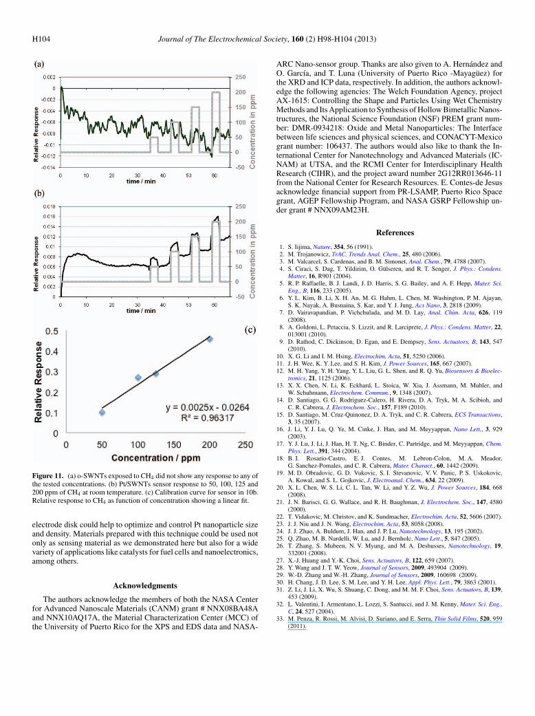
All CH4 sensing experiments were carried out with 40% RHpresent, at room temperature with a constant flow of 400 cm3/min. Asobserved in Figure 11a, o-SWNTs samples did not show any changesin resistance for any of the tested concentrations. A typical sensorresponse of Pt/SWNTs for CH4 detection showing an increase in re-sistance can be observed as CH4 was introduced (Figure 11b). Sensor’sresponse is a relative change of its resistance defined as:
Rrel = (Ri − R0)
R0[3]
where R0 is the initial resistance before CH4 exposure and Ri is theresistance of the sensor during the CH4 exposure. Calibration curve(Figure 11c) from the sensor responses shows that a linear fit best
describes the relation of the sensor’s responses as function of CH4
concentration.The results obtained in this work are in good agreement with previ-
ous theoretical and experimental results for other CNT-based sensorsused for CH4 detection.24,30,31 As suggested by L. Valentini et al. theincrease in resistance can be attributed to CH4 acting as an electrondonor and thus reducing the hole density in the P-type Pt/SWNTscomposite.32 Pt/SWCNTs sensors were able to detect the lower testedconcentration (50 ppm) and showed to have good reversible at roomtemperature. Here, we demonstrate an improvement in sensitivity andoperation temperature of the Pt/SWCNTs sensors, when compared tothe work recently published in which Pt/MWCNTs sensors were forthe detection of CH4 (98–5600 ppm) at 120◦C.33
Conclusions
Unsupported SWCNTs were successfully modified with Pt NPsusing the RoDSE technique. To best of our knowledge, this is thefirst time that an electrodeposition method is used for the bulk pro-duction of Pt/SWCNTs. The as-received SWCNTs were purified andoxidized before Pt electrodeposition. XPS and CV confirmed removalof the Fe-catalyst and increase in concentration of oxygen-containinggroups in SWCNTs. During the electrodeposition process, a slurrysolution containing suspended o-SWCNTs was used and a constantapplied potential was done via the RDE. With this technique, Pt waselectrodeposited on SWCNT with an average loading of 1.22% w/w.The EDS-XRF elemental analysis confirmed the presence of Pt aswell as Cl and K, which are components of the Pt precursor salt andXRD data showed that the electrodeposited Pt0 has FCC structure.TEM images showed the presence of electrodeposited Pt atoms, atomclusters, and NPs with an average size of 4.1 ± 0.8 nm.
The possibility of using the Pt/SWCNTs for gas sensing appli-cation was demonstrated. This electrochemically Pt modified un-supported SWCNT proved to be an excellent sensing material forppm level detection of CH4 at room temperature. From the cal-ibration curve, the sensor’s responses were proportional to CH4
concentrations.We consider that this work opens a new and alternative way to pre-
pare metallic NPs supported on SWCNTs in large-scale. Furthermore,optimization of various parameters like the metal precursor concen-tration, deposition time and angular velocity of the rotating working

Journal of The Electrochemical Society, 160 (2) H98-H104 (2013) H103
Figure 8. Bright Field-Transmission electron microscopy images ofPt/SWCNTs.
Figure 9. Graph of particle size distribution (a) from transmission electronmicroscopy image (b).
Figure 10. X-ray diffraction patterns for o-SWCNTs and Pt/SWCNTs samples.
H104 Journal of The Electrochemical Society, 160 (2) H98-H104 (2013)
Figure 11. (a) o-SWNTs exposed to CH4 did not show any response to any ofthe tested concentrations. (b) Pt/SWNTs sensor response to 50, 100, 125 and200 ppm of CH4 at room temperature. (c) Calibration curve for sensor in 10b.Relative response to CH4 as function of concentration showing a linear fit.
electrode disk could help to optimize and control Pt nanoparticle sizeand density. Materials prepared with this technique could be used notonly as sensing material as we demonstrated here but also for a widevariety of applications like catalysts for fuel cells and nanoelectronics,among others.
Acknowledgments
The authors acknowledge the members of both the NASA Centerfor Advanced Nanoscale Materials (CANM) grant # NNX08BA48Aand NNX10AQ17A, the Material Characterization Center (MCC) ofthe University of Puerto Rico for the XPS and EDS data and NASA-
ARC Nano-sensor group. Thanks are also given to A. Hernandez andO. Garcıa, and T. Luna (University of Puerto Rico -Mayaguez) forthe XRD and ICP data, respectively. In addition, the authors acknowl-edge the following agencies: The Welch Foundation Agency, projectAX-1615: Controlling the Shape and Particles Using Wet ChemistryMethods and Its Application to Synthesis of Hollow Bimetallic Nanos-tructures, the National Science Foundation (NSF) PREM grant num-ber: DMR-0934218: Oxide and Metal Nanoparticles: The Interfacebetween life sciences and physical sciences, and CONACYT-Mexicogrant number: 106437. The authors would also like to thank the In-ternational Center for Nanotechnology and Advanced Materials (IC-NAM) at UTSA, and the RCMI Center for Interdisciplinary HealthResearch (CIHR), and the project award number 2G12RR013646-11from the National Center for Research Resources. E. Contes-de Jesusacknowledge financial support from PR-LSAMP, Puerto Rico Spacegrant, AGEP Fellowship Program, and NASA GSRP Fellowship un-der grant # NNX09AM23H.
References
1. S. Iijima, Nature, 354, 56 (1991).2. M. Trojanowicz, TrAC, Trends Anal. Chem., 25, 480 (2006).3. M. Valcarcel, S. Cardenas, and B. M. Simonet, Anal. Chem., 79, 4788 (2007).4. S. Ciraci, S. Dag, T. Yildirim, O. Gulseren, and R. T. Senger, J. Phys.: Condens.
Matter, 16, R901 (2004).5. R. P. Raffaelle, B. J. Landi, J. D. Harris, S. G. Bailey, and A. F. Hepp, Mater. Sci.
Eng., B, 116, 233 (2005).6. Y. L. Kim, B. Li, X. H. An, M. G. Hahm, L. Chen, M. Washington, P. M. Ajayan,
S. K. Nayak, A. Busnaina, S. Kar, and Y. J. Jung, Acs Nano, 3, 2818 (2009).7. D. Vairavapandian, P. Vichchulada, and M. D. Lay, Anal. Chim. Acta, 626, 119
(2008).8. A. Goldoni, L. Petaccia, S. Lizzit, and R. Larciprete, J. Phys.: Condens. Matter, 22,
013001 (2010).9. D. Rathod, C. Dickinson, D. Egan, and E. Dempsey, Sens. Actuators, B, 143, 547
(2010).10. X. G. Li and I. M. Hsing, Electrochim. Acta, 51, 5250 (2006).11. J. H. Wee, K. Y. Lee, and S. H. Kim, J. Power Sources, 165, 667 (2007).12. M. H. Yang, Y. H. Yang, Y. L. Liu, G. L. Shen, and R. Q. Yu, Biosensors & Bioelec-
tronics, 21, 1125 (2006).13. X. X. Chen, N. Li, K. Eckhard, L. Stoica, W. Xia, J. Assmann, M. Muhler, and
W. Schuhmann, Electrochem. Commun., 9, 1348 (2007).14. D. Santiago, G. G. Rodriguez-Calero, H. Rivera, D. A. Tryk, M. A. Scibioh, and
C. R. Cabrera, J. Electrochem. Soc., 157, F189 (2010).15. D. Santiago, M. Cruz-Quinonez, D. A. Tryk, and C. R. Cabrera, ECS Transactions,
3, 35 (2007).16. J. Li, Y. J. Lu, Q. Ye, M. Cinke, J. Han, and M. Meyyappan, Nano Lett., 3, 929
(2003).17. Y. J. Lu, J. Li, J. Han, H. T. Ng, C. Binder, C. Partridge, and M. Meyyappan, Chem.
Phys. Lett., 391, 344 (2004).18. B. I. Rosario-Castro, E. J. Contes, M. Lebron-Colon, M. A. Meador,
G. Sanchez-Pomales, and C. R. Cabrera, Mater. Charact., 60, 1442 (2009).19. M. D. Obradovic, G. D. Vukovic, S. I. Stevanovic, V. V. Panic, P. S. Uskokovic,
A. Kowal, and S. L. Gojkovic, J. Electroanal. Chem., 634, 22 (2009).20. X. L. Chen, W. S. Li, C. L. Tan, W. Li, and Y. Z. Wu, J. Power Sources, 184, 668
(2008).21. J. N. Barisci, G. G. Wallace, and R. H. Baughman, J. Electrochem. Soc., 147, 4580
(2000).22. T. Vidakovic, M. Christov, and K. Sundmacher, Electrochim. Acta, 52, 5606 (2007).23. J. J. Niu and J. N. Wang, Electrochim. Acta, 53, 8058 (2008).24. J. J. Zhao, A. Buldum, J. Han, and J. P. Lu, Nanotechnology, 13, 195 (2002).25. Q. Zhao, M. B. Nardelli, W. Lu, and J. Bernholc, Nano Lett., 5, 847 (2005).26. T. Zhang, S. Mubeen, N. V. Myung, and M. A. Deshusses, Nanotechnology, 19,
332001 (2008).27. X.-J. Huang and Y.-K. Choi, Sens. Actuators, B, 122, 659 (2007).28. Y. Wang and J. T. W. Yeow, Journal of Sensors, 2009, 493904 (2009).29. W.-D. Zhang and W.-H. Zhang, Journal of Sensors, 2009, 160698 (2009).30. H. Chang, J. D. Lee, S. M. Lee, and Y. H. Lee, Appl. Phys. Lett., 79, 3863 (2001).31. Z. Li, J. Li, X. Wu, S. Shuang, C. Dong, and M. M. F. Choi, Sens. Actuators, B, 139,
453 (2009).32. L. Valentini, I. Armentano, L. Lozzi, S. Santucci, and J. M. Kenny, Mater. Sci. Eng.,
C, 24, 527 (2004).33. M. Penza, R. Rossi, M. Alvisi, D. Suriano, and E. Serra, Thin Solid Films, 520, 959
(2011).