![Electron beam induced deposition of rhodium from the precursor [RhCl(PF 3) 2] 2: morphology, structure and chemical composition](https://static.fdokumen.com/doc/165x107/63197481d4191f2f93079c44/electron-beam-induced-deposition-of-rhodium-from-the-precursor-rhclpf-3-2-2.jpg)
Platinum and Rhodium Silicide-Germanide Optoelectronics
44
1 Platinum and Rhodium Silicide-Germanide Optoelectronics M. P. LEPSELTER, 1 A. T. FIORY, 1,2 and N. M. RAVINDRA 2 1.–BTL Fellows, Inc., Summit, NJ 07901. 2.–Department of Physics, New Jersey Institute of Technology, Newark, NJ 07102. ABSTRACT Since the onset of SiO 2 / Si devices in the 1960's, the only basic change in the design of a MOSFET has been in the gate length. The channel thickness has fundamentally remained unchanged, as the inversion layer in a silicon MOSFET is still about 10 nm thick. Bipolar transistor base widths have been of sub-micron dimensions all this time. It is time for a new property to become omnipresent in concert with the high mobility strained-silicon channels and silicon-germanium alloys. This property is the inherently low parasitic series resistance of Schottky barrier contacts. Schottky contacts, beam leads, and microbridges, while originally developed in silicon, have been successfully integrated into compound semiconductors for optoelectronics. Reintroduction of these technologies in optoelectronics based on silicon-germanium is proposed. Several new applications using platinum and rhodium compounds of silicon and germanium are presented. Preprint: Journal of Electronic Materials 37 (2008) pp.403-416. Keywords: Schottky-barrier detectors, high speed, infrared, wavelength selectability, SiGe alloy semiconductors
Transcript of Platinum and Rhodium Silicide-Germanide Optoelectronics

1
Platinum and Rhodium Silicide-Germanide Optoelectronics
M. P. LEPSELTER,1 A. T. FIORY,1,2 and N. M. RAVINDRA2
1.–BTL Fellows, Inc., Summit, NJ 07901. 2.–Department of Physics, New Jersey Institute of Technology, Newark, NJ 07102.
ABSTRACT
Since the onset of SiO2 / Si devices in the 1960's, the only basic change in the design of a MOSFET has been in the gate length. The channel thickness has fundamentally remained unchanged, as the inversion layer in a silicon MOSFET is still about 10 nm thick. Bipolar transistor base widths have been of sub-micron dimensions all this time. It is time for a new property to become omnipresent in concert with the high mobility strained-silicon channels and silicon-germanium alloys. This property is the inherently low parasitic series resistance of Schottky barrier contacts. Schottky contacts, beam leads, and microbridges, while originally developed in silicon, have been successfully integrated into compound semiconductors for optoelectronics. Reintroduction of these technologies in optoelectronics based on silicon-germanium is proposed. Several new applications using platinum and rhodium compounds of silicon and germanium are presented.
Preprint: Journal of Electronic Materials 37 (2008) pp.403-416. Keywords: Schottky-barrier detectors, high speed, infrared, wavelength selectability, SiGe alloy semiconductors
2
INTRODUCTION
This article reviews Schottky-barrier detector (SBD) and beam lead technologies and develops the rationale for new advanced applications in silicon-based optoelectronics. Making novel utilization of silicon compatible materials, the authors present original device concepts and structures for photoreceivers implemented in silicon.
An example of a currently well-established device is the Schottky-barrier photodiode based on the PtSi/p-Si (platinum silicide on p-type silicon) junction, which has been developed for infrared (IR) imaging systems, including forward looking infrared radar, infrared thermal imaging cameras, and multiwavelength imaging pyrometry [1,2]. Some restrictions hobble this particular SBD because it needs to be operated at cryogenic temperatures to suppress the dark current, e.g., cooling focal plane arrays with Stirling cycle engines. Junctions of the type PtSi/n-Si (platinum silicide on n type Si), which need no cooling because of a higher intrinsic Schottky barrier height (0.84 eV vs. 0.26 eV), are suitable for detectors spanning the spectrum from ultraviolet to near infrared. Schottky barrier detectors have reliability and wear out advantages over p-n junction detectors, as demonstrated by the resistance to radiation damage of PtSi/n-Si detectors for ultraviolet (UV) and vacuum ultraviolet (VUV) applications [3]. Generally, Schottky diodes are unaffected by radiation, unlike alternative approaches using p-i-n diodes. In reliability studies at Bell Labs, Schottky diodes were subjected to 60Co irradiation and showed no observable deterioration in the current-voltage characteristics [4].
The reason SBD sensors provide superior radiation resistance is because the physical mechanism of internal photoemission is less affected by radiation damage than the mechanism of carrier excitation and drift in conventional semiconductor junction sensors. Applications in space-based and synchrotron radiation systems have demonstrated proven robustness in harsh radiation environments, specifically for PtSi / Si photo detectors. Moreover, Schottky-barrier detectors are readily integrated with Schottky-bipolar circuits, which leads to another layer of superior radiation resistance over standard CMOS by avoiding radiation sensitive gate dielectrics. However, conventional SBDs formed on p-type silicon have known shortcomings. Mainly, these are increased dark current at increased operating wavelength and suppressed quantum yield by non-radiative photon absorption. Nonetheless, a number of methods to mitigate these drawbacks for high speed photonics are available: (1) using RhSi to replace the commonplace PtSi for SBDs formed on p-type silicon; (2) pulsed operation to suppress dark current noise; (3) recessed photon trapping designs; and (4) Schottky-barrier phototransistors with super beta gain. Our analysis shows that RhSi SBDs can be operated in the wave-length spectral range up to 2 µm at room temperature. Schottky barrier heights can be tailored by selection of platinum group metal, semiconductor type, and by donor ion implantation or SiGe alloying; the latter two techniques function by inducing barrier lowering by built-in electric fields.
Photodetectors based on RhSi/n-Si Schottky junctions [5-8] are less known and studied. In this case, the Schottky barrier height of 0.69 eV has low dark current at ambient temperatures and is well matched for photoreceivers with photonic sensitivity in the 1.5 µm communications band. Such photoreceivers can also be used in the 1.3 µm optical communications band. RhSi Schottky diodes were extensively studied by one of the authors (MPL) and collaborators and
3
were employed in low-power bipolar transistor circuits containing RhSi/n-Si and RhSi/p-Si diodes of high and low barrier heights, respectively [6]. Prior investment in developing this technology in the electronics arena allows one to capitalize on this experience and knowledge, and transfer the RhSi technology in making RhSi/n-Si Schottky barrier photo detectors that operate without cooling. Being an electron carrier device, it also fully exploits the high saturation drift velocity of electrons in Si. Related PtSi/n-Si planar Schottky barrier diodes have been shown to be readily capable of 118 GHz cut-off frequency [9].
Uncooled Schottky-barrier detectors based on ternary RhSiGe and PtSiGe alloys are of interest in combination with high performance SiGe circuits. Process integration with SiGe alloys can produce high-speed IR detector arrays with the important benefits of broad wavelength tunability and high-yield manufacture at very low cost. Cut-off wavelengths are matched for specific imaging chips by the appropriate choice of the Schottky barrier height, which is selected by semiconductor carrier doping and type, Ge concentration, and implementation in either RhSiGe or PtSiGe as the contact metal. The active internal photoemission region of the photo emitter is readily fabricated to dimensions of 10 nm. The capability of pulsed high speed operation of Schottky barrier detectors enables suppressing the dark current for compact military and commercial imaging systems operating at ambient temperature. Further, the silicon-germanium technology exploits the inherently low parasitic series resistance of Schottky barrier contacts in optoelectronic devices. However, detection need not be restricted to the use of RhSiGe and PtSiGe Schottky barrier diodes. High quantum efficiency is most desirably obtained in the form of a floating-base photo transistor with super-beta gain, fabricated with RhSiGe and PtSiGe collector contacts integrated to SiGe strained-layer heterostructure bipolar technology.
Silicon-based IR imaging sensors using SiGe for detecting infrared photons of energy below the band gap of silicon are process compatible with conventional silicon CMOS (complementary metal oxide semiconductor) and BiCMOS (bipolar-CMOS) technology with SiGe enhancements. Photo detector technology can also be based on p-n junctions formed in strained, carrier-confined, and modulation doped quantum well nano structures, which could utilize the physical properties of the group IV semiconductors and alloys for mid-infrared imaging optoelectronics.
A key SBD application is in high performance (high speed) system-on-a-chip imaging sensors using technology stemming from PtSi and RhSi Schottky barrier technology that is noted for proven high reliability, low processing cost and reduced complexity. Through the selection of ternary metal-silicide-germanide contact materials and semiconductor doping at the Schottky contact, photon detection at room temperature can be extended out to 5 µm. Thermionic dark currents for these mid IR detectors are suppressed by pulsed operation of high-speed imaging circuits. Sensors are comprised of metallic alloys of PtSi1−yGey and RhSi1−yGey in Schottky-barrier contacts on semiconducting alloys of Si1−xGex, where Ge concentrations, x, are in the range of 0.1 to 0.3. Germanium fraction in the metal, y, need not necessarily equal its fraction, x, in the semiconductor.
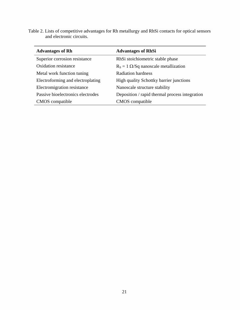
New device concepts deploying rhodium are being emphasized in this paper due to the fact that previous work has shown that the metal and its silicide are advantageous for high reliability in electronic devices and circuits for (1) low Schottky barriers, (2) proven application in bipolar circuits, (3) extensibility to contacting Ge and Ge-Si alloying, (4) high quality

4
metal/semiconductor interface structure, (5) feasibility for silicide source doping, (6) a low cost manufacturable process, and (7) corrosion resistance to wet chemistry.
The unique property of extraordinary corrosion resistance leaves Rh unmatched by competing alternatives for high performance nanotechnology devices and circuits. This is exemplified by the notable resistance of rhodium to attack by hot aqua regia (e.g., it is more robust than platinum). Further, rhodium is employed in highly reliable spark-gap electrodes. These properties favor selecting rhodium for robust and passive electrodes in bio-optoelectronics applications, in which devices contain aqueous electrolyte cells, for sensing and controlling chemical and biological activity. Important applications in these fields, that reach beyond the scope of this paper per se, are electronic arrays for gene expression, chemical assay, and non-embryonic stem cell research.
Rhodium-based film and contact technology merits serious consideration for meeting the critical needs of the semiconductor industry, which is seeking the scaling targets of CMOS devices with tens of nm design rules. Rhodium films can also serve as passivation coatings for electronic devices and interconnects
Rhodium and platinum metal films are deposited by radio-frequency (r.f.) bias sputtering, which is adaptable to ultra-low ion implantation of rhodium, or by electrochemical plating. Rapid thermal processing, a technique that is well established to form silicides in microelectronics fabrication, is used to form low specific resistivity contacts and Schottky barrier junctions.
TECHNOLOGY PATHWAYS
Related development of two optoelectronics technology components, Schottky-barrier contacts and beam leads or air bridges (microbridges), which were originated in silicon microelectronics and subsequently adapted for optoelectronics in compound semiconductors, is described in figure 1. Schottky-barrier contacts were first implemented in silicon circuits comprising bipolar transistors, insulated-gate field-effect transistors (IGFET), photodiodes and phototransistors [10] and are used for making Ohmic contacts to semiconductors [11]. Silicon micromachining methods that were originally developed for beam leads and microbridges [12] became the workhorse for MEMS (micro-electro-mechanical systems). There is now a renaissance in Schottky contacts, particularly for shallow junctions with low parasitic series resistance in advanced CMOS transistors [13,14] that are extensible to BiCMOS circuits with channel mobility enhancements of strained silicon and SiGe alloys. Silicon-based optoelectronics can draw upon the successes of Schottky and beam lead technology in high-speed optoelectronics that were developed in compound semiconductors, such as Schottky-barrier GaAs, InP, and InGaAs detectors, mixers and multipliers, which can now reach THz frequencies [15,16].
Trends since the 1960’s of two key dimensions of contemporaneous state-of-the-art MOS transistors, namely the critical gate length (following scaling of Moore’s law) and the channel depth, are sketched in figure 2. While gate lengths have been dramatically reduced by many orders of magnitude through advances in silicon processing and device design, the channel depth has remained largely unchanged, owing to the physical limitations of inversion layers or the

5
conducting channels (e.g., thin body) in silicon transistors. The fact that these two dimensions have now become comparable to one another is leading to a rethinking of the applicable theories that underlie device scaling and design. Reductions in gate lengths to the tens of nanometers have resulted in increases in the longitudinal component of the electric field to more than 105 V/cm. Thus the relevant metric controlling the performance of transistors is shifting from emphasis on the transport mobility to the high-field saturation drift velocity. The variation of electron transport velocity with electric field is shown in figure 3 for Si, GaAs, and a SiGe (30% Ge) alloy [17,18,19]. Although mobilities (determined from slope) at low fields depend on doping (~ 1017 cm−3 assumed for illustration), they are generally highest for GaAs and lowest for Si, in part because GaAs has a lower effective mass and because mobility scales inversely with effective mass. However, the high-mobility advantage of GaAs [20] over Si becomes largely irrelevant for short channels and in the presence of high electric fields, because the saturation velocities of electrons in the two semiconductors are theoretically comparable (107 cm/s). Thus, in the high-field region silicon, germanium and SiGe alloys provide transport speeds that are comparable to GaAs. The importance of saturation velocity effects has been shown through simulation for heterostructure bipolar transistors with Si1−xGex alloy in the base [21].
A further consideration of high fields in short channel devices is the ability to model the drive current, in which theory of the transport current in terms of a drift-diffusion response to an electric field begins to break down. In this regime, a more fruitful theoretical approach is the one proposed by Landauer, in which current flow is considered in terms of the injection of carriers at the source contact and the probability of their reaching the drain contact [22]. This electron transport concept has been modeled for various MOSFET devices using Monte Carlo simulations [23], which have shown that the maximum drive current depends on the density of states effective mass. This is in contrast to the inverse variation of mobility with drift-diffusion effective mass. In figure 4, transport through two-dimensional short channels in Si, Ge, and a compound semiconductor such as GaAs is illustrated as stochastic flow through pipes in phase space with cross sections scaling with the density of states effective mass. Low density of states in compound semiconductors restricts current throughput, when compared to Si or Ge, leading to lower saturation drive current for short channel transistors. Monte Carlo simulations of electron transport in strained silicon nanoscale MOSFETs find velocity distributions that are statistically distributed about the saturation velocity value and include a ballistic hot carrier component [24].
Silicon-germanium technology has been introduced into high speed CMOS technology to capture increased carrier mobility advantages of strained-layer epitaxy [19,25], which is 46% for n-channel devices and 60 to 80% for p-channel devices [26]. Nanoscale structures are being implemented, for example, by wrap-around gate transistor designs that enable the manufacturability of aggressive high-performance design rules. Commercially viable integration of photoreceiver devices with SiGe CMOS needs to be attentive to compatible materials, thermal budget and processing requirements [27], and in particular to the inherent metastability of strained semiconductor multilayers [28]. Variation of the critical thickness for the epitaxial planar growth of S1−xGex films on silicon as a function of Ge concentration x is shown in figure 5 [29]. Films grown in region A have commensurate epitaxy, where in-plane lattice spacings are equal and the SiGe film is strained. Epitaxial strain is relaxed in region B, permitting epitaxial growth of a strained Si layer on top of the SiGe alloy layer.

6
BEAM LEAD AND MICROBRIDGE (AIR BRIDGE) DEVICES
Beam lead and air bridge technologies have been used to manufacture billions of robust components at extremely low cost [30]. In providing the ultimate low-κ dielectric (κ =1) for integrated circuits, air bridges are now replacing physical media separating interlayer conductors [31] and re-establishing their original purpose. They allow flexibility in the design and assembly of optoelectronics modules by integrating Schottky barrier photo detectors with, e.g., microwave electronics [32]. An example of a beam lead device is the Schottky barrier microwave frequency converter shown in figure 6 [33]. Magnetic self-assembly is another and more recent innovation that provides low cost manufacturing of systems based on beam leaded components and interconnects [34,35]. This technology is an outgrowth of the low cost methods for producing macro assemblies that were developed originally for flat panel displays [36,37]. It is a manufacturing method with extraordinary cost advantages over flip-chip and solder-bump methods of fabricating hybrid modules. Generalizing a published analysis of pricing data trends [38], one could project a unit cost of $3 per photoreceiver module in profitable mass production quantities.
Beam lead technology is used for air-insulated crossovers in integrated circuit interconnections to enable low capacitance, dual dielectrics, high yield, and reliability. Beam-lead crossover methods have been effective for integrated circuit chips as well as complex substrates. Component devices with beam leads are fabricated with the same techniques used in MEMS technology that itself originated with the original beam lead technology [39-43]. Figure 7 shows the cross-section a high-frequency beam-lead switching transistor. The beam leads extend beyond the edges of the silicon device and can be directly connected to the wiring patterns laid down on the substrates. The beam leads are relatively thick (about 10 µm) compared to the active region of the device and associated parts. After forming the device in single-crystal silicon, the leads are deposited and then silicon is etched away, leaving only the beam leads interconnecting the devices and holding them in place. The beam leads provide electrical connections and mechanical support for the semiconductor. This technology simplifies fabrication and assembly procedures for many types of semiconductor devices and circuits, including transistors, diodes, and integrated circuits. The technique, which is ideally suited to couple the advantages of MEMS fabrication of high performance transistors and the magnetic self-assembly, is appropriate for making arrays and modules that integrate Schottky-barrier photo detectors with high-speed SiGe electronic circuitry.
A structure encompassing the beam leads and air isolation is shown in figure 8. In this type of circuit, the components are physically, and therefore electrically, isolated from each other. Beam leads support and interconnect the components. The actual structure illustrated in figure 8 is only 1.3-mm across. This technology has been used to produce billions of versatile and low cost parts of exceptional reliability (e.g., under 1 failure in 109 device hours) in telecommunications electronic switching systems.
Another feature of the beam-lead structure is that silicon (or other semiconductor) wafers may contain either single devices or complete circuit modules that can be directly connected with beam leads. Separate steps for bonding the circuit to the substrate and connecting individual wires are not necessary with beam-lead devices or circuits. Diodes, moderate- and ultrahigh-speed transistors, and ultrahigh-speed logic circuits have been built and tested with this

7
method. Ruggedness of beam-lead devices and circuits were proven by their reliability tests that included thermal ageing at 360 °C in steam and centrifuging to greater than 105 g.
Combined use of beam lead and Schottky barrier technologies, as in the right hand side of the roadmap sketched in figure 1, has proved to be a powerful synergism for high frequency compound semiconductors devices. Several examples of such Schottky diodes are briefly mentioned here. Schottky-barrier beam lead detectors implemented in GaAs are in commercial production [16]. Figure 9 shows cross section detail of a GaAs Schottky barrier detector [44]. High performance optoelectronics based in silicon offer opportunities for realizing very low cost of manufacture with military level of reliability. Schottky barriers in silicon-based semiconductors are reviewed in the next section.
SCHOTTKY BARRIER DETECTORS
Schottky barrier photo detector technology is based on the principle of thermionic emission of photo-excited electrons generated in the metallic film near the semiconductor interface over the Schottky barrier and subsequently collected in the semiconductor. In the pioneering work of Andrews and Lepselter, it was shown that the thermionic emission currents for high quality Schottky barriers with PtSi and RhSi films on n-type Si experimentally obey the Richardson-Dushman equation with a Richardson factor, A** = 112 A cm-2 K-2, a value that agrees with the calculated value for Si [5]. Ideality factors under forward bias current, n = 1.02, indicate high quality barriers. Reverse bias current-voltage data for RhSi/n-Si and PtSi/n-Si Schottky diodes are in nearly perfect agreement with theory, after taking into account known guard-ring effects at high bias. Depletion layer recombination is negligible in these junctions. Schottky barrier heights, φB, and reverse bias saturation current densities, Jsat, for RhSi and PtSi Schottky contacts on n- and p-type silicon are compared in Table 1. The data show that the dark current of a RhSi / p-Si detector will be lower than that of a PtSi / p-Si detector by a factor of 200/8 = 25. Previous work and reference data for various metal silicides has been compiled by Murarka [45] and by Rhoderick and Williams [46].
Photoemitted carriers are collected for photon energies that exceed the Schottky barrier height. The cut off wavelength, λc, is related to the barrier height by the relation λc = [1.2399 µm/eV] / φB. While the barrier height is theoretically determined by the difference between the metal work function and the semiconductor electron affinity (4.05 eV for Si and 4.0 eV for Ge), it is in practice determined by the presence of Bardeen interface states. The effective barrier height is also reduced by quantum wave function effects, the image potential and the electric field at the interface. Interface electric field effects are used to tailor the barrier height for optimizing the tradeoff between photon collection efficiency and dark current. These and other methods may be used to improve device performance.
RhSi and PtSi each form Schottky barriers with high quality interface structure. Note that the sum of the barrier heights listed in Table 1 approaches the theoretical value of the band gap of Si (1.12 eV) in accord with device fundamentals. The properties of PtSi/Si are somewhat better characterized, although the properties of RhSi are similar. PtSi has B31 orthorhombic crystal structure and a high density of electron states at the Fermi level, which produces low electrical resistivity of 35 µΩ cm, a short Thomas-Fermi screening length of 0.06 nm, and even superconductivity at low temperatures (Tc ~ 0.5K). RhSi forms a cubic crystal structure [47] and

8
has similarly low resistivity. The low resistivity is exploited to produce devices with low parasitic resistance and thus high operating frequency. Since the charge screening distance is much shorter than the spacing between Si and silicide lattice planes at the interface, the electronic metal-semiconductor interface is especially abrupt. Thus electron wave functions are insensitive to bulk lattice defects in the silicide.
The Schottky barrier height for RhSi / p-Si is 0.33 ± 0.01 eV as obtained from the temperature dependence of the experimental I-V characteristics nearly perfectly matches theory. This corresponds to λc = 3.8 µm, which is ideally suited for designing sensors that operate at 2 µm. The barrier height may be reduced by a built-in electric field produced by shallow ion implantation and rapid thermal annealing (“spike” dopant). Figure 10 shows the theoretical calculation for the barrier lowering as a function of the activated implant dose. A shallow activated donor implant of 5×1012 cm−2 lowers the barrier height by 0.1 eV.
When a layer of SiGe alloy is inserted between PtSi or Pd2Si and Si in an SBD structure of the form PtSi/Si1−xGex/Si, the Schottky barrier height may be controlled with Ge concentration, x, (previously studied for x up to 0.2 and p type semiconductor) as well as by reverse bias voltage [48,49]. Barrier height modifications for PtSi on n-type PtSi on n-type Si1−xGex are plotted in figure 11. Although results have not been reported for Schottky barriers formed as a junction of a ternary metallic compound comprising a platinum-group metal, silicon and germanium that is in direct contact with a silicon-germanium alloy semiconductor, it is a logical extension of the class of materials that could be readily integrated with high-performance SiGe circuits. Of particular interest are the ternary metal-alloy Schottky-barrier junction devices, RhSi1−yGey/Si1−xGex and PtSi1−yGey/Si1−xGex. Theoretically, one may expect that the properties of junctions involving ternaries would be similar to those of the binaries (figures 10 and 11). Ternary compound junctions formed from Rh and Pt are expected to follow a similar process technology. Device examples presented in this paper are based on rhodium because of its technical advantages, as discussed below. The rationale for favoring a Schottky barrier technology that is based on rhodium are described in Table 2.
RhSi/n-Si photo detectors operating at 40 Gb/s can already be manufactured by proven mass production integrated circuit methods with non-aggressive lithography and patterning steps. The method of choice for low-cost fabrication of thin silicide films is r.f. sputtering and thermal annealing. Conventional ion implantation and rapid thermal annealing are further options for optimizing the Schottky barrier height and profile with respect to maximizing quantum efficiency, minimizing dark current, and suppressing noise background.
The Schottky barrier height for RhSi/n-Si is 0.69 ± 0.01 eV, which corresponds to λc = 1.8 µm, and which is ideally suited for the design of photoreceivers operating at 1.5 µm. Devices based on PtSi/n-Si Schottky barriers can be operated at 1.3 µm. The barrier height may be reduced by the combination of reverse bias field and a built-in electric field produced by shallow ion implantation and rapid thermal annealing (figure 10). A shallow activated donor implant of 2×1012 cm−2 and 2 V reverse bias device operation lowers the barrier height for operation at 1.3 µm. Theoretically, one expects a similar effect of doping for Rh based contacts and for the ternaries, RhSi1−yGey / Si1−xGex and Pt Si1−yGey / Si1−xGex. Semiconductor type (n or p) and doping concentrations are selected for the Si1−xGex system based on specific applications.
9
SCHOTTKY JUNCTION FORMATION
Formation of RhSi / Si contacts uses a method that circumvents potential manufacturing issues in silicide-germanide formation, whereby barrier height and interface state densities could have variable dependence on surface preparation and cleaning. Manufacturability requires production of Schottky barrier junctions with near ideal I-V characteristics and tight tolerances on the barrier height. This is achieved using ultra-low energy (150 eV) plasma immersion ion implantation, which is implemented as biased r.f. sputtering. The processing apparatus is illustrated in figure 12. The sputtering chamber is filled with low-pressure argon. This system allows a preliminary sputter clean step by bombardment with Ar ions. The frequency of the r.f. power supply is selected so that the period of oscillation is approximately twice the transit time for Ar ions to drift between the Pt or Rh cathode No. 2 and the silicon substrate. The current flowing in the plasma during each half cycle is carried alternately by electrons and Ar ions. For Rh sputter deposition, the bias potentials are set as shown in figure 12. Experiments with silicide films show that the RhSi reaction is formed by annealing at 600 °C or with a low thermal budget rapid thermal annealing (RTA) technique. Unreacted Rh is removed by back sputtering, i.e., plasma etching, without significantly attacking the RhSi film. This leads to an RhSi/Si junction with near optimum metal-semiconductor interface.
The interface corresponding to the Schottky junction is therefore buried, formed in clean semiconductor alloy, and well below surface contaminant layers that may arise from the fabrication processing residues. Silicide or silicide-germanide formation and dry sputter etch steps are readily implemented as separate process modules. The ultra-low energy ion implantation by this technique is superior to other methods of forming silicide contacts. The RhSi material is expected to have a defect density sufficiently low so that the electron mean free path exceeds the photon penetration depth, allowing for efficient internal photoemission in the Schottky detector.
Furnace growth kinetics of RhSi formed from conventional physical deposition of rhodium indicate parasitic reactions between the silicon substrate and trace oxygen contamination in the annealing ambient, as evidenced by degradation of the resistivity of the RhSi film [50], deviations from ideality of the RhSi/Si Schottky junctions [7], and the need to resort to ion-beam mixing techniques [8]. The Schottky barrier height of the nearly ideal junction formed from plasma deposition is compared with those from conventional methods in figure 13. While barrier heights obtained by furnace annealing approach the ideal limit, one notes a non-monotonic variation of Schottky barrier height with anneal temperature, which is indicative of intermediate interfacial reactions. High quality junction formation requires suppression of parasitic oxidation, which can be achieved by vacuum annealing [5].
Since rapid thermal processing (RTP) has been advantageously utilized in silicon microelectronics processing [27], it would provide a silicide-germanide formation process that is reproducible and suitable for manufacture. The advantage of RTP is realized when the desirable process of metal-silicide-germanide formation is governed by effective activation energy that is higher than that of the undesirable growth of SiO2 in grain boundaries and at the contact interface. Since RTP is currently being used to manufacture silicides in silicon integrated electronics, extension to rhodium is likely to realize similar success.

10
Previous work used the plasma sputtering method to fabricate RhSi and PtSi Schottky-barrier diodes of nearly ideal I-V characteristics for various circuit applications. For example, low-power bipolar transistor memory cells were developed with high barrier, RhSi/n-Si, and low barrier, RhSi/p-Si, Schottky diodes. Figures 14 (a) and 14 (b) show the operational current-voltage (I-V) characteristics for the n and p type Schottky diodes in the circuit. The low barrier diodes in the circuit serve as current limiting non-linear elements in the circuit, a feat that is not achievable with linear current limiting resistors. Figure 14(c) shows that the Schottky barrier theory with image force and static corrections for the low-barrier RhSi/p-Si diode is in agreement with experimental reverse-bias data [5].
Another application is the use of Schottky contacts in MOS transistors. They were first used to make very shallow, sharp emitter profiles in bipolar transistors. Figure 15 illustrates a novel device concept introduced in this paper. It shows the cross section view of a Ag/RhSi/Si thin-film structure for the source and drain contacts. The notable attribute of this structure is that a low resistance film of approximately 25 nm of thickness can be formed that closely matches the depth of the silicon inversion layer in a low-voltage MOS transistor. Moreover, it is lateral scale independent. This technique circumvents the problem of forming ultra shallow doping layers with low link up resistance for high-speed CMOS technology, thus eliminating the need to thwart transient diffusion of shallow implanted dopants by laser or flash-lamp annealing. It is therefore a viable solution for minimizing the linkup series resistance between contact junction and channel. Low series resistance is achieved by a low sheet resistance of Rs ≈ 1 Ω/square for the Ag/RhSi bilayer. The thin Ag film can be deposited over the contact, which acts as a diffusion barrier, by self-aligned chemical deposition. Low contact resistance is achieved with Ohmic RhSi/n++-Si or RhSi/p++-Si contacts. An ultrashallow Rh implant in the gate metallization at the dielectric interface is used to modify the work function of the gate metal and thereby tune the threshold voltage of the MOSFET.
Figure 16 shows the dual gate application of Schottky barrier contacts that was recently proposed and modeled theoretically [50]. The conducting channel is formed as an ultrathin (25 nm) silicon body with silicon-on-insulator (SOI) technology. Simulation studies suggest that Schottky source and drain offer significant performance improvement over doped source and drain. A Schottky barrier CMOS FinFET comprising a sub-gate structure for forward-biasing PtSi contacts was recently fabricated and shown to be viable for low leakage and high drive current and thus be able to realize the requisite high performance [51].
SCHOTTKY OPTOELECTRONIC DEVICES
Schottky barrier detectors usually produce a lower quantum yield than p-n junction detectors, but that disadvantage can be addressed by various techniques to boost photon capture efficiency. Among these are adaptations of design concepts used for solar cells [52]. One method is to apply facet texturing the optical input port in combination with an antireflection (AR) coating. The facets create total internal reflection of most of the photons, which are reflected from the metal-semiconductor interface, owing to the large index of refraction of the semiconductor, relative to that of the AR coating. Texture is also used at the metal-semiconductor interface to enhance both photon capture and the effective solid angle for thermionic emission of electrons photo excited in the metal. A texturing technique has been used

11
to boost the quantum efficiency of PtSi/Si SBDs to above the theoretical maximum [53]. Texturing methods include modified porous silicon etching, growth of Si1−xGex islanded films overcoated with Si, and pulsed laser chemical etching. Implementing the structure in silicon on insulator (SOI) is also a way to increase effective photon capture. Distributed Bragg reflectors containing alternating multilayer films of Si and SiO2 with at least two periods have been shown to be suitable for making back reflectors with near unity reflectivity [54].
A novel approach to photon trapping that is introduced in this paper is the SBD structure shown in figures 17 (a) and 17 (b). A Schottky contact metal film is formed on the inner surfaces of a blind hole etched into the silicon crystal. Protective antireflective cover layers are included, but not shown for clarity. Light trapping for photons of wavelength λ is optimized by arraying blind holes of diameter λ/2 spaced a distance λ apart. Since the holes function as the fundamental mode light guide whose walls are weakly absorptive, all of the photons are essentially captured by the metal film (e.g., RhSi). Photons entering in the Si material between the holes are guided into the Si crystal by multiple reflections at the wall interfaces (owing to index of refraction discontinuity) and are absorbed by the RhSi film. The geometry is thus optimized for capturing most of the photons incident on the sensor. For a p-type device, photo excitation of electrons above the Fermi level in the metal induce free carrier holes in the silicon crystal, which are swept by a small bias potential (0.1 V) towards the p+ collector contacts. This recessed SBD uses a method that is more effective than simple random or periodic surface texturing. It is also defined by a controlled and manufacturable process unlike many previously proposed methods. Preliminary analysis indicates that the ideal depth of the holes is about three times the diameter. This allows sufficient photon trapping without an excessive increase in the dark current.
A plan view of an array of photon traps is illustrated in figure 17 (b). The emitter and collector electrodes of individual hole elements are strapped together in crossed parallel lines. The collector electrodes and lines are embedded in the crystalline silicon and are insulated from the metallic emitter lines by the oxide. An individual pixel can comprise a single hole or an array of holes, the number depending on the focal plane optics. For example, a pixel comprising a 3 × 3 array of holes, as indicated in figure 17 (b), would be coupled by crossed emitter and collector lines. Read out in the focal plane array of such pixels could use standard charge coupled signal transfer. In a typical RhSi /p-Si device, the doping of the p− semiconductor under the contact would be 1017 cm−3. Holes are collected in the collector contact, in which the p+ doping is 2 × 1019 cm−3 and the thickness is 0.8 µm. The p+ layer is largely transparent to the incident photons. The one-pass attenuation is only 0.05 dBm. For a conservative 25% photon capture efficiency, this RhSi SBD sensor has an estimated internal quantum efficiency of 10% and responsivity of 0.16 A/W. Trilayer Ti/Pt/Au is used for metallization interconnect because it is very robust, has zero electromigration, and keeps parasitic series sheet resistances below 2 Ω/Sq, which is required for high-speed performance.
An adaptation of the recessed SBD concept can be implemented with RhSi/Si Schottky diodes in radiation hardened focal plane arrays. The RhSi contacts are formed in holes etched in silicon using current techniques for forming deep vias for 3D interconnect technology. The desired aspect ratio of about 3:1 and hole diameter of 2 µm for operation in the infrared are readily achieved. The holes are prepped with a seed layer deposited by electrochemical means, such as a thin Pd film that is electroless deposited on hydrophilic prepared silicon.

12
Gain with Schottky barrier junctions can be significantly improved with avalanche diodes [55] and phototransistors, which were an early proposal by Shockley [56]. The advantages of choosing phototransistors over avalanche photodiodes include better current gain and lower noise.
Optical response in the traditional bipolar phototransistor is controlled by irradiation of the base-to-collector junction. While ordinary bipolar and MOS transistors are photo sensitive, the bipolar phototransistor is optimized for photon collection by giving the base and collector larger areas. Owing to the current gain of the transistor, the responsivity of the phototransistor exceeds that of photodiodes. A Darlington-pair configuration can be used with a phototransistor as the input transistor. Phototransistors have a dark current arising from the ambient thermally-excited carriers. In a bipolar phototransistor light entering the base region generates electron-hole pairs in the reverse biased base-collector junction and they drift under the influence of the electric field. This produces base current that is injected into the emitter.
The Schottky phototransistor concept proposed in this paper is that of the floating base type. The Schottky barrier contact is on the collector and the base is formed in silicon. Figure 18 shows the circuit for such a p-n-p Schottky phototransistor. A base connection is not used, since the base potential is auto-biased by the photo-generated current at the Schottky junction. The bias condition is therefore implemented rather simply. The collector of a p-n-p transistor is made negative with respect to the emitter (or positive for an n-p-n transistor). In a p-type device positive bias on the Schottky base contact forces photo excited holes that are created at the Schottky barrier into the base with sub-µs residence time in the collector. Similar Schottky contact methods were used to produce log-linear amplifiers with a remarkable 9 decade dynamic range. High speed response is assured by a thin base layer while the responsivity is increased by β ≈ 110 for high current output and low bit error rate signal processing. Device scale allows for 20-Ω circuit series resistance and 30-fF depletion layer capacitance for a monolithic high speed photo detector. The technology extension envisioned is a low inductance, air isolated integrated circuit that is totally integrated with the phototransistor and amplifier.
The Schottky phototransistor is a low-voltage device that can be of the vertical back illumination type. Using air bridges and bonding via beam leads, phototransistors can be integrated with coplanar wave guide SiGe CMOS circuit demodulators to produce monolithic photoreceivers. Modules are mounted with the device sides of the beam-leaded chips facing the substrate. This enables rapid product prototyping of phototransistor sub components independent of circuit integration.
Owing to the physical reciprocity between detection and emission of photons, a SBD that combines the above concepts of light trapping and phototransistor gain may be adapted as a source of light emission from silicon, although the photons would not be generated conventionally as an interband transition in the semiconductor. Validity of the reciprocity principle was demonstrated for high efficiency p-n junction solar cells, in which significant light emission was determined [57].

13
DISCUSSION
Formation of RhSi1−yGey / Si1−xGex contacts (and similarly for Pt Si1−yGey / Si1−xGex) uses a method that circumvents potential manufacturing issues in silicide-germanide formation, especially if surface cleaning preparation is insufficient for reproducible barrier heights and interface state densities. Manufacturability requires production of Schottky barrier junctions with near ideal I-V characteristics and tight tolerances on the barrier height. This is achieved using ultra-low energy (150 eV) plasma immersion ion implantation that is implemented as biased r.f. sputtering.
The operating wavelength range of Schottky barrier detectors can be tailored with greater flexibility than for semiconductor p-n junction devices because the desired Schottky barrier height, φB, is selectable. The available methods include:
1. Selection of Pt or Rh as a metallic constituent of the silicide-germanide.
2. Ge fraction, x, in Si1−xGex.
3. Doping type of the Si1−xGex semiconductor.
4. Doping concentration of Si1−xGex at the interface (analogous to method illustrated in Fig. 10), yielding φB lowering with n-type or raising with p-type.
Schottky barrier heights for PtSi on n-type SiGe alloys can be estimated by scaling the change in barrier height with Ge concentration previously reported for PtSi on p-type strained SiGe alloy layers [47]. There is a need for further experimental verification and study in this direction.
Schottky-barrier detectors in coplanar wave guide circuits can be stand-alone high-frequency devices. These are beam leaded microstrip devices, in which the beam leads are used to make contact to the diode electrodes and are tapered to match, for example, beam lead microwave electronics [31,58,59]. Bonding with beam leads and air bridges has the advantages of being both rugged and inexpensive. A Schottky-barrier photoreceiver that is integrated to a microwave strip line center conductor would be like microwave detectors [9] and can be built in insulating Si1−xGex on a Si or SOI substrate. In a diode or phototransistor detector using photon generation at a Schottky RhSi1−yGey/n-Si1−xGex contact, the doping of the Si1−xGex region under the contact is on the order of n− ~ 1017 cm−3 and has a thickness on the order of 0.1 µm. Electrons are collected in a RhSi1−yGey/n+Si1−xGex contact, where the n+ layer has a doping of 2 × 1019 cm−3 and thickness of 0.8 µm, which gives a sheet resistance Rs = 30 Ω/Sq. This would be suitable for detecting 1550 nm photons, since the n+ layer is largely transparent to 1550 nm photons. The one-pass attenuation is only 0.05 dBm. For a conservative 25% photon capture efficiency, such a Schottky RhSi1−yGey/n-Si1−xGex detector has an estimated internal quantum efficiency of 2% and responsivity of 20 mA/W.
Extending Schottky-barrier imaging sensor technology to advanced high-speed devices with planar contacts in an interdigitated or concentric layout could fully exploit the high saturation drift velocity of electrons in the depletion layer (up to 107 cm/s). The theoretical limit on bit rate in digital devices is on the order of 40 Gb/s [60]. This geometry circumvents any need for an n+
14
layer in the photon pathway and its parasitic series resistance. Moreover, with diode technology based on Rh (or Pt), the detector speed can be optimized absolutely, unlike semiconductor p-n junction devices, in which depletion layer thickness dictates photon generation efficiency. High device speed is realized in this approach because of the 1-ps electron transit time in the depletion layer field in n− Si1−xGex under RhSi1−yGey/n-Si1−xGex contacts in the diode. Signal to thermal emission noise ratio of 40 is achieved with an optical input power of −20 dBm. This device would use Ti/Pt/Au metalization for high-speed performance.
The RhSi1−yGey/ Si1−xGex Schottky barrier is a natural substructure for a SiGe heterostructure bipolar phototransistor of the floating base type for a monolithic high speed photo detector. The Schottky barrier contact is on the collector and the base is formed in Si1−xGex. For an n-type device, negative bias on the RhSi1−yGey contact forces photo excited electrons that penetrate the Schottky barrier in to the base with sub-ps residence time in the collector. For extending the technology to optical communications devices, a beam lead method is used to a produce a low inductance, air isolated integrated circuit that is totally integrated with the phototransistor and amplifier.
High framing rate, long wavelength infrared cameras (beyond 5 microns) with Schottky-barrier diode arrays may function in the thermal emissive mode. One such utilitzation is the all solid state temperature sensor that is based on the physical principle of thermionic emission [61]. The temperature sensor comprises a pair of Schottky-barrier diodes of dissimilar Schottky barrier heights. The differential thermionic emission current is converted to a voltage that is used in a temperature control feedback loop. The semiconductor circuit is formed on a thin, low thermal conductivity membrane [62]. It is constructed with beam lead technology and formed with selective etching (like MEMS methods). The passive element, which serves as a thermal radiation sensor element is integrated with active elements in close proximity. Although it is used as an infrared bolometric sensor, it has a very fast response time, owing to the low mass and low thermal heat sinking of the passive pattern.
Schottky barriers can be formed by ultra-low energy ion implantation of Pt or Rh films on Si prepared with a deposited Si1−xGex film with islanded growth morphology (Stransky-Krastanov growth mode) [29,63,64]. The deposition conditions for the growth of this nanoscale texture is energetically driven by the strain caused by lattice mismatch between the Si1−xGex phase and the Si substrate that gives rise to positive wetting angle of the SiGe islands on Si. The lattice mismatch strain is shared by local relaxation of the Si substrate below the Si1−xGex islands. The Si1−xGex is in compression while the Si underneath is in dilation. Although the conduction band in cubic Si is 0.020 eV higher than the conduction band in strained Si1−xGex, the strain in the Si at the interface is likely to eliminate this small barrier [65]. The islanded film can be subsequently capped with a sacrificial Si film layer that is consumed in the metal silicidation reaction [47]. A 10 nm Rh layer and a 14 nm Si cap will produce a RhSi film of approximately 20 nm thickness. The nanostructured interface between the RhSi film and the semiconductor substrate serves several purposes. Collection efficiency of photo excited electrons is increased. This is analogous to other methods of enhancing the quantum efficiency of Schottky-barrier photodetectors, such as found by porous silicon formation [53]. Reduction of the barrier height increases thermionic emission of photo excited electrons into the semiconductor. The method can be extended to form RhSi1−yGey/ Si1−xGex contacts, where y ≤ x.
15
CONCLUSIONS
This work presents several new silicide-germanide high performance optoelectronic materials and devices based on the platinum group metals of Pt or Rh, drawing particular attention to the unique properties of Rh. Applications include (1) robust low-resistance Schottky contacts to highly doped source and drain in MOS transistors, (2) Schottky-barrier source field-effect transistors for high speed, low power applications, (3) high speed infrared detection by internal photoemission in Schottky barrier junctions in super-beta high-gain phototransistors, (4) ultrathin interfacial films for work function modification and tuning in metal-gate high-κ MOS transistors, (5) bolometric infrared detectors, and (6) low sheet resistance metallization. New device concepts are introduced for photon trapping in a re-entrant Schottky-barrier detector, dual-layer Ag-RhSi Schottky contacts for MOS transistors, and floating-base auto-biased phototransistors.
ACKNOWLEDGEMENTS
The authors dedicate this paper to the memory of the late Walter F. Kosonocky, acknowledging his pioneering work in the field of infrared imaging. This work was supported in part by BTL Fellows, Inc., New Jersey Institute of Technology, and The Minerals, Metals and Materials Society.

16
REFERENCES
1. W. F. Kosonocky, Review of Schottky-Barrier Imager Technology, SPIE Advent Technologies Series, Vol. AT 2: Current Overviews in Optical Science and Engineering II, edited by Richard Feinberg (SPIE, 1990), p. 470.
2. W. F. Kosonocky, M. B. Kaplinsky, N. J. McCaffrey, J. Li, H. Martynov, E. Hou, N. M. Ravindra, C. N. Manikopoulos, S. Belikov, F. M. Tong, and V. Patel, Multi-Wavelength Imaging Pyrometer (M-WIP) for Semiconductor Process Monitoring and Control, Wright Laboratory Final Report for 08/24/92 – 12/31/94, Wl/MTEM WPAFB OH 45433-7739 (U.S. Dept. of Defense, Feb., 1995).
3. K. Solt, H. Melchior, U. Kroth, P. Kuschnerus, V. Persch, H. Rabus, M. Richter and G. Ulm, Appl. Phys. Lett. 69, 3662 (1996).
4. D. Wilson, Bell Telephone Laboratories, Whippany, N.J. (1968), unpublished.
5. J. M. Andrews and M. P. Lepselter, Solid State Electronics 13, 1011 (1970).
6. D. A. Hodges, M. P. Lepselter, D. J. Lynes, R. W. MacDonald, A. U. Macrae, and H. A. Waggener, IEEE J. Solid-State Circuits SC-4, 280 (1969).
7. D. J. Coe, E. H. Rhoderick, P. H. Gerzon, and A. W. Tinsley, Inst. Phys. Conf. Ser. (London) 22, 74 (1974).
8. E. P. Burte and G. Neuner, J. Appl. Surf. Sci. 53, 283 (1991).
9. Y. Wu, B. M. Armstrong, H. S. Gamble, Z. Hu, Q. Chen, S. Yang, V. F. Fusco, and J. A. Carson Stewart, IEEE Trans. Microwave Theory and Techniques 46, 641 (1998).
10. S. M. Sze, Physics of Semiconductor Devices, 2nd Edition (John Wiley & Sons, New York, 1981).
11. M. P. Lepselter and J. M. Andrews, in Ohmic Contacts to Semiconductors, edited by B. Schwartz (Electrochem. Soc., Princeton, N.J., 1969), p.159; M. P. Lepselter and S. M. Sze, U.S. Patent 4,343,082, Method of Making Contact Electrodes to Silicon Gate, and Source and Drain Regions of a Semiconductor Device (Aug. 10, 1982); RE 32,613 (Feb. 23, 1988).
12. M P. Lepselter, H. A. Waggener, R. W. MacDonald, and R. E. Davis, Proc. of the IEEE 53, 405 (1965); M. P. Lepselter, Bell Laboratories Record 44, 298 (1966); M. P. Lepselter, Bell System Tech. Journal 45, 233 (1966).
13. C. Wang, J. P. Snyder, and J. R. Tucker, Appl. Phys. Lett. 74, 1174 (1999).
14. R. A. Vega, Schottky Field Effect Transistors and Schottky CMOS Circuitry, Thesis, Rochester Institute of Technology (Rochester, N.Y. 2006).
15. F. Maiwald, F. Lewen, B. Vowinkel, W. Jabs, D. G. Paveljev, M. Winnewisser, and G. Winnewisser, IEEE Microwave and Guided Wave Lett. 9, 198 (1999).
16. R. W. McMillan, Terahertz Imaging, Millimeter-wave Radar, (U.S. Army Space and Missile Defense Command, Huntsville, Alabama, 2005), http://www.nato-asi.org/sensors2005/papers/mcmillan.pdf.
17
17. D. M. Caughey and R. E. Thomas, Proc. IEEE 55, 2192 (1967).
18. K. Ismail, S. F. Nelson, J. O. Chu, and B. S. Meyerson, Appl. Phys. Lett. 63, 660 (1993).
19. P. Dollfus, J. Appl. Phys. 82, 3911 (1997).
20. M. S. Shur, IEEE Electron Device Lett. 23, 511 (2002).
21. P. L. Cottrell, IEEE Electron Device Lett. 11, 431 (1990).
22. Y. Imry and R. Landauer, Rev. Mod. Phys. 71 S306 (1999).
23. M. V. Fischetti, S. E. Laux, P. M. Solomon, and A. Kumar, J. Computational Electronics 3, 287 (2004).
24. V. Aubry-Fortuna, A. Bournel, P. Dollfus and S. Galdin-Retailleau, Semicond. Sci. Technol. 21, 422 (2006).
25. F. M. Bufler, P. Graf, S. Keith, and B. Meinerzhagen, Appl. Phys. Lett. 70, 2144 (1997).
26. D. A. Antoniadis, I. Aberg, C. NíChléirigh, O. M. Nayfeh, A. Khakifirooz, J. L. Hoyt, IBM J. Res. & Dev. 50, 363 (2006).
27. A. T. Fiory, J. of Materials 57, 21 (2005).
28. A. T. Fiory, J. C. Bean, R. Hull, and S. Nakahara, Phys. Rev. B 31, 4063 (1985).
29. J. C. Bean, T. T. Sheng, L. C. Feldman, A. T. Fiory, and R. T. Lynch, Appl. Phys. Lett. 44, 102 (1984); A. T. Fiory, J. C. Bean, L. C. Feldman, I. K. Robinson, J. Appl. Phys. 56, 1227 (1984).
30. M. P. Lepselter, in Solid State Technology Magazine, July, 1976 cover story.
31. IBM Borrows Process From Nature to Build Next-Gen Computer Chips, IT News Online, (State University of New York, Albany, N.Y., May 3, 2007), http://www.albanynanotech.org/News/index.cfm?InstanceID=572&step=show_detail&NewsID=600.
32. T.C. Edwards, Foundations for Microstrip Circuit Design, John Wiley & Sons, New York (1981).
33. M. V. Schneider, U.S. Patent No. 3,882,396 (May 6, 1975).
34. Martin P. Lepselter, Flat Panel Display Having Magnetic Elements, U.S Patent No. 5,962,975 (October 5, 1999).
35. M. P. Lepselter, Flat Panel Display Having Conductors Magnetically Bonded to Substrate, U. S. Patent Application No. 20040227463, (Nov. 18, 2004).
36. M. P. Lepselter, Gas Discharge Panel Display and Method for Making the Same, U.S. Patent 5,469,021 (Nov. 21, 1995).
37. M. P. Lepselter, Pressurized Plasma Display, U.S. Patent No. 5,990,620 (Nov. 23, 1999).
38. M. P. Lepselter and S. M. Sze, DRAM Pricing Trends – The Pi Rule, IEEE Circuits and Devices Magazine (Jan., 1985), pp. 53-54
18
39. M P. Lepselter, H. A. Waggener, R. W. MacDonald, and R. E. Davis, Proceedings of the IEEE 53, 405 (1965).
40. M. P. Lepselter, Bell Laboratories Record 44, 298 (1966).
41. M. P. Lepselter, Bell System Tech. Journal 45, 233 (1966).
42. M. P. Lepselter, Bell System Tech. Journal 47, 269 (1968).
43. M. P. Lepselter, Method for Making Closely Spaced Conductive Layers, U.S. Patent No. 3,461,524 (Aug. 19, 1969).
44. T. Asano, K. Onada, Y. Nakajima, S. Murai, H. Tominaga, K. Hirata, M. Sakakibara, and H. Ishihara, Schottky Barrier Diode, U. S. Patent No. 6,627,967 (Sep. 30, 2002).
45. S. P. Murarka, Silicides for VLSI Applications (Academic Press, New York, 1983).
46. E. H. Rhoderick and R. H. Williams, Metal-Semiconductor Contacts, 2nd Edition (Clarendon Press, Oxford 1988).
47. S. Geller and E. A. Wood, Acta Cryst. 7, 441 (1954).
48. X. Xiao, J. C. Sturm, S. R. Parihar, S. A. Lyon, D. Meyerhofer, S. Palfrey, and F. V. Shallcross, IEEE Electron Device Lett. 14, 199 (1993).
49. J. R. Jimenez, X. Xiao, J. C. Sturm, and P. W. Pellegrini, Appl. Phys. Lett. 67, 506 (1996).
50. P. A. Psaras, R. D. Thompson, S. R. Herd, and K. N. Tu, J. Appl. Phys. 55, 3536 (1984).
51. D. Connelly, C. Faulkner, and D. E. Grupp, IEEE Trans. Electron Devices 50, 1340 (2003).
52. H.-C. Lin, M.-F. Wang, F.-J. Hou, H.-N. Lin, C.-Y. Lu, J.-T. Liu, and T.-Y. Huang, IEEE Electron Device Lett. 24, 102 (2003).
53. A. T. Fiory and N. M. Ravindra, J. Electron. Materials 92, 1043 (2003).
54. F. Raissi, IEEE Trans. Electron Devices 50, 1134 (2003).
55. M. K. Emsley, O. Dosunmu, and M. S. Önlü, IEEE J. Selected Topics Quantum Electronics 8, 948 (2002).
56. H. Melchior, A. R. Hartman, D. P. Schinke, and T. E. Seidel, Bell System Tech. Journal 57, 1791 (1978).
57. W. Shockley, M. Sparks and G. K. Teal., Phys Rev 83, 151 (1951).
58. J. Zhao, M. A. Green, and A. Wang, J. Appl. Phys. 92, 2977 (2002).
59. L. Vegni, A. Toscano and F. Bilotti, IEEE Trans. Microwave Theory and Techniques 49, 970 (2001).
60. H. J. De Los Santos and R. J. Richards, MEMS for RF Microwave Wireless Applications - The Next Wave: Part II, in Microwave Journal, July, 2001.
61. E. Chen and S. Y. Chou, Appl. Phys. Lett. 70, 753 (1997).
62. J. M. Andrews and M. P. Lepselter, Solid State Temperature Sensor Employing a Pair of Dissimilar Schottky-Barrier Diodes, U. S. Patent No. 3,719,797 (March 6, 1973).

19
63. M. P. Lepselter, Semiconductor Integrated Circuitry with Improved Isolation between Active and Passive Elements, U. S. Patent No. 3,411,048 (Nov. 12, 1968).
64. Germanium Silicon: Physics and Materials, in Semiconductors and Semimetals, Vol. 56, edited by R. Hull and J. C. Bean (Academic Press, London 1999).
65. S. C. Jain, Germanium-Silicon Strained Layers and Heterostructures (Academic Press, London, 1994).
66. R. People and J. C. Bean, Appl. Phys. Lett. 48, 538 (1986).

20
Table 1. Schottky barrier heights φB (eV) and reverse bias saturation current densities Jsat (A/cm2) for RhSi and PtSi on p- and n-type silicon.
Silicide φB n-Si
φB p-Si
Jsat p-Si
Jsat n-Si
RhSi 0.69 0.34 8 2−4×10⁻⁵
PtSi 0.84 0.26 200 3−6×10⁻⁷
21
Table 2. Lists of competitive advantages for Rh metallurgy and RhSi contacts for optical sensors and electronic circuits.
Advantages of Rh Advantages of RhSi
Superior corrosion resistance RhSi stoichiometric stable phase Oxidation resistance RS = 1 Ω/Sq nanoscale metallization Metal work function tuning Radiation hardness Electroforming and electroplating High quality Schottky barrier junctions Electromigration resistance Nanoscale structure stability Passive bioelectronics electrodes Deposition / rapid thermal process integration CMOS compatible CMOS compatible

22
Figure Captions
Figure 1. Development pathways for optical and electronic technology components, Schottky barrier contacts and beam leads, in silicon-based and compound semiconductors.
Figure 2. Scaling trends since the 1960’s in channel length (solid curve) and depth (dashed curve) of MOSFET transistors.
Figure 3. Drift velocity vs electric field for three semiconductors. Figure 4. Current throughput as constrained by semiconductor density of states (illustration for
short two-dimensional channels).
Figure 5. Critical thickness of growth of Si1−xGex films on Si. Curve divides the commensurately strained region, A, and strain relaxed region, B.
Figure 6. Beam lead Schottky barrier strip line microwave converter (adapted from Ref. 33). Figure 7. Cut away cross sectional view of high frequency bipolar transistor fabricated with
beam lead technology. Figure 8. Beam-lead, sealed junction circuits fabricated with air isolation. Figure 9. Schematic cross section of a GaAs Schottky barrier detector (adapted from Ref. 44). Figure 10. Theoretical Schottky barrier height lowering with a spike donor implant in Si near the
silicide-Si interface.
Figure 11. Calculated variation of Schottky barrier height at 2 V reverse bias for PtSi/n-Si1−xGex. Figure 12. Apparatus for dual cathode plasma sputtering metal film deposition and ultra-low
energy metal-ion implantation in Si-based substrates. Figure 13. Schottky barrier heights of RhSi/n-Si junctions formed by furnace anneal of Rh
deposited on crystalline silicon. Diamond points are conventional deposition and anneals [46]. Round symbol is the close to ideal result obtained with rf-biased Rh deposition and vacuum anneal [5].
Figure 14. Current-voltage traces for (a) high barrier φB =0.69 eV RhSi/n-Si, and (b) low barrier φB =0.33 eV RhSi/p-Si, Schottky diodes in memory cell circuit. (c) Theory curve for RhSi/p-Si Schottky diode is compared with data points at reverse bias; dashed line: saturation current density.
Figure 15. Schottky MOS transistor with dual layer Ag-RhSi contacts. Threshold is tuned by ultrashallow Rh implant that modifies gate work function (∆φms).
Figure 16. Schematic cross section of a Schottky barrier dual gate MOSFET (adapted from Ref. 51).
Figure 17 (a). Cross section of photon trap element of buried Schottky barrier detector. Emitter is ultra-thin silicide coating on interior of hole. Collector contact is diffused heavily doped ring. Substrate is lightly doped Si crystal.
Figure 17 (b). Plan view of arrayed photon trap re-entrant Schottky barrier detector. The walls of the holes act as the Schottky barrier devices. Emitter and collector contacts and (crossed linear) interconnects are separated by isolation oxide film.

23
Figure 18. Circuit of autobiased p-n-p Schottky phototransistor of gain β, showing input photon (hυ) at Schottky base junction, base current (IB), output current (IO), load resistor (RL), and power supply (B−).

Figure 1

Figure 2
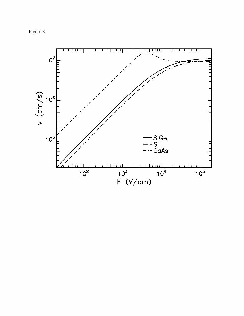
Figure 3

Figure 4
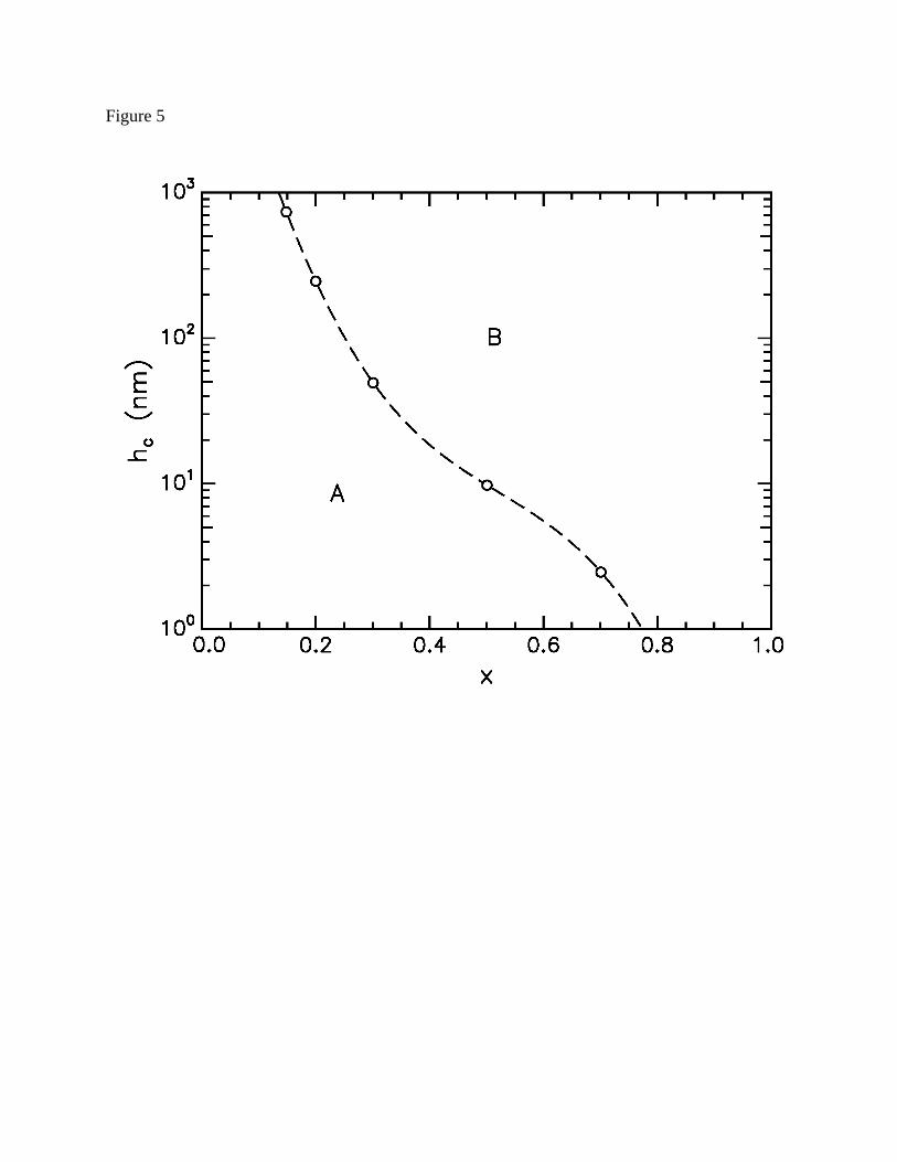
Figure 5
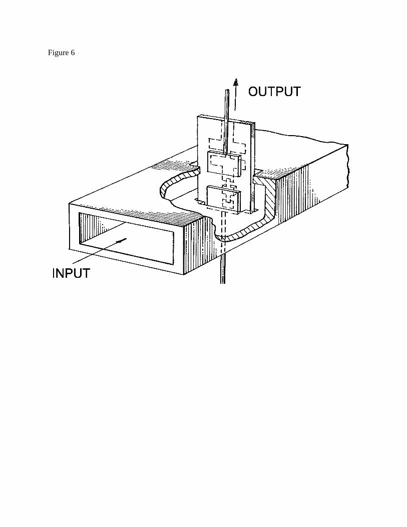
Figure 6
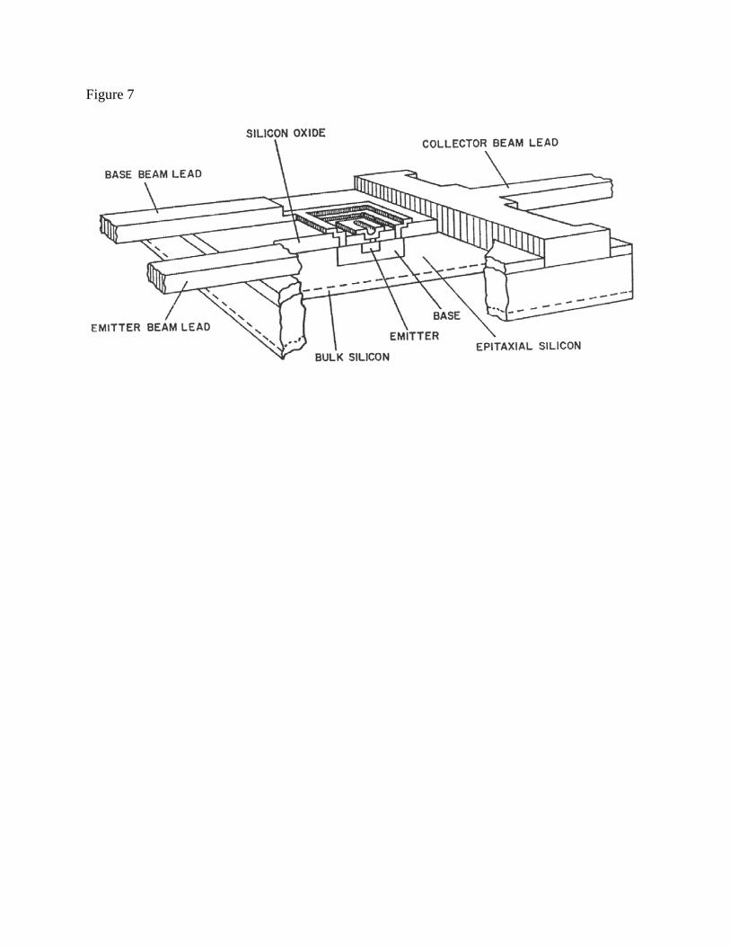
Figure 7
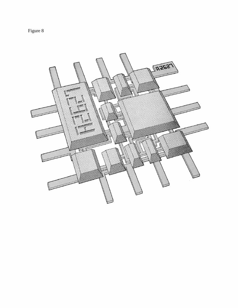
Figure 8
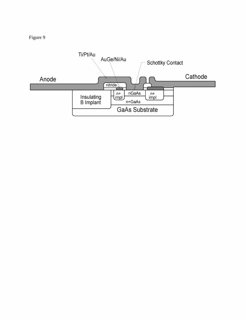
Figure 9
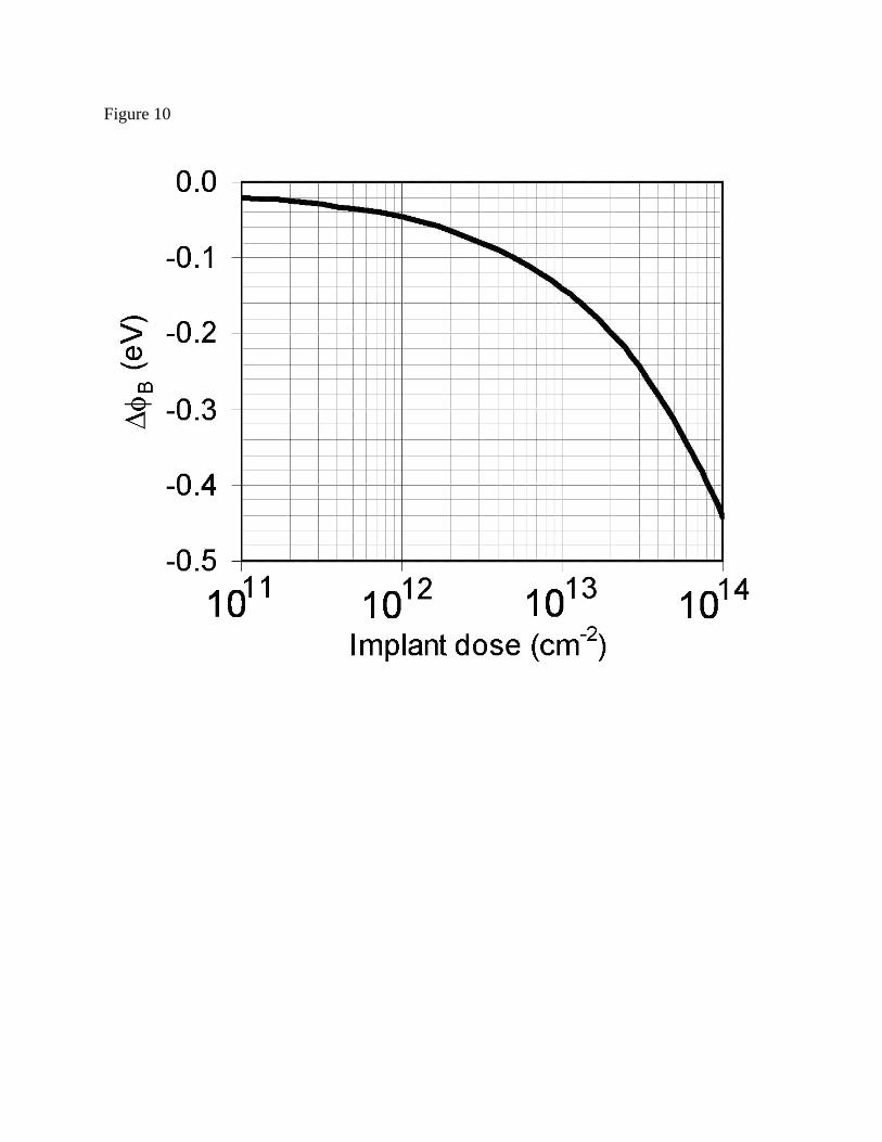
Figure 10
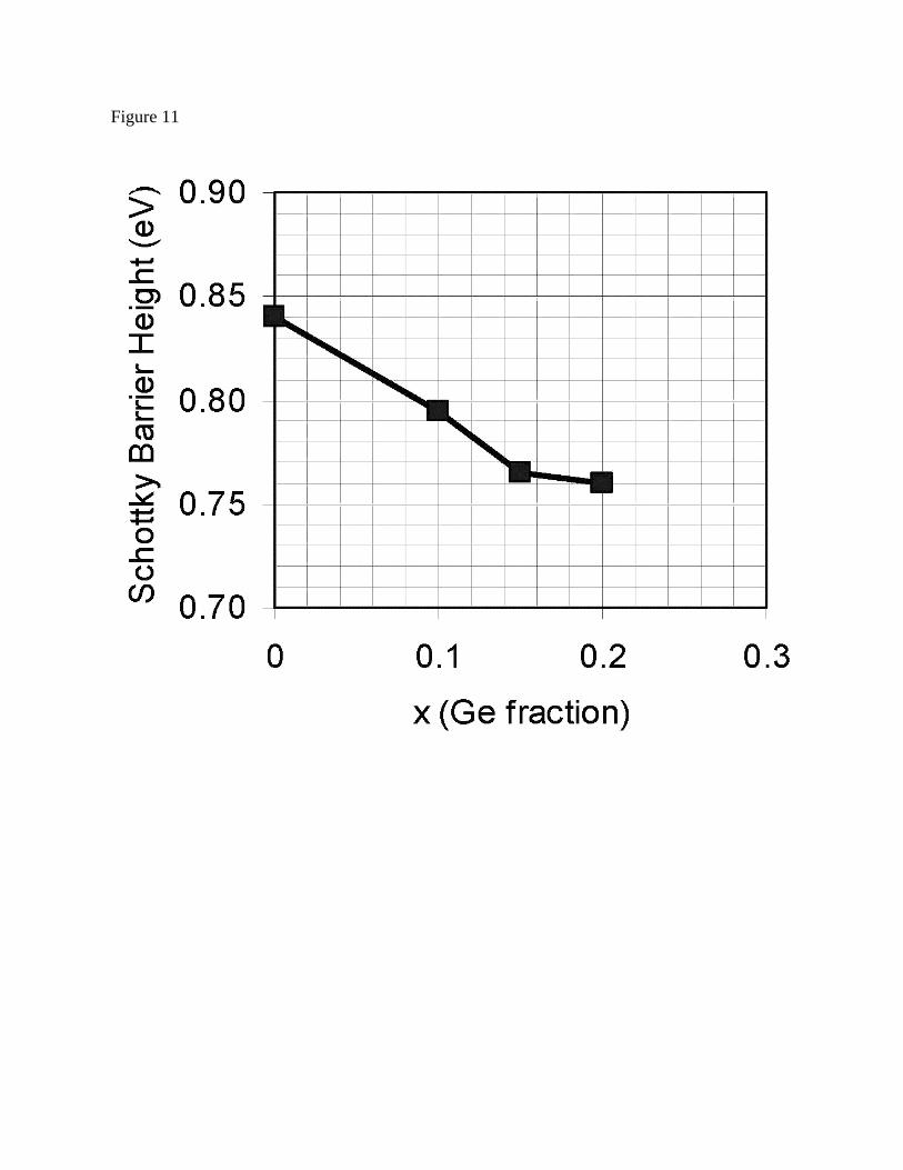
Figure 11

Figure 12

Figure 13

Figure 14 (a)

Figure 14 (b)

Figure 14 (c)
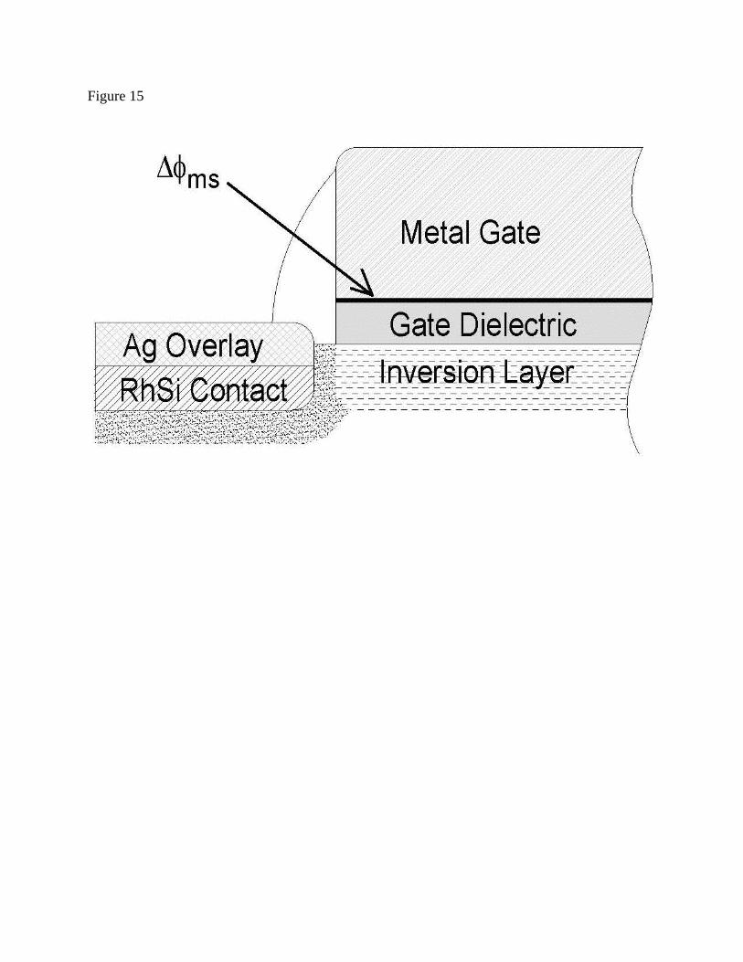
Figure 15

Figure 16
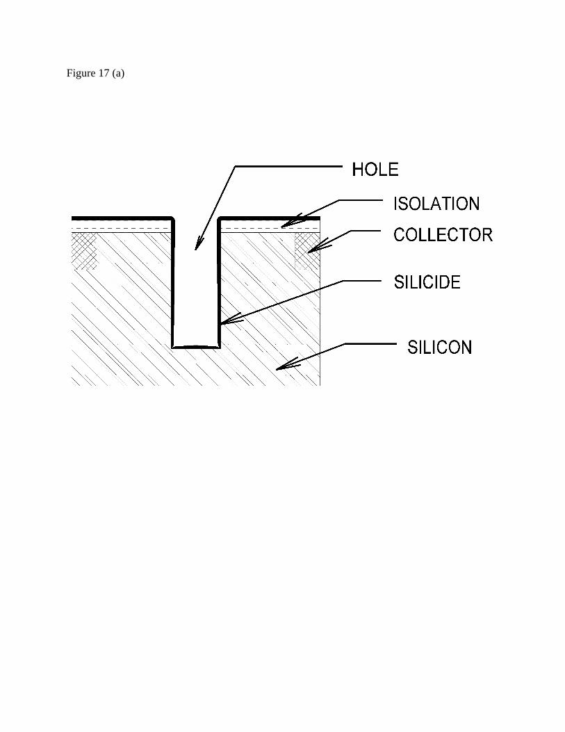
Figure 17 (a)
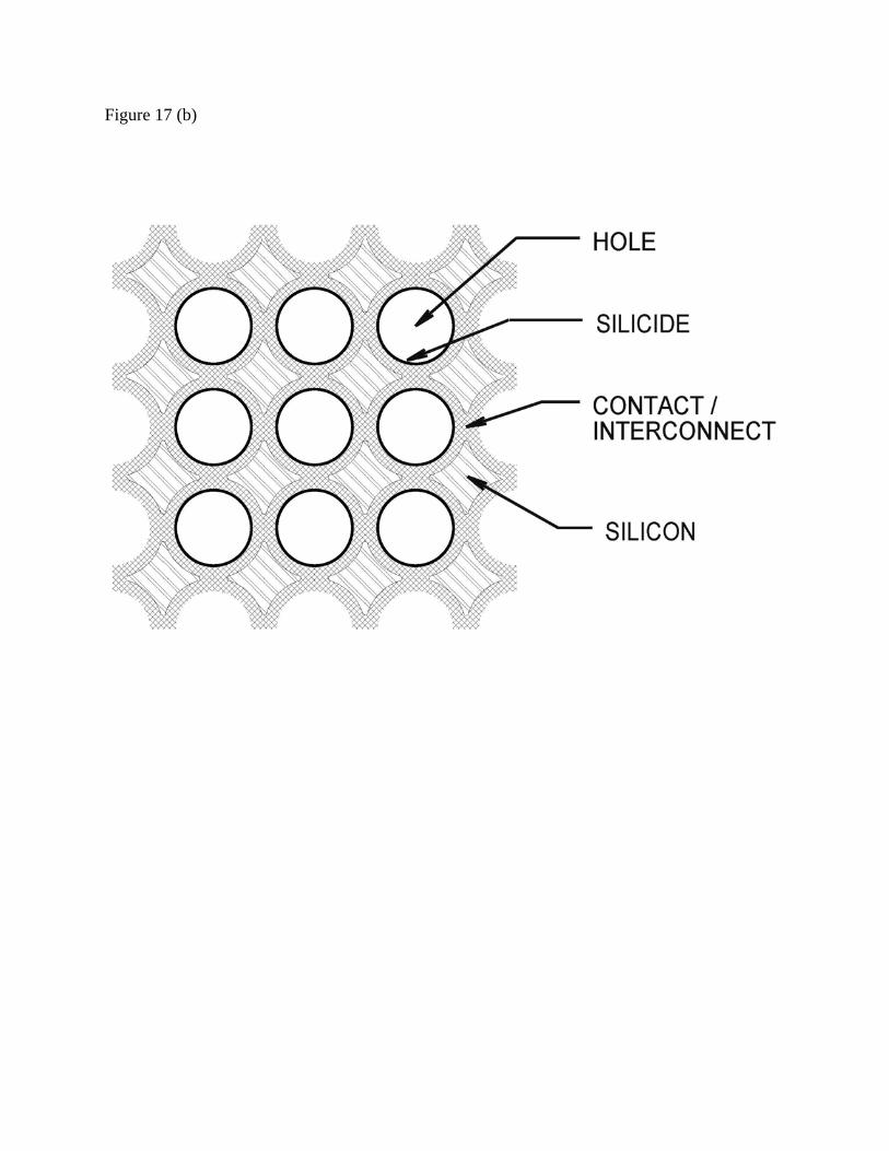
Figure 17 (b)

Figure 18


![Synthesis of Rhodium, Iridium, and Palladium Tetranuclear Complexes Directed by 2,6-Dimercaptopyridine. X-ray Crystal Structure of [Rh 4 (μ-PyS 2 ) 2 (cod) 4 ] (cod = 1,5-Cyclooctadiene)](https://static.fdokumen.com/doc/165x107/6337b5bace400ca69809223f/synthesis-of-rhodium-iridium-and-palladium-tetranuclear-complexes-directed-by.jpg)


![“(Acetylacetonato)carbonyl{dicyclohexyl[4-(N,N-dimethylamino)phenyl] phosphine}rhodium(I)](https://static.fdokumen.com/doc/165x107/631b64dc7abff1d7c20ae8e4/acetylacetonatocarbonyldicyclohexyl4-nn-dimethylaminophenyl-phosphinerhodiumi.jpg)