Physical and chemical changes of polystyrene nanospheres irradiated with laser
6
Physical and Chemical Changes of Polystyrene Nanospheres Irradiated with Laser Mohd Ubaidillah Mustafa, Mohd Arif Agam, Nor Rashidah Md. Juremi, Farizan Mohamad, Pratama Jujur Wibawa et al. Citation: AIP Conf. Proc. 1341, 67 (2011); doi: 10.1063/1.3586956 View online: http://dx.doi.org/10.1063/1.3586956 View Table of Contents: http://proceedings.aip.org/dbt/dbt.jsp?KEY=APCPCS&Volume=1341&Issue=1 Published by the American Institute of Physics. Related Articles The origin of 0.78eV line of the dislocation related luminescence in silicon J. Appl. Phys. 112, 063528 (2012) Radiation tolerance of ultra-thin Formvar films Appl. Phys. Lett. 101, 071908 (2012) Dynamics of the defect-mediated desorption of alkali halide surfaces Low Temp. Phys. 38, 774 (2012) In-situ transmission electron microscopy of partial-dislocation glide in 4H-SiC under electron radiation Appl. Phys. Lett. 101, 042102 (2012) Space charge modeling in electron-beam irradiated polyethylene: Fitting model and experiments J. Appl. Phys. 112, 023704 (2012) Additional information on AIP Conf. Proc. Journal Homepage: http://proceedings.aip.org/ Journal Information: http://proceedings.aip.org/about/about_the_proceedings Top downloads: http://proceedings.aip.org/dbt/most_downloaded.jsp?KEY=APCPCS Information for Authors: http://proceedings.aip.org/authors/information_for_authors Downloaded 10 Oct 2012 to 203.82.80.77. Redistribution subject to AIP license or copyright; see http://proceedings.aip.org/about/rights_permissions
Transcript of Physical and chemical changes of polystyrene nanospheres irradiated with laser

Physical and Chemical Changes of Polystyrene Nanospheres Irradiatedwith LaserMohd Ubaidillah Mustafa, Mohd Arif Agam, Nor Rashidah Md. Juremi, Farizan Mohamad, Pratama Jujur Wibawa et al. Citation: AIP Conf. Proc. 1341, 67 (2011); doi: 10.1063/1.3586956 View online: http://dx.doi.org/10.1063/1.3586956 View Table of Contents: http://proceedings.aip.org/dbt/dbt.jsp?KEY=APCPCS&Volume=1341&Issue=1 Published by the American Institute of Physics. Related ArticlesThe origin of 0.78eV line of the dislocation related luminescence in silicon J. Appl. Phys. 112, 063528 (2012) Radiation tolerance of ultra-thin Formvar films Appl. Phys. Lett. 101, 071908 (2012) Dynamics of the defect-mediated desorption of alkali halide surfaces Low Temp. Phys. 38, 774 (2012) In-situ transmission electron microscopy of partial-dislocation glide in 4H-SiC under electron radiation Appl. Phys. Lett. 101, 042102 (2012) Space charge modeling in electron-beam irradiated polyethylene: Fitting model and experiments J. Appl. Phys. 112, 023704 (2012) Additional information on AIP Conf. Proc.Journal Homepage: http://proceedings.aip.org/ Journal Information: http://proceedings.aip.org/about/about_the_proceedings Top downloads: http://proceedings.aip.org/dbt/most_downloaded.jsp?KEY=APCPCS Information for Authors: http://proceedings.aip.org/authors/information_for_authors
Downloaded 10 Oct 2012 to 203.82.80.77. Redistribution subject to AIP license or copyright; see http://proceedings.aip.org/about/rights_permissions

Physical and Chemical Changes of Polystyrene Nanospheres Irradiated with Laser
Mohd Ubaidillah Mustafaa, Mohd Arif Agam*b , Nor Rashidah Md Juremia, Farizan Mohamada, Pratama Jujur Wibawaa, and Ahmad Hadi Alib
a Microelectronic and Nanotechnology - Shamsudin Research Centre, Faculty of Electrical and Electronic Engineering, University Tun Hussein Onn Malaysia
b Faculty of Science, Art and Heritage, University Tun Hussein Onn Malaysia. *Email: [email protected]
Abstract. It has been reported that polymer resist such as PMMA (Poly(methyl methacrylate) which is a well known and commonly used polymer resist for fabrication of electronic devices can show zwitter characteristic due to over exposure to electron beam radiation[1]. Overexposed PMMA tend to changes their molecular structure to either become negative or positive resist corresponded to electron beam irradiation doses. These characteristic was due to crosslinking and scissors of the PMMA molecular structures, but till now the understanding of crosslinking and scissors of the polymer resist molecular structure due to electron beam exposure were still unknown to researchers [2-5].Previously we have over exposed polystyrene nanospheres to various radiation sources, such as electron beam, solar radiation and laser, which is another compound that can act as polymer resist. We investigated the physical and chemical structures of the irradiated polystyrene nanospheres with FTIR analysis. It is found that the physical and chemical changes of the irradiated polystyrene were found to be corresponded with the radiation dosages. Later, combining Laser irradiation and Reactive Ion Etching manipulation, created a facile technique that we called as LARIEA NSL (Laser and Reactive Ion Etching Assisted Nanosphere Lithography) which can be a facile technique to fabricate controllable carbonaceous nanoparticles for applications such as lithographic mask, catalysts and heavy metal absorbers.
Keywords: polymer resist, zwitter characteristic, polystyrene nanospheres, LARIEA NSL PACS: 61.48.Gh; 61.46.Bc; 62.23.St; 68.37.Hk; 81.16.Dn
INTRODUCTION
Nanosphere lithography(NSL) is versatile hybrid bottom-up technique in fabrication nanostructure materials, that is facile, general in substrates or materials used, cheap and can be mass produce (parallel technique), is through a technique [5-10]. The technique was widely used and was endorsed by Richard Van Duyne group where NSL was found to be a very adaptable technique in producing nanomaterials, which have many potential applications such as catalysts, photonic materials and semiconductor devices [11-19].
Incorporating NSL with other complimentary techniques such as electron beam, heat treatment, chemical manipulation, and reactive ion etching [20] has shown the abilities to increase the versatility of NSL in producing either as mask patterning or fabrication nanoparticles on substrates surface. Thus combining NSL with other complimentary techniques can be categorized as the secondary lithography stage
of NSL technique. The focused characteristic of these secondary lithographic stages for NSL is to be able to modify the nanopheres structure after they were let self-assembled on substrate surfaces.
One of the attempt at these secondary lithography stage of NSL is the over exposure of electron beam irradiation to polystyrene nanospheres, where, the electron beam is acting as manipulating agent. Experimental results have shown that, both the sizes and shapes of the nanospheres can be modified in a controlled manner depended on electron beam doses [20-21]. Modifying polystyrene nanospheres structure by electron beam irradiation has created a new lithography mask that otherwise is not available through self-assemble of the nanospheres alone. The mask created from irradiated and non-irradiated nanospheres can be used to precisely pattern periodic nanoparticle arrays.
Enabling Science and NanotechnologyAIP Conf. Proc. 1341, 67-71 (2011); doi: 10.1063/1.3586956
© 2011 American Institute of Physics 978-0-7354-0897-5/$30.00
67
Downloaded 10 Oct 2012 to 203.82.80.77. Redistribution subject to AIP license or copyright; see http://proceedings.aip.org/about/rights_permissions
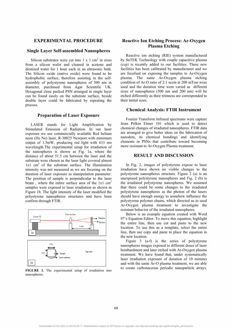
EXPERIMENTAL PROCEDURE
Single Layer Self-assembled Nanospheres Silicon substrates were cut into 1 x 1 cm2 in sizes
from a silicon wafer and cleaned in acetone and dionized water for 1 hour each in an ultrasonic bath. The Silicon oxide (native oxide) were found to be hydrophobic surface, therefore assisting in the self-assembly of polystyrene nanospheres of 500 nm in diameter, purchased from Agar Scientific UK. Hexagonal close packed PSN arranged in single layer can be found easily on the substrate surface, beside double layer could be fabricated by repeating the process.
Preparation of Laser Exposure
LASER stands for Light Amplification by
Stimulated Emission of Radiation. In our laser exposure we use commercially available Red helium neon (He Ne) laser, R-30025 Newport with minimum output of 1.5mW, producing red light with 633 nm wavelength.The experimental setup for irradiation of the nanospheres is shown as Fig. 1a, where the distance of about 51.5 cm between the laser and the substrate were chosen as the laser light covered almost 1x1 cm2 of the substrate surface. The illumination intensity was not measured as we are focusing on the duration of laser exposure as manipulation parameter. The position of sample is perpendicular to the laser beam , where the entire surface area of the 1x1 cm2 samples were exposed to laser irradiation as shown in Figure 1b. The light intensity of the laser modified the polystyrene nanospheres structures and have been confirm through FTIR.
FIGURE 1. The experimental setup of irradiation into nanospheres.
Reactive Ion Etching Process: Ar-Oxygen Plasma Etching
Reactive ion etching (RIE) system manufactured
by SnTEK Technology with couple capacitive plasma (ccp) is recently added to our facilities. These new facilities has been calibrated by manufacturer and we are focufsed on exposing the samples to Ar-Oxygen plasma. The same Ar-Oxygen plasma etching condition of Ar:O ratio of 2:1 sccm at 200 mTorr were used and the duration time were varied as different sizes of nanospheres (500 nm and 200 nm) will be etched differently as their trimness are corresponded to their initial sizes.
Chemical Analysis: FTIR Instrument Fourier Transform Infrared spectrums were capture
from Pelkin Elmer 101 which is used to detect chemical changes of irradiated nanospheres. FTIR data are arranged to give better ideas on the fabrication of nanodots, its chemical bondings and identifying elements in PSNs that contribute toward becoming more resistant to Ar-Oxygen Plasma treatment.
RESULT AND DISCUSSION
In Fig. 2, images of polystyrene expose to laser
irradiation have shown no visible changes to the polystyrene nanospheres structure. Figure 2 (a) is an unexposed polystyrene nanospheres and Fig. 2 (b) is the irradiated polystyrene nanospheres. We assumed that there could be some changes to the irradiated polystyrene nanospheres as the photon of the lasers should have enough energy to somehow influence the polystyrene polymer chains, which directed us to used Ar-Oxygen plasma treatment to investigate the resistant behavior of the irradiated nanospheres.
Below is an example equation created with Word 97’s Equation Editor. To move this equation, highlight the entire line, then use cut and paste to the new location. To use this as a template, select the entire line, then use copy and paste to place the equation in the new location.
Figure 3 (a-f) is the series of polystyrene nanospheres images exposed to different doses of laser bombardment and later etched with Ar-Oxygen plasma treatment. We have found that, under systematically laser irradiation exposure of duration of 10 minutes and with the same Ar-O plasma treatment, we are able to create carbonaceous periodic nanoparticle arrays.
68
Downloaded 10 Oct 2012 to 203.82.80.77. Redistribution subject to AIP license or copyright; see http://proceedings.aip.org/about/rights_permissions

FIGURE 2. Before (2a) and after (2b) He Ne laser bombardment into polystyrene nanospheres.
FIGURE 3. (a-f) is the sequence of polystyrene nanospheres images exposed to different doses of laser bombardment and later etched with Ar-Oxygen(ratio 2:1) plasma treatment. Average of PSNs diameter 5(a-f) (300nm;300nm;334nm;334nm; 334nm;334nm from their initial size of 500nm).
The Ar-O plasma treatment (ratio 2:1 sccm for 20s:
for 500 nm diameter of PSNs) was used as a tool to prove that the chemical structure of the polystyrene polymer chains has been influence by laser irradiation. We assumed that if the polystyrene polymer chains are affected by the laser irradiation, there should be some characteristic differences of the irradiated polystyrene polymer if expose to reactive ion etching processes compared to the etching rate for ordinary PSNs.
The laser irradiation has somehow changes the nanospheres structure to become more resistant toward Ar-Oxygen plasma etching treatment. The original size of the PSNs are 500 nm in diameter and overexposure
of laser irradiation and subsequence of Ar-Oxygen plasma treatment, the nanomaterials of 300-350 nm in sizes can be fabricated. The PSNs seem to react differently in various etching condition where the gases used are critical factors determining the etching rate of bare PSNs.
In Figure 2 a), the original nanospheres if etch by Ar-Oxygen plasma treatments were found to be etch to 300 nm diameters or shrunk to about 40% from its original size of 500 nm in diameter. Irradiated polystyrene images to different duration of laser irradiation and later etched with Ar-Oxygen plasma treatment.
2a 2b
3a
0 min
3b
10 min
3c
20 min
3d
30 min
3e
40 min
3f
50 min
69
Downloaded 10 Oct 2012 to 203.82.80.77. Redistribution subject to AIP license or copyright; see http://proceedings.aip.org/about/rights_permissions
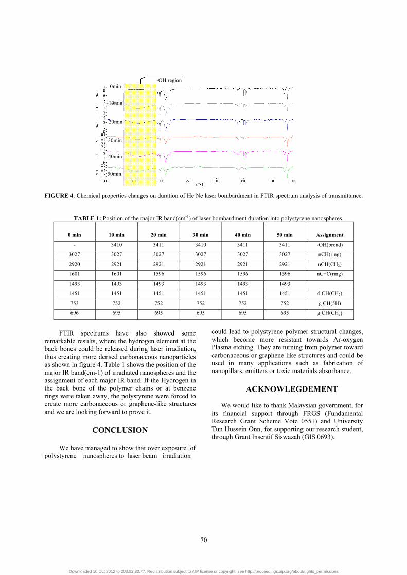
FIGURE 4. Chemical properties changes on duration of He Ne laser bombardment in FTIR spectrum analysis of transmittance.
TABLE 1: Position of the major IR band(cm-1) of laser bombardment duration into polystyrene nanospheres.
0 min
10 min
20 min
30 min
40 min
50 min
Assignment
- 3410 3411 3410 3411 3411 -OH(broad)
3027 3027 3027 3027 3027 3027 nCH(ring)
2920 2921 2921 2921 2921 2921 nCH(CH2)
1601 1601 1596 1596 1596 1596 nC=C(ring)
1493 1493 1493 1493 1493 1493
1451 1451 1451 1451 1451 1451 d CH(CH2)
753 752 752 752 752 752 g CH(5H)
696 695 695 695 695 695 g CH(CH2)
FTIR spectrums have also showed some
remarkable results, where the hydrogen element at the back bones could be released during laser irradiation, thus creating more densed carbonaceous nanoparticles as shown in figure 4. Table 1 shows the position of the major IR band(cm-1) of irradiated nanospheres and the assignment of each major IR band. If the Hydrogen in the back bone of the polymer chains or at benzene rings were taken away, the polystyrene were forced to create more carbonaceous or graphene-like structures and we are looking forward to prove it.
CONCLUSION
We have managed to show that over exposure of
polystyrene nanospheres to laser beam irradiation
could lead to polystyrene polymer structural changes, which become more resistant towards Ar-oxygen Plasma etching. They are turning from polymer toward carbonaceous or graphene like structures and could be used in many applications such as fabrication of nanopillars, emitters or toxic materials absorbance.
ACKNOWLEGDEMENT
We would like to thank Malaysian government, for
its financial support through FRGS (Fundamental Research Grant Scheme Vote 0551) and University Tun Hussein Onn, for supporting our research student, through Grant Insentif Siswazah (GIS 0693).
0min
10min
20min
30min
40min
50min
-OH region
70
Downloaded 10 Oct 2012 to 203.82.80.77. Redistribution subject to AIP license or copyright; see http://proceedings.aip.org/about/rights_permissions
REFERENCES
1. Bhuvana, T., Kulkarni, G U, “ Polystyrene as a zwitter resist in electron lithography based electroless patterning of gold”, Bull. Mater. Sci., 2008, Vol. 31, pp 201-206,
2. Agam, M.A., Guo, Q., “Electron beam modification of polymer nanospheres”, J. Nanosci. Nanotechno. 2007, Vol. 10, pp3615-3619,
3. Chen, J.K., Ko, F.H., Chang, F.C., “Structural transformation of acrylic resin upon controlled electron-beam exposure yield and negative resists”, Nanotechnology ,2005, vol. 17 pp.4399,
4. Hoole, A.C.F., Welland M.E., Broers, A. N., “Negative PMMA as a high-resolution resist-the limit and possibilities”, Semicond. Sci. Technol. Vol. 12, pp.1166-1170, 1997
5. Zailer, I., Frost, J.E.F., Chabasseur-Molyneux, V., Ford, C.J.B., Pepper, M., “Crosslinked PMMA as a high resolution negative resist for electron beam lithography and applications for physics of low-dimensional structures”, Semicond. Sci. Technol. 1996, Vol. 11, pp.1235-1238,
6. Kim, B.J., Hyunjung Jung, Kim, H.Y., Joona Bang, Jihyun Kim, “Fabrication of Nanorods by ICP etching via SiO2 NSL”, Thin Solid Films, 2009, Vol. 517, pp.3859-3861.
7. Christian Patzig, Bodo Fuhrmann, Leipner, H.S., Bernd Rauschenbach, “Si Nanoculomns on NSL template Substrates: Effects of sphere size and substrate temperature”, Journal of Nanoscience and Nanotechnology, 2008, Vol. 8, pp 1-7
8. Zhou, C.M., Gall, D., “Suface patterning by NSL for layer growth with ordered pores”, Thin Solid Films, 2007, Vol. 516, pp. 433-437
9. Canpean, V., Astilean, S., Petrisor Jr, T., Ciascai, I., “Convective assembly of 2D NSL masks”, Materials Letter , 2009,Vol. 63,pp.1834-1836
10. Cong, C.X., Yu, T., Ni, Z.H., Liu, L., Shen Z.X., Huang, W., “Fabrication of Graphene Nanodisk Arrays Using NSL”, J Phys Chem C, 2009, Vol. 113, pp.6529-6532
11. Jiha Sung, Kosuda K.M., Jing Zao, Elam, J.W., Spears, K.G., Van Duyne R. P., “Stability of silver nanoparticles fabricated by NSL and atomic layer deposition to Femtosecond Laser Excitation”, J. Phys. Chem. C, 2008, Vol. 112, pp. 5707-5714.
12. Hulteen, J.C., and Van Duyne, R.P., “Nanosphere Lithography: A Material General Fabrication Process For Periodic Particle Array Surfaces”, J. Vac. Sci. Technol. A, 1995, vol. 13, pp1553-1558
13. Haes, A.J., Haynes, C.L., Van Duyne, R.P. “Nanosphere Lithography: Self-Assembled Photonic and Magnetic Materials”, Materials Research Society Fall Meeting, Boston, MA, November 28, 2000.
14. Jensen, T.R., Schatz, G.C., And Van Duyne R.P., “Nanosphere Lithography: Surface Plasmon Resonance Spectrum Of A Periodic Array Of Silver Nanoparticles By Ultraviolet- Visible Extinction Spectroscopy And Electrodynamic Modelling”, J. Phys. Chem. B, 1999, 103, pp 2394–2401.
15. Hulteen, J.C., Treichel, D.A., Smith, M.T., Duval, M.L., Jensen, T.R., And Van Duyne, R.P., “Nanosphere Lithography: Size-Tunable Silver Nanoparticle And Surface Cluster Arrays”, J. Phys. Chem. B, 1999, 103, pp 3854–3863.
16. Malinsky, M.D., Kelly K.L., Schatz G.C., And Van Duyne, R.P., “Nanosphere Lithography: Effect Of Substrate On The Localized Surface Plasmon Resonance Spectrum Of Silver Nanoparticles”, J. Phys. Chem. B, 2001, 105, pp 2343–2350
17. Haes, A.J., Jing Zhao, Shengli Zou, Own, C.S., Marks, L.D., Schatz G.C., & Van Duyne, R.P., “ Solution-Phase, Triangular Ag Nanotriangles Fabricated by Nanosphere Lithography”, J. Phys. Chem. B 2005, 109, pp.11158-11162
18. Haynes, C.L., Mcfarland, A.D., Smith, M.T., Hulteen, J.C., and Van Duyne, R.P., “Angle-resolved nanosphere lithography: manipulation of nanoparticle size, shape, and interparticle spacing”, J. Phys. Chem. B, 2002, 106, pp.1898-1902.
19. Ormonde, A.D., Hicks, E.C.M., Jimmy Castillo, Van Duyne R.P., “Nanosphere lithography: fabrication of large area Ag nanoparticle arrays by convective self-assembly and their by scanning UV-visible extinction spectroscopy”, Langmuir, 2004, 20, 6927-6931
20. Xiaoyu Zhang, Hicks E.M., Jiang Zhao, Schatz G.C., and Van Duyne R.P., “Electrochemical tuning of silver nanoparticles fabricated by nanosphere lithography”, Nano lett. 2005, vol. 5, no. 7, pp 1503 – 1507.
21. Agam, M.A., “An investigation of physical processes in nanosphere lithography”, PhD Thesis, Nanoscale Physics Research Laboratory, School of Physics and Astronomy, Birmingham University, U.K 2006.
71
Downloaded 10 Oct 2012 to 203.82.80.77. Redistribution subject to AIP license or copyright; see http://proceedings.aip.org/about/rights_permissions