Bioengineered Skin Intended for Skin Disease Modeling - MDPI
Upload
khangminh22Category
view
0download
0
ii
“BVH˙book” — 2013/10/24 — 10:07 — page a — #1 ii
ii
ii

ii
“BVH˙book” — 2013/10/24 — 10:07 — page b — #2 ii
ii
ii

ii
“BVH˙book” — 2013/10/24 — 10:07 — page c — #3 ii
ii
ii
Fotonische huid gebaseerd op integratie van optische sensorenen uitleeseenheden in polymere substraten
Photonic Skin Based on Polymer Embedding of Optical Sensorsand Interrogation Units
Bram Van Hoe
Promotoren: prof. dr. ir. G. Van Steenberge, prof. dr. ir. P. Van DaeleProefschrift ingediend tot het behalen van de graad van Doctor in de Ingenieurswetenschappen: Elektrotechniek
Vakgroep Elektronica en InformatiesystemenVoorzitter: prof. dr. ir. J. Van CampenhoutFaculteit Ingenieurswetenschappen en ArchitectuurAcademiejaar 2013 - 2014

ii
“BVH˙book” — 2013/10/24 — 10:07 — page d — #4 ii
ii
ii
ISBN 978-90-8578-636-8NUR 959Wettelijk depot: D/2013/10.500/69

ii
“BVH˙book” — 2013/10/24 — 10:07 — page e — #5 ii
ii
ii
Universiteit GentFaculteit Ingenieurswetenschappen en Architectuur
Vakgroep Elektronica en Informatiesystemen
Promotoren: prof. dr. ir. G. Van Steenbergeprof. dr. ir. P. Van Daele
Centre for Microsystems Technology (CMST)Vakgroep Elektronica en InformatiesystemenTechnologiepark 914AB-9052 Zwijnaarde
Tel.: +32-9-264.53.70Fax.: +32-9-264.53.74
Examencomissie: prof. dr. ir. L. Taerwe – Voorzitterdr. ir. E. Bosman – Secretarisprof. dr. ir. F. Berghmansprof. dr. P. Dubruelprof. dr. D.J. Webbprof. dr. ir. D. Van Thourhoutdr. J. Vlekken
Onderzoek gefinancierd met een specialisatiebeurs vanhet Instituut voor de Aanmoediging van Innovatie doorWetenschap en Technologie in Vlaanderen(IWT-Vlaanderen).
Proefschrift ingediend tot het behalen van de graad vanDoctor in de Ingenieurswetenschappen: Elektrotechniek
Academiejaar 2013-2014

ii
“BVH˙book” — 2013/10/24 — 10:07 — page f — #6 ii
ii
ii

ii
“BVH˙book” — 2013/10/24 — 10:07 — page i — #7 ii
ii
ii
Dankwoord
Het boek dat u nu vasthebt is er enkel kunnen komen door een heleboel mensendie allemaal een bijdrage hebben geleverd hiervoor op heel wat verschillendegebieden.Ik begin bij CMST, het Centrum voor Microsysteem Technologie, waar ik na mijnmasterproef als doctoraatsstudent ben begonnen. Vooreerst wil ik mijn promoto-ren, Geert Van Steenberge en Peter Van Daele, bedanken. Ze gaven me de kansom aan dit doctoraat te beginnen en zorgden voor veel inspiratie tijdens mijn on-derzoek. Daarnaast boden ze mij de mogelijkheid om intensief betrokken te zijnbij nationale en internationale projecten, en om onderzoeksresultaten te publice-ren en te presenteren op internationale conferenties.Verder wil ik ook Andre Van Calster en het CMST management bedanken. Zijhebben CMST gemaakt tot wat het nu is: een onderzoeksgroep, deel uitmakendvan zowel Universiteit Gent als het onderzoekscentrum Imec, en bestaande uitbijna zestig mensen met een state-of-the-art cleanroom infrastructuur en een in-drukwekkende portfolio van onderzoeksprojecten.De leden van de jury hebben veel interessante opmerkingen en commentarenaangebracht. Ik wil hen bedanken voor de tijd die ze in mijn proefschrift heb-ben geınvesteerd. Erwin, Jeroen, Geert en Ann wil ik graag bedanken voor hetreviewen van een of meerdere hoofstukken.Het optische (of correcter “Polymer Photonics and Laser Technology”) team vanCMST hoort zeker ook in dit rijtje thuis. Geert, Erwin, Jeroen, Sandeep, San-jeev, Kamal, Pankaj, Nuria en Ahmed wil ik bedanken voor de vele interessantediscussies, nieuwe ideeen en verhelderende uitleg, in combinatie met de nodigeambiance.Een groot deel van dit doctoraat is gebaseerd op technologische processen dieworden verricht in een cleanroom omgeving met hoogtechnologische toestellen.Ik wil dan ook de mensen bedanken die voor mij of met mij verschillende pro-cesstappen hebben uitgevoerd. Steven voor het laserwerk (inclusief opstart vanons nieuw 3DMM systeem) en de liefde voor blauw-wit, Peter G. voor het uit-voeren van chip verdunning, waveguide processing, litho- en etsstappen, en veleandere probeersels. Dieter en Filip V. voor het sputteren en RIE’en, Bjorn voorde dispenser- en Tresky-testjes, Filip T. voor de molds en andere technische hulp-middelen, David voor het SEM werk, en het hele CR support en EIP team voorde ondersteuning en het safety management. Dr. Tresky en Dr. Bosman wil ik

ii
“BVH˙book” — 2013/10/24 — 10:07 — page ii — #8 ii
ii
ii
ii Dankwoord
bedanken voor de hulp en het technisch vernuft bij het plaatsen van dunne chips.Ook de collega’s van de smart power group (“de designers”) wil ik graag be-danken voor alle hulp bij elektronicahindernissen. Jindrich in het bijzonder, voorde technische bijstand bij zeer uiteenlopende problemen, gaande van gecrashtelaptops tot verbrande Ford Mondeo-ruitensproeiverwarmelementjes...Collega’s en ex-collega’s van “onzen bureau”, bedankt voor alle mooie herinne-ringen! Verder ook Katrien om altijd klaar te staan om administratieve vragente beantwoorden en Peter S. voor de IT ondersteuning. Ik wil bij uitbreidingook alle andere collega’s van CMST bedanken voor alle hulp en de uitstekende(werk)sfeer!Niet alleen met de collega’s binnen CMST, maar ook met andere onderzoeks-groepen had ik een zeer goed contact binnen de IWT-SBO projecten FAOS enSSC, en de EU-FP7 projecten Phosfos en Actmost. Die combinatie van uiteen-lopende expertise heeft niet alleen geleid tot gemeenschappelijke publicaties ennieuwe inzichten, maar ook tot een netwerk van mensen die ik graag tegenkomop projectmeetings, conferenties of workshops.In het bijzonder wil ik de collega’s van de (Ugent) Polymer Chemistry & Bio-materials Group (“den S4”) vermelden voor de materiaalontwikkelingen en -karakterisatie. De PMA groep in Leuven (KUL) wil ik graag bedanken voorhet werk rond de mechanische karakterisatie van de VCSEL druksensor. Ookde (Ugent) Mechanica van Materialen en Structuren onderzoeksgroep mag hierniet ontbreken, in het bijzonder Geert Luyckx, voor het gebruik van testopstel-lingen (o.a. elektrodynamische shaker) en demonstratoren. Verder was het Brus-sels Photonics Team (VUB) een onmisbare schakel in dit doctoraatsonderzoek.Vooreerst vermeld ik de Fiber Group, in het bijzonder Sanne Sulejmani, CamilleSonnenfeld, Thomas Geernaert en Francis Berghmans, voor het werk rond micro-gestructureerde vezelsensoren. Verder Jurgen Van Erps voor de simulaties enexpertise rond optische koppelstructuren. Ook Heidi Ottevaere en de andereB-Phot collega’s voor gebruik van en uitleg bij allerlei meetapparatuur. Jan VanRoosbroeck en Jo Vlekken van FBGS International wil ik graag bedanken voorde samenwerking rond ingebedde DTGs. I would also like to acknowledge thepeople from the Aston Institute of Photonic Technologies in Birmingham for theexcellent collaboration within Phosfos. Thank you, David Webb, Kate Sugdenand Graham Lee, for all your efforts on polymer optical fiber sensors and FBG in-terrogation systems. A special thanks to Graham, I admire your drive to achieveresults and very much enjoyed working together.Greetje Godier, Tom De Geyter en Johan Paul van Flamac voor het gebruik vande nano-intender en de ondersteuning bij experimenten. Deben Lamon en Giu-seppe Melpignano voor het thesis- en stagewerk rond de VCSEL druksensor.
Bedankt studiegenoten, in het bijzonder Yannick, Deben en Kristof. Misschienherkennen jullie hier en daar wel enkele ideeen van ons hardware-ontwerpprojectuit 2007.

ii
“BVH˙book” — 2013/10/24 — 10:07 — page iii — #9 ii
ii
ii
iii
Veel collega’s zijn ondertussen goede vrienden geworden...Ik wil Pritesh, Frederick & Adinda, Thomas & Eveline, Ann & Alwin en Fabricebedanken voor de onvergetelijke trip naar India. Jindrich, Ann & Alwin voor defijne roadtrip in de US. Tom voor het bijhouden van mijn oneliners (“het leven zitvol anticipaties!!”), Rik voor de Extra Time babbels in de gang. Erwin voor de lan-cering van onze DJ carriere, alsook de organisatie van vele culturele activiteiten(Hans Teeuwen-avond, boefparty, wok dynasty uitstapjes, ...).Ook het CMST voetbalteam mag hier niet ontbreken. Het was een hele eer samenmet jullie de kleuren van CMST te verdedigen. De voorzittersverkiezing metbijhorend ribbekesfestijn is elk jaar iets om naar uit te kijken. Ik heb met veelgenoegen het voorzittersambt gedurende een seizoen mogen opnemen. Verderhebben ook de CMST barbecues een aantal onuitwisbare indrukken nagelaten,bedankt aan iedereen die dit evenement elk jaar tot zo’n succes maakt.Sport en ontspanning zijn cruciaal tijdens het leven, en zeker tijdens een docto-raat. Daarom wil ook buiten CMST een aantal mensen bedanken.Om te beginnen de kerncompetitieploeg Brildesign Deinze: ik ben er zeker vandat ons nog vele mooie seizoenen te wachten staan. Squashpartner Wim mag hierniet ontbreken, na een sabbatjaar vliegen we er volgend jaar opnieuw in! Ook deGent Symphonic Band hoort in dit rijtje thuis. Samen musiceren en concerterenblijft iets speciaal, zelfs na bijna 20 jaar! Verder wil ik de wijnclub-bende aka dewijnzero’s: Wim, Dhondt, Baeck, Ben en Cedric bedanken. Onze maandelijksebijeenkomsten zijn altijd iets om naar uit te kijken, of er nu wijn aan te pas komtof niet...Het is onmogelijk in dit korte dankwoord iedereen te vermelden. Een dikke merciaan alle andere vrienden voor de vele mooie momenten!
Ik wil ook graag mijn familie bedanken, in het bijzonder mijn zussen en pete-kind, Anke, Liesbet en Floris. Als ik jullie een cijfer moet geven, dan geef ik jullieeen 11!
Mijn ouders. Er zijn niet veel momenten waarop ik jullie expliciet bedank, maarik wil dit nu graag doen voor de perfecte zorgen gedurende al die jaren en voorde kansen die jullie me hebben gegeven.
En natuurlijk Elien. Storm, niemand anders weet zo goed wat ik voel of denk.Bedankt voor alle support die je me geeft! Van Ryhove wacht op ons!
Gent, oktober 2013Bram Van Hoe

ii
“BVH˙book” — 2013/10/24 — 10:07 — page iv — #10 ii
ii
ii

ii
“BVH˙book” — 2013/10/24 — 10:07 — page v — #11 ii
ii
ii
Table of Contents
Dankwoord i
Table of Contents v
List of Tables xi
List of Figures xiii
List of Acronyms xxiii
Samenvatting xxv
Summary xxxi
1 General introduction 11.1 Sensors . . . . . . . . . . . . . . . . . . . . . . . . . . . . . . . . . . . 11.2 Miniaturization . . . . . . . . . . . . . . . . . . . . . . . . . . . . . . 21.3 Optical systems . . . . . . . . . . . . . . . . . . . . . . . . . . . . . . 3
1.3.1 Optical datacommunication . . . . . . . . . . . . . . . . . . . 31.3.2 Optical sensing . . . . . . . . . . . . . . . . . . . . . . . . . . 41.3.3 Combination of optical datacommunication and sensing . . 7
1.4 Polymer embedding . . . . . . . . . . . . . . . . . . . . . . . . . . . 81.5 Photonic skins . . . . . . . . . . . . . . . . . . . . . . . . . . . . . . . 91.6 Problem statement and objectives . . . . . . . . . . . . . . . . . . . . 111.7 Research trajectory and dissertation structure . . . . . . . . . . . . . 131.8 Research context and related projects . . . . . . . . . . . . . . . . . . 141.9 Research dissemination . . . . . . . . . . . . . . . . . . . . . . . . . . 17
1.9.1 Journal papers . . . . . . . . . . . . . . . . . . . . . . . . . . 171.9.2 Proceedings of international conferences, with Web of Sci-
ence indexation . . . . . . . . . . . . . . . . . . . . . . . . . . 181.9.3 Proceedings of international conferences, without Web of
Science indexation . . . . . . . . . . . . . . . . . . . . . . . . 211.9.4 Other international conferences, without proceedings . . . . 221.9.5 Proceedings of national conferences . . . . . . . . . . . . . . 22

ii
“BVH˙book” — 2013/10/24 — 10:07 — page vi — #12 ii
ii
ii
vi Table of Contents
1.9.6 Other publications . . . . . . . . . . . . . . . . . . . . . . . . 231.9.7 Exhibitions and demonstrations . . . . . . . . . . . . . . . . 231.9.8 The following patent has been filed . . . . . . . . . . . . . . 24
References . . . . . . . . . . . . . . . . . . . . . . . . . . . . . . . . . . . . 25
2 Introduction to optical sensors and integration technologies 272.1 Optical sensor principles . . . . . . . . . . . . . . . . . . . . . . . . . 27
2.1.1 Intensity based optical sensors . . . . . . . . . . . . . . . . . 282.1.2 Interferometry based optical sensors . . . . . . . . . . . . . . 312.1.3 Bragg reflection based optical sensors . . . . . . . . . . . . . 32
2.2 Optical sensor interrogation . . . . . . . . . . . . . . . . . . . . . . . 402.2.1 FBG sensor interrogation . . . . . . . . . . . . . . . . . . . . 402.2.2 Miniaturized FBG sensor interrogation . . . . . . . . . . . . 49
2.3 Polymer optical sensors . . . . . . . . . . . . . . . . . . . . . . . . . 502.3.1 Polymer fiber sensors . . . . . . . . . . . . . . . . . . . . . . 502.3.2 Polymer waveguide sensors . . . . . . . . . . . . . . . . . . . 51
2.4 Polymer embedded optical sensors: applications . . . . . . . . . . . 562.4.1 Flexible sensing skins . . . . . . . . . . . . . . . . . . . . . . 562.4.2 Esophageal manometry . . . . . . . . . . . . . . . . . . . . . 592.4.3 Combining polymer sensing layers with other materials . . 60
2.5 Conclusion . . . . . . . . . . . . . . . . . . . . . . . . . . . . . . . . . 60References . . . . . . . . . . . . . . . . . . . . . . . . . . . . . . . . . . . . 62
3 Integrated optical fiber sensors 753.1 Introduction . . . . . . . . . . . . . . . . . . . . . . . . . . . . . . . . 753.2 Optical fiber sensors selection . . . . . . . . . . . . . . . . . . . . . . 77
3.2.1 Draw Tower Gratings . . . . . . . . . . . . . . . . . . . . . . 773.2.2 Polymer Optical Fiber sensors . . . . . . . . . . . . . . . . . 773.2.3 Microstructured Silica Fiber sensors . . . . . . . . . . . . . . 80
3.3 Embedding techniques . . . . . . . . . . . . . . . . . . . . . . . . . . 823.3.1 Materials . . . . . . . . . . . . . . . . . . . . . . . . . . . . . . 823.3.2 Planar sensing foils . . . . . . . . . . . . . . . . . . . . . . . . 843.3.3 Cylindrical sensing tubes . . . . . . . . . . . . . . . . . . . . 89
3.4 Integrated Draw Tower Gratings . . . . . . . . . . . . . . . . . . . . 923.4.1 Temperature characterization . . . . . . . . . . . . . . . . . . 923.4.2 Strain characterization . . . . . . . . . . . . . . . . . . . . . . 933.4.3 Meandering fiber embedding . . . . . . . . . . . . . . . . . . 94
3.5 Integrated Polymer Optical Fiber sensors . . . . . . . . . . . . . . . 953.5.1 Planar . . . . . . . . . . . . . . . . . . . . . . . . . . . . . . . 953.5.2 Tubular . . . . . . . . . . . . . . . . . . . . . . . . . . . . . . . 104
3.6 Integrated Microstructured Silica Fiber sensors . . . . . . . . . . . . 1063.6.1 Planar . . . . . . . . . . . . . . . . . . . . . . . . . . . . . . . 1073.6.2 Macrostructuring to enhance pressure sensitivity . . . . . . 115

ii
“BVH˙book” — 2013/10/24 — 10:07 — page vii — #13 ii
ii
ii
Table of Contents vii
3.7 Advanced fiber embedding . . . . . . . . . . . . . . . . . . . . . . . 1163.7.1 Locally embedded . . . . . . . . . . . . . . . . . . . . . . . . 1163.7.2 Stacking optical skins . . . . . . . . . . . . . . . . . . . . . . 116
3.8 Conclusion . . . . . . . . . . . . . . . . . . . . . . . . . . . . . . . . . 118References . . . . . . . . . . . . . . . . . . . . . . . . . . . . . . . . . . . . 121
4 Integrated optoelectronic components for optical sensors 1254.1 Introduction . . . . . . . . . . . . . . . . . . . . . . . . . . . . . . . . 125
4.1.1 Ultra-thin packaging . . . . . . . . . . . . . . . . . . . . . . . 1264.1.2 Polymer embedding . . . . . . . . . . . . . . . . . . . . . . . 1274.1.3 Wavelength selection . . . . . . . . . . . . . . . . . . . . . . . 127
4.2 Selection of optoelectronic components . . . . . . . . . . . . . . . . 1274.2.1 LED . . . . . . . . . . . . . . . . . . . . . . . . . . . . . . . . . 1284.2.2 LD . . . . . . . . . . . . . . . . . . . . . . . . . . . . . . . . . 1294.2.3 SLED . . . . . . . . . . . . . . . . . . . . . . . . . . . . . . . . 1294.2.4 VCSEL . . . . . . . . . . . . . . . . . . . . . . . . . . . . . . . 130
4.3 Chip thinning and back contacting . . . . . . . . . . . . . . . . . . . 1324.3.1 Thinning InP substrates . . . . . . . . . . . . . . . . . . . . . 1324.3.2 Applying a back-contact layer . . . . . . . . . . . . . . . . . 1344.3.3 Thinning of functional devices . . . . . . . . . . . . . . . . . 1354.3.4 Conclusion . . . . . . . . . . . . . . . . . . . . . . . . . . . . 138
4.4 SU-8 based flat optoelectronic package . . . . . . . . . . . . . . . . . 1404.4.1 Process flow . . . . . . . . . . . . . . . . . . . . . . . . . . . . 1404.4.2 Characterization . . . . . . . . . . . . . . . . . . . . . . . . . 143
4.5 PI based low-stress optoelectronic package . . . . . . . . . . . . . . 1484.5.1 Process flow . . . . . . . . . . . . . . . . . . . . . . . . . . . . 1484.5.2 Critical points . . . . . . . . . . . . . . . . . . . . . . . . . . . 1504.5.3 Characterization . . . . . . . . . . . . . . . . . . . . . . . . . 1514.5.4 Reliability . . . . . . . . . . . . . . . . . . . . . . . . . . . . . 151
4.6 Conclusion . . . . . . . . . . . . . . . . . . . . . . . . . . . . . . . . . 154References . . . . . . . . . . . . . . . . . . . . . . . . . . . . . . . . . . . . 155
5 Coupling integrated optoelectronic components 1575.1 Introduction . . . . . . . . . . . . . . . . . . . . . . . . . . . . . . . . 1575.2 Optoelectronic component selection . . . . . . . . . . . . . . . . . . 1595.3 Intermediate waveguides vs. direct butt coupling . . . . . . . . . . 161
5.3.1 SLED coupling . . . . . . . . . . . . . . . . . . . . . . . . . . 1615.3.2 VCSEL coupling . . . . . . . . . . . . . . . . . . . . . . . . . 1645.3.3 Conclusion . . . . . . . . . . . . . . . . . . . . . . . . . . . . 165
5.4 VCSEL wavelength and modal structure . . . . . . . . . . . . . . . . 1665.4.1 VCSEL requirements . . . . . . . . . . . . . . . . . . . . . . . 1665.4.2 Conclusion . . . . . . . . . . . . . . . . . . . . . . . . . . . . 167
5.5 VCSEL-fiber coupling scheme: initial design . . . . . . . . . . . . . 168

ii
“BVH˙book” — 2013/10/24 — 10:07 — page viii — #14 ii
ii
ii
viii Table of Contents
5.5.1 Simulations in ASAP . . . . . . . . . . . . . . . . . . . . . . . 1695.5.2 Experimental results . . . . . . . . . . . . . . . . . . . . . . . 172
5.6 VCSEL-fiber coupling scheme: second design . . . . . . . . . . . . . 1755.6.1 Simulations in ASAP . . . . . . . . . . . . . . . . . . . . . . . 1755.6.2 Experimental results . . . . . . . . . . . . . . . . . . . . . . . 177
5.7 Advanced coupling schemes . . . . . . . . . . . . . . . . . . . . . . . 1865.7.1 VCSEL/PD array coupling . . . . . . . . . . . . . . . . . . . 1865.7.2 Specialty silica fiber . . . . . . . . . . . . . . . . . . . . . . . 1875.7.3 Polymer fiber coupling . . . . . . . . . . . . . . . . . . . . . . 1885.7.4 Polymer waveguide coupling . . . . . . . . . . . . . . . . . . 189
5.8 Conclusion . . . . . . . . . . . . . . . . . . . . . . . . . . . . . . . . . 190References . . . . . . . . . . . . . . . . . . . . . . . . . . . . . . . . . . . . 191
6 Ultra-compact optical fiber sensing system 1936.1 Introduction . . . . . . . . . . . . . . . . . . . . . . . . . . . . . . . . 1936.2 Optical fiber sensor selection . . . . . . . . . . . . . . . . . . . . . . 1946.3 Interrogation principle . . . . . . . . . . . . . . . . . . . . . . . . . . 1956.4 Proof-of-concept: system with discrete components . . . . . . . . . 198
6.4.1 Inside the Interrogation Unit . . . . . . . . . . . . . . . . . . 1996.4.2 Read-Out Android app . . . . . . . . . . . . . . . . . . . . . 2016.4.3 Proof-of-concept demonstration . . . . . . . . . . . . . . . . 202
6.5 Fully embedded system: building blocks . . . . . . . . . . . . . . . 2036.6 Fully embedded system: characterization . . . . . . . . . . . . . . . 205
6.6.1 Electrothermal tuning effect . . . . . . . . . . . . . . . . . . . 2056.6.2 Temperature measurements . . . . . . . . . . . . . . . . . . . 2066.6.3 Axial strain measurements . . . . . . . . . . . . . . . . . . . 2076.6.4 Tactile sensing . . . . . . . . . . . . . . . . . . . . . . . . . . . 2076.6.5 Vibration . . . . . . . . . . . . . . . . . . . . . . . . . . . . . . 2086.6.6 Asymmetric deformation . . . . . . . . . . . . . . . . . . . . 2126.6.7 Complete single-mode system . . . . . . . . . . . . . . . . . 2156.6.8 Temperature influence . . . . . . . . . . . . . . . . . . . . . . 216
6.7 Conclusion . . . . . . . . . . . . . . . . . . . . . . . . . . . . . . . . . 218References . . . . . . . . . . . . . . . . . . . . . . . . . . . . . . . . . . . . 219
7 High resolution pressure sensor based on optical feedback in a VCSEL 2237.1 Introduction . . . . . . . . . . . . . . . . . . . . . . . . . . . . . . . . 2237.2 Principle of operation . . . . . . . . . . . . . . . . . . . . . . . . . . . 224
7.2.1 Transducer layer parameters . . . . . . . . . . . . . . . . . . 2257.2.2 Interferometric parameters . . . . . . . . . . . . . . . . . . . 227
7.3 Discrete proof-of-principle set-up . . . . . . . . . . . . . . . . . . . . 2317.3.1 Time domain results . . . . . . . . . . . . . . . . . . . . . . . 2327.3.2 Frequency domain results . . . . . . . . . . . . . . . . . . . . 233
7.4 Integrated VCSEL sensor approach . . . . . . . . . . . . . . . . . . . 239

ii
“BVH˙book” — 2013/10/24 — 10:07 — page ix — #15 ii
ii
ii
Table of Contents ix
7.4.1 Fabrication . . . . . . . . . . . . . . . . . . . . . . . . . . . . . 2397.4.2 Characterization of the sensor . . . . . . . . . . . . . . . . . . 239
7.5 Integrated VCSEL sensor results . . . . . . . . . . . . . . . . . . . . 2417.5.1 Linear displacement variation . . . . . . . . . . . . . . . . . 2417.5.2 Spatial sensing range . . . . . . . . . . . . . . . . . . . . . . . 2447.5.3 Resolution doubling . . . . . . . . . . . . . . . . . . . . . . . 2447.5.4 Multiplexing . . . . . . . . . . . . . . . . . . . . . . . . . . . 2467.5.5 Indentation speed . . . . . . . . . . . . . . . . . . . . . . . . 249
7.6 Conclusion . . . . . . . . . . . . . . . . . . . . . . . . . . . . . . . . . 252References . . . . . . . . . . . . . . . . . . . . . . . . . . . . . . . . . . . . 254
8 Conclusion 2578.1 Main contributions to the field of optical fiber sensors . . . . . . . . 257
8.1.1 Fiber embedding in polymer host materials . . . . . . . . . . 2578.1.2 Integrating optoelectronic components . . . . . . . . . . . . 2588.1.3 Coupling of integrated optoelectronic components . . . . . 259
8.2 Main contributions to the field of interferometry based opticalsensors . . . . . . . . . . . . . . . . . . . . . . . . . . . . . . . . . . . 259
8.3 Overview of the proof-of-principle systems . . . . . . . . . . . . . . 2608.3.1 Ultra-small integrated optical fiber sensing system . . . . . 2608.3.2 Photonic incremental pressure sensor based on optical feed-
back in a polymer embedded VCSEL . . . . . . . . . . . . . 2608.4 Conclusion on the PhD objectives . . . . . . . . . . . . . . . . . . . . 2618.5 Outlook and future work . . . . . . . . . . . . . . . . . . . . . . . . . 262
8.5.1 Optical skins: macrostructuring and interface properties . . 2628.5.2 Multiplexing FBG sensors using tunable VCSELs . . . . . . 2628.5.3 Polymer waveguide gratings . . . . . . . . . . . . . . . . . . 2638.5.4 Composite integration . . . . . . . . . . . . . . . . . . . . . . 263
References . . . . . . . . . . . . . . . . . . . . . . . . . . . . . . . . . . . . 264

ii
“BVH˙book” — 2013/10/24 — 10:07 — page x — #16 ii
ii
ii

ii
“BVH˙book” — 2013/10/24 — 10:07 — page xi — #17 ii
ii
ii
List of Tables
2.1 Overview of the different FBG fabrication techniques and associ-ated advantages and discomforts. . . . . . . . . . . . . . . . . . . . . 36
2.2 Overview of interrogation techniques for FBG based sensors, basedon [20]. . . . . . . . . . . . . . . . . . . . . . . . . . . . . . . . . . . . 43
2.3 Overview of polymer waveguide sensors, continued in Table 2.4. . 532.4 Overview of polymer waveguide sensors. . . . . . . . . . . . . . . . 54
3.1 Bare fiber temperature sensitivities for the MSF sensors used withinthis chapter. . . . . . . . . . . . . . . . . . . . . . . . . . . . . . . . . 81
3.2 Bare fiber pressure sensitivities for the MSF sensors used withinthis chapter. . . . . . . . . . . . . . . . . . . . . . . . . . . . . . . . . 81
3.3 Sylgard®184 material parameters . . . . . . . . . . . . . . . . . . . . 833.4 Ormocer material parameters . . . . . . . . . . . . . . . . . . . . . . 833.5 Overview of the Optec laser system available at CMST. . . . . . . . 853.6 Process parameters for symmetrically embedding optical fiber sen-
sors using soft-lithography approach. . . . . . . . . . . . . . . . . . 893.7 Temperature sensitivities POFBG characterization. . . . . . . . . . . 973.8 Humidity sensitivities POFBG characterization. . . . . . . . . . . . 983.9 Strain sensitivities δλB/λB silica vs. POFBG characterization. . . . 1003.10 Temperature sensitivities (pm/C) MSFs embedded in an PDMS
or Ormocer skin. Standard error values (σ) reflect the variationsbetween different experiments. . . . . . . . . . . . . . . . . . . . . . 110
3.11 Gaussian fits of the results of the Bragg peak shifts of PDMS em-bedded MSFs. . . . . . . . . . . . . . . . . . . . . . . . . . . . . . . . 111
3.12 Gaussian fits of the results of the Bragg peak shifts of Ormocerembedded MSFs. . . . . . . . . . . . . . . . . . . . . . . . . . . . . . 113
3.13 Relative sensitivities of the planar embedded fiber sensors δλB/λB. 119
4.1 Overview of the available (bare die) optoelectronic sources. . . . . . 1284.2 Overview of the contact and bulk information of the different in-
vestigated optoelectronics. . . . . . . . . . . . . . . . . . . . . . . . . 1334.3 Overview of the coefficients of thermal expansion of different semi-
conductor (left) and polymer embedding (right) materials. . . . . . 148

ii
“BVH˙book” — 2013/10/24 — 10:07 — page xii — #18 ii
ii
ii
xii List of Tables
4.4 Chip embedding cavity in PI-2611: laser ablation parameters. . . . 149
5.1 Overview of the available (bare die) optoelectronic sources. . . . . . 1605.2 Calculated coupling efficiency between the SLED and the tapered
waveguide. . . . . . . . . . . . . . . . . . . . . . . . . . . . . . . . . . 1625.3 Calculated coupling efficiency between the SLED and the directly
coupled SMF. . . . . . . . . . . . . . . . . . . . . . . . . . . . . . . . 1635.4 Coupling efficiencies and aligning tolerances for VCSEL coupling. . 1655.5 Simulation parameters initial coupling scheme, multimode and single-
mode fiber detector. . . . . . . . . . . . . . . . . . . . . . . . . . . . . 1715.6 First (initial) and second coupling scheme: comparison of coupling
losses. 3 dB tolerances are measured with respect to the minimalloss numbers (perfect alignment). . . . . . . . . . . . . . . . . . . . . 176
5.7 Laser ablation parameters to clean the fiber mirrors (back - lightout-coupling - side). . . . . . . . . . . . . . . . . . . . . . . . . . . . . 180
7.1 Frequency analysis of the discrete proof-of-principle results. . . . . 2337.2 Test parameters for the linear displacement experiments. . . . . . . 2427.3 Test parameters for the multiplexing measurements. . . . . . . . . . 2477.4 Test parameters for the measurements with varying indentation
speed. . . . . . . . . . . . . . . . . . . . . . . . . . . . . . . . . . . . . 250

ii
“BVH˙book” — 2013/10/24 — 10:07 — page xiii — #19 ii
ii
ii
List of Figures
1.1 The evolution of mobile phone cameras has experienced rapiddecrease in size and cost [2]. Source: http://www.ovt.com/ . 2
1.2 Miniaturization leading to market growth. . . . . . . . . . . . . . 31.3 Estimated revenues of the fiber optic sensors market from 2002
to 2017. . . . . . . . . . . . . . . . . . . . . . . . . . . . . . . . . . . 51.4 Research publications on optical sensors (source: Web of Science). 61.5 Patents on optical sensors (source: Espacenet). . . . . . . . . . . . 61.6 Layered structure based on the device capabilities of a sensor
network. In IoT, this layered architecture may have additionalnumber of sub layers. Schematic diagram from Perera et al. [6]. . 8
1.7 The first sensitive skin module: 64 infrared sensor pairs on aKapton substrate with a distance between neighboring pairs of25 mm. Courtesy of V. Lumelsky, Robotics Laboratory, Univer-sity of Wisconsin-Madison. . . . . . . . . . . . . . . . . . . . . . . 9
1.8 Phosfos (Photonic skins for optical sensing) concept picture. . . . 101.9 Examples of photonic skins for optical sensing. . . . . . . . . . . . 111.10 Structure of this dissertation. . . . . . . . . . . . . . . . . . . . . . 15
2.1 Principle of optical intensity based shear sensor based on chang-ing coupling behavior between a light source and a detector. . . . 29
2.2 Principle of optical time-domain reflectometry based on Rayleighscattering. . . . . . . . . . . . . . . . . . . . . . . . . . . . . . . . . 30
2.3 Fiber Bragg grating working principle. . . . . . . . . . . . . . . . . 332.4 (top) Optical fiber with locally stripped fiber coating (before Bragg
grating inscription). (bottom) Resulting refractive index modula-tion of the fiber core (after inscription of a Bragg grating, for ex-ample using an interference pattern of a UV source). Schematicdiagrams adopted from Thomas Geernaert [24]. . . . . . . . . . . 35
2.5 Different techniques for FBG fabrication. Schematic diagramsadopted from Thomas Geernaert [24]. . . . . . . . . . . . . . . . . 37

ii
“BVH˙book” — 2013/10/24 — 10:07 — page xiv — #20 ii
ii
ii
xiv List of Figures
2.6 Illustration of the sensing principle using fiber Bragg gratingsin highly birefringent microstructured silica optical fibers. Themeasurand is encoded in the spacing between the two Braggpeaks corresponding to the two orthogonally polarized modespropagating in the fiber. . . . . . . . . . . . . . . . . . . . . . . . . 39
2.7 Schematic drawings of structured preform drawn into fiber alongwith SEM micrographs of actual fiber and magnification of a sin-gle metal-semiconductor-metal device. Courtesy of N. D. Orf [31]. 40
2.8 General interrogation scheme for fiber Bragg grating sensors (re-flection measurement). . . . . . . . . . . . . . . . . . . . . . . . . . 41
2.9 General interrogation scheme for fiber Bragg grating sensors (trans-mission measurement). . . . . . . . . . . . . . . . . . . . . . . . . . 41
2.10 Traditional interrogation scheme for fiber Bragg grating sensorsbased on a broadband source and a spectral demodulation unit(OSA or spectrometer). . . . . . . . . . . . . . . . . . . . . . . . . . 44
2.11 Schematic view on the Ocean Optics miniature spectrometer QE65Pro, courtesy of Ocean Optics [54]. . . . . . . . . . . . . . . . . . . 45
2.12 FBG interrogation based on edge filtering based on a linearlywavelength-dependent optical filter. . . . . . . . . . . . . . . . . . 46
2.13 Active bandpass filtering using a tunable Fiber Fabry-Perot (FFP)filter. A dither signal is used to lock the filter to the grating andto circumvent the influence of optical power fluctuations. . . . . . 47
2.14 Active bandpass filtering using a tunable Fiber Fabry-Perot (FFP)filter. Periodically changing the tunable optical filter steeringvoltage enables parallel read-out of multiple sensing points. . . . 47
2.15 Active bandpass filtering through optical source modulation. . . 482.16 Attenuation loss of common optical polymer fiber materials vs.
silica as a function of wavelength. Graph from [60]. . . . . . . . . 512.17 3 x 3 array sensor consisting of 3 embedded multiplexed fiber
sensors. Courtesy of J.-S. Heo [98]. . . . . . . . . . . . . . . . . . . 572.18 Fabricated prototypes of FBGs embedded in polymer foils for
cardiac and respiratory measurements. Courtesy of A.F. Silva [99]. 582.19 High resolution manometry depicting esophageal pressure activ-
ity from the pharynx to the stomach. Courtesy of M.R. Fox [107]. 59
3.1 Microscope cross-section image of microstructured POF used forPOFBG inscription. . . . . . . . . . . . . . . . . . . . . . . . . . . . 78
3.2 Spectral response of a multiplexed polymer fiber sensor (3 POF-BGs) fabricated using two different phase masks in combinationwith thermal annealing. . . . . . . . . . . . . . . . . . . . . . . . . 79
3.3 SEM images of the cross-sections of the HiBi MSFs. . . . . . . . . 813.4 Formula for siloxane and polydimethylsiloxane: if “R” is “CH3”
in the basic siloxane unit, it is named polydimethylsiloxane. . . . 82

ii
“BVH˙book” — 2013/10/24 — 10:07 — page xv — #21 ii
ii
ii
List of Figures xv
3.5 Chemical structure of Ormocer, as developed by the FraunhoferInstitute [21]. . . . . . . . . . . . . . . . . . . . . . . . . . . . . . . . 84
3.6 Results of the injection molding process. . . . . . . . . . . . . . . . 853.7 Schematic view of the glass mold used for fiber embedding using
UV curable host materials. . . . . . . . . . . . . . . . . . . . . . . . 853.8 Optec laser set-up installed at CMST. . . . . . . . . . . . . . . . . . 863.9 Fiber embedding using laser ablation to define meandering struc-
tures. . . . . . . . . . . . . . . . . . . . . . . . . . . . . . . . . . . . 873.10 Soft-lithography based fiber embedding process flow. . . . . . . . 883.11 Result of soft-lithography based PDMS embedding based on Ta-
ble 3.6. . . . . . . . . . . . . . . . . . . . . . . . . . . . . . . . . . . 903.12 Schematic view of the tubular POF embedding set-up. . . . . . . 903.13 Flexible polymer fiber sensing tube. . . . . . . . . . . . . . . . . . 913.14 Tubular embedding of polymer optical fibers. . . . . . . . . . . . . 913.15 Silica fiber sensing tube. . . . . . . . . . . . . . . . . . . . . . . . . 923.16 Multiplexed embedded polymer fiber sensing tube illuminated
with a 635 nm light source. . . . . . . . . . . . . . . . . . . . . . . . 923.17 DTG embedded in Ormocer. . . . . . . . . . . . . . . . . . . . . . . 933.18 Temperature cycle: temperature and wavelength shift versus time. 943.19 Ormocer embedded DTG strain characterization test. . . . . . . . 953.20 Reflection spectra of the FBGs before and after embedding in the
polymer skin. . . . . . . . . . . . . . . . . . . . . . . . . . . . . . . 963.21 Thermal response of polymer embedded FBGs. . . . . . . . . . . . 973.22 Humidity response of polymer embedded POFBGs. . . . . . . . . 983.23 Set-up for determining the strain sensitivity. . . . . . . . . . . . . 993.24 Strain response (up to 2 %) of polymer embedded FBGs. . . . . . 1003.25 Strain response (up to 5 %) of polymer embedded FBGs. . . . . . 1013.26 POFBG: contact pressure characterization. . . . . . . . . . . . . . . 1023.27 POFBG: contact pressure characterization (continued). . . . . . . 1023.28 POFBG: curvature characterization. . . . . . . . . . . . . . . . . . 1033.29 Reflection spectra of the FBGs before and after embedding in the
polymer tube. . . . . . . . . . . . . . . . . . . . . . . . . . . . . . . 1043.30 Pressure characterization arrangement for the transverse loading
of the sensing cylinders. . . . . . . . . . . . . . . . . . . . . . . . . 1053.31 Response of silica and POF sensors to small forces on the beam. . 1063.32 Response of silica and POF sensors to larger forces on the beam. . 1063.33 Reflection spectra of the FBG sensors fabricated in MSF before
and after embedding in a PDMS skin. . . . . . . . . . . . . . . . . 1073.34 Reflection spectra of the FBG sensors fabricated in MSF before
and after embedding in an Ormocer skin. . . . . . . . . . . . . . . 1083.35 Wavelength shift for temperature tests on a PDMS skin with a
MSF 090109P2 embedded. . . . . . . . . . . . . . . . . . . . . . . . 1093.36 Contact pressure characterization of embedded MSFs. . . . . . . . 111

ii
“BVH˙book” — 2013/10/24 — 10:07 — page xvi — #22 ii
ii
ii
xvi List of Figures
3.37 Contact pressure characterization of a PDMS skin with a 090109P2MSF embedded. Color plots showing the wavelength changewhen a load of 0.5 N is applied at different locations. . . . . . . . 112
3.38 Individual Bragg peak shifts of an Ormocer embedded 090109P2MSF induced by the loading along a line that crosses the FBG. . . 113
3.39 Contact pressure characterization of an Ormocer skin with a 091023MSF embedded. Color plots showing the wavelength changewhen a load of 5 N is applied at different positions. . . . . . . . . 114
3.40 Overview of the possible improvement to the pressure sensitivitywhen different types of macrostructures are applied. . . . . . . . 115
3.41 Defining macrostructuring grooves by CO2 laser ablation usinga pulse repetition frequency of 100 Hz, 0° attenuator, a circularmask with 4000 µm diameter and 10x lens demagnification. . . . 116
3.42 Dedicated mold to fabricate locally embedded fiber Bragg grat-ing sensors. . . . . . . . . . . . . . . . . . . . . . . . . . . . . . . . 117
3.43 Silica fiber embedded in Nusil MED-6015 using dedicated mold. 1173.44 Stacking two optical skins through aligning and dry bonding
through plasma surface treatment. . . . . . . . . . . . . . . . . . . 1183.45 Stacking optical skins to perform bending/respiratory measure-
ments. . . . . . . . . . . . . . . . . . . . . . . . . . . . . . . . . . . 118
4.1 Measured beam profiles using a goniometric radiometer. . . . . . 1294.2 Continuous wave characterization of a 1550 nm wire bonded SLED,
performed at Exalos. . . . . . . . . . . . . . . . . . . . . . . . . . . 1314.3 1550 nm wire bonded VCSEL characterization. . . . . . . . . . . . 1324.4 An optical profiler scan (WYKO NT3300) of the InP substrate af-
ter lapping and polishing. . . . . . . . . . . . . . . . . . . . . . . . 1344.5 Introducing an extra carrier (Carrier 2) which is released from
Carrier 1 after lapping and polishing. . . . . . . . . . . . . . . . . . 1354.6 Characterization of the 1550 nm BeamExpress VCSEL. . . . . . . . 1364.7 Thinning and back contacting single-mode 1550 nm Exalos SLEDs.1374.8 Characterization of the 1550 nm SLED. . . . . . . . . . . . . . . . . 1374.9 WYKO non-contact optical profilometer plot of a single-mode
850 nm VCSEL. . . . . . . . . . . . . . . . . . . . . . . . . . . . . . 1384.10 Thinning, back contacting and releasing single-mode VCSEL chips.1394.11 Characterization of an unthinned vs. a thinned (thickness of
25 µm) 850 nm single-mode ULM Photonics VCSEL. . . . . . . . . 1394.12 Schematic overview of the SU-8 based flat optoelectronic pack-
age process flow. . . . . . . . . . . . . . . . . . . . . . . . . . . . . 1414.13 Single-mode 850 nm VCSELs embedded in a PI/SU-8 package. . 1424.14 Electrical characterization of SU-8 embedded optoelectronic single-
mode VCSELs on a rigid FR4 substrate with varying Cu heatsinkthickness and chip thickness. . . . . . . . . . . . . . . . . . . . . . 143

ii
“BVH˙book” — 2013/10/24 — 10:07 — page xvii — #23 ii
ii
ii
List of Figures xvii
4.15 Electrical characterization of SU-8 embedded optoelectronic single-mode VCSELs on a PI ground layer with varying Cu heatsinkthickness and chip thickness. . . . . . . . . . . . . . . . . . . . . . 144
4.16 Optical characterization of SU-8 embedded optoelectronic single-mode VCSELs on a rigid FR4 substrate with varying Cu heatsinkthickness and chip thickness. . . . . . . . . . . . . . . . . . . . . . 145
4.17 Optical characterization of SU-8 embedded optoelectronic single-mode VCSELs on a PI ground layer with varying Cu heatsinkthickness and chip thickness. . . . . . . . . . . . . . . . . . . . . . 145
4.18 Wavelength tuning of SU-8 embedded optoelectronic single-modeVCSELs on a rigid FR4 substrate with varying Cu heatsink thick-ness and chip thickness. . . . . . . . . . . . . . . . . . . . . . . . . 146
4.19 Wavelength tuning of SU-8 embedded optoelectronic single-modeVCSELs on a PI ground layer with varying Cu heatsink thicknessand chip thickness. . . . . . . . . . . . . . . . . . . . . . . . . . . . 147
4.20 Wavelength tuning of SU-8 embedded optoelectronic single-modeVCSELs. Average values depending of substrate, chip thicknessand heatsink thickness. . . . . . . . . . . . . . . . . . . . . . . . . . 147
4.21 Schematic overview of the PI based low-stress optoelectronic pack-age process flow. . . . . . . . . . . . . . . . . . . . . . . . . . . . . 150
4.22 Result of the PI-2611 embedding process flow. . . . . . . . . . . . 1514.23 Cross-section of a PI-2611 embedded VCSEL. . . . . . . . . . . . . 1524.24 30 µm chip package with an embedded 10 µm VCSEL. . . . . . . . 1524.25 85/85 reliability test performed on embedded 850 nm single-mode
VCSELs monitoring both electrical and optical properties. . . . . 153
5.1 Packaging as a fraction of the total manufacture cost of an opticalmodulator during the millennium transition. . . . . . . . . . . . . 158
5.2 Technology choices within Chapter 5. . . . . . . . . . . . . . . . . 1595.3 Schematic view of an intermediate tapered waveguide as a cou-
pling structure between the SMF (left) and the SLED (right), mountedon a carrier and embedded in a host material. . . . . . . . . . . . . 161
5.4 SLED direct butt coupling results. Note that unlensed (standard)SMF-28 has a mode field radius of 5.2 µm. . . . . . . . . . . . . . . 164
5.5 3D far-field radiation pattern for a multimode 850 nm VCSEL. . . 1685.6 3D far-field radiation pattern for a single-mode 850 nm VCSEL. . 1685.7 Spectral output comparison of a multimode and single-mode VC-
SEL (Idriving = 5 mA). . . . . . . . . . . . . . . . . . . . . . . . . . . 1695.8 Schematic view of the initial coupling scheme. . . . . . . . . . . . 1705.9 Misalignment losses for the 1st coupling scheme using a MM
50 µm fiber. . . . . . . . . . . . . . . . . . . . . . . . . . . . . . . . . 1715.10 Misalignment losses for the 1st coupling scheme using a SM 9 µm
fiber. . . . . . . . . . . . . . . . . . . . . . . . . . . . . . . . . . . . 172

ii
“BVH˙book” — 2013/10/24 — 10:07 — page xviii — #24 ii
ii
ii
xviii List of Figures
5.11 Influence of SU-8 and PI chip embedding material. . . . . . . . . . 1735.12 Ablation rate of PMMA using a CO2 (10.6 µm) laser for different
fluences. . . . . . . . . . . . . . . . . . . . . . . . . . . . . . . . . . 1745.13 Cross-section of CO2 ablated groove: 10 pulses @ 12 J/cm2. . . . . 1745.14 Schematic view of the second coupling scheme. . . . . . . . . . . 1755.15 Misalignment losses for the 2nd coupling scheme using a MM
50 µm fiber. . . . . . . . . . . . . . . . . . . . . . . . . . . . . . . . . 1765.16 Misalignment losses for the 2nd coupling scheme using a SM
9 µm fiber. . . . . . . . . . . . . . . . . . . . . . . . . . . . . . . . . 1775.17 Overview fabrication process of the fiber micromirror (2nd cou-
pling scheme). . . . . . . . . . . . . . . . . . . . . . . . . . . . . . . 1785.18 Clamping, lapping, polishing under 45°: dedicated tool. . . . . . 1785.19 45° facet (microscope top view) of the fiber during mechanical
lapping (a) and polishing (b-c). . . . . . . . . . . . . . . . . . . . . 1795.20 Debris on the back of the micromirror fiber facet. . . . . . . . . . . 1795.21 Final coupling plugs, ready for active alignment. . . . . . . . . . . 1805.22 Active alignment process of a coupling plug on an embedded op-
toelectronic component with the Dr. Tresky T3200 semi-automaticbonder. . . . . . . . . . . . . . . . . . . . . . . . . . . . . . . . . . . 181
5.23 Ultra-thin flexible optical packages bonded to thin PMMA mi-cromirror plugs for fiber pigtailing. . . . . . . . . . . . . . . . . . . 182
5.24 Ultra-thin flexible optical packages bonded to thin PMMA mi-cromirror plugs. . . . . . . . . . . . . . . . . . . . . . . . . . . . . . 182
5.25 Cross-section of a PI-2611 embedded and fiber pigtailed VCSEL:position 1. . . . . . . . . . . . . . . . . . . . . . . . . . . . . . . . . 183
5.26 Cross-section of a PI-2611 embedded and fiber pigtailed VCSEL:position 2. . . . . . . . . . . . . . . . . . . . . . . . . . . . . . . . . 184
5.27 Characterization of the fiber-coupled VCSEL and photodetectorpackages. . . . . . . . . . . . . . . . . . . . . . . . . . . . . . . . . . 185
5.28 Multiplexed multimode fiber coupling plug. . . . . . . . . . . . . 1875.29 Polishing straight fiber facets on special silica fibers. . . . . . . . . 1875.30 Creating 45° micromirrors directly on polymer fiber sensors, avoid-
ing a silica fiber interface and consequently minimizing the opti-cal losses. . . . . . . . . . . . . . . . . . . . . . . . . . . . . . . . . . 188
5.31 Array of 4 PDMS stretchable waveguides coupled to a flexibleoptoelectronic package. . . . . . . . . . . . . . . . . . . . . . . . . 189
6.1 Typical spectral response of the fabricated fiber Bragg gratingsin the 850 nm range, measured in transmission with an opticalspectrum analyzer. . . . . . . . . . . . . . . . . . . . . . . . . . . . 195
6.2 Schematic view of the sensor interrogation system. . . . . . . . . . 1966.3 Schematic example of the fiber sensor interrogation principle (mod-
ulation mode). . . . . . . . . . . . . . . . . . . . . . . . . . . . . . . . 197

ii
“BVH˙book” — 2013/10/24 — 10:07 — page xix — #25 ii
ii
ii
List of Figures xix
6.4 Full spectral FBG reconstruction using integrated VCSEL andphotodetector. . . . . . . . . . . . . . . . . . . . . . . . . . . . . . . 198
6.5 Detailed schematic view of the proof-of-concept sensor interro-gation system. . . . . . . . . . . . . . . . . . . . . . . . . . . . . . . 200
6.6 Interrogation system incorporating all elements schematically shownin Figure 6.5. . . . . . . . . . . . . . . . . . . . . . . . . . . . . . . . 201
6.7 Proof-of-concept characterization set-up. . . . . . . . . . . . . . . 2026.8 Proof-of-concept characterization results. . . . . . . . . . . . . . . 2036.9 Fully embedded system building blocks. . . . . . . . . . . . . . . 2046.10 Fully integrated fiber sensing system. . . . . . . . . . . . . . . . . 2046.11 Dynamic wavelength range of the fiber pigtailed single-mode
VCSEL. . . . . . . . . . . . . . . . . . . . . . . . . . . . . . . . . . . 2056.12 Fully embedded system tests. . . . . . . . . . . . . . . . . . . . . . 2066.13 Temperature characterization of the fully embedded system. . . . 2076.14 Strain characterization of the fully embedded system. . . . . . . . 2086.15 Tactile sensing demonstration: relative wavelength intensity vari-
ations when touching the embedded fiber sensor. . . . . . . . . . 2096.16 Electrodynamic shaker set-up. . . . . . . . . . . . . . . . . . . . . . 2096.17 Electrodynamic shaker characterization of the fully embedded
system (relative wavelength intensities). Full spectral reconstruc-tion of the resonance effect. . . . . . . . . . . . . . . . . . . . . . . 210
6.18 Electrodynamic shaker characterization of the fully embeddedsystem (relative wavelength intensities). Zoomed view of the fullspectral reconstruction. . . . . . . . . . . . . . . . . . . . . . . . . . 211
6.19 Detailed analysis of the electrodynamic shaker characterization(full spectral reconstruction with relative wavelength intensities).
. . . . . . . . . . . . . . . . . . . . . . . . . . . . . . . . . . . . . . 2116.20 Electrodynamic shaker characterization: time domain analysis
(relative intensity at a fixed wavelength of 855.104 nm) duringresonance. . . . . . . . . . . . . . . . . . . . . . . . . . . . . . . . . 212
6.21 Fiber Bragg grating in transmission using an SLED and an OSA. . 2136.22 Dynamic measurement of the fiber Bragg grating using the fully
embedded system (wavelength intensity versus time). . . . . . . . 2146.23 Snapshot of the spectral information at t = 7s (intensity vs. wave-
length). . . . . . . . . . . . . . . . . . . . . . . . . . . . . . . . . . . 2156.24 Measuring a single-mode fiber Bragg grating: OSA vs. fully em-
bedded system. . . . . . . . . . . . . . . . . . . . . . . . . . . . . . 2166.25 Characterization of the fully single-mode system: initial mea-
surement vs. strain. . . . . . . . . . . . . . . . . . . . . . . . . . . . 2176.26 Wavelength - temperature sensitivity of the single-mode VCSEL
source. . . . . . . . . . . . . . . . . . . . . . . . . . . . . . . . . . . 217
7.1 Schematic overview of the VCSEL sensor principle. . . . . . . . . 225

ii
“BVH˙book” — 2013/10/24 — 10:07 — page xx — #26 ii
ii
ii
xx List of Figures
7.2 Schematic overview of the integrated VCSEL sensor principle. . . 2267.3 Optical power coupled back into the laser cavity versus the ex-
ternal cavity length for varying VCSEL driving voltages. . . . . . 2287.4 Optical feedback parameter for different external cavity lengths
and different external cavity materials. . . . . . . . . . . . . . . . . 2317.5 Schematic view of the discrete proof-of-principle set-up. . . . . . 2327.6 Discrete proof-of-principle set-up. (top) Overview of the full mea-
surement set-up. (middle) Fiber alignment on light emitting areaof the vertically mounted VCSEL. (bottom) Camera view on thewire bonded VCSEL and fiber mirror facet. . . . . . . . . . . . . . 234
7.7 Discrete proof-of-principle result with a VCSEL driving voltageof 1.5 V. . . . . . . . . . . . . . . . . . . . . . . . . . . . . . . . . . . 235
7.8 Discrete proof-of-principle result with a VCSEL driving voltageof 1.6 V. . . . . . . . . . . . . . . . . . . . . . . . . . . . . . . . . . . 236
7.9 Discrete proof-of-principle result with a VCSEL driving voltageof 1.7 V. . . . . . . . . . . . . . . . . . . . . . . . . . . . . . . . . . . 237
7.10 Frequency analysis of the interferometric read-out signals at dif-ferent VCSEL driving voltages. . . . . . . . . . . . . . . . . . . . . 238
7.11 Schematic overview of the integrated VCSEL sensor principle. . . 2407.12 Microscope view of a force applying unit of top of the integrated
pressure sensor (reflecting layer not shown). . . . . . . . . . . . . 2407.13 Linear displacement and corresponding force applied on the in-
tegrated pressure sensor. . . . . . . . . . . . . . . . . . . . . . . . . 2417.14 Linear displacement and corresponding force applied on the in-
tegrated pressure sensor. . . . . . . . . . . . . . . . . . . . . . . . . 2427.15 Time domain and frequency domain result during a linear dis-
placement variation experiment on the integrated VCSEL sensor. 2437.16 Measuring the spatial dependency of the VCSEL sensor. (left)
Top view of the VCSEL array with schematic representation ofthe indentation matrix. (right) Frequency analysis performed oneach indentation point. . . . . . . . . . . . . . . . . . . . . . . . . . 244
7.17 VCSEL sensor current response to a pressure step function of73.53 kPa applied at t≈ 15 s and released at t≈ 105 s. The VCSELdriving voltage is 1.8 V. . . . . . . . . . . . . . . . . . . . . . . . . 245
7.18 Peak frequencies for the second VCSEL. The columns of the in-dentation matrix are plotted next to each other: column 1 com-prises Indent number 1 - 10, column 2 Indent number 11 - 20,etc. . . . . . . . . . . . . . . . . . . . . . . . . . . . . . . . . . . . . 248
7.19 Peak frequencies for the second VCSEL plotted as an overlay onthe indentation matrix. . . . . . . . . . . . . . . . . . . . . . . . . . 248
7.20 Peak frequencies for all 4 VCSELs plotted as an overlay on theindentation matrix. . . . . . . . . . . . . . . . . . . . . . . . . . . . 249

ii
“BVH˙book” — 2013/10/24 — 10:07 — page xxi — #27 ii
ii
ii
List of Figures xxi
7.21 Sensor response for a 10 µm indentation with varying indenta-tion times, respectively 100 s, 50 s, 20 s, 10 s. . . . . . . . . . . . . . 250
7.22 Detailed sensor response for a 10 µm indentation with varyingindentation times, respectively 100 s and 50 s. . . . . . . . . . . . . 251
8.1 Microscopic image of a LightLink polymer waveguide gratingstructure. . . . . . . . . . . . . . . . . . . . . . . . . . . . . . . . . . 263
8.2 Cross-sections of polymer optical waveguides: Epocore/Epocladstack. . . . . . . . . . . . . . . . . . . . . . . . . . . . . . . . . . . . 264

ii
“BVH˙book” — 2013/10/24 — 10:07 — page xxii — #28 ii
ii
ii

ii
“BVH˙book” — 2013/10/24 — 10:07 — page xxiii — #29 ii
ii
ii
List of Acronyms
α linewidth enhancement factorADC Analogue to Digital ConverterASE Amplified Spontaneous EmissionA.U. Arbitrary UnitCCD Charge Coupled DeviceCMST Centre for Microsystems TechnologyCTE Coefficient of Thermal ExpansionCVD Chemical Vapor DepositionDBR Distributed Bragg ReflectorDAQ Data AcquisitionDTG Draw Tower gratingFAOS Flexible Artificial Optical Skin (IWT funded project)FBG Fiber Bragg GratingFFP Fiber Fabry-PerotFFT Fast Fourier TransformFP Fabry-PerotFR4 Fiber Reinforced board materialFWHM Full Width at Half MaximumGaAs Gallium(III)ArsenideGPIB General Purpose Interface BusIC Integrated CircuitICA Isotropic Conductive AdhesiveICP Inductive Coupled PlasmaImec Interuniversitair Micro-elektronica CentrumIoT Internet of ThingsLD Laser DiodeLED Light Emitting DiodeLext external cavity LengthMEMS Microelectromechanical SystemsMFD Mode Field DiameterMM Multimode

ii
“BVH˙book” — 2013/10/24 — 10:07 — page xxiv — #30 ii
ii
ii
xxiv List of Acronyms
MMF Multimode FiberMSF Microstructured Silica FiberNA Numerical ApertureNd:YAG Neodymium-doped Yttrium Aluminum Garnet, Nd:Y3Al5O12NOA Norland Optical AdhesiveOE OptoelectronicOSA Optical Spectrum AnalyzeroTC optical Thin Chip packageOTDR Optical Time-Domain ReflectometryPCB Printed Circuit BoardPD PhotodiodePDMS PolydimethylsiloxanePET Polyethylene TerephthalatePhosfos PHotonic Skins For Optical Sensing (EU funded project)PI PolyimidePMMA Polymethyl MethacrylatePOF Polymer Optical FiberPOFBG Polymer Optical Fiber Bragg GratingRext external (target) ReflectanceRH Relative HumidityRIE Reactive Ion EtchingRint internal (mirror) Reflectancerms Root mean squarerpm revolutions per minuteRT Room Temperaturesccm standard cubic centimeters per minuteSEM Scanning Electron MicroscopeSi SiliconSLED Superluminescent Light Emitting DiodeSM Single-ModeSMF Single-Mode FiberSMU Source Measure UnitSSC Self Sensing Composites (IWT funded project)SU-8 Negative Photoresist from MicroChemUV Ultra VioletVCSEL Vertical-Cavity Surface-Emitting LaserWYKO Non-contact optical profilometer from Veeco

ii
“BVH˙book” — 2013/10/24 — 10:07 — page xxv — #31 ii
ii
ii
Samenvatting
Het beginpunt van dit proefschrift zijn drie belangrijke trends binnen de he-dendaagse onderzoekswereld. De eerste trend is gelinkt aan de snelle opmarsvan draagbare, kleine of soms zelfs onzichtbare toepassingen waarvoor steedsverder geminiaturiseerde technologische bouwblokken nodig zijn. Voorbeeldenvan dergelijke toepassingen vinden we onder meer in smartphones, tablets ensmart TV’s die de gebruiker in een oogwenk toegang verschaft tot sociale media,persoonlijke muziek en dataopslag. Ook toepassingen om allerlei functies vanhet menselijk lichaam te monitoren maken gebruik van deze miniaturisatietrend.Denken we maar aan applicaties om ademhaling, hartslag of spierbelasting op temeten. Naast de gebruiker kan hierbij ook de behandelende arts informatie krij-gen over de toestand van de patient. Deze miniaturisatietrend beperkt zich niettot de consumentenapplicaties maar reikt veel verder. Andere applicaties zijn bij-voorbeeld implanteerbare systemen, ruimtevaarttoepassingen of het monitorenvan de integriteit van bruggen en gebouwen. Gebruikers van al deze toepassin-gen zijn steeds op zoek naar lichtere en kleinere meetsystemen.Een tweede belangrijke pijler voor deze doctoraatsthesis is het toenemend ge-bruik van sensoren in allerlei soorten toepassingen. Micro’s en camera’s zijnenkele van de meest gekende sensorapplicaties. Recentere voorbeelden vindenwe bijvoorbeeld in de automobielindustrie, zoals parkeer- of neerslagsensoren.Verder zijn ook touchscreens, RF-IDs en anti-diefstalsystemen populaire senso-rapplicaties. Zulke “artificiele zintuigen” bootsen een van de vijf menselijke zin-tuigen na en maken tegenwoordig deel uit van ons dagelijks leven, vaak zonderdat we er ons van bewust zijn.Een derde trend is de invoering van fotonische systemen. Deze systemen zijngebaseerd op de propagatie van licht, door lichtdeeltjes (fotonen) te gebruikenals informatiedrager of als sensormedium. Fotonische of optische sensoren be-zitten verschillende unieke eigenschappen die hen een concurrentieel voordeelopleveren ten opzichte van de traditionele, elektronische sensoren. Het metenvan de sensorrespons gebeurt namelijk door een wijziging van de eigenschappenvan licht dat propageert in een optisch medium, bijvoorbeeld een optische vezel.Enkele voorbeelden van deze voordelen zijn hun gevoeligheid, immuniteit voorelektromagnetische interferentie en het inerte karakter van de sensoren. Daar-naast laten hun laag gewicht, beperkte grootte (dimensies van een optische vezel

ii
“BVH˙book” — 2013/10/24 — 10:07 — page xxvi — #32 ii
ii
ii
xxvi Samenvatting
zijn vergelijkbaar met een menselijk haar) en robuustheid ook toe ze in te zettenbinnen omgevingen waar geen, of slechts onder zeer strikte voorwaarden, elek-trische toepassingen mogen worden gebruikt (bijvoorbeeld bij hoge temperatuurof druk). Optische vezelsensoren in het bijzonder laten op een zeer eenvoudigewijze multiplexing toe en bieden de mogelijkheid tot een lagere productiekost.Het gebruik van fotonische systemen beperkt zich niet tot sensortoepassingen.Ze zijn alomtegenwoordig in dagdagelijkse toepassingen maar worden ook nogzeer intensief onderzocht in de wetenschappelijke wereld. Een aantal voorbeel-den hiervan zijn verlichting, metrologie, spectroscopie, holografie, chirurgie enlaser ablatie van materialen.We vestigen nu de aandacht op geminiaturiseerde optische sensoren die met be-hulp van de hierboven beschreven recente technologische ontwikkelingen wer-den ontworpen. Deze optische sensorsystemen, en in het bijzonder de optischevezelsensoren, bieden zoals eerder vermeld een brede waaier aan voordelen diehen multifunctioneler maken tegenover hun elektronische tegenhangers. Hoe-wel er dus een enorm potentieel is, blijft het marktaandeel van optische sensorenechter nog steeds beperkt. Binnen dit doctoraatsonderzoek is het dan ook de be-doeling een aantal van de traditionele showstoppers weg te nemen en de toepas-baarheid van optische sensoren te vergroten. Op verschillende gebieden, onderandere optische koppeling, efficiente overdracht van rek of andere sensorparame-ters, verpakking, integratie en betrouwbaarheid, kunnen nog belangrijke stappengezet worden. De drie eerder beschreven trends worden binnen dit doctoraat ge-combineerd in een doorgedreven integratie van zowel de optische sensoren als debijhorende opto-elektronische componenten. Het integratieproces maakt gebruikvan polymere materialen en beperkt zo de dimensies van het sensorsysteem toteen minimum.Naast de bovenvermelde uitdagingen op het gebied van optische (vezel)sensoren,is er ook nood aan performante uitleeseenheden die op dit moment vaak te grooten moeilijk te bedienen zijn. Een ander struikelblok dat vaak wordt aangehaald isde complexe installatie van deze sensoren die enkel kan worden uitgevoerd doorgespecialiseerd personeel. Verder is er ook sterke competitie van de geminia-turiseerde sensoren gebaseerd op Micro-Elektromechanische systemen (MEMS).Binnen dit onderzoek gaan we daarom nog een stap verder door een flexibele ofzelfs rekbare folie te ontwikkelen waarin naast alle sensoren ook de aandrijf(opto-)elektronica kan worden geıntegreerd. Zo wordt een artificiele fotonische huidgecreeerd die op of rond om het even welk oppervlak kan worden aangebrachtof gewikkeld. Door het multiplexen van verschillende sensorpunten in combi-natie met de integratie in polymere substraten krijgt het systeem bovendien eenquasi-gedistribueerd karakter.De integratie van optische sensoren samen met de nodige optische bronnen endetectoren levert een nieuw sensorconcept op: een fotonische huid gebaseerd opoptische sensoren. Voor de eerste keer worden optische sensoren gecombineerd

ii
“BVH˙book” — 2013/10/24 — 10:07 — page xxvii — #33 ii
ii
ii
xxvii
met opto-elektronische componenten en ingebed in flexibele of rekbare polyme-ren. Dit sensorconcept vindt toepassingen in zeer verschillende ingenieursdo-meinen zoals de automobielindustrie, robotica, gezondheidszorg etc. Door hettoenemend vertrouwen in de robuustheid en betrouwbaarheid van ingebeddeoptische vezelsensoren vinden ze tegenwoordig ook ingang in de olie- en gasin-dustrie.Na de twee eerste - inleidende - hoofdstukken komt in hoofdstuk 3 de integra-tie van optische vezelsensoren in polymere materialen aan bod. Het resultaat iseen rigide, flexibele of rekbare sensorfolie, voorzien van een ingebedde optischevezel. Afhankelijk van de toepassing en daarmee gepaard gaande vereisten opgebied van mechanische en ruimtelijke gevoeligheid kan een inbedmateriaal metverschillende mechanische eigenschappen worden gekozen. Ormocer (een pro-duct van Micro resist technology) is een materiaal dat vaak wordt gebruikt alscirculaire coating voor een optische vezel. Binnen dit doctoraat zal het wordenaangewend als hard “huid” materiaal voor de fabricage van planaire sensorfolies.Als rekbaar inbedmateriaal wordt een rubberachtige silicone gebruikt, PDMS.Standaard optische vezels zijn gemaakt van glas en worden vervaardigd met eentrekproces startende van een preform. Sensoren worden vervolgens ingeschre-ven door een invallend interferentiepatroon van een UV bron. Het resultaat is eenoptische filter die een welbepaalde golflengte, varierend onder invloed van tem-peratuur, rek en druk, reflecteert. Ook speciale types vezelsensoren met uniekesensoreigenschappen worden gebruikt in dit proefschrift. Zo hebben polymerevezels een hogere mechanische flexibiliteit en compatibiliteit met biomedischetoepassingen. Verder wordt ook een speciaal type glasvezel gebruikt gebaseerdop microstructuren (luchtgaten) rond de vezelkern. Dit type vezelsensor maakthet mogelijk de gevoeligheid van de sensor te varieren voor verschillende externeparameters. Overspraak tussen verschillende meetgrootheden kan op deze ma-nier worden beperkt en de gevoeligheid voor transversale rek en hydrostatischedruk kan merkbaar worden verhoogd.Sensoren die worden gebruikt in biomedische toepassingen moeten worden inge-bed in biocompatibele of soms zelfs implanteerbare systemen. Daarom is ook eencilindrische versie van de inbedtechnologie ontwikkeld die het mogelijk maaktom vezelsensoren te integreren in tubulaire systemen. Een typisch voorbeeld datgebruik maakt van een dergelijke technologie vinden we bijvoorbeeld terug bijeen gastroscopisch onderzoek. Bij een dergelijk onderzoek kan het monitorenvan drukgolven die propageren in de slokdarm een grote bron van informatiezijn. Een sensorsysteem gebaseerd op verschillende meetpunten in een polymerevezelsensor en ingebed in een flexibel cilindrisch polymeer met een diameter van≈ 4.5 mm wordt ook beschreven in hoofdstuk 3. Bij het vergelijken van de presta-ties van deze polymere vezelsensor met de standaard glasvezelsensoren, stellenwe een verhoging van de gevoeligheid met een factor 6 vast.Net zoals elke elektronische component een elektrische voeding nodig heeft,

ii
“BVH˙book” — 2013/10/24 — 10:07 — page xxviii — #34 ii
ii
ii
xxviii Samenvatting
heeft elk optisch element een lichtbron nodig om te kunnen functioneren. Hoofd-stuk 4 beschrijft de ontwikkeling van een verpakkingstechnologie voor het in-tegreren van de nodige perifere opto-elektronische componenten. Om de me-chanische flexibiliteit en compatibiliteit met fotonische huid te behouden, wordtgetracht deze componenten en bijhorende verpakking zo klein en discreet mo-gelijk te maken. Om deze “ultra-dunne” modules te vervaardigen wordt ervertrokken van de onderzoekservaring op het gebied van het verpakken vanchips, beschikbaar binnen het Centrum voor Microsysteemtechnologie (CMST)via de doctoraatsproefschriften van Wim Christiaens (ultra-dunne chip techno-logie), Erwin Bosman (flexibele opto-elektronische verpakking), Jeroen Missinne(aanbrengen van rekbare sensorlagen en ontwikkeling van vervormbare optischetactiele sensoren) en Rik Verplancke (verpakkingstechnologie voor rekbare mi-crosystemen). Deze “ultra-dunne” integratiefilosofie wordt binnen dit onderzoekvoor de eerste maal toegepast op chips met contactpaden op de substraatkant(achterkant van de chip). Aangezien de chips worden verdund tot 20 µm tijdenshet integratieproces, wordt de achterste contactlaag ook weggenomen. Een depo-sitie van nieuwe contactlagen met bijhorende thermische stappen is noodzakelijkom een goede werking van de chip te garanderen.Wanneer deze opto-elektronische componenten (lasers, fotodiodes, etc.) wordengecombineerd met vezelsensoren, is het belangrijk dat de optische modestruc-tuur overeenkomt. Daarom werden ook single-mode componenten ingebed. Eenopto-elektronische verpakking met een totale dikte van 40 µm is het resultaat vandit hoofdstuk. Deze chipverpakking is voorzien van een actieve component, eenheatsink en een elektrische uitwaaiering om connectie met de buitenwereld temaken.Hoewel het gebruik van optische vezelsensorsystemen gestaag toeneemt, blijftde systeemkost een van de grootste struikelblokken die een volledige doorbraakvan deze systemen belemmert. De belangrijkste factor binnen de totale kost vaneen dergelijk systeem is veelal gelinkt aan de koppeling van optische vezels ofandere lichtgeleidende structuren met bronnen en detectoren. Aligneringsnauw-keurigheden van 1 µm of zelfs minder zijn vaak noodzakelijk om het optischevermogenbudget hoog genoeg te houden. Dit brengt met zich mee dat de kop-peling actief moet gebeuren door het oplichten van de optische structuren tijdenshet koppelproces om zo de koppelefficientie te maximaliseren. Het oplichtenvan elke individuele component bemoeilijkt uiteraard een efficient (bijvoorbeeld“roll-to-roll”) fabricage proces. Het is met andere woorden van groot belang omde koppelingstructuur en -technologie de nodige aandacht te geven, zowel in defase van het ontwerp, als bij het ontwikkelen van een prototype als bij de fabri-cage van optische systemen.In hoofdstuk 5 wordt daarom een op maat gemaakte vezelkoppeltechnologie ont-wikkeld om een kostenefficiente, geıntegreerde koppeling te voorzien van eenlaser naar een optische vezel en van een optische vezel naar een detector. Naast

ii
“BVH˙book” — 2013/10/24 — 10:07 — page xxix — #35 ii
ii
ii
xxix
het actieve koppelingsproces bestaat de belangrijkste uitdaging erin de compati-biliteit met de vlakke sensorfolies en de ultra-dunne laser- en detector- chipver-pakkingen uit hoofdstuk 3 en 4 te behouden. Het resultaat is een koppelplug,bestaande uit PMMA materiaal, met een geıntegreerde spiegel op micrometerniveau aan de optische vezel. Een optische link bestaande uit een Verticaal Emit-terende Laser (VCSEL), 2 vezelkoppelpluggen en een detector resulteert zo in eentotaal verlies van 7 dB (volledig single-mode systeem). De PMMA plug heeft eendikte van 500 µm en is bijgevolg compatibel met de toepassingen die we voorogen hebben, gebaseerd op het concept van de optische sensorhuid.Alle technologieblokken, ontwikkeld binnen dit doctoraat, werden zo generiekmogelijk gehouden om op die manier de bruikbaarheid niet te beperken tot sen-sortoepassingen. De karakterisatie en testresultaten zijn echter gebaseerd op op-tische vezelsensorsystemen. Dergelijke volledig ingebedde systemen, bestaandeuit geıntegreerde lasercomponenten, detectoren en vezelsensoren, worden be-schreven in hoofdstuk 6. Een snel, kostenefficient en uiterst nauwkeurig interro-gatiesysteem voor vezelsensoren is het resultaat (demonstratie van een dynami-sche sensoruitlezing aan 1 kHz en 1000 meetpunten per interrogatiecyclus). Hetbeperkte golflengtebereik van de lasercomponenten zorgt ervoor dat het multi-plexen van verschillende sensorpunten met dit uitleessysteem de belangrijksteuitdaging blijft. Door gebruik te maken van verschillende, in parallel werkende,optische bronnen, of een speciaal type verticaal emitterend lasers (met een hogergolflengtebereik) kan dit euvel evenwel worden verholpen.Binnen hoofdstuk 7 wordt een alternatieve optische druksensor beschreven diegebaseerd is op het meten van verticale verplaatsingen. Het principe van dezesensor is gelinkt aan het fenomeen “optische feedback” dat optreedt wanneerlicht wordt teruggekoppeld in een lasercaviteit. Dit interferometrisch effect isinherent aan de laser zelf, wat ervoor zorgt dat er geen aparte sensorstructuren(bijvoorbeeld optische vezels) nodig zijn. Op deze manier wordt ook een opti-sche koppelstructuur vermeden, wat het integratieproces merkbaar vereenvou-digt. Concreet wordt er vertrokken van ingebedde lasers (VCSELs) uit hoofd-stuk 4 waar een sensor- en spiegellaag wordt aan toegevoegd. De sensorlaag iseen samendrukbare PDMS laag die een extern uitgeoefende druk omzet in eenverandering van de caviteitslengte van de laser. De spiegellaag zorgt voor deterugkoppeling van licht in de lasercaviteit. In dit hoofdstuk worden lasercom-ponenten op 850 nm gebruikt die een interferometrisch signaal voortbrengen meteen periode van 425 nm. Met behulp van dit sensorprincipe wordt het bijgevolgmogelijk om verplaatsingen op nanometer schaal te visualiseren. Deze sensorkan ook worden uitgelezen met een optische detector of een spectrometer. Wehebben er echter voor gekozen om de uitlezing elektronisch te doen om geenextra componenten te moeten toevoegen en zo geıntegreerde metingen moge-lijk te maken. Dit resulteert in een gevoeligheid van 4.71 µm/nm. Verder laathet gebruik van laserrijen op chipniveau gemultiplexte metingen met een hoge

ii
“BVH˙book” — 2013/10/24 — 10:07 — page xxx — #36 ii
ii
ii
xxx Samenvatting
densiteit (spatiering tussen twee lasers is typisch 250 µm) toe. De ruimtelijke uit-gestrektheid van een sensorpunt is 200 µm (overeenkomend met een halveringvan de sensorrespons).Hoofdstuk 8 besluit deze verhandeling met een oplijsting van de belangrijkstebijdrages in verschillende branches binnen de optische sensorwereld. Ook wordteen kort overzicht gegeven van de verschillende demonstratoren die werden ont-wikkeld en wordt er teruggekeken naar de initieel gedefinieerde objectieven.

ii
“BVH˙book” — 2013/10/24 — 10:07 — page xxxi — #37 ii
ii
ii
Summary
The starting point of this dissertation is the observation of three major trends intoday’s technology research. A first trend is the evolution towards ever-smallertechnology building blocks providing the necessary tools to create portable,wearable and unobtrusive applications. These applications include all kinds of“smart” devices providing instant connectedness to social media, music, per-sonal storage, etc. Also applications developed to monitor vital human functions(respiration, heart rate, muscle overload), providing feedback to the patient butalso to the treating physician, make extensive use of these recent miniaturiza-tion technology advances. This miniaturization trend is definitely not limited toconsumer applications but extends much further. One can for example think ofimplantable devices, aerospace applications or structural health monitoring ofbridges and buildings continuously seeking for lighter and smaller monitoringsystems.Next to miniaturization, a second important driver for this dissertation is the ten-dency to add sensing intelligence to a broad range of applications. Microphonesand cameras are some of the best-known sensor applications. More recent exam-ples include humidity sensors in car windows or proximity sensors in car hoods,but also touchscreens, RF-IDs and anti-theft systems. Such “artificial senses” aremimicking one of the five human senses. Sensors have become part of our dailylife and are often being used without the awareness of the user.A third development is the introduction of photonic systems. These systems arebased on the propagation of light, using it for example as an information carrieror sensor transducer. Concerning sensing applications, the optical systems typi-cally offer several advantages over their electrical counterparts. These are mainlyrelated to their sensitivity, immunity to electromagnetic interference, passiveness,size, weight, resistance to harsh environments, multiplexing capabilities and po-tentially also cost. Photonic systems are ubiquitous in our daily life as well asin the most advanced branches of science including lighting, metrology, spec-troscopy, holography, surgery, laser material processing, to name a few.We now turn our focus to the main topic of this PhD: integrated optical sens-ing systems and the according interrogation technologies. Owing to the above-mentioned recent trends and associated technology advances, the emerging fieldof integrated optical sensing systems is rapidly developing. Although these op-

ii
“BVH˙book” — 2013/10/24 — 10:07 — page xxxii — #38 ii
ii
ii
xxxii Summary
tical sensing systems, mainly based on optical fiber sensors, offer several uniqueadvantages making them more versatile than their electronic counterparts, theirmarket share is still significantly below its potential. Within this PhD, the aimis to remove some of the traditional issues preventing these optical sensors frompenetrating the market, which include packaging, optical coupling, true straintransfer, reliability, and fully-fledged system integration. Therefore, this disser-tation is combining those three trends by coming up with thorough integrationof optical sensors and the associated driving optoelectronic components throughpolymer embedding.Other challenges impeding a full breakthrough within the (fiber) optical sensingfield include the need for low-cost optical interrogation units, complex installa-tion of fiber sensor modules requiring trained personnel and the tough competi-tion with miniaturized electrical sensors typically based on Microelectromechan-ical Systems. A major objective of this PhD is therefore the development of a flex-ible or even stretchable foil in which all necessary optical sensing elements canbe integrated and, if necessary, can include optical and electrical interrogation,powering and communication. This yields an optical skin that can be wrappedaround, embedded in, attached and/or anchored to irregularly shaped and/ormoving objects, that will allow quasi-distributed sensing.Integrating optical sensors and their associated optoelectronic driving and read-out components enables the fabrication of photonic skins for optical sensing.This unobtrusive photonic sensing skin is a new paradigm for optical sensorsintegrated in an unprecedented manner with optoelectronic and electronic cir-cuitry in flexible and stretchable skins for applications in various engineeringdisciplines such as structural health monitoring, automotive industry, robotics,health care etc. Furthermore, because of their robustness, optical fibers sensorsare nowadays also used in the field of oil and gas extraction.After two introductory chapters, Chapter 3 describes the embedding of opticalfiber sensors in polymer host materials resulting in rigid, flexible or stretchablesensing foils. Depending on the application and the required sensitivity, both me-chanically and spatially, a different embedding material is used. Ormocer fromMicro resist technology is a popular fiber coating material. This material is usedin this dissertation as a rigid fiber embedding - optical skin - material. The stretch-able alternative is based on PDMS, a silicone type family of materials.Traditional optical fibers are based on silica and fabricated through a drawingprocess starting from a preform. Sensors based on fiber Bragg gratings are typ-ically inscribed using an interference pattern of a UV light source. Within thisdissertation also special types of fibers possessing unique sensing capabilitiesare used. These include polymer fiber alternatives offering a higher degree ofmechanical flexibility and compliance with biomedical applications. Further-more, a special type of silica fiber sensors based on microstructures (typicallyair holes) surrounding the fiber core is embedded enabling tuning of the sensor

ii
“BVH˙book” — 2013/10/24 — 10:07 — page xxxiii — #39 ii
ii
ii
xxxiii
response to different ambient parameters. Unwanted cross-sensitivity effects re-lated to temperature variations can be reduced to a minimum and the transversestrain/hydrostatic pressure sensitivity can significantly be enhanced.Especially in biomedical applications there is a growing need for embeddedsensors which can be embedded in human-friendly, biocompatible or even im-plantable systems. The different embedding techniques therefore also include atubular version which allows to produce embedded fiber sensors in cylindricalshapes. An application which is demanding for this technology is esophagealexamination monitoring pressure waves propagating in the esophagus. This sen-sor concept is introduced in Chapter 2 and further discussed within Chapter 3.Within this last-mentioned chapter, technology is developed to come up with amultiplexed polymer fiber sensor embedded in a cylindrical tube with a diameterof 4.5 mm. Comparing the polymer fiber sensing tubes with the traditional silicasensors, the polymer fiber sensors outperform their silica counterparts by a factor6 in terms of sensitivity.Similar to electronic components needing electrical powering, all optical ele-ments need an optical powering source and/or detecting unit. Chapter 4 reportson the development of a dedicated package to integrate these necessary pe-ripheral (opto)electronic components. To fabricate these ultra-thin packages,technology was optimized using the research experience available within theCentre for Microsystems Technology (CMST) through the PhDs of Wim Christi-aens (Ultra-Thin Chip Technology), Erwin Bosman (flexible optoelectronic pack-aging), Jeroen Missinne (introducing stretchable transducer layers and devel-opment of conformable optical tactile sensors) and Rik Verplancke (packagingtechnology for stretchable microsystems). This “ultra-thin” embedding approachis applied for the first time on chips with back-contact pads in this chapter. Theoptoelectronic chips (lasers, light emitting diodes, photodetectors) are thinneddown to a thickness of 20 µm during the embedding process consequently alsoremoving the contact pads on the backside. Redeposition of these back-contactlayers and annealing ensure proper functioning of the thinned components.From a fiber sensing point of view, also the modal structure of laser compo-nents should be closely monitored. The embedding process was therefore alsoextended towards single-mode components, more specifically Vertical-CavitySurface-Emitting Lasers (VCSELs), offering excellent compatibility with opticalsensing structures. A 40 µm thick optoelectronic package incorporating an activecomponent, heatsinking and electrical fan-out is the result of this chapter.Although the use of optical fiber sensing systems is growing steadily, cost effec-tiveness is one of the biggest challenges preventing a complete breakthrough. Thecost item which is generally the most important relates to the coupling of fibers orwaveguides to optical sources (e.g. lasers) and detectors. Often alignment ac-curacies down to or even below 1 µm are needed implying the need for activecoupling schemes. Active coupling requires lighting up the optical structures

ii
“BVH˙book” — 2013/10/24 — 10:07 — page xxxiv — #40 ii
ii
ii
xxxiv Summary
to monitor and maximize the coupled optical power (into a fiber, waveguide orphotodetector) before fixing the coupling structures preventing high throughputfabrication processes. Great care must be consequently taken when designing,prototyping and manufacturing coupling technologies for optical systems.Within Chapter 5 a dedicated fiber coupling technology is developed to providea cost-effective, integrated way to launch light emitted by a laser into an opticalfiber and to capture the light from an optical fiber by a photodetector. Next to theactive coupling process, the main challenge here is to ensure the compatibilitywith the planar sensing foils and ultra-thin packaged lasers and detectors fromrespectively Chapters 3 and 4. As a result, a PMMA based coupling plug withintegrated micromirror provided on the fiber itself provides a low-loss and opti-cal skin compatible (coupling plug thickness of 500 µm) coupling scheme for theenvisaged applications. A total loss number of 7 dB is achieved for a full single-mode optical link based on a VCSEL-photodetector system and including in- andout-coupling as well as propagation losses.Most of the technologies developed within this PhD are generic technologieswhich can be used for other applications than sensing. The characterization andtesting results are however performed from an optical fiber sensing point of view.A fully embedded fiber sensing system is described in Chapter 6 combining in-tegrated lasers, detectors and fibers into a high-speed, low-cost and highly ac-curate fiber sensor interrogation system. This system is demonstrated using adynamic sensor read-out with an interrogation frequency of 1 kHz while measur-ing 1000 data points each interrogation cycle. Because of the limited wavelengthrange covered by the laser components used within this chapter, multiplexingdifferent sensing points is the main challenge associated with this approach. Thiscan be solved using a combination of optical sources or using a special type ofvertically emitting sources covering a broader tuning range.Within Chapter 7, an alternative sensor to measure pressure or vertical displace-ments is presented. The sensing principle is based on optical feedback in a semi-conductor laser causing interferometry effects. By using this sensing principleinherent to the laser itself the need for fibers or waveguides and associated cou-pling schemes is avoided. Starting from the embedded components from Chap-ter 4, sensing intelligence is added to vertically emitting lasers (VCSELs). Thesesensing features include a PDMS transducer layer to convert an externally ap-plied pressure into a displacement and a reflecting layer recoupling the light backinto the laser cavity. This vertical displacement is changing the length of the lasercavity and consequently adjusting the optoelectronic characteristics of the VC-SEL. Lasers emitting at 850 nm are integrated yielding an interferometric signalwith a periodicity of 425 nm. Using this sensing principle it is consequently pos-sible to visualize displacement variations on a nanometer scale. To maintain theintegration advantages, optical read-out measurements requiring additional pho-todetector or spectrometer components, are avoided. Reading out the sensor is

ii
“BVH˙book” — 2013/10/24 — 10:07 — page xxxv — #41 ii
ii
ii
xxxv
therefore done electrically providing a sensitivity of 4.71 µV/nm (displacement)or 26.2 µV/mbar (pressure). The use of laser chip arrays enables easy and high-density multiplexing of sensing points. The spatial range of one sensor elementis 200 µm (halving the sensor response).Chapter 8 concludes this dissertation by listing the main contributions to thedifferent optical sensing branches. A short overview of the different proof-of-principle systems is also included as well as a look back on the initially definedobjectives.

ii
“BVH˙book” — 2013/10/24 — 10:07 — page xxxvi — #42 ii
ii
ii

ii
“BVH˙book” — 2013/10/24 — 10:07 — page 1 — #43 ii
ii
ii
1General introduction
Important thing in science is not so much to obtain newfacts as to discover new ways of thinking about them
–Sir William Bragg (1862 - 1942)
1.1 Sensors
The continuous quest to add intelligence to a wide range of different applications,leading to all kinds of “smart” devices and increasing the ambient awareness oftraditionally simple devices, entails a massive increase in the use of sensors. To-day, sensors are ubiquitous and play an important role in our modern society.Next to the use of sensors in well-known consumer electronic products such asdigital cameras, smartphones, computers, also in the processing industry, mate-rial manufacturing, civil engineering, transport and energy production, sensorsare becoming increasingly important to monitor the influence of physical quanti-ties. These quantities typically include temperature, pressure, strain or force [1].Adding sensors within a wide range of technology levels is an important trendproviding a first starting point for this dissertation.Next to the trend of adding sensing features, two other major trends are impor-tant for the rationale of this dissertation. A first trend we can identify is the needfor miniaturization. Devices which are compact, ultra-small, sometimes even not

ii
“BVH˙book” — 2013/10/24 — 10:07 — page 2 — #44 ii
ii
ii
2 General introduction
visible to the naked eye, enable a range of new applications. The second trend isrelated to the working principles of sensors and datacom links which are becom-ing more and more complex in order to be deployed in challenging environmentsand monitor extreme ambient parameters. Especially the evolution towards op-tical systems, being complementary to or even replacing the traditional electricalsystems, is an important motivation within the framework of this dissertation. Inthe next paragraphs these trends will be discussed in more detail, not limited tosensing but within a broader technological context.
1.2 Miniaturization
Miniaturization is referring to the creation of ever-smaller scales for mechanical,optical, and electronic systems and products. This miniaturization trend is push-ing through in all levels of the production cycle. One of the types of end prod-ucts which is the most influenced by this trend are consumer electronics. Mobilephones, laptops, MP3 players, television sets, etc. are getting thinner, smaller andlighter or are adding more intelligence or extra features in equal space. As an ex-ample, Figure 1.1 is depicting the evolution in terms of size of the OmniVision -leading developer of advanced digital imaging solutions - mobile phone cameras.
Figure 1.1 – The evolution of mobile phone cameras has experienced rapid decrease in sizeand cost [2]. Source: http://www.ovt.com/
One step back in the production process, several miniaturization examples can befound on the packaging level of (opto)electronics. Through the use of for exam-ple Surface Mount (SM), Ball Grid Arrays (BGAs) or Chip Scale Packages (CSPs),the packaging technology has a large influence on the total size of the full sys-

ii
“BVH˙book” — 2013/10/24 — 10:07 — page 3 — #45 ii
ii
ii
1.3 Optical systems 3
tem. On a chip level, the best-known example of miniaturization can be found,i.e. Moore’s law. This law is based on the observation that over the history ofcomputing hardware, the number of transistors on integrated circuits doublesapproximately every two years. Miniaturization is important because it can cre-ate new markets by enabling new applications through technology scaling. Thistechnology scaling is resulting in better performance and potentially also lowercost, as illustrated in Figure 1.2.
Investment
Miniaturization Market growth
Better performance / cost
Technology scaling
Market growth
Figure 1.2 – Miniaturization leading to market growth.
1.3 Optical systems
Traditional interconnections and sensing structures are based on electrical or elec-tromechanical working principles. A change in the electrical current level, re-sistance or capacitance contains the necessary information on the transmitteddatasignal or sensing parameter. Electrical devices may nevertheless experiencedifficulties in performing properly under challenging circumstances, for exam-ple in the presence of sources of electromagnetic radiation such as high voltagelines or lightning strikes. Electrical interconnections face their fundamental lim-its when targeting high-speed applications, making them unsuitable for long-distance communication channels but also yielding serious challenges in short-range datacom applications. Concerning electrical sensors, their intrinsic tem-perature sensitivity can also disturb the sensor signal when the physical quantityof interest is measured in transient temperature regimes. Therefore, optical alter-natives have been introduced both for communication and sensing purposes.
1.3.1 Optical datacommunication
Long-distance links
One of the most famous examples of a long-distance link is the transatlantic com-munication cable, a submarine link between Europe and North America running
ii
“BVH˙book” — 2013/10/24 — 10:07 — page 4 — #46 ii
ii
ii
4 General introduction
under the Atlantic Ocean. The first (galvanic) transatlantic telephone cable sys-tem was laid in the 1950’s. The first transatlantic optical cable based on fiberoptics (TAT-8) was operational in 1988, increasing the number of available chan-nels by a factor of 10. At present, all operational transatlantic links are fiber basedproviding a capacity of several 10’s of Tbps (Terabits per second). Optical fibersare consequently indispensable for the rapid growing internet based economy.Currently there is a trend to provide fiber optics as close to the end user as possi-ble. By limiting the galvanic distance, the communication speed is further maxi-mized. Fiber-to-the-home pilot projects have also been rolled out demonstratingthe possibilities to provide fiber optic interconnection inside homes. In this con-text, polymer optical fibers can serve as a cost-effective alternative for the silicafibers and solve fiber interconnection issues [3].
On-board or board-to-board links
Because of the increasing demand for high-speed computing power, also thedevelopments related to on-board electrical interconnections are coming closeto the fundamental limits. Therefore, optical alternatives are starting to be de-ployed in short-range interconnects as well. Typically these interconnects areused on printed circuit boards. Fibers are in this case too complicated (in- andout-coupling) and integrated polymer optical waveguides constitute an elegantcost-effective alternative [4, 5].
1.3.2 Optical sensing
For some applications, traditional - electrical - sensors to measure ambient param-eters such as temperature, strain and pressure suffer from several disadvantages.These disadvantages include their weight, size, inherent electrical operating prin-ciple and associated need for electrical powering, sensitivity etc. Although a lotof these electrical sensors are mass produced and sometimes extremely low-cost,optical sensing alternatives are gaining a lot of interest from people from sev-eral niche application areas. Optical fiber sensors are particularly interesting be-cause they allow for distributed measurements, have a low weight and poten-tially also a low cost. These unique features can fulfill the sensing needs withina broad range of application domains. Figure 1.3 is depicting the estimated rev-enue growth of sensors based on fiber optics. Within Figure 1.3a, the distributionof the estimated revenues over different application domains is shown whereasFigure 1.3b shows the expected revenue growth in the coming years, up to $4.0billion in 2017.The research domain of optical sensing is rapidly gaining interest. This trendcan be demonstrated when looking to the publication trend (Web of Science),illustrated in Figure 1.4 and the patent filing trend (Espacenet), illustrated in Fig-

ii
“BVH˙book” — 2013/10/24 — 10:07 — page 5 — #47 ii
ii
ii
1.3 Optical systems 5
ure 1.5.Note that the numbers in these figures provide evidence of an increasing interestin optical sensors in general, including applications outside the research scope ofthis dissertation, such as the development of optical detectors and Charge Cou-pled Devices (CCDs) or CMOS camera devices.
0
200
400
600
800
1000
1200
2002 2003 2004 2005 2006 2007 2008 2009 2010
Rev
enu
e ($
Mill
ion
s)
SecuritySmart Structures
Seismic - MilitarySeismic - OilAerospaceShipboardProcess IndustrialProcess Petro-chemical
WellsPipeline
Power Lines
0
200
400
600
800
1000
1200
2002 2003 2004 2005 2006 2007 2008 2009 2010
Rev
enu
e ($
Mill
ion
s)
SecuritySmart Structures
Seismic - MilitarySeismic - OilAerospaceShipboardProcess IndustrialProcess Petro-chemical
WellsPipeline
Power Lines
(a) Estimated total fiber optic sensors market in $ million, distributed over the different applicationdomains. Source: Lightwave Venture, OIDA.
4.00
3 503.50
2.50
3.00Fiber optic sensors
2.00
1 00
1.50
1.00
0.00
0.50
2012 2013 2014 20162015 20171.58 1.89 2.29 2.80 3.38 3.98 $ billion
(b) The consumption value of fiber optic sensors (continuous distributed and point) will grow at anannual rate of 20.3 % from $1.6 billion (2012) to $4.0 billion (2017). Source: optics.org and Electroni-
Cast Consultants.
Figure 1.3 – Estimated revenues of the fiber optic sensors market from 2002 to 2017.

ii
“BVH˙book” — 2013/10/24 — 10:07 — page 6 — #48 ii
ii
ii
6 General introduction
1990 1995 2000 2005 20100
0.05
0.1
0.15
0.2
0.25
Top
ic]=
]"op
tica
l"]A
ND
]"se
nsor
"
Year
on]W
eb]o
f]S
cien
ce][
%]
Figure 1.4 – Research publications on optical sensors (source: Web of Science).
1990 1995 2000 2005 2010
20
30
40
50
60
70
Abs
trac
t]=]"
opti
cal"
]AN
D]"
sens
or"
Year
on]E
spac
enet
][x]
1000
]pat
ents
]
Figure 1.5 – Patents on optical sensors (source: Espacenet).
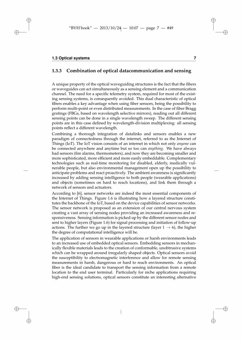
ii
“BVH˙book” — 2013/10/24 — 10:07 — page 7 — #49 ii
ii
ii
1.3 Optical systems 7
1.3.3 Combination of optical datacommunication and sensing
A unique property of the optical waveguiding structures is the fact that the fibersor waveguides can act simultaneously as a sensing element and a communicationchannel. The need for a specific telemetry system, required for most of the exist-ing sensing systems, is consequently avoided. This dual characteristic of opticalfibers enables a key advantage when using fiber sensors, being the possibility toperform multi-point or even distributed measurements. In the case of fiber Bragggratings (FBGs, based on wavelength selective mirrors), reading out all differentsensing points can be done in a single wavelength sweep. The different sensingpoints are in this case defined by wavelength-division multiplexing: all sensingpoints reflect a different wavelength.Combining a thorough integration of datalinks and sensors enables a newparadigm of connectedness through the internet, referred to as the Internet ofThings (IoT). The IoT vision consists of an internet in which not only anyone canbe connected anywhere and anytime but so too can anything. We have alwayshad sensors (fire alarms, thermometers), and now they are becoming smaller andmore sophisticated, more efficient and more easily embeddable. Complementarytechnologies such as real-time monitoring for disabled, elderly, medically vul-nerable people, but also environmental management open up the possibility toanticipate problems and react proactively. The ambient awareness is significantlyincreased by adding sensing intelligence to both people (wearable applications)and objects (sometimes on hard to reach locations), and link them through anetwork of sensors and actuators.According to [6], sensor networks are indeed the most essential components ofthe Internet of Things. Figure 1.6 is illustrating how a layered structure consti-tutes the backbone of the IoT, based on the device capabilities of sensor networks.The sensor network is proposed as an extension of our central nervous systemcreating a vast array of sensing nodes providing an increased awareness and re-sponsiveness. Sensing information is picked up by the different sensor nodes andsent to higher layers (Figure 1.6) for signal processing and initiation of follow-upactions. The further we go up in the layered structure (layer 1 → 6), the higherthe degree of computational intelligence will be.The application of sensors in wearable applications or harsh environments leadsto an increased use of embedded optical sensors. Embedding sensors in mechan-ically flexible materials leads to the creation of conformable, unobtrusive systemswhich can be wrapped around irregularly shaped objects. Optical sensors avoidthe susceptibility to electromagnetic interference and allow for remote sensingmeasurements in harsh, dangerous or hard to reach environments. An opticalfiber is the ideal candidate to transport the sensing information from a remotelocation to the end user terminal. Particularly for niche applications requiringhigh-end sensing solutions, optical sensors constitute an interesting alternative
ii
“BVH˙book” — 2013/10/24 — 10:07 — page 8 — #50 ii
ii
ii
8 General introduction
Figure 1.6 – Layered structure based on the device capabilities of a sensor network. In IoT,this layered architecture may have additional number of sub layers. Schematic diagram
from Perera et al. [6].
outperforming their electrical counterparts despite their higher cost.The polymer embedding approach is discussed in the next section. Integratingoptical sensors in polymer embedding materials leads to the creation of photonicskins, discussed in Section 1.5.
1.4 Polymer embedding
As discussed earlier, the development of miniaturized sensor elements to mea-sure physical properties such as pressure, temperature and the proximity to otherobjects is becoming increasingly important. This evolution has been set forwardowing to the emergence of Microelectromechanical Systems (MEMS) [7]. Thistechnology typically relies on Integrated Circuit (IC) fabrication processes usingrigid substrates such as silicon and glass wafers.The fabrication of sensors on flexible substrates offers several advantages andopens up a broad range of new applications within the field of robotics and wear-able applications. Mounting rigid MEMS based sensors on flexible carriers andconsequently creating rigid islands on a larger flexible substrate is an option toaccomplish this. Fabricating sensor foils to cover large areas is however difficultin terms of connectivity and reliability. Alternatively, one can remove (part of)the rigid carriers of the sensors after mounting on the flexible carriers by etch-ing. This process is however relying on IC fabrication technology, increasing thesystem cost to cover large areas.The idea of sensitive skin was introduced at the 1999 NSF-DARPA Sensitive SkinWorkshop [8]. The main technological challenges were identified as:

ii
“BVH˙book” — 2013/10/24 — 10:07 — page 9 — #51 ii
ii
ii
1.5 Photonic skins 9
• The need for a carrier substrate of the sensors, which is compliant, and de-forms with the object onto/into which it is integrated.
• The need to integrate a vast number of sensing elements onto this carrier.If these sensors are electrically wired, this generates serious challenges inmassive interconnection technology and parallel signal processing capabil-ity.
Later on, a sensitive skin was defined as a large-area, flexible array of sensors withdata processing capabilities, which can be used to cover the entire surface of a machine oreven a part of a human body [9]. Within the same article, a first example of this con-cept was presented (Figure 1.7) containing 64 active infrared sensor pairs (LED &detector), each of which can sense objects within a narrow cone at a distance upto about 20 cm.
Figure 1.7 – The first sensitive skin module: 64 infrared sensor pairs on a Kapton substratewith a distance between neighboring pairs of 25 mm. Courtesy of V. Lumelsky, Robotics
Laboratory, University of Wisconsin-Madison.
Over the last decade, significant progress has been made towards stretchableskin-like structures with embedded sensing features, mainly using flexible elec-tronics leading to so-called e-skins. These skins are typically applied directly ontop of a human skin [10]. Optical skin-like sensing alternatives are discussed inthe next paragraph entailing several advantages such as chemical inertness, im-munity to electromagnetic interference, distributed sensing possibilities and com-patibility with harsh (high temperature and/or pressure) environments.
1.5 Photonic skins
In Figure 1.8, the concept of a photonic skin is presented. A photonic skin is apolymer, mechanically flexible or stretchable, sensing foil consisting of embed-

ii
“BVH˙book” — 2013/10/24 — 10:07 — page 10 — #52 ii
ii
ii
10 General introduction
ded optical sensors resulting in unobtrusive optical sensing systems. Dependingon the envisaged application, this sensing system can provide high-density andhighly accurate measurements on local thermomechanical properties or large-area measurements of ambient parameters.
I i f ( ) l i hiIntegration of (opto-)electronic chips
Integration of coupling structures
Concept from EU-FP7 project
Integration of (multiplexed) fiber sensors
© IMEC 2011 / CONFIDENTIAL
Figure 1.8 – Phosfos (Photonic skins for optical sensing) concept picture.
Optoelectronic and electronic chips are integrated using bare die chip compo-nents leading to ultra-small electrical and optical driving units. The dimen-sions and according mechanical properties of the photonic skin are consequentlylargely determined by the polymer embedding material properties. Although al-ternative optical sensors will be introduced in Chapter 2 and further discussedin Chapter 7, a photonic skin typically relies on optical fiber sensor technology.A crucial technology heavily influencing the reliability and usability of the sens-ing system is therefore the fiber coupling of optoelectronic components to opticalfiber(s). All technology blocks developed within this PhD dissertation need tobe “skin compliant”, i.e. compatible with unobtrusive, planar, mechanicallyflexible sensing skins with limited dimensions (especially thickness).A wide range of applications can be targeted with this photonic sensing skinparadigm. Two potential application domains are illustrated in Figure 1.9:
• One of the domains that could benefit from the photonic sensing skins issituated in the field of robotics. We have for example demonstrated theuse of such a sensing foil with a social pet-like robot (Figure 1.9a) that isdeveloped at the Vrije Universiteit Brussel. The fiber sensor consists of 4 or

ii
“BVH˙book” — 2013/10/24 — 10:07 — page 11 — #53 ii
ii
ii
1.6 Problem statement and objectives 11
more wavelength-multiplexed FBG sensors (red dots in Figure 1.9a). Thissensing concept clearly shows the possibility to integrate different sensingpoints in one optical fiber. Through a meandering fiber embedding design,a large-area pressure sensitive surface can be created.
• Monitoring vital human functions such as breathing movements, heartbeat,blood pressure is a second example of a photonic skin-like sensing applica-tion. Figure 1.9b is depicting a concept picture of a polymer embedded res-piration monitoring vest based on a fiber Bragg grating to visualize breath-ing movements. Important challenges for these wearable applications in-clude weight, size, safety and user friendliness.
(a) An FBG based sensing skin applied to a social pet-type robot [11].
(b) Optical respiratory monitoring applica-tion based on a conformable polymer embed-
ded sensing foil.
Figure 1.9 – Examples of photonic skins for optical sensing.
A more elaborate overview of state-of-the-art photonic skin applications is de-scribed in Chapter 2, Section 2.4. Looking back to the advantages of optical (fiber)sensors described in Section 1.3.3, an important trade-off has to be consideredrelated to the photonic skin concept. The more compact the optical sensing sys-tem is, the closer the optoelectronic driving and read-out components will be tothe optical sensing elements. Important advantages related to the optical sen-sors, such as the possibility to deploy them in harsh environments, may becomevoid because of the vulnerability of these driving and coupling components em-bedded in close vicinity to the sensing devices. Depending on the applicationdomain, one has to decide on the level of integration of the optoelectronic and(fiber) coupling parts.
1.6 Problem statement and objectives
State-of-the-art research has lead to significant progress on all the areas men-tioned in the above discussion. The following specific objectives are definedwithin the scope of this PhD dissertation:

ii
“BVH˙book” — 2013/10/24 — 10:07 — page 12 — #54 ii
ii
ii
12 General introduction
• Polymer fiber embedding Broaden the application domain of fiber sensors byworking towards mechanically flexible and stretchable, typically polymerbased, sensor host materials. Combining these materials with optical fibersensors results in a photonic skin for optical sensing.
Maintaining the sensing functionality of the fiber sensors after embeddingis an important prerequisite. Depending on the sensor type and the em-bedding process, this might be a serious challenge. Accurate control on thefiber position in the sensing skin, both lateral and transversal, is a secondobjective within this task. The level of design flexibility is an important pa-rameter to monitor during the fiber embedding research work. Thoroughcharacterization of the sensing skins in terms of responsivity, sensitivity andsensing range, is an essential third objective.
• Integration and coupling of optoelectronic chips By miniaturizing and integrat-ing optoelectronic (OE) components on a chip level, ultra-small laser anddetector packages are created. These packages can be fiber-coupled whenusing them in combination with optical fiber sensors or serve as stand-alonesensing units (intrinsic sensor).
Commercially available optoelectronic chips typically have a thickness >100 µm. The targeted thickness of an ultra-small package is 40 µm. Thin-ning of optoelectronic components (down to 20 µm) while maintaining theirelectrical and optical properties is therefore a first objective related to opto-electronic integration resulting in mechanically flexible optoelectronic pack-ages. A photonic skin typically has a total thickness of 1 mm or less. Stan-dard fiber coupling techniques immediately compromise this unobtrusivephotonic skin concept. The fabrication of flat, skin compatible, optical cou-pling parts is therefore a second objective.
• Simple and cost-effective optical sensor interrogation systems By simplifying anddownsizing the sensing interrogation schemes, the usability and applicabil-ity of optical sensors can significantly increase.
Combining optoelectronic components on a chip level into a functional in-terrogation system with a state-of-the-art measurement accuracy and reso-lution is one of the most important challenges within this dissertation. Theability to perform full spectral measurements when reading out optical fibersensors, not limited to peak tracking, will enable a unique selling point ofthis embedded interrogation system.
• Ultra-small integrated pressure sensors A sensing alternative for highly accu-rate pressure measurements can be based on self-mixing interferometry in alaser consequently avoiding fiber sensors, coupling structures and photode-tectors. By pushing the limits of the optoelectronic integration process, onecan include the necessary polymer transducer layers and reflective coatings.

ii
“BVH˙book” — 2013/10/24 — 10:07 — page 13 — #55 ii
ii
ii
1.7 Research trajectory and dissertation structure 13
Starting from the embedded optoelectronic components, a first challengeis to integrate a polymer transducer layer converting an externally appliedpressure into a displacement variation. Both the mechanical and optical pa-rameters have to be investigated in order to enable reliable pressure mea-surement based on this optical feedback mechanism. The sensor build-uphas to be optimized in order to combine the packaging, sensing and reflec-tion layers in a proper way in terms of alignment, adhesion, stress concen-trations etc.
Two proof-of-concept optical sensing systems will be described in this disserta-tion:
• An ultra-small integrated optical fiber sensing system.
• A photonic incremental pressure sensor based on optical feedback in a poly-mer embedded Vertical-Cavity Surface-Emitting Laser (VCSEL).
1.7 Research trajectory and dissertation structure
Within the Centre for Microsystems Technology (CMST) research group, the op-tical sensing research topic is tackled in different ways. Based on the particularneeds of the application in terms of ambient parameters, size, sensitivity, rangeetc., a specific sensing principle and according measuring system is selected. Wecan distinguish respectively fiber based, waveguide based and optoelectronicbased sensing systems.Fiber based sensing systems can operate in harsh environments and allow forremote and (quasi-)distributed sensing. Waveguide based sensors can performhigh-density tactile measurements and can be combined with integrated lasersand detectors. Also the combination of optical waveguides and capillary mi-crofluidic channels is under investigation. The sensing principle within the op-tical waveguide can be based on a change in transmitted light intensity but alsoon wavelength shifts introduced by fluorescence. Optoelectronic based sensorsdo not require additional components for read-out purposes. They are thereforeeasier to integrate and potentially also more cost-effective.In all different approaches, the end goal is to come up with a fully integrated sens-ing system incorporating in- and out-coupling structures as well as the necessaryoptoelectronic and possibly also electronic components. This sensing system isthen typically embedded in a flexible or stretchable polymer host material. Thefirst steps towards fully embedded optoelectronic components and waveguidingstructures were carried out within the PhD framework of Erwin Bosman [12].This concept was proven through a polymer, mechanically flexible optical linkwith datacommunication speeds > 1 Gbps. Therefore, thinned optoelectronic

ii
“BVH˙book” — 2013/10/24 — 10:07 — page 14 — #56 ii
ii
ii
14 General introduction
components were embedded in very thin polymer foils making them ideallysuited for incorporation in flexible or stretchable skin materials, together withoptical sensors. The PhD of Jeroen Missinne [13] resulted in an optoelectronicshear sensor using polymer embedding and transducer materials. Also a tactilepressure sensor was developed based on a changed coupling behavior of poly-mer crossing waveguides. The integration of polymer waveguide sensing struc-tures for gas sensing applications is under investigation in the PhD of SandeepKalathimekkad. A foil based stand-alone sensing platform is the ultimate goalof this research. Finally, the application of optical sensors and integrated cou-pling structures within micro-nano biosystems is part of the PhD of Nuria TeigellBeneitez.This dissertation is divided in 8 chapters and the structure of this book is shown inFigure 1.10. After this General Introduction chapter, a technical introduction to tra-ditional optical sensors, polymer based optical sensors, interrogation techniquesand embedding opportunities is presented in Chapter 2. These “introduction”chapters are followed by 3 subsequent “technology” chapters starting with thepolymer embedding of optical fiber sensors (silica or polymer, step-index or mi-crostructured) in Chapter 3. The technological work related to the miniaturizationand integration of optoelectronic components needed to drive the optical sensorsand read out the sensing information is described in Chapter 4. In order to cou-ple optical fibers to the integrated optoelectronic components, a dedicated fibercoupling technology is developed in Chapter 5.The characterization of the embedded optical fiber sensors is included in Chap-ter 3. Chapter 6 is combining the technology related to both fiber embedding aswell as component integration and fiber coupling into an ultra-small and fullyembedded fiber sensing system based on a highly accurate sensor interrogationprinciple (introduced in Chapter 2). The optoelectronic components can also beused to avoid the need for optical fibers and create an optical sensor intrinsic tothe optoelectronic component (Chapter 7). Finally, the overall conclusion and adiscussion of the future work is described in Chapter 8.
1.8 Research context and related projects
The research leading to this dissertation was performed within the framework ofthe following projects:
• A personal Ph.D grant of the Institute for the Promotion of Innovationthrough Science and Technology in Flanders (IWT-Vlaanderen [14]).
• FAOS (Flexible Artificial Optical Skin) [15]SBO project, funded by the Institute for the Promotion of Innovationthrough Science and Technology in Flanders (IWT-Vlaanderen [14])

ii
“BVH˙book” — 2013/10/24 — 10:07 — page 15 — #57 ii
ii
ii
1.8 Research context and related projects 15
Chapter 1 General introduction
Chapter 2 Introduction to optical sensors and integration technologies
Chapter 3 Integrated optical
fiber sensors
Chapter 4 Integrated OE components
for optical sensors
Chapter 5 Coupling integrated OE
components
Chapter 6 Ultra-compact optical fiber sensing system
Chapter 7 High resolution pressure sensor based on optical feedback in a VCSEL
Chapter 8 Conclusion
System level
Technology level
Figure 1.10 – Structure of this dissertation.
Starting date : January 1, 2007Ending date : December 31, 2010Project coordinator : Prof. Dr. Ir. Peter Van Daele, IMEC - Ghent University/ CMST Microsystems, Technologiepark 914A, B-9052 Zwijnaarde, Belgium
FAOS aimed to develop a new paradigm for flexible optical sensors inte-grated with electronic modules and control circuitry. The many advantagesof optical sensors, and mainly optical fiber sensors, make them very attrac-tive for a wide range of applications. The immunity with regard to EMI(electromagnetic interferences), the resistance to harsh environments, thehigh sensitivity and the possibility in parallelizing the read-out all makethese sensors more useful than their electronic counterparts for automotiveapplications, aviation, robotics and others. The use of these optical sensorshowever always implies the use of a light-source, detectors and electronic

ii
“BVH˙book” — 2013/10/24 — 10:07 — page 16 — #58 ii
ii
ii
16 General introduction
circuitry to be coupled and integrated with these sensors. The coupling ofthese fibers with these light sources and detectors is a critical packagingproblem and as it is well-known that costs for packaging, especially withoptoelectronic components and fiber alignment issues are huge and can riseup to 90 % of the total cost of the module. FAOS delivered a technologythat offers an integrated solution to this issue by allowing the embeddingof light sources, detectors and electronic circuitry inside flexible polymermaterials.
• PHOSFOS (PHotonic Skins For Optical Sensing) [16]European ICT-Project, Framework 7Starting date : April 1, 2008Ending date : August 31, 2011Project coordinator : Prof. Dr. Ir. Francis Berghmans, VUB Vrije UniversiteitBrussel Pleinlaan 2, B-1050 Brussels, Belgium
PHOSFOS implemented new approaches to optical sensing, flexible ma-terials, embedding technologies and integration concepts. The PHOSFOSproject is now completed and several breakthroughs in the field of opticalsensing, flexible materials, embedding technologies and integration con-cepts have been achieved which may be used in a wide range of applica-tions. A first highlight of the research involves the development of a newpressure sensitive and temperature insensitive sensor. A second highlightinvolves Bragg grating sensors in polymer optical fibers. The PHOSFOSconsortium also developed a new low-cost Polymer Optical Fiber (POF)sensor interrogator designed to work with polymer optical fibers. The sen-sor interrogator has been designed to operate at a wavelength around 850nm to match the low loss transmission window of POF and to significantlyreduce component costs. Using this technology a new polymer multi-pointFBG sensor that can measure the pressure in various medical applicationshas been demonstrated. More PHOSFOS results and contact informationcan be obtained on the website of the project http://www.phosfos.eu.An introductory video about the project is available on YouTube: http://www.youtube.com/watch?v=pGpL_icFn1c.
The research will be further developed within the framework of the followingproject:
• SSC (Self Sensing Composites) [17]SBO project, funded by the Institute for the Promotion of Innovationthrough Science and Technology in Flanders (IWT-Vlaanderen [14])Starting date : January 1, 2013Ending date : December 31, 2016

ii
“BVH˙book” — 2013/10/24 — 10:07 — page 17 — #59 ii
ii
ii
1.9 Research dissemination 17
Project coordinator : Dr. Ir. Geert Luyckx, Ghent University / MMS (Me-chanics of Materials and Structures) Technologiepark 903, B-9052 Zwij-naarde, Belgium
The technology required to accurately and continuously monitor all criti-cal material aspects of composites is lacking today. In collaboration withindustrial partners the main limitations of current state-of-the-art monitor-ing systems were identified. The development of sensor systems whichovercome these limitations will create a number of important economic op-portunities. In order to overcome the limitations of the currently existing(embedded) sensor technologies which hinder industrial uptake and lim-its the deployment of composite structures up to their full potential, thisproject will realize several scientific breakthroughs. These breakthroughswill result from the development of optical sensors and deformable elec-tronics with innovative and unprecedented properties and which can be in-tegrated within all types of layered materials, with a primary focus on mon-itoring the structural health of composites during their complete life cycle,i.e. from fabrication to operation. Three sensor techniques are considered:micro-structured optical fiber Bragg gratings, polymer waveguide gratingsin relation with deformable electronics and a capacitive sensor based ondeformable electronics.
1.9 Research dissemination
1.9.1 Journal papers
• E. Bosman, G. Van Steenberge, B. Van Hoe, J. Missinne, J. Vanfleteren, andP. Van Daele, “Highly reliable flexible active optical links,” IEEE PHOTON-ICS TECHNOLOGY LETTERS, vol. 22, no. 5, pp. 287–289, 2010. [Online].Available: http://dx.doi.org/10.1109/LPT.2009.2038797
• E. Bosman, J. Missinne, B. Van Hoe, G. Van Steenberge, S. Kalathimekkad,J. Van Erps, I. Milenkov, K. Panajotov, T. Van Gijseghem, P. Dubruel,H. Thienpont, and P. Van Daele, “Ultrathin optoelectronic device pack-aging in flexible carriers,” IEEE JOURNAL OF SELECTED TOPICS INQUANTUM ELECTRONICS, vol. 17, no. 3, pp. 617–628, 2011. [Online].Available: http://dx.doi.org/10.1109/JSTQE.2010.2096407
• J. Missinne, E. Bosman, B. Van Hoe, G. Van Steenberge, S. Kalathimekkad,P. Van Daele, and J. Vanfleteren, “Flexible shear sensor based on embeddedoptoelectronic components,” IEEE PHOTONICS TECHNOLOGY LETTERS,vol. 23, no. 12, pp. 771–773, 2011. [Online]. Available: http://dx.doi.org/10.1109/LPT.2011.2134844

ii
“BVH˙book” — 2013/10/24 — 10:07 — page 18 — #60 ii
ii
ii
18 General introduction
• B. Van Hoe, E. Bosman, J. Missinne, S. Kalathimekkad, G. Melpignano,T. De Geyter, G. Godier, P. Van Daele, and G. Van Steenberge, “Photonicincremental pressure sensor based on optical feedback in a polymer embed-ded vcsel,” IEEE PHOTONICS TECHNOLOGY LETTERS, vol. 24, no. 13, pp.1151–1153, 2012. [Online]. Available: http://dx.doi.org/10.1109/LPT.2012.2197678
• B. Van Hoe, G. Lee, E. Bosman, J. Missinne, S. Kalathimekkad, O. Maskery,D. J. Webb, K. Sugden, P. Van Daele, and G. Van Steenberge, “Ultra smallintegrated optical fiber sensing system,” SENSORS, vol. 12, no. 9, pp.12 052–12 069, 2012. [Online]. Available: http://dx.doi.org/10.3390/s120912052
• J. Missinne, E. Bosman, B. Van Hoe, R. Verplancke, G. Van Steenberge,S. Kalathimekkad, P. Van Daele, and J. Vanfleteren, “Two axis optoelectronictactile shear stress sensor,” SENSORS AND ACTUATORS A-PHYSICAL,vol. 186, pp. 63–68, 2012. [Online]. Available: http://dx.doi.org/10.1016/j.sna.2012.01.038
1.9.2 Proceedings of international conferences, with Web of Sci-ence indexation
• J. Missinne, G. Van Steenberge, B. Van Hoe, K. Van Coillie, T. Van Gi-jseghem, P. Dubruel, J. Vanfleteren, and P. Van Daele, “An array waveguidesensor for artificial optical skins,” in Proceedings of SPIE, the International So-ciety for Optical Engineering, A. Glebov and R. Chen, Eds., vol. 7221. SPIE,the International Society for Optical Engineering, 2009. [Online]. Available:http://dx.doi.org/10.1117/12.809154
• E. Ferraris, T. Van Gijseghem, C. Yan, B. Van Hoe, G. Van Steenberge,P. Van Daele, P. Dubruel, and D. Reynaerts, “Embedding of fibre optic sen-sors within flexible host,” in 4M/ICOMM 2009 - THE GLOBAL CONFER-ENCE ON MICRO MANUFACTURE. Professional Engineering Publishingltd, 2009, pp. 351–354.
• X. Chen, C. Zhang, D. J. Webb, B. Van Hoe, G. Van Steenberge, K. Kalli,F. Berghmans, H. Thienpont, W. Urbanczyk, K. Sugden, and G.-D. Peng,“Polymer photonic sensing skin,” in Proceedings of SPIE, the International So-ciety for Optical Engineering, J. L. s. Santos, B. Culshaw, J. M. Lo pez Higuera,and W. N. MacPherson, Eds., vol. 7653. SPIE, the International Society forOptical Engineering, 2010. [Online]. Available: http://dx.doi.org/10.1117/12.866367
• E. Bosman, J. Bauwelinck, K. Panajotov, G. Van Steenberge, J. Missinne,B. Van Hoe, and P. Van Daele, “Characterization of flexible fully embed-

ii
“BVH˙book” — 2013/10/24 — 10:07 — page 19 — #61 ii
ii
ii
1.9 Research dissemination 19
ded optical links,” in Proceedings of SPIE, the International Society for OpticalEngineering, H. Thienpont, P. Van Daele, J. Mohr, and H. Zappe, Eds., vol.7716. SPIE, the International Society for Optical Engineering, 2010. [On-line]. Available: http://dx.doi.org/10.1117/12.854229
• J. Missinne, G. Van Steenberge, B. Van Hoe, E. Bosman, C. Debaes, J. r.Van Erps, C. Yan, E. Ferraris, P. Van Daele, J. Vanfleteren, H. Thienpont, andD. Reynaerts, “High density optical pressure sensor foil based on arrays ofcrossing flexible waveguides,” in Proceedings of SPIE, the International Societyfor Optical Engineering, H. Thienpont, P. Van Daele, J. Mohr, and H. Zappe,Eds., vol. 7716. SPIE, the International Society for Optical Engineering,2010. [Online]. Available: http://dx.doi.org/10.1117/12.854578
• X. Chen, C. Zhang, B. Van Hoe, D. J. Webb, K. Kalli, G. Van Steenberge, andG.-D. Peng, “Photonic skin for pressure and strain sensing,” in PROCEED-INGS OF SPIE - THE INTERNATIONAL SOCIETY FOR OPTICAL ENGI-NEERING, F. Berghmans, A. G. Mignani, and C. A. van Hoof, Eds., vol.7726, no. Optical Sensing and Detection. SPIE, the International Societyfor Optical Engineering, 2010. [Online]. Available: http://dx.doi.org/10.1117/12.854235
• B. Van Hoe, G. Van Steenberge, E. Bosman, J. Missinne, T. Geernaert,F. Berghmans, D. J. Webb, and P. Van Daele, “Optical fiber sensors em-bedded in polymer flexible foils,” in Proceedings of SPIE, the InternationalSociety for Optical Engineering, F. Berghmans, A. G. Mignani, and C. A.van Hoof, Eds., vol. 7726, no. Optical sensing and detection. SPIE, theInternational Society for Optical Engineering, 2010. [Online]. Available:http://dx.doi.org/10.1117/12.854865
• E. Bosman, G. Van Steenberge, J. Missinne, B. Van Hoe, and P. Van Daele,“Packaging of opto-electronic devices for flexible applications,” in Proceed-ings of SPIE, the International Society for Optical Engineering, A. L. Glebov andR. T. Chen, Eds., vol. 7607. SPIE, the International Society for Optical Engi-neering, 2010. [Online]. Available: http://dx.doi.org/10.1117/12.841553
• B. Van Hoe, D. Lamon, E. Bosman, G. Van Steenberge, J. Missinne, P.Goethals, P. Krassimir, D. Reynaerts, J. Vanfleteren, and P. Van Daele, “Em-bedded high resolution sensor based on optical feedback in a vertical cavitysurface emitting laser,” in Proceedings of SPIE, the International Society for Op-tical Engineering, K. J. Peters, W. Ecke, and T. E. Matikas, Eds., vol. 7648.SPIE, the International Society for Optical Engineering, 2010. [Online].Available: http://dx.doi.org/10.1117/12.847647
• J. Missinne, E. Bosman, B. Van Hoe, G. Van Steenberge, P. Van Daele, andJ. Vanfleteren, “Embedded flexible optical shear sensor,” in IEEE Sensors.

ii
“BVH˙book” — 2013/10/24 — 10:07 — page 20 — #62 ii
ii
ii
20 General introduction
IEEE, 2010, pp. 987–990. [Online]. Available: http://dx.doi.org/10.1109/ICSENS.2010.5690919
• F. Berghmans, T. Geernaert, S. Sulejmani, H. Thienpont, G. Van Steenberge,B. Van Hoe, P. Dubruel, W. Urbanczyk, P. Mergo, D. J. Webb, K. Kalli,J. Van Roosbroeck, and K. Sugden, “Photonic crystal fiber bragg gratingbased sensors: opportunities for applications in healthcare,” in Proceedingsof SPIE, the International Society for Optical Engineering, J. Popp, D. Matthews,J. Tian, and C. Yang, Eds., vol. 8311. SPIE, the International Society for Op-tical Engineering, 2011. [Online]. Available: http://dx.doi.org/10.1117/12.901240
• E. Bosman, G. Van Steenberge, J. Missinne, B. Van Hoe, S. Kalathimekkad,and P. Van Daele, “Packaging technology enabling flexible optical intercon-nections,” in Proceedings of SPIE, the International Society for Optical Engi-neering, A. L. Glebov and R. T. Chen, Eds., vol. 7944. SPIE, the Interna-tional Society for Optical Engineering, 2011. [Online]. Available: http://dx.doi.org/10.1117/12.874959
• B. Van Hoe, E. Bosman, J. Missinne, G. Van Steenberge, P. Van Daele,W. Zhang, I. Johnson, K. Sugden, D. J. Webb, and K. Kalli, “Embeddedmultiplexed polymer optical fiber sensor for esophageal manometry,” in2011 IEEE Sensors. IEEE, 2011, pp. 1499–1502. [Online]. Available:http://dx.doi.org/10.1109/ICSENS.2011.6127216
• S. Kalathimekkad, J. Missinne, J. D. Arias Espinoza, B. Van Hoe, E. Bosman,E. Smits, R. Mandamparambil, G. Van Steenberge, and J. Vanfleteren,“Fluorescence-based optochemical sensor on flexible foils,” in PROCEED-INGS OF SPIE, THE INTERNATIONAL SOCIETY FOR OPTICAL ENGI-NEERING, F. Berghmans, A. G. Mignani, and P. De Moor, Eds., vol. 8439,no. 0Y-1. SPIE, 2012, pp. 84 390Y–1–84 390Y–9. [Online]. Available:http://dx.doi.org/10.1117/12.922663
• B. Van Hoe, E. Bosman, J. Missinne, S. Kalathimekkad, G. Lee, Z. Yan,K. Sugden, D. Webb, G. Van Steenberge, and P. Van Daele, “Low-cost fullyintegrated fiber bragg grating interrogation system,” in PROCEEDINGSOF SPIE, THE INTERNATIONAL SOCIETY FOR OPTICAL ENGINEERING,J. Canning and G. Peng, Eds., vol. 8351. SPIE-INT SOC OPTICAL ENGI-NEERING, 2012. [Online]. Available: http://dx.doi.org/10.1117/12.914253
• S. Kalathimekkad, J. Missinne, J. D. Arias Espinoza, B. Van Hoe, E. Bosman,E. Smits, R. Mandamparambil, G. Van Steenberge, and J. Vanfleteren, “Foil-based optical technology platform for optochemical sensors,” in PROCEED-INGS OF SPIE, THE INTERNATIONAL SOCIETY FOR OPTICAL ENGI-NEERING, J. E. Broquin and G. N. Conti, Eds., vol. 8264, no. 0R-1. Spie,

ii
“BVH˙book” — 2013/10/24 — 10:07 — page 21 — #63 ii
ii
ii
1.9 Research dissemination 21
2012, pp. 82 640R–1–82 640R–9. [Online]. Available: http://dx.doi.org/10.1117/12.908182
• B. Van Hoe, E. Bosman, J. Missinne, S. Kalathimekkad, G. Van Steenberge,and P. Van Daele, “Novel coupling and packaging approaches for optical in-terconnects (invited paper),” in PROCEEDINGS OF SPIE, THE INTERNA-TIONAL SOCIETY FOR OPTICAL ENGINEERING, A. Glebov and R. Chen,Eds., vol. 8267. SPIE-INT SOC OPTICAL ENGINEERING, 2012. [Online].Available: http://dx.doi.org/10.1117/12.913760
• G. C. Lee, B. Van Hoe, Z. Yan, O. Maskery, K. Sugden, D. Webb, andG. Van Steenberge, “A compact, portable and low cost generic interro-gation strain sensor system using an embedded vcsel, detector and fibrebragg grating,” in PROCEEDINGS OF SPIE, THE INTERNATIONAL SO-CIETY FOR OPTICAL ENGINEERING, K. Choquette and C. Lei, Eds., vol.8276. SPIE-INT SOC OPTICAL ENGINEERING, 2012. [Online]. Available:http://dx.doi.org/10.1117/12.907810
• J. Missinne, E. Bosman, B. Van Hoe, R. Verplancke, G. Van Steenberge,S. Kalathimekkad, P. Van Daele, and J. Vanfleteren, “Ultra thin optical tac-tile shear sensor,” in PROCEDIA ENGINEERING, G. Kaltsas and C. Tsamis,Eds., vol. 25. Elsevier Science, 2012, pp. 1393–1396. [Online]. Available:http://dx.doi.org/10.1016/j.proeng.2011.12.344
1.9.3 Proceedings of international conferences, without Web ofScience indexation
• G. Van Steenberge, E. Bosman, J. Missinne, B. Van Hoe, and P. Van Daele,“Flexible optical interconnects,” in Proceedings of the 2nd International Sym-posium on Photonic Packaging, 2008.
• E. Bosman, B. Van Hoe, J. Missinne, G. Van Steenberge, S. Kalathimekkad,and P. Van Daele, “Unobtrusive packaging of optoelectronic devices foroptical tactile and shear sensors,” in PROCEEDINGS OF THE 5TH IN-TERNATIONAL CONFERENCE ON SENSING TECHNOLOGY. IEEE,2011, pp. 504–509. [Online]. Available: http://dx.doi.org/10.1109/ICSensT.2011.6137031
• D. Barrera, I.P. Johnson, D.J. Webb, B. Van Hoe, G. Van Steenberge, andS. Sales, “Dynamic Strain Sensor using a VCSEL and a Polymer Fiber BraggGrating in a Multimode Fiber,” in 20th International Conference on PolymerOptical Fibers, Bilbao, Spain. 2011.
• J. Missinne, B. Van Hoe, E. Bosman, S. Kalathimekkad, G. Van Steenberge,and P. Van Daele, “Compact coupling and packaging concepts for flexi-

ii
“BVH˙book” — 2013/10/24 — 10:07 — page 22 — #64 ii
ii
ii
22 General introduction
ble and stretchable polymer optical interconnects,” in 2012 IEEE OpticalInterconnects Conference. IEEE, 2012, pp. 129–130. [Online]. Available:http://dx.doi.org/10.1109/OIC.2012.6224412
• T. Geernaert, C. Sonnenfeld, S. Sulejmani, T. Baghdasaryan, G. Van Steen-berge, B. Van Hoe, P. Mergo, W. Urbanczyck, M. Becker, F. Berghmans, andH. Thienpont, “Towards flexible photonic sensing skins with optical fibersensors,” in 2012 4th IEEE RAS & EMBS International Conference on Biomed-ical Robotics and Biomechatronics (BioRob 2012). IEEE, 2012, pp. 628–633.[Online]. Available: http://dx.doi.org/10.1109/BioRob.2012.6290767
1.9.4 Other international conferences, without proceedings
• G. Van Steenberge, J. Missine, B. Van Hoe, K. Van Coillie, J. Vanfleteren, andP. Van Daele, “Array waveguide sensor,” in Proceedings NEMO ScientificGeneral Networking Meeting, 2008.
• E. Bosman, B. Van Hoe, J. Missinne, G. Van Steenberge, and P. Van Daele,“Packaging of flexible optical interconnections,” in International Conferenceon Micro and Nano Engineering, 35th, Ghent, Belgium. 2009.
• B Van Hoe, “Phosfos Embedding Technology for Integrated Sensing Solu-tions” in European Commission 4th Concertation meeting on Photonics EnabledApplications, Athens, Greece. 2009.
• C. Sonnenfeld, S. Sulejmani, T. Geernaert, F. Berghmans, H. Thienpont,N. Lammens, G. Luyckx, E. Voet, J. Degrieck, B. Van Hoe, G. Van Steen-berge, P. Van Daele, W. Urbanczyk, J. Wojcik, M. Becker, and H. Bartelt,“Capteurs a fibre optique pour materiaux composites et polymeres intelli-gents,” in Methodes et Techniques Optiques pour l’Industrie, Toulouse, France.2010.
• B. Van Hoe, “Phosfos Integration Technology,” in Phosfos Industrial UserClub Meeting, part of INDUSTRY MEETS ACADEMIA - SPIE OPTICALMETROLOGY, Munchen, Germany. 2011.
• B. Van Hoe, “Photonic Skins for Optical Sensing,” in 3rd Flexible & Stretch-able Electronics Workshop, Berlin, Germany. 2011.
1.9.5 Proceedings of national conferences
• J. Missinne and B. Van Hoe, “Array waveguide sensor for artificial opticalskin,” in UGent-FirW Doctoraatssymposium, 9e. Universiteit Gent. FaculteitIngenieurswetenschappen, 2008, pp. 202–203.

ii
“BVH˙book” — 2013/10/24 — 10:07 — page 23 — #65 ii
ii
ii
1.9 Research dissemination 23
• B. Van Hoe and D. Lamon, “Embedded high resolution sensor based onoptical feedback in vertical cavity surface emitting laser,” in UGent-FirWDoctoraatssymposium, 10e. Universiteit Gent. Faculteit Ingenieursweten-schappen, 2009.
• B. Van Hoe, “Embedded fiber sensors with ultra-compact read-out,” inFEA PhD symposium, 12th. Ghent University. Faculty of Engineer-ing and Architecture, 2011, pp. 100–100. [Online]. Available: http://symposium.fea.ugent.be/sites/symposium.elis.ugent.be/files/phdsymposium/submission932_poster.pdf
1.9.6 Other publications
• B. Van Hoe, “Ontwikkeling van een artificial optical skin”, Ugent MasterThesis, 2007. [Online]. Available: http://lib.ugent.be/fulltxt/RUG01/001/312/340/RUG01-001312340_2010_0001_AC.pdf
• B. Van Hoe, K. Van Coillie, G. Van Steenberge, J. Vanfleteren, and P. VanDaele, “Nieuwe benadering voor druksensoren: flexibele artificiele optis-che huid,” KVIV Ingenieursprijzen, 2009.
• J. Missinne, B. Van Hoe, “Artificial skin based on flexible optical tactile sen-sors,” in SPIE newsroom, Jan 2010. [Online]. Available: http://spie.org/x38859.xml?ArticleID=x38859
• B. Van Hoe, “Paving the way towards ultra-compact fiber sensing systems,”in Cohesi Sensors of the Future Symposium, Leuven, Belgium. 2012.
1.9.7 Exhibitions and demonstrations
The technology developed within this dissertation has been demonstrated duringfollowing exhibitions:
• E. Bosman, J. Missinne, B. Van Hoe, P. Geerinck, and G. Van Steenberge,“Photonics in Motion - Stretchable optical waveguides”, European Photon-ics Innovation Village 2010, Brussels, Belgium.Best Innovation by a Multilateral Project, Organisation or CompanyAward: 1st Runner-up.
• Phosfos, “Light feels pressure”, European Commission Innovation Con-vention 2011, Brussels, Belgium. http://ec.europa.eu/research/innovation-union/ic2011/index_en.cfm.
• J. Missinne, B. Van Hoe, S. Kalathimekkad, E. Bosman, and G. Van Steen-berge, “Flexible Photonics feel it, smell it...bend it!”, Cohesi Sensors of the

ii
“BVH˙book” — 2013/10/24 — 10:07 — page 24 — #66 ii
ii
ii
24 General introduction
Future Symposium 2012, Imec Leuven, Belgium. http://www.cohesi.be/.
1.9.8 The following patent has been filed
• G. Van Steenberge, J. Missinne, E. Bosman and B. Van Hoe, “Optical shearsensor and method of producing such an optical shear sensor,” World-wide patent, WO/2011/128266 A1, 20 October 2011 and US publication,US/2013/0036829 A1, 14 February 2013.

ii
“BVH˙book” — 2013/10/24 — 10:07 — page 25 — #67 ii
ii
ii
References 25
References
[1] T. Geernaert, “Microstructured fiber bragg grating sensors: From fiber de-sign to sensor implementation,” Ph.D. dissertation, Vrije Universiteit Brus-sel, 2011.
[2] I-Micronews. (Accessed 2013) “omnivision readies for wafer level cameracube production”. [Online]. Available: http://www.i-micronews.com/lectureArticle.asp?id=2723
[3] I. Moellers, D. Jaeger, R. Gaudino, A. Nocivelli, H. Kragl, O. Ziemann,N. Weber, T. Koonen, C. Lezzi, A. Bluschke, and S. Randel, “Plastic opticalfiber technology for reliable home networking: Overview and results of theeu project pof-all,” IEEE Communications Magazine, vol. 47, no. 8, pp. 58–68,Aug. 2009.
[4] H. Ma, A. Jen, and L. Dalton, “Polymer-based optical waveguides: Materi-als, processing, and devices,” Advanced Materials, vol. 14, no. 19, pp. 1339–1365, Oct. 2002.
[5] L. Eldada and L. Shacklette, “Advances in polymer integrated optics,” IEEEJournal of Selected Topics in Quantum Electronics, vol. 6, no. 1, pp. 54–68, 2000.
[6] C. Perera, A. Zaslavsky, P. Christen, and D. Georgakopoulos, “Context awarecomputing for the internet of things: A survey,” IEEE Communications Sur-veys & Tutorials, accepted for publication, pp. 1–41, 2013.
[7] W. Eaton and J. Smith, “Micromachined pressure sensors: Review and recentdevelopments,” Smart Materials & Structures, vol. 6, no. 5, pp. 530–539, Oct.1997.
[8] V. Lumelsky, M. Shur, and S. Wagner, “Sensitive skin workshop,” NSF,DARPA Sensitive Skin Workshop Report, pp. 1–129, Oct. 1999, arlington, Vir-ginia.
[9] V. Lumelsky, M. Shur, and S. Wagner, “Sensitive skin,” Sensors Journal, IEEE,vol. 1, no. 1, pp. 41–51, June 2001.
[10] T. Someya, “Bionic skin for a cyborg you - flexible electronics allow us tocover robots and humans with stretchy sensors,” IEEE Spectrum, Aug. 2013.
[11] Probo, a huggable robotic friend. (Accessed 2013) Project website. [Online].Available: http://probo.vub.ac.be/
[12] E. Bosman, “Integration of optical interconnections and opto-electronic com-ponents in flexible substrates,” Ph.D. dissertation, Ghent University, 2010.

ii
“BVH˙book” — 2013/10/24 — 10:07 — page 26 — #68 ii
ii
ii
26 General introduction
[13] J. Missinne, “Development of conformable optical and optoelectronic basedtactile sensors,” Ph.D. dissertation, Ghent University, 2011.
[14] IWT. (Accessed 2012) Flemisch institute for the promotion of innovation byscience and technology (iwt). [Online]. Available: http://www.iwt.be/
[15] FAOS Consortium. (2007) Flexible artificial optical skin (faos). [Online].Available: http://intecweb.intec.ugent.be/faos/
[16] Phosfos Consortium. (2008) Photonic skins for optical sensing. [Online].Available: http://www.phosfos.eu/
[17] SSC Consortium. (2013) Self sensing composites. [Online]. Available:www.selfsensingcomposites.be/

ii
“BVH˙book” — 2013/10/24 — 10:07 — page 27 — #69 ii
ii
ii
2Introduction to optical sensors and
integration technologies
In this chapter, several optical sensor concepts and working principles are introduced aswell as the necessary driving and read-out techniques to interpret the optical sensingsignals. Furthermore, the combination of optical sensors with polymer materials both assensor material and as host material as well as the associated advantages are discussed.The overview presented in this chapter is by no means intended to be a complete list ofthe available optical sensors which can be based on or embedded in polymers. The aimis rather to provide the necessary background information before going into the technicaldetails of the sensor concepts investigated in this dissertation.
2.1 Optical sensor principles
As discussed in the previous chapter, traditional - electrical - sensors for measur-ing physical quantities such as temperature, strain or pressure are mostly basedon electrical working principles such as changing resistance or capacitance. Themain drawbacks of these sensors are related to the sensitivity, cross-talk, non-compatibility with harsh environments and their size. Optical sensors are basedon the interaction between light and the ambient environment, and constitute aninteresting alternative providing several advantages. The field of optical sensorscan be classified according to different characteristics [1].

ii
“BVH˙book” — 2013/10/24 — 10:07 — page 28 — #70 ii
ii
ii
28 Introduction to optical sensors and integration technologies
A first option is the distinction whether the light is propagating in free-space orguided in a waveguiding structure (for example a fiber). A lot of conventionaloptical sensing systems are for example based on free-space interferometry andspectroscopy. Guided-wave sensing adds to the intrinsic advantages of opticalsensing techniques the possibility of guiding the light beam in a confined andinaccessible medium, thus allowing more versatile and less perturbed measure-ments [2].A second possibility is to distinguish to what extent the sensor is distributed.Point sensors can only measure certain measurands at discrete positions whereasdistributed sensors provide continuous spatial measurements. A quasi-distributedmeasurement can be obtained using a combination of several point sensors at dif-ferent locations which can be read out in parallel.As a third option, the sensor working principle can be used to distinguish be-tween the different types of optical sensors. The overview presented in the fol-lowing paragraphs is based on this criterion. A more elaborate overview of thedifferent working principles of (fiber) optic sensors can for example be foundin [3].
2.1.1 Intensity based optical sensors
A first type of sensors are devices with a working principle based on the modu-lation of light intensity. The sensing information is then encoded in a change ofthe optical power (absolute or relative values) which is reflected or transmittedby the sensing medium to an optical photodetecting unit.
Optoelectronic based shear sensor
A second example of an intensity based optical sensor, consists of two optoelec-tronic components facing each other in free-space: one laser source and one de-tector. The working principle is based on the measurement of the light intensitywhich is coupled from the laser to the detector. This is an application using free-space light propagation consequently not requiring coupling of the light into anoptical fiber. When the optoelectronic source and detector are perfectly aligned,the coupled optical power and associated photocurrent in the detector are maxi-mized. Any shift in the alignment of the two components will lead to a decreasein this signal.This intensity based working principle can be used to fabricate a highly accu-rate and sophisticated sensor to measure shear force. Within the PhD researchof Jeroen Missinne [4], an ultra-small and mechanically flexible prototype wasfabricated and characterized. The working principle is shown in Figure 2.1.A Vertical-Cavity Surface-Emitting Laser (VCSEL) and photodiode chip are em-bedded in ultra-thin flexible packages. A polymer polydimethylsiloxane (PDMS)

ii
“BVH˙book” — 2013/10/24 — 10:07 — page 29 — #71 ii
ii
ii
2.1 Optical sensor principles 29
VCSEL chip
photodiode chip
Ultra thin flexible photodiode package
Ultra thin flexible VCSEL package
PDMS transducer layer 180µm
Figure 2.1 – Principle of optical intensity based shear sensor based on changing couplingbehavior between a light source and a detector.
transducer layer is applied between the two packages, aligned on top of eachother and irreversibly bonded. The PDMS layer is a deformable and compress-ible layer converting an applied shear force into a lateral displacement and thuschanging the VCSEL-photodiode optical coupling efficiency. A layer thickness of180 µm is a typical value which was used for the experimental characterization,yielding a maximum shear force sensitivity of −350 µA/N or −7 µA/kPa [5].These responsivity values are varying when changing the thickness of the trans-ducer layer. Tuning the mechanical properties of the transducer layer allows ad-justing the sensor to the needs of a specific application in terms of sensing range,accuracy and responsivity. The size, shape and optical properties (modal proper-ties, wavelength etc.) of the optoelectronic components are also important param-eters influencing the linearity and usefulness for certain applications, requiringfor example multi-directional determination of the applied shear force.This sensing principle has been proven to exhibit only very limited cross-sensitivity to pressure. A major disadvantage of this sensor is the direct depen-dence on optical intensity measurements inevitably entailing challenges relatedto unwanted optical power fluctuations, for example due to optoelectronic ag-ing effects or temperature variations. A possible solution is the use of referencecomponents enabling relative measurements [6].
Distributed optical fiber sensor
The first example is based on light propagation in an optical fiber. An opticalfiber can act simultaneously as optical channel and distributed transducer en-abling distributed measurements along the fiber axis. The fiber can then playthe role of a “nerve” for materials and structures in which the fiber is embed-

ii
“BVH˙book” — 2013/10/24 — 10:07 — page 30 — #72 ii
ii
ii
30 Introduction to optical sensors and integration technologies
ded [7]. The sensing mechanism is in this case inherent to the fiber and basedon light scattering (Rayleigh, Raman and Brillouin scattering). One of the mostpopular intrinsic distributed fiber optic sensors is optical time-domain reflectom-etry based on Rayleigh scattering. A simple example of this sensing principle isschematically shown in Figure 2.2.
continuous sensing fiber
Pulsed
laser
Photodetection
+ Processing
coupler
fiber link
Sensing information on α(z)
optical fiber
Change external
parameter αt
P (t)
t =
log[P (t)]slope s
2 n z
c
slope
s + Δs(α)
z1 z2
z1 z2
z
fiber end
reflection
Figure 2.2 – Principle of optical time-domain reflectometry based on Rayleigh scattering.
P (t) is the optical power, z is the axis along the fiber, n is the refractive index of thefiber and c is the speed of light. When light is launched into an optical fiber, lossesoccur due to Rayleigh scattering that arises as a result of random, microscopic(less than the wavelength of propagated light) variations in the index of refractionof the fiber core. A fraction of the light scattered in a counterpropagation direction(180° relative to the incident direction) is recaptured by the fiber aperture andreturned towards the source [8]. A narrow optical signal emitted by a pulsed laseris launched into the optical fiber (Figure 2.2) and a photodetector is capturingthe reflected light. This photodetector signal is further processed to extract thesensing information. In a specific area along the optical sensing fiber (between z1and z2), an external parameter α is perturbed and the local scattering coefficientis consequently changed. This spatial change can be quantified by analyzing theoptical pulse which is reflected by the fiber. More specifically the slope of thelogarithmic optical power versus time is an indication for the reflection coefficientas a function of distance along the fiber. Comparing the reflected optical intensity

ii
“BVH˙book” — 2013/10/24 — 10:07 — page 31 — #73 ii
ii
ii
2.1 Optical sensor principles 31
with the pulsed laser signal reflects the local fiber status and enables localizationand quantification of the external perturbation. Since this sensing technique isbased on detecting the back-scattered optical signal of the light pulse as a functionof time, this technique is called Optical Time-Domain Reflectometry (OTDR).An elaborate overview of the different opportunities to use optical fibers as dis-tributed sensors including recent trends and developments can be found in [9].
2.1.2 Interferometry based optical sensors
A second type of optical sensors is based on interferometric working principles.In this paragraph interferometry in laser components, allowing for measure-ments not depending on light intensity, is discussed.Laser interferometry is a well-known and widespread technique to measure dis-placement, velocity, vibration and distance. This technique is based on an exter-nal interferometer, an optical transducer consisting of lenses, prisms and mirrorswhich is typically read out by a laser. Popular applications of these techniquesare the Michelson [10] and Mach-Zehnder [11] interferometers. Later, a new tech-nique appeared, in which a fraction of the light back-reflected or back-scatteredby a remote target is allowed to re-enter the laser cavity. The reflected light inter-feres with the light generated inside the laser, generating a modulation of both theamplitude and the frequency of the lasing field. This approach is a special case oflaser interferometry, equivalently called self-mixing, feedback or induced-modulationinterferometry, and is related to the spatial coherence length of the laser [12]. Thelaser source acts as a sensitive detector for the path length 2 k Lext (where k is thewavenumber, and Lext is the target reflector distance) traveled by the light to thetarget and back, exploiting so-called injection-detection [13]. The laser is in thiscase at the same time the optical source and the optical detector.The first demonstrations of this principle used gas lasers to detect the Dopplershift caused by a moving remote reflector [14]. Turning point experiments werethose reporting the first complete self-mixing interferometer/vibrometer [15] andthe use of a Laser Diode (LD) as a source/detector [16]. Remote sensing appli-cations based on the self-mixing effect in low-cost commercial Fabry-Perot (FP)LDs have appeared in the scientific literature since 1986 [16, 17], demonstratingthe feasibility of velocity, distance and displacement measurements [16]-[18].According to Bosch et al. [13], some important advantages of the self-mixing sens-ing scheme are:
• No optical interferometer external to the source is needed, resulting in avery simple, part-count-saving and compact set-up.
• No external photodetector is required, because the signal is provided by themonitor photodiode contained in the LD package.

ii
“BVH˙book” — 2013/10/24 — 10:07 — page 32 — #74 ii
ii
ii
32 Introduction to optical sensors and integration technologies
• The sensitivity of the scheme is very high, being a sort of coherent detectionthat easily attains the quantum detection regime (i.e. sub-nm sensitivity inpath length is possible)
• Successful operation on rough diffusive surfaces can be achieved
• Information is carried by the laser beam and it can be picked up everywhere(also at the remote target location).
A complete analysis of laser diodes with optical feedback can be performed byusing the equations first derived by Lang and Kobayashi [19].A typical optoelectronic source which is used for optical feedback measurementsis a VCSEL. Within this dissertation an incremental pressure sensor is builtbased on this working principle. Starting from polymer embedded VCSELcomponents, polymer sensing layers are added to extend the laser cavity byintroducing a compressible external cavity build-up. A thin metal layer (theexternal target) on top of this external cavity is reflecting a fraction of the emittedlaser light back into the laser cavity. Critical parameters in order to observe self-mixing interferometry useful for sensing measurements are a minimum thresholdoptical power which has to be coupled back into the laser diode cavity and anoptical feedback parameter within the correct range. A detailed discussion onthis integrated VCSEL pressure sensor is provided in Chapter 7.
2.1.3 Bragg reflection based optical sensors
A third type of optical sensors relies on wavelength selective mirrors yieldingwavelength encoded sensor signals. The sensing information has to be extractedfrom a change in the optical wavelength reflected by this mirror, requiring spec-tral analysis and read-out units. The most commonly used type of optical sen-sor based on wavelength encoded information is a fiber sensor based on FiberBragg Gratings (FBGs). Optical fiber sensors are intrinsic sensor devices, refer-ring to the unique feature that the optical fiber is simultaneously sensing elementand communication channel. Therefore, there is no need to consider a specifictelemetry system that is always required in other sensing technologies. Proba-bly more important, this dual characteristic of the optical fiber opens the naturalconsideration of fiber optic sensing networks for multi-point or quasi-distributedmeasurement [20].Within the following sections, the basic principles as well as the most commonfabrication technologies of wavelength selective mirrors - based on Bragg reflec-tion - in optical fibers are discussed.

ii
“BVH˙book” — 2013/10/24 — 10:07 — page 33 — #75 ii
ii
ii
2.1 Optical sensor principles 33
Bragg grating working principle
The working principle of these mirrors is based on a modulation of the local effec-tive refractive index of the optical fiber causing Bragg diffraction. A fiber Bragggrating sensor takes the form of a permanent periodic spatial modulation of therefractive index along the core of an optical fiber, commonly induced using ultra vi-olet light. The reflecting Bragg wavelength is consequently related to the effectiverefractive index of the fiber core neff and the period of the grating structure ΛFBGthrough following Bragg grating condition formula:
m λB = 2 neff ΛFBG
A simple visualization of a fiber Bragg grating is shown in Figure 2.3. A broad-band source is used to couple light into an optical fiber. At the level of the Bragggrating, part of the light is reflected. The Bragg wavelength can be read out inreflection or transmission, respectively looking for a maximum or minimum inthe optical spectrum.
λcentral λ
I
λ
I
Spectral analysis
Transmission
λ
I Reflection
λcentral λcentral
single-mode SLED source
ΛFBG
fiber cladding fiber core
Figure 2.3 – Fiber Bragg grating working principle.
Under the influence of temperature or strain, both the period of the modulationand the mean index of the core mode change, leading to a shift in the reflectedwavelength by this diffractive structure. The strain response arises due to boththe physical elongation of the sensor (and corresponding fractional change ingrating pitch), and the change in fiber index due to photoelastic effects, whereasthe thermal response arises due to the inherent thermal expansion of the fibermaterial and the temperature dependence of the refractive index (thermo-opticeffect). The shift in Bragg wavelength with strain and temperature can be ex-pressed using [21]:

ii
“BVH˙book” — 2013/10/24 — 10:07 — page 34 — #76 ii
ii
ii
34 Introduction to optical sensors and integration technologies
∆λB = 2 neff ∆(
1− neff2
[P12 − ν(P11 + P12)]
ε +
[α +
dneff/dTneff
]∆T)
where ε is the applied strain, Pij are the coefficients of the stress-optic tensor, ν isPoisson’s ratio, α is the Coefficient of Thermal Expansion (CTE) of the fiber ma-terial (e.g. silica), and ∆T is the temperature change. From the above expressionthe inherent cross-sensitivity to changes in temperature and strain can be calcu-lated. This is an important challenge when using optical fiber sensors and canbe tackled in various ways, for example using custom designed microstructuredfibers (reduce temperature sensitivity) or polymer fiber sensors (α+ dneff/dT
neff< 0).
These opportunities will be discussed further in the following paragraphs (Sec-tion 2.1.3, Bragg gratings in specialty optical fibers and Section 2.3.1).Over the last 20 years of intensive development, silica fiber Bragg grating tech-nology has grown increasingly mature and is now commercially exploited in arange of high-end applications such as oil and gas exploration [1]. However,back in 1997 it was already clear that the interrogation of fiber sensors based onBragg gratings without costly and bulky laboratory equipment would be a seri-ous challenge:A wavelength resolution of ≈ 1 pm (0.001 nm) is required (at λB ≈ 1.3 µm) to resolve atemperature change of≈ 0.1°C, or a strain change of 1 µstrain. Although this wavelengthresolution is attainable using laboratory instrumentation such as spectrum analyzers andtunable lasers, the ability to resolve changes on this order using small, packaged electro-optics units is a challenge, and this has been the focus of a considerable amount of researchwork in the grating sensor field. [21]Within the 2008 Nature Photonics technology focus edition, Brian Culshawpointed out another important issue impeding a full breakthrough of opticalfiber sensors:“Two other important aspects of fibre-sensor development, which many technologistsunder-rate, are packaging and interface. It is important to collaborate with the peoplewho will be using their products to find out how the product should be packaged and howthe interface can be designed to make it user-friendly. If the developers get this right,customers will be more likely to buy the technology.” Brian Culshaw in [22].The optical fiber sensors offer a unique set of advantages in terms of workingprinciple, sensitivity and multiplexibility but are for many applications too inno-vative to be considered as an alternative. The problem is largely a lack of aware-ness of the technology, a shortage of regulations to establish what measurementsthey should be used for and ultimately a question of cost [22].This dissertation will deliver several technology blocks to tackle these chal-lenges related to the use of optical fiber sensors, both in terms of packaging, aswell as cost and user-friendliness.

ii
“BVH˙book” — 2013/10/24 — 10:07 — page 35 — #77 ii
ii
ii
2.1 Optical sensor principles 35
Bragg grating fabrication technologies
A short overview of the different techniques available for the fabrication of fiberBragg gratings is presented. A more elaborate overview can be found in [23, 24].In general the fabrication of a fiber Bragg grating is based on the photosensi-tivity of the fiber material (typically doped silica). Using an ultra violet source(wavelength λUV) this photosensitivity can be exploited to introduce a perma-nent refractive index change in the fiber core material. A Bragg grating is thencreated through a controlled interference pattern based on this UV source overa certain fiber length using sufficient optical power density. This is illustrated inFigure 2.4.
Fiber Bragg grating = inscribed Δn pattern
(enlarged)
Fiber coating
Fiber core Fiber cladding
Interference pattern (enlarged)
Ultraviolet beam
Fiber Bragg grating = inscribed Δn pattern
(enlarged)
Figure 2.4 – (top) Optical fiber with locally stripped fiber coating (before Bragg grating in-scription). (bottom) Resulting refractive index modulation of the fiber core (after inscriptionof a Bragg grating, for example using an interference pattern of a UV source). Schematic
diagrams adopted from Thomas Geernaert [24].
There are different techniques available to produce fiber Bragg gratings. Theycan be roughly divided into three categories:
• Interferometric set-up: interfering beams of a highly coherent laser, illus-trated in Figure 2.5a.
• Phase mask: interference based on diffraction, illustrated in Figure 2.5b.

ii
“BVH˙book” — 2013/10/24 — 10:07 — page 36 — #78 ii
ii
ii
36 Introduction to optical sensors and integration technologies
• Point-by-point: direct writing using a fs pulsed laser, illustrated in Fig-ure 2.5c.
The first Bragg gratings were fabricated using the interferometric set-up tech-nique [25, 26]. By adjusting the rotation angle φ of the mirrors (Figure 2.5a), theBragg wavelength can be tuned. Because of the beam splitting, different opticalcomponents with high alignment accuracies are needed. Phase masks offered astraightforward alternative avoiding beam splitting components by using the in-terference pattern that is formed between the +1 and -1 diffraction orders directlybehind the phase mask [27]. The fiber is then positioned right after the phasemask (Figure 2.5b) offering a high mechanical stability. A major drawback is thenecessity of a phase mask with a different period Λpm for all Bragg wavelengths.A more recent technique is direct writing of the FBG by point-to-point inscriptionusing a pulsed laser (repetition rate frep) and a fiber mounted on a translationstage (translation speed vtrans). This process is illustrated in Figure 2.5c and wasfirst reported using a femtosecond laser in [28]. An overview of the different FBGfabrication techniques as well as the associated Bragg wavelength, advantagesand discomforts is presented in Table 2.1.
Table 2.1 – Overview of the different FBG fabrication techniques and associated advan-tages and discomforts.
Technique λB + -
2-beaminterferometry
neff λUVsin(φ) - tuning of Bragg wavelength
- need forhigh stability
- requires highlycoherent laser- bulky set-up
phase mask neff Λpm
- compatibility with lasers withlow temporal coherence
- limited amountoptical components
- fixed Braggwavelength
point-by-point 2 neffvtransfrep
- tuning of Bragg wavelength- grating dimensions not limited
to interference pattern
- need for fs laser- sequential
writing process
The combination of different techniques is also used, for example combining aphase mask with 2-beam interferometry [23].

ii
“BVH˙book” — 2013/10/24 — 10:07 — page 37 — #79 ii
ii
ii
2.1 Optical sensor principles 37
Ultraviolet beam
Optical fiber
Beam splitter
Mirror Mirror
Interferometer
ϕ
(a) Interferometric set-up.
Ultraviolet beam
+1 order –1 order
Phase mask Optical fiber
(b) Phase mask set-up.
Pulsed beam
Pinhole or focussing optics Optical fiber
XY air bearing translation stage
(c) Point-by-point set-up.
Figure 2.5 – Different techniques for FBG fabrication. Schematic diagrams adopted fromThomas Geernaert [24].

ii
“BVH˙book” — 2013/10/24 — 10:07 — page 38 — #80 ii
ii
ii
38 Introduction to optical sensors and integration technologies
Bragg gratings in specialty optical fibers
Using fiber Bragg gratings in traditional silica fibers as sensors, some impor-tant measurement constraints are faced. One of these limitations is the cross-sensitivity for different ambient parameters such as temperature and pressure.Within this dissertation, a special type of fiber sensors is used based on highlybirefringent microstructured silica fibers.Microstructured Silica Fibers (MSFs) or photonic crystal fibers were developedas a “next-generation” optical fiber alternative. Though the traditional single-mode step-index fibers are ideally suited for telecom applications, there was agrowing need for fibers that could be used for sensing, had multiple cores, hadhigher non-linearities or had higher birefringence [29]. The cross-section of thesemicrostructured fibers consist of an (often periodic) arrangement of a low-indexmaterial, the microstructure, in a background (or matrix material with a higherrefractive index. In most cases, the high index material is undoped silica and themicrostructure consists of air holes with diameters on the order of a few µm thatrun along the entire length of the MSF over several kilometers. The strength ofMSF technology lies in its particular design flexibility: one can adjust the shape,the dimensions and the arrangement of the microstructure and choose appropri-ate materials for every specific optical fiber application [24].Standard single-mode fibers are ideally perfectly symmetric. In reality however,there is always a certain degree of ellipticity causing polarization dispersion. Thiseffect is limiting the data rates transmitted over the optical fiber. Modal polar-ization dispersion can be visualized by considering the fundamental mode in afiber consisting of two orthogonally polarized mode components. Both modalcomponents have a different phase velocity, linked with their respective effectiverefractive index neff:
v =c
neff
with c the speed of light in vacuum. By adding a degree of asymmetry, eitherin the core shape or the surrounding cladding material, this effect can be used tocreate highly birefringent fibers. The two orthogonally polarized axes are referredto as slow and fast axis, in accordance with the naming of the polarization modesoriginating from their different phase velocity. The phase modal birefringence Bis defined as the difference in effective refractive indices:
B = neff,slow − neff,fast
When inscribing Bragg gratings in these highly birefringent birefringent fibers, asingle grating is reflecting two different wavelengths:

ii
“BVH˙book” — 2013/10/24 — 10:07 — page 39 — #81 ii
ii
ii
2.1 Optical sensor principles 39
λB,slow = 2 neff,slow ΛFBG
λB,fast = 2 neff,fast ΛFBG
Consequently, an additional sensing parameter based on the wavelength separa-tion is created:
∆λ = λB,slow − λB,fast = 2 B ΛFBG
Within the Phosfos project [30], technology was available to inscribe fiber Bragggratings in highly birefringent microstructured optical fibers. The design of theMSFs was optimized to limit the sensitivity of temperature and axial strain onthe this new sensor signal (the wavelength separation). Ideally, the Bragg wave-length separation is not depending on the ambient temperature or changingaxial strain but only on (hydrostatic) pressure or transverse strain (Figure 2.6).The transverse strain and hydrostatic pressure sensitivities were significantlyenhanced within Phosfos. Within Chapter 3, Section 3.2, this sensor concept isfurther elaborated and cross-sections are shown of the considered MSFs. Em-bedding optical fiber sensors, including microstructured silica fiber sensors, isalso discussed in detail in Chapter 3.
Reflectivityf(pressure) or f(strain)
f(temperature)
Bragg, 1 Bragg, 2
Figure 2.6 – Illustration of the sensing principle using fiber Bragg gratings in highly bire-fringent microstructured silica optical fibers. The measurand is encoded in the spacingbetween the two Bragg peaks corresponding to the two orthogonally polarized modes
propagating in the fiber.
A major part of this PhD is related to the integration of optoelectronic compo-nents with optical fiber sensor elements using a modular approach, starting fromseparate fiber and optoelectronic building blocks. A next step towards a fully

ii
“BVH˙book” — 2013/10/24 — 10:07 — page 40 — #82 ii
ii
ii
40 Introduction to optical sensors and integration technologies
integrated system could be the integration of active optoelectronic componentsin the fiber structure. Similar as to the (passive) microstructure, an active metal-semiconductor heterostructure is integrated in the fiber preform. First experi-mental results were reported by Orf et al. [31]. A functional photodiode structurewas successfully designed, fabricated and experimentally tested (Figure 2.7).
Figure 2.7 – Schematic drawings of structured preform drawn into fiber along with SEMmicrographs of actual fiber and magnification of a single metal-semiconductor-metal de-
vice. Courtesy of N. D. Orf [31].
2.2 Optical sensor interrogation
An external perturbation will change the characteristics of the light guided withinthe optical sensor. The quality of the measurement (accuracy, resolution, speed,span, etc.) is largely determined by the interrogation mechanism. Especially opti-cal sensors which have a working principle which is not based on light intensityrequire dedicated read-out solutions to extract as much sensing information aspossible. In the following paragraph, an overview is given on how to interrogatethe optical fiber sensors discussed in Section 2.1.3.
2.2.1 FBG sensor interrogation
Within the field of fiber sensors based on Bragg gratings, the sensing informationis encoded in the shift or transformation of the FBG reflection/transmission fil-ter characteristic (resonance wavelength, spectral width, reflectivity). There areseveral types of fiber Bragg gratings with specific transfer functions, but the stan-

ii
“BVH˙book” — 2013/10/24 — 10:07 — page 41 — #83 ii
ii
ii
2.2 Optical sensor interrogation 41
dard structure has a reflectivity function with an approximately Gaussian shapecentered at the resonance wavelength of the device and a spectral width around0.2 nm [20]. Interrogating fiber Bragg grating sensors implies the conversion ofthe changes in the Bragg wavelength to an electrical signal with adequate char-acteristics to obtain the information about the measurand α. A general schematicview of a fiber sensor interrogation scheme is shown in Figure 2.8 (reflection mea-surement) and Figure 2.9 (transmission measurement).
Fiber Bragg Grating
Optical
source
Photodetection
+ Processing
splitter / coupler
fiber link
Sensing information on α
optical fiber
Change external
parameter α
Figure 2.8 – General interrogation scheme for fiber Bragg grating sensors (reflection mea-surement).
Fiber Bragg Grating
Optical
source
Photodetection
+ Processing
fiber link
Sensing information on α
optical fiber
Change external
parameter αfiber link
Figure 2.9 – General interrogation scheme for fiber Bragg grating sensors (transmissionmeasurement).
An optical source couples light into an optical fiber and depending on the re-moteness of the fiber sensor, an optical fiber link ranging from a few centimetersup to hundreds of kilometers is transporting the light from the optical source tothe sensor point and from the sensor point to the optical detector. Depending onthe interrogation technique and the associated optoelectronic source and detector,

ii
“BVH˙book” — 2013/10/24 — 10:07 — page 42 — #84 ii
ii
ii
42 Introduction to optical sensors and integration technologies
a feedback mechanism can provide the sensing information, acquired after pho-todetection and signal processing, back to the optical source to adjust or fine-tunethe driving parameters.Santos et al. [20] provided a clear classification of the different FBG interrogationtechniques that have been proposed along the years. This overview is shown inTable 2.2. The operating and underlying physical principles are diverse, each pro-viding specific advantages and shortcomings. Next to a reproducible transduc-tion of the Bragg wavelength, also sensitivity, accuracy, measurement range andassociated multiplexing possibilities, measurand acquisition speed, immunity tooptical power fluctuations, ability to perform absolute measurements, reliabilityand cost are important performance indicators for the considered measuring sys-tems. There is typically a trade-off between the wavelength measurement range(and associated multiplexing possibilities) and the measurement speed. Further-more, a fundamental distinction should be made between interrogation systemswhich enable full spectral reconstruction datasets versus Bragg wavelength peaktracking systems. Peak tracking systems only provide information on the shift ofthe Bragg peak wavelength, excluding other effects such as peak broadening orpeak splitting. Those systems on the other hand typically offer cheaper and fasterspectral measurements. A trade-off between measurement speed and measure-ment detail consequently has to be considered.The interrogation principles which are relevant for the remainder of this disser-tation are discussed in more detail.
Bulk optics
The combination of a broadband source (LED, SLED, ASE, supercontinuum) withan optical spectrum analyzer or Charge Coupled Device (CCD) (Figure 2.10) isthe most commonly used interrogation scheme within laboratory environmentsand research institutes. It offers full spectral reconstruction combined with a highsensitivity and a large number of sensors which can be read out simultaneously.However, high-density diffraction gratings and high precision rotation stages areneeded, increasing the size and the cost of the system. An example (schematicview) of a commercially available Ocean Optics spectrometer is shown in Fig-ure 2.11. The different building blocks of the system are listed below the figure.Note that this is already called a “miniature” spectral read-out system. Tradi-tional Optical Spectrum Analyzer (OSA) systems are typically much more bulky.

ii
“BVH˙book” — 2013/10/24 — 10:07 — page 43 — #85 ii
ii
ii
2.2 Optical sensor interrogation 43
Table 2.2 – Overview of interrogation techniques for FBG based sensors, based on [20].
Group Principle Configuration References
Bulk Optics Diffraction MonochromatorOptical Spectrum Analyzer [32, 33]Diffraction Grating + CCDVolume Hologram + CCD
Passive Edge Bulk Filter TransmissiveFiltering Integrated Optic Filter Arrayed Waveguide Grating
Optical Fiber Filters Biconical FilterLong-Period Grating [34, 35, 36]
Fused CouplerChirped Bragg grating [37, 38]
Sagnac LoopSources/Detectors Source Spectrum [39, 40]
Detector Spectral Responsivity [41]
ActiveBandpass
Bulk Optical Filters Fabry-Perot [42, 43, 44,45, 46]
Filtering Acousto-OpticHybrid Optical MEMS
Optical Fiber Filters Receiving Bragg GratingWDM Coupler
Dynamic Long-Period GratingOptical Sources Single-mode Laser Diode [47, 48, 49,
50, 51, 52]Multimode Laser Diode [53]
Carrier generation Receiving Bragg GratingMultimode Laser Diode
Interferometric Passive Chirped Grating + Sagnac LoopHomodyne Mach-Zehnder
Carrier Generation Mach-ZehnderFourier Domain Variable OPD Scan
Optical CoherenceFunction
Laser Sensing FBG Laser Cavity FBG as Cavity Mirror
Miscellaneous Angular Dispersion Receiving Blazed FBG + CCDOTDR
Wavelet Processing

ii
“BVH˙book” — 2013/10/24 — 10:07 — page 44 — #86 ii
ii
ii
44 Introduction to optical sensors and integration technologies
Fiber Bragg Grating
Broadband
source
OSA or
spectrometer
(CCD)
fiber link Change external
parameter α
λ
P (λ)
λ
P (λ)
λB,1 λB,2
δα
λ
P (λ)
λB
δλB(α)
δα
Figure 2.10 – Traditional interrogation scheme for fiber Bragg grating sensors based on abroadband source and a spectral demodulation unit (OSA or spectrometer).
Passive edge filtering
Passive edge filtering is an alternative for the expensive and large diffractionbased spectrum analyzers. The basic concept is shown in Figure 2.12 and relieson an optical power measurement, captured by Photodetector 1 (Vα). This re-flected light intensity is first modulated by the relative shift of the sensing Bragggrating to the filter characteristic of an optical edge filter which is applied beforePhotodetector 1. The wavelength information extraction is consequently basedon a light intensity measurement rather than spectral demodulation. Varyinglosses in fibers, fiber connectors, optical source induced by temperature changes,fiber manipulation or aging phenomena are causing intensity fluctuations and areinterfering with the sensing signal. Therefore, the optical sensing signal is typi-cally bypassed to a second detector (Photodetector 2, Vref) serving as a referenceoutput to calculate the relative grating response Vα/Vref. The optical edge filtercan consist of a special fiber Bragg grating with a broader reflection spectrumand smoother transition edge, i.e. long-period gratings [34, 35, 36] or chirpedBragg gratings [37, 38]. Another possibility is a filter characteristic inherent to thesource spectrum [39, 40] or the detector responsivity [41]. The main advantageof this passive edge filtering approach is the simplicity and low-cost whereas themain limitations are the limited possibility to read out multiplexed fiber sensorsand the nullification of the main advantage of fiber Bragg gratings by convertingspectrally encoded information to simple intensity measurements.

ii
“BVH˙book” — 2013/10/24 — 10:07 — page 45 — #87 ii
ii
ii
2.2 Optical sensor interrogation 45
Explanation
1 Input fiber connector
2 Entrance aperture slit
3Long-pass absorbing filter to block second-and third-order effects or to balance color.
4Collimating mirror matching the Numerical
Aperture (NA) of the optical fiber and reflectingthe light towards the grating.
5Grating demodulating the light.
The rotation of the grating determines λstart and λend.
6Focusing mirror focusing first-order
spectra on the detector plane.
72D detector typically with thermoelectric
cooling and varying integration times.
8Filter blocking second- and third-order light
from reaching the detector elements.
Figure 2.11 – Schematic view on the Ocean Optics miniature spectrometer QE65 Pro, cour-tesy of Ocean Optics [54].

ii
“BVH˙book” — 2013/10/24 — 10:07 — page 46 — #88 ii
ii
ii
46 Introduction to optical sensors and integration technologies
Fiber Bragg Grating
Broadband
source
Photodetector 1
fiber link Change external
parameter α
λ
P (λ)
λ
P (λ)
λB
δλB(α)
δα
Photodetector 2
Optical
filter
λ
P (λ)
λB
δλB(α)
/
Vref
Vα
Figure 2.12 – FBG interrogation based on edge filtering based on a linearly wavelength-dependent optical filter.
Active bandpass filtering
Interrogating fiber Bragg gratings using active bandpass filtering is an importantalternative for the traditional bulk optics or passive edge filtering based interro-gation schemes. An example based on an Fiber Fabry-Perot (FFP) filter is shownin Figure 2.13. The Fabry-Perot filter consists of two partially reflecting surfaceswith a spatial separation. The transmittance of light through this cavity has aperiodic character (as a function of λ) due to the multiple reflections inside thecavity and interference of the multiply reflected light beams. Typically, the Fabry-Perot filter bandwidth is comparable to the grating bandwidth (e.g. ≈ 0.3 nm)and the free spectral range between two transmitted wavelength windows (e.g.≈ 50 nm) is larger than the operating range of the grating to avoid measurementambiguity. The closed-loop arrangement (feedback of sensing information onFFP driving voltage) locks the Fabry-Perot passband to the grating reflection sig-nal [8].Although this tracking method is applicable to the interrogation of a singlegrating sensor, multiple grating sensor signals can also be interrogated using theFFP by scanning the resonance wavelength. If the grating Bragg wavelengths

ii
“BVH˙book” — 2013/10/24 — 10:07 — page 47 — #89 ii
ii
ii
2.2 Optical sensor interrogation 47
Fiber Bragg Grating
Broadband
source
fiber link Change external
parameter α
λ
P (λ)
λ
P (λ)
λB
δλB(α)
δα
Photodetection
+ Processing
Tunable optical
FFP filter
λ
P (λ)
λFFP
δλFFP(VFFP)
Dither
signalΣ
VFFP
Figure 2.13 – Active bandpass filtering using a tunable Fiber Fabry-Perot (FFP) filter. Adither signal is used to lock the filter to the grating and to circumvent the influence of
optical power fluctuations.
Fiber Bragg Gratings
Broadband
source
Change external parameter
λ
P (λ)
λ
P (λ)
λB,2
f(α2)
δαPhotodetection
+ Processing
Tunable optical
FFP filter
λ
P (λ)
λFFP
δλFFP(VFFP)
Scanning
waveform
VFFP
t
VFFP (t)
α1 α3α2
λB,1 λB,3
f(α3)f(α1)
Figure 2.14 – Active bandpass filtering using a tunable Fiber Fabry-Perot (FFP) filter. Pe-riodically changing the tunable optical filter steering voltage enables parallel read-out of
multiple sensing points.

ii
“BVH˙book” — 2013/10/24 — 10:07 — page 48 — #90 ii
ii
ii
48 Introduction to optical sensors and integration technologies
and their ranges of change due to measurands do not overlap and yet fall withinthe spectral bandwidth of the light source and the free spectral range of the FFP,a number of gratings along the same optical fiber can be interrogated. Figure 2.14shows a typical interrogation scheme using a open-loop triangle signal function.Bandpass filtering interrogation of fiber Bragg gratings was also demonstratedwhen the filtering action was performed by the optical source, typically a semi-conductor laser diode, either single-mode or multimode. The information aboutthe Bragg wavelength is recovered from the level of optical power reflected bythe sensor, which depends on the relative spectral position between the gratingand the laser mode [20]. It is interesting to note that these laser diode basedschemes, which exploit the lateral spectral filtering characteristics of the opti-cal source/detector, can be considered to be the minimal configuration for fiberBragg grating interrogation. A schematic view of this interrogation scheme is de-picted in Figure 2.15. Alternatively, a broadband source can be actively filteredusing MEMS technology. The scanning waveform (Figure 2.15) is in this case sentto the MEMS device, converting the broadband light into a smallband source [55].It is also possible to apply the filtering function of the photodetector, moving thefilter from the source to the detector side [56].
Fiber Bragg Grating
Narrowband
source (LD)
Photodetection
+ Processing
α
Change external
parameter α
λ
P (λ)
λB
δλB(α)
λ
P (λ)
λLD
δλLD(ILD)
Scanning
waveform
ILD
t
ILD (t)
λB(α)
Figure 2.15 – Active bandpass filtering through optical source modulation.

ii
“BVH˙book” — 2013/10/24 — 10:07 — page 49 — #91 ii
ii
ii
2.2 Optical sensor interrogation 49
2.2.2 Miniaturized FBG sensor interrogation
To tackle the optical fiber sensor challenges related to the system size, differentminiaturized optical fiber sensor interrogation units have been developed by sev-eral research groups. One possibility is to introduce MEMS technology to theoptoelectronic sources or detectors, reported by Peters et al. as mentioned in theprevious section.An integrated approach based on planar lightwave circuits with diffractive grat-ings is presented in [57]. The read-out of fiber Bragg grating sensors is basedon wavelength demultiplexing the reflected light and combining the informationfrom different photodetectors. Using this technology, the resulting spectral read-out unit can be fabricated to be of low weight providing excellent compatibilitywith, for example, aerospace applications. This interrogation scheme is howeverbased on the use of a broadband light source to generate the input light.Using a reference fiber Bragg grating or a special type of fiber interferometer isan alternative technique providing “compact all-fiber” interrogation solutions forFBG sensors. An example based on a photonic crystal fiber interferometer can befound in [58]. However, again a broadband source has to be included and thesensor read-out measurement is converted into a measurement of light intensity.An alternative miniaturized fiber sensor interrogation approach is developedwithin this dissertation based on a single-mode optical source and a photode-tector. Tuning the optical source is performed through electrothermal wave-length red shifting. Chapter 6 includes a detailed description of this minia-turized FBG interrogation unit which can be fabricated ultra-small includingboth driving and read-out optoelectronic units.

ii
“BVH˙book” — 2013/10/24 — 10:07 — page 50 — #92 ii
ii
ii
50 Introduction to optical sensors and integration technologies
2.3 Polymer optical sensors
The optical sensors which were discussed in the first part of this chapter are basedon semiconductor components combined with free-space propagating light orfiber sensors based on silica optical fibers. Silica fibers are mostly used as fiberoptical fiber sensors because of the low optical losses and the compatibility withtelecom equipment. Over the last 20 years of intensive development silica fiberBragg grating technology has grown increasingly mature and is now commer-cially exploited in a range of applications such as oil and gas exploration [1]. Wewill see however that for certain applications polymers offer interesting alterna-tive advantages.
2.3.1 Polymer fiber sensors
Polymer fibers have many advantages in common with the traditional silica fibersfor sensing applications. These include immunity to electromagnetic interference,low weight and multiplexing possibilities [59]. They also possess some importantadditional advantages over their traditional silica counterparts such as a lowercost (in general) and improved safety (for biomedical applications). The initialdrivers for the development of these polymer optical fibers were consequentlythe need for a low-cost, easy to use and install optical fiber alternative for short-range optical interconnects, for example in local area networks or automotiveapplications. In contrast to the low optical losses and the technical complexity tomake reliable, low-loss silica fiber connections, the polymer fibers typically offera large-core (0.1 to 1 mm diameter) higher loss alternative which is easy to install.From a sensing point of view, polymers offer other, more important, advantagesmainly related to their intrinsic material properties. These advantages are due totheir mechanical strength (high elastic strain limits, high fracture toughness, highflexibility) and their sensitivity (high strain sensitivity and negative thermo-opticcoefficient). Because the multimode large-core character of the polymer fibers,the measurement accuracy and resolution was generally rather low. Recently,single-mode polymer optical fibers are becoming available on a research scaleenabling increased measurement reliability and a more precise read-out. The highoptical losses, especially in the traditional telecom wavelength windows, remainsa challenge in many applications (see Figure 2.16 for attenuation losses of typicalpolymers used for POF).Polymer Optical Fiber Bragg Gratings (POFBG) sensors date back only a littleover 10 years [61] and represent therefore a much less mature technology com-pared to the silica fiber Bragg grating technology. Because of their specific ad-vantages over silica in certain situations, their use continues to increase. Firstly,POF has an elastic modulus roughly 25 times smaller than silica; consequently,although the strain sensitivity of POFBGs is only marginally higher than their sil-

ii
“BVH˙book” — 2013/10/24 — 10:07 — page 51 — #93 ii
ii
ii
2.3 Polymer optical sensors 51
Wavelength (nm)
Loss
(d
B/k
m)
Figure 2.16 – Attenuation loss of common optical polymer fiber materials vs. silica as afunction of wavelength. Graph from [60].
ica counterparts, the stress sensitivity is more than an order of magnitude higher.Secondly, for in vivo applications, when using glass fibers great care must betaken to guard against a fiber break which could exhibit a serious sharp hazard.A more elaborate overview on polymer fiber Bragg gratings can be found in [62]and [1], Chapter 11.Within Chapter 3, both single-mode and multimode polymer optical fiber sen-sors will be combined with polymer host materials exploiting their excellentcompatibility with organic materials, giving them great potential for biomed-ical applications. The polymer fiber sensors typically only transmit an opticalsignal over a few (tens of) centimeters and are glued to silica fibers for proper in-terrogation and interfacing with read-out equipment, further discussed in Chap-ter 3.
2.3.2 Polymer waveguide sensors
During the last years, polymer waveguide technology was developed as a meansto apply printed circuit board-level optical interconnects in high-end computingsystems. Waveguides offer important complementary advantages over fibers forboard-level optical interconnects such as integrated processing, simplified han-dling and assembly. From an optical sensing point of view, polymer waveguide

ii
“BVH˙book” — 2013/10/24 — 10:07 — page 52 — #94 ii
ii
ii
52 Introduction to optical sensors and integration technologies
(Bragg) gratings offer several advantages over FBGs: they are more compact.have a more cost-effective batch process, exhibit greater ease of tuning opticalproperties and offer potential integration with other components, such as lightsources and detectors.Various techniques and polymers have been developed to fabricate polymericwaveguide gratings. The fabrication of the corrugation structure usually involvesusing either a phase mask or two-beam interference on photosensitive polymermaterials. The process usually involves three steps: (I) deposition of waveguidematerials and waveguide dimension patterning; (II) creating a grating mask, typ-ically through interference or phase mask techniques on a photoresist; and (III)transferring the gratings onto the waveguide core layer using either Reactive IonEtching (RIE) or ion milling. Electron beam lithography can be a straightforwardalternative way of transferring the grating structure but is relatively costly andslow. Other grating fabrication techniques have been reported using unconven-tional lithography techniques: a nanoimprint technique to fabricate the gratingfor an inverted rib waveguide grating device and a soft-lithography techniqueto fabricate a grating reflector-on-slab waveguide. Alternatively, solvent-assistedmicro-contact molding (SAMIM) has been employed to fabricate rib waveguidesand grating structures.An overview of the state-of-the-art polymer waveguide sensor technologies, list-ing the different polymer materials, grating inscription techniques and gratingcharacteristics, is shown in Table 2.3 (research institutes) and continued inTable 2.4 (sensor technologies developed by the research institutes listed inTable 2.3).In a major part of the above-mentioned polymer waveguide gratings, the wave-guide and grating structures are fabricated through UV induced refractive indexmodification. The photochemical material modification process is neverthelessrarely studied thoroughly. An interesting example of a more detailed investiga-tion of different ways to change the optical properties such as the refractive indexof polymers can nevertheless be found in [63].The use of polymeric waveguide gratings reach beyond sensing applications. Amore general use of waveguide gratings as tunable wavelength filters is a firstpossible alternative application. In [64] for example, the polymer waveguidegratings are integrated with electrodes yielding a tunable optical filter with a tun-ing range outreaching 10 nm. They are also used to fabricate distributed feedbacklasers, for example using a soft-lithography (microcontact printing and replicamolding) approach [65, 66]. Polymer waveguide grating couplers to couple lightinto planar waveguiding structures is another interesting application [67].Polymer layers can also be applied directly on embedded laser components toincrease their functionality. An example of an SU-8 layer acting as a diffractiongrating and processed on a VCSEL can be found in [68].

ii
“BVH˙book” — 2013/10/24 — 10:07 — page 53 — #95 ii
ii
ii
2.3 Polymer optical sensors 53
Alternatively, a SiO2 or glass waveguide can be used and a polymer can act as atransducer layer. This is for example discussed in [69], in which a PDMS layer isput on top of an open-top ridge waveguide Bragg grating resulting in a pressureor touch sensor. When gratings are fabricated in the PDMS material itself, theycan also act as a resonant optical grating reflecting or transmitting the incidentlight. An example of such a membrane-embedded resonant optical PDMS gratingis described in [70].
Table 2.3 – Overview of polymer waveguide sensors, continued in Table 2.4.
Research institute / Company
1 University of Rome, Italy
2 Laser-Matter Interaction Labs Inc., Albuquerque, USA
3 Electronics and TelecommunicationsResearch Institute, Taejon, Korea
4 AlliedSignal Inc. (Honeywell), USA
5 Faculty of Engineering, Dept. of Chemistry,Shizuoka Univ., Japan
6 Dept. of Electr. Eng., City Univ. of Hong Kong, Hong Kong
7 Dept. of Materials Science and Engineering,Kwangju Institute of Science and Technology, Korea
8 Devices and Materials Laboratory,LG Electronics Institute of Technology, Korea
9 Turk Telekom Bilkent Laboratory, Bilkent University, Turkey
10 Dept. of Applied Photonics System Technology,Chitose Institute of Science and Technology, Japan
11 Dept. of Electr. Eng., Pusan National Univ., Korea
12 School of Inform. & Comm. Eng.,Sungkyunkwan Univ., Korea
13 Dept. of Electr. Eng., Southern Taiwan Univ. of Technology,Taiwan, ROC
14 Dept. of Mechanical Engineering,University of Washington, Seattle, USA

ii
“BVH˙book” — 2013/10/24 — 10:07 — page 54 — #96 ii
ii
ii
54 Introduction to optical sensors and integration technologies
Table 2.4 – Overview of polymer waveguide sensors.
Year
Wav
egui
dem
ater
ial
WBG
insc
ript
ion
tech
niqu
eλ
B[n
m]
WBG
stre
ngth
(tra
nsm
issi
on)
Ref
s
119
934-
dial
kyla
min
o-4’
-nit
ro-s
tilb
ene
(DA
NS)
subs
titu
ted
poly
mer
-2-b
eam
inte
rfer
ence
442
nmH
eCd
lase
ron
phot
ores
ist
-ion
-mill
ing
ina
Freo
nat
mos
pher
eon
togl
ass
-spi
n-co
atin
gpo
lym
eron
glas
s
1540
-[7
1]
219
95PM
MA
-2-b
eam
inte
rfer
ence
364
nmA
rio
n-la
ser
-RIE
totr
ansf
erpa
tter
n42
411
dB[7
2]
319
98
core
:fluo
rina
ted
poly
(ary
lene
ethe
rs)
grat
ing:
phen
ol-
form
alde
hyde
poly
mer
-pha
sem
ask
usin
gH
gm
ask
alig
ner
lam
p-O
2R
IEto
tran
sfer
patt
ern
1550
25dB
[73,
64]
420
00hi
ghco
ntra
stsp
ecia
lty
poly
mer
s(n
otdi
sclo
sed)
phot
oche
mic
al(p
hase
mas
kor
dire
ct2-
beam
inte
rfer
ence
)15
50>
40dB
[74]
520
02di
azo-
dye-
subs
titu
ted
PMM
A
-sin
gle
puls
e2-
beam
inte
rfer
ence
onPI
mas
ter
mol
d-r
eplic
am
oldi
ng/e
mbo
ssin
g-
-[7
5]
620
03M
icro
Che
mC
orp.
epox
yN
ovol
akre
sin
e-be
amlit
hogr
aphy
dire
ctw
riti
ng15
4025
dB[7
6,77
]
720
03flu
orin
ated
poly
(ary
lene
ethe
rsu
lfide
)
-2-b
eam
inte
rfer
ence
488
nmA
r+la
ser
-O2
RIE
totr
ansf
erpa
tter
n15
3615
db[7
8]
820
05Z
PU12
(-44
5/-4
60)
from
Che
mO
ptic
s(c
ladd
ing/
core
)
-int
erfe
renc
elit
hoon
phot
ores
ist
-RIE
totr
ansf
erpa
tter
n15
7030
dB[7
9]

ii
“BVH˙book” — 2013/10/24 — 10:07 — page 55 — #97 ii
ii
ii
2.3 Polymer optical sensors 55
Year
Wav
egui
dem
ater
ial
WBG
insc
ript
ion
tech
niqu
eλ
B[n
m]
WBG
stre
ngth
(tra
nsm
issi
on)
Ref
s
920
06Ep
oxy
Tech
nolo
gyO
G14
6(g
rati
ng)a
ndBC
B(w
aveg
uide
)
-e-b
eam
litho
grap
hyan
dR
IEon
Siw
afer
-PD
MS
cast
ing
onSi
waf
er-c
apill
ary
fillin
gof
OG
146
1530
20dB
[80]
1020
07po
lysi
lane
2-be
amin
terf
eren
ce(L
loyd
’sm
irro
r),a
nnea
ling
at35
0 C
1530
15dB
[81]
1120
08Z
PUpo
lym
erfr
omC
hem
Opt
ics
-int
erfe
renc
elit
hoon
phot
ores
ist
-RIE
totr
ansf
erpa
tter
n15
5017
dB[8
2,83
,84]
1220
09LF
Rpo
lym
erfr
omC
hem
Opt
ics
Indu
ctiv
eC
oupl
edPl
asm
a(I
CP)
RIE
1560
20dB
[85,
86]
1320
09Ep
oxy
Tech
nolo
gyO
G14
6an
dO
G15
4
-int
erfe
renc
elit
hoon
phot
ores
ist
-PD
MS
cast
ing
onph
otor
esis
t-s
tam
ping
PDM
Sm
old
into
OG
146
clad
ding
1550
17dB
[87,
88,8
9]
1420
10SU
-8
-2-b
eam
inte
rfer
ence
442
nmH
eCd
lase
ron
AZ
1518
(pos
itiv
eph
otor
esis
t)-P
DM
Sm
aste
rm
old
fabr
icat
ion
-Sol
vent
-ass
iste
dm
icro
cont
act
mol
ding
[90]
inSU
-8
1545
17dB
[91]

ii
“BVH˙book” — 2013/10/24 — 10:07 — page 56 — #98 ii
ii
ii
56 Introduction to optical sensors and integration technologies
2.4 Polymer embedded optical sensors: applica-tions
2.4.1 Flexible sensing skins
As discussed in Chapter 1, Section 1.4, there is a growing need for embeddedoptical sensors in planar substrates leading to the creation of photonic skins foroptical sensing (Chapter 1, Section 1.5). The state-of-the-art in the area of tactilesensing skins is extensive. Dario et al. suggested that the artificial skin shouldpossess the intrinsic properties of human skin, like extensibility, flexibility andcompliance [92]. A major part of these state-of-the-art tactile sensitive skins how-ever is based on piezoresistive or capacitive force sensing technologies. Unfortu-nately, most of these structures suffer from various limitations such as low spatialresolution, limited read-out resolution, expensive manufacturing processes andcomplicated interconnection schemes because of the discrete nature of the sensor.Much of the work in literature focuses on sensing devices developed for robotictactile sensor systems. Specific reviews can for example be found in Lee et al. [93].Back in 1995, Kolesar et al. already showed an 8 x 8 tactile sensor matrix with a lin-ear response for loads up to 1.35 N for robotic applications [94]. Different exam-ples of extensions of these tactile sensing skins towards artificial sensing skins areavailable. The first prototypes of an artificial sensing skins showed electrical sen-sors, mounted on a flexible polyimide substrate. Recently, a platform to fabricateultra-thin and ultra-flexible electronics based on polymer foils (substrate thick-ness is typically 1 µm) was reported [95]. These electronic circuits are light andconform to their ambient, dynamic environment enabling for example matrix-addressed tactile sensor foils for health care and monitoring, thin-film heaters,and temperature and infrared sensors. To circumvent the limitations on electri-cal connectivity, the replacement of electrical sensors by optical sensors clearlyoffers a solution. Moreover, if these optical sensors could be integrated not onlyin a flexible, but ultimately in a stretchable substrate carrier, this would meanan additional important step towards optimal solutions for artificial skin appli-cations. Optical sensors also offer a sensing alternative not susceptible to elec-tromagnetic interference and enable high resolution combined with high-speedmeasurements.Different research groups have published skin-like sensor foils based on opticalsensors. The focus in this overview is on large-area sensing skins using fiberBragg gratings:
• Although the inherent bare fiber pressure sensitivity of FBGs is rather lim-ited, functional pressure sensing devices can be fabricated using polymerfiber coatings significantly enhancing this sensitivity [96]. An experimen-tal pressure sensitivity of -3.41 10−3/MPa is reported, approximately 1720

ii
“BVH˙book” — 2013/10/24 — 10:07 — page 57 — #99 ii
ii
ii
2.4 Polymer embedded optical sensors: applications 57
times higher than can be achieved with a bare FBG.
• In [97], a flexible multiplexed force sensor platform is presented based onfiber Bragg gratings for tactile sensing applications. A wavelength shiftof 1.0 nm for 9.81 N at λB = 1550 nm measured using a ball load cell andan OSA is reported. A more elaborate description can be found in [98].Figure 2.17 shows a 3 x 3 array sensor example. A conformable opticalkeyboard is a potential application.
Figure 2.17 – 3 x 3 array sensor consisting of 3 embedded multiplexed fiber sensors. Cour-tesy of J.-S. Heo [98].
• An interesting alternative manufacturing technology for flexible opticalsensing foils is based on an integration process in which optical wave-guides and sensing elements are integrated “in line” during the manu-facturing process of the substrate itself. This artificial and flexible opticalsensing foil can then be applied to regular or irregular surfaces, resulting ina quasi-distributed strain map [99]. The embedding technique was appliedto perform simultaneous cardiac and respiratory frequency measurementsbased on a single fiber Bragg grating sensor [100]. Figure 2.18 shows aprototype example. These prototypes were tested using a BraggMeterunit from FiberSensing [101] and FBGs with a typical length of 8 mm andresonance wavelength of 1548 nm.
• Kanellos et al. [102] presented a sensing skin based on PDMS embed-ded fiber Bragg gratings with a typical sensitivity of 80 pm/N at a Braggwavelength of 1540 nm corresponding with a pressure sensitivity of 5.210−6/kPa. The interrogation unit was an I-MON 80D from Ibsen.
• A thin and mechanically flexible alternative for the traditionally rigid tactile“touchscreen” sensors, for example to be used in keyboards, was developed

ii
“BVH˙book” — 2013/10/24 — 10:07 — page 58 — #100 ii
ii
ii
58 Introduction to optical sensors and integration technologies
Figure 2.18 – Fabricated prototypes of FBGs embedded in polymer foils for cardiac andrespiratory measurements. Courtesy of A.F. Silva [99].
by Takamatsu et al. [103]. Their approach is based on an electrical workingprinciple (capacitance change) but integrated in a flexible fabric keyboardwith conductive polymer coated fibers.
• The integration of optical sensors in textiles can be an interesting alternativefor wearable applications. The OFSETH project [104], funded within EU-FP6, investigated how measurements of various vital parameters such ascardiac, respiratory rates and pulse oximetry can be performed using fiberBragg gratings sensors and near infrared spectroscopy. These techniquescould also, in a longer term, suit for non-invasive pH or glucometry mea-surements.
The photonic sensing systems presented in this overview all rely on standard sil-ica fiber sensors and commercially available interrogation units. Important chal-lenges limiting the applicability of these systems are related to the size, cost andaccuracy of the interrogation devices as well as the limited sensitivity and in-evitable cross-sensitivity of the optical fiber sensors. Within the remainder ofthis dissertation, both these challenges will be tackled through:
• The introduction of polymer optical fiber sensors and specialty silica fibersensors within flexible and stretchable sensing skins.
• The development of a fully integrated, low-cost interrogation systemwhich will be applied on photonic sensing systems.
A final application which could greatly benefit from the (quasi-)distributed char-acter of fiber sensors compressed in a single read-out signal, are intelligent mat-tresses monitoring the position of the body and pressure distributions to im-prove the sleeping quality. Medical beds could even help patients that are bed-bound move without assistance [105]. Traditionally, sensing intelligence is added

ii
“BVH˙book” — 2013/10/24 — 10:07 — page 59 — #101 ii
ii
ii
2.4 Polymer embedded optical sensors: applications 59
through electrical devices but different companies start to look into optical (fiber)alternatives [106]. The next-generation mattress will be created by adding sens-ing fibers which are based on optical working principles, solving potential safetyissues. Moreover, these sensing fibers can be multiplexed, solving the intercon-nection challenges, and they can be embedded in a stretchable skin, ensuringproper functioning during complicated manipulation.
2.4.2 Esophageal manometry
A biomedical example which can benefit highly from the recent developments ofoptical sensors and polymer embedding, is situated within the field of manome-try. Manometry measures pressure within the esophageal lumen and sphinctersand is performed to investigate the cause of functional dysphagia, unexplainednon-cardiac chest pain, and in the pre-operative work up of patients referredfor antireflux surgery [107]. There is an increasing demand for patient-friendly,highly sensitive and biocompatible pressure sensors, embedded in cylindricaltubes, which can easily be multiplexed. The duration of the measurement, themechanical flexibility of the sensor and the amount of pressure sensing pointsintegrated in one sensing tube are key parameters for esophageal sensors. Tra-ditional systems include sensors based on solid-state catheters or MEMS tech-nology [108]. A typical read-out graph of an esophageal measurement is shownin Figure 2.19. This spatiotemporal plot presents a three-dimensional plot of thepressure along the esophagus. Time is on the x-axis and distance from the nares ison the y-axis. Each pressure is assigned a color (legend on the left). A peristalticwave is passing distally down the esophagus.
Figure 2.19 – High resolution manometry depicting esophageal pressure activity from thepharynx to the stomach. Courtesy of M.R. Fox [107].

ii
“BVH˙book” — 2013/10/24 — 10:07 — page 60 — #102 ii
ii
ii
60 Introduction to optical sensors and integration technologies
Recently, also silica fiber optic alternatives, providing an increased usability ofthe esophageal sensing systems, are looked into yielding multiplexing possibili-ties and fast real-time measurements [109, 110]. Furthermore, a fiber optic sensorbased high resolution manometry system is currently available and commercial-ized by MMS [111] and Unisensor AG [112], who have licensed the technologydeveloped at CSIRO (Australia) [113]. Within Chapter 3 of this dissertation,an embedding approach to come up with cylindrical polymer sensing tubes,based on multiplexed polymer fiber sensors, is presented. A response to a ra-dial pressure almost 6 times that of a comparable silica fiber based sensor isobtained.
2.4.3 Combining polymer sensing layers with other materials
Monitoring the structural integrity of bridges and large buildings typically re-quires the combination of sensors and concrete structures in challenging envi-ronments (high temperature, pressure). Embedded sensors based on fiber Bragggratings are therefore increasingly being used within structural health monitor-ing applications [114].Strain monitoring in wind turbine blades for example can significantly extendthe life time of these structures. Nowadays they are often replaced as a precau-tion because monitoring strain and other aging effects is not possible using thetraditional electrical sensors. Monitoring the structural health of wind turbineblades using optical sensors is therefore another important application leading toan increase in cost efficiency and a reduced environmental impact [115]. Froman environmental point of view, the weight of the total sensing system integratedin a host material is of major importance, especially in transport (e.g. airplane)applications. Miniaturizing and integrating the read-out equipment within thecomposite structures is therefore also extensively studied, for example in the EU-FP7 projects SmartFiber [116] and Phosfos [30].Optical sensors embedded in a polymer layer can be combined within other ma-terials to monitor for example pressure or strain. An application which is recentlygaining interest, is the combination of polymer or polymer embedded optical sen-sors with composite materials (combination of two or more constituent materialswith significantly different physical or chemical properties). These polymer (em-bedded) optical sensors enable the introduction of a full sensing layer in betweenthe different composite layers with a high sensitivity.
2.5 Conclusion
Optical sensors provide interesting sensing alternatives for applications whichhave limited compatibility with sensors based on electrical working principles.

ii
“BVH˙book” — 2013/10/24 — 10:07 — page 61 — #103 ii
ii
ii
2.5 Conclusion 61
Embedding optical sensors in polymer host materials allows to fabricate pho-tonic skins. Such a mechanically flexible and stretchable sensing foil with a typ-ical thickness below 1 mm will enable applications within the field of robotics,structural health monitoring and healthcare. To circumvent the traditional limita-tions of optical silica fiber sensors related to cost, sensitivity, biocompatibility, etc.several alternative fiber types (draw tower gratings, polymer optical fibers, mi-crostructured optical fibers), each possessing their specific advantages (see Chap-ter 3), will be used in this dissertation.Bulky and expensive interrogation systems often limit the applicability of op-tical fiber sensors in commercial applications. Within this PhD, an ultra-smallinterrogation system is developed based on low-cost optoelectronic componentsembedded in ultra-thin packages resulting in photonic skin compatible drivingunits. One of the crucial points to come up with such a scheme is a dedicatedfiber coupling technology, compatible with this compact fiber sensing approach(Chapter 5). To avoid this delicate fiber coupling part, an alternative sensingapproach will be considered based on self-mixing interferometry in lasers (Chap-ter 7).

ii
“BVH˙book” — 2013/10/24 — 10:07 — page 62 — #104 ii
ii
ii
62 Introduction to optical sensors and integration technologies
References
[1] L. Thevenaz, Advanced fiber optics : concepts and technology. EFPL Press,2011.
[2] G. Righini, A. Tajani, and A. Cutolo, An Introduction to Optoelectronic Sen-sors. World Scientific, 2009.
[3] S. Yin, P. Ruffin, and F. T. Yu, Fiber Optic Sensors - second edition. CRC Press,2008.
[4] J. Missinne, “Development of conformable optical and optoelectronic basedtactile sensors,” Ph.D. dissertation, Ghent University, 2011.
[5] J. Missinne, E. Bosman, B. Van Hoe, G. Van Steenberge, S. Kalathimekkad,P. Van Daele, and J. Vanfleteren, “Flexible shear sensor based on embed-ded optoelectronic components,” IEEE Photonics Technology Letters, vol. 23,no. 12, pp. 771–773, June 2011.
[6] J. Missinne, P. Kostov, B. Van Hoe, E. Bosman, W. Gaber, H. Zimmerman,and G. Van Steenberge, “Ultra-thin multi-axial shear stress sensor basedon a segmented photodiode,” 2013, Conference Paper, abstract submitted:IEEE Photonics Conference, Washington, USA, SEP 2013.
[7] J. M. Lopez-Higuera, L. Rodrıguez, A. Quintela, and A. Cobo, “Currentsand trends on fiber sensing technologies for structural health monitoring,”2010, the 2nd Mediterranean Photonics Conference, Eilat, Israel, NOV 2010.
[8] F. T. Yu and S. Yin, Fiber Optic Sensors. CRC Press, 2002.
[9] X. Bao and L. Chen, “Recent progress in distributed fiber optic sensors,”Sensors, vol. 12, no. 7, pp. 8601–8639, July 2012.
[10] P. Kwiat, W. Vareka, C. Hong, H. Nathel, and R. Chiao, “Correlated 2-photon interference in a dual-beam michelson interferometer,” Physical Re-view A, vol. 41, no. 5, pp. 2910–2913, Mar. 1990.
[11] R. Heideman, R. Kooyman, and J. Greve, “Performance of a highly sensitiveoptical wave-guide mach-zehnder interferometer immunosensor,” Sensorsand Actuators B-Chemical, vol. 10, no. 3, pp. 209–217, Feb. 1993.
[12] C. Quay, I. Maxwell, and J. Hudgings, “Coherence collapse and redshift-ing in vertical-cavity surface-emitting lasers exposed to strong optical feed-back,” Journal of Applied Physics, vol. 90, no. 12, pp. 5856–5858, Dec. 2001.
[13] G. Giuliani, M. Norgia, S. Donati, and T. Bosch, “Laser diode self-mixingtechnique for sensing applications,” Journal of Optics A-Pure and Applied Op-tics, vol. 4, no. 6, pp. S283–S294, Nov. 2002.

ii
“BVH˙book” — 2013/10/24 — 10:07 — page 63 — #105 ii
ii
ii
References 63
[14] M. Rudd, “A laser doppler velocimeter employing laser as a mixer-oscillator,” Journal of Physics E-Scientific Instruments, vol. 1, no. 7, pp. 723–&,1968.
[15] S. Donati, “Laser interferometry by induced modulation of cavity field,”Journal of Applied Physics, vol. 49, no. 2, pp. 495–497, 1978.
[16] S. Shinohara, A. Mochizuki, H. Yoshida, and M. Sumi, “Laser doppler-velocimeter using the self-mixing effect of a semiconductor-laser diode,”Applied Optics, vol. 25, no. 9, pp. 1417–1419, May 1986.
[17] G. Beheim and K. Fritsch, “Range finding using frequency-modulated laserdiode,” Applied Optics, vol. 25, no. 9, pp. 1439–1442, May 1986.
[18] S. Donati, G. Giuliani, and S. Merlo, “Laser-diode feedback interferome-ter for measurement of displacements without ambiguity,” IEEE Journal ofQuantum Electronics, vol. 31, no. 1, pp. 113–119, Jan. 1995.
[19] R. Lang and K. Kobayashi, “External optical feedback effects on semi-conductor injection-laser properties,” IEEE Journal of Quantum Electronics,vol. 16, no. 3, pp. 347–355, 1980.
[20] J. Santos, F. L.A., and F. Araujo, Fiber Bragg Grating Interrogation Systems,A. Cusano, A. Cutolo, and J. Albert, Eds. Bentham Science PublishersLtd., 2011, chapter from “Fiber Bragg Grating Sensors: Recent Advancements,Industrial Applications and Market Exploitation”.
[21] A. Kersey, M. Davis, H. Patrick, M. LeBlanc, K. Koo, C. Askins, M. Put-nam, and E. Friebele, “Fiber grating sensors,” Journal of Lightwave Technol-ogy, vol. 15, no. 8, pp. 1442–1463, Aug. 1997.
[22] O. G. Nadya Anscombe, “Technology focus, optical-fibre sensors, great po-tential,” Nature Photonics, vol. 2, no. 3, pp. 141–158, 2008.
[23] K. Sugden and V. Mezentsev, Fiber Bragg Gratings: Advances in FabricationProcess and Tools, A. Cusano, A. Cutolo, and J. Albert, Eds. Bentham Sci-ence Publishers Ltd., 2011, chapter from “Fiber Bragg Grating Sensors: RecentAdvancements, Industrial Applications and Market Exploitation”.
[24] T. Geernaert, “Microstructured fiber bragg grating sensors: From fiber de-sign to sensor implementation,” Ph.D. dissertation, Vrije Universiteit Brus-sel, 2011.
[25] K. Hill, Y. Fujii, D. Johnson, and B. Kawasaki, “Photosensitivity in opti-cal fiber waveguides - application to reflection filter fabrication,” AppliedPhysics Letters, vol. 32, no. 10, pp. 647–649, 1978.

ii
“BVH˙book” — 2013/10/24 — 10:07 — page 64 — #106 ii
ii
ii
64 Introduction to optical sensors and integration technologies
[26] G. Meltz, W. Morey, and W. Glenn, “Formation of bragg gratings in opticalfibers by a transverse holographic method,” Optics Letters, vol. 14, no. 15,pp. 823–825, Aug. 1989.
[27] K. Hill, B. Malo, F. Bilodeau, D. Johnson, and J. Albert, “Bragg gratings fab-ricated in monomode photosensitive optical fiber by uv exposure througha phase mask,” Applied Physics Letters, vol. 62, no. 10, pp. 1035–1037, Mar.1993.
[28] A. Martinez, M. Dubov, I. Khrushchev, and I. Bennion, “Direct writing offibre bragg gratings by femtosecond laser,” Electronics Letters, vol. 40, no. 19,pp. 1170–1172, Sept. 2004.
[29] P. S. J. Russell, “Photonic-crystal fibers,” Journal of Lightwave Technology,vol. 24, no. 12, pp. 4729–4749, Dec. 2006.
[30] Phosfos Consortium. (2008) Photonic skins for optical sensing. [Online].Available: http://www.phosfos.eu/
[31] N. D. Orf, O. Shapira, F. Sorin, S. Danto, M. A. Baldo, J. D. Joannopoulos,and Y. Fink, “Fiber draw synthesis,” Proceedings of the National Academy ofSciences of the United Stated of America, vol. 108, no. 12, pp. 4743–4747, Mar.2011.
[32] L. Blair and S. Cassidy, “Wavelength division multiplexed sensor networkusing bragg fiber reflection gratings,” Electronics Letters, vol. 28, no. 18, pp.1734–1735, Aug. 1992.
[33] M. Xu, L. Reekie, Y. Chow, and J. Dakin, “Optical in-fiber grating high-pressure sensor,” Electronics Letters, vol. 29, no. 4, pp. 398–399, Feb. 1993.
[34] J. Meissner, W. Nowak, V. Slowik, and T. Klink, “Strain monitoring ata prestressed concrete bridge,” in 12th International Conference on OpticalFiber Sensors. Technical Digest. Postconference Edition. Opt. Soc. America;IEEE/Lasers & Electro-Opt. Soc, 1997, Conference Paper, pp. 408–11, pro-ceedings of 12th International Conference on Optical Fibre Sensors (ISBN 155752 515 3), Williamsburg, VA, USA, OCT 1997.
[35] R. Fallon, L. Zhang, L. Everall, J. Williams, and I. Bennion, “All-fibre op-tical sensing system: Bragg grating sensor interrogated by a long-periodgrating,” Measurement Science & Technology, vol. 9, no. 12, pp. 1969–1973,Dec. 1998.
[36] G. M. Rego, H. M. Salgado, and J. L. Santos, “Interrogation of a fiber bragggrating using a mechanically induced long-period fiber grating,” IEEE Sen-sors Journal, vol. 6, no. 6, pp. 1592–1595, Dec. 2006.

ii
“BVH˙book” — 2013/10/24 — 10:07 — page 65 — #107 ii
ii
ii
References 65
[37] E. Udd, K. Corona, J. Dorr, and K. Slattery, “A low cost fiber grating sen-sor demodulator using a temperature compensated fiber grating spectralfilter,” ser. Proceedings of the Society of Photo-Optical Instrumentation En-gineers (SPIE), E. Udd and C. Jung, Eds., vol. 3180. Blue Road Res; SocPhoto Opt Instrumentat Engineers, 1997, pp. 63–66, 3rd Pacific NorthwestFiber Optic Sensor Workshop, Troutdale, OR, MAY 1997.
[38] R. Romero, O. Frazao, P. Marques, H. Salgado, and J. Santos, “Fibre bragggrating interrogation technique based on a chirped grating written in anerbium-doped fibre,” Measurement Science & Technology, vol. 14, no. 11, pp.1993–1997, Nov. 2003.
[39] L. Ferreira and J. Santos, “Demodulation scheme for fibre bragg sensorsbased on source spectral characteristics,” Pure and Applied Optics, vol. 5, pp.257–61, May 1996.
[40] S. Kang, H. Yoon, S. Lee, S. Choi, and B. Lee, “Real-time measurement forstatic and dynamic strain using a fiber bragg grating and the ase profileof edfa,” ser. Proceedings of the Society of Photo-Optical InstrumentationEngineers (SPIE), B. Kim and K. Hotate, Eds., vol. 3746, 1999, pp. 530–533,13th International Conference on Optical Fiber Sensors and Workshop onDevice and System Technology Toward Future Optical Fiber Communica-tion and Sensing, Kyongju, South Korea, APR 1999.
[41] T. Coroy and R. Measures, “Active wavelength demodulation of a bragggrating fibre optic strain sensor using a quantum well electroabsorptionfiltering detector,” Electronics Letters, vol. 32, no. 19, pp. 1811–1812, Sept.1996.
[42] A. Kersey, T. Berkoff, and W. Morey, “Multiplexed fiber bragg gratingstrain-sensor system with a fiber fabry-perot wavelength filter,” Optics Let-ters, vol. 18, no. 16, pp. 1370–1372, Aug. 1993.
[43] C. Ye, S. Staines, S. James, and R. Tatam, “A polarization-maintaining fibrebragg grating interrogation system for multi-axis strain sensing,” Measure-ment Science & Technology, vol. 13, no. 9, pp. 1446–1449, Sept. 2002.
[44] G. Fusiek, P. Niewczas, and J. McDonald, “Extended step-out length fiberbragg grating interrogation system for condition monitoring of electricalsubmersible pumps,” Optical Engineering, vol. 44, no. 3, Mar. 2005.
[45] S. Vohra, M. Todd, G. Johnson, C. Chang, and B. Danver, “Fiber bragggrating sensor system for civil structure monitoring: Applications and fieldtests,” ser. Proceedings of the Society of Photo-Optical Instrumentation En-gineers (SPIE), B. Kim and K. Hotate, Eds., vol. 3746, 1999, pp. 32–37, 13th

ii
“BVH˙book” — 2013/10/24 — 10:07 — page 66 — #108 ii
ii
ii
66 Introduction to optical sensors and integration technologies
International Conference on Optical Fiber Sensors and Workshop on De-vice and System Technology Toward Future Optical Fiber Communicationand Sensing, Kyongju, South Korea, APR 1999.
[46] P. Henderson, D. Webb, D. Jackson, L. Zhang, and I. Bennion, “Highly-multiplexed grating-sensors for temperature-referenced quasi-static mea-surements of strain in concrete bridges,” ser. Proceedings of the Societyof Photo-Optical Instrumentation Engineers (SPIE), B. Kim and K. Hotate,Eds., vol. 3746, 1999, pp. 320–323, 13th International Conference on Opti-cal Fiber Sensors and Workshop on Device and System Technology TowardFuture Optical Fiber Communication and Sensing, Kyongju, South Korea,APR 1999.
[47] A. Kersey, M. Davis, and T. Tsai, “Fiber optic bragg grating strain sensorwith direct reflectometric interrogation,” in OFS-11. Eleventh InternationalConference on Optical Fiber Sensors - Advanced Sensing Photonics. Japan Soc.Applied Phys.; IEICE of Japan; IEE of Japan; Soc. Instrum. & Control Eng.,Japan, 1996, Conference Paper, pp. 634–7 vol.1, 11th International Confer-ence on Optical Fiber Sensors, Sapporo, Japan, MAY 1996.
[48] B. Lissak, A. Arie, and M. Tur, “Highly sensitive dynamic strain measure-ments by locking lasers to fiber bragg gratings,” Optics Letters, vol. 23,no. 24, pp. 1930–1932, Dec. 1998.
[49] N. Takahashi, K. Tetsumura, K. Imamura, and S. Takahashi, “Fiber-bragg-grating wdm underwater acoustic sensor with directivity,” in Fiber Opticand Laser Sensors and Applications: Including Distributed and Multiplexed FiberOptic Sensors VII, ser. Proceedings of the Society of Photo-Optical Instru-mentation Engineers (SPIE), J. Dakin, A. Kersey, and D. Paul, Eds., vol.3541. SPIE-Int Soc Opt Engn, 1999, pp. 18–26, conference on Fiber Opticand Laser Sensors and Applications, Boston, MA, NOV 1998.
[50] A. Arie, B. Lissak, and M. Tur, “Static fiber-bragg grating strain sensing us-ing frequency-locked lasers,” Journal of Lightwave Technology, vol. 17, no. 10,pp. 1849–1855, Oct. 1999.
[51] D. Hjelme, L. Bjerkan, S. Neegard, J. Rambech, and J. Aarsnes, “Applicationof bragg grating sensors in the characterization of scaled marine vehiclemodels,” Applied Optics, vol. 36, no. 1, pp. 328–336, Jan. 1997.
[52] D. Jackson, A. Kersey, M. Corke, and J. Jones, “Pseudoheterodyne detectionscheme for optical interferometers,” Electronics Letters, vol. 18, no. 25-2, pp.1081–1083, 1982.
[53] L. Ferreira, E. Diatzikis, J. Santos, and F. Farahi, “Demodulation of fiberbragg grating sensors based on dynamic tuning of a multimode laserdiode,” Applied Optics, vol. 38, no. 22, pp. 4751–4759, Aug. 1999.

ii
“BVH˙book” — 2013/10/24 — 10:07 — page 67 — #109 ii
ii
ii
References 67
[54] Ocean Optics. (Accessed 2013) Company website. [Online]. Available:http://www.oceanoptics.com/
[55] S. Schultz, W. Kunzler, Z. Zhu, M. Wirthlin, R. Selfridge, A. Propst,M. Zikry, and K. Peters, “Full-spectrum interrogation of fiber bragg gratingsensors for dynamic measurements in composite laminates,” Smart Materi-als & Structures, vol. 18, no. 11, Nov. 2009.
[56] T. Vella, S. Chadderdon, R. Selfridge, S. Schultz, S. Webb, C. Park, K. Pe-ters, and M. Zikry, “Full-spectrum interrogation of fiber bragg gratings at100 khz for detection of impact loading,” Measurement Science & Technology,vol. 21, no. 9, SI, Sept. 2010.
[57] G. Xiao, N. Mrad, F. Wu, Z. Zhang, and F. Sun, “Miniaturized optical fibersensor interrogation system employing echelle diffractive gratings demul-tiplexer for potential aerospace applications,” IEEE Sensors Journal, vol. 8,no. 7-8, pp. 1202–1207, Aug. 2008.
[58] J. Villatoro, V. Finazzi, V. P. Minkovich, and G. Badenes, “Compact all-fiberinterrogation unit for fbg sensors,” pp. 2884–2886, conference on OpticalFiber Communications/National Fiber Optic Engineers Conference, SanDiego, CA, FEB, 2008.
[59] K. Peters, “Polymer optical fiber sensors-a review,” Smart Materials andStructures, vol. 20, no. 1, Jan. 2011.
[60] J. Zubia and J. Arrue, “Plastic optical fibers: An introduction to their tech-nological processes and applications,” Optical Fiber Technology, vol. 7, no. 2,pp. 101–140, Apr. 2001.
[61] Z. Xiong, G. Peng, B. Wu, and P. Chu, “Highly tunable bragg gratingsin single-mode polymer optical fibers,” IEEE Photonics Technology Letters,vol. 11, no. 3, pp. 352–354, Mar. 1999.
[62] D. Webb and K. Kalli, Polymer Fiber Bragg Gratings, A. Cusano, A. Cutolo,and J. Albert, Eds. Bentham Science Publishers Ltd., 2011, chapter from“Fiber Bragg Grating Sensors: Recent Advancements, Industrial Applications andMarket Exploitation”.
[63] P. Henzi, D. G. Rabus, Y. Ichihashi, M. Bruendel, and J. Mohr, “Photonic in-tegrated polymer components and circuits by uv-induced refractive indexmodification - art. no. 618502,” in Micro-Optics, VCSELs, and Photonic In-terconnects II: Fabrication, Packaging, and Integration, ser. Proceedings of theSociety of Photo-Optical Instrumentation Engineers (SPIE), H. Thienpont,M. Taghizadeh, P. Daele, and J. Mohr, Eds., vol. 6185, 2006, p. 18502, confer-ence on Micro-Optics, VCSELs, and Photonic Interconnects II, Strasbourg,France, APR 2006.

ii
“BVH˙book” — 2013/10/24 — 10:07 — page 68 — #110 ii
ii
ii
68 Introduction to optical sensors and integration technologies
[64] M. Oh, H. Lee, M. Lee, J. Ahn, S. Han, and H. Kim, “Tunable wavelengthfilters with bragg gratings in polymer waveguides,” Applied Physics Letters,vol. 73, no. 18, pp. 2543–2545, Nov. 1998.
[65] J. Rogers, M. Meier, and A. Dodabalapur, “Distributed feedback lasers pro-duced using soft lithography,” in 56th Annual Device Research Conference Di-gest. IEEE Electron Devices Soc, June 1998, Conference Paper, pp. 134–5,56th Annual Device Research Conference Digest, Charlottesville, VA, USA,JUN 1998.
[66] J. Rogers, A. Dodabalapur, and M. Meier, “Using printing and moldingtechniques to produce distributed feedback and bragg reflector resonatorsfor plastic lasers,” Applied Physics Letters, vol. 73, no. 13, pp. 1766–1768,Sept. 1998.
[67] Y. Dong, X. Yu, Y. Sun, Y. Li, X. Hou, and X. Zhang, “Polymer waveguidegrating fabricated by two-photon initiated photopolymerization and its ap-plication as an input coupler,” Optical Materials, vol. 30, no. 6, pp. 935–938,Feb. 2008.
[68] A. Gracias, N. Tokranova, and J. Castracane, “Su8-based static diffractiveoptical elements: Wafer-level integration with vcsel arrays,” in PHOTON-ICS PACKAGING, INTEGRATION, AND INTERCONNECTS VIII, ser. PRO-CEEDINGS OF THE SOCIETY OF PHOTO-OPTICAL INSTRUMENTA-TION ENGINEERS (SPIE), A. Glebov and R. Che, Eds., vol. 6899, 2008, p.J8990, conference on Photonics Packaging, Integration, and InterconnectsVIII, San Jose, CA, JAN 2008.
[69] X. Dai, S. J. Mihailov, and C. Blanchetiere, “Optical evanescent field wave-guide bragg grating pressure sensor,” Optical Engineering, vol. 49, no. 2,Feb. 2010.
[70] S. Foland, K. Liu, D. MacFarlane, and J.-B. Lee, “High-sensitivity mi-crofluidic pressure sensor using a membrane-embedded resonant opticalgrating,” in IEEE SENSORS, 2011, pp. 97–100, 10th IEEE Conference onSensors, Limerick, Ireland, OCT 2011.
[71] S. Aramaki, G. Assanto, G. Stegeman, and M. Marciniak, “Realization ofintegrated bragg reflectors in dans-polymer wave-guides,” Journal of Light-wave Technology, vol. 11, no. 7, pp. 1189–1195, July 1993.
[72] N. Mukherjee, B. Eapen, D. Keicher, S. Luong, and A. Mukherjee, “Dis-tributed bragg reflection in integrated waveguides of polymethylmethacry-late,” Applied Physics Letters, vol. 67, no. 25, pp. 3715–3717, Dec. 1995.

ii
“BVH˙book” — 2013/10/24 — 10:07 — page 69 — #111 ii
ii
ii
References 69
[73] M. Oh, M. Lee, J. Ahn, H. Lee, and S. Han, “Polymeric wavelength filterswith polymer gratings,” Applied Physics Letters, vol. 72, no. 13, pp. 1559–1561, Mar. 1998.
[74] L. Eldada and L. Shacklette, “Advances in polymer integrated optics,” IEEEJournal of Selected Topics in Quantum Electronics, vol. 6, no. 1, pp. 54–68, 2000.
[75] S. Shibata, O. Sugihara, Y. Che, H. Fujimura, C. Egami, and N. Okamoto,“Formation of channel waveguide with grating in polymer films based onsimultaneous photobleaching and embossing,” Optical Materials, vol. 21,no. 1-3, pp. 495–498, Jan. 2003, international Conference on Photo-Responsive Organics and Polymers (ICPOP 2001), Cheju Isl, South Korea,AUG 2001.
[76] W. Wong, E. Pun, and K. Chan, “Electron beam direct-write tunable poly-meric waveguide grating filter,” IEEE Photonics Technology Letters, vol. 15,no. 12, pp. 1731–1733, Dec. 2003.
[77] W. Wong and E. Pun, “Polymeric waveguide wavelength filters usingelectron-beam direct writing,” Applied Physics Letters, vol. 79, no. 22, pp.3576–3578, Nov. 2001.
[78] J. Kang, M. Kim, J. Kim, S. Yoo, J. Lee, D. Kim, and J. Kim, “Polymericwavelength filters fabricated using holographic surface relief gratings onazobenzene-containing polymer films,” Applied Physics Letters, vol. 82,no. 22, pp. 3823–3825, June 2003.
[79] S. Ahn, K. Lee, D. Kim, and S. Lee, “Polymeric wavelength filter based ona bragg grating using nanoimprint technique,” IEEE Photonics TechnologyLetters, vol. 17, no. 10, pp. 2122–2124, Oct. 2005.
[80] A. Kocabas and A. Aydinli, “Polymeric waveguide bragg grating filter us-ing soft lithography,” Optics Express, vol. 14, no. 22, pp. 10 228–10 232, Oct.2006.
[81] S. Kobayashi, M. Sawada, T. Suda, K. Ogura, and H. Tsushima, “Narrowtunable polysilane optical waveguide bragg grating filters,” IEEE PhotonicsTechnology Letters, vol. 19, no. 5-8, pp. 363–365, 2007.
[82] K.-J. Kim and M.-C. Oh, “Flexible bragg reflection waveguide devices fab-ricated by post-lift-off process,” IEEE Photonics Technology Letters, vol. 20,no. 1-4, pp. 288–290, 2008.
[83] K.-J. Kim, J.-W. Kim, M.-C. Oh, Y.-O. Noh, and H.-J. Lee, “Flexible polymerwaveguide tunable lasers,” Optics Express, vol. 18, no. 8, pp. 8392–8399,Apr. 2010.

ii
“BVH˙book” — 2013/10/24 — 10:07 — page 70 — #112 ii
ii
ii
70 Introduction to optical sensors and integration technologies
[84] K.-J. Kim, J.-K. Seo, and M.-C. Oh, “Strain induced tunable wavelengthfilters based on flexible polymer waveguide bragg reflector,” Optics Express,vol. 16, no. 3, pp. 1423–1430, Feb. 2008.
[85] H.-R. Park, I.-S. Jeong, J.-A. Park, and M.-H. Lee, “Compact waveguideswith bragg gratings in the middle of a core layer,” in Lasers & Electro-Optics& the Pacific Rim Conference on Lasers and Electro-Optics, Vols 1 and 2. Chi-nese Opt Soc; Chinese Inst Elect; Chinese Phys Soc; Natl Nat Sci Fdn China;Opt Soc Amer; Opt Soc Korea; japan Soc Appl Phys; IEEE Photon Soc; Aus-tralian Opt Soc; IEICE, Elect Soc; IEICE, Commun Soc, 2009, pp. 170–171,8th Pacific Rim Conference on Lasers and Electro-Optics, Shanghai, China,AUG 2009.
[86] I.-S. Jeong, H.-R. Park, S.-W. Lee, and M.-H. Lee, “Polymeric waveguideswith bragg gratings in the middle of the core layer,” Journal of the OpticalSociety of Korea, vol. 13, no. 2, pp. 294–298, June 2009.
[87] W. C. Chang, K. F. Yarn, and W. C. Chuang, “Polymer nano-bragggrating waveguide using mems process,” Digest Journal of Nanomaterials andBiostructures, vol. 4, no. 1, pp. 199–204, Mar. 2009.
[88] W. Chuang, C. Ho, and W. Wang, “Fabrication of a high-resolution periodi-cal structure using a replication process,” Optics Express, vol. 13, no. 18, pp.6685–6692, Sept. 2005.
[89] W. Chang, W. Chuang, C. Ho, and K. Yarn, “High-resolution periodicalstructure on polycarbonate using holographic interferometry and electro-forming process,” Journal of Optoelectronics and Advanced Materials, vol. 8,no. 3, pp. 1243–1246, June 2006.
[90] E. Kim, Y. Xia, X. Zhao, and G. Whitesides, “Solvent-assisted microcontactmolding: A convenient method for fabricating three-dimensional struc-tures on surfaces of polymers,” Advanced Materials, vol. 9, no. 8, pp. 651–654, June 1997.
[91] C.-S. Huang, Y.-B. Pun, and W.-C. Wang, “Su-8 rib waveguide bragg gratingfilter using composite stamp and solvent-assisted microcontact moldingtechnique,” Journal of Micro-Nanolithography MEMS and MOEMS, vol. 9,no. 2, 2010.
[92] L. Ventrelli, L. Beccai, V. Mattoli, A. Menciassi, and P. Dario, “Developmentof a stretchable skin-like tactile sensor based on polymeric composites,” inVOLS 1-4, 2009, pp. 123–128, iEEE International Conference on Roboticsand Biomimetics (ROBIO), Guilin, China, DEC 2009.
[93] M. Lee and H. Nicholls, “Tactile sensing for mechatronics - a state of the artsurvey,” Mechatronics, vol. 9, no. 1, pp. 1–31, Feb. 1999.

ii
“BVH˙book” — 2013/10/24 — 10:07 — page 71 — #113 ii
ii
ii
References 71
[94] E. Kolesar and C. Dyson, “Object imaging with a piezoelectric robotic tac-tile sensor,” Journal of Microelectromechanical Systems, vol. 4, no. 2, pp. 87–96,June 1995.
[95] M. Kaltenbrunner, T. Sekitani, J. Reeder, T. Yokota, K. Kuribara,T. Tokuhara, M. Drack, R. Schwoediauer, I. Graz, S. Bauer-Gogonea,S. Bauer, and T. Someya, “An ultra-lightweight design for imperceptibleplastic electronics,” Nature, vol. 499, no. 7459, pp. 458–465, July 2013.
[96] Y. Zhang, D. Feng, Z. Liu, Z. Guo, X. Dong, K. Chiang, and B. Chu, “High-sensitivity pressure sensor using a shielded polymer-coated fiber bragggrating,” IEEE Photonics Technology Letters, vol. 13, no. 6, pp. 618–619, June2001.
[97] J. Heo and J. Lee, “Development of flexible force sensors using fiber bragggrating for tactile sensing and its evaluation,” ser. PROCEEDINGS OFTHE SOCIETY OF PHOTO-OPTICAL INSTRUMENTATION ENGINEERS(SPIE), C. Quan, F. Chau, A. Asundi, B. Wong, and C. Lim, Eds., vol. 5852,no. 1&2, 2005, pp. 372–378, 3rd International Conference on Experimen-tal Mechanics/3rd Conference of the Asian-Committee-on-Experimental-Mechanics, Singapore, Singapore, NOV-DEC 2004.
[98] J. Heo, J. Chung, and J. Lee, “Tactile sensor arrays using fiber bragg gratingsensors,” Sensors and Actuators A - Physical, vol. 126, no. 2, pp. 312–327, Feb.2006.
[99] A. F. Silva, F. Goncalves, L. A. Ferreira, F. M. Araujo, N. S. Dias, J. P. Carmo,P. M. Mendes, and J. H. Correia, “Manufacturing technology for flexibleoptical sensing foils.” IEEE Ind Elect Soc, pp. 1770–1773, 35th AnnualConference of the IEEE-Industrial-Electronics-Society (IECON 2009), Porto,Portugal, NOV 2009.
[100] A. F. Silva, J. P. Carmo, P. M. Mendes, and J. H. Correia, “Simultaneous car-diac and respiratory frequency measurement based on a single fiber bragggrating sensor,” Measurement Science & Technology, vol. 22, no. 7, July 2011.
[101] FiberSensing. (Accessed 2013) Company website. [Online]. Available:http://www.fibersensing.com/
[102] G. T. Kanellos, G. Papaioannou, D. Tsiokos, C. Mitrogiannis, G. Nianios,and N. Pleros, “Two dimensional polymer-embedded quasi-distributed fbgpressure sensor for biomedical applications,” Optics Express, vol. 18, no. 1,pp. 179–186, Jan. 2010.
[103] S. Takamatsu, T. Imai, T. Yamashita, T. Kobayashi, K. Miyake, and T. Itoh,“Flexible fabric keyboard with conductive polymer-coated fibers,” in IEEE

ii
“BVH˙book” — 2013/10/24 — 10:07 — page 72 — #114 ii
ii
ii
72 Introduction to optical sensors and integration technologies
SENSORS, 2011, pp. 659–662, 10th IEEE Conference on Sensors, Limerick,Ireland, OCT 2011.
[104] Ofseth Consortium. (2006) Optical fibre sensors embedded into technicaltextile for healthcare. [Online]. Available: http://www.ofseth.org/
[105] Spalding, Natural Sleep. (Accessed 2013) Company website. [Online].Available: http://www.spaldin.com/
[106] Custom8 NV sensor mats. (Accessed 2013) Company website. [Online].Available: http://www.custom8.be/
[107] M. R. Fox and A. J. Bredenoord, “Oesophageal high-resolution manometry:moving from research into clinical practice,” GUT, vol. 57, no. 3, Mar. 2008.
[108] Y. Haga and M. Esashi, “Biomedical microsystems for minimally invasivediagnosis and treatment,” Proceedings of the IEEE, vol. 92, no. 1, pp. 98–114,Jan. 2004.
[109] S. Voigt, M. Rothhardt, M. Becker, T. Lupke, C. Thieroff, A. Teubner, andJ. Mehner, “Homogeneous catheter for esophagus high-resolution manom-etry using fiber bragg gratings,” ser. Proceedings of SPIE-The InternationalSociety for Optical Engineering, I. Gannot, Ed., vol. 7559. SPIE, 2010, con-ference on Optical Fibers and Sensors for Medical Diagnostics and Treat-ment Applications X, San Francisco, CA, JAN 2010.
[110] M. Becker, M. Rothhardt, K. Schroder, H. Bartelt, S. Voigt, A. Teub-ner, T. Lupke, and C. Thieroff, “Fiber-optical high-resolution esophagusmanometry based on drawing-tower fiber bragg gratings,” O. Frazao, Ed.Univ. do Algarve, Conference Paper, pp. 41–4, advances in Sensors, Signalsand Materials. 3rd WSEAS International Conference on Sensors and Signals(SENSIG 2010). 3rd WSEAS International Conference on Materials Science(MATERIALS 2010), Faro, Portugal, NOV 2010.
[111] MMS International - Medical Measurement Systems. (Accessed 2013)Company website. [Online]. Available: http://www.mmsinternational.com/
[112] Unisensor AG - Customized Sensor Solutions. (Accessed 2013) Companywebsite. [Online]. Available: http://www.unisensor.ch/
[113] J. W. Arkwright, N. G. Blenman, I. D. Underhill, S. A. Maunder, N. J.Spencer, M. Costa, S. J. Brookes, M. M. Szczesniak, and P. G. Dinning, “Afibre optic catheter for simultaneous measurement of longitudinal and cir-cumferential muscular activity in the gastrointestinal tract,” Journal of Bio-photonics, vol. 4, no. 4, pp. 244–251, Apr. 2011.

ii
“BVH˙book” — 2013/10/24 — 10:07 — page 73 — #115 ii
ii
ii
References 73
[114] T. Chan, L. Yu, H. Tam, Y. Ni, W. Chung, and L. Cheng, “Fiber bragg gratingsensors for structural health monitoring of tsing ma bridge: Backgroundand experimental observation,” Engineering Structures, vol. 28, no. 5, pp.648–659, Apr. 2006.
[115] K. Schroeder, W. Ecke, J. Apitz, E. Lembke, and G. Lenschow, “A fibrebragg grating sensor system monitors operational load in a wind turbinerotor blade,” Measurement Science & Technology, vol. 17, no. 5, pp. 1167–1172,17th International Conference on Optical Fibre Sensors, Brugge, BELGIUM,MAY, 2005.
[116] SmartFiber Consortium. (2010) Miniaturized structural monitoring systemwith autonomous readout micro-technology and fiber sensor network.[Online]. Available: http://www.smartfiber-fp7.eu/

ii
“BVH˙book” — 2013/10/24 — 10:07 — page 74 — #116 ii
ii
ii

ii
“BVH˙book” — 2013/10/24 — 10:07 — page 75 — #117 ii
ii
ii
3Integrated optical fiber sensors
In this chapter optical fiber sensors are used to measure ambient parameters such as tem-perature and humidity but also other physical properties such as (contact) pressure, (axialor transverse) strain and bending. The deployment of optical fiber sensors typically re-quires a fixture of the optical fiber on the object which is to be examined. Using polymerhost materials not only provides a robust way to embed optical fibers, it also entails sev-eral other advantages such as mechanical flexibility or even stretchability enabling thecombination of these sensors with irregularly shaped objects. Typical applications includerobotics, biomedics and structural health monitoring.
3.1 Introduction
Fiber Bragg grating sensors and their working principles were introduced inChapter 2. They are essentially based on wavelength selective mirrors inscribedin optical fibers by a periodic (period in the range of hundreds of nm) changeof the effective refractive core index. The fundamentals of Fiber Bragg Grat-ings (FBGs) are described in the following reference articles [1, 2]. Dependingon the inscription process and the application, the fiber Bragg gratings can alsobe chirped (aperiodic refractive index modulation), tilted (refractive index vari-ation at an angle to the optical axis) or long-period (period of hundreds of µm).However, these types of FBGs are not used within this chapter.This chapter focuses on the embedding of optical fibers in flexible and stretch-
ii
“BVH˙book” — 2013/10/24 — 10:07 — page 76 — #118 ii
ii
ii
76 Integrated optical fiber sensors
able polymer host materials. Different approaches were under investigation forembedding the fiber sensors, including injection molding, laser structuring andsoft-lithography. The different embedding techniques have their specific advan-tages and drawbacks. Based on the specific needs of the considered application,the most appropriate embedding technique can be identified.The optical fiber sensors which are used in this chapter are ranging from com-mercially available Draw Tower Gratings (DTGs) to single- or multimode Poly-mer Optical Fiber (POF) sensors and Microstructured Silica Fiber (MSF) sensors.Comparing the performance of these special types of fiber sensors is always per-formed using “standard” single-mode silica fiber sensors.Regardless of the application, the first step is to check the influence of the em-bedding process on the properties of the optical fiber sensors. This influence ischecked by monitoring the spectral characteristics of the sensors before, duringand after the embedding process. Not only the material properties (CTE, Young’smodulus, etc.), but also the curing process of the polymer (UV or thermally cur-able, curing time, temperature, pressure) can significantly affect or disturb theembedded fiber sensor in terms of sensitivity, sensing resolution and measure-ment reliability. Furthermore, the exact position of the optical fiber in the poly-mer host material can have a thorough influence on the measurement capabili-ties, for example in terms of bending measurements. A good understanding ofthe embedding sequences is indispensable to match the sensor responsivities tothe application’s needs. Moreover, by changing the appropriate processing pa-rameters, one can tune the characteristics to avoid unwanted effects and increasethe sensor’s usability.Optical fiber sensors have been embedded both in planar sensing foils but also incylindrical tubes for biomedical applications. The resulting embedded fiber sen-sors have been characterized in terms of temperature, humidity, (contact) pres-sure, strain and bending measuring capabilities.Most of the characterization tests have been performed within the frameworkof Phosfos and at different university labs. The characterization of the polymerfiber sensors was mainly performed at the Aston Institute of Photonic Technolo-gies (Aston University, Birmingham, UK). The experimental characterization ofthe embedded microstructured silica fiber sensors has largely been performed bythe Brussels Photonics Team (B-Phot, Vrije Universiteit Brussel, Belgium). Char-acterizing the embedded DTGs was performed at FBGS International (formerlyFOS&S, Geel, Belgium).First, the different types of fiber sensors and their specific advantages are brieflydiscussed. Next, the embedding techniques and associated polymer host mate-rials are described in detail. Characterizing the embedded fibers is subsequentlydiscussed according to the fiber sensor type (DTG - POF - MSF).

ii
“BVH˙book” — 2013/10/24 — 10:07 — page 77 — #119 ii
ii
ii
3.2 Optical fiber sensors selection 77
3.2 Optical fiber sensors selection
Different types of fiber sensors based on fiber Bragg gratings have been embed-ded and tested. An overview can be found in the next paragraphs.
3.2.1 Draw Tower Gratings
Draw Tower gratings (DTG®s) are a special type of fiber Bragg gratings in single-mode silica fibers. They are produced using a process that combines the drawingof the optical fiber with the writing of the grating [3]. An Ormocer® fiber coatingis applied after grating inscription. As such, the commonly used stripping andrecoating process of standard FBGs is not necessary and the pristine fiber strengthis maintained during the DTG manufacturing process. FBGS International [4]masters this innovative highly automated production process and is investigatingthe possibility of making optical strain gage patches using fiber Bragg gratings inhard skin materials. For this purpose, standard FBGS silica draw tower gratingswith Ormocer coatings are used.The DTGs have some important advantages over the classical silica fiber Bragggratings:
• Fully automated production process
• Reduced costs
• Highly reliable
• High strength: 5 % strain compared to 1 % for conventional FBGs
• Highly adhesive (compared to traditional acrylate based coating materials)coating (Ormocer®)
• High temperature resistance (200 C)
• Batch Control & calibration possible
• Spliceless arrays (programmable)
These DTGs can be used within various sensing application domains includingcivil engineering, aerospace, oil and gas industry but also medical instrumenta-tion [5].
3.2.2 Polymer Optical Fiber sensors
Polymer optical fiber sensors provide an interesting alternative for certain appli-cations because of some specific advantages mainly related to the material prop-erties. As mentioned in Chapter 2, great care must be taken when using glass

ii
“BVH˙book” — 2013/10/24 — 10:07 — page 78 — #120 ii
ii
ii
78 Integrated optical fiber sensors
fibers to protect against a fiber break which could exhibit a serious sharp hazard,especially for in vivo applications. Polymer fibers are an interesting alternative inthis application domain as they do not suffer from this disadvantage. Moreover,POF has an elastic modulus roughly 25 times smaller than silica; consequently al-though the strain sensitivity of POFBGs is only marginally higher than their silicacounterparts, the stress sensitivity is more than an order of magnitude higher.Two different types of POF were available for embedding through Aston Uni-versity (Aston Institute of Photonic Technologies) within the framework of thePhosfos project. During the optimization of the embedding process and the char-acterization of planarly embedded fiber sensors, a single-mode step-index fiberwas used, whereas for the tubular embedding work, a multimode microstruc-tured polymer fiber was used.The single-mode step-index POF, supplied by Prof. Gang Ding Peng of the Uni-versity of New South Wales, Australia, has a core diameter of 9.5 µm and acladding diameter of 200 µm. The FBGs were inscribed at Aston University using30 mW of continuous wave light at 325 nm obtained from a HeCd laser (Kim-mon model IK5652R-G). With the fiber mounted horizontally in a V-groove, the1.8 mm diameter beam was focused vertically down onto the fiber axis using acylindrical lens of focal length 10 cm. A phase mask with period 1057 nm wasplaced on top of the fiber to generate a periodic intensity modulation in the coreregion. The laser beam was scanned 6 mm along the phase mask during the30 min recording time. For further details of the inscription arrangement, see [6].The inscription process was monitored by butt coupling the angle-cleaved end ofa single-mode silica fiber coupler to the POF using a drop of index matching oil,the end of the POF having previously been cleaved using a razor blade on a hotplate at 80 C.
Figure 3.1 – Microscope cross-section image of microstructured POF used for POFBG in-scription.
The multimode microstructured POF was obtained from Kyriama (Australia) andis a microstructured fiber with a 50 µm core surrounded by three rings of holes,

ii
“BVH˙book” — 2013/10/24 — 10:07 — page 79 — #121 ii
ii
ii
3.2 Optical fiber sensors selection 79
see Figure 3.1. The fiber was manufactured from nominally pure poly(methylmethacrylate).POFBGs can again be recorded in this fiber using 325 nm light from a HeCdlaser [6]. For this work either two or three gratings were recorded at Aston Uni-versity in a 20 cm length POF, separated by 2 cm. The gratings had a length ofapproximately 2 mm and were fabricated by exposing the fiber for approximately50 min to the 30 mW laser beam after it had passed through a phase mask. In thecase of the two grating sensor, two masks were used designed to produce grat-ings at 861 nm and 827 nm. For the three grating device, a grating was recorded at861 nm and then the fiber was annealed at 70 C for 24 h which reduced the Braggwavelength by 16 nm [7]. Following the procedure, a second and third gratingwere recorded as described above. The end of the POF was glued to a 50 µmstep-index silica pigtail, with the joint protected using a metallic tube filled withsilicone. Figure 3.2 is showing a typical spectral reflection response of a multi-plexed multimode POF sensor.
861 nm
phase mask
827 nm
phase mask
Figure 3.2 – Spectral response of a multiplexed polymer fiber sensor (3 POFBGs) fabricatedusing two different phase masks in combination with thermal annealing.
Interrogation of the POF is done using a coupler and a broadband light sourcecovering the range 1530 nm to 1610 nm (Thorlabs, broadband ASE light source)while monitoring the reflection spectrum using an Optical Spectrum Analyzer
ii
“BVH˙book” — 2013/10/24 — 10:07 — page 80 — #122 ii
ii
ii
80 Integrated optical fiber sensors
(OSA, HP86142A). In all experiments, a silica FBG was used as a reference andconsequently each time embedded using the same embedding approach. Thesilica FBG was recorded in Single-Mode Fiber (SMF) at a Bragg wavelength of1549 nm using a frequency-doubled argon ion laser with a 1071.9 nm periodphase mask. The laser beam was scanned along the phase mask once to producea grating 3 mm in length.
3.2.3 Microstructured Silica Fiber sensors
As discussed in Section 2.1.3, light is guided in the core of MSF by holes, typicallyfilled with air. By modifying the air hole microstructure, i.e. by changing the holediameter “d”, or the distance between the air holes “Λ” and their location in thefiber cross-section, one can tailor the guiding properties of the fiber for specificapplications and enhance its sensitivity to particular physical quantities [8]. Theair hole topology of the MSFs under consideration has already demonstrated ahigh sensitivity to hydrostatic pressure [9]. Moreover, the phase modal birefrin-gence in these MSFs is inherently insensitive to temperature as reported in [9]which helps avoiding complex temperature compensation systems.Three different types of highly birefringent (HiBi) MSFs were available for em-bedding through Vrije Universiteit Brussel (VUB, Brussels Photonics Team) andWroclaw University of Technology (WRUT) within the framework of the Phosfosproject. The Scanning Electron Microscope (SEM) images of their cross-sectionsare shown in Figure 3.3. These MSFs were specifically designed to have a hightransverse mechanical sensitivity and a low thermal response. They are based ona triangular lattice microstructure with some holes enlarged or missing. The MSFdesigns are briefly summarized in the following paragraphs.The MSF type 090524P2 was designed by WRUT and is meant to have a highmechanical sensitivity. Due to the highly asymmetric microstructure the core it-self is asymmetric and this will contribute to the total birefringence Bmodal of theMSF. Moreover, the core is also weakly enclosed by air holes along the slow axisresulting in a low air-filling fraction d/Λ. This implies that higher-order modeswill escape the core very easily along this direction, ensuring single-mode be-havior but possibly also introducing high bending losses. A particular feature ofthis MSF is the hexagonal outer cladding, which could simplify orientation of thefiber during the embedding process.The other two MSFs of type 090109P2 and 091023 were designed by VUB andare also designed to have a high transverse mechanical sensitivity. This is againachieved by making the microstructure highly asymmetric which also resulted inan asymmetric shaped core. The guided modes in these MSFs are better confinedby air holes (large air filling factor), resulting in low bending losses. However, thetight confinement indicates that higher-order modes can be trapped in the coreregion. From the SEM images it is also clear that maintaining exact circular air

ii
“BVH˙book” — 2013/10/24 — 10:07 — page 81 — #123 ii
ii
ii
3.2 Optical fiber sensors selection 81
holes or a circular outer cladding becomes increasingly difficult for more complexmicrostructures.The cross-section of the silica fiber typically contains a doped GeO2 core alongthe fiber length. The function of the germanium doped fiber core is to allow us-ing conventional ultra violet fiber Bragg grating inscription methods. The FBGswere written with pulses of UV radiation originating from a KrF laser operatingat 248 nm and with an interferometric Talbot system [10]. The writing of Bragggratings in the germanium doped core of MSFs using this inscription techniquehas been reported in [11]. Average bare fiber temperature sensitivities for the dif-ferent types of MSFs are listed in Table 3.1. Table 3.2 provides a similar overviewfor the pressure sensitivities. These values are based on [12, 13].
(a) WRUT design, type 090524P2 (b) VUB design, type 090109P2 (c) VUB design, type 091023
Figure 3.3 – SEM images of the cross-sections of the HiBi MSFs.
Table 3.1 – Bare fiber temperature sensitivities for the MSF sensors used within this chap-ter.
pm/C 090524P2 090109P2 091023
fast axis 9.09 9.09slow axis 9.02 9.02peak separation -0.07 -0.07
Table 3.2 – Bare fiber pressure sensitivities for the MSF sensors used within this chapter.
pm/bar 090524P2 090109P2 091023
fast axis 0.94 0.99slow axis -0.22 -0.48peak separation -1.16 -1.47
ii
“BVH˙book” — 2013/10/24 — 10:07 — page 82 — #124 ii
ii
ii
82 Integrated optical fiber sensors
3.3 Embedding techniques
The integration of optical fiber sensors in polymer host materials requires dedi-cated embedding techniques depending on the type of material and the desiredshape of the embedded sensors.
3.3.1 Materials
Depending on the envisaged application, a different fiber embedding material isselected. In collaboration with the Polymer Chemistry and Biomaterials Group(PBM - Ghent University), the characteristics of the polymer materials can befurther fine-tuned by carefully selecting the compounds which are added. Tuningcan be performed in terms of mechanical flexibility, hardness, etc. [14]A thermally curable polydimethylsiloxane (PDMS) material, Sylgard®184 fromDow Corning [15], has been selected as a first flexible and stretchable embed-ding material. Polydimethylsiloxane (commonly referred to as “silicone”) is alinear polymer material with a -Si-O- backbone (a chain of siloxane units) andmethyl side groups attached to every silicon atom, see Figure 3.4 [16]. The typesof silicone considered in this dissertation are supplied as 2-component systemsconsisting of a liquid “base polymer” and a “curing agent” that polymerize bymeans of an addition-cure reaction. These 2 parts are mixed in a certain ratio(typically 10:1 or 1:1) to initiate the cross-linking or “curing” process.
(a) siloxane (b) polydimethylsiloxane
Figure 3.4 – Formula for siloxane and polydimethylsiloxane: if “R” is “CH3” in the basicsiloxane unit, it is named polydimethylsiloxane.
Sylgard®is a popular embedding material, enabling for example integrated elec-tronics leading to smart textiles [17]. However, embedding optical fibers in thisstretchable host material is a relatively new application (prior art see Chapter 2,Section 2.4). It is difficult to list exact mechanical properties of PDMS materi-als as they strongly depend on the preparation (e.g. amount of curing agent),application and curing parameters [18]. An estimation for a few important me-chanical and optical parameters is nevertheless listed in Table 3.3. For a detaileddiscussion on the mechanical and optical properties of PDMS, we refer to the PhDdissertation of Jeroen Missinne [19] (Chapter 2, Sections 2.3 and 2.4). The curing

ii
“BVH˙book” — 2013/10/24 — 10:07 — page 83 — #125 ii
ii
ii
3.3 Embedding techniques 83
process typically consists of mixing the silicone product with a curing agent (ratio10:1). A slow thermal curing process at 60 C for 2 h is typically applied.
Table 3.3 – Sylgard®184 material parameters
Parameter Value
CTE 310 ppm/CYoung’s modulus 0.7-3.7 MPaPoisson coefficient 0.46Refractive index @ 589 nm1 1.413
As an alternative embedding material, Ormocer from Micro resist technology [20]has been selected, because of its compatibility with the Ormocer coating of theFBGS Draw Tower Gratings. Ormocer is an example of an inorganic/organicmaterial developed by the Fraunhofer Institute [21]. The first step of the Ormo-cer synthesis is a hydrolysis/condensation reaction of functionalized alkoxysi-lanes and leads to the formation of organically modified inorganic nanoscaleoligomers. After the addition of photoinitiator, the second processing step con-sists of a polymerization reaction, leading to a fully cross-linked three dimen-sional network. This is one of the reasons for the good structure accuracy up totemperatures of 270 C in comparison to conventional thermoplastic materials.The Ormocer materials have been developed to come as ready-to-use photosen-sitive mixtures. Figure 3.5 shows the structural composition of the material.Relevant thermal, mechanical and optical parameters are shown in Table 3.4. Thecuring process consists of a UV exposure, depending on material thickness, rang-ing from 5 s to 60 s at 10 mW/cm2. A hard bake on a hot plate (typically 1 h at150 C) is applied resulting in a fully cured and flat Ormocer skin.
Table 3.4 – Ormocer material parameters
Parameter Value
CTE 100-130 ppm/CYoung’s modulus 2.5 GPaPoisson coefficient 0.45Refractive index @ 635 nm 1.538
1PDMS cured on a hot plate for 2 h at 60 C and refractive index nd measured using an Abberefractometer (21 C).

ii
“BVH˙book” — 2013/10/24 — 10:07 — page 84 — #126 ii
ii
ii
84 Integrated optical fiber sensors
Figure 3.5 – Chemical structure of Ormocer, as developed by the Fraunhofer Institute [21].
3.3.2 Planar sensing foils
Molding
The first embedding technique is injection molding using a polymethyl metha-crylate (PMMA) mold. In this approach, the fiber is temporarily fixed in channelson the edge of the mold. A slow curing (gradual temperature increase, start-ing at room temperature) and cooling process (cooling down to room tempera-ture) is needed in order not to expose too much stress on the embedded fibercaused by the CTE mismatch (for example 310 ppm/C for Sylgard®184 versus0.55 ppm/C for a standard silica fiber). The result of an injection molding pro-cess is illustrated in Figure 3.6a. To make not only straight embedded fibers butalso other designs (e.g. horseshoe shape, see below), a design of a dedicated moldis needed. The fiber has then to be fixed not only on the edges of the mold butalong the full mold design. A major drawback of this embedding technique isconsequently the necessity of a new mold for every new design.A similar approach, using glass molds and release foils can be used to fabricateembedded fiber sensors based on UV curable host materials. An example of aPOF embedded in a UV curable resin is depicted in Figure 3.6b using the embed-ding approach shown in Figure 3.7.
Laser ablation
Laser ablation can be an alternative to easily adapt the fiber embedding design.Starting from a fully cured sheet, a track can be ablated to embed the fiber in.

ii
“BVH˙book” — 2013/10/24 — 10:07 — page 85 — #127 ii
ii
ii
3.3 Embedding techniques 85
(a) molded silica fiber in Sylgard®184. (b) POF embedded in UV curable resin.
Figure 3.6 – Results of the injection molding process.
Glass plate Release foil
Glass plate Reflective coating
Air outlet Injection of material
Silicone spacer, typical
thickness 500 μm
Figure 3.7 – Schematic view of the glass mold used for fiber embedding using UV curablehost materials.
Three different laser sources have been evaluated for this purpose: a KrF Excimerlaser (λ = 248 nm), a frequency-tripled Nd:YAG laser (λ = 355 nm) and a CO2 laser(λ = 10.6 µm). The Optec laser system available at CMST and consisting of thesethree integrated lasers is shown in Figure 3.8.Table 3.5 provides an overview of the most important parameters of the CMSTOptec laser set-up.
Table 3.5 – Overview of the Optec laser system available at CMST.
Excimer Nd:YAG CO2
Wavelength 248 nm 355 nm 10.6 µmPulse duration 3-7 ns 35 ns 70 nsMax. pulse energy 18 mJ 500 µJ 400 mJMax. pulse frequency 300 Hz 100 kHz 150 Hz
Due to the small spot size, the Nd:YAG laser was found to be less suited. BothExcimer and CO2 could yield proper results in terms of ablation depth and width,

ii
“BVH˙book” — 2013/10/24 — 10:07 — page 86 — #128 ii
ii
ii
86 Integrated optical fiber sensors
Figure 3.8 – Optec laser set-up installed at CMST.
depending on the absorption of the the flexible foil material at the specific laserwavelength. For Sylgard®184, the CO2 laser provided the best results using apulse frequency of 100 Hz, a typical ablation speed of 10 mm/s and varying laserfluences. After ablating tracks in the silicone material, a glue layer (Norland Op-tical Adhesive or instant adhesive) is needed to fix the fiber within these tracks.The main advantage of using laser structuring is the straightforward definition ofnew embedding designs. Any CAD file can easily be exported to a laser drillingfile. Results of silica fibers embedded into laser structured PDMS are shown inFigure 3.9.
Soft-lithography approach
An advanced fiber embedding technique has been investigated to control thefiber position on the optical skin even more accurately. The technique is basedon a soft-lithography process which essentially consists of the transfer of a poly-mer master mold in the PDMS host material. A schematic view of the processflow is shown in Figure 3.10. As a master mold carrier, a silicon wafer is usedbut this can be any other substrate which has a low surface roughness. SU-8,a spin-coatable and photodefinable epoxy, is used as polymer master mold ma-terial. SU-8 is developed by MicroChem [22] and ideally suited for producinghigh-aspect ratio (> 1:10) and thick (more than 200 µm) polymer structures. Thismaterial is optimized for permanent applications where it is left on the substrateafter processing, making it ideal for creating master molds which can be used

ii
“BVH˙book” — 2013/10/24 — 10:07 — page 87 — #129 ii
ii
ii
3.3 Embedding techniques 87
(a) Silica fiber. (b) Multiplexed microstructured sil-ica fiber sensor.
Figure 3.9 – Fiber embedding using laser ablation to define meandering structures.
multiple times for replicating the structures [19].An SU-8 100 layer is spin-coated and patterned by UV contact lithography (Fig-ure 3.10a). This polymer structure will serve as a negative mask for the PDMSmaterial. After a hard bake step of the SU-8, a controlled amount of PDMS mate-rial is poured on the silicon wafer and cured at 60 C (Figure 3.10b). The bad ad-hesion between the UV patterned polymer and the cured PDMS enables a smoothrelease of the PDMS material once it is fully cured. The result is a patterned PDMSlayer with U-shaped grooves (up to a thickness of 150 µm), Figure 3.10c.The next step is placing, aligning and fixing of the fiber (Figure 3.10d). Dependingon the track width and height, this can be done by either pressing the fiber into thetracks or by using an UV glue. This last technique ensures proper fixation of thefiber but has the disadvantage of introducing a hard, non-flexible intermediatelayer between the fiber and the host material. The top layer thickness can becontrolled by the use of a hot embossing press: by controlling the embossingpressure and temperature, the fiber embedding tracks can be filled up and the toplayer thickness can be adjusted. A liquid (not cured) PDMS layer serves as a gluelayer between the bottom layer including the embedded fiber and the (half cured)top layer (Figure 3.10e). An example of a microstructured silica fiber embeddedin Sylgard®184 is shown in Figure 3.10f.Next to the accurate fiber positioning, other advantages are the possibility to re-use the SU-8 mold and the convenience to adapt the fiber embedding pattern(also enabling meandering tracks in the PDMS material) by changing the maskdesign for the UV patterned master mold.In the final process flow, the bottom and top PDMS layers are spin-coated on atemporary PEN or PET foil, a low-cost polymer substrate with bad adhesion toPDMS enabling release of the PDMS stack at the end of the process. After spin-coating, these layers are half cured before the next liquid, uncured layer is applied

ii
“BVH˙book” — 2013/10/24 — 10:07 — page 88 — #130 ii
ii
ii
88 Integrated optical fiber sensors
Si wafer
SU-8
(a) Structuring SU-8 on a Si waferusing UV lithography.
PDMS
Si wafer
(b) Casting liquid PDMS on Si substrate.
Si wafer
SU-8
PDMS
PDMS
PDMS
(c) Peel off PDMS after curing.
PDMS
Si wafer
Optical fiber UV glue
357 μm
194 μm
398 μm 40 μm
88 μm
(d) Align and fix optical fibers in U-grooves.
Si wafer
SU-8
PDMS
PDMS
PDMS
(e) Embossing top PDMS layers(controlled temperature and pressure).
PDMS
Si wafer
Optical fiber UV glue
357 μm
194 μm
398 μm 40 μm
88 μm
(f) Cross-sectional view on embeddedmicrostructured silica fiber.
Figure 3.10 – Soft-lithography based fiber embedding process flow.
to enhance the adhesion between the different PDMS layers. Rather than castingPDMS on the rigid SU-8 wafer, the wafer is in this flow used as an imprint tool inan uncured layer. During this imprint, a full cure step for the PDMS is applied.An overview of this final process flow is presented in Table 3.6. By using similarprocess parameters for the top and bottom layer, the fiber can be embedded inthe middle of the PDMS stack, as illustrated in Figure 3.11. Figure 3.11b and 3.11cshow cross-sectional pictures of PDMS embedded POF.
Alternative techniques
An alternative method for embedding fibers within thermally or UV curablepolymers is the use of an iron frame. The fiber is fixed under the iron frameand the polymer can simply be poured on the surface defined by this frame. This

ii
“BVH˙book” — 2013/10/24 — 10:07 — page 89 — #131 ii
ii
ii
3.3 Embedding techniques 89
way the surface of the polymer including the embedded fiber is not covered byany mold. The mechanical manipulation of the optical fiber is consequently keptto a minimum. This process flow is particularly interesting for high viscosityembedding materials.
Table 3.6 – Process parameters for symmetrically embedding optical fiber sensors usingsoft-lithography approach.
Step Description Parameters
Bottom sample
(a) Process SU-8 100 on silicon wafer [22](b) Spin Sylgard®184 on temporary PET foil 1 min at 250 rpm(c) Cure step 1 (sticky, half cured) 40 min at 60 C on hot plate(d) Spin Sylgard®184 1 min at 250 rpm(e) Emboss silicon wafer with SU-8 pattern
and cure Sylgard®184 using a press90 min at 60 C and 1 bar
(f) Release PDMS stack from Si wafer manually(g) Position optical fibers in PDMS tracks
Top sample
(a) Spin Sylgard®184 on temporary PET foil 1 min at 250 rpm(b) Cure step 1 (sticky, half cured) 40 min at 60 C on hot plate(c) Spin Sylgard®184 1 min at 500 rpm
Bonding top and bottom sample using press
(a) Place top sample (wet PDMS) on bottom samplepreserving the position of the optical fibers
(b) Emboss wet PDMS layer and cure Sylgard®184using a press
90 min at 60 C and 1 bar
(c) Release temporary PET foils from both sides manually
3.3.3 Cylindrical sensing tubes
As an alternative for the planar sensing foils, cylindrical sensing tubes are neededfor some specific applications such as esophageal manometry. For this purpose,typically polymer optical fiber sensors are used. The tubular embedding processof a multiplexed polymer fiber sensor is schematically shown in Figure 3.12.The metal tube, protecting the glue joint between the POF and silica fiber con-nection, perfectly fits in the sensing tube. Dow Corning Silastic®Medical GradeTubing (outer diameter of 4.65 mm and inner diameter of 3.35 mm) is used as acylindrical tube and Sylgard®184 is again used as a flexible and stretchable em-

ii
“BVH˙book” — 2013/10/24 — 10:07 — page 90 — #132 ii
ii
ii
90 Integrated optical fiber sensors
(a) POF embedded in PDMS using soft-lithography approach.
200 μm
200 μm 35 μm
(b) Cross-section of soft-lithographybased PDMS stack (without fiber).
200 μm
200 μm 35 μm
(c) Cross-section of soft-lithography basedPDMS stack (with POF).
Figure 3.11 – Result of soft-lithography based PDMS embedding based on Table 3.6.
fiber clamp on XYZ microstage
PMMA sealing
injection inlet fiber outlet
FC/APC connector
POFBG
Silica fiber
Protected glue joint
Polymer fiber
Figure 3.12 – Schematic view of the tubular POF embedding set-up.
bedding material. The tube is sealed on one end with a circular PMMA barrieraccommodated with an injection inlet and a fiber outlet. This host material isinjected in a liquid state via the injection inlet. By using a fiber clamp on a mi-crostage, one can adjust the position of the fiber in the tube and prestrain the fiberbefore the final curing process is initiated. This way the fiber can be mounted inthe middle of the tube and the position of the Bragg gratings can be accuratelycontrolled.

ii
“BVH˙book” — 2013/10/24 — 10:07 — page 91 — #133 ii
ii
ii
3.3 Embedding techniques 91
Figure 3.13 is depicting a flexible polymer sensing tube and the PMMA sealingis shown in Figure 3.14a. Cross-sectional views (after fully curing the injectedmaterial) show a smooth interface between the fiber and the injected PDMS ma-terial (Figure 3.14b) as well as a good filling of the tube (Figure 3.14c). Similartubes with silica fiber sensors are fabricated as a reference for characterizationmeasurements (see below). An example of such a tube is shown in Figure 3.15.When illuminating the POF sensing tube with a 635 nm light source, the positionof the gratings can be seen within the tube (shown in Figure 3.16).
glue joint protection
Figure 3.13 – Flexible polymer fiber sensing tube.
Injected
material
Tube
0.65 mm 125 μm
(a) PMMA sealing platewith fiber and injection
inlet.
Injected
material
Tube
0.65 mm 125 μm
(b) Cross-section of an opti-cal fiber in a sensing tube.
Injected
material
Tube
0.65 mm 125 μm
(c) Cross-section of the tubeedge.
Figure 3.14 – Tubular embedding of polymer optical fibers.

ii
“BVH˙book” — 2013/10/24 — 10:07 — page 92 — #134 ii
ii
ii
92 Integrated optical fiber sensors
Figure 3.15 – Silica fiber sensing tube.
sensor 3 sensor 2
sensor 1
Figure 3.16 – Multiplexed embedded polymer fiber sensing tube illuminated with a 635 nmlight source.
3.4 Integrated Draw Tower Gratings
The embedding and initial verification of the DTGs was performed by the PhD candidate.Most of the temperature and strain characterization tests however were performed atFBGS International (formerly FOS&S, Geel, Belgium).DTGs have been embedded using a glass mold and Ormocer as a polymer hostmaterial (straight embedding design). The polymer skin is in this case a hardmaterial to create a robust fiber optic strain gage patch. A result is shown inFigure 3.17a. Some samples have suffered from initial peak deformation. Thiscan be seen in Figure 3.17b.
3.4.1 Temperature characterization
The first tests which have been carried out are the investigation of the temper-ature influence. The applied temperature cycles and the resulting peak wave-length shifts are shown in Figure 3.18. The peak wavelength drops; this is lesspronounced in the second cycle but still visible.Two possible explanations for the wavelength drop are:

ii
“BVH˙book” — 2013/10/24 — 10:07 — page 93 — #135 ii
ii
ii
3.4 Integrated Draw Tower Gratings 93
(a) Fiber optic strain gage patch.
1542 1544 1546 1548
−75
−70
−65
−60
−55
−50
−45
Inte
nsity
[dB
m]
Wavelength [nm]
Sample 1Sample 2
(b) Initial peak deformation, varying from sampleto sample.
Figure 3.17 – DTG embedded in Ormocer.
• Relaxation of the Ormocer embedding material.
• Slippage of the fiber through the embedding material.
The resulting sensitivity is 111 pm/C whereas the intrinsic DTG sensitivity is10 pm/C [2]. Consequently, the thermal expansion of the Ormocer is 84 µε/C.In detail investigation shows a reduced peak deformation at elevated tempera-tures and an increased deformation at lower temperatures. We can conclude thatthe deformation is a result of the shrinkage of the Ormocer. A proper transfer ofchanging ambient conditions from the Ormocer embedding material to the Or-mocer coated fiber is on the other hand a clear advantage.
3.4.2 Strain characterization
An embedded DTG is glued onto a metal plate which was 3 times stretched to0.1 %ε (first time slightly more than 0.1 %ε, the second and third time slightly lessthan 0.1 %ε). The reference strain measurement was performed using an electricalextensometer (Figure 3.19a). The results are shown in Figure 3.19b and show thefollowing remarkable features:
• During the first load cycle, the relation between strain and wavelength isnot perfectly linear. The reason for this behavior is not fully clear. A poten-tial explanation can be found in a mechanical setting of either the adhesive,the polymer or the fiber in its coating or skin embedding material. Dur-

ii
“BVH˙book” — 2013/10/24 — 10:07 — page 94 — #136 ii
ii
ii
94 Integrated optical fiber sensors
0 2 4 6 8 10 12 14−20
0
20
40
60
80
T [
°C]
Time [hours]0 2 4 6 8 10 12 14
1539
1541
1543
1545
1547
1549
1551
Wav
elen
gth
[nm
]
Tλ
Figure 3.18 – Temperature cycle: temperature and wavelength shift versus time.
ing the second and third load cycle, the behavior is linear, which will allowreliable strain measurements.
• The strain sensitivity of the embedded fiber is about 9 nm/%ε, which isslightly lower than the free standing fiber (12 nm/%ε [2]). This can be at-tributed to the thin layer of Ormocer material in between the metal plateand the fiber, which does not fully transfer all strain from metal to fiber.
• The peaks are slightly deformed due to the embedding, but the shape re-mains nearly identical during the different load cycles. This indicates agood adhesion between fiber and Ormocer coating.
3.4.3 Meandering fiber embedding
In Figure 3.9a an example was shown of a fiber sensor embedded in Sylgard®184using a meandering fiber embedding design. Both the optical power transmissioncharacteristics as well as the strain induced wavelength shifts are influenced bythis design. The most important parameter determining these properties is theradius of curvature. A radius of 2 cm yields a strain sensitivity of 0.31 nm/%εwhereas straight embedded fiber sensors in a similar stack provide a sensitivityof 4.84 nm/%ε. A more detailed discussion can be found in [23].As mentioned in Chapter 1, the meandering fiber embedding concept is partic-ularly interesting for pressure sensing applications on large-area substrates. A

ii
“BVH˙book” — 2013/10/24 — 10:07 — page 95 — #137 ii
ii
ii
3.5 Integrated Polymer Optical Fiber sensors 95
(a) Set-up.
0 0.02 0.04 0.06 0.08 0.11545.4
1545.6
1545.8
1546
1546.2
1546.4
Wav
elen
gth
[nm
]
Extensometer strain [%]
1st load step2nd load step3rd load step
(b) Result of different loading steps.
Figure 3.19 – Ormocer embedded DTG strain characterization test.
single fiber can contain several sensing points at different Bragg wavelengths en-abling quasi-distributed sensing. The spatial responsivity of the individual fiberBragg gratings is related to the fiber embedding material.
3.5 Integrated Polymer Optical Fiber sensors
The integration and characterization of POFBGs in optical skin materials was performedin close collaboration with the Aston Institute of Photonic Technologies (Aston Univer-sity, Birmingham, UK). In terms of workload distribution, the embedding and initialverification of the POFBGs was performed by the PhD candidate. The main part of thecharacterization tests was carried out by the Aston Institute of Photonic Technologies.In this section, the experimental characterization results on the embedded POFsamples are presented. The performance of the POF samples is often comparedwith that of embedded silica FBG samples to illustrate the increased level of sen-sitivity that POFBGs offer.
3.5.1 Planar
Effects of embedding
Following the inscription of the POFBG the fiber was glued to a silica fiber pigtailusing UV curable adhesive (Loctite 3525). The reflection spectra of the FBGs were

ii
“BVH˙book” — 2013/10/24 — 10:07 — page 96 — #138 ii
ii
ii
96 Integrated optical fiber sensors
monitored before and after embedding in the optical skin, with the results beingshown in Figure 3.20. The embedding was done using thermally curable PDMSmaterial (Sylgard®184) and the iron frame technique (see Section 3.3.2). The useof the iron frame is minimizing the mechanical manipulation of the polymer fibersensor and the fragile polymer - silica fiber interface. Embedding polymer fibersin flexible and stretchable PDMS materials ensures the preservation of the mainadvantage of POF which is its mechanical flexibility.
1540 1550 1560−90
−80
−70
−60
−50
Inte
nsity
[dB
m]
Wavelength [nm]
before embeddingafter embedding
(a) Silica FBG
1540 1550 1560 1570−90
−80
−70
−60
Inte
nsity
[dB
m]
Wavelength [nm]
before embeddingafter embedding
(b) POFBG
Figure 3.20 – Reflection spectra of the FBGs before and after embedding in the polymerskin.
In the case of the reference silica FBG the embedding process induced a decreasein the Bragg wavelength of 0.8 nm (Figure 3.20a), probably caused by shrink-age of the polymer during the polymerization process. This wavelength shiftcorresponds to a compressive axial strain of 662 µε [1]. By contrast, the POFBGdisplayed a decrease in wavelength of 10.8 nm (Figure 3.20b). This order of mag-nitude larger value is likely to be the result of two factors. Firstly, due to the muchlower Young’s modulus value for PMMA than silica (3 GPa [24] vs. 72 GPa [25],respectively), any compressive forces provided by the shrinking polymer skinwill lead to a greater strain in the POF. Secondly, it has been shown that whenFBGs in POF are taken for the first time above about 50 C, there can be a largepermanent blue shift in the Bragg wavelength associated with a shrinkage of thefiber length as residual axial strain induced during the drawing process relaxesout [26]. Heat generated during the polymerization of the skin (heat curing at60 C) may have been responsible for this effect.

ii
“BVH˙book” — 2013/10/24 — 10:07 — page 97 — #139 ii
ii
ii
3.5 Integrated Polymer Optical Fiber sensors 97
Temperature
The temperature characterization of the POFBG sensing skins was carried out inan environmental chamber at constant humidity. The resulting graphs are shownin Figure 3.21 and the derived linear sensitivities are listed in Table 3.7. The com-parison between silica FBGs and POFBGs is performed at 50 % RH. Varying thehumidity for the characterization of embedded POFBGs (Figure 3.21b) results inconstant linear sensitivities.
20 30 40 50 601551
1553
1555
1557
1559
Wav
elen
gthB
[nm
]
TemperatureB[°C]
POFBGSilicaBFBG
yB=B1549.08BRB0.159Bx
yB=B1551.08BRB0.014Bx
R2B=B0.997
R2B=B0.999
(a) Thermal sensing @ 50 % RH:POFBG vs. silica FBG
20 30 40 50 601550
1552
1554
1556
1558
1560
Wav
elen
gth
[nm
]
Temperature [°C]
507 RH
y = 1549.08 + 0.159 x
y = 1546.40 + 0.161 x
357 RH
R29=90.997
R29=90.978
(b) Thermal sensing POFBG:50 % RH vs. 35 % RH
Figure 3.21 – Thermal response of polymer embedded FBGs.
Table 3.7 – Temperature sensitivities POFBG characterization.
Bare fiber sensitivity Skin sensitivity
POFBG Silica FBG POFBG Silica FBG−43 pm/C 10 pm/C 159 ± 2 pm/C 13.9 ± 0.1 pm/C
The differences between the embedded and bare fibers are attributable to the skinmaterial. As mentioned in Section 3.3, Sylgard®184 has mechanical propertiesthat depend on the amount of curing agent used, the curing parameters etc. As areference, the Young’s E modulus can be approximated by 2 MPa and the CTE is310 ppm/C. In the case of the silica fiber, which has a much lower CTE but muchhigher Young’s modulus, the fiber resists the thermal expansion of the surround-ing skin and only exhibits a small increase in sensitivity. For the POF, the moreelastic fiber follows the large expansion experienced by the skin more closely

ii
“BVH˙book” — 2013/10/24 — 10:07 — page 98 — #140 ii
ii
ii
98 Integrated optical fiber sensors
leading to a change of sign in the Bragg wavelength shift.
Humidity
POFBG humidity sensors are based on the affinity for water of PMMA, leading toa swelling of the fiber and an increase of refractive index. Both effects contributeto an increase in the Bragg wavelength of the FBG written in the fiber [27]. Thehumidity characterization of the sensing skins was carried out in an environmen-tal chamber at constant temperature. The results are shown in Figure 3.22 andthe derived sensitivities are listed in Table 3.8.
0 10 20 30 40 501552.2
1552.4
1552.6
1552.8
1553
1553.2
Wav
elen
gth
[nm
]
Time [minutes]
RH from 35% to 70%RH from 70% to 38%
(a) Response to step changes in humidity
40 50 60 70 80 90 1001552.2
1552.4
1552.6
1552.8
1553
1553.2
1553.4
Wav
elen
gth
[nm
]
RH [%]
y = 1551.32 + 0.021 xR2 = 0.998
(b) Humidity sensitivity
Figure 3.22 – Humidity response of polymer embedded POFBGs.
Table 3.8 – Humidity sensitivities POFBG characterization.
Bare fiber sensitivity Skin sensitivity
POFBG Silica FBG POFBG Silica FBG38 pm/% 0 pm/% 20.5 ± 0.5 pm/% 0.3 pm/%
The time response for the POFBG skin observed in Figure 3.22a of about 30 min isnot significantly different compared to the bare fiber. The sensitivity to humidityobserved in Figure 3.22b is roughly half that of the bare fiber, probably indicatingthat the PDMS host material (Sylgard®184) is acting to resist the humidity in-duced expansion of the fiber. The PDMS embedding material as such is also lesssensitive to water absorption induced swelling than the POF material [28, 29], av-

ii
“BVH˙book” — 2013/10/24 — 10:07 — page 99 — #141 ii
ii
ii
3.5 Integrated Polymer Optical Fiber sensors 99
eraging the humidity effect at the interface between the embedding material andthe polymer fiber.Silica FBGs are not sensitive to humidity. However, in subsequent experimentsa very small sensitivity of 0.3 pm/% was measured for silica FBGs. A potentialexplanation for this effect is the fact that those FBGs had been recoated beforewith a polymer to protect the fiber from mechanical damage.
Axial strain
The strain sensitivity of the skins was characterized using the apparatus shownin Figure 3.23.
Figure 3.23 – Set-up for determining the strain sensitivity.
The skin was fixed to the translation stages by melting 8 holes (5 mm diameter) inthe skin through which bolts could pass to clamp the skin between an aluminiumplate and the stage. Initially a 5 mm gap was left in the clamp where the fiber wasembedded to try to ensure that the fibers themselves were not directly strained,but rather that they were allowed to respond to the strain induced in the skin.Figure 3.24 shows results up to 2 % relative strain for silica FBG (Figure 3.24a)and POFBG (Figure 3.24b). The silica fiber behaves very poorly even at modeststrains of tens of millistrain. There is evidence of slip and slide behavour leadingto a considerable amount of hysteresis (1 % relative strain hysteresis when strain-ing up to 2 %). Interestingly, even in the quasi-linear ranges, the strain sensitivityis only about 0.03 pm/µε, which is roughly a factor of 40 less than the sensitivityof the bare fiber (1.21 pm/µε) [2]. This proves that the strain transfer from theelastic skin to the stiff silica fiber is very poor. Extending the clamping area tothe full width of the optical skin including the fiber to enhance the strain transferproduced no signficant increase in the strain sensitiviy. The POFBG exhibits amuch more linear response (R2 > 0.999) with very little hysteresis (Figure 3.24b,0.05 % relative strain hysteresis when straining up to 2 %) and displays a sensitiv-

ii
“BVH˙book” — 2013/10/24 — 10:07 — page 100 — #142 ii
ii
ii
100 Integrated optical fiber sensors
ity of 1.0 pm/µε. This is much closer to the bare fiber value of 1.5 pm/µε [30], butthe difference is significant and demonstrates the disparity between the elasticmoduli of the POF and the Sylgard material.
0 0.5 1 1.5 21551.45
1551.5
1551.55
1551.6
1551.65
1551.7
Wav
elen
gth
[nm
]
Strain [%]
0.5%1%2%
(a) Silica FBG
0 0.5 1 1.5 21550
1555
1560
1565
1570
Wav
elen
gth
[nm
]
Strain [%]
stretchrelease
(b) POFBG
Figure 3.24 – Strain response (up to 2 %) of polymer embedded FBGs.
In order to accurately control the fiber positioning in the optical skin, the soft-lithography approach (see Section 3.3) was used to produce alternative opticalskins based on 850 nm microstructured multimode POF. Figure 3.25 shows thestrain characterization results for a silica FBG and POFBG up to 5 %. The corre-sponding sensitivities are 0.098 ± 0.001 pm/µε for the silica FBG @ 1550 nm and0.417 ± 0.002 pm/µε for the microstructured POFBG @ 865 nm.Within [23], silica FBGs were embedded in Sylgard®184 using the laser ablationtechnique resulting in a sensitivity of 0.244 pm/µε at a wavelength of 1535 nm(not clamping fiber itself). Table 3.9 is summarizing the different axial strain sen-sitivities after referencing the values to their respective Bragg wavelengths λB.
Table 3.9 – Strain sensitivities δλB/λB silica vs. POFBG characterization.
Bare fiber sensitivity (/ε) Skin sensitivity (/ε)iron frame soft-lithography laser ablation
POFBGSilicaFBG POFBG
SilicaFBG POFBG
SilicaFBG
SilicaFBG
0.97 [30]0.86 [31] 0.78 [2]
0.640.019 0.48 0.066 0.16

ii
“BVH˙book” — 2013/10/24 — 10:07 — page 101 — #143 ii
ii
ii
3.5 Integrated Polymer Optical Fiber sensors 101
1 2 3 4 51548
1549
1550
1551
1552
1553
Wav
elen
gth
[nm
]
Strain [%]
stretchrelease
(a) Silica FBG
0 1 2 3 4 5860
865
870
875
880
885
Wav
elen
gth
[nm
]Strain [%]
stretchrelease
(b) POFBG
Figure 3.25 – Strain response (up to 5 %) of polymer embedded FBGs.
Especially for the silica FBGs, there is a clear dependence of the strain sensitivityon the embedding technique. There is no conclusive explanation for this effect.The iron frame technique consists of a one-step embedding approach providingonly limited height control on the fiber embedding position. The soft lithographyapproach involves fiber clamping channels (see above, Section 3.3.2) and prob-ably ensures a better fixation of the fiber in the optical skin material. The laserablation approach requires the use of an adhesive (typically Norland Optical Ad-hesive) to fix the sensing fiber in the laser ablated tracks. This glue is presumablyproviding a more robust interface between the fiber and the embedding host ma-terial (PDMS - fiber vs. PDMS - glue - fiber) limiting fiber slippage. Extensivecalibration measurements of the optical skin are in any case indispensable to in-terpret functional measurement data afterwards.
Contact pressure
Sensitivity to contact pressure was measured with the skin lying on a hard flatsurface, using a cylindrical post (74 g, 12 mm diameter) on which additionalweights could be placed in various positions relative to the FBG, centered at (0,0).This is shown in Figure 3.26a. The spatial sensitivity of the embedded POFBG topressure is indicated in Figure 3.26b. Significant pressure signals are recoveredup to a weight distance of 3 cm from the grating position (the wavelength shiftvalue at (0,0) is omitted to increase the visibility of the lower values).

ii
“BVH˙book” — 2013/10/24 — 10:07 — page 102 — #144 ii
ii
ii
102 Integrated optical fiber sensors
gluing point
y
x
(a) Experimental set-up. (b) Positional response of embedded POFBG to74 g weight, (0,0) reading is omitted.
Figure 3.26 – POFBG: contact pressure characterization.
−32 −24 −16 −8 0 8 16 24 32
0
100
200
300
400
500
Wav
elen
gth
shift
[pm
]
Position on X−axis [mm]
POFBGSilica FBG
(a) Response of embedded silica and POFBGs topressure along the fiber axis.
0 40 80 120 1601551
1551.1
1551.2
1551.3
1551.4
Wav
elen
gthx
[nm
]
Weightx[g]
POFBG
yx=x1551.03x+x0.00213xxR2x=x0.999
(b) POFBG sensitivity to a load at an 8 mm lateraloffset from the grating position.
Figure 3.27 – POFBG: contact pressure characterization (continued).
The response to pressure along the fiber axis for both silica and POF sensors isshown in Figure 3.27a. It can be seen that the lower Young’s modulus of the POFresults in a sensitivity approximately 10 times greater than the silica FBG. Fig-ure 3.27b shows the linear relationship between the Bragg wavelength and theapplied weight at a lateral offset position of 8 mm for the POFBG. A sensitivity of2.13 ± 0.03 pm/g corresponding with 24.2 ± 0.3 pm/kPa is obtained. High den-

ii
“BVH˙book” — 2013/10/24 — 10:07 — page 103 — #145 ii
ii
ii
3.5 Integrated Polymer Optical Fiber sensors 103
sity tactile sensing applications typically require a pressure resolution of 0.5 kPa,easily obtainable using this photonic skin. Large area tactile sensing devices havea typical spatial resolution ≥1 cm (linear distance between 2 sensing points). Thespatial responsiveness of the photonic skin is therefore also relevant for these ap-plications.
Curvature
Unless deliberately made asymmetric in some way, FBGs are not sensitive tobending and curvature can only be monitored by locating the FBG away fromthe neutral axis of the structure under test. In this case bending results in a cer-tain amount of strain in the fiber core. Depending on the exact position of thefiber in the optical skin, it is consequently possible to perform curvature mea-surements and tune the corresponding sensitivity. Respiratory monitoring is atypical application example requiring bending measurements. This example willbe further discussed in Sections 5.4 and 6.4.Figure 3.28 shows the curvature response for an embedded POFBG. Clearly thedevice posses significant curvature sensitivity, indicating the FBG is not in themiddle of the skin. A sensitivity of 0.91 ± 0.01 nm/m−1 is obtained. The gratingstrength is decreasing when the bending radius is getting smaller.
0 1 2 3 4
1556
1557
1558
1559
1560
Wav
elen
gth
[nm
]
Curvature [m−1]
POFBG
y = 1560.02 0.912 x-R2===0.998=
(a) Peak wavelength shift vs. curvature.
0 1 2 3 4−62
−60
−58
−56
−54
−52
Gra
ting
stre
ngth
[dB
m]
Curvature [m−1]
POFBG
(b) Dependence of grating strength on curvature(noise level ≈−70 dBm).
Figure 3.28 – POFBG: curvature characterization.

ii
“BVH˙book” — 2013/10/24 — 10:07 — page 104 — #146 ii
ii
ii
104 Integrated optical fiber sensors
3.5.2 Tubular
The aim of tubular embedding optical fiber sensors is to come up with a biocom-patible sensing device including different sensing points along the fiber axis. Toachieve this, preferably polymer materials are used, both as a sensor and hostmaterial. Using the technology described in Section 3.3.3 multiplexed multimodePOFBGs (Section 3.2.2) were embedded. The characterization results are listed inthe following paragraphs.
Effects of embedding
Spectral analysis was performed before and after embedding the fiber sensors inthe tubes. The resulting characteristics are shown in Figure 3.29a for the silicareference FBG and in Figure 3.29b for the multiplexed POF sensors. Curing of thePDMS material is done at 60 C for the silica fiber and at room temperature forthe polymer fiber in order to avoid further annealing of the Bragg gratings. Thewavelength shift of the silica grating is because of the CTE mismatch betweenthe PDMS (~300 ppm/C) and silica (~0.55 ppm/C). The wavelength shift of thepolymer gratings is due to a fiber prestraining step after the PDMS injecting tohave the fiber positioned as straight as possible.
1547 1548 1549 1550 1551 1552
−61
−60
−59
−58
−57
−56
−55
Inte
nsity
[dB
m]
Wavelength [nm]
Before embeddingAfter curing @ 60°C
(a) Silica FBG
820 830 840 850 860 870 880−85
−80
−75
−70
−65
Inte
nsity
[dB
m]
Wavelength [nm]
After PDMS injectionAfter 1 night curing @ RT
(b) POFBG
Figure 3.29 – Reflection spectra of the FBGs before and after embedding in the polymertube.

ii
“BVH˙book” — 2013/10/24 — 10:07 — page 105 — #147 ii
ii
ii
3.5 Integrated Polymer Optical Fiber sensors 105
Transverse loading
To quantify the sensor performance, two compliant sensing tubes were placedon a metal plate. One of the cylinders is embedded with the silica SMF gratingof 1549 nm, the other is embedded with an array of two POFBGs of 827 nm and861 nm. A metal beam with a width of 10 mm was placed on these two cylinders.The cylinders were carefully aligned so the silica FBG and one of the POFBGswere just lying under the beam for test. Weights were gradually applied onto thebeam to simulate the radial squeezing, as shown in Figure 3.30. Since both cylin-ders have the same diameter the pressure can be equally applied to the gratingsunder test.
Silica FBG POFBG
Weight
Figure 3.30 – Pressure characterization arrangement for the transverse loading of the sens-ing cylinders.
As the weights were gradually applied the transverse force caused an elongationof the cylinder as a result of Poisson’s ratio. The Bragg wavelengths of the grat-ings vary with the applied transverse force. Figure 3.31 shows the response ofa POFBG and the silica FBG to small loads. It may be seen that the wavelengthshifts obtained are much greater in the case of the POFBG, a total wavelengthshift of 336 pm, vs. 65 pm for the silica FBG. There is however more noise visiblein the data from the POFBG sensing device.The response of the device was also tested with larger forces, see Figure 3.32.It may be seen that the response of the POFBG (85.4 ± 7.1 pm/N) is a factor of85.4/27.2 = 3.1 times greater than the silica device (27.2 ± 0.8 nm/N). It shouldbe noted though that because of the different wavelengths of the two devices, thesame strain would produce a wavelength shift in the silica device larger than thatin the POF by the ratio of the wavelengths, namely 1.8. Consequently in termsof normalized sensitivity, the POF device is a factor of 3.1 x 1.8 = 5.6 greater thanthat based on silica fiber.

ii
“BVH˙book” — 2013/10/24 — 10:07 — page 106 — #148 ii
ii
ii
106 Integrated optical fiber sensors
0 100 200 300 400 500
1548.84
1548.86
1548.88
1548.9
1548.92
Wav
elen
gth
[nm
]
Time [s]
Beam0.1 N
0.2 N0.3 N
0.4 N
(a) Tubular embedded silica FBG
0 100 200 300 400 500827.8
827.9
828
828.1
828.2
828.3
Wav
elen
gth
[nm
]
Time [s]
Beam0.1 N
0.2 N0.3 N
0.4 N
(b) Tubular embedded POFBG
Figure 3.31 – Response of silica and POF sensors to small forces on the beam.
0 1 2 3 40
0.1
0.2
0.3
Wav
elen
gth
shif
t[nm
]
Transverse force [N]
POFBGSilica FBG
y = 0.0062 7 0.0854 xR2S=S0.986
R2S=S0.998yS=S0.0011S7S0.0272Sx
Figure 3.32 – Response of silica and POF sensors to larger forces on the beam.
Typical esophageal calibration measurements are performed with applied loadsbetween 0 and 2 N [32]. End user requirements typically include a pressure rangeof 40 kPa and a resolution of 130 Pa. Also the amount of multiplexed sensors hasto be further increased to 10 sensors separated by a typical distance of 2 cm.
3.6 Integrated Microstructured Silica Fiber sensors
The integration and characterization of MSFs in optical skin materials was performed inclose collaboration with the Brussels Photonics Team (B-Phot, Vrije Universiteit Brussel,

ii
“BVH˙book” — 2013/10/24 — 10:07 — page 107 — #149 ii
ii
ii
3.6 Integrated Microstructured Silica Fiber sensors 107
Belgium). The embedding and initial verification of the MSFs was performed at CMST.The in-depth characterization tests were carried out by the B-Phot team, in particularwithin the master thesis of Sanne Sulejmani [13].In the following paragraphs the results of the experimental characterization ofthe embedded silica MSF samples are presented. The tested fibers were speciallydesigned to have a high transverse mechanical sensitivity. This was achieved byintroducing an asymmetry into the microstructure of the fiber by enlarging andremoving air holes at specific locations. However, this dedicated design impliesthat the transverse load sensitivity of the fiber is orientation dependent.
3.6.1 Planar
Effects of embedding
Two MSFs of type 090109P2 and 090524P2 were embedded in a PDMS Syl-gard®184 optical skin using the soft-lithography embedding approach. Duringthe embedding process an attempt was made to fix the orientation of the MSFsuch that the direction that is most sensitive to mechanical loading was parallelto the skin surface. The final orientation could however not be checked after skinfabrication as this required a destructive test. The reflection spectra of the MSFsbefore and after embedding are shown in Figure 3.33.
1548 1550 1552−18
−12
−6
0
6
Wavelength [nm]1548 1550 1552
−6
0
6
12before embeddingafter embedding
Rel
ativ
e re
flec
ted
pow
er [
dB]
Rel
ativ
e re
flec
ted
pow
er [
dB]
(a) MSF type 090109P2.
1548 1550 1552
−2
0
2
4
6
Wavelength [nm]1548 1550 1552
−5
−4
−3
−2
−1
0before embeddingafter embedding
Rel
ativ
ebre
flec
tedb
pow
erb[
dB]
Rel
ativ
ebre
flec
tedb
pow
erb[
dB]
(b) MSF type 090524P2.
Figure 3.33 – Reflection spectra of the FBG sensors fabricated in MSF before and afterembedding in a PDMS skin.
Due to the embedding of MSF type 090109P2 the spectrum shifted about 120 pmto shorter wavelengths (Figure 3.33a), but well maintained its shape, and the

ii
“BVH˙book” — 2013/10/24 — 10:07 — page 108 — #150 ii
ii
ii
108 Integrated optical fiber sensors
Bragg peak separation decreased only slightly by 8 pm. The overall shift of thespectrum is probably again the result of shrinkage of the polymer, but since thepeak separation barely changed, we can conclude that this shrinkage is almostevenly distributed over the cross-section of the fiber. After embedding the MSFof type 090524P2 in the PDMS skin, its reflection spectrum shifted about 500 pmto shorter wavelengths (Figure 3.33b), while the Bragg peak separation decreasedby 20 pm. Although the effects of polymer shrinkage seem to have a larger influ-ence on this type of fiber, the spectrum has not deformed and both Bragg peaksare still well distinguishable.Two MSFs of type 090109P2 and two MSFs of type 090524P2 were embedded inan Ormocer skin sample of 1 cm by 4 cm using the injection molding technique.Again efforts were made to fix the orientation of the fibers in the optimal posi-tion, but this could not be checked without destroying the samples. Figure 3.34shows the reflection spectra of two different types of fiber before and after theyare embedded in Ormocer.
1542 1546 1550−16
−12
−8
−4
0
Wavelength [nm]1542 1546 1550
−10
−6
−2
2before embeddingafter embedding
Rel
ativ
e re
flec
ted
pow
er [
dB]
Rel
ativ
e re
flec
ted
pow
er [
dB]
(a) MSF type 090109P2.
1548 1550 1552
0
2
4
6
8
10
Wavelength [nm]1548 1550 1552
−6
−2
2
6before embeddingafter embedding
peak 1 peak 2
Rel
ativ
ebre
flec
tedb
pow
erb[
dB]
Rel
ativ
ebre
flec
tedb
pow
erb[
dB]
(b) MSF type 090524P2.
Figure 3.34 – Reflection spectra of the FBG sensors fabricated in MSF before and afterembedding in an Ormocer skin.
Embedding the MSFs of type 090109P2 led again to a shift of the spectrum toshorter wavelengths (Figure 3.34a). The overall shift is about 6.67 nm, indicatingthat the shrinkage of Ormocer (typically a few %) has a larger influence on theembedded fiber. The Bragg peak separation however only decreased by 14 pm,again proving that the polymer shrinkage is almost evenly distributed along thecross-section of the MSF. Due to a bad optical connection, the second sample fab-ricated with this type of fiber could not be tested. For both samples with MSFof type 090524P2 embedded, the spectra after embedding was heavily deformed
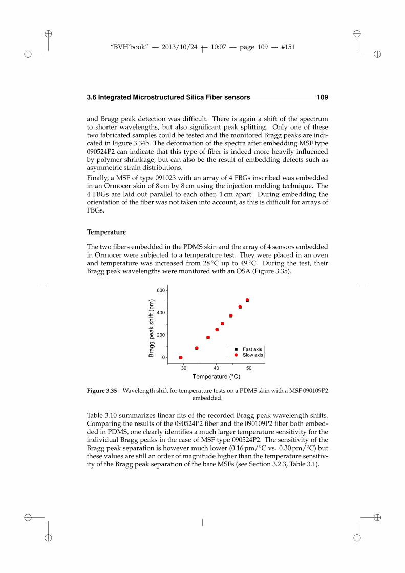
ii
“BVH˙book” — 2013/10/24 — 10:07 — page 109 — #151 ii
ii
ii
3.6 Integrated Microstructured Silica Fiber sensors 109
and Bragg peak detection was difficult. There is again a shift of the spectrumto shorter wavelengths, but also significant peak splitting. Only one of thesetwo fabricated samples could be tested and the monitored Bragg peaks are indi-cated in Figure 3.34b. The deformation of the spectra after embedding MSF type090524P2 can indicate that this type of fiber is indeed more heavily influencedby polymer shrinkage, but can also be the result of embedding defects such asasymmetric strain distributions.Finally, a MSF of type 091023 with an array of 4 FBGs inscribed was embeddedin an Ormocer skin of 8 cm by 8 cm using the injection molding technique. The4 FBGs are laid out parallel to each other, 1 cm apart. During embedding theorientation of the fiber was not taken into account, as this is difficult for arrays ofFBGs.
Temperature
The two fibers embedded in the PDMS skin and the array of 4 sensors embeddedin Ormocer were subjected to a temperature test. They were placed in an ovenand temperature was increased from 28 C up to 49 C. During the test, theirBragg peak wavelengths were monitored with an OSA (Figure 3.35).
Figure 3.35 – Wavelength shift for temperature tests on a PDMS skin with a MSF 090109P2embedded.
Table 3.10 summarizes linear fits of the recorded Bragg peak wavelength shifts.Comparing the results of the 090524P2 fiber and the 090109P2 fiber both embed-ded in PDMS, one clearly identifies a much larger temperature sensitivity for theindividual Bragg peaks in the case of MSF type 090524P2. The sensitivity of theBragg peak separation is however much lower (0.16 pm/C vs. 0.30 pm/C) butthese values are still an order of magnitude higher than the temperature sensitiv-ity of the Bragg peak separation of the bare MSFs (see Section 3.2.3, Table 3.1).

ii
“BVH˙book” — 2013/10/24 — 10:07 — page 110 — #152 ii
ii
ii
110 Integrated optical fiber sensors
Table 3.10 – Temperature sensitivities (pm/C) MSFs embedded in an PDMS or Ormocerskin. Standard error values (σ) reflect the variations between different experiments.
MSF type 090524P2 embedded in PDMS
fast axis slow axis peak separationpm/C linear fit σ linear fit σ linear fit σ
FBG1 47.09 1.86 47.25 1.80 0.16 0.07
MSF type 090109P2 embedded in PDMS
fast axis slow axis peak separationpm/C linear fit σ linear fit σ linear fit σ
FBG1 25.86 0.87 26.17 0.86 0.30 0.07
MSF type 091023K2 embedded in Ormocer (array of 4 FBGs)
fast axis slow axis peak separationpm/C linear fit σ linear fit σ linear fit σ
FBG1 7.83 0.43 8.22 0.51 0.38 0.10FBG2 7.65 0.55 8.26 0.58 0.61 0.06FBG3 7.48 0.68 8.07 0.68 0.59 0.07FBG4 8.35 0.48 8.53 0.51 0.18 0.06
A wavelength multiplexed array of FBGs inscribed in the MSF of type 091023Kand embedded in Ormocer has much lower temperature sensitivity of the indi-vidual Bragg peaks. This large difference between the two different host polymermaterials is due to the higher CTE of PDMS over Ormocer (see Section 3.3). Thetemperature sensitivity of the Bragg peak separation for this sample was againrather low ranging between 0.18 pm/C and 0.61 pm/C. The different sensitiv-ities monitored for the different FBGs inscribed in the same fibers are likely theresult of different orientations of the fiber sensors. A different orientation of thefiber will influence the effect of thermally induced stresses. These values for theBragg peak separation nevertheless confirm that the embedding process has aconsiderable impact on the temperature insensitivity of the sensor elements.
Contact pressure
The PDMS skin sample with two different types of fibers embedded is subjectedto different types of pressure tests. The skin is placed on a hard flat surface,while loads are applied at different positions. A pressure experiment was per-

ii
“BVH˙book” — 2013/10/24 — 10:07 — page 111 — #153 ii
ii
ii
3.6 Integrated Microstructured Silica Fiber sensors 111
formed with a load of 0.5 N that was applied with a metal ball with a diameterof 18 mm, as shown in Figure 3.36a. First, the shift of the individual Bragg peakswas monitored when the load was applied on several positions along a line thatcrosses the FBG sensor. The corresponding Bragg peak shifts for the FBG sensorfabricated in the MSF of type 090109P2 are shown in Figure 3.36b. A Gaussianfit was applied to the results and the details are summarized in Table 3.11. Themaximum peak shift for the mode polarized along the fast axis (33 pm) is 2 pmhigher than that of the mode polarized along the slow axis (31 pm). This impliesa very small change in Bragg peak separation when the load is directly placedon top of the FBG sensor. The same experiment was performed on the MSF oftype 090524P2 and the results are also summarized in Table 3.11. The maximumwavelength shift is larger for this sample, but no change in peak separation wasobserved. For both experiments, the Gaussian fits have a Full Width at Half Max-imum (FWHM) ranging between 1.4 mm and 1.5 mm. This is an indication for thedistance over which the embedded FBG sensor can still detect an applied load.
0,5 N
(a) Experimental set-up to apply a load tothe optical skin using a metal ball. (b) Individual Bragg peak shifts of a PDMS embedded
090109P2 MSF induced by the loading along a line thatcrosses the FBG.
Figure 3.36 – Contact pressure characterization of embedded MSFs.
Table 3.11 – Gaussian fits of the results of the Bragg peak shifts of PDMS embedded MSFs.
MSF type 090524P2 MSF type 090109P2
fast axis slow axis fast axis slow axisMax. peakshift (pm) 94 94 33 31
FWHM (mm) 1.44 1.54 1.41 1.44

ii
“BVH˙book” — 2013/10/24 — 10:07 — page 112 — #154 ii
ii
ii
112 Integrated optical fiber sensors
This experiment was extended to scan the sensitivity of the skin over a largerarea. Pressure was applied on more positions in an area of 6 mm x 13 mm, andfor each position the wavelength shifts were monitored. The result is shown inFigure 3.37. Although we again see an increased sensitivity of the individualBragg peaks at the position of the FBG, the influence of an applied load on theBragg peak separation is minimal.
Grating
position Grating
position
Grating
position
(a) Fast axis Bragg peak wavelength.
Grating
position Grating
position
Grating
position
(b) Slow axis Bragg peak wavelength.
Grating
position Grating
position
Grating
position
(c) Bragg peak wavelength separation.
Figure 3.37 – Contact pressure characterization of a PDMS skin with a 090109P2 MSF em-bedded. Color plots showing the wavelength change when a load of 0.5 N is applied at
different locations.
The same experiment was carried out but with the load increased up to 5 N. Al-though this higher pressure led to larger wavelength shifts, it also caused the

ii
“BVH˙book” — 2013/10/24 — 10:07 — page 113 — #155 ii
ii
ii
3.6 Integrated Microstructured Silica Fiber sensors 113
reflection spectra to deform when the skin was loaded directly or nearby the em-bedded FBG. When using a cylindrical load of 9 N and a larger flat contact surface(diameter 26 mm), these deformations did not take place. This is an indicationthat contact areas with dimensions comparable to that of the FBG (typically fewmm) can lead to spectrum deformations.Other experiments focused on the fibers embedded in Ormocer skins. First aload of 0.5 N was applied along a line on the skins that measures 1 cm by 4 cm.The experimental set-up was shown in Figure 3.36a. One of the contact pressureresults of an embedded MSF type 090109P2 sample is shown in Figure 3.38 andthe details of the Gaussian fits are listed in Table 3.12. For all three tested skinsa different maximum Bragg peak shift is observed for the modes polarized alongthe fast and the slow axis. This results in a shift in the Bragg peak separationwhen the load is applied on top of the FBG, albeit a small shift. The shift of theindividual Bragg peaks is again highest for the MSF of type 090524P2, as wasthe case for the PDMS skins. The FWHM of the Gaussian fits ranges between2 mm and 2.4 mm, indicating that sensors embedded in Ormocer skins can detectpressures over a larger area than sensors embedded in PDMS skins.
Figure 3.38 – Individual Bragg peak shifts of an Ormocer embedded 090109P2 MSF in-duced by the loading along a line that crosses the FBG.
Table 3.12 – Gaussian fits of the results of the Bragg peak shifts of Ormocer embeddedMSFs.
MSF type 090524P2 MSF type 090109P2Sample 1 Sample 1 Sample 2
fast axis slow axis fast axis slow axis fast axis slow axisMax. peakshift (pm) 120 117 74 66 50 37
FWHM (mm) 2.16 2.16 2.23 2.39 2.33 2.04

ii
“BVH˙book” — 2013/10/24 — 10:07 — page 114 — #156 ii
ii
ii
114 Integrated optical fiber sensors
The Ormocer skin with the array of FBGs embedded was tested with the sameexperimental set-up, but the load was increased to 5 N and a larger area wasscanned. For each position where a load was applied, the Bragg wavelengthsshifts were recorded and the results are shown in Figure 3.39. We see again anincreased sensitivity of both the individual Bragg peaks as the peak separationnearby the location of the FBG. However, the reflection spectra deformed heavilywhen the load was applied on top or close to the FBG. No reliable results wereconsequently obtained for these positions and they are therefore left blank in Fig-ure 3.39. It can be concluded that the practical applicability of the MSF sensors islimited using the polymer embedding technology in its current state.
FBG
2 mm
2 mm
2 mm
2 mm
FBG
(a)
FBG
2 mm
2 mm
2 mm
2 mm
FBG
(b)
Figure 3.39 – Contact pressure characterization of an Ormocer skin with a 091023 MSFembedded. Color plots showing the wavelength change when a load of 5 N is applied at
different positions.

ii
“BVH˙book” — 2013/10/24 — 10:07 — page 115 — #157 ii
ii
ii
3.6 Integrated Microstructured Silica Fiber sensors 115
3.6.2 Macrostructuring to enhance pressure sensitivity
In the previous section only small or moderate contact pressure sensitivities wereachieved for the Bragg peak separation of the MSFs embedded in either a PDMSor an Ormocer skin. In this paragraph, an approach is presented to overcomethe current limitations and increase the contact pressure sensitivity of the sensorelements via the use of macrostructuring.The experimental contact pressure skin results indicated that the transverse me-chanical sensitivity of the polymer embedded MSF system is significantly lowercompared to the bare MSF’s high transverse mechanical sensitivity. This is dueto the mismatch between the transducer layer (PDMS or Ormocer) and the silicafiber limiting the portion of stress transferred to the embedded Bragg grating. Tofully exploit the benefits of the microstructured fiber sensors, it is important to in-vestigate how physical quantities can be best transformed into a parameter thatcan be sensed locally by the fiber grating.To increase the compatibility between the embedding host material and the op-tical fiber, one possibility is to use the polymer optical fibers (Section 3.5). Asan alternative, it is possible to introduce a structure that maximizes the stressespresent in the region surrounding the optical fiber. This is investigated in de-tail within the PhD research of Sanne Sulejmani [13]. Figure 3.40 provides anoverview of a few macrostructuring possibilities and the theoretical increase ofthe peak separation pressure sensitivity.
Figure 3.40 – Overview of the possible improvement to the pressure sensitivity when dif-ferent types of macrostructures are applied.
Experimental work to fabricate these macrostructured grooves was performedby using a CO2 laser (λ=10.6 µm). Scanning different parameters (Figure 3.41)provided fabrication parameters for different groove widths and depths.First experimental results using macrostructuring grooves of almost 500 µm wide

ii
“BVH˙book” — 2013/10/24 — 10:07 — page 116 — #158 ii
ii
ii
116 Integrated optical fiber sensors
1.75 mm
180 μm
1.31 mm
420 μm
(a) Ablating 1 groove at0.8 mm/s
1.75 mm
180 μm
1.31 mm
420 μm
(b) Ablating 4 adjacent grooveswith 100 µm spacing at 2 mm/s
Figure 3.41 – Defining macrostructuring grooves by CO2 laser ablation using a pulse rep-etition frequency of 100 Hz, 0° attenuator, a circular mask with 4000 µm diameter and 10x
lens demagnification.
and 1.75 mm deep yielded a peak separation sensitivity of 55 pm/MPa. A samplewith a similar embedded MSF without grooves provided a reference sensitivityvalue of 25 pm/MPa.
3.7 Advanced fiber embedding
3.7.1 Locally embedded
Instead of full planar sensing layers, there is often a need for locally pressuresensitive islands. This way the application of an external strain or pressure is lo-calized on the fiber Bragg grating, enhancing the sensitivity of the fiber sensor,especially in the case of MSF, and avoiding cross-talk between the different sen-sor points.The interconnection between different sensing points is then based on(uncoated or coated) bare fiber. Using a dedicated mold, these pressure sensitiveislands can be fabricated. An example of such a mold is shown in Figure 3.42including fiber alignment tracks, material inlet and air outlet channels.Figure 3.43 is depicting an example of silica fiber Bragg gratings locally embed-ded in MED-6015, a PDMS material from Nusil [33] as well as a cross-sectionalview on the embedded silica fiber (with fiber coating, total diameter 250 µm).
3.7.2 Stacking optical skins
For respiratory monitoring applications, bend sensors are typically required. Oneoption is to mount two separate gratings symmetrically either side of the neutralaxis in an optical sensing skin. With such an arrangement, the difference between

ii
“BVH˙book” — 2013/10/24 — 10:07 — page 117 — #159 ii
ii
ii
3.7 Advanced fiber embedding 117
(a) Top view. (b) 6 pressure sensitive islands can be molded in parallel.
Figure 3.42 – Dedicated mold to fabricate locally embedded fiber Bragg grating sensors.
250 μm
900 μm
(a) Locally embedded sensor islands.
250 μm
900 μm
(b) Cross-sectional view- coated fiber.
Figure 3.43 – Silica fiber embedded in Nusil MED-6015 using dedicated mold.
the two Bragg wavelengths is sensitive to bending but not sensitive to commonmode strain or temperature. The stacking of two optical skins, each containinga single FBG, was achieved by plasma activating both optical skin surfaces, fol-lowed by an aligning and dry bonding step using an air plasma generator (DienerPico, 0.8 mbar, 24 s, 190 W, 40 kHz). Figure 3.44a depicts a schematic view onthis bonding process. Aligning the two optical skins before bringing them intocontact is done using a mask aligner system (SET MG1410) which was modi-fied by placing an adapter plate containing an extra vacuum chuck in the maskholder (holding Optical skin A in Figure 3.44b). Optical skin B was fixed in placeon the substrate table of the aligner, using another adapter plate and the stan-dard vacuum connection. Using the available positioning table and microscopeof the aligner system, it was possible to align both optical skins. Once aligned,the PDMS layers were brought into contact, creating an irreversible bond of theplasma treated layers.First prototypes of stacked silica and polymer fiber sensors are shown in Fig-ure 3.45. In the case of POFBG stacking, it is important to position the silica - POFglue joints sufficiently separated from each other.

ii
“BVH˙book” — 2013/10/24 — 10:07 — page 118 — #160 ii
ii
ii
118 Integrated optical fiber sensors
500 μm
Oxygen plasma treatment to active surfacelayers and improve bonding characteristics
Algining and bonding
Optical skin A
Optical skin B
(a) Schematic view.
Optical skin A
Optical skin B
Vacuum plate
Vacuum plate(b) Aligning two optical skins us-ing a modified mask aligner set-up.
Figure 3.44 – Stacking two optical skins through aligning and dry bonding through plasmasurface treatment.
Silica – POF glue joints
(a) POFBG.
Silica – POF glue joints
(b) Silica FBG.
Figure 3.45 – Stacking optical skins to perform bending/respiratory measurements.
3.8 Conclusion
Different fiber embedding techniques were developed in this chapter. Dependingon the application need, a soft or more stiff material can be chosen as a host ma-terial. Several embedding techniques were investigated: molding, laser ablationand soft-lithography, each possessing their specific advantages.The sensing elements used within this chapter are based on either Draw Tower
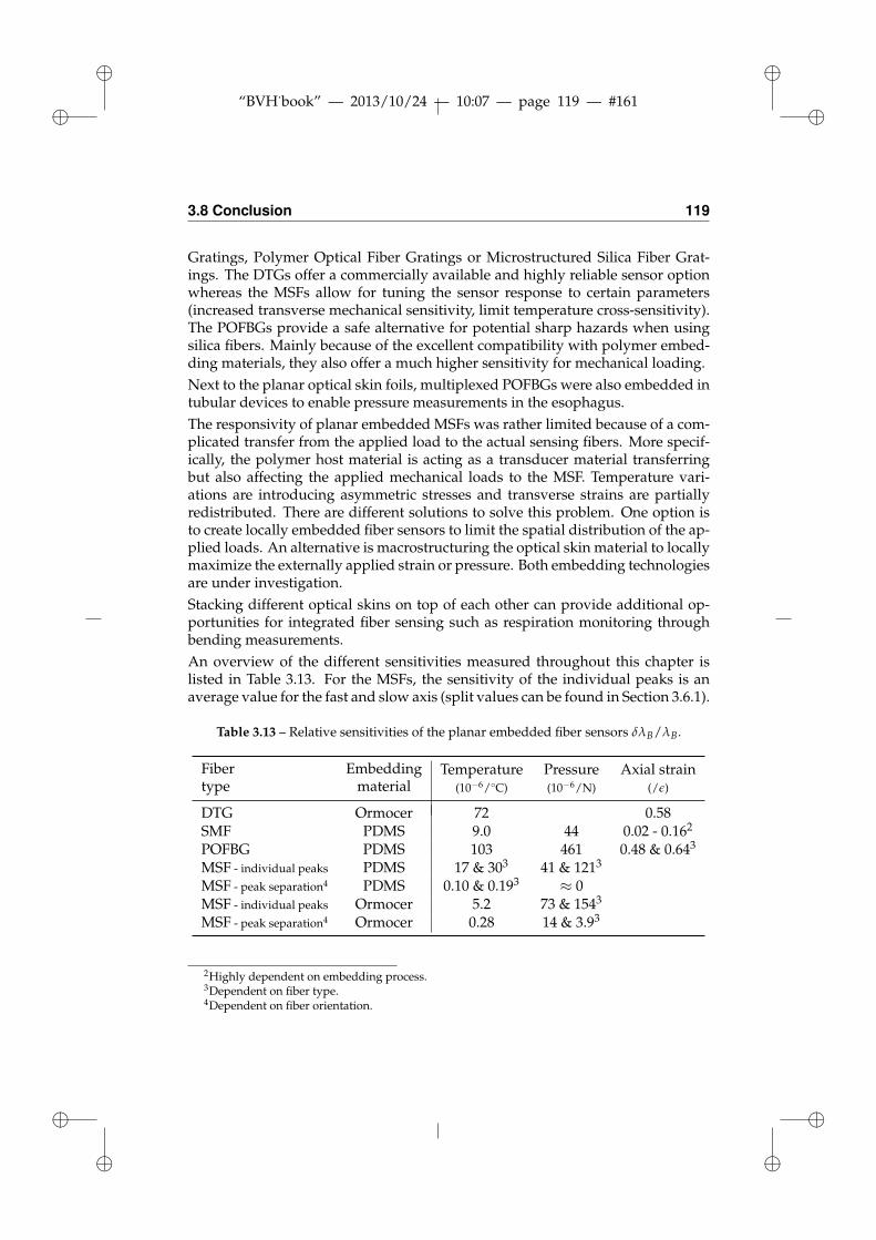
ii
“BVH˙book” — 2013/10/24 — 10:07 — page 119 — #161 ii
ii
ii
3.8 Conclusion 119
Gratings, Polymer Optical Fiber Gratings or Microstructured Silica Fiber Grat-ings. The DTGs offer a commercially available and highly reliable sensor optionwhereas the MSFs allow for tuning the sensor response to certain parameters(increased transverse mechanical sensitivity, limit temperature cross-sensitivity).The POFBGs provide a safe alternative for potential sharp hazards when usingsilica fibers. Mainly because of the excellent compatibility with polymer embed-ding materials, they also offer a much higher sensitivity for mechanical loading.Next to the planar optical skin foils, multiplexed POFBGs were also embedded intubular devices to enable pressure measurements in the esophagus.The responsivity of planar embedded MSFs was rather limited because of a com-plicated transfer from the applied load to the actual sensing fibers. More specif-ically, the polymer host material is acting as a transducer material transferringbut also affecting the applied mechanical loads to the MSF. Temperature vari-ations are introducing asymmetric stresses and transverse strains are partiallyredistributed. There are different solutions to solve this problem. One option isto create locally embedded fiber sensors to limit the spatial distribution of the ap-plied loads. An alternative is macrostructuring the optical skin material to locallymaximize the externally applied strain or pressure. Both embedding technologiesare under investigation.Stacking different optical skins on top of each other can provide additional op-portunities for integrated fiber sensing such as respiration monitoring throughbending measurements.An overview of the different sensitivities measured throughout this chapter islisted in Table 3.13. For the MSFs, the sensitivity of the individual peaks is anaverage value for the fast and slow axis (split values can be found in Section 3.6.1).
Table 3.13 – Relative sensitivities of the planar embedded fiber sensors δλB/λB.
Fibertype
Embeddingmaterial
Temperature(10−6/C)
Pressure(10−6/N)
Axial strain(/ε)
DTG Ormocer 72 0.58SMF PDMS 9.0 44 0.02 - 0.162
POFBG PDMS 103 461 0.48 & 0.643
MSF - individual peaks PDMS 17 & 303 41 & 1213
MSF - peak separation4 PDMS 0.10 & 0.193 ≈ 0MSF - individual peaks Ormocer 5.2 73 & 1543
MSF - peak separation4 Ormocer 0.28 14 & 3.93
2Highly dependent on embedding process.3Dependent on fiber type.4Dependent on fiber orientation.

ii
“BVH˙book” — 2013/10/24 — 10:07 — page 120 — #162 ii
ii
ii
120 Integrated optical fiber sensors
The aim of this chapter was to come up with a sensing skin based on polymerembedded fiber sensors. Depending on the application, a different embeddingapproach and fiber type can be selected. The tubular embedded polymer fibersensors proved to be compatible with esophageal measurement requirements.Embedded MSF sensors are typically used within harsh (high temperature andpressure) environments. Further research is needed however to maintain thefunctionality of these sensing systems once embedded in a polymer host mate-rial. Polymer optical fiber sensors have a relatively low reflectivity, limiting theoptions for fully embedded interrogation systems. For the remainder of this dis-sertation, the main focus is therefore on silica fiber sensors (DTG or other) inorder to come up with a proof-of-principle fiber sensing system. An outlook willbe provided towards specialty fiber sensors and polymer fiber sensors.

ii
“BVH˙book” — 2013/10/24 — 10:07 — page 121 — #163 ii
ii
ii
References 121
References
[1] A. Kersey, M. Davis, H. Patrick, M. LeBlanc, K. Koo, C. Askins, M. Put-nam, and E. Friebele, “Fiber grating sensors,” Journal of Lightwave Technology,vol. 15, no. 8, pp. 1442–1463, Aug. 1997.
[2] K. Hill and G. Meltz, “Fiber bragg grating technology fundamentals andoverview,” Journal of Lightwave Technology, vol. 15, no. 8, pp. 1263–1276, Aug.1997.
[3] FBGS International - DTG. (Accessed 2012) Draw tower grating®technology. [Online]. Available: http://www.fbgs.com/technology/dtg-technology
[4] FBGS International. (Accessed 2012) Company website. [Online]. Available:http://www.fbgs.com/
[5] E. Lindner, J. Moerbitz, C. Chojetzki, M. Becker, S. Brueckner, K. Schuster,M. Rothhardt, R. Willsch, and H. Bartelt, “Tailored draw tower fiber bragggratings for various sensing applications,” ser. Proceedings of SPIE, J. Can-ning and G. Peng, Eds., vol. 8351, 2012, 3rd Asia Pacific Optical SensorsConference (APOS), Sydney, Australia, JAN-FEB 2012.
[6] H. Dobb, D. Webb, K. Kalli, A. Argyros, M. Large, and M. van Eijkelenborg,“Continuous wave ultraviolet light-induced fiber bragg gratings in few- andsingle-mode microstructured polymer optical fibers,” Optics Letters, vol. 30,no. 24, pp. 3296–3298, Dec. 2005.
[7] I. P. Johnson, D. J. Webb, and K. Kalli, “Utilisation of thermal annealing torecord multiplexed fbg sensors in multimode microstructured polymer op-tical fibre,” ser. Proceedings of SPIE, W. Bock, J. Albert, and X. Bao, Eds., vol.7753, 2011, 21st International Conference on Optical Fiber Sensors, Ottawa,Canada, MAY 2011.
[8] P. S. J. Russell, “Photonic-crystal fibers,” Journal of Lightwave Technology,vol. 24, no. 12, pp. 4729–4749, Dec. 2006.
[9] T. Martynkien, G. Statkiewicz-Barabach, J. Olszewski, J. Wojcik, P. Mergo,T. Geernaert, C. Sonnenfeld, A. Anuszkiewicz, M. K. Szczurowski,K. Tarnowski, M. Makara, K. Skorupski, J. Klimek, K. Poturaj, W. Urbanczyk,T. Nasilowski, F. Berghmans, and H. Thienpont, “Highly birefringent mi-crostructured fibers with enhanced sensitivity to hydrostatic pressure,” Op-tics Express, vol. 18, no. 14, pp. 15 113–15 121, July 2010.
[10] M. Rothhardt, C. Chojetzki, and H. Mueller, “High mechanical strengthsingle-pulse draw tower gratings,” ser. Proceedings of the Society of Photo-Optical Instrumentation Engineers (SPIE), J. Armitage, R. Lessard, and
ii
“BVH˙book” — 2013/10/24 — 10:07 — page 122 — #164 ii
ii
ii
122 Integrated optical fiber sensors
G. Lampropoulos, Eds., vol. 5579, no. Part 1-2, 2004, pp. 127–135, in-ternational Conference on Applications of Photonics Technology, Ottawa,Canada, SEP 2004.
[11] T. Geernaert, M. Becker, P. Mergo, T. Nasilowski, J. Wojcik, W. Urbanczyk,M. Rothhardt, C. Chojetzki, H. Bartelt, H. Terryn, F. Berghmans, andH. Thienpont, “Bragg grating inscription in geo2-doped microstructured op-tical fibers,” Journal of Lightwave Technology, vol. 28, no. 10, pp. 1459–1467,May 2010.
[12] Phosfos Consortium. (2008) Photonic skins for optical sensing. [Online].Available: http://www.phosfos.eu/
[13] S. Sulejmani, Simulation, fabrication and characterization of bragg gratings in mi-crostructured fibers for sensing purposes. Master thesis, Vrije Universiteit Brus-sel, 2010.
[14] E. Ferraris, T. Van Gijseghem, C. Yan, B. Van Hoe, G. Van Steenberge,P. Van Daele, P. Dubruel, and D. Reynaerts, “Embedding of fibre optic sen-sors within flexible host,” in 4M/ICOMM 2009 - The Global Conference onMicro Manufacture, 2009, pp. 351–354, international Conference on Mult-Material Micro Manufacture/ International Conference on Micro Manufact-ing, Karlsruhe, Germany, SEP 2009.
[15] Dow Corning. (Accessed 2013) Company website. [Online]. Available:http://www.dowcorning.com/
[16] B. Ratner, Biomaterials science: an introduction to materials in medicine, ser. Aca-demic Press. Elsevier Academic Press, 2004.
[17] F. Bossuyt, T. Vervust, and J. Vanfleteren, “Stretchable electronics technol-ogy for large area applications: Fabrication and mechanical characteriza-tion,” IEEE Transactions on Components Packaging and Manufacturing Technol-ogy, vol. 3, no. 2, pp. 229–235, Feb. 2013.
[18] F. Schneider, T. Fellner, J. Wilde, and U. Wallrabe, “Mechanical properties ofsilicones for mems,” Journal of Micromechanics and Microengineering, vol. 18,no. 6, June 2008, 18th European Workshop on Micromechanics (MME 07),Univ Minho, Guimaraes, Portugal, SEP 2007.
[19] J. Missinne, “Development of conformable optical and optoelectronic basedtactile sensors,” Ph.D. dissertation, Ghent University, 2011.
[20] Micro resist technology GmbH. (Accessed 2013) Company website. [Online].Available: http://www.microresist.de/
[21] Ormocers. (Accessed 2013) Product website. [Online]. Available: http://www.ormocer.de/

ii
“BVH˙book” — 2013/10/24 — 10:07 — page 123 — #165 ii
ii
ii
References 123
[22] MicroChem. (Accessed 2013) Su-8 100 datasheet, available on companywebsite. [Online]. Available: http://microchem.com/
[23] B. Van Hoe, G. Van Steenberge, E. Bosman, J. Missinne, T. Geernaert,F. Berghmans, D. Webb, and P. Van Daele, “Optical fiber sensors embeddedin polymer flexible foils,” ser. Proceedings of SPIE-The International Societyfor Optical Engineering, F. Berghmans, A. Mignani, and C. Hoof, Eds., vol.7726, 2010, conference on Optical Sensing and Detection, Brussels, Belgium,APR 2010.
[24] S. Kiesel, K. Peters, T. Hassan, and M. Kowalsky, “Behaviour of intrinsicpolymer optical fibre sensor for large-strain applications,” Measurement Sci-ence & Technology, vol. 18, no. 10, pp. 3144–3154, Oct. 2007, 18th InternationalConference on Optical Fibre Sensors, Cancun, Mexico, OCT, 2006.
[25] N. Hawkes, “Laby, Th. - Tables of physical and chemical constants and somemathematical functions,” Nature, vol. 213, no. 5076, pp. 555–&, 1967.
[26] K. E. Carroll, C. Zhang, D. J. Webb, K. Kalli, A. Argyros, and M. C. J.Large, “Thermal response of bragg gratings in pmma microstructured op-tical fibers,” Optics Express, vol. 15, no. 14, pp. 8844–8850, July 2007.
[27] W. Zhang, D. J. Webb, and G. D. Peng, “Investigation into time response ofpolymer fiber bragg grating based humidity sensors,” Journal of LightwaveTechnology, vol. 30, no. 8, pp. 1090–1096, Apr. 2012.
[28] J. Barrie and B. Platt, “The diffusion and clustering of water vapour in poly-mers,” Polymer, vol. 4, no. 3, pp. 303–313, 1963.
[29] J. Lee, C. Park, and G. Whitesides, “Solvent compatibility ofpoly(dimethylsiloxane)-based microfluidic devices,” Analytical Chemistry,vol. 75, no. 23, pp. 6544–6554, Dec. 2003.
[30] G. Peng and P. Chu, “Polymer optical fiber photosensitivities and highlytunable fiber gratings,” Fiber and Integrated Optics, vol. 19, no. 4, pp. 277–293,2000.
[31] I. P. Johnson, K. Kalli, and D. J. Webb, “827 nm bragg grating sensor in mul-timode microstructured polymer optical fibre,” Electronics Letters, vol. 46,no. 17, pp. 1217–U74, Aug. 2010.
[32] C. Russell, N. Bright, G. Buthpitiya, L. Alexander, C. Walton, and G. Whe-lan, “Esophageal propulsive force and its relation to manometric pressure,”GUT, vol. 33, no. 6, pp. 727–732, June 1992.
[33] Nusil Silicone Technology. (Accessed 2013) Company website. [Online].Available: http://www.nusil.com/

ii
“BVH˙book” — 2013/10/24 — 10:07 — page 124 — #166 ii
ii
ii

ii
“BVH˙book” — 2013/10/24 — 10:07 — page 125 — #167 ii
ii
ii
4Integrated optoelectronic components
for optical sensors
Optoelectronic components are needed to drive, read out and interpret the optical sensorsand the according sensing information. Within this chapter, a technology is developedto embed these necessary driving and read-out elements for optical sensors in ultra-thinoptoelectronic packages based on polymer materials. A thorough selection of suitable op-toelectronic components is performed, studying both the compatibility with the opticalsensing elements and the possibility to embed these components using polymer basedintegrated packages. Although this embedding technology is providing a generic opto-electronic packaging process, the intended application is the integrated interrogation ofoptical fiber sensors. The selection of the appropriate components is therefore based onthis criterion.
4.1 Introduction
When using sensors based on optical working principles, the optomechanicalproperties of the sensing medium are changing when certain environmental pa-rameters are adjusted (as was discussed in Chapter 2). To read out and visualizethese changes, a light source and mostly also a detector are needed. Dependingon the sensing and interrogation principle (extensively discussed in Chapter 2,Sections 2.1 and 2.2), the type of source and detector can seriously differ.

ii
“BVH˙book” — 2013/10/24 — 10:07 — page 126 — #168 ii
ii
ii
126 Integrated optoelectronic components for optical sensors
For all sensing systems within this dissertation, a major objective is an exten-sive integration through embedding and miniaturization of the sensors and theaccording interrogation systems. In this chapter, the necessary technology is de-veloped to address this objective in terms of the optoelectronics. Depending onthe sensor type, additional dedicated technology blocks may be required. In thecase of fiber sensing systems, separate technology building blocks are necessaryfor the fibers (Chapter 3) and the coupling of the fibers and the optoelectronics(Chapter 5). Sensors based on a working principle inherent in the optoelectroniccomponents, such as the shear sensor discussed in Section 2.1.1 or the pressuresensor discussed in Section 2.1.2, are not involving any light guiding structures.They can consequently rely on only the optoelectronics integration technology.When fabricating traditional optoelectronic semiconductor active chip packages,one typically has to chose between several technology options. These technologychoices are related to the interconnection technology, such as face up placement(wire bonding) or flip chip (solder bumps, ball grid arrays), and the packagingtechnology, such as Dual In-Line (DIL) or Multi-Chip Modules (MCM). The re-sulting packages are mounted on a carrier substrate such as a rigid Printed Cir-cuit Board (PCB) or a flexible substrate. The thickness and size of such modulescan be a limiting factor when using these chip packages for example in wear-able systems, for biomedical purposes (such as minimally invasive surgery) orwithin structural health monitoring applications. In this chapter, a technologyis described to come up with an ultra-thin, unobtrusive and mechanically flex-ible optoelectronic package. Light emitting III-V components and detectors aretherefore integrated in a spin-coated polymer stack consisting of epoxy and/orpolyimide materials.The integration challenges strongly depend on the component type (metalization,light emitting area, heatsinking etc.). A selection of the most promising opticalsources and detectors is consequently imposed. As we will see later on, there areseveral trade-offs to be considered in this context including for example sensorinterrogation speed versus interrogation accuracy and multiplexing possibilitiesversus system cost.
4.1.1 Ultra-thin packaging
By making the driving elements and associated peripheral materials as thin andsmall as possible, it is possible to come up with an unobtrusive alternative for thetraditional PCB technology which is typically combined with surface-mounteddevices. The optoelectronic components are therefore manipulated on a bare dielevel. Bare dies are typically used in high-end systems where conventional pack-aging might result in unacceptable levels of degradation in electrical, mechanicalor thermal performance [1]. In this chapter, the optoelectronic bare die compo-nents are thinned down and embedded in an ultra-thin optical package. This chip

ii
“BVH˙book” — 2013/10/24 — 10:07 — page 127 — #169 ii
ii
ii
4.2 Selection of optoelectronic components 127
level integration enables a high degree of mechanical flexibility and formability.
4.1.2 Polymer embedding
Using polymers as embedding host material and consequently avoiding the tra-ditional PCB laminates is further limiting the dimensions of the total chip pack-age. The main driver behind the use of materials from the polymer family ishowever the possibility to make non-toxic, human-friendly or potentially evenbiocompatible applications.
4.1.3 Wavelength selection
This chapter has to enable the combination of the optoelectronics with opticalfibers and fiber sensors. Fiber Bragg gratings typically have reflecting wave-lengths in the range of 850 nm or 1550 nm. The main advantage of the 1550 nmcomponents is the compatibility with off-the-shelf telecom equipment (sources,fibers, detectors). In terms of cost, the 850 nm devices provide a good alternativebecause of the possibility to work with Silicon (Si) or Gallium Arsenide (GaAs)devices. At a wavelength of 850 nm, optical losses in polymer based fibers orwaveguides are also significantly lower than at 1550 nm. When selecting the ap-propriate wavelength, one has to take into account these different pros and cons.
4.2 Selection of optoelectronic components
The necessary optoelectronics for optical fiber sensors have to meet certain re-quirements:
• Availability of the component in an unpackaged - bare die - version.
• Wavelength compatibility with the fiber Bragg grating wavelengths.
• Minimum level of in-fiber optical power budget.
• Modal behavior allowing for an unambiguous fiber sensor read-out.
Within this PhD research and related projects (Chapter 1, Section 1.8), severaltypes of unpackaged semiconductor optoelectronic sources were obtained as baredies, both in the 850 nm and 1550 nm wavelength range. An overview of theoptoelectronic components (bare die) available for further integration is providedin Table 4.1. The price/die values mentioned in this table are only indicative.All components were then investigated to check their suitability for use with fibersensors. To perform this comparison, they were not yet integrated in a polymerpackage but rather mounted as bare die on a rigid carrier.

ii
“BVH˙book” — 2013/10/24 — 10:07 — page 128 — #170 ii
ii
ii
128 Integrated optoelectronic components for optical sensors
Table 4.1 – Overview of the available (bare die) optoelectronic sources.
edge-emitting top-emittingLD SLED LED VCSEL VCSEL VCSEL
Company Roithner Exalos Roithner BeamExpress ULMPhotonics
ULMPhotonics
Reference [2] [3] [2] [4] [5] [5]Price/die e 10 e 250 e 2 e 50 e 11 e 6
λcentral 1550 nm 850 nm1550 nm 1550 nm 1550 nm 850 nm 850 nm
Modes SM/MM SM MM SM SM MM
Poptical, total 6 mW 10.5 mW20 mW 2.5-5 mW 1.2 mW 2.5 mW 1.5 mW
Bandwidth 3-5 nm 50 nm65 nm 130 nm 0.15 nm 0.1 nm 0.3 nm
4.2.1 LED
A Light Emitting Diode (LED) is a very low-cost optoelectronic source candi-date offering a broad spectral output range. A 1550 nm surface emitting unpack-aged LED (ELC-1550-17) from Roithner [2] was mounted on a substrate and wirebonded to copper tracks. A 3D translation stage was used to position a barefiber end of a 50 µm core multimode pigtail close to the LED in order to maxi-mize coupling. The remote end of the pigtail was connected to either an OSA orpower meter. The optical power measured in the fiber is very low, never reaching1 µW. Furthermore there is a non-linear relationship between power and currentat higher drive currents, possibly because of the device overheating due to lack ofheatsinking. The spectral width is very wide (FWHM of 145 nm) but this widthin combination with the very low power in-fiber means that the power reflectedfrom any sensing grating would be insufficient for any practical application. Thereflected power needed would of course depend on the specific application andits associated signal-to-noise requirements, but is always likely to be above a fewµW which is already greater than the optical power this source would provide.The low in-fiber power is due to the fact that the LED emission angle is very large.

ii
“BVH˙book” — 2013/10/24 — 10:07 — page 129 — #171 ii
ii
ii
4.2 Selection of optoelectronic components 129
Figure 4.1a shows the far field beam profile of the LED, measured with a beamprofiler (Photon Inc. goniometric radiometer, available at B-Phot, VUB).
4.2.2 LD
An edge-emitting unpackaged Laser Diode (LD, chip 1550-5) from Roithner [2]was mounted and monitored in a similar fashion to the LED. The power vs. cur-rent curve displays typical laser behavior with a well defined threshold current(at I = 12 mA). Power in the multimode fiber is over a mW, and this coupled withthe narrow spectral profile would lead to a good signal-to-noise ratio when inter-rogating a grating. Figure 4.1b shows the measured beam profile of the Roithnerlaser diode. As expected, the coupling of the laser diode light beam is much moreefficient than for the LED. There is however a pronounced modal structure visi-ble in the beam profile. This is more problematic since during interrogation of agrating the peaks in the modal structure of the source can essentially be mistakenfor the peak in the grating reflectivity.
(a) Roithner LED. (b) Roithner laser diode.
Figure 4.1 – Measured beam profiles using a goniometric radiometer.
4.2.3 SLED
An edge-emitting unpackaged Superluminescent Light Emitting Diode (SLED,EXS1510) from Exalos [3] was mounted and monitored in a similar fashion to theLED and LD. The optical output that we expect from this component is in therange of 5 mW-20 mW, while the actual measured optical power is in the rangeof µWs. The reason for this can be found in the thermal heating of the chip. Noactive cooling is present with the given mounting set-up, only passive heatsinkcooling. The driver current range of the SLED is up to 300 mA, which is con-siderably higher compared to the other components (typical driving currents of

ii
“BVH˙book” — 2013/10/24 — 10:07 — page 130 — #172 ii
ii
ii
130 Integrated optoelectronic components for optical sensors
about 1 mA-20 mA). This is causing the bad optical behavior of the wire bondedcomponent, driven with a continuous electrical current.In cooperation with the SLED provider (Exalos [3]), this effect was investigatedin more detail. Analyzing the SLED behavior resulted in the observation of athermal roll-over causing a spectral collapse with strong red shifting (up to 60 nm,Figure 4.2b) near the ASE threshold (driving current of 150 mA, Figure 4.2a). Wehave however shown the possibility to drive the components with a modulateddriving current to lower the duty cycle and avoid the thermal overheating effects.The resulting optical power coupled to a fiber increases in this case to 3 mW.The optical power values are still significantly lower than expected and normalspectral behavior is shifted to lower driving currents, still indicating a higher chiptemperature. To guarantee continuous wave operation and/or full power pulsedoperation of the SLED and avoid thermal problems, the thermal mass has to beincreased and the thermal resistance of the n-contact has to be reduced. This canbe done for example by using thicker copper traces or heat pipes in combinationwith multi-layer heat-spreading PCBs. These solutions are evidently severelylimiting the integration possibilities of this component.
4.2.4 VCSEL
An unpackaged Vertical-Cavity Surface-Emitting Laser (VCSEL, 1550 nm) fromBeamExpress [4] was mounted and monitored in a similar fashion to the LEDand LD. The VCSEL displays a well defined threshold current of 1.9 mA. Thepower available in-fiber is good (Figure 4.3a shows the measured beam profile ofthe BeamExpress 1550 nm VCSEL to confirm the excellent coupling opportuni-ties) and later experiments with higher currents and better adjustment achievedin-fiber power over 1 mW. The beam profile shows an average beam divergenceof 8.15° (FWHM). Equally good is the source spectrum, which consists of a singleemission peak of less than 0.2 nm width. Electrothermal tuning of the BeamEx-press VCSEL central wavelength, necessary to drive a fiber sensor, is possible toa limited extent (Figure 4.3b). Depending on the fiber type and the application(transducer material, parameter range), a wavelength range of 1 nm up to a fewnm is needed to interrogate a single fiber Bragg grating sensor. The wavelengthresolution of commercially available (OSA or peak tracking) systems is typicallyranging from a few 10 pm down to 1 pm.Depending on the fiber sensor wavelength, also 850 nm VCSEL components areused. The characteristics of these components are similar to the 1550 nm devicesand are not shown here. Detailed beam profile analysis of these components willbe discussed in view of fiber coupling possibilities within Chapter 5.Only the VCSELs and SLEDs are consequently retained for the remainder of thischapter.

ii
“BVH˙book” — 2013/10/24 — 10:07 — page 131 — #173 ii
ii
ii
4.2 Selection of optoelectronic components 131
1.2
1.4
1.6
0.10
0.12
0.14
Ou
tpu
t P
ow
er
[mW
]
Ex‐facet cw SLED.V
0.0
0.2
0.4
0.6
0.8
1.0
0.00
0.02
0.04
0.06
0.08
0 50 100 150 200 250 300 350
Vo
ltag
e [
V]
Ou
tpu
t P
ow
er
[mW
]
Bias Current [mA]
(a) Low optical output power and thermal roll-over near ASE threshold.
‐50
‐45
‐40
320 300 280 260 240 220
200 180 160 140 120 100
‐70
‐65
‐60
‐55
‐50
1520 1540 1560 1580 1600 1620 1640 1660 1680 1700
Wavelength [nm]
Drivingcurrent[mA]
Spe
ctra
l den
sity
[dB
m /
0.1n
m]
Increasing driving current
(b) Spectral collapse with strong red shifting starting at 150 mAindicating a huge thermal problem.
Figure 4.2 – Continuous wave characterization of a 1550 nm wire bonded SLED, per-formed at Exalos.

ii
“BVH˙book” — 2013/10/24 — 10:07 — page 132 — #174 ii
ii
ii
132 Integrated optoelectronic components for optical sensors
(a) Measured beam profile using a goniometricradiometer.
1550 15521551 1553 1554 1555Wavelength [nm]
2 mA
3 mA
4 mA5 mA
-50
-40
-20
-30
-10
0
Pow
er [
dB]
(b) Modal structure and electrothermaltuning effects.
Figure 4.3 – 1550 nm wire bonded VCSEL characterization.
4.3 Chip thinning and back contacting
Typical chip thicknesses of the available optoelectronic components range be-tween 100 µm and 150 µm. Aiming for an ultra-thin optoelectronic package basedon thin-film processing steps, the individual optoelectronic chips are thinneddown to 20 µm. Thinning down optoelectronic components typically consistsof several lapping and polishing steps. This thinning procedure was previouslyoptimized for several types of (opto)electronic components, such as microcon-trollers (PhD Wim Christiaens [6], Chapter 6), multimode 850 nm VCSEL arraysand GaAs photodetector arrays (PhD Erwin Bosman [7], Chapter 5).Within this dissertation also active optoelectronic components at 1550 nm areused. The substrate material is in this case not Si or GaAs but mostly IndiumPhosphide (InP), an even more brittle material. Therefore the thinning technol-ogy was thoroughly investigated for InP substrates. An additional challenge onthinning down the different available components is the fact that some compo-nents have a top and a bottom contact. Because the thinning process physicallyremoves a large part of the chip backside bulk material, the back-contact metal-ization layer is completely removed after this thinning process. These two chal-lenges are now discussed in more detail. Table 4.2 gives an overview of the sub-strate materials and contact structures of the different investigated optoelectron-ics.
4.3.1 Thinning InP substrates
The technology to thin down GaAs VCSELs and Photodiodes (PDs) was taken asa starting point to introduce the thinning of InP substrates (SLEDs/VCSELs). All

ii
“BVH˙book” — 2013/10/24 — 10:07 — page 133 — #175 ii
ii
ii
4.3 Chip thinning and back contacting 133
Table 4.2 – Overview of the contact and bulk information of the different investigatedoptoelectronics.
Component Substrate material Electrical contacts
1550 nm single-mode SLED InP Top-Bottom1550 nm single-mode VCSEL InP Top-Top850 nm single-mode VCSEL GaAs Top-Bottom850 nm multimode VCSEL GaAs Top-Top
lapping and polishing work of optoelectronic chips is consequently performed onthe Logitech PM5 Precision Lapping & Polishing Machine installed in the CMSTcleanrooms. InP in general is even more fragile than GaAs, which is translatedto a more delicate thinning process. The technology to thin down InP substrateswas developed using dummy substrates. In order to prepare dummy InP chips,a sample (1 cm x 1 cm) from an InP wafer (thickness 500 µm) was thinned downto 125 µm and was cleaved into smaller pieces, matching the dimensions of theSLEDs (1500 µm x 500 µm). The dummy components were mounted onto thetemporary rigid glass carrier with wax for further lapping and polishing to a finalthickness of 30 µm. Fine-tuning of the different process parameters was required:
• The wax for fixation of the dies to the temporary carrier: glycophtalate.
• A minimal load on the dies with support of large InP dummy samples.
• The lapping step is done using a suspension of 3 µm Al2O3 grains on aglass lapping plate. This results in a fast removal rate (4 min to thin the diefrom 125 µm to 40 µm) with low surface damage after lapping using a platerotation speed of 10 rpm.
• The polishing step consists of mechanical polishing with very fine 0.3 µmAl2O3 on a soft cloth resulting in a low edge roundness and low surfaceroughness. The polishing process is much slower and takes about 20 min tothin the dies further from 40 µm to 30 µm. Again a plate rotation speed of10 rpm is used.
Figure 4.4 shows the roughness of the backside of an InP die after lapping andpolishing measured with a non-contact optical profilometer (WYKO) indicatingan average roughness less than 3 nm on a 120 µm x 92 µm surface. The technologyis ready-to-use on functional devices.

ii
“BVH˙book” — 2013/10/24 — 10:07 — page 134 — #176 ii
ii
ii
134 Integrated optoelectronic components for optical sensors
um
um
1200 10 20 30 40 50 60 70 80 90 100 110
92
0
10
20
30
40
50
60
70
80
-133
109
50
0
-50
-100
nm
TFCG Microsystems
Rz:V 159.55Vnm
Ra:V 2.93VnmRq:V 4.68Vnm
Title:VNote:V
Date:V 26/03/2009
Time:V 23:58:13
Mag:V 51.3VX
Mode:V VSI
Surface Statistics:
Surface Data
Size:V736VXV480
Set-up Parameters:
Sampling:V 163.74Vnm
Processed Options:
CylinderVyVTiltV
None
Filtering:
TermsVRemoved:
Rt:V 242.39Vnm
Figure 4.4 – An optical profiler scan (WYKO NT3300) of the InP substrate after lappingand polishing.
4.3.2 Applying a back-contact layer
In order to enable the application of a new back-contact layer, an additionalsmaller carrier substrate is used during the lapping and polishing process (Fig-ure 4.5). The reason for this is twofold: firstly, the application of a back-contactwill be done using sputtering and Chemical Vapor Deposition (CVD) in a vac-uum chamber with limited dimensions requiring a small carrier. Secondly, thebig carrier substrate associated with the Logitech PM5 Precision Lapping & Pol-ishing Machine can easily be reused as no metalization or annealing steps areapplied on this substrate.After releasing the small carrier (Carrier 2) from the mother carrier (Carrier 1), anew back-contact metalization layer AuGeNiAu stack is deposited by evaporat-ing (AuGe and Au) and sputtering (Ni) consecutively 150 nm AuGe, 60 nm Niand 200 nm Au. When releasing the chips from the wax, the complete metal-ization layer will be attached to the chip. To enable the release of the individu-ally mounted components, the thin metal layer is therefore first removed aroundthe chip using laser ablation. More specifically, a 355 nm Nd:YAG laser (86 mW,10 kHz, dynamic: 1 mm/s) is used to remove the AuGeNiAu stack on a patharound the optoelectronic chip. Dissolving the mounting wax in acetone releasesthe individual chips with a typical thickness of 20-30 µm. As a final step, a ther-mal annealing step (fast alloy up to 440° in 10 % H2-N2 forming gas environment)is applied to produce an ohmic contact.

ii
“BVH˙book” — 2013/10/24 — 10:07 — page 135 — #177 ii
ii
ii
4.3 Chip thinning and back contacting 135
This process was developed to apply back-contact layers to thinned individualchips and is in its current state not suitable for large quantities of optoelectroniccomponents. It nevertheless provides a way to thin, embed and test back con-tacted chips within the CMST cleanrooms.
Carrier 1 Carrier 2 Dummy 1
Dummy 2
SLED/VCSEL
Figure 4.5 – Introducing an extra carrier (Carrier 2) which is released from Carrier 1 afterlapping and polishing.
4.3.3 Thinning of functional devices
The different types of functional components listed in Table 4.2 are now thinneddown to a thickness of a few 10 µm. This mechanical thinning process based onindividual die thinning is applied for the first time on SLEDs, 1550 nm VCSELsand 850 nm single-mode VCSELs.
850 nm ULM Photonics multimode VCSELs
Thinning multimode 850 nm VCSELs from ULM Photonics was optimized andextensively discussed within the PhD of Erwin Bosman [7] and is therefore notrepeated here. This thinning process formed the basis for the thinning technologydeveloped within this chapter. The material substrate is GaAs and all contactpads are situated on the top surface of the chip.
1550 nm BeamExpress VCSELs
The 1550 nm BeamExpress VCSELs were thinned down to 40 µm thickness (orig-inal thickness is 125 µm). Figure 4.6a shows a picture of the thin VCSEL andFigure 4.6b shows the measured VI curve of the chip after gluing the thinnedcomponent to a substrate and wire bonding the contacts to contact lines on thesubstrate. The measured characteristics are the same as for the unthinned com-ponents (reference graph included in Figure 4.6b).

ii
“BVH˙book” — 2013/10/24 — 10:07 — page 136 — #178 ii
ii
ii
136 Integrated optoelectronic components for optical sensors
(a) Stereozoom picture. 0 0.5 1 1.5 2 2.50
2
4
6
8
10
12
14
16
I [m
A]
V [V]
chip thickness: 125 µmchip thickness: 40 µm
(b) Electrical characterization.
Figure 4.6 – Characterization of the 1550 nm BeamExpress VCSEL.
1550 nm Exalos SLEDs
SLEDs are much larger components (1500 µm x 500 µm) than the VCSELs (350 µmx 250 µm for the 1550 nm VCSELs). Together with the fact that InP is the most brit-tle material, we can say that the thinning process for the SLED is the most delicate.Applying the thinning process to these SLEDs however results in good backsidesurface quality and no chip damage. Figure 4.7 shows pictures of the backside ofan SLED after lapping (a), after polishing (b) and after backside metalization (c).Figure 4.8a shows pictures of the SLED top surface after thinning and metaliza-tion (40 µm thick). The VI curves of the SLED in unthinned and in thinned statusare compared in Figure 4.8b. A small deviation in the curves is observed. The im-pact of this deviation in the optical output of the SLED could not be measured atthis moment since the DC-driving of the component results in unusual behaviorof the chip due to overheating by the lack of active cooling. Modulated driving ofthe chip, using a limited current duty cycle (10 % at 100 kHz), has proven to solvethis problem, but is not implemented in this section.
850 nm ULM Photonics single-mode VCSELs
A WYKO 3D profile of the top surface of a thinned and back contacted 850 nmsingle-mode VCSEL is shown in Figure 4.9. This optical profilometer plot showsthat the gold bump surrounding the active area is about 8 µm (reference plane= top surface of chip). This resulted in an extra challenge for the thinning andembedding process. When the components are wax-mounted on the temporaryglass carrier before the thinning procedure, a weight is put on the dies to uni-

ii
“BVH˙book” — 2013/10/24 — 10:07 — page 137 — #179 ii
ii
ii
4.3 Chip thinning and back contacting 137
(a) After lapping. (b) After polishing.
(c) After back contacting, before laser cuttingand release.
Figure 4.7 – Thinning and back contacting single-mode 1550 nm Exalos SLEDs.
(a) Picture of the top surface after thin-ning and metalization (40 µm thick).
0 0.5 1 1.5 20
50
100
150
200
250
300
350
I [m
A]
V [V]
chip thickness: 125 µmchip thickness: 40 µm
(b) Electrical behavior before and after chip thin-ning.
Figure 4.8 – Characterization of the 1550 nm SLED.

ii
“BVH˙book” — 2013/10/24 — 10:07 — page 138 — #180 ii
ii
ii
138 Integrated optoelectronic components for optical sensors
10.0
21.4
20.0
19.0
18.0
17.0
16.0
15.0
14.0
13.0
12.0
11.0
10.0
um
Date: 08/27/2010Time: 15:44:17
Title: SubregionNote: X offset:178 Y offset:83
3-Dimensional Interactive Display
Ra: 7.16 um
Rq: 8.18 um
Rt: 25.72 um
Magnification: 10.49
Measurement Mode: VSISampling: 801.09 nm
Array Size: 369 X 317
Surface Stats:
Measurement Info:
Date:-08/27/2010
Time:-15:44:17
Title:-SubregionNote:-X-offset:178- Y-offset:83
3-Dimensional-Interactive-Display
Ra:I7.16Ium
Rq:I8.18Ium
Rt:I25.72Ium
Magnification:I10.49
MeasurementIMode:IVSI
Sampling:I801.09Inm
ArrayISize:I369IXI317
Surface-Stats:
Measurement-Info:
20
18
16
14
12
10
21.4
μm
Figure 4.9 – WYKO non-contact optical profilometer plot of a single-mode 850 nm VCSEL.
formly spread out the wax layer underneath the chip. The protruding gold bumparound the active area will however carry most of the weight. When the slightesthorizontal shift of the dies in the molten wax occurs, the gold bump will be de-formed and spread out over the active area. Figure 4.10a shows an extreme caseof this deformation, resulting in a completely covered active area of the VCSEL.This problem was solved by dropping down the weight on top of the dies in avery controlled way to avoid any horizontal movement of the weight during thelowering of the weight. No deformation of the gold bump was observed sincethen.After lapping and thinning of the dies, they are kept inside the wax layer on thetemporary glass carrier and the back-contact metalization is applied. The waxprotects the sides of the chip to be metalized and avoids the creation of a short tothe top active layers of the chip. Figure 4.10b shows a picture of the laser cut back-contact layer before release of the chips. After release of the chip by removing thewax with acetone, it is glued on a copper substrate with electrical conductingglue and wire bonded to copper tracks on the same substrate. The measured VIand LI curves of the original non-thinned and thinned devices are included inthe graphs in Figure 4.11. The curves are almost identical which guarantees asuccessful back contacting after the thinning process.
4.3.4 Conclusion
The thinning and back contacting technology for OE components is available.We will now turn our focus towards the embedding of the thinned optoelec-

ii
“BVH˙book” — 2013/10/24 — 10:07 — page 139 — #181 ii
ii
ii
4.3 Chip thinning and back contacting 139
(a) Picture of a clearly deformed goldbump around the active area, covering the
complete active area.
(b) Picture of the laser cut metal layer before releasingthe chip.
Figure 4.10 – Thinning, back contacting and releasing single-mode VCSEL chips.
0 0.5 1 1.5 20
0.25
0.5
0.75
1
1.25
1.5
1.75
2
I [m
A]
V [V]
chip thickness: 150 µmchip thickness: 25 µm
(a) Electrical characterization.
0 0.5 1 1.50
0.1
0.2
0.3
0.4
0.5
0.6
Opt
ical
Wpow
erW
IW[mA]
chipWthickness:W150WµmchipWthickness:W25Wµm
[mW
]
(b) Optical characterization.
Figure 4.11 – Characterization of an unthinned vs. a thinned (thickness of 25 µm) 850 nmsingle-mode ULM Photonics VCSEL.

ii
“BVH˙book” — 2013/10/24 — 10:07 — page 140 — #182 ii
ii
ii
140 Integrated optoelectronic components for optical sensors
tronic dies in polymer packages. Because of higher driving currents and limitedheatsink possibilities, the SLEDs are challenging to integrate. The developmentof the integration technology is therefore focused on a VCSEL - top-emitting -approach. As an example, we take a single-mode 850 nm VCSEL from ULM Pho-tonics and a photodetector from Albis. Two approaches have been investigatedand are discussed in detail in the following sections.
4.4 SU-8 based flat optoelectronic package
Two types of packages have been investigated: the first type is based on an epoxyembedding material, SU-8, a negative photoresist from MicroChem [8]. The sec-ond type is based on a polyimide embedding material, PI-2611 from HD Mi-crosystems [9]. Each process flow has its specific advantages and shortcomings.The main advantage of the first approach is the possibility to work with a singlechip embedding layer matching the thickness of the chip. This results in a flat op-toelectronic package providing an easy fiber coupling interface for optoelectroniccomponents with vertically oriented active areas (VCSEL, PD). Also other impor-tant advantages are associated with this approach. They include for example thepossibility to reliably stack different chip packages on top of each other (outsidethe scope of this dissertation).
4.4.1 Process flow
Embedding optoelectronic components in ultra-thin flexible packages was firstinvestigated within the PhD dissertation of Erwin Bosman. The end result wasan SU-8 based package enabling integrated flexible optical datacom links. Thisprocess flow ([7], Chapter 6, Sections 6.2 and 6.4) was used as a starting point andoptimized from an optical sensing point of view to enable the embedding of (backcontacted) single-mode optoelectronic components and facilitate fiber coupling(minimize the optical path length). The detailed process flow is schematicallyshown in Figure 4.12. As a result, an optoelectronic component is embedded inan ultra-thin polymer package. When bending and manipulating this ultra-thinpackage, the highest stresses in the polymer optoelectronic stack can be found inthe outer layers. By applying layers of polyimide on both sides of the stack asphysical supporting layers, we can spread the high stress inside the outer poly-mer layer over a larger area than just the manipulated area. Polyimide has a highstrength and flexibility which makes it the ideal support material.The fabrication of the ultra-thin optical chip package starts on a rigid temporaryglass carrier on which a thin (8 µm thickness) and mechanically strong polyimidelayer (PI-2525, HD Microsystems [9]) is spin-coated. Since there is no adhesionof this layer with the glass carrier, it can easily be released after completing the

ii
“BVH˙book” — 2013/10/24 — 10:07 — page 141 — #183 ii
ii
ii
4.4 SU-8 based flat optoelectronic package 141
(a) Applying a polyimide and
patterning a Cu ground layer
(b) Applying a SU-8 layer and
defining a cavity by laser ablation
(c) Placing the thinned chip in
the cavity using a glue
(d) Leveling the chip in the cavity
(e) Covering with SU-8 and laser
ablating vias to the chip contacts
(f) Metalizing the top contacts
(Cu patterning)
(g) Applying a covering SU-8
and polyimide layer
(h) Releasing the ultra thin
optical package
Figure 4.12 – Schematic overview of the SU-8 based flat optoelectronic package processflow.
fabrication. To ensure sufficient adhesion during the process, an adhesion pro-moter (Pyralin VM652) is applied on the edges of the glass carrier. A 1 µm copperheatsink layer, which can also function as a back contacting layer, is sputtered ontop of the PI layer and, if needed, electro-plated up to the desired copper thick-ness. Next, this metal layer is structured using a wet etch CuCl2 process (a). AnSU-8 embedding layer is spin-coated on top and, using a 10.6 µm CO2 and 248 nmKrF Excimer laser, a chip embedding cavity is ablated (b) to mount (c), level (d)and fix an optoelectronic chip. The thickness of this SU-8 layer is approximatingthe thickness of the chip increased with ≈ 5 µm (thickness of glue layer under-neath the chip). Depending on the contact pad structure, a thermally conductiveglue (U 8449-9, Namics Corporation) or an Isotropic (thermally and electrically)Conductive Adhesive (ICA), CE3103 WLV from Emerson & Cuming is used.

ii
“BVH˙book” — 2013/10/24 — 10:07 — page 142 — #184 ii
ii
ii
142 Integrated optoelectronic components for optical sensors
The result of the chip leveling is measured using a non-contact optical profilome-ter. Measuring 10 embedded single-mode VCSELs, an average of 0.77° with astandard deviation of 0.57° is obtained after leveling and after glue curing.A thin (few µm) SU-8 covering layer is applied on top of the chip and microviasare drilled using an Excimer laser to access the chip contact pads (e). A top con-tacting 1 µm Cu layer is sputtered and structured (f) and again a thin polymerSU-8 layer is spin-coated on top to protect the metal contact pads (g). The fi-nal processing layer consists of applying a thin polyimide layer identical to thestarting polyimide layer. To make contact with the outside world, the polymerscovering the chip contact fan-out pads are locally removed using laser ablation(CO2 and KrF Excimer). The flexible optoelectronic package with a total thick-ness of 40 µm is now ready for release (h). To the best of our knowledge, suchPI/SU-8 ultra-thin flexible optoelectronic packages including single-mode andback contacted laser chips are reported for the first time.This generally described embedding process can be used to embed several typesof optoelectronic components including VCSELs and PDs. As mentioned before,the optical out-coupling facet quality is guaranteed in the case of vertically emit-ting or accepting components (surface quality of top surface is defined by thefinal spin-coating step). When combining this integration process with edge-emitting components however, one should provide an optical facet on the sideof the package (surface quality of side surface is defined by the release method)with a roughness which is low enough for coupling purposes. In the remainderof this section, this process flow is applied on single-mode VCSELs at 850 nm andGaAs photodetectors for fiber sensing purposes. Figure 4.13 is depicting a fewexamples of single-mode VCSELs integrated in a PI/SU-8 package.
Bottom
contacts
Top contacts
Embedded single mode 850 nm VCSEL
Figure 4.13 – Single-mode 850 nm VCSELs embedded in a PI/SU-8 package.
The embedded single-mode VCSELs are now characterized in detail, both elec-trically and optically, in order to check their functionality and compatibility withfiber sensing applications. Next to the preservation of single-mode behavior af-

ii
“BVH˙book” — 2013/10/24 — 10:07 — page 143 — #185 ii
ii
ii
4.4 SU-8 based flat optoelectronic package 143
ter chip thinning, polishing and embedding, efficient and optical skin compliant(i.e. compatible with planar sensing layers) fiber coupling of the VCSELs is alsoan important prerequisite for the envisaged application. This will be tackled in adedicated chapter (Chapter 5).
4.4.2 Characterization
In this section, we investigate the influence of three important parameters on theelectrical and optical characteristics of the SU-8 embedded single-mode VCSELs:
• Substrate material. Processing the ultra-thin polymer stack on a rigid PCB(FR4) board is compared with the polyimide supported flexible package,processed on a glass carrier.
• Chip thickness. The thickness of the chip is varied and the influence isstudied (“chip: xx µm” is referring to the embedded chip thickness).
• Heatsink layer thickness. An important parameter for the thermal resis-tance of the optoelectronic package are the dimensions of the heatsink layerbeneath the chip. The thickness of this layer is varied (“Cu: xx µm” is refer-ring to the heatsink layer thickness).
0 0.5 1 1.5 2 2.5 3 3.50
1
2
3
4
5
Cur
rent
[mA
]
Voltage [V]
unthinned chipCu: 17 µm, chip: 45 µmCu: 17 µm, chip: 25 µmCu: 1 µm, chip: 25 µm
Figure 4.14 – Electrical characterization of SU-8 embedded optoelectronic single-modeVCSELs on a rigid FR4 substrate with varying Cu heatsink thickness and chip thickness.

ii
“BVH˙book” — 2013/10/24 — 10:07 — page 144 — #186 ii
ii
ii
144 Integrated optoelectronic components for optical sensors
The electrical characterization results for the PCB substrates are depicted in Fig-ure 4.14. The results are typically averaged over two packages. These curvescorrespond nicely with the data in Figure 4.11a from the original (not-embedded,unthinned) components. The deviation in the “Cu: 1 µm, chip: 25 µm” case isprobably due to the fact that there was only 1 package measured for this case.The electrical characterization results for the PI on glass substrates are depictedin Figure 4.15 again showing averaged values. These curves correspond nicelywith the data in Figure 4.11a from the original (not-embedded, unthinned) com-ponents.
0 0.5 1 1.5 2 2.5 3 3.50
1
2
3
4
5
Cur
rent
[mA
]
Voltage [V]
unthinned chipCu: 1 µm, chip: 45 µmCu: 10 µm, chip: 25 µmCu: 1 µm, chip: 25 µm
Figure 4.15 – Electrical characterization of SU-8 embedded optoelectronic single-modeVCSELs on a PI ground layer with varying Cu heatsink thickness and chip thickness.
The optical characterization results for the PCB substrates are depicted in Fig-ure 4.16 again showing averaged values. These curves are in line with the datain Figure 4.11b from the original (not-embedded, unthinned) components. Thedifference in absolute optical power values is probably due to the inherent chip-to-chip variation. Bare chip LI slope efficiencies are varying between 0.3 W/Aand 0.7 W/A according to the datasheet. Also the alignment of the Newport 818series optical power detector used for these measurements can have an influenceon the absolute power values. A saturation effect can however be noticed in allpackage types indicating potential thermal problems when using high DC driv-ing currents.The optical characterization results for the PI on glass substrates are depicted inFigure 4.17 again showing averaged values.

ii
“BVH˙book” — 2013/10/24 — 10:07 — page 145 — #187 ii
ii
ii
4.4 SU-8 based flat optoelectronic package 145
0 1 2 3 40
0.5
1
1.5
2O
ptic
al p
ower
[mW
]
Current [mA]
unthinned chipCu: 17 µm, chip: 45 µmCu: 17 µm, chip: 25 µmCu: 1 µm, chip: 25 µm
Figure 4.16 – Optical characterization of SU-8 embedded optoelectronic single-modeVCSELs on a rigid FR4 substrate with varying Cu heatsink thickness and chip thickness.
0 1 2 3 40
0.5
1
1.5
2
Opt
ical
pow
er [m
W]
Current [mA]
unthinned chipCu: 1 µm, chip: 45 µmCu: 10 µm, chip: 25 µmCu: 1 µm, chip: 25 µm
Figure 4.17 – Optical characterization of SU-8 embedded optoelectronic single-modeVCSELs on a PI ground layer with varying Cu heatsink thickness and chip thickness.

ii
“BVH˙book” — 2013/10/24 — 10:07 — page 146 — #188 ii
ii
ii
146 Integrated optoelectronic components for optical sensors
These curves are again in line with the data in Figure 4.11b from the original (not-embedded, unthinned) components. The difference in absolute optical powervalues is also probably due to the inherent chip-to-chip variation. A saturationeffect can nevertheless again be noticed in all package types indicating potentialthermal problems when using high DC driving currents.Besides the LI (optical power versus electrical driving current) characteristics,also the electrothermal wavelength tunability will be an important propertywhen using the VCSELs in combination with fiber sensors. This effect is alsomeasured (DC driving) and shown in Figure 4.18 for the PCB substrates andFigure 4.19 for the PI on glass substrates. A more detailed discussion, includingdynamic measurements, is included in Chapter 6, Section 6.6.
1 2 3 4
855
856
857
858
859
Wav
elen
gth
[nm
]
Current [mA]
Cu: 17 µm, chip: 45 µmCu: 17 µm, chip: 25 µm Cu: 1 µm, chip: 25 µm
Figure 4.18 – Wavelength tuning of SU-8 embedded optoelectronic single-mode VCSELson a rigid FR4 substrate with varying Cu heatsink thickness and chip thickness.
An overview graph depicting the differences in wavelength tunability (nm/mA),both in terms of substrate, chip thickness and heatsink thickness, is shown inFigure 4.20. The wavelength tuning effect is largely based on an electrothermalheating of the chip imposing a difficult trade-off between optimal heat dissipa-tion and maximum wavelength tuning. The thin PI based package provides amore efficient heat dissipation compared to the FR4 substrate resulting in lowerwavelength tuning ranges. Tuning ranges are significantly higher for reducedchip thickness and heatsink thickness values indicating an increased electrother-mal effect and higher peak temperatures. There is consequently an additionaltrade-off between a minimized total thickness of the chip package leading to a

ii
“BVH˙book” — 2013/10/24 — 10:07 — page 147 — #189 ii
ii
ii
4.4 SU-8 based flat optoelectronic package 147
higher degree of mechanical flexibility combined with higher wavelength tuningranges, and an optimal heat management build-up.
1 2 3 4
855
856
857
858
859
Wav
elen
gth
[nm
]
Current [mA]
Cu: 1 µm, chip: 45 µmCu: 10 µm, chip: 25 µm Cu: 1 µm, chip: 25 µm
Figure 4.19 – Wavelength tuning of SU-8 embedded optoelectronic single-mode VCSELson a PI ground layer with varying Cu heatsink thickness and chip thickness.
0.7
0.74
0.78
0.82
0.86
FR4 PI 25 μm 45 μm
Wav
elen
gth
tu
nab
ilit
y [
nm
/mA
]
Substrate Chip thickness Heat sink thickness
10-17 μm 1 μm
Figure 4.20 – Wavelength tuning of SU-8 embedded optoelectronic single-mode VCSELs.Average values depending of substrate, chip thickness and heatsink thickness.

ii
“BVH˙book” — 2013/10/24 — 10:07 — page 148 — #190 ii
ii
ii
148 Integrated optoelectronic components for optical sensors
4.5 PI based low-stress optoelectronic package
Because of the difference in the Coefficient of Thermal Expansion (CTE, listedin Table 4.3), the PI-2525/SU-8 based ultra-thin polymer stack can suffer from aconsiderable amount of mechanical stress. This can be an issue when a releasedpackage is used for fiber coupling and further embedding. The alternative whichis presented here is based on a single polyimide embedding material (PI-2611, HDMicrosystems [9]) with a CTE close to the semiconductor materials resulting ina low-stress optoelectronic package. A potential drawback is the non-flatness ofthe polymer stack introducing different step coverages, for example of the opto-electronic chip. Another challenge is the higher curing temperature (> 300 C) ofthe PI-2611 vs. the PI-2525/SU-8 embedding stack. The OE components consid-ered in this chapter prove to be compatible with the proposed embedding flowand according process temperatures but this is not guaranteed when changingthe type of component. This process flow is strongly inspired by the work of RikVerplancke ([10], Chapter 4). Within his PhD, a stretchable electronics platformusing thin dies, using different polymers including PI-2611, was developed.
Table 4.3 – Overview of the coefficients of thermal expansion of different semiconductor(left) and polymer embedding (right) materials.
Material CTE (ppm/C)
Si 3InP 4.5GaAs 6
Material CTE (ppm/C)
PI-2611 3PI-2525 40SU-8 52
4.5.1 Process flow
Figure 4.21 shows a schematic overview of the fabrication of this low-stress opto-electronic package. Processing for this type of package again starts on a rigid tem-porary glass carrier with selectively applied adhesion promoter (Pyralin VM652)on which a polyimide (PI-2611, HD Microsystems) is spin-coated (6 µm thick-ness). A 1 µm copper layer is sputtered on top. Heatsinks which can simulta-neously act as bottom contact layers are patterned using a wet etching (CuCl2)process (a). The dimensions of the copper heatsinks are 4.5 mm x 4.5 mm, pro-viding sufficient heat spreading capabilities with only a limited influence on themechanical flexibility. Next, a PI-2611 layer (6 µm thickness) is spin-coated ontop and a chip embedding cavity is ablated (b) using a 248 nm KrF Excimer lasercombined with the parameters listed in Table 4.4. Then, an ultra-thin (20 µm)chip is placed (c), leveled and fixed (d) in the cavity using a thermally conduc-tive glue (U 8449-9, Namics Corporation) or an ICA (thermally and electrically

ii
“BVH˙book” — 2013/10/24 — 10:07 — page 149 — #191 ii
ii
ii
4.5 PI based low-stress optoelectronic package 149
conductive), CE3103 WLV from Emerson & Cuming Isotropic. Leveling of thechips is again measured using a non-contact optical profilometer. Measuring 25embedded components, an average of 0.46° with a standard deviation of 0.22° isobtained after leveling before glue curing and an average of 0.57° with a stan-dard deviation of 0.31° is found after thermal curing of the adhesive. The op-toelectronic chip is subsequently covered by spin-coating a PI-2611 layer (6 µmthickness) and microvias (diameter 40 µm) are drilled (e) using a 248 nm KrF Ex-cimer laser (200 mJ/cm2, 100 Hz, static: 50-70 pulses/location) to reach the chiptop contacts. Top metalization is performed by sputtering and patterning a 1 µmCu layer (f). This copper layer is protected by a top covering PI-2611 layer (6 µmthickness), again applied by spin-coating (g). To make contact with the outsideworld, the polymer layers covering the chip contact fan-out pads are locally re-moved using laser ablation (CO2 and KrF Excimer). The optoelectronic packagewith a total thickness of 40 µm is then ready for release (h). To the best of ourknowledge, such PI based ultra-thin flexible optoelectronic packages includ-ing single-mode and back contacted laser chips are reported for the first time.
Table 4.4 – Chip embedding cavity in PI-2611: laser ablation parameters.
Parameter Value
Laser Excimer, λ = 248 nmProjection mask 2000 µm x 2000 µmSpot size 200 µm x 200 µmPulse energy 80 µJPulse repetition frequency 100 HzFluence 200 mJ/cm2
Dynamic: stage translation speed 1 mm/sStatic: # pulses 20 pulses/location
Before each polyimide spin-coating step (except for the starting PI layer), theunderlying PI surface is slightly roughened after hard bake by exposing it for1 min to an oxygen (O2) plasma. A System VII Batchtop RIE (Plasma-Therm) wasused for this purpose with following parameters: RF power 150 W, O2 flow rate25 sccm and chamber pressure 150 mTorr. This Reactive Ion Etching (RIE) step isperformed to improve the adhesion with the covering layer.Resulting PI-2525/SU-8 packages with embedded photodetector arrays (4 activeareas) are shown in Figure 4.22. Figure 4.22b includes a special fan-out copperdesign which will ease the alignment of the fiber coupling plug (Chapter 5).
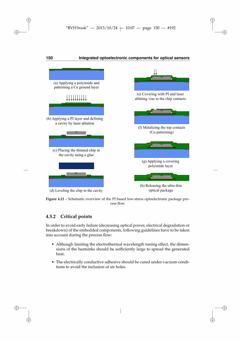
ii
“BVH˙book” — 2013/10/24 — 10:07 — page 150 — #192 ii
ii
ii
150 Integrated optoelectronic components for optical sensors
(a) Applying a polyimide andpatterning a Cu ground layer
(b) Applying a PI layer and defininga cavity by laser ablation
(c) Placing the thinned chip inthe cavity using a glue
(d) Leveling the chip in the cavity
(e) Covering with PI and laserablating vias to the chip contacts
(f) Metalizing the top contacts(Cu patterning)
(g) Applying a coveringpolyimide layer
(h) Releasing the ultra thinoptical package
Figure 4.21 – Schematic overview of the PI based low-stress optoelectronic package pro-cess flow.
4.5.2 Critical points
In order to avoid early failure (decreasing optical power, electrical degradation orbreakdown) of the embedded components, following guidelines have to be takeninto account during the process flow:
• Although limiting the electrothermal wavelength tuning effect, the dimen-sions of the heatsinks should be sufficiently large to spread the generatedheat.
• The electrically conductive adhesive should be cured under vacuum condi-tions to avoid the inclusion of air holes.

ii
“BVH˙book” — 2013/10/24 — 10:07 — page 151 — #193 ii
ii
ii
4.5 PI based low-stress optoelectronic package 151
Contact pads openedby laser ablation
Photodetectorchip
(a) Releasing a PI-2611 embedded pho-todetector after opening contact pads.
(b) Released photodetector package with dedi-cated “butterfly” contact fan-out design.
Figure 4.22 – Result of the PI-2611 embedding process flow.
• The sample should be exposed to the highest processing temperature, typi-cally during glue curing, before applying the chip covering layer.
4.5.3 Characterization
The electrical and optical characterization results are similar to the SU-8 basedprocess flow results and are therefore not repeated in this section.In Figure 4.23, a cross-sectional investigation of a PI-2611 embedded single-modeVCSEL is shown. Figure 4.23a is showing the areas which are investigated inmore detail in Figures 4.23b-4.23e. A good step coverage of the different layersstacked on the optoelectronic chip can be observed. The electrical top contactinginterface does not show any delamination. In the Scanning Electron Microscope(SEM) images however, one can observe a few potential inclusions of air holes inthe electrically conductive adhesive layer.Figure 4.24 is showing an embedded chip with a thickness of only 10 µm. Becauseof increasing mechanical stresses, the chip itself starts to bend hindering a properlayer build-up of the polymer package.
4.5.4 Reliability
Thinning and embedding unpackaged (opto)electronic chips in ultra-thin pack-ages with a guaranteed performance level is a huge challenge. The well estab-lished traditional packages and according reliability standards do not apply andespecially the combination with polymers can be an issue. Moisture can slowlypenetrate the system, causing oxidation of galvanic interconnects and swellingof polymer material, resulting in stresses and - in the end - defects. The best

ii
“BVH˙book” — 2013/10/24 — 10:07 — page 152 — #194 ii
ii
ii
152 Integrated optoelectronic components for optical sensors
Figure (e)
Figure (b) – (d)
(a) Overview microscope image.
42 μm
3.1 μm 3.5 μm
20 μm
6.6 μm
(b) Edge of the chip and PI/Cu step coverage(back illumination).
42 μm
3.1 μm 3.5 μm
20 μm
6.6 μm
(c) Edge of the chip and PI/Cu stepcoverage (dark field image).
(d) SEM image - potentialair hole inclusion.
(e) SEM image - detailed view on microviaand top metalization.
Figure 4.23 – Cross-section of a PI-2611 embedded VCSEL.
Figure (e)
Figure (b) – (d)
10 μm
30 μm
Figure 4.24 – 30 µm chip package with an embedded 10 µm VCSEL.

ii
“BVH˙book” — 2013/10/24 — 10:07 — page 153 — #195 ii
ii
ii
4.5 PI based low-stress optoelectronic package 153
way to estimate the life time of a system is to put it through accelerated agingtests. Therefore, initial reliability 85/85 (temperature-humidity) tests have beenperformed on 10 single-mode 850 nm VCSELs embedded in a PI-2611 stack. Thesamples were stored for 1000 h in a climate chamber under controlled temper-ature and humidity conditions. The selected temperature/humidity profile con-sisted of the well-known 85 C/85 % RH parameters. Each time before measuringthe electrical and optical characteristics, the environmental conditions are gradu-ally changed to 30 C/30 % RH for 30 min.The results are shown in Figure 4.25. During the first 500 hour, the electrical DCimpedance (VVCSEL/IVCSEL @ IVCSEL = 6 mA) and optical power is monitoredeach 50 h. Between 500 h and 1000 h, the measurement interval is changed to100 h. After 500 h, the packages are consequently exposed for the first time toan uninterrupted period of 100 h at 85° and 85 % RH. This can explain the unex-pected drop of optical power (extra loss of 0.36 dB) at t = 600 h. Another observa-tion is the gradual increase of the electrical impedance, which is less pronouncedtowards the end of the reliability measurements. All optical and electrical mea-surements are however within a 10 % range indicating that the effect of acceler-ated aging might be limited.
0 200 400 600 800 1000
−0.4
−0.3
−0.2
−0.1
0
0.1
Ave
rage
9opt
ical
9loss
9[dB
]
Time9[hours]0 200 400 600 800 1000
0.36
0.37
0.38
0.39A
vera
ge9D
C9r
esis
tanc
e9[kΩ
]
Optical9powerElectrical9impedance
0.4
Figure 4.25 – 85/85 reliability test performed on embedded 850 nm single-mode VCSELsmonitoring both electrical and optical properties. All measurements are performed using
a DC driving VCSEL current, IVCSEL = 6 mA.

ii
“BVH˙book” — 2013/10/24 — 10:07 — page 154 — #196 ii
ii
ii
154 Integrated optoelectronic components for optical sensors
4.6 Conclusion
Within this chapter, a polymer integration technology is developed to integratelaser and detector chips within polymer packages. The electrical interconnectionis provided through sputtered thin-film copper layers. As a polymer embeddinglayer, different spin-on polyimide and epoxy materials are used. To limit thethickness of the total chip package, individual optoelectronic chips are thinneddown to 20 µm and, if necessary, back-contacts are reapplied and alloyed. Theresult is an ultra-thin optoelectronic chip package incorporating single- or multi-mode sources or detectors in the 850 nm or 1550 nm wavelength range. This me-chanically flexible optoelectronic package has a typical thickness of only 40 µm.Furthermore, the packaging approach based on a PI-2525/SU-8 or PI-2611 em-bedding stack was shown to have a limited influence on the operation of thedevices.From an embedding point of view, the GaAs 850 nm components are preferredover the InP 1550 nm components, because of a more robust substrate material interms of handling and thinning. In terms of cost, beam divergence, optical powergeneration and electrical power consumption, the VCSEL components turned outto be the ideal candidates as a driving source for the fiber sensing systems.Applying this integration technology using SM VCSELs and PDs on fiber sensingapplications, the interrogation system will be based on the electrothermal red-shift observed in the VCSEL wavelength when varying the driving current. Atypical wavelength range of 3 nm can be covered using the embedded VCSELs.This is offering only limited possibilities to exploit the multiplexing features ofoptical fiber sensors, but provides a cost-effective and highly accurate way toread out the optical sensors. Moreover, using this ultra-thin integration tech-nology enables the fabrication of fully embedded interrogation systems with anunprecedented degree of miniaturization.A fiber sensing system based on the integrated optoelectronic components as wellas a detailed discussion on the interrogation principles is included in Chapter 6.But before doing so, the final technology chapter is describing the coupling of theintegrated optoelectronic components and optical fiber(s) (sensors).

ii
“BVH˙book” — 2013/10/24 — 10:07 — page 155 — #197 ii
ii
ii
References 155
References
[1] Universal Enterprise - leading distributor of semiconductor bare die, waferand packaging in China/Asia. (Accessed 2013) Company website. [Online].Available: http://www.ue.com.hk/
[2] Roithner LaserTechnik. (Accessed 2013) Products. [Online]. Available:http://www.roithner-laser.com/
[3] EXALOS: Superluminescent Light Emitting Diodes (SLEDs) Manufacturer.(Accessed 2013) Products. [Online]. Available: http://www.exalos.com/
[4] BeamExpress. (Accessed 2012) Products. [Online]. Available: http://www.beamexpress.com/
[5] Ulm-Photonics. (Accessed 2012) Products. [Online]. Available: http://www.ulm-photonics.com/
[6] W. Christiaens, “Active and passive component integration in polyimide in-terconnection substrates,” Ph.D. dissertation, Ghent University, 2009.
[7] E. Bosman, “Integration of optical interconnections and opto-electronic com-ponents in flexible substrates,” Ph.D. dissertation, Ghent University, 2010.
[8] MicroChem - Innovative Chemical Solutions for MEMS and Mi-croelectronics. (Accessed 2013) Company website. [Online]. Available:http://microchem.com/
[9] HD MicroSystems, an enterprise of Hitachi Chemical and DuPont.(Accessed 2013) Company website. [Online]. Available: http://hdmicrosystems.com/
[10] R. Verplancke, “Generic technology platform for the integration of micro-electronics and microfluidics on stretchable substrates,” Ph.D. dissertation,Ghent University, 2013.

ii
“BVH˙book” — 2013/10/24 — 10:07 — page 156 — #198 ii
ii
ii

ii
“BVH˙book” — 2013/10/24 — 10:07 — page 157 — #199 ii
ii
ii
5Coupling integrated optoelectronic
components
The embedding technology and the characterization of embedded fiber sensors and opto-electronics have been described extensively in previous chapters. To combine several ofthese building blocks into a functional sensing system, a dedicated coupling technologyis needed to integrate the optoelectronic driving and read-out units combined with thesensor structures. This technology should provide a low-loss, robust, small, skin compat-ible (i.e. enabling embedding in thin planar sensing skins), low-cost solution for couplingsingle and multimode optoelectronic sources to optical waveguiding (typically fiber sens-ing) structures. A generic compact coupling technology accommodating these needs isdeveloped within this chapter.
5.1 Introduction
Laser diode packages can generally be divided in three categories: butterfly, TO-can (coaxial) and dual in-line. The common configuration for laser diode trans-mitters in optical communications is the butterfly configuration. Most of the costof these modules is due to the process of packaging, which includes the couplingof the laser diode to an optical (single-mode or multimode) fiber via certain opti-cal coupling schemes and the firm attachment of all components at their optimumpositions inside the module [1].

ii
“BVH˙book” — 2013/10/24 — 10:07 — page 158 — #200 ii
ii
ii
158 Coupling integrated optoelectronic components
A rather outdated but still very relevant statistic [2] shows that the commercialmarket for optical telecommunication components had reached $5 billion in 2001.And more importantly, about 60 % to 80 % of the manufacturing cost of thesecomponents comprises fiber pigtailing and packaging (see Figure 5.1). A majorportion of the packaging cost is associated with active alignment and attachmentof chip-to-chip and single-mode fibers to chips. Active alignment involves light-ing up input fibers and active components and maximizing light throughput be-fore attachment. It is clear that the coupling scheme and resulting fiber pigtailingtechnology are of major importance and have to be chosen judiciously.
Presented at Optoelectronics Packaging and MOEMS Topical Workshop, IMAPS, Bethlehem, PA 2002
Figure 1. Packaging as a fraction of total manufacture cost of an optical modulator. 2.0 Introduction to LIGA The LIGA process was developed in Germany at the Institute fo r Nuclear Engineering (IMT)). LIGA is an acronym for the main steps of the process, i.e., deep X-ray lithography, electroforming, and pl astic molding. Thes e three steps make it possible to mass-produce micro-components with sub-micron features and large aspect ratios at a low-cost. We will only give a brief description here since the process is well documented in the liter ature (Becker, 1986; Lorenz et al., 1997; C hang and Kim, 2000). Figure 2 shows the main steps in the LIGA process schematically. Deep X-ray lithography allows structures of any lateral design with high aspect ratios to be produced, i.e., with heights of up to 3 m m and a la teral resolution down t o 0.2 µm. The walls of these struct ures are smooth and parallel to each other . The ver y sophisticated structures of this type can be pr oduced lithographically only by the highly penetrating, intense, and parallel X-rays suppl ied by a synchrotron. The structural information is compiled by means of a CAD system and then stored on a mask meeting the special requirements of har d X-radiation. Synchrotron r adiation is used to transfer the lateral structural information into a pl astics layer, normally polymethylmethacrylate (PMMA), by "shadowing." Expos ure to radiation (step 1) modifies the plastic material in
0
1000
2000
3000
4000
5000
6000
1998 1999 2000 2001
Year
Dev
ice
Cos
t ($)
Chip CostPackaging Cost
Figure 5.1 – Packaging as a fraction of the total manufacture cost of an optical modulatorduring the millennium transition.
Within this chapter, a generic compact fiber coupling technology is developed.The specific application which is driving this technology is an optical fiber sens-ing system, fabricated as flat and small as possible enabling embedding in thinoptical skins. The coupling technology will therefore be used to deliver inte-grated and skin-compliant fiber-coupled optoelectronic components. Like theembedding host material, the material used in the coupling scheme is preferablya (biocompatible) polymer. The coupling scheme itself is based on existing con-figurations using V-groove technologies, micro-mirrors and intermediate wave-guides but combined to yield a fiber-coupled ultra-thin package. This chapterincludes design, modeling and fabrication of the coupling technology, as well asevaluation of the alignment accuracy.Throughout this chapter, several technology choices have to be made to nar-row down the options both in terms of the optoelectronic components and thecoupling technology. Starting from the conclusions of Chapter 4, only SLEDsand VCSELs are withheld as optoelectronic driving sources in Section 5.2. In Sec-tion 5.3, a VCSEL is selected as the final optoelectronic source and initial couplingsimulations prove a direct coupling approach to be more efficient compared to anintegrated intermediate waveguide approach. Finally, in Sections 5.4-5.6, a ded-icated planar coupling technology for single-mode VCSELs is developed. The

ii
“BVH˙book” — 2013/10/24 — 10:07 — page 159 — #201 ii
ii
ii
5.2 Optoelectronic component selection 159
structure of this chapter is schematically shown in Figure 5.2.
OE component selection
Coupling technology
SLED or VCSEL
VCSEL Single-mode VCSEL
Direct butt coupling
skin compatible 45° micromirror
5.2 5.3 5.4 5.5 5.6 Section
1st gen. 2nd gen.
Figure 5.2 – Technology choices within Chapter 5.
The optical simulations (Lumerical and ASAP) performed within this chapterwere defined in close collaboration with and carried out by B-Phot, VUB withinthe framework of the European project Phosfos [3]. It is also important to men-tion that, although the coupling medium is different (waveguides versus fibers),the coupling concepts and associated technologies are strongly inspired by thework of dr. Erwin Bosman. Within his PhD dissertation [4] (Chapter 7, and morespecifically Sections 7.4.2 and 7.5), a polyimide based 90° optical mirror insertfor flexible polymer optical interconnects was developed based on a dedicated45° clamping tool to lap and polish mirror facets. For the final (VCSEL-fiber-PD)coupling schemes in this dissertation, a similar clamping tool is used albeit withdifferent materials and processing steps.
5.2 Optoelectronic component selection
Before fiber pigtailing, the optoelectronic components are packaged by em-bedding them in ultra-thin optical packages. Several types of semiconductorlasers were looked into, both in the 850 nm and 1550 nm wavelength range. Anoverview of the optoelectronic components (bare die), available for embeddingand coupling, is again provided and combined with the conclusions from Chap-ter 4 in Table 5.1.All optoelectronic sources have a different lay-out, wavelength, emitting direc-tion/angle, degree of polarization and modal structure. For the fiber couplingwork, a selection of the most promising source(s) was consequently imposed. Asdiscussed in Chapter 4, the Roithner LED and LD suffer from several disadvan-tages (high beam divergence, modal structure not compatible with fiber sensors).They will therefore not be included in the coupling simulations and technology.Furthermore, embedding the Exalos SLED source revealed several technologychallenges (limited heatsinking for a driving current of 300 mA, optical feedback)

ii
“BVH˙book” — 2013/10/24 — 10:07 — page 160 — #202 ii
ii
ii
160 Coupling integrated optoelectronic components
Table 5.1 – Overview of the available (bare die) optoelectronic sources.
edge-emitting top-emittingLD SLED LED VCSEL VCSEL VCSEL
Company Roithner Exalos Roithner BeamExpress ULMPhotonics
ULMPhotonics
Reference [5] [6] [5] [7] [8] [8]Price/die e 10 e 250 e 2 e 50 e 11 e 6
λcentral 1550 nm 850 nm1550 nm 1550 nm 1550 nm 850 nm 850 nm
Modes SM/MM SM MM SM SM MM
Poptical, total 6 mW 10.5 mW20 mW 2.5-5 mW 1.2 mW 2.5 mW 1.5 mW
Bandwidth 3-5 nm 50 nm65 nm 130 nm 0.15 nm 0.1 nm 0.3 nm
Chapter 4remarks
Modalstructureproblem
Optimizedthermaldesign
indispensable
Integratedcoupling
not feasible
Brittlesubstrate
Back-contact
Chapter 4conclusion
and moreover, the SLED is an expensive chip to start from. Because of its broadspectral range and associated fiber sensor multiplexing possibilities, the SLEDwill nevertheless be included in the coupling simulation models. Alternatively,the Vertical-Cavity Surface-Emitting Laser (VCSEL) sources offer a cost-effective,single-mode alternative with a limited beam angle divergence. Furthermore,the electrothermal red shifting of the VCSEL wavelength can be used to trackfiber Bragg grating sensors (elaborated in Chapter 6). Therefore the top-emittingVCSELs are chosen as the main component throughout this chapter, to describethe coupling technology. Main disadvantages of these components are the wave-length variation from chip-to-chip (up to a few nm), restricting the use of fiberBragg gratings with fixed wavelengths, and the limited fiber sensor multiplexingpossibilities because of the tuning range comprising only a few nm.

ii
“BVH˙book” — 2013/10/24 — 10:07 — page 161 — #203 ii
ii
ii
5.3 Intermediate waveguides vs. direct butt coupling 161
5.3 Intermediate waveguides vs. direct butt coupling
Initial coupling simulations were performed to determine the feasibility of differ-ent technological possibilities to couple the packaged optoelectronic sources tooptical fibers. These initial simulations do not yet include the flexible optoelec-tronic package but are based on the unpackaged chip characteristics and the mostgenerally used optical fiber, silica single-mode (SMF-28).Two general coupling structures have been investigated:
• An intermediate waveguiding structure to couple the source to a silicasingle-mode fiber.
• Direct butt coupling of the optical source to a silica single-mode fiber.
5.3.1 SLED coupling
The first candidate source we consider is the Exalos SLED chip (λcentral =1550 nm). The far field Full Width at Half Maximum (FWHM) divergence anglesof the Exalos SLED are respectively θ‖ = 46° and θ⊥ = 22°. Given these largedivergence, coupling to a single-mode fiber is not straightforward (NA of a silicaSMF is typically between 0.12 and 0.14). The initially proposed coupling struc-ture consists of an intermediate tapered waveguide, as illustrated in Figure 5.3,to avoid damaging the SLED facet when directly coupling to SMF and to ease thecoupling procedure through increased coupling alignment tolerances.
Figure 5.3 – Schematic view of an intermediate tapered waveguide as a coupling structurebetween the SMF (left) and the SLED (right), mounted on a carrier and embedded in a host
material.

ii
“BVH˙book” — 2013/10/24 — 10:07 — page 162 — #204 ii
ii
ii
162 Coupling integrated optoelectronic components
Tapered waveguide
To calculate the waveguide modes of the tapered waveguide, Lumerical MODESolutions [9] was used. Before optimizing the taper shape, we investigate thecoupling of the SLED to the tapered waveguide. From practical considerations,the large end of the waveguide (at the interface with the SLED) is targeted to be34 µm x 8 µm. The former is chosen in view of providing some tolerance duringthe packaging and fiber pigtailing, whereas the latter (the 8 µm height) is cho-sen in correspondence to the core size of the SMF. The tapered waveguide wouldbe fabricated in LightLink XP-6701A, a polymer optical core material with a re-fractive index of 1.506, surrounded by LightLink XP-5202A, a polymer opticalcladding with a refractive index of 1.481 (both at a wavelength of 1550 nm, NA =0.27) [10, 11]. To generate the beam emitted by the SLED, we suppose that it emitsa Gaussian beam. Because Lumerical MODE Solutions does not allow the defini-tion of asymmetrical Gaussian beams, we generate two separate Gaussian beams,where the first one has a divergence of 46° and the second one has a divergenceof 22°. For both these beams, the coupling transfer to the simulated mode profileof the tapered waveguide was calculated by evaluating the overlap integral.The resulting coupling efficiencies are given in Table 5.2. The effective couplingefficiency between the SLED and the waveguide, taking into account the SLEDbeam asymmetry, will be in between both simulated coupling efficiencies. None-theless, we notice that the achievable coupling efficiency is very low, especiallyin view of the fact that the coupling from the waveguide to the SMF will induceadditional losses.
Table 5.2 – Calculated coupling efficiency between the SLED and the tapered waveguide.
Divergence Overlap Coupling loss
46° 2.17 % −16.64 dB22° 10.24 % −9.90 dB
Direct butt coupling
Given the very low efficiencies in Table 5.2, the direct coupling of the SLED toan SMF, without the use of an intermediate waveguide, is also investigated. Astandard SMF-28 with a 4.15 µm radius GeO2-doped core to calculate the SMF’sfundamental mode [12] is used. The resulting coupling efficiencies between theSLED and the SMF are given in Table 5.3.Given the relatively large difference in-coupling efficiency in Table 5.3, furthersimulations are performed in the Advanced System Analysis Program (ASAP)

ii
“BVH˙book” — 2013/10/24 — 10:07 — page 163 — #205 ii
ii
ii
5.3 Intermediate waveguides vs. direct butt coupling 163
Table 5.3 – Calculated coupling efficiency between the SLED and the directly coupled SMF.
Divergence Overlap Coupling loss
46° 4.89 % −13.11 dB22° 22.70 % −6.44 dB
by Breault Inc. [13], which allows the definition of asymmetric Gaussian beams(as opposed to Lumerical MODE Solutions). The coupling efficiency resultingfrom the overlap integral is 14.7 % or −8.33 dB, which indeed lies in between thevalues calculated in Table 5.3.At least as important as the maximum achievable coupling efficiency is the tol-erance for mechanical misalignments during the assembly (packaging) process.To evaluate the lateral misalignment tolerance, the SMF mode profile is shiftedalong the X- and Y-axis respectively, and the coupling efficiency at each positionis calculated. The results of these simulations show a −1 dB lateral alignmenttolerance of +/- 1.5 µm along both axes.Because the maximum achievable coupling efficiency is still rather low, the pos-sibility of using lensed single-mode fibers instead of normal SMF is investigated.Lensed fibers are commercially available with various mode field diameters.Therefore, the coupling efficiency between SLED and lensed SMF is calculated asa function of the Mode Field Diameter (MFD) of the lensed fiber. The results areshown in Figure 5.4a. This graph clearly shows that using a lensed fiber allowsimproving the coupling efficiency when the SLED and lensed SMF are perfectlyaligned. However, as mentioned earlier, the tolerance for misalignments shouldagain be taken into account.We select two different lensed fibers to perform this tolerancing analysis, witha mode field diameter of respectively 2.2 µm and 5.6 µm. From the tolerancingsimulations for the lensed SMF with MFD = 2.2 µm, the −1 dB tolerance for lat-eral misalignments can be determined to be +/- 0.6 µm in X and +/- 0.5 µm inY. This illustrates that in comparison to the standard SMF, the lensed SMF withMFD = 2.2 µm allows achieving a much higher coupling efficiency (87.35 % ver-sus 14.7 %), but at the expense of a tighter alignment tolerance (+/- 0.5 µm versus+/- 1.5 µm), hence requiring a higher alignment accuracy during the packaging.The tolerancing simulations for the lensed SMF with MFD = 5.6 µm yield a−1 dBalignment tolerance of +/- 1.1 µm in X and +/- 1.0 µm in Y. Whereas the align-ment tolerance is more relaxed for this lensed SMF than for the previous one,the maximum achievable coupling efficiency is also lower (40.52 % in this case).When using a lensed SMF for the coupling to the SLED, it is clear that one shouldtake the trade-off between maximum coupling efficiency and tolerance for mis-alignments into account. Figure 5.4b shows a graphical comparison between the

ii
“BVH˙book” — 2013/10/24 — 10:07 — page 164 — #206 ii
ii
ii
164 Coupling integrated optoelectronic components
lateral misalignment tolerance in Y for standard SMF, and the two previouslyselected lensed SMFs.
1 3 5 7 90
20
40
60
80
100
Cou
plin
g ef
ficie
ncy
[%]
Mode Field Radius lensed fiber [µm]
(a) Coupling efficiency between SLED and lensedfiber with varying mode field radius.
0 1 2 3 4 5−10
−8
−6
−4
−2
0
Cou
plin
g lo
ss [d
B]
Misalignment [µm]
SMF−28MFD=5.6 µmMFD=2.2 µm
(b) Comparison of the lateral misalignment in Y(most stringent axis) for standard SMF and two
selected lensed SMFs.
Figure 5.4 – SLED direct butt coupling results. Note that unlensed (standard) SMF-28 hasa mode field radius of 5.2 µm.
5.3.2 VCSEL coupling
The second optoelectronic source we look into is the BeamExpress VCSEL(λ = 1550 nm). The main advantage of this source is the small divergence an-gle (θ‖ = 9° and θ⊥ = 9° FWHM) compared to the superluminescent LED. Thefundamental mode profile of this source is again simulated as a Gaussian beam.The coupling efficiency between the BeamExpress VCSEL and standard SMF is89.13 % or −0.5 dB at the optimal position. The variation of the coupling effi-ciency as a function of the MFD of the receiving fiber is also calculated. Fora lensed fiber with MFD = 2.2 µm and MFD = 5.6 µm, the coupling efficiencychanges to respectively 28.18 % and 93.33 %.A tolerance analysis is again performed on coupling with an unlensed SMF-28,a lensed SMF with MFD = 2.2 µm and a lensed SMF with MFD = 5.6 µm. The−1 dB tolerances for lateral misalignments are listed in Table 5.4. The practicalimplementation of the aligning and coupling process will be done using a Dr.Tresky T3200 semi-automatic bonder. An alignment accuracy less than 3 µm canbe achieved using this bonder. Monitoring the optical power during alignment ofthe optical fiber(s) (active coupling) can further enhance the alignment accuracieslikely achievable.

ii
“BVH˙book” — 2013/10/24 — 10:07 — page 165 — #207 ii
ii
ii
5.3 Intermediate waveguides vs. direct butt coupling 165
Table 5.4 – Coupling efficiencies and aligning tolerances for VCSEL coupling.
Fiber type MFD Couplingefficiency
1 dB tolerance(X)
1 dB tolerance(Y)
Unlensed (SMF-28) 10.4 µm 89.1 % +/- 2.2 µm +/- 2.2 µmLensed 5.6 µm 93.3 % +/- 1.6 µm +/- 1.6 µmLensed 2.2 µm 28.2 % +/- 1.3 µm +/- 1.3 µm
The conclusion here is different from the previous optoelectronic component. Thecoupling efficiency is already high for the unlensed single-mode fiber. In combi-nation with the best results for the alignment tolerances, the unlensed fiber is thebest option to couple with in this case. A lensed fiber with a MFD of 5.6 µm max-imizes the absolute coupling but the overall result will be worse because of thelower alignment tolerances. A lensed fiber with a MFD of 2.2 µm yields the worstresults both on coupling efficiency and alignment tolerances.
5.3.3 Conclusion
Simulations for the intermediate waveguide approach, using a tapered wave-guide and an SLED, indicate high coupling losses introduced by the mode fielddiameter mismatch of the optical source and the waveguide. The alternative, us-ing direct butt coupling of the optical fiber, still provides quite low coupling effi-ciency (less than 15 %) for the SLED. A solution can be the introduction of lensedfibers providing a good mode field diameter match and yielding coupling effi-ciencies of 80 % and more. For the long wavelength VCSEL, direct coupling to anunlensed fiber results in high coupling efficiencies (89 %). It is important to notethat the above-mentioned VCSEL simulations, performed for 1550 nm VCSELs,also apply as indicative coupling results for the 850 nm VCSELs as the beam di-vergence angles are in the same order of magnitude.Because of the higher coupling efficiencies in combination with better alignmenttolerances - especially for the standard unlensed SMF, cheaper components, pos-sibility to fabricate simple fiber sensor interrogation systems (based on thermalwavelength shifting, see Chapter 2, Section 2.2.1), the VCSEL component is se-lected as a final optoelectronic source for the remainder of this chapter. Fibercoupling is performed based on a direct butt coupling scheme, without the useof an intermediate waveguide structure.

ii
“BVH˙book” — 2013/10/24 — 10:07 — page 166 — #208 ii
ii
ii
166 Coupling integrated optoelectronic components
5.4 VCSEL wavelength and modal structure
To further limit the selection of eligible optoelectronic components, we turn ourfocus to the requirements for VCSELs as fiber sensing interrogation units.
5.4.1 VCSEL requirements
Using the embedded VCSELs from Chapter 4, the fully embedded (using inte-grated VCSELs and detectors) fiber sensing system can be used in two variantsto interrogate fiber Bragg gratings:
• On-off peak detecting interrogation scheme (constant current mode). In thisinterrogation scheme, the VCSEL is driven at a fixed DC current and theoptical power on the integrated photodetector is monitored as a functionof time. Each time the Bragg grating is coinciding with the VCSEL spec-tral peak, a maximum will be detected in the photocurrent through theintegrated photodetector. This current is then a measure of the degree ofoverlap of the VCSEL spectrum and the Bragg grating spectrum. This in-terrogation scheme can for example be used for respiration monitoring.
• Full reconstruction of the Bragg grating shape (modulation mode). In thisinterrogation scheme, the VCSEL is driven at a modulated (for example asawtooth) current at a certain frequency, f. The photocurrent is read outcontinuously and each 1/f seconds a plot of intensity versus current can beextracted to show the intensity of the power, transmitted or reflected by theBragg grating, versus the wavelength. This interrogation scheme is fullyexploiting the embedded system possibilities and provides a low-cost high-speed (upper bound is determined by the red-shift dynamics of the VCSELdriving unit) read-out.
It is clear that, regardless of the interrogation scheme which is used, the FWHMof the VCSEL should be as narrow as possible and ideally there should be onlyone spectral peak. The intensity versus wavelength of the VCSEL has thereforepreferably a Gaussian profile:
IVCSEL =Ptotal
a√
πe−(λ−λcentral)
2/a2
• IVCSEL is the VCSEL intensity profile.
• Ptotal is the total power emitted by the VCSEL.
• a is linked to the FWHM: FWHM = 2 a√
ln(2)
ii
“BVH˙book” — 2013/10/24 — 10:07 — page 167 — #209 ii
ii
ii
5.4 VCSEL wavelength and modal structure 167
• λcentral is the VCSEL central emitting wavelength.
• The value of a should be as small as possible:
lima→0
IVCSEL = Ptotal δ(λ− λcentral)
The smaller a, the higher the resolution of the spectral analysis will be.
The technology developed in this chapter is applied for 850 nm devices. This850 nm route was given priority over the 1550 nm route because of a higher com-ponent workability in terms of temperature budget, robustness and cost. Withoutgoing into details, the 1550 nm devices typically involve the use of InP as a morefragile substrate material imposing more restrictions [14]. When interrogatingpolymer or plastic optical fiber or waveguide sensors, 850 nm is also the preferredwavelength because of significantly lower propagation losses (see Section 2.3). Adrawback however is related to the strain sensitivity of Bragg gratings in silicaand polymer fibers at 850 nm, which is lower than at 1550 nm [15, 16].A key parameter is the modal structure of the driving optoelectronic source. Botha multimode and single-mode variant of the 850 nm VCSEL are available. Thefar-field beam profile of these devices for several driving currents is measuredwith a goniometric radiometer, available at B-Phot (VUB). The results are shownin Figure 5.5 and 5.6. We conclude that the multimode VCSEL is not suited forfiber sensing as the modal structure varies as function of the driving current.A comparison of the spectral output of the multimode and single-mode VCSELusing a driving current of 5 mA is shown in Figure 5.7. At the detector side,it is impossible to distinguish between an extra peak in the multimode VCSELspectrum and a shifted Bragg grating peak.
5.4.2 Conclusion
When selecting a VCSEL to be integrated with a fiber sensor element, wavelengthand modal compatibility of the laser source and Bragg grating sensor is crucial.From an embedding point of view, the 850 nm laser source offers the most re-liable, robust and cost-effective driving optoelectronic element. Therefore, the850 nm single-mode VCSEL component from ULM Photonics [8] (Table 5.1) isselected as the final optoelectronic source.The remainder of this chapter focuses on the coupling of integrated VCSEL com-ponents to optical fiber sensors. The general coupling approach consists of a500 µm thick micromirror coupling plug including different types of silica single-mode (5 to 6 µm diameter at 850 nm, 9 µm at 1550 nm) or multimode (50 µm di-ameter) optical fiber and a 45° micromirror facet enabling 90° deflection of thelight from a VCSEL into a fiber. This coupling scheme results in a thin, planarcoupling module which can be integrated in flexible and stretchable sensing foilsof 1 mm thickness.

ii
“BVH˙book” — 2013/10/24 — 10:07 — page 168 — #210 ii
ii
ii
168 Coupling integrated optoelectronic components
(a) 1 mA (b) 2 mA (c) 5 mA (d) 10 mA
Corresponding .grd files: - T:\CMST internal organization\Optical\Technology\optomodule\Beam profile measurements (MULTIMODE) - P:\Fp7\Phosfos\technical\850 sm embedding\Run started August 10th 2010\Beam profile measurements (SINGLE MODE)
Figure 5.5 – 3D far-field radiation pattern for a multimode 850 nm VCSEL.
(a) 1 mA (b) 2 mA (c) 3 mA (d) 5 mA
Corresponding .grd files: - T:\CMST internal organization\Optical\Technology\optomodule\Beam profile measurements (MULTIMODE) - P:\Fp7\Phosfos\technical\850 sm embedding\Run started August 10th 2010\Beam profile measurements (SINGLE MODE)
Figure 5.6 – 3D far-field radiation pattern for a single-mode 850 nm VCSEL.
5.5 VCSEL-fiber coupling scheme: initial design
Starting from simulations in ASAP (Advanced Systems Analysis Program), dif-ferent coupling structures are now looked into in detail and theoretical upperlimits for the coupling efficiencies are calculated. Similar coupling schemes canbe used for integrated photodetectors. The active emitting area of a VCSEL typi-cally has a 9 µm diameter whereas the active area of the photodetector is 100 µmin diameter. Alignment tolerances are consequently less restrictive for the pho-todetector. Further detailed simulations are consequently only carried out for thesource to fiber coupling problem.To come up with a skin compatible fiber coupling scheme, a planar (flat), thinand integrated fiber in- and out-coupling technique is required. The couplingscheme therefore consists of a PMMA plug (500 µm thickness) with a U- or V-

ii
“BVH˙book” — 2013/10/24 — 10:07 — page 169 — #211 ii
ii
ii
5.5 VCSEL-fiber coupling scheme: initial design 169
849 850 851 852 853 854 855 856−60
−50
−40
−30
−20
−10
Inte
nsity
[dB
m]
Wavelength [nm]
Multimode VCSELSingle−mode VCSEL
Figure 5.7 – Spectral output comparison of a multimode and single-mode VCSEL(Idriving = 5 mA).
groove track to clamp the fiber (Figure 5.8). A 45° mirror facet can be introducedon the PMMA plug by using a dedicated 45° clamping master tool and differentlapping/polishing techniques. The reflecting layer is applied by evaporating athin (few 100 nm) layer of gold. A cleaved fiber can then be inserted in the grooveand fixed with an index-matched UV glue. When the coupling plug is mountedon top of the VCSEL package, the vertically emitted light is reflected on the goldsurface through the coupling plug in the optical fiber.The base material of the fiber coupling plug is polymethyl methacrylate (PMMA).This transparent and low-cost polymer material is compatible with flexible andstretchable skin embedding materials and offers several advantages for fixing andaligning optical fibers. The choice of a transparent material such as PMMA in-stead of polyimide (used for the micromirrors in [4]) reduces the optical lossesintroduced by the optical path through the coupling plug material.
5.5.1 Simulations in ASAP
To validate this initial coupling scheme model, simulations have been performedin Advanced Systems Analysis Program (ASAP). Following parameters weresimulated:
• Lateral misalignment losses

ii
“BVH˙book” — 2013/10/24 — 10:07 — page 170 — #212 ii
ii
ii
170 Coupling integrated optoelectronic components
(a) Top side (U-/V-groove ablation).
X
Z
Y
(b) Backside (metalized).
(c) Cross-section of the top side view, metalization on bottom.
Figure 5.8 – Schematic view of the initial coupling scheme.
• Longitudinal misalignment losses
• Influence of the fiber type (single-mode versus multimode)
• Influence of the VCSEL driving current
• Influence of the thickness of the chip covering layer (as part of the optoelec-tronic chip package)
• Influence of the optical package top polyimide layer (as part of the opto-electronic chip package)
The embedded optoelectronic component is the single-mode 850 nm VCSEL fromULM Photonics (Table 5.1). Beam profiles of the bare VCSEL dies and the embed-ded VCSEL dies have been measured using a far-field profiler. An example of thefar-field intensity of a bare die VCSEL was shown in Figure 5.6.Based on the information provided by the goniometric radiometer (beam profile,source divergence), the lateral and longitudinal misalignment losses are simu-lated and the results are shown in Figure 5.9. The applied simulation parametersare listed in Table 5.5, case “Fiber detector 1”. The longitudinal direction (Y) isoriented along the fiber axis. The lateral misalignments are located perpendicularto the fiber axis (X and Z). To achieve a total loss in multimode fiber below 1 dB,an alignment accuracy of 5 µm is needed. During assembly of the fiber couplingplug, a theoretical alignment accuracy below 3 µm is achievable using the Dr.Tresky T3200 semi-automatic bonder.

ii
“BVH˙book” — 2013/10/24 — 10:07 — page 171 — #213 ii
ii
ii
5.5 VCSEL-fiber coupling scheme: initial design 171
0 5 10 15 20 25 30−10
−8
−6
−4
−2
0
Cou
plin
g lo
ss [d
B]
Misalignment [µm]
LongitudinalLateral [X]Lateral [Z]
Figure 5.9 – Misalignment losses for the 1st coupling scheme using a MM 50 µm fiber.
Table 5.5 – Simulation parameters initial coupling scheme, multimode and single-modefiber detector.
Simulation parameter Value
Fiber detector 1 50 µm multimode fiberNA = 0.2
Fiber detector 2 9 µm single-mode fiberNA = 0.13
Goniometric radiometer input Non-embedded bare dieVCSEL, I = 1 mA
Fiber - PMMA interface NOA 81VCSEL package - coupling plug interface NOA 81Optoelectronic package SU-8 based→ Top SU-8 layer thickness 18 µm→ Top SU-8 layer refractive index 1.593→ Top PI layer thickness 10 µm→ Top PI layer refractive index nx,ny = 1.678, nz = 1.664
The next simulation case is identical to the previous one, except for the fiberdetector which is now single-mode (full parameter list in Table 5.5, case “Fiberdetector 2”). Lateral and longitudinal alignment tolerances are shown in Fig-

ii
“BVH˙book” — 2013/10/24 — 10:07 — page 172 — #214 ii
ii
ii
172 Coupling integrated optoelectronic components
ure 5.10. The optical path is too long for efficient single-mode coupling: a mini-mal coupling loss of 10 dB was obtained.
0 5 10 15 20 25−50
−40
−30
−20
−10
0
Cou
plin
g lo
ss [d
B]
Misalignment [µm]
LongitudinalLateral [X]Lateral [Z]
Figure 5.10 – Misalignment losses for the 1st coupling scheme using a SM 9 µm fiber.
The top layer of the flexible OE package typically consists of a HD MicroSystemsPI-2525 or PI-2611 polyimide layer with a thickness up to 10 µm. The influenceof this layer for the multimode fiber coupling scheme in combination with higherVCSEL driving currents is shown in Figure 5.11a assuming a perfect alignment ofthe coupling plug and a 10 µm PI-2525 top covering layer. There is no significantinfluence of the top PI layer and the coupling losses are increasing for higher driv-ing currents because of the slight increase in beam divergence for higher drivingcurrents (Figure 5.6).Another important parameter of the optoelectronic package is the thickness ofthe polymer layer which is applied on top of the chip before via drilling andtop metalization. This chip covering layer can be SU-8 or PI-2611 (more detailsand the full build-up of the package can be found in Chapter 4). The influenceon the coupling efficiency using an SU-8 chip covering layer, is shown in Fig-ure 5.11b. This parameter only has a significant influence in the case of a single-mode coupling fiber.
5.5.2 Experimental results
One of the assumptions of the simulation model is a perfectly smooth interfacein between the coupling fiber and the PMMA material (this interface can be an

ii
“BVH˙book” — 2013/10/24 — 10:07 — page 173 — #215 ii
ii
ii
5.5 VCSEL-fiber coupling scheme: initial design 173
1 2 3 4 5−0.6
−0.5
−0.4
−0.3
−0.2
−0.1
Cou
plin
g lo
ss [d
B]
IVCSEL [mA]
VCSEL with PI layerVCSEL without PI layer
(a) Theoretical upper limit coupling loss (couplingto multimode fiber): increasing VCSEL currentand influence of the optical package top PI layer.
5 10 15 20
−10
−8
−6
−4
−2
0
Cou
plin
g lo
ss [d
B]
SU−8 thickness [µm]
MM fiber, NA = 0.2SM fiber, NA = 0.13
(b) Influence of the chip covering SU-8 layer thick-ness on the coupling efficiencies.
Figure 5.11 – Influence of SU-8 and PI chip embedding material.
air gap or filled with index matching gel). A first step to fabricate these couplingplugs is consequently the definition of a fiber clamping groove with low sidewallroughness resulting in a smooth fiber-PMMA interface. A fast and easy approachis the use of laser ablation to define structures in the PMMA material. Figure 5.12shows the ablation rate of PMMA using a CO2 laser (λ = 10.6 µm). Useful abla-tion depths are obtained starting from 4 J/cm2. After cross-section investigation,following parameters are selected:
F = 12J
cm2
N = 10 pulses
F is the fluence, N is the number of pulses. An example of such a fiber clampinggroove is shown in Figure 5.13 (cross-section view). The sidewall of these ablatedgrooves is however too rough and not optically transparent. For obtaining highquality optical structures, an rms roughness below λ/20 is required in theory. Ina practical situation, a surface roughness in the order of 20 nm (measured over a50 µm x 50 µm area) or below is desired.Alternative techniques to create V-grooves in optically transparent polymers suchas PMMA have also been looked into, for example Reactive Ion Etching (RIE) us-ing O2 and CHF3 gas mixtures. The sidewall roughness can be accurately con-trolled this way but the etching rate is below 1 µm/min leading to etching timesof a few hours. The quality of the hard mask for the RIE process is in this case very

ii
“BVH˙book” — 2013/10/24 — 10:07 — page 174 — #216 ii
ii
ii
174 Coupling integrated optoelectronic components
important. Because of the time-consuming and expensive process, an alternativecoupling scheme was developed as described in the next section.
0 10 20 30 40 500
50
100
150
200
250
300
Abl
atio
n de
pth
[µm
]
Number of pulses [−]
12 J/cm2
8 J/cm2
4 J/cm2
2 J/cm2
1.6 J/cm2
1.2 J/cm2
1 J/cm2
Figure 5.12 – Ablation rate of PMMA using a CO2 (10.6 µm) laser for different fluences.
275 µm
125 µm
10 µm (adhesive)
Figure 5.13 – Cross-section of CO2 ablated groove: 10 pulses @ 12 J/cm2.

ii
“BVH˙book” — 2013/10/24 — 10:07 — page 175 — #217 ii
ii
ii
5.6 VCSEL-fiber coupling scheme: second design 175
5.6 VCSEL-fiber coupling scheme: second design
The second version of the coupling scheme consists of the same coupling plugbut now the reflecting micromirror facet is applied directly on the coupling fiber.This is schematically shown in Figure 5.14. The need for PMMA sidewalls ofoptical quality is consequently avoided and the optical path is further reduced.
(a) Top side (U-/V-groove ablation).
X
Y
Z
(b) Backside (metalized).
(c) Cross-section of the top side view, metalization on bottom.
Figure 5.14 – Schematic view of the second coupling scheme.
5.6.1 Simulations in ASAP
Similar simulations as for the initially designed coupling scheme are now per-formed for the second coupling scheme. Figure 5.15 shows the coupling lossesas a function of lateral and longitudinal mismatches for the multimode fibercoupling scheme and Figure 5.16 shows the coupling losses for the single-modefiber coupling scheme. Comparing the results to the initial coupling scheme,similar trends are visible. There is a significant difference however in the ab-solute coupling losses; a comparison is shown in Table 5.6. The alignment toler-ances in this table are referring to the alignment of the coupling plug (and notto the fiber as such), consequently including the optical path length betweenthe source and the fiber (beam broadening). The second coupling scheme pro-vides a higher alignment tolerance for the multimode coupling fiber and half thecoupling loss for single-mode fibers compared to the initial coupling scheme. The

ii
“BVH˙book” — 2013/10/24 — 10:07 — page 176 — #218 ii
ii
ii
176 Coupling integrated optoelectronic components
second coupling scheme is consequently more efficient, both in terms of fabrica-tion and performance. The influence of other parameters (related to the chipembedding layers) is also simulated indicating similar trends as in the initialcoupling scheme and are therefore not shown here.
Table 5.6 – First (initial) and second coupling scheme: comparison of coupling losses. 3 dBtolerances are measured with respect to the minimal loss numbers (perfect alignment).
1st scheme 2nd scheme 1st scheme 2nd schemeFiber type Axis Min. loss Min. loss −3 dB tol. −3 dB tol.
50 µm coreMM fiber
Longit.Lateral XLateral Z
0.3 dB0.3 dB0.3 dB
0.3 dB0.3 dB0.3 dB
50 µm18 µm23 µm
50 µm21 µm25 µm
9 µm coreSM fiber
Longit.Lateral XLateral Z
10 dB10 dB10 dB
6.4 dB6.4 dB6.4 dB
> 50 µm7 µm
13 µm
53 µm5 µm7 µm
0 5 10 15 20 25 30−10
−8
−6
−4
−2
0
Cou
plin
g lo
ss [d
B]
Misalignment [µm]
LongitudinalLateral [X]Lateral [Z]
Figure 5.15 – Misalignment losses for the 2nd coupling scheme using a MM 50 µm fiber.

ii
“BVH˙book” — 2013/10/24 — 10:07 — page 177 — #219 ii
ii
ii
5.6 VCSEL-fiber coupling scheme: second design 177
0 5 10 15−50
−40
−30
−20
−10
0
Cou
plin
g lo
ss [d
B]
Misalignment [µm]
LongitudinalLateral [X]Lateral [Z]
Figure 5.16 – Misalignment losses for the 2nd coupling scheme using a SM 9 µm fiber.
5.6.2 Experimental results
Mirror plug fabrication
A similar laser process as for the first coupling plug is used to fabricate the fiberalignment grooves. The technological manufacturing process for the couplingplugs is schematically shown in Figure 5.17a-c; several PMMA plugs can be fab-ricated in one laser ablation step.After ablating fiber alignment grooves and fixing the coupling fibers in thegrooves using UV curable NOA 68 (referred to as glue layer 1), a lapping and pol-ishing process (Figure 5.17e) is applied to obtain a 45° micromirror on the fiberfacet. This process consists of subsequent mechanical grinding and polishingsteps of the coupling plug. A dedicated PMMA coupling plug clamping tool isused for this process, shown in Figure 5.18. In Figure 5.19, microscope imagesare shown of the fiber facet after mechanical lapping (P1200 and P4000 grindingfoils) and after polishing with different grain size suspensions (1 µm diamondand 0.3 µm alumina powder). The end result is a flat fiber facet of optical qualitywith an average surface roughness of 23 nm on a 50 µm x 50 µm area, measuredwith a non-contact optical profilometer (WYKO NT3300).Because of the manual fixing of the fiber in the alignment groove, laser ablationdebris and glue residuals can be present on the fiber (at the back of the mirrorplug). This is clearly visible in Figure 5.20.

ii
“BVH˙book” — 2013/10/24 — 10:07 — page 178 — #220 ii
ii
ii
178 Coupling integrated optoelectronic components
(a) Starting from a PMMA substrate
(b) Defining V-grooves by CO2 laser
ablation
(c) Placing and fixing the fiber in
the groove using a glue
(d) Fiber coupling plug ready for
polishing process
Cross sectional view Longitudinal view
(e) Polishing under 45o and metalizing
(Au coating) fiber facet
(f) Active alignment of ultra-thin optical
package and fiber with 45o micromirror
Figure 5.17 – Overview fabrication process of the fiber micromirror (2nd coupling scheme).
guiding pin
screw45° clamping area
optical fiber
schematic view
Figure 5.18 – Clamping, lapping, polishing under 45°: dedicated tool.

ii
“BVH˙book” — 2013/10/24 — 10:07 — page 179 — #221 ii
ii
ii
5.6 VCSEL-fiber coupling scheme: second design 179
(a) P4000 grinding (b) 1 µm diamondsuspension
(c) 0.3 µm diluted alu-mina powder
(d) After cleaning.
Figure 5.19 – 45° facet (microscope top view) of the fiber during mechanical lapping (a)and polishing (b-c).
Multimode silica fiber core
Figure 5.20 – Debris on the back of the micromirror fiber facet.
An Excimer laser cleaning step is consequently applied to clean the fiber lightout-coupling surface. Parameters for this cleaning step are depicted in Table 5.7.The final step in the production of the fiber coupling plug is the deposition of athin (few 100 nm) reflective Au layer. Therefore the coupling plug is mountedwith the 45° facet facing upwards in the evaporation device.Some examples of resulting mirror plugs are shown in Figure 5.21; a 635 nm redlaser is used to illuminate the optical fiber and show the optical path.Coupling losses inherent to the fiber coupling plugs are measured using a com-mercial laser diode at 850 nm and a Newport 818 series photodiode. A resultinginherent coupling loss of maximum 1 dB (total insertion loss) is measured overdifferent samples indicating good fiber mirror quality comparable to state-of-the-art mirror plugs.

ii
“BVH˙book” — 2013/10/24 — 10:07 — page 180 — #222 ii
ii
ii
180 Coupling integrated optoelectronic components
Table 5.7 – Laser ablation parameters to clean the fiber mirrors (back - light out-coupling -side).
Parameter Value
Laser Excimer, λ = 248 nmProjection mask 2000 µm x 2000 µmSpot size 200 µm x 200 µmPulse energy 80 µJPulse repetition frequency 100 HzFluence 200 mJ/cm2
Stage translation speed 0.4 mm/s
Figure 5.21 – Final coupling plugs, ready for active alignment.
Mirror plug aligning
To maximize the fiber-coupled power, the alignment process of the coupling plugis done actively. This implies a real-time monitoring of the optical power coupledin the fiber during the alignment and fixing process. The alignment procedure isshown in detail in Figure 5.22.The coupling plug bonding is performed using a Dr. Tresky T3200 semi-automatic bonder. First, the plug is aligned on top of the VCSEL package whilemonitoring and maximizing the fiber-coupled power. The height between thecoupling plug and the embedded optoelectronic component is gradually reducedand the optical power is continuously maximized by varying the position of theDr. Tresky vacuum chuck in X and Y. Then, a UV curable adhesive (NOA 68 or81) is dispensed along the sides of the plug while the pressure of the bondingchuck on the coupling plug is preserved. The adhesive (referred to as glue layer 2)

ii
“BVH˙book” — 2013/10/24 — 10:07 — page 181 — #223 ii
ii
ii
5.6 VCSEL-fiber coupling scheme: second design 181
Micromirror facet
Active
optoelectronic
area
Active component
Figure 5.22 – Active alignment process of a coupling plug on an embedded optoelectroniccomponent with the Dr. Tresky T3200 semi-automatic bonder.
is underfilling the coupling plug and the curing is initiated during a short (typ-ically 30 s) UV exposure. After this exposure, the bonding pressure is released.Finally, a top sealing UV glue layer (again NOA 68 or 81) is applied covering allthe edges of the fiber coupling plug (referred to as glue layer 3). Full curing ofglue layer 2 and 3 is guaranteed by a long (typically 2 min) UV exposure step.A similar technique is used to pigtail (i.e. fiber coupling using a short, usuallyuncoated, optical fiber that mostly has an optical connector pre-installed at oneend) integrated photodetectors. For active alignment, the fiber coupling plug isfirst connected to a fiber pigtailed VCSEL.Examples of the resulting flexible optical packages based on PI-2525/SU-8 poly-mer embedding layers, coupled to an optical fiber are shown in Figure 5.23. Anexample of two ultra-thin (VCSEL and photodetector) packages based on a fullPI2626 embedding stack and coupled to the same optical fiber, is shown in Fig-ure 5.24. Electrical interconnections are provided by simple wires. Depending onthe application and the potential need for further encapsulation, these wires caneasily be replaced by mechanically flexible connectors.

ii
“BVH˙book” — 2013/10/24 — 10:07 — page 182 — #224 ii
ii
ii
182 Coupling integrated optoelectronic components
Figure 5.23 – Ultra-thin flexible optical packages bonded to thin PMMA micromirror plugsfor fiber pigtailing.
(a) (b)
Figure 5.24 – Ultra-thin flexible optical packages bonded to thin PMMA micromirrorplugs.
Cross-sectional investigation
Cross-sectional investigation is performed on the final PI-2611 embedded andfiber pigtailed components to gain insight into the real inner structure of the fiber-coupled optoelectronic packages. In Figure 5.25, a cross-section at the level of theVCSEL emitting area is shown. Figure 5.25a depicts a backlighted microscopicview of the fiber-coupled optoelectronic chip package showing the fiber diam-eter and core. In Figure 5.25b, the same view is shown with front light illumi-nation. One can recognize the PMMA coupling plug material (1), coupling fiber(2), cured glue layer (3), ultra-thin VCSEL chip (4) with the laser light emittingarea and the intermediate glue layer in between the chip package and silica fiber(5). Figure 5.25c depicts a zoomed microscopic view at the same cross-sectionallocation, showing the VCSEL top metalization layer (6), chip package Cu groundlayer acting as a heatsink and ground contact layer (7) and Isotropic (thermallyand electrically) Conductive Adhesive (ICA) (8). The thinned VCSEL chip has athickness of 20 µm and the total chip package thickness is 39 µm.

ii
“BVH˙book” — 2013/10/24 — 10:07 — page 183 — #225 ii
ii
ii
5.6 VCSEL-fiber coupling scheme: second design 183
fiber core
125 μm
(a) Back illumination.
1 3
VCSEL light emitting area 62.5 μm2
4
5
(b) Front illumination.
20 μm 39 μm
6
7 8(c) Detailed view.
Figure 5.25 – Cross-section of a PI-2611 embedded and fiber pigtailed VCSEL: position 1.1: PMMA coupling plug. 2: Coupling fiber. 3: Cured NOA glue layer. 4: Ultra-thin VCSELchip. 5: Glue layer between chip package and silica fiber. 6: VCSEL top metalization layer. 7: chip
package Cu ground layer. 8: Isotropic conductive adhesive.
In Figure 5.26, a cross-section at a second position beyond the VCSEL light emit-ting area is shown. Figure 5.26a is again depicting the 45° metalized fiber facet.The interface between the glue layer to fix the coupling plug at the maximumoptical power position (glue layer 2) and the top covering glue layer which is dis-pensed afterwards (glue layer 3), is indicated. In Figure 5.26b, the edge side (oppo-site end of the fiber coupling plug) of the fiber-coupled optoelectronic package isshown. The different glue layers are again visible. Glue layer 1 is used to performthe initial fixing process of the fiber in the PMMA V-groove. The protective coat-ing from the fiber was therefore stripped along the length of the PMMA substrate.The transition from the PMMA plug to the outside world is clearly visible at theedge of glue layer 3, coinciding with the start of the fiber coating. Figures 5.26cand 5.26d are showing a zoomed microscopic (front and backlight illumination)view on the edge of the embedded chip. These figure are also depicting the goodPI-2611 step coverage of the VCSEL chip.

ii
“BVH˙book” — 2013/10/24 — 10:07 — page 184 — #226 ii
ii
ii
184 Coupling integrated optoelectronic components
glue layer 2 – 3 interface
(a) 45° fiber facet on top of the VCSEL.
glue layer 3
oTC package
glue layer 1glue layer 2
fiber coating end
(b) Rear of the pigtailed optoelectronic package.
glue layer 2
VCSEL
(c) Detailed view on the chip edge and poly-imide step coverage (front illumination).
VCSEL
(d) Detailed view on the chip edge and polyimide stepcoverage (back illumination).
Figure 5.26 – Cross-section of a PI-2611 embedded and fiber pigtailed VCSEL: position 2.
Characterization
The performance of the fiber-coupled VCSEL and PD packages is now inves-tigated, both electrically and optically. It is important to mention that all thecoupling losses in this section include a fiber fusion splice and a certain fiberlength (up to several meters) to connect the coupling plug to an optical powermeter. After aligning, coupling and fixing of the micromirror, the pigtailed de-vices are characterized by measuring the LI (W/A) or IL (A/W) curve. VCSELcoupling results indicated a coupling loss of 2.8 dB after glue dispensing (single-mode VCSEL, multimode silica fiber). Detailed coupling results are shown inFigure 5.27a and 5.27b for the VCSELs (optical power in multimode and single-mode coupling fiber) and Figure 5.27c for the PDs. “Total power” within Fig-ure 5.27 is referring to the total power emitted by the VCSEL directly measuredwith a calibrated Newport power detector. Comparing the graphs in Figure 5.27to the simulated values in Table 5.6, an additional coupling loss of 2-2.5 dB on topof the minimal coupling loss is obtained.

ii
“BVH˙book” — 2013/10/24 — 10:07 — page 185 — #227 ii
ii
ii
5.6 VCSEL-fiber coupling scheme: second design 185
0 1 2 3 4 50
0.5
1
Opt
ical
Fpow
erF[
mW
]
IVCSEL
[mA]
TotalFpowerFiberF8airFinterfacedFiberF8glueFinterfaced 2.8FdB
(a) Fiber pigtailing single-mode embedded VCSELs to multimode coupling fibers.
1.5 2 2.5 3 3.5 410−2
10−1
100
Opt
ical
3pow
er3[
mW
]
IVCSEL
[mA]
8.53dB
43dB
Total3power
Power3in315503nm3SM3fiber3C9.03μmE
Power3in38503nm3SM3fiber3C5.73μmE
(b) Fiber pigtailing single-mode embedded VCSELs to single-mode coupling fibers.
0 0.5 1 1.50
0.2
0.4
0.6
0.8
I PD
[mA
]
OpticalWpowerW[mW]
yW=W0.425WxW-W0.001
(c) Fiber pigtailing embedded PDs to multimode coupling fibers.
Figure 5.27 – Characterization of the fiber-coupled VCSEL and photodetector packages.

ii
“BVH˙book” — 2013/10/24 — 10:07 — page 186 — #228 ii
ii
ii
186 Coupling integrated optoelectronic components
The accumulated X-Y-Z alignment accuracies are therefore well within the 3 dBtolerance values.By making small adjustments to the coupling set-up (flatness of the sample,roughness of the coupling plug, pressure applied to the coupling during gluedispensing), the VCSEL coupling loss is further limited to 2 dB for the mul-timode fiber case. Initial coupling tests using single-mode 1550 nm 9 µm and850 nm 5.7 µm fibers indicated coupling losses around 8.5 dB for the first caseand an extra 4 dB for the second case (Figure 5.27b). These first results werehowever obtained with the SU-8/PI-2525 optoelectronic packages with a chipcovering layer having a total thickness of 10 µm.As mentioned before, integrated photodetectors are pigtailed using the sametechnique as for the VCSELs. The alignment restrictions are less critical inthis case because the active area diameter is 100 µm (vs. 9 µm for the VCSEL).Coupling losses are typically limited to 1 dB. An example response of a pigtailedintegrated photodetector is shown in Figure 5.27c. A slope of 0.425 A/W is foundfor the pigtailed integrated photodetector (power in-fiber versus PD current)whereas the slope of a bare die photodetector is 0.550 A/W [17]. This implies acoupling loss of 1.1 dB in this case.In Chapter 6, we will show a fully single-mode 850 nm fiber link with an overallloss number of 7 dB including VCSEL and PD coupling. These low losses are ob-tained using PI-2611 VCSEL and PD packages significantly reducing the opticalpower losses. Optical spectrum analyzer measurements showing the electrother-mal tuning characteristics of the embedded VCSELs and proving their potentialto drive fiber sensors were shown in Chapter 4. Similar measurements for thefiber pigtailed devices will also be shown in Chapter 6 (Figure 6.11).
5.7 Advanced coupling schemes
The coupling technology which is described within this chapter is a generic tech-nology and therefore not limited to single silica fibers.
5.7.1 VCSEL/PD array coupling
Similar coupling plugs have been fabricated to couple VCSEL or PD arrays tosingle-mode or multimode optical fibers [18]. An example of such a couplingplug is shown in Figure 5.28. In Figure 5.28a, a microscopic view is shown andthe black dots are indicating light in-coupling spots providing a rough estimationof the fiber in-coupling positions. Figure 5.28b shows a detailed top view of thecoupling plug including the horizontal fiber spacing (250 µm) and the lower andupper boundaries for the vertical fiber spacing (193 µm). The latter adds 16 µm tothe theoretical best case of
√2·125 µm = 177 µm.

ii
“BVH˙book” — 2013/10/24 — 10:07 — page 187 — #229 ii
ii
ii
5.7 Advanced coupling schemes 187
(a) Microscopic view (bottom sidemultiplexed coupling plug).
193 μm 250 μm
(b) Detailed microscopic view (top side multi-plexed coupling plug).
Figure 5.28 – Multiplexed multimode fiber coupling plug.
These plugs can for example be used to multiplex the coupling process to fibercouple chip arrays of 4 multimode VCSELs to 4 multimode fibers. Typical spac-ing between two VCSEL emitting areas on a single chip is indeed 250 µm [8]. Ini-tial coupling tests provide coupling losses of 7 dB, averaged over 4 multiplexedcoupling fibers. Fine-tuning the fiber positioning in the V-groove channels candecrease this loss number.
5.7.2 Specialty silica fiber
Alternatively, special silica fibers can be used, broadening the application domainof this coupling technology to sensing platforms other than fiber Bragg gratingsor even extending the application domain to for example optical communicationsystems. The fiber coupling technology can in this case provide an alternative forthe traditional fiber cleaving units typically having limited core diameter varia-tion possibilities. Figure 5.29 shows two examples of straight polished facets onunconventional silica fibers.
polishing clamp top side
polishing clamp bottom side
PMMA 500 m
(a) Large-core fiber.
90 m
(b) Multicore fiber.
Figure 5.29 – Polishing straight fiber facets on special silica fibers.

ii
“BVH˙book” — 2013/10/24 — 10:07 — page 188 — #230 ii
ii
ii
188 Coupling integrated optoelectronic components
5.7.3 Polymer fiber coupling
When targeting sensing applications based on fiber Bragg gratings, one is notlimited to the traditional silica fiber Bragg gratings. Polymer fiber sensors offermany advantages over their silica counterparts such as a higher sensitivity, theoutlook towards inherent biocompatibility and potentially also a lower cost (seeChapters 2 and 3). Because of their small core size (core diameter ≤ 50 µm), thepolymer fibers which are used to inscribe Bragg gratings are not straightforwardto make and to interconnect. Traditionally, a polymer fiber sensor is connectedthrough a silica fiber pigtail limiting the polymer fiber length and consequentlyminimizing the optical losses. A special glue joint is then needed to couple thesilica fiber to the polymer fiber [19, 20]. This way, the commercially availablesilica fiber connectors can be used and the need for special polymer fiber connec-tors is avoided. Directly coupling a polymer fiber sensor could however radicallysimplify the coupling process. The silica pigtail and the delicate silica-polymertransition is avoided consequently limiting the losses and reducing the cost. Thiswill lead to an optical power budget which can be sufficient to have a fully em-bedded fiber sensor system with integrated source and detector based on poly-mer fiber sensors. In Figure 5.30, two examples are shown of 45° polished POF inPMMA coupling plugs. Both the use of 1550 nm single-mode polymer fiber (Fig-ure 5.30a) and 850 nm multimode microstructured polymer fiber (Figure 5.30b)were successfully investigated. These are the same types of fibers used for thepolymer fiber embedding work (both planar and tubular) reported in Chapter 3.
(a) 1550 nm SM POF. (b) 850 nm MM microstructuredPOF.
Figure 5.30 – Creating 45° micromirrors directly on polymer fiber sensors, avoiding a silicafiber interface and consequently minimizing the optical losses.

ii
“BVH˙book” — 2013/10/24 — 10:07 — page 189 — #231 ii
ii
ii
5.7 Advanced coupling schemes 189
5.7.4 Polymer waveguide coupling
The next step towards the integration of optical sensing structures with integratedread-out units in polymer materials is the use of Bragg gratings in polymer wave-guides. This was discussed in detail in Chapter 2, Section 2.3.2. Using traditionalwaveguide patterning techniques (lithography, embossing) and grating inscrip-tion techniques similar to the polymer fiber sensors, polymer waveguide sensorscan indeed serve as an alternative for the polymer fiber sensors.To increase the flexibility of the sensor structure even further and to add a de-gree of stretchability to the sensor itself, it is possible to use polydimethylsiloxane(PDMS) waveguides fabricated based on an embossing or micromolding in cap-illaries (MIMIC) process. These fabrication technologies were investigated andoptimized within the PhD research of Jeroen Missinne [21] (Chapter 3, and morespecifically Sections 3.4 and 3.5). Coupling integrated sources and detectors to thepolymer waveguides can be done using similar 45° coupling plugs mounted onthe ultra-thin optoelectronic packages. Figure 5.31 shows an example of a poly-mer stretchable waveguide with an integrated coupling plug providing directcoupling of the VCSEL and PD to the polymer waveguide. More details on thefabrication and characterization of the coupling technology applied on flexibleand stretchable waveguides can be found in [18, 22]. It is important to mentionthat the stretchable polymer waveguides do not (yet) include Bragg grating struc-tures. The application of the coupling process is limited to stretchable polymeroptical interconnects at this moment.
Flexible optoelectronic package
45° micromirror plug
PDMS waveguides
Figure 5.31 – Array of 4 PDMS stretchable waveguides coupled to a flexible optoelectronicpackage.
The fabrication of Bragg grating structures in flexible and stretchable polymerwaveguide structures will be further investigated within the IWT-SBO projectSelf Sensing Composites, as discussed in Chapter 1, Section 1.8.The coupling of integrated optoelectronic components with sensing structures

ii
“BVH˙book” — 2013/10/24 — 10:07 — page 190 — #232 ii
ii
ii
190 Coupling integrated optoelectronic components
in polymer waveguides, not limited to Bragg grating structures, will be furtherdeveloped within the scope of the PhD research of Sandeep Kalathimekkad.
5.8 Conclusion
In this chapter, an optical (fiber) coupling technology was designed, fabricatedand characterized. More specifically, a compact coupling technology to intercon-nect ultra-thin optoelectronic packages and optical fiber sensors has been devel-oped and optimized. Starting from a broad range of available optoelectronic com-ponents, initial simulations were carried out to narrow the light sources selectionand to eliminate theoretically infeasible solutions. The resulting fiber-coupledmodule consists of a single-mode 850 nm VCSEL and a direct butt-coupled sil-ica fiber. A 45° micromirror facet is applied directly on the fiber end, minimiz-ing the optical path length and simplifying the alignment procedure (“one-stepalignment”). This generic technology provides a robust and permanent couplingstructure between optoelectronic components (for example VCSELs, photodetec-tors) and optical fiber sensors.The coupling plug itself consists of PMMA. The total thickness of the couplingplug, including the fiber, is 500 µm enabling embedding of this structure in thinplanar sensing sheets. It is thus compatible with the flexible and stretchable op-tical skins (thickness of 1 to 4 mm) from Chapter 3. The resulting optical packageconsists of an integrated optoelectronic device (thickness of 20 to 40 µm) and thePMMA plug (thickness of 500 µm), and provides a thin, 90° coupling structurefor vertical emitting lasers and detectors.Theoretical coupling losses of 0.3 dB (single-mode VCSEL to 50 µm multimodefiber) and 6.4 dB (single-mode VCSEL to 9 µm single-mode fiber) are reported. Ef-fective loss numbers after aligning and fixing the mirror plug range from 2 dB forthe multimode case (including a fusion splice) to 8.5 dB for the single-mode case.Pigtailing integrated detectors has resulted in coupling losses of 1 dB. In Chap-ter 6, also 850 nm single-mode fibers (5-6 µm core diameter) are used to couplelasers and detectors directly to fiber sensors (without fusion splices or excessivefiber length) yielding even lower losses.Next to the traditional silica fibers, also polymer fibers or waveguide structurescan be coupled to optoelectronic driving components using similar couplingplugs. These polymer sensing alternatives take the artificial optical sensing skinconcepts to the next level. The resulting sensing system itself can be fully polymerand no longer be embedded in a polymer host material.The coupling technology developed within this PhD allows to achieve efficientoptical coupling through a minimized optical path length. Using different typesof fibers, this approach constitutes a novel fiber coupling platform with integra-tion and miniaturization possibilities beyond the state-of-the-art.

ii
“BVH˙book” — 2013/10/24 — 10:07 — page 191 — #233 ii
ii
ii
References 191
References
[1] M. Fadhali, J. Zainal, Y. Munajat, J. Ali, and R. A. Rahman, “Efficientcoupling and relaxed alignment tolerances in pigtailing of a laser diode us-ing dual ball lenses,” Optik, vol. 120, no. 8, pp. 384–389, 2009.
[2] A. Mahapatra and R. Mansfield, “Optoelectronic packaging using passiveoptical coupling,” in Optoelectronics Packaging and MOEMS Topical Workshop,IMAPS, Bethlehem, PA, 2002, Conference Paper.
[3] Phosfos Consortium. (2008) Photonic skins for optical sensing. [Online].Available: http://www.phosfos.eu/
[4] E. Bosman, “Integration of optical interconnections and opto-electronic com-ponents in flexible substrates,” Ph.D. dissertation, Ghent University, 2010.
[5] Roithner LaserTechnik. (Accessed 2013) Products. [Online]. Available:http://www.roithner-laser.com/
[6] EXALOS: Superluminescent Light Emitting Diodes (SLEDs) Manufacturer.(Accessed 2013) Products. [Online]. Available: http://www.exalos.com/
[7] BeamExpress. (Accessed 2012) Products. [Online]. Available: http://www.beamexpress.com/
[8] Ulm-Photonics. (Accessed 2012) Products. [Online]. Available: http://www.ulm-photonics.com/
[9] Lumerical MODE Solutions. (Accessed 2013) Product website. [Online].Available: http://www.lumerical.com/tcad-products/mode/
[10] Rohm & Haas. (Accessed 2013) Lightlink™clad and core datasheet.[Online]. Available: http://www.dow.com/products/product line detail.page?product-line=1120529&application=1120778
[11] E. Anzures, R. Dangel, R. Beyeler, A. Cannon, F. Horst, C. Kiarie, P. Knud-sen, N. Meier, M. Moynihan, and B. J. Offrein, “Flexible optical interconnectsbased on silicon-containing polymers,” in PHOTONICS PACKAGING, INTE-GRATION, AND INTERCONNECTS IX, ser. Proceedings of SPIE, A. Glebovand R. Chen, Eds., vol. 7221, 2009, conference on Photonics Packaging, Inte-gration, and Interconnects IX, San Jose, CA, JAN 2009.
[12] J. Van Erps, C. Debaes, T. Nasilowski, J. Watte, J. Wojcik, and H. Thienpont,“Design and tolerance analysis of a low bending loss hole-assisted fiber us-ing statistical design methodology,” Optics Express, vol. 16, no. 7, pp. 5061–5074, Mar. 2008.

ii
“BVH˙book” — 2013/10/24 — 10:07 — page 192 — #234 ii
ii
ii
192 Coupling integrated optoelectronic components
[13] Advanced System Analysis Program by the Breault Research Organization.(Accessed 2013) Product website. [Online]. Available: http://www.breault.com/software/asap.php
[14] M. Mueller, W. Hofmann, T. Gruendl, M. Horn, P. Wolf, R. D. Nagel, E. Roen-neberg, G. Boehm, D. Bimberg, and M.-C. Amann, “1550-nm high-speedshort-cavity vcsels,” IEEE Journal of Selected Topics in Quantum Electronics,vol. 17, no. 5, pp. 1158–1166, 2011.
[15] K. Hill and G. Meltz, “Fiber bragg grating technology fundamentals andoverview,” Journal of Lightwave Technology, vol. 15, no. 8, pp. 1263–1276, Aug.1997.
[16] A. Stefani, W. Yuan, C. Markos, and O. Bang, “Narrow bandwidth 850-nmfiber bragg gratings in few-mode polymer optical fibers,” IEEE PhotonicsTechnology Letters, vol. 23, no. 10, pp. 660–662, May 2011.
[17] Enablence. (Accessed 2013) Photodiode products. [Online]. Avail-able: http://www.enablence.com/components/solutions/transmission/photodiodes
[18] B. Van Hoe, E. Bosman, J. Missinne, S. Kalathimekkad, G. Van Steenberge,and P. Van Daele, “Novel coupling and packaging approaches for opticalinterconnects,” ser. Proceedings of SPIE, A. Glebov and R. Chen, Eds., vol.8267, 2012, conference on Optoelectronic Interconnects XII, San Francisco,CA, JAN 2012.
[19] C. C. Ye, J. M. Dulleu-Barton, D. J. Webb, C. Zhang, G. D. Peng, A. R. Cham-bers, F. J. Lennard, and D. D. Eastop, “Applications of polymer optical fi-bre grating sensors to condition monitoring of textiles,” in Sensors & theirApplications XV, ser. Journal of Physics Conference Series, A. Augousti andG. McConnell, Eds., vol. 178, 2009, 15th Conference on Sensors and TheirApplication, Edinburgh, Scotland, OCT 2008.
[20] I. P. Johnson, K. Kalli, and D. J. Webb, “827 nm bragg grating sensor in mul-timode microstructured polymer optical fibre,” Electronics Letters, vol. 46,no. 17, pp. 1217–U74, Aug. 2010.
[21] J. Missinne, “Development of conformable optical and optoelectronic basedtactile sensors,” Ph.D. dissertation, Ghent University, 2011.
[22] J. Missinne, B. Van Hoe, E. Bosman, S. Kalathimekkad, G. Van Steenberge,and P. Van Daele, “Compact coupling and packaging concepts for flexibleand stretchable polymer optical interconnects,” 2012, Conference Paper, pp.129–30, 2012 IEEE Optical Interconnects Conference, Santa Fe, NM, USA,MAY 2012.

ii
“BVH˙book” — 2013/10/24 — 10:07 — page 193 — #235 ii
ii
ii
6Ultra-compact optical fiber sensing
system
This chapter tackles the fully embedded sensing concept based on fiber Bragg gratingsand integrated optoelectronic components. The sensor system which is presented andcharacterized in this chapter can be considered as the culmination of this dissertation.The sensing and interrogation concepts introduced in Chapter 2 are combined with thecomponent and sensor integration technologies developed within Chapters 3, 4 and 5creating a portable dynamic fiber sensing system as an alternative for the traditionallybulky and expensive fiber sensor and interrogation systems. The main part of this chapteris based on [1].
6.1 Introduction
As already frequently discussed within this dissertation, optical sensors offer spe-cific advantages over their electrical counterparts. Optical fiber sensors have ad-ditional advantages such as the (quasi-)distributed sensing capabilities, the pos-sibility to perform absolute measurements and the sensor stability reflected in ex-cellent fatigue resistance under high load and repeatable cycles [2]. The sensorscan potentially also be fabricated in a low-cost manner as the sensor base materialis typically a silica fiber. As shown in Chapter 3, optical fiber sensors also offerhigh integration and embedding capabilities. The polymer embedding materials

ii
“BVH˙book” — 2013/10/24 — 10:07 — page 194 — #236 ii
ii
ii
194 Ultra-compact optical fiber sensing system
used in Chapter 3 enable mechanically flexible and stretchable applications butalso other embedding host materials are possible. The integration of fiber Bragggrating in composite materials for example is another popular embedding exam-ple enabling structural health monitoring in for example air plane wings or windturbines [3].However, using optical fiber sensors requires a spectral read-out unit, as the sens-ing information is encoded in the shift, deformation or split of the optical Braggwavelength. Commercially available types of spectral read-out units are mostlybased on a broadband light source, for example a superluminescent LED, spec-trometer or reference grating. They are therefore typically bulky (therefore notmechanically flexible) and expensive (see Chapter 2, Section 2.2.1). In this chaptera unique fiber sensor interrogation system is presented, based on electrothermalwavelength tuning of an optoelectronic source, which can be fabricated low-costand with an ultra-small form factor. By using simple optoelectronic components(VCSELs and photodetectors), an ultra-thin optical chip package is fabricatedto embed laser and detector chips in flexible polymer foils with a thickness ofonly 40 µm. An integrated fiber coupling technique, based on a 45° micromirror,is used to ensure compatibility of the pigtailed optoelectronic components withplanar flexible sensing sheets of only 1 mm thick, incorporating both driving andread-out optoelectronics as well as the optical sensor elements.The result is a fully embedded flexible sensing system with a thickness of only1 mm including integrated planar fiber pigtails, based on a single VCSEL, fibersensor and photodetector chip. Temperature, strain and electrodynamic shakingtests have been performed on our system, not limited to static read-out measure-ments but dynamically reconstructing full spectral information datasets.
6.2 Optical fiber sensor selection
Within Chapter 3, several special types of fiber sensors were used, each pos-sessing their specific advantages. Particularly polymer fiber sensors constitutean interesting alternative because it can pave the way towards a fully polymerfiber sensing system. Nevertheless for this chapter, a traditional silica fiber Bragggrating was chosen. This choice allows maximizing the optical power budgetand also ensures the availability of sensors at different wavelengths matchingthe optical sources. To maintain compatibility with the polymer embeddedand fiber-coupled optoelectronic components (Chapter 4 and 5), the wavelengthrange around 850 nm is selected for the fiber sensors. It further exploits theadvantage of low-cost semiconductor laser and detector chips available around850 nm compared to the more expensive 1550 nm wavelength range.The FBG sensors for this work were inscribed in Fibercore SM800, a B/Ge co-doped optical silica fiber, with a 244 nm UV laser using a holographic tech-

ii
“BVH˙book” — 2013/10/24 — 10:07 — page 195 — #237 ii
ii
ii
6.3 Interrogation principle 195
nique [4]. Prior to UV inscription, the fibers were submitted to hydrogenationat 200 bar and 80 C for 48 h and stored for a short period at −40 C. This fibertype has a very high photosensitivity to enable rapid fabrication of gratings.The gratings were fabricated with a center wavelength at 855 nm to match thewavelength tuning range of the VCSEL devices used to drive the fiber sensors.A typical FBG transmission spectrum fabricated using this type of fiber is illus-trated in Figure 6.1. The 3 dB wavelength range, measured in transmission asdepicted in Figure 6.1b, is 0.15 nm. A broadband source (superluminescent LED)and an optical spectrum analyzer were used to perform these initial spectralmeasurements.
854 855 856 857−8
−6
−4
−2
0
Inte
nsit
y [d
B]
Wavelength [nm]
(a) Normalized transmission spectrum of thegrating.
854.9 855.1 855.2 855.3 855.5−8
−6
−4
−2
0In
tens
ity [
dB]
Wavelength [nm]
3 dB
855.28 nm855.13 nm
(b) Detailed view indicating the 3 dB wavelengthrange in transmission.
Figure 6.1 – Typical spectral response of the fabricated fiber Bragg gratings in the 850 nmrange, measured in transmission with an optical spectrum analyzer.
6.3 Interrogation principle
The interrogation scheme is schematically shown in Figure 6.2. A single-modeVCSEL is used as a fiber optic driving unit and a photodiode is used to read outthe transmitted power. The electrothermal effect (electrical current causes heat-ing due to Joule dissipation and the temperature rise causes red shift of the emis-sion wavelength due to the thermo-optic effect) causes the emitting wavelengthto shift when tuning the VCSEL driving current. Higher driving currents corre-spond to higher red-shifts in the VCSEL wavelength. An electrical driving unit isneeded to modulate the electrical current in the VCSEL, consequently activatingthe VCSEL wavelength red shifting. Depending on the separation of the different

ii
“BVH˙book” — 2013/10/24 — 10:07 — page 196 — #238 ii
ii
ii
196 Ultra-compact optical fiber sensing system
Bragg gratings, this interrogation system even has limited possibility to read outmultiplexed fiber sensing points. A data acquisition board linked to a computeris typically used to store and visualize the photocurrent through the photodiode.
DAQ (ADC)
Amplification and read-out
Photodiode
Driver
Amplitude modulation
Interrogation Unit
Transmission
measurementVCSEL
Fiber Bragg Grating
Figure 6.2 – Schematic view of the sensor interrogation system.
Fiber sensing systems based on a similar VCSEL wavelength red shifting interro-gation technique have been reported by other institutes and include vibration [5]and temperature [6] sensing systems. Using MEMS technology, it is possible toextend the tuning range of the VCSEL increasing the number of addressable mul-tiplexed sensing points [7, 8]. Other types of laser diodes can also be used toperform wavelength tuning enabling fiber sensor interrogation [9]. Alternatively,tunable optical filters have been applied on broadband light sources or detectors,such as a driving superluminescent LED [10] or a read-out photodetector [11].As already introduced in Section 5.4.1, the presented interrogation system hastwo operating modes: modulation mode and constant current mode. Figure 6.3shows a basic schematic example of the dynamic interrogation scheme (modula-tion mode). In Figure 6.3a and 6.3b, the VCSEL is modulated with a sawtooth sig-nal and the optical power and wavelength are varying accordingly. Figure 6.3cshows the response of the photodetector current when a Bragg grating is mea-sured in transmission. The photocurrent is depicting the sawtooth driving signaland the grating filter characteristic. Combining the data in Figure 6.3c with thedata from a VCSEL calibration measurement enables filtering the sawtooth sig-nal and isolating the grating response in the photocurrent signal (Figure 6.3d).Assuming the VCSEL is modulated using a frequency f, a new full spectrumreconstruction is available each 1/f seconds. Assigning a color to the relativewavelength intensity results in a complete spectral reconstruction (Figure 6.3e) inwhich the intensity is depicted for each wavelength, every 1/f seconds.

ii
“BVH˙book” — 2013/10/24 — 10:07 — page 197 — #239 ii
ii
ii
6.3 Interrogation principle 197
Relative intensity
(a) VCSEL: optical power
t
Poptical
(b) VCSEL: fundamental wavelength
t
λ
(c) Photodetector: optical power/current
t
Poptical/Iphotodetector FBG measured in transmission
(d) Relative wavelength intensity
t
λ
(e) Color is showing intensity vs. wavelength
each time frame
t
λ
0
1
1 time frame
Figure 6.3 – Schematic example of the fiber sensor interrogation principle (modulationmode).

ii
“BVH˙book” — 2013/10/24 — 10:07 — page 198 — #240 ii
ii
ii
198 Ultra-compact optical fiber sensing system
Figure 6.4 shows the dynamic reconstruction (f = 1 kHz) of the 855 nm FBG usingan integrated and fiber pigtailed VCSEL and photodetector, perfectly correspond-ing to the initial characterization results from Figure 6.1.
λ
Figure 6.4 – Full spectral FBG reconstruction using integrated VCSEL and photodetector.
Alternatively, a fixed VCSEL driving current can be used. The varying trans-mitted optical power intensity is then monitored at a well-defined wavelength(constant current mode). This wavelength is preferably on the edge of the gratingcharacteristic, enabling the distinction between blue and red shifting of the fibersensor. In this static interrogation scheme, one is limited to the detection of theamount of Bragg wavelength shift and consequently losing the dynamic sensinginformation such as peak broadening, splitting or deformation.The remainder of this chapter is divided in two parts: the first part is devotedto the interrogation system to come up with a low-cost, portable system and thesecond part is taking the technology one step further by integrating the opto-electronic components in thin, flexible packages and consequently limiting thethickness of the total sensing system to one millimeter.
6.4 Proof-of-concept: system with discrete compo-nents
This section illustrates the sensor system using conventionally packaged opto-electronic components. To demonstrate the capabilities of the interrogation prin-

ii
“BVH˙book” — 2013/10/24 — 10:07 — page 199 — #241 ii
ii
ii
6.4 Proof-of-concept: system with discrete components 199
ciple, an FBG was set up in transmission mode using a VCSEL light source anda GaAs photodetector as shown in Figure 6.5. Note that it is also possible toconfigure a grating in reflection mode by adding a coupler. This enables highersignal-to-noise ratio measurements of the grating but with the trade-off in havingto include a coupler.This proof-of-concept interrogation unit was largely developed by the Aston In-stitute of Photonic Technologies (Aston University) and Astasense within theframework of Phosfos [12] and tested using the photonic skins from Chapter 3.
6.4.1 Inside the Interrogation Unit
The interrogation unit is shown in Figure 6.6, has a dimension of 160 mm x116 mm x 35 mm and weighs 520 g with a lithium-ion battery. The unit canrun up to 24 h on a single charge or indefinitely when plugged into a poweroutlet. The interrogation unit was built around an Atmel ATMEGA644 micro-controller running a custom written program. The Atmel ATMEGA family ofmicrocontrollers were chosen for their low-power consumption, low-cost andhigh-performance. The Atmel ATMEGA644 microcontroller features 64 KB ISPflash memory, 2 KB EEPROM, 4 KB SRAM, selectable 8 or 10-bit Analogue toDigital Converters (ADC), 2 USARTs and 32 general purpose I/O channels. Theprimary method used to control and configure the interrogation unit is through agraphical user interface in the form of an application (app) built on the Androidplatform which communicates wirelessly over Bluetooth to a tablet or smart-phone device. The system can also be set up using a computer terminal using theserial RS232/Bluetooth connection.The microcontroller directly controls a current source (Wavelength ElectronicsLDD P series) which was used to drive a VCSEL (or other light source). The pho-todetector was connected through a low noise transimpedance amplifier witha variable gain which converts the photocurrent into a voltage signal which isthen read by the on-board microcontroller ADC. The variable gain in the tran-simpedance amplifier offers additional flexibility to allow the system to be fine-tuned and adapted to suit different strength gratings and light sources.As discussed in the previous section, the interrogation unit has two modes ofoperation: constant current mode and modulation mode. Under constant cur-rent mode, the interrogation unit sweeps the drive current of the VCSEL using auser configured step size to reconstruct the profile of the FBG. Once the gratingprofile has been established, the system automatically chooses the VCSEL driv-ing current which matches the source wavelength with the most sensitive edgeof the FBG. With a static drive current, the interrogation unit then monitors theamplitude of the light received by the photodetector. The system can sample thephotodetector up to a rate of 5 kHz; moving point averages and other math cal-culations can be computed directly on the microcontroller. In modulation mode,

ii
“BVH˙book” — 2013/10/24 — 10:07 — page 200 — #242 ii
ii
ii
200 Ultra-compact optical fiber sensing system
Low Noise
Transimpedance Amplifier
AVR
Microprocessor
Serial to
Bluetooth
PC
PC Terminal
Interface
Smartphone/Tablet
Device
Analogue Output
Analogue to Digital
Conversion
Legacy Systems
GaAs
Photodiode
Current Source IC
Control Signal
Interrogation
Unit
Local Data
Storage
VCSEL
Fiber Bragg Grating
Figure 6.5 – Detailed schematic view of the proof-of-concept sensor interrogation system.

ii
“BVH˙book” — 2013/10/24 — 10:07 — page 201 — #243 ii
ii
ii
6.4 Proof-of-concept: system with discrete components 201
(a) Front panel view. Ports from left-to-right: laserdiode (fiber out), photodetector (fiber in), on/off
switch, analogue auxiliary port.
(b) Side view. Power inlet port is situated at therear.
Figure 6.6 – Interrogation system incorporating all elements schematically shown in Fig-ure 6.5.
the Android app is used to select a modulation signal such as a sine or sawtoothsignal to drive the current source. The microcontroller is able to modulate thecurrent source at a frequency up to 1 kHz. A higher sensing sensitivity can beachieved in modulation mode due to the higher signal-to-noise ratio and there-fore much smaller perturbations on the FBG can be detected compared to con-stant current mode. More detailed test results of the electronics in combinationwith a fiber sensor element can be found in [13].
6.4.2 Read-Out Android app
The Android app (Figure 6.7a) used to configure the interrogation unit also actsas a data logger and live data plotter for perturbations experienced by the FBG.It is also possible to recall data plots collected in past sessions. Alternatively,data can be logged and plotted through a PC terminal connected through theRS232/Bluetooth serial interface. The Android device automatically connectswirelessly over Bluetooth to the interrogation unit on startup. When a connectionhas been established, a prompt is displayed to allow the user to select the modeof operation, configure the maximum drive current limit, modulation type andmodulation frequency. Once the settings are saved, a new measurement sessionis displayed in the form of a live graph with the photodetector intensity plot-ted against a data reading identifier code. Incoming data is automatically loggedand saved to the internal memory of the tablet or smartphone device which canlater be retrieved and replotted. In addition, the 2 KB EEPROM microcontrolleron-board memory can provide ample space to store up to 500 data points. Theanalogue auxiliary output port can be used simultaneously with the Android app

ii
“BVH˙book” — 2013/10/24 — 10:07 — page 202 — #244 ii
ii
ii
202 Ultra-compact optical fiber sensing system
and the on-board memory. The analogue port provides a quick and easy to useinterface to connect to an oscilloscope or other legacy equipment to view live dataat high modulation rates.
(a) Android read-out system.
Embedded
FBG
Touching
the beam
Loose
beam end
(b) Beam test set-up with one endfree to oscillate.
Figure 6.7 – Proof-of-concept characterization set-up.
6.4.3 Proof-of-concept demonstration
The interrogation unit was tested with a commercially available pigtailed VCSELand photodetector from Honeywell in the interrogation box. An FBG was usedas the sensor device which was embedded in a flexible and stretchable polymerhost material and taped to a beam secured at one end so that the beam was free tooscillate when a downward force was applied (Figure 6.7b). For the first test, theinterrogation unit was set to constant current mode and the microcontroller sweptthe VCSEL drive current from 0.1 mA to 0.4 mA with a step size of 0.01 mA whichcorresponded to a wavelength tuning range of 855.877 nm to 857.660 nm. Dur-ing the sweep, the photodetector was sampled at 5 kHz with every 50 readingsaveraged and plotted onto a real-time graph on the Android device. Once thesweep completed, the microcontroller automatically selected the VCSEL drivecurrent that corresponded to the most sensitive edge of the FBG. After the setupsequence, the beam with the grating was made to oscillate to demonstrate thespeed and type of read-out that is possible with the interrogation unit. A screencapture of the live graph (transmitted optical power) is shown in Figure 6.8a.Both blue (decreasing optical power) and red shifting (increasing optical power)effects of the FBG are visible. Figure 6.8b shows the system response when mim-icking breathing movements on the embedded fiber. Next to the constant currentmode, also the modulation mode was successfully tested using similar driving

ii
“BVH˙book” — 2013/10/24 — 10:07 — page 203 — #245 ii
ii
ii
6.5 Fully embedded system: building blocks 203
parameters but with continuous current sweeping.
0 5 10 15 200.2
0.4
0.6
0.8
1
Opt
ical
pow
er [A
.U.]
Time [s]
(a) Transmitted power oscillations resulting froma downward touching force at 2.9 s, 8.7 s, 13.2 s
and 16.9 s.
0 2 4 6 8 10350
450
550
650
750
Opt
ical
npow
ern[
A.U
.]
Timen[s]
breathingnin breathingnout
(b) Breathing movement system response.
Figure 6.8 – Proof-of-concept characterization results.
6.5 Fully embedded system: building blocks
The fully embedded system consists of three building blocks:
• A single-mode VCSEL embedded in an ultra-thin chip package (Chapter 4)and fiber pigtailed to a multimode or single-mode coupling fiber (Chap-ter 5). The result is shown in Figure 6.9a.
• A single-mode silica fiber Bragg grating sensor embedded in a polymer hostmaterial (Chapter 3). This fiber can be the same fiber as the coupling fiber(s).The result is shown in Figure 6.9b.
• A photodetector chip embedded in an ultra-thin chip package (Chapter 4)and fiber pigtailed to a multimode or single-mode coupling fiber (Chap-ter 5). The result is shown in Figure 6.9c.
Figure 6.10a is depicting a fully single-mode system (the fiber sensor is not em-bedded). The coupling plugs have been fabricated directly on the sensing fiber onboth sides. All intermediate splicing transitions are consequently avoided. Fig-ure 6.10b depicts the auxiliary read-out equipment (power supply, microscope)needed to visualize the electrical signals.

ii
“BVH˙book” — 2013/10/24 — 10:07 — page 204 — #246 ii
ii
ii
204 Ultra-compact optical fiber sensing system
(a) Fiber-coupled embeddedVCSEL.
(b) Polymer embedded fiber Bragggrating.
(c) Fiber-coupled embed-ded photodetector.
Figure 6.9 – Fully embedded system building blocks.
(a) Fully single-mode system.
(b) Auxiliary read-out equipment.
Figure 6.10 – Fully integrated fiber sensing system.

ii
“BVH˙book” — 2013/10/24 — 10:07 — page 205 — #247 ii
ii
ii
6.6 Fully embedded system: characterization 205
6.6 Fully embedded system: characterization
A fully embedded sensor system, consisting of a fiber-coupled integrated single-mode VCSEL (available as bare chip from ULM Photonics), a fiber-coupled in-tegrated photodetector (available as bare chip from Enablence) and a silica fibersensor with Bragg grating at 855 nm, was characterized under varying temper-ature and axial strain. Also tactile sensing and vibration measurements wereperformed on the system to prove the high-speed dynamic read-out capabilitiesof the sensing system. To characterize the fully embedded system, modulationmode was used. This allows to obtain full spectral reconstruction of the fiber sen-sor. Note that only relevant wavelength ranges are shown in the characterizationgraphs.
6.6.1 Electrothermal tuning effect
To interrogate the fiber sensor, the electrical current through the VCSEL wasdriven using an analog sawtooth signal between 4 mA and 8 mA at 100 Hz. Thefiber sensor was read out in transmission mode and the photodetector currentwas amplified and sampled at 100 kHz yielding 1000 data points each tuning cy-cle of 10 ms.Figure 6.11 shows the electrothermal tuning effect of the integrated fiber pigtailedVCSEL as a function of different DC driving currents and a sawtooth signal atdifferent frequencies.
854 855 856 857
−60
−50
−40
−30
−20
−10
0
Inte
nsit
y [d
Bm
]
Wavelength [nm]
4 mA5 mA 7 mA6 mA
8 mA
(a) Spectral intensity measured withvarying DC driving current using an
Optical Spectrum Analyzer.
102
103
104
105
0.5
0.75
1
1.25
1.5
1.75
2
Wav
elen
gthd
rang
ed[n
m]
Frequencyd[Hz]
DCddrivingdupperdlimit
(b) Wavelength tuning characteristics of theembedded and fiber pigtailed VCSEL.
Figure 6.11 – Dynamic wavelength range of the fiber pigtailed single-mode VCSEL.

ii
“BVH˙book” — 2013/10/24 — 10:07 — page 206 — #248 ii
ii
ii
206 Ultra-compact optical fiber sensing system
At 100 Hz, the heating effect and the corresponding dynamic wavelength range islimited to 1.46 nm when using the sawtooth driving signal versus 2.01 nm whenusing the DC driving mode. A theoretical spectral resolution of 1.5 pm and aresponse time of 10 ms are consequently obtained. The accuracy of the interroga-tion system is limited by the VCSEL bandwidth. Figure 6.11a also indicates thatsingle-mode behavior of the embedded and fiber-coupled VCSEL is preservedeven for higher driving currents. The same parameters were used to perform theinitial spectral reconstruction measurements (modulation mode), as was shownin Figure 6.4.
6.6.2 Temperature measurements
Temperature tests were carried out using a Thermoelectric Cooler (TEC) set-upon which the FBG was positioned next to the heating elements (Figure 6.12a). Be-fore the actual experiments, a calibration measurement was performed to obtainrelative (referenced) spectral measurements.
FBG
(a) Temperature characterization set-up.
FBG
(b) Axial strain characterization set-up.
Figure 6.12 – Fully embedded system tests.
Temperature characterization was carried out by first heating up the fiber fromroom temperature (Figure 6.13a, measurement 1) to 75 C (Figure 6.13a, measure-ment 2) and subsequently cooling it down. A limited set of spectral measure-ments is shown in Figure 6.13a. The central wavelength for all the measurementsis plotted versus temperature in Figure 6.13b. A linear temperature response isobtained yielding a sensitivity of 3.0 ± 0.1 pm/C. The slope of this curve is de-viating from the theoretical sensitivity of 5.7 pm/C for 855 nm silica fiber Bragggratings [14]. This difference can be explained by the heat loss during the heattransfer from the TEC to the fiber.

ii
“BVH˙book” — 2013/10/24 — 10:07 — page 207 — #249 ii
ii
ii
6.6 Fully embedded system: characterization 207
855.2 855.3 855.4 855.50
0.2
0.4
0.6
0.8
Rel
ativ
e in
tens
ity
[−]
Wavelength [nm]
1
2
3
4
5
67
(a) Measured transmission spectra using the inte-grated VCSEL and photodetector system.
20 30 40 50 60 70 80855.25
855.3
855.35
855.4
855.45
Wav
elen
gth m
in[n
m]
Temperature+[°C]
y+=+855.207+++0.00301+x
(b) Wavelength extremum versus temperature.
Figure 6.13 – Temperature characterization of the fully embedded system.1: 21.7 C (RT), 2: 75 C, 3: 65 C, 4: 55 C, 5: 45 C, 6: 35 C, 7: 25 C.
6.6.3 Axial strain measurements
The axial strain tests were performed on a fiber clamping set-up with micro-screws to accurately control the applied displacement (Figure 6.12b). The fibersystem is set up using similar test parameters as for the temperature characteri-zation. Before the actual experiments, a calibration measurement was performedto obtain relative (referenced) spectral measurements.Axial strain characterization tests were performed by applying different displace-ments on one end of the fiber and monitoring the corresponding spectra (Fig-ure 6.14a). The central wavelength for all the measurements is plotted versusstrain in Figure 6.14b. A linear axial strain response is achieved yielding a sen-sitivity of 0.25 ± 0.01 nm/mε. This slope is lower than the theoretical sensitivityof 0.67 nm/mε for 855 nm silica fiber Bragg gratings [14]. The difference can beexplained by partial slippage of the fiber in the fiber clamping set-up and partialslippage of the fiber in the acrylate fiber coating.
6.6.4 Tactile sensing
Dynamic characterization tests were performed to prove the feasibility of fast fullspectral reconstruction measurements, not limited to a fixed monitoring wave-length. Therefore, the system was operated using a sawtooth signal of 1 kHz anddriving currents between 4 mA and 8 mA. The corresponding wavelength rangeis limited to 1.39 nm in this case and a response time of 1 ms is consequently ob-

ii
“BVH˙book” — 2013/10/24 — 10:07 — page 208 — #250 ii
ii
ii
208 Ultra-compact optical fiber sensing system
855.2 855.4 855.6 855.8 8560
0.2
0.4
0.6
0.8
Rel
ativ
e in
tens
ity
[−]
Wavelength [nm]
1
2 3 4 5 6 7 8 9 10 11 12
13
14
(a) Measured transmission spectra using the inte-grated VCSEL and photodetector system.
0 1 2 3855.2
855.4
855.6
855.8
856
856.2
Wav
elen
gth m
in[n
m]
Strain [mε]
y = 855.304 + 0.249 x
(b) Wavelength extremum versus axial strain.
Figure 6.14 – Strain characterization of the fully embedded system.1: 0 mε, 2: 0.31 mε, 3: 0.62 mε, 4: 0.93 mε, 5: 1.24 mε, 6: 1.55 mε, 7: 1.86 mε, 8: 2.17 mε,
9: 2.48 mε, 10: 2.79 mε, 11: 3.10 mε, 12: 3.41 mε, 13: 3.72 mε, 14: 0 mε.
tained. Data acquisition rates are varying between 100 kHz and 10 MHz, depend-ing on the required measurement detail and associated resolution. For the tactilesensing measurements, the fiber sensor is embedded in an artificial sensing skinas discussed in Chapter 3 and [15, 16].To demonstrate the tactile “touch” sensing capabilities, the operation of the sens-ing system was qualitatively proven by manually touching and releasing thefiber sensing skin and dynamically monitoring the system (modulation mode asschematically shown in Figure 6.3). The resulting tactile sensing measurementsare shown in Figure 6.15.
6.6.5 Vibration
Next to the tactile sensing tests, an electrodynamic shaker test was set up to dy-namically characterize the system in a repeatable and controllable way. There-fore, the fiber system was set up using similar test parameters as for the tactilesensing characterization tests. This set-up was available at the Department Ma-terial Science and Engineering of Ghent University. In Figure 6.16, the electro-dynamic shaker set-up is shown, as well as the driving and read-out equipment,connecting fibers and data acquisition unit. The fiber sensor was fixed on a metalresonating plate with a resonance frequency of 50 Hz. A logarithmic frequencysweep between 20 Hz and 300 Hz during 60 s was applied on the shaker set-up.

ii
“BVH˙book” — 2013/10/24 — 10:07 — page 209 — #251 ii
ii
ii
6.6 Fully embedded system: characterization 209
Integrated FBG interrogation systemIntegrated FBG interrogation system
Centre for Microsystems Technology Van Hoe B. 1R
elat
ive
inte
nsity
(-)
Figure 6.15 – Tactile sensing demonstration: relative wavelength intensity variations whentouching the embedded fiber sensor.
Figure 6.16 – Electrodynamic shaker set-up.

ii
“BVH˙book” — 2013/10/24 — 10:07 — page 210 — #252 ii
ii
ii
210 Ultra-compact optical fiber sensing system
Part of the resulting dynamic measurement (wavelength resolution of 4 pm)is shown in Figure 6.17 and more detailed views are depicted in Figures 6.18and 6.19.
Rel
ativ
e in
tens
ity (
-)Figure 6.17 – Electrodynamic shaker characterization of the fully embedded system (rela-
tive wavelength intensities). Full spectral reconstruction of the resonance effect.
In Figure 6.20, a time domain plot (at a fixed wavelength, λ = 855.104 nm), fo-cusing on the lower edge of the grating response, is depicting the periodic signalwithout shaking (labeled “Reference”) and during resonance (labeled “Experi-ment”).Without resonance, there is partial overlap of the VCSEL emitting power spec-trum and the grating filter characteristic, transmitting about 75 % of the opticalpower. During resonance, the Bragg grating filter characteristic overlap is com-pletely eliminated when reaching a 100 % relative transmitted power intensity.After analyzing this graph, a frequency of 50 Hz is obtained confirming that thespectral information can indeed be reconstructed correctly.
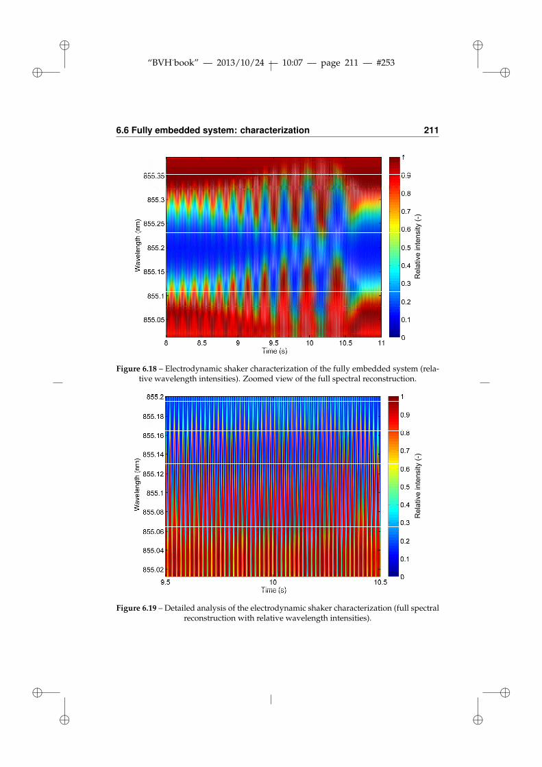
ii
“BVH˙book” — 2013/10/24 — 10:07 — page 211 — #253 ii
ii
ii
6.6 Fully embedded system: characterization 211
Rel
ativ
e in
tens
ity (
-)
Figure 6.18 – Electrodynamic shaker characterization of the fully embedded system (rela-tive wavelength intensities). Zoomed view of the full spectral reconstruction.
Rel
ativ
e in
tens
ity (
-)
Figure 6.19 – Detailed analysis of the electrodynamic shaker characterization (full spectralreconstruction with relative wavelength intensities).
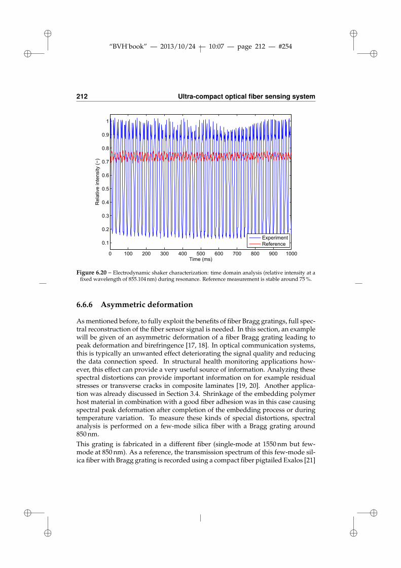
ii
“BVH˙book” — 2013/10/24 — 10:07 — page 212 — #254 ii
ii
ii
212 Ultra-compact optical fiber sensing system
0 100 200 300 400 500 600 700 800 900 1000
0.1
0.2
0.3
0.4
0.5
0.6
0.7
0.8
0.9
1
Rel
ativ
e in
tens
ity (−
)
Time (ms)
ExperimentReference
Figure 6.20 – Electrodynamic shaker characterization: time domain analysis (relative intensity at afixed wavelength of 855.104 nm) during resonance. Reference measurement is stable around 75 %.
6.6.6 Asymmetric deformation
As mentioned before, to fully exploit the benefits of fiber Bragg gratings, full spec-tral reconstruction of the fiber sensor signal is needed. In this section, an examplewill be given of an asymmetric deformation of a fiber Bragg grating leading topeak deformation and birefringence [17, 18]. In optical communication systems,this is typically an unwanted effect deteriorating the signal quality and reducingthe data connection speed. In structural health monitoring applications how-ever, this effect can provide a very useful source of information. Analyzing thesespectral distortions can provide important information on for example residualstresses or transverse cracks in composite laminates [19, 20]. Another applica-tion was already discussed in Section 3.4. Shrinkage of the embedding polymerhost material in combination with a good fiber adhesion was in this case causingspectral peak deformation after completion of the embedding process or duringtemperature variation. To measure these kinds of special distortions, spectralanalysis is performed on a few-mode silica fiber with a Bragg grating around850 nm.This grating is fabricated in a different fiber (single-mode at 1550 nm but few-mode at 850 nm). As a reference, the transmission spectrum of this few-mode sil-ica fiber with Bragg grating is recorded using a compact fiber pigtailed Exalos [21]

ii
“BVH˙book” — 2013/10/24 — 10:07 — page 213 — #255 ii
ii
ii
6.6 Fully embedded system: characterization 213
SLED and an Agilent 86142B OSA, shown in Figure 6.21.
856 856.2 856.4 856.6 856.8 857 857.2 857.4 857.6 857.8−60
−58
−56
−54
−52
−50
−48
−46
−44
Wavelength (nm)
Inte
nsity
(dB
m)
Figure 6.21 – Fiber Bragg grating in transmission using an SLED and an OSA.
The sensing fiber is then clamped between two stages accommodated with micro-screws to apply a strain on the Bragg grating. The fully embedded interrogationscheme is again using the modulation mode, as discussed in Section 6.3. Driv-ing the VCSEL is done using a 1 kHz sawtooth current signal and the VCSEL ismodulated between 2 mA and 4 mA. A linear relation between electrical currentand VCSEL wavelength is assumed. The photocurrent signal (a measure of thetransmitted optical power) is amplified in a negative feedback loop and filtered(read-out filter cut-off frequency = 1 MHz) to clear the signal from high-frequencynoise. A National Instruments data acquisition (DAQ) board is used to read outand store the functional photocurrent data and the DAQ read-out frequency isset at 105 samples per second. Consequently, every millisecond a new spectralwaveform is available and each waveform consists of 100 data points.The total VCSEL tuning range is 1.783 nm yielding a spectral resolution accuracyof 17.83 pm. This wavelength tuning range is deviating from previously men-tioned wavelength ranges at 1 kHz. This is because the VCSEL used for thesetests was originating from a different batch and, as mentioned before, one of thedrawbacks of the VCSELs are the chip-to-chip and batch-to-batch varying opticalcharacteristics. Increasing the VCSEL modulation or photodetector sampling fre-quency can further enhance time and spectral resolution of the system. The upperlimit for the modulation frequency in this simple approach was experimentallydetermined around 20 kHz. Beyond this limit, the wavelength-current relation-

ii
“BVH˙book” — 2013/10/24 — 10:07 — page 214 — #256 ii
ii
ii
214 Ultra-compact optical fiber sensing system
ship of the VCSEL starts to fade. By using pulse width modulation or other moreadvanced signal processing techniques, one could further enhance the resolutionvalues.A calibration measurement is necessary in order to filter the optical power fluctu-ations and to come up with relative wavelength intensities. During the functionaltest, a manual strain of 0.954 mε is applied by loading the fiber with a microscrewwith a resolution of 10 µm. The relative wavelength intensities are color plottedas a function of time in Figure 6.22. This figure displays a dynamic measurementof the fiber Bragg grating during manual straining and releasing of the fiber. Thedifferent straining and releasing steps are clearly visible.
0 0.2 0.4 0.6 0.8 10
0.1
0.2
0.3
0.4
0.5
0.6
0.7
0.8
0.9
1
0.1
0.2
0.3
0.4
0.5
0.6
Rel
ativ
e in
tens
ity (
-)
Figure 6.22 – Dynamic measurement of the fiber Bragg grating using the fully embeddedsystem (wavelength intensity versus time).
In order to experimentally verify the strain which is applied, the minimum wave-length intensity is tracked. A maximum wavelength shift of ≈ 0.7 nm is obtainedat t = 12.96 s. Comparing this value to the theoretical strain of 0.954 mε indicatesan almost perfect transfer of the applied displacement to strain on the fiber. Moreadvanced analysis of the spectral response of the fiber Bragg grating is now pos-sible on a very accurate scale, both in time and wavelength domain. A snapshotof the optical spectrum is shown in Figure 6.23. One can extract the shift in peakwavelength but also other information, not measurable with traditional peak-tracking systems, such as peak deformation or the introduction of birefringenceleading to the two different dips in the optical spectrum (Figure 6.22, t = 7 s and
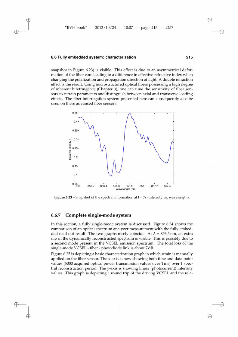
ii
“BVH˙book” — 2013/10/24 — 10:07 — page 215 — #257 ii
ii
ii
6.6 Fully embedded system: characterization 215
snapshot in Figure 6.23) is visible. This effect is due to an asymmetrical defor-mation of the fiber core leading to a difference in effective refractive index whenchanging the polarization and propagation direction of light. A double refractioneffect is the result. Using microstructured optical fibers possessing a high degreeof inherent birefringence (Chapter 3), one can tune the sensitivity of fiber sen-sors to certain parameters and distinguish between axial and transverse loadingeffects. The fiber interrogation system presented here can consequently also beused on these advanced fiber sensors.
856 856.2 856.4 856.6 856.8 857 857.2 857.40.05
0.1
0.15
0.2
0.25
0.3
0.35
0.4
0.45
Wavelength (nm)
Rel
ativ
e in
tesi
ty (−
)
Figure 6.23 – Snapshot of the spectral information at t = 7s (intensity vs. wavelength).
6.6.7 Complete single-mode system
In this section, a fully single-mode system is discussed. Figure 6.24 shows thecomparison of an optical spectrum analyzer measurement with the fully embed-ded read-out result. The two graphs nicely coincide. At λ = 856.5 nm, an extradip in the dynamically reconstructed spectrum is visible. This is possibly due toa second mode present in the VCSEL emission spectrum. The total loss of thesingle-mode VCSEL - fiber - photodiode link is about 7 dB.Figure 6.25 is depicting a basic characterization graph in which strain is manuallyapplied on the fiber sensor. The x-axis is now showing both time and data pointvalues (5000 acquired optical power transmission values over 1 ms) over 1 spec-tral reconstruction period. The y-axis is showing linear (photocurrent) intensityvalues. This graph is depicting 1 round trip of the driving VCSEL and the rela-

ii
“BVH˙book” — 2013/10/24 — 10:07 — page 216 — #258 ii
ii
ii
216 Ultra-compact optical fiber sensing system
854.7 855.1 855.5 855.9 856.3
−5
−4
−3
−2
−1
0
Rel
ativ
e in
tens
ity [d
B]
Wavelength [nm]
Fully embeddedsystemOptical SpectrumAnalyzer
Figure 6.24 – Measuring a single-mode fiber Bragg grating: OSA vs. fully embeddedsystem.
tive intensity values start to saturate from t = 0.3 ms. This effect has nothing todo with the fiber sensor but can be attributed to the fact that higher time valuescorrespond with increasing VCSEL driving currents (Figure 6.3). These increas-ing driving currents are in this case causing an increasing but flattening opticalpower (rather than a linear increase, probably due to thermal effects) explainingthe saturated relative intensity values.
6.6.8 Temperature influence
As discussed in Chapter 2, one of the important advantages associated with sen-sors based on fiber Bragg gratings is their insensitivity to optical intensity fluctu-ations caused by aging effects, deteriorating coupling alignments or differencesin electrical driving currents. Unwanted wavelength fluctuations, for example ofthe driving VCSEL source, can however influence and potentially also compro-mise the sensor measurements. The main reason for these unwanted wavelengthfluctuations is to be found in ambient temperature variations. To check the vul-nerability of the embedded single-mode VCSELs to such ambient temperaturechanges, the emitting wavelength was monitored between 20 C and 70 C usingdifferent driving currents (2.5 mA and 6 mA). An ultra-thin VCSEL package wastherefore mounted on a hot plate and the wavelength was monitored using anAgilent 86142B OSA. The results are shown in Figure 6.26.

ii
“BVH˙book” — 2013/10/24 — 10:07 — page 217 — #259 ii
ii
ii
6.6 Fully embedded system: characterization 217
0 / 0 1000 2000 3000 4000 5000
0.2
0.4
0.6
0.8
Rel
ativ
e in
tens
ity
[−]
Datapoints [−]Time [ms] / 0.2 / 0.6 /0.4 / 0.8 / 1.0 /
start
strain
Figure 6.25 – Characterization of the fully single-mode system: initial measurement vs.strain.
20 30 40 50 60 70854
856
858
860
862
Wav
elen
gthy
[nm
]
Temperaturey[°C]
Iy=y2.5ymAIy=y6ymA
yy=y852.87y+y0.0657yx
yy=y854.60y+y0.0824yx
R2y=y0.999
R2y=y0.996
Figure 6.26 – Wavelength - temperature sensitivity of the single-mode VCSEL source.

ii
“BVH˙book” — 2013/10/24 — 10:07 — page 218 — #260 ii
ii
ii
218 Ultra-compact optical fiber sensing system
Sensitivities of respectively 66 ± 1.2 pm/C and 82 ± 2.7 pm/C are extracted.The typical temperature dependency of the emitting wavelength is 60 pm/C ac-cording to the manufacturer datasheet. An elegant way to circumvent this tem-perature sensitivity could be matching the temperature sensitivity of the embed-ded fiber sensor(s) (Table 3.13) to the sensitivity of the driving VCSEL.
6.7 Conclusion
This chapter described a new fiber sensor interrogation system which can befabricated ultra-small and fully embedded in a thin polymer stack. The sens-ing elements are manufactured using mature and commercially available Bragggrating inscription technology. Driving and read-out electronics and optoelec-tronics were combined with an Android based acquisition unit resulting in aportable and compact sensing system. Furthermore, technology was providedto take the integration a step further and embed the optoelectronics on a chiplevel to obtain a wearable system with a thickness below 1 mm. A broad rangeof new applications, including tactile sensing, structural health monitoring andbiomedical systems, can be targeted with this unique sensing concept.The interrogation technique is based on an intelligent VCSEL-photodiode combi-nation. Two interrogation modes are available: constant current mode and mod-ulation mode. In constant current mode, the transmitted optical power is moni-tored at a fixed wavelength with a maximum acquisition rate of 5 kHz. Using themodulation mode offers full spectral reconstruction. The corresponding wave-length resolution is depending on the driving frequency and data acquisition rate,and demonstrated at, but not limited to, 1.5 pm and 4 pm. The wavelength accu-racy is limited by the VCSEL bandwidth and the associated response time variesbetween 1 ms and 10 ms. In terms of resolution and measurement speed, the onlylimit on the sensing system is the driving laser (VCSEL) chip. Increasing the sens-ing system speed will narrow the wavelength range. There is however only onesignal containing full spectral datasets which has to be read out. Compared toconventional spectrometers and other state-of-the-art fiber Bragg grating interro-gation systems this yields a significant advantage as no optical mirrors have to beturned or multiple CCD elements read out.
ii
“BVH˙book” — 2013/10/24 — 10:07 — page 219 — #261 ii
ii
ii
References 219
References
[1] B. Van Hoe, G. Lee, E. Bosman, J. Missinne, S. Kalathimekkad, O. Maskery,D. J. Webb, K. Sugden, P. Van Daele, and G. Van Steenberge, “Ultra smallintegrated optical fiber sensing system,” Sensors, vol. 12, no. 9, pp. 12 052–12 069, Sept. 2012.
[2] E. J. Voet, G. Luyckx, I. De Baere, J. Degrieck, J. Vlekken, E. Jacobs, andH. Bartelt, “High strain monitoring during fatigue loading of thermoplas-tic composites using imbedded draw tower fibre bragg grating sensors,” inEmboding Intelligence in Structures and Integrated Systems, ser. Advances inScience and Technology, P. Vincenzini and F. Casciati, Eds., vol. 56, 2009, pp.441–446, 3rd International Conference on Smart Materials, Structures andSystems, Acireale, Italy, JUN 2008.
[3] G. Luyckx, E. Voet, N. Lammens, and J. Degrieck, “Strain measurementsof composite laminates with embedded fibre bragg gratings: Criticism andopportunities for research,” Sensors, vol. 11, no. 1, pp. 384–408, Jan. 2011.
[4] G. Meltz, W. Morey, and W. Glenn, “Formation of bragg gratings in opticalfibers by a transverse holographic method,” Optics Letters, vol. 14, no. 15, pp.823–825, Aug. 1989.
[5] Y. Huang, T. Guo, C. Lu, and H.-Y. Tam, “Vcsel-based tilted fiber gratingvibration sensing system,” IEEE Photonics Technology Letters, vol. 22, no. 16,pp. 1235–1237, Aug. 2010.
[6] C. F. R. Mateus and C. L. Barbosa, “Harsh environment temperature andstrain sensor using tunable vcsel and multiple fiber bragg gratings,” in 2007SBMO/IEEE MTT-S INTERNATIONAL MICROWAVE AND OPTOELEC-TRONICS CONFERENCE, VOLS 1 AND 2, 2007, pp. 496–498, sBMO/IEEEMTT-S International Microwave and Optoelectronics Conference, Salvador,Brazil, OCT-NOV 2007.
[7] F. Koyama, “Recent advances of vcsel photonics,” Journal of Lightwave Tech-nology, vol. 24, no. 12, pp. 4502–4513, Dec. 2006.
[8] K. Zogal, T. Gruendl, H. A. Davani, C. Gierl, S. Jatta, C. Grasse, M. C. Amann,and P. Meissner, “High speed modulation of a 1.55-mu m mems-tunablevcsel,” in CONFERENCE ON LASERS AND ELECTRO-OPTICS (CLEO),2011, conference on Lasers and Electro-Optics (CLEO), Baltimore, MD, MAY2011.
[9] M. Njegovec and D. Donlagic, “High-resolution spectrally-resolved fiber op-tic sensor interrogation system based on a standard dwdm laser module,”Optics Express, vol. 18, no. 23, pp. 24 195–24 205, Nov. 2010.
ii
“BVH˙book” — 2013/10/24 — 10:07 — page 220 — #262 ii
ii
ii
220 Ultra-compact optical fiber sensing system
[10] S. Schultz, W. Kunzler, Z. Zhu, M. Wirthlin, R. Selfridge, A. Propst, M. Zikry,and K. Peters, “Full-spectrum interrogation of fiber bragg grating sensors fordynamic measurements in composite laminates,” Smart Materials & Struc-tures, vol. 18, no. 11, Nov. 2009.
[11] T. Vella, S. Chadderdon, R. Selfridge, S. Schultz, S. Webb, C. Park, K. Peters,and M. Zikry, “Full-spectrum interrogation of fiber bragg gratings at 100 khzfor detection of impact loading,” Measurement Science & Technology, vol. 21,no. 9, SI, Sept. 2010.
[12] Phosfos Consortium. (2008) Photonic skins for optical sensing. [Online].Available: http://www.phosfos.eu/
[13] G. C. B. Lee, B. Van Hoe, Z. Yan, O. Maskery, K. Sugden, D. Webb, andG. Van Steenberge, “A compact, portable and low cost generic interro-gation strain sensor system using an embedded vcsel, detector and fibrebragg grating,” ser. Proceedings of SPIE, C. Lei and K. Choquette, Eds.,vol. 8276, 2012, conference on Vertical-Cavity Surface-Emitting Lasers XVI(VCSELs)/SPIE Photonics West Symposium, San Francisco, CA, JAN 2012.
[14] K. Hill and G. Meltz, “Fiber bragg grating technology fundamentals andoverview,” Journal of Lightwave Technology, vol. 15, no. 8, pp. 1263–1276, Aug.1997.
[15] X. Chen, C. Zhang, B. Van Hoe, D. J. Webb, K. Kalli, G. Van Steenberge,and G. D. Peng, “Photonic skin for pressure and strain sensing,” ser. Pro-ceedings of SPIE-The International Society for Optical Engineering, F. Bergh-mans, A. Mignani, and C. Hoof, Eds., vol. 7726, 2010, conference on OpticalSensing and Detection, Brussels, Belgium, APR 2010.
[16] B. Van Hoe, G. Van Steenberge, E. Bosman, J. Missinne, T. Geernaert,F. Berghmans, D. Webb, and P. Van Daele, “Optical fiber sensors embeddedin polymer flexible foils,” ser. Proceedings of SPIE-The International Societyfor Optical Engineering, F. Berghmans, A. Mignani, and C. Hoof, Eds., vol.7726, 2010, conference on Optical Sensing and Detection, Brussels, Belgium,APR 2010.
[17] R. Gafsi and M. El-Sherif, “Analysis of induced-birefringence effects on fiberbragg gratings,” Optical Fiber Technology, vol. 6, no. 3, pp. 299–323, July 2000.
[18] R. Wagreich, W. Atia, H. Singh, and J. Sirkis, “Effects of diametric load onfibre bragg gratings fabricated in low birefringent fibre,” Electronics Letters,vol. 32, no. 13, pp. 1223–1224, June 1996.
[19] Y. Okabe, S. Yashiro, T. Kosaka, and N. Takeda, “Detection of transversecracks in cfrp composites using embedded fiber bragg grating sensors,”Smart Materials & Structures, vol. 9, no. 6, pp. 832–838, Dec. 2000.

ii
“BVH˙book” — 2013/10/24 — 10:07 — page 221 — #263 ii
ii
ii
References 221
[20] Y. Okabe, S. Yashiro, R. Tsuji, T. Mizutani, and N. Takeda, “Effect of thermalresidual stress on the reflection spectrum from fiber bragg grating sensorsembedded in cfrp laminates,” Composites Part A - Applied Science and Manu-facturing, vol. 33, no. 7, pp. 991–999, 2002.
[21] EXALOS: Superluminescent Light Emitting Diodes (SLEDs) Manufacturer.(Accessed 2013) Products. [Online]. Available: http://www.exalos.com/

ii
“BVH˙book” — 2013/10/24 — 10:07 — page 222 — #264 ii
ii
ii

ii
“BVH˙book” — 2013/10/24 — 10:07 — page 223 — #265 ii
ii
ii
7High resolution pressure sensor based
on optical feedback in a VCSEL
This final technology chapter is reaching out for optical sensor principles which are inher-ent to the optoelectronic sources avoiding the use of any Bragg grating structure. Thesesensors can pave the way towards further sensor miniaturization and integration. Withinthis chapter a highly accurate integrated incremental pressure sensor, based on opticalfeedback in a VCSEL, is developed. This laser chip is again embedded as an unpackagedoptoelectronic component in a polymer host material. A compressible polymer sensinglayer is acting simultaneously as an external laser cavity and as a transducer material,converting the pressure which is applied into a change in the laser cavity length.
7.1 Introduction
As already discussed in Chapter 1, pressure sensors are becoming increasinglyimportant in different areas, such as the automotive industry, the structural healthsector and biomedical engineering. These markets are demanding for technolo-gies which allow to miniaturize sensors and, at the same time, to integrate sensorelements with microelectronic functions in minimal space. Within the medicalapplication domain additional requirements apply such as biocompatibility, me-chanical flexibility and sensor insensitivity to electromagnetic interference.The existing Microelectromechanical Systems (MEMS) pressure sensors are

ii
“BVH˙book” — 2013/10/24 — 10:07 — page 224 — #266 ii
ii
ii
224 High resolution pressure sensor based on optical feedback in a VCSEL
mostly based on piezoresistive or capacitive force sensing technologies [1]. Op-tical alternatives, mostly based on fiber sensors, have been developed by severalinstitutes [2]. Polymer and polymer embedded optical fiber sensors as wellas ultra-small fiber sensing systems have been discussed in Chapters 3 and 6.These sensors can perform absolute pressure measurements and offer uniqueadvantages such as immunity to electromagnetic interference and capability ofoperating in harsh environments. In this chapter, an optical, incremental, VCSELbased sensor is presented based on self-mixing interferometry in an external lasercavity. Using unpackaged laser chips, one can embed this sensor element in anultra-thin flexible package (an optical sensing foil) which can be mounted on anon-planar surface or even irregularly shaped objects, such as a the human body.These laser chips typically contain arrays of VCSELs (pitch between the lightemitting areas of 250 µm for example) enabling high-density measurements insmall areas. In this respect the VCSEL sensing approach is clearly distinguishablefrom the (multiplexed) optical fiber sensors, typically covering larger areas butwith lower density.The working principles of optical sensors based on self-mixing interferometrywere discussed in Chapter 2, Section 2.1.2. In the next paragraph, these work-ing principles are applied on VCSEL array chips. This VCSEL based pressuresensor combines the specific advantages of sensors based on an optical sensingmechanism with extensive integration capabilities. The pressure sensor which isdeveloped within this chapter namely relies on optical feedback in the optoelec-tronic component itself. Expensive and delicate fiber coupling or free-space lightcoupling technology blocks are consequently avoided.
7.2 Principle of operation
The pressure sensing mechanism is based on a displacement measurement ofan external target on a VCSEL chip. The underlying mechanism for this dis-placement measurement is based on the self-mixing interference effect in VCSELswhich is observed when a fraction of light emitted from the laser is injected backinto the laser cavity. This back reflection is performed by an external target on adistance Lext from the VCSEL emitting area [3]. As a result, an external cavity iscreated between the VCSEL and the external reflector (Figure 7.1).The VCSEL resonator itself consists of two Distributed Bragg Reflector (DBR) mir-rors parallel to the wafer surface with an active region consisting of one or morequantum wells for the laser light generation in between. The planar DBR-mirrors(reflectance Rint, Figure 7.1) consist of layers with alternating high and low re-fractive indices. Each layer has a thickness of a quarter of the laser wavelengthin the material, yielding intensity reflectivities above 99 %. High reflectivity mir-rors are required in VCSELs to balance the short axial length of the gain region.

ii
“BVH˙book” — 2013/10/24 — 10:07 — page 225 — #267 ii
ii
ii
7.2 Principle of operation 225
The external target has a reflecting layer with a reflectance Rext and is typicallyconsisting of a thin metal layer.Due to the coherence of the emitted laser light, the recoupled light mixes in adeterministic way with the light in the internal laser cavity. The phase shift in-troduced by the round trip travel to and from the target, influences the optoelec-tronic characteristics of the laser. Depending on the delay and the phase of theback-reflected light, the VCSEL threshold condition is varied; thus the emittedoptical power changes as the pump current is held constant. The change in thethreshold implies a change in the actual VCSEL carrier density; as a consequence,the wavelength emitted by the VCSEL subject to back reflections is also slightlyvaried [3, 4]. Because of this phase shift dependency, increasing or decreasing Lextresults in a periodic variation of laser wavelength, optical power and electrical re-sistance, all with period λ/2 (λ being the emitting wavelength of the VCSEL, inthis chapter 850 nm). This means that the target displacement can be calculatedby monitoring the periodic signal between the initial and the final position of thetarget, where the spacing between the two consecutive peaks corresponds to thedistance of λ/2. Similar interferometric effects in VCSELs can be used to senseother parameters or even perform multi-parametric sensing [5].
VCSEL L
Lext
Rext
External cavity
Rint
Rint
w(z)
θ
w0
zR
w02
z
Target
Figure 7.1 – Schematic overview of the VCSEL sensor principle.
7.2.1 Transducer layer parameters
A parameter of major importance for the sensor discussed in this chapter is theexternal cavity material (Figure 7.1). Most existing sensors based on self-mixinginterference working principles are based on air as an external cavity materialbetween the light source and the target. Light is in this case propagating free-space and optical elements (lenses) are typically needed to observe self-mixinginterferometry. In the first part of this chapter, a free-space optical path is indeedused as an external cavity for discrete experiments producing proof-of-principle

ii
“BVH˙book” — 2013/10/24 — 10:07 — page 226 — #268 ii
ii
ii
226 High resolution pressure sensor based on optical feedback in a VCSEL
results and demonstrating the sensor capabilities. In this case displacement mea-surements are performed rather than real pressure measurements.The sensing mechanism of the integrated pressure sensor discussed in the secondpart of this chapter is based on a conversion of the applied pressure to a certaindisplacement of the external target mirror layer. This target reflecting layer itselftypically consists of a thin, little compressible, metal structure. Therefore, a keysensor parameter determining to a large extent the sensing range and the accord-ing accuracy, is the external cavity material. This transducer material is situatedbetween the VCSEL (internal laser cavity) and the external target (Figure 7.2). Itsmechanical properties are tuning the sensor characteristics (sensing range, accu-racy, sensitivity, etc.).The reason why unpackaged VCSEL components and extensive integration pro-cesses are used, is the possibility to integrate the sensor component (VCSEL) in anultra-thin polymer package. To preserve the advantages associated with this inte-grated approach in terms of size and flexibility, an integrated polymer transducerlayer is replacing the air gap. It is clear that without this integration technology,the sensor concept from Figure 7.2 would not be possible.
VCSEL array chip
reflecting layer(external target)
Ultra thin flexible VCSEL package
PDMS transducer layer
Pressure
Figure 7.2 – Schematic overview of the integrated VCSEL sensor principle.
The transducer material for the integrated sensor approach is a compressiblepolydimethylsiloxane (PDMS) material, Sylgard®184, throughout the entirechapter. As mentioned before (Chapter 3, Section 3.3), it is difficult to list ex-act mechanical properties of PDMS as they are depending on the preparationconditions of the material but also the application methods and curing param-eters. As a guideline, the Young’s modulus E typically varies between 0.7 and3.7 MPa and Poisson’s ratio ν ≈ 0.5. Next to its mechanical flex- and stretcha-

ii
“BVH˙book” — 2013/10/24 — 10:07 — page 227 — #269 ii
ii
ii
7.2 Principle of operation 227
bility, PDMS exhibits good environmental and thermal stability up to 300 C [6].Furthermore, the material shows a relatively low moisture absorption and is re-sistant to a large range of commonly used chemicals [7]. For a detailed discussionon the mechanical and optical properties of PDMS, the reader is again referred tothe PhD dissertation of Jeroen Missinne [8] (Chapter 2, Section 2.4).
7.2.2 Interferometric parameters
During all experiments based on self-mixing interferometry the following impor-tant interferometric parameters, determining the working regime of the VCSELsensor, have to be monitored:
• The recoupled optical power Pcoupled. This value is depending on severalVCSEL parameters such as the aperture, divergence angle and Rayleighlength, but also external cavity parameters such as the cavity length andmaterial, as well as the reflecting layer hedging the external cavity.
• The feedback parameter C. This value is determined by the (internal) VCSELlinewidth enhancement factor, the laser internal DBR reflectance, cavitylength and effective refractive index as well as the external cavity length,effective refractive index and external mirror reflectance.
Recoupled optical power
The power Pcoupled which is coupled back in the internal laser cavity after propa-gation through the external cavity length can be estimated assuming the VCSELoutput beam has a Gaussian spatial profile. A schematic view was shown in Fig-ure 7.1. The optical power P passing through a circle of radius r in the transverseplane at position z is
P(r, z) = P0
(1− e−2r2/w2(z)
)where P0 is the total power transmitted by the beam. For a Gaussian beam prop-agating in free-space, the spot size radius w(z) will be at a minimum value w0 atone place along the beam axis, known as the beam waist. For a beam of wave-length λ at a distance z along the beam from the beam waist, the variation of thespot size is given by [9]
w(z) = w0
√1 +
(z
zR
)2
where the origin of the z-axis is defined, without loss of generality, to coincidewith the beam waist, and where [9]

ii
“BVH˙book” — 2013/10/24 — 10:07 — page 228 — #270 ii
ii
ii
228 High resolution pressure sensor based on optical feedback in a VCSEL
zR =π w2
0λ
is called the Rayleigh range. The VCSEL which is used as a sensor element is amultimode 850 nm component from ULM Photonics [10]. From Chapter 4, thefollowing VCSEL parameters are obtained
λ = 850 nm
P0|V=1.5 V = 0.5 mW
w0 ≈ 5 µm
dP0
dV≈ 11.3
mWV
Based on these values and under the assumption that the light is traveling oneround trip (2 Lext) to recouple into the internal laser cavity, Pcoupled can be calcu-lated as a function of the external cavity length Lext using neff,ext = 1.41 @ 850 nm.This is shown graphically for different VCSEL driving voltages in Figure 7.3.
10−3 10−2 10−1 100 101 10210−7
10−5
10−3
10−1
101
P coup
led [m
W]
Lext [mm]
1.5 V1.6 V1.7 V1.8 V
Figure 7.3 – Optical power coupled back into the laser cavity versus the external cavitylength for varying VCSEL driving voltages.
A first observation from Figure 7.3 is that starting from 100 µm, the recoupled op-tical power is dropping drastically. From Chapter 2, Section 2.1.2, we know that

ii
“BVH˙book” — 2013/10/24 — 10:07 — page 229 — #271 ii
ii
ii
7.2 Principle of operation 229
the VCSEL parameters are dynamically modulated because of the self-mixing ef-fect starting from a recoupled optical power of Pcoupled = 0.01 P0, leading to thefollowing condition for observing self-mixing interferometry effects:
Lext < 901 µm
Optical feedback parameter
A conventional VCSEL interferometric self-mixing configuration was shown inFigure 7.1. This configuration is equivalent to a three-mirror cavity, where theback-diffused or back-reflected power by the remote target can be calculated as afraction Rext of the emitted optical power P0. An analytical steady-state solutiondescribing the optical power in this three-mirror laser cavity can be found in [4,11, 12], and is leading to the following general expression for the optical poweremitted by the total VCSEL structure (including the external cavity)
P(φ) = P0(1 + m F(φ))
where again P0 is the power emitted by the unperturbed VCSEL, m is the modula-tion index and F(φ) is a periodic function of the interferometric phase φ = 2 k Lext(k = 2π λ), of period 2π [3]. The modulation index m and the shape of the func-tion F(φ) depend on the so-called feedback parameter C.This feedback parameter is defined as follows [3, 4]
C =κ
ττext
√1 + α2
α is the VCSEL linewidth enhancement factor and κ is the feedback coefficientgiven by
κ = (1− Rint)
√Rext
Rint.
Rint is the reflectance for the internal DBR VCSEL layers and Rext is the reflectanceof external cavity reflecting layer (as shown in Figure 7.1). τ and τext are theround-trip propagation time in the laser cavity (length L) and the external cavity(length Lext) respectively
τ =2 neff L
c
τext =2 neff,ext Lext
c.

ii
“BVH˙book” — 2013/10/24 — 10:07 — page 230 — #272 ii
ii
ii
230 High resolution pressure sensor based on optical feedback in a VCSEL
neff and neff,ext are the effective refractive indexes in respectively the internal andexternal laser cavity and c is the speed of light.Thus, the value of the C parameter depends on both the amount of feedbackand, interestingly, on target distance Lext. The feedback parameter is of greatimportance, because it discriminates between different feedback regimes:
• For C 1, we have the very weak feedback regime. F(φ) is a cosine func-tion and the modulation index m is proportional to
√Rext.
• For 0.1 < C < 1, we have the weak feedback regime. The function F(φ)gets distorted, showing a non-symmetrical shape; the modulation index mis again proportional to
√Rext.
• For 1 < C < 4.6, we have the moderate feedback regime. The function F(φ)becomes three-valued for certain values of the phase φ, i.e. the system isbistable, with two stable states and one unstable. The modulation index mincreases for increasing
√Rext, but it is no longer proportional to it. The
interferometric signal becomes sawtooth-like and exhibits hysteresis.
• For C > 4.6, we have the strong feedback regime. The function F(φ) maybecome five-valued, not all the specimens of VCSELs remain in the self-mixing regime; rather, in some cases the VCSEL enters the mode-hoppingregime and interferometric measurements are no longer possible.
Introducing asymmetry in the VCSEL interference enables the determinationof the displacement direction. Therefore, the feedback parameter is preferablylarger than 0.1. Together with the restriction at the upper side of the feedbackparameter, a functional range of 0.1 < C < 4.6 is obtained.The feedback parameter is calculated as a function of the external cavity length(Figure 7.4) in the case of air as an external cavity and in the case of Sylgard®184as an external cavity, each time with a gold reflecting layer on top (Au coating >skin depth). The conversion of external pressure into displacement will be guar-anteed by the use of this compressible PDMS layer as an external cavity which isapplied on top of an ultra-thin flexible VCSEL package (Figure 7.2).To end up with a feedback parameter within the functional range between 0.1and 4.6, the following condition is obtained for air acting as an external cavitymaterial:
18 µm < Lext < 800 µm
To end up with a feedback parameter between 0.1 and 4.6, the following conditionis obtained for Sylgard®184 acting as an external cavity material:
13 µm < Lext < 570 µm

ii
“BVH˙book” — 2013/10/24 — 10:07 — page 231 — #273 ii
ii
ii
7.3 Discrete proof-of-principle set-up 231
10−3 10−2 10−1 100 101 102
10−2
10−1
100
101
102
103
Feed
back
par
amet
er C
[−]
Lext [mm]
air cavitySylgard® 184 cavity
Figure 7.4 – Optical feedback parameter for different external cavity lengths and differentexternal cavity materials.
7.3 Discrete proof-of-principle set-up
A discrete set-up was developed to mimic and prove the working principle of thisnew integrated sensing mechanism. This proof-of-principle set-up is schemati-cally shown in Figure 7.5 and consists of different building blocks which are readout in parallel by a PC through GPIB. An unpackaged wire bonded VCSEL wasput on a fixed location and a movable reflector acting as the external target (Rext)was positioned close to the active area. This movable reflector consisted of a coat-ing layer of evaporated gold on top of a multimode silica fiber with a 62.5 µm corediameter. This fiber was clamped on a precision microstage and connected to anoptical power meter. The external cavity consequently consisted of an air gapbetween the light emitting area of the VCSEL (∆z = 0) and the movable reflector(∆z = Lext). The electrical parameters of the VCSEL were driven and read outthrough a Source Measure Unit (SMU).Figure 7.6 is showing an overview of the full measurement set-up (top), a detailedview on the fiber alignment on top of the VCSEL light emitting area using CCDcameras (middle) and the actual view of the cameras on the wire bonded VCSELand Au coated fiber facet (bottom).It is important to mention that the ULM Photonics VCSEL which is used for theremainder of this chapter is a 850 nm multimode VCSEL array with top-top con-tacts. These VCSELs typically emit only one mode up to a driving current of

ii
“BVH˙book” — 2013/10/24 — 10:07 — page 232 — #274 ii
ii
ii
232 High resolution pressure sensor based on optical feedback in a VCSEL
1 mA. Increasing the VCSEL current will induce a higher number of modes beingemitted by the VCSEL [13, 14].
Δz
SMU
Power
meter
PM500
Controller
PC
GPIB
GPIB
GPIB
GPIB
photo-
detector
PM500
XYZ stagefixed stage
Lext
Rext (Au coating)
0
optical
fiber
wirebonded
VCSEL
Figure 7.5 – Schematic view of the discrete proof-of-principle set-up.
7.3.1 Time domain results
Moving the fiber reflector 4 times over 5 µm using displacement steps of 50 nmresults in a periodic variation of both the monitored optical power and electricalVCSEL driving current while the VCSEL voltage is kept constant. A Keithley 2400SMU is used to control the VCSEL junction voltage and read out the VCSEL driv-ing current. The resulting electrical and optical power fluctuations for a VCSELdriving voltage of 1.5 V are shown in Figure 7.7. A reference measurement (reflec-tor is not moving) is included for all measurements. From Figure 7.7b, the firsttrend we observe in the experimental signal is a slow optical power variationcoinciding with the displacement variation shown in Figure 7.7a. The larger theexternal cavity length is, the less power is coupled to the optical fiber. The secondtrend we observe is a fast periodical variation due to the optical feedback effectand superimposed on the slower optical power variation. A total of roughly 48periods can be observed, demonstrating the 425 nm (λ/2) periodicity. The opticalpower signal is oscillating with a peak-to-peak variation of 10 nW. The informa-tion we can extract on the exact periodical shape of the waveform is rather limitedas the data acquisition speed is limited to roughly 7 points each interferometricperiod. The electrical current signal (Figure 7.7c) is not showing any significantdifference between the reference and the experimental measurement. Probablythe optical feedback power is too low to modulate the electrical parameters.

ii
“BVH˙book” — 2013/10/24 — 10:07 — page 233 — #275 ii
ii
ii
7.3 Discrete proof-of-principle set-up 233
The same measurement is repeated with a driving VCSEL voltage of 1.6 V (Fig-ure 7.8). Variations in the optical power (Figure 7.8b) show a similar behavior asfor the previous measurements although some higher harmonic effects are visi-ble, possibly due to the multimodal behavior of the VCSEL. The electrical currentmeasurement (Figure 7.8c) however now exhibits a similar modulated behaviorconfirming the ability to read out the VCSEL interference effect through the elec-trical current.When further increasing the VCSEL driving voltage to 1.7 V (Figure 7.9), a similarVCSEL behavior is observed both for the optical power and electrical current. Thepeak-to-peak variation is 8 µW for the experimental measurements in Figure 7.8band 7.9b, and 8 µA for the experimental measurements in Figure 7.8c and 7.9c.
7.3.2 Frequency domain results
To evaluate in detail how the experimental optical power and electrical currentvariations relate to the theoretical periodicity of 425 nm, frequency analysis is per-formed on the time domain results. Therefore the optical power/electrical cur-rent values corresponding to the same displacement position are averaged outresulting in unambiguous power and current versus displacement values. Thelinear trend is removed from the experimental signals and zero-padding (210)is applied to increase the resolution in the frequency domain. The sample fre-quency is the inverse of one displacement step of the stage in the time domain( fs = 1/50 nm). A Fast Fourier Transform (FFT) operation is applied on theresulting datasets and the power spectral density information is consequentlyextracted. The results are shown in Figure 7.10. The Full Width at Half Maxi-mum (FWHM) is similar for all measurements, ≈ 0.24 µm−1. Determining themaximum values for all the averaged measurements yields the reciprocal inter-ferometric signal period. These calculated periods of the analyzed interferometricsignals at different driving voltages are depicted in Table 7.1 and are varying be-tween 403 nm and 410 nm, slightly lower than the expected 425 nm. Because ofthe low sample frequency and the translation stage inaccuracies, these values aredefinitely acceptable.
Table 7.1 – Frequency analysis of the discrete proof-of-principle results.
Measured quantity Driving voltage Reciprocal interferometric signal period
Optical power 1.5 V 406 nmElectrical current 1.5 V -Optical power 1.6 V 403 nmElectrical current 1.6 V 406 nmOptical power 1.7 V 406 nmElectrical current 1.7 V 410 nm

ii
“BVH˙book” — 2013/10/24 — 10:07 — page 234 — #276 ii
ii
ii
234 High resolution pressure sensor based on optical feedback in a VCSEL
Figuur 4.13: Verwezenlijking van de niet-ingebedde experimentele opstelling met een multimodevezel voorzien van een fijne goudlaag als externe reflector en de alignatie ervan
64
Figure 7.6 – Discrete proof-of-principle set-up. (top) Overview of the full measurement set-up. (mid-dle) Fiber alignment on light emitting area of the vertically mounted VCSEL. (bottom) Camera view on
the wire bonded VCSEL and fiber mirror facet.

ii
“BVH˙book” — 2013/10/24 — 10:07 — page 235 — #277 ii
ii
ii
7.3 Discrete proof-of-principle set-up 235Δ
(a) Position of the movable reflector which was mounted on a microstage.
0 100 200 300 4000.075
0.08
0.085
0.09
P [µ
W]
Time [s]
ExperimentReference
(b) Variations in the optical power.
0 100 200 300 4000.7212
0.7215
0.7218
0.7221
I VC
SEL [m
A]
Time [s]
ExperimentReference
(c) Variations in the electrical current.
Figure 7.7 – Discrete proof-of-principle result with a VCSEL driving voltage of 1.5 V.

ii
“BVH˙book” — 2013/10/24 — 10:07 — page 236 — #278 ii
ii
ii
236 High resolution pressure sensor based on optical feedback in a VCSELΔ
(a) Position of the movable reflector which was mounted on a microstage.
0 100 200 300 40028
32
36
40
P [µ
W]
Time [s]
ExperimentReference
(b) Variations in the optical power.
0 100 200 300 4002.792
2.796
2.8
2.804
2.808
I VC
SEL [m
A]
Time [s]
ExperimentReference
(c) Variations in the electrical current.
Figure 7.8 – Discrete proof-of-principle result with a VCSEL driving voltage of 1.6 V.

ii
“BVH˙book” — 2013/10/24 — 10:07 — page 237 — #279 ii
ii
ii
7.3 Discrete proof-of-principle set-up 237Δ
(a) Position of the movable reflector which was mounted on a microstage.
0 100 200 300 400
65
70
75
80
P [µ
W]
Time [s]
ExperimentReference
(b) Variations in the optical power.
0 100 200 300 4005.475
5.478
5.481
5.484
5.487
I VC
SEL [m
A]
Time [s]
ExperimentReference
(c) Variations in the electrical current.
Figure 7.9 – Discrete proof-of-principle result with a VCSEL driving voltage of 1.7 V.

ii
“BVH˙book” — 2013/10/24 — 10:07 — page 238 — #280 ii
ii
ii
238 High resolution pressure sensor based on optical feedback in a VCSEL
0 2 4 6 80
0.5
1
1.5 x 10⁻⁶
Pow
er sp
ectru
m [A
.U.]
Frequency [µm−1]
AverageStandard deviation
(a) Optical power at 1.5 V:power spectral density.
0 2 4 6 80
0.5
1
1.5
2 x 10⁻³
Pow
er sp
ectru
m [A
.U.]
Frequency [µm−1]
AverageStandard deviation
(b) Electrical current at 1.5 V:power spectral density.
0 2 4 6 80
0.2
0.4
0.6
0.8
1
Pow
er sp
ectru
m [A
.U.]
Frequency [µm−1]
AverageStandard deviation
(c) Optical power at 1.6 V:power spectral density.
0 2 4 6 80
0.5
1
1.5
2
Pow
er sp
ectru
m [A
.U.]
Frequency [µm−1]
AverageStandard deviation
(d) Electrical current at 1.6 V:power spectral density.
0 2 4 6 80
0.4
0.8
1.2
1.6
2
Pow
er sp
ectru
m [A
.U.]
Frequency [µm−1]
AverageStandard deviation
(e) Optical power at 1.7 V:power spectral density.
0 2 4 6 80
0.2
0.4
0.6
0.8
1
Pow
er sp
ectru
m [A
.U.]
Frequency [µm−1]
AverageStandard deviation
(f) Electrical current at 1.7 V:power spectral density.
Figure 7.10 – Frequency analysis of the interferometric read-out signals at different VCSELdriving voltages.

ii
“BVH˙book” — 2013/10/24 — 10:07 — page 239 — #281 ii
ii
ii
7.4 Integrated VCSEL sensor approach 239
7.4 Integrated VCSEL sensor approach
7.4.1 Fabrication
The proposed integrated optical pressure sensor consists of a flexible optoelec-tronic package (an ultra-thin flexible VCSEL package), a deformable PDMS layeracting as an external cavity and a reflecting top layer providing optical feedback,as illustrated in Figure 7.2. To fabricate a flexible and ultra-thin package, the850 nm multimode GaAs VCSEL die (1x4 array with top-top contacts, 250 µmpitch, ULM Photonics) was thinned down to 20 µm and embedded in a flexiblepolymer package of 40 µm thick using a dedicated integration process which wasextensively optimized and characterized in Chapter 4 and [15].This VCSEL package was fabricated on a temporary glass substrate and on theVCSEL package a 50 µm thick PDMS layer, Sylgard®184 from Dow Corning, wasspin-coated (Figure 7.11, package A). To enhance the mechanical robustness, thereflecting copper layer was sputtered on a non-functional flexible package. Afterpatterning the metal layer, a 50 µm thick PDMS layer, Sylgard®184 was spin-coated on top (Figure 7.11, package B). Finally, both the VCSEL and mirror pack-age were released from the glass substrate and the PDMS layers were treated withan air plasma (Diener Pico, 0.8 mbar, 24 s, 190 W, 40 kHz generator). After align-ing the reflecting layers with the VCSEL active areas, both packages were broughtinto contact, creating an irreversible bond and a total transducer layer thicknessof 100 µm, perfectly within the functional range of the transducer thickness val-ues derived in Section 7.2. A similar approach can be used to create other typesof sensors measuring other parameters such as shear force [8, 16].
7.4.2 Characterization of the sensor
The pressure sensor was mechanically characterized by applying a controlleddisplacement with a microtip and simultaneously reading out the correspond-ing force experienced by the tip. During sensing operation, the VCSEL drivingcurrent was held constant and the VCSEL voltage was read out. Monitoring theoptical power and wavelength changes requires additional read-out equipmenteffacing the integration advantages and is therefore avoided. An example of acharacterization set-up is depicted in Figure 7.12 (for illustration purposes only,the integrated reflecting layer is not shown). Characterization tests were per-formed using a nanoindenter Asmec UNAT-M set-up with spherical indentationtips, located at Flamac [17], a division of SIM vzw. Also manual loading andunloading was used to characterize the VCSEL sensor.

ii
“BVH˙book” — 2013/10/24 — 10:07 — page 240 — #282 ii
ii
ii
240 High resolution pressure sensor based on optical feedback in a VCSEL
VCSEL array chip
reflecting layer(external target)
Ultra thin flexible VCSEL package
Ultra thin flexible package
PDMS transducer layer
A
B
Pressure
Figure 7.11 – Schematic overview of the integrated VCSEL sensor principle.
Figure 7.12 – Microscope view of a force applying unit of top of the integrated pressuresensor (reflecting layer not shown).

ii
“BVH˙book” — 2013/10/24 — 10:07 — page 241 — #283 ii
ii
ii
7.5 Integrated VCSEL sensor results 241
7.5 Integrated VCSEL sensor results
7.5.1 Linear displacement variation
Embedded VCSEL arrays are subjected to a linear displacement variation. Thespherical indentation tip (10 µm or 150 µm radius) is actively aligned on top ofthe VCSEL light emitting area. The applied displacement and correspondingmeasured force values for the different indentation tips are shown in Figure 7.13during the indentation and release of the tip. There is a clear difference in mate-rial behavior when using different indentation tips on the compressible sensinglayers.
0 2 4 6 8 10
0
20
40
60
80
100
For
ce [
mN
]
Displacement [µm]
(a) Force-displacement curve with a 10 µm spher-ical indentation tip.
0 2 4 6 8 10
0
50
100
150
200
For
ce [
mN
]
Displacement [µm]
(b) Force-displacement curve with a 150 µmspherical indentation tip.
Figure 7.13 – Linear displacement and corresponding force applied on the integrated pres-sure sensor.
For the initial characterization tests, the 10 µm spherical tip was used and themeasurements were limited to the indentation. The release was not taken intoaccount. Table 7.2 summarizes the relevant integrated measurement parameters.The detailed force-displacement curve is depicted in Figure 7.14. The electricalcurrent is kept constant at 1 mA and the variations in the electrical VCSEL junc-tion voltage were monitored through a Keithley 2400 Source Measure Unit (Fig-ure 7.15a).Roughly 22 periods are visible in the time domain signal and given that 1 pe-riod corresponds to a change in external cavity length of 301 nm (neff,ext = 1.41 @850 nm), an experimentally measured displacement of 6.6 µm is obtained. Thedifference between the actual displacement and the experimentally measured

ii
“BVH˙book” — 2013/10/24 — 10:07 — page 242 — #284 ii
ii
ii
242 High resolution pressure sensor based on optical feedback in a VCSEL
Table 7.2 – Test parameters for the linear displacement experiments.
Parameter Value
Indentation set-up Asmec UNAT-Mnanoindenter
Indentation tip diameter 10 µmIndentation depth 10 µmIndentation position Alignment of indent tip
on the VCSEL active areaVCSEL driving current 1.0 mAMultiplexing OffSampling rate 64 Hz
0 200 400 600 800 10000
2
4
6
8
10
Dis
plac
emen
t ∆z
[µm
]
Time [s]0 200 400 600 800 1000
0
20
40
60
80
100
For
ce [
mN
]
Figure 7.14 – Linear displacement and corresponding force applied on the integrated pres-sure sensor.
value can be explained by a 3.4 µm compression of the polymer embedding lay-ers, including the mirror package with the reflecting layer (Figure 7.11). Thiseffect becomes more important for higher force values.Signal processing, including a low-pass 3th order Butterworth filter and a FFT(details were described in Section 7.3.2) to determine the spatial frequency of thesignal, yields a peak frequency in the power spectrum at 2.27 µm−1 (Figure 7.15b).This spatial peak frequency corresponds to a reciprocal interferometric signal pe-riod of 441 nm whereas the expected theoretical value is 301 nm.

ii
“BVH˙book” — 2013/10/24 — 10:07 — page 243 — #285 ii
ii
ii
7.5 Integrated VCSEL sensor results 243
0 200 400 600 800 1000
1.611
1.612
1.613
1.614
Vol
tage
[V]
Time [s](a) Measuring the electrical voltage variation (2 mV peak-to-peak) while keeping the driv-
ing current constant at 1 mA during a 10 µm indentation.
0 2 4 6 80
1
2
3
Pow
er sp
ectru
m [A
.U.]
Frequency [µm−1](b) Result of frequency analysis performed on the measured VCSEL voltage variation.
Figure 7.15 – Time domain and frequency domain result during a linear displacementvariation experiment on the integrated VCSEL sensor.
From further analysis of the results in Figure 7.15a, a 2 mV peak-to-peak signalvariation can be derived. This yields a displacement responsivity of 4.71 µV/nm.Through the Sylgard®184 Young’s modulus, a pressure reponsivity of 26.2 µV/mbaris obtained.State-of-the-art ultra-thin electronic pressure sensors can for example be based onorganic transistor active matrixes [18], having a typical pressure responsivity of0.022 µA/mbar.

ii
“BVH˙book” — 2013/10/24 — 10:07 — page 244 — #286 ii
ii
ii
244 High resolution pressure sensor based on optical feedback in a VCSEL
7.5.2 Spatial sensing range
The spatial responsivity of the sensor was checked by scanning an indentationmatrix of 7 x 7 sensing points on a total area of 240 µm x 240 µm on the VCSELemitting area (Figure 7.16, left) and using the indentation sphere with a radiusof 150 µm and forces up to 300 mN. The driving current was kept constant at1 mA, the electrical voltage variations were monitored and frequency analysiswas performed as described in the previous section. The resulting spatial peakfrequencies are shown in Figure 7.16, right (linearly interpolated between the 49measuring points) and a peak frequency of 2.52 µm−1 is obtained on top of thelight emitting area. The sensor responsivity has dropped to 50 % at 200 µm fromthe central area.
240 µm
240 µm
7 x 7 indentation matrix
VCSEL light emitting area
Figure 7.16 – Measuring the spatial dependency of the VCSEL sensor.(left) Top view of the VCSEL array with schematic representation of the indentation matrix.
(right) Frequency analysis performed on each indentation point.
7.5.3 Resolution doubling
An interesting phenomenon has been observed during experiments involving adiscrete external mirror instead of the integrated reflecting layer (deposited on anon-functional flexible package, Figure 7.11). This external mirror consists of arigid glass substrate with an evaporated gold layer (10 to 20 nm). Manual load-ing and unloading of different weights on the glass substrate (roughly 1 cm by1 cm) is applied. The multimode VCSEL is driven using voltage steering (1.8 V)and the current is monitored through a GPIB connection with a 11.7 Hz sampling

ii
“BVH˙book” — 2013/10/24 — 10:07 — page 245 — #287 ii
ii
ii
7.5 Integrated VCSEL sensor results 245
frequency. One measurement consists of 2500 samples.The resulting graphs (Figure 7.17) clearly show the time at which pressure is ap-plied (t ≈ 15 s) and the time at which pressure is released (t ≈ 105 s). Due toaging effects of the embedded chips and interconnecting copper tracks, the totalresistance value is also considerably higher than during previous measurements.The first trend which can be observed in Figure 7.17a is a significant increase inthe mean current level after pressure is applied and a slow returning process to-wards its initial value after pressure release. This influence on the VCSEL current(< 1 %) is probably due to a changing resistance when applying a certain pressureand through this action compressing the different layers of the VCSEL stack.
0 40 80 120 160 2001.472
1.476
1.48
1.484
1.488
x 10−3
I VC
SEL [m
A]
Time [s](a) Full measurement.
120 130 140 150 160 170 180
1.48
1.482
1.484
1.486
1.488
x 10−3
I VC
SEL [m
A]
Time [s](b) Detailed view.
Figure 7.17 – VCSEL sensor current response to a pressure step function of 73.53 kPa ap-plied at t ≈ 15 s and released at t ≈ 105 s. The VCSEL driving voltage is 1.8 V.

ii
“BVH˙book” — 2013/10/24 — 10:07 — page 246 — #288 ii
ii
ii
246 High resolution pressure sensor based on optical feedback in a VCSEL
Next to these changes in the DC current level, there are also interferometric ef-fects occurring during the experiment. These effects are hardly visible in the firstpart of the measurement. This is probably due to a high noise level in combina-tion with the fact that the pressure is not applied gradually, but rather imposed asa step function. During pressure release, an interferometric signal is visible (de-tailed view in Figure 7.17b) with a double periodicity. The spacing between 2 pe-riods is gradually increasing after pressure release indicating a hysteresis (mem-ory) effect of the transducer layer. This effect is due to the viscoelastic character ofthe PDMS layer preventing a fast recovery of the sensor. The sensing layer conse-quently has a certain time constant which has to be taken into account, this effectwill be further explained in Section 7.5.5. The double periodicity effect can be ex-plained by the multimodal behavior of the VCSEL (starting from IVCSEL ≈ 1 mA).The signal consists of ≈ 30 double periods, corresponding with ≈ 12.75 µm.
7.5.4 Multiplexing
One of the major advantages associated with the use of VCSEL array chips, is thepossibility to address several VCSELs in parallel enabling different multiplexedsensing nodes on a small area (VCSEL chip size is typically 1 mm by 0.35 mm).Using even larger VCSEL arrays or extending the sensing area to a matrix canlead to extensive multiplexing resulting in distributed pressure sensing. The typ-ical spatial resolution (spacing between 2 sensing points or light emitting areason the chip) is 250 µm.The size of traditional piezoresistive or capacitive tactile sensors in literature typ-ically comprises several millimeters [8] (Chapter 1, Tables 1.3 and 1.5, size of 1sensor). State-of-the-art ultra-thin electronic pressure sensors [18] have a typicalspatial sensing resolution of a few mm.In this paragraph, the 1 x 4 ULM Photonics VCSEL arrays are used to prove themultiplexing principle of operation. To do so, an array of 250 (10 x 25) pressuresensing points with a 50 µm spacing is indented and the corresponding electricalsignals of all VCSELs are monitored simultaneously. The 4 VCSELs are driven inparallel using an electrical current of 6 mA (1.5 mA each) and a resistive load, witha resistance roughly 10 times the resistance of a VCSEL, is put in parallel withall 4 optoelectronic components to equally distribute the current. The voltagevariation of the different VCSELs is read out. An overview of the different testparameters is shown in Table 7.3.The result is a collection of 1000 measurements for a 10 µm indentation. An FFTcalculation is again performed to obtain the information in the frequency domain.The power spectrum graphs are analyzed afterwards and the first peak in the fre-quency domain is recorded. These peak frequency points are then plotted in agraph containing the indentation reference number on the x-axis and the obtainedpeak frequency on the y-axis. An example for the second VCSEL of the array is

ii
“BVH˙book” — 2013/10/24 — 10:07 — page 247 — #289 ii
ii
ii
7.5 Integrated VCSEL sensor results 247
Table 7.3 – Test parameters for the multiplexing measurements.
Parameter Value
Indentation set-up Asmec UNAT-Mnanoindenter
Indentation tip diameter 300 µmIndentation depth 10 µmIndentation position Matrix of 10 x 25 points
ensuring a good coverageof the VCSEL active area
VCSEL driving current 1.5 mAMultiplexing 4 pointsSampling rate 64 Hz
shown in Figure 7.18. The 25 different measurement columns (each column con-tains 10 data points) are plotted in one graph showing increased peak frequenciesbetween indent number 25 and 150, coinciding with the region around the sec-ond laser emitting area. The evolution of the magnitude of the peak frequencyis again a measurand for the spatial responsivity of this one VCSEL sensor (seeSection 7.5.2).The data from Figure 7.18 is now plotted in a three-dimensional plot, again show-ing the indent numbers versus the peak frequency values. Figure 7.19 clearlyshows a Gaussian shape determining the influence of a pressure applied on a lo-cation at a certain distance from the VCSEL light emitting area. The light emittingarea is located at the center of the Gaussian beam, close to coordinate (9,6).Analyzing the data from Figure 7.19, we find that the peak frequency drops to50 % of its maximum value after 3 to 4 measurement points (both in X and Y). Thiscorresponds to a spatial sensitivity range ranging between 150 µm and 200 µm,perfectly in line with Section 7.5.2.In the case of multiplexing, four power spectrum graphs similar to Figure 7.18are obtained. A three-dimensional graph incorporating the maximum frequencyvalues of all 4 VCSELs (plotted on top of each other) is shown in Figure 7.20.Using the information from Figure 7.20 as a calibration input for the VCSEL sen-sor, it is now possible to determine the location and the magnitude of a certainpressure applied on a location within the sensing range of the total VCSEL array(at this moment 1.25 mm x 0.5 mm, but easily expendable to larger areas).Every VCSEL has a radial sensing range of about 400 µm diameter with respectto its emitting middle. The profile of the distribution is nicely Gaussian, meaningthat it can easily be interpolated by software to further enhance the measurement

ii
“BVH˙book” — 2013/10/24 — 10:07 — page 248 — #290 ii
ii
ii
248 High resolution pressure sensor based on optical feedback in a VCSEL
0 50 100 150 200 2500
0.5
1
1.5
2
f max
[µm−
1 ]
Indent number [−]
25 columns
10rows
Figure 7.18 – Peak frequencies for the second VCSEL. The columns of the indentationmatrix are plotted next to each other: column 1 comprises Indent number 1 - 10, column 2
Indent number 11 - 20, etc.
5
10
15
20
25
24
68
100
0.5
1
1.5
2
X [indent number]Y [indent number]
f max
[µm
−1]
0
0.4
0.8
1.2
1.6
2
Figure 7.19 – Peak frequencies for the second VCSEL plotted as an overlay on the inden-tation matrix.

ii
“BVH˙book” — 2013/10/24 — 10:07 — page 249 — #291 ii
ii
ii
7.5 Integrated VCSEL sensor results 249
5
10
15
20
25
24
68
100
0.5
1
1.5
2
X [indent number]Y [indent number]
f max
[µm
−1]
0.4
0.8
1.2
1.6
2
Figure 7.20 – Peak frequencies for all 4 VCSELs plotted as an overlay on the indentationmatrix.
accuracy. Knowing the middle and a couple of points around it can fully recon-struct the beam shape.
7.5.5 Indentation speed
The reaction speed and the time response of the sensor are important parameterswhen using the sensor in real-life applications. The PDMS transducer materiallargely determines the dynamic behavior of the sensor. Because of the PDMSmemory effect (hysteresis) observed in earlier measurements, it is interesting toinvestigate the step response to indentations with varying displacement applica-tion speed. All relevant testing parameters are summarized in Table 7.4 and atypical characterization result including both the indentation and release processis shown in Figure 7.21. Figure 7.22 depicts a detailed view on the 50 s and 100 smeasurements.From Figure 7.21 it can be seen that for the lower indentation speeds, the signalgives proper and repeatable results. At an indentation time of 20 s, the signalstarts to deform with respect to the previously obtained signals. The 10 s inden-tation speed does not at all resemble the first two measurements (100 s and 50 srespectively). This distortion can be partially attributed to a sampling rate whichis too low as the sampling frequency is not over the Nyquist criterion minimumfor the complete signal power spectrum.

ii
“BVH˙book” — 2013/10/24 — 10:07 — page 250 — #292 ii
ii
ii
250 High resolution pressure sensor based on optical feedback in a VCSEL
Table 7.4 – Test parameters for the measurements with varying indentation speed.
Parameter Value
Indentation set-up Asmec UNAT-Mnanoindenter
Indentation tip diameter 300 µmIndentation depth 10 µmIndentation position Array of points
ensuring a good coverageof the VCSEL active area
Indentation time 100 s, 50 s, 20 s, 10 sVCSEL driving current 1.0 mAMultiplexing OffSampling rate 64 Hz
−0.50
0.5
0 2 4 6 8 10
Vol
tage
vari
atio
n[m
V]
Displacement ∆z [µm]8 6 4 2 0
−0.50
0.5
−0.50
0.5
−0.50
0.5
Indentation Release
10 s
20 s
50 s
100 s
Figure 7.21 – Sensor response for a 10 µm indentation with varying indentation times,respectively 100 s, 50 s, 20 s, 10 s.

ii
“BVH˙book” — 2013/10/24 — 10:07 — page 251 — #293 ii
ii
ii
7.5 Integrated VCSEL sensor results 251
5.5 6 6.5 7 7.5 8 8.5 9 9.5 10−1.5
−1
−0.5
0
0.5
Vol
tage
var
iati
on [
mV
]
Displacement ∆z [µm]
50 s100 s
Figure 7.22 – Detailed sensor response for a 10 µm indentation with varying indentationtimes, respectively 100 s and 50 s.
There might be an influence of plastic deformation or creep of the transducermaterial. In the force-displacement curves of the full sensor stack at the higherindentation speeds however, no large deformations can be found. Therefore plas-tic deformation of the PDMS transducer will not be the speed limiting factor.Looking back to the detailed structure of the incremental pressure sensor stack(Figure 7.11), the answer probably lies within the distribution of the total dis-placement within the polymer stack. This sensing stack consists of an ultra-thinPI/SU-8 VCSEL package, a PDMS transducer layer and a an ultra-thin PI/SU-8(non-functional) package acting as a support stack for the external cavity reflect-ing layer. Both SU-8 and PDMS are elastomer materials, belong to the group ofmaterials called viscoelastic polymers and have been used as mechanical springsin sensors and actuators. These materials behave partly as an elastic solid at shorttime range and partly as a viscous liquid at long time range [19]. PDMS is famousfor its excellent elasticity and flexibility among other types of elastomer [20].However, by nature PDMS also possesses some small amount of viscous liq-uid behavior, and exhibits a creeping behavior with time, which may result inhysteresis up to 3 - 7 % of full signal scale. Also SU-8 shows these viscoelasticproperties by measuring the creep (up to 10 %) [21, 22]. Although the creep is infirst order reversible, this hysteresis effect can significantly influence the deviceperformance.Because of this creep time effect, one should always take the possibility into ac-

ii
“BVH˙book” — 2013/10/24 — 10:07 — page 252 — #294 ii
ii
ii
252 High resolution pressure sensor based on optical feedback in a VCSEL
count that the sensor does not fully adapt to the actual deformation. Especiallyin the case of fast changes in the deformation, the applied force is not translatedinto deformation of the underlying VCSEL embedding layers, but rather in en-ergy storage in the material or plastic deformation. We can conclude that for fastapplications the top layer of the VCSEL sensor is not yet stiff enough. Other pro-tective layers, such as harder polymers which have a higher stiffness, should beused to investigate higher indentation speeds.
7.6 Conclusion
A highly accurate integrated incremental pressure sensor sensor was developedbased on optical feedback in an embedded Vertical-Cavity Surface-Emitting laser.This laser chip can be embedded in a polymer host material and an external cav-ity, consisting of a compressible transducer material and a reflecting layer, is ap-plied on top. The transducer layer consists of an external laser cavity of 100 µmon top of the VCSEL light emitting area. The reflecting layer is coupling part ofthe emitted laser light back into the internal VCSEL cavity introducing opticalfeedback and causing self-mixing interferometry. This interference signal adoptsa periodic shape corresponding to half the VCSEL wavelength.By applying pressure and consequently compressing the external cavity and thuschanging the external cavity length, the optical and electrical VCSEL parametersare modulated. The sensing mechanism was first proven using a discrete proof-of-principle set-up and the integrated sensing principle has been demonstratedusing a PDMS transducer layer. Characterization test on this integrated samplewere performed using a nanoindenter. Starting from a 850 nm VCSEL, a sensingdisplacement resolution in the nanometer range was achieved and the responsiv-ity to forces up to 300 mN in a 240 x 240 µm2 matrix was measured resulting ina 2 mV peak-to-peak variation of the electrical driving voltage. More advancedsignal reconstruction techniques can enhance the sensor read-out accuracy.The use of unpackaged VCSELs reduces the sensor dimensions and minimizesthe distance between two adjacent sensing points. By choosing the appropriatetransducer material, a wide range of tactile sensing applications can be targetedwith this sensor. The use of multimode VCSELs is introducing higher-order modeeffects and offers the possibility to further enhance the sensing resolution. TheVCSEL chip arrays have a typical separation distance of 250 µm between two ad-jacent emitting arrays. Scanning multiplexed or even distributed sensing pointsis enabled when reading out several electrical current values in parallel. The spa-tial responsivity of a VCSEL sensor typically shows a Gaussian profile with asensing radius of 200 µm.When using the compressible PDMS layer as a flexible transducer interface, onehas to be careful to take into account the viscoelastic effect of this polymer ma-

ii
“BVH˙book” — 2013/10/24 — 10:07 — page 253 — #295 ii
ii
ii
7.6 Conclusion 253
terial. Particularly the memory effect of the material is limiting the possibilityto read out fast varying forces and according deformations, especially during re-lease of pressure.

ii
“BVH˙book” — 2013/10/24 — 10:07 — page 254 — #296 ii
ii
ii
254 High resolution pressure sensor based on optical feedback in a VCSEL
References
[1] W. Eaton and J. Smith, “Micromachined pressure sensors: Review and recentdevelopments,” Smart Materials & Structures, vol. 6, no. 5, pp. 530–539, Oct.1997.
[2] B. Culshaw and A. Kersey, “Fiber-optic sensing: A historical perspective,”Journal of Lightwave Technology, vol. 26, no. 9-12, pp. 1064–1078, 2008.
[3] G. Giuliani, M. Norgia, S. Donati, and T. Bosch, “Laser diode self-mixingtechnique for sensing applications,” Journal of Optics A-Pure and Applied Op-tics, vol. 4, no. 6, pp. S283–S294, Nov. 2002.
[4] G. Acket, D. Lenstra, A. Denboef, and B. Verbeek, “The influence of feedbackintensity on longitudinal mode properties and optical noise in index-guidedsemiconductor-lasers,” IEEE Journal of Quantum Electronics, vol. 20, no. 10,pp. 1163–1169, 1984.
[5] L. Columbo, M. Brambilla, M. Dabbicco, and G. Scamarcio, “Self-mixing inmulti-transverse mode semiconductor lasers: model and potential applica-tion to multi-parametric sensing,” Optics Express, vol. 20, no. 6, pp. 6286–6305, Mar. 2012.
[6] J. DeGroot, A. Norris, S. Glover, and T. Clapp, “Highly transparent siliconematerials,” in LINEAR AND NONLINEAR OPTICS OF ORGANIC MATE-RIALS IV, ser. PROCEEDINGS OF THE SOCIETY OF PHOTO-OPTICALINSTRUMENTATION ENGINEERS (SPIE), R. Norwood, M. Eich, andM. Kuzyk, Eds., vol. 5517, 2004, pp. 116–123, conference on Linear and Non-linear Optics of Organic Materials IV, Denver, CO, AUG 2004.
[7] J. Lee, C. Park, and G. Whitesides, “Solvent compatibility ofpoly(dimethylsiloxane)-based microfluidic devices,” Analytical Chemistry,vol. 75, no. 23, pp. 6544–6554, Dec. 2003.
[8] J. Missinne, “Development of conformable optical and optoelectronic basedtactile sensors,” Ph.D. dissertation, Ghent University, 2011.
[9] B. E. A. Saleh and M. C. Teich, Fundamentals of Photonics, Chapter 3, BeamOptics. New York: John Wiley & Sons, 1991.
[10] Ulm-Photonics. (Accessed 2012) Products. [Online]. Available: http://www.ulm-photonics.com/
[11] S. Donati, G. Giuliani, and S. Merlo, “Laser-diode feedback interferome-ter for measurement of displacements without ambiguity,” IEEE Journal ofQuantum Electronics, vol. 31, no. 1, pp. 113–119, Jan. 1995.

ii
“BVH˙book” — 2013/10/24 — 10:07 — page 255 — #297 ii
ii
ii
References 255
[12] K. Petermann, Laser Diode Modulation and Noise. Dordrecht: Kluwer, 1988.
[13] E. Bosman, J. Missinne, B. Van Hoe, G. Van Steenberge, S. Kalathimekkad,J. Van Erps, I. Milenkov, K. Panajotov, T. Van Gijseghem, P. Dubruel,H. Thienpont, and P. Van Daele, “Ultrathin optoelectronic device packag-ing in flexible carriers,” IEEE Journal of Selected Topics in Quantum Electronics,vol. 17, no. 3, pp. 617–628, 2011.
[14] E. Bosman, “Integration of optical interconnections and opto-electronic com-ponents in flexible substrates,” Ph.D. dissertation, Ghent University, 2010.
[15] E. Bosman, J. Missinne, B. Van Hoe, G. Van Steenberge, S. Kalathimekkad,J. Van Erps, I. Milenkov, K. Panajotov, T. Van Gijseghem, P. Dubruel,H. Thienpont, and P. Van Daele, “Ultrathin optoelectronic device packag-ing in flexible carriers,” IEEE Journal of Selected Topics in Quantum Electronics,vol. 17, no. 3, pp. 617–628, 2011.
[16] J. Missinne, E. Bosman, B. Van Hoe, G. Van Steenberge, S. Kalathimekkad,P. Van Daele, and J. Vanfleteren, “Flexible shear sensor based on embeddedoptoelectronic components,” IEEE Photonics Technology Letters, vol. 23, no. 12,pp. 771–773, June 2011.
[17] Flamac. (Accessed 2013) Flamac, flanders materials centre, a division of simvzw. [Online]. Available: http://www.flamac.be/
[18] T. Someya, Y. Kato, T. Sekitani, S. Iba, Y. Noguchi, Y. Murase, H. Kawaguchi,and T. Sakurai, “Conformable, flexible, large-area networks of pressure andthermal sensors with organic transistor active matrixes,” Proceedings of theNational Academy of Sciences of the United States of America, vol. 102, no. 35,pp. 12 321–12 325, Aug. 2005.
[19] K. L. Phan, “Methods to correct for creep in elastomer-based sensors,” inIEEE Sensors, 2008, Conference Paper, pp. 1119–22, IEEE Sensors, Lecce, Italy,OCT 2008.
[20] J. Lotters, W. Olthuis, P. Veltink, and P. Bergveld, “The mechanical propertiesof the rubber elastic polymer polydimethylsiloxane for sensor applications,”Journal of Micromechanics and Microengineering, vol. 7, no. 3, pp. 145–147, Sept.1997, 7th Workshop on Micromachining, Micromechanics and Microsystemsin Europe (MME 96), Barcelona, Spain, OCT 1996.
[21] K. Wouters and R. Puers, “Determining the young’s modulus and creep ef-fects in three different photo definable epoxies for mems applications,” Sen-sors and Actuators A-Physical, vol. 156, no. 1, pp. 196–200, Nov. 2009, 22ndEurosensors Conference, Dresden, Germany, SEP 2008.

ii
“BVH˙book” — 2013/10/24 — 10:07 — page 256 — #298 ii
ii
ii
256 High resolution pressure sensor based on optical feedback in a VCSEL
[22] B. Schoeberle, M. Wendlandt, and C. Hierold, “Long-term creep behaviorof su-8 membranes: Application of the time-stress superposition principleto determine the master creep compliance curve,” Sensors and Actuators A-Physical, vol. 142, no. 1, SI, pp. 242–249, Mar. 2008, 20th Eurosensors Confer-ence, Chalmers Univ Technol, Goteborg, Sweden, SEP 2006.

ii
“BVH˙book” — 2013/10/24 — 10:07 — page 257 — #299 ii
ii
ii
8Conclusion
It’s fine to celebrate success but it is more important to heed the lessons of failure–Theodore Maiman (1927 - 2007)
8.1 Main contributions to the field of optical fibersensors
This dissertation significantly contributed to the emerging field of optical sensors.More specifically, major steps have been taken to increase the usability of opticalfiber sensing applications and to take away some of the traditional showstoppersof these sensing systems. The challenges within this field of optical fiber sensorsmainly include the cost effectiveness, size and sensitivity. Within this PhD, sev-eral technology building blocks were developed to cope with these challenges.
8.1.1 Fiber embedding in polymer host materials
Chapter 3 reported on the development of fiber embedding techniques to inte-grate optical fiber(s) (sensors) in polymer flexible and stretchable host materials.The resulting optical sensing skins can be used in a wide range of applications,for example in robotics, wearable applications or structural health monitoring.

ii
“BVH˙book” — 2013/10/24 — 10:07 — page 258 — #300 ii
ii
ii
258 Conclusion
Next to the possibility of applying the sensors on irregularly shaped objects, ad-ditional advantages include the responsivity tuning of the sensors because of thepolymer host material acting as a transducer layer.The embedding techniques were applied on standard silica fiber sensors, spe-cialty microstructured silica fibers and polymer fiber sensors each possessingtheir specific advantages and challenges. All fiber sensors are based on Bragggratings reflecting a narrowband spectral range. Highly birefringent microstruc-tured fibers offer the possibility to perform measurements with limited temper-ature - transverse strain cross-sensitivity combined with an increased pressuresensitivity through advanced fiber design. Rather than a change in the absolutereflected wavelength, the sensing signal is in this case based on the peak sepa-ration between the wavelengths reflected by the two fundamental modes propa-gating in the fiber. Polymer fiber sensors have the main advantage of being moresafe and more sensitive. Draw Tower Gratings are an off-the-shelf ready-to-useproduct commercially available through FBGS International [1].Optical fiber sensors have been embedded in planar foils and cylindrical tubes.There is a clear trend of embedded polymer fiber sensors being more sensitivethan silica. Depending on the embedding material and technique, it is possibleto tune the sensor response. In the case of the microstructured silica fibers, fur-ther experimental work is needed to fully exploit the advantages of this sensorapproach. Therefore macrostructuring and detailed interface analysis is underinvestigation (see Section 8.5.1).The experimental verification of the tubular sensor devices yielded pressure sen-sitivities compatible with the requirements of the typical esophageal calibrationmeasurements.
8.1.2 Integrating optoelectronic components
Chapter 4 described the technology to integrate the necessary driving and read-out optoelectronic components (lasers and photodiodes) to interrogate the opticalfiber sensors. Integrating the optoelectronic components starts on a chip level bythinning them down to 20 µm. Depending on the contact pads structure andsubstrate material, the thinning parameters vary. Then, they are embedded in anultra-thin polymer stack of 40 µm. The electrical and optical characteristics of allthe investigated components are preserved after thinning and embedding.SLEDs offer a broadband spectral range of several tens of nm. Spectral analysis isin this case needed at the read-out side. As an alternative, VCSELs offer a tuningrange of a few nm but provide an interesting approach to circumvent the needfor a spectral analysis tool. A photodetector is in that case sufficient to read outthe optical fiber sensors.Two types of optoelectronic packages were considered. SU-8 epoxy serves as the

ii
“BVH˙book” — 2013/10/24 — 10:07 — page 259 — #301 ii
ii
ii
8.2 Main contributions to the field of interferometry based opticalsensors 259
main embedding material for the first package type resulting in a flat embeddedcomponent. The second approach yields a PI based package offering a low-stressalternative with a CTE close to the semiconductor values. On this PI package,initial reliability (85/85) tests have indicated a limited effect on the characteristicsof the embedded components.
8.1.3 Coupling of integrated optoelectronic components
Fiber coupling is the most tricky part when building a system based on opticalfibers and optoelectronic components. Within Chapter 5, an optical couplingtechnology was developed which is combining an efficient coupling strategy(losses down to 7 dB for fully single-mode systems) and a planarly integrated,“optical skin compatible” approach. The result is a 500 µm thick PMMA fibercoupling plug with integrated 45° micromirror. This coupling plug can be at-tached to an ultra-thin optical package using a one-step alignment proceduremaximizing the optical power budget both at source and detector side of theoptical sensing system.The combination of these three building blocks into a functional sensing systemas well as a discussion on the cost effectiveness is included in Section 8.4.
8.2 Main contributions to the field of interferometrybased optical sensors
Optical sensors based on self-mixing interferometry in optoelectronic compo-nents have a working principle inherent to the light generating sources them-selves. The Achilles’ heel of the integrated fiber based, i.e. fiber coupling opto-electronic sources and detectors, is consequently avoided. However, this sens-ing principle is mainly used for free-space (for example displacement) measure-ments. External optical components (lenses, mirrors, etc.) are needed in this caseto confine the light and to couple a sufficient amount of optical power back intothe laser cavity.Within this dissertation (Chapter 7), the optoelectronic integration technologyis used to embed VCSEL components combined with an integrated transducermaterial and a thin reflecting layer. The external cavity is consequently limitedto typically 100 µm, providing an unobtrusive and ultra-small pressure sensingunit. By using laser component arrays, this sensing principle is easily extendableto multiplexed sensing points. The proposed sensing mechanism has also provento be readable through the electrical properties of the sensor. Separate opticalpower or wavelength detecting units are therefore not needed.The spatial range of one sensing point is typically 200 µm (FWHM).

ii
“BVH˙book” — 2013/10/24 — 10:07 — page 260 — #302 ii
ii
ii
260 Conclusion
8.3 Overview of the proof-of-principle systems
Two proof-of-principle integrated optical sensing systems were developed withinthis PhD. An integrated sensing system refers to the integrated combination of alloptical and optoelectronic components. The extensive characterization resultsof embedded optical fiber sensors (Chapter 3) is therefore not considered as anintegrated sensing system in this section.
8.3.1 Ultra-small integrated optical fiber sensing system
In Chapter 6, a new fiber sensor interrogation system was presented which canbe fabricated ultra-small and fully embedded in a thin polymer stack. The sens-ing elements are manufactured using mature and commercially available Bragggrating inscription technology. Driving and read-out electronics and optoelec-tronics were combined with an Android based acquisition unit resulting in aportable and compact sensing system. Furthermore, technology was provided totake the integration a step further and embed the optoelectronics on a chip levelto come up for the first time with a wearable, mechanically flexible optical fibersensing system with a thickness below 1 mm. A broad range of new applications,including tactile sensing, structural health monitoring and biomedical systems,can be targeted with this unique sensing concept. The interrogation techniqueis based on an intelligent VCSEL-photodiode combination. Two interrogationmodes are available: constant current mode and modulation mode. In constantcurrent mode, the transmitted optical power is monitored at a fixed wavelengthwith a maximum acquisition rate (typically 5 kHz). Using the modulation modeoffers full spectral reconstruction. The corresponding wavelength resolution isdepending on the driving frequency and data acquisition rate, and demonstratedat, but definitely not limited to, 1.5 pm and 4 pm. The wavelength accuracy is lim-ited by the VCSEL bandwidth and the associated response time varies between 1and 10 ms.The optical fiber sensor approach is ideally suited for applications requir-ing large-area sensing foils. The embedded optical fiber sensing system en-ables (quasi-)distributed measurements based on multiple or multiplexed fiberBragg gratings. It offers an elegant way to detect large-scale movements suchas respiration or impact.
8.3.2 Photonic incremental pressure sensor based on opticalfeedback in a polymer embedded VCSEL
A new pressure sensor was developed based on optical feedback in an embed-ded Vertical-Cavity Surface-Emitting laser (Chapter 7). The traditional free-spaceexternal cavity was replaced by an integrated external cavity transducer mate-

ii
“BVH˙book” — 2013/10/24 — 10:07 — page 261 — #303 ii
ii
ii
8.4 Conclusion on the PhD objectives 261
rial, eliminating the need for additional optical elements. To introduce this feed-back, an external cavity of 100 µm is created on top of the light emitting area. Bycompressing this cavity and thus changing the external cavity length, the opticaland electrical VCSEL parameters are modulated. The sensing mechanism wasfirst proven using a discrete set-up and integrated samples were subsequentlycharacterized using a nanoindenter. A sensing displacement resolution in thenanometer range was achieved and a responsivity to forces up to 300 mN in a240 x 240 µm2 matrix was measured. More advanced signal reconstruction tech-niques can enhance the sensor read-out accuracy. By choosing the appropriatetransducer material, a wide range of tactile sensing applications can be targetedwith this sensor.This sensor approach is best suited for applications requiring high-density tac-tile sensors. The integrated VCSEL sensor offers the possibility to performhighly accurate multiplexed pressure measurements.
8.4 Conclusion on the PhD objectives
A conclusion on the PhD objectives as defined in Chapter 1, Section 1.6 is pre-sented in the following paragraph.
• Polymer fiber embedding Broaden the application domain of fiber sensors byworking towards mechanically flexible and stretchable, typically polymerbased, sensor host materials. Combining these materials with optical fibersensors results in a photonic skin for optical sensing.
> Different embedding technologies to integrate optical fiber sensors inpolymer host materials are available. Characterizing the embedded sensorsyielded a range of sensitivities depending on the different fiber - materialcombinations. Reliability and cross-sensitivity are remaining challenges.
• Integration and coupling of optoelectronic chips By miniaturizing and integrat-ing optoelectronic components on a chip level, ultra-small laser and detec-tor packages are created. These packages can be fiber-coupled when usingthem in combination with optical fiber sensors or serve as stand-alone sens-ing units (intrinsic sensor).
> Several types of optoelectronic sources have been thinned down andintegrated in ultra-thin packages. For different optoelectronic components(LED, LD, SLED), several integration challenges remain. VCSELs, single-and multimode, were successfully embedded as driving optoelectronicsources for fiber sensors or as sensing elements.

ii
“BVH˙book” — 2013/10/24 — 10:07 — page 262 — #304 ii
ii
ii
262 Conclusion
• Simple and cost-effective optical sensor interrogation systems By simplifying anddownsizing the sensing interrogation schemes, the usability and applicabil-ity of optical sensors can significantly increase.> A dedicated VCSEL - PD interrogation scheme was developed enablingfully integrated, cost-effective and highly accurate fiber sensing measure-ments. Cost effectiveness is one the most important challenges related tooptical sensing systems. Within this PhD, important steps have been takento drastically limit the cost of the fiber sensor interrogation units throughthe use of simple and low-cost optoelectronic components. The embeddingof these components in ultra-thin packages however is a labor-intensiveprocess requiring a multitude of processing steps. The ongoing researchon foil based alternatives using low-cost polymer substrate materials in-stead of spin-coatable layers and roll-to-roll laminating steps will play acrucial role within the commercialization process of this technology. Manyapplications however do not require or do not allow for a fully embeddedsensing system. The interrogation scheme can then be deployed outsidethe polymer host material. The interrogation techniques described in thisdissertation can in this case be applied using standard OE packages.
• Ultra-small integrated pressure sensors A sensing alternative for highly accu-rate pressure measurements can be based on self-mixing interferometry in alaser consequently avoiding fiber sensors, coupling structures and photode-tectors. By pushing the limits of the optoelectronic integration process, onecan include the necessary polymer transducer layers and reflective coatings.> An ultra-small and highly accurate pressure sensor was created based onoptical feedback in a multimode integrated 850 nm VCSEL. One interfero-metric period corresponds to half this VCSEL wavelength. Using VCSELchip arrays, it is possible to multiplex high-density pressure sensing points.
8.5 Outlook and future work
8.5.1 Optical skins: macrostructuring and interface properties
The polymer embedding of microstructured silica fiber sensors is further inves-tigated within the PhD research of Sanne Sulejmani (including macrostructuringpolymer optical sensing skins) and Camille Sonnenfeld (including interface prop-erties fiber - polymer host material) at B-Phot, VUB.
8.5.2 Multiplexing FBG sensors using tunable VCSELs
The recent progress towards tunable VCSELs, typically fabricated by addingmovable MEMS based top membranes on the VCSEL active region, is yielding

ii
“BVH˙book” — 2013/10/24 — 10:07 — page 263 — #305 ii
ii
ii
8.5 Outlook and future work 263
dynamic tuning ranges of severals tens of nm [2]. These tunable VCSELs weredeveloped within the EU-FP7 project SUBTUNE [3]. Combining these next-generation VCSELs with the proposed integration and fiber coupling technologycould enable an elegant way to interrogate multiplexed fiber Bragg gratings in asingle optical fiber.
8.5.3 Polymer waveguide gratings
The ultimate photonic skin consists of a fully polymer based optical sensing foil.This type of system was created by replacing the silica optical fiber sensors withpolymer fiber sensor alternatives. Several difficulties however, such as rapidlyincreasing optical losses and the lack of off-the-shelf interfacing equipment, arecurrently limiting the application domain. In order to avoid fiber coupling struc-tures and increase the compatibility of the sensor structure with the optoelec-tronic packages, the next step is to use planar sensing layers consisting of poly-mer waveguide stacks. Adding sensing features to these waveguides (polymerwaveguide Bragg gratings) enables the use of spin-coated sensing layers replac-ing the discrete optical fibers. As discussed in Chapter 2, Section 2.3.2, the com-bination of Bragg gratings and polymer optical waveguides offers the promisingprospect to combine the advantages of higher sensitivities with acceptable lossesand integration possibilities. First trials to include Bragg gratings in polymerwaveguide materials, similar to the polymer embedding materials used for theoptoelectronic packages, have been started. Figure 8.1 shows a first grating struc-ture in LightLink material with a grating pitch of ≈1 µm.
Figure 8.1 – Microscopic image of a LightLink polymer waveguide grating structure.
8.5.4 Composite integration
Next to polymer embedding materials, the use of composite materials (combi-nation of two or more constituent materials with significantly different physicalor chemical properties) is becoming another key host material for optical (fiber)sensing systems. The combination of optical fiber sensors and composites is un-

ii
“BVH˙book” — 2013/10/24 — 10:07 — page 264 — #306 ii
ii
ii
264 Conclusion
der investigation within different research institutes. Introducing polymer wave-guides within composite materials can be a next step towards a highly sensitivemechanical structure which can be monitored through measurements of the me-chanical strain, pressure etc. Combining the optical sensing structures in compos-ite materials enables to anticipate problems and avoid failures, and consequentlysignificantly prolongs the composite life time. Typical application domains in-clude aerospace engineering, green energy development and structural healthmonitoring in general.Monitoring multi-axial strain during composite fabrication, usage and servicing,is exactly what the Self Sensing Composites project [4] is aiming for. A first in-tegrating test for epoxy based polymer optical waveguides (Epocore/Epocladstack) is shown in Figure 8.2, depicting a waveguide stack embedded in a carbon-fiber-reinforced polymer host material, fabricated using an autoclave technique.
(a) Stand-alone waveguide foil. (b) After composite embedding.
Figure 8.2 – Cross-sections of polymer optical waveguides: Epocore/Epoclad stack.
References
[1] FBGS International. (Accessed 2012) Company website. [Online]. Available:http://www.fbgs.com/
[2] M. Maute, G. Bohm, and M. Amann, “Long-wavelength tunable vertical-cavity surface-emitting lasers and the influence of coupled cavities,” OpticsExpress, vol. 13, no. 20, pp. 8008–8014, Oct. 2005.
[3] SUBTUNE Consortium. (2008) Widely tuneable vcsel using sub-wavelengthgratings. [Online]. Available: http://www.subtune.org/
[4] SSC Consortium. (2013) Self sensing composites. [Online]. Available:www.selfsensingcomposites.be/

ii
“BVH˙book” — 2013/10/24 — 10:07 — page 265 — #307 ii
ii
ii

ii
“BVH˙book” — 2013/10/24 — 10:07 — page 266 — #308 ii
ii
ii
Copyright © 2022 FDOKUMEN


![Menschenhaut [Human skin]](https://static.fdokumen.com/doc/165x107/6326d24f24adacd7250b1364/menschenhaut-human-skin.jpg)