
Photoelectrochemical properties of texture-controlled nanostructured Fe2O3 thin films prepared by...
7
reprint
Transcript of Photoelectrochemical properties of texture-controlled nanostructured Fe2O3 thin films prepared by...

reprint

© 2014 WILEY-VCH Verlag GmbH & Co. KGaA, Weinheim
Phys. Status Solidi RRL 8, No. 12, 976–981 (2014) / DOI 10.1002/pssr.201409049
Photoelectrochemical properties of texture-controlled nanostructured α-Fe2O3 thin films prepared by AACVD
Asif Ali Tahir*, 1, M. A. Mat-Teridi**, 2, and K. G. Upul Wijayantha3
1 Environment and Sustainability Institute (ESI), University of Exeter, Penryn Campus, Penryn, Cornwall TR10 9FE, UK 2 Solar Energy Research Institute, National University of Malaysia, 43600 Bangi, Selangor, Malaysia 3 Department of Chemistry, Loughborough University, Loughborough, Leicester, LE 11 3TU, UK
Received 27 January 2014, revised 29 May 2014, accepted 30 May 2014 Published online 11 June 2014
Keywords Fe2O3, aerosol assisted chemical vapour deposition, photoelectrochemical water splitting, thin films ** Corresponding author: e-mail [email protected], Phone: +44 132 625 9320 ** e-mail [email protected], Phone: +60 389 118 580, Fax: +60 389 118 574
© 2014 WILEY-VCH Verlag GmbH & Co. KGaA, Weinheim
1 Introduction Photoelectrochemical (PEC) water splitting using sunlight is a renewable, clean, and cost ef-fective method for solar hydrogen generation [1]. Semi-conducting iron oxide (α-Fe2O3) is a potential candidate material and suitable to be employed as a photoelectrode due to its relatively small bandgap energy of ~2.1 eV, which enables it to absorb photons up to about 600 nm in the solar spectrum [2]. It is naturally abundant in the Earth’s crust, environmentally friendly, non-toxic and sub-stantially less expensive compared to many other known semiconductor materials. Furthermore, α-Fe2O3 has good chemical resistance to corrosion under PEC conditions.
Athough α-Fe2O3 has a suitable bandgap for efficient absorption of the solar spectrum, it suffers from poor photoresponse due to high resistivity and charge recombi-nation. The low conductivity and high electron–hole re-combination are known to be the key issues of α-Fe2O3. Over the past few years, doping and architectural nano- structure control have been the two major approaches
adopted to overcome the above issues and then improve the PEC properties of hematite. It was suggested that the use of doping agents may increase the conductivity of hematite and possibly enhances the PEC properties [3]. A number of dopants such as Si, Pt and Ti have been tested to date [4].
Texture- and morphology-controlled fabrication of hematite electrodes is another approach, which provides an inimitable opportunity to alter the path of the charge carri-ers and enhance the electron transport to the back contact to improve the photoconversion efficiency [5]. Quantum confinement is an adequate tool for the upward shift of the conduction band edge of semiconductor materials and is widely used in solar energy conversion [6]. Recently, re-search has been focused on the fabrication of nanostruc-tured α-Fe2O3 with feature size comparable to the hole dif-fusion length to reduce the charge recombination and to improve the PEC water splitting efficiency of α-Fe2O3 [3, 7].
Nanostructured α-Fe2O3 thin film electrodes were depositedby aerosol-assisted chemical vapour deposition (AACVD) forphotoelectrochemical (PEC) water splitting on conductingglass substrates using 0.1 M methanolic solution of Fe(acac)3. The XRD analysis confirmed that the films are highly crystal-line α-Fe2O3 and free from other iron oxide phases. Thehighly reproducible electrodes have an optical bandgap of~2.15 eV and exhibit anodic photocurrent. The current–voltage characterization of the electrodes reveals that the pho-tocurrent density strongly depended on the film morphology
and deposition temperature. Scanning electron microscopy(SEM) analysis showed a change in the surface morphologywith the change in deposition temperature. The films depos-ited at 450 °C have nanoporous structures which provide a maximum electrode/electrolyte interface. The maximum pho-tocurrent density of 455 μA/cm2 was achieved at 0.25 V vs.Ag/AgCl/3M KCl (~1.23 V vs. RHE) and the incident photonto electron conversion efficiency (IPCE) was 23.6% at350 nm for the electrode deposited at 450 °C.
Phys. Status Solidi RRL 8, No. 12 (2014) 977
www.pss-rapid.com © 2014 WILEY-VCH Verlag GmbH & Co. KGaA, Weinheim
Architecturally controlled α-Fe2O3 nanostructures have been synthesized using various methods, including the hy-drothermal method [8], the thermal oxidation method [9], the template-based method, anodization methods [10] and microwave-assisted fabrication [11]. The deposition of thin films by various methods has been intensively reported.
Among many of them, the aerosol-assisted chemical vapour deposition (AACVD) is simple to operate and very versatile. The homogeneity and size of the aerosol droplet can easily be controlled and tuned by controlling the vis-cosity of the precursor solution and the frequency of the aerosol generator in the AACVD process. It also diminis-hes the volatility requirement of the precursor [12, 13]. Moreover, the architectural growth of thin films can easily be controlled by controlling the deposition param- eters. Further details of AACVD have been extensively discussed in our recent work [14–16]. In the present work, texture-controlled nanostructured hematite thin films were fabricated by using commercially available Fe(acac)3 (acac = 2,4-pentanedione) as the precursor. Fe(acac)3 is highly soluble in most of the organic solvents suggesting it as an ideal candidate for α-Fe2O3 thin film deposition by AACVD. Furthermore, the effect of deposition temperatu-re on the α-Fe2O3 electrode texture and PEC performance has been studied.
2 Experimental section Nanostructured α-Fe2O3
thin films were deposited on fluorine-doped tin oxide (FTO) (TEC 8 Pilkington, 8 Ω/square) substrate by AACVD using Fe(acac)3 (acac = 2,4-pentanedionate) [17, 18]. A 0.1 M methanolic precursor solution was used to generate the aerosol. The carrier gas, air at a rate of 150 ml/min was used and the deposition temperature was varied between 375 °C and 450 °C by altering the tempera-ture of the hot plate. Each electrode was deposited for a pe-riod of 20 min. In addition to the hotplate thermometer, the temperature of the FTO substrate surface was also meas-ured using an additional thermocouple externally prior to and during deposition. Morphology and nanostructure of the thin films were controlled by altering the deposition temperature. A Bruker AXS D8 Advance X-ray diffracto-meter with primary monochromatic high-intensity Cu Kα (λ = 1.541 Å) radiation with a PSD detector at scan step of 0.007° and scan speed of 1 step/s was used to analyze the phase and crystallinity of the deposited films. Surface morphology of the thin films was studied by using a field emission gun scanning electron microscope (Leo 1530 VP) at an accelerating voltage of 5 kV, and a working distance of 6 mm.
An electrochemical cell in three-electrode configura-tion, fitted with a quartz window, was used for photo- electrochemical characterization. All measurements were carried out in 1 M NaOH electrolyte (pH ~ 13.6), using Ag/AgCl/3M KCl as the reference electrode, and a plati-num wire as the counter electrode. The potential of the α-Fe2O3 working electrode was controlled by a potentiostat (micro-Autolab, type III). The illumination source was an
AM1.5 class A solar simulator (Solar Light 16S-300 solar simulator). The electrode was illuminated through the elec-trolyte side and the illumination area was 1 cm2. For cur-rent–voltage characterization, the scan rate was maintained at 0.01 V/s and the current density was recorded under light, while manually chopping at regular intervals.
Optical absorption measurements were performed us-ing a Lambda 35 Perkin–Elmer UV−Vis spectrophotome-ter. The incident photon to electron conversion efficiency (IPCE) was obtained by measuring the incident photon flux using a 75 W Xenon lamp connected to a monochro-mator (TMc300, Bentham Instruments Ltd). The light was calibrated using a silicon diode. Photocurrent spectra were measured at 0.25 V vs. Ag/AgCl/3M KCl using a combina-tion of a lock-in amplifier (Bentham 485, Bentham Instru-ments Ltd.) and an in-house built potentiostat. Readings were collected at every 5 nm while the monochromated light was scanned from 320 nm to 650 nm.
3 Results and discussion In AACVD, the deposi-
tion temperature is a key parameter in controlling the nanostructure of the thin films by switching the heteroge-neous and homogeneous chemical reactions in the deposi-tion chamber [19]. In this work, the effect of deposition temperature on nanostructure and PEC performance was investigated and all other parameters such as solvent (me-thanol), carrier gas flow (150 ml/min), precursor solution concentration (0.1 M) and deposition time (20 min) are kept constant. Nanostructured α-Fe2O3 thin films deposited by AACVD using precursor Fe(acac)3 are translucent, uni-form and adhere strongly on the FTO substrate as verified by the scotch tape test. The films deposited above 450 °C poorly adhered to the substrate surface and their PEC per-formance was negligible. The deposited films were charac-terized by X-ray diffraction (XRD), FEGSEM, and studied for their optical, photoelectrochemical and incident photon to electron conversion efficiency (IPCE).
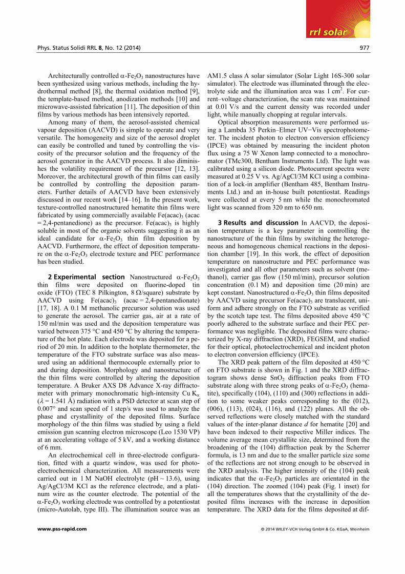
The XRD peak pattern of the film deposited at 450 °C on FTO substrate is shown in Fig. 1 and the XRD diffrac-togram shows dense SnO2 diffraction peaks from FTO substrate along with three strong peaks of α-Fe2O3 (hema-tite), specifically (104), (110) and (300) reflections in addi-tion to some weaker peaks corresponding to the (012), (006), (113), (024), (116), and (122) planes. All the ob-served reflections were closely matched with the standard values of the inter-planar distance d for hematite [20] and have been indexed to their respective Miller indices. The volume average mean crystallite size, determined from the broadening of the (104) diffraction peak by the Scherrer formula, is 13 nm and due to the smaller particle size some of the reflections are not strong enough to be observed in the XRD analysis. The higher intensity of the (104) peak indicates that the α-Fe2O3 particles are orientated in the (104) direction. The zoomed (104) peak (Fig. 1 inset) for all the temperatures shows that the crystallinity of the de-posited films increases with the increase in deposition temperature. The XRD data for the films deposited at dif-
978 A. A. Tahir et al.: Photoelectrochemical properties of texture-controlled α-Fe2O3 thin films
© 2014 WILEY-VCH Verlag GmbH & Co. KGaA, Weinheim www.pss-rapid.com
stat
us
solid
i
ph
ysic
a rrl
Figure 1 XRD pattern of α-Fe2O3 thin film deposited from pre-cursor Fe(acac)3 at 450 °C on an FTO substrate. The peaks mark-ed with (*) correspond to SnO2. Inset: The zoomed (104) peak for all temperatures. The XRD is normalized to the high intensity SnO2 peak at 37.9°.
ferent temperature is normalized to the high intensity SnO2 peak at 37.9°. Martínez et al. [21] reported the deposition of α-Fe2O3 films using Fe(β-diketonate) precursor and found that structural properties such as crystallinity and phase are strongly dependent on the deposition temperature. Similarly, Duret et al. deposited films from Fe(acac)3 using a slightly different process (ultrasonic spray pyrolysis) and found Fe3O4 phase along with α-Fe2O3 [22]. The analysis also proved that no other iron oxide phase is detected in the XRD data suggesting that the current method is better to prepare nanostructured α-Fe2O3 thin films using Fe(acac)3.
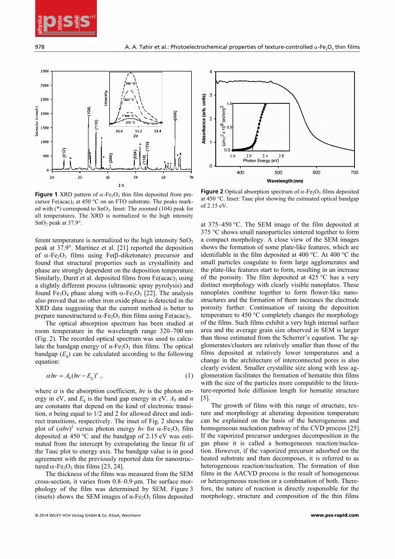
The optical absorption spectrum has been studied at room temperature in the wavelength range 320–700 nm (Fig. 2). The recorded optical spectrum was used to calcu-late the bandgap energy of α-Fe2O3 thin films. The optical bandgap (Eg) can be calculated according to the following equation:
0 g( ) ,nh A h E= -α ν ν (1)
where α is the absorption coefficient, hν is the photon en-ergy in eV, and Eg is the band gap energy in eV. A0 and n are constants that depend on the kind of electronic transi-tion, n being equal to 1/2 and 2 for allowed direct and indi-rect transitions, respectively. The inset of Fig. 2 shows the plot of (αhν)2 versus photon energy hν for α-Fe2O3 film deposited at 450 °C and the bandgap of 2.15 eV was esti-mated from the intercept by extrapolating the linear fit of the Tauc plot to energy axis. The bandgap value is in good agreement with the previously reported data for nanostruc-tured α-Fe2O3 thin films [23, 24].
The thickness of the films was measured from the SEM cross-section, it varies from 0.8–0.9 μm. The surface mor-phology of the film was determined by SEM. Figure 3 (insets) shows the SEM images of α-Fe2O3 films deposited
Figure 2 Optical absorption spectrum of α-Fe2O3 films deposited at 450 °C. Inset: Tauc plot showing the estimated optical bandgap of 2.15 eV.
at 375–450 °C. The SEM image of the film deposited at 375 °C shows small nanoparticles sintered together to form a compact morphology. A close view of the SEM images shows the formation of some plate-like features, which are identifiable in the film deposited at 400 °C. At 400 °C the small particles coagulate to form large agglomerates and the plate-like features start to form, resulting in an increase of the porosity. The film deposited at 425 °C has a very distinct morphology with clearly visible nanoplates. These nanoplates combine together to form flower-like nano- structures and the formation of them increases the electrode porosity further. Continuation of raising the deposition temperature to 450 °C completely changes the morphology of the films. Such films exhibit a very high internal surface area and the average grain size observed in SEM is larger than those estimated from the Scherrer’s equation. The ag-glomerates/clusters are relatively smaller than those of the films deposited at relatively lower temperatures and a change in the architecture of interconnected pores is also clearly evident. Smaller crystallite size along with less ag-glomeration facilitates the formation of hematite thin films with the size of the particles more compatible to the litera-ture-reported hole diffusion length for hematite structure [5].
The growth of films with this range of structure, tex-ture and morphology at alterating deposition temperature can be explained on the basis of the heterogeneous and homogeneous nucleation pathway of the CVD process [25]. If the vaporized precursor undergoes decomposition in the gas phase it is called a homogeneous reaction/nuclea- tion. However, if the vaporized precursor adsorbed on the heated substrate and then decomposes, it is referred to as heterogeneous reaction/nucleation. The formation of thin films in the AACVD process is the result of homogeneous or heterogeneous reaction or a combination of both. There-fore, the nature of reaction is directly responsible for the morphology, structure and composition of the thin films

Phys. Status Solidi RRL 8, No. 12 (2014) 979
www.pss-rapid.com © 2014 WILEY-VCH Verlag GmbH & Co. KGaA, Weinheim
[26]. By keeping all the other AACVD parameters constant, the type of nucleation reaction (homogeneous or heteroge-neous) can easily be controlled by the substrate tempera-ture. In the current work, this phenomenon was exploited to deposit α-Fe2O3 thin films with diverse texture and nanostructure by altering the deposition temperature. We attribute the change in morphology with the increase in temperature to the gradual shift of nucleation from hetero-geneous to homogeneous. The mechanism of AACVD deposition and the effect of homogeneous or heterogene-ous nucleation on the texture and morphology of thin films has been discussed in detail elsewhere [18, 27].
The photoelectrochemical performance of nanostruc-tured α-Fe2O3 films was studied by recording the photo-current density as a function of applied voltage (Fig. 3). The steady-state photocurrent density increased with the increase of deposition temperature. The photocurrent be-haviour has also been studied under chopped light and for comparison, the steady-state J–V plot was superimposed on the transient plot in each case. Steady-state and tran-sient J–V plots agree well for all electrodes. Generally, dark current starts at about 0.6 V for all the electrodes in 1 M NaOH electrolyte. The amount of dark current also decreased with the increase of deposition temperature. For all electrodes, the photocurrent increased rapidly with the applied potential. Figure 3 shows a maximum photocurrent of 455 μA cm−2 at 0.25 V for the electrode deposited at 450 °C. The photocurrent maximum observed for the elec-trode prepared at 450 °C can be interpreted in terms of a large active surface area (hence a large effective semicon-ductor/electrolyte interface), which possibly is associated with enhanced charge transfer at the interface. The separa-tion of photogenerated carriers within the width of the
space charge layer becomes a key factor, which seems to be more pronounced in the case of the electrode deposited at 450 °C. This increase can also be attributed to high crys-tallinity of the films as confirmed by the XRD analysis. The electrode prepared at 375 °C has the weakest PEC per-formance with recombination features in the photocurrent transient responses close to the photocurrent onset region, presumably due to its compact morphology. With the in-crease of deposition temperature, the electrode structure became more porous. The nanoporous structure (at 425 °C and 450 °C) has an advantage as it contains α-Fe2O3 nano- structures which provide a better electrode/electrolye inter-face for rapid charge transfer. Such nanostructures offer a very short distance required for the photogenerated holes to reach the electrolyte interface thereby suppressing the recombination. The PEC performance of films deposited at 450 °C is comparable to our previous α-Fe2O3 photoelec-trode deposited using a metal-organic complex [17]. This increases the rate of PEC water splitting by holes despite a hole diffusion length in the order of 2–4 nm [5]. Further work is needed to control the particle size of hematite nanostructures in the same order of hole-diffusion length to enhance the PEC performance.
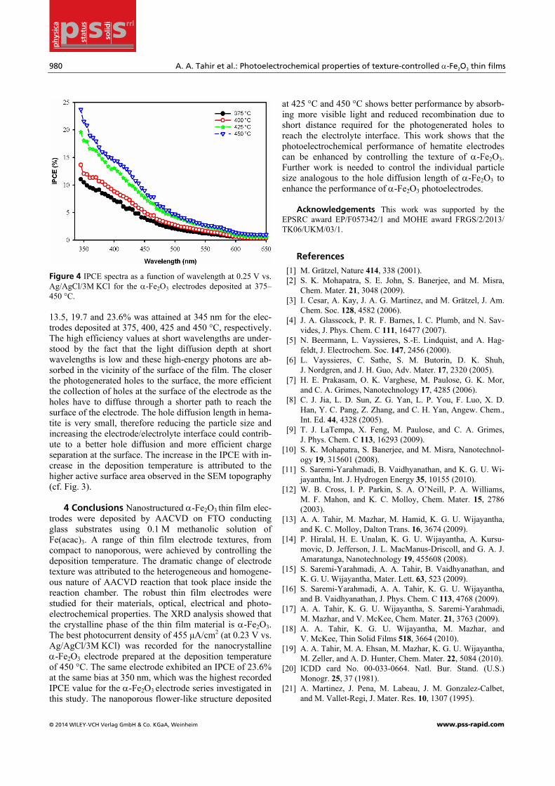
In order to further explore the influence of temperature on the PEC performance of the films deposited at different temperatures, the incident photon to electron conversion efficiency (IPCE) measurements were conducted at differ-ent wavelengths and at 0.25 V vs. Ag/AgCl/3M KCl. As shown in Fig. 4, the IPCE of the electrodes are almost similar at wavelengths greater than 610 nm which is out-side the absorption threshold of α-Fe2O3. The IPCE in-creases with increase in the deposition temperature after the absorption threshold. A maximum efficiency of 11.5,
Figure 3 J–V curves for α-Fe2O3electrodes deposited at different deposition temperatures. Insets:High-resolution SEM of the respec-tive electrodes.
980 A. A. Tahir et al.: Photoelectrochemical properties of texture-controlled α-Fe2O3 thin films
© 2014 WILEY-VCH Verlag GmbH & Co. KGaA, Weinheim www.pss-rapid.com
stat
us
solid
i
ph
ysic
a rrl
Figure 4 IPCE spectra as a function of wavelength at 0.25 V vs. Ag/AgCl/3M KCl for the α-Fe2O3 electrodes deposited at 375–450 °C.
13.5, 19.7 and 23.6% was attained at 345 nm for the elec-trodes deposited at 375, 400, 425 and 450 °C, respectively. The high efficiency values at short wavelengths are under-stood by the fact that the light diffusion depth at short wavelengths is low and these high-energy photons are ab-sorbed in the vicinity of the surface of the film. The closer the photogenerated holes to the surface, the more efficient the collection of holes at the surface of the electrode as the holes have to diffuse through a shorter path to reach the surface of the electrode. The hole diffusion length in hema-tite is very small, therefore reducing the particle size and increasing the electrode/electrolyte interface could contrib-ute to a better hole diffusion and more efficient charge separation at the surface. The increase in the IPCE with in-crease in the deposition temperature is attributed to the higher active surface area observed in the SEM topography (cf. Fig. 3).
4 Conclusions Nanostructured α-Fe2O3 thin film elec-
trodes were deposited by AACVD on FTO conducting glass substrates using 0.1 M methanolic solution of Fe(acac)3. A range of thin film electrode textures, from compact to nanoporous, were achieved by controlling the deposition temperature. The dramatic change of electrode texture was attributed to the heterogeneous and homogene-ous nature of AACVD reaction that took place inside the reaction chamber. The robust thin film electrodes were studied for their materials, optical, electrical and photo- electrochemical properties. The XRD analysis showed that the crystalline phase of the thin film material is α-Fe2O3. The best photocurrent density of 455 μA/cm2 (at 0.23 V vs. Ag/AgCl/3M KCl) was recorded for the nanocrystalline α-Fe2O3 electrode prepared at the deposition temperature of 450 °C. The same electrode exhibited an IPCE of 23.6% at the same bias at 350 nm, which was the highest recorded IPCE value for the α-Fe2O3 electrode series investigated in this study. The nanoporous flower-like structure deposited
at 425 °C and 450 °C shows better performance by absorb-ing more visible light and reduced recombination due to short distance required for the photogenerated holes to reach the electrolyte interface. This work shows that the photoelectrochemical performance of hematite electrodes can be enhanced by controlling the texture of α-Fe2O3. Further work is needed to control the individual particle size analogous to the hole diffusion length of α-Fe2O3 to enhance the performance of α-Fe2O3 photoelectrodes.
Acknowledgements This work was supported by the EPSRC award EP/F057342/1 and MOHE award FRGS/2/2013/ TK06/UKM/03/1.
References [1] M. Grätzel, Nature 414, 338 (2001). [2] S. K. Mohapatra, S. E. John, S. Banerjee, and M. Misra,
Chem. Mater. 21, 3048 (2009). [3] I. Cesar, A. Kay, J. A. G. Martinez, and M. Grätzel, J. Am.
Chem. Soc. 128, 4582 (2006). [4] J. A. Glasscock, P. R. F. Barnes, I. C. Plumb, and N. Sav-
vides, J. Phys. Chem. C 111, 16477 (2007). [5] N. Beermann, L. Vayssieres, S.-E. Lindquist, and A. Hag-
feldt, J. Electrochem. Soc. 147, 2456 (2000). [6] L. Vayssieres, C. Sathe, S. M. Butorin, D. K. Shuh,
J. Nordgren, and J. H. Guo, Adv. Mater. 17, 2320 (2005). [7] H. E. Prakasam, O. K. Varghese, M. Paulose, G. K. Mor,
and C. A. Grimes, Nanotechnology 17, 4285 (2006). [8] C. J. Jia, L. D. Sun, Z. G. Yan, L. P. You, F. Luo, X. D.
Han, Y. C. Pang, Z. Zhang, and C. H. Yan, Angew. Chem., Int. Ed. 44, 4328 (2005).
[9] T. J. LaTempa, X. Feng, M. Paulose, and C. A. Grimes, J. Phys. Chem. C 113, 16293 (2009).
[10] S. K. Mohapatra, S. Banerjee, and M. Misra, Nanotechnol-ogy 19, 315601 (2008).
[11] S. Saremi-Yarahmadi, B. Vaidhyanathan, and K. G. U. Wi-jayantha, Int. J. Hydrogen Energy 35, 10155 (2010).
[12] W. B. Cross, I. P. Parkin, S. A. O’Neill, P. A. Williams, M. F. Mahon, and K. C. Molloy, Chem. Mater. 15, 2786 (2003).
[13] A. A. Tahir, M. Mazhar, M. Hamid, K. G. U. Wijayantha, and K. C. Molloy, Dalton Trans. 16, 3674 (2009).
[14] P. Hiralal, H. E. Unalan, K. G. U. Wijayantha, A. Kursu-movic, D. Jefferson, J. L. MacManus-Driscoll, and G. A. J. Amaratunga, Nanotechnology 19, 455608 (2008).
[15] S. Saremi-Yarahmadi, A. A. Tahir, B. Vaidhyanathan, and K. G. U. Wijayantha, Mater. Lett. 63, 523 (2009).
[16] S. Saremi-Yarahmadi, A. A. Tahir, K. G. U. Wijayantha, and B. Vaidhyanathan, J. Phys. Chem. C 113, 4768 (2009).
[17] A. A. Tahir, K. G. U. Wijayantha, S. Saremi-Yarahmadi, M. Mazhar, and V. McKee, Chem. Mater. 21, 3763 (2009).
[18] A. A. Tahir, K. G. U. Wijayantha, M. Mazhar, and V. McKee, Thin Solid Films 518, 3664 (2010).
[19] A. A. Tahir, M. A. Ehsan, M. Mazhar, K. G. U. Wijayantha, M. Zeller, and A. D. Hunter, Chem. Mater. 22, 5084 (2010).
[20] ICDD card No. 00-033-0664. Natl. Bur. Stand. (U.S.) Monogr. 25, 37 (1981).
[21] A. Martinez, J. Pena, M. Labeau, J. M. Gonzalez-Calbet, and M. Vallet-Regi, J. Mater. Res. 10, 1307 (1995).

Phys. Status Solidi RRL 8, No. 12 (2014) 981
www.pss-rapid.com © 2014 WILEY-VCH Verlag GmbH & Co. KGaA, Weinheim
[22] A. Duret and M. Grätzel, J. Phys. Chem. B 109, 17184 (2005).
[23] J. D. Desai, H. M. Pathan, S.-K. Min, K.-D. Jung, and O.-S. Joo, Appl. Surf. Sci. 252, 8039 (2006).
[24] J. D. Desai, H. M. Pathan, S.-K. Min, K.-D. Jung, and O.-S. Joo, Semicond. Sci. Technol. 20, 705 (2005).
[25] X. Hou and K.-L. Choy, Chem. Vapor Depos. 12, 583 (2006).
[26] T. T. Kodas and M. J. Hampden-Smith, The Chemistry of Metal CVD (VCH, Weinheim, 1994).
[27] A. A. Tahir, H. A. Burch, K. G. U. Wijayantha, and B. G. Pollet, Int. J. Hydrogen Energy 38, 4315 (2013).