Intrahistoria de una rebelión contra la Intendencia. El motín de Ceballos de 1723
Upload
khangminh22Category
view
1download
0
PCI-172316-bit / 8-ch. Non-Isolated Analog Output Card
User Manual

CopyrightThe documentation and the software included with this product are copy-righted 2004 by Advantech Co., Ltd. All rights are reserved. Advantech Co., Ltd. reserves the right to make improvements in the products described in this manual at any time without notice. No part of this man-ual may be reproduced, copied, translated or transmitted in any form or by any means without the prior written permission of Advantech Co., Ltd. Information provided in this manual is intended to be accurate and reli-able. However, Advantech Co., Ltd. assumes no responsibility for its use, nor for any infringements of the rights of third parties, which may result from its use.
AcknowledgementsPC-LabCard is a trademark of Advantech Co., Ltd. IBM and PC are trademarks of International Business Machines Corporation. MS-DOS, Windows, Microsoft Visual C++ and Visual BASIC are trademarks of Microsoft Corporation. Intel and Pentium are trademarks of Intel Corpo-ration. Delphi and C++ Builder are trademarks of Inprise Corporation.All other product names or trademarks are properties of their respective owners.
Part No. 2003172300 1st EditionPrinted in Taiwan April 2004
PCI-1723 User Manual ii

Product Warranty (2 years)Advantech warrants to you, the original purchaser, that each of its prod-ucts will be free from defects in materials and workmanship for two years from the date of purchase. This warranty does not apply to any products which have been repaired or altered by persons other than repair personnel authorized by Advantech, or which have been subject to misuse, abuse, accident or improper instal-lation. Advantech assumes no liability under the terms of this warranty as a consequence of such events.Because of Advantech�s high quality-control standards and rigorous test-ing, most of our customers never need to use our repair service. If an Advantech product is defective, it will be repaired or replaced at no charge during the warranty period. For out-of-warranty repairs, you will be billed according to the cost of replacement materials, service time and freight. Please consult your dealer for more details.
If you think you have a defective product, follow these steps:1. Collect all the information about the problem encountered. (For
example, CPU speed, Advantech products used, other hardware and software used, etc.) Note anything abnormal and list any onscreen messages you get when the problem occurs.
2. Call your dealer and describe the problem. Please have your man-ual, product, and any helpful information readily available.
3. If your product is diagnosed as defective, obtain an RMA (return merchandize authorization) number from your dealer. This allows us to process your return more quickly.
4. Carefully pack the defective product, a fully-completed Repair and Replacement Order Card and a photocopy proof of purchase date (such as your sales receipt) in a shippable container. A product returned without proof of the purchase date is not eligible for war-ranty service.
5. Write the RMA number visibly on the outside of the package and ship it prepaid to your dealer.
iii
CEThis product has passed the CE test for environmental specifications when shielded cables are used for external wiring. We recommend the use of shielded cables. This kind of cable is available from Advantech. Please contact your local supplier for ordering information.
Packing ListBefore setting up the system, check that the items listed below are included and in good condition. If any item does not accord with the table, please contact your dealer immediately.Before you install your PCI-1723 card, please make sure you have the following necessary components:� PCI-1723 DA&C card� PCI-1723 User�s Manual� Advantech DLL drivers (Included in the companion CD-ROM)� Wiring cable PCL-10168 (option)� Wiring board ADAM-3968 (option)� Personal computer or workstation with a PCI-bus slot (running Win-
dows 2000/95/ 98/NT/ME/XP)
PCI-1723 User Manual iv

ContentsChapter 1 Introduction ..................................................... 2
1.1 Features ............................................................................. 21.2 Applications ...................................................................... 31.3 Installation Guide .............................................................. 4
Figure 1.1:Installation Flow Chart ................................. 51.4 Software Overview............................................................ 61.5 Device Driver Programming Roadmap ............................ 71.6 Accessories........................................................................ 8
Chapter 2 Installation ..................................................... 122.1 Unpacking ....................................................................... 122.2 Driver Installation ........................................................... 13
Figure 2.1:Advantech Automation Software Setup ..... 13Figure 2.2:Different Options for Driver Setup ............ 14
2.3 Hardware Installation ...................................................... 15Figure 2.3:Device Name on the Device Manager ........ 16
2.4 Device Setup and Configuration .................................... 172.4.1 Setting Up the Device .................................................. 17
Figure 2.4:The Device Manager Dialog Box ............... 17Figure 2.5:�Device(s) Found� Dialog Box .................. 18
2.4.2 Configuring the Device ................................................ 18Figure 2.6:The Device Setting dialog box ................... 18Figure 2.7:Device Name on List of Devices Box ........ 19
Chapter 3 Signal Connections ........................................ 223.1 Overview ......................................................................... 223.2 Switch and Jumper Settings ............................................ 22
Figure 3.1:Connector, Jumper & Switch Locations .... 223.2.1 JP9 ................................................................................ 233.2.2 JP1~JP8 ........................................................................ 233.2.3 Setting the Time to Reset Analog Outputs .................. 233.2.4 Board ID setting ........................................................... 24
3.3 Signal Connections ......................................................... 253.3.1 Pin Assignment ............................................................ 25
Figure 3.2:I/O Connector Pin Assignments ................. 253.3.2 I/O Connector Signal Descriptions .............................. 26
Table 3.1:I/O Connector Signal Descriptions .............. 263.3.3 Analog Output Connection .......................................... 26
Figure 3.3:Analog Output Connections ....................... 273.4 Field Wiring Considerations ........................................... 28
Appendix A Specifications ................................................. 30A.1 Analog Output ................................................................. 30A.2 Digital Input /Output ....................................................... 30A.3 General ........................................................................... 31
v Table of Contents

Appendix B Block Diagram............................................... 34Appendix C Register Structure & Format....................... 36
C.1 Overview ......................................................................... 36C.2 I/O Port Address Map ..................................................... 36
Table C.1:PCI-1723 Register Format .......................... 37Table C.2:PCI-1723 register format (Part 2) ............... 39
C.3 D/A channels output data � BASE+00H~0EH ............ 41Table C.3:Register for D/A Channels Output Data ..... 41
C.4 D/A channels latch data � BASE+00H~0EH................ 42Table C.4:Register for D/A Channels Latch Data ....... 42
C.5 Board ID � BASE+10H ................................................ 43Table C.5:Register for Board ID .................................. 43
C.6 D/A Channels Synchronized Settings (BASE+12H) ...... 44Table C.6:D/A channels synchronous setting .............. 44
C.7 All D/A Channels Synchronized Status � BASE+12H. 45Table C.7:D/A Channels Synchronized Status ............ 45
C.8 DAC Range and Calibration Mode � BASE+14H........ 45Table C.8:DAC Range and Calibration Mode ............. 45
C.9 DAC Range and Calibration Status � BASE+14H ....... 46Table C.9:DAC range and calibration status ............... 46
C.10 SADC Control Command for Calibration Function� BASE+16H48
Table C.10:SADC control command for calibration ... 48C.11 SADC Control Status for Calibration Function� BASE+16H48
Table C.11:SADC control for calibration .................... 48C.12 Calibration Parameter Strobe � BASE+18H................. 49
Table C.12:Calibration parameter strobe ..................... 49C.13 Digital I/O setting � BASE+1AH ................................ 49
Table C.13:Register for digital I/O port setting ........... 49C.14 Digital I/O port mode � BASE+1AH............................ 50
Table C.14:Register for digital I/O port modes ........... 50C.15 Write Digital Output Command � BASE+1CH............ 50
Table C.15:Register for write digital output command 50C.16 Read Digital Input Data � BASE+1CH ........................ 51
Table C.16:Register for Read Digital Input Data ........ 51C.17 Write Calibration Command � BASE+1EH ................. 51
Table C.17:Register for write calibration command ... 51C.18 Read calibration status � BASE+1EH........................... 52
Table C.18: Register for read calibration status .......... 52Table C.19:Register for synchronized strobe .............. 52
C.19 Reset all D/A channels strobe � BASE+22H................ 53Table C.20:Register for reset all D/A channels strobe 53
C.20 Reset the calibration controller strobe � BASE+24H ... 53Table C.21:Reset the calibration controller strobe ...... 53
C.21 Change D/A channels output strobe (BASE+26H)......... 53Table C.22:Change D/A channels output type strobe .. 53
C.22 Select the calibration Ref_V � BASE+28H .................. 54Table C.23:Register for select the calibration Ref_V .. 54
C.23 Summary ......................................................................... 54
MIC-3780 User Manual vi

2
CH
AP
TE
R 1Introduction
This chapter gives background informa-tion on the PCI-1723. Sections include:
� Features� Applications� Installation Guide� Software Overview� Device Driver Programming Roadmap� Accessories

Chapter 1 IntroductionThank you for buying the Advantech PCI-1723. The PCI-1723 is a non-isolated multiple channels analog output card for PCI bus, and each ana-log output channel is equipped with a 16-bit, double-buffered DAC. It features an auto-calibration function and Board ID. The PCI-1723 is an ideal solution for industrial applications where multi-ple analog output channels are required.The following sections of this chapter will provide further information about features of the multifunction cards, a Quick Start for installation, together with some brief information on software and accessories for the PCI-1723 card.
1.1 Features
� Auto calibration function� A 16-bit DAC is equipped for each of the analog output channels� Flexible output range: ±10 V, 0 ~ 20 mA, 4 ~ 20 mA� Synchronized output function� Output values kept after system hot reset� 2-port (16-channel) user-defined digital input/output� Board ID
The Advantech PCI-1723 offers the following main features:
Auto-Calibration FunctionThe PCI-1723 provides an auto-calibration function by using a calibra-tion utility. The built-in calibration circuitry of the PCI-1723 corrects gain and offset errors in analog output channels, thereby eliminating the need for external equipment and user adjustments.
PCI-1723 User Manual 2

Flexible Voltage Output RangeThe PCI-1723 provides a fixed voltage output range of °�10 V to fulfill your flexible range needed applications. Users can define the specific voltage output range and output data format via the enclosed software utility and driver.
Keeping Output Values After System ResetUsers can independently set the eight outputs to different ranges: °�10 V, 0 ~ 20 mA or 4 ~ 20 mA, and all ranges are software selectable. When the system is hot reset (power not shut down), the PCI-1723 can either retain the last analog output values, or return to its default configuration, depending on the jumper setting. This practical function eliminates dan-ger caused by improper operation during unexpected system reset.
Board IDThe PCI-1723 has a built-in DIP Switch that helps define each card�s ID when multiple PCI-1723 cards have been installed on the same PC chas-sis. The board ID setting function is very useful when users build their system with multiple PCI-1723 cards. With correct Board ID settings, you can easily identify and access each card during hardware configura-tion and software programming.
1.2 Applications
� Process control� Programmable voltage source� Programmable current sink� Servo control� Multiple loop PID control
Note: For detailed specifications of the PCI-1723, please refer to Appendix A, Specifications.
3 Chapter 1

1.3 Installation Guide
Before you install your PCI-1723 card, please make sure you have the following necessary components:
� PCI-1723 DA&C card� PCI-1723 User�s Manual� Advantech DLL drivers (Included in the companion CD-ROM)� Wiring cable PCL-10168 (option)� Wiring board ADAM-3968 (option)� Personal computer or workstation with a PCI-bus slot (running Win-
dows 2000/95/ 98/NT/ME/XP)
Some other optional components are also available for enhanced opera-tion such as application software ActiveDAQ, GeniDAQ and other third-party software packages
After you get the necessary components and maybe some of the accesso-ries for enhanced operation of your Multifunction card, you can then begin the installation procedure. Figure 1-1 on the next page provides a concise flow chart to give users a broad picture of the software and hard-ware installation procedures:
PCI-1723 User Manual 4

Figure 1.1: Installation Flow Chart
5 Chapter 1

1.4 Software Overview
Advantech offers a rich set of DLL drivers, third-party driver support and application software to help fully exploit the functions of your PCI-1723 card:
� Device Drivers (on the companion CD-ROM)� LabVIEW driver� Advantech ActiveDAQ� Advantech GeniDAQ
Programming choices for DA&C cards: You may use Advantech applica-tion software such as Advantech Device Drivers. On the other hand, advanced users are allowed another option for register-level program-ming, although not recommended due to its laborious and time-consum-ing nature.
Device DriversThe Advantech Device Drivers software is included on the companion CD-ROM at no extra charge. It also comes with all the Advantech DA&C cards. Advantech�s Device Drivers features a complete I/O function library to help boost your application performance. The Advantech Device Drivers for Windows 2000/95/98/NT/ME/XP works seamlessly with development tools such as Visual C++, Visual Basic, Inprise C++ Builder and Inprise Delphi.
Register-Level ProgrammingRegister-level programming is available for experienced programmers who find it necessary to write code directly at the level of the device reg-ister. Since register-level programming requires much effort and time, we recommend that you use the Advantech Device Drivers instead. How-ever, if register-level programming is indispensable, you should refer to the relevant information in Appendix C, Register Structure and Format, or to the example codes included on the companion CD-ROM.
PCI-1723 User Manual 6

1.5 Device Driver Programming Roadmap
This section will provide you a roadmap to demonstrate how to build an application from scratch using Advantech Device Drivers with your favorite development tools such as Visual C++, Visual Basic, Delphi and C++ Builder. The step-by-step instructions on how to build your own applications using each development tool will be given in the Device Drivers Manual. Moreover, a rich set of example source code is also given for your reference.
Programming ToolsProgrammers can develop application programs with their favorite devel-opment tools:� Visual C++� Visual Basic� Delphi� C++ BuilderFor instructions on how to begin programming works in each develop-ment tool, Advantech offers a Tutorial Chapter in the Device Drivers Manual for your reference. Please refer to the corresponding sections in this chapter on the Device Drivers Manual to begin your programming efforts. You can also look at the example source code provided for each programming tool, since they can get you very well oriented.
The Device Drivers Manual can be found on the companion CD-ROM. Alternatively, if you have already installed the Device Drivers on your system, The Device Drivers Manual can be readily accessed through the Start button:Start/Programs/Advantech Device Driver V2.0/Device Driver ManualThe example source code can be found under the corresponding installa-tion folder such as the default installation path:\Program Files\Advantech\ADSAPI\ExamplesFor information about using other function groups or other development tools, please refer to the Creating Windows 95/NT/2000 Application withDevice Drivers chapter and the Function Overview chapter on the Device Drivers Manual.
7 Chapter 1

Programming with Device Drivers Function LibraryAdvantech Device Drivers offer a rich function library that can be utilized in various application programs. This function library consists of numer-ous APIs that support many development tools, such as Visual C++, Visual Basic, Delphi and C++ Builder. According to their specific functions or services, the APIs can be catego-rized into several function groups:� Analog Output Function Group� Digital Input/Output Function Group� Counter Function Group� Port Function Group (direct I/O)� Event Function GroupFor the usage and parameters of each function, please refer to the Func-tion Overview chapter in the Device Drivers Manual.
Troubleshooting Device Drivers ErrorDriver functions will return a status code when they are called to perform a certain task for the application. When a function returns a code that is not zero, it means the function has failed to perform its designated func-tion. To troubleshoot the Device Drivers error, you can pass the error code to DRV_GetErrorMessage function to return the error message. Alternatively, you can refer to the Device Drivers Error Codes Appendix in the Device Drivers Manual for a detailed listing of Error Codes, Error IDs and the Error Messages.
1.6 Accessories
Advantech offers a complete set of accessory products to support the PCI-1723 card. These accessories include:Wiring Cable PCL-10168The PCL-10168 shielded cable is specially designed for PCI-1723 cards to provide high resistance to noise. To achieve a better signal quality, the signal wires are twisted in such a way as to form a �twisted-pair cable,� reducing cross talk and noise from other signal sources. Furthermore, its analog and digital lines are separately sheathed and shielded to neutralize EMI/EMC problems.
PCI-1723 User Manual 8

Wiring Board ADAM-3968The ADAM-3968 is a 68-pin SCSI wiring terminal module for DIN-rail mounting. This terminal module can be readily connected to the Advan-tech PC-Lab cards and allow easy yet reliable access to individual pin connections for the PCI-1723 card.
9 Chapter 1

PCI-1723 User Manual 10

2
CH
AP
TE
R 2Installation
This chapter gives users a package item checklist, proper instructions for unpacking and step-by-step procedures for both driver and card installation. Sections include:
� Unpacking� Driver Installation� Hardware Installation� Device Setup and Configuration

Chapter 2 Installation2.1 Unpacking
After receiving your PCI-1723 package, please inspect its contents first. The package should contain the following items:� PCI-1723 card� Companion CD-ROM (Device Drivers included)� User Manual
The PCI-1723 card harbors certain electronic components vulnerable to electrostatic discharge (ESD). ESD can easily damage the integrated cir-cuits and certain components if preventive measures are ignored.Before removing the card from the antistatic plastic bag, you should take the following precautions to ward off possible ESD damage:� Touch the metal part of your computer chassis with your hand to dis-
charge the static electricity accumulated on your body. Alternatively, one can also use a grounding strap.
� Touch the anti-static bag to a metal part of your computer chassis before opening the bag.
� Take hold of the card only by the metal bracket when removing it out of the bag.
After taking out the card, you should first:� Inspect the card for any possible signs of external damage (loose or
damaged components, etc.). If the card is visibly damaged, please notify our service department or our local sales representative immedi-ately. Do not install a damaged card into your system.
Also, pay extra caution to the following aspects to ensure proper installa-tion:� Avoid physical contact with materials that could hold static electricity
such as plastic, vinyl and Styrofoam.
PCI-1723 User Manual 12
� Whenever you handle the card, grasp it only by its edges. DO NOT TOUCH the exposed metal pins of the connector or the electronic com-ponents.
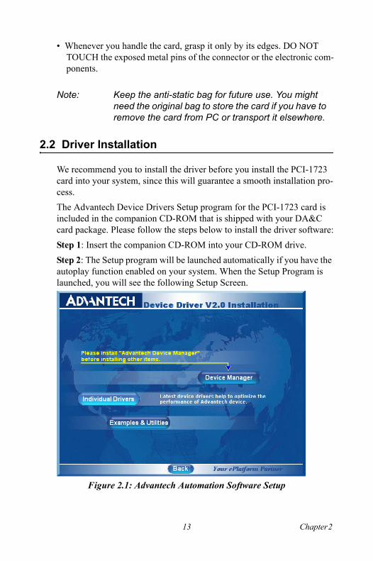
2.2 Driver Installation
We recommend you to install the driver before you install the PCI-1723 card into your system, since this will guarantee a smooth installation pro-cess.The Advantech Device Drivers Setup program for the PCI-1723 card is included in the companion CD-ROM that is shipped with your DA&C card package. Please follow the steps below to install the driver software:Step 1: Insert the companion CD-ROM into your CD-ROM drive.Step 2: The Setup program will be launched automatically if you have the autoplay function enabled on your system. When the Setup Program is launched, you will see the following Setup Screen.
Figure 2.1: Advantech Automation Software Setup
Note: Keep the anti-static bag for future use. You might need the original bag to store the card if you have to remove the card from PC or transport it elsewhere.
13 Chapter 2

Step 3: Select the Device Drivers option.Step 4: Select the specific device then just follow the installation instruc-tions step by step to complete your device driver installation and setup.
Figure 2.2: Different Options for Driver SetupFor further information on driver-related issues, an online version of the Device Drivers Manual is available by accessing the following path: Start/Programs/Advantech Device Drivers V2.0/Device Drivers Manual
Note: If the autoplay function is not enabled on your com-puter, use Windows Explorer or Windows Run com-mand to execute SETUP.EXE on the companion CD-ROM.
PCI-1723 User Manual 14

2.3 Hardware Installation
Make sure you have installed the driver first before you install the card (please refer to 2.2 Driver Installation).
After the Device Drivers installation is completed, you can then install the PCI-1723 card into any PCI slot on your computer. However, it is suggested that you refer to the computer user�s manual or related docu-mentation if you have any doubt. Please follow the steps below to install the card onto your system. 1. Turn off your computer and unplug the power cord and cables.
TURN OFF your computer before installing or removing any com-ponents on the computer.
2. Remove the cover of your computer.3. Remove the slot cover on the back panel of your computer.4. Touch the metal part on the surface of your computer to neutralize
the static electricity that might be on your body.5. Insert the PCI-1723 card into a PCI slot. Hold the card only by its
edges and carefully align it with the slot. Insert the card firmly into place. Use of excessive force must be avoided; otherwise, the card might be damaged.
6. Fasten the bracket of the PCI card on the back panel rail of the computer with screws.
7. Connect appropriate accessories (68-pin cable, wiring terminals, etc. if necessary) to the PCI card.
8. Replace the cover of your computer chassis. Re-connect the cables you removed in step 2.
9. Plug in the power cord and turn on the computer.
Note: In case you installed the card without installing the Device Drivers first, Windows 95/98/ME will recog-nize your card as an �unknown device� after rebooting, and will prompt you to provide the nec-essary driver. You should ignore the prompting messages (just click the Cancel button) and set up the driver according to the steps described in 2.2 Driver Installation.
15 Chapter 2

After the PCI-1723 card is installed, you can verify whether it is properly installed on your system in the Device Manager:1. Access the Device Manager through Control Panel/System/Device
Manager.2. The device name of the PCI-1723 should be listed on the Device
Manager tab on the System Property Page.
Figure 2.3: Device Name on the Device Manager
If your card is properly installed, you should see the device name of your card listed on the Device Manager tab. If you do see your device name listed on it but marked with an exclamation sign �!�, it means your card has not been correctly installed. In this case, remove the card device from the Device Manager by selecting its device name and press the Remove button. Then go through the driver installation process again.
After your card is properly installed on your system, you can now config-ure your device using the Advantech Device Manager Program that has itself already been installed on your system during driver setup. A com-plete device installation procedure should include device setup, configu-ration and testing. The following sections will guide you through the Setup, Configuration and Testing of your device.
PCI-1723 User Manual 16

2.4 Device Setup and Configuration
The Advantech Device Manager program is a utility that allows you to set up, configure and test your device, and later stores your settings on the system registry. These settings will be used when you call the APIs of Advantech Device Drivers.
2.4.1 Setting Up the Device1. To install the I/O device for your card, you must first run the
Device Installation program (by accessing Start/Programs/ Advan-tech Device Driver V2.0).
2. You can then view the device(s) already installed on your system (if any) on the Installed Devices list box. Since you have not installed any device yet, you might see a blank list such as the one below (Fig. 2-4).
Figure 2.4: The Device Manager Dialog Box
17 Chapter 2

3. Scroll down the List of Devices box to find the device that you wish to install, then click the Add� button to evoke the Device(s) found dialog box such as one shown in Fig. 2-5. The Device(s) found dialog box lists all the installed devices on your system. Select the device you want to configure from the list box and press the OK button. After you have clicked OK, you will see a Device Setting dialog box such as the one in Fig. 2-6.
Figure 2.5: �Device(s) Found� Dialog Box
2.4.2 Configuring the Device4. On the Device Setting dialog box (Fig. 2-6), you can configure the
voltage output range for the 8 D/A channels.
Figure 2.6: The Device Setting dialog box
PCI-1723 User Manual 18

5. After you have finished configuring the device, click OK and the device name will appear in the Installed Devices box as seen below:
Figure 2.7: Device Name on List of Devices Box
After your card is properly installed and configured, you can click the Test� button to test your hardware by using the testing utility supplied. For more detailed information, please refer to Chapter 2 of the Device Drivers Manual.You can also find the rich examples on the CD-ROM to speed up your programming.
Note: As we have noted, the device name �000:PCI-1723 BoardID=0 I/O=6500H� begins with a device number �000�, which is specifically assigned to each card. The device number is passed to the driver to specify which device you wish to control.
19 Chapter 2

PCI-1723 User Manual 20

2
CH
AP
TE
R 3

Chapter 3 Signal Connections3.1 Overview
Maintaining signal connections is one of the most important factors in ensuring that your application system is sending and receiving data cor-rectly. A good signal connection can avoid unnecessary and costly dam-age to your PC and other hardware devices. This chapter provides useful information about how to connect input and output signals to the PCI-1723 via the I/O connector.
3.2 Switch and Jumper Settings
The PCI-1723 card has one function switch and five jumper settings
Figure 3.1: Connector, Jumper & Switch Locations
PCI-1723 User Manual 22

3.2.1 JP9
3.2.2 JP1~JP8
3.2.3 Setting the Time to Reset Analog OutputsSome users will want the capability of clearing each analog output when the system (or PC) issues a reset signal on the PCI bus. Some users will want to clear their analog output only as part of system power-on. The PCI-1723 satisfies both these needs by providing jumper JP1. Depending on the application, this capability may allow analog outputs to be "ZERO" without requiring a complete shutdown of processes con-trolled by the card.
Complete loss of power to the chip clears the chip memory. Thus, no mat-ter how JP1 is set, if the power to the PCI-1723 is disconnected, the ana-log output initial power-on state will be "ZERO".
Keep last status after hot reset.
Default configuration.
4~20 mA
0~20 mA
23 Chapter 3

3.2.4 Board ID setting
Note: On: 1, Off: 0
ID3 ID2 ID1 ID0 Board ID
1 1 1 1 0
1 1 1 0 1
1 1 0 1 2
1 1 0 0 3
1 0 1 1 4
1 0 1 0 5
1 0 0 1 6
1 0 0 0 7
0 1 1 1 8
0 1 1 0 9
0 1 0 1 10
0 1 0 0 11
0 0 1 1 12
0 0 1 0 13
0 0 0 1 14
0 0 0 0 15
PCI-1723 User Manual 24

3.3 Signal Connections
3.3.1 Pin AssignmentFigure 3-3 shows the pin assignments for the 68-pin I/O connector on the PCI-1723.
Figure 3.2: I/O Connector Pin Assignments
NC 68 34 NCVout0 67 33 Vout1AGND 66 32 AGNDIout0 65 31 Iout1NC 64 30 NCAGND 63 29 AGNDVout2 62 28 Vout3AGND 61 27 AGNDIout2 60 26 Iout3NC 59 25 NCAGND 58 24 AGNDVout4 57 23 Vout5AGND 56 22 AGNDIout4 55 21 Iout5NC 54 20 NCAGND 53 19 AGNDVout6 52 18 Vout7AGND 51 17 AGNDIout6 50 16 Iout7NC 49 15 NCAGND 48 14 AGNDDIO0 47 13 DIO1DIO2 46 12 DIO3DIO4 45 11 DIO5DIO6 44 10 DIO7DIO8 43 9 DIO9DIO10 42 8 DIO11DIO12 41 7 DIO13DIO14 40 6 DIO15DGND 39 5 DGNDNC 38 4 NCNC 37 3 NCNC 36 2 NC+12V 35 1 +5V
25 Chapter 3

3.3.2 I/O Connector Signal Descriptions
3.3.3 Analog Output ConnectionThe PCI-1723 provides eight D/A output channels, Vout_0 ~ Vout_7 and Iout_0 ~ Iout_7. Users may use the PCI-1723 internally provided preci-sion -5V (-10 V) reference to generate 0 to +5 V (+10 V) D/A output range.
The maximum driving ability for each channel is 2 mA when voltage mode is chosen. Please note that external resistor load can not be lower than | Vout | / 2 mA, or the card could be damaged.
Figure 3-3 shows how to make analog connections on the PCI-1723.
Table 3.1: I/O Connector Signal DescriptionsSignal Name
Refer-ence
Direc-tion
Description
Vout<0..3> AGND Output Voltage Output, Channels 0 through 3.
Iout<0..3> AGND Output Current Output, Channels 0 through 3.
AGND - - Analog Ground. The two ground refer-ences (AGND and DGND) are con-nected together on the PCI-1723 card.
DI0<0..15> DGND - Digital Input / Output signals. These pins are digital input / Output channel 0 to 15.
DGND - - Digital Ground. The two ground refer-ences (AGND and DGND) are con-nected together on the PCI-1723 card.
+12V DGND Output +12 VDC Source (from PCI bus directly with FUSE protection).
+5V DGND Output +5 VDC Source (from PCI bus directly with FUSE protection).
PCI-1723 User Manual 26

Figure 3.3: Analog Output Connections
Current output mode: Caution: The external voltage should be under 30 V.Ri: Internal resistor= 249 ohmVext: External voltageIsink : The controlled current output (0~20 mA)Since Isink =Vext / (Ri+RL), RL can not be higher than | Vext/Imax | -RiFor Example: Vext=24 V, Imax=20 mARL max = | 24 V / 20 mA | - 249= 951 (ohm)
n: 0 ~ 7
D/A nData Bus
Load
Vext
Isink_n
AGND
Ri
+
-
RL
Internal External
27 Chapter 3

PCI-1723 User Manual 28
3.4 Field Wiring Considerations
When you use the PCI-1723 to acquire data from outside, noises in the environment might significantly affect the accuracy of your measure-ments if due cautions are not taken. The following measures will be help-ful to reduce possible interference running signal wires between signal sources and the PCI-1723.
The signal cables must be kept away from strong electromagnetic sources such as power lines, large electric motors, circuit breakers or welding machines, since they may cause strong electromagnetic interference. Keep the analog signal cables away from any video monitor, since it can significantly affect a data acquisition system.
If the cable travels through an area with significant electromagnetic inter-ference, you should adopt individually shielded, twisted-pair wires as the analog input cable. This type of cable has its signal wires twisted together and shielded with a metal mesh. The metal mesh should only be con-nected to one point at the signal source ground.
Avoid running the signal cables through any conduit that might have power lines in it.
If you have to place your signal cable parallel to a power line that has a high voltage or high current running through it, try to keep a safe distance between them. Alternatively, you can place the signal cable at a right angle to the power line to minimize the undesirable effect.
The signals transmitted on the cable will be directly affected by the qual-ity of the cable. In order to ensure better signal quality, we recommend that you use the PCL-10168 shielded cable.

2
AP
PE
ND
IX ASpecifications
This appendix provides information on the specifications of PCI-1723.Sections include:
� Analog Output� Digital Input/Output� General

Appendix A SpecificationsA.1 Analog Output
A.2 Digital Input /Output
Channels 8
Resolution 16-bit
Operation mode Single output, Synchronized output
Output Range (Internal Reference only)
-10 ~+10 V, 0 ~ 20 mA, 4 ~ 20 mA
Accuracy Relative ±6 LSB
DifferentialNon-linear-ity
±6 LSB (monotonic)
Offset < 6 LSB
Output Impedance 0.1 max.
Throughput PC dependent, Software update (direct AO)
Settling time 50 us (to °�6 LSB of FSR)
Input Channels 16 (bi-directional)
Number of ports 2
Input Voltage Low 0.8 V max.
High 2.0 V min.
Output Voltage Low 0.5 V max. @ +24 mA (sink)
High 2.0 V min. @ -15 mA (source)
PCI-1723 User Manual 30

A.3 General
I/O Connector Type 68-pin SCSI-II female
Dimensions 175 x 100 mm (6.9" x 3.9")
Power Consumption
Typical +5 V @ 850 mA, +12 V @ 600 mA
Max. +5 V @ 1 A, +12 V @ 700 mA
Temperature Operation 0 ~ 60° C (32 ~158° F) (refer to IEC 68-2-1,2)
Storage -20~85° C (-4~185° F)
Relative Humidity 5~95% RH non-condensing (refer to IEC 68-2-3)
Certifications CE certified
31 Appendix A

PCI-1723 User Manual 32

2
AP
PE
ND
IX BBlock Diagram
This appendix shows the block diagram for PCI-1723.

PCI-1723 User Manual 34
Appendix B Block Diagram
Loc
al B
us
16-BitDAC 0
BidirectionalAnd Latched 8
Bits DIO
Auto Calibration Circuit
DIO[7:0]
Iout 0
Vout 0
16-BitDAC 1
Iout 1
Vout 1
16-BitDAC 2
Iout 2
Vout 2
16-BitDAC 3
Iout 3
Vout 3
PCI Interface
DIO[15:8]
PC
I B
us
BidirectionalAnd Latched 8
Bits DIO
16-BitDAC 4
Iout 4
Vout 4
16-BitDAC 5
Iout 5
Vout 5
16-BitDAC 6
Iout 6
Vout 6
16-BitDAC 7
Iout 7
Vout 7

2
AP
PE
ND
IX CRegister Structure & Format

Appendix C Register Structure & FormatC.1 Overview
The PCI-1723 is delivered with an easy-to-use 32-bit Device Drivers for user programming under the Windows 2000/95/98/NT/ME/XP operating system. We advise users to program the PCI-1723 using the 32-bit Device Drivers provided by Advantech to avoid the complexity of low-level reg-istry programming.
The most important consideration in programming the PCI-1723 the reg-ister level is to understand the function of the card's registers. The infor-mation in the following sections is provided only for users who would like to do their own low-level programming.
C.2 I/O Port Address Map
The PCI-1723 requires 32 consecutive addresses in the PC's I/O space. The address of each register is specified as an offset from the card's base address. For example, BASE+0 is the card's base address and BASE+7 is the base address plus seven bytes.
Table C-1 shows the function of each register of the PCI-1723 or driver and its address relative to the card's base address.
PCI-1723 User Manual 36
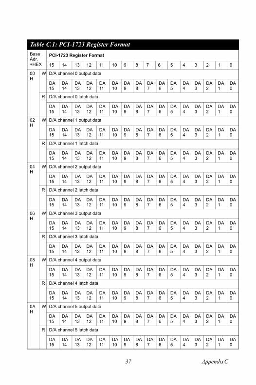
Table C.1: PCI-1723 Register FormatBaseAdr.+HEX
PCI-1723 Register Format
15 14 13 12 11 10 9 8 7 6 5 4 3 2 1 0
00H
W D/A channel 0 output data
DA15
DA14
DA13
DA12
DA11
DA10
DA9
DA8
DA7
DA6
DA5
DA4
DA3
DA2
DA1
DA0
R D/A channel 0 latch data
DA15
DA14
DA13
DA12
DA11
DA10
DA9
DA8
DA7
DA6
DA5
DA4
DA3
DA2
DA1
DA0
02H
W D/A channel 1 output data
DA15
DA14
DA13
DA12
DA11
DA10
DA9
DA8
DA7
DA6
DA5
DA4
DA3
DA2
DA1
DA0
R D/A channel 1 latch data
DA15
DA14
DA13
DA12
DA11
DA10
DA9
DA8
DA7
DA6
DA5
DA4
DA3
DA2
DA1
DA0
04H
W D/A channel 2 output data
DA15
DA14
DA13
DA12
DA11
DA10
DA9
DA8
DA7
DA6
DA5
DA4
DA3
DA2
DA1
DA0
R D/A channel 2 latch data
DA15
DA14
DA13
DA12
DA11
DA10
DA9
DA8
DA7
DA6
DA5
DA4
DA3
DA2
DA1
DA0
06H
W D/A channel 3 output data
DA15
DA14
DA13
DA12
DA11
DA10
DA9
DA8
DA7
DA6
DA5
DA4
DA3
DA2
DA1
DA0
R D/A channel 3 latch data
DA15
DA14
DA13
DA12
DA11
DA10
DA9
DA8
DA7
DA6
DA5
DA4
DA3
DA2
DA1
DA0
08H
W D/A channel 4 output data
DA15
DA14
DA13
DA12
DA11
DA10
DA9
DA8
DA7
DA6
DA5
DA4
DA3
DA2
DA1
DA0
R D/A channel 4 latch data
DA15
DA14
DA13
DA12
DA11
DA10
DA9
DA8
DA7
DA6
DA5
DA4
DA3
DA2
DA1
DA0
0AH
W D/A channel 5 output data
DA15
DA14
DA13
DA12
DA11
DA10
DA9
DA8
DA7
DA6
DA5
DA4
DA3
DA2
DA1
DA0
R D/A channel 5 latch data
DA15
DA14
DA13
DA12
DA11
DA10
DA9
DA8
DA7
DA6
DA5
DA4
DA3
DA2
DA1
DA0
37 Appendix C

0CH
W D/A channel 6 output data
DA15
DA14
DA13
DA12
DA11
DA10
DA9
DA8
DA7
DA6
DA5
DA4
DA3
DA2
DA1
DA0
R D/A channel 6 latch data
DA15
DA14
DA13
DA12
DA11
DA10
DA9
DA8
DA7
DA6
DA5
DA4
DA3
DA2
DA1
DA0
0EH
W D/A channel 7 output data
DA15
DA14
DA13
DA12
DA11
DA10
DA9
DA8
DA7
DA6
DA5
DA4
DA3
DA2
DA1
DA0
R D/A channel 7 latch data
DA15
DA14
DA13
DA12
DA11
DA10
DA9
DA8
DA7
DA6
DA5
DA4
DA3
DA2
DA1
DA0
10H
W N/A
R Board ID
0 0 0 0 0 0 0 0 0 0 0 0 BD3
BD2
BD1
BD0
12H
W All D/A channels synchronized setting
X X X X X X X X X X X X X X X SYNC
R All D/A channels synchronized status
0 0 0 0 0 0 0 0 0 0 0 0 0 0 0 SYNC
14H
W DAC range and calibration mode
X X X X X X X SELF
X X R1 R0 O_G
CH2
CH1
CH0
R DAC range and calibration status
BUSY
INIT
X X X X X SELF
IDX1
IDX0
R1 R0 O_G
CH2
CH1
CH0
16H
W SADC control command for calibration function
X X X X X X X X X X X X X CS DAT
CLK
R SADC control status for calibration function
X X X X X X X X X X X X X CS DAT
CLK
Table C.1: PCI-1723 Register Format
PCI-1723 User Manual 38

18H
W Calibration parameter strobe
X X X X X X X X X X X X X X X X
R N/A
1AH
W Digital I/O port setting
X X X X X X X X X X X X X X HDIO
LDIO
R Digital I/O port mode
0 0 0 0 0 0 0 0 0 0 0 0 0 0 HDIO
LDIO
1CH
W Write digital output command
D15
D14
D13
D12
D11
D10
D9 D8 D7 D6 D5 D4 D3 D2 D1 D0
R Read digital input data
D15
D14
D13
D12
D11
D10
D9 D8 D7 D6 D5 D4 D3 D2 D1 D0
1EH
W Write calibration command
X X X X X X X X D7 D6 D5 D4 D3 D2 D1 D0
R Read calibration status
0 0 0 0 0 0 0 0 D7 D6 D5 D4 D3 D2 D1 D0
Table C.2: PCI-1723 register format (Part 2)BaseAddress+ HEX
PCI-1723 Register Format
15 14 13 12 11 10 9 8 7 6 5 4 3 2 1 020H W Synchronized strobe
X X X X X X X X X X X X X X X X
R N/A
22H W Reset all D/A channels strobe
X X X X X X X X X X X X X X X X
R N/A
39 Appendix C

24H W Reset the calibration controller strobe
X X X X X X X X X X X X X X X X
R N/A
26H W Change D/A channels output type strobe
X X X X X X X X X X X X X X X X
R N/A
28H W Select the calibration Ref_V
X X X X X X X X X X X X X X REF_A1 REF_A0
R N/A
PCI-1723 User Manual 40

C.3 D/A channels output data � BASE+00H~0EH
DA15 ~ DA0 D/A channel output dataDA0 the least significant bit (LSB) of the D/A dataDA15 the most significant bit (MSB)
Table C.3: Register for D/A Channels Output DataBase Addr.
15 14 13 12 11 10 9 8 7 6 5 4 3 2 1 0
00H W D/A channel 0 output data
DA15
DA14
DA13
DA12
DA11
DA10
DA9
DA8
DA7 DA6 DA5 DA4 DA3 DA2 DA1 DA0
02H W D/A channel 1 output data
DA15
DA14
DA13
DA12
DA11
DA10
DA9
DA8
DA7 DA6 DA5 DA4 DA3 DA2 DA1 DA0
04H W D/A channel 2 output data
DA15
DA14
DA13
DA12
DA11
DA10
DA9
DA8
DA7 DA6 DA5 DA4 DA3 DA2 DA1 DA0
06H W D/A channel 3 output data
DA15
DA14
DA13
DA12
DA11
DA10
DA9
DA8
DA7 DA6 DA5 DA4 DA3 DA2 DA1 DA0
08H W D/A channel 4 output data
DA15
DA14
DA13
DA12
DA11
DA10
DA9
DA8
DA7 DA6 DA5 DA4 DA3 DA2 DA1 DA0
0AH W D/A Channel 5 output data
DA15
DA14
DA13
DA12
DA11
DA10
DA9
DA8
DA7 DA6 DA5 DA4 DA3 DA2 DA1 DA0
0CH W D/A channel 6 output data
DA15
DA14
DA13
DA12
DA11
DA10
DA9
DA8
DA7 DA6 DA5 DA4 DA3 DA2 DA1 DA0
0EH W D/A channel 7 output data
DA15
DA14
DA13
DA12
DA11
DA10
DA9
DA8
DA7 DA6 DA5 DA4 DA3 DA2 DA1 DA0
41 Appendix C

C.4 D/A channels latch data � BASE+00H~0EH
DA15 ~ DA0 D/A channel latch dataDA0 the least significant bit (LSB) of the D/A dataDA15 the most significant bit (MSB)
Table C.4: Register for D/A Channels Latch DataBase Addr.
15 14 13 12 11 10 9 8 7 6 5 4 3 2 1 0
00H R D/A channel 0 latch data
DA15
DA14
DA13
DA12
DA11
DA10
DA9 DA8
DA7
DA6
DA5
DA4
DA3
DA2
DA1
DA0
02H R D/A channel 1 latch data
DA15
DA14
DA13
DA12
DA11
DA10
DA9 DA8
DA7
DA6
DA5
DA4
DA3
DA2
DA1
DA0
04H R D/A channel 2 latch data
DA15
DA14
DA13
DA12
DA11
DA10
DA9 DA8
DA7
DA6
DA5
DA4
DA3
DA2
DA1
DA0
06H R D/A channel 3 latch data
DA15
DA14
DA13
DA12
DA11
DA10
DA9 DA8
DA7
DA6
DA5
DA4
DA3
DA2
DA1
DA0
08H R D/A channel 4 latch data
DA15
DA14
DA13
DA12
DA11
DA10
DA9 DA8
DA7
DA6
DA5
DA4
DA3
DA2
DA1
DA0
0AH R D/A channel 5 latch data
DA15
DA14
DA13
DA12
DA11
DA10
DA9 DA8
DA7
DA6
DA5
DA4
DA3
DA2
DA1
DA0
0CH R D/A channel 6 latch data
DA15
DA14
DA13
DA12
DA11
DA10
DA9 DA8
DA7
DA6
DA5
DA4
DA3
DA2
DA1
DA0
0EH R D/A channel 7 latch data
DA15
DA14
DA13
DA12
DA11
DA10
DA9 DA8
DA7
DA6
DA5
DA4
DA3
DA2
DA1
DA0
PCI-1723 User Manual 42

C.5 Board ID � BASE+10H
The PCI-1723 offers Board ID register BASE+10H. With correct Board ID settings, users can easily identify and access each card during hard-ware configuration and software programming.
BD3 ~ DB0 Board IDBD0 LSB of the Board IDBD3 MSB of the Board ID
Table C.5: Register for Board IDBase Addr.
15 14 13 12 11 10 9 8 7 6 5 4 3 2 1 0
10H R Board ID
0 0 0 0 0 0 0 0 0 0 0 0 BD3
BD2
BD1
BD0
BD3 BD2 BD1 BD0 Board ID
1 1 1 1 15
1 1 1 0 14
1 1 0 1 13
1 1 0 0 12
1 0 1 1 11
1 0 1 0 10
1 0 0 1 9
1 0 0 0 8
0 1 1 1 7
0 1 1 0 6
0 1 0 1 5
0 1 0 0 4
0 0 1 1 3
0 0 1 0 2
0 0 0 1 1
0 0 0 0 0
43 Appendix C

C.6 D/A Channels Synchronized Settings (BASE+12H)
The PCI-1723 provides an innovate function in which all D/A channels can output their data in synchronization.
SYNC D/A channels output synchronous0 Disable (all D/A channels output directly)1 Enable
Table C.6: D/A channels synchronous settingBase Addr.
15 14 13 12 11 10 9 8 7 6 5 4 3 2 1 0
12H W All D/A channels synchronized setting
X X X X X X X X X X X X X X X SYNC
Note: Be sure to enable the synchronize function by writing the value to this register first. Next, write the specific data into BASE+00H ~ 0FH. Lastly, write any value to BASE+12H to syn-chronize all D/A channels.On the other hand, it you did not enable the synchronize function by writing the value to this register first, all the specific data which was written to BASE+00H ~ 0FH will be output immediately!
PCI-1723 User Manual 44

C.7 All D/A Channels Synchronized Status � BASE+12H
SYNC D/A channels output synchronous0 Disable (all D/A channels output directly)1 Enable
C.8 DAC Range and Calibration Mode � BASE+14H
CH2 ~ CH0 Select D/A channel000 Channel 0001 Channel 1010 Channel 2011 Channel 3100 Channel 4101 Channel 5110 Channel 6111 Channel 7
Table C.7: D/A Channels Synchronized StatusBase Addr.
15 14 13 12 11 10 9 8 7 6 5 4 3 2 1 0
12H R All D/A channels synchronized status
0 0 0 0 0 0 0 0 0 0 0 0 0 0 0 SYNC
Table C.8: DAC Range and Calibration ModeBase Addr.
15 14 13 12 11 10 9 8 7 6 5 4 3 2 1 0
14H W DAC range and calibration mode
X X X X X X X SELF
X X R1 R0 O_G
CH2
CH1
CH0
45 Appendix C

O_G Calibrate gain or offset0 Gain1 OffsetR1 ~ R0 Select D/A range00 ± 10V01 N/A10 0 ~ 20 mA11 4 ~ 20 mASELF Select normal or self-system calibration0 Normal calibration1 Self-system offset calibration
C.9 DAC Range and Calibration Status � BASE+14H
CH2 ~ CH0 Select D/A channel000 Channel 0001 Channel 1010 Channel 2
Note: Once you want to change the range of the specific channel, be sure to write the value to this register first. After that, write any value to BASE+26H to strobe the change.
Table C.9: DAC range and calibration statusBase Addr.
15 14 13 12 11 10 9 8 7 6 5 4 3 2 1 0
14H R DAC range and calibration status
BUSY
INIT
X X X X X SELF
IDX1
IDX0
R1 R0 O_G
CH2
CH1
CH0
PCI-1723 User Manual 46

011 Channel 3100 Channel 4101 Channel 5110 Channel 6111 Channel 7O_G Calibrate gain or offset0 Gain1 OffsetR1 ~ R0 Select D/A range00 ± 10V01 N/A10 0 ~ 20 mA11 4 ~ 20 mASELF Select normal or self-system calibration0 Normal calibration1 Self-system offset calibrationINIT Initial the calibration controller0 Idle1 ProcessingBUSY Calibration controller busy flag0 Idle1 BusyIDX1 ~ IDX0 Calibration procedure index00 Read/Write calibration status01 Write calibration parameter10 Change D/A channels output type and reload the parameters11 N/A
47 Appendix C

C.10 SADC Control Command for Calibration Func-tion� BASE+16H
The PCI-1723 uses SADC (serial analog to digital converter) for the cali-bration function. Please refer to the Burr-Brown ADS7822 data sheet for the chipset detailed information (CD-ROM:\Documents\Component Specification\ ADS7822.PDF).
CS SADC chip select (active low)DAT SADC serial dataCLK SADC clock
C.11 SADC Control Status for Calibration Function� BASE+16H
CS SADC chip select (active low)DAT SADC serial dataCLK SADC clock
Table C.10: SADC control command for calibrationBase Addr.
15 14 13 12 11 10 9 8 7 6 5 4 3 2 1 0
16H W SADC control command for calibration function
X X X X X X X X X X X X X CS DAT
CLK
Table C.11: SADC control for calibrationBase Addr.
15 14 13 12 11 10 9 8 7 6 5 4 3 2 1 0
16H R SADC control status for calibration function
X X X X X X X X X X X X X CS DAT
CLK
PCI-1723 User Manual 48

C.12 Calibration Parameter Strobe � BASE+18H
Write any values to BASE+18H after finishing the calibration procedure to save all the D/A channels� parameters into the EEPROM.
C.13 Digital I/O setting � BASE+1AH
LDIO Setting the Low byte DIO port0 Output1 InputHDIO Setting the High byte DIO port0 Output
1 Input
Table C.12: Calibration parameter strobeBase Addr.
15 14 13 12 11 10 9 8 7 6 5 4 3 2 1 0
18H W Calibration parameter strobe
X X X X X X X X X X X X X X X X
Note: If you want to calibrate the range of the specific channel, be sure to write the value to BASE+14H first. Next, write the data to BASE+1EH for calibra-tion purposes. Lastly, write the value to this register to strobe the parameters into EEPROM.
Table C.13: Register for digital I/O port settingBase Addr.
15 14 13 12 11 10 9 8 7 6 5 4 3 2 1 0
1AH W Digital I/O port setting
X X X X X X X X X X X X X X HDIO
LDIO
Note: The port that is setup as output supports �read back� function.The port that is setup as input sup-ports �mask� function. The above registries must be accessed one word at a time.
49 Appendix C

C.14 Digital I/O port mode � BASE+1AH
LDIO Status of the Low byte DIO port0 Output1 InputHDIO Status of the High byte DIO port0 Output1 Input
C.15 Write Digital Output Command � BASE+1CH
D15 ~ D0 Digital output dataD0 LSB of the output dataD15 MSB of the output data
Table C.14: Register for digital I/O port modesBase Addr.
15 14 13 12 11 10 9 8 7 6 5 4 3 2 1 0
1AH R Digital I/O port mode
0 0 0 0 0 0 0 0 0 0 0 0 0 0 HDIO
LDIO
Table C.15: Register for write digital output commandBase Addr.
15 14 13 12 11 10 9 8 7 6 5 4 3 2 1 0
1CH W Write digital output command
D15
D14
D13
D12
D11 D10
D9 D8 D7 D6 D5 D4 D3 D2 D1 D0
PCI-1723 User Manual 50

C.16 Read Digital Input Data � BASE+1CH
D15 ~ D0 Digital input dataD0 LSB of the input dataD15 MSB of the input data
C.17 Write Calibration Command � BASE+1EH
D7 ~ D0 Calibration result dataD0 the least significant bit (LSB) of the dataD7 the most significant bit (MSB)
Table C.16: Register for Read Digital Input DataBase Addr.
15 14 13 12 11 10 9 8 7 6 5 4 3 2 1 0
1CH R Read digital input data
D15
D14
D13
D12
D11 D10
D9 D8 D7 D6 D5 D4 D3 D2 D1 D0
Table C.17: Register for write calibration commandBase Addr.
15 14 13 12 11 10 9 8 7 6 5 4 3 2 1 0
1EH W Write calibration command
X X X X X X X X D7 D6 D5 D4 D3 D2 D1 D0
Note: If you want to calibrate the range of the specific channel, be sure to write the value to BASE+14H first. Next, write the data to this register for calibra-tion purposes. Lastly, write the value to BASE+18H to strobe the parameters into EEPROM.
51 Appendix C

C.18 Read calibration status � BASE+1EH
D7 ~ D0 Calibration result dataD0 the least significant bit (LSB) of the dataD7 the most significant bit (MSB)Synchronized Strobe � BASE+20HWrite any values to BASE+20H to synchronize all D/A channels.
Table C.18: Register for read calibration statusBase Addr.
15 14 13 12 11 10 9 8 7 6 5 4 3 2 1 0
1EH R Read calibration status
0 0 0 0 0 0 0 0 D7 D6 D5 D4 D3 D2 D1 D0
Table C.19: Register for synchronized strobeBase Addr.
15 14 13 12 11 10 9 8 7 6 5 4 3 2 1 0
20H W Synchronized strobe
X X X X X X X X X X X X X X X X
Note: Be sure to enable the synchronize function by writing the value to BASE+12H first. Next, write the specific data into BASE+00H ~ 0FH. Lastly, write any value to this register to synchronize all D/A channels.On the other hand, it you did not enable the synchro-nize function by writing the value to BASE+12H first, all the specific data which was written to BASE+00H ~ 0FH will be output immediately!
PCI-1723 User Manual 52

C.19 Reset all D/A channels strobe � BASE+22H
Write any values to BASE+22H to reset all D/A channels.
C.20 Reset the calibration controller strobe � BASE+24H
Write any values to BASE+24H to reset the calibration controller.
C.21 Change D/A channels output strobe (BASE+26H)
Write any values to BASE+26H to change D/A channel output type.
Table C.20: Register for reset all D/A channels strobeBase Addr.
15 14 13 12 11 10 9 8 7 6 5 4 3 2 1 0
22H W Reset all D/A channels strobe
X X X X X X X X X X X X X X X X
Table C.21: Reset the calibration controller strobeBase Addr.
15 14 13 12 11 10 9 8 7 6 5 4 3 2 1 0
24H W Reset the calibration controller strobe
X X X X X X X X X X X X X X X X
Table C.22: Change D/A channels output type strobeBase Addr.
15 14 13 12 11 10 9 8 7 6 5 4 3 2 1 0
26H W Change D/A channels output type strobe
X X X X X X X X X X X X X X X X
Note: Once you want to change the range of the specific channel, be sure to write the value to BASE+14H first. After that, write any value to this register to strobe the change.
53 Appendix C

C.22 Select the calibration Ref_V � BASE+28H
REF_A1 ~ REF_A0 Ref_V (reference voltage) index00 -10 V01 0 V10 N/A11 +10 V
C.23 Summary
Calibrate the range of the specific channelStep 1: BASE+14HStep 2: BASE+1EHStep 3: BASE+18H
Change the range of the specific channelStep 1: BASE+14HStep 2: BASE+26H
Synchronized output channelStep 1: BASE+12HStep 2: BASE+00H ~ 0FHStep 3: BASE+20H
Table C.23: Register for select the calibration Ref_VBase Addr.
15 14 13 12 11 10 9 8 7 6 5 4 3 2 1 0
28H W Select the calibration Ref_V
X X X X X X X X X X X X X X REF_A1
REF_A0
PCI-1723 User Manual 54
Copyright © 2022 FDOKUMEN