System BIOS for IBM® PCI)(TrMIAT® Computers and ...
554
-
Upload
khangminh22 -
Category
Documents
-
view
1 -
download
0
Transcript of System BIOS for IBM® PCI)(TrMIAT® Computers and ...
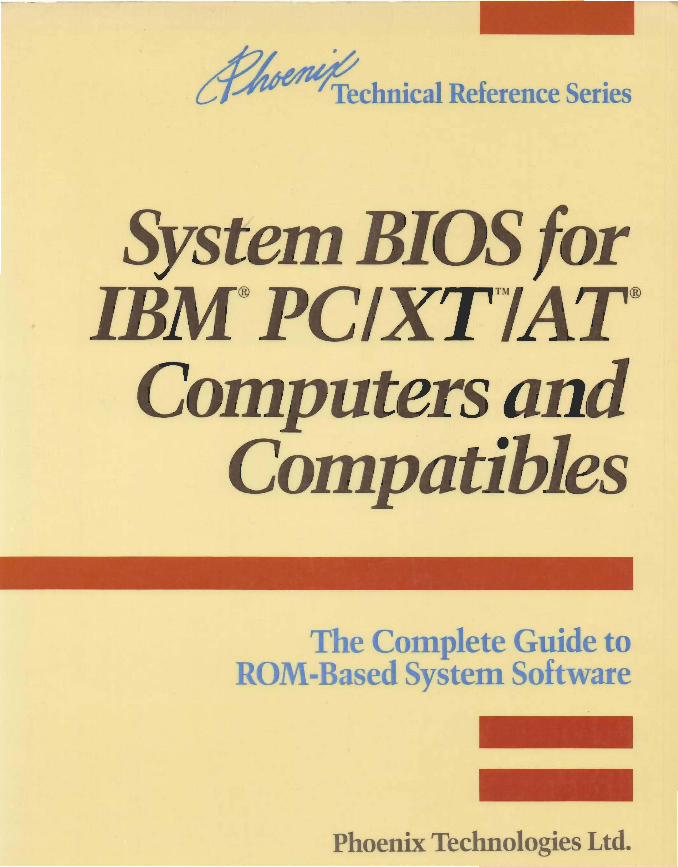

Technical Reference Series
System BIOS for IBM® PCI)(TrMIAT®
Computers and Compatibles
The Complete Guide to ROM-Based System Software
Phoenix Technologies Ltd.
A.... Addison-Wesley Publishing Company, Inc.
Reading, Massachusetts Menlo Park, California New York Don Mills, Ontario Wokingham, England Amsterdam Bonn
Sydney Singapore Tokyo Madrid San Juan
Many of the designations used by manufacturers and sellers to distinguish their products are claimed as trademarks. Where those designations appear in this book and Addison-Wesley was aware of a trademark claim, the designations have been printed in initial capital letters.
Limitation of Liability While every reasonable precaution has been taken in the preparation of this book, the author and the publishers assume nO responsibility for errors or omissions, or for the uses made of the material contained herein or the decisions based on such use. No warranties are made, express or implied, with regard to the contents of this work, Its merchantability, or fitness for a particular purpose. Neither the author nor the publishers shall be liable for direct, special, incidental, or consequential damages arising out of the use or inability to use the contents of this book.
Library of Congress Cataloglng-In-Publlcatlon Data
System BIOS for IBM PCIXTIAT computers and compatibles I Phoenix Technologies, Ltd.
p. cm. -- (Phoenix technical reference series) ISBN 0-201-51806-6 : 1.IBM Personal Computer. 2. IBM Personal Computer XT. 3. IBM
Personal Computer AT. 4. Operating systems (Computers) I. Phoenix Technologies. II. Title: BIOS. III. Series. QA76.8.12594S97 1989 004.4'469--dc20 89-17557
CIP
Copyright © 1989,1988,1987 by Phoenix Technologies Ltd.
All rights reserved. No part of this publication may be reproduced, stored in a retrieval system, or transmitted in any form or by any means, electronic, mechanical, photocopying, recording, or otherwise, without the prior written permission of the publisher. Printed in the United States of America. Published simultaneously in Canada.
Cover design by Hannus Design Associates Text design by Phoenix Technologies Ltd. Set in 10-point Modern by Phoenix Technologies Ltd.
ISBN: 0-201-51806-6 EFGHIJ-AL-93210
Fifth Printing, August 1990
Trademarks
This manual acknowledges the following trademarks:
Ashton-Tate and Framework are registered trademarks of Ashton-Tate Corporation.
AST Is a registered trademark of AST Research, Inc.
AT, IBM, Personal Systems/2, PS/2, and PC/AT are registered trademarks of the International Business Machines Corporation. PC-DOS, PC/XT, VGA, CGA, MCA, MDA, EGA, OS/2, and Micro Channel are trademarks of the International Business Machines Corporation.
Hercules, Hercules Graphic Card, and Hercules Graphic Adapter are trademarks of Hercules Computer Technology.
Intel Is a registered trademark of Intel Corporation.
1-2-3, Lotus, and Symphony are registered trademarks of Lotus Development Corp.
Motorola Is a registered trademark of Motorola Semiconductor Products, Inc.
MS, MS-DOS, XENIX, and Microsoft are registered trademarks of Microsoft Corporation.
NEC and Multisync are registered trademarks of Nippon Electric Corporation.
Quadram Is a registered trademark of Quadram Corporation.
Dedication
To the IBM engineers and programmers who designed and coded the IBM PC, XT, and AT BlOSs.
Table of Contents
Foreword ...................................................... xvii
About This Book ............................................... xxiii
Acronyms and Abbreviations . . . . . . . . . . . . . . . . . . . . . . . . . . . . . . . . . .. xxvii
Chapter 1 - The ROM BIOS
Overview .......................................................... 1 BIOS: Theory of Operation .................................. . . . . . . . . .. 4 BIOS Memory Usage ...............•................•.' . . . . . . . . . . . . . .. 8 Interrupt Vector Table. . . . . . . . . . . . . . . . . . . . . . . . . . . . . . . . . . . . . . . . . . . . . . .. 9 Unexpected Interrupt Handler •......................................... 12 System BIOS Functions and BIOS Diversity .............................. 14 Video BIOS Functions and BIOS Diversity ................................ 16 Summary: The BIOS Services ......................................... 18
Chapter 2 - System RAM Data
Overview .......................................................... 27 Interrupt Vectors .................................................... 28 BIOS Data Area ..................................................... 31 Power-On Self Test Definitions ........................................ 38 INT 1Oh Video Service Data Definitions .................................. 39 INT 11 h Equipment List Service Data Definitions .......................... 41 INT 12h Memory Size Service Data Definition ............................ 41 INT 13h Diskette Service Data Definitions ................................ 42 INT 14h Serial Communication Service Data Definitions .................... 45 INT 16h Keyboard Data Service Definitions and
INT 09h Keyboard Service Interrupt Data Definitions .................... 45 INT 17h Parallel Printer Service Data Definitions .......................... 47 INT 19h Bootstrap Loader Service Data Definitions ........................ 48 INT 1Ah Time-of-Day Service Data Definitions ........................... 48
continued
System BIOS for IBM PC/XTI AT Computers and Compatibles vii
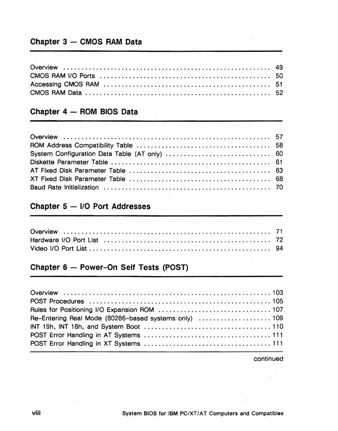
Chapter 3 - CMOS RAM Data
Overview ......................................................... 49 CMOS RAM I/O Ports ............................................... 50 Accessing CMOS RAM .............................................. 51 CMOS RAM Data . . . . . . . . . . . . . . . . . . . . . . . . . . . . . . . . . . . . . . . . . . . . . . . .. . .. 52
Chapter 4 - ROM BIOS Data
Overview ......................................................... 57 ROM Address Compatibility Table ..................................... 58 System Configuration Data Table (AT only) ............................. 60 Diskette Parameter Table . . . . . . . . . . . . . . . . . . . . . . . . . . . . . . . . . . . . . . . . . . .. 61 AT Fixed Disk Parameter Table ..................... ;................. 63 XT Fixed Disk Parameter Table ....................................... 68 Baud Rate Initialization .............................................. 70
Chapter 5 - 1/0 Port Addresses
Overview ......................................................... 71 Hardware I/O Port List .............................................. 72 Video I/O Port List . . . . . . . . . . . . . . . . . . . . . . . . . . . . . . . . . . . . . . . . . . . . . . . . .. 94
Chapter 6 - Power-On Self Tests (POST)
Overview ......................................................... 103 POST Procedures .................................................. 105 Rules for Positioning I/O Expansion ROM ............................... 107 Re-Entering Real Mode (80286-based systems only) .................... 109 INT 19h, INT 18h, and System Boot ................................... 110 POST Error Handling in AT Systems ................................... 111 POST Error Handling in XT Systems ................................... 111
continued
System BIOS for IBM PC/XT I AT Computers and Compatibles viii

Chapter 7 - INT 02h Nonmaskable Interrupt
Overview ......................................................... 113 XT NMI Handling ................................................... 115 8087 Coprocessor Exceptions ........................................ 116 AT NMI Handling ................................................... 117 80x87 Coprocessor Exceptions in AT Systems .......................... 119
Chapter 8 - INT 09h and INT 16h Keyboard Services
Overview ......................................................... 121 Theory of Operation ................................................ 123 Keyboard 1/0 Ports ................................................. 128 System RAM Data . . . . . . . . . . . . . . . . . . . . . . . . . . . . . . . . . . . . . . . . . . . . . . . . . . 129 INT 09h: Internal Function Requests ................................... 131 INT 09h: System Reset «Ctrl> <A It> <Del» ............................ 132 INT 09h: Break «Ctrl> <Break> or <Ctrl> <Scroll Lock» .................. 133 INT 09h: Pause «Ctrl> <Num Lock» .; ................................ 134 INT 09h: Print Screen «PrtSc> or <Shift> <PrtSc>) ...................... 136 INT 09h: System Request «SysReq» ................................. 137 INT 16h: Keyboard DSR ............................................. 138 INT 16h: AH = OOh Read Keyboard Input ............................... 139 INT 16h: AH = 01 h Return Keyboard Status ............................. 141 INT 16h: AH = 02h Return Shift Flag Status ............................. 142 INT 16h: AH = 03h Set Typematic Rate and Delay ....................... 143 INT 1 6h: AH = 05h Store Key Data .................................... 144 INT 16h: AH = 10h Read Extended Keyboard Input ....................... 145 INT 16h: AH = 11 h Return Extended Keyboard Status .................... 146 INT 16h: AH = 12h Return Extended Shift Flags Status .................... 147 How to Read Character Code Tables .................................. 149 Character Codes: AH = OOh/01 h ...................................... 151 Character Codes: AH = 1Oh/11 h ...................................... 156
Chapter 9 - INT 10h Video Service
Overview ......................................................... 161 Theory of Operation ............................•................... 164 MDA Hardware Environment .......................................... 174
continued
System BIOS for IBM PC/XTI AT Computers and Compatibles ix
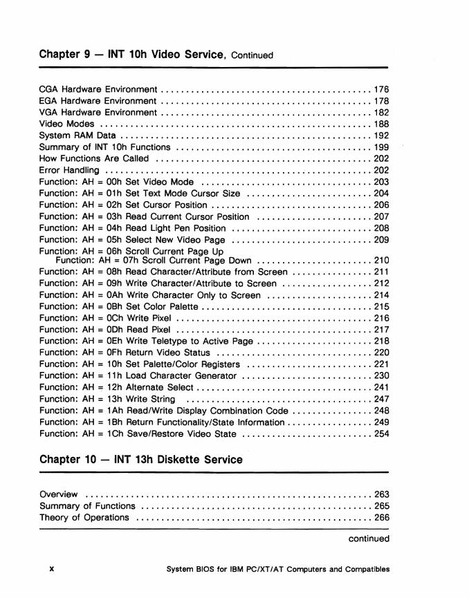
Chapter 9 - INT 10h Video Service, Continued
CGA Hardware Environment .......................................... 176 EGA Hardware Environment .................................•........ 178 VGA Hardware Environment .......................................... 182 Video Modes •.•......................•............................ 188 System RAM Data .....................................•............ 192 Summary of INT 10h Functions ............... , ....................... 199 How Functions Are Called .....................•..................... 202 Error Handling ........•.......................•.................... 202 Function: AH = OOh Set Video Mode .................................. 203 Function: AH = 01h Set Text Mode Cursor Size ......................... 204 Function: AH = 02h Set Cursor Position ..............•................. 206 Function: AH = 03h Read Current Cursor Position ....................... 207 Function: AH = 04h Read Light Pen Position .....•...................... 208 Function: AH = 05h Select New Video Page ............................ 209 Function: AH = 06h Scroll Current Page Up
Function: AH = 07h Scroll Current Page Down ............•.......... 210 Function: AH = 08h Read Character/Attribute from Screen ................ 211 Function: AH = 09h Write Character/Attribute to Screen .................. 212 Function: AH = OAh Write Character Only to Screen ..•.................. 214 Function: AH = OBh Set Color Palette .................................. 215 Function: AH = OCh Write Pixel ....................................... 216 Function: AH = ODh Read Pixel ....................................... 217 Function: AH = OEh Write Teletype to Active Page ....................... 218 Function: AH = OFh Return Video Status ......•........................ 220 Function: AH = 10h Set Palette/Color Registers .•....................... 221 Function: AH = 11 h Load Character Generator .•........................ 230 Function: AH = 12h Alternate Select ................................... 241 Function: AH = 13h Write String ..................................... 247 Function: AH = lAh Read/Write Display Combination Code ................ 248 Function: AH = 1Bh Return Functionality/State Information ................. 249 Function: AH = 1 Ch Save/Restore Video State .......................... 254
Chapter 10 - INT 13h Diskette Service
Overview ................•.................•...................... 263 Summary of Functions .............................................. 265 Theory of Operations .......................... , .................... 266
continued
System BIOS for IBM PC/XT I AT Computers and Compatibles x
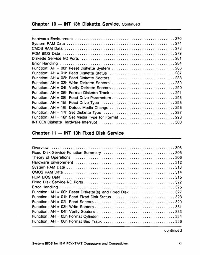
Chapter 10 - INT 13h Diskette Service, Continued
Hardware Environment .............................................. 270 System RAM Data .................................................. 274 CMOS RAM Data ................................................... 278 ROM BIOS Data .................................................... 279 Diskette Service I/O Ports ........................................... 281 Error Handling ..................................................... 284 Function: AH = OOh Reset Diskette System ............................. 286 Function: AH = 01 h Read Diskette Status .............................. 287 Function: AH = 02h Read Diskette Sectors ............................. 288 Function: AH = 03h Write Diskette Sectors ............................. 289 Function: AH = 04h Verify Diskette Sectors ............................. 290 Function: AH = 05h Format Diskette Track ...........................•. 291 Function: AH = 08h Read Drive Parameters ............................. 293 Function: AH = 15h Read Drive Type .................................. 295 Function: AH = 16h Detect Media Change .............................. 296 Function: AH = 17h Set Diskette Type ................................. 297 Function: AH = 18h Set Media Type for Format ......................... 298 INT OEh Diskette Hardware Interrupt ................................... 300
Chapter 11 - INT 13h Fixed Disk Service
Overview ......................................................... 303 Fixed Disk Service Function Summary ................................. 305 Theory of Operations ............................................... 306 Hardware Environment .............................................. 312 System RAM Data .................................................. 313 CMOS RAM Data ................................................... 314 ROM BIOS Data .................................................... 315 Fixed Disk Service liD Ports .......................................... 322 Error Handling ..................................................... 325 Function: AH = OOh Reset Diskette(s) and Fixed Disk .................... 327 Function: AH == 01 h Read Fixed Disk Status ............................. 328 Function: AH = 02h Read Sectors ..................................... 329 Function: AH = 03h Write Sectors ..................................... 331 Function: AH = 04h Verify Sectors .................................... 333 Function: AH = 05h Format Cylinder ................................... 334 Function: AH = 06h Format Bad Track ................................. 336
continued
System BIOS for IBM PC/XT/AT Computers and Compatibles xi

Chapter 11 - INT 13h Fixed Disk Service, Continued
Function: AH = 07h Format Drive ..................................... 337 Function: AH = 08h Read Drive Parameters ............................. 338 Function: AH = 09h Initialize Drive Parameters .......................... 340 Function: AH = OAh Read Long Sectors ................................ 341 Function: AH = OBh Write Long Sectors ................................ 343 Function: AH = OCh Seek to Cylinder .................................. 345 Function: AH = ODh Alternate Fixed Disk Reset .......................... 346 Function: AH = OEh Diagnostics 1: Read Test Buffer ..................... 347 Function: AH = OFh Diagnostics 2: Write Test Buffer ..................... 348 Function: AH = 10h Test for Drive Ready ............... " .............. 349 Function: AH = 11 h Recalibrate Drive .................................. 350 Function: AH = 12h Controller RAM Diagnostic .......................... 351 Function: AH = 13h Controller Drive Diagnostic .......................... 352 Function: AH = 14h Controller Internal Diagnostic ........................ 353 Function: AH = 15h Read Fixed Disk Type .............................. 354
Chapter 12 - INT 14h Serial Communications Service
Overview ......................................................... 357 Theory of Operation ................................................ 359 System RAM Data .................................................. 365 ROM BIOS Data .................................................... 366 Serial Communications 110 Ports ...................................... 367 Error Conditions .................................................... 373 Function: AH = OOh Initialize Serial Communications Port .................. 374 Function: AH = 01h Send Character ................................... 376 Function: AH = 02h Receive Character ................................. 377 Function: AH = 03h Read Serial Port Status ............................ 378
Chapter 13 - INT 15h System Services
Overview ......................................................... 379 Summary of Functions ..•........................................... 381 Hardware Environment .............................................. 382 System RAM Data .................................................. 382 CMOS RAM Data ................................................... 383
continued
xii System BIOS for IBM PC/XT I AT Computers and Compatibles
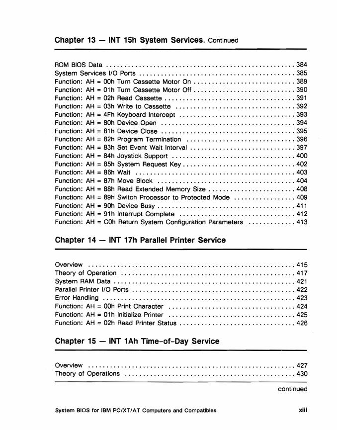
Chapter 13 - INT 15h System Services. Continued
ROM BIOS Data ..................••............•..•................ 384 System Services I/O Ports .........•...............•................. 385 Function: AH = OOh Turn Cassette Motor On ............................ 389 Function: AH = 01 h Turn Cassette Motor Off ............................ 390 Function: AH = 02h Read Cassette •..........................•........ 391 Function: AH = 03h Write to Cassette ...••............................ 392 Function: AH = 4Fh Keyboard Intercept ..........................•..... 393 Function: AH = 80h Device Open ...............•.•................•.. 394 Function: AH = 81 h Device Close ..................................... 395 Function: AH = 82h Program Termination ......•....................... 396 Function: AH = 83h Set Event Wait Interval ............................. 397 Function: AH = 84h Joystick Support ............•...••................ 400 Function: AH = 85h System Request Key ............................... 402 Function: AH = 86h Wait ...........••............................... 403 Function: AH = 87h Move Block ...................................... 404 Function: AH = 88h Read Extended Memory Size ........................ 408 Function: AH = 89h Switch Processor to Protected Mode ....•............ 409 Function: AH = 90h Device Busy ...................................... 411 Function: AH = 91 h Interrupt Complete ................................ 412 Function: AH = COh Return System Configuration Parameters ............. 413
Chapter 14 - INT 17h Parallel Printer Service
Overview ...............•......................................•.. 415 Theory of Operation ................................................ 41 7 System RAM Data .................................................. 421 Parallel Printer I/O Ports ..................................•.......... 422 Error Handling ..................................................... 423 Function: AH = OOh Print Character .•...........•..................... 424 Function: AH = 01 h Initialize Printer ...............•••................. 425 Function: AH = 02h Read Printer Status ..........•.••.................. 426
Chapter 15 - INT 1Ah Time-of-Day Service
Overview ..........••.............•............................... 427 Theory of Operations .............................•................. 430
continued
System BIOS for IBM PC/XT/AT Computers and Compatibles xiii
Chapter 15 - INT 1Ah Time-of-Day Service, Continued
System RAM Data .................................................. 434 CMOS RAM Data ................................................... 434 Time-at-Day Service 1/0 Ports ....................................... 436 Error Handling ..................................................... 437 Function: AH = ~Oh Read System Timer Time Counter ................... 438 Function: AH = 01 h Set System Timer Time Counter ..................... 439 Function: AH = 02h Read Real Time Clock Time ........................ 440 Function: AH = 03h Set Real Time Clock Time .......................... 441 Function: AH = 04h Read Real Time Clock Date ........................ 442 Function: AH = 05h Set Real Time Clock Date .......................... 443 Function: AH = 06h Set Real Time Clock Alarm ........................ 444 Function: AH = 07h Reset Real Time Clock Alarm ....................... 445 Function: AH = 80h Set Sound Source ................................. 445 INT 08h System Timer ISR ........................................... 446 INT 70h Real Time Clock ISR ......................................... 449 INT 1Ch Timer Tick ISR .............................................. 452 INT 4Ah Alarm ISR .................................................. 452
Chapter 16 - Single Function BIOS Services
Overview ......................................................... 453 INT 05h Print Screen Service ......................................... 455 INT 11 h Equipment List Service ....................................... 457 INT 12h Memory Size Service ........................................ 458 INT 19h Bootstrap Loader Service ..................................... 459
Appendix A - AT BIOS Error Codes and Messages
Introduction ........................................................ 463 IBM BIOS POST and Boot Messages ................................... 464 Phoenix BIOS POST and Boot Messages ............................... 466 Phoenix BIOS Run-Time Messages .................................... 470 Phoen~ BIOS Beep Codes ........................................... 471 SETUP Messages ................................................... 477
continued
System BIOS for IBM PC/XT/AT Computers and Compatibles xiv
Appendix B - XT BIOS Error Messages
Introduction .••..•..............................•.................. 479 Beep Code ........................................................ 480 IBM XT BIOS POST Messages ...........•...............•..•......... 480 Phoenix XT BIOS POST and Boot Messages ...............•............. 481 Phoenix XT BIOS Run-Time Messages ................................. 484
Glossary ............................................ , ........... 485
Additional Resources ........................................... 493
Index .. .......................................................... 495
System BIOS for IBM PC/XT/AT Computers and Compatibles xv


Foreword
The Micro Revolution
The personal computer has come a long way from being a hacker's hobby in basements and garages to a multibillion-dollar industry. In the early days, programming carried with it an aura of history-in-the-making, of a revolution that would alter not only the business world, but the fabric of society as well. In the personal computer, we had found a new vehicle for the exchange of ideas and the formation of a global village. Personal computing promised to democratize technology.
At that time, the structure of computing environments centered around the mainframe. Mainframes cost millions of dollars, filled up large air-conditioned rooms and required a host of programmers to appease and maintain them. Users who wished to supplicate the mainframe for a specific task were forced to request an audience through their Management Information Systems group. They then had to wait months and even years for their applications to be built and run, often sacrificing precious time and frustrating their creative spirits.
I was an undergraduate at M.I.T. when I first heard of the microprocessor. It was the key to the computer kingdom that all hackers dreamt about, a way to bring computing power to individuals without the intervention of bureaucracies. The microprocessor created a cult following among programmers.
System BIOS for IBM PC/XT/AT Computers and Compatibles xvii
In the mid-seventies, large computer companies, built around the proprietary technology of their mainframes and minicomputers, down played the micro's potential. As often happens in the business world, it took a group of visionaries and entrepreneurs to capitalize on that potential and to create an industry around it.
Once the market had been formed, though, the computer establishment realized there was gold in those silicon hills and valleys and rushed to enter. It was actually just what the fledgling industry needed: someone with the marketing clout to establish a standard platform. One cannot advance technology without a platform to serve as a basis for expansion and evolution into higher forms.
Thus, the IBM PC was born, and with it the era of DOS.
BIOS: The Missing Link
I founded Phoenix in 1979 as a supplier of programmers' tools to support the DOS standard. We were successful, but not a phenomenon until we broke through with the PC ROM BIOS in May 1984. It proved to be the missing link for manufacturers to build systems that were 100 percent compatible with the IBM PC and, just as important, 100 percent legal.
Our "clean room" methodology was responsible. "Contaminated" engineers studied the BIOS' functionality and passed on those functions to "virgin" engineers, who had never seen the BIOS and who then wrote the code that would accomplish specific tasks. I am proud to say the Phoenix ROM BIOS was one of the keys that unlocked the PC market and enabled it to grow to its present proportions.
Phoenix was your archetypal start-up. The first bus architecture that Phoenix supported was the VW platform as it was driven from one programmer's garage to another's basement, picking up products and orders for our initial line of programmers' tools. Our corporate meeting room was in a basement. I would lead visiting computer executives down a narrow stairwell to a dark basement, where they would share an old sofa with a bunch of cats, shedding hairs all over their pinstriped suits. That was three office buildings ago, and we're still growing.
Over 300 companies have licensed our ROM BIOS. Today, there are more installed Phoenix BlOSs than IBM's, with over 14 million systems booting up with the Phoenix name as the first item to appear on screen.
System BIOS for IBM PC/XT/AT Computers and Compatibles xviii

Our engineering ventures did not end with the BIOS. Since the PC standard is always changing, compatibility is a moving target. In fact, the BIOS has been an evolving piece of indispensable code which has been continually upgraded to maintain a system's compatibility with the advancements of the PC's capabilities.
Phoenix also helped to pioneer emulation technologies that enable technical and graphical workstations to become DOS compatible. Our software coprocessor technology is one of the key reasons UNIX workstations are currently enjoying their acceptance in mainstream computing environments. Our latest product development, PhoenixPage, is a systems software suite that supports printer standards, such as PostScript-language compatibility.
Portrait of a Company as a Young BIOS
Phoenix is in the middle of the micro madness, but with a method. Phoenix's strategy is based on the revolution at the heart of the computer industry's dynamic growth. The emergence of open standards has drastically altered the way we do business with advanced technologies. Contrary to the conventional wisdom that looked for a market edge through the development of proprietary technologies, companies are realizing that industry-wide adoption of standards is a prerequisite for growth, both in technical and financial terms.
The diversification of the Phoenix product line revolves around a central concept: the promulgation of open standards. In the current proliferation of operating systems, CPUs, chip sets, system board configurations, and bus architectures, Phoenix's flexible systems software gives a manufacturer freedom of design and end users the assurance of quality compatibility.
The BIOS itself may serve as a perfect business model in understanding Phoenix's role in the microcomputer revolution. Just like systems-level components in the architecture of a computer, there are players in the computer industry that are mainly invisible to end users, but who possess roles that are crucial to the smooth execution of product cycles and advancing technologies.
Just as the BIOS sits at the heart of the PC, where software meets hardware, and interfaces communications between the operating system, CPU, and a computer's peripheral devices (monitor, printer, disk drives, etc.), so Phoenix is positioned at the center of the PC universe, working closely with semiconductor, hardware, and peripheral manufacturers; operating system and independent software developers; and system integrators, ensuring compatible designs among them all, peace of mind for purchasers and end users, and a stable and open platform for programmers.
System BIOS for IBM PC/XT I AT Computers and Compatibles xix

PC Compatibility: The Only Game in Town
The PC standard is now entirely software-driven. It is not dependent on IBM's hardware architecture. The goal of a standard is not IBM hardware emulation, but a hardware-independent compatibility based on the ability to run PC applications. It was as much to achieve compatibility with each other as with IBM that caused most of the industry's largest manufacturers (some of whom once shunned PC compatibility) to jump on the bandwagon.
The value of compatibility with the PC standard from the end user's viewpoint is that it offers investment protection, portability, and access to the world's largest library of applications software packages. These considerations have made 100 percent compatibility the main customer-driven demand in the personal computer marketplace.
In the past few years, the PC industry has seen phenomenal growth. Now that the standard has been established, the platform is in place to launch an even more impressive and expansive future. The goal for software developers is to break away from hardware-imposed stagnation and push the PC environment to new heights. Phoenix's biggest challenge as a company will be to help manufacturers and software developers integrate compatibility into new products with smart, innovative engineering.
Open Sesame
Standards advance technology. The establishment of a common platform enables hardware and software developers to evolve more advanced technologies, since they now have a target and a customer base to make it worthwhile. The adoption of standards frees engineering resources to concentrate on differentiating products with expanded capabilities.
Phoenix's goal has always been to support standards in the micro environment. Open standards enable an industry to reap the rewards of advanced technology by attracting the widest possible customer base and applications. Phoenix provides a cost-effective engineering resource to solve the integration challenges the PC industry faces.
We are offer.ing this series of BIOS technical references in the same spirit of .. openness" that has characterized our research and development, from the days of our programmers' tools through the introduction of our PC BIOS and creation of the compatibles market.
Open systems need open communications. For personal computing to succeed in society, information must be readily available to allow individuals to exploit its capabilities. These manuals provide a complete and clear picture of the design of the PC standard. They describe the parameters of compatibility and how best to design a system based on the standard.
System BIOS for IBM PC/XT I A T Computers and Compatibles xx
Programmers will find a treasure trove between these covers. They will have easy access to the PC architecture and will have a secure and stable platform to which to write. My hope is that these manuals will help put the personal back into computing.
Neil J. Colvin
Chairman Phoenix Technologies Ltd.
System BIOS for IBM PC/XT/AT Computers and Compatibles xxi


About This Book
What this book is about
System BIOS for IBM PCIXTIAT Computers and Compatibles is a detailed technical reference that describes the BIOS. the component of PC. XT. and AT systems that insulates both applications software and single-tasking operating systems. such as MS-DOS. from direct manipulation of PC hardware. The information provided in this book is applicable to all PC. XT. and AT computers and compatibles.
Who should read this book
System BIOS for IBM PCIXTIAT Computers and Compatibles provides the most comprehensive source of information about IBM PC. XT. and AT and compatible BlOSs available today. It can be used by anyone interested in learning more about IBM or compatible computers.
Applications programmers and device driver developers will find a thorough discussion of each BIOS device service and function. including all levels of video BIOS. from MDA and CGA through EGA and VGA. In addition. System BIOS for IBM PCIXTIAT Computers and Compatibles defines. to the bit level. all IBM and compatible 110 port addresses and BIOS-related CMOS RAM and system RAM data.
Hardware technicians and other system troubleshooters will appreciate the complete list of all BIOS-generated error messages. their likely causes. and suggested solutions.
System BIOS for IBM PC/XTI AT Computers and Compatibles xxiii

Other volumes in this series
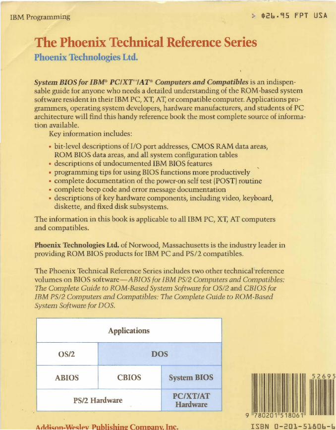
System BIOS for IBM PC/XTIAT Computers and Compatibles is one of several volumes about BIOS software in the Phoenix Technical Reference Series. Other volumes are:
ABIOS for IBM PS/2 Computers and Compatibles - a complete technical reference describing the portion of a PS/2 BIOS that supports multitasking operating systems such as OS/2.
CBIOS for IBM PS/2 Computers and Compatibles - a complete technical reference describing the portion of a PS/2 BIOS that supports single-tasking operating systems such as DOS.
The volumes of this series are a natural companion for anyone who owns and programs an IBM PC, XT, AT, or PS/2, or any compatible system.
How to find information
System BIOS for IBM PC/XT/AT Computers and Compatibles is organized into several major parts. Chapter 1 provides a general summary of BIOS concepts. Chapters 2-6 describe BIOS and system data definitions and I/O port usage. Chapters 7-16 describe the individual BIOS services and serve as a technical reference. Appendixes A and B provide comprehensive lists of potential error messages for AT and XT -compatible systems.
Each service-specific chapter (7-16) is organized in the same way. There is a description of the service and the theory of operations for this service, a list of all I/O ports and data definitions accessed by the service, a discussion on how errors are handled for this service, and complete descriptions of each service function. The function descriptions include an explanation of what the function does, the function's required inputs and outputs, and any special programming considerations.
A word about diversity
In the eight years since the original PC emerged, there have been countless manufacturers of PC, XT, and AT systems and BIOS products. Although all BlOSs in IBM-compatible microcomputers by definition have to be compatible with the IBM standard, there has been a good deal of diversity in the detail of BIOS architecture.
This diversity makes it difficult to precisely identify terms such as PC-, XT-, or AT-compatible. BIOS functions that appear only in IBM AT systems can be found in the Phoenix XT BIOS. And there are many different combinations of BIOS functions in various XT or AT clones. Whenever possible, we provide directions on how to find out if a particular function is supported.
System BIOS for IBM PC/XT/AT Computers and Compatibles xxiv

What we assume you know
This book assumes a basic knowledge of 8086. 80286. and 80386 assembly language programming concepts. PC architecture. and operating system concepts. If you are new to these subjects. you may want to refer to the introductory texts listed at the end of this book.
Acknowledgments
First and foremost. we would like to acknowledge the vision and technical skill of Neil Colvin. founder. Chairman of the Board and Chief Technical Officer of Phoenix Technologies Ltd. We also acknowledge the expert guidance of Lance Hansche. President and CEO of Phoenix Technologies Ltd.
We especially want to acknowledge the contributions made by Jeff Bobzin. Dave Hirschman. and Bob Vandette - the Phoenix engineers who initially brought the BIOS to life. as well as the continuing efforts of Eric Enge. Paula Bishop. Jeff Kleiman. Debbie Schultz. Stan Lyness. Greg Honsa. Bruce Cairns. Ruth Brent. Jeff Wheeler. and the rest of the Phoenix staff. who keep the BIOS alive and compatible with the widest range of PC hardware.
This volume could not have been produced without the tireless efforts of Rich Levandov. Vice President of Marketing. and Henry Suwinsky. Project Manager.
We would like to thank Kathy Schiff. Manager of Technical Communications. who provided editorial guidance and direction in the production of this book and Jeff Evangelista. who contributed two well-written chapters. And last but not least. our special thanks goes to Sandie Zierak. Chief Production Coordinator. for her invaluable contributions in document design. graphics, and production.
The Authors
Mike Boston Paul Narushoff
Phoenix Technologies Ltd. Norwood, MA May. 1989
System BIOS for IBM PC/XTIAT Computers and Compatibles xxv

I I I I I I I I I I I I I I I I I I I I I I I I I I I I I I I I I I I I I I I I I I I I I I I I I I I I I I I I I
II III III IIIII I III III II
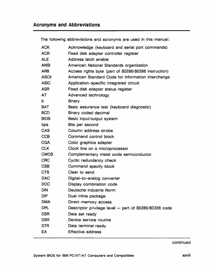
Acronyms and Abbreviations
The following abbreviations and acronyms are used in this manual:
ACK
ACR
ALE
ANSI
ARB
ASCII
ASIC
ASR
AT
b
BAT
BCD
BIOS
bps
CAS
CCB
CGA
ClK CMOS
CRC
CSB
CTS
DAC
DCC
DIN
DIP
DMA
DPl
DSR
DSR
DTR
EA
Acknowledge (keyboard and serial port commands)
Fixed disk adapter controller register
Address latch enable
American National Standards organization
Access rights byte (part of 80286/80386 instruction)
American Standard Code for Information Interchange
Application-specific integrated circuit
Fixed disk adapter status register
Advanced technology
Binary
Basic assurance test (keyboard diagnostic)
Binary coded decimal
Basic input/output system
Bits per second
Column address strobe
Command control block
Color graphics adapter
Clock line on a microprocessor
Complementary metal oxide semiconductor
Cyclic redundancy check
Command specify block
Clear to send
Digital-to-analog converter
Display combination code
Deutsche Industrie Norm
Dual inline package
Direct memory access
Descriptor privilege level
Data set ready
Device service routine
Data terminal ready
Effective address
part of 80286/80386 code
continued
System BIOS for IBM PC/XT/AT Computers and Compatibles xxvii

Acronyms and Abbreviations, Continued
EBCDIC
ECC
EGA
EIA
EISA
EOI
EPL
EPROM
ESDI
ETB
FCB
GDT
h
ICW
INT
I/O
IRQ
IRET
ISA
ISR
ISR
K Kbs
LDT
LDTR
LED
LID
LSB
LSI
M, MB
MDA
MFM
MHz
xxviii
Extended Binary Coded Decimal Interchange
Error checking and correction
Enhanced graphics adapter
Electronic Industries Association
Extended industry standard architecture
End of interrupt
Extended privilege level
Erasable programmable read-only memory
Enhanced small device interface
End of transmission block
Format control block - disk I/O data structure
Global descriptor table
Hexadecimal
Interrupt control word
Interrupt
Input/Output
Interrupt request line or Interrupt request
Return from an interrupt
Industry standard architecture
Interrupt service routine
Interrupt status register
Kilobytes
Kilobits per second
Local descriptor table
Local descriptor table register
Light-emitting diode
LogicallD
Least significant byte (or bit)
Large scale integration
Megabytes
Monochrome display adapter
Modified frequency modulation
Megahertz
continued
System BIOS for IBM PC/XT/AT Computers and Compatibles

Acronyms and Abbreviations, Continued
MMU
MSB
NCB
NMI OCW
OS/2
PC
PCLK
PEL PGA
PIC
PIO
PIT
POR
POST
PTL
RAM
RAS
RGB RI
RLL
ROM
RS-232C
RTC
RTS
SCSI
SOLC
SIMM
SIP
SMD
SSB
TSS
TIL
Memory management unit Most significant byte (or bit)
Network control block
Nonmaskable interrupt Operation control word
Operating System/2
Personal computer
Peripheral clock
Picture element (pixel) Professional graphics adapter
Programmable interrupt controller
Programmed input/output
Programmable interrupt timer
Power-on reset
Power-on self test
Phoenix Technologies Ltd.
Random access memory
Row address strobe
Red-Green-Blue (type of color generator) Ring indicator
Run length limited Read-only memory
Recommended standard-232C (serial controller interface)
Real time clock
Request to send
Small computer systems interface
Synchronous data link communications Single inline memory module
Single inline package
Surface-mount device Sense summary block - a disk I/O structure
Task state segment
Transistor-to-transistor logic
continued
System BIOS for IBM PC/XT/AT Computers and Compatibles xxix
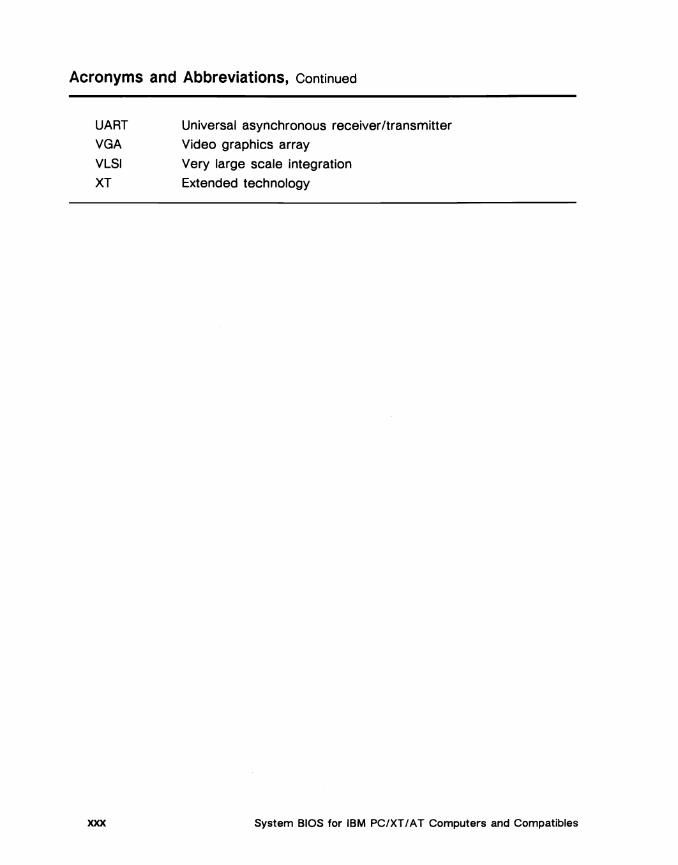
Acronyms and Abbreviations, Continued
UART Universal asynchronous receiver/transmitter VGA Video graphics array
VLSI Very large scale integration XT Extended technology
xxx System BIOS for IBM PC/XT / AT Computers and Compatibles
Chapter 1
The ROM BIOS
Overview
What is a BIOS?
A basic input output system (BIOS) is the lowest level software component of a computer's operating system. In personal computer systems, the BIOS usually consists of a routine designed to test system hardware and bootstrap load the operating system and a group of device drivers that service system liD components, such as the keyboard, the display, fixed disk drive, diskette drives, real time clock, parallel ports, serial ports, and other components.
Two methods for implementing BIOS
There are two methods for implementing a BIOS. The BIOS can be incorporated directly into system software and delivered on diskette as an integral part of the operating system. Or, the BIOS can be tied directly to the system hardware, programmed into ROM on the motherboard or on an expansion card.
continued
The ROM BIOS
Overview, Continued
Advantage of the ROM BIOS
As long as the interface between the operating system and the BIOS is standardized, programming the BIOS into ROM has the advantage of allowing system hardware to evolve independently from the operating system. When the BIOS is tied directly to the operating system, however, the operating system must be modified each time there is a change in system hardware.
PC ROM BIOS
The original IBM PC, a system based on the the 8/16-bit Intel 8088 microprocessor, was introduced in 1981. The IBM PC/XT, a fixed disk capable version of the PC, was introduced in 1983. The IBM PC/AT, a 16-bit system based on the Intel 80286 microprocessor, was introduced in 1984. Clone manufacturers have added Intel 80386-based AT-compatible systems. The BlOSs for all these systems are compatible, in the sense that the later AT BlOSs support all PC and XT BIOS functions in some way.
The BIOS in all models and versions of the IBM PC/XT / AT family of personal computers is programmed into ROM contained on the motherboard. The video BlOSs supporting the EGA and VGA PC video adapters are an exception to this rule. The EGA and VGA BlOSs are programmed into ROM contained on EGA and VGA adapter cards.
DOS: the PC operating system
PC-DOS, or MS-DOS - its Microsoft Corporation counterpart, is a singletasking operating system capable of addressing the 1 megabyte real mode address range of IBM PC/XT / AT systems. Introduced along with the original IBM PC in 1981, PC-DOS/MS-DOS has emerged as the predominant PC operating system. Both PC- and MS-DOS interface with the ROM BIOS instead of directly with system hardware. Programs that interface with DOS services or directly with the BIOS are assured the highest degree of hardware independence.
continued
System BIOS for IBM PC/XT/ AT Computers and Compatibles 2
Overview, Continued E
OS/2 and the ROM BIOS
In 1987. IBM introduced OS/2. a multitasking operating system designed for 16-bit PCs. When implemented on IBM PS/2 systems. OS/2 interfaces with the ABIOS portion of the PS/2 ROM BIOS. Although OS/2 can operate on AT class machines. it does not interface with the AT ROM BIOS. There is no BIOS support for OS/2 on an AT. so the level of support usually provided by the BIOS must be built into OS/2. Since OS/2 on an AT must interface directly with the computer hardware. there is a minimal level of portability from system to system with the AT version of OS/2.
Reference: For more information on the ABIOS. see ABIOS for IBM PS/2 Computers and Compatibles in this series.
Terminology used in this book
With the introduction of IBM PC/XT/AT compatible hardware and of IBM PC/XT/AT compatible ROM BlOSs (such as the Phoenix Technologies Ltd. 80x86 ROM BlOSs) came an entire PC "clone" industry. Like their IBM counterparts. the clones also contained a system board ROM BIOS.
Because of their sheer number. keeping track of PC clone model names can be confusing. In this book, "PC" refers to the IBM Personal Computer and compatible systems; "PC/XT" refers to the IBM Personal Computer/XT and compatibles. and "PC/AT" refers to the IBM Personal Computer/AT and compatibles. The terms PC BIOS. XT BIOS. and AT BIOS correspond to the ROM BIOS contained in each of those systems and their compatibles.
What this chapter is about
This chapter presents a general introduction to the concepts and design features of the IBM PC/XT/ATand compatible ROM BIOS.
The following topics are discussed:
• BIOS: Theory of Operation
• BIOS Memory Usage
• Interrupt Vector Table
• Unexpected Interrupt Handler
• System BIOS Functions and BIOS Diversity
• Summary: The BIOS Services
The ROM BIOS 3
BIOS: Theory of Operation
Background
All IBM PC/XT/AT and compatible computer systems are based on the Intel 80x86 or compatible microprocessors. To understand the BIOS architecture, one must consider the interrupt-driven nature of the Intel 80x86 architecture.
In Intel 80x86-based systems, interrupts can be generated by the microprocessor, by system hardware, or by software.
When an interrupt occurs, control of the computer is transferred to an interrupt handling routine. Once the routine has executed, the processor's program counter and flag register are returned to their previous state.
Where the ROM BIOS fits in
The majority of the ROM BIOS lID drivers proviae low level device services to the operating system and application programs running on the system. This kind of BIOS lID driver is invoked exclusively by software interrupt.
The remaining few ROM BIOS lID services provide direct support for system hardware; they are called via a hardware Interrupt.
BIOS services that are driven by software interrupt are referred to as ROM BIOS device service routines (DSR) , or more commonly by the name of the device involved. The ROM BIOS Video DSR, for example, is commonly referred to as the ROM BIOS Video Service. BIOS hardware driven services are referred to as hardware interrupt service routines (ISR).
Understanding the ROM BIOS is largely a matter of understanding how the BIOS device services fit into the Intel 80x86 scheme of interrupts.
continued
System BIOS for IBM PC/XT I AT Computers and Compatibles 4

BIOS: Theory of Operation, Continued
Facts about interrupts
Be it microprocessor, hardware, or software, every 80x86 interrupt is assigned a unique interrupt number ranging from OOh to FFh. By convention and to maintain IBM compatibility, certain ranges of interrupt numbers are reserved for special use. The software interrupt numbers ranging from 20h - 3Fh, for example, are reserved for the operating system (usually PC- or MS-DOS). End user software interrupts fall in the ranges 60h - 67h and F1h-FFh.
Each interrupt number is associated with one interrupt vector. An interrupt vector is the double word, segment:offset address of the routine assigned to an interrupt number. Interrupt vectors are stored in a table in memory beginning at address OO:OOh. The vector for INT OOh is stored at location OO:OOh to OO:03h; the address for INT 02h is stored at address OO:04h, and so forth.
In a process called the power-on self test (POST), the portion of the ROM BIOS responsible for testing system components and booting the operating system writes the interrupt vector table to low memory and initializes the vector address of all those interrupts concerned with the BIOS. When the operating system is booted, it, in turn, initializes all those interrupt vectors concerned with DOS. Users calling the BIOS from applications programs must take care to initialize the vectors concerned with their own interrupts.
continued
The ROM BIOS 5

BIOS: Theory of Operation, Continued
Interrupt ranges, types, and uses
The table below defines the range of interrupt numbers reserved for each interrupt type. It also summarizes how the various types of interrupts are invoked.
Type Description
Processor Microprocessor, or logical. Interrupts are Invoked by the processor as a result of some unusual program result. such as a program attempt to divide by zero.
• INTs OOh-04h are reserved for the processor.
Hardware Hardware interrupts are Invoked by peripheral devices by setting their respective Interrupt Request Line (IRQ). Each time a key is pressed. for example. the keyboard hardware generates a hardware Interrupt. Hardware Interrupts are vectored to Interrupt service routines (ISR) that generally reside In the BIOS.
· INTs OBh-OFh and 70h-77h are reserved by the BIOS.
Software Software interrupts are invoked via the assembly language "INT" mnemonic. Most software interrupts are vectored to device service routines (OSR) located In the ROM BIOS or in ~OS. There are three exceptions to this rule. however.
BIOS software INTs 1Dh, 1Eh, and 46h do not service a par· ticular device, but act instead to return various ROM-resident hardware parameter tables.
· INTs 20h-3Fh are reserved for ~OS.
• INTs OSh, 10h-1Ah. 1Dh-1Fh. 40h, 41h, 43h, and 46h are reserved for the BIOS.
User User Interrupts are a special class of software interrupt. They are invoked In the same way as software interrupts are. That is. through the INT mnemonic.
· INTs 60h-67h and INTs F1 h-FFh are reserved for user interrupt routines.
Reference: The contents of the interrupt vector table, as initialized by the ROM BIOS, are listed under the heading Interrupt Vector Table in this chapter. A discussion of how the ROM BIOS handles unexpected interrupts is found under the heading Unexpected Interrupt Handler.
continued
System BIOS for IBM PC/XT I AT Computers and Compatibles 6

BIOS: Theory of Operation, Continued
Calling ROM BIOS services/functions
Each ROM BIOS DSR is associated with one entry in the interrupt vector table. The ROM BIOS Video Service is vectored to INT 10h, the ROM BIOS Parallel Printer Service is vectpred to INT 17h, and so on.
Most of the BIOS DSRs are capable of executing more than one device related routine, or function. Individual functions within a device service are identified by a hex number and are selected by specifying that number in the AH register when the service is invoked. (Some ROM BIOS DSRs also contain subfunctions. Subfunctions are usually selected via the AL or BL registers.)
In addition to function numbers, all other parameters are passed to and from BIOS functions via the microprocessor registers. All BIOS device services save the program counter registers, the flag register, and all other registers except the AX register and those registers that return a value to the caller.
Reference: A complete list of the ROM BIOS DSRs, their associated interrupts, and functions is found under the heading Summary: The BIOS Services in this chapter.
Example program
The assembly language program below uses INT 10h Video Service function AH = 02h Set Cursor Position to move the cursor on video page 0 to row 3, column 14.
MOV AH, 2 ;Select "Set Cursor Position" function MOV DH, 3 ;Input row parameter into DH register MOV DL, 14 ;Input column parameter into DL register INT 10H ;Invoke INT 10h, BIOS Video Service
The ROM BIOS 7
BIOS Memory Usage
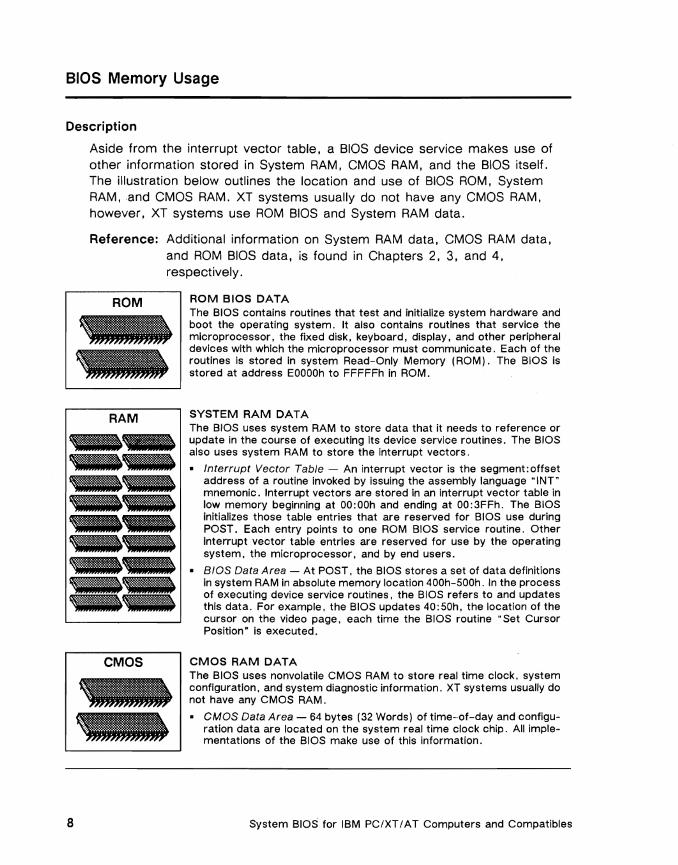
Description
Aside from the interrupt vector table, a BIOS device service makes use of other information stored in System RAM, CMOS RAM, and the BIOS itself. The illustration below outlines the location and use of BIOS ROM, System RAM ,and CMOS RAM. XT systems usually do not have any CMOS RAM, however, XT systems use ROM BIOS and System RAM data.
Reference: Additional information on System RAM data, CMOS RAM data, and ROM BIOS data, is found in Chapters 2, 3, and 4, respectively.
ROM ROM BIOS DATA The BIOS contains routines that test and initialize system hardware and boot the operating system. It also contains routines that service the microprocessor, the fixed disk, keyboard, display, and other peripheral devices with which the microprocessor must communicate. Each of the routines is stored in system Read-Only Memory (ROM). The BIOS Is stored at address EOOOOh to FFFFFh in ROM.
SYSTEM RAM DATA The BIOS uses system RAM to store data that it needs to reference or update in the course of executing its device service routines. The BIOS also uses system RAM to store the interrupt vectors.
Interrupt Vector Table - An interrupt vector is the segment:offset address of a routine invoked by issuing the assembly language "INT" mnemonic. Interrupt vectors are stored in an interrupt vector table in low memory beginning at OO:OOh and ending at OO:3FFh. The BIOS initializes those table entries that are reserved for BIOS use during POST. Each entry points to one ROM BIOS service routine. Other interrupt vector table entries are reserved for use by the operating system, the microprocessor, and by end users.
BIOS Data Area - At POST, the BIOS stores a set of data definitions in system RAM in absolute memory location 400h-500h. In the process of executing device service routines, the BIOS refers to and updates this data. For example, the BIOS updates 40:50h, the location of the cursor on the video page, each time the BIOS routine "Set Cursor Position" is executed.
CMOS RAM DATA The BIOS uses nonvolatile CMOS RAM to store real time clock, system configuration, and system diagnostic information. XT systems usually do not have any CMOS RAM.
• CMOS Data Area - 64 bytes (32 Words) of time-of-day and configuration data are located on the system real time clock chip. A" implementations of the BIOS make use of this information.
System BIOS for IBM PC/XT/ AT Computers and Compatibles 8
Interrupt Vector Table
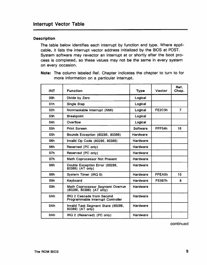
Description
The table below identifies each interrupt by function and type. Where applicable, it lists the interrupt vector address initialized by the BIOS at POST. System software may revector an interrupt at or shortly after the boot process is completed, so these values may not be the same in every system on every occasion.
Note: The column labeled Ref. Chapter indicates the chapter to turn to for more information on a particular interrupt.
Ref. INT Function Type Vector Chap.
OOh Divide by Zero Logical
01h Single Step Logical
02h Nonmaskable Interrupt (NMI) Logical FE2C3h 7
03h Breakpoint Logical
04h Overflow Logical
OSh Print Screen Software FFFS4h 16
OSh Bounds Exception (80286, 80386) Hardware
06h Invalid Op Code (80286, 80386) Hardware
06h Reserved (PC only) Hardware
07h Reserved (PC only) Hardware
07h Math Coprocessor Not Present Hardware
08h Double Exception Error (80286, Hardware 80386) (AT only)
08h System Timer (IRQ 0) Hardware FFEASh 15
09h Keyboard Hardware FE987h 8
09h Math Coprocessor Segment Overrun Hardware (80286, 80386) (AT only)
OAh IRQ 2 Cascade from Second Hardware Programmable Interrupt Controller
OAh Invalid Task Segment State (80286, Hardware 80386) (AT only)
OAh IRQ 2 (Reserved) (PC only) Hardware
continued
The ROM BIOS 9
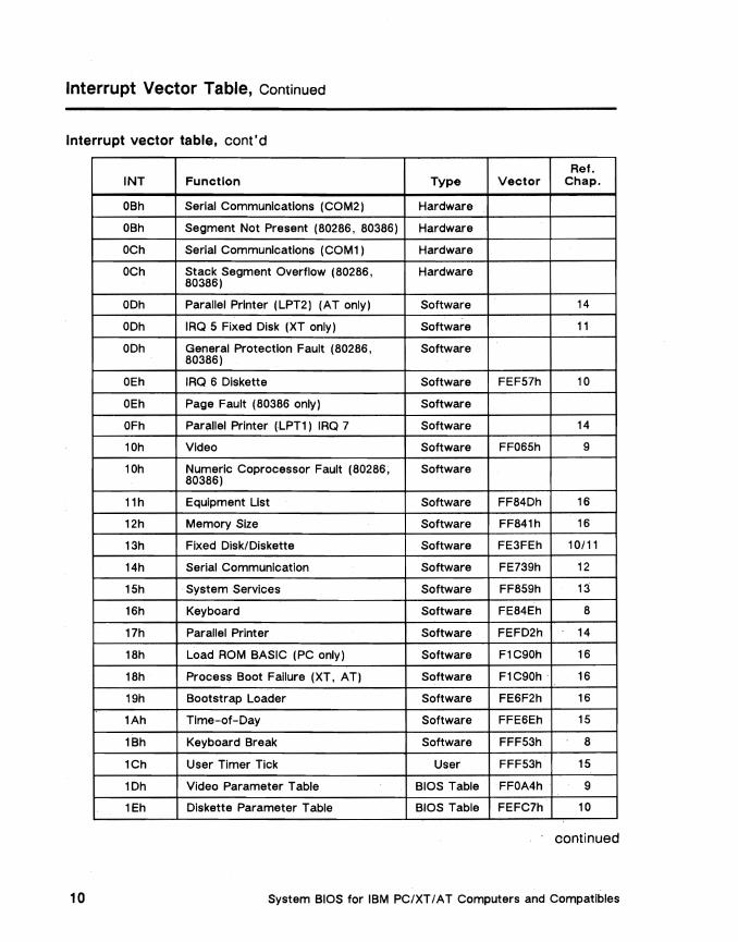
Interrupt Vector Table, Continued
Interrupt vector table, cont'd
Ref. INT Function Type Vector Chap.
OBh Serial Communications (COM2) Hardware
OBh Segment Not Present (80286, 80386) Hardware
OCh Serial Communications (COM1) Hardware
OCh Stack Segment Overflow (80286, 80386)
Hardware
ODh Parallel Printer (LPT2) (AT only) Software 14
ODh IRQ 5 Fixed Disk (XT only) Software 11
ODh General Protection Fault (80286, 80386)
Software
OEh IRQ 6 Diskette Software FEF57h 10
OEh Page Fault (80386 only) Software
OFh Parallel Printer (LPT1) IRQ 7 Software 14
10h Video Software FF065h 9
10h Numeric Coprocessor Fault (80286, 80386)
Software
11 h Equipment List Software FF84Dh 16
12h Memory Size Software FF841h 16
13h Fixed Disk/Diskette Software FE3FEh 10/11
14h Serial Communication Software FE739h 12
15h System Services Software FF859h 13
16h Keyboard Software FE84Eh 8
17h Parallel Printer Software FEFD2h 14
18h Load ROM BASIC (PC only) Software F1C90h 16
18h Process Boot Failure (XT, AT) Software F1C90h 16
19h Bootstrap Loader Software FE6F2h 16
1Ah Tlme-of-Day Software FFE6Eh 15
1Bh Keyboard Break Software FFF53h 8
1Ch User Timer Tick User FFF53h 15
1Dh Video Parameter Table BIOS Table FFOA4h 9
1Eh Diskette Parameter Table BIOS Table FEFC7h 10
continued
System BIOS for IBM PC/XT / A T Computers and Compatibles 10
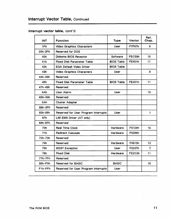
Interrupt Vector Table, Continued
Interrupt vector table, cont'd
Ref. INT Function Type Vector Chap.
1Fh Video Graphics Characters User F7F67h 9
20h-3Fh Reserved for DOS
40h Diskette BIOS Revector Software FEC59h 10
41h Fixed Disk Parameter Table BIOS Table FE401h 11
42h EGA Default Video Driver BIOS Table
43h Video Graphics Characters User 9
44h-45h Reserved
46h Fixed Disk Parameter Table BIOS Table FE401h 11
47h-49h Reserved
4Ah User Alarm User 15
4Bh-59h Reserved
5Ah Cluster Adapter
5Bh-5Fh Reserved
60h-66h Reserved for User Program Interrupts User 1
67h LIM EMS Driver (AT only)
68h-6Fh Reserved
70h Real Time Clock Hardware F5124h 15
71h Redirect Cascade Hardware F5266h
72h-73h Reserved
74h Reserved Hardware F4910h 13
75h 80287 Exception User F5257h 7
76h Fixed Disk Hardware FE2C3h 11
77h-7Fh Reserved
80h-FOh Reserved for BASIC BASIC 16
F1h-FFh Reserved for User Program Interrupts User
The ROM BIOS 11

Unexpected Interrupt Handler
O,scription
The BIOS initializes unused interrupt vectors to the BIOS unexpected interrupt handler routine. The unexpected interrupt handler processes all interrupts that are either special user processes (INT 1Ch or INT 4Ah), or not meaningful to the BIOS, such as INT 72h, 73h, or 74h, which are all reserved in PC, XT, and AT BlOSs.
Generally speaking the BIOS either ignores unexpected software interrupts, returning control to the interrupted program with registers preserved and the Carry Flag set or it revectors the interrupt to a caller-supplied routine. An example would be INT 1Ch, for which the caller would supply a routine that would access the BIOS INT 08h System Timer ISA.
An exception is INT ODh. If the microprocessor is an 80286, 80386SX, or 80386, the BIOS generates a screen message about a General Protection Fault.
continued
System BIOS for .IBM PC/XT I AT Computers and Compatibles 12

Unexpected Interrupt Handler, Continued
Interrupts initialized to BIOS unexpected interrupt handlers
The following interrupts are initialized by the BIOS to different unexpected interrupt handlers. Operating systems and user applications may replace these interrupt vectors, if they wish. The BIOS provides these routines to ensure complete BIOS error recovery.
INT Description
OOh Divide by zero
01h Single step
03h Breakpoint
04h Overflow
06h Invalid op code
07h Math coprocessor not present
OAh IRQ 2 Cascade from slave 8259A
OBh IRQ 3 Serial Communications hardware (COM2)
OCh IRQ 4 Serial Communications hardware (COM1)
ODh IRQ 5 Fixed disk controller
OFh Parallel printer IRQ 7
1Bh Keyboard Ctrl/Break
1Ch Timer tick
72h Reserved. IRQ 10
73h Reserved. IRQ 11
74h Reserved, IRQ 12
76h IRQ 14 Fixed disk controller
77h Reserved, IRQ 15
The ROM BIOS 13

System BIOS Functions and BIOS Diversity
Introduction
Throughout this manual, each ROM BIOS function description includes an explanation of what the function does, the function's required inputs and outputs, and any special programming considerations or hardware .. gotcha' s.. associated the the function.
Although all BlOSs in IBM-compatible microcomputers by definition have to be compatible with the IBM standard, there has been a tremendous amount of diversity in the level of functions supported between BIOS versions.
This diversity makes it difficult to precisely identify functions as PC-, XT -, or AT-specific. BIOS functions that are AT-only in IBM systems can be found in the Phoenix XT BIOS. And, depending on the manufacturer of the BIOS or computer, there are variations on which function appears in which XT or AT clone.
How to determine level of support
Throughout this book, the commonly accepted level of support for each ROM BIOS function is identified by the legend [PC], [XT] , and/or [AT] on the same line as the function title.
Legend Description
[PC] Function Is supported by the original IBM PC BIOS only.
[XT] Function is supported by all IBM PC/XT and compatible ROM BlOSs.
Note: This level of support Is contained In the ROM BIOS implemented in the majority of IBM PC and PC/XT compatible systems.
[AT] Function is supported by all IBM PCIAT and compatible ROM BlOSs.
continued
System BIOS for IBM PC/XT I AT Computers and Compatibles 14
System BIOS Functions and BIOS Diversity, Continued
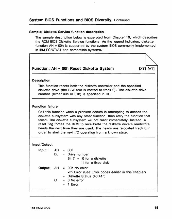
Sample: Diskette Service function description
The sample description below is excerpted from Chapter 10, which describes the ROM BIOS Diskette Service functions. As the legend indicates, diskette function AH = OOh is supported by the system BIOS commonly implemented in IBM PC/XT/AT and compatible systems.
Function: AH = OOh Reset Diskette System [XT] [AT]
Description
This function resets both the diskette controller and the specified diskette drive (the R/W arm is moved to track 0). The diskette drive number (either OOh or 01 h) is specified in DL.
Function failure
Call this function when a problem occurs in attempting to access the diskette subsystem with any other function, then retry the function that failed. The diskette subsystem will not react immediately. Instead, a reset flag forces the BIOS to recalibrate the diskette drive's read/write heads the next time they are used. The heads are relocated track 0 in order to start the next I/O operation from a known state.
Input/Output
Input: AH DL =
OOh Drive number Bit 7 = 0 for a diskette
1 for a fixed disk
Output: AH
CF = =
OOh No error xxh Error (See Error codes earlier in this chapter) Diskette Status (40:41 h) 0 No error
= 1 Error
The ROM BIOS 15
Video BIOS Functions and BIOS Diversity
Introduction
Since the introduction of the IBM PC in 1981, four video adapter types have emerged: MDA, CGA, EGA, and VGA. MDA and CGA adapters rely exclusively on the Video Service contained in the system board ROM BIOS of all PC/XT/AT and compatible computers. EGA and VGA adapters contain a dedicated ROM BIOS installed on the adapter hardware itself.
The number and sophistication of the functions supported by the video BlOSs associated with each adapter varies. As a general rule, the more recent the adapter, the greater the number of functions its BIOS supports.
Note: The Hercules display adapter allows for the display of 720x350 monochrome graphics on standard TTL monochrome monitors. However, neither the system ROM BIOS nor the Hercules adapter itself contain a BIOS. Applications programs that support Hercules graphics must contain an application-specific device driver.
How to determine level of support
When a function applies exclusively to the VGA adapter, for example, its description will bear the legend [VGA]. When the function applies to all adapter types, it will bear the legend [MDA] [CGA] [EGA] [VGA].
The table below describes the meaning of each legend.
Legend Description
[MDA] Function is supported by IBM Monochrome Display Adapters (MDA), and compatibles.
[CGA] Function is supported by IBM Color Graphics Adapter (CGA) , and compatibles.
[EGA] Function is supported by IBM Enhanced Graphics Adapter (EGA), and compatibles.
[VGA] Function is supported by IBM Video Graphics Array (VGA) and compatible adapters.
continued
System BIOS for IBM PC/XT/ AT Computers and Compatibles 16

Video BIOS Functions and BIOS Diversity, Continued
Sample: Video BIOS function description
The sample description below is excerpted from Chapter 9, which describes the BIOS Video Service functions. As the legend indicates, video function AH = 02h is supported by the video BIOS associated with MDA, CGA, EGA, and VGA adapters.
Function: AH = 02h Set Cursor Position [MDA] [eGA] [EGA] [VGA]
Description
The Set Cursor Position function sets the cursor position (in terms of row-by-column coordinates) for the display page indicated in BL. It saves the position as a two-byte row-by-column table entry in the cursor coordinates byte at 40:S0h. Rowand column coordinates are indicated in registers DH and DL respectively.
The Set Cursor Position function applies to both text and graphics video modes. In text modes, if the display page selected in BH is the active display page, the on-screen cursor will move to the coordinates indicated in registers DH and DL. In graphics modes, the cursor is invisible, but it is used to define a position on the screen.
Input/Output
Input: AH = 02h BH = Display page number (see function AH = aSh) DH = Row (0 is top row of screen) DL = Column (0 is leftmost column)
Output: AX = OOh
The ROM BIOS 17

Summary: The BIOS Services
Each BIOS service executes at least one function. When a BIOS service is capable of executing more than one function, functions are selected by placing the proper function number in the AH register. Subfunctions are selected via either the AL register or the BL register.
The tables below briefly define each BIOS service and list each BIOS function and subfunction.
Print Screen The BIOS Print Screen Service prints the contents Service of the current video screen to printer number O.
INT PARAMETER FUNCTION
OSh None Print Screen
The BIOS Video Service provides 1/0 support forVideo the MDA and eGA adapters. BIOS support for
Service EGA and VGA adapters is contained in adapter ROM.
INT PARAMETER FUNCTION
10h AH =OOh Set Video Mode
AH =01h Set Text Mode Cursor Size
AH =02h Set Cursor Position
AH =03h Read Current Cursor Position
AH =04h Read Light Pen Position
AH =OSh Select New Video Page
AH =06h Scroll Current Page Up
AH =07h Scroll Current Page Down
AH =08h Read CharacterlAttribute from Screen
AH =09h Write CharacterlAttribute to Screen
continued
System BIOS for IBM PC/XT/AT Computers and Compatibles 18

Summary: The BIOS Services, Continued
Video Service,
cont'd
INT PARAMETER
10h AH =OAh
AH =OBh
AH =OCh
AH =ODh
AH =OEh
AH =OFh
AH =10h
The BIOS Video Service provides 1/0 support for the MDA and eGA adapters. BIOS support for EGA and VGA adapters is contained in adapter ROM.
FUNCTION
Write Character Only to Screen
Set Color Palette
Write Pixel
Read Pixel
Write Teletype To Active Page
Return Video Status
Set Palette/Color Registers:
Parameter Subfunctlon
AL =OOh Set single palette AL =01h Set overscan register AL =02h Set all palette registers and overscan AL =03h Toggle intensify/blinking bit AL =04h-06h Reserved AL =07h Read individual palette register AL =08h Read overscan register (border color) AL =09h Read all palette registers and
overscan register (border color) AL = 10h Set Individual color register AL = 11h Reserved AL = 12h Set block of color registers AL = 13h Select color paging mode (not valid
for mode 13h) BL =OOh Select paging mode BL =01h Select page
AL = 14h Reserved AL = 15h Read single DAC c610r register AL = 16h Reserved AL = 17h Read block of color registers AL =18h-19h Reserved AL = 1Ah Read color paging status AL = 1Bh Sum color values to gray shades
continued
The ROM BIOS 19

Summary: The 810S Services, Continued
Video Service, cont'd
INT PARAMETER
10h AH =11h
10h AH =12h
Parameter
AL =OOh AL =01h AL =02h
AL =03h AL =04h AL = 10h
AL =11h
AL =12h
AL =14h
AL =20h
AL = 21h
AL = 22h AL = 23h
AL =24h AL =30h
Alternate Select:
Parameter
BL =10h BL =20h
BL =30h BL =31h
BL =32h BL =33h
BL =34h BL =35h BL =36h
The BIOS Video Service provides I/O support for MDA and CGA. BIOS support for EGA and VGA adapters is contained in adapter ROM.
FUNCTION
Load Character Generator:
Subfunctlon
Load user text mode font Load ROM 8x 14 text mode font Load ROM 8x8 double dot text mode font Set block specifier (text mode only)) Load 8x16 ROM text mode font Load user text mode font (after mode set) Load ROM 8x14 text mode font (after mode set) Load ROM 8x8 double dot text mode font (after mode set) Load 8x16 ROM text mode font (after mode set) Set user graphics characters pointer at INT 1 Fh (8x8 font) Set user graphics font pointer at INT 43h Use ROM 8x14 font for graphics Use ROM 8x8 double dot font for graphics ' Use ROM 8x16 font for graphics Get font pointer information
Subfunction
Return configuration Information Switch to alternate print screen routine Select scan lines for text modes Enable/disable default palette loading during set mode Enable/disable video Enable/disable summing to gray shades Enable/disable cursor scaling Switch display Video screen off/on
continued
System BIOS for IBM PC/XT/AT Computers and Compatibles 20

Summary: The BIOS Services, Continued
Video The BIOS Video Service provides I/O support for Service, the MDA and CGA adapters. BIOS support for EGA
cont'd and VGA adapters is contained in adapter ROM.
INT PARAMETER FUNCTION
10h AH =13h Write String:
Parameter Subfunctlon
AL =OOh Cursor not moved AL =01h Cursor Is moved AL =02h Cursor not moved (text modes only) AL =03h Cursor Is moved (text modes only)
AH =14h-19h Reserved
AH = lAh Read/Write Display Combination Code:
Parameter Subfunction
AL =OOh Read display combination code AL =01h Write display combination code
AH = lBh Return Functionality/State Information
AH = lCh Save/Restore Video State
AH = lDh-FFh Reserved
The BIOS Equipment List Service returns the Equipment List system equipment list, as determined by the BIOSService POST routine.
INT PARAMETER FUNCTION
llh None Read Equipment List
continued
The ROM BIOS 21

Summary: The BIOS Services, Continued
Memory Size Service
INT PARAMETER
12h None
Diskette Service
INT PARAMETER
13h AH =OOh
AH =01h
AH = 02h
AH =03h
AH =04h
AH =OSh
AH = 06h-07h
AH = 08h
AH = 09h-14h
AH =1Sh
AH =16h
AH =17h
AH =18h
AH =19h-FFh
The BIOS Memory Size Service returns the amount of available base memory (in Kilobytes). as determined by the POST routine.
FUNCTION
Read Memory Size
The BIOS Diskette Service performs BIOS-level read. write. format. initialization, and diagnostic support for up to two internal diskette drives.
Note: If a fixed disk is installed. the BIOS automatically revectors all 13h Diskette Service requests to INT 40h. Revectoring is transparent to end users. End users should continue to use INT 13h for both fixed disk and diskette service requests.
FUNCTION
Reset Diskette System
Read Diskette Status
Read Diskette Sectors
Write Diskette Sectors
Verify Diskette Sectors
Format Diskette Track
Reserved
Read Drive Parameters
Reserved
Read Drive Type
Detect Media Change
Set Diskette Type
Set Media Type for Format
Reserved
continued
System BIOS for IBM PC/XT I AT Computers and Compatibles 22

Summary: The BIOS Services, Continued
Fixed Disk Service
INT PARAMETER
13h AH =OOh
AH =01h
AH =02h
AH =03h
AH =04h
AH =OSh
AH =06h
AH =07h
AH =08h
AH =09h
AH =OAh
AH =OBh
AH =OCh
AH =ODh
AH =OEh
AH =OFh
AH =10h
AH =11h
AH =12h
AH =13h
AH =14h
AH =1Sh
AH =16h-FFh
The BIOS Fixed Disk Service performs BIOS level read, write, format, initialization, and diagnostic functions for up to two fixed disk drives.
FUNCTION
Reset Dlskette(s) and Fixed Disk
Read Fixed Disk Status
Read Sectors
Write Sectors
Verify Sectors
Format Cylinder
Format Bad Track
Format Drive
Read Drive Parameters
Initialize Drive Parameters
Read Long Sectors
Write Long Sectors
Seek to Cylinder
Alternate Fixed Disk Reset
Diagnostics 1: Read Test Buffer
Diagnostics 2: Write Test Buffer
Test for Drive Ready
Recalibrate Drive
Controller RAM Diagnostic
Controller Drive Diagnostic
Controller Internal Diagnostic
Read Fixed Disk Type
Reserved
continued
The ROM BIOS 23
Summary: The BIOS Services, Continued
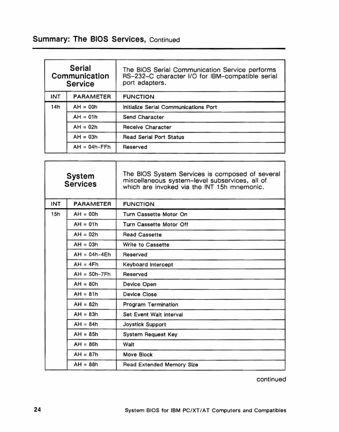
Serial Communication
Service
INT PARAMETER
14h AH = OOh
AH = 01h
AH =02h
AH = 03h
AH =04h-FFh
System Services
INT PARAMETER
15h AH = OOh
AH =01h
AH = 02h
AH =03h
AH =04h-4Eh
AH =4Fh
AH = 50h-7Fh
AH = 80h
AH =81h
AH =82h
AH =83h
AH =84h
AH =85h
AH =86h
AH = 87h
AH =aah
The BIOS Serial Communication Service performs RS-232-C character 110 for IBM-compatible serial port adapters.
FUNCTION
Initialize Serial Communications Port
Send Character
Receive Character
Read Serial Port Status
Reserved
The BIOS System Services is composed of several miscellaneous system-level subservices, all of which are invoked via the INT 15h mnemonic.
FUNCTION
Turn Cassette Motor On
Turn Cassette Motor Off
Read Cassette
Write to Cassette
Reserved
Keyboard Intercept
Reserved
Device Open
Device Close
Program Termination
Set Event Wait Interval
Joystick Support
System Request Key
Wait
Move Block
Read Extended Memory Size
continued
System BIOS for IBM PC/XT /AT Computers and Compatibles 24
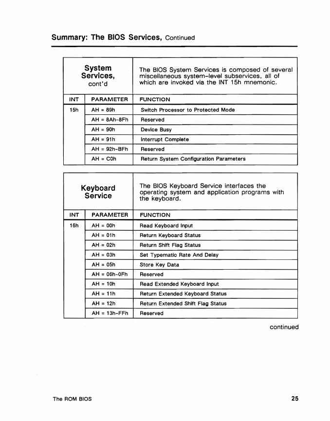
Summary: The BIOS Services, Continued
System Services,
cont'd
INT PARAMETER
1Sh AH = 89h
AH = 8Ah-8Fh
AH = 90h
AH = 91h
AH = 92h-BFh
AH = COh
Keyboard Service
INT PARAMETER
16h AH = OOh
AH = 01h
AH= 02h
AH = 03h
AH = OSh
AH = 06h-OFh
AH = 10h
AH = 11h
AH = 12h
AH = 13h-FFh
The BIOS System Services is composed of several miscellaneous system-level subservices, all of which are invoked via the INT 15h mnemonic.
FUNCTION
Switch Processor to Protected Mode
Reserved
Device Busy
Interrupt Complete
Reserved
Return System Configuration Parameters
The BIOS Keyboard Service interfaces the operating system and application programs with the keyboard.
FUNCTION
Read Keyboard Input
Return Keyboard Status
Return Shift Flag Status
Set Typematic Rate And Delay
Store Key Data
Reserved
Read Extended Keyboard Input
Return Extended Keyboard Status
Return Extended Shift Flag Status
Reserved
continued
The ROM BIOS 25
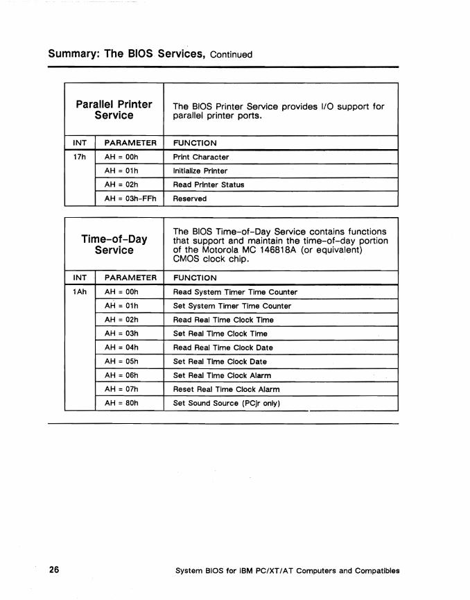
Summary: The BIOS Services, Continued
Parallel Printer Service
INT PARAMETER
17h AH =OOh
AH =01h
AH =02h
AH =03h-FFh
Time-of-Day Service
INT PARAMETER
1Ah AH =OOh
AH =01h
AH =02h
AH =03h
AH =04h
AH =05h
AH =OSh
AH =07h
AH =BOh
The BIOS Printer Service provides 1/0 support for parallel printer ports.
FUNCTION
Print Character
Initialize Printer
Read Printer Status
Reserved
The BIOS Time-of-Day Service contains functions that support and maintain the time-of-day portion of the Motorola MC 146818A (or equivalent) CMOS clock chip.
FUNCTION
Read System Timer Time Counter
Set System Timer Time Counter
Read Real Time Clock Time
Set Real Time Clock Time
Read Real Time Clock Date
Set Real Time Clock Date
Set Real Time Clock Alarm
Reset Real Time Clock Alarm
Set Sound Source (PC]r only)
System BIOS for IBM PC/XT I A T Computers and Compatibles 26
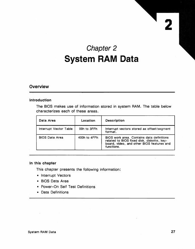
Chapter 2
System RAM Data
Overview
Introduction
The BIOS makes use of information stored in system RAM. The table below characterizes each of these areas.
Data Area Location
Interrupt Vector Table OOh to 3FFh
BIOS Data Area 400h to 4FFh
In this chapter
Description
Interrupt vectors stored as offset/segment format.
BiOS work area. Contains data definitions related to BIOS fixed disk. diskette. keyboard. video. and other BIOS features and functions.
This chapter presents the following information:
• Interrupt Vectors
• BIOS Data Area
• Power-On Self Test Definitions
• Data Definitions
System RAM Data 27
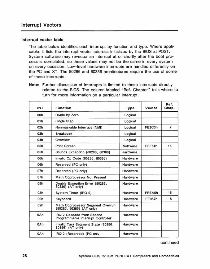
Interrupt Vectors
Interrupt vector table
The table below identifies each interrupt by function and type. Where applicable, it lists the interrupt vector address initialized by the BIOS at POST. System software may revector an interrupt at or shortly after the boot process is completed, so these values may not be the same in every system on every occasion. Low-level hardware interrupts are handled differently on the PC and XT. The 80286 and 80386 architectures require the use of some of these interrupts.
Note: Further discussion of interrupts is limited to those interrupts directly related to the BIOS. The column labeled "Ref. Chapter" tells where to turn for more information on a particular interrupt.
Ref. INT Function Type Vector Chap.
OOh Divide by Zero Logical
01h Single Step Logical
02h Nonmaskable Interrupt (NMI) Logical FE2C3h 7
03h Breakpoint Logical
04h Overflow Logical
OSh Print Screen Software FFFS4h 16
OSh Bounds Exception (80286, 80386) Hardware
06h Invalid Op Code (80286. 80386) Hardware
06h Reserved (PC only) Hardware
07h Reserved (PC only) Hardware
07h Math Coprocessor Not Present Hardware
08h Double Exception Error (80286, Hardware 80386) (AT only)
08h System Timer (IRQ 0) Hardware FFEASh 15
09h Keyboard Hardware FE987h 8
09h Math Coprocessor Segment Overrun Hardware (80286, 80386) (AT only)
OAh IRQ 2 Cascade from Second Hardware Programmable Interrupt Controller
OAh Invalid Task Segment State (80286, Hardware 80386) (AT only)
OAh IRQ 2 (Reserved) (PC only) Hardware
continued
28 System BIOS for IBM PC/XT I A T Computers and Compatibles
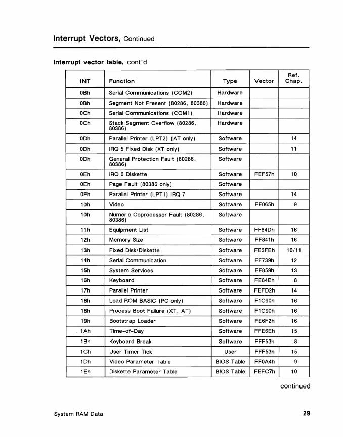
Interrupt Vectors, Continued
Interrupt vector table, cont'd
Ref. INT Function Type Vector Chap.
OBh Serial Communications (COM2) Hardware
OBh Segment Not Present (80286, 80386) Hardware
OCh Serial Communications (COM1) Hardware
OCh Stack Segment Overflow (80286. Hardware 80386)
ODh Parallel Printer (LPT2) (AT only) Software 14
ODh IRQ 5 Fixed Disk (XT only) Software 11
ODh General Protection Fault (80286, Software 80386)
OEh IRQ 6 Diskette Software FEF57h 10
OEh Page Fault (80386 only) Software
OFh Parallel Printer (LPT1) IRQ 7 Software 14
10h Video Software FF065h 9
10h Numeric Coprocessor Fault (80286, 80386)
Software
11 h Equipment List Software FF84Dh 16
12h Memory Size Software FF841h 16
13h Fixed DisklDiskette Software FE3FEh 10/11
14h Serial Communication Software FE739h 12
15h System Services Software FF859h 13
16h Keyboard Software FE84Eh 8
17h Parallel Printer Software FEFD2h 14
18h Load ROM BASIC (PC only) Software F1C90h 16
18h Process Boot Failure (XT, AT) Software F1C90h 16
19h Bootstrap Loader Software FE6F2h 16
1Ah Time-of-Day Software FFE6Eh 15
1Bh Keyboard Break Software FFF53h 8
1Ch User Timer Tick User FFF53h 15
1Dh Video Parameter Table BIOS Table FFOA4h 9
1Eh Diskette Parameter Table BIOS Table FEFC7h 10
continued
System RAM Data 29

Interrupt Vectors, Continued
Interrupt vector table, cont'd
Ref. INT Funqtlon Type Vector Chap.
1Fh Video Graphics Characters User F7F67h 9
20h-3Fh Reserved for DOS
40h Diskette BIOS Revector Software FEC59h 10
41h Fixed Disk Parameter Table BIOS Table FE401h 11
42h EGA Default Video Driver BIOS Table
43h Video Graphics Characters User 9
44h-45h Reserved
46h Fixed Disk Parameter Table BIOS Table FE401h 11
47h-49h Reserved
4Ah User Alarm User 15
4Bh-59h Reserved
5Ah Cluster Adapter
5Bh-5Fh Reserved
60h-66h Reserved for User Program Interrupts User 1
67h LIM EMS Driver (AT only)
68h-6Fh Reserved
70h Real Time Clock Hardware F5124h 15
71h Redirect Cascade Hardware F5266h
72h-73h Reserved
74h Reserved Hardware F4910h 13
75h 80287 Exception User F5257h 7
76h Fixed Disk Hardware FE2C3h 11
77h-7Fh Reserved
80h-FOh Reserved for BASIC BASIC 16
F1h-FFh Reserved for User Program Interrupts User
. System BIOS for IBM PC/XTI AT Computers and Compatibles 30
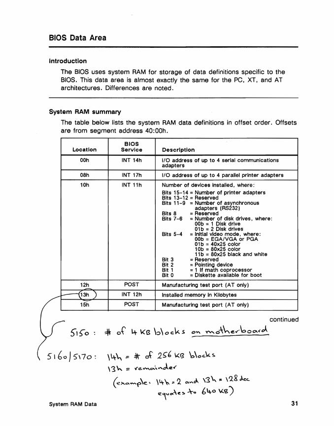
BIOS Data Area
Introduction
The BIOS uses system RAM for storage of data definitions specific to the BIOS. This data area is almost exactly the same for the PC, XT, and AT architectures. Differences are noted.
System RAM summary
The table below lists the system RAM data definitions in offset order. Offsets are from segment address 40:00h.
BIOS Location Service Description
OOh INT 14h 1/0 address of up to 4 serial communications adapters
08h INT 17h 1/0 address of up to 4 parallel printer adapters
10h INT 11 h Number of devices Installed, where: Bits 15-14 = Number of printer adapters Bits 13-12 = Reserved Bits 11-9 = Number of asynchronous
adapters (RS232) Bits 8 = Reserved Bits 7-6 = Number of disk drives, where:
OOb = 1 Disk drive 01b = 2 Disk drives
Bits 5-4 = Initial video mode, where: OOb = EGAIVGA or PGA 01b = 40x25 color 1Db = 80x25 color 11 b = 80x25 black and white
Bit 3 = Reserved Bit 2 = Pointing device Bit 1 =1 If math coprocessor Bit 0 =Diskette available for boot
12h POST Manufacturing test port (AT only)
INT 12h Installed memory In Kilobytes(~3h) 15h POST Manufacturing test port (AT only)
continued
~ 0.(' 4 \«3 \~\ock$ 't'¥., 0-\"'. e.r\0 0 0\" cA5'1~o . 0'"'
51bo 5\70 : ::: ~ cl 2~b \«3 'b\ocks.\4-'" , '3 h. = '"e "",.,.:, ",J,.e or
!' \ \1. \ __ 1"1 - ..... ck \'5 '" = \ 28 eke.. \.. <::>-."" ....... f"e.. ..,. ~ "'
€,""'-\c," -\-0 6'+0~«) System RAM Data 31
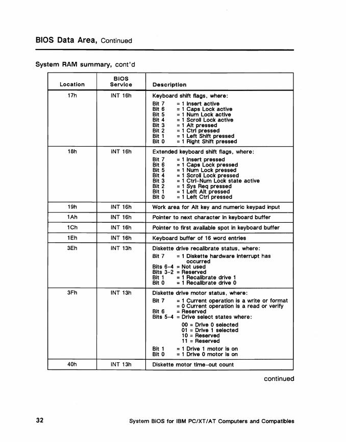
BIOS Data Area, Continued
System RAM summary. cont'd
BIOS Location Service
17h INT 16h
18h INT 16h
19h INT 16h
1Ah INT 16h
1Ch INT 16h
1Eh INT 16h
3Eh INT 13h
3Fh INT 13h
40h INT 13h
Description
Keyboard shift flags. where: Bit 7 =1 Insert active Bit 6 =1 Caps Lock active Bit 5 =1 Num Lock active Bit 4 =1 Scroll Lock active Bit 3 =1 Alt pressed Bit 2 =1 Ctrl pressed Bit 1 = 1 Left Shift pressed Bit 0 =1 Right Shift pressed
Extended keyboard shift flags. where: Bit 7 =1 Insert pressed Bit 6 = 1 Caps Lock pressed Bit 5 =1 Num Lock pressed Bit 4 =1 Scroll Lock pressed Bit 3 =1 Ctrl-Num Lock state active Bit 2 =1 Sys Req pressed Bit 1 =1 Left Alt pressed Bit 0 =1 Left Ctrl pressed
Work area for Alt key and numeric keypad input
Pointer to next character In keyboard buffer
Pointer to first available spot In keyboard buffer
Keyboard buffer of 16 word entries
Diskette drive recallbrate status. where: Bit 7 =1 Diskette hardware Interrupt has
occurred Bits 6-4 =Not used Bits 3-2 =Reserved Bit 1 =1 Recallbrate drive 1 Bit 0 =1 Recallbrate drive 0
Diskette drive motor status. where: Bit 7 =1 Current operation Is a write or format
=0 Current operation Is a read or verify Bit 6 =Reserved Bits 5-4 =Drive select states where:
00 =Drive 0 selected 01 =Drive 1 selected 1 0 =Reserved 11 =Reserved
Bit 1 =1 Drive 1 motor Is on Bit 0 =1 Drive 0 motor Is on
Diskette motor time-out count
continued
System BIOS for IBM PC/XT/AT Computers and Compatibles 32
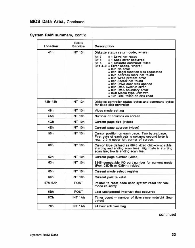
BIOS Data Area, Continued
System RAM summary, cont'd
BIOS Location Service
41h INT 13h
42h-48h INT 13h
49h INT 10h
4Ah INT 10h
4Ch INT 10h
4Eh INT 10h
50h INT 10h
60h INT 10h
62h INT 10h
63h INT 10h
65h INT 10h
66h INT 10h
67h-6Ah POST
6Bh POST
6Ch INT 1Ah
70h INT 1Ah
Description
Diskette status return code, where:
Bit 7 =1 Drive not ready Bit 6 =1 Seek error occurred Bit 5 =1 Diskette controller failed Bits 4-0 =Error codes, where:
=OOh No error =01 h Illegal function was requested =02h Address mark not found =03h Write protect error =04h Sector not found =06h Drive door was opened =OSh DMA overrun error =09h DMA boundary error =OCh Media type unknown =10h CRC failed on disk read
Diskette controller status bytes and command bytes for fixed disk controller
Video mode setting
Number of columns on screen
Current page size (video)
Current page address (video)
Cursor position on each page. Two bytes/page. First byte of each pair is column; second byte is row. 0,0 is upper left corner of screen.
Cursor type defined as 6845 video chip-compatible starting and ending scan lines. High byte is starting scan line; low Is ending scan line.
Current page number (video)
6845-compatlble I/O port number for current mode (Port 03D4h or 03B4h) (video)
Current mode select register
Current palette value
Pointer to reset code upon system reset for real mode re-entry
Last unexpected Interrupt that occurred
Timer count - number of ticks since midnight (four bytes)
24 hour roll over flag
continued
System RAM Data 33

BIOS Data Area, Continued
System RAM summary, cont'd
BIOS Location Service
71h INT 16h
72h POST
74h INT 13h
7Sh iNT 13h
76h INT 13h
77h INT 17h
78h INT 14h
7Ch INT 16h
80h INT 16h
82h INT 10h
84h INT 10h
85h INT 10h
Description
Ctrl-Break flag (bit 7 = 1 <CtrI><Break> pressed)
System Reset Flag (AT only). where:
1234h =Bypass memory test (also warm boot) 4321 h =Preserve memory 64h =Burn In mode
Status from last fixed disk operation. where:
OOh =No error 01h = Invalid function request 02h =Address mark not found 03h =Write protect error 04h =Sector not found OSh =Reset failed 07h =Drive parameter activity failed OBh =DMA overrun on operation 09h =Data boundary error OAh =Bad sector flag detected OBh =Bad track detected ODh =Invalid number of sectors on format OEh =Control data address mark detected OFh =DMA arbitration level out of range 10h =Uncorrectable ECC or CRC error 11 h =ECC corrected data error 20h =General controller failure 40h =Seek operation failed -BOh =Time-out AAh =Drive not ready BBh =Undefined error occurred CCh =Write fault on selected drive EOh =Status error/error register is 0 FFh =Sense operation failed
Number of fixed disks
Fixed disk control byte
Fixed disk port offset
Printer time-out table (ports 0-3)
Serial time-out table (ports 0-3)
Offset to start of keyboard buffer (from segment 40h)
Offset to end of keyboard buffer (from segment 40h)
Number of rows on screen (24/2S) (VGA only)
Character height (bytes/character) (VGA only)
continued
System BIOS for IBM PC/XT / AT Computers and C0!'T1patibles 34
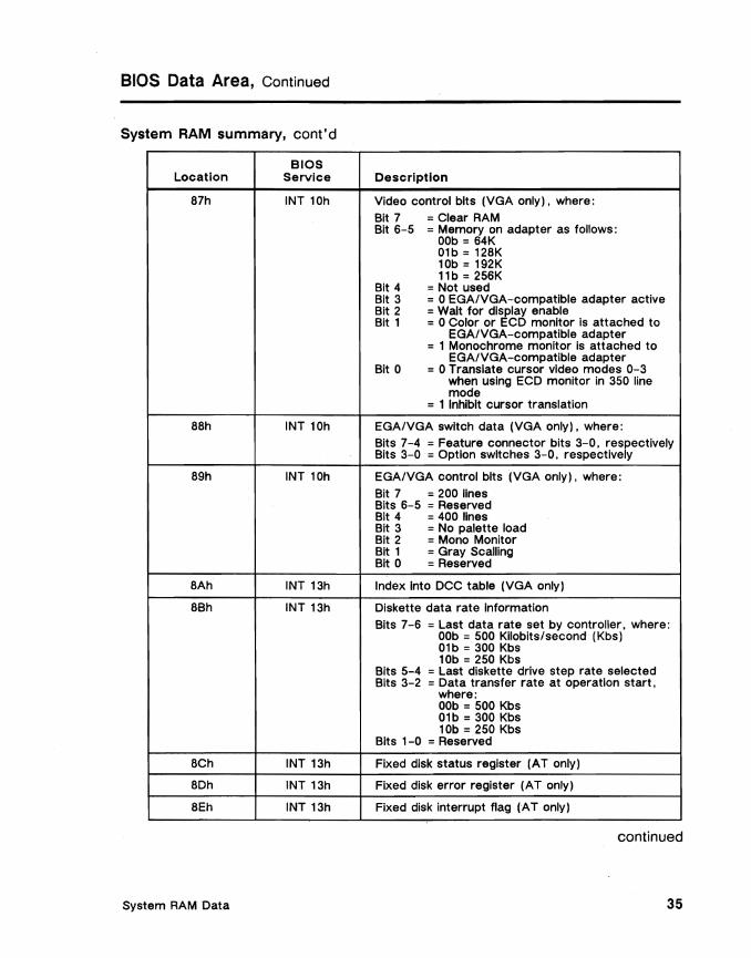
BIOS Data Area, Continued
System RAM summary, cont'd
BIOS Location Service
87h INT 10h
88h INT 10h
89h INT 10h
8Ah INT 13h
8Sh INT 13h
BCh INT 13h
BDh INT 13h
BEh INT 13h
Oescrl.ptlon
Video control bits (VGA only). where: Bit 7 = Clear RAM Bit 6-5 =Memory on adapter as follows:
OOb =64K 01b = 128K 10b = 192K 11b =256K
Bit 4 = Not used Bit 3 =0 EGAIVGA-compatible adapter active Bit 2 =Walt for display enable Bit 1 =0 Color or ECD monitor Is attached to
EGAIVGA-compatible adapter =1 Monochrome monitor is attached to
EGAIVGA-compatible adapter Bit 0 =0 Translate cursor video modes 0-3
when using ECD monitor In 350 line mode
= 1 Inhibit cursor translation
EGAIVGA switch data (VGA only). where: Bits 7-4 = Feature connector bits 3-0. respectively Bits 3-0= Option switches 3-0, respectively
EGAIVGA control bits (VGA only), where:
Bit 7 =200 lines Bits 6-5 = Reserved Bit 4 =400 lines Bit 3 =No palette load Bit 2 =Mono Monitor Bit 1 =Gray Scalling Bit 0 =Reserved
Index Into DeC table (VGA only)
Diskette data rate Information Bits 7-6 =Last data rate set by controller. where:
OOb =500 Kllobits/second (Kbs) 01b =300 Kbs 10b =250 Kbs
Bits 5-4 =Last diskette drive step rate selected Bits 3-2 =Data transfer rate at operation start.
where: OOb =500 Kbs 01b =300 Kbs 10b =250 Kbs
Bits 1-0 =Reserved
Fixed disk status register (AT only)
Fixed disk error register (AT only)
Fixed disk interrupt flag (AT only)
continued
System RAM Data 35
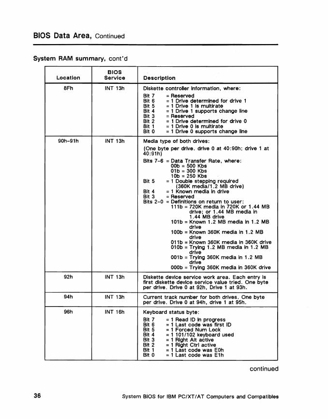
BIOS Data Area, Continued
System RAM summary, cont'd
BIOS Location Service
8Fh INT 13h
90h-91h INT 13h
92h INT 13h
94h INT 13h
96h INT 16h
40:91h) Bits 7-6
Bit 5
Bit 4 Bit 3 Bits 2-0
Description
Diskette controller Information. where: Bit 7 =Reserved Bit 6 =1 Drive determined for drive 1 Bit 5 =1 Drive 1 Is multirate Bit 4 =1 Drive 1 supports change line Bit 3 =Reserved Bit 2 =1 Drive determined for drive 0 Bit 1 =1 Drive 0 Is multirate Bit 0 = 1 Drive 0 supports change line
Media type of both drives: (One byte per drive. drive 0 at 40:90h; drive 1 at
=Data Transfer Rate. where: OOb =500 Kbs 01b =300 Kbs 10b =250 Kbs
=1 Double stepping required (360K media/1.2 MB drive)
=1 Known media In drive =Reserved =Definitions on return to user:
111b =720K media In 720K or 1.44 MB drive; or 1.44 MB media in 1.44 MB drive
101b =Known 1.2 MB media In 1.2 MB drive
100b =Known 360K media in 1.2 MB drive
011 b =Known 360K media In 360K drive 010b =Trying 1.2 MB media in 1.2 MB
drive 001b =Trying 360K media in 1.2 MB
drive OOOb =Trying 360K media in 360K drive
Diskette device service work area. Each entry Is first diskette device service value tried. One byte per drive. Drive 0 at 92h. Drive 1 at 93h.
Current track number for both drives. One byte per drive. Drive 0 at 94h. drive 1 at 95h.
Keyboard status byte: Bit 7 Bit 6 Bit 5 Bit 4 Bit 3 Bit 2 Bit 1 Bit 0
=1 Read 10 In progress =1 Last code was first 10 =1 Forced Num Lock =1 101/102 keyboard used =1 Right Alt active =1 Right Ctrl active =1 Last code was EOh =1 Last code was E1h
continued
System BIOS for IBM PC/XT 1 AT Computers and Compatibles 36
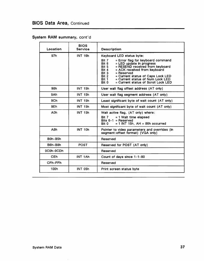
BIOS Data Area, Continued
System RAM summary, cont'd
Location
97h
98h
9Ah
9Ch
9Eh
AOh
A8h
BOh-B5h
B6h-B8h
OCOh-OCDh
CEh
CFh-FFh
100h
BIOS Service
INT 16h
INT 15h
INT 15h
INT 15h
INT 15h
INT 15h
INT 10h
POST
INT 1Ah
INT 05h
Description
Keyboard LED status byte: Bit 7 =Error flag for keyboard command Bit 6 =LED update In progress Bit 5 =RESEND received from keyboard Bit 4 =ACK received from keyboard Bit 3 =Reserved Bit 2 =Current status of Caps Lock LED Bit 1 =Current status of Num Lock LED Bit 0 =Current status of Scroll Lock LED
User walt flag offset address (AT only)
User wait flag segment address (AT only)
Least significant byte of walt count (AT only)
Most significant byte of wait count (AT only)
Walt active flag, (AT only) where: Bit 7 =1 Wait time elapsed Bits 6-1 =Reserved Bit 0 =1 INT 15h, AH =86h occurred
Pointer to video parameters and overrides (In segment:offset format) (VGA only)
Reserved
Reserved for POST (AT only)
Reserved
Count of days since 1-1-80
Reserved
Print screen status byte
System RAM Data 37
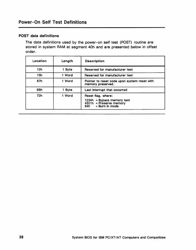
Power-On Self Test Definitions
POST data definitions
The data definitions used by the power-on self test (POST) routine are stored in system RAM at segment 40h and are presented below in offset order.
Location Length Description
12h 1 Byte Reserved for manufacturer test
15h 1 Word Reserved for manufacturer test
67h 1 Word Pointer to reset code upon system reset with memory preserved.
6Bh 1 Byte Last interrupt that occurred
72h 1 Word Reset flag. where: 1234h =Bypass memory test 4321h =Preserve memory 64h =Burn in mode
System BIOS for IBM PC/XT / AT Computers and Compatibles 38

INT 10h Video Service Data Definitions
Video data definitions
The data definitions used by the INT 10h. Video Service. are stored in system RAM in segment 40h and are presented below in offset order.
Location Length
10h 1 Byte
49h 1 Byte
4Ah 1 Word
4Ch 1 Word
4Eh 1 Word
SOh 8 Words
60h 1 Word
62h 1 Byte
63h 1 Word
65h 1 Byte
66h 1 Byte
84h 1 Byte
85h 1 Word
Description
Number of devices Installed. where: Bits 15-14 =Number of printer adapters Bits 13-12 =Reserved Bits 11-9 =Number of asynchronous
adapters (RS232) Bits 8 =Reserved Bits 7-6 =Number of disk drives. where:
OOb =1 Disk drive 01 b =2 Disk drives
Bits 5-4 =Initial video mode. where: OOb =EGAIVGA or PGA 01b =40x25 color 10b =80x25 color 11 b =80x25 black and white
Bit 3 =Reserved Bit 2 =Pointing device Bit 1 =1 If math coprocessor Bit 0 =Diskette available for boot
Video mode setting.
Number of columns on screen (40 or 80).
Current page size (In bytes).
Offset of current page address.
Cursor position on each page. Two bytes/page. First byte (low order) of each pair is column. second is row. 0.0 Is the upper left corner of screen.
Cursor type defined as 6845-compatible starting and ending scan lines. High-order byte holds starting scan line; low-order byte holds ending scan line.
Current page number.
6845-compatible 110 port number for current mode. where: 03B4h =Monochrome 03D4h =Color
Current mode select register.
Current palette value.
Number of rows on screen minus one (24 or 25)
Character height (bytes/character)
continued
System RAM Data 39
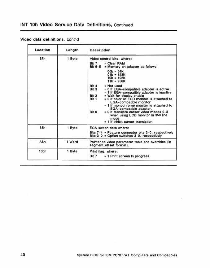
INT 10h Video Service Data Definitions, Continued
Video data definitions, cont'd
Location Length
87h 1 Byte
88h 1 Byte
A8h 1 Word
100h 1 Byte
Description
Video control bits. where: Bit 7 =Clear RAM Bit 6-5 =Memory on adapter as follows:
OOb = 64K 01b = 128K 10b =192K 11b = 256K
Bit 4 =Not used Bit 3 =0 If EGA-compatible adapter is active
=1 If EGA-compatible adapter is inactive Bit 2 =Wait for display enable Bit 1 =0 If color or ECD monitor is attached to
EGA-compatible monitor =1 If monochrome monitor is attached to
EGA-compatible adapter. Bit 0 =0 If translate cursor video modes 0-3
when using ECD monitor in 350 line mode
=1 If inhibit cursor translation
EGA switch data where: Bits 7-4 = Feature connector bits 3-0. respectively Bits 3-0 =Option switches 3-0. respectively
Pointer to video parameter table and overrides (In segment:offset format).
Print flag. where: Bit 7 = 1 Print screen In progress
System BiOS for IBM PC/XTI A T Computers and Compatibles 40
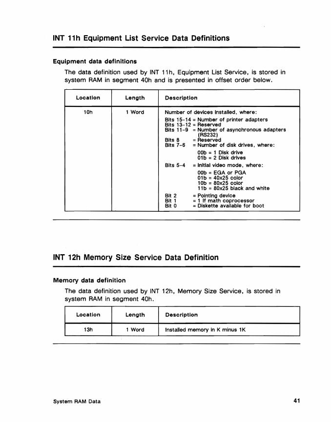
INT 11h Equipment List Service Data Definitions
Equipment data definitions
The data definition used by INT 11 h. Equipment List Service. is stored in .system RAM in segment 40h and is presented in offset order below.
Location Length Description
10h 1 Word Number of devices Installed, where: Bits 15-14 =Number of printer adapters Bits 13-12 =Reserved Bits 11-9
Bits 8
=Number of asynchronous adapters (RS232)
=Reserved Bits 7-6 =Number of disk drives, where:
OOb =1 Disk drive 01 b =2 Disk drives
Bits 5-4 =Initial video mode, where: OOb =EGA or PGA 01b =40x25 color 10b =80x25 color 11 b =80x25 black and white
Bit 2 Bit 1 Bit 0
=Pointing device =1 If math coprocessor =Diskette available for boot
INT 12h Memory Size Service Data Definition
Memory data definition
The data definition used by INT 12h, Memory Size Service. is stored in system RAM in segment 40h.
Location Length Description
13h 1 Word Installed memory In K minus 1 K
System RAM Data 41

INT 13h Diskette Service Data Definitions
Diskette data definitions
The data definitions used by INT 13h, Diskette Service, are stored in system RAM in segment 40h and are presented below in offset order.
Location Length Description
3Eh 1 Byte Diskette drive recallbrate status, where: Bit 7 =1 Diskette hardware Interrupt has
occurred Bits 6-4 =Not used Bits 3-2 =Reserved Bit 1 =1 Recalibrate drive 1 Bit 0 =1 Recallbrate drive 0
3Fh 1 Byte Diskette motor status, where:
Bit 7 =1 Current operation is a write or format =0 Current operation Is a read or verify
Bit 6 =Reserved Bit 5-4 =Drive select states where:
00 =Drive 0 selected 01 =Drive 1 selected 10 =Reserved 11 =Reserved
Bit 1 =1 Drive 1 motor is on Bit 0 = 1 Drive 0 motor is on
40h 1 Byte Diskette motor time-out count
41h 1 Byte Diskette status return code, where: Bit 7 =1 Drive not ready Bit 6 = 1 Seek error occurred Bit 5 = 1 Diskette controller failed Bits 4-0 =Error codes, where:
=01 h Illegal function was requested = 02h Address mark not found =03h Write protect error =04h Sector not found = 06h Drive door was opened =08h DMA overrun error =09h DMA boundary error =OCH Media type unknown =10h CRC failed on disk read
continued
System BIOS for IBM PC/XT/AT Computers and Compatibles 42
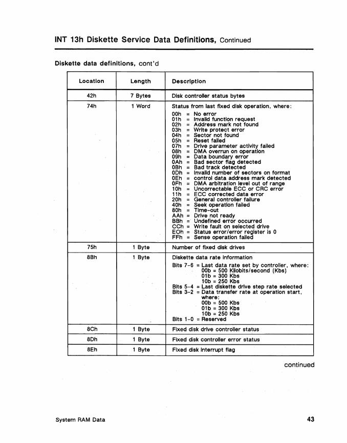
INT 13h Diskette Service Data Definitions, Continued
Diskette data definitions, cont'd
Location Length
42h 7 Bytes
74h 1 Word
75h 1 Byte
8Bh 1 Byte
8Ch 1 Byte
8Dh 1 Byte
8Eh 1 Byte
Description
Disk controller status bytes
Status from last fixed disk operation, where:
OOh = No error 01h = Invalid function request 02h = Address mark not found 03h = Write protect error 04h = Sector not found 05h = Reset failed 07h = Drive parameter activity failed 08h = DMA overrun on operation 09h = Data boundary error OAh = Bad sector flag detected OBh = Bad track detected ODh = Invalid number of sectors on format OEh = control data address mark detected OFh = DMA arbitration level out of range 10h = Uncorrectable ECC or CRC error 11h = ECC corrected data error 20h = General controller failure 40h = Seek operation failed 80h = Time-out AAh = Drive not ready BBh = Undefined error occurred CCh = Write fault on selected drive EOh = Status error/error register is 0 FFh = Sense operation failed
Number of fixed disk drives
Diskette data rate information Bits 7-6 =Last data rate set by controller, where:
OOb =500 Kliobits/second (Kbs) 01b =300 Kbs 10b =250 Kbs
Bits 5-4 =Last diskette drive step rate selected Bits 3-2 =Data transfer rate at operation start,
where: OOb =500 Kbs 01b =300 Kbs 10b =250 Kbs
Bits 1-0 =Reserved
Fixed disk drive controller status
Fixed disk controller error status
Fixed disk Interrupt flag
continued
System RAM Data 43
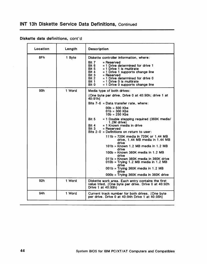
INT 13h Diskette Service Data Definitions, Continued
Diskette data definitions, cont'd
Location Length Description
8Fh 1 Byte Diskette controller Information, where: Bit 7 Bit 6 Bit 5 Bit 4 Bit 3 Bit 2 Bit 1 Bit 0
=Reserved =1 Drive determined for drive 1 =1 Drive 1 Is multlrate =1 Drive 1 supports change line =Reserved =1 Drive determined for drive 0 =1 Drive 0 Is multlrate =1 Drive 0 supports change line
90h 1 Word Media type of both drives: (One byte per drive. Drive 0 at 40:90h; drive 1 at 40:91h) Bits 7-6
Bit 5
Bit 4 Bit 3 Bits 2-0
=Data transfer rate, where: OOb =500 Kbs 01b =300 Kbs 10b =250 Kbs
=1 Double stepping required (360K medial 1.2M drive)
=1 Known media in drive =Reserved =Definitions on return to user:
111b = 720K media In 720K or 1.44 MB drive, 1.44 MB media In 1.44 MB drive
101b = Known 1.2 MB media In 1.2 MB drive
100b =Known 360K media in 1.2 MB drive
011 b =Known 360K media In 360K drive 010b =Trying 1.2 MB media in 1.2 MB
drive 001b =Trying 360K media in 1.2 MB
drive OOOb = Trying 360K media In 360K drive
92h 1 Word Diskette work area. Each entry contains the first value tried. (One byte per drive. Drive 0 at 40:92h Drive 1 at 40:93h)
94h 1 Word Current track number for both drives. (One byte per drive. Drive 0 at 40:94h Drive 1 at 40:95h)
System BIOS for IBM PC/XT I A T Computers and Compatibles 44
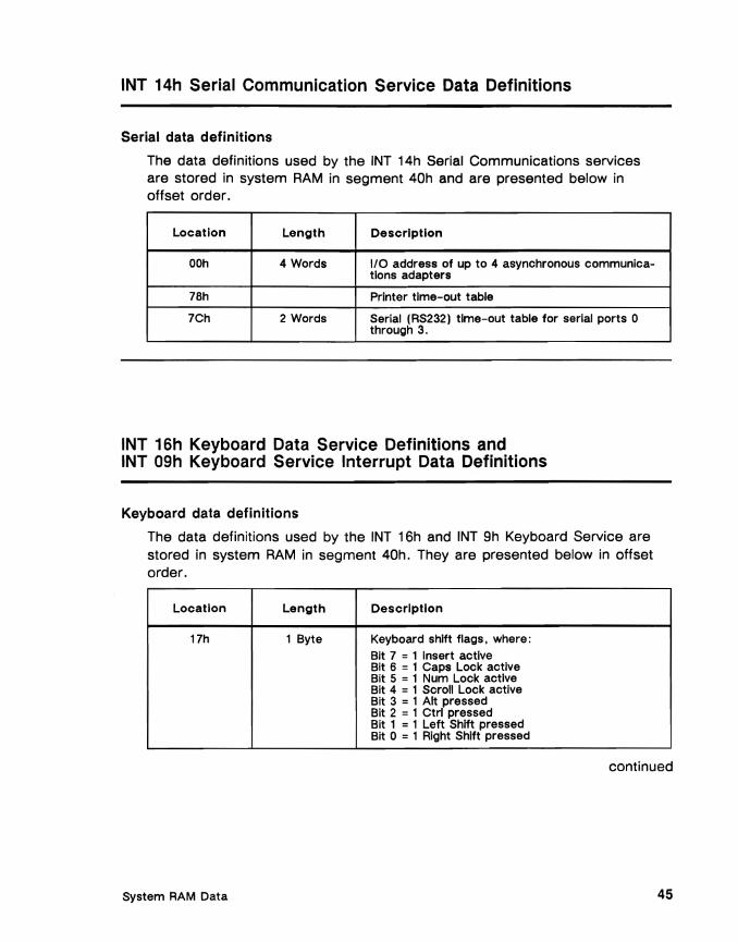
INT 14h Serial Communication Service Data Definitions
Serial data definitions
The data definitions used by the INT 14h Serial Communications services are stored in system RAM in segment 40h and are presented below in offset order.
Location Length Description
DOh 4 Words 1/0 address of up to 4 asynchronous communications adapters
78h Printer time-out table
7Ch 2 Words Serial (RS232) time-out table for serial ports 0 through 3.
INT 16h Keyboard Data Service Definitions and INT 09h Keyboard Service Interrupt Data Definitions
Keyboard data definitions
The data definitions used by the INT 16h and INT 9h Keyboard Service are stored in system RAM in segment 40h. They are presented below in offset order.
Location Length Description
17h 1 Byte Keyboard shift flags. where: Bit 7 = 1 Insert active Bit 6 = 1 Caps Lock active Bit 5 = 1 Num Lock active Bit 4 = 1 Scroll Lock active Bit 3 = 1 Alt pressed Bit 2 = 1 Ctrl pressed Bit 1 = 1 Left Shift pressed Bit 0 = 1 Right Shift pressed
continued
System RAM Data 45

INT 16h Keyboard Data Service Definitions and INT 09h Keyboard Service Interrupt Data Definitions, Continued
Keyboard data definitions, cant'd
Location Length Description
1Bh 1 Byte Extended keyboard shift flags, where: Bit 7 = 1 Insert pressed Bit 6 = 1 Caps Lock pressed Bit 5 = 1 Num Lock pressed Bit 4 = 1 Scroll Lock pressed Bit 3 =1 Ctrl-Num Lock state active Bit 2 =1 Sys Req pressed Bit 1 =1 Left Alt pressed Bit 0 =1 Left Ctrl pressed
19h 1 Byte Work area for Alt key and numeric keypad input
1Ah 1 Word Offset to next character in keyboard buffer
1Ch 1 Word Offset to first available spot In keyboard buffer
1Eh 16 Words Keyboard buffer of 16 word entries (a maximum of 15 are used at a time)
71h 1 Byte Bit 7 = 1 If Ctrl-Break pressed
72h 1 Word Reset flag. where: 1234h = Bypass memory test 4321 h =Preserve memory
BOh 1 Word Address to start of keyboard buffer (from segment 40h)
B2h 1 Word Address to end of keyboard buffer (from segment 40h)
96h 1 Byte Status byte:
Bit 7 =1 Read 10 in progress Bit 6 =1 Last code was first 10 Bit 5 =1 Forced Num Lock Bit 4 = 1 1011102 keyboard used Bit 3 =1 Right Alt active Bit 2 =1 Right Ctrl active Bit 1 =1 Last code was EOh Bit 0 =1 Last code was E1h
97h 1 Byte Status byte: Bit 7 =Error flag for keyboard command Bit 6 =LED update in progress Bit 5 =RESENO received from keyboard Bit 4 =ACK received from keyboard Bit 3 =Reserved Bit 2 =Current status of Caps Lock LED Bit 1 =Current status of Num Lock LED Bit 0 =Current status of Scroll Lock LED
System BIOS for IBM PC/XTI AT Computers and Compatibles 46

INT 17h Parallel ·Printer Service Data Definitions
The data definitions used by INT 17h Parallel Printer Service are stored in system RAM in segment 40h and are presented below in offset order.
Location Length Description
08h 4 Words 1/0 address of up to 4 printer adapters
78h 2 Words Printer time-out table for printers 1-3
10h 1 Word Number of devices installed. where: Bits 15-14 =Number of printer adapters Bits 13-12 =Reserved Bits 11-9 =Number of asynchronous adapters
(RS232) Bits 8 =Reserved Bits 7-6 =Number of disk drives. where:
OOb =1 Disk drive 01 b =2 Disk drives
Bits 5-4 =Initiai video mode, where: OOb =EGA or PGA 01 b =40x25 color 10b =80x25 color 11 b =80x25 black and white
Bit 3 =Reserved Bit 2 =Pointing device Bit 1 =1 If math coprocessor Bit 0 =Diskette available for boot
System RAM Data 47

INT 19h Bootstrap Loader Service Data Definitions
System RAM data
The data definitions used by INT 19h are stored in system RAM in segment 40h and are presented below in offset order.
Location Size Description
12h 1 Byte Reserved for manufacturers test, where: Bits 7-1 =Reserved Bit 0 =1 Manufacturing test mode
=0 Non-manufacturing test mode
72h 1 Word Reset flag, where: 1234h =Bypass memory test 4321h =Preserve memory 64h =Burn In mode
INT 1Ah Time-of-Day Service Data Definitions
Timer data definitions
The data definitions used by the INT 1Ah Time-of-Day Service and by the INT 08h Timer Interrupt are stored in system RAM in segment 40h and are presented below in offset order.
Location Length Description
6Ch 4 Bytes Timer tick count (count of timer ticks since midnight)
70h 1 Byte 24 hour rollover flag
98h 1 Word User walt flag offset address
9Ah 1 Word User wait flag segment address
9Ch 1 Word Least significant wait count
9Eh 1 Word Most significant wait count
AOh 1 Byte Wait active flag, where: Bit 7 = 1 If wait time elapsed Bits 6-1 = Reserved Bit 0 = 1 If INT 15h, AH = 86h wait has
occurred
System BIOS for IBM PC/XT I AT Computers and Compatibles 48
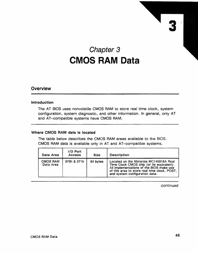
Chapter 3
CMOS RAM Data
Overview
Introduction
The AT BIOS uses nonvolatile CMOS RAM to store real time clock, system configuration, system diagnostic, and other information. In general, only AT and AT-compatible systems have CMOS RAM.
Where CMOS RAM data is located
The table below describes the CMOS RAM areas available to the BIOS. CMOS RAM data is available only in AT and AT-compatible systems.
1/0 Port Data Area Access Size Description
CMOS RAM Data Area
070h & 071h 64 bytes Located on the Motorola MC146818A Real Time Clock CMOS chip (or its equivalent). All implementations of the BIOS make use of this area to store real time clock, POST, and system configuration data.
continued
CMOS RAM Data 49
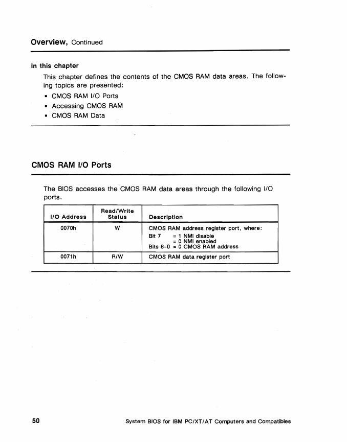
Overview, Continued
In this chapter
This chapter defines the contents of the CMOS RAM data areas. The following topics are presented:
• CMOS RAM 1/0 Ports
• Accessing CMOS RAM
• CMOS RAM Data
CMOS RAM I/O Ports
The BIOS accesses the CMOS RAM data areas through the following 1/0 ports.
Read/Write 1/0 Address Status Description
0070h W CMOS RAM address register port. where:
Bit 7 = 1 NMI disable = 0 NMI enabled
Bits 6-0 = 0 CMOS RAM address
0071h R/W CMOS RAM data register port
System BIOS for IBM PC/XT I AT Computers and Compatibles 50
Accessing CMOS RAM
MC146818A Real Time Clock
The AT BIOS supports a Motorola MC146818A or equivalent Real Time Clock. This chip is assumed to have at least 64 bytes of nonvolatile CMOS RAM available to store configuration data. The first nine bytes,· at offset locations OOh - 09h) are used to store RTC information. The next four bytes (offsets OAh - ODh) store status information. The balance of CMOS RAM storage (OEh - 3Fh) is used to store system configuration and other data.
Writing to CMOS RAM
The bit definitions for most of the standard CMOS RAM data definitions are provided in this chapter. To write data to CMOS RAM:
1. Inhibit interrupts.
2. Write the CMOS RAM address to which the data is to be written to 1/0 port 0070h.
3. Write the data to be written to 1/0 port 0071h.
Values can be written to CMOS RAM locations OOh - 09h much more quickly using INT 1Ah functions 02h - 07h.
Reading from CMOS RAM
The bit definitions for most of the standard CMOS RAM data definitions are provided in this chapter. To read from RTC CMOS RAM:
1. Inhibit interrupts.
2. Write the CMOS RAM address from which the data is to be read to I/O Port 0070h.
3. Read from 110 port 0071 h.
Values can be read from CMOS RAM locations OOh - 09h much more quickly using INT 1 Ah functions 02h - 07h.
CMOS RAM Data 51
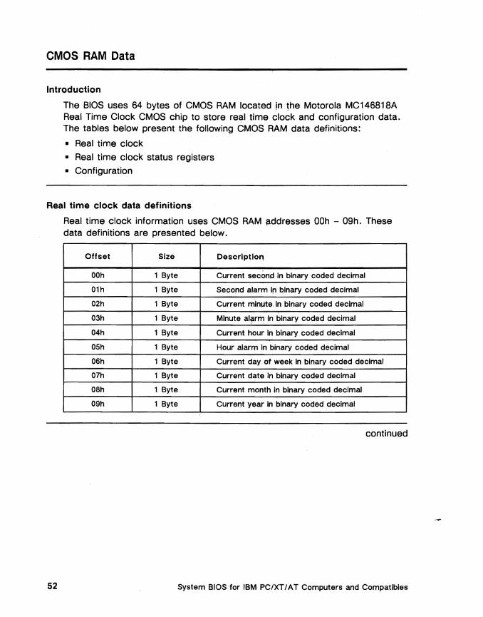
CMOS RAM Data
Introduction
The BIOS uses 64 bytes of CMOS RAM located jn the Motorola MC 14681 8A Real Time Clock CMOS chip to store real time Clock and configuration data. The tables below present the following CMOS RAM data definitions:
• Real time clock
• Real time clock status registers
• Configuration
Real time clock data definitions
Real time clock information uses CMOS RAM addresses OOh - 09h. These data definitions are presented below.
Offset Size Description
OOh 1 Byte Current second in binary coded decimal
01h 1 Byte Second alarm in binary coded decimal
02h 1 Byte Current mlnlJte In binary coded decimal
03h 1 Byte Minute aljlrm in binary coded decimal
04h 1 Byte Current hour in binary coded decimal
OSh 1 Byte Hour alarm In binary coded decimal
06h 1 Byte Current day of week in binary coded decimal
07h 1 Byte Current date In binary coded decimal
08h 1 Byte Current month in binary coded decimal
09h 1 Byte Current year In binary coded decimal
continued
System BIOS for IBM PC/XT / A T Computers and Compatibles 52

CMOS RAM Data, Continued
Status Registers data definitions
The real time status registers use CMOS RAM addresses OAh - ODh. These data definitions are presented below in offset order.
Location Size
OAh 1 Byte
OBh 1 Byte
OCh 1 Byte
ODh 1 Byte
Description
Status Register A. where: Bit 7 =1 Update In progress Bits 6-4 =Divider Identifying the time-based
frequency to use Bits 3-0 =Rate selection bits that define output
frequency and periodic Interrupt rate
Status Register B. where: Bit 7 =0 Run (update cycle)
=1 Abort any update cycle in progress Bit 6 =1 Enable periodic Interrupt Bit 5 =1 Enable alarm Interrupt Bit 4 =1 Enable update-ended interrupt Bit 3 =1 Enable square wave frequency set In
Status Register A Bit 2 =1 Calendar is in binary format
=0 Calendar is in BCD format Bit 1 =1 24-hour clock
=0 12-hour clock Bit 0 =1 Enable Daylight Savings Time
Status Register C. where: Bits 7-4 =IRQF. PF, AF. and UF flags, respec
tively. Only valid If alarm interrupt, update-ended interrupt or periodic interrupt Is enabled.
Bits 3-0 =Reserved
Status Register D, where: Bit 7 =1 Real time clock has power Bits 6-0 =Reserved
continued
CMOS 'RAM Data 53

CMOS RAM Data, Continued
Configuration data definitions
The system configuration information data definitions use CMOS RAM addresses OEh - 3Fh. These data definitions are presented below in offset order.
Location Size Description
OEh 1 Byte Diagnostic status. where:
Bit 7 = 1 Real time ciock lost power Bit 6 = 1 CMOS checksum is bad Bit 5 = 1 Invalid configuration information found
at POST Bit 4 = 1 Memory size compare error at POST Bit 3 = 1 Fixed disk or adapter fails initialization Bit 2 = 1 CMOS time found inva.lld Bit 1 = 1 Reserved Bit 0 = 1 Reserved
OFh 1 Byte Reason for shutdown. where: OOh = Power on or soft reset 01h = Memory size pass 02h = Memory test pass 03h = Memory test fail 04h = POST end; boot system OSh = JMP doubleword pointer with EOI 06h = Protected tests pass 07h = Protected tests fail 08h = Memory size fail 09h = INT 15h Block Move OAh = JMP double word pointer without EOI OBh = Used by 80386
10h 1 Byte Type of diskette drives: Bits 7-4 = Drive type of drive O. where:
OOOOb = No drive 0001 b = 360K drive 0010b = 1.2 MB drive 0011b = 720K 0100b = 1.44 MB
Bits 3-0 = Drive type of drive 1. where: OOOOb = No drive 0001b = 360K drive 0010b = 1.2 MB drive 0011b = 720K 0100b = 1.44 MB
11h 1 Byte Type of fixed disk drive 0 ~-., -
12h 1 Byte Type of fixed disk drive 1 . ~
13h 1 Byte Reserved
continued
System BIOS for IBM PC/XT I A T Computers and Compatibles 54

CMOS RAM Data, Continued
Configuration data definitions, cont'd
Location
l4h
15h
l6h
17h
1Sh
19h
1Ah
1Bh - 2Dh
2Eh -
2Fh
30h
31h
32h
33h
34h - 3Fh
Size
1 Byte
1 Byte
1 Byte
1 Byte
1 Byte
1 Byte
1 Byte
1 Byte
1 Byte
1 Byte
1 Byte
1 Byte
1 Byte
6 Words
Description
Equipment Installed. where: Bits 7-6 =Number of diskette drives. where:
OOb =1 Diskette drive 01b =2 Diskette drives
Bits 5-4 =Primary display. where:
OOb =Reserved 01b =CGA in 40-column mode lOb =CGA in SO-column mode llb =eGA in monochrome mode
Bits 3-2 =Reserved Bit 1 =1 Math coprocessor installed Bit 0 =0 Diskette drive installed
Base memory in 1 K. low byte
Base memory in 1K. high byte
Expansion memory in 1 K. low byte
Expansion memory in 1 K. high byte
Drive type of first fixed disk
Drive type of second fixed disk
Reserved
High byte checksum for 10h - 2Dh
Low byte checksum for 10h - 2Dh
Low byte of actual expansion memory size
High byte of actual expansion memory size
Century In BCD
Information flag
Reserved
CMOS RAM Data 55


Chapter 4
ROM BIOS Data
Overview
Introduction
In addition to the code for the various BIOS services, the BIOS also contains tapular data that is used to initialize devices. This data, particularly for fixed disk and diskette parameter tables, may be different for PC, XT, and AT systems. The differences are described in this chapter.
In this chapter
This chapter defines the contents of the ROM BIOS data areas. The following topics arE;! presented:
• ROM A~dress Compatibility Table
• SystE;lm Configuration Data Table
• Diskette Parameter Table
• AT Fixed Disk Parameter Table
• XT Fixed Disk Parameter Table
• Bau9 Rate Initialization
ROM BIOS Data 57

ROM Address Compatibility Table
Description
The BIOS maintains compatibility between PC, XT, and AT versions by providing a list of jump instructions that insure that both table information and calls to specific BIOS services are located at fixed entry points.
ROM BIOS address map
Address Description
FE05Bh POST Entry Point
FE2C3h NMI Handler Entry Point
FE3FEh INT 13h Fixed Disk Service Entry Point
FE401h Fixed Disk Parameter Table
FE6F2h INT 19h Boot Load Service Entry Point
FE6F5h Configuration Data Table
FE729h Baud Rate Generator Table
FE739h INT 14h Serial Communications Service Entry Point
FE82Eh INT 16h Keyboard Service Entry Point
FE987h INT 09h Keyboard Service Entry Point
FEC59h INT 13h Diskette Service Entry Point
FEF57h INT OEh Diskette Hardware ISR Entry Point
FEFC7h Diskette Controller Parameter Table
FEFD2h INT 17h Printer Service Entry Point
FF045h INT 10 Functions O-Fh Entry Point
FF065h INT 10h Video Support Service Entry Point
FFOA4h MDA/CGA Video Parameter Table (INT 1 Dh)
FF841h INT 12h Memory Size Service Entry Point
FF84Dh INT 11 h Equipment List Service Entry Point
FF859h INT 15h System Services Entry Point
FFA6Eh Character Font for 320X200 and 640X200 Graphics (lower 128
FFE6Eh
FFEA5h
characters)
INT 1 Ah Time-of-day Service Entry Point
INT 08h System Timer ISR Entry Point
continued
System BIOS for IBM PC/XT I AT Computers and Compatibles 58
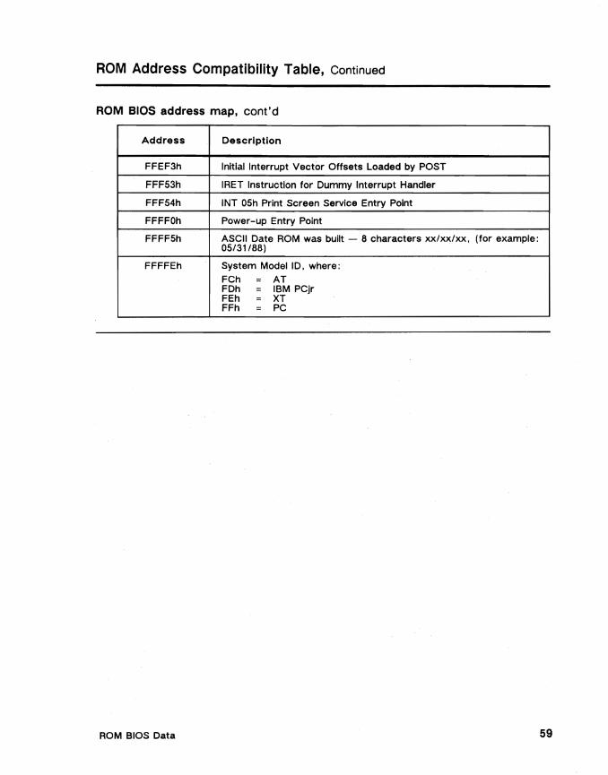
ROM Address Compatibility Table, Continued
ROM BIOS address map, cont'd
Address Description
FFEF3h Initial Interrupt Vector Offsets Loaded by POST
FFF53h IRET Instruction for Dummy Interrupt Handler
FFF54h INT 05h Print Screen Service Entry Point
FFFFOh Power-up Entry Point
FFFF5h ASCII Date ROM was built - 8 characters xx/xx/xx. (for example: 05/31/88)
FFFFEh System Model ID. where: FCh = AT FDh = IBM PCjr FEh = XT FFh = PC
ROM BIOS Data 59

System Configuration Data Table (AT only)
Description
The System Configuration Table is located at FOOO:E6F5h. This table can be called into RAM via INT 15h Function AH = COh Return System Configuration Parameters.
Offset Initial (hex) Value Length Description
OOh OOh 2 Bytes Number of bytes in this table (minimum =8)
02h 02h 1 Byte Model byte, where:
PC =FFh PC XT =FEh PC XT =FBh PCjr =FDh AT =FCh XT-286 =FCh PC Convertible =F9h Unknown system board =FFh
03h 03h 1 Byte Submodel byte, where: PC =OOh PC XT =OOh PCjr =OOh AT =OOh AT =01h XT-286 =02h PC Convertible =OOh Unknown system board =FFh
04h 04h 1 Byte BIOS revision level (first release =OOb)
OSh OSh 1 Byte Feature Information byte, where: Bit 7 =1 Fixed disk BIOS uses DMA channel 3 Bit 6 =1 Second Interrupt chip present Bit S =1 Real time clock present Bit 4 =1 Keyboard intercept (INT 15h, Function
AH =4Fh) called by keyboard Interrupt service (INT 09h)
Bit 3 =1 Wait for external event supported Bit 2 = Reserved Bit 1 =0 PC-type I/O channel implemented Bit 0 =0 Reserved
06h 06h 1 Byte Feature Information byte 2 (reserved. zeros)
07h 07h 1 Byte Feature Information byte 3 (reserved, zeros)
08h 08h 1 Byte Feature information byte 4 (reserved, zeros)
09h 09h 1 Byte Feature information byte 5 (reserved, zeros)
System BIOS for IBM PC/XT/AT Computers and Compatibles 60
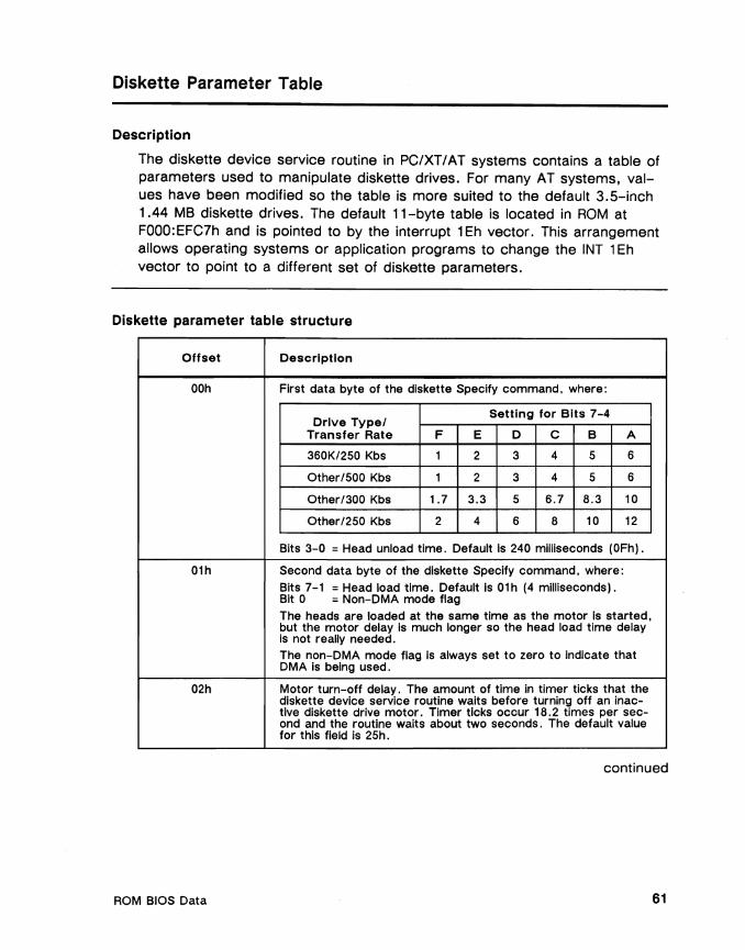
Diskette Parameter Table
Description
The diskette device service routine in PC/XT / AT systems contains a table of parameters used to manipulate diskette drives. For many AT systems, values have been modified so the table is more suited to the default 3.5-inch 1.44 MB diskette drives. The default 11-byte table is located in ROM at FOOO:EFC7h and is pointed to by the interrupt 1 Eh vector. This arrangement allows operating systems or application programs to change the INT 1Eh vector to point to a different set of diskette parameters.
Diskette parameter table structure
Offset Description
OOh First data byte of the diskette Specify command, where:
Setting for Bits 7-4 Drive Type/
Transfer Rate F E D C B A
360K/250 Kbs 1 2 3 4 5 6
Other/500 Kbs 1 2 3 4 5 6
Other/300 Kbs 1.7 3.3 5 6.7 8.3 10
Other/250 Kbs 2 4 6 8 10 12
Bits 3-0 =Head unload time. Default Is 240 milliseconds (OFh).
01h Second data byte of the diskette Specify command, where:
Bits 7-1 =Head load time. Default Is 01h (4 milliseconds). Bit 0 =Non-DMA mode flag The heads are loaded at the same time as the motor is started, but the motor delay Is much longer so the head load time delay is not really needed. The non-DMA mode flag is always set to zero to indicate that DMA is being used.
02h Motor turn-off delay. The amount of time in timer ticks that the diskette device service routine walts before turning off an inactive diskette drive motor. Timer ticks occur 18.2 times per second and the routine walts about two seconds. The default value for this field is 25h.
continued
ROM BIOS Data 61

Diskette Parameter Table, Continued
Diskette parameter table structure, cont'd
Offset Description
03h Bytes per sector. This field Is encoded In the following way to match the encoding used by the diskette controller:
OOh = 128 bytes per sector 01h = 256 bytes per sector 02h = 512 bytes per sector (default value) 03h = 1024 bytes per sector
04h The number of sectors per track. For a 1.44 MB diskette In the 1.44 MB drive. this field Is 18 sectors per track. The range of values Is:
08h = 8 sectors per track (320K drive) 09h = 9 sectors per track (360K/720K 5.25-lnch drive) 15h = 15 sectors per track (5.25-lnch 1.2 MB drive) 18h = 18 sectors per track (3. 5-inch drives)
05h Gap length. The length of the gap between sectors. 1 Bh for a 3.5-inch diskette drive and 2Ah for a 5.25-inch diskette drive.
06h Data length. Since the bytes per sector field is nonzero, this field is meaningless and Is set to FFh.
07h Gap length for format. The length of the gap between sectors to maintain when formatting. The format gap length is 6Ch for a 3.5-inch drive and 50h for a 5.25-inch drive.
08h Fill byte for format. The default Is F6h.
09h Head settle time. The amount of time in milliseconds the diskette DSR must wait for the heads to settle after doing a seek operation. For a 3. 5-inch diskette drive, this field is OFh. 1.2MB drives require 15 milliseconds and 360K drives. 20 - 25 milliseconds.
OAh Motor start time. The amount of time in eighths of a second that the diskette DSR must walt for the motor to come up to speed before doing an I/O operation. Most drives have a motor start time of one second so the default value is 08h for most operations. except Read and Verify. where the default value Is either 04h or 05h.
System BIOS for IBM PC/XT I AT Computers and Compatibles 62
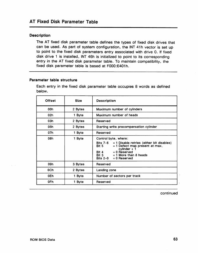
AT Fixed Disk Parameter Table
Description
The AT fixed disk parameter table defines the types of fixed disk drives that can be used. As part of system configuration, the INT 41 h vector is set up to point to the fixed disk parameters entry associated with drive O. If fixed disk drive 1 is installed, INT 46h is initialized to point to its corresponding entry in the AT fixed disk parameter table. To maintain compatibility, the fixed disk parameter table is based at FOOO:E401 h.
Parameter table structure
Each entry in the fixed disk parameter table occupies 8 words as defined below.
Offset Size Description
OOh 2 Bytes Maximum number of cylinders
02h 1 Byte Maximum number of heads
03h 2 Bytes Reserved
05h 2 Bytes Starting write precompensation cylinder
07h 1 Byte Reserved
08h 1 Byte Control byte, where: Bits 7-6 = 1 Disable retries (either bit disables) Bit 5 = 1 Defect map present at max,
cylinder + 1 Bit 4 = 0 Reserved Bit 3 = 1 More than 8 heads Bits 2-0 = 0 Reserved
09h 3 Bytes Reserved
OCh 2 Bytes Landing zone
OEh 1 Byte Number of sectors per track
OFh 1 Byte Reserved
continued
ROM BIOS Data 63
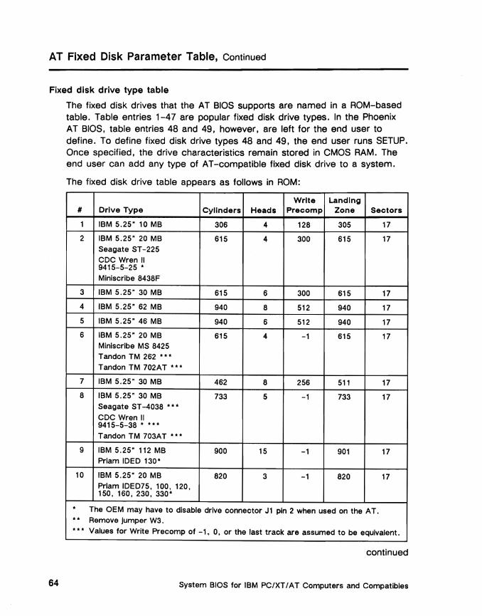
AT Fixed Disk Parameter Table, Continued
Fixed disk drive type table
The fixed disk drives that the AT BIOS supports are named in a ROM-based table. Table entries 1-47 are popular fixed disk drive types. In the Phoenix AT BIOS, table entries 48 and 49, however, are left for the end user to define. To define fixed disk drive types 48 and 49, the end user runs SETUP. Once specified, the drive characteristics remain stored in CMOS RAM. The end user can add any type of AT-compatible fixed disk drive to a system.
The fixed disk drive table appears as follows in ROM:
# Drive Type Cylinders Heads Write
Precomp Landing
Zone Sectors
1 iBM 5.25" 10 MB 306 4 128 305 17
2 IBM 5.25" 20 MB Seagate ST -225 CDC Wren II 9415-5-25 • Minlscribe 8438F
615 4 300 615 17
3 IBM 5.25" 30 MB 615 6 300 615 17
4 IBM 5.25" 62 MB 940 8 512 940 17
5 IBM 5.25" 46 MB 940 6 512 940 17
6 IBM 5.25" 20 MB Mlnlscrlbe MS 8425 Tandon TM 262 ••• Tandon TM 702AT •••
615 4 -1 615 17
7 IBM 5.25" 30 MB 462 8 256 511 17
8 IBM 5.25" 30 MB Seagate ST -4038 •••
CDC Wren II 9415-5-38 ••••
Tandon TM 703AT •••
733 5 -1 733 17
9 IBM 5.25" 112 MB Priam IDEO 130·
900 15 -1 901 17
10 IBM 5.25" 20 MB Priam IDED75, 100, 120,
820 3 -1 820 17
150, 160, 230, 330·
• The OEM may have to disable drive connector J1 pin 2 when used on the AT . •• Remove jumper W3 . ••• Values for Write Precomp of -1. 0, or the last track are assumed to be equivalent.
continued
System BIOS for IBM PC/XT/AT Computers and Compatibles 64
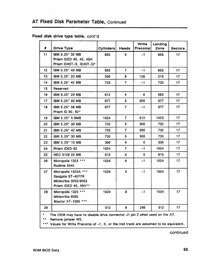
AT Fixed Disk Parameter Table, Continued
Fixed disk drive type table, cont'd
Write Landing # Drive Type Cylinders Heads Precomp Zone Sectors
11 IBM 5.25" 35 MB 855 5 -1 855 17 Priam IDEO 40, 45. 45H Priam ID45T -S, ID45T-Q"
12 IBM 5.25" 49 MB 855 7 -1 855 17
13 IBM 5.25" 20 MB 306 8 128 319 17
14 IBM 5.25" 42 MB 733 7 -1 733 17
15 Reserved
16 IBM 5.25" 20 MI3 612 4 0 663 17
17 IBM 5.25" 40 MB 977 5 300 977 17
18 IBM 5.25" 56 MB 977 7 -1 977 17 Priam 10 60, 62"
19 IBM 5.25" 59MB 1024 7 512 1023 17
20 IBM 5.25" 30 MB 733 5 300 732 17
21 IBM 5.25" 42 MB 733 7 300 732 17
22 IBM 5.25" 30 MB 733 5 300 733 17
23 IBM 5.25" 10 MB 306 4 0 336 17
24 Priam IDEO 62 1024 7 -1 1024 17
25 NEC 5126 20 MB 615 4 0 615 17
26 Micropolls 1323 """ 1024 4 -1 1024 17
BO.dime 5040
27 Micropolls 1323A """ 1024 5 -1 1024 17 Si;!agate ST -4077R Miniscrlbe 3053/6053 Priam IDEO 45, 45H""
28 Micropolls 1325 """ 1024 8 -1 1024 17 Miniscribe 6085
Maxtor XT-1085 """
29 512 8 256 512 17
The OEM may have to disable drive connector J1 pin 2 when used on the AT." Remove jumper W3.
""" Values for Write Precomp of -1, 0, or the I~.st track are assumed to be equivalent.
continued
""
ROM BIOS Data 65

AT Fixed Disk Parameter Table, Continued
Fixed disk drive type table, cont'd
Write Landing
# Drive Type Cylinders Heads Precomp Zone Sectors
30 Syquest SQ312RD •• 615 2 615 615 17
Minlscribe MS 8212 •••
31 CDC Wren II 9420-5-51 •• 989 5 0 989 17
32 1020 15 -1 1024 17
33 Reserved
34 Reserved
35 Seagate ST -4096 1024 9 1024 1024 17
Seagate ST -4144 Seagate ST -4144R 26
36 Minlscrlbe MS 6053 1024 5 512 1024 17
Microscience HHl050
37 830 10 -1 830 17
38 NEC 67 MB 823 10 256 824 17
39 NEC D5126H 20 MB 615 4 128 664 17
40 IBM 5.25" 40 MB 615 8 128 664 17 NEC D5146H
41 IBM 5.25" 114 MB 917 15 -1 918 17
42 IBM 5.25" 127 MB 1023 15 -1 1024 17 Priam IDEO 130"
43 NEC 823 10 512 823 17
44 Seagate ST -251 40 MB 820 6 -1 820 17
45 Reserved
46 CDC Wren II (1) 9415-5-86
925 9 -1 925 17
47 699 7 256 700 17
48 Configurable by end user
49 Configurable by end user
• The OEM may have to disable drive connector J1 pin 2 when used on the AT . •• Remove jumper W3 . ••• Values for Write Precomp of -1, 0, or the last track are assumed to be equivalent .
continued
System BIOS for IBM PC/XT I AT Computers and Compatibles 66
AT Fixed Disk Parameter Table, Continued
Fixed disk drive type table, cont'd
If a table entry contains -1 for Write Precompensation, then there is no write precompensation for this fixed disk drive type. If the Write Precompensation is zero, then there is write precompensation for all cylinders.
Drive types 48 and 49 in a Phoenix BIOS can be eoited by the Phoenix SETUP utility. Parameter values entered in SETUP for these drives are stored in CMOS RAM.
ROM BIOS Data 67

XT Fixed Disk Parameter Table
Description
The XT fixed disk parameter table defines the types of fixed disk drives that can be used in an XT system. As part of system configuration, the INT 41 h vector is set up to point to the fixed disk parameter entry associated with drive O. To maintain compatibility, the fixed disk parameter table is based at FOOO:E401 h.
Parameter table structure
Each entry in the fixed disk parameter table occupies 16 bytes as defined below.
Offset Bytes Description
OOh 2 Maximum number of cylinders
02h 1 Maximum number of heads
03h 2 Starting reduced write current cylinder
05h 2 Starting write precompensation cylinder
07h 1 Maximum ECC burst length
08h 1 Control byte. where: Bit 7 = 1 Disable fixed disk retries Bit 6 = 1 Disable ECC retries Bits 5-3= 1 Reserved Bits 2-0= Drive option
09h 1 Standard timeout value
OAh 1 Time-out value for format drive command
OBh 1 Time-out value for check drive command
OCh 4 Reserved
continued
System BIOS for IBM PC/XTIA T Computers and Compatibles 68

XT Fixed Disk Parameter Table, Continued
XT fixed disk drive type table
There are four fixed disk drive types supported by the XT -compatible Fixed Disk Service. The parameters for each of these XT-compatible drive types are:
Parameter Type 0 Type 1 Type 2 Type 3
Maximum cylinders 306 612 615 306
Maximum head(s) 4 4 4 8
Reduced write current cyl. 306 612 615 306
Write precomp cylinder 0 0 300 128
ECC Data Burst Length 11 11 11 11
Control byte 5 5 5 5
Standard time-out 12 32 24 12
Format drive time-out 180 180 180 180
Check drive time-out 40 40 40 40
Reserved 0 0 0 0
Reserved 0 0 0 0
Reserved 0 0 0 0
Reserved 0 0 0 0
ROM BIOS Data 69
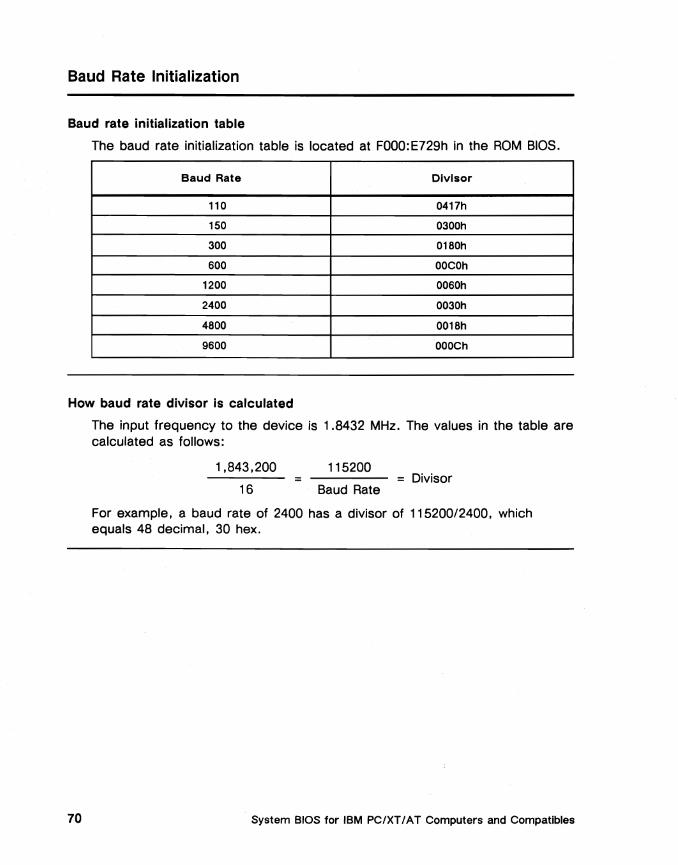
Baud Rate Initialization
Baud rate initialization table
The baud rate initialization table is located at FOOO:E729h in the ROM BIOS.
Baud Rate Divisor
110 0417h
150 0300h
300 0180h
600 OOCOh
1200 0060h
2400 0030h
4800 0018h
9600 OOOCh
How baud rate divisor is calculated
The input frequency to the device is 1.8432 MHz. The values in the table are calculated as follows:
1,843,200 115200 = = Divisor
16 Baud Rate
For example, a baud rate of 2400 has a divisor of 115200/2400, which equals 48 decimal, 30 hex.
System BIOS for IBM PC/XT I A T Computers and Compatibles 70
Chapter 5
1/0 Port Addresses
Overview
1/0 Ports
In the PC, XT, and AT architecture, the bus can address either system memory or 1/0. Four bytes are used for the address formation, so I/O port addresses can range from OOOOh to FFFFh for a total of 64K locations. The microprocessor can address as many I/O locations as it can address memory locations in any given memory segment. In an AT system, addresses OOOOh to OOFFh are reserved for the system board and addresses 0100h 03FFh are reserved for the I/O channel.
This I/O addressing capability gives the ISA architecture considerable power in that a system is able to access I/O devices through a broad range of addresses.
Standard I/O port protocols have been established for many common input devices. These standard I/O port address definitions are presented in the following pages. Where possible, we have provided exact bit definitions for I/O ports. Note that some IBM-compatible systems use nonstandard I/O devices or nonstandard I/O port definitions. For instance, the location of the third and fourth serial ports, given here as 3220h and 3228h, may vary from system to system.
110 Port Addresses 71

Hardware 1/0 Port List
1/0 Address
OOOOh
0001h
0002h
0003h
0004h
0005h
0006h
0007h
OOOBh
OOOAh
OOOBh
Read/Wrlte Status
R/W
R/W
R/W
R/W
R/W
R/W
R/W
R/W
R
R/W
W
Description
DMA channel 0, memory address register
DMA channel 0, transfer count register
DMA channel 1, memory address register
DMA channel 1, transfer count register
DMA channel 2, memory address register
DMA channel 2, transfer count register
DMA channel 3, memory address register
DMA channel 3, transfer count register
DMA channel 0-3, status register, where:
Bit 7 =1 Channel 3 request Bit 6 =1 Channel 2 request Bit 5 =1 Channel 1 request Bit 4 =1 Channel 0 request Bit 3 =1 Terminal count on channel 3 Bit 2 =1 Terminal count on channel 2 Bit 1 =1 Terminal count on channel 1 Bit 0 =1 Terminal count on channel 0
DMA channel 0-3, mask register, where: Bits 7-3 =0 Reserved Bit 2 =0 Clear mask Bit
=1 Set mask Bit Bits 1-0 =OOb Select channel 0
=01b Select channel 1 =1Ob Select channel 2 =11b Select channel 3
DMA channel 0-3, mode register, where:
Bits 7-6 =OOb Demand mode =01b Signal mode =10b Block mode =11 b Cascade mode
Bits 5-4 =0 Reserved Bits 3-2 =OOb Verify operation
=01 b Write operation =10b Read operation =11b Reserved
Bits 1-0 =OOb Select channel 0 =01 b Select channel 1 =1Ob Select channel 2 =11 b Select channel 3
continued
System BIOS for IBM PC/XT I AT Computers and Compatibles 72
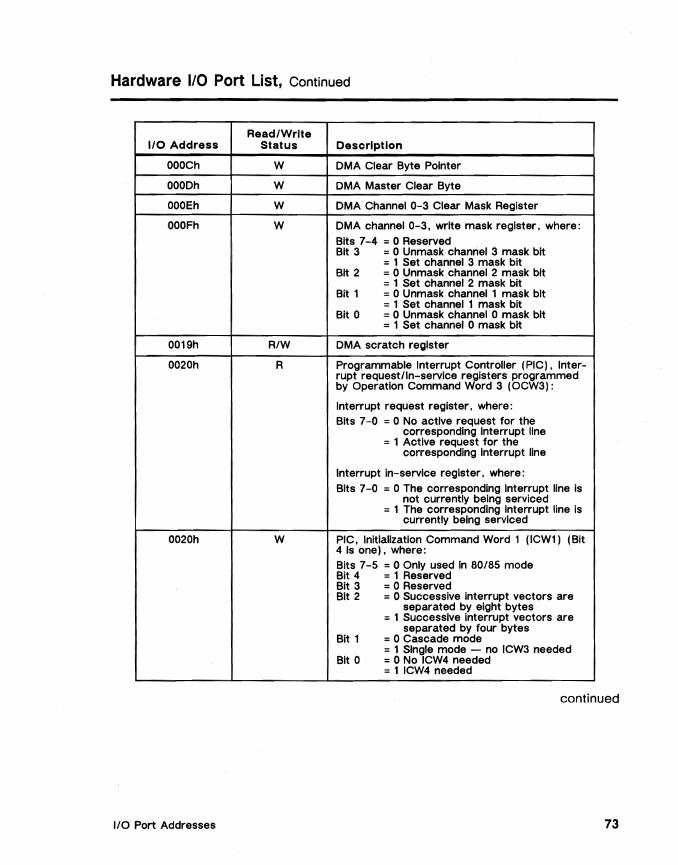
Hardware 1/0 Port List, Continued
I/O Address
OOOCh
OOODh
OOOEh
OOOFh
0019h
0020h
0020h
Read/Write Status
W
W
W
W
R/W
R
W
Description
DMA Clear Byte Pointer
DMA Master Clear Byte
DMA Channel 0-3 Clear Mask Register
DMA channel 0-3. write mask register. where: Bits 7-4 =0 Reserved Bit 3 =0 Unmask channel 3 mask bit
=1 Set channel 3 mask bit Bit 2 =0 Unmask channel 2 mask bit
=1 Set channel 2 mask bit Bit 1 =0 Unmask channel 1 mask bit
=1 Set channel 1 mask bit Bit 0 =0 Unmask channel 0 mask bit
=1 Set channel 0 mask bit
DMA scratch register
Programmable Interrupt Controller (PIC). Interrupt requestlln-service registers programmed by Operation Command Word 3 (OCW3):
Interrupt request register. where: Bits 7-0 =0 No active request for the
corresponding interrupt line =1 Active request for the
corresponding interrupt line
Interrupt In-service register. where: Bits 7-0 =0 The corresponding interrupt line is
not currently being serviced =1 The corresponding interrupt line is
currently being serviced
PIC. Initialization Command Word 1 (ICW1) (Bit 4 is one). where: Bits 7-5 Bit 4 Bit 3 Bit 2
Bit 1
Bit 0
=0 Only used in 80/85 mode =1 Reserved =0 Reserved =0 Successive interrupt vectors are
separated by eight bytes =1 Successive interrupt vectors are
separated by four bytes =0 Cascade mode =1 Single mode - no ICW3 needed =0 No ICW4 needed =1 ICW4 needed
continued
I/O Port Addresses 73
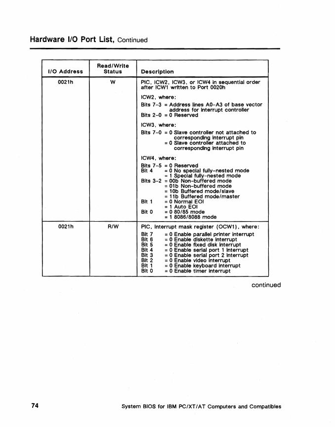
Hardware 1/0 Port List, Continued
Read/Write I/O Address Status
0021h W
0021h R/W
Description
PIC, ICW2, ICW3, or ICW4 In sequential order . after ICW1 written to Port 0020h
ICW2, where: Bits 7-3 =Address lines AO-A3 of base vector
address for Interrupt controller Bits 2-0 =0 Reserved
ICW3, where: Bits 7-0 =0 Slave controller not attached to
corresponding Interrupt pin =0 Slave controller attached to
corresponding Interrupt pin
ICW4, where: Bits 7-5 Bit 4
Bits 3-2
Bit 1
Bit 0
=0 Reserved =0 No special fully-nested mode =1 Special fully-nested mode =OOb Non-buffered mode =01b Non-buffered mode = lOb Buffered mode/slave =11 b Buffered mode/master =0 Normal EOI =1 Auto EOI =0 80/85 mode =1 8086/8088 mode
PIC, Interrupt mask register (OCW1), where: Bit 7 Bit 6 Bit 5 Bit 4 Bit 3 Bit 2 Bit 1 Bit 0
=0 Enable parallel printer interrupt =0 Enable diskette Interrupt =0 Enable fixed disk interrupt =0 Enable serial port 1 interrupt =0 Enable serial port 2 Interrupt =0 Enable video Interrupt = 0 Enable keyboard interrupt =0 Enable timer interrupt
continued
System BIOS for IBM PC/XT / A T Computers and Compatibles 74
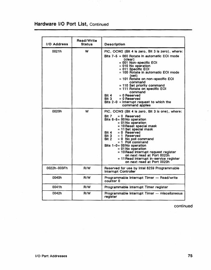
Hardware 110 Port List, Continued
ReadlWrite 1/0 Address Status Description
0021h W PIC, OCW2 (Bit 4 Is zero, Bit 3 Is zero), where: Bits 7-5 = 000 Rotate In automatic EOI mode
(clear) = 001 Non-specific EOI = 010 No operation = 011 Specific EOI = 100 Rotate In automatic EOI mode
(set) = 101 Rotate on non-specific EOI
command = 110 Set priority command = 111 Rotate on specific EOI
command Bit 4 = 0 Reserved Bit 3 = 0 Reserved Bits 2-0 = Interrupt request to which the
command applies
0020h W PIC, OCW3 (Bit 4 Is zero, Bit 3 Is one), where: Bit 7 = 0 Reserved Bits 6-5= 00 No operation
= 01 No operation = 10 Reset special mask = 11 Set special mask
Bit 4 = 0 Reserved Bit 3 = 1 Reserved Bit 2 = 0 No poll command
= 1 Poll command Bits 1-0= ~ONo operation
= 01 No operation =10 Read Interrupt request register
on next read at Port 0020h =11 Read Interrupt In-service register
on next read at Port 0020h
0022h-003Fh R/W Reserved for use by Intel 8259 Programmable Interrupt Controller
0040h R/W Programmable Interrupt Timer - Read/write counter 0
0041h R/W Programmable Interrupt Timer register
0042h R/W Programmable Interrupt Timer - miscellaneous register
continued
I/O Port Addresses 75

Hardware 1/0 Port List, Continued
I/O Address
0043h
0044h
0047h
0048h-005Fh
0060h
0060h
0061h
Read/Write Status
W
W
W
R/W
W
R
R/W
Description
Programmable Interrupt Timer. control word register for counters 0 and 2. where: Bits 7-6 =OOb Select counter 0
=01b Reserved = lOb Select counter 2
Bits 5-4 =OOb Counter latch command =01b Read/write counter bits 0-7
only = lOb Read/write counter bits 8-15
only = 11 b Read/write counter bits 0-7
first. then bits 8-15 Bits 3-0 = OOOb Mode 0 select
=001 b Mode 1 select =Xl0b Mode 2 select = Xllb Mode 3 select = 100b Mode 4 select = 101 b Mode 5 select
Bit 0 = 0 Binary counter 16 bits = 1. Binary coded decimal counter
Programmable Interrupt Timer. miscellaneous register (AT only)
Programmable Interrupt Timer. control word register for counter 0 (AT only). where: Bits 7-6 = OOb Select counter 0
= 01b Reserved = lOb Reserved = 11b Reserved
Bits 5-4 = OOb Counter latch command select counter 0
= 01b Read/write counter bits 0-7 only
= lOb Reserved = 11 b Reserved
Used by Programmable Interrupt Timer
Keyboard data Input buffer (AT only)
Keyboard data output buffer (AT only)
8042 control register (AT only), where: Bit 7 = 1 Parity check Bit 6 = 1 Channel check Bit 5 = 1 Timer 2 output Bit 4 = 1 Toggle with each refresh request Bit 3 =0 Channel check enabled Bit 2 = 0 Parity check enabled Bit 1 = 1 Speaker data enabled Bit 0 = 1 Timer 2 gate to speaker enabled
continued
System BIOS for IBM PC/XT / A T Computers and Compatibles 76

Hardware 1/0 Port List, Continued
Read/Write 110 Address Status Description
0061h W 8255 output register (XT only), where:
Bit 7 =1 Clear keyboard) Bit 6 =0 Hold keyboard clock low Bit 5 =0 Enable 110 check Bit 4 =0 Enable RAM parity check Bit 3 =0 Read low switches Bit 2 =Reserved Bit 1 =1 Speaker data enable Bit 0 =1 Enable timer 2 gate to speaker
0062h R/W 8255 input register (XT only), where:
Bit 7 =1 RAM parity check Bit 6 =1 110 channel check Bit 5 =1 Timer channel 2 out Bit 4 =Reserved Bit 3 =1 System board RAM size type 1 Bit 2 =1 System board RAM size type 0 Bit 1 =1 Coprocessor installed Bit 0 =1 Loop in POST
0063h R/W 8255 Command mode register (XT only), where: Bits 7-6
Bits 5-4
Bits 3-2
Bits 3-2
Bits 1-0
=Number of diskette drives, where: OOb - 1 drive 01 b - 2 drives 10b - 3 drives 11 b -4 drives
=Type of display at power-on, where: OOb - Reserved 01b - 40x25 color (mono mode) 10b - 80x25 color (mono mode) 11b - MDA (80x25)
=Memory on system board (256K chips), where: OOb - 256K 01b - 512K 10b - 576K 11b - 640K
=Memory on system board 964K chips), where: OOb - 64K 01b - 128K 10b - 192K 11b - 256K
=Reserved
continued
110 Port Addresses 17
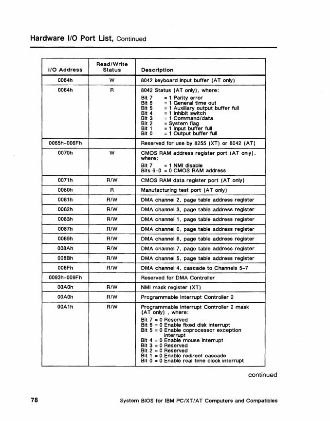
Hardware 110 Port List, Continued
I/O Address
0064h
0064h
0065h-006Fh
0070h
0071h
0080h
0081h
0082h
0083h
0087h
0089h
008Ah
008Bh
008Fh
0093h-009Fh
OOAOh
OOAOh
00A1h
Read/Write Status
W
R
W
R/W
R
R/W
R/W
R/W
R/W
R/W
R/W
R/W
R/W
R/W
R/W
R/W
Description
8042 keyboard Input buffer (AT only)
8042 Status (AT only), where:
Bit 7 =1 Parity error Bit 6 =1 General time out Bit 5 =1 Auxiliary output buffer full Bit 4 =1 Inhibit switch Bit 3 =1 Command/data Bit 2 =System flag Bit 1 =1 Input buffer full Bit 0 =1 Output buffer full
Reserved for use by 8255 (XT) or 8042 (AT)
CMOS RAM address register port (AT only) , where: Bit 7 =1 NMI disable Bits 6-0 =0 CMOS RAM address
CMOS RAM data register port (AT only)
Manufacturing test port (AT only)
DMA channel 2. page table address register
DMA channel 3. page table address register
DMA channel 1. page table address register
DMA channel O. page table address register
DMA channel 6, page table address register
DMA channel 7. page table address register
DMA channel 5, page table address register
DMA channel 4. cascade to Channels 5-7
Reserved for DMA Controller
NMI mask register (XT)
Programmable Interrupt Controller 2
Programmable Interrupt Controller 2 mask (AT only) , where: Bit 7 =0 Reserved Bit 6 =0 Enable fixed disk Interrupt Bit 5 =0 Enable coprocessor exception
interrupt Bit 4 =0 Enable mouse interrupt Bit 3 =0 Reserved Bit 2 =0 Reserved Bit 1 =0 Enable redirect cascade Bit 0 =0 Enable real time clock interrupt
continued
System BIOS for IBM PC/XT / A T Computers and Compatibles 78

Hardware I/O Port List, Continued
I/O Address
OOCOh
00C2h
00C4h
OOC6h
00C8h
OOCAh
OOCCh
OOCEh
OODOh
00D2h
00D4h
Read/Write Status
R/W
R/W
R/W
R/W
R/W
R/W
R/W
R/W
R
W
R/W
Description
DMA channel 0 (AT only). memory address register
DMA channel 0 (AT only). transfer count register
DMA channell .(AT only). memory address register
DMA channell (AT only). transfer count register
DMA channel 2 (AT only). memory address register
DMA channel 2 (AT only). transfer count register
DMA channel 3 (AT only). memory address register
DMA channel 3 (AT only). transfer address register
DMA status register (AT only). where: Bit 7 =1 Channel 7 request Bit 6 =1 Channel 6 request Bit 5 =1 Channel 5 request Bit 4 =1 Channel 4 request Bit 3 =1 Terminal count on channel 7 Bit 2 =1 Terminal count on channel 6 Bit 1 =1 Terminal count on channel 5 Bit 0 =1 Terminal count on channel 4
DMA Write request register (AT only)
DMA mask register (AT only). where: Bits 7-3 =0 Reserved Bit 2 =0 Clear mask bit
=1 Set mask bit Bits 1-0 =OOb Select channel 4
=01 b Select channel 5 = lOb Select channel 6 =11 b Select channel 7
continued
I/O Port Addresses 79
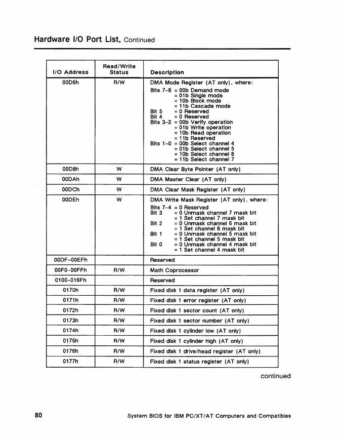
Hardware 1/0 Port List, Continued
I/O Address
00D6h
00D8h
OODAh
OODCh
OODEh
OODF-OOEFh
OOFO-OOFFh
0100-0l6Fh
0170h
017lh
0172h
0173h
0174h
0175h
0176h
0177h
Read/Write Status
R/W
W
W
W
W
R/W
R/W
R/W
R/W
R/W
R/W
R/W
R/W
R/W
Description
DMA Mode Register (AT only). where: Bits 7-6 =OOb Demand mode
=01b Single mode = lOb Block mode =11 b Cascade mode
Bit 5 =0 Reserved Bit 4 =0 Reserved Bits 3-2 =OOb Verify operation
=01b Write operation =lOb Read operation =11 b Reserved
Bits 1-0 =OOb Select channel 4 =01 b Select channel 5 =lOb Select channel 6 =11 b Select channel 7
DMA Clear Byte Pointer (AT only)
DMA Master Clear (AT only)
DMA Clear Mask Register (AT only)
DMA Write Mask Register (AT only). where: Bits 7-4 =0 Reserved Bit 3 =0 Unmask channel 7 mask bit
=1 Set channel 7 mask bit Bit 2 =0 Unmask channel 6 mask bit
=1 Set channel 6 mask bit Bit 1 =0 Unmask channel 5 mask bit
=1 Set channel.5 mask bit Bit 0 =0 Unmask channel 4 mask bit
=1 Set channel 4 mask bit
Reserved
Math Coprocessor
Reserved
Fixed disk 1 data register (AT only)
Fixed disk 1 error register (AT only)
Fixed disk 1 sector count (AT only)
Fixed disk 1 sector number (AT only)
Fixed disk 1 cylinder low (AT only)
Fixed disk 1 cylinder high (AT only)
Fixed disk 1 drive/head register (AT only)
Fixed disk 1 status register (AT only)
continued
System BIOS for IBM PC/XT /AT Computers and Compatibles 80

Hardware 1/0 Port List, Continued
I/O Address
01FOh
01F1h
01F2h
01F3h
01F4h
01F5h
01F6h
01F7h
01F9-01FFh
0200-020Fh
0201h
0210-0217h
0278h
0279h
027Ah
02BO-02DFh
02EOh
02E1h
02E2h
02E3h
02E4-02F7h
Read/Write Status
R/W
R/W
R/W
R/W
R/W
R/W
R/W
R/W
R/W
R/W
R/W
R/W
R/W
R/W
Description
Fixed disk 0 data register (AT only)
Fixed disk 0 error register (AT only)
Fixed disk 0 sector count (AT only)
Fixed disk 0 sector number (AT only)
Fixed disk 0 cylinder low (AT only)
Fixed disk 0 cylinder high (AT only)
Fixed disk 0 drive/head register (AT only)
Fixed disk 0 status register (AT only)
Reserved
Game control port
Game port I/O data
Expansion Unit (PC and XT only)
Parallel 3, data port (AT only)
Parallel 3, status port, (AT only), where: Bit 7 =0 Busy Bit 6 =0 Acknowledge Bit 5 = lOut of paper Bit 4 = 1 Printer Is selected Bit 3 =0 Error Bit 2 =0 IRQ has occurred Bits 1-0 =Reserved
Parallel 3, control port (AT only), where: Bits 7-5 =Reserved Bit 4 =1 Enable IRQ Bit 3 = 1 Select printer Bit 2 = 0 Initialize printer Bit 1 = 1 Automatic line feed Bit 0 = 1 Strobe
Reserved
EGAIVGA (alternate)
GPIB (Adapter 0)
Data Acquisition (Adapter 0)
Data Acquisition (Adapter 0)
Reserved
continued
I/O Port Addresses 81
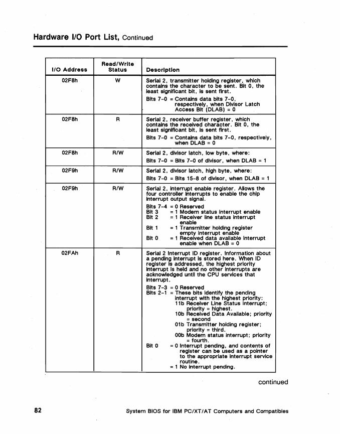
Hardware 1/0 Port List, Continued
I/O Address
02F8h
02F8h
02F8h
02F9h
02F9h
02FAh
Read/Write Status
W
R
R/W
R/W
R/W
R
Description
Serial 2. transmitter holding register. which contains the character to be sent. Bit O. the least significant bit. is sent first. Bits 7-0 =Contains data bits 7-0.
respectively. when Divisor Latch Access Bit (DLAB) =0
Serial 2. receiver buffer register. which contains the received character. Bit O. the least significant bit. Is sent first. Bits 7-0 =Contains data bits 7-0. respectively.
when DLAB =0
Serial 2. divisor latch. low byte. where: Bits 7-0 =Bits 7-0 of divisor. when DLAB =1
Serial 2. divisor latch. high byte. where: Bits 7-0 =Bits 15-8 of divisor. when DLAB =1
Serial 2. Interrupt enable register. Allows the four controller interrupts to enable the chip interrupt output signal. Bits 7-4 =0 Reserved Bit 3 =1 Modem status interrupt enable Bit 2 =1 Receiver line status interrupt
enable Bit 1 =1 Transmitter holding register
empty interrupt enable Bit 0 =1 Received data available interrupt
enable when DLAB =0
Serial 2 InterruptlD register. Information about a pending interrupt is stored here. When ID register is addressed. the highest priority interrupt is held and no other interrupts are acknowledged until the CPU services that interrupt. Bits 7-3 =0 Reserved Bits 2-1 =These bits identify the pending
interrupt with the highest priority: 11 b Receiver Line Status Interrupt;
priority =highest. 10b Received Data Available; priority
=second 01 b Transmitter holding register;
priority =third. OOb Modem status interrupt; priority
=fourth. Bit 0 =0 Interrupt pending. and contents of
register can be used as a pointer to the appropriate interrupt service routine.
=1 No interrupt pending.
continued
System BIOS for IBM PC/XT / AT Computers and Compatibles 82

Hardware 1/0 Port List, Continued
Read/Write I/O Address Status
02FBh R/W
02FCh R/W
Description
Serial 2, Line Control Register, where: Bit 7 =0 Receiver Buffer, Transmitter
Holding, or Interrupt Enable Registers Access
=1 Divisor Latch Access Bit 6 =1 Set Break Enabled. Serial output
Is forced to spacing state and remains there.
Bit 5 =Stick Parity Bit 4 =Even Parity Select Bit 3 =Parity Enable
=1 Even number of ones are sent and checked in the data word bits and parity bit. =0 Odd number of ones are sent and checked.
Bit 2 =Number of stop bits per character: =01 Stop bit =1 0 Stop bits
Bits 1-0 =Specify the number of bits per character: DDb 5 bit word length 01 b 6 bit word length 1Db 7 bit word length 11 b 8 bit word length
Serial 2, Modem Control Register. where: Bits 7-5 =0 Reserved Bit 4 =1 Loopback Mode for diagnostic
testing of serial port. Output of Transmitter Shift register Is looped back to Receiver Shift register Input. When in this mode, transmitted data is received immediately so that the CPU can verify the transmit data/ receive data serial port paths.
Bit 3 =1 Enable OUT2 Interrupt Bit 2 =1 Force OUT1 Active Bit 1 =1 Force Request To Send Active Bit 0 =1 Force Data Terminal Ready
Active
continued
I/O Port Addre.sses 83
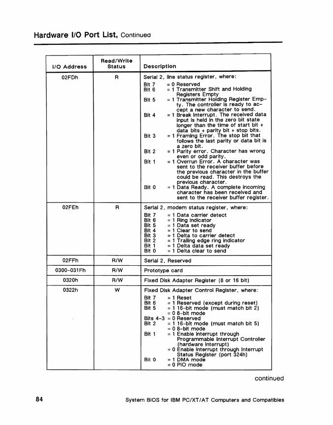
Hardware 1/0 Port List, Continuea
I/O Address
02FDh
02FEh
02FFh
0300-031Fh
0320h
0322h
Read/Write Status
R
R
R/W
R/W
R/W
W
Description
Serial 2, line status register, where:
Bit 7 =0 Reserved Bit 6 =1 Transmitter Shift and Holding
Registers Empty Bit 5 =1 Transmitter Holding Register Emp
ty. The controller is ready to accept a new character to send.
Bit 4 =1 Break Interrupt. The received data Input Is held in the zero bit state longer than the time of start bit + data bits + parity bit + stop bits.
Bit 3 =1 Framing Error. The stop bit that follows the last parity or data bit is a zero bit.
Bit 2 =1 Parity error. Character has wrong even or odd parity.
Bit 1 =1 Overrun Error. A character was sent to the receiver buffer before the previous character in the buffer could be read. This destroys the previous character.
Bit 0 =1 Data Ready. A complete Incoming character has been received and sent to the receiver buffer register.
Serial 2, modem status register, where:
Bit 7 =1 Data carrier detect Bit 6 =1 Ring indicator Bit 5 =1 Data set ready Bit 4 =1 Clear to send Bit 3 =1 Delta to carrier detect Bit 2 =1 Trailing edge ring indicator Bit 1 =1 Delta data set ready Bit 0 =1 Delta clear to send
Serial 2, Reserved
Prototype card
Fixed Disk Adapter Register (8 or 16 bit)
Fixed Disk Adapter Control Register, where:
Bit 7 =1 Reset Bit 6 =1 Reserved (except during reset) Bit 5 =1 16-blt mode (must match bit 2)
=0 8-bit mode Bits 4-3 =0 Reserved Bit 2 =1 16-bit mode (must match bit 5)
=0 8-bit mode Bit 1 =1 Enable interrupt through
Programmable Interrupt Controller (hardware Interrupt)
=0 Enable interrupt through Interrupt Status Register (port 324h)
Bit 0 =1 DMA mode =0 PIO mode
continued
System BIOS for IBM PC/XT/AT Computers and Compatibles 84
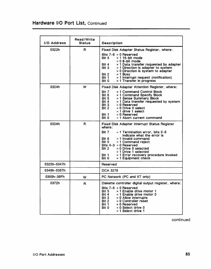
Hardware 1/0 Port List, Continued
I/O Address
0322h
0324h
0324h
0325h-0347h
0348h-0357h
0360h-36Fh
0372h
Read/Write Status
R
W
R
W
R
Description
Fixed Disk Adapter Status Register, where: Bits 7-6 =0 Reserved Bit 5 =1 16-blt mode
=0 8-blt mode Bit 4 =1 Data transfer requested by adapter Bit 3 =1 Direction Is adapter to system
=0 Direction Is system to adapter Bit 2 =1 Busy Bit 1 =1 Interrupt request (notification) Bit 0 =1 Transfer In progress
Fixed Disk Adapter Attention Register, where: Bit 7 =1 Command Control Block Bit 6 =1 Command Specify Block Bit 5 =1 Sense Summary Block Bit 4 =1 Data transfer requested by system Bit 3 =0 Reserved Bit 2 =0 Drive 0 select
=1 drive 1 select Bit 1 =0 Reserved Bit 0 =1 Abort current command
Fixed Disk Adapter Interrupt Status Register where: Bit 7
Bit 6 Bit 5 Bits 4-3 Bit 2
Bit 1 Bit 0
=1 Termination error, bits 0-6 indicate what the error is
=1 Invalid command = 1 Command reject =0 Reserved =0 Drive 0 selected =1 Drive 1 selected =1 Error recovery procedure invoked =1 Equipment check
Reserved
DCA 3278
PC Network (PC and XT only)
Diskette controller digital output register, where: Bits 7-6 =0 Reserved Bit 5 =1 Enable drive motor 1 Bit 4 =1 Enable drive motor 0 Bit 3 =0 Allow Interrupts Bit 2 =0 Controller reset Bit 1 =0 Reserved Bit 0 =0 Select drive 0
= 1 Select drive 1
continued
110 Port Addresses 85
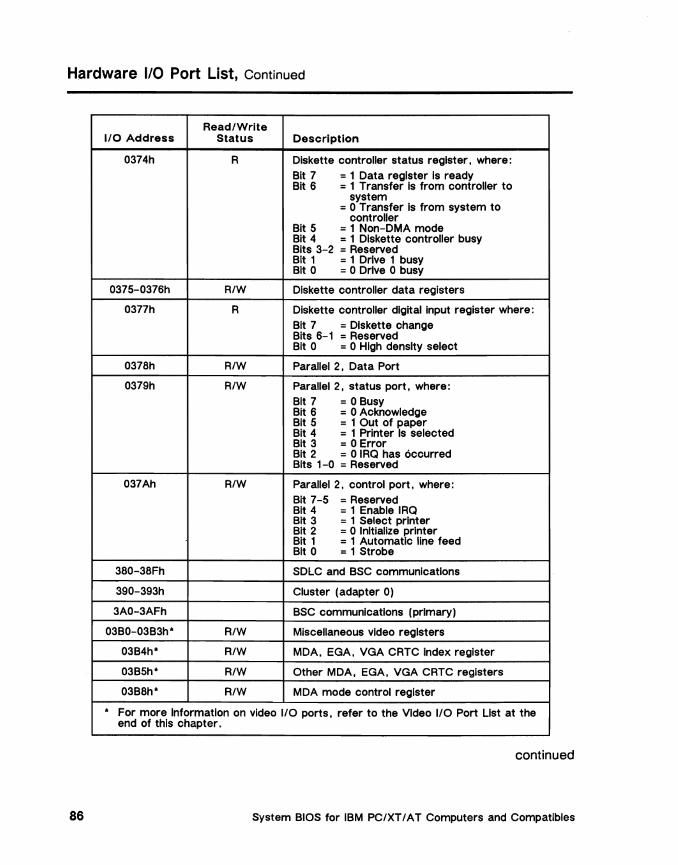
Hardware 1/0 Port List, Continued
I/O Address
0374h
0375-0376h
0377h
0378h
0379h
037Ah
380-38Fh
390-393h
3AO-3AFh
03BO-03B3h*
03B4h*
03B5h*
03B8h*
Read/Write Status
R
R/W
R
R/W
R/W
R/W
R/W
R/W
R/W
R/W
Description
Diskette controller status register, where: Bit 7 Bit 6
Bit 5 Bit 4 Bits 3-2 Bit 1 Bit 0
=1 Data register is ready =1 Transfer is from controller to
system =0 Transfer is from system to
controller =1 Non-DMA mode =1 Diskette controller busy =Reserved =1 Drive 1 busy =0 Drive 0 busy
Diskette controller data registers
Diskette controller digital input register where: Bit 7 =Diskette change Bits 6-1 =Reserved Bit 0 =0 High density select
Parallel 2, Data Port
Parallel 2, status port, where: Bit 7 Bit 6 Bit 5 Bit 4 Bit 3 Bit 2 Bits 1-0
=0 Busy =0 Acknowledge =1 Out of paper =1 Printer Is selected =0 Error =0 IRQ has occurred =Reserved
Parallel 2, control port, where: Bit 7-5 =Reserved Bit 4 =1 Enable IRQ Bit 3 =1 Select printer Bit 2 =0 Initialize printer Bit 1 =1 Automatic line feed Bit 0 =1 Strobe
SDLC and BSC communications
Cluster (adapter 0)
BSC communications (primary)
Miscellaneous video registers
MDA, EGA. VGA CRTC Index register
Other MDA, EGA. VGA CRTC registers
MDA mode control register
* For more Information on video I/O ports, refer to the Video 1/0 Port List at the end of this chapter.
continued
System BIOS for IBM PC/XT / AT Computers and Compatibles 86
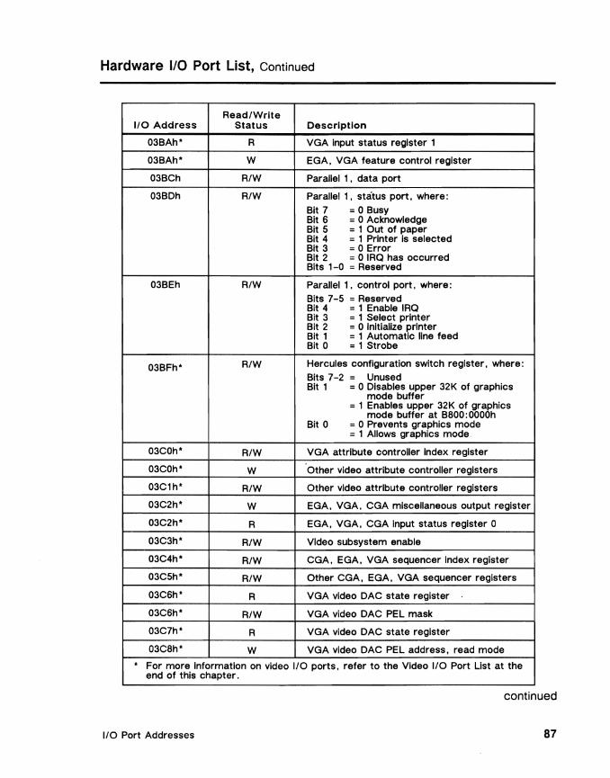
Hardware 1/0 Port List, Continued
I/O Address
03BAh*
03BAh*
03BCh
03BDh
03BEh
03BFh*
03COh*
03COh*
03C1h*
03C2h*
03C2h*
03C3h*
03C4h*
03C5h*
03C6h*
03C6h*
03C7h*
03C8h*
Read/Write Status
R
W
R/W
R/W
R/W
R/W
R/W
W
R/W
W
R
R/W
R/W
R/W
R
R/W
R
W
Description
VGA input status register 1
EGA. VGA feature controi register
Parallel 1. data port
Parallel 1. status port. where:
Bit 7 = 0 Busy Bit 6 = 0 Acknowledge Bit 5 = 1 Out of paper Bit 4 = 1 Printer is selected Bit 3 = 0 Error Bit 2 = 0 IRQ has occurred Bits 1-0 = Reserved
Parallel 1. control port. where: Bits 7...,5 = Reserved Bit 4 = 1 Enable IRQ Bit 3 = 1 Select printer Bit 2 = 0 Initialize printer Bit 1 = 1 Automatic line feed Bit 0 = 1 Strobe
Hercules configuration switch register. where: Bits 7-2 = Unused Bit 1 = 0 Disables upper 32K of graphics
mode buffer = 1 Enables upper 32K of graphics
mode buffer at B800: OOOOh Bit 0 = 0 Prevents graphics mode
= 1 Allows graphics mode
VGA attribute controller index register
Other video attribute controller registers
Other video attribute controller registers
EGA. VGA. CGA miscellaneous output register
EGA. VGA. CGA input status register 0
Video subsystem enable
CGA. EGA. VGA sequencer index register
Other CGA. EGA, VGA sequencer registers
VGA video DAC state register
VGA video DAC PEL mask
VGA video DAC state register
VGA video DAC PEL address, read mode
* For more information on video i/O ports, refer to the Video 1/0 Port List at the end of this chapter.
continued
I/O Port Addresses 87

Hardware 110 Port List, Continued
Read/Write 110 Address Status Description
03C8h* R/W VGA video DAC PEL address, write mode
03C9h* R/W VGA video DAC registers
03CAh* R/W CGA/EGA, VGA Graphics 2 position register
03CAh* R CGA/EGA, VGA feature control register
03CCh* VGA miscellaneous output register (R), VGA Graphics 1 position register (R/W) , EGA memory mode register (W)
03CDh* W VGA feature control register (color)
03CEh* R/W VGA graphics controller Index register
03CFh* W Other VGA graphics controller registers
03DOH* Video register
03D1h* Video register
03D2h* Video register
03D3h* Video register
03D4h* R/W Video CRTC Index register
03D5h* R/W Other CGA, EGA, VGA registers
03D6h* Video register
03D7h* Video register
03D8h* R/W CGA, EGA, VGA mode control register
03D9h* R/W CGA, EGA, VGA palette register
03DAh* CGA, EGA, VGA register
03DBh* Video register
03DCh* Video register
03DDh* Video register
03DEh* Video register
03DFh* Video register
03D4h* R VGA CRT controller index register (color)
03D5h* Other VGA CRT controller registers (color)
03DAh* R VGA input status register 1 (color)
03DAh* W VGA feature control register (color)
* For more Information on video I/O ports, refer to the Video I/O Port List at the end of this chapter.
continued
System BIOS for IBM PC/XT / AT Computers and Compatibles 88

Hardware 1/0 Port List, Continued
ReadlWrlte 1/0 Address Status Description
03FO!, R Diskette controller status register A. where: Bit 7 Bit 6 Bit S Bit 4 Bit 3 Bit 2 Bit 1 Bit 0
= 1 Interrupt pending = 0 Second drive installed =.1 Step = 1 Track 0 = 1 Head 1 select = 0 Index = 0 Wr-ite protect = 0 Data received by controller
03F1h R Diskette controller status register B. where: Bits 7-6 = 0 Reserved Bit S = Select drive Bit 4 = Write· data Bit 3 = Read data Bit 2 = Write enable Bit 1 = 1 Enable drive motor 1 Bit 0 = 1 Enable drive motor 0
03F2h W Diskette controller digital output register. where: Bits 7-6 = 0 Reserved Bit S == 1 Enable drive motor 1 Bit 4 = 1 Enable drive motor 0 Bit 3 = 0 Allow interrupts Bit 2 = 0 Controller reset Bit 1 = 0 Reserved Bit 0 = 0 Select drive 0
= 1 Select drive 1
03F4h R Diskette controller status register. where:
Bit 7 Bit 6
= 1 Data register is ready = 1 Transfer is from controller to
system = 0 Transfer is from system to
controller Bit S = 1 Non-DMA mode Bit 4 = 1 Diskette controller busy Bits 3-2 = Reserved Bit 1 = 1 Drive 1 busy Bit 0 = 0 Drive 0 busy
03FS-03F6h RIW Diskette controller data registers
continued
1/0 Port Addresses 89
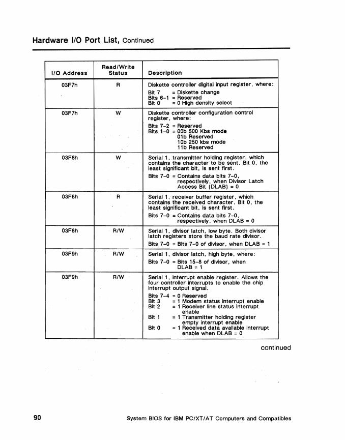
Hardware 1/0 Port List, Continued
Read/Write I/O Address Status Description
03F7h R Diskette controller digital Input register, where: Bit 7 Bits 6-1
=Diskette change =Reserved
Bit 0 =0 High density select
03F7h W Diskette controller configuration control register, where: Bits 7-2 =Reserved Bits 1-0 =OOb 500 Kbs mode
01 b Reserved 10b 250 kbs mode 11 b Reserved
03F8h W Serial 1,transmltter holding register, which contains the character to be sent. Bit 0, the least significant bit, Is sent first. Bits 7-0 =Contains data bits 7-0,
respectively, when Divisor Latch Access Bit (DLAB) =0
03F8h R Serial 1, receiver buffer register, which contains the received character. Bit 0, the least significant bit, Is sent first. Bits 7-0 =Contains data bits 7-0,
respectively, when DLAB =0
03F8h R/W Serial 1, divisor latch, low byte. Both divisor latch registers store the baud rate divisor. Bits 7-0 = Bits 7-0 of divisor, when DLAB = 1
03F9h R/W Serial 1, divisor latch, high byte, where: Bits 7-0 = Bits 15-8 of divisor, when
DLAEI = 1
03F9h R/W Serial 1, Interrupt. enable register. Allows the four controller interrupts to enable the chip interrupt output signal. Bits 7-4 = 0 Reserved Bit 3 Bit 2
=1 Modem status interrupt enable = 1 Receiver line status interrupt
enable Bit 1
Bit 0
=1 Transmitter holding register empty interrupt enable
=1 Received data available interrupt enable when DLAB = 0
continued
System BIOS for IBM PC/XT/AT Computers and Compatibles 90
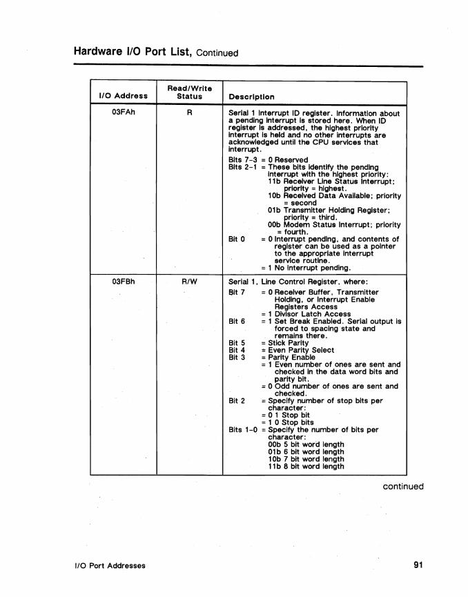
Hardware lID Port List, Continued
ReadlWrite 1/0 Address Status
03FAh R
03FBh RIW
Description
Serial 1 Interrupt ID register. Information about a pending Interrupt is stored here. When ID register Is addressed. the highest priority Interrupt Is held and no other interrupts are acknowledged until the CPU services that interrupt. Bits 7-3 =0 Reserved Bits 2-1 =These bits Identify the pending
Interrupt with the highest priority: 11 b Receiver Line Status Interrupt;
priority =highest. lOb Received Data Available; priority
=second 01 b Transmitter Holding Register;
priority = third. OOb Modem Status Interrupt; priority
= fourth. Bit 0 =0 Interrupt pending. and contents of
register can be used as a pointer to the appropriate interrupt service routine.
=1 No Interrupt pending.
Serial 1. Line Control Register. where:
ait 7 =0 Receiver Buffer. Transmitter Holding. or Interrupt Enable Registers Access
=1 Divisor Latch Access Bit 6 =1 Set Break Enabled. Serial output is
forced to spacing state and remains there.
Bit 5 =Stick Parity Bit 4 =Even Parity Select Bit 3 =Parity Enable
=1 Even number of ones are sent and checked in the data word bits and parity bit.
=0 Odd number of ones are sent and checked.
Bit 2 =Specify number of stop bits per character:
=0 1 Stop bit =1 0 Stop bits
Bits 1-0 =Specify the number of bits per character: OOb 5 bit word length 01 b 6 bit word length 1Ob 7 bit word length 11 b 8 bit word length
continued
1/0 Port Addresses 91
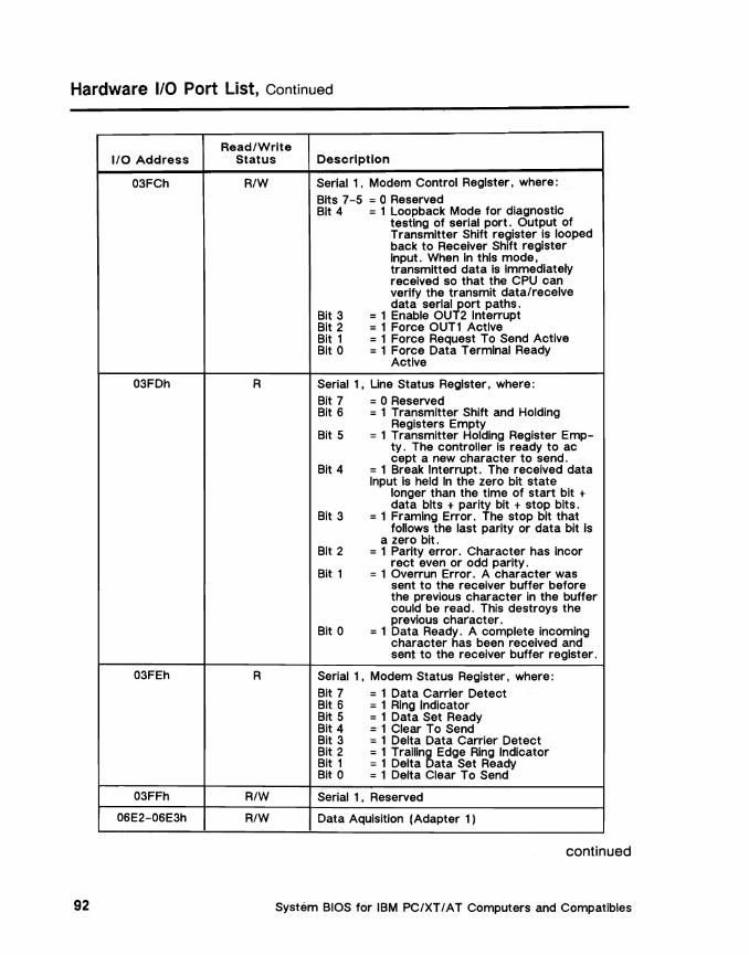
Hardware 1/0 Port List, Continued
Read/Write I/O Address Status Description
03FCh R/W Serial 1. Modem Control Register. where:
Bits 7-5 =0 Reserved Bit 4 =1 Loopback Mode for diagnostic
testing of serial port. Output of Transmitter Shift register is looped back to Receiver Shift register input. When in this mode. transmitted data is Immediately received so that the CPU can
Bit 3 Bit 2
verify the transmit data/receive data serial port paths.
=1 Enable OUT2 Interrupt =1 Force OUT1 Active
Bit 1 Bit 0
=1 Force Request To Send Active =1 Force Data Terminal Ready
Active
03FDh R Serial 1. Line Status Register. where: Bit 7 =0 Reserved Bit 6
Bit 5
Bit 4
=1 Transmitter Shift and Holding Registers Empty
=1 Transmitter Holding Register Empty. The controller is ready to ac cept a new character to send.
=1 Break Interrupt. The received data Input Is held In the zero bit state
longer than the time of start bit +
Bit 3 data bits + parity bit + stop bits.
=1 Framing Error. The stop bit that follows the last parity or data bit is
a zero bit. Bit 2
Bit 1
=1 Parity error. Character has inc or rect even or odd parity.
=1 Overrun Error. A character was sent to the receiver buffer before the previous character in the buffer could be read. This destroys the
Bit 0 previous character.
=1 Data Ready. A complete Incoming character has been received and sent to the receiver buffer register.
03FEh R Serial 1. Modem Status Register. where:
Bit 7 =1 Data Carrier Detect Bit 6 =1 Ring Indicator Bit 5 Bit 4
=1 Data Set Ready =1 Clear To Send
Bit 3 =1 Delta Data Carrier Detect Bit 2 Bit 1 Bit 0
=1 Trailing Edge Ring Indicator =1 Delta Data Set Ready =1 Delta Clear To Send
03FFh R/W Serial 1. Reserved
06E2-06E3h R/W Data Aquisitlon (Adapter 1)
continued
System BIOS for IBM PC/XT/AT Computers and Compatibles 92

Hardware 1/0 Port List, Continued
I/O Address
06E4-0790h
0790-0793h
0794-0AE1h
OAE2-0AE3h
OAE4-0BBFh
OB90-0B93h
OB94-13BFh
1390-1393h
1394-23BFh
2390-2393h
2394h-321Fh
3220h-3227h
322Bh-322Fh
3230h-42EOh
42E1h
42E2h-62EOh
62E1h
62E2h-B2EOh
B2E1h
B2E2h-A2EOh
A2E1h
A2E2h-C2EOh
A2E2h-AFFEh
AFFFh
BOOOh-C2EOh
C2E1h
C2E2h-E2EOh
E2E1h
E2E2h-FFFFh
Read/Write Status
R/W
R/W
R/W
R/W
R/W
R/W
R/W
R/W
R/W
R/W
R/W
R/W
R/W
R/W
Description
Reserved
Cluster (Adapter 1)
Reserved
Cluster (Adapter 2)
Reserved
Cluster (adapter 2)
Reserved
Cluster (adapter 3)
Reserved
Cluster (adapter 4)
Reserved
Serial Port 3 (see description for addresses 03FBh-03FFh for details).
Serial Port 4 (see description for addresses 03FBh-03FFh for details).
Reserved
GPIB (Adapter 2)
Reserved
GPIB (Adapter 3)
Reserved
GPIB (Adapter 4)
Reserved
GPIB (Adapter 5)
Reserved
Reserved
Plane 0-3 system latch (video register)
Reserved
GPIB (Adapter 6)
Reserved
GPIB (Adapter 7)
Reserved
110 Port Addresses 93

Video I/O Port List
Introduction
The following pages contain tables that describe ail the video I/O ports for each video adapter: MDA, CGA, EGA, and VGA. Because of the complexity of the way the video I/O ports are mapped, they are listed separately from the rest of the hardware I/O ports.
Table: MDA 1/0 ports
The 6845 CRTC's index register is mapped to I/O port 03B4h. The index value written to port 03B4h controls the register that appears at port 03B5h. The 6845 mode control register is accessed directly via I/O port 03B8h.
1/0 Address Read/Wrlte Index Description
03B4h R/W - CRTG Index Register
03B5h W 01h Horizontal Total
03B5h W 02h Horizontal Display Enable End
03B5h W 03h Start Horizontal Blanking
03B5h W 04h End Horizontal Blanking
03B5h W 05h Start Horizontal Retrace Pulse
03B5h W OSh End Horizontal Retrace
03B5h W 07h Vertical Total
03B5h W OSh Overflow
03B5h W 09h Preset Row Scan
03B5h W OAh Maximum Scan Line
03B5h W OAh Cursor Start
03B5h W OBh Cursor End
03B5h W OCh Start Address High
03B5h W ODh Start Address Low
03B5h R/W OEh Cursor Location High
03B5h R/W OFh Cursor Location Low
03B5h R/W 10h Light Pen High
03B5h R/W 11 h Light Pen Low
03BSh R/W - Mode Control Register
continued
System BIOS for IBM PC/XT IA T Computers and Compatibles 94

Video 1/0 Port List, Continued
Table: eGA 1/0 ports
The 6845 CRTC's index register is mapped to I/O port 03D4h. The value written to I/O port 03D4h controls the register that appears at port 03D5h. Mode control and palette registers are accessed via ports 03D8h and 03D9h.
I/O Address Read/Write
0304h R/W
0305h W
0305h W
0305h W
0305h W
03D5h W
03D5h W
03D5h W
0305h W
0305h W
0305h W
0305h W
0305h W
0305h W
0305h W
0305h R/W
0305h R/W
0305h R/W
0305h R/W
03D8h R/W
0309h R/W
Index
-
01h
02h
03h
04h
05h
06h
07h
08h
09h
OAh
OAh
OSh
OCh
OOh
OEh
OFh
10h
11h
--
Description
CRTC Index Register
Horizontal Total
Horizontal Display Enable End
Start Horizontal Blanking
End Horizontal Blanking
Start Horizontal Retrace Pulse
End Horizontal Retrace
Vertical Total
Overflow
Preset Row Scan
Maximum Scan Line
Cursor Start
Cursor End
Start Address High
Start Address Low
Cursor Location High
Cursor Location Low
Light Pen High
Light Pen Low
Mode Control Register
Palette Register
continued
I/O Port Addresses 95
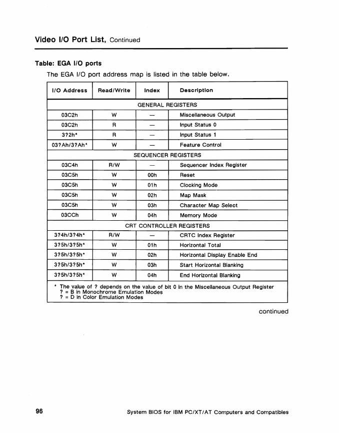
Video 1/0 Port List, Continued
Table: EGA 1/0 ports
The EGA lID port address map is listed in the table below.
I/O Address Read/Write Index Description
03C2h
03C2h
3?2h*
03?Ah/3?Ah*
03C4h
03C5h
03C5h
03C5h
03C5h
03CCh
3?4h/3?4h*
3?5h/3?5h*
3?5h/3?5h*
3?5h/3?5h*
3?5h/3?5h*
W
R
R
W
R/W
W
W
W
W
W
R/W
W
W
W
W
GENERAL REGISTERS
- Miscellaneous Output
- Input Status 0
- Input Status 1
- Feature Control
SEQUENCER REGISTERS
-OOh
01h
02h
03h
04h
Sequencer Index Register
Reset
Clocking Mode
Map Mask
Character Map Select
Memory Mode
CRT CONTROLLER REGISTERS
-
01h
02h
03h
04h
CRTC Index Register
Horizontal Total
Horizontal Display Enable End
Start Horizontal Blanking
End Horizontal Blanking
• The value of ? depends on the value of bit 0 In the Miscellaneous Output Register ? =B in Monochrome Emulation Modes ? =D in Color Emulation Modes
continued
System BIOS for IBM PC/XT I AT Computers and Compatibles 96
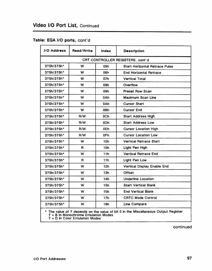
Video 1/0 Port List, Continued
Table: EGA 1/0 ports, cont'd
I/O Address Read/Write Index Description
CRT CONTROLLER REGISTERS, cont'd
3?5h/3?5h* W 05h Start Horizontal Retrace Pulse
3?5h/3?5h* W 06h End Horizontal Retrace
3?5h/3?5h* W 07h Vertical Total
3?5h/3?5h* W 08h Overflow
3?5h/3?5h* W 09h Preset Row Scan
3?5h/3?5h* W OAh Maximum Scan Line
3?5h/3?5h* W OAh Cursor Start
3?5h/3?5h* W OBh Cursor End
3?5h/3?5h* R/W OCh Start Address High
3?5h/3?5h* R/W ODh Start Address Low
3?5h/3?5h* R/W OEh Cursor Location High
3?5h/3?5h* R/W OFh Cursor Location Low
3?5h/3?5h* W 10h Vertical Retrace Start
3?5h/3?5h* R 10h Light Pen High
3?5h/3?5h* W 11 h Vertical Retrace End
3?5h/3?5h* R 11 h Light Pen Low
3?5h/3?5h* W 12h Vertical Display Enable End
3?5h/3?5h* W 13h Offset
3?5h/3?5h* W 14h Unqerline Location
3?5h/3?5h* W 15h Start Vertical Blank
3?5h/3?5h* W 16h End Vertiqal Blank
3?5h/3?5h* W 17h CRTC Mode Control
3?5h/3?5h* W 18h Line Compare
* The value of ? depends on the value of bit 0 in the Miscellaneous Output Register ? = B In Monochrome Emulation Modes ? = 0 in Color Emulation Modes
continued
110 Port Addre$ses 97
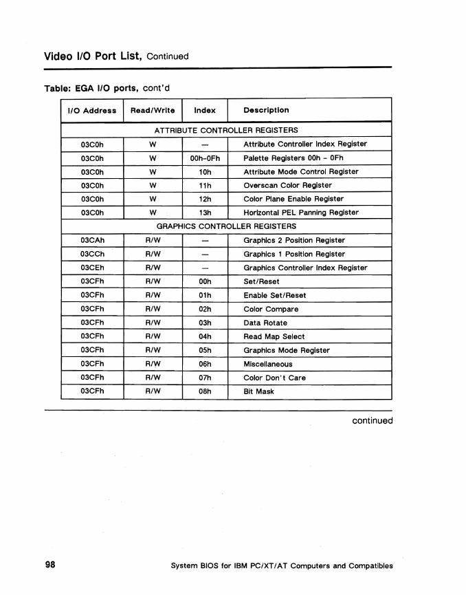
Video 1/0 Port List, Continued
Table: EGA 1/0 ports, cont'd
I/O Address
03COh
03COh
03COh
03COh
03COh
03COh
03CAh
03CCh
03CEh
03CFh
03CFh
03CFh
03CFh
03CFh
03CFh
03CFh
03CFh
03CFh
Read/Write Index Description
ATTRIBUTE CONTROLLER REGISTERS
W -W OOh-OFh
W 10h
W 11h
W 12h
W 13h
Attribute Controller Index Register
Palette Registers OOh - OFh
Attribute Mode Control Register
Overscan Color Register
Color Plane Enable Register
Horizontal PEL Panning Register
GRAPHICS CONTROLLER REGISTERS
R/W -R/W -R/W -
R/W OOh
R/W 01h
R/W 02h
R/W 03h
R/W 04h
R/W OSh
R/W 06h
R/W 07h
R/W 08h
Graphics 2 Position Register
Graphics 1 Position Register
Graphics Controller Index Register
Set/Reset
Enable Set/Reset
Color Compare
Data Rotate
Read Map Select
Graphics Mode Register
Miscellaneous
Co.lor Don't Care
Bit Mask
continued
System BIOS for IBM PC/XT / AT Computers and Compatibles 98
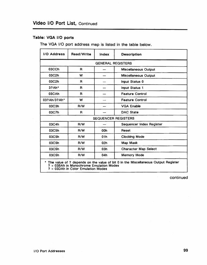
Video 1/0 Port List, Continued
Table: VGA 1/0 ports
The VGA I/O port address map is listed in the table below.
I/O Address Read/Write
03CCh
03C2h
03C2h
3?Ah*
03CAh
03?Ah/3?Ah*
03C3h
03C7h
R
W
R
R
R
W
R/W
R
03C4h
03C5h
03C5h
03C5h
03C5h
03C5h
R/W
R/W
R/W
R/W
R/W
R/W
Index Description
GENERAL REGISTERS
- Miscellaneous Output
- Miscellaneous Output
- Input Status 0
- Input Status 1
- Feature Control
- Feature Control
- VGA Enable
- DAC State
SEQUENCER REGISTERS
-OOh
01h
02h
03h
04h
Sequencer Index Register
Reset
Clocking Mode
Map Mask
Character Map Select
Memory Mode
• The value of ? depends on the value of bit 0 in the Miscellaneous Output Register ? = 03BAh in Monochrome Emulation Modes ? = 03DAh in Color Emulation Modes
continued
110 Port Addresses 99

Video 1/0 Port List, Continued
Table: VGA 1/0 ports. cont'd
1/0 Address Read/Wrlte Index Description
CRT CONTROLLER REGISTERS
3?4h/3?4h* R/W - CRTC Index Register
3?5h/3?5h* R/W 01h Horizontal Total
3?5h/3?5h* R/W 02h Hprlzontal Display Enable End
3?5h/3?5h* R/W 03h Start Horizontal Blanklrg
3?5h/3?5h* R/W 04h End Horizontal Blanking
3?5h/3?5h* R/W 05h Start Horizontal Retrace Pulse
3?5h/3?5h* R/W 06h End Horizontal Retrace
3?5h/3?5h* R/W 07h Vertical Total
3?5h/3?5h* R/W 08h Overflow
3?5h/3?5h* R/W 09h Preset Row Scan
3?5h/3?5h* R/W OAh Maximum Scan Line
3?5h/3?5h* R/W OAh Cursor Start
3?5h/3?5h* R/W OBh Cursor End
3?5h/3?5h* R/W OCh Start Address High
3?5h/3?5h* R/W ODh Start Address Low
3?5h/3?5h* R/W OEh Cursor Location High
3?5h/3?5h* R/W OFh Cursor Location Low
3?5h/3?5h* R/W 10h Vertical Retrace Start
3?5h/3?5h* R/W 11h Vertical Retrace End
3?5h/3?5h* R/W 12h Vertical Display Enable End
3?5h/3?5h* R/W 13h Offset
3?5h/3?5h* R/W 14h Underline Location
3?5h/3?5h* R/W 15h Start Vertical Blank
3?5h/3?5h* R/W 16h End Vertical Blank
3?5h/3?5h* R/W 17h CRTC Mode Control
3?5h/3?5h* R/W 18h Line Compare
* The value of ? depends on the value of bit 0 In the Miscellaneous Output Register ? " 03BAh in Monochrome Emulation Moc;tes ? = 03DAh in Color Emulation Modes
continued
System BIOS for IBM PC/XT I AT Computers and Compatibles 100
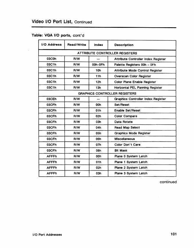
Video 110 Port List, Continued
Table: VGA I/O ports. cont'd
I/O Address
03COh
03C1h
03C1h
03C1h
03C1h
03C1h
03CEh
03CFh
03CFh
03CFh
03CFh
03CFh
03CFh
03CFh
03CFh
03CFh
AFFFh
AFFFh
AFFFh
AFFFh
Read/Write Index Description
ATTRIBUTE CONTROLLER REGISTERS
R/W -
R/W OOh-OFh
R/W 10h
R/W 11h
R/W 12h
R/W 13h
Attribute Controller Index Register
Palette Registers OOh - OFh
Attribute Mode Control Register
Overscan Color Register
Color Plane Enable Register
Horizontal PEL Panning Register
GRAPHICS CONTROLLER REGISTERS
R/W -R/W OOh
R/W 01h
R/W 02h
R/W 03h
R/W 04h
R/W OSh
R/W 06h
R/W 07h
R/W OSh
R/W OOh
R/W 01h
R/W 02h
R/W 03h
Graphics Controller Index Register
Set/Reset
Enable Set/Reset
Color Compare
Data Rotate
Read Map Select
Graphics Mode Register
Miscellaneous
Color Don' t Care
Bit Mask
Plane 0 System Latch
Plane 1 System Latch
Plane 2 System Latch
Plane 3 System Latch
continued
110 Port Addresses 101
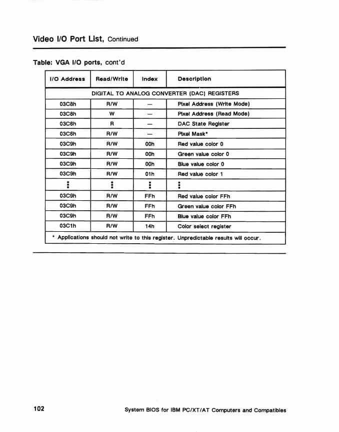
• • • • • •
• • • • • •
Video 1/0 Port List, Continued
Table: VGA 1/0 ports, cont'd
1/0 Address Read/Write Index Description
DIGITAL TO ANALOG CONVERTER (DAC) REGISTERS
03C8h R/W - Pixel Address (Write Mode)
03C8h W - Pixel Address (Read Mode)
03C6h R - DAC State Register
03C6h R/W - Pixel Mask"
03C9h R/W OOh Red value color 0
03C9h R/W OOh Green value color 0
03C9h R/W OOh Blue value color 0
03C9h R/W 01h Red value color 1
03C9h R/W FFh Red value color FFh
03C9h R/W FFh Green value color FFh
03C9h R/W FFh Blue value color FFh
03C1h R/W 14h Color select register
• Applications should not write to this register. Unpredictable results will occur.
System BIOS for IBM PC/XTIAT Computers and Compatibles 102

Chapter 6
Power-On Self Tests (POST)
Overview
Introduction
Before a computer system can be used, all system components must be tested and initialized, and the operating system must be bootstrapped into memory. The process of system test and initialization is generally under the control of the ROM BIOS. It is commonly referred to by the acronym POST, for power-on self test and initialization procedure.
IBM BIOS POST and Phoenix BIOS POST
The process followed in performing the power-on self test is similar in every XT or AT BIOS, although the POST process as described in this chapter applies more specifically to Phoenix BIOS products.
continued
Power-On Self Tests (POST) 103

Overview, Continued
How POST is started
The BIOS POST process can be started in any of the following ways:
Start Method BIOS Behavior
Apply power to system Jump to entry point indicated by the processor reset vector (I. e. turn system on.) (F:OOOOh). All POST tests and initializations are executed.
POST invokes BIOS INT 19h, Bootstrap Loader.
Reset system via Jump to entry point Indicated by the processor reset vecoptional hardware reset tor. All POST tests and initializations are executed. POST button. invokes BIOS INT 19h, Operating System Bootstrap Loader.
Press <Ctri> <Alt> <Del> INT 09h keyboard hardware Interrupt service routine trans(warm boot) fers control to BIOS POST. The POST test and Initialization
of memory above 64K Is not executed. All other POST tests and initiallzatlons are executed. POST Invokes BIOS INT 19h, Bootstrap Loader.
Processor reset vector location
The processor reset vector points to address FOOO:OOOOh.
In this chapter
This chapter presents the following information:
• POST Procedures
• Rules for Positioning liD Expansion ROM
• Re-Entering Real Mode (80286-based systems only)
• INT 19h, INT 18h, and System Boot
• POST Error Handling in AT Systems
• POST Error Handling in XT Systems
System BIOS for IBM PC/XT / A T Computers and Compatibles 104
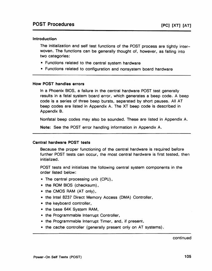
POST Procedures [PC] [XT] [AT]
Introduction
The initialization and self test functions of the POST process are tightly interwoven. The functions can be generally thought of, however, as falling into two categories:
• Functions related to the central system hardware
• Functions related to configuration and nonsystem board hardware
How POST handles errors
In a Phoenix BIOS, a failure in the central hardware POST test generally results in a fatal system board error, which generates a beep code. A beep code is a series of three beep bursts, separated by short pauses. All AT beep codes are listed in Appendix A. The XT beep code is described in Appendix B.
Nonfatal beep codes may also be sounded. These are listed in Appendix A.
Note: See the POST error handling information in Appendix A.
Central hardware POST tests
Because the proper functioning of the central hardware is required before further POST tests can occur, the most central hardware is first tested, then initialized.
POST tests and initializes the following central system components in the order listed below:
• The central processing unit (CPU),
• the ROM BIOS (checksum),
• the CMOS RAM (AT only),
• the Intel 8237 Direct Memory Access (OMA) Controller,
• the keyboard controller,
• the base 64K System RAM,
• the Programmable Interrupt Controller, • the Programmable Interrupt Timer, and, if present,
• the cache controller (generally present only on AT systems).
continued
Power-On Self Tests (POST) 105

POST Procedures, Continued [PC] [XT] [AT]
Nonsystem hardware POST tests
Once the central hardware has been tested and initialized, POST verifies that the system configuration data stored in CMOS RAM matches the actual hardware present. The remaining POST procedures test and initialize memory above 64K, the keyboard, the diskette and fixed disk drives, the CRT controller, and any nonsystem board hardware.
POST tests and initializes the following configuration and nonsystem board components in the order listed below:
• CMOS RAM configuration data,
• the CRT controllers,
• RAM memory above 64K,
• the keyboard,
• diskette drive A availability,
• the serial interface circuitry,
• the diskette controller,
• the fixed disk controller , and
• any additional hardware.
If an error occurs
A failure in the nonsystem hardware POST test generally results in a screen message. Both IBM and Phoenix AT BIOS messages are listed in Appendix A. XT BIOS messages are listed in Appendix B.
System BIOS for IBM PC/XTIAT Computers and Compatibles 106
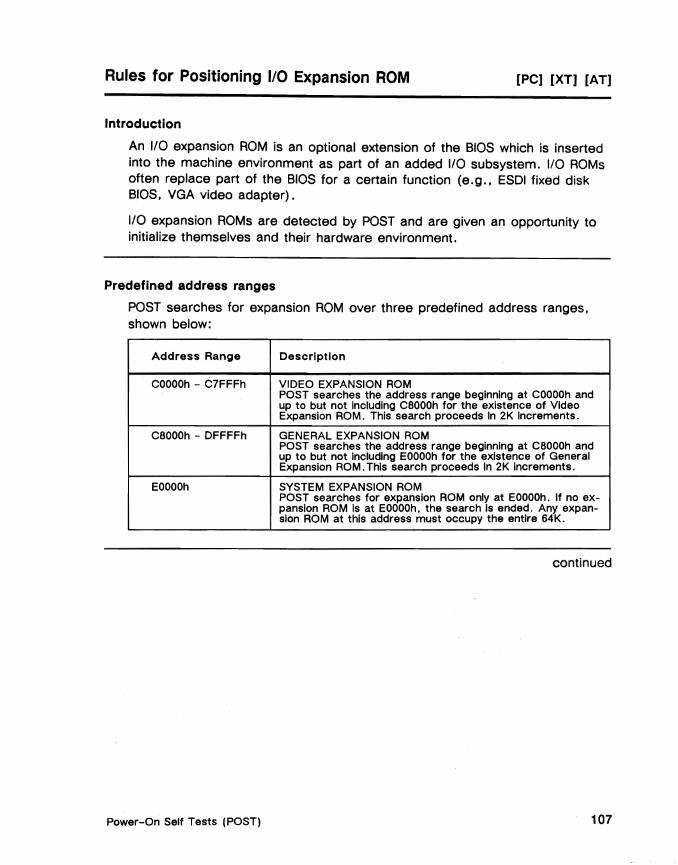
Rules for Positioning 1/0 Expansion ROM [PC] [XT] [AT]
Introduction
An 110 expansion ROM is an optional extension of the BIOS which is inserted into the machine environment as part of an added 1/0 subsystem. 1/0 ROMs often replace part of the BIOS for a certain function (e.g .• ESDI fixed disk BIOS. VGA video adapter).
1/0 expansion ROMs are detected by POST and are given an opportunity to initialize themselves and their hardware environment.
Predefined address ranges
POST searches for expansion ROM over three predefined address ranges. shown below:
Address Range Description
COOOOh - C7FFFh VIDEO EXPANSION ROM POST searches the address range beginning at COOOOh and up to but not Including C8000h for the existence of Video Expansion ROM. This search proceeds In 2K Increments.
C8000h - DFFFFh GENERAL EXPANSION ROM POST searches the address range beginning at C8000h and up to but not including EOOOOh for the existence of General Expansion ROM. This search proceeds In 2K increments.
EOOOOh SYSTEM EXPANSION ROM POST searches for expansion ROM only at EOOOOh. If no expansion ROM is at EOOOOh, the search Is ended. Any expansion ROM at this address must occupy the entire 64K.
continued
Power-On Self Tests (POST) 107
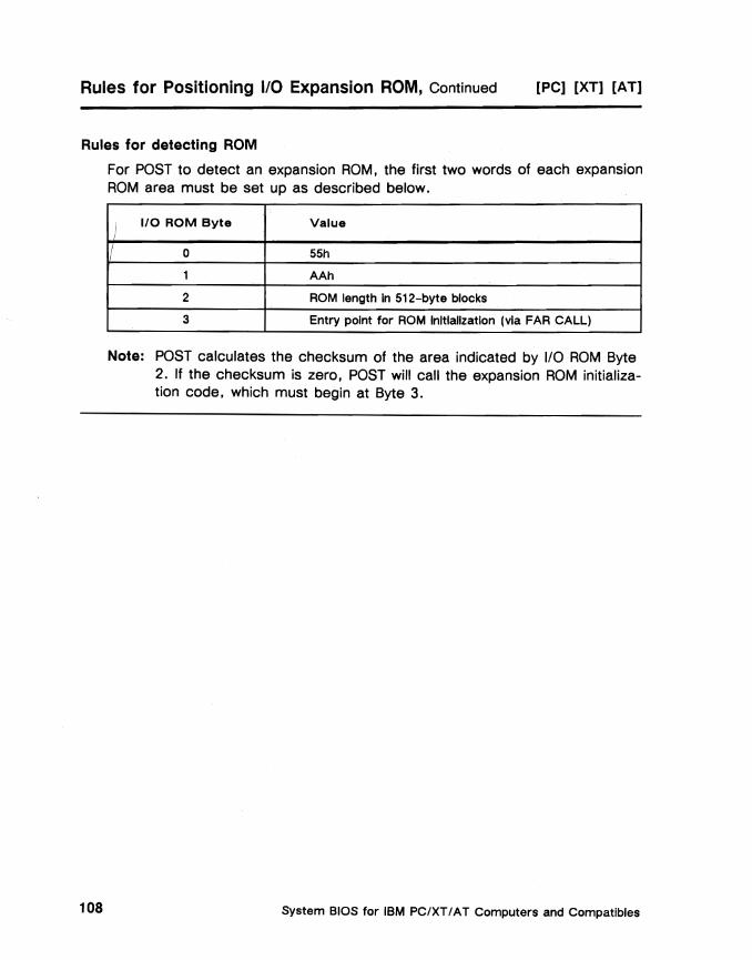
Rules for Positioning 1/0 Expansion ROM, Continued [PC] [XT] [AT]
Rules for detecting ROM
For POST to detect an expansion ROM, the first two words of each expansion ROM area must be set up as described below.
I·· , I/O ROM Byte Value
I 0 55h
1 AAh
2 ROM length In 512-byte blocks
3 Entry point for ROM Initialization (via FAR CALL)
Note: POST calculates the checksum of the area indicated by 1/0 ROM Byte 2. If the checksum is zero, POST will call the expansion ROM initialization code. which must begin at Byte 3.
System BIOS for IBM PC/XT I A T Computers and Compatibles 108
Re-Entering Real Mode (80286-based systems only) [AT]
Re-entry into real mode
Several POST processes require that the system be put into protected mode.
When returning to real mode from protected mode in an 80286-based systern, the processor is reset, therefore POST is re-entered. In order to prevent re-initialization of the system, POST reads the shutdown code stored in location OFh in CMOS RAM. It then jumps around the initialization procedures to the appropriate entry point.
Table of shutdown code values
As POST proceeds, it will use the shutdown codes with values 01 h, 02h, 03h, 04h, 06h, 07h, and 08h to return the processor to real mode.
Shutdown codes 05h and OAh are more flexible; they return control to the address stored in a double word pointer at 40:67h. These vectors are provided for use by operating system extensions such as 110 ROMs. Shutdown code 05h flushes the keyboard buffer and performs an end-of-interrupt (EOI) prior to vectoring. Shutdown code OAh simply vectors.
CMOS RAM Location Size Description
OFh 1 Byte SHUTDOWN CODE OOh = Power-on or sott reset 01h = Memory size pass 02h = Memory test pass 03h = Memory test tail 04h = POST end; boot system OSh = JMP dword pointer with end-ot-Interrupt 06h = Protected tests pass 07h = Protected tests tall OSh = Memory size tail 09h = INT 1Sh Block Move OAh = JMP dword pointer without end-at-interrupt
Power-On Self Tests (POST) 109
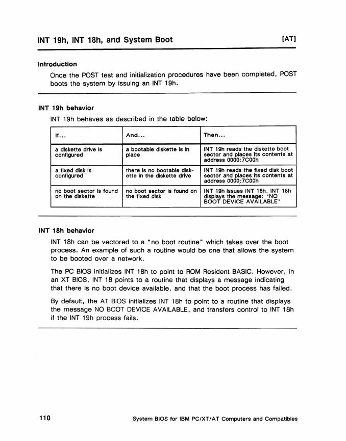
INT 19h, INT 18h, and System Boot [AT]
Introduction
Once the POST test and initialization procedures have been completed, POST boots the system by issuing an INT 19h.
INT 19h behavior
INT 19h behaves as described in the table below:
If ... And ... Then...
a diskette drive is a bootable diskette Is In . INT 19h reads the diskette boot configured place sector and places Its contents at
address 0000: 7COOh
a fixed disk Is there Is no bootable dlsk- INT 19h reads the fixed disk boot configured ette In the diskette drive sector and places Its contents at
address 000O,:7COOh
no boot sector Is found no boot sector Is found on INT 19h Issues INT 18h. INT 18h on the diskette the fixed disk displays the message: • NO
BOOT DEVICE AVAILABLE"
INT 18h behavior
INT 18h can be vectored to a .. no boot routine" which takes over the boot process. An example of such a routine would be one that allows the system to be booted over a network.
The PC BIOS initializes INT 18h to point to ROM Resident BASIC. However, in an XT BIOS, INT 18 points to a routine that displays a message indicating that there is no boot device available, and that the boot process has failed.
By default. the AT BIOS initializes INT 18h to point to a routine that displays the message NO BOOT DEVICE AVAILABLE, and transfers control to INT 18h if the INT 19h process fails.
System BIOS for IBM PC/XT / AT Computers and Compatibles 110
POST Error Handling in AT Systems [AT]
Introduction
For AT and AT-compatible systems. POST reports test or initialization failures in one of the following ways:
• Beep codes (only Phoenix BIOS products)
• System failure messages
• Boot failure messages • Informational messages
Reference
See Appendix A for a list of messages that can be generated by an AT BIOS. Separate lists are provided of Phoenix and IBM AT BIOS messages.
See Appendix B for a list of messages that can be generated by an XT BIOS. Separate lists are provided of Phoenix and IBM XT BIOS messages.
POST Error Handling in XT Systems [XT]
Introduction
For XT and XT-compatible systems. POST reports test or initialization failures in one of the following ways:
• Beep code • System failure messages
• Boot failure messages • Informational messages
Reference
See Appendix B for a more complete list of all messages that can be generated by a BIOS in an XT or XT-compatible system.
Power-Oli Self Tests (POST) 111

Chapter 7
INT 02h Nonmaskable Interrupt
Overview
Description
When the system hardware activates the Nonmaskable Interrupt (NMI) pin on the microprocessor, the BIOS INT 02h Nonmaskable Interrupt Service ISR is invoked. A nonmaskable interrupt is a hardware interrupt that cannot be masked. An NMI indicates a serious condition that usually cannot be shut off or diSabled by any process. The microprocessor does not generate an interrupt acknowledge cycle when it receives an NMI (as it usually does when it receives an interrupt), since the NMI is handled by a software ISR.
If an NMI is received while a previous NMI is being serviced, the second NMI is not serviced until the first has completed.
Disabling NMls
In AT systems, NMls can be disabled by setting bit 7 of the CMOS RAM address register port, 0070h. This practice is not recommended.
continued
INT 02h Nonmaskable Interrupt 113
Overview, Continued
In this chapter
This chapter describes the various NMI sources and tells how the BIOS Nonmaskable Interrupt ISR handles them.
The following topics are presented:
• XT NMI Handling
• 8087 Coprocessor Exceptions
• AT NMI Handling
• 80x87 Coprocessor Exceptions in AT Systems
How to determine level of support
Throughout this book, the commonly accepted level of support for each ROM BIOS function is identified by the legend [PC], [XT] , and/or [AT] on the same line as the function title.
Legend Description
[PC) Function Is supported by original IBM PC BIOS only.
tXT) Function is supported by all IBM PC/XT and compatible ROM BlOSs.
Note: This level of support Is contained In the ROM BIOS implemented in the majority of IBM PC and PC/XT compatible systems.
[AT) Function is supported by all IBM PCIAT and compatible ROM BlOSs.
System BIOS for IBM PC/XT /A T Computers and Compatibles 114

XT NMI Handling [XT]
XT BIOS Nonmaskable Interrupt ISR
When the system hardware activates the NMI pin on the 8086 or 8088 microprocessor, the XT BIOS INT 02h Nonmaskable Interrupt Service ISR is invoked.
The XT BIOS Nonmaskable Interrupt Service determines the reason for the NMI and takes appropriate action. In general, this involves:
• displaying a run-time error message (shown below), and
• halting the processor.
NMls can only be cleared by a system reboot. The BIOS supports NMI clearing by warm (Ctrl-Alt-Del) reboot or cold reboot (system reset button or power switch).
INT 02h vector
The XT BIOS initializes the INT 02h vector to FOOO:E2C3h. The INT 02h vector resides at address 00:08h in the BIOS interrupt vector table.
XT BIOS run-time error messages
The following messages may accompany an NMI in an XT system. Possible causes and solutions are listed. These messages apply only to systems with a Phoenix BIOS. Other BlOSs may generate different messages and may not let the user recover from the NMI without rebooting the system.
Message Possible Cause Solution
8087 NMI at address. An NMI occurred on access Type (S)hut off NMI. Type (S)hut off NMI, to the math coprocessor. Temporarily continues pro(R)eboot, other keys to cessing, but the coprocessorcontinue must be replaced.
Memory parity NMI at A memory chip(s) has Type (S)hut off NMI. address. Type (S)hut off failed. Temporarily continues pro-NMI, (R)eboot, other cessing. The bad memorykeys to continue chip(s) must be replaced.
liD card NMI at address. An NMI occurred on access Turn the machine off and Type (S)hut off NMI, to an adapter card. then on again. If that doesn't (R) eboot, other keys to work, replace the adapter continue card.
INT 02h Nonmaskable Interrupt 115

8087 Coprocessor Exceptions [XT]
Description
Systems based on the Intel 8086 and 8088 that incorporate the 8087 math coprocessor indicate math coprocessor exceptions by generating an NMI (i.e.,INT02h).
A user coprocessor exception routine should be written to handle 8087 coprocessor exceptions by intercepting INT 02h.
The coprocessor exception routine should determine if the NMI was generated by the 8087. If the NMI was not coprocessor related, the routine should transfer control to the BIOS NMI ISR. The graphic below illustrates the process that the caller's 8087 NMI handling routine must follow.
User 8087 Yes Coprocessor
Exception Exception Handler
No
BIOS 8087 NMI
ISR
System BIOS for IBM PC/XT I AT Computers and Compatibles 116
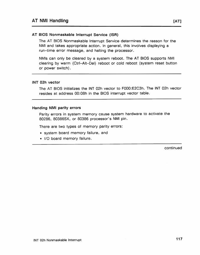
AT NMI Handling [AT]
AT BIOS Nonmaskable Interrupt Service (ISR)
The AT BIOS Nonmaskable Interrupt Service determines the reason for the NMI and takes appropriate action. In general, this involves displaying a run-time error message, and halting the processor.
NMls can only be cleared by a system reboot. The AT BIOS supports NMI clearing by warm (Ctrl-Alt-Del) reboot or cold reboot (system reset button or power switch).
INT 02h vector
The AT BIOS initializes the INT 02h vector to FOOO:E2C3h. The INT 02h vector resides at address 00:08h in the BIOS interrupt vector table.
Handing NMI parity errors
Parity errors in system memory cause system hardware to activate the 80286, 80386SX, or 80386 processor's NMI pin.
There are two types of memory parity errors:
• system board memory failure, and
• I/O board memory failure.
continued
INT 02h Nonmaskable Interrupt 117
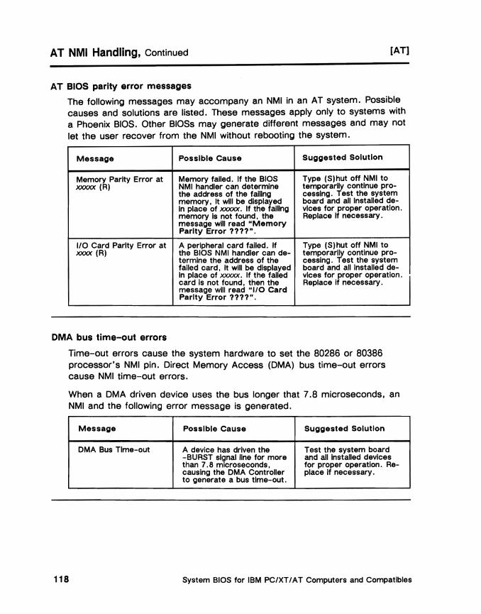
[AT]AT NMI Handling, Continued
AT BIOS parity error messages
The following messages may accompany an NMI in an AT system. Possible causes and solutions are listed. These messages apply only to systems with a Phoenix BIOS. Other BlOSs may generate different messages and may not let the user recover from the NMI without rebooting the system.
Message
Memory Parity Error at xxxxx (R)
I/O Card Parity Error at XXX)( (R)
DMA bus time-out errors
Possible Cause
Memory failed. If the BIOS NMI handler can determine the address of the failing memory. It will be displayed In place of xxxxx. If the failing memory Is not found. the message will read "Memory Parity Error ????".
A peripheral card failed. If the BIOS NMI handler can determine the address of the failed card. It will be displayed in place of xxxxx. If the failed card is not found. then the message will read "I/O Card Parity Error ???? H •
Suggested Solution
Type (S)hut off NMI to temporarily continue processlng. Test the system board and all Installed devices for proper operation. Replace If necessary.
Type (S)hut off NMI to temporarily continue processlng. Test the system board and all Installed devices for proper operation. Replace if necessary.
Time-out errors cause the system hardware to set the 80286 or 80386 processor's NMI pin. Direct Memory Access (DMA) bus time-out errors cause NMI time-out errors.
When a DMA driven device uses the bus longer that 7.8 microseconds, an NMI and the following error message is generated.
Message Possible Cause
DMA Bus Time-out A device has driven the -BURST signal line for more than 7.8 microseconds. causing the DMA Controller to generate a bus time-out.
Suggested Solution
Test the system board and all Installed devices for proper operation. Replace if necessary.
System BIOS for IBM PC/XT/AT Computers and Compatibles 118

SOxS7 Coprocessor Exceptions in AT Systems [AT]
80287/80387 coprocessor exceptions
Systems based on the 80286 or 80386 microprocessor that incorporate the 80287 or 80387 math coprocessor indicate math coprocessor exceptions by setting IRQ 13. IRQ 13 invokes INT 75h, the AT BIOS Coprocessor Exception Handling routine.
Software written to the 80287 or 80387 math coprocessor should handle coprocessor exceptions by intercepting INT 75h. The caller's coprocessor exception routine should determine if the NMI was generated by the 80287/ 80387 by following the process that is depicted in the graphic below. If the NMI was not coprocessor-related, the BIOS provides an INT 71 h handler which redirects coprocessor exceptions to INT 02h.
Applications80x87 Software
Exception Exception Handler
No
8087 Exception
AT BIOS NMI ISR
continued
INT 02h Nonmaskable Interrupt 119

80x87 Coprocessor Exceptions in AT Systems, Continued [AT]
How AT BIOS maintains compatibility
Unless it is revectored by a user program. the AT BIOS INT 75h Coprocessor Exception ISR is initialized to the same entry point as INT 02h. This ensures that 80x87 software running under AT BIOS is given the opportunity to handle coprocessor exceptions by intercepting INT 02h as it does in XT systems.
The AT BIOS initializes the INT 75h vector to FOOO:E2C3h (i.e .• the INT 02h entry point). The INT 75h vector resides at address OO:4Bh in the AT BIOS interrupt vector table.
XT compatibility
An AT-compatible system revectors any expansion bus hardware interrupt that generates an INT 02h in 8088-based systems to INT 71 h.
In an AT. hardware IRQ 9 generates an INT 71 h. The AT-compatible BIOS provides an interrupt handler which redirects this interrupt to INT OAh. providing compatibility with programs that expect the INT OAh interrupt handler in response to a hardware interrupt (8088-based systems).
System BIOS for IBM PC/XT I A T Computers and Compatibles 120
Chapter 8
INT 09h and INT 16h Keyboard Services
Overview
Introduction
The ROM BIOS contains two keyboard-related services, a Keyboard ISR and a Keyboard DSR:
• Keyboard ISR The BIOS Keyboard Interrupt Service routine (lSR) is invoked via hardware INT 09h each time a key is pressed. The BIOS Keyboard ISR processes keyboard data and converts it into information that is useful to the system. In most cases, this conversion results in the Keyboard ISR placing a two byte character code into a keystroke buffer located at 40: 1 Eh in low memory.
• Keyboard DSR The BIOS Keyboard Device Service routine (DSR) is invoked via software INT 16h. The BIOS Keyboard DSR provides an interface through which the operating system or application software can interface with the keystroke buffer. The Keyboard DSR contains functions that read the BIOS keyboard buffer, write to the buffer, return the status of the buffer, and so on.
continued
INT 09h and INT 16h Keyboard Services 121
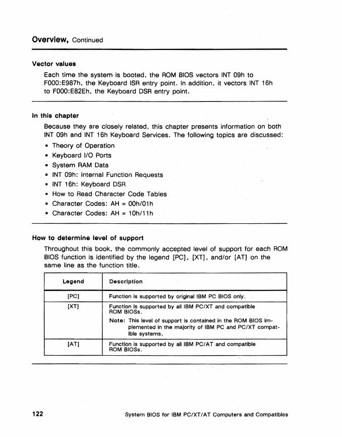
Overview, Continued
Vector values
Each time the system is booted, the ROM BIOS vectors INT 09h to FOOO:E987h, the Keyboard ISR entry point. In addition, it vectors INT 16h to FOOO:E82Eh, the Keyboard DSR entry point.
In this chapter
Becaus~ they are closely related, this chapter presents information on both INT 09h and INT 16h Keyboard Services. The following topics are dis~ussed:
• Theory of Operation
• Keyboard I/O Ports
• System RAM Data
• INT 09h: Internal Function Requests
• INT 16h: Keyboard DSR
• How to Read Character Code Tables
• Character Codes: AH = OOh/01 h
• Character Codes: AH = 10h/11h
How to determine level of support
Throughout this book, the commonly accepted level of support for each ROM BIOS function is identified by the legend [PC], [XT], and/or [AT] on the same line as the function title.
Legend Description
[PC] Function Is supported by original IBM PC BIOS only.
tXT] Function is supported by ali IBM PC/XT and compatible ROM BlOSs.
Note: This level of support is contained in the ROM BIOS implemented in the majority of IBM PC and PC/XT compatible systems.
[AT] Function is supported by ali IBM PC/AT and compatible ROM BlOSs.
System BIOS for IBM PC/XT/AT Computers and Compatibles 122

Theory of Operation
Introduction
IBM PC/XT, PCIAT, and compatible keyboards add flexibility to IBM compatible PCs by tying the interpretation of keystrokes to system software, rather than directly to keyboard hardware.
Raw key data originates in hardware
Each time a key is pressed or released, the IBM PC keyboard hardware generates a one byte .. make code" or .. break code."
The keyboard generates a key's make code each time that key is pressed, and it generates the key's break code each time the key is released. The byte associated with a key's break code is identical the one associated with its make code except that bit 7 is set. That is, the numeric value its break code is 80h higher than the key's make code.
Make and break code conversion
In and of itself, a key's make or break code has no direct meaning to an operating system or applications software. The keyboard make and break codes generated by a U.S keyboard, for example, are identical to the keyboard codes generated by a German, French, or Italian keyboard.
Keyboard codes are converted from meaningless numbers into ASCII characters or other meaningful data through a series of transformations controlled by system software. The number of transformations involved depends directlyon the kind of PC in use.
PC. PC/XT and the 8255A-5 controller chip
In IBM PC, PC/XT, and compatible systems, keyboard make and break -codes are converted from serial to parallel form by an Intel 8255A-5 (or compatible) keyboard controller chip. The 8255A-5 chip then generates an interrupt request (IRQ1) which invokes the ROM BIOS INT 09h Keyboard Interrupt Service Routine (ISR).
continued
INT 09h and INT 16h Keyboard Services 123

Theory of Operation, Continued
PC/AT and the 8042 controller chip
In IBM PC/AT and compatible systems. keyboard make and break codes are converted from serial to parallel form by an Intel 8042 (or compatible) keyboard controller chip.
Like its PC/XT counterpart, the 8042 chip generates IRQ1 which invokes the ROM BIOS INT 09h Keyboard Interrupt Service Routine. Because of hardware differences between PC and PC/AT keyboards, however, firmware resident in the 8042 controller must perform the additional step of converting AT key codes into System Scan Codes, values that are backwards compatible with those generated by PC/XT keyboards.
ROM BIOS INT 09h processing
The ROM BIOS Keyboard ISR analyzes each key code as follows:
• Codes generated by keyboard shift or toggle keys cause the Keyboard ISR to update the keyboard shift key and toggle key flags
• Shift key combinations, such as Ctrl-Alt-Del, Ctrl-Num Lock, and Ctrl Scroll Lock, are converted into requests for keyboard ISR internal functions, such as Reset, Pause, and Break.
• Codes that correspond to ASCII or special key values (e.g., function or edit keys) are converted into two byte character codes and are placed in a 16 word keystroke buffer. Operating systems or application software can then access the keystroke via the ROM BIOS INT16h Keyboard Device Service Routine (DSR).
Charact~r code format
The character codes generated by the INT 09h Keyboard ISR are made up of a low order byte. called the main byte, and of a high order byte. called the auxiliary byte. The ASCII value of a keystroke. if any, is always contained in the main byte; the auxiliary byte contains the keystroke's make code or system scan code. When a key, such as a function key, edit key, or function key combination, does not have an ASCII value, the Keyboard ISR sets the main byte to OOh and the auxiliary byte to a special key value.
Reference: A complete list of all character codes is found at the end of this chapter.
continued
System BIOS for IBM PC/XT I AT Computers and Compatibles 124
Theory of Operation, Continued
Typematic Rate and Delay
A key's break code indicates that the key has been released. The way the INT 09h ISR handles a key's break code depends on which key is pressed.
When a key is held down continuously, the keyboard hardware delays for a brief period then sends repeat values of the key's make code to the keyboard controller chip. Upon receipt of each make code, the controller chip does its processing and generates an IRQ1 which invokes INT 09h, the keyboard ISR.
If the make code corresponds to an alphanumeric, arrow, backspace, enter, or tab key, the keyboard ISR sends repeat character codes to the keystroke buffer until it receives the key's break code. If the make code corresponds to a special key, such as a function key, or a shift/toggle key, then the keyboard ISR ignores subsequent make codes from the keyboard, toggling the status of the key when it receives the key's break code.
INT 09h, DOS, and foreign keyboard support
The BIOS Keyboard ISR can only convert key codes into their American English ASCII values. When a foreign keyboard is in place, the MS-DOS command KEYBxx must be invoked. ("xx" must be a supported two-character country code) The KEYBxx command replaces the ROM BIOS INT 09h Keyboard ISR with one which uses foreign keyboard translation tables. For more information on foreign keyboards, refer to your PC-DOS or MS-DOS reference guide.
continued
INT 09h and INT 16h Keyboard Services 125
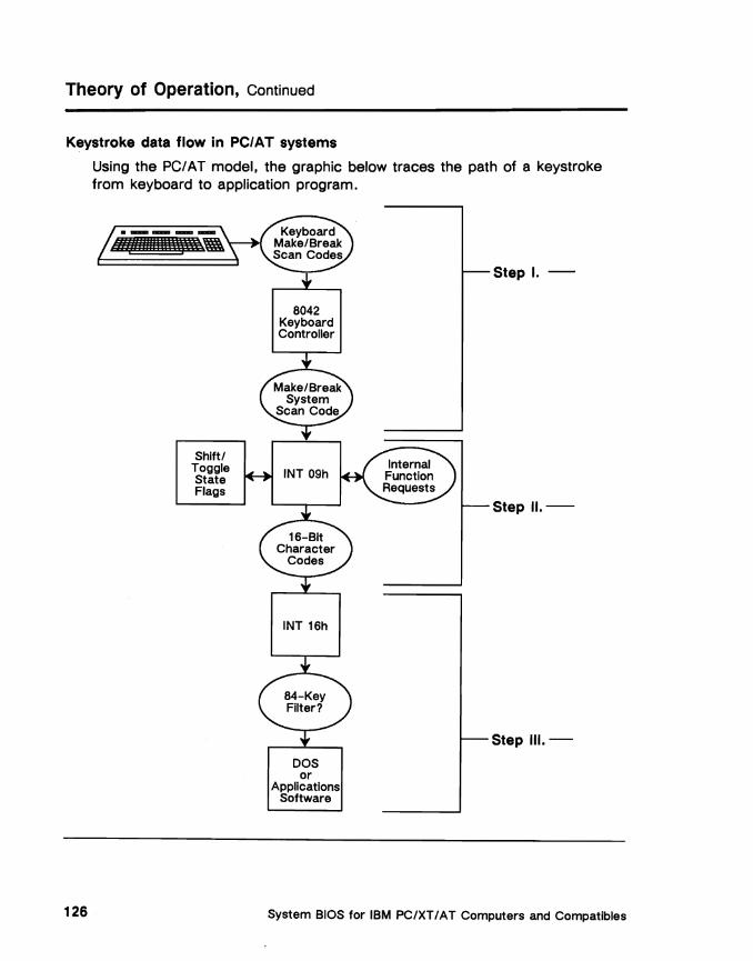
Theory of Operation, Continued
Keystroke data flow in PC/AT systems
Using the PC/AT model, the graphic below traces the path of a keystroke from keyboard to application program .
.__ .... : '
Step I. -
8042 Keyboard Controller
Shift I Toggle State Flags
Step 11.
INT 16h
Step 111.
DOS or
Applications Software
System BIOS for IBM PC/XT/AT Computers and Compatibles 126
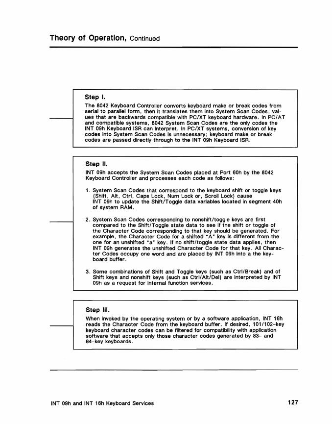
Theory of Operation, Continued
Step I. The 8042 Keyboard Controller converts keyboard make or break codes from serial to parallel form, then it translates them into System Scan Codes, values that are backwards compatible with PC/XT keyboard hardware. In PC/ A T and compatible systems, 8042 System Scan Codes are the only codes the INT 09h Keyboard ISR can Interpret. In PC/XT systems, conversion of key codes Into System Scan Codes is unnecessary; keyboard make or break codes are passed directly through to the INT 09h Keyboard ISR.
Step II. INT 09h accepts the System Scan Codes placed at Port 60h by the 8042 Keyboard Controller and processes each code as follows:
1. System Scan Codes that correspond to the keyboard shift or toggle keys (Shift, Alt, Ctrl, Caps Lock, Num Lock or, Scroll Lock) cause INT 09h to update the Shift/Toggle data variables located In segment 40h of system RAM.
2. System Scan Codes corresponding to nonshift/toggle keys are first compared to the Shift/Toggle state data to see If the shift or toggle of the Character Code corresponding to that key should be generated. For example, the Character Code for a shifted • A' key Is different from the one for an unshlfted • a" key. If no shift/toggle state data applies, then INT 09h generates the unshlfted Character Code for that key. All Character Codes occupy one word and are placed by INT 09h Into a the keyboard buffer.
3. Some combinations of Shift and Toggle keys (such as Ctrl/Break) and of Shift keys and nonshlft keys (such as Ctrl/Alt/Del) are interpreted by INT 09h as a request for Internal function services.
Step III. When Invoked by the operating system or by a software application, INT 16h reads the Character Code from the keyboard buffer. If desired, 101/102-key keyboard character codes can be filtered for compatibility with application software that accepts only those character codes generated by 83- and 84-key keyboards.
INT 09h and INT 16h Keyboard Services 127

Keyboard I/O Ports
INT 09h and 16h Keyboard Services reference the following 1/0 ports:
Read/Write I/O Address Status Description
0060h W Keyboard data Input buffer (AT-only)
0060h R Keyboard data output buffer (AT-only)
0062h W 8042 keyboard Input buffer (AT-only)
0061h R/W 8255 output register (XT -only), where:
Bit 7 = 1 Clear keyboard Bit 6 = 1 Hold keyboard clock low Bit 5 = 1 Enable 110 check Bit 4 = 1 Enable RAM parity check Bit 3 = 1 Read low switches Bit 2 = 0 Reserved Bit 1 = 1 Speaker data "enable Bit 0 = 1 Enable timer 2 gate to speaker
0062h R/W 8255 Input register (XT -only), where: Bit 7 Bit 6 Bit 5 Bit 4 Bit 3 Bit 2 Bit 1 Bit 0
= 1 RAM parity check = 1 1/0 channel check = 1 Timer channel 2 out = Reserved = 1 System board RAM size type 1 = 1 System board RAM size type 0 = 1 Coprocessor installed = 1 Loop In POST
0063h R/W 8255 Command mode register (XT -only) , where: Bits 7-6
Bits 5-4
Bits 3-2
= Number of diskette drives, where: OOb 1 drive 01b 2 drives lOb 3 drives llb 4 drives
= Type of display at power-on, where: OOb Reserved 01b 40x25 color (mono mode) lOb 80x25 color (mono mode) llb MDA (80x25)
= Memory on system board (256K chips), where:
OOb 256K 01b 5l2K lOb 576K llb 640K
Bits 3-2 = Memory on system board (64K chips), where:
OOb 64K 01b 128K lOb 192K l1b 256K
Bits 1-0 = Reserved
continued
System BIOS for IBM PC/XT I AT Computers and Compatibles 128

Keyboard 1/0 Ports, Continued
Read/Write I/O Address Status Description
0064h W 8042 keyboard Input buffer (AT-only)
0064h W 8042 Commands (AT-only)
0064h R 8042 Status (AT-only). where: Bit 7 Bit 6 Bit 5 Bit 4 Bit 3 Bit 2 Bit 1 Bit 0
System RAM Data
Introduction
=1 Parity error =1 General time out = 1 Auxiliary output buffer full =1 Inhibit switch =1 Command/data =System flag =1 Input buffer full =1 Output buffer full
Throughout the course of operation, the BIOS Keyboard Services monitor and maintain several status and buffer-control data definitions.
Keyboard data definitions
The keyboard data definitions, which are stored in segment 40h of the system RAM, are presented below in offset order.
Location Size Description
17h 1 Byte Keyboard shift flags. where: Bit 7 =1 Bit 6 =1 Bit 5 =1 Bit 4 =1 Bit 3 =1 Bit 2 =1 Bit 1 =1 Bit 0 = 1
Insert active Caps Lock active Num Lock active Scroll Lock active Alt pressed Ctrl pressed Left Shift pressed Right Shift pressed
continued
INT 09h and INT 16h Keyboard Services 129
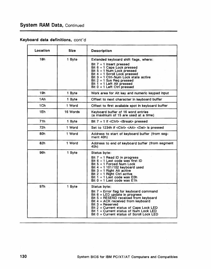
System RAM Data, Continued
Keyboard data definitions. cont'd
Location Size Description
18h 1 Byte Extended keyboard shift flags, where:
Bit 7 =1 Insert pressed Bit 6 =1 Caps Lock pressed Bit 5 =1 Num Lock pressed Bit 4 =1 Scroll Lock pressed Bit 3 =1 Ctrl-Num Lock state active Bit 2 =1 Sys Req pressed Bit 1 =1 Left Alt pressed Bit 0 =1 Left Ctrl pressed
19h 1 Byte Work area for Alt key and numeric keypad Input
1Ah 1 Byte Offset to next character In keyboard buffer
1Ch 1 Word Offset to first available spot In keyboard buffer
1Eh 16 Words Keyboard buffer of 16 word entries (a maximum of 15 are used at a time)
71h 1 Byte Bit 7 =1 If <Ctrl> <Break> pressed
72h 1 Word Set to 1234h If <Ctrl> <Alt> <Del> is pressed
80h 1 Word Address to start of keyboard buffer (from segment 40h)
82h 1 Word Address to end of keyboard buffer (from segment 40h)
96h 1 Byte Status byte: Bit 7 =1 Read 10 In progress Bit 6 =1 Last code was first 10 Bit 5 =1 Forced Num Lock Bit 4 =1 1 01 /1 02 keyboard used Bit 3 =1 Right Alt active Bit 2 =1 Right Ctrl active Bit 1 =1 Last code was EOh Bit 0 =1 Last code was E1h
97h 1 Byte Status byte: Bit 7 =Error flag for keyboard command Bit 6 =LED update In progress Bit 5 =RESEND received from keyboard Bit 4 =ACK received from keyboard Bit 3 =Reserved Bit 2 =Current status of Caps Lock LED Bit 1 =Current status of Num Lock LED Bit 0 =Current status of ScrOll Lock LED
System BIOS for IBM PC/XT / AT Computers and Compatibles 130
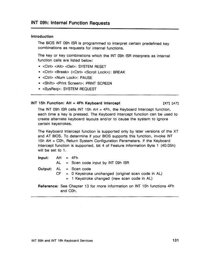
INT 09h: Internal Function Requests
Introduction
The BIOS INT 09h ISR is programmed to interpret certain predefined key combinations as requests for internal functions.
The key or key combinations which the INT 09h ISR interprets as internal function calls are listed below:
• <Ctrl> <Alt> <Del>: SYSTEM RESET
• <Ctrl> <Break> «Ctrl> <Scroll Lock»: BREAK
• <Ctrl> <Num Lock>: PAUSE
• <Shift> <Print Screen>: PRINT SCREEN
• <SysReq>: SYSTEM REQUEST
INT 15h Function: AH = 4Fh Keyboard Intercept [XT] [AT]
The INT 09h ISR calls INT 15h AH = 4Fh, the Keyboard Intercept function, each time a key is pressed. The Keyboard Intercept function can be used to create alternate keyboard layouts and/or to cause the system to ignore certain keystrokes.
The Keyboard Intercept function is supported only by later versions of the XT and AT BIOS. To determine if your BIOS supports this function, invoke INT 15h AH = COh, Return System Configuration Parameters. If the Keyboard Intercept function is supported. bit 4 of Feature Information Byte 1 (40:05h) will be set to 1.
Input: AH = 4Fh AL = Scan code input by INT 09h ISR
Output: AL = Scan code CF = o Keystroke unchanged (original scan code in AL)
= 1 Keystroke changed (new scan code in AL)
Reference: See Chapter 13 for more information on INT 15h functions 4Fh and COho
INT 09h and INT 16h Keyboard Services 131
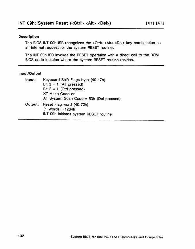
INT 09h: System Reset «Ctrl> <All> <Del» [XT] [AT]
Description
The BIOS INT 09h ISR recogflizes the <Ctrl> <Alt> <Del> key combination as an internal request for the system RESET routine.
The INT 09h ISR invokes the RESET operation with a direct call to the ROM BIOS code location where the system RESET routine resides.
Input/Output
Input: Keyboard Shift Flags byte (40: 17h) Bit 3 = 1 (Alt pressed) Bit 2 = 1 (Ctrl pressed) XT Make Code or AT System Scan Code = 53h (Del pressed)
Output: Reset Flag word (40:72h) (1 Word) = 1234h INT 09h initiates system RESET routine
System BIOS for IBM PC/XT I AT Computers and Compatibles 132

INT 09h: Break «Ctrl> <Break> or <Ctrl> <Scroll Lock» [XT] [AT]
Description
The BIOS INT 09h ISR recognizes the <Ctrl> <Break> key combination as an internal function request for INT 1 Bh. <Break> and <Scroll Lock> are equivalent keys on many keyboards.
INT 1Bh DSR is simply a vector which points to a body of programmercreated or application-program-resident code intended for execution when the <Ctrl> <Break> key combination is received from the keyboard.
Input/Output
Input: Keyboard Shift Flags byte (40: 17h): Bit 2 = 1 (Ctrl pressed) XT Make Code or AT System Scan Code = 46h (Break pressed)
Output: INT 09h invokes INT 1 Bh, a vector address which points to a break routine, if any.
INT 09h and INT 16h Keyboard Services 133
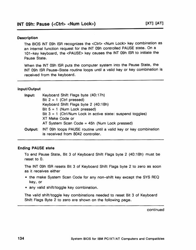
[XT] [AT]INT 09h: Pause «Ctrl> <Num Lock»
Description
The BIOS INT 09h ISR recognizes the <Ctrl> <Num Lock> key combination as an internal function request for the INT 09h controlled PAUSE state. On a 101-key keyboard. the <PAUSE> key causes the INT 09h ISR to initiate the Pause State.
When the INT 09h ISR puts the computer system into the Pause State. the INT 09h ISR Pause-State routine loops until a valid key or key combination is received from the keyboard.
Input/Output
Input: Keyboard Shift Flags byte (40: 17h) Bit 2 = 1 (Ctrl pressed) Keyboard Shift Flags byte 2 (40: 18h) Bit 5 = 1 (Num Lock pressed) Bit 3 = 1 (Ctrl/Num Lock in active state: suspend toggles) XT Make Code or AT System Scan Code = 45h (Num Lock pressed)
Output: INT 09h loops PAUSE routine until a valid key or key combination is received from 8042 controller.
Ending PAUSE state
To end Pause State. Bit 3 of Keyboard Shift Flags byte 2 (40: 18h) must be reset to O.
The INT 09h ISR resets Bit 3 of Keyboard Shift Flags byte 2 to zero as soon as it receives either
• the make System Scan Code for any non-shift key except the SYS REO key. or
• any valid shift/toggle key combination.
The valid shift/toggle key combinations needed to reset Bit 3 of Keyboard Shift Flags Byte 2 to zero are shown on the following page.
continued
System BIOS for IBM PC/XT / AT Computers and Compatibles 134

INT 09h: Pause «Ctrl> <Num Lock», Continued [XT] [AT]
PAUSE state table
The table below outlines the behavior of the various shift/toggle key combinations during the INT 09h Keyboard ISR pause state. The key combinations necessary to reset Bit 3 of Keyboard Shift Flags Byte 2 to zero (i.e., end Pause State) are in category #1 .
Shift Keys
None Shift (L or R)
2. 3. Alt Alt/Shift
Ctrl Ctrl/Shlft 4.
Alt/Ctrl Alt/CtrllShift 5.
LEGEND
1. PAUSE STATE IS ENDED (Bit 3 of Keyboard Shift Flags Byte 2 is reset). The scan codes normally associated with these keys do not have their usual effect on the shift and toggle flags. They are interpreted instead as a request to reset Bit 3 of Keyboard Shift Flags Byte 2 to zero, thus ending the Pause State.
2. PAUSE STATE IS NOT ENDED. The keyboard controller chip places the System Scan Code for (Ins) or (Shift Ins) into its internal buffer. The INT 09h ISR will act on these codes once Pause State is ended.
3. PAUSE STATE IS NOT ENDED. These key combinations are treated as valid requests to change Shift/Toggle states or update LEDs. (LED updating is supported on AT-compatible keyboards only.)
4. PAUSE STATE IS NOT ENDED. The keys which initiate the Pause State can not be used to end Pause State. When in Pause State, these keys are ignored.
5. PAUSE STATE IS NOT ENDED. When in Pause State, these keys are ignored.
INT 09h and INT 16h Keyboard Services 135

INT 09h: Print Screen «PrtSc> or <Shift> <PrtSc» [XT] [AT]
Description
The BIOS INT 09h ISR invokes INT OSh (the BIOS Print Screen service) whenever it receives the combination of System Make Scan Codes corresponding to the left or the right Shift key and the Print Screen key.
The System Make Scan Codes necessary to cause INT 09h to invoke INT OSh can be generated by pressing
• the Print Screen key alone. or
• either of the Shift keys and the Print Screen key.
Input/Output
Input Case #1: <PrtSc> key only
Input Case #2: <Shift> <PrtSc> keys
System Scan Codes = EOh. 2Ah. EOh. 37h (Left Shift and Print Screen both depressed)
Keyboard Shift Flags Byte (40: 17h) Bit 1 = 1 (Left Shift pressed) or Bit 0 = 2 (Right Shift pressed) System Scan Codes = EOh. 37h
Output for both Case #1 and Case #2:
INT 09h invokes INT OSh BIOS Print Screen Service
System BIOS for IBM PC/XT I AT Computers and Compatibles 136
INT 09h: System Request «SysReq» [AT]
Description
On AT-compatible systems. the BIOS INT 09h ISR interprets the System Request key in either of two ways:
• When the System Request key is depressed. INT 09h interprets the resulting System Scan Code as an internal function request for INT 15h: function AH = 85h. subfunction AL OOh - Process System Request.
• When the System Request key is released. INT 09h interprets the resulting System Scan Code as an internal request for INT 15h. function AH = 85h. subfunction AL = 01 h - Terminate System Request.
No.e: The Sys Req is not available on 83-key PC/XT and compatible keyboards.
Process SysReq input/output
The inputs and outputs that result when the System Request key is pressed are listed below:
Input: Keyboard Shift Flags Byte 2 (40:18h) Bit 2 = 1 (System Request pressed)
Output: AH = 85h AL = ~Oh INT 09h invokes INT 15h Process System Request
Terminate SysReq input/output
The inputs and outputs that result when the System Request key is released are listed below:
Input: Keyboard Shift Flags Byte 2 (40: 18h) Bit 2 = 0 (System Request key released)
Output: AH = 85h AL = 01 hiNT 09h invokes INT 15h Terminate System Request
INT 09h and INT 16h Keyboard Services 137

INT 16h: Keyboard DSR
Introduction
The BIOS Keyboard DSR is invoked via software interrupt INT 16h. Individual function codes are selected via the AH register.
Summary of INT 16h functions
A table of INT 16h AH register values and their corresponding function is shown below.
Function Description Platforms
OOh Read Keyboard Input [XT] [AT]
01h Return Keyboard Status [XT] [AT]
02h Return Shift Flag Status [XT] [AT]
03h Set Typematlc Rate and Delay [XT] [AT]
04h Reserved Reserved
OSh Store Key Data [XT] * [AT]
06h-OFh Reserved Reserved
10h Read Extended Keyboard Input [XT] * [AT]
11 h Return Extended Keyboard Status [XT] * [AT]
12h Return Extended Shift Flags Status [XT] * [AT]
13h-FFh Reserved Reserved
* Functions OSh and 10h - 12h are not supported on all XT BlOSs. See Determining level of support below.
Determining level of support
Functions 05h and 10h - 12h are not available on all XT BlOSs. To determine if your BIOS supports functions 05h and 10h - 12h;
• Use function 05h to write a value of FFFFh to the keyboard buffer. If function 05h returns with AL= OOh. the value was written and function 05h is supported. (See Function: AH = 05h Store Key Data in this chapter.)
• Use function 10h to read the keyboard buffer. If FFFFh is not returned in AX. retry at least 15 times (i.e. the buffer holds 16 characters). Functions 10h - 12h are supported only if FFFFh is returned to AX.
System BIOS for IBM PC/XT/AT Computers and Compatibles 138
INT 16h: AH = OOh Read Keyboard Input eXT] [AT]
Description
If a character code is available in the keyboard buffer, the Read Keyboard Input function reads the character code, removes it from the keyboard buffer, and returns its value in AX. The way this function processes when no character code is available depends on the kind of PC in place.
PC/XT processing
In PC/XT and compatible systems, if the keyboard buffer is empty, this function suspends program operation until a character code is inserted into the buffer. Users who wish to avoid suspending the system are advised to use function AH = 01 h Return Keyboard Status to test for the presence of a character code.
AT processing
In PC/AT and compatible systems, if the keyboard buffer is empty, this function invokes INT 15h function AH = 90h (Device Busy) with AL = 02h Keyboard. This allows the operating system to perform another task while the keyboard loop is occurring.
Once the INT 09h Keyboard ISR places a character code in the keyboard buffer, it invokes INT 15h function AH = 91 h (Interrupt Complete) with AL = 02h Keyboard. The Read Keyboard Input function then reads the character code, removes it from the buffer, and returns to the caller with the character code in AX. In addition, if the keyboard LEOs do not match the current flag settings, function AH = ~Oh also updates the keyboard LEOs.
Input/Output
Input: AH OOh
Output: AH Scan code or character 10 for special character AL = ASCII code or other translation of character.
Reference: The data table labeled" Character Codes: AH = 00h/01 h" lists the codes returned in AX when using INT 16h AH = OOh and AH=01h.
continued
INT 09h and INT 16h Keyboard Services 139
INT 16h: AH = OOh Read Keyboard Input, Continued [XT] [AT]
Extended key code "filtering"
The new and duplicate keys (i.e. the "extended keys") present on 101/102key PC/AT compatible keyboards generate System Scan Codes that are not useful to applications software written to interact exclusively with the traditional 83-key PC/XT or 84-key PC/AT keyboards.
The Read Keyboard Input function acts as an 83-key/84-key keyboard filter, selectively editing the keyboard buffer contents for 83-key/84-key keyboard compatibility. When a 1 01-key keyboard is in place, INT 16h function AH = OOh:
• returns all standard 83-key/84-key keyboard Character Codes as is,
• adjusts 1 01-key keyboard duplicate keyboard characters so that they take on the same two-byte key code as their 83-key/84-key counterparts, and
• destroys any 101-key Character Codes not compatible with the 83-key/ 84-key keyboards.
The "84th" key
"Sys Req," the 84th key on PC/AT compatible keyboards, is not present on PC/XT 83-key keyboards. The absence of this 84tH key is transparent to the Read Keyboard Input function; the System Scan Code generated by the Sys Req key is trapped by INT 09h and does not result in character code being placed in the keyboard buffer. For a discussion of INT 09h Sys Req key processing see "INT 09h: System Request <SysReq>" in this chapter.
Extended key passthrough
Function AH = 10h Read Extended Keyboard Input does not modify character codes for 84-key keyboard compatibility. For further details, see the Function: AH = 10h heading in this chapter.
System BIOS for IBM PC/XT I AT Computers and Compatibles 140
INT 16h: AH = 01h Return Keyboard Status [XT] [AT]
Description
This function is useful for allowing programs to check for keyboard input while continuing to run if there is none. It executes as follows:
• Checks to see if a two-byte character code is available in the keyboard buffer.
• If a key is waiting, a copy of the key is returned. The buffer is not incremented to the next key.
• If the keyboard buffer contains at least one key, the Zero Flag is cleared.
• If the keyboard buffer does not contain a key, the Zero Flag is set.
• In PCI AT systems, if the keyboard LEOs do not match the current flag settings, this function updates the LEOs.
Input/Output
Input: AH = 01h
Output: AH Scan code or character 10 for special character AL ASCII code or other translation of character. ZF 0 Character is ready
1 No character is available
Reference: The data table labeled" Character Codes: AH = 00h/01 h" lists the codes returned when using INT 16h AH = OOh and AH = 01 h.
Extended key code "filtering"
The new and duplicate keys (i. e. the "extended keys") present on 1 0 1 I 102-key PCI AT compatible keyboards generate System Scan Codes that are not useful to applications software written to interact exclusively with the traditional 83-key PC/XT or 84-key PCI AT keyboards.
The Read Keyboard Input function acts as an 83-key/84-key keyboard filter, selectively editing the keyboard buffer contents for 83-key/84-key keyboard compatibility.
Note: A complete discussion of extended key code filtering is found under the heading "INT 16h: AH = OOh Read Keyboard Input" on the previous page.
continued
INT 09h and INT 16h Keyboard Services 141

INT 16h: AH = 01 h Return Keyboard Status, Continued [XT] [AT]
Extended key passthrough
Function AH :: 11 h Return Extended Keyboard Status does not modify character codes for 84-key keyboard compatibility. For further details, see the Function: AH :: 11 h heading in this chapter.
INT 16h: AH = 02h Return Shift Flag Status [XT] [AT]
Description
The Return Shift Flag Status function returns the current shift status from the Keyboard Shift Flags byte (40: 17h).
Note: In PC/AT and compatible systems. the LED status is not updated.
Input/Output
Input: AH 02h
Output: AL Current shift status, where: Bit 7 :: 1 Insert active Bit 6 = 1 Caps Lock active Bit 5 :: 1 Num Lock active Bit 4 = 1 Scroll Lock active Bit 3 = 1 Alt pressed Bit 2 :: 1 Ctrl pressed Bit 1 = 1 Left Shift pressed Bit 0 = 1 Right Shift pressed
System BIOS for IBM PC/XTI AT Computers and Compatibles 142

INT 1Sh: AH = 03h Set Typematic Rate and Delay [AT]
Description
The Set Typematic Rate and Delay function changes the typematic rate (make code per second) and the delay (milliseconds before beginning typematic) .
Input/Output
If the parameters are valid. the function transmits a Set Rate command (F3h) to the keyboard controller.
Input: AH = 03h AL = 05h BH = Delay value (in milliseconds)
OOh =250 03h = 1000 01 h = 500 04h to FFh - Reserved 02h = 750
BL = Typematic rate (in characters per second) OOh =30.0 OBh = 10.9 16h =4.3 01h = 26.7 OCh = 10.0 17h = 4.0 02h = 24.0 ODh = 9.2 18h = 3.7 03h = 21.8 OEh = 8.6 19h =3.3 04h = 20.0 OFh = 8.0 1Ah =3.0 05h = 18.5 10h = 7.5 1Bh = 2.7 06h = 17.1 11h = 6.7 '1Ch = 2.5 07h = 16.0 12h = 6.0 1Dh = 2.3 08h = 15.0 13h = 5.5 1Eh = 2.1 09h = 13.3 14h = 5.0 1Fh =2.0 OAh = 12.0 15h = 4.6 20h to FFh - Reserved
Output: None
INT 1Sh: AH = 04h Reserved
INT 09h and INT 16h Keyboard Services 143
INT 16h: AH = OSh Store Key Data [XTI [AT]
Description
The Store Key Data function stores program-generated data into the keyboard buffer just as if a key were pressed. The buffer pointer (40: 1 Ch) is adjusted to point to the next available location in the keyboard buffer.
It the keyboard buffer is full, AL is set to indicate a keyboard buffer full error. Keyboard enhancers and other utilities can use this function to interpolate keys into the data stream viewed by applications ·programs.
XT support: This function is only supported by later version XT BlOSs. See Determining level of support under the heading INT 16h: Keyboard DSR.
Input/Output
Input: AH = OSh CH = Scan code CL = ASCII character
Output: AL OOh No error = 01 h Keyboard buffer full
INT 16h: AH = 06h - OFh Reserved
System BIOS for IBM PC/XT/AT Computers and Compatibles 144
INT 16h: AH = 10h Read Extended Keyboard Input [XT] [AT]
Description
The Read Extended Keyboard Input function reads the next two-byte character code in the keyboard buffer and returns the value in AX. It is designed for use with the 101/102-key keyboard. Unlike function AH = OOh, this function does not modify character codes for 84-key keyboard compatibility.
XT support: This function is only supported by later version XT BlOSs. See Determining level of support under the heading INT 16h: Keyboard DSR.
InputlOutput
Input: AH ::;: 10h
Output: AH ::;: Scan code or character ID for special character AL ::;: ASCII code or other translation of character
Reference: The character codes returned by this function are found in the table "Character Codes: AH = 10h/11h" in this chapter.
FOh low byte. filter
INT 09h places the value FOh in the low byte character code position for some Alt/character key combinations. The Return Extended Keyboard Input function strips FOh from the keyboard buffer image before returning to the caller. Keys with FOh are returned to AX with their low order byte set to OOh.
All other keys are returned to AX unmodified by this function.
Extended key "filtering"
Function AH ::;: OOh Read Keyboard Input selectively filters keyboard buffer input for compatibility with PC/XT 83-key and PC/AT 84-key keyboards. For details, see the Function: AH ::;: ~Oh heading in this chapter.
INT 09h and INT 16h Keyboard Services 145
INT 16h: AH = 11h Return Extended Keyboard Status [XT] [AT]
Description
This function is similar to function AH = 01 h, except that it returns unique scan codes for all keys on the 101 11 02-key keyboard. It executes as follows:
• Checks to see if a character code is available in the keyboard buffer.
• If a key is waiting, a copy of the character code is returned in AX. The buffer is not incremented to the next key.
• If the keyboard buffer contains at least one key, the Zero Flag is cleared.
• If the keyboard buffer does not contain a key, the Zero Flag is set.
• If the keyboard LEOs do not match the current flag settings, this function updates the LEOs.
XT support: This function is only supported by later version XT BlOSs. See Determining level of support under the heading INT 16h: Keyboard OSR.
Input/Output
Input: AH 11 h
Output: AH = Scan code or character 10 for special character (if ZF is set)
AL = ASCII code or other translation of character 10 (ZF is set) ZF = 0 No key in buffer
= 1 Key waiting
Reference: The character codes returned by this function are found in the table "Character Codes: AH = 10h/11h" in this chapter.
continued
System BIOS for IBM PC/XT I AT Computers and Compatibles 146

INT 16h: AH = 11h Return Extended Keyboard Status, Continued [XT] [AT]
FOh low byte filter
INT 09h places the value FOh in the low byte character code position of some Altlcharacter combinations. The Return Extended Keyboard Status function strips FOh from the keyboard buffer image before returning to the caller. Keys with FOh are returned to AX with their low order byte set to OOh. All other keys are returned to AX unmodified by this function.
Extended key "filtering"
Function AH = 01 h Read Keyboard Status selectively filters keyboard buffer input for compatibility with 84-key keyboards. For details. see" Function: AH = 01 h" in this chapter.
INT 16h: AH = 12h Return Extended Shift Flags Status [XT] [AT]
Description
This function is similar to function AH = 02h. except that it returns information on the shift keys provided on the 101/1 02-key keyboard. It also returns an additional byte of flags in the AH register.
The Return Extended Shift Flags Status function returns the shift flag status from Keyboard Shift Flags Byte (40: 17) in the AL register. and returns the shift flag status from Keyboard Shift Flags Byte 2 (40: 18) and 101-key Keyboard Status Byte (40:96) in the AH register.
XT support: This function is only supported by later version XT BlOSs. See Determining level of support under the heading INT 16h: Keyboard DSR.
continued
INT 09h and INT 16h Keyboard Services 147
INT 16h: AH = 12h Return Extended Shift Flags Status, Continued [XT] [AT]
Input/Output
Input: AH = 12h
Output: AH = More keyboard shift flags, where: Bit 7 = 1 Sys Req pressed (40: 18h Bit 2) Bit 6 = 1 Caps Lock active (40: 18h Bit 6) Bit 5 = 1 Num Lock active (40:18h Bit 5) Bit 4 = 1 Scroll Lock active (40: 18h Bit 4) Bit 3 = 1 Right Alt active (40:96h Bit 3) Bit 2 = 1 Right Ctrl active (40:96h Bit 2) Bit 1 = 1 Left Alt active (40: 18h Bit 1) Bit 0 = 1 Left Ctrl active (40: 18h Bit 0)
AL = Keyboard shift flags (copy of Keyboard Shift Flags Byte 40: 17), where: Bit 7 = 1 Insert active Bit 6 = 1 Caps Lock active Bit 5 = 1 Num Lock active Bit 4 = 1 Scroll Lock active Bit 3 = 1 Alt pressed Bit 2 = 1 Ctrl pressed Bit 1 = 1 Left Shift pressed Bit 0 = 1 Right Shift pressed
INT 16h: AH = 13h - FFh Reserved
Sy'stem BIOS for IBM PC/XT I A T Computers and Compatibles 148
How to Read Character Code Tables
Introduction
The tables on the following pages present data related to the IBM PC/XT / AT and compatible keyboards.
There are two character-code tables. They are labeled:
• Character Codes: AH = 00h/01 h
• Character Codes: AH = 1Oh/11 h
How to read the tables
• The data presented in each table is listed by key number and U. S. keyboard key legend. Readers who are using foreign keyboards should refer to the keyboard layout figures on the next page to see how their keyboard legend maps into key numbers.
• The columns labeled II Scan Codes" list the codes offered to the INT 09h ISR by the keyboard controller chip. In PC/AT compatible systems these codes are generated by the 8042 controller chip and are more commonly referred to as System Scan Codes. Only Make Code values are listed. Break codes are found by adding a value of 80h to the make code in question. Scan Codes in EO-xxh form correspond to the 101l102-key keyboard extended keys. These keys are not present on 83- and 84-key keyboards.
• The two-byte number associated with each Character Code is listed in four-digit hex notation. The high order byte, which is placed by INT 16h into the AH register, is listed first. The low order byte, which is placed by INT 16h into the AL register, is listed second. The two bytes are separated with a slash. For example, the Character Code for the unshifted lin" key is listed on the table as 31/6E.
• Caps Lock plus any typewriter key yields the same character code as Shift plus any typewriter key.
• Num Lock plus any numeric keypad key yields the same character code as Shift plus any numeric keypad key.
• Alt plus the decimal value for an ASCII character input from the numeric keypad yields the ASCII character. Allowable values are 0 to 255. These instances are noted with II •• " in the Alt column.
continued
INT 09h and INT 16h Keyboard Services 149

How to Read Character Code Tables, Continued
83-key, 84-key, and 101/1 02-key keyboard numbers
The key number systems applied to 83-key PC-compatible, 84-key ATcompatible, and 101f.l02-key AT-compatible keyboards are shown below.
83-Key Keyboard
59 60 69 70
61 62 27 71 72 73 74
~__"~JL~~~~~..JL~~.-~~..JL~~~~~-t 28
63 64 41 75 76 77
65 66 42 54 55 79 80 81 78
67 68 82 83
84-Key Keyboard
70 65 90 95 100 lOS
71 66 ., •• 101 106
72 67 92 97 102 107
73 68 93 98 103
108
74 69 99 104
75 80 86 90 95 100 lOS
76 81 8. 91 96 101
106
92 97 102
~ 93 98 103
c:EEl 99 104
108
System BIOS for IBM PC/XTI AT Computers and Compatibles 150
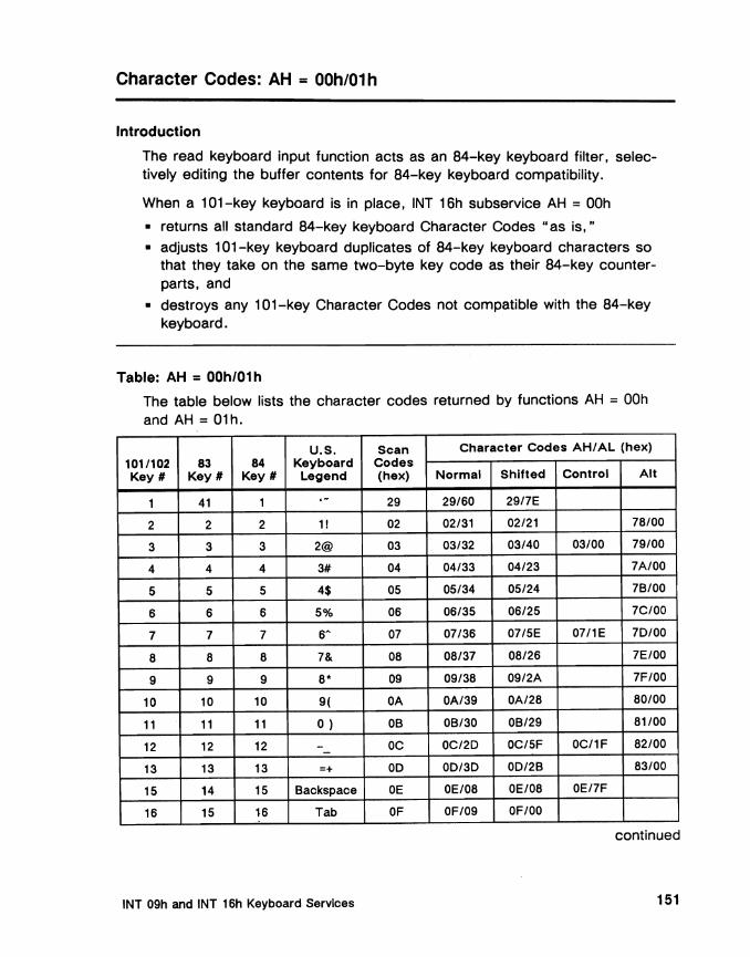
Character Codes: AH = OOh/01 h
Introduction
The read keyboard input function acts as an 84-key keyboard filter, selectively editing the buffer contents for 84-key keyboard compatibility.
When a 1 01-key keyboard is in place, INT 16h subservice AH = OOh
• returns all standard 84-key keyboard Character Codes "as is,"
• adjusts 1 01-key keyboard duplicates of 84-key keyboard characters so that they take on the same two-byte key code as their 84-key counterparts, and
• destroys any 101-key Character Codes not compatible with the 84-key keyboard.
Table: AH = OOh/01 h
The table below lists the character codes returned by functions AH = OOh and AH = 01h.
u.s. Scan Character Codes AHIAL (hex) 101/102 83 84 Keyboard Codes Key # Key # Key # Legend (hex) Normal Shifted Control Alt
1 41 1 , 29 29/60 29/7E
2 2 2 1! 02 02/31 02/21 78/00
3 3 3 2@ 03 03/32 03/40 03/00 79/00
4 4 4 3# 04 04/33 04/23 7A/00
5 5 5 4$ 05 05/34 05/24 7B/00
6 6 6 5% 06 06/35 06/25 7C/00
7 7 7 6A 07 07/36 07/5E 07/1 E 70/00
8 8 8 7& 08 08/37 08/26 7E/00
9 9 9 8" 09 09/38 09/2A 7F/00
10 10 10 9( OA OA/39 OA/28 80/00
11 11 11 o ) OB OB/30 OB/29 81/00
12 12 12 -- OC OC/20 OC/5F OCllF 82/00
13 13 13 =+ 00 00/30 OOI2B 83/00
15 14 15 Backspace OE OE/08 OE/08 OE/7F
16 15 16 Tab OF OF/09 OFIOO
continued
INT 09h and INT 16h Keyboard Services 151

Character Codes: AH = OOh/01 h, Continued
Table: AH = OOh/01h, cont'd
Character Codes AH/AL (hex) 101/102 83 84 Keyboard Codes Key # Key # Key # Legend (hex) Normal Shifted Control Alt
17 16 17 Q 10 10/71 10/51 10/11 10/00
18 17 18 W 11 11/77 11/57 11/17 11/00
19 18 19 E 12 12/65 12/45 12/05 12/00
20 19 20 R 13 13/72 13/52 13/12 13/00
21 20 21 T 14 14/74 14/54 14/14 14/00
22 21 22 Y 15 15/79 15/59 15/19 15/00
23 22 23 U 16 16/75 16/55 16/15 16/00
24 23 24 I 17 17/69 17/49 17109 17100
25 24 25 0 18 18/6F 18/4F 18/0F 18/00
26 25 26 P 19 19/70 19/50 19/10 19/00
27 26 27 [ { 1A 1A/5B 1A/7B 1A/1B
28 27 28 I } 1B 1B/5D 1B/7D 1B/1D
29' 43 14 : \ 2B 2B/5C 2B/7C 2B/1C
30 58 64 Caps Lock 3A
31 30 31 A 1E 1E/61 1E/41 1E/01 1E/00
32 31 32 S 1F 1F/73 1F/53 1F/13 1F/OO
33 32 33 D 20 20/64 20/44 20104 20100
34 33 34 F 21 21/66 21/46 21/06 21/00
35 34 35 G 22 22/67 22/47 22/07 22/00
36 35 36 H 23 23/68 23/48 23/08 23/00
37 36 37 J 24 24/6A 24/4A 24/0A 24/00
38 37 38 K 25 25/6B 25/4B 25/0B 25/00
39 38 39 L 26 26/6C 26/4C 26/0C 26/00
40 39 40 , . 27 27/3B 27/3A
U.S. Scan
' .41 40 41 28 28/27 28/22
42 (102-key 2B 2B/5C 2B/7C 2B/1Conly)
43 28 43 Enter~ 1C 1C/OD 1C/OD 1C/OA
, 101-key keyboard only.
continued
152 System BIOS for IBM PC/XT I A T Computers and Compatibles
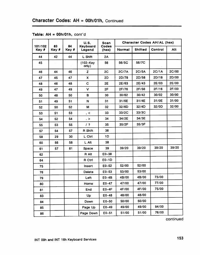
Character Codes: AH = OOh/01 h, Continued
Table: AH = OOh/01 h, cont'd
101/102 Key #
83 Key #
84 Key #
U.S. Keyboard Legend
Scan Codes (hex)
Character Codes AHIAL (hex)
Normal Shifted Control Alt
44 42 44 L Shift 2A
45 (102-Keyonly)
56 56/5C 56/7C
46 44 46 Z 2C 2C/7A 2C/5A 2C/1A 2C/00
47 45 47 X 2D 2D/78 2D/58 2D/18 2D/00
48 46 48 C 2E 2E/63 2E/43 2E/03 2E/OO
49 47 49 V 2F 2F/76 2F/56 2F/16 2F/00
50 48 50 B 30 30/62 30/42 30/02 30/00
51 49 51 N 31 31/6E 31/4E 31/0E 31/00
52 50 52 M 32 32/6D 32/4D 32/0D 32/00
53 51 53 ,< 33 33/2C 33/3C
54 52 54 .> 34 34/2E 34/3E
55 53 55 I ? 35 35/2F 35/3F
57 54 57 R Shift 36
58 29 30 L Ctrl 1D
60 56 58 L Alt 38
61 57 61 Space 39 39/20 39/20 39/20 39/20
62 R Alt EO-38
64 R Ctrl EO-1D
75 Insert EO-52 52/00 52/00
76 Delete EO-53 53/00 53/00
79 Left EO-4B 4B/00 4B/00 73/00
80 Home EO-47 47/00 47100 77100
81 End EO-4F 4F/00 4F/00 75/00
83 Up EO-48 48/00 48/00
84 Down EO-50 50/00 50/00
85 Page Up EO-49 49/00 49/00 84/00
86 Page Down EO-51 51100 51100 76/00
continued
INT 09h and INT 16h Keyboard Services 153
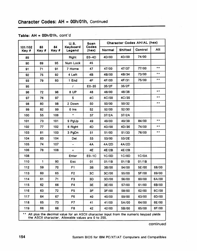
••
Character Codes: AH = OOh/01 h, Continued
Table: AH = OOh/01h, cont'd
Character Codes AHIAL (hex)U.S. Scan 101/102 83 84 Keyboard Codes Key # Key # Key # Legend (hex) Normal Shifted Control Ait
89 Right EO-40 40/00 40/00 74/00
90 69 95 Num Lock 45
91 71 91 7 Home 47 47/00 47/37 77/00
92 75 92 4 Left 4B 4B/00 4B/34 73/00 •• ..93 79 93 1 End 4F 4F/00 4F/31 75/00
95 / EO-35 35/2F 35/2F
96 72 96 8 UP 48 48/00 48/38 ••
97 76 97 5 4C 4C/00 4C/35 ••
98 80 98 2 Down 50 50100 50/32 ••
99 82 99 o Ins 52 52/00 52/30
100 55 106 • 37 37/2A 37/2A
101 73 101 9 PgUp 49 49/00 49/39 84/00 ••
102 77 102 6 Right 40 40/00 40/36 74/00 •• 103 81 103 3 pgOn 51 51/00 51133 76/00 ••
104 83 104 Del 53 53/00 53/2E
105 74 107 - 4A 4A/20 4A/20
106 78 108 + 4E 4E/2B 4E/2B
108 Enter EO-1C 1C/00 1C/00 1C/OA
110 1 90 Esc 01 01/18 01/1B 01/1 B
112 59 70 F1 3B 38/00 54/00 5E/00 68/00
113 60 65 F2 3C 3C/00 55/00 5F/00 69/00
114 61 71 F3 3D 30/00 56/00 60100 6A/00
115 62 66 F4 3E 3E/00 57/00 61/00 6B/00
116 63 72 F5 3F 3F/00 58/00 62/00 6C/00
117 64 67 F6 40 40/00 59/00 63/00 60/00
118 ·65 73 F7 41 41/00 5A/00 64/00 6E/00
119 66 68 F8 42 42/00 5B/00 65/00 6F/00
•• Alt plus the decimal value for an ASCII character Input from the numeric keypad yields the ASCII character. Allowable values are 0 to 255.
continued
System BIOS for IBM PC/XT I AT Computers and Compatibles 154

Character Codes: AH = OOh/01 h, Continued
Table: AH = OOh/01h, cont'd
U.S. 101/102 83 84 Keyboard Key' Key' Key' Legend
120 67 74 F9
121 68 69 FtO
122 F11
123 F12
105 SysReq
124 Print Screen
125 70 100 Scroll Lock
126 Pause
Scan Codes (hex)
43
44
57
58
EO-2A1 EO-37 EO-37
46
E1-1D1 5-ElI 90/e5
Character CodesAH/AL (hex)
Normal Shifted Control Alt
43100 5CI00 66/00 70/00
44/00 50/00 67/00 71/00
72/00
00/00
INT 09h and INT 16h Keyboard Services 155

Character Codes: AH = 10h/11h
Introduction
INT 09h places the value FOh in the low byte character code position for some Altlcharacter key combinations. The Return Extended Keyboard Input function strips FOh from the keyboard buffer image before returning to the caller. Keys with FOh are returned to AX with their low-order byte set to OOh.
All other keys are returned to AX unmodified by this function.
Table:. AH = 1Oh/11 h
The table below lists the character codes returned by functions AH = 10h and AH = 11 h.
u.s. Scan Character Codes AH/AL (hex) 101/102 Keyboard Codes Key' Legend (hex) Normal Shifted Control Alt
.1 29 29160 29/7E 29/00
2 11 02 02/31 02/~1 78/00
3 2@ 03 03/32 03/40 03/00 79/00
4 3# 04 04/33 04/23 7A/00
S 4$ OS OS/34 OS/24 7B/OO
6 S% 06 06/3S 0612S 7C/OO
6A7 07 07/36 07/SE 07/1E 70/00
8 7& 08 OS/37 OS/26 7E/OO
9 S" 09 09/38 09/2A 7F/OO
10 9( OA OA/39 OA/28 80/00
11 o ) OB OB/30 OB/29 81/00
12 - OC OC/20 OC/SF OC/1F 82/00
13 =+ 00 00/30 00128 S3/00
lS Backspace OE OE/08 OE/08 OE/7F OE/OO
16 Tab OF OF/09 OF/OO 94/00 AS/OO
continued
System BIOS for IBM PC/XTIA T Computers and Compatibles 156

Character Codes: AH ::::: 1Oh/11 h, Continued
Table: AH = 10h/11h, cont'd
U.S. Scan Character Codes AH/AL (hex) 101/102 Keyboard Codes Key # Legend (hex) Normal Shifted Control Alt
17 Q 10 10171 10151 10/11 10/00
18 W 11 11/77 11/57 11/17 11/00
19 E 12 12/65 12/45 12/05 12/00
20 R 13 13/72 13/52 13/12 13/00
21 T 14 14/74 14/54 14/14 14/00
22 Y 15 15179 15/59 15/19 15/00
23 U 16 16/75 16/55 16/15 16/00
24 I 17 17/69 17/49 17/09 17/00
25 0 18 18/6F 18/4F 18/0F 18/00
26 P 19 19/70 19/50 19/10 19/00
27 [ { lA lA/5B lA/7B lA/l B lA/OO
28 I } lB lB/50 lB/70 lB/lO lB/OO
29" :\ 2B 2B/5C 2B/7C 2B/lC 2B/00
30 Caps Lock 3A
31 A lE 1E/61 1E/41 lE/Ol lE/OO
32 S lF 1F/73 1F/53 1F/13 1FIOO
33 0 20 20/64 20/44 20104 20/00
34 F 21 21/66 21/46 21/06 21/00
35 G 22 22/67 22/47 22/07 22/00
36 H 23 23/68 23/48 23/08 23/00
37 J 24 24/6A 24/4A 24/0A 24/00
38 K 25 25/6B 25/4B 25/0B 25/00
39 L 26 26/6C 26/4C 26/0C 26/00
40 · .· . 27 27/3B 27/3A 27/00
41 · " 28 28/27 28/22 28/00
42 (102-key only)
2B 2B/5C 2B/7C 2B/lC
43 Enter~ lC lC/OO lC/OO lC/OA lC/OO
" 101-key keyboard only.
continued
INT 09h and INT 16h Keyboard Services 157

Character Codes: AH = 1Oh/11 h, Continued
Table: AH =10h/11h. cont'd
U.S. 101/102 Keyboard Key # Legend
44 L Shift
45 (102-Key only)
46 Z
47 X
48 C
49 V
50 B
51 N
52 M
53 ,<
54 .>
55 I ?
57 R Shift
58 L Ctrl
60 L Alt
61 Space
62 R Alt
64 R Ctrl
75 Insert
76 Delete
79 Left
80 Home
81 End
83 Up
84 Down
85 Page Up
86 Page Down
Scan Codes (hex)
2A
56
2C
2D
2E
2F
30
31
32
33
34
35
36
10
38
39
EO-38
EO-lO
EO-52
EO-53
EO-4B
EO-47
EO-4F
EO-48
EO-50
EO-49
EO-51
Character Codes AH/AL (hex)
Normal Shifted Control Alt
56/5C 56/7C
2C/7A 2C/5A 2C/1A 2C/00
2D/78 2D/58 2D/18 2D/00
2E/63 2E/43 2E/03 2E/00
2F/76 2F/56 2F/16 2F/00
30/62 30/42 30102 30100
31/6E 31/4E 31/0E 31/00
32/6D 32/4D 32/0D 32/00
33/2C 33/3C 33/00
34/2E 34/3E 34/00
35/2F 35/3F 35/00
39/20 39/20 39/20 39/20
52/EO 52/EO 92/EO A2/00
53/EO 53/EO 93/EO A3/00
4B/EO 4B/EO 73/EO 98/00
47/EO 47/EO 77/EO 97100
4F/EO 4F/EO 75/EO 9F/00
48/EO 48/EO 8D/EO 98/00
50/EO 50/EO 91/EO AOIOO
49/EO 49/EO 84/EO 99/00
511EO 51/EO 76/EO A1/00
continued
System BIOS for IBM PC/XTI AT Computers and Compatibles 158

Character Codes: AH = 1Oh/11 h, Continued
Table: AH = 10h/11h, cont'd
u.s. Scan Character Codes AH/AL (hex) 101/102 Keyboard Codes Key # Legend (hex) Normal Shifted Control Alt
89 Right EO-4D 4D/EO 4D/EO 74/EO 9D/00
90 Num Lock 45
91 7 Home 47 47100 47/37 77100 •• ..92 4 Left 48 48/00 48/34 73/00
93 1 End 4F 4F/00 4F/31 75/00 •• 95 I EO-35 EO/2F EO/2F 95/00 A4/00
96 8 UP 48 48/00 48/38 8D/00 •• 97 5 4C 4C/00 4C/35 8F/00 •• 98 2 Down 50 50/00 50/32 91/00 •• 99 o Ins 52 52/00 52/30 92/00
100 • 37 37/2A 37/2A 96/00 37/00 ..101 9 PgUp 49 49/00 49/39 84/00
102 6 Right 4D 4D/00 4D/36 74/00 •• ..103 3 PgDn 51 51100 51/33 76/00
104 . Del 53 53/00 53/2E 93/00
105 - 4A 4A/2D 4A/2D 8E/00 4A/00
106 + 4E 4E/28 4E/28 90/00 4E/00
108 Enter EO-1C EO/OD EO/OD EO/OA A6/00
110 Esc 01 01/18 01/18 01/18 01/00
112 F1 38 38/00 54/00 5E/00 68/00
113 F2 3C 3C/00 55/00 5F/00 69/00
114 F3 3D 3D/00 56/00 60/00 6A/00
115 F4 3E 3E/00 57/00 61/00 68/00
116 F5 3F 3F/00 58/00 62/00 6C/00
117 F6 40 40/00 59/00 63/00 6D/00
118 F7 41 41/00 5A/00 64/00 6E/00
119 F8 42 42/00 58/00 65/00 6F/00
•• Alt plus the decimal value for an ASCII character Input from the numeric keypad yields the ASCII character. Allowable values are 0 to 255.
continued
INT 09h and INT 16h Keyboard Services 159
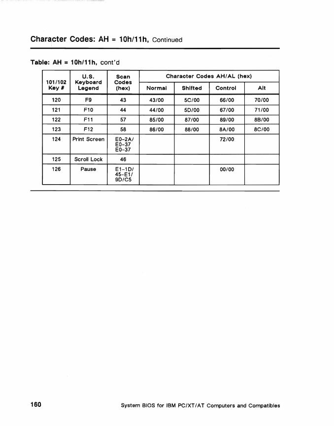
Character Codes: AH = 1Oh/11 h, Continued
Table: AH =10h/11h, cont'd
u.s. 101/102 Keyboard Key # Legend
120 F9
121 F10
122 F11
123 F12
124 Print Screen
125 Scroll Lock
126 Pause
Scan Codes (hex)
43
44
57
58
EO-2AI EO-37 EO-37
46
E1-101 4S-E11 90/C5
Character Codes AH/AL (hex)
Normal Shifted Control Alt
43100 5CI00 66/00 70100
44/00 50/00 67/00 71/00
85/00 87/00 89/00 8B/00
86/00 88/00 8A/00 8C/00
72/00
00/00
System BIOS for IBM PC/XT I AT Computers and Compatibles 160
Chapter 9
INT 10h Video Service
Overview
Description
In general, all IBM PC/XT/AT and compatible video BlOSs contain a group of functions that allow the user to select video display mode, cursor addressing, text display, scrolling, and writing pixels. However, the physical location and number of functions supported by a PC/XT/AT or compatible video BIOS depends on the kind of adapter in place.
MDA and CGA adapters rely exclusively on the Video Service contained in the system board ROM BIOS of all PC/XT/AT and compatible computers. EGA and VGA adapters contain a dedicated ROM BIOS installed on the adapter hardware itself.
How the functions are invoked
Be they in system or adapter ROM, all video BIOS functions are invoked by INT 10h. The INT 10h vector resides at interrupt table address OO:40h and is initialized to absolute address FF065h.
continued
INT 10h Video Service 161

Overview, Continued
Determining video BIOS support [MDA] [CGA] [EGA] [VGA]
Since the introduction of the IBM PC in 1981, four video adapter types have emerged: the MDA, CGA, EGA, and the VGA. The number and sophistication of the functions supported by the video BlOSs associated with each adapter varies; the more recent the adapter, the greater the number of functions its BIOS supports.
In order to identify which function is supported by which adapter, we have adopted the legend above. When a function applies exclusively to the VGA adapter, for example, its description will bear the legend [VGA]. When the function applies to all adapter types, it will bear the legend [MDA] [CGA] [EGA] [VGA].
The table below describes the meaning of each legend.
Legend Description
[MDAI Function Is supported by IBM Monochrome Display Adapters (MDA) , and compatibles.
[CGA] Function Is supported by IBM Color Graphics Adapter (CGA), and compatibles.
[EGA] Function is supported by IBM Enhanced Graphics Adapter (EGA). and compatibles.
[VGAI Function is supported by iBM Video Graphics Array (VGA) and compatible adapters.
Note: The Hercules display adapter allows for the display of 720x350 monochrome graphics on standard TTL monochrome monitors. However, neither the system ROM BIOS nor the Hercules adapter itself contain a BIOS. Applications programs that support Hercules graphics must contain an application-specific device driver.
continued
System BiOS for IBM PC/XT I A T Computers and Compatibles 162
Overview, Continued
In this chapter
This chapter defines the features and functions of all PC-compatible video and ROM BlOSs. The following topics are presented:
• Theory of Operation
• MDA Hardware Environment
• CGA Hardware Environment
• EGA Hardware Environment
• VGA Hardware Environment
• Video Modes
• System RAM Data
• Summary of INT 10h Functions
• How Functions Are Called
• Error Handling
• Video BIOS Function Descriptions
INT 10h Video Service 163
Theory of Operation
Introduction
A computer monitor is a specialized device designed to display digital data written into a video buffer by the computer's microprocessor. The signals driving the monitor originate in the computer's video subsystem. Computer monitors in themselves are not programmable, but the video subsystems controlling them are. The BIOS Video Service offers operating systems and applications programs a set of functions that eliminate the need to directly program video subsystem hardware.
How information is "painted" on the screen
The front surface on a computer monitor - the computer screen - is actually the end a large Cathode Ray Tube (CRT). The rearmost part of the CRT contains a cathode that, when heated to approximately 600 degrees Centigrade, emits a high voltage, narrowly focused, electron beam. When the electron beam strikes the phosphor coated inner surface of the computer screen, it causes an area of the phosphor to glow. When the voltage of the beam is modulated, so too is the intensity of the CRT's glow.
The computer's video subsystem generates signals that cause the CRT's electron beam to sweep across the screen in a left to right, top to bottom pattern of horizontal lines called a raster. The information written by the microprocessor to the video buffer is represented on the CRT screen as a pattern of illuminated dots, called pixels (picture elements). As the beam sweeps across the screen, the video subsystem turns the electron beam on and off, thus .. painting" the buffer information onto the screen.
continued
System BIOS for IBM PC/XT I AT Computers and Compatibles 164

Theory of Operation, Continued
Display resolution
A monitor's horizontal scan frequency determines the maximum number of lines the monitor is capable of painting per second. Its vertical scan frequency determines the frames per second the monitor is capable of refreshing .
• Vertical resolution A display's vertical resolution - the maximum number of scan lines it can display on the screen - is calculated by dividing horizontal scan frequency by vertical scan frequency.
IBM PC (and compatible) monochrome displays, for example, have a horizontal scan frequency of 18.432 KHz and a vertical scan frequency of 50Hz. The maximum number of lines displayed on the screen is calculated as follows:
18,432 KHz (lines per second) = 368 lines per frame
50 Hz (frames per second)
To allow for vertical centering of the display image, approximately 5 percent of the maximum displayable lines must be subtracted from the total. Thus maximum vertical resolution is 350 lines.
• Horizontal resolution The dots, or pixels, that appear on each horizontal scan line are generated by the video subsystem controlling the monitor. Physically, the dots are generated by a crystal-driven device, called a dot clock. A display's horizontal resolution - the maximum number of dots per line - is calculated by dividing the monitor's horizontal scan frequency into the dot rate of the subsystem driving the monitor.
The Monochrome Display Adapter, or MDA, (about which we will learn more later) has a dot clock rate of 16.257 MHz, or 16,257,000 dots per second. When driving an IBM-compatible monochrome display, maximum dots per line are calculated as follows:
16.257 MHz (16,257.000 dots per second) = 882 pixels per line
18.432 KHz (18,432 lines per second)
To allow for horizontal centering of the displayed image, 10 to 15 percent of the maximum displayable pixels must be subtracted from this total. Thus maximum horizontal resolution is 720 pixels.
continued
INT 10h Video Service 165
Theory of Operation, Continued
Monitor types
Computer monitors come in two varieties: color and monochrome.
• Colo'r monitors Color computer monitors contain three electron guns: one red, one blue, and one green. The special phosphors coating the CRT surface glow accordingly: when struck by a red beam they glow red; when struck by a blue beam, they glow blue, and so on. Although each gun illuminates a separate dot, the dots are so tightly focused that they appear to the eye as one color.
• Monochrome monitors Monochrome monitors have only one electron gun. The color of the screen is a function of the phosphor used. In monochrome computer displays, common phosphor colors are amber. green. or white.
Signal types
Computer monitors are further distinguished from each other by the kind of input signal they are designed to accept:
• Composite Composite monitors accept a composite. analog signal - like the signal used to drive a television set. In a composite color signal, the red, green, and blue (and other control signals) are combined by the video subsystem and separated by the monitor. Composite monochrome signals are the same except that they contain only one "color" signal. Composite signals can be sent over a single line, but the difficulty involved in accurately separating colors limits the resolution achieved on composite monitors.
continued
System BIOS for IBM PC/XT I A T Computers and Compatibles 166

Theory of Operation, Continued
Signal types, cont'd
• Digital RGB and digital monochrome Digital RGB monitors accept signals for red, green, or blue on separate lines. The monitor does not perform color signal separation. The number of colors displayed by a digital RGB monitor is a function of the number of color lines. A 64-color RGB monitor, such as the IBM Enhanced Color Display, is driven by two lines for each primary color. Since each pair of lines can combine into four possible intensities, 64 colors are possible (Le., 4 x 4 x 4 = 64). A digital monochrome signal is identical to its RGB counterpart except that only one "color" line is required .
• Analog RGB and monochrome Analog RGB monitors accept signals for red, green, and blue on separate lines. The number of colors potentially displayable, however, is infinite, since the intensity of each line varies with the voltage applied to it. Video subsystems designed to drive analog color monitors must convert digital color information into analog voltages.
The practical limit on the number of displayable colors is determined by the number of digital bits dedicated to each color line. A video subsystem that devotes 6 bits per color would be capable of generating signals for 262,144 different colors (Le. 2 (3*6) = 262,144). Monochrome analog signals are identical to color analog signals save that they transmit only one "color" signal. A video subsystem that devotes six bits per "color" would be capable of generating 64 shades of that color (Le., 26 = 64).
continued
INT 10h Video Service 167

Theory of Operation, Continued
Adapter types
IBM PC/XTs, ATs, and compatible systems are not manufactured with the video subsystem integrated in the motherboard; video hardware, instead, must be configured into the system bus on a video adapter board.
The table below describes monitors and resolutions supported by the major PC video adapters.
Adapter Year Dot Monitor Horlz. Vert. Resolution Type Intro. Clock Support Freq. Freq. Color
MDA 1981 16.257 MHz Digital Mono 18.43 KHz 50 Hz 720x350
HGC 1982 16.257MHz Digital Mono 18.43 KHz 50 Hz 720x350
CGA 1981 14.318 MHz Composite Color 15.75 KHz 60 Hz 640x200 Digital RGB'
EGA 1985 16.257 MHz 14.318 MHz 16.257 MHz
Digital RGB" Digital RGB' Digital Mono
21.85 KHz 15.75 KHz 18.43 KHz
60 Hz 60 Hz 50 Hz
640x350 640x200 720x350
VGA 1987 25.175 MHz 28.175 MHz 25.175 MHz 25.175 MHz
Analog'" Analog'" Analog'·' Analog··'
31.5 KHz 31.5 KHz 31.5 KHz 31.5 KHz
70 Hz 70 Hz 60 Hz 70 Hz
640x400 720x400 640x480 640x350
Legend: . IBM Color Display or compatible MDA = Monochrome Display Adapter ..HGC = Hercules Graphics Card IBM Enhanced Color Display or CGA = Color Graphics Adapter compatible EGA = Enhanced Graphics Adapter ••• IBM VGA Analog or compatible VGA = Video Graphics Array
continued
System BIOS for IBM PC/XT/AT Computers and Compatibles 168

Theory of Operation, Continued
Video data format
Each location in the video adapter's display buffer maps to a location on the display screen. The first byte of buffer memory maps to the top, leftmost point on the screen. As memory addresses increase, the screen location mapped moves from left to right and top to bottom. The microprocessor writes information to the video hardware's data buffer in either of two formats: alphanumeric or graphic .
• Alphanumeric format When writing alphanumeric data to the video buffer, the microprocessor writes each symbol (e.g., letter, number, punctuation mark, etc.) as a series of two bytes. The first byte contains the ASCII code for the symbol, and the second byte contains the color attributes to be applied to the symbol.
Alphanumeric characters are painted on the screen in a matrix of dots, called a character cell. The video subsystem's control circuitry reads one display line of ASCII data from the yideo buffer and converts it into the necessary series of dots. Simultaneously, the video hardware translates the ASCII character's accompanying attribute into the indicated foreground/bl;lckground colors .
• Graphic format When writing graphical data to the video buffer, the microprocessor writes the individual color value of each pixel to be. painted on the CRT. In order to do this, the microprocessor must address the display buffer as a memory map made up of a series of bits. When displaying data in any of 16 colors, for example, the microprocessor writes four bits per pixel (i.e., 24 =16). The video subsystem's control circuitry reads each pixel location from the buffer and generates the color and control signals necessary to write the dot to the correct screen location.
continued
INT 10h Video Service 169

Theory of Operation, Continued
Adapters, modes, and BlOSs
A video mode is characterized by:
• screen resolution,
• number of displayable colors, and the
• kind of data (alphanumeric or graphic) displayed.
Most PC video adapters support more than one video mode. The reason for this is largely historical: PC video adapters have evolved from low resolution, 16-color devices to relatively high resolution, 256K-color devices. In order to maintain compatibility with software written for the previous video adapters, each successive generation of video hardware had to be made modecompatible with its predecessors. Thus the video modes supported by eGA adapters (1981) are also supported by the more current VGA adapters (1987) .
Establishing a video mode is a matter of programming those components of the video adapter's hardware that control the adapter's dot clock, enable or disable the adapter hardware generation of alphanumeric dot patterns, and so on. Although it is possible to program these components directly, setting video modes is more easily accomplished through the video BIOS.
The physical location and number of functions supported by a video BIOS depends on the kind of adapter in place. MDA and CGA adapters rely exclusively on the Video Service contained in the system board ROM BIOS of all PC/XT/AT and compatible computers. EGA and VGA adapters contain a dedicated ROM BIOS installed on the adapter hardware itself.
continued
System BIOS for IBM PC/XT/AT Computers and Compatibles 170

Theory of Operation, Continued
Compatibility and portability
In addition to simplifying mode sets, the video BIOS contains a group of other functions that further insulate applications software from direct manipulation of video hardware. For example, the Video Service contains functions that allow users to write a dot on the screen, write a string of ASCII characterS to a specified screen location, to control the location of the cursor, and so on.
Application software can be made to execute faster if it writes directly to the video hardware. In fact, this is a common strategy used by the authors of games and other software. However, writing applications directly to the video hardware ties the application to the hardware, for there is never a guarantee that the next generation video adapter will be 100% hardware compatible with its predecessors. The BIOS that interfaces with each generation of hardware generally contains a superset of the functions supported by the previous version. Writing software to an adapter's video BIOS instead of directly to its hardware helps insure the application's longevity and portability.
Adapter hardware components
When viewed on the highest functional level, all PC video adapters share the same programmable components:
• Video Buffer An adapter's video buffer is a block of RAM that exists on the adapter but is mapped into the microprocessor's address space. Each location in the video buffer maps to a location on the video screen. The video buffer address map can range from segment BOOO:OOOOh - BOOO:BFFFh for MDA adapters to AOOO:OOOOh - BOOO:FFFFh for VGA adapters. (See Video Modes in this chapter.)
• Cathode Ray Tube Controller (CRTC) The CRTC generates the horizontal and vertical timing signals that control the path and duration of the electron beam sweeping the inner surface of the CRT. The CRTC also increments a video buffer address counter so that the data contained in the buffer will be synchronized with the timing signals. The CRTC controls the size/location of the text mode cursor, and selects the portion of the video buffer to be displayed on the screen.
continued
INT 10h Video Service 171
Theory of Operation, Continued
Adapter hardware components, cont'd
• Hardware Alphanumeric Character Generator In alphanumeric modes, characters are written to the video buffer as pairs of bytes. The first byte represents the character's ASCII value; the second byte represents the character's attribute (i.e. foreground/background color, blinking, intensity). The hardware character generator is responsible for translating the ASCII value of a character into a matrix of dots to display on the screen. To do this, the hardware character generator must reference a character table under the control of the video BIOS. Depending on adapter type, this character table can resides permanently at a fixed ROM location, or it can be written (on mode set) from ROM to a fixed location in RAM.
• Attribute Decoder An adapter's attribute decoder component uses data from the video buffer to control the color and brightness of the signals produced by the video Signal generator.
• Video Signal Generator An adapter's video signal generator component outputs the signals that control what appears on the monitor's screen. As we have seen there are three kinds of signals: composite, digital, and analog.
• Mode Control Registers Video mode control registers put the video adapter hardware in a state that will allow it to produce the indicated mode. For example, in graphics modes, the character generator must be disabled. The adapter's character clock, which determines the number of dots that are put up for each ASCII character in alphanumeric modes can vary from mode to mode. Characters can be 9 dots wide in some modes and 8 dots wide in others.
continued
System BIOS for IBM PC/XTIAT Computers and Compatibles 172

Theory of Operation, Continued
Putting a character on the screen
Video BIOS Function AH = 09h is used to write a character and its attribute to the screen. This illustratio'n shows how the video BIOS and video adapter hardware interact when Function AH = 09h is called.
ASCII Attribute ... Video BIOS 43h 07h
43h 07h Attribute I I ~ DecoderI I I I I I I I I I
L _____ 07hI t-- AlphanumericL ______
Character43h ~ Generator
Operating System or
Application Software
Call INT 10h AH = 09h
Dot Stream to Monitor
..-----. Microprocessor
Color Intensity
Video Signal
Generator
Dot Pattern
BufferT Horizontal & Vertical Timing jVideo AddressIBuffer
CRT Controller Mode Control
INT 10h Video Service 173

MDA Hardware Environment
Introduction
The MDA BIOS resides in system ROM and not on the MDA adapter card. The MDA BIOS assumes the following hardware environment:
• Motorola 6845 (or compatible) CRTC
• Monochrome digital signal monitor
• 4K of video RAM
Motorola 6845 CRTC and the MDA
When implemented on a MDA adapter, the Motorola 6845 CRTe contains 20 programmable, 8-bit internal registers. Nineteen of these registers control horizontal and vertical timings. The remaining register, the mode control register, is used in setting the MDA video mode.
continued
System BIOS for IBM PC/XT I AT Computers and Compatibles 174
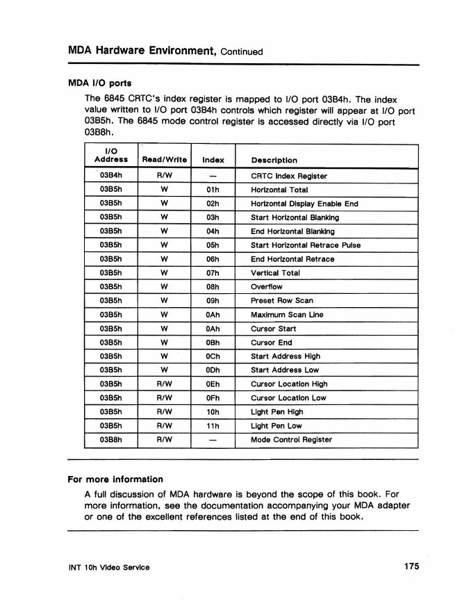
MDA Hardware Environment, Continued
MDA 1/0 ports
The 6845 CRTC's index register is mapped to I/O port 03B4h. The index value written to I/O port 03B4h controls which register will appear at I/O port 03B5h. The 6845 mode control register is accessed directly via 1/0 port 03B8h.
I/O Address Read/Write Index Description
03B4h R/W - CRTC Index Register
03B5h W 01h Horizontal Total
03B5h W 02h Horizontal Display Enable End
03B5h W 03h Start Horizontal Blanking
03B5h W 04h End Horizontal Blanking
03B5h W 05h Start Horizontal Retrace Pulse
03B5h W 06h End Horizontal Retrace
03B5h W 07h Vertical Total
03B5h W 08h Overflow
03B5h W 09h Preset Row Scan
03B5h W OAh Maximum Scan Line
03B5h W OAh Cursor Start
03B5h W OBh Cursor End
03B5h W OCh Start Address High
03B5h W OOh Start Address Low
03B5h R/W OEh Cursor Location High
03B5h R/W OFh Cursor Location Low
03B5h R/W 10h Light Pen High
03B5h R/W 11h Light Pen Low
03B8h R/W - Mode Control Register
For more information
A full discussion of MDA hardware is beyond the scope of this book. For more information. see the documentation accompanying your MDA adapter or one of the excellent references listed at the end of this book.
INT 10h Video Service 175

eGA Hardware Environment
Introduction
The CGA BIOS resides in system ROM and not on the CGA adapter card. The CGA BIOS assumes the following hardware environment:
• Motorola 6845 (or compatible) CRTC
• Composite or Digital RGB monitor
• 16K of video RAM
Motorola 6845 CRTC and the CGA
When implemented on a CGA adapter, the Motorola 6845 CRTC contains 21 programmable, 8-bit internal registers. Nineteen of these registers control horizontal and vertical timings. The remaining two registers, the mode control and palette registers, are used to set video modes and program the CGA palette.
continued
System BIOS for IBM PC/XTIA T Computers and Compatibles 176

eGA Hardware Environment, Continued
eGA 1/0 ports
The 6845 CRTC's index register is mapped to 1/0 port 03D4h. The value written to 1/0 port 03D4h controls the register that appears at port 03D5h. Mode control and palette registers are accessed via ports 03D8h and 03D9h.
I/O Address Read/Write Index Description
03D4h R/W - CRTC Index Register
03D5h W 01h Horizontal Total
03D5h W 02h Horizontal Display Enable End
03D5h W 03h Start Horizontal Blanking
03D5h W 04h End Horizontal Blanking
03D5h W 05h Start Horizontal Retrace Pulse
03D5h W 06h End Horizontal Retrace
03D5h W 07h Vertical Total
03D5h W 08h Overflow
03D5h W 09h Preset Row Scan
03D5h W OAh Maximum Scan Line
03D5h W OAh Cursor Start
03D5h W OBh Cursor End
03D5h W OCh Start Address High
03D5h W ODh Start Address Low
03D5h R/W OEh Cursor Location High
03D5h R/W OFh Cursor Location Low
03D5h R/W 10h Light Pen High
03D5h R/W 11h Light Pen Low
03D8h R/W - Mode Control Register
03D9h R/W - Palette Register
For more information
A full discussion of CGA hardware is beyond the scope of this book. For more information, see your CGA adapter riocumentation.
INT 10h Video Service 177

EGA Hardware Environment
Introduction
The EGA BIOS resides in EGA adapter cards, completely superseding the system ROM video BIOS. The EGA BIOS assumes the following hardware environment:
• IBM EGA or compatible chip • 64K of video RAM
• Digital RGB or digital monochrome monitor
EGA proprietary LSI chip
EGA adapters are controlled by an IBM (or compatible) LSI CRTC chip.
EGA 1/0 port addressing
The IBM EGA (or compatible) chip is a Large Scale Integration (LSI) device that incorporates the functionality of four general purpose adapter control registers, a CRTC, an Attribute Controller, an Address Sequencer, and a Graphics Controller onto one chip.
The limited I/O address space of PC/XT/AT and compatible computers, makes it impossible to assign each register its own I/O port. With the exception of the general registers, each major EGA register group is addressed via an index/access port pair. For example, the EGA Sequencer's index register is mapped to I/O port 03C4h. The value (index) written to port 03C4h determines which register appears at I/O port 03C5h.
continued
System BIOS for IBM PC/XT/AT Computers and Compatibles 178
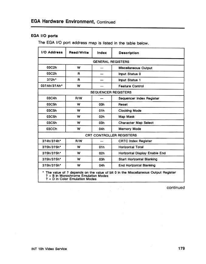
EGA Hardware Environment, Continued
EGA 1/0 ports
The EGA I/O port address map is listed in the table below.
I/O Address
03C2h
03C2h
3?2h*
03?Ah/3? Ah*
03C4h
03C5h
03C5h
03C5h
03C5h
03CCh
3?4h/3?4h*
3?5h/3?5h*
3?5h/3?5h*
3?5h/3?5h*
3?5h/3?5h*
Read/Write Index Description
GENERAL REGISTERS
W - Miscellaneous Output
R - Input Status 0
R - Input Status 1
W - Feature Control
SEQUENCER REGISTERS
R/W -W OOh
W 01h
W 02h
W 03h
W 04h
Sequencer index Register
Reset
Clocking Mode
Map Mask
Character Map Select
Memory Mode
CRT CONTROLLER REGISTERS
R/W
W
W
W
W
-01h
02h
03h
04h
CRTC Index Register
Horizontal Total
Horizontal Display Enable End
Start Horizontal Blanking
End Horizontal Blanking
* The value of ? depends on the value of bit 0 In the Miscellaneous Output Register ? = B In Monochrome Emulation Modes ? = D In Color Emulation Modes
continued
INT 10h Video Service 179
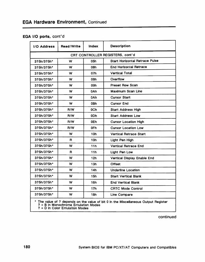
EGA Hardware Environment, Continued
EGA 1/0 ports. cont'd
1/0 Address Read/Wrlte Index Description
CRT CONTROLLER REGISTERS, cont'd
3?5h/3?5h* W 05h Start Horizontal Retrace Pulse
3?5h/3?5h* W 06h End Horlzor,tal Retrace
3?5h/3?5h* W 07h Vertical Total
3?5h/3?5h* W 08h Overflow
3?5h/3?5h* W 09h Preset Row Scan
3?5h/3?5h* W OAh Maximum Scan Line
3?5h/3?5h* W OAh Cursor Start
3?5h/3?5h* W OBh Cursor End
3?5h/3?5h* R/W OCh Start Address High
3?5h/3?5h* R/W ODh Start Address Low
3?5h/3?5h* R/W OEh Cursor Location High
3?5h/3?5h* R/W OFh Cursor Location Low
3?5h/3?5h* W 10h Vertical Retrace Start
3?5h/3?5h* R 10h Light Pen High
3?5h/3?5h* W 11h Vertical Retrace End
3?5h/3?5h* R 11h Light Pen Low
3?5h/3?5h* W 12h Vertical Display Enable End
3?5h/3?5h* W 13h Offset
3?5h/3?5h* W 14h Underline Location
3?5h/3?5h* W 15h Start Vertical Blank
3?5h/3?5h* W 16h End Vertical Blank
3?5h/3?5h* W 17h CRTC Mode Control
3?5h/3?5h* W 18h Line Compare
* The value of ? depends on the value of bit 0 in the Miscellaneous Output Register ? = B In Monochrome Emulation Modes ? = 0 in Color Emulation Modes
continued
System BIOS for IBM PC/XT I AT Computers and Compatibles 180

EGA Hardware Environment, Continued
EGA 1/0 ports, cont'd
I/O Address Read/Write Index Description
A TTRIBUTE CONTROLLER REGISTERS
03COh W -03COh W OOh-OFh
03COh W 10h
03COh W 11 h
03COh W 12h
03COh W 13h
Attribute Controller Index Register
Palette Registers OOh - OFh
Attribute Mode Control Register
Overscan Color Register
Color Plane Enable Register
Horizontal PEL Panning Register
GRAPHICS CONTROLLER REGISTERS
03CAh R/W -03CCh R/W -03CEh R/W -
03CFh R/W OOh
03CFh R/W 01h
03CFh R/W 02h
03CFh R/W 03h
03CFh R/W 04h
03CFh R/W OSh
03CFh R/W 06h
03CFh R/W 07h
03CFh R/W OSh
For more information
Graphics 2 Position Register
Graphics 1 Position Register
Graphics Controller Index Register
Set/Reset
Enable Set/Reset
Color Compare
Data Rotate
Read Map Select
Graphics Mode Register
Miscellaneous
Color Don't Care
Bit Mask
A full discussion of EGA hardware is beyond the scope of this book. For more information, see the documentation accompanying your EGA adapter or one of the excellent references listed at the end of this book.
INT 10h Video Service 181
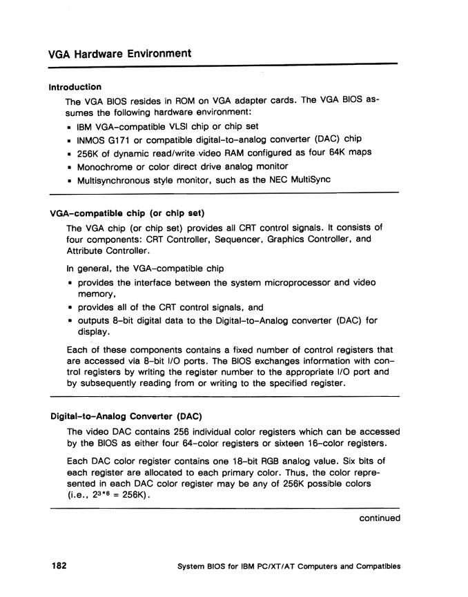
VGA Hardware Environment
Introduction
The VGA BIOS resides in ROM on VGA adapter cards. The VGA BIOS assumes the following hardware environment:
• IBM VGA-compatible VLSI chip or chip set
• INMOS G171 or compatible digital-to-analog converter (DAC) chip
• 256K of dynamic read/write .video RAM configured as four 64K maps
• Monochrome or color direct drive analog monitor
• Multisynchronous style monitor, such as the NEC MultiSync
VGA-compatible chip (or chip set)
The VGA chip (or chip set) provides all CRT control signals. It consists of four components: CRT Controller, Sequencer, Graphics Controller, and Attribute Controller.
In general, the VGA-compatible chip
• provides the interface between the system microprocessor and video memory,
• provides all of the CRT control signals, and
• outputs 8-bit digital data to the Digital-to-Analog converter (DAC) for display.
Each of these components contains a fixed number of control registers that are accessed via 8-bit I/O ports. The BIOS exchanges information with control registers by writing the register number to the appropriate I/O port and by subsequently reading from or writing to the specified register.
Digital-to-Analog Converter (DAC)
The video DAC contains 256 individual color registers which can be accessed by the BIOS as either four 64-color registers or sixteen 16-color registers.
Each DAC color register contains one 18-bit RGB analog value. Six bits of each register are allocated to each primary color. Thus, the color represented in each DAC color register may be any of 256K possible colors (i.e., 23 *6 = 256K).
continued
System BIOS for IBM PC/XT I A T Computers and Compatibles 182
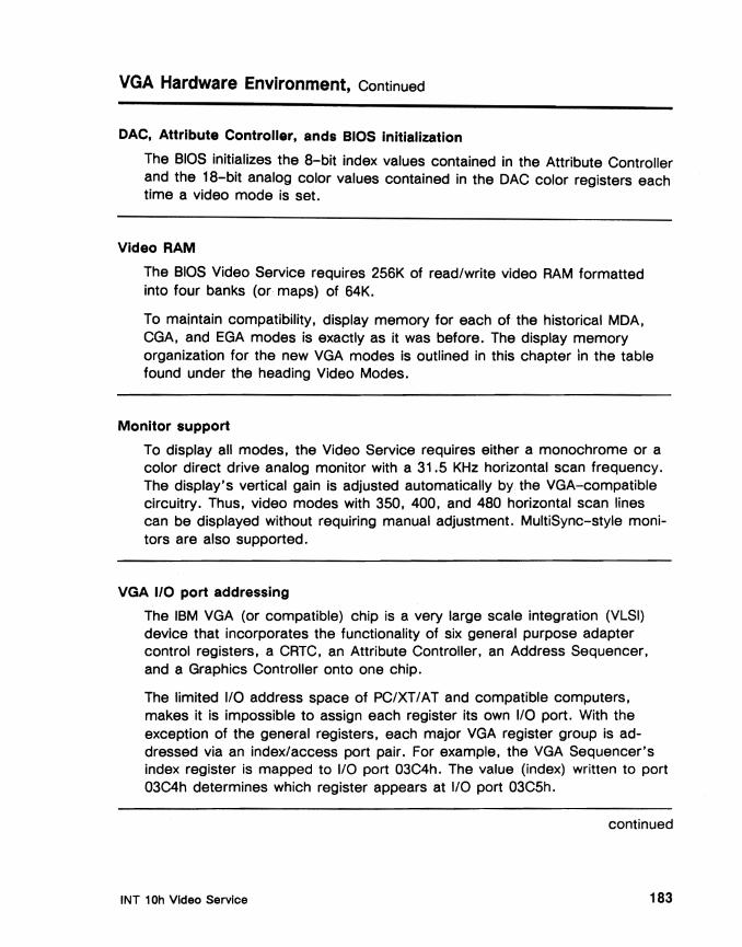
VGA Hardware Environment, Continued
DAC, Attribute Controller, ands BIOS initialization
The BIOS initializes the 8-bit index values contained in the Attribute Controller and the 18-bit analog color values contained in the DAC color registers each time a video mode is set.
Video RAM
The BIOS Video Service requires 256K of read/write video RAM formatted into four banks (or maps) of 64K.
To maintain compatibility, display memory for each of the historical MDA, CGA, and EGA modes is exactly as it was before. The display memory organization for the new VGA modes is outlined in this chapter in the table found under the heading Video Modes.
Monitor support
To display all modes, the Video Service requires either a monochrome or a color direct drive analog monitor with a 31.5 KHz horizontal scan frequency. The display's vertical gain is adjusted automatically by the VGA-compatible circuitry. Thus, video modes with 350, 400, and 480 horizontal scan lines can be displayed without requiring manual adjustment. MultiSync-style monitors are also supported.
VGA 110 port addressing
The IBM VGA (or compatible) chip is a very large scale integration (VLSI) device that incorporates the functionality of six general purpose adapter control registers, a CRTC, an Attribute Controller, an Address Sequencer, and a Graphics Controller onto one chip.
The limited I/O address space of PC/XT/AT and compatible computers, makes it is impossible to assign each register its own I/O port. With the exception of the general registers, each major VGA register group is addressed via an index/access port pair. For example, the VGA Sequencer's index register is mapped to 1/0 port 03C4h. The value (index) written to port 03C4h determines which register appears at I/O port 03C5h.
continued
INT 10h Video Service 183
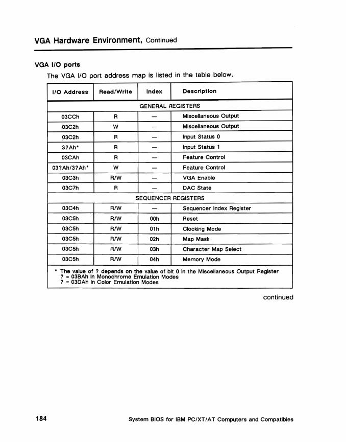
VGA Hardware Environment, Continued
VGA 110 ports
The VGA I/O port address map is listed in the table below.
110 Address Read/Write Index Description
03CCh R
03C2h W
03C2h R
3?Ah* R
03CAh R
03?Ah/3?Ah* W
03C3h R/W
03C7h R
GENERAL REGISTERS
- Miscellaneous Output
- Miscellaneous Output
- Input Status 0
- Input Status 1
- Feature Control
- Feature Control
- VGA Enable
- DAC State
SEQUENCER REGISTERS
03C4h R/W 03C5h R/W OOh
03C5h R/W 01h
03C5h R/W 02h
03C5h R/W 03h
03C5h R/W 04h
Sequencer Index Register
Reset
Clocking Mode
Map Mask
Character Map Select
Memory Mode
* The value of ? depends on the value of bit 0 In the Miscellaneous Output Register ? = 03BAh In Monochrome Emulation Modes ? = 03DAh In Color Emulation Modes
continued
System BIOS for IBM PC/XT/AT Computers and Compatibles 184
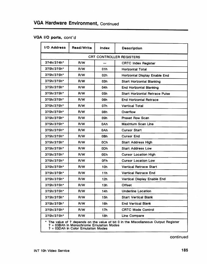
VGA Hardware Environment, Continued
VGA 1/0 ports, cont'd
I/O Address Read/Write Index Description
CRT CONTROLLER REGISTERS
3?4h/3?4h* R/W - CRTC Index Register
3?5h/3?5h* R/W 01h Horizontal Total
3?Sh/3?5h* R/W 02h Horizontal Display Enable End
3?5h/3?5h* R/W 03h Start Horizontal Blanking
3?5h/3?5h* R/W 04h End Horizontal Blanking
3?5h/3?5h* R/W 05h Start Horizontal Retrace Pulse
3?5h/3?5h* R/W 06h End Horizontal Retrace
3?5h/3?5h* R/W 07h Vertical Total
3?5h/3?5h* R/W OSh Overflow
3?5h/3?5h* R/W 09h Preset Row Scan
3?5h/3?5h* R/W OAh Maximum Scan Line
3?5h/3?5h* R/W OAh Cursor Start
3?5h/3?5h* R/W OBh Cursor End
3?5h/3?5h* R/W OCh Start Address High
3?5h/3?5h* R/W ODh Start Address Low
3?5h/3?5h* R/W OEh Cursor Location High
3?5h/3?5h* R/W OFh Cursor Location Low .-
3?5h/3?5h* R/W 10h Vertical Retrace Start
3?5h/3?5h* R/W 11h Vertical Retrace End
3?5h/3?5h* R/W 12h Vertical Display Enable End
3?5h/3?5h* R/W 13h Offset
3?5h/3?5h* R/W 14h Underline Location
3?5h/3?5h* R/W 15h Start Vertical Blank
3?5h/3?5h* R/W 16h End Vertical Blank
3?5h/3?5h* R/W 17h CRTC Mode Control
3?5h/3?5h* R/W 18h Line Compare
* The value of ? depends on the value of bit 0 In the Miscellaneous Output Register ? =03BAh in Monochrome Emulation Modes ? =03DAh in Color Emulation Modes
continued
INT 10h Video Service 185
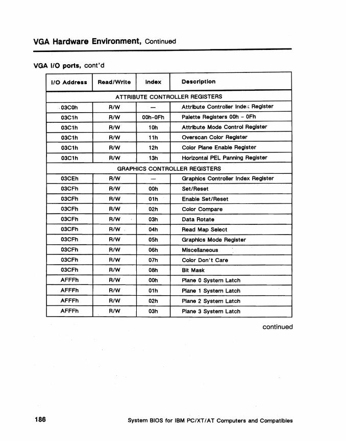
VGA Hardware Environment, Continued
VGA 1/0 ports, cont'd
I/O Address Read/Write Index Description
ATTRIBUTE CONTROLLER REGISTERS
03COh R/W - Attribute Controller Indei, Register
03C1h R/W OOh-OFh Palette Registers OOh - OFh
03C1h R/W 10h Attribute Mode Control Register
03C1h R/W 11h Overscan Color Register
03C1h R/W 12h Color Plane Enable Register
03C1h R/W 13h Horizontal PEL Panning Register
GRAPHiCS CONTROLLER REGISTERS
03CEh R/W -03CFh R/W OOh
03CFh R/W 01h
03CFh R/W 02h
03CFh R/W 03h
03CFh R/W 04h
03CFh R/W OSh
03CFh R/W 06h
03CFh R/W 07h
03CFh R/W 08h
AFFFh R/W OOh
AFFFh R/W 01h
AFFFh R/W 02h
AFFFh R/W 03h
Graphics Controller Index Register
Set/Reset
Enable Set/Reset
Color Compare
Data Rotate
Read Map Select
Graphics Mode Register
Miscellaneous
Color Don't Care
Bit Mask
Plane 0 System Latch
Plane 1 System Latch
Plane 2 System Latch
Plane 3 System Latch
continued
System BIOS for IBM PC/XT/AT Computers and Compatibles 186
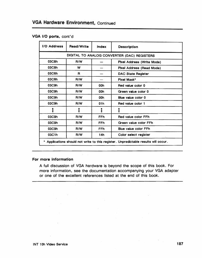
• • • • • • • • • • • •
VGA Hardware Environment, Continued
VGA 1/0 ports, cont'd
I/O Address Read/Write Index Description
DIGITAL TO ANALOG CONVERTER (DAC) REGISTERS
03C8h R/W - Pixel Address (Write Mode)
03C8h W - Pixel Address (Read Mode)
03C6h R - DAC State Register
03C6h R/W - Pixel Mask"
03C9h R/W OOh Red value color 0
03C9h R/W OOh Green value color 0
03C9h R/W OOh Blue value color 0
03C9h R/W 01h Red value color 1
03C9h R/W FFh Red value color FFh
03C9h R/W FFh Green value color FFh
03C9h R/W FFh Blue value color FFh
03C1h R/W 14h Color select register
• Applications should not write to this register. Unpredictable results will occur.
For more information
A full discussion of VGA hardware is beyond the scope of this book. For more information. see the documentation accompanying your VGA adapter or one of the excellent references listed at the end of this book.
INT 10h Video Service 181

Video Modes
MDA video mode
MDA adapters support only one video mode.
Max. Char. Max. Buff. Mode Type Resolution Colors Scheme Box P~ges Start
7 Text 720x350 mono 8Ox25 9x14 8 BOOOOh
CGA video modes
The table below lists the seven video modes supported by the CGA BIOS.
Max. Char. Max. Buff. Mode Type Resolution Colors Scheme Box Pages Start
0 Text 320x200 16 40x~5 8x8 8 B8000h
1 Text 320x200 16 40x25 8x8 8 B8000h
2 Text 640x200 16 8Ox25 8x8 8 B8000h
3 Text 640x200 16 8px25 8x8 8 B8000h
4 Graphics 320x20Q 4 40x25 8x8 1 B8000h
5 Graphics 320x200 4 40x25 8x8 1 B8000h
6 Graphics 640x200 2 8Ox25 8x8 1 B8000h
CGA video mode facts
The following facts apply to the CGA supported modes:
• No cursor is displayed in graphics modes
• Modes 1, 3, and 4 are the same as modes 0, 2,and 5 except that in modes 0, 2, and 5 color burst is enabled. Enabling color burst allows color information to be displayed on composite color displays.
• Digital RGB displays are not affected by enabling color burst.
continued
System BIOS for IBM PC/XT I AT Computers and Compatibles 188
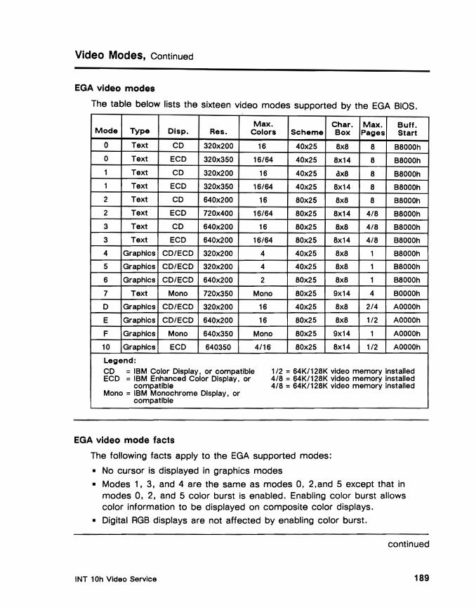
Video Modes, Continued
EGA video modes
The table below lists the sixteen video modes supported by the EGA BIOS.
Max. Char. Max. Buff. Mode Type Dlsp. Res. Colors Scheme Box Pages Start
0 Text CD 320x200 16 40x25 8x8 8 B8000h
0 Text ECD 320x350 16/64 40x25 8x14 8 B8000h
1 Text CD 320x200 16 40x25 ax8 8 B8000h
1 Text ECD 320x350 16/64 40x25 8x14 8 B8000h
2 Text CD 640x200 16 80x25 8x8 8 B8000h
2 Text ECD 720x400 16/64 80x25 8x14 4/8 B8000h
3 Text CD 640x200 16 80x25 8x8 4/8 B8000h
3 Text ECD 640x200 16/64 80x25 8x14 4/8 B8000h
4 Graphics CD/ECD 320x200 4 40x25 8x8 1 B8000h
5 Graphics CD/ECD 320x200 4 40x25 8x8 1 B8000h
6 Graphics CD/ECD 640x200 2 80x25 8x8 1 B8000h
7 Text Mono 720x350 Mono 80x25 9x14 4 BOOOOh
D Graphics CD/ECD 320x200 16 40x25 8x8 2/4 AOOOOh
E Graphics CD/ECD 640x200 16 80x25 8x8 1/2 AOOOOh
F Graphics Mono 640x350 Mono 80x25 9x14 1 AOOOOh
10 Graphics ECD 640350 4/16 80x25 8x14 1/2 AOOOOh
Legend: CD = IBM Color Display, or compatible 112 =64K/128K video memory Installed ECD =IBM Enhanced Color Display, or 4/8 =64K/128K video memory installed
compatible 4/8 =64K/128K video memory installed Mono = IBM Monochrome Display, or
compatible
EGA video mode facts
The following facts apply to the EGA supported modes:
• No cursor is displayed in graphics modes
• Modes 1, 3, and 4 are the same as modes 0, 2, and 5 except that in modes 0, 2, and 5 color burst is enabled. Enabling color burst allows color information to be displayed on composite color displays.
• Digital RGB displays are not affected by enabling color burst.
continued
INT 10h Video Service 189
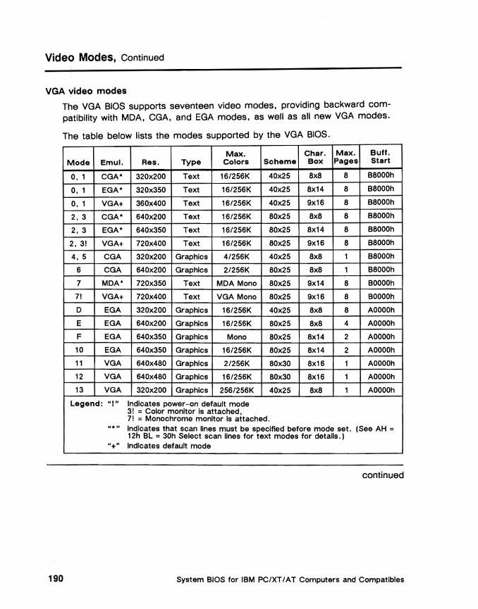
Video Modes, Continued
VGA video modes
The VGA BIOS supports seventeen video modes, providing backward compatibility with MOA, eGA, and EGA modes, as well as all new VGA modes.
The table below lists the modes supported by the VGA BIOS.
Max. Char. Max. Buff. Mode Emul. Res. Type Colors Scheme Box Pages Start
0, 1 CGA" 320x200 Text 16/256K 40x25 8x8 8 B8000h
0, 1 EGA" 320x350 Text 16/256K 40x25 8x14 8 B8000h
0, 1 VGA+ 360x400 Text 16/256K 40x25 9x16 8 B8000h
2, 3 CGA" 640x200 Text 16/256K 80x25 8x8 8 B8000h
2, 3 EGA" 640x350 Text 16/256K 80x25 8x14 8 B8000h
2, 3! VGA+ 720x400 Text 16/256K 80x25 9x16 8 B8000h
4, 5 CGA 320x200 Graphics 4/256K 40x25 8x8 1 B8000h
6 CGA 640x200 Graphics 2/256K 80x25 8x8 1 B8000h
7 MDA" 720x350 Text MDA Mono 80x25 9x14 8 BOOOOh
7! VGA+ 720x400 Text VGA·Mono 80x25 9x16 8 BOOOOh
D EGA 320x200 Graphics 16/256K 40x25 8x8 8 AOOOOh
E EGA 640x200 Graphics 16/256K 80x25 8x8 4 AOOOOh
F EGA 640x350 Graphics Mono 80x25 8x14 2 AOOOOh
10 EGA 640x350 Graphics 16/256K 80x25 8x14 2 AOOOOh
11 VGA 640x480 Graphics 2/256K 80x30 8x16 1 AOOOOh
12 VGA 640x480 Graphics 16/256K 80x30 8x16 1 AOOOOh
13 VGA 320x200 Graphics 256/256K 40x25 8x8 1 AOOOOh
Legend: "I" Indicates power-on default mode 3! =Color monitor is attached, 7! = Monochrome monitor Is attached.
"* " In~icates that scan lines must be specified before mode set. (See AH = 12h BL =30h Select scan lines for text modes for details.)
"+" Indicates default mode
continued
System BIOS for IBM PC/XT/AT Computers and Compatibles 190

Video Modes, Continued
VGA video mode facts
The facts below apply to modes listed on the previous page.
Fact Description
Modes 0, 2, 4 =modes 1, 3, 5 In eGA, modes 1, 3, and 5 have color burst turned on and modes 0, 2, and 4 have color burst turned off. The VGA hardware does not support color burst; modes 0, 2, and 4 are Identical to modes 1, 3, and 5 respectively.
200-lIne modes, double-scanned All 200 scan line modes are double-scanned by the analog monitor. Each line of video Is painted on the screen twice, one beneath the other, before the next new scan line Is painted.
No cursor in graphics The cursor Is not displayed In graphics modes.
MDA, CGA, EGA Emulation To Insure compatibility with older software, the BIOS Video Service supports all 200 and 350 scan line MDA, CGA, and EGA video modes. To activate a 200 or 350 scan line mode: . Execute Function AH =12h, BL =30h Select scan
lines for text mode with AL =OOh or 01h. (i.e., 200 or 350 scan lines).
• Execute Function AH =OOh Set Video Mode .
Note: Unless otherwise Indicated, the BIOS defaults to 400 scan lines for all text modes.
INT 10h Video Service 191

System RAM Data
Video Service data definitions
The data definitions used by thelNT 10h Video Service are stored in system RAM in segment 40h and are presented below in offset order.
System RAM Offset (hex) Size Description
49h 1 Byte Video mode setting.
4Ah 1 Word Number of columns on screen.
4Ch 1, Word Current page size.
4Eh 1 Word Current page address.
SOh 8 Words Cursor position on each page. Two bytes/page. First byte (low order) of each pair is column, second is row. 0, 0 Is upper left corner of screen.
60h 1 Word Cursor type defined as 6845 video chip-compatlbie starting and ending scan lines, High order byte holds starting scan line; low order byte holds ending scan line.
62h 1 Byte Current page number.
63h 1 Word 6845 video chip-compatible I/O port number for current mode. (Port 0304h or 03B4h)
65h 1 Byte Current mode select register.
66h 1 Byte Current palette value.
84h 1 Byte Number of rows on screen (24/25)
85h 1 Word Character height (bytes/character)
87h 1 Byte Video control bits, where: Bit 7 =Clear RAM Bit 6,5 =Memory on video hardware as follows:
OOb =64K 01b =128K 10b = 192K 11b =256K
Bit 4 =Not used Bit 3 =0 EGA-compatible mode active Bit 2 =1 Walt for display enable Bit 1 =0 Color or ECO monitor attached to
EGA-compatible adapter =1 Monochrome monitor is attached to
EGA-compatible adapter Bit 0 =0 Translate cursor video modes 0-3
when using ECO monitor In 350-line mode
continued
System BIOS for IBM PC/XT/AT Computers and Compatibles 192
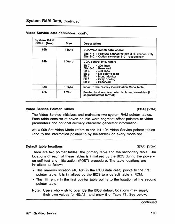
System RAM Data, Continued
Video Service data definitions, cont'd
System RAM Offset (hex) Size Description
BBh 1 Byte EGAIVGA switch data where: Bits 7-4 =Feature connector bits 3-0, respectively Bits 3-0 = Option switches 3-0, respectively
B9h 1 Word VGA control bits. where: Bit 7 =200 lines Bits 6-5 =Reserved Bit 4 =400 lines Bit 3 =No palette load Bit 2 =Mono Monitor Bit 1 =Gray Scaling Bit 0 =Reserved
BAh 1 Byte Index to the Display Combination Code table
ABh 1 Word Pointer to video parameter table and overrides (in segment:offset format).
Video Service Pointer Tables [EGA] [VGA]
The Video Service initializes and maintains two system RAM pointer tables. Each table consists of seven double-word segment:offset pointers to video parameters and optional auxiliary character generator information.
AH = OOh Set Video Mode refers to the INT 10h Video Service pointer tables (and to the information pointed to by the tables) on every mode set.
Default table locations [EGA] [VGA)
There are two pointer tables: the primary table and the secondary table. The locations of each of these tables is initialized by the BIOS during the poweron self test and initialization (POST) procedure. The table locations are initialized as follows:
• This memory location (40:A8h in the BIOS data area) points to the first pointer table. It is initialized by the BIOS to a default table in ROM.
• The fifth entry in the first pointer table points to the location of the second pOinter table.
Note: Users who wish to override the BIOS default locations may supply their own values for 40:A8h and entry 5 of Table #1. See below.
continued
INT 10h Video Service 193

System RAM Data, Continued
Structure of Video Service Pointer Table #1 [EGA] [VGA]
The location of the first, or primary, pointer table must be stored in 40:A8h. This address is initialized by the BIOS to a default location.
The table is structured as follows:
Table Location Description
Pointer 1 POINTER TO VIDEO PARAMETER TABLE Initialized at POST to the ROM BIOS video parameter table. This table entry is mandatory. If relnltlalized, It must point to a valid video parameter table.
Pointer 2 POINTER TO DYNAMIC SAVE AREA Optionai table entry. Initialized at POST to OO:OOh. When nonzero, this entry must pOint to a Dynamic Save Area In system RAM. The Dynamic Save Area must be at least 256 bytes long. It contains the 16 EGA palette register values as well as the overscan register value In bytes 0-16, respectively.
Pointer 3 POINTER TO TEXT MODE AUXILIARY CHARACTER GENERATOR Optional table entry. Initialized by the BIOS to OO:OOh. When nonzero, this entry must pOint to a table structured as below:
Size Description
Byte Bytes per character
Byte Block to load, 0 =Normal operation
Word Count to store, 256 =Normal operation
Word Character offset, 0 =Normal operation
Dword Pointer to a font table
Byte Displayable rows, where: OFFh = Maximum caiculated value otherwise
indicated number of rows displayed.
Byte Consecutive bytes of mode values for font. OFFh :: Indicates end of stream
Note: Using this third pointer can cause unexpected cursor operation. See Function AH =01h Set Text Mode Cursor Size, in this chapter for details.
continued
System BIOS for IBM PC/XT/AT Computers and Compatibles 194

System RAM Data, Continued
Structure of Video Service Pointer Table #1, cont'd [EGA] [VGA]
Table Location Description
Pointer 4 POINTER TO GRAPHICS MODE CHARACTER GENERATOR Optional table entry. Initialized to 00: OOh. When nonzero, this entry must point to a table structured as below:
Size Description
Byte Displayable rows
Word Bytes per character
DWord Pointer to font table
Byte Consecutive bytes of mode values for font. OFFh = Indicates end of stream
Pointer 5 POINTER TO VIDEO SERVICE POINTER TABLE #2 (Secondary Save Pointer Data Area) Initialized by the BIOS to the default Pointer Table #2 location. This table entry Is mandatory. If relnltlalized, it must pOint to a valid Pointer Table #2.
Pointer 6 Reserved. Set by the BIOS to OO:OOh.
Pointer 7 Reserved. Set by the BIOS to OO:OOh.
continued
INT 10h Video Service 195
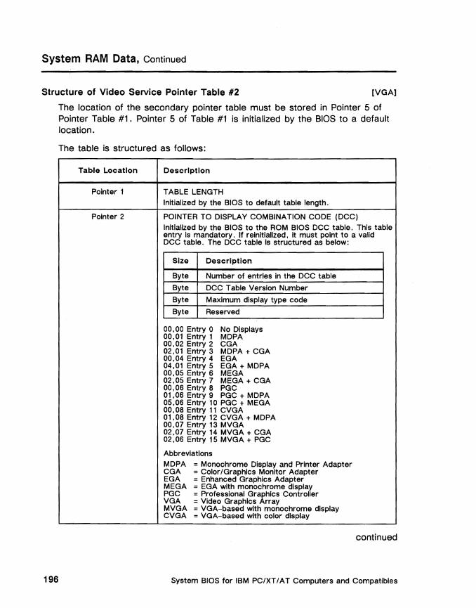
System RAM Data, Continued
Structure of Video Service Pointer Table #2 [VGA]
The location of the secondary pointer table must be stored in Pointer 5 of Pointer Table #1. Pointer 5 of Table #1 is initialized by the BIOS to a default loqation.
The table is structured as follows:
Table Location Description
Pointer 1 TABLE LENGTH Initialized by the BIOS to default table length.
Pointer 2 POINTER TO DISPLAY COMBINATION CODE (DCC) Initialized by the BIOS to the ROM BIOS DCC table. This table entry is mandatory. If relnitlalized, it must point to a valid DCC table. The DCC table Is structured as below:
Size Description
Byte Number of entries in the DCC table
Byte DCC Table Version Number
Byte Maximum display type code
Byte Reserved
00,00 Entry 0 No Displays 00,01 Entry 1 MDPA 00,02 Entry 2 CGA 02,01 Entry 3 MDPA + CGA 00,04 Entry 4 EGA 04,01 Entry 5 EGA + MDPA 00,05 Entry 6 MEGA 02,05 Entry 7 MEGA + CGA 00,06 Entry 8 PGC 01,06 Entry 9 PGC + MDPA 05,06 Entry 10 PGC + MEGA 00,08 Entry 11 CVGA 01,08 Entry 12 CVGA + MDPA 00,07 Entry 13 MVGA 02,07 Entry 14 MVGA + CGA 02,06 Entry 15 MVGA + PGC
Abbreviations MDPA =Monochrome Display and Printer Adapter CGA =Color/Graphics Monitor Adapter EGA = Enhanced Graphics Adapter MEGA = EGA with monochrome display PGC = Professional Graphics Controller VGA =Video Graphics Array MVGA =VGA-based with monochrome display CVGA =VGA-based with color display
continued
System BIOS for IBM PC/XT/AT Computers and Compatibles 196
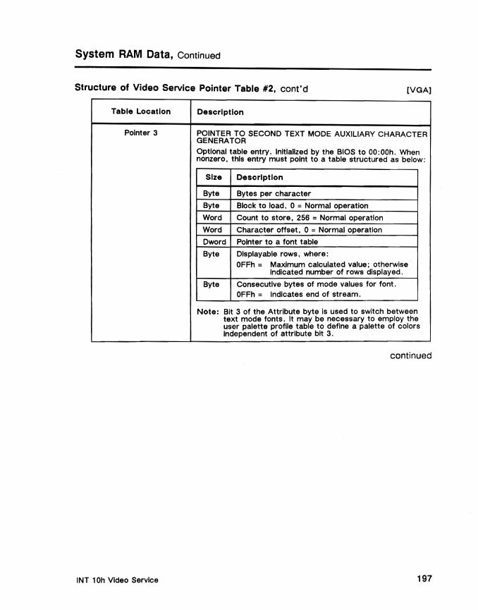
System RAM Data, Continued
Structure of Video Service Pointer Table #2, cont'd [VGA]
Table Location Description
Pointer 3 POINTER TO SECOND TEXT MODE AUXILIARY CHARACTER GENERATOR
Optional table entry. Initialized by the BIOS to 00: OOh. When nonzero, this entry must point to a table structured as below:
Size Description
Byte Bytes per character
Byte Block to load, 0 =Normal operation
Word Count to store, 256 =Normal operation
Word Character offset, 0 =Normal operation
Dword Pointer to a font table
Byte Displayable rows, where:
OFFh = Maximum calculated value; otherwise Indicated number of rows displayed.
Byte Consecutive bytes of mode values for font. OFFh = Indicates end of stream.
Note: Bit 3 of the Attribute byte is used to switch between text mode fonts. It may be necessary to employ the user palette profile table to define a palette of colors Independent of attribute bit 3.
continued
INT 10h Video Service 197

System RAM Data, Continued
[VGA]Structure of Video Service Pointer Table #2. cont'd
Table Location Description
Pointer 4 Pointer to User Palette Profile Table
Optional table entry. Initialized by the BIOS to 00: OOh. When nonzero, this entry must point to a table structured as beiow:
Size Description
Byte Underlining flag, where: 1 =On o =Ignore (Normal operation)
-1 =Off
Byte Reserved
Word Reserved
Word Internal palette count (0-17), where: 17 =Normal operation
Word internal palette index (0-16), where: o=Normal operation
DWord Pointer to Internal palette
Word External palette count (0-256), where: o=Normal operation
Word External palette Index (0-255), where: o=Normal operation
DWord Pointer to external palette
Byte Consecutive bytes of mode values for font, where: OFFh =End of stream
Pointer 5 Reserved
Pointer 7 Reserved
System BIOS for IBM PC/XTI AT Computers and Compatibles 198

Summary of INT 10h Functions [MDA] [eGA] [EGA] [VGA]
Summary of Video Service functions
The physical location and number of functions supported by a given video BIOS depends on the kind of adapter in place. MDA and eGA adapters rely exclusively on the Video Service contained in the system board ROM BIOS of all PC/XT I AT and compatible computers. EGA and VGA adapters contain a dedicated ROM BIOS installed on the adapter hardware itself.
The table below lists the Video Service functions and subfunctions. The column labeled Adapter Type defines each function's level of support for each video adapter type.
AH Description Adapter Type
OOh Set Video Mode [MDA] [CGA] [EGA] [VGA]
01h Set Text Mode Cursor Size [MDA] [CGA) [EGA) [VGA]
02h Set Cursor Position [MDA) [CGA) [EGA] [VGA]
03h Read Current Cursor Position [MDA] [CGA] [EGA) [VGA)
04h Read Light Pen Position [CGA) [EGA]
05h Select New Video Page [CGA) [EGA] [VGA)
OSh Scroll Current Page Up [MDA) [CGA] [EGA) [VGA]
07h Scroll Current Page Down [MDA) [CGA) [EGA] [VGA)
OSh Read Character/Attribute from Screen [MDA) [CGA] [EGA] [VGA)
09h Write Character/Attribute to Screen [MDA] [CGA] [EGA] [VGA]
OAh Write Character Only to Screen [MDA] [CGA) [EGA] [VGA)
OBh Set Color Palette [CGA) [EGA] [VGA)
OCh Write Pixel [CGA] [EGA] [VGA]
ODh Read Pixel [CGA) [EGA) [VGA]
OEh Write Teletype to Active Page [MDA) [CGA] [EGA] [VGA)
OFh Return Video Status [MDA] [CGA) [EGA) [VGA)
continued
INT 10h Video Service 199
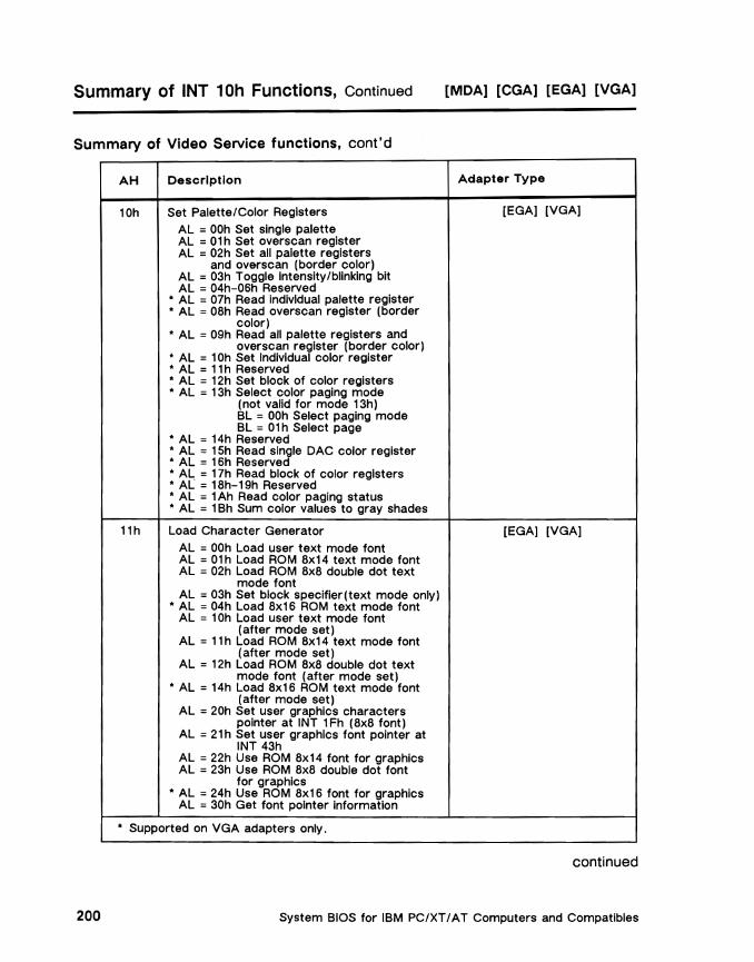
Summary of INT 10h Functions, Continued [MDA] [eGA] [EGA] [VGA]
Summary of Video Service functions, cont'd
AH Description Adapter Type
10h Set Palette/Color Registers [EGA] [VGA]
AL = OOh Set single palette AL = 01h Set overscan register AL = 02h Set all palette registers
and overscan (border color) AL = 03h Toggle Intensity/blinking bit AL = 04h-06h Reserved
• AL = 07h Read individual palette register • AL = 08h Read overscan register (border
color) • AL = 09h Read all palette registers and
overscan register (border color) • AL = 10h Set Individual color register • AL = 11 h Reserved • AL =12h Set block of color registers • AL =13h Select color paging mode
(not valid for mode 13h) BL =OOh Select paging mode BL =01 h Select page
• AL = 14h Reserved • AL = 15h Read single DAC color register • AL =16h Reserved • AL =17h Read block of color registers • AL = 18h-19h Reserved • AL = 1 Ah Read color paging status • AL =1Bh Sum color values to gray shades
11 h Load Character Generator
AL =OOh Load user text mode font AL =01h Load ROM 8x14 text mode font AL = 02h Load ROM 8x8 double dot text
mode font AL =03h Set block specifier(text mode only)
• AL =04h Load 8x16 ROM text mode font AL = 10h Load user text mode font
(after mode set) AL =11 h Load ROM 8x14 text mode font
(after mode set) AL = 12h Load ROM 8x8 double dot text
mode font (after mode set) • AL =14h Load 8x16 ROM text mode font
(after mode set) AL = 20h Set user graphics characters
pointer at INT 1 Fh (8x8 font) AL =21 h Set user graphics font pointer at
INT 43h AL = 22h Use ROM 8x14 font for graphics AL =23h Use ROM 8x8 double dot font
for graphics • AL = 24h Use ROM 8x16 font for graphics
AL = 30h Get font pointer information
• Supported on VGA adapters only.
[EGA] [VGA]
continued
System BIOS for IBM PC/XT/AT Computers and Compatibles 200

Summary of INT 10h Functions, Continued [MDA] [eGA] [EGA] [VGA]
Summary of Video Service functions. cont'd
AH Description Adapter Type
12h Alternate Select
BL =10h Return configuration Information BL =20h Switch to alternate print
screen routine • BL =30h Select scan lines for
text modes • BL =31h Enable/disable default
palette loading during set mode • BL =32h Enable/disable video • BL =33h Enable/disable summing
to gray shades • BL =34h Enable/disable cursor scaling • BL· =35h Switch display • BL =36h Video screen off/on
(EGAI (VGAI
13h Write String AL =OOh Cursor not moved AL =01h Cursor Is moved AL =02h Cursor not moved
(text modes only) AL =03h Cursor Is moved
(text modes only)
(MDAI [CGAI [EGA] [VGAI
14h-19h Reserved
1Ah Read/Write Display Combination Code [VGAI AL =OOh Read display combination code AL =01 h Write display combination code
1Bh Return Functionality/State Information [VGAI
1Ch Save/Restore Video State· AL =OOh Return Save/Restore buffer
size needed AL =01 h Save current video state AL =02h Restore current video state
[VGAI
• Supported on VGA adapters only.
INT 10h Video Service 201
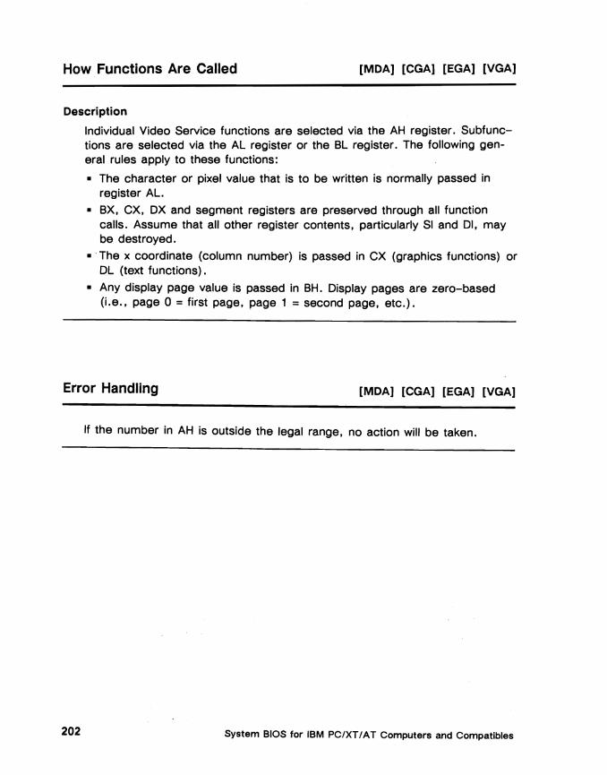
[MDA] [CGA] [EGA] [VGA]How Functions Are Called
Description
Individual Video Service functions are selected via the AH register. Subfunctions are selected via the AL register or the BL register. The following general rules apply to these functions:
• The character or pixel value that is to be written is normally passed in register AL.
• BX, ex, DX and segment registers are preserved through all function calls. Assume that all other register contents, particularly SI and DI, may be destroyed.
• . The x coordinate (column number) is passed in ex (graphics functions) or DL (text functions).
• Any display page value is passed in BH. Display pages are zero-based (i.e., page 0 = first page, page 1 = second page, etc.).
Error Handling [MDA] [CGA] [EGA] [VGA]
If the number in AH is outside the legal range, no action will be taken.
System BIOS for IBM PC/XT/AT Computers and Compatibles 202
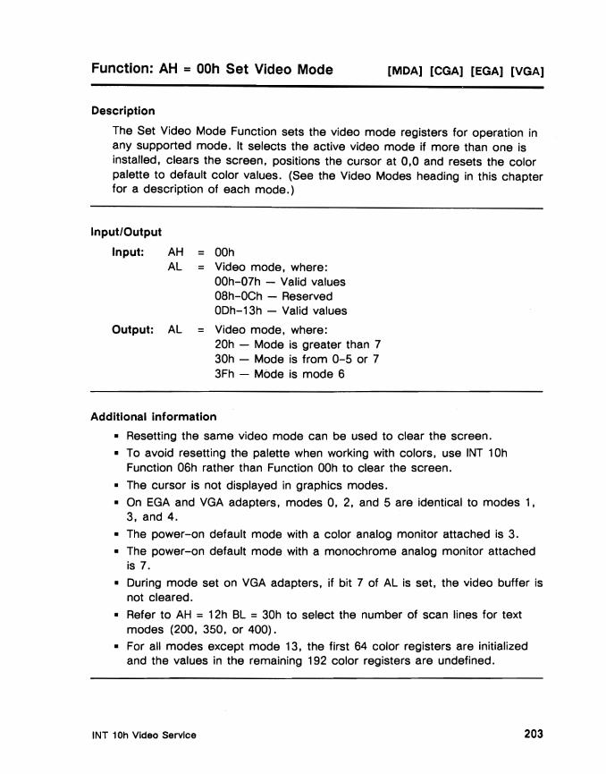
Function: AH = OOh Set Video Mode [MDA] [eGA] [EGA] [VGA]
Description
The Set Video Mode Function sets the video mode registers for operation in any supported mode. It selects the active video mode if more than one is installed, clears the screen, positions the cursor at 0,0 and resets the color palette to default color values. (See the Video Modes heading in this chapter for a description of each mode.)
Input/Output
Input: AH = OOh AL = Video mode, where:
00h-07h - Valid values OSh-OCh - Reserved ODh-13h - Valid values
Output: AL = Video mode, where: 20h - Mode is greater than 7 30h - Mode is from 0-5 or 7 3Fh - MOde is mode 6
Additional information
• Resetting the same video mode can be used to clear the screen.
• To avoid resetting the palette when working with colors, use INT 10h Function 06h rather than Function OOh to clear the screen.
• The cursor is not displayed in graphics modes.
• On EGA and VGA adapters, modes 0, 2, and 5 are identical to modes 1, 3, and 4.
• The power-on default mode with a color analog monitor attached is 3.
• The power-on default mode with a monochrome analog monitor attached is 7.
• During mode set on VGA adapters, if bit 7 of AL is set, the video buffer is not cleared.
• Refer to AH = 12h BL = 30h to select the number of scan lines for text modes (200, 350, or 400).
• For all modes except mode 13, the first 64 color registers are initialized and the values in the remaining 192 color registers are undefined.
INT 10h Video Service 203
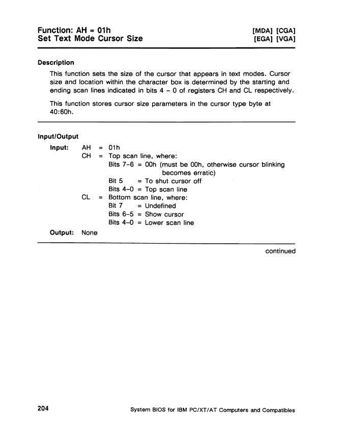
Function: AH = 01h [MDA] [eGA] Set Text Mode Cursor Size [EGA] [VGA]
Description
This function sets the size of the cursor that appears in text modes. Cursor size and location within the character box is determined by the starting and ending scan lines indicated in bits 4 - 0 of registers CH and CL respectively.
This function stores cursor size parameters in the cursor type byte at 40:60h.
Input/Output
Input: AH = 01h CH = Top scan line, where:
Bits 7-6 = OOh (must be OOh, otherwise cursor blinking becomes erratic)
Bit 5 = To shut cursor off Bits 4-0 = Top scan line
CL = Bottom scan line, where: Bit 7 = Undefined Bits 6-5 = Show cursor Bits 4-0 = Lower scan line
Output: None
continued
System BIOS for IBM PC/XT I A T Computers and Compatibles 204
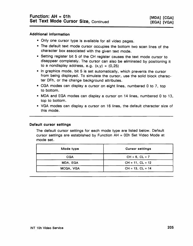
Function: AH = 01h [MDA] [eGA]Set Text Mode Cursor Size, Continued [EGA] [VGA]
Additional information
• Only one cursor type is available for all video pages.
• The default text mode cursor occupies the bottom two scan lines of the character box associated with the given text mode.
• Setting register bit 5 of the CH register causes the text mode cursor to disappear completely. The cursor can also be eliminated by positioning it to a nondisplay address, e.g. (x,y) = (0,25)
• In graphics mode, bit 5 is set automatically, which prevents the cursor from being displayed. To simulate the cursor, use the solid block character DFh, or the change background attributes.
• CGA modes can display a cursor on eight lines, numbered 0 to 7, top to bottom.
• MDA and EGA modes can display a cursor on 14 lines, numbered 0 to 13, top to bottom.
• VGA modes can display a cursor on 16 lines, the default character size of this mode.
Default cursor settings
The default cursor settings for each mode type are listed below. Default cursor settings are established by Function AH = OOh Set Video Mode at mode set.
Mode type Cursor settings
CGA CH = 6, CL = 7
MDA. EGA CH = 11, CL = 12
MCGA. VGA CH = 13, CL = 14
INT 10h Video Service 205
[MDA] [CGA] [EGA] [VGA] Function: AH = 02h Set Cursor Position
Description
The Set Cursor Position function sets the cursor position (in terms of rowby-column coordinates) for the display page indicated in BL. It saves the position as a two-byte row-by-column table entry in the cursor coordinates byte at 40:50h. Rowand column coordinates are indicated in registers DH and DL respectively.
The Set Cursor Position function applies to both text and graphics video modes. In text modes, if the display page selected in BH is the active display page, the screen cursor will move to the coordinates indicated in registers DH and DL. In graphics modes, the cursor is invisible but is used to define a position on the screen.
Input/Output
Input: AH = 02h BH Display page number (see Function AH = 05h) DH = Row (0 is top row of screen) DL = Column (0 is leftmost column)
Output: AX = OOh
Cursor Positioning
Positioning the cursor to coordinates (0,0) places it in the upper left corner of the screen in the 80x25 text mode. Selecting coordinates (79,24) in the 80x25 text mode will allow placement of the cursor in the lower right corner of the screen. The cursor can also be placed in the lower right corner of the screen using coordinates (39,24) in the 40x25 text mode.
The cursor can be turned off by moving it to an off-screen location or changing its coordinates to a position such as (0,25). However, if it is moved too far off-screen, the actual position if the cursor may become unpredictable.
Additional information
• The display page number must be set to 0 in CGA graphics mode.
• Multiple display pages in 16-color graphics as well as text modes are supported by both EGA and VGA.
System BIOS for IBM PC/XT I A T Computers and Compatibles 206
Function: AH = 03h [MDA] [eGA] Read Current Cursor Position [EGA] [VGA]
Description
The Read Current Cursor Position function reads the cursor position for the given video page from the cursor coordinates byte at 40:50h. It reads the cursor type from 40:60h and returns the current cursor position in text coordinates. This function is useful for determining the exact cursor type before it is changed.
Input/Output
Input: AH = 03h BH = Display page number (zero-based)
Output: AX = OOh CH = Starting cursor scan line CL = Ending cursor scan line DH = Row number DL = Column number
A different cursor is maintained for each display page. Each of these cursors can be examined independently with this function, no matter which page is currently active. The number of available display pages is defined by the display mode selected.
INT 10h Video Service 207
Function: AH = 04h Read Light Pen Position [eGA] [EGA]
Description
This function reads the light pen's status and position. Light pen input devices are not supported on VGA adapters. Light pens are not effective on monochrome monitors with long image-retention phosphor, and the light pen position is not accurate enough for use with high resolution devices.
Input/Output
Input: AH = 04h
Output: AH = OOh Light pen switch is not active = 01 h Light pen coordinate values
DH,DL = Rowand column of character CH = Raster line (0 -199) CL = Raster line (0 - nnn) modes> 200 line resolution BX Pixel column (0 - 319,639)
System BIOS for IBM PC/XT I A T Computers and Compatibles 208

Function: AH = OSh Select New Video Page [eGA] [EGA] [VGA]
Description
The Select New Video Page function sets the active page for the video mode selected. Refer to the table under the Video Modes heading for a list of the maximum number of pages allowed for each video mode.
Input/Output
Input: AH = OSh AL = New page number (zero-based)
Output: None
Additional information
• All page numbers are zero-based (i.e., page numbers begin at page 0).
• In text modes, page numbers range from 0-7.
• Page 0, located at the beginning of display memory, is used by default in all video modes.
• Switching between pages does not alter their contents. Also, no matter which page is active (currently displayed), text can be written to any video page using INT 10h, Functions 02h, 09h and 10h.
• In the eGA modes, no video paging is possible.
• In EGA and VGA modes, video pages are available up to the limits of video RAM in both alphanumeric and graphics modes.
• The current cursor position is maintained by the BIOS for as many as eight video pages.
• An instantaneous screen change can be created by building a screen on an undisplayed page, then using this function to display it.
INT 10h Video Service 209

Function: AH = OSh Scroll Current Page Up [MDA] [eGA] Function: AH = 07h Scroll Current Page Down [EGA] [VGA]
Description
The Scroll Current Page Up/Down functions employ the CH, DH, CL, and DL registers to define a screen window and allow the contents of the window to be scrolled either up or down by the number of character rows specified in register AL. If AL = OOh, the window is blanked instead of scrolled.
Information appearing on the screen but lying outside the parameters of the defined window remains on the screen. Only one window can be defined at any given time.
These two functions operate in both text and graphics modes.
Input/Output
Input: AH = 06h Scroll current page up 07h Scroll current page down
AL = Scroll distance in character rows (0 blanks entire scroll area)
BH = Attribute to use on blanked lines CH = Top row of scroll window CL = Left column of scroll window DH Bottom row of scroll window DL = Right column of scroll window
Output: None
Use the cursor positioning and character writing functions to fill the blank line with text.
Initializing a window
Setting AL = OOh initializes a window on the display screen. Setting the AL register to zero blanks out the region specified by the CX and DX general purpose registers and fills the window with the attribute in the BH register.
System BIOS for IBM PC/XT I AT Computers and Compatibles 210
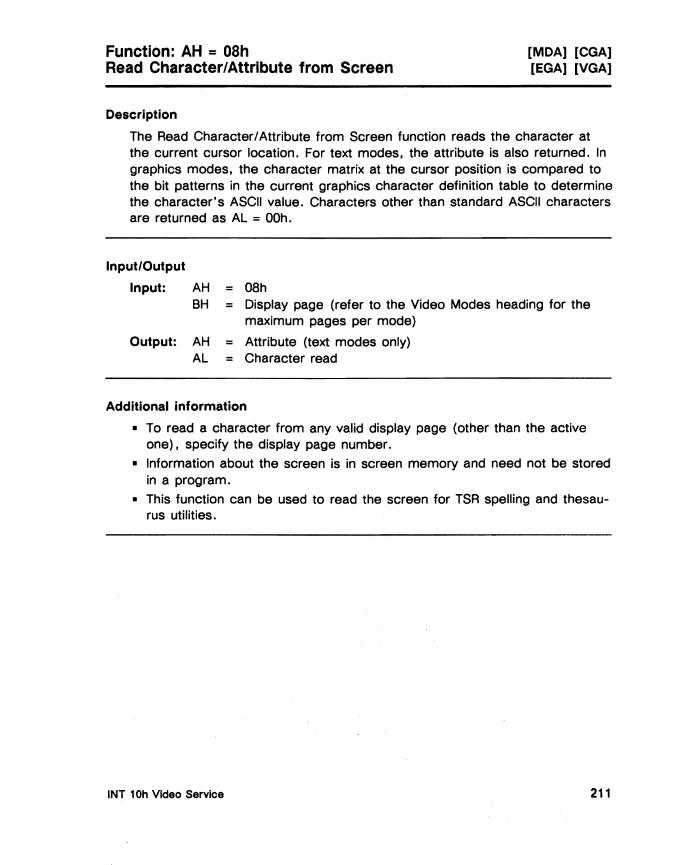
Function: AH = OSh [MDA] [eGA] Read Character/Attribute from Screen [EGA] [VGA]
Description
The Read Character/Attribute from Screen function reads the character at the current cursor location. For text modes, the attribute is also returned. In graphics modes, the character matrix at the cursor position is compared to the bit patterns in the current graphics character definition table to determine the character's ASCII value. Characters other than standard ASCII characters are returned as AL = OOh.
Input/Output
Input: AH = 08h BH = Display page (refer to the Video Modes heading for the
maximum pages per mode)
Output: AH = Attribute (text modes only) AL = Character read
Additional Information
• To read a character from any valid display page (other than the active one), specify the display page number.
• Information about the screen is in screen memory and need not be stored in a program.
• This function can be used to read the screen for TSR spelling and thesaurus utilities.
INT 10h Video Service 211

Function: AH = 09h [MDA] [eGA] Write Character/Attribute to Screen [EGA] [VGA]
Description
The Write Characterl Attribute function writes the character to the screen starting at the current cursor location for as many times as indicated in the CX register. The cursor is not moved even if more than one character is written. unless the same character is repeated.
INT 10h Functions AH = 09h and AH = OAh are similar. AH = 09h should be used for all graphics modes and in all text modes where character by character control of foreground and background attributes is desired.
Input/Output
Input: AH 09h AL = ASCII character to write BH = Display page (refer to the Video Modes heading for the
maximum pages per mode) = Background color (graphics mode 13h only)
BL = Character attribute (text modes) = Foreground color (graphics modes) (Le. color of
character) CX = Repeat count
Output: None
continued
System BIOS for IBM PC/XT I A T Computers and Compatibles 212

Function: AH = 09h [MDA] [eGA] Write Character/Attribute to Screen, Continued [EGA] [VGA]
Additional information
• In text modes, the number of repeats placed into CX may exceed the number of columns remaining in a given row. Characters will wrap around from row to row. In graphics modes, the number of repeats placed into CX cannot exceed the number of columns remaining in a given row. Characters will not wrap around from row to row.
• In VGA graphics mode 13h, the color specified in BH determines the screen background color.
• In CGA graphics modes, the bit map used for ASCII characters 80-FFh is stored in a table that starts at O:7Ch. This value is stored in the vector for INT 1 Fh. By resetting the vector, the bit map table location can be changed to point to a different bit map.
• For EGA and VGA graphics modes, use the table whose pointer is stored in the vector for INT 43h. For further information, refer to the INT 10h, Function AH = 11 h, AL = 20h and AL = 21 h headings in this chapter.
• Any value of AL will produce a display; this includes all control characters (e.g. bell, backspace, CR, LF). These control characters are not interpreted as special characters and do not change the cursor position.
• After a character has been written, the cursor has to be explicitly moved to the next position using INT 10h, Function 02h.
• To write a character without changing the attribute at the current cursor position, use INT 10h, Function OAh.
• When this function is used to write characters in graphics mode, and bit 7 of BL is set to 1, the character is XORed with the contents of the current display. This feature can be used to write characters and then erase them.
INT 10h Video Service 213
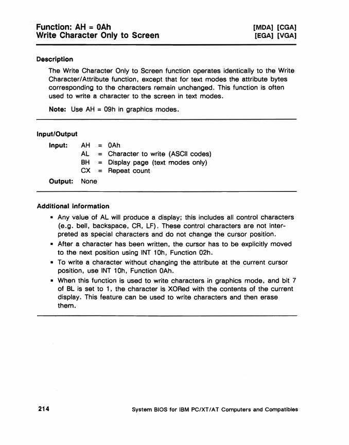
Function: AH = OAh [MDA] [eGA] Write Character Only to Screen [EGA] [VGA]
Description
The Write Character Only to Screen function operates identically to the Write CharacterIAttribute function, except that for text modes the attribute bytes corresponding to the characters remain unchanged. This function is often used to write a character to the screen in text modes.
Note: Use AH = 09h in graphics modes.
Input/Output
Input: AH = OAh AL = Character to write (ASCII codes) BH = Display page (text modes only) CX = Repeat count
Output: None
Additional Information
• Any value of AL will produce a display; this includes all control characters (e.g. bell, backspace, CR, LF). These control characters are not interpreted as special characters and do not change the cursor position.
• After a character has been written, the cursor has to be explicitly moved to the next position using INT 10h, Function 02h.
• To write a character without changing the attribute at the current cursor position, use INT 10h, Function OAh.
• When this function is used to write characters in graphics mode, and bit 7 of BL is set to 1, the character is XORed with the contents of the current display. This feature can be used to write characters and then erase them.
System BIOS for IBM PC/XT / AT Computers and Compatibles 214

Function: AH = OBh Set Color Palette [eGA] [EGA] [VGA]
Description
This function selects colors for medium resolution graphics modes. Depending on the value placed in BH, the Set Color Palette function will perform any of four operations.
If BH = OOh, then the value in BL sets the:
• background color for 320x200 graphics modes (modes 4, 5), • border color for 320x200 text modes (modes 0, 1, 2, 3),
• foreground color for 640x200 graphics mode (mode 6).
If BH = 01 h, then the value in BL sets the palette for 320x200 graphics modes (modes 4, 5).
Input/Output
Input: AH = OBh BH = OOh
= Mode = 4, 5, set background color to value in BL = Mode = 0, 1, 2, 3, set border color to value in BL = Mode = 6, set foreground color (640x200 graphics)
to value in BL BL = (0-31), when colors (16-31 are high intensity
background set)
or
BH = 01 h Select palette for modes 4, 5 (320x200 graphics) BL = OOh Palette = Green (1). Red (2), Brown (3)
= 01 h Palette = Cyan (1), Magenta (2), White (3)
Output: None
Additional information
• In CGA graphics modes, bit 4 of BL selects between normal and high intensity. EGA and VGA graphics modes emulate this by selecting a palette of high intensity colors when bit 4 of BL is set.
• A flashing display can be set by rapidly changing the palette.
• The background color of text is determined by the high order four bits of the attribute byte of each character.
INT 10h Video Service 215
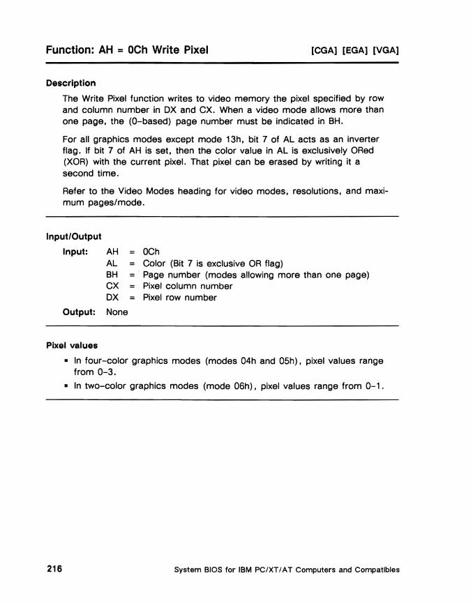
Function: AH = OCh Write Pixel [eGA] [EGA] [VGA]
Description
The Write Pixel function writes to video memory the pixel specified by row and column number in DX and CX. When a video mode allows more than one page. the (O-based) page number must be indicated in BH.
For all graphics modes except mode 13h, bit 7 of AL acts as an inverter flag. If bit 7 of AH is set, then the color value in AL is exclusively ORed (XOR) with the current pixel. That pixel can be erased by writing it a second time.
Refer to the Video Modes heading for video modes, resolutions, and maximum pages/mode.
Input/Output
Input: AH = OCh AL Color (Bit 7 is exclusive OR flag) BH = Page number (modes allowing more than one page) CX = Pixel column number DX = Pixel row number
Output: None
Pixel values
• In four-color graphics modes (modes 04h and OSh), pixel values range from 0-3.
• In two-color graphics modes (mode 06h), pixel values range from 0-1.
System BIOS for IBM PC/XT I AT Computers and Compatibles 216

Function: AH = ODh Read Pixel [eGA] [EGA] [VGA]
Description
The Read Pixel function returns the value of an addressed pixel to the low order bits of the AL register. This function can be used for collision detection in video games. It can also be used by advanced graphics programs to detect bpundaries when moving a graphics object on the screen.
Refer to the Video Modes heading for a listing of video modes, resolutions, and maximum pages/mode.
Input/Output
Input: AH = ODh BH = Page number (modes allowing more than one page) CX = Column number DX = Row number
Output: AL = Color value of pixel read
Pixel values
Display modes 04h, 05h and aSh have valid pixel values in the ranges of 0-3, 0-3 and 0-1 respectively.
INT 10h Video Service 217
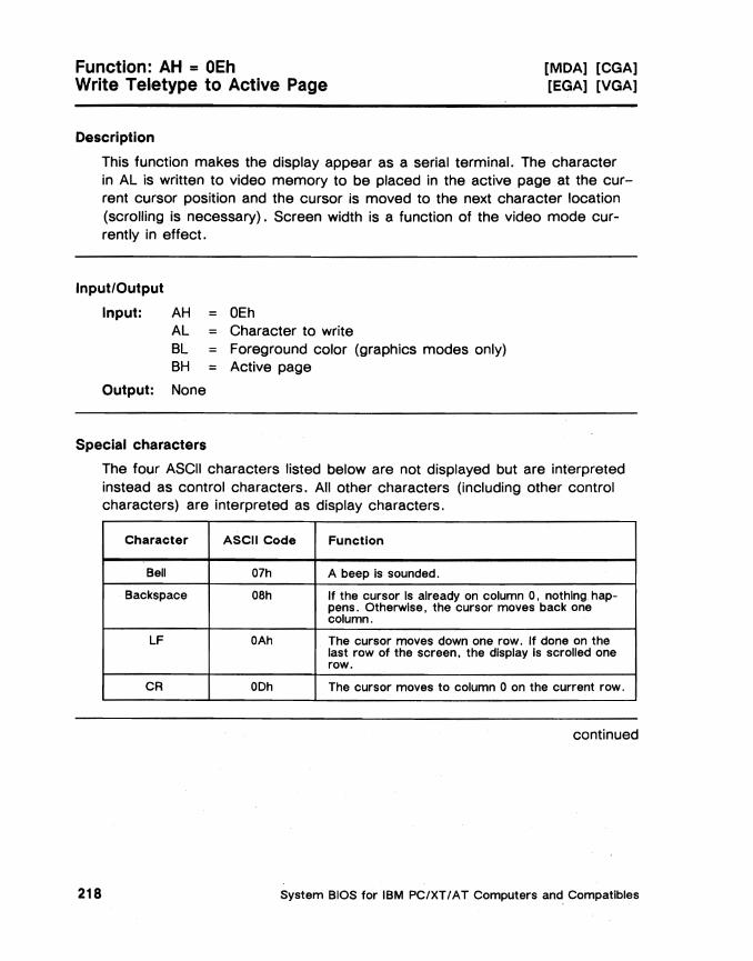
Function: AH = OEh [MDA] [eGA] Write Teletype to Active Page [EGA] [VGA]
Description
This function makes the display appear as a serial terminal. The character in AL is written to video memory to be placed in the active page at the current cursor position and the cursor is moved to the next character location (scrolling is necessary). Screen width is a function of the video mode currently in effect.
Input/Output
Input: AH = OEh AL = Character to write BL = Foreground color (graphics modes only) BH = Active page
Output: None
Special characters
The four ASCII characters listed below are not displayed but are interpreted instead as control characters. All other characters (including other control characters) are interpreted as display characters.
Character ASCII Code Function
Bell 07h A beep is sounded.
Backspace OSh If the cursor Is already on column O. nothing happens. Otherwise. the cursor moves back one column.
LF OAh The cursor moves down one row. If done on the last row of the screen, the display is scrolled one row.
CR OOh The cursor moves to column 0 on the current row.
continued
System BIOS for IBM PC/XT/AT Computers and Compatibles 218

Function: AH ... OEh [MDA] [eGA] Write Teletype to Active Page, Continued [EGA] [VGA]
Additional information
• When working in the active page, this function allows a character to be printed at the current cursor position. After printing the character, it moves the cursor to the right one space. It then wraps the cursor to the next line. Scrolling the screen up one line requires that the cursor be moved past the lower right corner of the screen.
• In CGA text mode, characters can be written to any legal display page, no matter which page is active.
• Compare this function with INT 10h, Function 13h.
• This is the best function to use for simple output.
DOS uses
DOS uses this function in the console driver for writing operating system text and messages to the screen.
This function does not, however, allow the attribute of a text character to be selected. To define an attribute for a character written to the screen:
1. write the ASCII blank character (20h) having the desired attribute to the current position using Function 09h, and
2. write the desired character using Function OEh.
With this method, the user does not have to provide for line wrapping and screen scrolling, but can allow the BIOS to control line wrap and screen scroll.
INT 10h Video 'Service 219
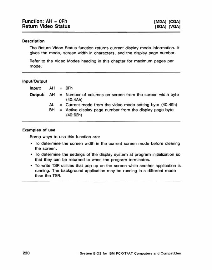
Function: AH = OFh [MDA] [eGA] Return Video Status [EGA] [VGA]
Description
The Return Video Status function returns current display mode information. It gives the mode. screen width in characters. and the display page number.
Refer to the Video Modes heading in this chapter for maximum pages per mode.
Input/Output
Input: AH = OFh
Output: AH = Number of columns on screen from the screen width byte (40:4Ah)
AL = Current mode from the video mode setting byte (40:49h) BH = Active display page number from the display page byte
(40:62h)
Examples of use
Some ways to use this function are:
• To determine the screen width in the current screen mode before clearing the screen.
• To determine the settings of the display system at program initialization so that they can be returned to when the program terminates.
• To write TSR utilities that pop up on the screen while another application is running. The background application may be running in a different mode than the TSR.
System BIOS for IBM PC/XTI AT Computers and Compatibles 220
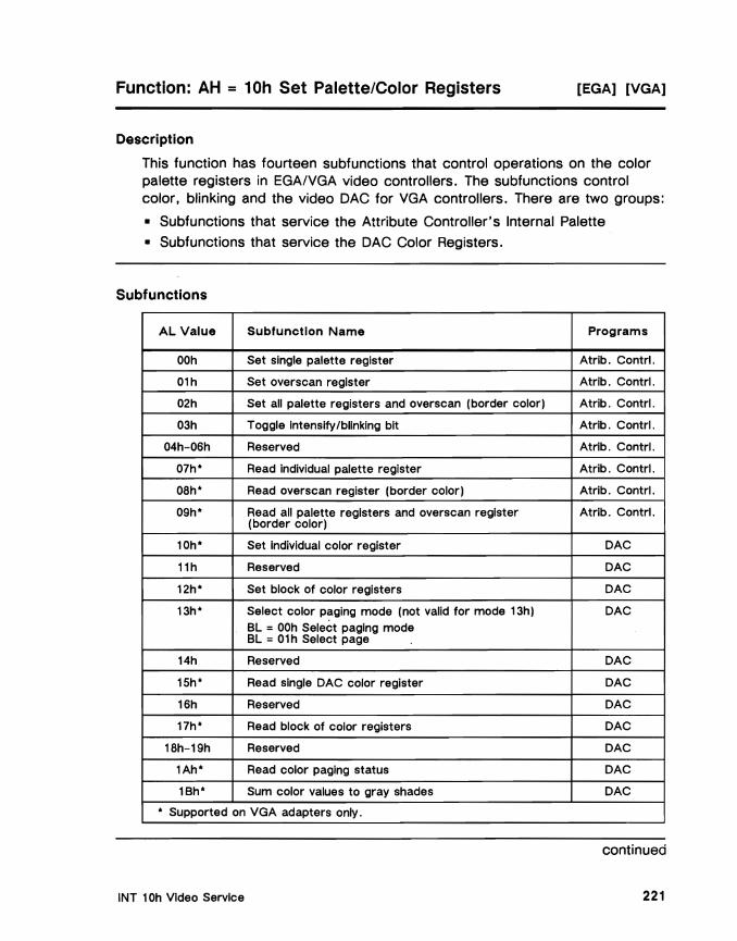
Function: AH = 10h Set Palette/Color Registers [EGA] [VGA]
Description
This function has fourteen subfunctions that control operations on the color palette registers in EGAIVGA video controllers. The subfunctions control color, blinking and the video DAC for VGA controllers. There are two groups:
• Subfunctions that service the Attribute Controller's Internal Palette
• Subfunctions that service the DAC Color Registers.
Subfunctions
AL Value Subfunction Name Programs
OOh Set single palette register Atrib. Contrl.
01h Set overscan register Atrlb. Contrl.
02h Set all palette registers and overscan (border color) Atrlb. Contrl.
03h Toggle Intensify/blinking bit Atrlb. Contrl.
04h-06h Reserved Atrlb. Contrl.
07h* Read individual palette register Atrib. Contrl.
08h* Read overscan register (border color) Atrib. Contrl.
09h* Read all palette registers and overscan register Atrib. Contrl. (border color)
10h* Set Individual color register DAC
11 h Reserved DAC
12h* Set block of color registers DAC
13h* Select color paging mode (not valid for mode 13h) DAC BL =OOh Select paging mode BL =01h Select page
14h Reserved DAC
15h* Read single DAC color register DAC
16h Reserved DAC
17h* Read block of color registers DAC
18h-19h Reserved DAC
1Ah* Read color paging status DAC
1Bh* Sum color values to gray shades DAC
* Supported on VGA adapters only.
continued
INT 10h Video Service 221

Function: AH = 10h Set Palette/Color Registers, Continued [EGA] [VGA]
Subfunction: AL = OOh Set single palette [EGA] [VGA]
This subfunction sets a single color value in the Attribute Controller's 16value internal palette. For VGA mode 13h (i.e, 2S6-color graphics), this subfunction exits without processing.
Input: AH = 10h AL = DOh set single palette BH = New color value BL = Palette register
Output: None
Subfunction: AL = 01 h Set overscan register [EGA] [VGA]
This subfunction sets the overscan color (screen border) for the current video modes.
Input: AH = 10h AL = 01h BH = Color value to set
Output: None
continued
System BIOS for IBM PC/XT I AT Computers and Compatibles 222

Function: AH = 10h Set Palette/Color Registers, Continued [EGA] [VGA]
Subfunction: AL = 02h Set all palette registers and overscan (border color) [EGA] [VGA]
This subfunction sets all 16 Attribute Controller internal palette registers, as well as the overscan register (11 h), to the values pointed to by the 17-byte table by ES:BX. This function exits without processing if the current mode is VGA mode 13h (i.e., 256-color graphics).
Input: AH = 10h AL = 02h ES:DX = Pointer to 17-byte table, where:
Byte 16 = Overscan value (border color) Bytes 15-0 = Palette values
Output: None
Subfunction: AL =03h Toggle intensity/blink bit [EGA] [VGA]
This subfunction sets either the background intensity or the foreground blinking for all color modes displayed by EGA and VGA adapters.
Input: AH = 10h AL = 03h BL = OOh Enable background intensity
= 01 h Enable foreground blinking
Output: None
Subfunctions: AL = 04h to 06h
These subfunctions are reserved.
continued
INT 10h Video Service 223

Function: AH = 10h Set Palette/Color Registers, Continued [EGA] [VGA]
Subfunction: AL = 07h Read individual palette register [VGA]
This subfunction reads the color value of the register input into BL and returns that value in BH.
Input: AH = 10h AL = 07h BL = Palette register to be read (Range OOh -OFh)
Output: BH = Value read
Subfunction: AL = OSh Read overscan register (border color) [VGAl
This subfunction reads the color value stored in the overscan register of the current color palette. This value defines the current border color.
Input: AH = 10h AL 08h
Output: BH = Value read
Subfunction: AL = 09h Read all palette registers and overscan register (border color) [VGAl
This subfunction reads the contents of the current palette register and the overscan register and outputs the contents to a table pointed to by ES:DX. The table pointed to by ES:DX must be 17 bytes long.
Input: AH = 10h AL = 09h ES:DX = Pointer to 17-byte buffer for return values
Output: ES:DX = Pointer to 17-byte table destination, where: Byte 16 = Overscan value (border color) Bytes 15-0 = Register color values
continued
System BIOS for IBM PC/XTIAT Computers and Compatibles 224

Function: AH = 10h Set Palette/Color Registers, Continued [EGA] [VGA]
Subfunction: AL = 1OhSet individual color register [VGA]
This subfunction reads in a table of RGB color values from the area pointed to by ES:DX. The number of the first DAC color register to set is specified in BX. The total number of color registers to set is specified in CX. Each red, green, and blue entry must be one byte long.
Bits 7-6 are don't care bits. Bits 5-0 are set as 3Fh (most intense) to OOh (off).
Input: AH = 10h AL = 10h BX = Color register to set CH = Green value to set, where:
Bits 7-6 = Reserved Bits 5-0 = 3Fh Most intense; OOh = Off (black)
CL = Blue value to set, where: Bits 7-6 = Reserved Bits 5-0 =3Fh Most intense: OOh = Off (black)
DH = Red value to set, where: Bits 7-6 = Reserved Bits 5-0 =3Fh Most intense; OOh = Off (black)
Output: None
With gray scale summing selected, the weighted sum gray shade value is calculated and saved to each of the three RGB parts of the color register. See INT 1Oh, Function 1 Oh, subfunction 1 Bh for a description of this calculation.
Subfunction: AL = 11 h
This subfunction is reserved.
continued
INT 10h Video Service 225
Function: AH = 10h Set Palette/Color Registers, Continued [EGA] [VGA]
Subfunctlon.: AL = 12h Set block of color registers [VGA]
This subfunction sets a consecutive series of DAC color registers. Input the number of the first color register to set in BX, the number of color registers to set in CX, and the pointer to the table of color values in ES:DX.
Input: AH = 10h At = 12h BX = First color register to set CX = Number of color registers to set ES:DX = Pointer to table of color values. Table format is red,
green, blue, red, green, blue
Output: None
With gray scale summing selected, the weighted sum gray shade value is calculated and saved to each of the three RGB parts of the color register. See INT 10h, Function 10h, subfunction 1Bh for a description of this calculation.
continued
System BIOS for IBM PC/XT/AT Computers and Compatibles 226
Function: AH = 10h Set Palette/Color Registers, Continued [EGA] [VGA]
Subfunc'tion: AL = 13h Select color paging mode [VGA]
The DAC chip contains 256 color registers. In all modes except mode 13h (i.e., 256-color graphics), the DAC color registers can be logically divided into four blocks, each containing 64 color registers, or into 16 blocks, each containing 16 color registers.
Depending on the value placed in BL, this subfunction performs two operations:
• When BL = OOh, the value placed in BH selects whether the 256 DAC color registers will be logically divided into four blocks of 64 color registers or into 16 blocks of 16 color registers.
• When BL = 01 h, the value placed in BL selects an individual block of color registers. When in four-block mode, the allowable range for BH is 00h-03h. When in 16-block mode, the allowable, range for BH is OOh-OFh.
Input: AH = 10h AL = 13h BH OOh Set 4 blocks of 64 registers
= 01 h Set 16 blocks of 16 registers BL = ~Oh Set block mode
or BL = 01 h Select individual block BH 00h-03h for 4-block mode
OOh-OFh for 16-block mode
Output: None
The Set single palette subfunction (AH = 1Oh, AL = OOh) defaults to the 64 register/block mode, initializing only the first block of 64 color registers. Alternate blocks of color registers are initialized through the Select paging mode subfunction (AH = 10h, AL = 13h, BL = OOh). Alternate blocks of color registers must be initialized for the Select page subfunction (AH = 1Oh, AL = 13h, BL = 01h) to operate properly.
continued
INT 10h Video Service 227
Function: AH = 10h Set Palette/Color Registers, Continued [EGA] [VGA]
Subfunction: AL =14h
This subfunction is reserved.
Subfunction: AL = 15h Read single DAC color register [VGAl
This subfunction reads an individual DAC color register.
Input: AH = 10h AL = 15H BX = Color register to read
Output: CH = Green value CL = Blue value DH = Red value
Subfunction: AL = 16h
This subfunction is reserved.
Subfunction: AL = 17h Read block of color registers [VGAl
This subfunction reads a block of DAC color registers to the buffer area pointed to by ES:DX.
Input: AH = 10h AL = 17h BX = DAC color register that begins block CX = Total number of color registers to read ES:DX = Pointer to buffer to save register information in.
(3 bytes per color register). Format as red byte, green byte, blue byte ...
Output: ES:DX = Pointer to values read
Subfunctions: AL = 18h to 19h
These subfunctions are reserved.
continued
System BIOS for IBM PCIXTIAT Computers and Compatibles 228

Function: AH = 10h Set Palette/Color Registers, Continued [EGA] [VGA]
Subfunction: AL = 1Ah Read color paging status [VGA]
This subfunction returns the current color paging mode as well as the current color page within this mode. See INT 1Oh, Function 1 Oh, subfunction 13h, Select color paging mode.
Input: AH AL
= 10h 1Ah
Output: BH BL
= = =
Current page Current paging mode OOh (4 pages of 64 registers) 01 h (16 pages of 16 registers)
Subfunction: AL = 1 Bh Sum color values to gray shades [VGA]
This subfunction reads the red, green, and blue values stored in the specified color registers and performs the following weighted sum:
Gray Shade = 30% red + 59% green + 11 % blue
The resulting red, green, and blue values are written to the specified color registers. The original contents of each register are not retained.
Input: AH = 10h AL 1Bh BX = Color register to start with CX = Count of how many to sum
Output: None
INT 10h Video Service 229

Function: AH = 11 h Load Character Generator [EGA] [VGA]
Description
The Load Character Generator function consists of fifteen subfunctions, all of which, in one way or another, permit the loading and/or enabling of text mode and graphics mode character generators (fonts).
Load Character Generator subfunctions
The Load Character Generator subfunctions are invoked by passing the proper parameter in the AL register. The subfunctions are:
AL Value Subfunction Name
OOh Load user text mode font
01h Load ROM 8x14 text mode font
02h Load ROM 8x8 double dot text mode font
03h Set block specifier (text modes only)
04h* Load 8x16 ROM text mode font
10h Load user text mode font (after mode set)
11 h Load ROM 8x14 text mode font (after mode set)
12h Load ROM 8x8 double dot text mode font (after mode set)
l4h* Load 8x16 ROM text mode font (after mode set)
20h Set user graphics character pointer at INT 1 Fh (8x8 font)
21h Set user graphics character pointer at INT 43h
22h Use ROM 8x14 font for graphics
23h Use ROM 8x8 double dot font for graphics
24h* Use ROM 8x16 font for graphics
30h Get font pointer information
* Supported on VGA adapters only.
continued
System BIOS for IBM PC/XT/AT Computers and Compatibles 230
Function: AH = 11h Load Character Generator, Continued [EGA] [VGA]
Subfunctions: AL = OOh, 01 h, 02h, 03h, 04h [EGA] [VGA]
As a group. subfunctions OOh - 04h allow the user to load character font sets into memory map 2. the area of video memory where the BIOS references text mode character generators. There are slight differences in the way these functions are supported on EGA and VGA adapters.
The following facts apply:
• On EGA adapters. this subfunction performs a mode set. resetting the video environment but preserving the contents of the video buffer.
• Subfunction 04h is not supported on EGA subsystems. • On VGA adapters. no mode set occurs. Scan lines per character. number
of character rows. buffer length. and cursor size are not recalculated.
• To prevent unpredictable results, the user-defined font loaded here must occupy a character box size that is close in size to the one employed by the current mode.
Subfunction: AL = OOh Load user text mode font [EGA] [VGA]
This subfunction loads a user-defined font into the memory map 2 block specified in BL. The user font must be stored in a table pointed to by ES:BP, with the ASCII character 10 or the first character specified in OX. This subfunction is for fonts in text display mode. For fonts in graphics mode. see INT 10h. Function 11h. subfunctions 20h-24h.
Inp....t: AH = 11h AL = OOh BH = Number of bytes per character BL = Block to load (valid values are OOh - 07h) CX = Number of characters to store OX = Character 10 of first character in ES:BP table ES:BP = Pointer to the user table
Output: None
continued
INT 10h Video Service 231
Function: AH = 11 h Load Character Generator, Continued [EGA] [VGA]
Subfunction: AL = 01h Load ROM 8x14 text mode font [EGA] [VGA]
This subfunction loads the ROM-resident 8x14 font into the memory map 2 block indicated in BL. Use this subfunction to override the BIOS default character block location for 8x14 character video modes. For fonts in graphics mode, see INT 1Oh, Function 11 h, subfunctions 20h-24h.
Input: AH = 11h AL = 01h BL = Block to load (valid values are OOh - 07h)
Output: None
Subfunction: AL = 02h Load 8x8 double dot text mode font [EGA] [VGA]
This subfunction loads the ROM-resident 8x8 font into the character block indicated in BL. Use this subfunction to override the BIOS default character block location for 8x8 character video modes. For fonts in graphics mode, see INT 1Oh, Function 11 h, subfunctions 20h-24h.
Input: AH = 11h AL = 02h BL = Block to load (valid values are OOh - 07h)
Output: None
continued
System BIOS for IBM PC/XT/ AT Computers and Compatibles 232

Function: AH = 11h Load Character Generator, Continued [EGA] [VGA]
Subfunction: AL = 03h Set block specifier (text modes only) [EGA] [VGA]
EGA- and VGA-compatible hardware allows the user to display up to 512 text mode characters at a time. However, in text modes, all character font bit patterns are ~tored in 8K blocks in video memory map 2. Each 8K block can store up to 256 characters. In order to display 512 text mode characters special steps need to be taken to allow end user software to select between either of two possible 8K character blocks.
This supfunctionsets up the video hardware so that bit 3 of each text mode attribute byte can select between either of two memory map 2 character blocks, thus allowing up to 512 characters to be displayed in any text mode. Characters are selected according to the rules below:
• The value of bits 4, 1, and 0 of BL set by this subfunction indicates the first character block; the value of bits 5, 3, and 2 in BL indicates the second character block.
• The value of bit 3 of each character attribute byte determines from which character block a given ASCII character will be selected.
• When bit 3 = 0, the character is selected from the block defined by bits 4, 1, and a input into BL.
• When bit 3 = 1, the character is selected from the block defined by bits 5,3, and 2 of BL.
~ If bits 4, 1, and 0 = bits 5, 3, and 2, then bit 3 of the character attribute byte toggles foreground intensity on or off. When two character blocks are selected, Function AX = 1000h BX =0712h will ensure that eight consistent color planes are set.
Note: To make a loaded character block active, this subfunction must be run after any load character block subfunction.
Input: AH = 11 h AL = 03h BL = Select character block (see description above)
Output: None
continued
INT 10h Video Service 233

Function: AH = 11h Load Character Generator, Continued [EGA] [VGA]
Subfunction: AL = 04h Load 8x16 ROM text mode font [VGA]
This subfunction loads the ROM-resident 8x16 font into the character block indicated in BL. Use this subfunction to override the BIOS default character block for 8x16 character block modes. For fonts in graphics mode, see INT 1Oh, Function 11 h, subfunctions 20h-24h.
Input: AH = 11h AL = 04h BL = Block to load (valid values are 0-7)
Output: None
Subfunctions: AL = 10h, 11 h. 12h. 14h [EGA] [VGA]
Subfunctions AL = 1Oh, 11 h, 12h, and 14h, respectively, are identical to subfunctions AL = OOh, 01 h, 02h, and 04h except for the following:
• Page 0 is active, • the bytes per character (points) are recalculated, • the number of rows is recalculated,
• the display buffer length is calculated, and
• the following CRTC registers are reprogrammed:
• Index 09h Maximum scan line index
• Index OAh Cursor start index • Index OBh Cursor end index
• Index 12h Vertical displacement end index
• Index 14h Underline location (mode 07h only)
continued
System BIOS for IBM PC/XT/AT Computers and Compatibles 234

Function: AH = 11 h Load Character Generator, Continued [EGA] [VGA]
Subfunction: AL =10h Load user text mode font (after mode set) [EGA] [VGA]
This subfunction loads the user character set defined in the table pointed to by ES: BP to the character block indicated BL.
Input: AH = 11 h AL = 10h BH = Number of bytes per character BL Block to load (valid values are 0-7) CX = Number of characters to store OX = Character 10 of first character in ES:BP table ES:BP = Pointer to table
Output: None
The registers programmed by subfunction 10h are a subset of all EGAIVGA CRTC registers. Because of this, the font downloaded by this subfunction must be relatively close in size to the default font associated with the current video mode. To prevent unpredictable results, these subfunctions should only be called after a call to INT 10h, AH = OOh Set Video Mode.
Subfunction: AL = 11 h Load ROM 8x14 text mode font (after mode set) [EGA] [VGA]
This subfunction loads the ROM 8x14 font into the character block indicated in BL. Bytes/characters (point size), number of display rows, cursor and underline parameter, and display buffer length are recalculated. Use this subfunction to override the BIOS-defined font for the text mode in question.
Input: AH = 11 h AL = 11 h BL = Block to load (valid values are 0-7)
Output: None
The registers programmed by subfunction 11 h are a subset of all EGAIVGA CRTC registers. Because of this, the font downloaded by this subfunction must be relatively close in size to the default font associated with the current video mode. To prevent unpredictable results, these subfunctions should only be called after a call to INT 1Oh. AH = OOh Set Video Mode.
continued
INT 10h Video Service 235
Function: AH = 11 h Load Character Generator, Continued [EGA] [VGA]
Subfunction: AL =12h Load ROM 8x8 double dot text mode font [EGA] [VGA]
This subfunction loads the ROM 8x8 font into the character block indicated in BL. Bytes/character (point size), number of display rows, cursor and underline parameters, and display buffer length are recalculated. Use this subfunction to override the BIOS-defined font for the text mode in question.
Input: AH AL BL
=
=
11 h 12h Block to load
Output: None
The registers programmed by subfunction 12h are a subset of all EGAIVGA CRTC registers. Because of this, the font downloaded by this subfuhction must be relatively close in size to the default font associated with the current video mode. To prevent unpredictable results, these subfunctions Should only be called after a mode set call (i. e., INT 1Oh, AH = OOh Set Video Mode) .
Subfunction: AL =14h Load 8x16 ROM text 1l10de font [VGA]
This subfunction loads the ROM 8x16 font into the character block indicated in BL. Bytes/character (point size), number of display rows, cursor and underline parameters, and display buffer length are recalculated. Use this subfunction to override the BIOS-defined font for the text mode in question.
Input: AH 11 h AL 14h BL = Block to load
Output: None
The 8x16 text mode font is not available in EGA adapters. As such, the registers programmed by subfunction 14h are a subset of all VGA CRTC registers. Because of this, the font downloaded by this subfunction must be relatively close in size to the default font associated with the current video mode. To prevent unpredictable results, these subfunctions should only be called after a mode set call (I.e., INT 1Oh, AH = OOh Set Video Mode).
continued
System BIOS for IBM PC/XT/AT Computers and Compatibles 236

Function: AH = 11h Load Character Generator, Continued [EGA] [VGA]
Subfunctions: AL = 20h, 21 h, 22h, 23h, 24h [EGA] [VGA]
Subfunctions AL = 20h, 21 h, 22h, 23h, and 24h all deal with fonts that are used in graphics modes. For functions that deal with fonts in text display mode, see INT 10h, Function 11 h, subfunctions OOt¥-+4h-.
To prevent unpredictable results, subfunctions AL = 20h, 21 h, 22h, 23h, and 24h should be called only immediately after a video mode is set (See INT 1Oh, AH =OOh Set Video Mode, AL = mode to select).
Subfunction: AL = 20h Set user graphics font pointer at INT 1 Fh (8x8 font) [EGA] [VGA]
This subfunction sets the graphics font pointer to the vector contained in INT 1 Fh. The INT1Fh vector is specified in ES:BP. The font table pointed to is used by applications programs running on EGA or VGA adapters that are set to modes 04h - 06h, the CGA graphic modes. The graphics character set loaded can contain bit patterns for ASCII characters 80h-FFh.
Input: AH = 11h AL = 20h ES:BP = User graphics font pointer
(INT 1Fh is set to the vector contained in ES:BP)
Output: None
• The character generators for all graphics modes are contained within the video BIOS. The ROM BIOS-based character generators for graphics VGA modes ODh to 13h contain all 256 ASCII characters.
• The character generators for graphics modes 04h, 05h, and 06h, (CGAcompatible graphics modes), contain only the first 128 ASCII characters. The remaining 128 ASCII characters (extended ASCII characters 80h-FFh) may be supplied by the user. All user-supplied character sets must be vectored to a memory location pointed to by INT 1 Fh. In general, these user-supplied character sets are built into an 8x8 character box.
• The DOS command GRAFTABL loads a graphic table which allows modes 04h, 05h, and 06h to display extended ASCII characters. Vectoring INT 1Fh to point to the DOS GRAFTABL graphics table is the usual method of providing user-supplied extended ASCII characters.
continued
INT 10h Video Service 237
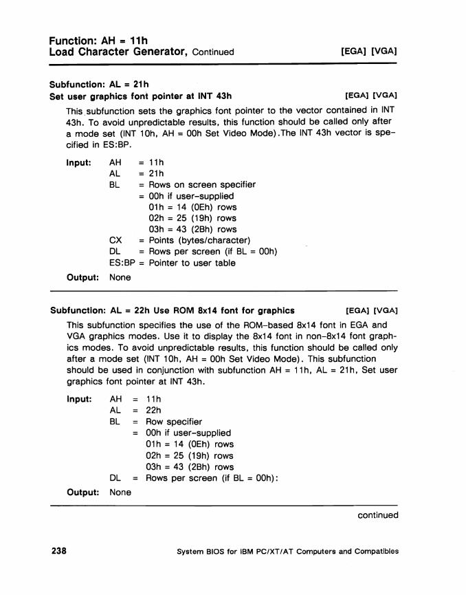
Function: AH = 11 h Load Character Generator, Continued [EGA] [VGA]
Subfunction: AL = 21 h Set user graphics font pointer at INT 43h [EGA] [VGA]
This. subfunction sets the graphics font pointer to the vector contained in INT 43h. To avoid unpredictable results, this function should be called only after a mode set (INT 10h, AH = OOh Set Video Mode) .The INT 43h vector is specified in ES:BP.
Input: AH = 11h AL = 21h BL = Rows on screen specifier
= ~Oh if user-supplied 01 h = 14 (OEh) rows 02h = 25 (19h) rows 03h = 43 (2Bh) rows
CX = Points (bytes/character) DL = Rows per screen (if BL = OOh) ES:BP = Pointer to user table
Output: None
Subfunction: AL =22h Use ROM 8x14 font for graphics [EGA] [VGA]
This subfunction specifies the use of the ROM-based 8x14 font in EGA and VGA graphics modes. Use it to display the 8x14 font in non-8x14 font graphics modes. To avoid unpredictable results, this function should be called only after a mode set (INT 10h, AH = OOh Set Video Mode). This subfunction should be used in conjunction with subfunction AH = 11 h, AL = 21 h, Set user graphics font pointer at INT 43h.
Input: AH = 11 h AL 22h BL Row specifier
= OOh if user-supplied 01 h = 14 (OEh) rows 02h = 25 (19h) rows 03h = 43 (2Bh) rows
DL = Rows per screen (if BL = OOh):
Output: None
continued
System BIOS for IBM PC/XT/AT Computers and Compatibles 238

Function: AH = 11 h Load Character Generator, Continued [EGA] [VGA]
Subfunction: AL = 23h Use ROM 8x8 double dot font for graphics [EGA] [VGA]
This subfunction specifies the use of the ROM-based 8x8 font in EGA and VGA graphics modes. Use it to display the 8x8 font in non-8x8 font graphics modes. To avoid unpredictable results, this function should be called only after a mode set (INT 1Oh, AH = ~Oh Set Video Mode). This subfunction should be used in conjunction with subfunction AH = 11h, AL = 21h, Set user graphics font pointer at INT 43h.
Input: AH = 11 h AL = 23h BL = Row specifier
= OOh if user-supplied 01 h = 14 (OEh) rows 02h = 25 (19h) rows 03h = 43 (2Bh) rows
DL = Rows per screen (if BL = OOh)
Output: None
Subfunction: AL = 24h Use ROM 8x16 font for graphics [VGAl
This subfunction specifies the use of the ROM-based 8x16 font in VGA graphics modes. Use it to override to display the 8x16 font in non-8x16 font graphics modes. To avoid unpredictable results, this function should be called only after a mode set (INT 10h, AH = OOh Set Video Mode). This subfunction should be used in conjunction with subfunction AH = 11 h, AL = 21 h, Set user graphics font pointer at INT 43h.
Input: AH = 11 h AL = 24h BL = Row specifier
= OOh if user-supplied 01 h = 14 (OEh) rows 02h = 25 (19h) rows 03h = 43 (2Bh) rows
DL = Rows per screen (if BL = OOh)
Output: None
continued
INT 10h Video Service 239

Function: AH = 11 h Load Character Generator, Continued [EGA] [VGA]
Subfunction: AL =30h Get font pointer information [EGA] [VGAl
This subfunction returns font pointer information. The pointer information desired is requested in the BH register. To avoid unpredictable results, this subfunction should be issued immediately after a mode set.
Input: AH = 11 h AL = 30h BH = Font pointer, where:
= ~Oh Return current INT 1Fh pointer = 01 h Return current INT 43h pointer = 02h Return ROM font 8x14 pointer = 03h Return current ROM 8x8 font pointer = 04h Return current ROM 8x8 font pointer (top) = OSh Return current ROM 9x14 font alternate = 06h Return current ROM 8x16 font pointer = 07h Return current ROM 9x16 font alternate = >07h Returns all registers (including AX) preserved
Output: CX = Bytes per character DL = Maximum number of rows on screen ES:BP = Pointer to character table
System BIOS for IBM PC/XT/ AT Computers and Compatibles 240
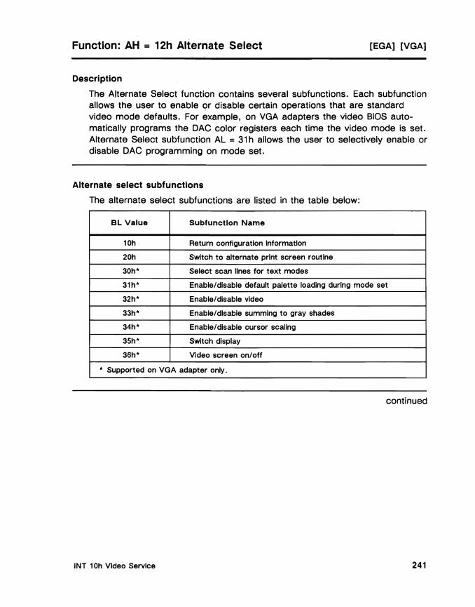
Function: AH = 12h Alternate Select [EGA] [VGA]
Description
The Alternate Select function contains several subfunctions. Each subfunction allows the user to enable or disable certain operations that are standard video mode defaults. For example, on VGA adapters the video BIOS automatically programs the DAC color registers each time the video mode is set. Alternate Select subfunction AL = 31 h allows the user to selectively enable or disable DAC programming on mode set.
Alternate select subfunctions
The alternate select subfunctions are listed in the table below:
BL Value Subfunctlon Name
10h Return configuration Information
20h Switch to alternate print screen routine
30h" Select scan lines for text modes
31h" Enable/disable default palette loading during mode set
32h" Enable/disable video
33h" Enable/disable summing to gray shades
34h" Enable/disable cursor scaling
35h" Switch display
36h" Video screen on/off
" Supported on VGA adapter only.
continued
INT 10h Video Service 241
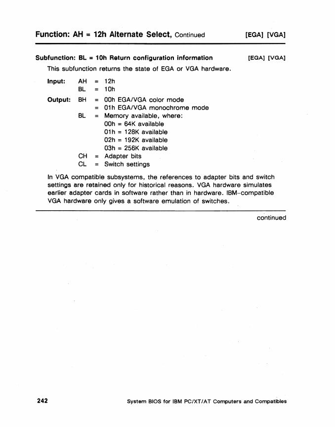
Function: AH = 12h Alternate Select, Continued [EGA] [VGA]
Subfunction: BL = 10h Return configuration information [EGA] [VGA]
This subfunction returns the state of EGA or VGA hardware.
Input: AH = 12h BL = 10h
Output: BH = OOh EGAIVGA color mode
= 01 h EGAIVGA monochrome mode BL = Memory available, where:
OOh =64K available 01 h = 128K available 02h = 192K available 03h = 256K available
CH = Adapter bits CL = Switch settings
In VGA compatible subsystems, the references to adapter bits and switch settings are retained only for historical reasons. VGA hardware simulates earlier adapter cards in software rather than in hardware. IBM-compatible VGA hardware only gives a software emulation of switches.
continued
System BIOS for IBM PC/XT/AT Computers and Compatibles 242
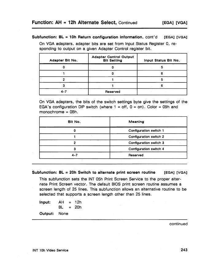
Function: AH = 12h Alternate Select, Continued [EGA] [VGA]
Subfunction: BL = 10h Return configuration information, cont'd [EGA] [VGA]
On VGAadapters, adapter bits are set from Input Status Register 0, respondingto output on a given Adapter Control register bit.
Adapter Control Output Adapter Bit No. Bit Setting Input Status Bit No.
0 0 5
1 0 6
2 1 5
3 1 6
4-7 Reserved
On VGA adapters, the bits of the switch settings byte give the settings of the EGA's configuration DIP switch (where 1 =off, 0 =on). Color = 09h and monochrome = OBh.
Bit No. Meaning
0 Configuration switch 1
1 Configuration switch 2
2 Configuration switch 3
3 Configuration switch 4
4-7 Reserved
Subfunction:BL = 20h Switch to alternate print screen routine [EGA] [VGA]
This subfunction sets the INT 05h Print Screen Service to the proper alternate Print Screen vector. The default BIOS print screen routine assumes a screen length of 25 lines. This subfunction allows an alternative routine to be selected that supports a screen length other than 25 lines.
Input: AH = 12h BL = 20h
Output: None
continued
INT 10h Video Service 243
Function: AH = 12h Alternate Select, Continued [EGA] [VGA]
Subfunction: BL =30h Select scan lines for text modes [EGA] [VGA]
This subfunction sets the number of scan lines to be displayed in text modes. By default, the VGA BIOS sets all text modes to 400 scan lines as part of the power-on self test and initialization (POST) process.
Input: AH = 12h AL = Number of scan lines, where
OOh = 200 scan lines 01 h =350 scan lines 02h =400 scan lines
BL = 30h
Output: AL = 12h Function is supported
= OOh VGA not active
• The number of scan lines indicated in AL will take effect upon the next mode set.
• The VGA BIOS loads the font associated with the mode/scan line combination upon the next mode set.
• 200-line scan modes are double-scanned. Each video line is painted twice before the next new line is begun.
Subfunction: BL = 31 h Enable/disable default palette loading during set mode [VGAl
If AL = 01 h is selected, no updates are made to the overscan color register, the attribute color registers or the DAC color registers when a video mode is set.
Input: AH = 12h AH = OOh AL = OOh Enable default palette loading
= 01 h Disable default palette loading BL = 31h
Output: AL = 12h Function is supported
continued
System BIOS for IBM PC/XT I AT Computers and Compatibles 244
Function: AH = 12h Alternate Select, Continued [EGA] [VGA]
SubfuncUon: BL = 32h Enable/disable video [VGAl
This subfunction enables/disables the video I/O port regenerator and the display buffer address decoder for the currently active video monitor.
Input: AH = 12h AL = OOh Enable video
= 01 h Disable video BL = 32h
Output: AL = 12h Function is supported
Subfunction: BL = 33h Enable/disable summing to gray shades [VGAl
This subfunction enables/disables gray scale summing that occurs during the Set Video Mode Function (AH = OOh) and during the Set Palette Registers Function (AH = 10h) for the display that is currently active.
Input: AH = 12h AL OOh Enable summing
= 01 h Disable summing BL = 33h
Output: AL = 12h Function is supported
Subfunction: BL = 34h Enable/disable cursor scaling [VGAl
When cursor scaling is enabled (which is the power-on default), cursor start and end information is scaled to the current character height. See INT 1Oh, AH = 01 h Set Text Mode Cursor Size for more information on setting cursor type.
Input: AH = 12h AL = ~Oh Enable cursor scaling
= 01 h Disable cursor scaling BL = 34h
Output: AL = 12h Function is supported
continued
INT 10h Video Service 245
Function: AH = 12h Alternate Select, Continued [EGA] [VGA]
Subfunction: BL = 3Sh Switch display [VGAl
This subfunction permits switching between the system video and an adapter video ROM. When there is a conflict between the system video and an adapter video (i.e .• overlapping usage of the BIOS data area and/or hardware capabilities). the adapter video is the power-up default primary video. The system board video remains inactive until switching has been enabled.
To be able to switch. the Enable/disable video subfunction (AH = 12h. BL = 32h) must be supported by both the adapter and the system board.
• To enable video switching. first call with BL = 35h and AL = OOh to disable the adapter video. then call with AL = 01 h to enable system board video.
• Once switching has been enabled. all subsequent switches are done through AL = 02h disable active video and AL = 03h enable inactive video.
Input: AH = 12h AL = OOh Turn off initial video adapter. The user must establish
a 128-byte save area pointed to by ES:DX = 01 h Turn on initial system board video = 02h Disable active video. The user must have a save
buffer pointer in ES:DX = 03h Enable inactive video. The user must have a pointer
in ES:DX to a previously filled save buffer BL = 35h ES: DX = Pointer to a 128-byte save buffer area
Output: AL = 12h Function is supported
When there is no conflict between the system video and an adapter video board, both video devices are active and use of this subfunction is not necessary.
Subfunction: BL = 36h Video screen on/off [VGAl
This subfunction turns the video screen on or off.
Input: AH = 12h AL = 01 h Screen off
= OOh Screen on BL = 36h
Output: AL = 12h Function is supported
System BIOS for IBM PC/XT IAT Computers and Compatibles 246
Function: AH = 13h Write String [MDA] [CGA] [EGA] [VGA]
Description
The Write String function operates similarly to Write Teletype to Active Page Function (AH = OEh), except that an entire string is handled with each call. The AL register contains two single-bit fields differentiated as follows:
If ••• Then •.•
AL Bit 0 = 1 the cursor remains at the last character written.
AL Bit 0 = 0 the cursor Is restored to where It was before the write string operation began.
AL Bit 1 = 1 each string character to be displayed Is followed by Its attribute.
AL Bit 1 = 0 carriage return, line feed, backspace, and bell are Interpreted as commands rather than as printable characters. The string contains only display characters, and the attribute Is taken from the BL register.
Input/Output
Input: AH = 13h ES:BP = Pointer to start of string BH = Page number (for text modes) BL = Attribute for characters (graphics modes) CX = Length of string (attributes don't count) DX = Starting cursor position (DH = row, DL = column) AL = OOh Cursor not moved.
= 01h Cursor is moved. = 02h Cursor not moved (text mode only) = 03h Cursor is moved (text mode only)
Output: None
Functions: AH = 14h- 19h Reserved
INT 10h Video Service 247
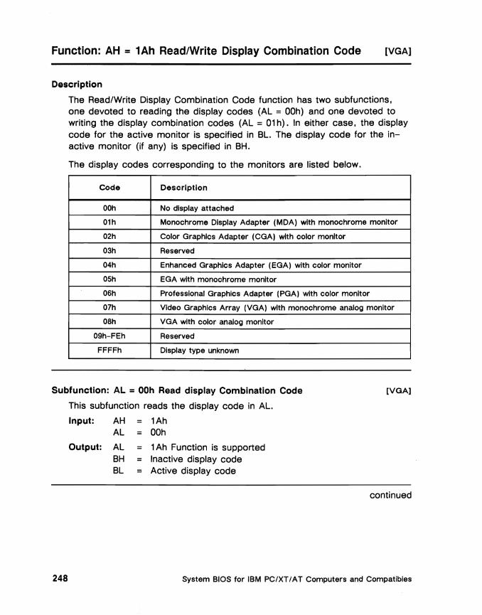
Function: AH = 1Ah Read/Write Display Combination Code [VGA]
Description
The Read/Write Display Combination Code function has two subfunctions, one devoted to reading the display codes (AL = OOh) and one devoted to writing the display combination codes (AL = 01 h). In either case, the display code for the active monitor is specified in BL. The display code for the inactive monitor (if any) is specified in BH.
The display codes corresponding to the monitors are listed below.
Code Description
OOh No display attached
01h Monochrome Display Adapter (MDA) with monochrome monitor
02h Color Graphics Adapter (CGA) with color monitor
03h Reserved
04h Enhanced Graphics Adapter (EGA) with color monitor
OSh EGA with monochrome monitor
06h Professional Graphics Adapter (PGA) with color monitor
07h Video Graphics Array (VGA) with monochrome analog monitor
OSh VGA with color analog monitor
09h-FEh Reserved
FFFFh Display type unknown
Subfunction: AL =OOh Read display Combination Code [VGAj
This subfunction reads the display code in AL.
Input: AH 1Ah AL = OOh
Output: AL BH BL
1Ah Function is supported Inactive display code Active display code
continued
System BIOS for IBM PC/XT / AT Computers and Compatibles 248

Function: AH = 1Ah Read/Write Display Combination Code, Continued [VGA]
Subfunction: AL = OOh Write Display Combination Code [VGA]
This subfunction writes the display code in AL.
Input: AH 1Ah AL = 01 h BH = Alternate display code (if any) BL = Active display code
Output: AL = 1 Ah - Function is supported
Function: AH = 1Bh Return Functionality/State Information [VGA]
Description
This function outputs a table describing the current state of the video hardware to a 40h-byte buffer location pointed to by ES:DI.
Input/Output
Input: AH = 1Bh BX = OOOOh Implementation type ES:DI = Pointer to 40h byte buffer
Output: AL = 1Bh Function successful
Functionality/state information is output to 40h-byte buffer (see description on the following page).
Error conditions
The BIOS will accept only one implementation type: BX = OOOOh. If a value other than OOOOh is input into BX, this function returns the following values:
• AH = 1Bh
• AL = OOh
• All other registers are preserved.
continued
INT 10h Video Service 249
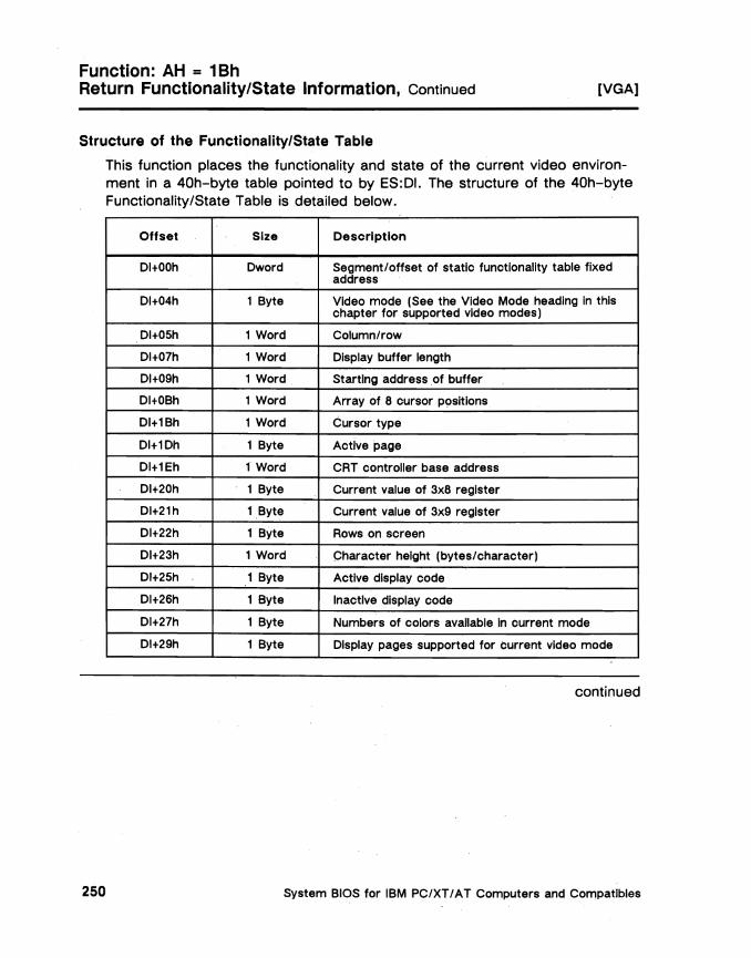
Function: AH = 1Bh Return Functionality/State Information, Continued [VGA]
Structure of the Functionality/State Table
This function places the functionality and state of the current video environment in a 40h-byte table pointed to by ES:DI. The structure of the 40h-byte Functionality/State Table is detailed below.
Offset Size Description
DI+OOh Dword Segment/offset of static functionality table fixed address
DI+04h 1 Byte Video mode (See the Video Mode heading in this chapter for supported video modes)
DI+OSh 1 Word Column/row
DI+07h 1 Word Display buffer length
DI+OSh 1 Word Starting address of buffer
DI+OBh 1 Word Array of 8 cursor positions
DI+1Bh 1 Word Cursor type
DI+1Dh 1 Byte Active page
DI+1Eh 1 Word CRT controller base address
DI+20h 1 Byte Current value of 3x8 register
DI+21h 1 Byte Current value of 3xS register
DI+22h 1 Byte Rows on screen
DI+23h 1 Word Character height (bytes/character)
DI+2Sh 1 Byte Active display code
DI+26h 1 Byte Inactive display code
DI+27h 1 Byte Numbers of colors available in current mode
DI+2Sh 1 Byte Display pages supported for current video mode
continued
System BIOS for IBM PC/XT / A T Computers and Compatibles 250

Function: AH = 1Bh Return Functionality/State Information, Continued [VGAJ
Structure of the Functionality/State Table, cont'd
Offset Size Description
DI+2Ah 1 Byte Number of scan lines In current video mode OOb =200 01b = 350 lOb =400 11 b =480 1OOb - 11111111 b = Reserved
DI+2Bh 1 Byte Primary character block OOb =Block 0 01b =Block 1 lOb =Block 2 11 b - 11111111 b =Blocks 3 to 255
DI+2Ch 1 Byte Secondary character block
OOb =Block 0 01b =Block 1 lOb =Block 2 11 b - 11111111 b =Blocks 3 - 255
DI+2Dh 1 Byte Miscellaneous state Information Bits 7-6 =Reserved Bit 5 =0 Background Intensity
=1 Blinking Bit 4 =1 Cursor emulation is active Bit 3 =1 Mode set auto palette loading disabled Bit 2 =1 Mono display is attached Bit 1 =1 Gray scale summing is active Bit 0 =1 All modes on all displays active
DI+2Eh 1 Byte Reserved
DI+2Fh 1 Byte Reserved
DI+30h 1 Byte Reserved
DI+31h 1 Byte Video memory available OOb :: 64K 01b =128K lOb =192K 11 b =256K
DI+32h 1 Byte Save pointer state information
Bits 7-6 =Reserved Bit 5 =1 Display Combination Code (DCC)
extension active Bit 4 =1 Palette override active Bit 3 =1 Graphics font override active Bit 2 =1 Text mode font override active Bit 1 =1 Dynamic save area active Bit 0 =1 512-character character set active
DI+33h-3Fh 13 Bytes Reserved
continued
INT 10h Video Service 251

Function: AH = 1Sh Return Functionality/State Information, Continued [VGA]
Structure of the Static Functionality Table
The first entry in the Functionality/State Table is a double word pointer to a 16-byte ROM-based Static Functionality Table.
The Static Functionality Table contains fixed video parameter information. The table is located at EOOO:305Fh in the BIOS. The contents of the Static Functionality Table are defined below.
Offset Value Description
OOh FFh Video modes supported Bit 7 = 1 Mode 7 s4Pported Bit 6 = 1 Mode 6 supported Bit 5 = 1 Mode 5 supported Bit 4 = 1 Mode 4 supported Bit 3 = 1 Mode 3 supported Bit 2 =1 Mode 2 supported Bit 1 = 1 Mode 1 supported Bit 0 = 1 Mode 0 supported
01h FOh Video modes supported Bit 7 =1 Mode F supported Bit 6 =1 Mode g supported Bit 5 =1 Mode 0 supported Bit 4 =0 Mode C supported Bit 3 =0 Mode B supported Bit 2 = 0 Mode A supported Bit 1 =0 Mode 9 supported Bit 0 = 0 Mode 8 supported
02h OFh Video modes slJPported Bits 7-4 =Reserved Bit 3 =1 Mode 13 supported Bit 2 =1 Mode 12 supportedBit 1 =1 Mode 11 supported Bit 0 =1 Mode 10 supported
03h-06h OOh Reserved
07h 07h Scan line modes available for text modes
Bits 7-3 =OOOOOb Reserved Bit 2 =1 400 scan lines supported Bit 1 =1 350 scan lines supported Bit 0 =1 200 scan lines supported
continued
System BIOS for IBM PC/XT/AT Computers and Compatibles 252
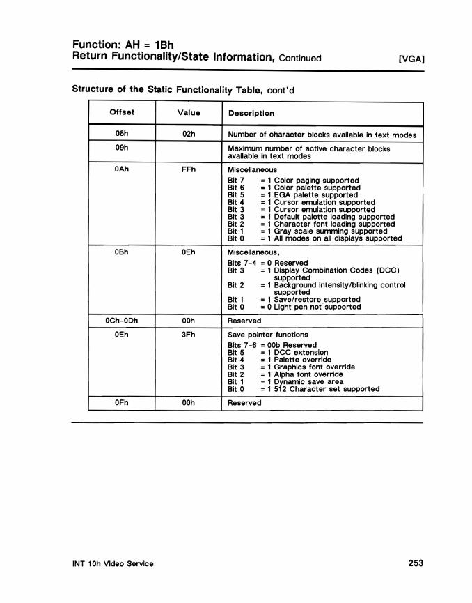
Function: AH = 1Bh Return Functionality/State Information, Continued [VGA]
Structure of the Static Functionality Table, cont'd
Offset Value Description
OSh 02h Number of character blocks available in text modes
09h Maximum number of active character blocks available in text modes
OAh FFh Miscellaneous Bit 7 = 1 Color paging supported Bit 6 =1 Color palette supported Bit 5 =1 EGA palette supported Bit 4 =1 Cursor emulation supported Bit 3 = 1 Cursor emulation supported Bit 3 =1 Default palette loading supported Bit 2 = 1 Character font loading supported Bit 1 = 1 Gray scale summing supported Bit 0 =1 All modes on all displays supported
OBh OEh Miscellaneous, Bits 7-4 = 0 Reserved Bit 3 = 1 Display Combination Codes (DCC)
supported Bit 2 =1 Background intensity /blinking control
supported Bit 1 =1 Save/restore ,supported Bit 0 = 0 Light pen not supported
OCh-ODh OOh Reserved
OEh 3Fh Save pointer functions Bits 7-6 =OOb Reserved Bit 5 = 1 DCC extension Bit 4 = 1 Palette override Bit 3 = 1 Graphics font override Bit 2 =1 Alpha font override Bit 1 =1 Dynamic save area Bit 0 =1 512 Character set supported
OFh OOh Reserved
INT 10h Video Service 253
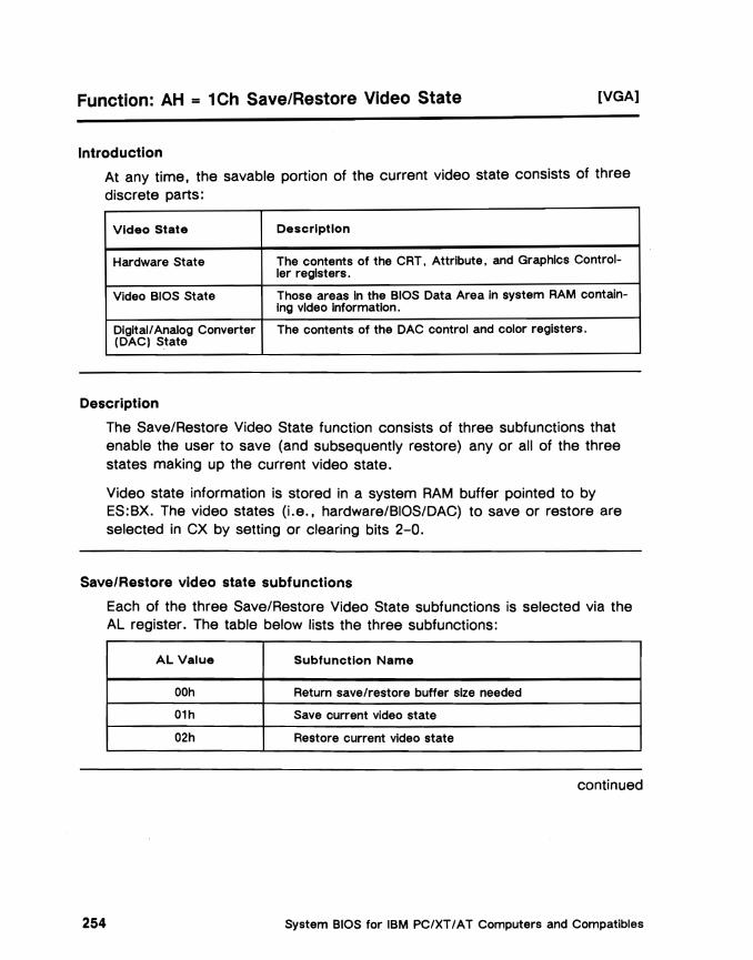
Function: AH = 1Ch Save/Restore Video State [VGA]
Introduction
At any time. the savable portion of the current video state consists of three discrete parts:
Video State Description
Hardware State The contents of the CRT. Attribute. and Graphics Controller registers.
Video BIOS State Those areas In the BIOS Data Area In system RAM contain-Ing video Information.
Digital/ Analog Converter The contents of the DAC control and color registers. (DAC) State
Description
The Save/Restore Video State function consists of three subfunctions that enable the user to save (and subsequently restore) any or all of the three states making up the current video state.
Video state information is stored in a system RAM buffer pointed to by ES:BX. The video states (i.e .• hardware/BIOS/DAC) to save or restore are selected in CX by setting or clearing bits 2-0.
Save/Restore video state subfunctions
Each of the three Save/Restore Video State subfunctions is selected via the AL register. The table below lists the three subfunctions:
AL Value Subfunctlon Name
OOh Return save/restore buffer size needed
01h Save current video state
02h Restore current video state
continued
System BIOS for IBM PC/XT / AT Computers and Compatibles 254

Function: AH = 1Ch Save/Restore Video State, Continued [VGAI
Error handling
Upon entry into the Save/Restore Video State function, the BIOS checks the parameter passed in the AL register. If it is out of range (i.e., greater than 02h), then the function returns with AL = OOh and AH preserved.
Buffer format for save/restore video state
The save buffer is composed of a 20h-byte fixed offset area followed by one, two, or three optional areas, depending on which areas (hardware/ BIOS/DAC) were specified in CX.
The 20h-byte fixed offset area contains the following information:
Offset Description
OOh Word offset of hardware save area, If saved
02h Word offset of BIOS RAM save area, If saved
04h Word offset of DAC save area, If saved
06h-1Fh Reserved
Subfunction AL = OOh Return save/restore buffer size needed [VGAl
This subfunction returns the buffer size (in 64-byte blocks) needed for any combination of the three video states that can be stored. The video state (or combination of video states) is specified in CX; the buffer size in 64-byte blocks is returned in BX.
Input: AH = 1Ch AL = OOh CX = Video state to store, where:
Bit 0 = 1 Save video hardware state Bit 1 = 1 Save video BIOS data area Bit 2 = 1 Save video DAC state and color registers Bits 3-15 = 0 Reserved
Output: AL = 1Ch Function is supported BX Buffer size block count (1 block = 64 bytes)
continued
INT 10h Video Service 255

Function: AH = 1Ch Save/Restore Video State, Continued [VGA]
[VGAlSubfunction: AL = 01 h Save current video state
This subfunction stores the video states specified in CX to a system RAM buffer area pointed to by ES:BX.
Input: AH = 1Ch AL = 01h CX = Video state to store, where:
Bit 0 = 1 Save video hardware state Bit 1 = 1 Save video BIOS data area Bit 2 = 1 Save video DAC state and color registers Bits 3-15 = 0 Reserved
ES:BX = Pointer to system RAM buffer
Output: AL = 1Ch Function is supported
Warning
Saving a video state alters the original contents of the registers or data areas involved. To maintain the current video state, execute the Restore current video state subfunction immediately after saving the video state.
Subfunction: AL = 02h Restore current video state [VGAl
This subfunction restores the video states specified in CX from the system RAM buffer area pointed to by ES:BX.
Input: AH = 1Ch AL = 02h CX = Video state to restore, where:
Bit 0 = 1 Save video hardware state Bit 1 = 1 Save video BIOS data area Bit 2 = 1 Save video DAC state and color registers Bits 3-15 = 0 Reserved
ES:BX = Pointer to previously saved system RAM buffer
Output: AL = 1Ch Function is supported
continued
System BIOS for IBM PC/XTIAT Computers and Compatibles 256

Function: AH = 1Ch Save/Restore Video State, Continued [VGAJ
Structure of hardware state save area
If bit 0 of the CX register is set and. the save video state subfunction is executed. the current hardware state is stored to the system RAM buffer pointed to by ES:BX. Executing the restore video state subfunction with the same ex and ES:BX values restores the hardware state information to the actual video hardware.
The structure of the hardware state save area is as follows:
I/O Offset Address Index Description
OOh 03C4h Sequencer Index
01h 3B4h/3D4h· CRT Controller Index
02h 03CEh Graphics Controller Index
03h 03COh Attribute Controller Index
04h 03CAh Feature Control
SEQUENCER REGISTERS
05h 03C5h 01h Clocking Mode
06h 03C5h 02h Map Mask
07h 03C5h 03h Character Map Select
08h 03C5h 04h Memory Mode
09h 03CCh OOh Miscellaneous Output
• 03B4h In Monochrome Emulation Modes 03D4h in Color Emulation Modes
continued
INT 10h Video Service 257

Function: AH = 1Ch Save/Restore Video State, Continued [VGA]
Structure of hardware state save area, cont'd
I/O Offset Address Index Description
CRT CONTROLLER REGISTERS
OAh 3BSh/30Sh' 01h Horizontal Total
OBh 3BSh/30Sh' 02h Horizontal Display Enable End
OCh 3BSh/30Sh' 03h Start Horizontal Blanking
ODh. 3BSh/30Sh' 04h End Horizontal Blanking
OEh 3BSh/30Sh" OSh Start Horizontal Retrace Pulse
OFh 3BSh/30Sh" 06h End Horizontal Retrace
10h 3BSh/30Sh" 07h Vertical Total
11h 3BSh/30Sh" 08h Overflow
12h 3BSh/30Sh" 09h Preset Row Scan
13h 3BSh/30Sh" OAh Maximum Scan Line
14h 3BSh/30Sh" OAh Cursor Start
1Sh 3BSh/30Sh" OBh Cursor End
16h 3BSh/30Sh" OCh Start Address High
17h 3BSh/30Sh" OOh Start Address Low
18h 3BSh/30Sh" OEh Cursor Location High
19h 3BSh/30Sh" OFh Cursor Location Low
1Ah 3BSh/30Sh" 10h Vertical Retrace Start
1Bh 3BSh/30Sh" 11 h Vertical Retrace End
1Ch 3BSh/30Sh" 12h Vertical Display Enable End
10h 3BSh/30Sh' 13h Offset
1Eh 3BSh/30Sh" 14h Underline Location
1Fh 3BSh/30Sh" 1Sh Start Vertical Blank
20h 3BSh/30Sh" 16h End Vertical Blank
21h 3BSh/30Sh* 17h CRTC Mode Control
22h 3BSh/30Sh" 18h Line Compare
" 03BSh In Monochrome Emulation Modes 030Sh In Color Emulation Modes
continued
System BIOS for IBM PC/XT / AT Computers and Compatibles 258

Function: AH = 1Ch Save/Restore Video State, Continued [VGA]
Structure of hardware state save area, cont'd
1/0 Offset Address Index Description
A TTRIBUTE CONTROLLER REGISTERS
23h-32h 03C1h OOh-OFh Palette Registers OOh - OFh
33h 03C1h 10h Attribute Mode Control Register
34h 03C1h 11h Overscan Color Register
35h 03C1h 12h Color Plane Enable Register
36h 03C1h 13h Horizontal PEL Panning Register
GRAPHICS CONTROLLER REGISTERS
37h 03CFh OOh SetlReset
38h 03CFh 01h Enable SetlReset
39h 03CFh 02h Color Compare
3Ah 03CFh 03h Data Rotate
3Bh . 03CFh 04h Read Map Select
3Ch 03CFh OSh Graphics Mode Register
3Dh 03CFh 06h Miscellaneous
3Eh 03CFh 07h Color Don't Care
3Fh 03CFh 08h Bit Mask
40h 40:63h CRTC Base Address Low
41h 40:64h CRTC Base Address High
42h AFFFFh OOh Plane 0 System Latch
43h AFFFFh 01h Plane 1 System Latch
44h AFFFFh 02h Plane 2 System Latch
45h AFFFFh 03h Plane 3 System Latch
continued
INT 10h Video Service 259

Function: AH = 1Ch Save/Restore Video State, Continued [VGA]
Structure of video BIOS state save area
If bit 1 of the CX register is set and the Save current video state subfunction is executed. the current video BIOS state is stored to the system RAM buffer pointed to by ES:BX. Executing the Restore current video state subfunction with the same CX and ES:BX values restores the video BIOS state information in its location in the ROM BIOS data area (0400h-0500h) in system RAM.
Video data definitions
The data definitions used by the INT 10h Video Service are stored in system RAM in segment 40h and are presented below.
Location Size Description
40:49h 1 Byte Video mode setting.
40:4Ah 1 Word Number of columns on screen.
40:4Ch 1 Word Current page size.
40:4Eh 1 Word Current page address.
40:50h 8 Words Cursor position on each page. Two bytes/page. First byte (low order) of each pair is column, second is row. O. 0 is upper left corner of screen.
40:60h 1 Word Cursor type defined as 6845 video chip-compatible starting and ending scan lines. High-order byte holds starting scan line; low-order byte holds end-Ing scan line.
40:62h 1 Byte Current page number.
40:63h 1 Word 6845-compatible 110 port number for current mode. (Port 03D4h or 03B4h).
40:65h 1 Byte Current mode select register.
40:66h 1 Byte Current palette value.
40:84h 1 Byte Number of rows on screen (24 or 25).
40:85h 1 Word Character height (bytes/character).
continued
System BIOS for IBM PC/XT/AT Computers and Compatibles 260

Function: AH = 1Ch Save/Restore Video State, Continued [VGA]
Video data definitions, cont' d
System RAM Offset (hex) Size
40:87h 1 Byte
40:88h 1 Byte
40:89h 1 Word
40:8Ah 1 Byte
40:A8h 1 Word
Description
Video control bits. where: Bit 7 =Clear RAM Bits 6-5 =Memory on video hardware • where:
OOb =64K 01b = l28K lOb =192K llb =256K
Bit 4 =Not used Bit 3 =0 EGA-compatible mode Is active Bit 2 =0 Walt for display enable Bit 1 =0 Color or ECD monitor Is
attached to EGA-compatible adapter =1 Monochrome monitor Is attached to
EGA-compatible adapter Bit 0 =0 Translate cursor video modes
0-3 when using ECD monitor in 350 line mode
EGAIVGA switch data where: Bits 7-4 =Feature connector bits 3-0, respectively Bits 3-0 =Option switches 3-0, respectively
VGA control bits. where: Bit 7 =200 lines Bits 6-5 =Reserved Bit 4 =400 lines Bit 3 =No palette load Bit 2 =Mono monitor Bit 1 =Gray scalllng Bit 0 =Reserved
Index to the Display Combination Code table
Pointer to video parameter table and overrides (in segment:offset format),
continued
INT 10h Video Service 261

• • • • • •
Function: AH = 1Ch Save/Restore Video State, Continued [VGAl
Structure of DAC state save area
If Bit 2 of the CX register is set and the Save current video state subfunction is executed, then the current state of the DAC is stored to the system RAM buffer pointed to in ES:BX. Executing the Restore current video state subfunction with the same CX and ES:BX values restores the DAC information to the actual DAC hardware.
The structure of the DAC state save area is as follows:
I/O Offset Address Index
OOh 03C7h
01h 03C8h
02h 03C6h
03h 03C9h OOh
04h 03C9h OOh
OSh 03C9h OOh
06h 03C9h 01h
• · •
300h 03C9h FFh
301h 03C9h FFh
302h 03C9h FFh
303h 03C1h 14h
Description
Read/Write mode DAC
Pixel address
Pixel mask
Red value color 0
Green value color 0
Blue value color 0
Red value color 1
••• Red value color FFh
Green value color FFh
Blue value color FFh
Color select register
Functions: AH = 1Dh - FFh Reserved
System BIOS for IBM PC/XT/AT Computers and Compatibles 262

Chapter 10
INT 13h Diskette Service
Overview
Description
The BIOS Diskette Service performs read, write, format, diagnostic, initialization and other operations for up to two internal diskette drives.
PC diskette drive support history
The original PC provided support for single-sided, single-density S.2S-inch diskette drives. Soon, support for 360K diskette drives was added. The AT introduced the high-density 1.2 MB S.2S-inch diskette drive. Later versions of the AT introduced support for 3.5-inch diskette drives.
How the diskette service is invoked
The BIOS Diskette Service is invoked via software INT 13h. The BIOS initializes the INT 13h Diskette Service vector to FOOO:EC59h. The INT 13h vector resides at address OO:4Ch in the interrupt vector table.
The BIOS Diskette Service has eleven functions. Individual functions are selected via the AH register.
continued
INT 13h Diskette Servic e 263
Overview, Continued
When a fixed disk is present
When a fixed disk is installed, the BIOS automatically redirects all INT 13h Diskette Service requests to INT 40h. This redirection is transparent to BIOS users. Users should continue to invoke INT 13h for both diskette and fixed disk services.
For a discussion of the BIOS Fixed Disk Service, refer to Chapter 11.
In this chapter
This chapter focuses on the BIOS Diskette Service INT 13h. The following topics are discussed:
• Summary of Functions
• Theory of Operations
• Hardware Environment
• System RAM Data
• CMOS RAM Data
• ROM BIOS Data
• Diskette Service 1/0 Ports
• Error Handling
• Diskette Service Functions
• INT OEh Diskette Hardware Interrupt
System BIOS for IBM PC/XT/AT Computers and Compatibles 264
Summary of Functions
Summary of INT 13h Diskette Service functions
Function
OOh
01h
02h
03h
04h
OSh
OSh-07h
Cah
09h-14h
1Sh
16h
17h
1ah
Description Platforms
Reset Diskette System [XT] [AT]
Read Diskette Status [XT] [AT]
Read Diskette Sectors [XT] [AT]
Write Diskette Sectors [XT] [AT)
Verify Diskette Sectors [XT] [AT]
Format Diskette Track [XT] [AT]
Reserved Reserved
Read Drive Parameters [AT]
Reserved Reserved
Read Drive Type [AT]
Detect Media Change [AT]
Set Diskette Type [AT]
Set Media Type for Format [AT]
How to determine level of support
Throughout this book, the commonly accepted level of support for each ROM BIOS function is identified by the legend [PC], [XT], and/or [AT] on the same line as the function title.
Legend Description
[PC] Function is supported by original IBM PC BIOS only.
tXT] Function is supported by all IBM PCIXT and compatible ROM BlOSs.
Note: This level of support is contained In the ROM BIOS implemented in the majority of IBM PC and PCIXT compatible systems.
[AT] Function is supported by all IBM PCIA T and compatible ROM BlOSs.
I NT 13h Diskette Service 265

Theory of Operations
Introduction
Diskettes remain the fundamental media for transfer of information in _the microcomputing world. New software is shipped on diskettes. and despite the proliferation of networks. software in the workplace is still primarily transferred by diskette.
This chapter contains general information about diskette drives and specific information on how the BIOS manipulates the diskette drives.
Ordinarily. programmers will (and should) use the DOS INT 21 h diskette functions. INT 21 h itself calls the BIOS Diskette Service functions. However, for certain types of applications (games programming, copy protection schemes), a programmer may want to use the BIOS Diskette Service directly, or may even want to bypass the BIOS and write directly to the diskette hardware.
Diskette sizes
The diskette drives commonly supported by pes come in two sizes - 5.25 inch and 3.5 inch. The 5.25-inch diskette drive supports standard formats of 360K, 720K, or 1.2 MB. The 720K format is not as widely supported as the 360K and 1.2MB standards.
3.5-inch diskette drives have been available for several years. Many IBMcompatibles support both 720K and 1.44 MB variants of the 3.5-inchdiskette drive.
System configurations vary widely when it comes to diskette support. Most IBM-compatible systems that have a Phoenix BIOS support all of the various standards. The Phoenix BIOS even supports 720K quad-density 5.25-inch diskette drives.
continued
System BIOS for IBM PC/XTIAT Computers and Compatibles 266
Theory of Operations, Continued
Diskette terms
The reader should be familiar with the following diskettes terms:
• Head The head contains an electromagnet, positioned on a movable assembly just above the surface of the diskette. By pulsing the electromagnet, the head reads or writes data to or from the diskette.
• Track While the head is positioned over a point on the diskette, ready to read or write, the diskette surface spins underneath it, tracing a full circle. This circle is a track. There may be 40 to 80 tracks per diskette surface, or side.
• Sector Diskette systems divide each track into short arcs (usually 9, 15, or 18 per track) called sectors. Each sector usually holds 512 bytes of data.
• Sector size Using Diskette Service function 03h, the caller can change the diskette sector size, but then must carefully control diskette use while the different sector size is used. The caller must also make sure that the sector size is set to 512 bytes for the use of other applications when his routine completes its functions.
• Change line Some diskette drives support a disk change line signal that is set if the drive door is opened. The BIOS checks the change line signal before each diskette I/O operation.
continued
INT 13h Diskette Service 267
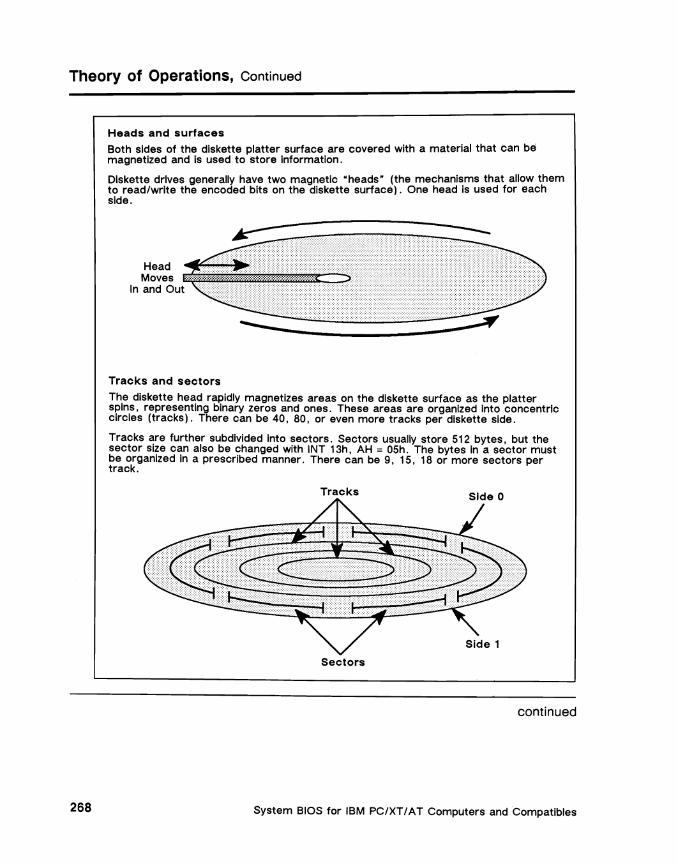
Theory of Operations, Continued
Heads and surfaces Both sides of the diskette platter surface are covered with a material that can be magnetized and Is used to store information.
Diskette drives generally have two magnetic "heads· (the mechanisms that allow them to read/write the encoded bits on the diskette surface). One head is used for each side.
Head Moves
In and Out
Tracks and sectors
The diskette head rapidly magnetizes areas on the diskette surface as the platter spins, representing binary zeros and ones. These areas are organized Into concentric circles (tracks). There can be 40, 80, or even more tracks per diskette side.
Tracks are further subdivided into sectors. Sectors usually store 512 bytes, but the sector size can also be changed with INT 13h, AH = 05h. The bytes In a sector must be organized in a prescribed manner. There can be 9, 15, 18 or more sectors per track.
Tracks Side 0
Sectors
continued
System BIOS for IBM PC/XT/AT Computers and Compatibles 268

Theory of Operations, Continued
How the diskette service works
The BIOS Diskette Service Read, Write, Verify, and Format functions all require data to be transferred to or from the diskette drive to system memory. This is always done using the DMA controller. DMA facilitates the movement of data directly from memory to I/O devices, freeing the microprocessor for other functions. The DMA controller is programmed by the BIOS before the command block is written to the diskette controller. All diskette operations use DMA controller channel 2.
The process of checking the diskette controller status, sending a byte, and waiting is repeated until all bytes in the command block are sent. Once the command block is received, the controller performs the function requested.
After the diskette controller has performed the command and transferred data, an interrupt is generated by the diskette controller. INT OEh, the diskette ISR, handles the interrupt, setting bit 7 of location 40:3Eh. INT 40, the diskette DSR, monitors location 40:3Eh for up to one second, waiting for the interrupt.
The interrupt indicates that one or more (a maximum of 7) result bytes may be waiting for INT 40h to read. If there is no interrupt, the time-out bit in 40:41h is set by INT 40h.
INT 13h Diskette Service 269

Hardware Environment
Hardware assumed
The NEG 765 diskette controller chip (or its equivalent) and some additional logic is used to control the diskette drives.
Diskette change line
Some diskette drives and diskette controllers support a change line signal that is set if the drive door of the selected drive is opened. The caller can use this signal to determine if the sector images in memory are still current. The BIOS checks the change line signal before each diskette I/O operation. Bit 7 of port 03F7h indicates the change line signal status: if not set, the drive door has not been opened and a diskette is probably in the drive. If set, the drive door has been opened and additional verification must take place to determine if the diskette has been changed.
Recalibrating a diskette drive
The following information is provided for programs that bypass BIOS diskette operations and write directly to the diskette hardware.
The diskette status information at location 40:3Eh contains a bit for each diskette drive that indicates if a drive should be recalibrated. The BIOS automatically instructs the diskette controller to recalibrate a drive, if necessary.
How diskette drives are identified
Each diskette drive must be identified to the system with a unique number. There are four valid diskette numbers in an XT system. AT systems support a maximum of two internal drives, and, with an external diskette driver (usually a DOS routine) and a Phoenix BIOS, may support a total of four diskette drives.
• Diskette drive 1 is number 0
• Diskette drive 2 is number 1
• Diskette drive 3 is number 2
• Diskette drive 4 is number 3
These values must be in DL for most Diskette Service functions.
continued
System BIOS for IBM PC/XT/ AT Computers and Compatibles 270
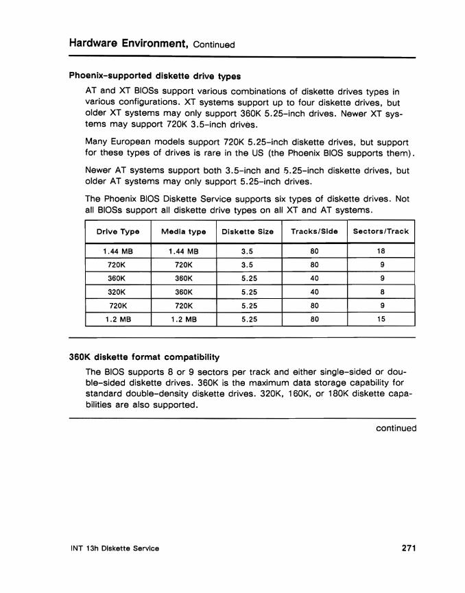
Hardware Environment, Continued
Phoenix-supported diskette drive types
AT and XT BlOSs support various combinations of diskette drives types in various configurations. XT systems support up to four diskette drives, but older XT systems may only support 360K 5.25-inch drives. Newer XT systems may support 720K 3.5-inch drives.
Many European models support 720K 5.25-inch diskette drives, but support for these types of drives is rare in the US (the Phoenix BIOS supports them).
Newer AT systems support both 3.5-inch and !5.25-inch diskette drives, but older AT systems may only support 5.25-inch drives.
The Phoenix BIOS Diskette Service supports six types of diskette drives. Not all BlOSs support all diskette drive types on all XT and AT systems.
Drive Type Media type Diskette Size Tracks/Side Sectors/Track
1.44 MB 1.44 MB 3.5 80 18
720K 720K 3.5 80 9
360K 360K 5.25 40 9
320K 360K 5.25 40 8
720K 720K 5.25 80 9
1.2 MB 1.2 MB 5.25 80 15
360K diskette format compatibility
The BIOS supports 8 or 9 sectors per track and either single-sided or double-sided diskette drives. 360K is the maximum data storage capability for standard double-density diskette drives. 320K, 160K, or 180K diskette capabilities are also supported.
continued
INT 13h Diskette Service 271
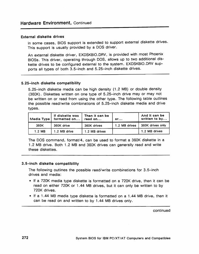
Hardware Environment, Continued
External diskette drives
In some cases, BIOS support is extended to support external diskette drives. This support is usually provided by a DOS driver.
An external diskette driver, EXDSKBIO. DRV, is provided with most Phoenix BlOSs. This driver, operating through DOS, allows up to two additional diskette drives to be configured external to the system. EXDSKBIO.DRV supports all types of both 3.5-inch and 5.25-inch diskette drives.
5.25-inch diskette compatibility
5.25-inch diskette media can be high density (1.2 MB) or double density (360K). Diskettes written on one type of 5.25-inch drive mayor may not be written on or read from using the other type. The following table outlines the possible read/write combinations of 5.25-inch diskette media and drive types.
If diskette was Then It can be And it can be Media Type formatted on ... read on •.. or... written to by ...
360K 360K drive 360K drives 1.2 MB drives 360K drives only
1.2 MB 1.2 MB drive 1.2 MB drives 1.2 MB drives
The DOS command, format/4, can be used to format a 360K diskette in a 1 .2 MB drive. Both 1.2MB and 360K drives can generally read and write these diskettes.
3.5-inch diskette compatibility
The following outlines the possible read/write combinations for 3.5-inch drives and media:
• If a 720K media type diskette is formatted on a 720K drive, then it can be read on either 720K or 1.44 MB drives, but it can only be written to by 720K drives.
• If a 1.44 MB media type diskette is formatted on a 1.44 MB drive, then it can be read on and written to by 1.44 MB drives only.
continued
System BIOS for IBM PC/XT/AT Computers and Compatibles 272

Hardware Environment, Continued
Data transfer rates
All supported formats use a 512-byte sector size. Data transfer rates are:
Transfer Rate Diskette Capacity
250 Kbs
250 Kbs
500 Kbs
300 Kbs
250 Kbs
500 Kbs
Kbs =
360K
720K
1.2 MB
360K
720K
1.44 MB
Kilobits per second
Drive Capacity Drive Size
360K 5.25
720K 3.5
1.2 MB 5.25
1.2 MB 5.25
1.44 MB 3.5
1.44 MB 3.5
INT 13h Diskette Service 273
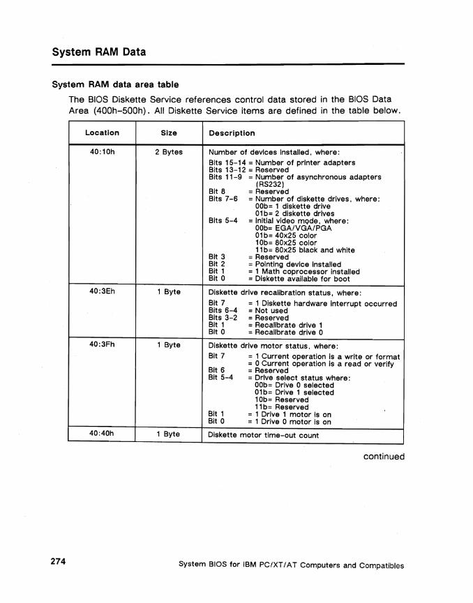
System RAM Data
System RAM data area table
The BIOS Diskette Service references control data stored in the BIOS Data Area (400h-500h). All Diskette Service items are defined in the table below.
Location Size
40:10h 2 Bytes
40:3Eh 1 Byte
40:3Fh 1 Byte
40:40h 1 Byte
Description
Number of devices Installed, where: Bits 15-14 = Number of printer adapters Bits 13-12 = Reserved Bits 11-9
Bit 8 Bits 7-6
Bits 5-4
Bit 3 Bit 2 Bit 1 Bit 0
= Number of asynchronous adapters (RS232)
= Reserved = Number of diskette drives, where:
OOb= 1 diskette drive 01 b= 2 diskette drives
= Initial video mQde, where: OOb= EGAIVGA/PGA 01 b= 40x25 color 10b= 80x25 color 11 b= 80x25 black and white
= Reserved = POinting device installed = 1 Math coprocessor Instal.led = Diskette available for boot
Diskette drive recalibratlon status, where:
Bit 7 = 1 Diskette hardware interrupt occurred Bits 6-4 = Not used Bits 3-2 = Reserved Bit 1 = Recalibrate drive 1 Bit 0 =Recalibrate drive 0
Diskette drive motor status, where: Bit 7
Bit 6 Bit 5-4
Bit 1 Bit 0
= 1 Current operation Is a write or format = 0 Current operation Is a read or verify = Reserved = Drive select status where:
OOb= Drive 0 selected 01b= Drive 1 selected 10b= Reserved 11 b= Reserved
= 1 Drive 1 motor Is on = 1 Drive 0 motor is on
Diskette motor time-out count
continued
System BIOS for IBM PC/XT I AT Computers and Compatibles 274
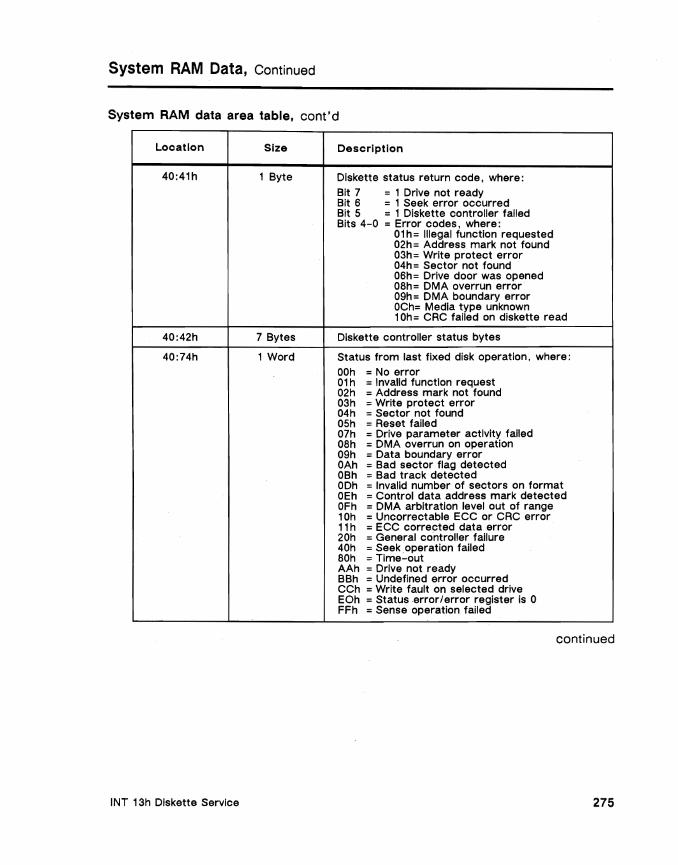
System RAM Data, Continued
System RAM data area table, cont'd
Location Size
40:41h 1 Byte
40:42h 7 Bytes
40:74h 1 Word
Description
Diskette status return code, where: Bit 7 Bit S Bit S Bits 4-0
= 1 Drive not ready = 1 Seek error occurred = 1 Diskette controller failed = Error codes, where:
01 h= Illegal function requested 02h= Address mark not found 03h= Write protect error 04h= Sector not found OSh= Drive door was opened 08h= DMA overrun error 09h= DMA boundary error OCh= Media type unknown 10h= CRC failed on diskette read
Diskette controller status bytes
Status from last fixed disk operation, where: OOh = No error 01h = Invalid function request 02h = Address mark not found 03h = Write protect error 04h = Sector not found OSh = Reset failed 07h = Drive parameter activity failed 08h = DMA overrun on operation 09h = Data boundary error OAh = Bad sector flag detected OBh = Bad track detected ODh = Invalid number of sectors on format OEh = Control data address mark detected OFh = DMA arbitration level out of range 10h = Uncorrectable ECC or CRC error 11 h = ECC corrected data error 20h = General controller failure 40h = Seekoperation failed 80h = Time-out AAh = Drive not ready BBh = Undefined error occurred CCh =Write fault on selected drive EOh = Status error/error register is 0 FFh =Sense operation failed
continued
INT 13h Diskette Service 275
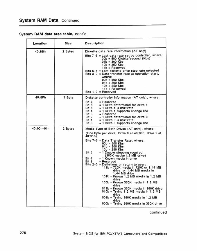
System RAM Data, Continued
System RAM data area table, cont'd
Location Size Description
40:8Bh 2 Bytes Diskette data rate Information (AT only)
Bits 7-6 =Last data rate set by controller, where: OOb = 500 Kilobits/second (Kbs) 01b = 300 Kbs 10b =250 Kbs 11 b =Reserved
Bits 5-4 =Last diskette drive step rate selected Bits 3-2 =Data transfer rate at operation start,
where: OOb =500 Kbs 01b =300 Kbs 10b =250 Kbs 11 b =Reserved
Bits 1-0 = Reserved
40:8Fh 1 Byte Diskette controller information (AT only), where: Bit 7 = Reserved Bit 6 = 1 Drive determined for drive 1 Bit 5 = 1 Drive 1 is multirate Bit 4 = 1 Drive 1 supports change line Bit 3 = Reserved Bit 2 = 1 Di"ive determined for drive 0 Bit 1 = 1 Drive 0 is multirate Bit 0 =1 Drive 0 supports change line
40:90h-91h 2 Bytes Media Type of Both Drives (AT only), where: (One byte per drive. Drive 0 at 40: 90h; drive 1 at 40:91h) Bits 7-6 =Data Transfer Rate, where:
OOb =500 Kbs 01b =300 Kbs 10b =250 Kbs
Bit 5 =1 Double stepping required (360K media/1.2 MB drive)
Bit 4 = 1 Known media In drive Bit 3 = Reserved Bits 2-0 = Definitions on return to user:
11 i b =720K media in 720K or 1 .44 MB drive; or 1.44 MB media in 1.44 MB drive
101b = Known 1.2 MB media in 1.2 MB drive
100b = Known 360K media in 1.2MB drive
011b = Known 360K media in 360K drive 010b = Trying 1.2 MB media in 1.2 MB
drive 001b =Trying 360K media in 1.2 MB
drive OOOb = Trying 360K media In 360K drive
continued
System BIOS for IBM PC/XT/AT Computers and Compatibles 276
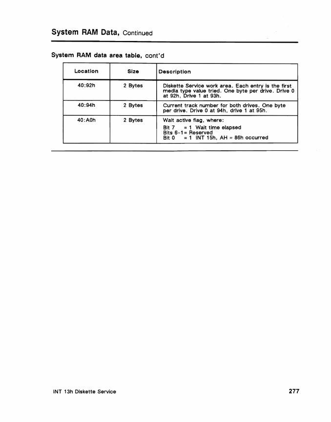
System RAM Data, Continued
System RAM data area table, cont'd
Location Size Description
40:92h 2 Bytes Diskette Service work area. Each entry is the first media type value tried. One byte per drive. Drive 0 at 92h, Drive 1 at 93h.
40:94h 2 Bytes Current track number for both drives. One byte per drive. Drive 0 at 94h, drive 1 at 95h.
40:AOh 2 Bytes Wait active flag, where:
Bit 7 = 1 Wait time elapsed Bits 6-1 = Reserved Bit 0 = 1 INT 15h, AH = a6h occurred
INT 13h Diskette Service 277

CMOS RAM Data
Introduction
The Diskette Service routine makes use of control information located in CMOS RAM data areas OEh through 10h. The table below provides detailed information about the areas used.
CMOS RAM data area table
The following table descrities all CMOS RAM data areas used by this interrupt.
CMOS RAM Offset Size Description
OEh 1 Byte Diagnostic status, where: Bit 7 =1 Real time clock lost power Bit 6 =1 CMOS RAM checksum is bad Bit 5 =1 Invalid configuration information at POST Bit 4 =1 Memory size compare error at POST Bit 3 =1 Fixed disk or adapter fails initialization Bit 2 =1 RTC time found invalid Bit 1 =1 Adapters do not match configuration Bit 0 =1 Time-out in reading an adapter ID
10h 1 Byte Type of diskette drives: Bits 7-4 =Drive type of drive 0, where:
OOOOb =No drive 0001 b =360K drive 0010b =1.2 MB drive 0011b =720K 0100b =1.44 MB
Bits 3-0 =Drive type of drive 1, where: OOOOb =No drive 0001b =360K drive 0010b =1.2 MB drive 0011b =720K 0100b =1.44 MB
System BIOS for IBM PCIXT/AT Computers and Compatibles 278

ROM BIOS Data
Description
The diskette device service routine in PC/XT / AT systems contains a table of parameters used to manipulate diskette drives. For many newer systems, values have been modified so the table is more suitable for use with 3.5inch diskette drives. Both 3.5-inch and 5.25-inch values are provided below. The default 11-byte table is located in ROM at FOOO: EFC7h and is pointed to by the interrupt 1 Eh vector. This arrangement allows operating systems or application programs to change the INT 1Eh vector to point to a different set of diskette parameters.
Diskette parameter table
Offset Description
OOh First data byte of the diskette Specify command, where:
Setting for Bits 7-4 Drive Typel
Transfer Rate F E D C B A
360K/250 Kbs 1 2 3 4 5 6
Other I 500 Kbs 1 2 3 4 5 6
Other/300 Kbs 1.7 3.3 5 6.7 8.3 10
Other/250 Kbs 2 4 6 8 10 12
Bits 3-0 =Head unload time. Default Is 240 milliseconds (OFh).
01h Second data byte of the diskette Specify command, where:
Bits 7-1 =Head load time. Default Is 01h (4 milliseconds). Bit 0 =Non-DMA mode flag The heads are loaded at the same time as the motor Is started, but the motor delay Is much longer so the head load time delay Is not really needed. The non-DMA mode flag Is always set to zero to Indicate that DMA Is being used.
02h Motor turn-off delay. The amount of time in timer ticks that the diskette device service routine waits before turning off an Inactive diskette drive motor. Timer ticks occur 18.2 times per second and the routine walts about two seconds. The default value for this field Is 25h.
continued
INT 13h Diskette Service 279
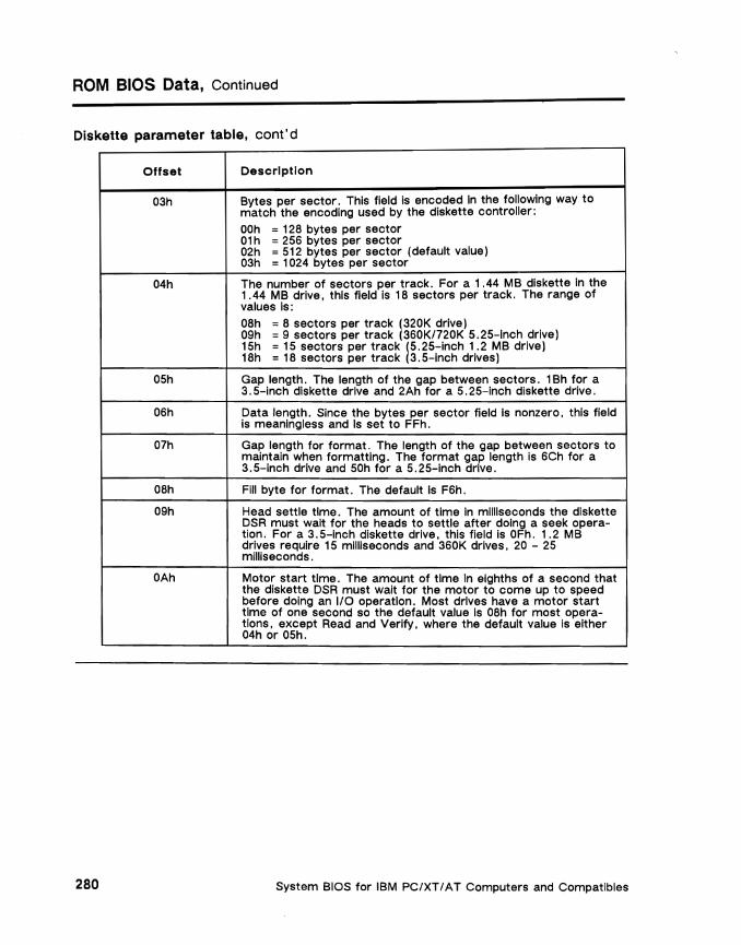
ROM BIOS Data, Continued
Diskette parameter table, cont'd
Offset Description
OSh Bytes per sector. This field is encoded in the following way to match the encoding used by the diskette controller:
OOh =128 bytes per sector 01h =2S6 bytes per sector 02h =S12 bytes per sector (default value) 03h =1024 bytes per sector
04h The number of sectors per track. For a 1.44 MB diskette in the 1.44 MB drive, this field is 18 sectors per track. The range of values Is: 08h =8 sectors per track (320K drive) 09h =9 sectors per track (360K/720K S.2S-lnch drive) 1Sh =15 sectors per track (S.2S-lnch 1.2 MB drive) 18h =18 sectors per track (S.S-Inch drives)
OSh Gap length. The length of the gap between sectors. 1 Bh for a S.5-inch diskette drive and 2Ah for a 5. 25-lnch diskette drive.
06h Data length. Since the bytes per sector field Is nonzero, this field is meaningless and Is set to FFh.
07h Gap length for format. The length of the gap between sectors to maintain when formatting. The format gap length is 6Ch for a 3.S-inch drive and 50h for a S.25-inch drive.
08h Fill byte for format. The default Is F6h.
09h Head settle time. The amount of time In milliseconds the diskette DSR must walt for the heads to settle after doing a seek operation. For a 3. 5-inch diskette drive, this field is OFh. 1.2 M B drives require 15 milliseconds and 360K drives, 20 - 25 milliseconds.
OAh Motor start time. The amount of time In eighths of a second that the diskette DSR must wait for the motor to come up to speed before doing an I/O operation. Most drives have a motor start time of one second so the default value Is 08h for most operations, except Read and Verify, where the default value is either 04h or OSh.
System BIOS for IBM PC/XT/AT Computers and Compatibles 280

Diskette Service I/O Ports
Read/Write Status
R/W
R/W
R/W
W
W
W
R/W
R/W
W
I/O Address
0004h
0005h
OOOAh
OOOBh
OOOCh
0070h
0071h
008111
0372h
Description
DMA channel 2, memory address register
DMA channel 2, transfer count register
DMA channel 0-3, mask register, where:
Bits 7-3 =0 Reserved Bit 2 =0 Clear mask Bit
= 1 Set mask Bit Bits 1-0 =OOb Select channel 0
=01 b Select channell =10b Select channel 2 =11 b Select channel 3
DMA channel 0-3, mode register, where:
DMA Clear Byte Pointer
CMOS RAM address register port, where:
Bit 7 =1 NMI disable =0 NMI enabled
Bits 6-0 = 0 CMOS RAM address
CMOS RAM data register port
DMA channel 2, page register
Diskette controller digital output register, where:
Bits 7-6 =0 Reserved Bit 5 = 1 Enable drive motor 1 Bit 4 =1 Enable drive motor 0 Bit 3 =0 Allow interrupts Bit 2 = 0 Controller reset Bit 1 = 0 Reserved Bit 0 = 0 Select drive 0
=1 Select drive 1
continued
Bits 7-6
Bit 5
Bit 4
Bits 3-2
Bits 1-0
= OOb Demand mode = 01b Signal mode = lOb Block mode =11 b Cascade mode =0 Address Increment select =1 Address decrement select =0 Autoinitialization disable =1 Autoinitialization enable =OOb Verify operation =01 b Write to memory = lOb Read from memory =11 b Reserved =OOb Channel 0 select = 01b Channell select = lOb Channel 2 select =11 b Channel 3 select
INT 13h Diskette Service 281

Diskette Service 110 Ports, Continued
Read/Write 1/0 Address Status Description
0374h R Diskette controller status register, where:
I Bit 7 =1 Data register Is ready Bit 6 =1 Transfer is from controller to
system =0 Transfer is from system to
controller Bit 5 =1 Non-DMA mode Bit 4 =1 Diskette controller busy Bits 3-2 =Reserved Bit 1 =1 Drive 1 busy Bit 0 =0 Drive 0 busy
0375-0376h RIW Diskette controller data registers
0377h R Diskette controller digital input register where:
Bit 7 =Diskette change Bits 6-1 =Reserved Bit 0 =0 High density select
03FOh R Diskette controller status register A, where:
Bit 7 =1 Interrupt pending Bit 6 =0 Second drive installed Bit 5 =1 Step Bit 4 =1 Track 0 Bit 3 =1 Head 1 select Bit 2 =0 Index Bit 1 =0 Write protect Bit 0 =1 Direction
03F1h R Diskette controller status register B, where: Bit 7 =0 Reserved Bit 6 =0 Reserved Bit 5 =0 Select drive 0 Bit 4 =Write data Bit 3 =Read data Bit 2 =1 Write enable Bit 1 =1 Enable drive motor 1 Bit 0 =1 Enable drive motor 0
03F2h W Diskette controller digital output register, where: Bit 7 =0 Reserved Bit 6 =0 Reserved Bit 5 =1 Enable drive 1 motor Bit 4 =1 Enable drive 0 motor Bit 3 DMA
=0 Enable diskette Interrupts and
Bit 2 =0 Controller reset Bit 1 =0 Reserved Bit 0 =0 Select drive 0
=1 Select drive 1
continued
System BIOS for IBM PC/XTIAT Computers and Compatibles 282
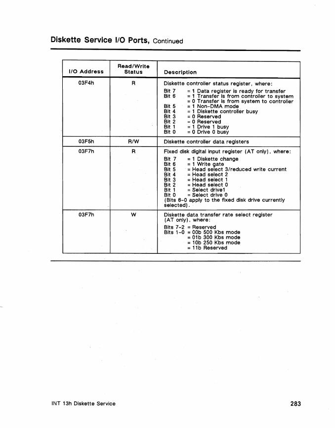
Diskette Service 1/0 Ports, Continued
Read/Write I/O Address Status Description
03F4h R Diskette controller status register. where: Bit 7 Bit 6
=1 Data register is ready for transfer =1 Transfer Is from controller to system
Bit 5 =0 Transfer is from system to controller =1 Non-DMA mode
Bit 4 Bit 3
=1 Diskette controller busy =0 Reserved
Bit 2 =0 Reserved Bit 1 =1 Drive 1 busy Bit 0 =0 Drive 0 busy
03F5h R/W Diskette controller data registers
03F7h R Fixed disk digital input register (AT only), where:
Bit 7 Bit 6 Bit 5
=1 Diskette change =1 Write gate =Head select 3/reduced write current
Bit 4 =Head select 2 Bit 3 =Head select 1 Bit 2 =Head select 0 Bit 1 =Select drlve1 Bit 0 =Select drive 0 (Bits 6-0 apply to the fixed disk drive currently selected) .
03F7h W Diskette data transfer rate select register (AT only), where: Bits 7-2 =Reserved Bits 1-0 =OOb 500 Kbs mode
=01 b 300 Kbs mode =10b 250 Kbs mode = 11 b Reserved
INT 13h Diskette Service 283

Error Handling
Introduction
The BIOS Diskette Service returns the completion status of each function via the AH register. the Carry Flag. and the Diskette Status data definition. located at 40:41h.
Result bytes
The BIOS stores all result bytes returned by the diskette controller in the seven-byte location starting at 40:42h. Usually there are four to seven result bytes.
Successful functions
Successful functions return as follows:
• AH = OOh (No error)
• Diskette Status (40:41 h) = AH
• Carry Flag = 0 (cleared)
Unsuccessful functions
Unsuccessful functions return as follows:
• AH = xxh (an error code - see the following page)
• Diskette Status (40:41 h) = Error code
• Carry Flag = 1 (set)
continued
System BIOS for IBM PC/XT/AT Computers and Compatibles 284
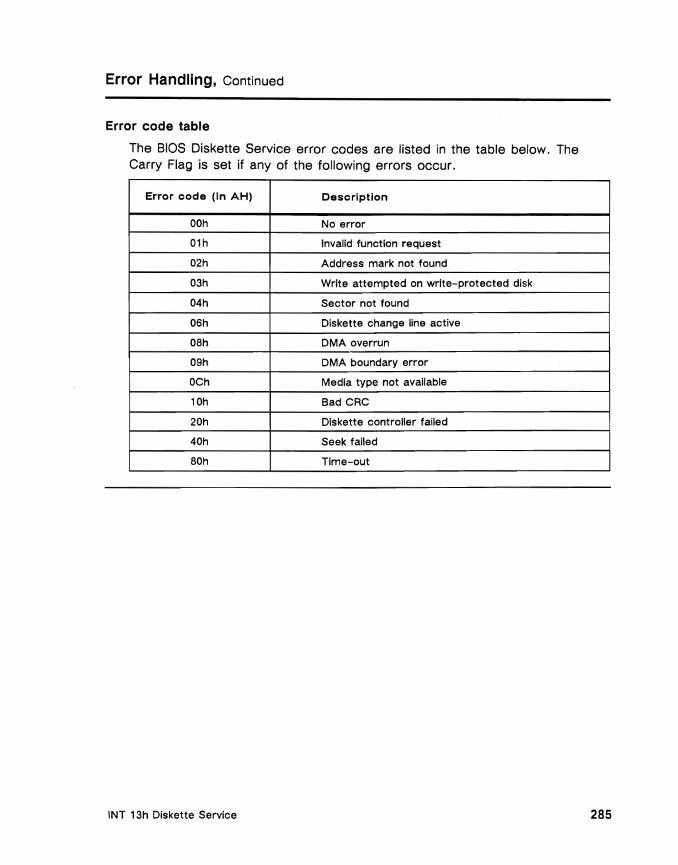
Error Handling, Continued
Error code table
The BIOS Diskette Service error codes are listed in the table below. The Carry Flag is set if any of the following errors occur.
Error code (In AH)
OOh
01h
02h
03h
04h
06h
OBh
09h
OCh
10h
20h
40h
BOh
Description
No error
Invalid function request
Address mark not found
Write attempted on write-protected disk
Sector not found
Diskette change line active
DMA overrun
DMA boundary error
Media type not available
Bad CRC
Diskette controller failed
Seek failed
Time-out
INT 13h Diskette Service 285

Function: AH = OOh Reset Diskette System [XT] [AT]
Description
This function resets both the diskette controller and the specified diskette drive (the R/W arm is moved to track 0). The diskette drive number (either OOh or 01 h) is specified in DL.
Function failure
Call this function when a problem occurs in attempting to access the diskette subsystem with any other function, then retry the function that failed. The diskette subsystem will not react immediately. Instead, a reset flag forces the BIOS to recalibrate the diskette drive's read/write heads the next time they are used. The heads are relocated to track 0 in order to start the next 110 operation from a known state.
Input/Output
Input: AH = OOh DL = Drive number
Bit 7 = o for a diskette 1 for a fixed disk
Output: AH = OOh No error xxh Error (See error code table earlier in this chapter)
= Diskette Status (40:41 h) CF = o No error
= 1 Error
System BIOS for IBM PC/XTIAT Computers and Compatibles 286

Function: AH = 01h Read Diskette Status [XT] [AT]
Description
The BIOS Diskette Service stores the error code associated with the last requested function in Diskette Status (40:41 h). If the last function executed successfully, the Diskette Status and AH are set to OOh. If the last function was not successful, AH and the Diskette Status are set to the appropriate nonzero error code.
This function reads the value contained in Diskette Status and returns it in the AH register. CF is not set by this function.
Input/Output
Input: AH = 01h DL = OOh or 01 h (drive number)
Output: AH OOh No error AL = Diskette Status from previous operation
Diskette status byte
The Diskette Status byte is saved after each read, write, verify or format diskette function. This allows error handling or error reporting routines to be written which are entirely independent of diskette operation routines.
INT 13h Diskette Service 287
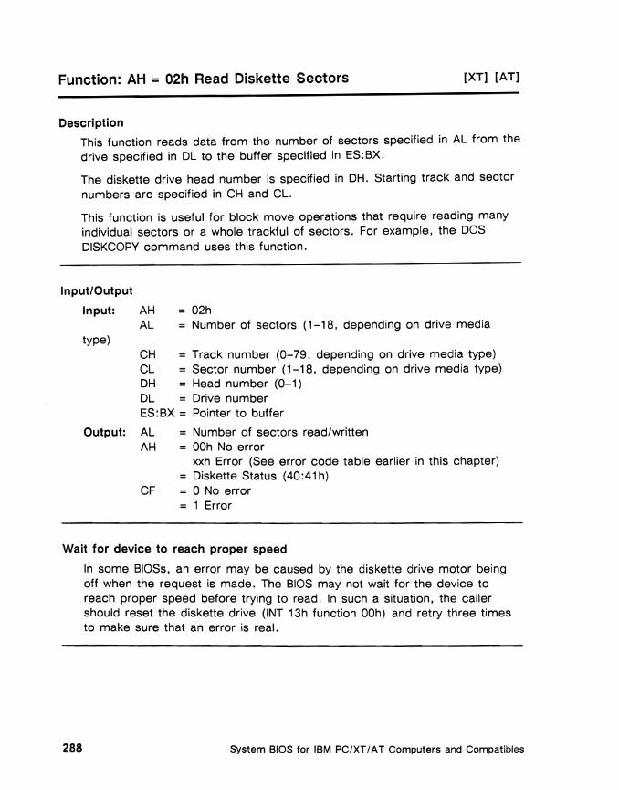
[XT] [AT]Function: AH = 02h Read Diskette Sectors
Description
This function reads data from the number of sectors specified in AL from the drive specified in DL to the buffer specified in ES:BX.
The diskette drive head number is specified in DH. Starting track and sector numbers are specified in CH and CL.
This function is useful for block move operations that require reading many individual sectors or a whole trackful of sectors. For example, the DOS DISKCOPY command uses this function.
Input/Output
Input: AH = 02h AL = Number of sectors (1-18, depending on drive media
type) CH = Track number (0-79, depending on drive media type) CL = Sector number (1-18, depending on drive media type) DH = Head number (0-1) DL Drive number ES:BX = Pointer to buffer
Output: AL Number of sectors read/written AH = DOh No error
xxh Error (See error code table earlier in this chapter) = Diskette Status (40:41 h)
CF = 0 No error = 1 Error
Wait for device to reach proper speed
In some BlOSs, an error may be caused by the diskette drive motor being off when the request is made. The BIOS may not wait for the device to reach proper speed before trying to read. In such a situation, the caller should reset the diskette drive (INT 13h function DOh) and retry three times to make sure that an error is real.
System BIOS for IBM PC/XT/ A T Computers and Compatibles 288

Function: AH = 03h Write Diskette Sectors [XT] [AT]
Description
This function writes data to the number of sectors specified in AL on the drive specified in DL from the buffer specified in ES:BX.
The diskette drive head number is specified in DH. Starting track and sector numbers are specified in CH and CL. Diskette sectors must be formatted before they can be written to.
Input/Output
Input: AH = 03h AL = Number of sectors (1-18, depending on drive media
type) CH = Track number (0-79, depending on drive media type) CL = Sector number (1-18, depending on drive media type) DH = Head number (0-1) DL Drive number ES:BX = Pointer to buffer
Output: AL = Number of sectors read/written AH = OOh No error
xxh Error (See error code table earlier in this chapter) = Diskette Status (40:41 h)
CF = 0 No error = 1 Error
Wait for device to reach proper speed
In some BlOSs, an error may be caused by the diskette drive motor being off when the request is made. The BIOS may not wait for the device to reach proper speed before trying to read. In such a situation, the caller should reset the diskette drive (INT 13h function OOh) and retry three times to make sure that an error is real.
I NT 13h Diskette Service 289
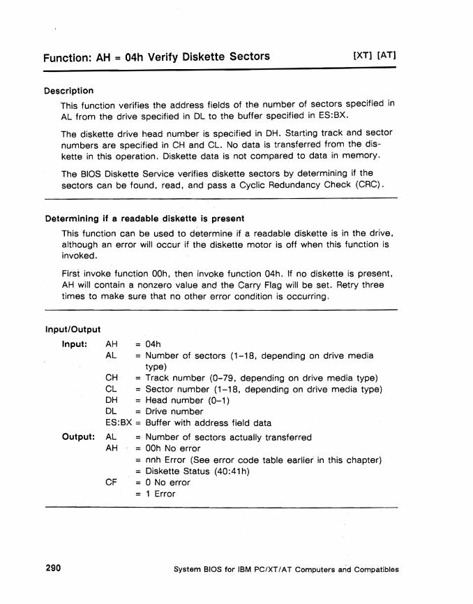
[XT] [AT] Function: AH = 04h Verify Diskette Sectors
Description
This function verifies the address fields of the number of sectors specified in AL from the drive specified in DL to the buffer specified in ES:BX.
The diskette drive head number is specified in DH. Starting track and sector numbers are specified in CH and CL. No data is transferred from the diskette in this operation. Diskette data is not compared to data in memory.
The BIOS Diskette Service verifies diskette sectors by determining if the sectors can be found, read. and pass a Cyclic Redundancy Check (eRC).
Determining if a readable diskette is present
This function can be used to determine if a readable diskette is in the drive. although an error will occur if the diskette motor is off when this function is invoked.
First invoke function OOh. then invoke function 04h. If no diskette is present, AH will contain a nonzero value and the Carry Flag will be set. Retry three times to make sure that no other error condition is occurring.
InputlOutput
Input: AH = 04h AL = Number of sectors (1-18. depending on drive media
type) CH = Track number (0-79. depending on drive media type) CL = Sector number (1-18. depending on drive media type) DH Head number (0-1) DL = Drive number ES:BX = Buffer with address field data
Output: AL = Number of sectors actually transferred AH = OOh No error
= nnh Error (See error code table earlier in this chapter) Diskette Status (40:41h)
CF = 0 No error = 1 Error
System BIOS for IBM PC/XT / AT Computers and Compatibles 290

Function: AH = OSh Format Diskette Track [XT] [AT]
Description
This function formats a single diskette track on the drive specified in DL. The format operation consists of writing the diskette sector and track address field data on the specified track. The number of sectors is specified in AL, the head number in DH, and the track number in CH. Each call to 'function 05h of the Diskette Service, can be verified by following it with a call to function 04h.
ES: BX points to a table defining the address fields for the track being formatted.
If the diskette drive in question supports more than one diskette format, the caller must invoke either Diskette Service Function AH = 17h Set Diskette Type or AH = 18h Set Media Type for Format before calling this function.
Use function 17h first if AT system
. On an AT-compatible system, invoke INT 13h function 17h to select the type of media to be formatted before invoking function 05h.
Input/Output
Input: AH = 05h AL = Number of sectors to be formatted (starts at one) DH = Head number DL = Drive number CH = Track number (starts at 0) ES: BX = Address field buffer
Output: AH = OOh No error = 80h Specified diskette drive does not exist = xxh Error (See error code table earlier in this chapter)
Diskette Status (40:41 h) CF = 0 No error
= 1 Error
continued
INT 13h Diskette Service 291
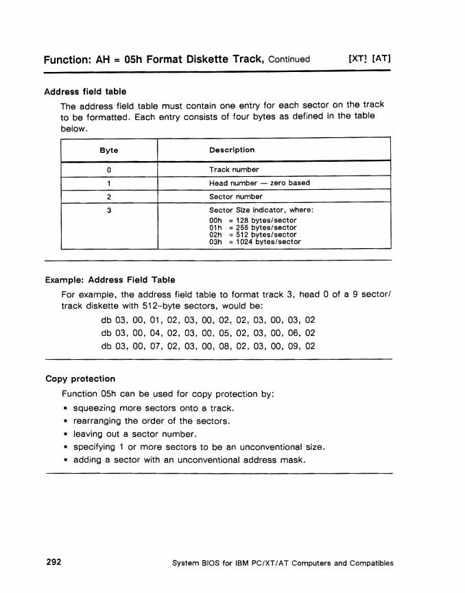
Function: AH = OSh Format Diskette Track, Continued [XT} [AT]
Address field table
The address field table must contain one entry for each sector on the track to be formatted. Each entry consists of four bytes as defined in the table below.
Byte Description
0 Track number
1 Head number - zero based
2 Sector number
3 Sector Size indicator, where: OOh = 128 bytes/sector 01h = 256 bytes/sector 02h = 512 bytes/sector 03h =1024 bytes/sector
Example: Address Field Table
For example, the address field table to format track 3, head 0 of a 9 sectorl track diskette with 512-byte sectors, would be:
db 03, 00, 01, 02, 03, 00, 02, 02, 03, 00, 03, 02
db 03, 00, 04, 02, 03, 00, OS, 02, 03, 00, 06, 02
db 03, 00, 07, 02, 03, 00, 08, 02, 03, 00, 09, 02
Copy protection
Function 05h can be used for copy protection by:
• squeezing more sectors onto a track.
• rearranging the order of the sectors.
• leaving out a sector number.
• specifying 1 or more sectors to be an unconventional size.
• adding a sector with an unconventional address mask.
System BIOS for IBM PC/XT / A T Computers and Compatibles 292
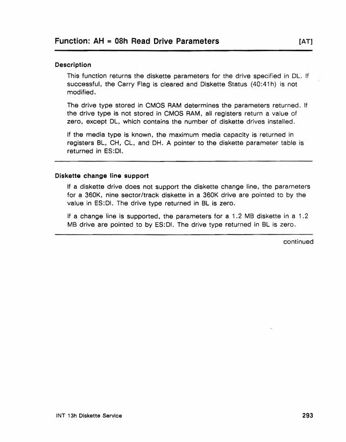
Function: AH = 08h Read Drive Parameters [AT]
Description
This function returns the diskette parameters for the drive specified in Dl. If successful, the Carry Flag is cleared and Diskette Status (40:41 h) is not modified.
The drive type stored in CMOS RAM determines the parameters returned. If the drive type is not stored in CMOS RAM, all registers return a value of zero, except Dl, which contains the number of diskette drives installed.
If the media type is known, the maximum media capacity is returned in registers Bl, CH, Cl, and DH. A pointer to the diskette parameter table is returned in ES:DI.
Diskette change line support
If a diskette drive does not support the diskette change line, the parameters for a 360K, nine sector/track diskette in a 360K drive are pointed to by the value in ES:DI. The drive type returned in BL is zero.
If a change line is supported, the parameters for a 1.2MB diskette in a 1.2 MB drive are pointed to by ES:DI. The drive type returned in BL is zero.
continued
INT 13h Diskette Service 293
Function: AH = OSh Read Drive Parameters, Continued [AT]
Input/Output
Input: AH = 08h DL = Drive number
Output: AX = OOOOh BH = OOh BL Bits 4-7 = 0
Bits 0-3 = Valid drive type value from CMOS RAM 01h = 5.25", 360K, 40 track 02h = 5.25", 1.2 MB, 80 track 03h = 3.5", 720K, 80 track 04h = 3.5", 1.44 MB, 80 track
CF = 0 No error = 1 Invalid parameter
CH Maximum usable track number CL Maximum usable sector number DH = Maximum usable head number
(always 1 if CMOS RAM value valid) DL Number of diskette drives installed (OOh, 01 h, or 02h) ES:DI = Pointer to diskette drive parameter table for
the maximum media type supported on the specified drive
System BIOS for IBM PC/XTIAT Computers and Compatibles 294

Function: AH = 15h Read Drive Type [AT]
Description
This function returns information about the drive specified in DL.
Unlike most other BIOS Diskette Service functions, the value returned in the AH register by this function is not an error code. Instead, the value returned in AH corresponds to one of the four indicators described in the table below.
AH Value Meaning
OOh No drive instalied
01h Diskette drive that cannot detect media change (360K, 40-track diskette)
02h Diskette drive that can detect media change (1.2 MB, aD-track diskette)
03h Fixed disk instalied
Input/Output
Input: AH = 15h DL = Drive number
Output: AH = OOh Drive number is valid 01 h Diskette drive with no change line
= 02h Diskette drive with a change line = 03h Fixed disk installed
CF = o No error 1 Invalid drive number
INT 13h Diskette Service 295
Function: AH = 16h Detect Media Change [AT]
Description
This function determines if the drive door has been opened since the last time the change line was cleared. The change line signal is generally associated with 3.5-inch diskette drives.
If the drive number is not valid, the Carry Flag is set, AH is set to 01h, and control is returned to the caller.
If the specified diskette drive is not configured, AH and Diskette Status are set to 80h (time-out), CF is set, and control is returned to the caller.
Using this function
Invoke INT 13h function 15h first to determine whether the diskette drive hardware can sense when a diskette is changed. AH will be set to 02h if it can.
Diskette change line support
When this function returns with CF set, it does not necessarily mean that a diskette has been changed. It only means that the diskette drive door has been opened and closed since the last time the change line was cleared.
If the change line is not supported. AH and Diskette Status are set to 06h (media change), CF is cleared, and control is returned to the caller.
Input/Output
Input: AH DL =
16h Drive number
Output: AH = OOh Diskette change line signal not active 01 h Invalid drive number
CF
=
=
06h Either change line not supported or diskette change line signal is active
80h Diskette drive not ready or no drive present Diskette Status (40:41 h) 0 No error
= 1 Error
System BIOS for IBM PC/XT I AT Computers and Compatibles 296
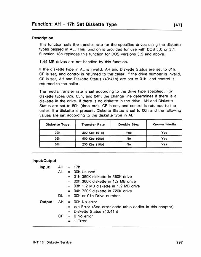
Function: AH = 17h Set Diskette Type [AT]
Description
This function sets the transfer rate for the specified drives using the diskette types passed in AL. This function is provided for use with DOS 3.0 or 3.1. Function 1Bh replaces this function for DOS versions 3.2 and above.
1.44 MB drives are not handled by this function.
If t!1e diskette type in AL is invalid, AH and Diskette Status are set to 01 h, OF is set, and control is returned to the caller. If the drive number is invalid, OF is set, AH and Diskette Status (40:41 h) are set to 01 h, and control is returned to the caller.
The media transfer rate is set according to the drive type specified. For diskette types 02h, 03h, and 04h, the change line determines if there is a piskette in the drive. If there is no diskette in the drive, AH and Diskette Status are set to BOh (time-out), OF is set, and control is returned to the caller. If a diskette is present, Diskette Status is set to OOh and the following values are set according to the diskette type in AL.
Diskette Type Transfer Rate Double Step Known Media
02h 300 Kbs (01b) Yes Yes
03h 500 Kbs (OOb) No Yes
04h 250 Kbs (10b) No Yes
Input/Output
Input: AH = 17h AL ~Oh Unused
01 h 360K diskette in 360K drive = 02h 360K diskette in 1.2MB drive
03h 1.2 MB diskette in 1.2 MB drive = 04h 720K diskette in 720K drive
DL = OOh or 01 h Drive number
Output: AH = OOh No error xxh Error (See error code table earlier in this chapter)
= Diskette Status (40:41 h) OF a No error
1 Error
INT 13h Diskette Service 297
Function: AH = 18h Set Media Type for Format [AT]
Description
This function sets the media type in preparation for a format command.
If the drive number is invalid, the Carry Flag (CF) is set and control is returned to the caller with both AH and Diskette Status (40:41h) = 01h. If the drive type can't be determined, AH and Diskette Status are set to OCh (unknown media), CF is set, and control is returned to the caller.
If there are no problems with the values returned by this function, the BIOS selects a diskette parameter table based on the data input to this function. ES:DI pOints to the chosen diskette parameter table, AH and Diskette Status are set to DOh, CF is cleared, and control is returned to the caller.
Diskette change line support
If the drive number is valid, this function determines if the drive supports a change line. If the drive supports a change line, this function determines if there is a diskette in the drive. If there is no diskette, AH and Diskette Status are set to BOh (time-out), the Carry Flag (CF) is set, and control is returned to the caller.
Using this function
Invoke this function before formatting a diskette with function 05h so the BIOS can set the correct data rate for the media.
continued
System BIOS for IBM PC/XT/ AT Computers and Compatibles 298
Function: AH = 18h Set Media Type for Format, Continued [AT]
Input/Output
Input: AH = 18h CH Maximum number of tracks CL = Maximum sectors per track DL Drive number
Output: ES:DI Pointer to drive parameter table AH DOh track/sector combination is supported
OCh Media unknown (CMOS RAM not valid, drive not configured in CMOS RAM, or not in the diskette parameter table)
80h No diskette in drive Diskette Status (40:41 h)
CF = o No error 1 Error
INT 13h Diskette Service 299

INT OEh Diskette Hardware Interrupt
Introduction
The BIOS Diskette Interrupt Service Routine (ISR) services interrupts from the diskette controller.
How BIOS Diskette ISR is invoked
The diskette controller generates an INT OEh, the BIOS Diskette ISR, to signal the completion of the last command issued by INT 13h.
The INT OEh entry point is located at address FOOO:EF57h. INT OEh resides at address 38h in the interrupt vector table.
BIOS multitasking support
Each time the BIOS Diskette Service issues a diskette controller command, it also invokes INT 15h with AH = 90h Device Busy Loop.
Calling INT 15h allows other tasks in the system to process while diskette 1/0 is in progress. However, this multitasking must be implemented by usersupplied programs executing in the microprocessor's real address mode.
INT OEh and multitasking return
When the diskette controller completes a command, it issues an INT OEh interrupt and enables interrupts.
INT OEh sets bit 7 of the diskette drive recalibrate status byte (40:3Eh,) and calls INT 15h with AH = 91 hand AL = 01 h Interrupt Complete. It then sets bit 7 of (40:3Eh) to signal the completion of the command.
continued
System BIOS for IBM PC/XT/AT Computers and Compatibles 300

INT OEh Diskette Hardware Interrupt, Continued
System RAM data area
INT OEh, Diskette ISR, references the following system RAM data area location:
Location Length Description
3Eh 1 Byte Diskette drive recalibrate status, where: Bit 7 = 1 Diskette hardware Interrupt has
occurred Bit 6-4 = Not used Bits 3,2 = Reserved Bit 1 = 1 Recalibrate drive 1 Bit 0 = 1 Recalibrate drive 0
I/O Port table
INT OEh, Diskette ISR, references the following 1/0 port:
ReadlWrite 1/0 Address Status
03FOh R
Description
Diskette controller status register A, where: Bit 7 = 1 Interrupt pending Bit 6 = 0 Second drive installed Bit 5 = 1 Step Bit 4 = 0 Track 0 Bit 3 = 1 Select head 1 Bit 2 = 0 Index Bit 1 = 0 Write protect Bit 0 = 1 Direction Is from controller to diskette
INT 13h Diskette Service 301

Chapter 11
INT 13h Fixed Disk Service
Overview
Description
The BIOS Fixed Disk Service performs read, write, format, diagnostic, initialization and other operations for up to two fixed disk drives.
How the service is invoked
INT 13h invokes the BIOS Diskette and Fixed Disk Service. If a fixed disk drive is present, the Fixed Disk Service redirects the INT 13h vector to the interrupt vector table address 00:4Ch. The Phoenix AT and XT BlOSs initialize the INT 13h Fixed Disk Service vector to FOOO:E3FEh.
BIOS diskette support
When a fixed disk is installed, the BIOS automatically redirects all INT 13h Diskette Service requests to INT 40h. This redirecting is transparent to end users. End users should continue to invoke INT 13h for both diskette and fixed disk services.
For a discussion of the BIOS Diskette Services, refer to Chapter 10.
continued
INT 13h Fixed Disk Service 303

Overview, Continued
In this chapter
This chapter focuses on the BIOS Fixed Disk Service. The following topics are presented:
• Fixed Disk Service Function Summary
• Theory of Operations
• Hardware Environment
• System RAM Data
• CMOS RAM Data
• ROM BIOS Data
• Fixed Disk Service I/O Ports
• Error Handling
• Fixed Disk Service Functions
How to determine level of support
Throughout this book, the commonly accepted level of support for each ROM BIOS function is identified by the legend [PC], [XT] , and/or [AT] on the same line as the function title. In this chapter, the designation [XT] refers to XT-type fixed disk controller support. [AT] refers to AT-type fixed disk controller support.
Legend Description
[PC] Function Is supported by original IBM PC BIOS only.
[XT] Function Is supported by all IBM PC/XT and compatible ROM BlOSs.
Note: This level of support Is contained In the ROM BIOS implemented In the majority of IBM PC and PC/XT compat-Ible systems.
[AT] Function is supported by all IBM PCIA T and compatible ROM BlOSs.
System BIOS for IBM PC/XTIA T Computers and Compatibles 304

Fixed Disk Service Function Summary
Summary of fixed disk service functions
The BIOS Fixed Disk Service contains twenty-three functions. Individual functions are selected via AH. The table below summarizes these functions. The notation in the Controller Type column refers specifically to the type of fixed disk controller in the system, not necessarily the type of system.
Function
OOh
01h
02h
03h
04h
OSh
OSh
07h
08h
09h
OAh
OBh
OCh
ODh
OEh
OFh
10h
11 h
12h
13h
14h
1Sh
Description
Reset Diskette(s) and Fixed Disk
Read Fixed Disk Status
Read Sectors
Write Sectors
Verify Sectors
Format Cylinder
Format Bad Track
Format Drive
Read Drive Parameters
Initialize Drive Parameters
Read Long Sectors
Write Long Sectors
Seek to Cylinder
Alternate Fixed Disk Reset
Diagnostics 1: Read Test Buffer
Diagnostics 2: Write Test Buffer
Test for Drive Ready
Recallbrate Drive
Controller RAM Diagnostic
Controller Drive Diagnostic
Controller Internal Diagnostic
Read Fixed Disk Type
Controller type
[XT] [AT]
[XT] [AT]
[XT] [AT]
[XT] [AT]
[XT] [AT]
[XT] [AT]
[XT]
[XT]
[XT] [AT]
[XT] [AT]
[XT] [AT]
[XT] [AT]
[XT] [AT]
[XT] [AT]
[XT]
[XT]
[XT] [AT]
[XT] [AT]
[XT] [AT]
[XT] [AT]
[XT] [AT]
[XT] [AT]
INT 13h Fixed Disk Service 305
Theory of Operations
History
Fixed disks were not supported in the original IBM PC. The IBM XT, introduced later, contained the first fixed disk controller, supporting only one fixed disk drive. XT -type fixed disk controllers are still in use today, even in some AT-compatible systems. Today, most XT-type fixed disk controllers support two or more fixed disk drives.
Although the ST506 interface standard permits support of up to four drives per controller, most AT-type fixed disk controllers support up to two fixed disk drives. Almost all AT BlOSs support a maximum of two fixed disk drives. Most systems have a combination diskette/fixed disk controller.
Fixed disk basics
A fixed disk is an electromechanical device. The electronic part includes the read/write head (s), which are essentially electromagnets that convert rapidly pulsing digital electronic signals from the computer to semi-permanent magnetic fields on a specific location on the disk surface. There are other electronic components that control the mechanical parts. They properly align the magnetic storage and help to locate the information on the disk surface.
The mechanical part of a fixed disk drive includes a spindle (a shaft that connects directly to the disk drive motor), and disk platters (upon which data is actually written). The motor spins the disk platter at a precisely controlled speed. The only other mechanical part is the arm, upon which the read/write heads are mounted. The arm allows the heads to move freely just above the disk surface so that the heads can be placed anywhere between the inner and outermost part of the surface. Fixed disks usually have many read/write heads and both sides of the disk platters are used. There is one read/write heads positioned just above the surface of each side of the disk platter. The graphic on the following page describes these terms.
continued
System BIOS for IBM PC/XT IAT Computers and Compatibles 306
Theory of Operations, Continued
continued
INT 13h FIxed Disk Service 307

Theory of Operations, Continued
Fixed disk drive organization
The following graphic explains fixed disk tracks and sectors.
Heads and surfaces
Fixed disk drives generally have several magnetic "heads" (the mechanisms that allow them to read/write the encoded bits on the fixed disk platter surfaces). One head is used for each side of each disk platter. A fixed disk can have many disk platters.
All sides of the fixed disk platter surfaces are covered with a material that can be magnetized and Is used to store Information.
MovesHead .;~~t±~~~~~ZZt:::3 •••••••••••• n) •••••••• In and Out
Tracks and sectors
The fixed disk head rapidly magnetizes areas on the surface of the disk platter as the platter spins, representing binary zeros and ones. These areas are organized into concentric circles (tracks). There can be 40, 80, or even more tracks per fixed disk side.
Tracks are further subdivided into sectors. Sectors usually store 512 bytes. but the sector size can also be changed with INT 13h. AH = 05h. The bytes in a sector must be organized in a prescribed manner. There can be 17. 26. 34 or more sectors pertrack.
Tracks Side 0
Sectors
continued
System BIOS for IBM PC/XT / AT Computers and Compatibles 308

Theory of Operations, Continued
Fixed disk processing
Like the Diskette Service, the BIOS Fixed Disk Service programs the fixed disk controller directly. The BIOS never writes directly from the processor to the fixed disk drive. Sometimes data and commands are sent directly to the controller from the microprocessor, but more often, the BIOS uses the DMA controller.
The BIOS uses the DMA controller to move data directly to and from system memory without the intervention of the microprocessor.
The fixed disk controller communicates directly between the fixed disk drive, the processor, and system memory. It uses DMA channel 2 to access memory.
The following graphic depicts the relationship between the processor, system memory, the DMA channel, the fixed disk controller, and the fixed disk drive.
System <: DMA Channe'Memory
~ Fixed Disk Controller
f'J ... commanf
Read &' Write oat,!
,
Processor ~Re.u,to
01.. 01
....
Step Control
Fixed Disk Drive
r' ...
Motor' COmmand? Control
Selectio'!.. ~
continued
INT 13h Fixed Disk Service 309

Theory of Operations, Continued
Fixed disk controller interfaces
The computer does not access the fixed disk directly. The computer communicates with the fixed disk controller which controls the fixed disks and often also the diskettes. The fixed disk controller uses a predetermined standard for formatting instructions and data (called an interface) for accessing the fixed disk. There are three widely used fixed disk controller standards (or interfaces) :
• ST506/ST 412 - the standard interface
• ESDI (enhanced small device interface), and
• SCSI (small computer systems interface).
Fixed disk data encoding methods
On the ST506 interface, the disk-generated pulses that are used to represent the actual data are passed directly to the controller and the way these pulses are arranged can make a big difference in fixed disk drive performance.
There are several methods of data encoding used by ST506 fixed disk controllers. The most frequently used methods are:
• MFM - modified frequency modulation,
• RLL - run length limited, and
• ARLL - advanced run length limited
Encoding methodologies and the BIOS
The BIOS Fixed Disk Service does not need to worry about different types of encoding or interface methods for fixed disk drives. The BIOS uses the fixed disk drive parameters stored in the fixed disk drive type table in the ROM BIOS data area. See the ROM BIOS Data heading later in this chapter.
continued
System BIOS for IBM PC/XT/AT Computers and Compatibles 310

Theory of Operations, Continued
Fixed disk drive types and the user
XT fixed disk controllers support a limited number of fixed disk drives, so an XT system user has a limited choice of fixed disk drive types. Only four drive types are available. See the ROM BIOS Data heading in this chapter for a description of the XT fixed disk drive types.
In an AT system, the BIOS or computer manufacturer changes the drive types (1-47) and fixed disk parameter table entries to correspond to popular types of fixed disk drives that use the various interfaces and encoding methods. Therefore, many popular types of fixed disk drives that use MFM, RLL, ARLL, or ESDI are available to the end user. The user can access the fixed disk drive type table in the ROM BIOS Data Area and select a fixed disk drive type that corresponds to the parameters of the system's fixed disk drive.
The end user can also use a BIOS utility program, such as the Phoenix SETUP utility, to change the fixed disk drive type table to ensure that the fixed disk drive is supported.
Setting up a fixed disk drive
In systems with XT fixed disk controllers, installing a fixed disk drive requires only physical installation and no software setup.
In AT systems, a SETUP utility must be used. The user needs to know several facts about the fixed disk drive, including the:
• cylinder write precompensation value,
• number of heads,
• number of cylinders,
• number of sectors per track,
• landing zone value, and
• capacity.
The user can look up the fixed disk drive type table stored in the system BIOS (usually the SETUP help facility provides this information) and find the drive type that matches the characteristics of his fixed disk drive.
Some BlOSs provide editable drive types. Phoenix BlOSs provide types 48 and 49, which the user can modify by entering the parameter values of the fixed disk drive with the SETUP utility. The data is automatically stored in CMOS RAM.
INT 13h Fixed Disk Service 311

Hardware Environment
Support for two fixed disk drives
The BIOS Fixed Disk Service supports up to two fixed disk drives. An ST412/506 interface fixed disk controller or equivalent is assumed present. The BIOS uses information from the drive table which may include support for RLL and ESDI drives. ESDI drives generally require an option ROM, which replaces part of the ROM BIOS data.
Older XT -type fixed disk controllers may support only one fixed disk drive. These controllers may be found in both AT and XT systems.
How fixed disks are identified
There are only two valid fixed disk identification numbers - BOh and B1 h. The numbers must be assigned as follows:
• Fixed Disk Drive 0 = 80h
• Fixed Disk Drive 1 = 81 h
Note: The fixed disk drive values BOh or B1 h are required DL register inputs for many of the INT 13h fixed disk services.
BIOS allows processing while disk activity is performed
The BIOS issues an INT 15h, AH = 90h Device Busy (AL = OOh fixed disk) call while waiting for fixed disk interrupts, informing the operating system that the BIOS is waiting for the fixed disk hardware, so processing can go on. When the fixed disk interrupt occurs, the BIOS issues an INT 15h, AH = 91h Interrupt Complete (AL = OOh fixed disk), indicating that the fixed disk operation is complete.
System BIOS for IBM PCfXT f AT Computers and Compatibles 312

System RAM Data
Introduction
The BIOS data area (address 400h - 500h) contains data definitions that are referred to by the BIOS Fixed Disk Service.
Location Size
40:74h 1 Word
40:7Sh 1 Byte
40:76h 1 Byte
40:77h 1 Byte
40:8Ch 1 Byte
40:8Dh 1 Byte
40:8Eh 1 Byte
Description
Status from last fixed disk operation. where: OOh =No error 01h =Invalid function request 02h =Address mark not found 03h =Write protect error 04h =Sector not found OSh =Reset failed 07h =Drive parameter activity failed OSh =DMA overrun on operation 09h =Data boundary error OAh =Bad sector flag detected OBh =Bad track detected ODh = Invalid number of sectors on format OEh =Control data address mark detected OFh =DMA arbitration level out of range 10h =Uncorrectable ECC or CRC error 11 h =ECC corrected data error 20h =General controller failure 40h = Seek operation failed SOh =Time-out AAh =Drive not ready BBh =Undefined error occurred CCh =Write fault on selected drive EOh =Status error/error register Is 0 FFh =Sense operation failed
Number of fixed drives (AT only)
Control byte (when to write to I/O port 03F6h) .
Fixed disk port offset
Fixed disk controller status (AT only)
Fixed disk controller error status (AT only)
Fixed disk interrupt flag (AT only)
INT 13h Fixed Disk Service 313

CMOS RAM Data
Table of CMOS RAM data used
The CMOS RAM data referenced by the Fixed Disk Service is listed below.
CMOS RAM Offset (hex) Size Description
OEh 1 Byte Diagnostic status, where:
Bit 7 = 1 Real time clock lo~~ power Bit 6 =1 CMOS RAM checksum is bad Bit 5 = 1 Invalid configuration information at POST Bit 4 = 1 Memory size compare error at POST Bit 3 = 1 Fixed disk or controller fails initialization Bit 2 = 1 RTC time invalid Bit 1 =1 Controllers do not match configuration Bit 0 = 1 Time-out in reading an controller 10
11 h 1 Byte Type of fixed disk drive 0
12h 1 Byte Type of fixed disk drive 1
19h 1 Byte Drive type of fixed disk 1
1Ah 1 Byte Drive type of fixed disk 2
System BIOS for IBM PC/XT I AT Computers and Compatibles 314

ROM BIOS Data
AT fixed disk parameter table structure
The 16-byte AT fixed disk parameter table defines the types of fixed disk drives that can be used in an AT-compatible system. The address of the correct entry within the fixed disk parameter table is contained in the INT 41 h vector for drive 0 and in the INT 46h vector for drive 1. The INT 41 h fixed disk parameter table is usually located at FOOO:E401 h. The default location of the INT 46h table is often the same as the INT 41 h vector. By invoking INT 13h AH = 08h Read Drive Parameters, the caller can find out where the fixed disk parameter table is located.
Offset Size Description
DOh 2 Bytes Maximum number of cylinders
02h 1 Byte Maximum number of heads
03h 2 Bytes Reserved
OSh 2 Bytes Starting write precompensation cylinder
07h 1 Byte Reserved
08h 1 Byte Control byte. where:
Bit 7 =1 Disable retries Bit 6 =1 Disable retries Bit 5 =1 Defect map present at maximum
cylinder + 1 Bit 4 =0 Reserved Bit 3 =1 More than 8 heads Bits 2-0 =0 Reserved
09h 3 Bytes Reserved
OCh 2 Bytes Landing zone cylinder
OEh 1 Byte Number of sectors per track
OFh 1 Byte Reserved
continued
iNT 13h Fixed Disk Service 315
ROM BIOS Data, Continued
XT fixed disk parameter table structure
The XT fixed disk parameter table defines the types of fixed disk drives that can be used in an XT -compatible system. The address of the correct entry within the fixed disk parameter table is contained in the INT 41 h vector. The fixed disk parameter table is usually located at FOOO:E401 h. By invoking INT 13h, AH = 08h Read Drive Parameters, the caller can find out where the fixed disk parameter table is located.
Offset Size Description
OOh 2 Bytes Maximum number of cylinders
02h 1 Byte Maximum number of heads
03h-04h 2 Bytes Starting reduced write current cylinder
OSh-06h 2 Bytes Starting write precompensation cylinder
07h 1 Byte Maximum ECC burst length
08h 1 Byte Control byte, where: Bit 7 = 1 Disable retries Bit 6 = 1 Disable ECC retries Bits S-3 = 0 Reserved Bits 2-0 = Drive option
09h 2 Bytes Standard timeout value
OAh 1 Byte Timeout value for format drive command
aBh 1 Byte Timeout value for check drive command
aCh 4 Bytes Reserved
continued
System BIOS for IBM PC/XT I A T Computers and Compatibles 316

ROM BIOS Data, Continued
AT fixed disk drive type table
The fixed disk drives that the AT BIOS supports are stored in a ROM-based table. In the Phoenix AT BIOS. table entries 48 and 49 are left for the end user to define by running SETUP. Once specified. the drive characteristics remain stored in CMOS RAM. The end user can add any type of ATcompatible fixed disk drive to a system in this manner. This list is by no means inclusive. but is merely the default drive types provided by Phoenix. Some manufacturers define many more default drive types; others provide means for user definition of drive types.
The Phoenix default drive type table is shown below. We have included the names of many popular fixed disk drive types for easy identification.
# Drive Type Cylinders Heads Write
Precomp Landing
Zone Sectors
1 IBM 5.25" 10 MB 306 4 128 305 17
2 IBM 5.25" 20 MB Seagate ST-225
CDC Wren II 9415-5-25 •
Miniscribe 8438F
615 4 300 615 17
3 IBM 5.25" 30 MB 615 6 300 615 17
4 IBM 5.25" 62 MB 940 8 512 940 17
5 IBM 5.25" 46 MB 940 6 512 940 17
6 IBM 5.25" 20 MB
Miniscribe MS 8425 Tandon TM 262 •••
Tandon TM 702AT •••
615 4 -1 615 17
7 IBM 5.25" 30 MB 462 8 256 511 17
8 IBM 5.25" 30 MB Seagate ST-4038 •••
CDC Wren II 9415-5-38 ••••
Tandon TM 703AT •••
733 5 -1 733 17
9 IBM 5.25" 112 MB
Priam IDEO 130' 900 15 -1 901 17
• The OEM may have to disable drive connector J1 pin 2 when used on the AT ... ... Remove jumper W3 .
Values for Write Precomp of -1, 0, or the last track are assumed to be equivalent.
continued
INT 13h Fixed Disk Service 317

ROM BIOS Data, Continued
AT fixed disk drive type table, cont'd
Write Landing # Drive Type Cylinders Heads Precomp Zone Sectors
10 IBM 5.25" 20 MB 820 3 -1 820 17
Priam IDED75, 100, 120, 150, 160, 230, 330·
11 IBM 5.25" 35 MB 855 5 -1 855 17
Priam IDEO 40, 45, 45H Priam ID45T -5, ID45T-Q.
12 IBM 5.25" 49 MB 855 7 -1 855 17
13 IBM 5.25" 20 MB 306 8 128 319 17
14 IBM 5.25" 42 MB 733 7 -1 733 17
15 Reserved
16 IBM 5.25" 20 MB 612 4 0 663 17
17 IBM 5.25" 40 MB 977 5 300 977 17
18 IBM 5.25" 56 MB 977 7 -1 977 17 Priam ID 60, 62·
19 IBM 5.25" 59MB 1024 7 512 1023 17
20 IBM 5.25" 30 MB 733 5 300 732 17
21 IBM 5.25" 42 MB 733 7 300 732 17
22 IBM 5.25" 30 MB 733 5 300 733 17
23 IBM 5.25" 10 MB 306 4 0 336 17
24 Priam IDEO 62 1024 7 -1 1024 17
25 NEC 5126 20 MB 615 4 0 615 17
26 Micropoiis 1323 ••• 1024 4 -1 1024 17 Rodlme 5040
27 Mlcropolis 1323A _•• 1024 5 -1 1024 17 Seagate ST -4077R Miniscribe 3053/6053
Priam IDEO 45, 45H-·
-_. The OEM may have to disable drive connector J1 pin 2 when used on the AT. Remove jumper W3.
••• Values for Write Precomp of -1, 0, or the last track are assumed to be equivalent.
continued
System BIOS for IBM PC/XT /AT Computers and Compatibles 318
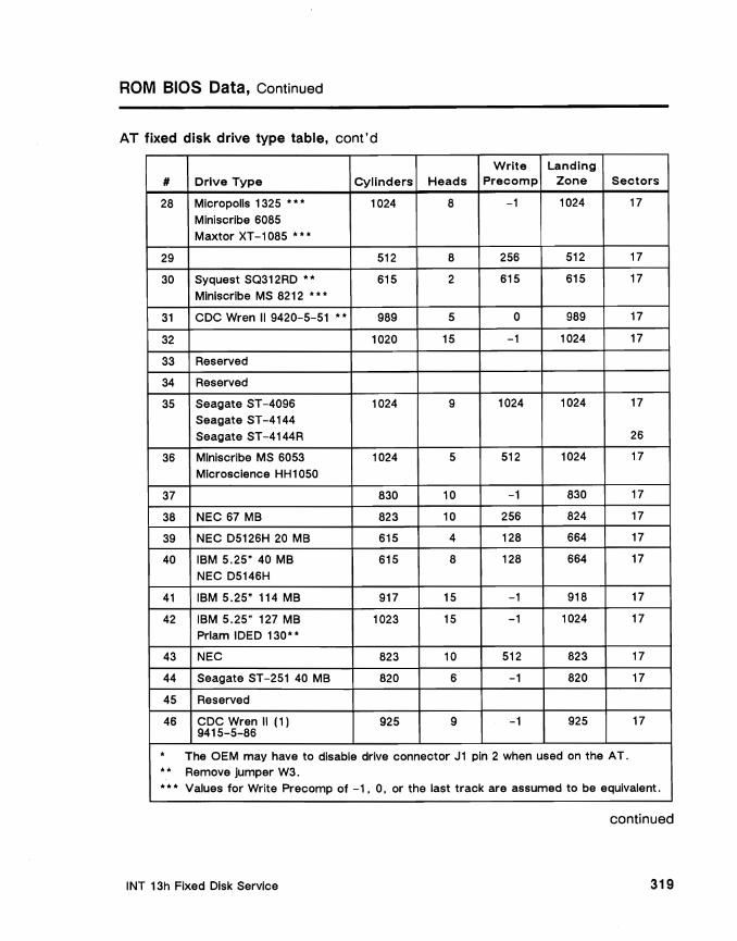
ROM BIOS Data, Continued
AT fixed disk drive type table, cont'd
Write Landing # Drive Type Cylinders Heads Precomp Zone Sectors
28 Micropolis 1 325 ••• 1024 8 -1 1024 17 Mlniscribe 6085 Maxtor XT-1085 •••
29 512 8 256 512 17
30 Syquest SQ312RD .. 615 2 615 615 17 Minlscribe MS 8212 •••
31 CDC Wren II 9420-5-51 •• 989 5 0 989 17
32 1020 15 -1 1024 17
33 Reserved
34 Reserved
35 Seagate ST -4096 1024 9 1024 1024 17 Seagate ST -4144 Seagate ST -4144R 26
36 Mlnlscrlbe MS 6053 1024 5 512 1024 17 Microscience HH1050
37 830 10 -1 830 17
38 NEC 67 MB 823 10 256 824 17
39 NEC D5126H 20 MB 615 4 128 664 17
40 IBM 5.25" 40 MB 615 8 128 664 17 NEC D5146H
41 IBM 5.25" 114 MB 917 15 -1 918 17
42 IBM 5.25" 127 MB 1023 15 -1 1024 17 Priam IDED 130··
43 NEC 823 10 512 823 17
44 Seagate ST -251 40 MB 820 6 -1 820 17
45 Reserved
46 CDC Wren II (1) 925 9 -1 925 17 9415-5-86
• The OEM may have to disable drive connector J 1 pin 2 when used on the AT . •• Remove jumper W3 . ••• Values for Write Precomp of -1. O. or the last track are assumed to be equivalent .
continued
INT 13h Fixed Disk Service 319
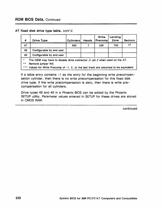
ROM SIOS Data, Continued
AT fixed disk drive type table, cont'd
#
47
Drive Type Cylinders
699
Heads
7
Write Precomp
256
Landing Zone
700
Sectors
17
48 Conflgurable by end user
49 Conflgurable by end user . The OEM may have to disable drive connector J 1 pin 2 when used on the AT . .. ... Remove jumper W3 . Values for Write Precomp of -1, 0, or the last track are assumed to be equivalent .
If a table entry contains -1 as the entry for the beginning write precompensation cylinder, then there is no write precompensation for this fixed disk drive type. If the write precompensation is zero, then there is write precompensation for all cylinders.
Drive types 48 and 49 in a Phoenix BIOS can be edited by the Phoenix SETUP utility. Parameter values entered in SETUP for these drives are stored in CMOS RAM.
continued
System BIOS for IBM PC/XT I A T Computers and Compatibles 320

ROM BIOS Data, Continued
XT fixed disk drive types
Systems with an XT -type fixed disk controller support only four fixed disk drive types. The fixed disk parameter values for each of these XT drive types are defined below. Some AT systems may have XT -type fixed disk controllers.
Parameter Type 0 Type 1 Type 2 Type 3
Maximum cylinders 306 612 615 306
Maximum head(s) 4 4 4 8
Reduced write current cyl. 306 612 615 306
Write precomp cylinder 0 0 300 128
ECC Data Burst Length 11 11 11 11
Control byte 5 5 5 5
Standard time-out 12 32 24 12
Format drive time-out 180 180 180 180
Check drive time-out 40 40 40 40
Reserved 0 0 0 0
Reserved 0 0 0 0
Reserved 0 0 0 0
Reserved 0 0 0 0
INT 13h Fixed Disk Service 321

Fixed Disk Service 1/0 Ports
The INT 13h Fixed Disk Service references the following I/O ports:
Read/Write I/O Address status
0020h R
0020h R
0020 W
Description
Programmable Interrupt Controller - Interrupt request/in-service registers programmed by Operation Command Word 3 (OCW3): Interrupt request register, where: Bits 7-0 =0 No active request for the
corresponding interrupt line =1 Active request for the
corresponding interrupt line
Interrupt in-service register, where: Bits 7-0 =0 The corresponding interrupt line is
not currently being serviced =1 The corresponding Interrupt line Is
currently being serviced
Programmable Interrupt Controller - Initialization Command Word 1 (ICW1) (Bit 4 is one), where: Bits 7-5 =000 Only used in 80/85 mode Bit 4 =1 Reserved Bit 3 =0 Edge triggered mode
=1 Level triggered mode Bit 2 =0 Successive interrupt vectdrs are
separated by eight bytes =1 Successive interrupt vectors are
separated by four bytes Bit 1 =0 Cascade mode
=1 Single mode - no ICW3 needed Bit 0 =0 No ICW4 needed
=1 ICW4 needed
continued
System BIOS for IBM PC/XT / A T Computers and Compatibles 322
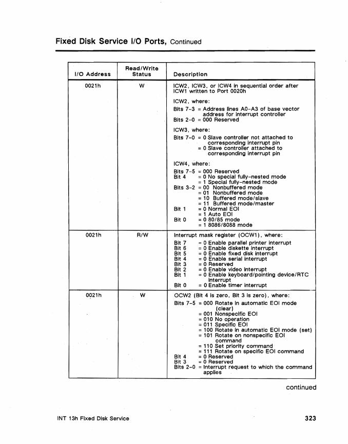
Fixed Disk Service 1/0 Ports, Continued
Read/Write 110 Address Status Description
0021h W ICW2, ICW3, or ICW4 in sequential order after ICWl written to Port 0020h
ICW2, where: Bits 7-3 = Address lines AO-A3 of base vector
address for Interrupt controller Bits 2-0 = 000 Reserved
ICWS, where: Bits 7-0 = 0 Slave controller not attached to
corresponding interrupt pin = 0 Slave controller attached to
corresponding interrupt pin
ICW4, where:
Bits 7-5 = 000 Reserved Bit 4 = 0 No special fully-nested mode
= 1 Special fully-nested mode Bits 3-2 = 00 Nonbuffered mode
= 01 Nonbuffered mode, = 10 Buffered mode/slave
Bit 1 = 11 Buffered mode/master = 0 Normal EOI = 1 Auto EOI
Bit 0 = 0 80/85 mode = 1 8086/8088 mode
0021h R/W Interrupt mask register (OCW1), where:
Bit 7 Bit 6 Bit 5
= 0 Enable p~rallel printer interrupt = 0 Enable diskette interrupt = 0 Enable fixed disk interrupt
Bit 4 Bit 3
= 0 Enable serial interrupt = 0 Reserved
Bit 2 Bit 1
= 0 Enable video interrupt = 0 Enable keyboard/pointing device/RTC
Interrupt Bit 0 = 0 Enable timer Interrupt -
0021h W OCW2 (Bit 4 Is zero, Bit 3 Is zero), where: Bits 7-5 = 000 Rotate In automatic EOI mode
( clear) = 001 Nonspecific EOI = 010 No operation = 011 Specific EOI = 100 Rotate in automatic EOI mode (set) = 101 Rotate on nonspecific EOI
command = 110 Set priority command
Bit 4 = 111 Rotate on specific EOI command = 0 Reserved
Bit 3 = 0 Reserved Bits 2-0 = Interrupt request to which the command
applies
continued
INT 13h Fixed Disk Service 323

Fixed Disk Service 110 Ports, Continued
I/O Address
0020h
0070h
0071h
OOAOh
00A1h
0170h
0171h
0172h
0173h
0174h
0175h
0176h
0177h
01FOh
01F1h
Read/Write Status
W
W
R/W
R/W
W
R/W
R/W
R/W
R/W
R/W
R/W
R/W
R/W
R/W
R/W
Description
OCW3 (Bit 4 Is zero, Bit 3 is one), where: Bit 7 =0 Reserved Bits 6-5 =00 No operation
=01 No operation =10 Reset special mask =11 Set special mask
Bit 4 =0 Reserved Bit 3 =1 Reserved Bit 2 =0 No poll command
=1 Poll command Bits 1-0 =00 No operation
= 01 No operation =10 Read Interrupt request register on
next read at Port 0020h =11 Read Interrupt in-service register on
next read at Port 0020h
CMOS RAM address register port, where:
Bit 7 =1 NMI disable =0 NMI enabled
Bits 6-0 =0 CMOS address
CMOS RAM data register port
Programmable Interrupt Controller 2
Programmable Interrupt Controller 2 mask, where:
Bit 7 =0 Reserved Bit 6 = 0 Enable fixed disk interrupt Bit 5 = 0 Enable 80387 exception interrupt Bit 4 =0 Enable mouse interrupt Bit 3 =0 Reserved Bit 2 =0 Reserved Bit 1 =0 Enable redirect cascade Bit 0 =0 Enable real time clock interrupt
Fixed disk 1 data register (AT only)
Fixed disk 1 error register (AT only)
Fixed disk 1 sector count (AT only)
Fixed disk 1 sector number (AT only)
Fixed disk 1 cylinder low (AT only)
Fixed disk 1 cylinder high (AT only)
Fixed disk 1 drive/head register (AT only)
Fixed disk 1 status register (AT only)
Fixed disk 0 data register (AT only)
Fixed disk 0 error register (AT only)
continued
System BIOS for IBM PC/XT/AT Computers and Compatibles 324

Fixed Disk Service 1/0 Ports, Continued
Read/Write I/O Address Status Description
01F2h R/W Fixed disk 0 sector count (AT only)
01F3h R/W Fixed disk 0 sector number (AT only)
01F4h R/W Fixed disk 0 cylinder low (AT only)
01F5h R/W Fixed disk 0 cylinder high (AT only)
01F6h R/W Fixed disk 0 drive/head register (AT only)
01F7h R/W Fixed disk 0 status register (AT only)
0320h R/W Fixed Disk controller Register (8 or 16 bit)
Error Handling
Introduction
Upon return from each function, the Fixed Disk Service indicates the result of the operation with a numeric error code. This error code is returned in AH and is stored in The Fixed Disk Status byte (40:74h).
Error codes
Successful functions return with
• AH and Fixed Disk Status (40:74h) set to ~Oh (i.e. Error Code = OOh, no error)
• Carry Flag (CF) cleared
Functions which have not executed successfully return with
• AH and Fixed Disk Status (40:74h) set to one of 23 possible error codes
• Carry Flag set
continued
INT 13h Fixed Disk Service 325
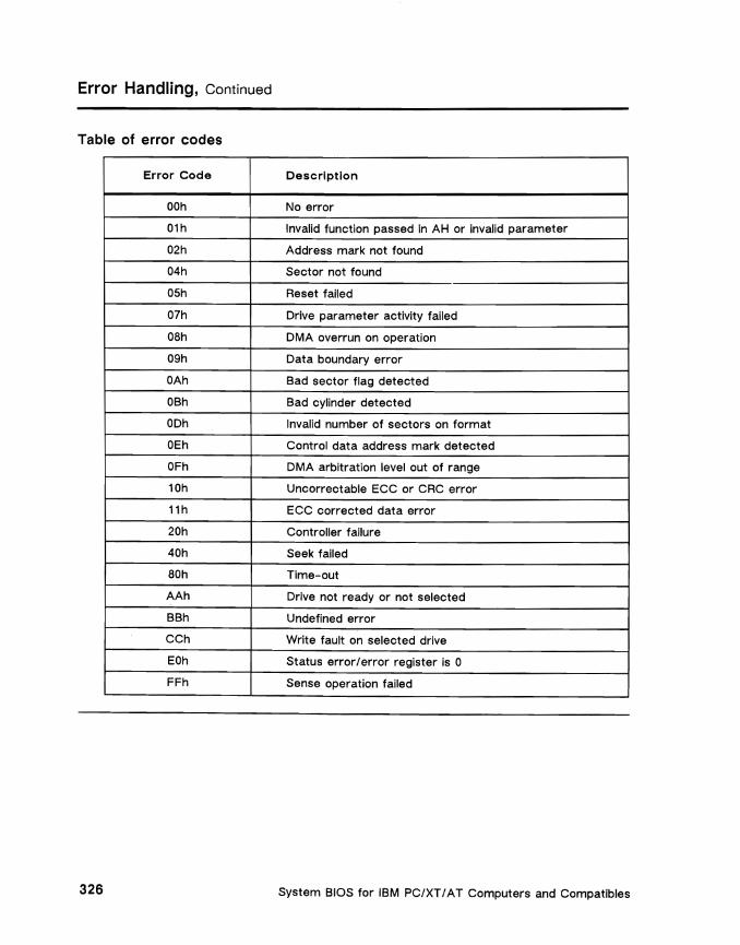
Error Handling, Continued
Table of error codes
Error Code
OOh
01h
02h
04h
OSh
07h
OBh
09h
OAh
OBh
ODh
OEh
OFh
10h
11 h
20h
40h
BOh
AAh
BBh
CCh
EOh
FFh
Description
No error
Invalid function passed in AH or invalid parameter
Address mark not found
Sector not found
Reset failed
Drive parameter activity failed
DMA overrun on operation
Data boundary error
Bad sector flag detected
Bad cylinder detected
Invalid number of sectors on format
Control data address mark detected
DMA arbitration level out of range
Uncorrectable ECC or CRC error
ECC corrected data error
Controller failure
Seek failed
Time-out
Drive not ready or not selected
Undefined error
Write fault on selected drive
Status error/error register is 0
Sense operation failed
System BIOS for IBM PC/XT / AT Computers and Compatibles 326

Function: AH = OOh Reset Diskette(s) and Fixed Disk [XT] [AT]
Description
This function resets both the diskette and the fixed disk controllers. It places both the diskette and the fixed disk systems in a known state by reinitializing the fixed disk and diskette drive parameters and by recalibrating the read/ write heads positions of both devices to cylinder O.
The fixed disk drive number (either 80h or 81 h) is specified in DL. If successful, this function returns with AH set to OOh and the Carry Flag cleared.
Note: The diskette system is reset regardless of the drive number specified in DL. To reset the fixed disk controller only, use Function AH = ODh.
Input/Output
Input: AH OOh
Output: AH = OOh No error xxh Error (See error codes earlier in this chapter)
= Fixed Disk Status (40:74h) CF = o No error
= 1 Error
Differentiating diskette from fixed disk errors
In AT systems, the status of the last Diskette Service operation is stored in Diskette Status (40:41 h), and the status of the last Fixed Disk Service operation is stored in Fixed Disk Status (40:74h).
• If the error code returned in AH by this function pertains to the diskette system, then the value of Diskette Status will be equal to the value of AH.
• If the error code in AH pertains to the fixed disk, then the value in Fixed Disk Status will be equal to the value in AH.
INT 13h Fixed Disk Service 327

Function: AH = 01 h Read Fixed Disk Status [XT] [AT]
Description
This function returns Fixed Disk Status. the error code from the last operation. in the AL register. Before returning to the caller this function sets Fixed Disk Status and AH to OOh and clears the Carry Flag.
Error code 11 h. ECC Data Error. indicates that a recoverable error was detected during a preceding call to Function 02h Read Sectors. See the heading Error Handling earlier in this chapter for a complete list of all codes that may be returned in AL.
Input/Output
Input: AH DL
= =
01 h Drive number 80h Fixed disk 1 81 h Fixed disk 2
Output: AH
AL =
OOh No error xxh Error (See error codes earlier in this chapter) Fixed Disk Status (40:74h) Error code for last operation
System BIOS for IBM PC/XT/ AT Computers and Compatibles 328

Function: AH = 02h Read Sectors [XT] [AT]
Description
This function reads the number of sectors specified in AL from the drive specified in DL to a buffer area defined by ES:BX. This function also reads the two words of Error Correction Code (ECG) associated with that sector and automatically corrects ECC errors. Multisector transfers are terminated after any sector that has a read error. Cylinder number, sector number, and head number are specified in CH, CL, and DH, respectively (see Input! Output below).
If successful, this function returns with the Carry Flag cleared and AH = OOh.
The number of sectors specified in AL must not be zero or greater than 128. Numbers greater than 128 cause a transfer of greater than 64K and thus force a DMA boundary error.
Input/Output
Input: AH 02h AL Number of sectors to read CH = Cylinder num.ber (low 8 bits, zero-based1 \ 0 bAs CL = Cylinder/sector number, where:
Bits 7-6 = cylinder numb~r (high 2 bits) =' \02'+ L"fL
Bits 5-0 = sector number ---......... DH = Hea "'-- (V\N<.. d number (zero-based) _~ b4 SE..c.\~S DL Drive number
80h fixed disk 1 fV' A)< 2 5:~ '"e A'J>S 81 h fixed disk 2
ES:BX = Pointer to buffer
Output: AH = OOh No error = xxh Error (See error codes earlier in this chapter)
Fixed Disk Status (40:74h) AL Number of sectors of data transferred CF = 0 No error
1 Error
continued
\024 x 64 x 2~b
:::- 1£ 1777 I 216 - ~.,+ GaINT 13h Fixed Disk Service 329
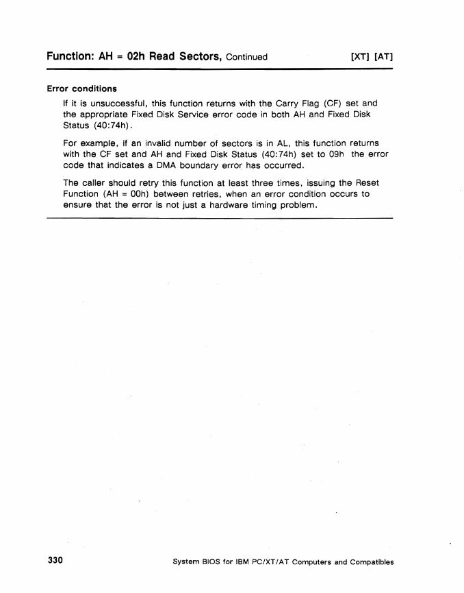
Function: AH = 02h Read Sectors, Continued [XT] [AT]
Error conditions
If it is unsuccessful, this function returns with the Carry Flag (CF) set and the appropriate Fixed Disk Service error code in both AH and Fixed Disk Status (40:74h).
For example, if an invalid number of sectors is in AL, this function returns with the CF set and AH and Fixed Disk Status (40:74h) set to 09h the error code that indicates a DMA boundary error has occurred.
The caller should retry this function at least three times, issuing the Reset Function (AH = OOh) between retries, when an error condition occurs to ensure that the error is not just a hardware timing problem.
System BIOS for IBM PC/XTI AT Computers and Compatibles 330
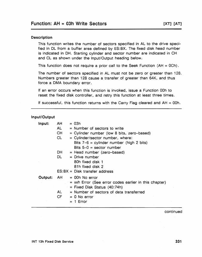
Function: AH= 03h Write Sectors eXT] [AT]
Description
This function writes the number of sectors specified in AL to the drive specified in DL from a buffer area defined by ES:BX. The fixed disk head number is indicated in DH. Starting cylinder and sector number are indicated in CH and CL as shown under the Input/Output heading below.
This function does not require a prior call to the Seek Function (AH = OCh).
The number of sectors specified in AL must not be zero or greater than 128. Numbers greater than 128 cause a transfer of greater than 64K, and thus force a DMA boundary error.
If an error occurs when this function is invoked, issue a Function OOh to reset the fixed disk controller, and retry this function at least three times.
If successful, this function returns with the Carry Flag cleared and AH = OOh.
Input/Output
Input: AH = 03h AL = Number of sectors to write CH = Cylinder number (low 8 bits, zero-based) CL = Cylinder/sector number, where:
Bits 7-6 = cylinder number (high 2 bits) Bits 5-0 = sector number
DH = Head number (zero-based) DL = Drive number
80h fixed disk 1 81 h fixed disk 2
ES:BX = Disk transfer address
Output: AH DOh No error. = xxh Error (See error codes earlier in this chapter) = Fixed Disk Status (40:74h)
AL = Number of sectors of data transferred CF = 0 No error
= 1 Error
continued
INT 13h Fixed Disk Service 331
Function: AH = 03h Write Sectors, Continued [XT] [AT]
Error conditions
If unsuccessful, this function returns with the Carry Flag (CF) set and the appropriate Fixed Disk Service error code in both AH and Fixed Disk Status (40:74h) .
See the Error Handling heading earlier in this chapter for a list of possible errors.
For example, if an invalid number of sectors is in AL, this function returns with CF set and AH and Fixed Disk Status (40:74h) set to 09h, the error code that indicates a DMA boundary error has occurred.
System BIOS for IBM PC/XTIAT Computers and Compatibles 332

Function: AH = 04h Verify Sectors [XT] [AT]
Description
This function verifies the number of sectors specified in AL on the cylinder, head, and drive specified in CH, CL, and DH respectively. (See Input/Output below.)
This function does not compare data on disk with data in memory. It merely verifies that the specified sectors can be read and that the cyclical redundancy check (CRC) is correct. This function does not cause any data to be transferred from memory to fixed disk or vice versa.
If successful, this function returns with the Carry Flag cleared and AH and Fixed Disk Status (40:74h) set to OOh.
Input/Output
Input: AH = 04h AL = Number of sectors to verify CH = Cylinder number (low 8 bits, zero-based) CL = Cylinder/sector number, where:
Bits 7-6 = cylinder number (high 2 bits) Bits 5-0 = sector number
DH = Head number (zero-based) DL Drive number
80h fixed disk 1 81 h fixed disk 2
Output: AH = OOh No error
= xxh Error (See error codes earlier in this chapter)
= Fixed Disk Status (40:74h) AL = Number of sectors verified CF o No error
1 Error
Error conditions
If unsuccessful, this function returns with the Carry Flag (CF) set and the appropriate Fixed Disk Service error code in both AH and Fixed Disk Status (40:74h) .
Refer to the Error Handling heading in this chapter for a table of error codes.
INT 13h Fixed Disk Service 333

Function: AH = 05h Format Cylinder [XT] [AT]
Description
This function formats the cylinder specified in CH and CL using the head specified in DL.
If the system uses an XT -type fixed disk controller, INT 13h, AH = OFh should be called before invoking this function.
Input/Output
Input: AH = 05h AL Interleave factor (XT-type fixed disk controllers only) CH Cylinder number (low 8 bits) CL Cylinder/sector number, where:
Bits 7-6 = cylinder number (high 2 bits, zero-based) Bits 5-0 = sector number
DH Head number (zero-based) DL Drive number
80h fixed disk 1 81 h fixed disk 2
ES: BX = Pointer to table of 2-byte address field entries
Output: AH = OOh No error = xxh Error (See error codes earlier in this chapter) = Fixed Disk Status (40:74h)
CF a No error = 1 Error
continued
System BIOS for IBM PC/XT I AT Computers and Compatibles 334
Function: AH = OSh Format Cylinder, Continued [XT] [AT]
Buffer table contents
The caller must provide a 512-byte table of address markers pointed to by ES:BX. There must be one two-byte table entry for each sector on the cylinder. Table entries must be formatted as shown below:
Byte 1 = good/bad flag OOh is good 80h is bad
Byte 2 = sector number
Example: Address Field Table
For example, the address field to format a track on a fixed disk drive that has an interleave factor of two and that is formatted for 1 7 sectors per track would be:
db 00, 01, 00, OA, 00, 02, 00, OB, 00, 03, 00, OC, 00, 04, 00, 00
db 00, 05, 00, OE, 00, 06, 00, OF, 00, 07, 00, 10, 00, 08, 00, 11
db 00, 09
Error conditions
If unsuccessful, this function returns with the Carry Flag (CF) set and the appropriate Fixed Disk Service error code in both AH and Fixed Disk Status (40:74h). For example, if a time-out error occurs during the execution of this function, error code 80h is returned in both AH and Fixed Disk Status.
If an error occurs when this function is invoked, issue a Function OOh to reset the fixed disk controller and retry this function at least three times.
Refer to the Error Handling heading in this chapter for a table of error codes.
INT 13h Fixed Disk Service 335

Function: AH = 06h Format Bad Track [XT]
Description
This function initializes a track. writing fixed disk address fields and data sectors and setting bad sector flags. It is designed for use with an XT -type fixed disk controller.
For drive 80h. this function references the fixed disk parameter table pointed to by the Interrupt 41 h vector. If successful. this function returns with AH and 40: 74h set to zero.
Input/Output
Input: AH = 06h AL Interleave factor CH = Cylinder number DH = Head number DL = Drive number
80h fixed disk 1 81 h fixed disk 2
Output: AH 07h Drive number in DL is invalid 01 h Invalid function request
= ~Oh If operation is successful xxh Error (See error codes earlier in this chapter) Fixed Disk Status (40:74h)
CF = 0 No error = 1 Error
Error conditions
If an error occurs when this function is invoked. issue a Function OOh to reset the fixed disk controller. and retry this function at least three times.
If the drive number specified in DL is not valid. this function returns with AH and location 40:74h set to 07h to indicate that the drive parameter activity failed. AL. CX. and DX are cleared. the Carry Flag is set. and control is returned to the caller.
System BIOS for IBM PC/XT I AT Computers and Compatibles 336

Function: AH = 07h Format Drive [XT]
Description
This function formats the entire fixed disk drive, writing disk address fields and data sectors, starting at the specified cylinder. This function works only with XT -type fixed disk controllers.
If successful, this function returns with AL and location 40: 74h set to OOh.
Input/Output
Input: AH =~ 01 AL = Interleave factor CH Cylinder DL Drive number
80h fixed disk 1 81 h fixed disk 2
Output: AH = 07h If drive number in DL is invalid OOh No error xxh Error (See error codes earlier in this chapter) Fixed Disk Status (40:74h)
CF 0 No error = 1 Error
Error conditions
If an error occurs when this function is invoked, issue a Function OOh to reset the fixed disk controller, and retry this function at least three times.
If the drive number specified in DL is not valid, this function returns with AH and location 40:74h set to 07h to indicate that the drive parameter activity failed. AL, CX, and OX are cleared, the Carry Flag is set, and control is returned to the caller.
INT 13h Fixed Disk Service 337

Function: AH = OSh Read Drive Parameters [XT] [AT]
Description
This function returns parameters associated with the fixed disk drive (either 80h or 81h) specified in DL.
For drive 80h. this function references the fixed disk parameter table pointed to by the INT 41h vector. For drive 81h. the function references the INT 46h vector. See the ROM BIOS Data heading in this chapter for the structure and contents of the fixed disk parameter table.
If successful. this function returns with AL and Fixed Disk Status set to OOh. The maximum usable cylinder number is returned in CH/CL. maximum usable sector number in CL. maximum usable head number in DH. the number of fixed disk drives contained in the system is returned in DL. and the address of the fixed disk parameter table is returned in ES:DI.
Input/Output
Input: AH = 08h DL Drive number
80h fixed disk 1 81 h fixed disk 2
Output: AH 07h If drive number in DL is invalid
= OOh If operation is successful xxh Error (See error codes earlier in this chapter)
= Fixed Disk Status (40:74h) AL = OOh CF o No error
1 Error CH Maximum usable cylinder number (low 8 bits.
zero-based) (OOh if AH = 07h)
CL Cylinder/sector number. where: Bits 7-0 = OOh if AH = 07h Bits 7-6 = Maximum usable cylinder number (high 2 bits) Bits 5-0 = Maximum usable sector number
DH Maximum usable head number DL = Number of drives (zero-based. OOh if AH = 07h) ES:DI Address of fixed disk parameter table
continued
System BIOS for IBM PC/XT/ AT Computers and Compatibles 338

Function: AH = OSh Read Drive Parameters, Continued [XT] [AT]
Error conditions
If the drive number specified in DL is not valid. this function returns with AH and Fixed Disk Status (40:74h) set to 07h to indicate that the drive parameter activity failed. AL. CX. and DX are cleared. the Carry Flag is set. and control is returned to the caller.
INT 13h Fixed Disk Service 339
Function: AH ::: 09h Initialize Drive Parameters [XT] [AT]
Description
This function initializes the controller associated with the fixed disk drive (either 80h or 81 h) specified in DL.
For drive 80h, this function references the fixed disk parameter table pointed to by the Interrupt 41 h vector. For drive 81 h, the function uses the interrupt 46h vector. See the ROM BIOS Data heading in this chapter for the structure and contents of the fixed disk parameter table.
If successful, thiS function returns with AH and Fixed Disk Status (40:74h) set and the Carry Flag cleared.
Input/Output
Input: AH = 09h DL = Drive number
80h fixed disk 1 81 h fixed disk 2
Output: AH = OOh No error = 07h Operation has failed = xxh Error (See error codes earlier in this chapter)
Fixed Disk Status (40:74h) CF = 0 No error
= 1 Error
Error conditions
If unsuccessful, the Initialize Drive Parameters function returns with AH and Fixed Disk Status (40:74h) equal to 07h. This indicates that drive parameter activity has failed.
Note: The Initialize Drive Parameters function generates only two valid return codes:
AH = Fixed Disk Status = OOh = Function successful AH Fixed Disk Status = 07h = Function unsuccessful,
drive parameter activity has failed.
System BIOS for IBM PC/XT / A T Computers and Compatibles 340
Function: AH = OAh Read Long Sectors [XT] [AT]
Description
This function reads one or more sectors from the fixed disk specified in Dl. This function also reads the four to seven bytes of Error Correction Code (ECC) associated with that sector, but does not automatically correct ECC errors (Function 02h automatically corrects ECC errors). Multisector transfers are terminated after any sector that has a read error. Cylinder number, sector number, and head number are specified in CH, Cl, and DH, respectively.
This function does not require a prior call to the Seek Function (AH = OCh).
This function is normally reserved for diagnostics and should not be used for normal reads from the fixed disk.
If successful, this function returns with the Carry Flag cleared and AH and Fixed Disk Status (40:74h) equal to zero.
Input/Output
Input: AH OAh Al = Number of sectors (usually one) CH Cylinder number (low 8 bits, zero-based) Cl Cylinder/sector number, where:
Bits 7-6 = cylinder number (high 2 bits) Bits 5-0 = sector number
DH Head number (zero-based) Dl Drive number
80h fixed disk 1 81 h fixed disk 2
ES:BX = Disk transfer address
Output: AH OOh No error xxh Error (See error codes earlier in this chapter)
= Fixed Disk Status (40:74h) CF = 0 No error
= 1 Error
continued
INT 13h Fixed Disk Service 341

Function: AH = OAh Read Long Sectors, Continued [XT] [AT]
Error conditions
If unsuccessful, this function returns with the Carry Flag (CF) set and the appropriate Fixed Disk Service error code in both AH and in Fixed Disk Status (40:74h).
For example, if the number of sectors in AL is not 01 h, this function returns with AH and Fixed Disk Status (40:74h) set to 01 h (the invalid parameter error code) and the Carry Flag set.
Refer to the Error Handling heading in this chapter for a table of error codes.
System BIOS for IBM PC/XTIAT Computers and Compatibles 342

Function: AH = OBh Write Long Sectors [XT] [AT]
Description
This function writes one or more sectors to the location on the fixed disk specified in Dl from the buffer pointed to by ES:BX. This function also writes four to seven bytes of Error Correction Code (ECC) associated with the specified sectors.
Cylinder number, sector number, and head number are specified in CH, Cl, and DH, respectively (see Input/Output below).
This function does not require a prior call to Function OCh, Seek to Cylinder.
Along with Function AH = OAh, this function is normally reserved for diagnostics and should not be used for normal write to fixed disk operations.
If successful, this function returns with the Carry Flag cleared and AH and Fixed Disk Status (40:74h) equal to zero.
Input/Output
Input: AH = OBh Al = Number of sectors to write (usually one) CH = Cylinder number (low 8 bits, zero-based) Cl = Cylinder/sector number, where:
Bits 7-6 =cylinder number (high 2 bits) Bits 5-0 = sector number
DH = Head number (zero-based) Dl = Drive number
80h fixed disk 1 81 h fixed disk 2
ES:BX = Disk transfer address
Output: AH = OOh No error = xxh Error (See error codes earlier in this chapter) = Fixed Disk Status (40:74h)
CF = 0 No error = 1 Error
continued
INT 13h Fixed Disk Service 343

Function: AH = aSh Write Long Sectors, Continued [XT] [AT]
Error conditions
If unsuccessful, this function returns to the caller with the Carry Flag (CF) set and the appropriate Fixed Disk Service error code in both AH and in Fixed Disk Status (40:74h).
Refer to the Error Handling heading in this chapter for a table of error codes.
System BIOS for IBM PC/XT I AT Computers and Compatibles 344

Function: AH = OCh Seek to Cylinder [XT] [AT]
Description
This function positions the disk read/write head over the cylinder specified in CH and CL (see Input/Output below). The fixed disk drive number must be specified in DL.
If successful, this function returns with the Carry Flag cleared and AH and Fixed Disk Status (40:74h) equal to zero.
The Read Disk Sectors (AH = 02h), Write Disk Sectors (AH = 03h), Read Long Sectors (AH = OAh) , and Write Long Sectors (AH = OBh) functions have a seek operation implicitly built into them and do not require a prior call to this function.
Input/Output
Input: AH = OCh CH Cylinder number (low 8 bits, zero-based) CL Cylinder/sector number, where:
Bits 7-6 = cylinder number (high 2 bits) Bits 5-0 = sector number
DH = Head number (zero-based) DL = Drive number
80h fixed disk 1 81 h fixed disk 2
Output: AH = OOh No error = xxh Error (See error codes earlier in this chapter) = Fixed Disk Status (40:74h)
CF 0 No error = 1 Error
Error conditions
If unsuccessful, this function returns to the caller with the Carry Flag (CF) set and the appropriate Fixed Disk Service error code in both AH and in Fixed Disk Status (40: 7 4h) .
Refer to the Error Handling heading in this chapter for a table of error codes.
INT 13h Fixed Disk Service 345

Function: AH = ODh Alternate Fixed Disk Reset [XT] [AT]
Description
This function is identical to INT 13h AH = OOh Reset Diskette (s) and Fixed Disk except that the diskette system is not reset.
The caller must specify the fixed disk drive to reset in DL. This function reinitializes the fixed disk controller and places the specified fixed disk drive in a known state by resetting the fixed disk parameters and by recalibrating the read/write head positions. This process resets the read/writer head to track O.
If successful, this function returns with the Carry Flag cleared and AH and Fixed Disk Status (40:74h) equal to zero.
Input/Output
Input: AH ODh DL Drive number
80h fixed disk 1 81 h fixed disk 2
Output: AH = OOh No error = xxh Error (See error codes earlier in this chapter)
Fixed Disk Status (40:74h) CF = 0 No error
1 Error
Error conditions
If not successful, this function returns to the caller with the Carry Flag (CF) set and the appropriate Fixed Disk Service error code in both AH and in Fixed Disk Status (40:74h).
Refer to the Error Handling heading in this chapter for a table of error codes.
System BIOS for IBM PC/XT/AT Computers and Compatibles 346
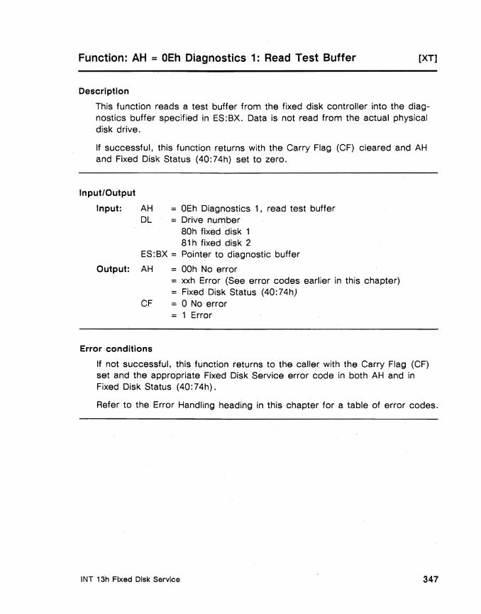
Function: AH = OEh Diagnostics 1: Read Test Buffer [XT]
Description
This function reads a test buffer from the fixed disk controller into the diagnostics buffer specified in ES:BX. Data is not read from the actual physical disk drive.
If successful, this function returns with the Carry Flag (CF) cleared and AH and Fixed Disk Status (40:74h) set to zero.
Input/Output
Input: AH = OEh Diagnostics 1, read test buffer DL = Drive number
80h fixed disk 1 81 h fixed disk 2
ES:BX = Pointer to diagnostic buffer
Output:· AH OOh No error = xxh Error (See error codes earlier in this chapter)
Fixed Disk Status (40:74h) CF 0 No error
= 1 Error
Error conditions
If not successful, this function returns to the caller with the Carry Flag (CF) set and the appropriate Fixed Disk Service error code in both AH and in Fixed Disk Status (40: 74h) .
Refer to the Error Handling heading in this chapter for a table of error codes.
INT 13h Fixed Disk Service 347
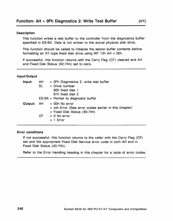
Function: AH = OFh Diagnostics 2: Write Test Buffer [XT]
Description
This function writes a test buffer to the controller from the diagnostics buffer specified in ES:BX. Data is not written to the actual physical disk drive.
This function should be called to initialize the sector buffer contents before formatting an XT -type fixed disk drive using INT 13h AH = 05h.
If successful. this function returns with the Carry Flag (CF) cleared and AH and Fixed Disk Status (40:74h) set to zero.
Input/Output
Input: AH = OFh Diagnostics 2. write test buffer DL = Drive number
80h fixed disk 1 81 h fixed disk 2
ES:BX = Pointer to diagnostic buffer
Output: AH = OOh No error xxh Error (See error codes earlier in this chapter) Fixed Disk Status (40:74h)
CF = 0 No error = 1 Error
Error conditions
If not successful. this function returns to the caller with the Carry Flag (CF) set and the appropriate Fixed Disk Service error code in both AH and in Fixed Disk Status (40:74h).
Refer to the Error Handling heading in this chapter for a table of error codes.
System BIOS for IBM PC/XT/ AT Computers and Compatibles 348

Function: AH = 10h Test for Drive Ready [XT] [AT]
Description
This function determines if the fixed disk drive specified in DL is ready and can process a command.
If successful, this function returns to the caller with the Carry Flag (CF) cleared and AH and Fixed Disk Status (40:74h) set to zero.
Input/Output
Input: AH 10h DL Drive number
80h fixed disk 1 81 h fixed disk 2
Output: AH = OOh No error xxh Error (See error codes earlier in this chapter) Fixed Disk Status (40:74h)
CF = 0 No error = 1 Error
Error conditions
If not successful, this function returns to the caller with the Carry Flag (CF) set and the appropriate Fixed Disk Service error code in both AH and in Fixed Disk Status (40:74h).
Refer to the Error Handling heading in this chapter for a table of error codes.
INT 13h Fixed Disk Service 349

Function: AH = 11 h Recalibrate Drive [XT] [AT]
Description
This function repositions head 0 over cylinder 0 of the fixed disk drive specified in DL.
If successful, this function returns with the Carry Flag (CF) cleared and AH and Fixed Disk Status (40:74h) set to zero.
Input/Output
Input: AH = 11 h DL Drive number
80h fixed disk 1 81 h fixed disk 2
Output: AH = OOh No error = xxh Error (See error codes earlier in this chapter) = Fixed Disk Status (40:74h)
CF = 0 No error = 1 Error
Error conditions
If not successful, this function returns to the caller with the Carry Flag (CF) set and the appropriate Fixed Disk Service error code in both AH and in Fixed Disk Status (40:74h).
Refer to the Error Handling heading in this chapter for a table of error codes.
System BIOS for IBM PC/XTI AT Computers and Compatibles 350

Function: AH = 12h Controller RAM Diagnostic eXT]
Description
This function causes the fixed disk controller to carry out a built-in diagnostic test on its internal sector buffer, indicating whether the test was passed by a status indicator in AH.
Input/Output
Input: AH AL
= =
12h Number of sectors
CH CL
= Cylinder Sector
DH = Head DL Drive number
80h fixed disk 1 81 h fixed disk 2
Output: AL AH
= =
OOh OOh No error
CF = =
xxh Error (See error codes earlier in this chapter) Fixed Disk Status (40:74h) o No error
= 1 Invalid parameter
Error conditions
If not successful, this function returns with the appropriate Fixed Disk Service error code in both AH and location 40:74h and the Carry Flag (CF) set.
Refer to the Error Handling heading in this chapter for a table of error codes.
INT 13h Fixed Disk Service 351
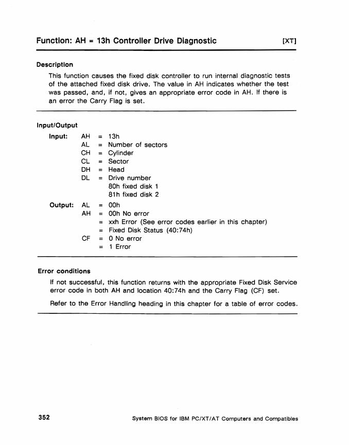
Function: AH = 13h Controller Drive Diagnostic [XT]
Description
This function causes the fixed disk controller to run internal diagnostic tests of the attached fixed disk drive. The value in AH indicates whether the test was passed, and, if not, gives an appropriate error code in AH. If there is an error the Carry Flag is set.
Input/Output
Input: AH = 13h AL = Number of sectors CH = Cylinder CL = Sector DH = Head DL = Drive number
80h fixed disk 1 81 h fixed disk 2
Output: AL = OOh AH = OOh No error
= xxh Error (See error codes earlier in this chapter) Fixed Disk Status (40:74h)
CF = o No error = 1 Error
Error conditions
If not successful, this function returns with the appropriate Fixed Disk Service error code in both AH and location 40:74h and the Carry Flag (CF) set.
Refer to the Error Handling heading in this chapter for a table of error codes.
System BIOS for IBM PC/XT I AT Computers and Compatibles 352
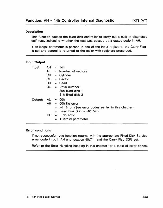
Function: AH = 14h Controller Internal Diagnostic [XT] [AT]
Description
This function causes the fixed disk controller to carry out a built-in diagnostic self-test, indicating whether the test was passed by a status code in AH.
If an illegal parameter is passed in one of the input registers, the Carry Flag is set and control is returned to the caller with registers preserved.
Input/Output
Input: AH AL =
14h Number of sectors
CH CL
= =
Cylinder Sector
DH Head DL = Drive number
80h fixed disk 1 81 h fixed disk 2
Output: AL AH
= OOh OOh No error
CF
= = =
xxh Error (See error codes earlier in this chapter) Fixed Disk Status (40:74h) o No error
= 1 Invalid parameter
Error conditions
If not successful, this function returns with the appropriate Fixed Disk Service error code in both AH and location 40:74h and the Carry Flag (CF) set.
Refer to the Error Handling heading in this chapter for a table of error codes.
INT 13h Fixed Disk Service 353
Function: AH = 15h Read Fixed Disk Type [AT]
Description
This function returns a status code in AH which indicates the type of diskette or fixed disk drive for the drive specified in DL. This function also returns the number of 512-byte blocks on the fixed disk if the drive specified in DL is valid. (Valid values are 80h and 81 h.)
If successful, the high word of the number of 512-byte sectors on the fixed disk is returned in CX, and the low word of the number of 512-byte sectors is returned in OX. The Fixed Disk Status (40:74h) and AH are set to OOh, the Carry Flag is cleared, and control is returned to the caller.
Input/Output
Input: AH = 15h DL Drive number
80h fixed disk 1 81 h fixed disk 2
Output: AH = OOh No drive installed = 03h Fixed disk was accessed = xxh Error (See error codes earlier in this chapter) = Fixed Disk Status (40:74h)
CF = 0 No error = 1 Error
CX = Number of 512-byte sectors on the fixed disk (valid only of AH = 03h)
continued
System BIOS for IBM PC/XTIAT Computers and Compatibles 354

Function: AH = 15h Read Fixed Disk Type, Continued [AT]
AHreports drive number validity
For drive 80h, this function references the fixed disk parameter table pointed to by the Interrupt 41 h vector. For drive 81 h, the function references the Interrupt 46h vector.
Unlike most other Fixed Disk Service functions, in this function the value stored in AH is not equal to the value stored in Fixed Disk Status (40: 74h). Instead, AH reports whether or not the drive number input in DL is valid (AH will equal OOh if there is no drive for this drive number), or the fixed disk/ diskette status of the drive specified in DL.
Error conditions
If the drive number specified in DL is not valid, this function clears AH, AL, CX, OX, and the Fixed Disk Status (40:74h), clears the Carry Flag, and returns control to the caller.
INT 13h Fixed Disk Service 355

Chapter 12
INT 14h Serial Communications Service
Overview
Description
The BIOS Serial Communications Service performs RS-232C character I/O on IBM-compatible serial port adapters.
How the Serial Communications Service is invoked
Software INT 14h invokes the Serial Communications Service.
The INT 14h vector resides at address OO:50h in the interrupt vector table. The BIOS initializes the INT 14h vector to address FOOO:E739h.
continued
INT 14h Serial Commu.nications Service 357

Overview, Continued
Summary of Serial Communications functions
The Serial Communications Service contains four functions. Individual functions are selected via the AH register. The table below summarizes the Serial Communications Service functions.
Function Description Platforms
OOh Initialize Serial Communications Port tXT) [AT)
01h Send Character tXT) [AT)
02h Receive Character tXT) [AT)
03h Read Serial Port Status tXT) [AT)
04h-FFh Reserved Reserved
In this chapter
This chapter focuses on the BIOS Serial Communications Service. The following topics are discussed:
• Theory of Operation
• System RAM Data
• ROM BIOS Data
• Serial Communications I/O Ports
• Error Conditions
• Serial Communications Functions
How to determine level of support
Legend Description
[PC) Function Is supported by original IBM PC BIOS only.
tXT) Function is supported by all IBM PC/XT and compatible ROM BlOSs.
Note: This level of support is contained in the ROM BIOS implemented in the majority of IBM PC and PC/XT compatible systems.
[AT) Function is supported by all IBM PCIA T and compatible ROM BlOSs.
System BIOS for IBM PC/XT I A T Computers and Compatibles 358
Theory of Operation
Introduction
The asynchronous serial port on an IBM PC, PC/XT, and PC/AT converts data from parallel form to serial form for communication between the computer and an external device, usually a serial printer or an external modem. The physical connection consists of an RS-232C-standard cable linking the two devices. The ROM BIOS Serial Communications Service. which is invoked via INT 14h, performs various operations that make serial transmission and reception possible.
Parallel and serial transmission
In a parallel connection, all the individual bits of a data byte are simultaneously transmitted over the parallel port. This kind of connection exists between a computer and a parallel printer. When data is transmitted serially. however. all the bits of a data byte are sequentially transmitted over the serial port. For example, during serial transmission, a parallel data byte of 8 bits would be converted to a serial data byte of 8 consecutive data bits. delivered one at a time. The receiving device then assembles these individual bits into a parallel data byte.
continued
INT 14h Serial Communications Service 359

Theory of Operation, Continued
Data sent as packets of frames
Since asynchronous serial transmission sends individual data bits along the lID path, there has to be some way for the receiver to distinguish these bits and assemble them into separate characters. This is achieved through the serial controller, which packages each data byte into a separate frame. Each frame consists of a start bit, the actual data byte, an optional parity bit, and a stop bit (s) .
The start bit is automatically inserted by the controller before it sends a character. This is the first bit that the receiving device gets, and it tells the device that a character is about to follow. The data byte, which can be a 5-, 6-, 7-, or a-bit character, follows the start bit. If the controller is programmed to add an error-detecting parity bit, this comes next. Finally, the stop bits complete the frame. These tell the receiving device that this is the end of a character and another one is about to begin. The controller can be programmed to insert 1, 1.5, or 2 stop bits.
Sending characters as packets of frames allows the receiving device to recognize when a particular character begins and ends, so that these characters can be distinguished and joined into words.
NS 16450 IC Controller
The Serial Communications Service assumes a National Semiconductor NS 16450 IC serial communications controller (or compatible) is in place. The controller contains a programmable baud rate generator that supports baud rates from 50 baud to 9600 baud. The controller also supports 5-, 6-, 7-, and a-bit characters with 1-, 1.5-, or 2-stop bits operating in even, odd, and no parity modes.
continued
System BIOS for IBM PC/XT/AT Computers and Compatibles 360
Theory of Operation, Continued
RS-232C interface standard
All IBM and compatible serial controllers use a predetermined standard (called an interface) for sending and receiving serial data. This interface standard is called the RS-232C. The RS-232C interface standard defines various connection parameters, including the connector type, 1/0 signal levels, line names, and pin numbers.
The cable that links the computer's serial port to the external device must conform to EIA RS-232C (or equivalent) standards.
Programming the controller
The serial communications controller is responsible for performing a host of operations on the incoming or outgoing serial data stream. For one, the controller adds or removes bits as described above. In addition, the controller controls the speed at which data gets sent across the the data path. Also, the controller communicates with the external device through signals that inform the two devices about their readiness to send and receive data (see 1/0 signals on the next page).
All of these operations can be modified by programming the controller. The controller can be programmed by manipulating the serial communications 1/0 ports.
Reference: A complete list of the serial 1/0 ports can be found under the heading Serial Communications 1/0 Ports in this chapter.
continued
INT 14h Serial Communications Service 361
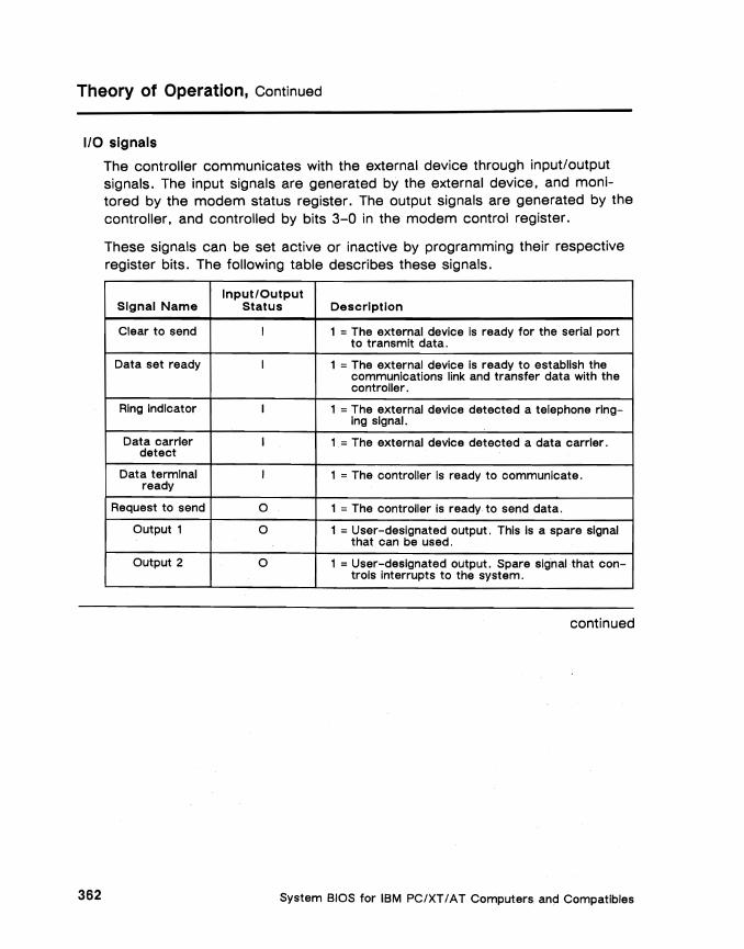
Theory of Operation, Continued
1/0 signals
The controller communicates with the external device through input/output signals. The input signals are generated by the external device, and monitored by the modem status register. The output signals are generated by the controller, and controlled by bits 3-0 in the modem control register.
These signals can be set active or inactive by programming their respective register bits. The following table describes these signals.
Input/Output Signal Name Status Description
Clear to send I 1 = The external device Is ready for the serial port to transmit data.
Data set ready I 1 = The external device Is ready to establish the communications link and transfer data with the controller.
Ring Indicator I 1 =The external device detected a telephone ring-Ing signal.
Data carrier I 1 . =The external device detected a data carrier. detect
Data terminal ready
I 1 =The controller Is ready to communicate.
Request to send 0 1 = The controller is ready to send data,
Output 1 0 1 =User-designated output. This is a spare signal that can be used.
Output 2 0 1 =User~deslgnated output, Spare sig'nal that controls Interrupts to the system,
continued
System BIOS for IBM PC/XT / AT Computers and Compatibles 362
Theory of Operation, Continued
INT 14h and the serial port
The ROM BIOS Serial Communications Service is invoked via INT 14h, and its functions perform various serial I/O operations on IBM-compatible serial port adapters and controllers. This service contains functions that initialize the serial port, transmit a character across the I/O path, receive a character, and read the status of the serial port.
INT 14h and data transmission
The process whereby an INT 14h request causes data to be transmitted across the RS-232C I/O path is:
1. A program places the data byte to be sent in AL, puts Function 01 h Send Character in AH, and performs an INT 14h.
2. The BIOS transfers the data in AL to the serial port specified in ox. The serial controller and the external device communicate through a series of signals. These signals, such as Data terminal ready (OTR) and Request to send (RTS) , relay control information across the I/O path. When the external device signals that it is ready to begin the data transfer, the controller inserts the appropriate bits before and after each data byte and sends each frame across the I/O path.
3. The external device receives each character, removes the start, parity, and stop bits, and assembles the characters.
continued
INT 14h Serial Communications Service 363

Theory of Operation, Continued
Serial data flow
The graphic below traces the path of serial data from the controller to the receiving device.
Calling Program
Port Specified In DX
Parity Bit Start Bit
External Device
I- - - One Frame - - --I
System BIOS for IBM PC/XT /AT Computers and Compatibles 364
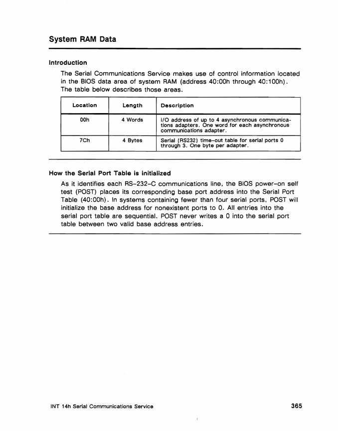
System RAM Data
Introduction
The Serial Communications Service makes use of control information located in the BIOS data area of system RAM (address 40:00h through 40:100h). The table below describes those areas.
Location Length Description
OOh 4 Words I/O address of up to 4 asynchronous communications adapters. One word for each asynchronous communications adapter.
7Ch 4 Bytes Serial (RS232) time-out table for serial ports 0 through 3. One byte per adapter.
How the Serial Port Table is initialized
As it identifies each RS-232-C communications line, the BIOS power-on self test (POST) places its corresponding base port address into the Serial Port Table (40:00h). In systems containing fewer than four serial ports, POST will initialize the base address for nonexistent ports to O. All entries into the serial port table are sequential. POST never writes a 0 into the serial port table between two valid base address entries.
INT 14h Serial Communications Service 365

ROM BIOS Data
Baud rate initialization table
The baud rate initialization table is located at FOOO:E729h in the ROM BIOS. The table is structured as follows:
Baud Rate Divisor
110 0417h
150 0300h
300 0180h
600 OOCOh
1200 0060h
2400 0030h
4800 0018h
9600 OOOCh
How baud rate divisor is calculated
The controller's clock input runs at 1.8432 MHz. The values in the table are calculated as follows:
1,843,200 115200 = = Divisor
16 Baud Rate
For example, a baud rate of 2400 has a divisor of 115200/2400, which equals 48 decimal, 30 hex.
System BIOS for IBM PC/XTIA T Computers and Compatibles 366

Serial Communications 1/0 Ports
INT 14h references the following 1/0 ports. These registers are used to monitor the controller's operations, and to transmit and receive data.
Read/Write 1/0 Address Status Description
03F8h W Serial 1, transmitter holding register, which contains the character to be sent. Bit 0, the least significant bit, is sent first. Bits 7-0 = Contains data bits 7-0, respec
tlvely, when Divisor Latch Access Bit (DLAB) = 0
03F8h R Serial 1, receiver buffer register, which contains the received character. Bit 0, the least significant bit, Is sent first. Bits 7-0 = Contains data bits 7-0, respec
tively, when DLAB = 0
03F8h R/W Serial 1, divisor latch, low byte. Both divisor latch registers store the baud rate divisor. Bits 7-0 = Bits 7-0 of divisor, when DLAB = 1
03F9h R/W Serial 1, divisor latch, high byte, where: Bits 7-0 = Bits 15-8 of divisor, when DLAB = 1
03F9h R/W Serial 1, interrupt enable register. Allows the four controller interrupts to enable the chip-Interrupt output signal. Bits 7-4 = 0 Reserved Bit 3 = 1 Modem-status interrupt enable Bit 2 = 1 Receiver-line-status interrupt
enable Bit 1 = 1 Transmitter-holding-register
empty interrupt enable Bit 0 = 1 Received-data-available interrupt
enable when DLAB = 0
continued
INT 14h Serial Communications Service 367

Serial Communications 1/0 Ports, Continued
Read/Write I/O Address Status Description
03FAh R Serial 1 Interrupt ID register. Information about a pending Interrupt Is stored here. When ID register Is addressed. the highest priority interrupt is held and no other Interrupts are acknowledged until the CPU services that Interrupt. Bits 7-3 =0 Reserved Bits 2-1 =These bits identify the pending in
terrupt with the highest priority: llb Receiver Line Status Interrupt,;
lOb priority =highest. Received Data Available;
Bit 0
priority =second 01b Transmitter Holding Register;
priority = third. OOb Modem Status Interrupt;
priority = fourth. =0 Interrupt pending. and contents of
register can be used as a pointer to the appropriate Interrupt service routine.
=1 No interrupt pending.
03FBh R/W Serial 1. line control register. where: Bit 7 =0 Receiver Buffer. Transmitter
Holding. or Interrupt Enable Registers Access
=1 Divisor Latch Access Bit 6 =1 Set Break Enabled. Serial output is
forced to spacing state and remains there.
Bit 5 Bit 4 Bit 3
=Stick Parity =Even Parity Select =Parity Enable =1 Even number of ones are sent and
checked In the data word bits and parity bit. if Bit 3 is 1.
=0 Odd number of ones are sent and checked. if Bit 3 is 1.
Bit 2 =Specify number of stop bits per character:
=01 Stop Bit =1 0 Stop Bits
Bits 1-0 =Specify the number of bits per character: OOb 5 Bit Word Length 01 b 6 Bit Word Length lOb 7 Bit Word Length 11 b 8 Bit Word Length
continued
System BIOS for IBM PC/XT / AT Computers and Compatibles 368
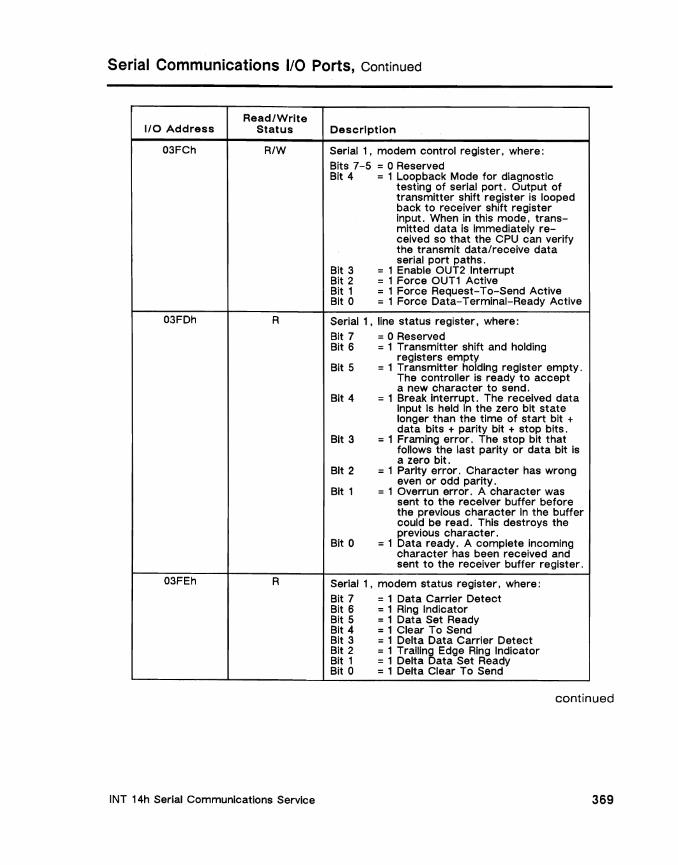
Serial Communications 1/0 Ports, Continued
Read/Write I/O Address Status Description
03FCh R/W Serial 1, modem control register, where: Bits 7-5 =0 Reserved Bit 4 = 1 Loopback Mode for diagnostic
testing of serial port, Output of transmitter shift register is looped back to receiver shift register Input. When in this mode, transmitted data is immediately received so that the CPU can verify the transmit data/receive data serial port paths.
Bit 3 Bit 2
= 1 Enable OUT21nterrupt = 1 Force OUT1 Active
Bit 1 Bit 0
= 1 Force Request-To-Send Active = 1 Force Data-Terminal-Ready Active
03FDh R Serial 1, line status register, where:
Bit 7 =0 Reserved Bit 6
Bit 5
=1 Transmitter shift and holding registers empty
=1 Transmitter holding register empty. The controller is ready to accept a new character to send.
Bit 4 =1 Breaklnterrupt. The received data input Is held In the zero bit state longer than the time of start bit + data bits + parity bit + stop bits.
Bit 3 =1 Framing error. The stop bit that follows the last parity or data bit is a zero bit.
Bit 2
Bit 1
=1 Parity error. Character has wrong even or odd parity.
=1 Overrun error. A character was sent to the receiver buffer before the previous character In the buffer could be read. This destroys the previous character.
Bit 0 =1 Data ready. A complete incoming character has been received and sent to the receiver buffer register.
03FEh R Serial 1, modem status register, where: Bit 7 =1 Data Carrier Detect Bit 6 =1 Ring Indicator Bit 5 Bit 4
=1 Data Set Ready =1 Clear To Send
Bit 3 =1 Delta Data Carrier Detect Bit 2 Bit 1 Bit 0
=1 Trailing Edge Ring Indicator =1 Delta Data Set Ready =1 Delta Clear To Send
continued
INT 14h Serial Communications Service 369

Serial Communications 1/0 Ports, Continued
ReadlWrite 1/0 Address Status Description
03FFh R/W Serial 1. Reserved
02F8h W Serial 2. transmitter holding register. which contains the character to be sent. Bit O. the least significant bit. is sent first. Bits 7-0 =Contains data bits 7-0. respec
tively. when Divisor Latch Access Bit (DLAB) =0
.02F8h R Serial 2. receiver buffer register. which con
tains the received character. Bit O. the least significant bit. is first to be sent. Bits 7-0 =Contains data bits 7-0. respectively.
when DLAB =0
02F8h R/W Seriai 2. divisor latch. low byte. where; Bits 7-0 =Bits 7-0 of divisor. when DLAB =1
02F9h R/W Serial 2. divisor latch. high byte. where: Bits 7-0 =Bits 15-8 of divisor. when DLAB =1
02F9h R/W Serial 2. interrupt enable register. Allows the four controller interrupts to enable the chip-Interrupt output signal. Bits 7-4 =0 Reserved Bit 3 =1 Modem-status interrupt enable Bit 2 =1 Receiver-line-status interrupt
enable Bit 1 =1 Transmitter-holding-register
empty interrupt enable Bit 0 =1 Received-data-avallable interrupt
enable when DLAB =0
02FAh R Serial 2 interrupt I D register. Information about a pending interrupt is stored here. When ID register is addressed. the highest priority interrupt is held and no other interrupts are acknowledged until the CPU services that Interrupt. Bits 7-3 =0 Reserved Bits 2-1 =These bits identify the pending Inter
rupt with the highest priority: 11b Receiver Line Status Interrupt;
priority =highest. 10b Received Data Available;
priority =second 01b Transmitter Holding Register;
priority =third. OOb Modem Status Interrupt;
priority =fourth. Bit 0 =0 Interrupt pending. and contents of
register can be used as a pointer to the appropriate Interrupt service routine.
=1 No Interrupt pending.
continued
370 System BIOS for IBM PC/XTI A T Computers and Compatibles
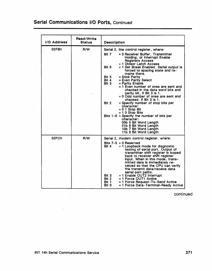
Serial Communications 110 Ports, Continued
Read/Write I/O Address Status
02FBh R/W
02FCh R/W
Description
Serial 2, line control register, where: Bit 7 = 0 Receiver Buffer, Transmitter
Holding, or Interrupt Enable Registers Access
=1 Divisor Latch Access Bit 6 =1 Set Break Enabled. Serial output is
forced to spacing state and remains there.
Bit 5 =Stick Parity Bit 4 =Even Parity Select Bit 3 =Parity Enable
=1 Even number of ones are sent and checked In the data word bits and parity bit, If Bit 3 Is 1.
=0 Odd number of ones are sent and checked, If Bit 3 Is 1.
Bit 2 =Specify number of stop bits per character:
=01 Stop Bit =1 0 Stop Bits
Bits 1-0 =Specify the number of bits per character: OOb 5 Bit Word Length 01 b 6 Bit Word Length 10b 7 Bit Word Length 11 b 8 Bit Word Length
Serial 2, modem control register, where: Bits 7-5 =0 Reserved Bit 4 =1 Loopback mode for diagnostic
testing of serial port. Output of transmitter shift register Is looped back to receiver shift register Input. When In this mode, transmitted data is Immediately received so that the CPU can verify the transmit data/receive data serial port paths.
Bit 3 =1 Enable OUT2 Interrupt Bit 2 . = 1 Force OUT1 Active Bit 1 =1 Force Request-To-Send Active Bit 0 =1 Force Data-Terminal-Ready Active
continued
INT 14h Serial Communications Service 371

Serial Communications 1/0 Ports, Continued
ReadlWrite 1/0 Address Status
02FDh R
02FEh R
02FFh R/W
3220-322Bh R/W
322B-322Fh R/W
Description
Serial 2, line status register, where: Bit 7 =0 Reserved Bit 6 =1 Transmitter shift and holding . registers empty . Bit 5 =1 Transml.tter holding register empty.
The controller Is ready to accept a new character to send.
Bit 4 =1 Break interrupt. The received data input is held in the zero bit state longer than the time of start bit + data bits + parity bit + stop bits.
Bit 3 =1 Framing error. The stop bit that follows the last parity or data bit is a zero bit.
Bit 2 =1 Parity error. Character has wrong ~ven or odd parity.
Bit 1 =1 Overrun error. A character was sent to the receiver buffer before the previous character in the buffer could be read. This destroys the previous character.
Bit 0 =1 Data ready. A complete incoming character has been received and sent to the receiver buffer register.
Serial 2, modem status register, where: Bit 7 =1 Data Carrier Detect Bit 6 =1 Ring Indicator Bit 5 =1 Data Set Ready Bit 4 =1 Clear To Send Bit 3 =1 Delta Data Carrier Detect Bit 2 =1 Trailing Edge Ring Indicator Bit 1 =1 Delta Data Set Ready Bit 0 =1 Delta Clear To Send
Serial 2, Reserved
Often used for serial port 3 (see 1/0 address descriptions for 03FBh-03FFh for details).
Often used for serial port 3 (see 1/0 address descriptions for 03FBh-03FFh for details).
System BIOS for IBM PC/XT I AT Computers and Compatibles 372

Error Conditions
Introduction
The Serial Communications Service detects two kinds of errors:
• Parameter-related errors
• Time-out errors
Parameter-related errors
The following parameter-related conditions are checked upon entry into each Serial Communications Service function.
• The function number specified in AH must fall within the range 0-3.
• The serial port specified in OX must fall within the range of 0-3.
• The serial port specified in OX must exist in hardware.
If any of the conditions above are not true, the Serial Communications Service does not perform the requested function and returns with all registers preserved.
Time-out errors
A time-out error occurs when either a read or a write of a specified communications line was unable to occur.
The Serial Communications Service Read and Write functions test the line status register and the modem status register. When a time-out error occurs, the contents of the status register being tested are returned with bit 7 .. time-out error" set.
INT 14h Serial Communications Service 373
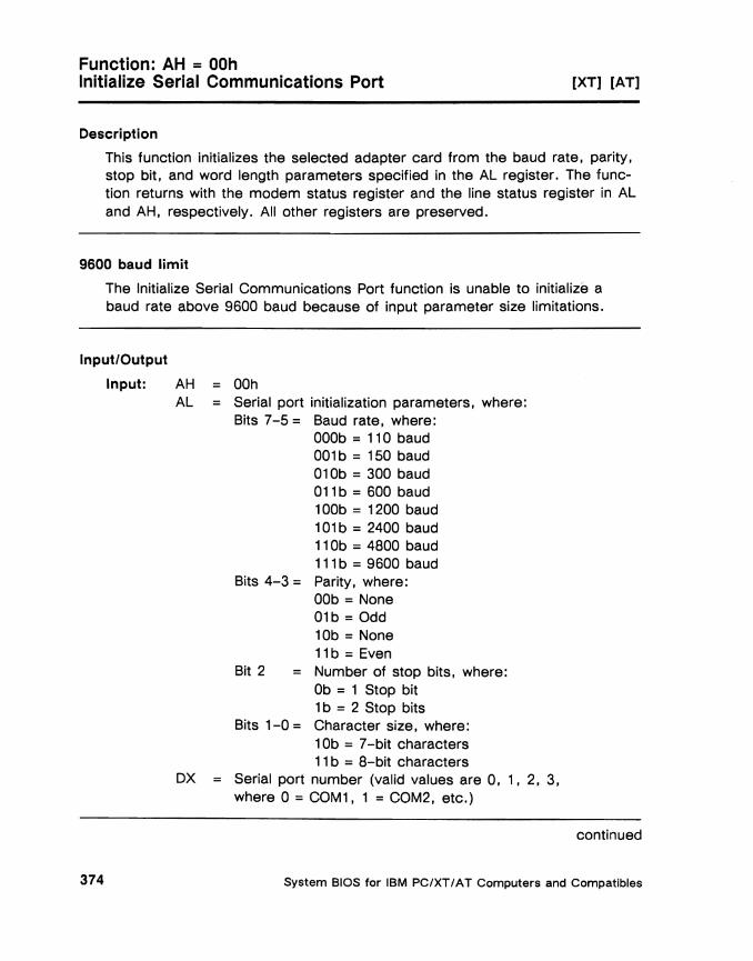
Function: AH = OOh Initialize Serial Communications Port [XT] [AT]
Description
This function initializes the selected adapter card from the baud rate, parity, stop bit, and word length parameters specified in the AL register. The function returns with the modem status register and the line status register in AL and AH, respectively. All other registers are preserved.
9600 baud limit
The Initialize Serial Communications Port function is unable to initialize a baud rate above 9600 baud because of input parameter size limitations.
Input/Output
Input: AH = OOh AL = Serial port initialization parameters, where:
Bits 7-5 = Baud rate, where: OOOb = 110 baud 001b = 150 baud 010b = 300 baud 011b = 600 baud 100b = 1200 baud 101 b = 2400 baud 11 Ob = 4800 baud 111b = 9600 baud
Bits 4-3 = Parity, where: OOb = None 01b = Odd 10b = None 11b = Even
Bit 2 Number of stop bits, where: Ob = 1 Stop bit 1 b = 2 Stop bits
Bits 1-0 = Character size, where: 1Ob = 7-bit characters 11 b = 8-bit characters
DX Serial port number (valid values are 0, 1, 2, 3, where 0 = COM1, 1 = COM2, etc.)
continued
System BIOS for IBM PC/XT/AT Computers and Compatibles 374

Function: AH = OOh Initialize Serial Communications Port, Continued [XT] [AT]
Input/Output, cont' d
Output: AH = Line Status, where: Bit 7 = 1 Time-out error Bit 6 = 1 Transmitter shift and holding register empty Bit 5 = 1 Transmitter holding register empty Bit 4 = 1 Break interrupt Bit 3 = 1 Framing error Bit 2 = 1 Parity error Bit 1 = 1 Overrun error Bit 0 = 1 Data ready
AL = Modem Status, where: Bit 7 = 1 Data carrier detect Bit 6 = 1 Ring indicator Bit 5 = 1 Data set ready Bit 4 = 1 Clear to send Bit 3 = 1 Delta data carrier select Bit 2 = 1 Trailing edge ring indicator Bit 1 = 1 Delta data set ready Bit 0 = 1 Delta clear to send
INT 14h Serial Communications Service 375
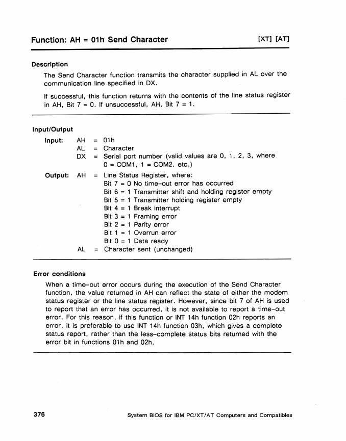
[XT] [AT] Function: AH = 01 h Send Character
Description
The Send Character function transmits the character supplied in AL over the communication line specified in OX.
If successful, this function returns with the contents of the line status register in AH, Bit 7 = O. If unsuccessful, AH, Bit 7 = 1.
Input/Output
Input: AH = 01h AL Character OX - Serial port number (valid values are 0, 1, 2, 3, where
o = COM1, 1 = COM2, etc.)
Output: AH Line Status Register, where: Bit 7 = 0 No time-out error has occurred Bit 6 = 1 Transmitter shift and holding register empty Bit 5 = 1 Transmitter holding register empty Bit 4 = 1 Break interrupt Bit 3 = 1 Framing error Bit 2 = 1 Parity error Bit 1 = 1 Overrun error Bit 0 = 1 Data ready
AL Character sent (unchanged)
Error conditions
When a time-out error occurs during the execution of the Send Character function, the value returned in AH can reflect the state of either the modem status register or the line status register. However, since bit 7 of AH is used to report that an error has occurred, it is not available to report a time-out error. For this reason, if this function or INT 14h function 02h reports an error, it is preferable to use INT 14h function 03h, which gives a complete status report, rather than the less-complete status bits returned with the error bit in functions 01 hand 02h.
System BIOS for IBM PC/XT/AT Computers and Compatibles 376

Function: AH = 02h Receive Character [XT] [AT]
Description
The Receive ·Character function receives one character from the serial port specified in the OX register.
If successful. this function returns with the character received in the AL register. The contents of the line status register is returned in the AH register.
Input/Output
Input: AH = 02h OX Serial port number (valid values are O. 1. 2. 3.
where 0 = COM1. 1 = COM2. etc.)
Output: AH = Line Status Register. where: Bit 7 = 0 No time-out error has occurred Bit 6 = 1 Transmitter shift and holding register empty Bit 5 = 1 Transmitter holding register empty Bit 4 = 1 Break interrupt Bit 3 = 1 Framing error Bit 2 = 1 Parity error Bit 1 = 1 Overrun error Bit 0 = 1 Data ready
AL = Character received
Error conditions
If a time-out error occurs during the execution of the Receive Character function. the value returned in AH can reflect the state of either the modem status register or the line status register. However. since bit 7 of AH is used to report that an error has occurred. it is not available to report a time-out error. For this reason. if this function or INT 14h function 01 h reports an error. it is preferable to use INT 14h function 03h. which gives a complete status report. rather than the less-complete status bits returned with the error bit in functions 01 hand 02h.
INT 14h Serial Communications Service 377
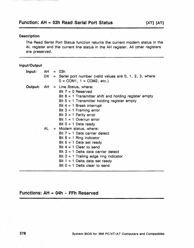
Function: AH = 03h Read Serial Port Status [XT] [AT]
Description
The Read Serial Port Status function returns the current modem status in the AL register and the current line status in the AH register. All other registers are preserved.
Input/Output
Input: AH = 03h DX = Serial port number (valid values are 0, 1 j 2, 3, where
o = COM1, 1 = COM2, etc.)
Output: AH = Line Status, where: Bit 7 = 0 Reserved Bit 6 = 1 Transmitter shift and holding register empty Bit 5 = 1 Transmitter holding register empty Bit 4 = 1 Break interrupt Bit 3 = 1 Framing error Bit 2 = 1 Parity error Bit 1 = 1 Overrun error Bit 0 = 1 Data ready
AL = Modem status, where: Bit 7 = 1 Data carrier detect Bit 6 = 1 Ring indicator Bit 5 = 1 Data set ready Bit 4 = 1 Clear to send Bit 3 = 1 Delta data carrier detect Bit 2 = 1 Trailing edge ring indicator Bit 1 = 1 Delta data set ready Bit 0 = 1 Delta clear to send
Functions: AH = 04h - FFh Reserved
System BIOS for IBM PC/XTIA T Computers and Compatibles 378
Chapter 13
INT 15h System Services
Overview
Introduction
INT 15h. System Services. provides several services:
• Multitasking hooks The BIOS provides six hooks for use by multitasking operating systems. In a DOS environment (which is not a multitasking operating system) these six functions do nothing except return to the caller. A multitasking operating system would normally intercept these function calls by replacing the INT 15h vector and processing these function calls itself.
• Joystick support Function 84h supports up to two joysticks. Function 84h has two subfunctions: read current switch settings and read resistive inputs.
• Wait routines INT 15h provides two wait functions: Function 83h. Set Event Wait Interval. and Function 86h. Wait. Function 86h does not return control to the caller until a specified interval is completed. Function 83h returns control to the caller immediately but sets a bit when a predetermined interval is over.
continued
INT 15h System Services 379

Overview, Continued
Introduction, cont'd
• Protected mode support The BIOS System Services provides limited protected mode support through two functions: Function 87h, Move Block, and Function 89h, Switch Processor to Protected Mode.
• System information Function COh, Return System Configuration Parameters, and Function 88h, Read Extended Memory Size, provide information about the system.
How INT 15h services are invoked
INT 15h invokes the BIOS System Services.
The INT 15h vector resides at interrupt table address 00: 54h. The BIOS initializes the INT 15h vector to FOOO:F859h.
Individual INT 15h System Services functions are selected via the AH register. Subfunctions are selected via the AL, OX, or BH registers.
In this chapter
The following topics are discussed in the rest of the INT 15h System Services chapter:
• Summary of Functions
• Hardware Environment
• System RAM Data
• CMOS RAM Data
• ROM BIOS Data
• System Services lID Ports
• System Services Functions
System BIOS for IBM PC/XTIAT Computers and Compatibles 380

Summary of Functions
Summary of INT 15h System Services functions
The table below lists the System Services functions and subfunctions.
Functions AH = 80h. 81 h. 82h. 85h. 90h. and 91 h (i. e .• those marked with an asterisk in the table below) are multitasking hooks. A multitasking operating system would normally intercept these function calls by replacing the INT 15h vector and processing these function calls itself. In DOS (which is not a multitasking operating system) these six functions do nothing except return immediately to the caller with the Carry Flag cleared.
Function Description Platforms
OOh Turn Cassette Motor On [PC]
01h Turn Cassette Motor Off [PC]
02h Read Cassette [PC]
03h Write to Cassette [PC]
4Fh Keyboard Intercept [AT]
80h Device Open' [AT]
81h Device Close' [AT]
82h Program Termination' [AT]
83h Set Event Walt Interval [AT]
AL =OOh Set Walt AL =01h Cancel Wait
84h Joystick Support [AT] DX =OOh Read Current Switch Settings DX =01h Read Resistive Inputs
85h System Request Key' [AT]
8Sh Walt [AT]
87h Move Block [AT]
88h Read Extended Memory Size [AT]
89h Switch Processor to Protected Mode [AT]
90h Device Busy' [AT]
91h Interrupt Complete' [AT]
COh Return System Configuration Parameters [AT)
• Multitasking hooks
INT 15h System Services 381
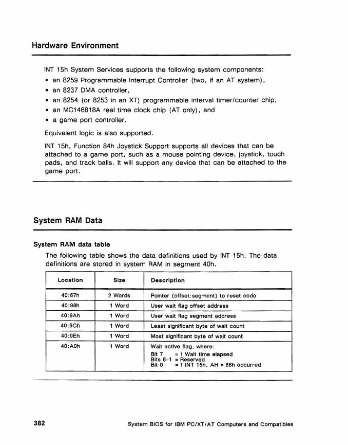
Hardware Environment
INT 15h System Services supports the following system components:
• an 8259 Programmable Interrupt Controller (two. if an AT system).
• an 8237 DMA controller.
• an 8254 (or 8253 in an XT) programmable interval timer/counter chip.
• an MC146818A real time clock chip (AT only). and
• a game port controller.
Equivalent logic is also supported.
INT 15h. Function 84h Joystick Support supports all devices that can be attached to a game port. such as a mouse pointing device, joystick, touch pads, and track balls. It will support any device that can be attached to the game port.
System RAM Data
System RAM data table
The following table shows the data definitions used by INT 15h. The data definitions are stored in system RAM in segment 40h.
Location Size Description
40:67h 2 Words Pointer (offset:segment) to reset code
40:98h 1 Word User walt flag offset address
40:9Ah 1 Word User walt flag segment address
40:9Ch 1 Word Least significant byte of wait count
40:9Eh 1 Word Most significant byte of wait count
40:AOh 1 Word Wait active flag. where: Bit 7 =1 Wait time elapsed Bits 6-1 =Reserved Bit 0 = liNT 15h. AH =86h occurred
System BIOS for IBM PC/XT/AT Computers and Compatibles 382
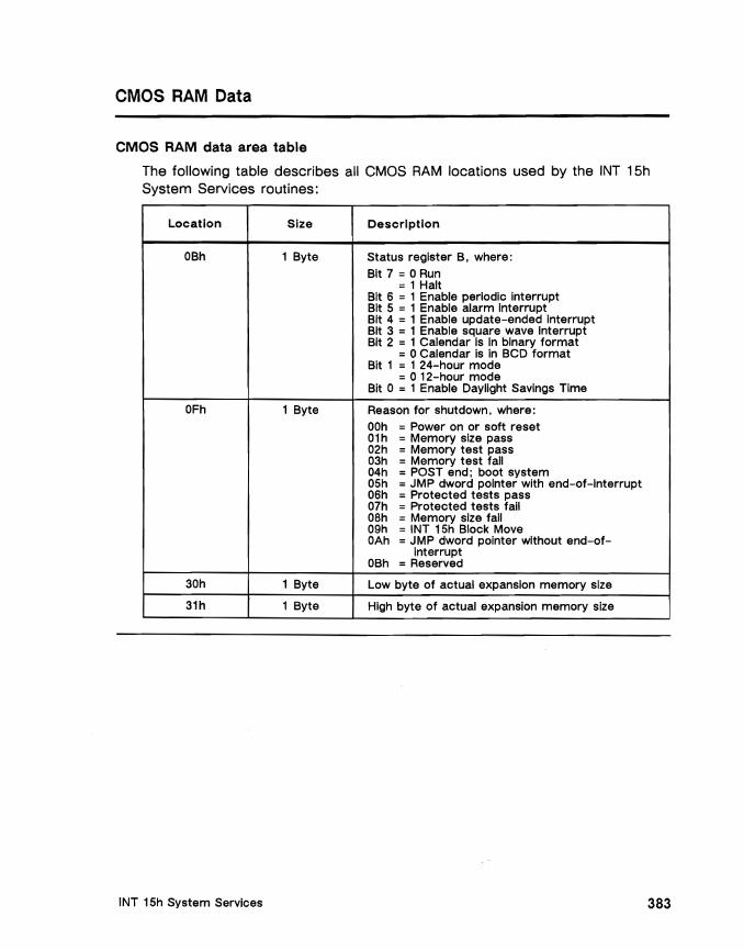
CMOS RAM Data
CMOS RAM data area table
The following table describes all CMOS RAM locations used by the INT 15h System Services routines:
Location Size
OBh 1 Byte
OFh 1 Byte
30h 1 Byte
31h 1 Byte
Description
Status register B, where:
Bit 7 =0 Run =1 Halt
Bit 6 =1 Enable periodic Interrupt Bit S =1 Enable alarm Interrupt Bit 4 =1 Enable update-ended interrlJpt Bit 3 =1 Enable square wave Interrupt Bit 2 =1 Calendar is in binary format
=0 Calendar is in BCD format Bit 1 =1 24-hour mode
=0 12-hour mode Bit 0 =1 Enable Daylight Savings Time
Reason for shutdown, where: OOh = Power on or soft reset 01h =Memory size pass 02h =Memory test pass 03h =Memory test fall 04h =POST end; boot system OSh =JMP dword pointer with end-of-interrupt 06h =Protected tests pass 07h = Protected tests fall 08h =Memory size fall 09h =INT 1Sh Block Move OAh =JMP dword pointer without end-of
interrupt OBh = Reserved
Low byte of actual expansion memory size
High byte of actual expansion memory size
INT 1Sh System Services 383
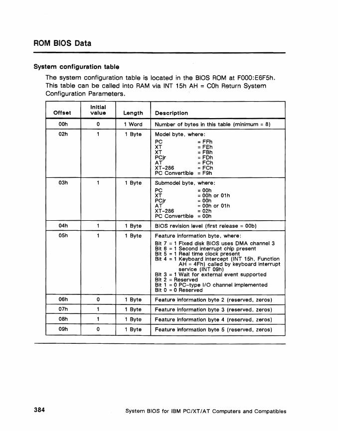
ROM BIOS Data
System configuration table
The system configuration table is located in the BIOS ROM at FOOO:E6F5h. This table can be called into RAM via INT 15h AH = COh Return System Configuration Parameters.
Initial Offset value Length Description
OOh 0 1 Word Number of bytes In this table (minimum =8)
02h 1 1 Byte Model byte, where: PC = FFh XT =FEh XT =FBh PCjr =FDh AT =FCh XT-286 =FCh PC Convertible =F9h
03h 1 1 Byte Submodel byte, where: PC =OOh XT =OOh or 01h PCjr =OOh AT =OOh or 01h XT-286 =02h PC Convertible =OOh
04h 1 1 Byte BIOS revision level (first release = OOb)
05h 1 1 Byte Feature information byte, where: Bit 7 =1 Fixed disk BIOS uses DMA channel 3 Bit 6 =1 Second Interrupt chip present Bit 5 =1 Real time clock present Bit 4 =1 Keyboard intercept (INT 15h, Function
AH =4Fh) called by keyboard interrupt service (INT 09h)
Bit 3 =1 Wait for external event supported Bit 2 =Reserved Bit 1 =0 PC-type I/O channel implemented Bit 0 =0 Reserved
06h 0 1 Byte Feature Information byte 2 (reserved, zeros)
07h 1 1 Byte Feature information byte 3 (reserved, zeros)
08h 1 1 Byte Feature Information byte 4 (reserved, zeros)
09h 0 1 Byte Feature information byte 5 (reserved, zeros)
System BIOS for IBM PC/XT/AT Computers and Compatibles 384

System Services 1/0 Ports
Read/Write I/O Address Status Description
0020h W PIC, Initialization Command Word 1 (ICW1) (Bit 4 is one), where:
Bits 7-5 =0 Only used in 80/85 mode Bit 4 =1 Reserved Bit 3 =0 Reserved Bit 2
Bit 1
=0 Successive Interrupt vectors are separated by eight bytes
=1 Successive Interrupt vectors are separated by four bytes
=0 Cascade mode
Bit 0 =1 Single mode - no ICW3 needed =0 No ICW4 needed =1 ICW4 needed
0021h W PIC, ICW2, ICW3, or ICW4 in sequential order after ICW1 written to Port 0020h
ICW2, where: Bits 7-3 =Address lines AO-A3 of base vector
address for interrupt controller Bits 2-0 =0 Reserved
ICW3, where: Bits 7-0 =0 Slave controller not attached to
corresponding Interrupt pin =0 Slave controller attached to
corresponding Interrupt pin
ICW4, where:
Bits 7-5 =0 Reserved Bit 4 =0 No special fully-nested mode
Bits 3-2 =1 Special fully-nested mode =OOb Non-buffered mode =01 b Non-buffered mode
Bit 1
=10b Buffered mode/slave =11b Buffered mode/master =0 Normal EOI =1 Auto EOI
Bit 0 =0 80/85 mode =1 8086/8088 mode
0021h R/W PIC, Interrupt mask register (OCW1), where: Bit 7 =0 Enable parallel printer interrupt Bit 6 Bit 5 Bit 4 Bit 3 Bit 2 Bit 1 Bit 0
=0 Enable diskette Interrupt =0 Enable fixed disk Interrupt =0 Enable serial port 1 Interrupt =0 Enable serial port 2 interrupt =0 Enable video Interrupt =0 Enable keyboard Interrupt=0 Enable timer interrupt
continued
INT 15h System Services 385
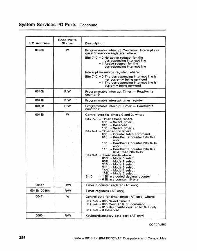
System Services 1/0 Ports, Continued
Read/Write I/O Address Status Description
0020h W Programmable Interrupt Controller, Interrupt requestlln-service registers. where: Bits 7-0 = 0 No active request for the
corresponding interrupt line = 1 Active request for the
corresponding interrupt line
interrupt In-service register. where: Bits 7-0 = 0 The corresponding interrupt line is
not currently being serviced =1 The corresponding Interrupt line is
currently being serviced
0040h R/W Programmable Interrupt Timer - Read/write counter 0
0041h R/W Programmable interrupt timer register
0042h R/W Programmable Interrupt Timer - Read/write counter 2
0043h W Control byte for timers 0 and 2, where: Bits 7-6 = Timer select. where
OOb =Select timer 0 01b = Reserved 10b = Select timer 2
Bits 5-4 = Timer action where: OOb =Counter latch command 01b = Read/write counter bits 0-7
only 10b = Read/write counter bits 8-15
only 11 b = Read/write counter bits 0-7
first. then bits 8-15 Bits 3-1 = Timer mode where
OOOb =Mode 0 select 001 b = Mode 1 select X10b = Mode 2 select X11b =Mode 3 select 100b =Mode 4 select 101b =Mode 5 select
Bit 0 = 1 Binary coded decimal counter =0 Binary counter 16 bits
0044h R/W Timer 3 counter register (AT only)
0045h-0046h R/W Timer registers (AT only)
0047h W Control byte for timer three (AT only) where: Bits 7-6 =OOb Select timer 3 Bits 5-4 =OOb Counter latch command
=01 b Read/write counter bit 0-7 only Bits 3-0 =0 Reserved
0060h R/W Keyboard/auxiliary data port (AT only)
continued
System BIOS for IBM PC/XT/AT Computers and Compatibles 386
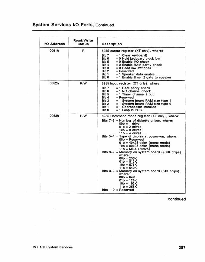
System Services 1/0 Ports, Continued
Read/Write 110 Address Status
0061h R
0062h R/W
0063h R/W
Description
8255 output register (XT only), where:
Bit 7 =1 Clear keyboard) Bit 6 =0 Hold keyboard clock low Bit 5 =0 Enable 110 check Bit 4 =0 Enable RAM parity check Bit 3 =0 Read low switches Bit 2 =Reserved Bit 1 =1 Speaker data enable Bit 0 =1 Enable timer 2 gate to speaker
8255 Input register (XT only), where: Bit 7 =1 RAM parity check Bit 6 =1 110 channel check Bit 5 =1 Timer channel 2 out Bit 4 =Reserved Bit 3 =1 System board RAM size type 1 Bit 2 =1 System board RAM size type 0 Bit 1 =1 Coprocessor installed Bit 0 =1 Loop in POST
8255 Command mode register (XT only), where: Bits 7-6
Bits 5-4
Bits 3-2
Bits 3-2
Bits 1-0
=Number of diskette drives, where: OOb =1 drive 01 b =2 drives 1Ob =3 drives llb =4 drives
=Type of display at power-on, where: OOb = Reserved 01b =40x25 color (mono mode) lOb =80x25 color (mono mode) llb = MDA (80x25)
=Memory on system board (256K chips), where: OOb =256K 01b =512K lOb =576K l1b =640K
=Memory on system board (64K chips), where: OOb =64K 01b = 128K lOb = 192K 11 b =256K
=Reserved
continued
INT 15h System Services 387
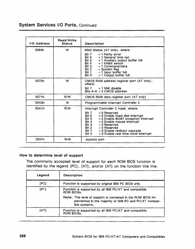
System Services 1/0 Ports, Continued
ReadlWrlte 1/0 Address Status Description
0064h W 8042 Status (AT only), where: Bit 7 =1 Parity error Bit 6 =1 General time out Bit 5 = 1 Auxiliary output buffer full Bit 4 =1 Inhibit switch Bit 3 =1 Command/data Bit 2 =System flag Bit 1 =1 Input buffer full Bit 0 =1 Output buffer full
0070h W CMOS RAM address register port (AT only) , where: Bit 7 =1 NMI disable Bits 6-0 =0 CMOS address
0071h R/W CMOS RAM data register port (AT only)
OOAOh W Programmable Interrupt Controller 2
00A1h R/W Interrupt Controller 2 mask, where: Bit 7 =0 Reserved Bit 6 =0 Enable fixed disk interrupt Bit 5 =0 Enable 80387 exception interrupt Bit 4 =0 Enable mouse interrupt Bit 3 =0 Reserved Bit 2 =0 Reserved Bit 1 =0 Enable redirect cascade Bit 0 =0 Enable real time clock interrupt
0201h R/W Joystick port
How to determine level of support
The commonly accepted level of support for each ROM 810S function is identified by the legend [PC], [XT] , and/or [AT] on the function title line.
Legend Description
[PC] Function is supported by original IBM PC BIOS only.
[XTI Function Is supported by all IBM PC/XT and compatible ROM BlOSs.
Note: This level of support is contained in the ROM BIOS implemented in the majority of IBM PC and PC/XT compatible systems.
[AT] Function is supported by all IBM PC/AT and compatible ROM BlOSs.
System BiOS for IBM PC/XT/AT Computers and Compatibles 388

Function: AH = OOh Turn Cassette Motor On [PC]
Description
Older PC BlOSs support the Turn Cassette Motor On function. On an older PC, this function turns on the tape cassette motor if a cassette drive is attached to the system. The cassette connector is generally located near the keyboard connector on the back of the PC.
XT and AT BlOSs support this function to the extent that the BIOS does not generate an error and returns with registers preserved if this function is invoked.
Functions OOh, 01 h, 02h, and 03h may be useful to those who need to attach a low-voltage analog device to a PC or to generate a signal to a signalling device. These functions control the operation of a relay within the PC. This relay is useful for controlling low-voltage and low-current devices.
Input/Output
Input: AH = OOh
Output: AH = OOh No error 86h Cassette not present.
= Status CF o No error
= 1 Error
INT 15h System Services 389
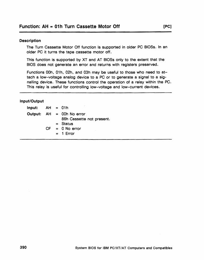
Function: AH = 01h Turn Cassette Motor Off [PC]
Description
The Turn Cassette Motor Off function is supported in older PC BlOSs. In an older PC it turns the tape cassette motor off.
This function is supported by XT and AT BlOSs only to the extent that the BIOS does not generate an error and returns with registers preserved.
Functions OOh, 01h, 02h, and 03h may be useful to those who need to attach a low-voltage analog device to a PC or to generate a signal to a signalling device. These functions control the operation of a relay within the PC. This relay is useful for controlling low-voltage and low-current devices.
Input/Output
Input: AH = 01 h
Output: AH = OOh No error 8Sh Cassette not present.
= Status CF = a No error
= 1 Error
System BIOS for IBM PC/XT I AT Computers and Compatibles 390
Function: AH = 02h Read Cassette [PC]
Description
The Read Cassette function is supported in older PCs. Invoking this function causes the system to read data from the cassette.
This function is supported for compatability purposes only on XT and AT systems. An XT or AT BIOS preserves register values, does not generate an error, and returns to the caller when this function is invoked.
Input/Output
Input: AH 02h CX = Number of bytes to read ES:BX = Segment:Offset of buffer
Output: AH = OOh No error 01 h CRC error
= 02h Bit signals scrambled = 04h No data found
SOh Invalid command = S6h Cassette not present = Status
CF = 0 No error = 1 Error
DX Number of bytes actually read EX:BX = Segment:Offset + 1 of last byte read
INT 15h System Services 391

Function: AH = 03h Write to Cassette [PC]
Description
The Write to Cassette function is supported in older PCs. Invoking this function causes the system to write data from the system to the cassette.
This function is supported for compatability purposes only on XT and AT systems. An XT or AT BIOS preserves register values, does not generate an error, and returns to the caller when this function is invoked.
InputfOutput
Input: AH = 03h CX = Number of bytes to read ES:BX = Segment:Offset of buffer
Output: AH = OOh No error BOh Invalid command 86h Cassette not present Status
CF 0 No error = 1 Error
CX OOH EX:BX = Segment:Offset + 1 of last byte written
System BIOS for IBM PC/XT / AT Computers and Compatibles 392
Function: AH = 4Fh Keyboard Intercept [XT] [AT]
Description
The INT 09h ISR calls this function, each time a key is pressed.
This function can be used to create alternate keyboard layouts and/or to cause the system to ignore certain keystrokes. For example, an operating system or resident utility can intercept Function 4Fh to filter the raw keyboard data stream. A new handler can be written to substitute a different scan code, return the existing scan code, or discard the scan code altogether before returning to the caller.
If this function is not intercepted by an alternate routine, the BIOS returns to the caller with the scan code in AL (unchanged) and the Carry Flag clear. Otherwise, it processes as described below.
Input/Output
Input: AH AL =
4Fh Scan code input by INT 09h ISR
Output: AL CF
=
Scan code o Keystroke unchanged (original scan code in AL) 1 Keystroke changed (new scan code in AL)
Note: This function is supported only by later versions of the XT and AT BIOS. To determine if your BIOS supports this function, invoke INT 15h AH = COh Return System Configuration Parameters. If the Keyboard Intercept function is supported, bit 4 of feature information byte 1 (40:05h) will be set to 1.
INT 15h System Services 393

Function: AH = SOh Device Open [AT]
Description
This function is used by multitasking operating systems. A multitasking operating system would intercept this function and process the request as necessary. Normally. the BIOS simply returns with AH set to OOh and the Carry Flag clear. The caller must clear the Carry Flag before invoking this function.
A multitasking operating system could use this function to capture control of a logical device so as to arbitrate its use by multiple processes.
Input/Output
Input: AH = aOh BX = Device ID CF = 0 CX = Process ID
Output: AX OOaOh
System BIOS for IBM PC/XT IA T Computers and Compatibles 394
Function: AH = 81h Device Close [AT]
Description
This function is used by multitasking operating systems. A multitasking operating system would intercept this function and process the request as necessary. Normally, the BIOS simply returns with AH set to OOh and the Carry Flag clear. The caller must clear the Carry Flag before invoking this function.
This function could be used by a multitasking operating system to release control of a logical device for a process. See also INT 15h, AH = 80h and 82h.
Input/Output
Input: AH = 81h BX = Device ID CF = 0 CX = Process ID
Output: AX = 0081h
INT 15h System Services 395
Function: AH = 82h Program Termination [AT]
Description
This function is used by multitasking operating systems. A multitasking operating system would intercept this function and process the request as necessary. Normally, the BIOS simply returns with AH set to OOh and the Carry Flag clear. The caller must clear the Carry Flag before invoking this function.
A multitasking operating system could use this function to release control of all logical device"s for a process that will soon terminate. See also INT 15h, AH = 80h and 81 h.
Input/Output
Input: AH = 82h BX = Device 10 CF = 0
Output: AX = 0082h
System BIOS for IBM PC/XTI AT Computers and Compatibles 396

Function: AH = 83h Set Event Wait Interval [AT]
Description
INT 15h provides two wait functions: Function 83h Set Event Wait Interval and Function 86h Wait. The difference between these two functions is that processing continues when INT 15h Function 83h is invoked, but processing stops for the calling program when INT15h Function 86h is invoked.
Function 83h, subfunction AL = OOh causes the BIOS to set a signal in a user-defined memory location after a specified interval passes. Function 83h, subfunction AL = 01 h cancels the wait.
This function accesses INT 70h, the Real Time Clock ISR. INT 70h has two components: an alarm interrupt service, and a periodic interrupt service. INT 15h, Function 83h sets and cancels the periodic interrupt service of INT 70h, as does INT 15h, Function 86h.
With this function, the caller must specify a location in ES:BX where the BIOS will set the high-order bit when the time period specified in CX and OX expires. The caller is responsible for clearing this bit after the time interval expires and before invoking this function again.
The input and output register settings are shown on the following page.
Additional Information
• An event wait's duration is an integral multiple of 976 microseconds, since the MC146818 RTC chip is usually programmed to tick 1024 times per second, or once every 976 microseconds.
• This function provides hardware-independent wait periods of finer granularity than provided with the DOS Get Time Function (INT 21h, Function 2Ch), or the INT 08h System Timer ISR, which ticks only 18.2 times per second. MS-DOS INT 21 h, Function 2Ch returns time only in hundredths of a second.
continued
INT 15h System Services 397
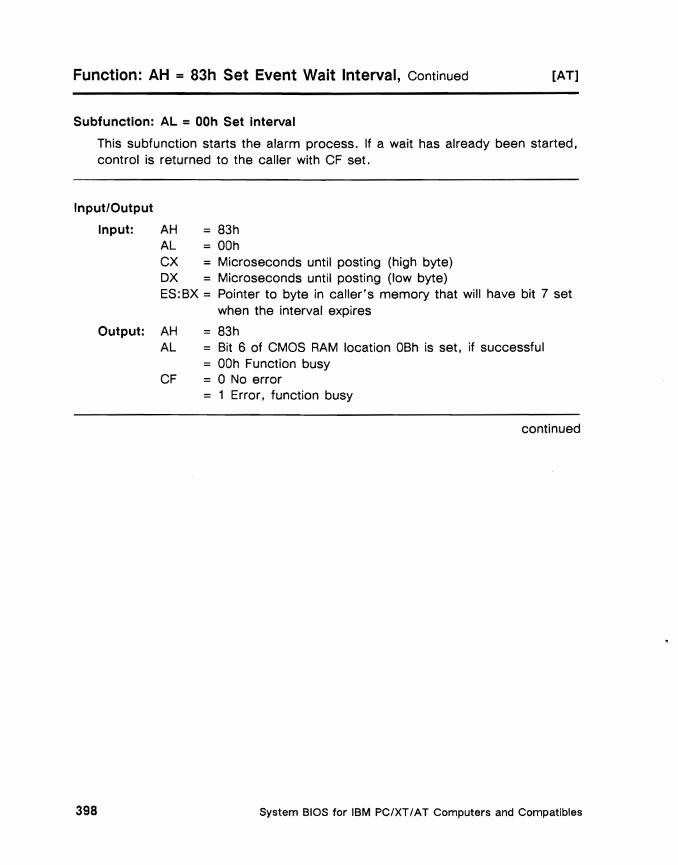
Function: AH = 83h Set Event Wait Interval, Continued [AT]
Subfunction: AL = OOh Set interval
This subfunction starts the alarm process. If a wait has already been started, control is returned to the caller with CF set.
Input/Output
Input: AH == 83h AL OOh CX == Microseconds until posting (high byte) ox == Microseconds until posting (low byte) ES:BX == Pointer to byte in caller's memory that will have bit 7 set
when the interval expires
Output: AH 83h AL == Bit 6 of CMOS RAM location OBh is set, if successful
== OOh Function busy CF == 0 No error
== 1 Error, function busy
continued
System BIOS for IBM PC/XT I AT Computers and Compatibles 398

Function: AH = B3h Set Event Wait Interval, Continued [AT]
Subfunction: AL = 01 h Cancel interval
This function cancels the interval in progress.
Input/Output
Input: AH = 83h AL = 01h
Output: AX = 8300h CF = 0 No error
1 Error
Error conditions
No action is taken and the registers are preserved if CX and DX contain zero values. If a wait is already in progress, CF is set and control is returned to the caller.
If the subfunction code in AL is not OOh or 01 h, one (1) is subtracted from AL, the Carry Flag is set, and control is returned to the caller.
Reference
Refer to Chapter 15, INT 1Ah Time-ot-Day Service, tor more information about INT 15h, Functions 83h and 86h.
INT 15h System Services 399

Function: AH = 84h Joystick Support [AT]
Description
This function controls a joystick connected to the game control adapter. It has two subfunctions: read current joystick switch settings and read resistive inputs. which are described below.
Subfunction: DX = OOh Read current switch settings
This subfunction returns the switch settings read from the joystick in bits 4 through 7 of AL. while bits 3-0 of AL are cleared. The switch settings are read at port 0201 h. If no game adapter is installed. AL is cleared.
Input/Output
Input: AH OX
= 84h OOh
Output: AH AL CF
=
=
OH on entry to this function Switch settings in bits 7-4. bits 3-0 = OOOOb o No error 1 Incorrect value in OX
continued
System BIOS for IBM PC/XT/AT Computers and Compatibles 400

Function: AH = 84h Joystick Support, Continued [AT]
Subfunction: OX = 01 h Read resistive inputs
This subfunction retrieves the relative position of the X and Y coordinates of the two possible joysticks. Control is returned to the caller and CF is cleared. If no game adapter is installed, AX, BX, CX, and OX are all cleared.
Input/Output
Input: AH OX
84h
= 01h
Output: AX BX CF
= Joystick A X-coordinate value
= Joystick A Y -coordinate value
= o No error 1 Incorrect value in OX
CX OX
= Joystick B X-coordinate value Joystick BY-coordinate value
With a 250K Ohm joystick connected, potentiometer values will be around 0-416 (0000-01 AOh) .
INT 15h System Services 401

Function: AH = 8Sh System Request Key [AT]
Description
The keyboard interrupt function is called by INT 09h when the Sys Req key is pressed. When called, this function returns to the caller with the scan code in AL (unchanged) and the Carry Flag clear.
This function is used by multitasking operating systems. A multitasking operating system would intercept this function and process the request as necessary. Normally, the BIOS simply returns with AH set to OOh and the Carry Flag clear. The caller must clear the Carry Flag before invoking this function.
Input/Output
Input: AH = 85h AL = OOh Key make
= 01 h Key break CF = a
Output: AX = 0085h CF = a No error
= 1 Invalid number in AL
System BIOS for IBM PC/XT/AT Computers and Compatibles 402

Function: AH = 8Sh Wait [AT]
Description
This function causes the BIOS to immediately suspend activity for the calling program for the amount of time specified in CX and DX. It then sets bit 7 of location 40:AOh when the specified interval is completed.
The values entered in CX and DX must be in microseconds. However, an event wait's duration will always be an integral multiple of 976 microseconds. Any value input into CX and DX will be rounded to a multiple of 976 microseconds because the RTC, which is used by this function, is usually programmed to tick 1024 times per second, or once every 976 microseconds.
INT 15h provides two wait functions: Function a3h Set Event Wait Interval and Function a6h Wait. The difference between these two functions is that processing continues when INT a3h is invoked, but processing stops for the calling programs when INT a6h is invoked.
No action is taken and the registers are preserved if CX and DX contain zero values. If a wait is already in progress, CF is set and control is returned to the caller.
Input/Output
Input: AH = a6h CX = High byte of wait interval (in microseconds) DX = Low byte of wait interval (in microseconds)
Output: AH = a6h AL = Mask written to interrupt controller 2 (if successful)
= Unmodified if function busy CF = o No error
= 1 Function busy, wait not performed
Time delay granularity
Using this function, the caller can obtain hardware-independent delays of finer granularity than provided by the MS-DOS Get Time function (INT 21 h, Function 2Ch), or the INT OSh System Timer ISR, which ticks only 1S.2 times per second. MS-DOS INT 21 h, Function 2Ch returns time only in hundredths of a second.
INT 15h System Services 403

Function: AH = 87h Move Block [AT]
Description
This function copies a block of memory for a program that operates in real address mode from anywhere in the system address space to anywhere else in the system's address space.
A program operating in real address mode can indirectly access extended memory by using this function to copy data located in a range of extended memory to conventional memory, where the program can access the data. By invoking this function, a program can also perform the reverse operation - copying data from a conventional memory range of addresses to an extended memory address range.
Types of memory
Conventional memory is located at addresses below 640K. Only this area can be accessed by DOS and DOS application programs. Extended memory is located at addresses above 1 MB, and has to be accessed by an 80286, 80386SX, or 80386 microprocessor operating in the protected address mode.
Accessing extended memory
Addresses above 1 MB must be accessed through 80286/80386/80386SX data structures called descriptors. Descriptors are organized into structures called local descriptor tables (LOT) or global descriptor tables (GOT). Programs accessing protected mode must build descriptor tables that organize access to extended memory and allow translation of 32-bit virtual addresses into corresponding 24-bit physical addresses.
Input to this function: building part of a descriptor table
The caller must help build a descriptor table before invoking this function. However, the caller need only supply the source and destination addresses of the copy, the BIOS constructs the rest of the descriptor table.
continued
System BIOS for IBM PC/XT/AT Computers and Compatibles 404
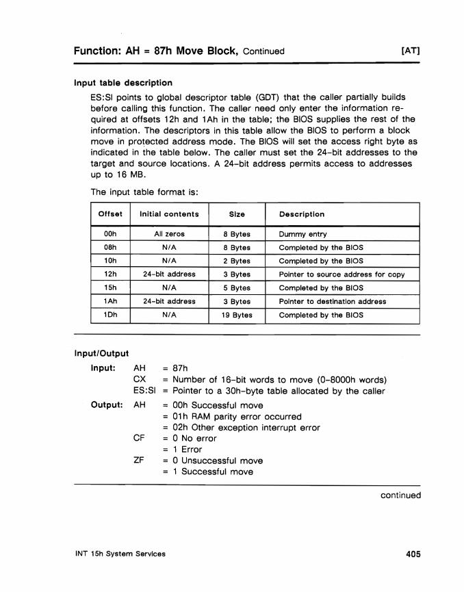
Function: AH = 87h Move Block, Continued [AT]
Input table description
ES:SI points to global descriptor table (GDT) that the caller partially builds before calling this function. The caller need only enter the information required at offsets 12h and 1 Ah in the table; the BIOS supplies the rest of the information. The descriptors in this table allow the BIOS to perform a block move in protected address mode. The BIOS will set the access right byte as indicated in the table below. The caller must set the 24-bit addresses to the target and source locations. A 24-bit address permits access to addresses up to 16 MB.
The input table format is:
Offset Initial contents Size Description
OOh All zeros 8 Bytes Dummy entry
08h N/A 8 Bytes Completed by the BIOS
10h N/A 2 Bytes Completed by the BIOS
12h 24-bit address 3 Bytes Pointer to source address for copy
15h N/A 5 Bytes Completed by the BIOS
1Ah 24-bit address 3 Bytes Pointer to destination address
1Dh N/A 19 Bytes Completed by the BIOS
Input/Output
Input: AH = 87h CX = Number of 16-bit words to move (O-BOOOh words) ES:SI = Pointer to a 30h-byte table allocated by the caller
Output: AH = OOh Successful move = 01 h RAM parity error occurred = 02h Other exception interrupt error
CF = o No error = 1 Error
ZF = o Unsuccessful move 1 Successful move
continued
INT 15h System Services 405

Function: AH = 87h Move Block, Continued [AT]
24-bit address
The 24-bit address provided by the caller is a physical base address that is the beginning address of the memory segment specified by the descriptor. This is the beginning address of the segment of code or data to be moved.
80286 descriptors
Although the caller is not concerned with this part of the table format, each 8 bytes of the table (except the first eight bytes, which must be zero) is a descriptor that references a memory segment.
Intel 80286 code forms protected mode addresses to access addresses up to 16 MB differently, using a descriptor format. The segment: offset address form is modified so that the segment address is a 24-bit address located at the descriptor starting address + 2 and the offset is a 16-bit value located at the descriptor starting address + O. The 80286 data segment descriptor format is shown in the following table. The 80386 data segment descriptor format is slightly different, but is not shown here. See the Intel 80386 Programmer's Reference for details about the 80386 protected mode instruction format.
Offset Size Description
OOh 2 Bytes The size of the memory segment minus one.
02h 3 Bytes The start address of the memory segment.
OSh 1 Byte Access flags, where: 9Ah or 9Bh =Code segment 92h or 93h = Writable data segment 90h or 91h =Read only data segment. If an 80286-based system, 9Bh, 93h, or 91h will
be the required values. . In an 80386-based system, any of the values listed above may occur.
06h 2 Bytes Reserved in an 80286 instruction
continued
System BIOS for IBM PC/XT I A T Computers and Compatibles 406
Function: AH = 87h Move Block, Continued [AT]
Interrupts disabled
Interrupts are disabled while the block move is performed. For this reason, using this function may interfere with software such as communications programs and network drivers that depend on prompt servicing of hardware interrupts.
Processor-specific information
On 80386-based systems, 32-bit moves are performed. The BIOS uses the keyboard controller to reset the processor on 80286-based systems.
Error conditions
If an exception interrupt occurs during the block move, AH is set to 02h. CF is set, ZF is cleared, and control is returned to the caller.
If a parity error occurs, AH is set to 01h, CF is set, ZF is cleared, and control is returned to the caller.
INT 15h System Services 407

Function: AH = SSh Read Extended Memory Size [AT]
Description
The Read Extended Memory Size function reads the size of the extended memory (memory beginning at address 100000h) from CMOS locations 30h and 31 h and stores the combined contents as a word in the AX register.
Extended memory is located at addresses above 1 MB, and has to be accessed by an 80286 or 80386 operating in protected mode. Since DOS is a real mode operating system, extended memory cannot be used to execute DOS programs. Extended memory can, however, be used to store data that can be indirectly accessed through an Extended Memory Manager (EMM).
The system may not be able to use the extended memory unless the system board is fully populated.
Input/Output
Input: AH = 88h
Output: AX = Number of contiguous 1 K blocks of extended memory starting at address 1024K (100000h)
System BIOS for IBM PC/XT I A T Computers and Compatibles 408

Function: AH = 89h Switch Processor to Protected Mode [AT)
Description
The Switch Processor to Protected Mode function sets the processor into protected mode and passes control to the code segment pointed to in the GOT (global descriptor table) provided by the caller.
Input/Output
Input: AH ::z:: 89h BH Index into the interrupt descriptor table (lOT) that
defines where the first 8 hardware interrupts are based BL == Index into the lOT that defines where second 8
hardware interrupts are based ES:SI Pointer to GOT built by user
Output: AH == OOh successful (CF == 0). Returns in protected mode FFh Unsuccessful
CF 0 No error 1 Error
Global descriptor table requirements
The global descriptor table (GOT) as described below defines the memory management environment that will be in effect upon return to the caller.
The entry requirements are:
• ES:SI points to a global descriptor table, which must be built before call ing this function.
• The GOT entries are used by this function to initialize the interrupt descriptor table (lOT) register, the GOT register, and the stack segment (SS) selector.
• The data Segment (OS) descriptor and the extra segment (ES) descriptor are initialized by the caller.
• BH must contain an index into the lOT to point to where the first eight hardware interrupts begin.
• BL must contain an index into the lOT to point to where the second eight hardware interrupts begin.
continued
INT 15h System Services 409
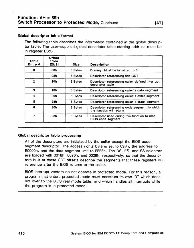
Function: AH = 89h Switch Processor to Protected Mode, Continued [AT]
Global descriptor table format
The following table describes the information contained in the global descriptor table. The user-supplied global descriptor table starting address must be in register ES:SI.
Offset Table from
Entry # ES:SI Size Description
0 OOh 8 Bytes Dummy. Must be Initialized to 0
1 08h 8 Bytes Descriptor referencing this GDT
2 10h 8 Bytes Descriptor referencing caller-defined Interrupt descriptor table
3 18h 8 Bytes Descriptor referencing caller's data segment
4 20h 8 Bytes Descriptor referencing caller's extra segment
5 28h 8 Bytes Descriptor referencing caller's stack segment
6 30h 8 Bytes Descriptor referencing code segment to which the function will return
7 38h 8 Bytes Descriptor used during this function to map BIOS code segment
Global descriptor table processing
All of the descriptors are initialized by the caller except the BIOS code segment descriptor. The access rights byte is set to 09Bh, the address to EOOOOh, and the data segment limit to FFFFh. The OS, ES, and SS selectors are loaded with 0018h, 0020h, and 0028h, respectively, so that the descriptors built at these GOT offsets describe the segments that these registers will reference after the BIOS returns to the caller.
BIOS interrupt vectors do not operate in protected mode. For this reason, a program that enters protected mode must construct its own lOT which does not overlap the BIOS real mode table, and which handles all interrupts while the program is in protected mode.
System BIOS for IBM PC/XT I AT Computers and Compatibles 410
Function: AH = 90h Device Busy [AT]
Description
This function is used by multitasking operating systems. A multitasking operating system would intercept this function and process the request as necessary. Normally, the BIOS simply returns with AH set to OOh and the Carry Flag clear. The caller must clear the Carry Flag before invoking this function.
In a multitasking operating system, this function could be invoked by the BIOS fixed disk, diskette, parallel printer, serial communications, or keyboard services to perform a programmed wait for 1/0 completion, which would allow other tasks to be dispatched while 1/0 is in progress.
Input/Output
Input: AH SOh AL Device Type, where:
OOh Fixed disk time-out = 01 h Diskette time-out = 02h Keyboard
03h Pointing device time-out 21 h Waiting for keyboard input BOh Network. FCh Fixed disk reset time-out FDh Diskette drive motor start
= FEh Printer time-out CF = 0 ES:BX = Points to a network control block (if AL = BOh or any
address above BOh)
Output: AH OOh Wait time not satisfied CF 0 Wait time not satisfied (the service must use its own
wait routine) 1 Minimum wait time satisfied (wait performed)
Device types
Serially reusable devices must be given device types 'from OOh - 7Fh; reentrant devices must have types BOh - BFh; and wait only calls, which have no corresponding function in BIOS POST, must have device types COh - FFh.
INT 15h System Services 411
Function: AH = 91 h Interrupt Complete [AT]
Description
This function is used by multitasking operating systems. A multitasking operating system would intercept this function and process the request as necessary. Normally, the BIOS simply returns with AH set to OOh and the Carry Flag clear. The caller must clear the Carry Flag before invoking this function.
In a multitasking operating system, this function could be invoked by the BIOS fixed disk, diskette, parallel printer, serial communications, or keyboard services so the service can be notified when I/O is completed. This function could also be used to allow the operating system to be informed when 1/0 is done so the requesting task could be reactivated.
The multitasking operating system printer service would not invoke this function, since printer output is not interrupt-driven.
Input/Output
Input: AH = 91h AL = Type code, where:
= OOh Disk time-out = 01 h Diskette time-out
02h Keyboard = 03h Pointing device time-out
BOh Network = FCh Fixed disk reset time-out = FDh Diskette drive motor start
CF = 0 ES:BX = Points to a network control block (if AL =BOh)
Output: None
System BIOS for IBM PC/XT I AT Computers and Compatibles 412

Function: AH = COh Return System Configuration Parameters [AT]
Description
This function returns a pointer in ES:BX to the system configuration parameter table, located in ROM at FOOO:E6F5h, which gives information about the system.
Input/Output
Input: AH = COh
Output: AH = OOh Successful = 86h System model could not be determined
CF = 0 No error (AH = OOh) = 1 System model could not be determined (AH = 86h)
ES:BX = Address of system configuration table
continued
INT 15h System Services 413

Function: AH = COh Return System Configuration Parameters, Continued [AT]
System configuration table
The system configuration table is located in the BIOS ROM at FOOO:E6F5h.
Offset Initial (hex) value Length
OOh OOh 2 Bytes
02h 02h 1 Byte
03h 03h 1 Byte
04h 04h 1 Byte
OSh OSh 1 Byte
06h 06h 1 Byte
07h 07h 1 Byte
08h 08h 1 Byte
09h 09h 1 Byte
Description
Number of bytes In this table (minimum =8)
Model byte, where: PC =FFh PC XT =FEh PC XT =FBh PCjr =FDh AT =FCh XT-286 =FCh PC Convertible =F9h Unknown system board =FFh
Sub model byte, where: PC PC XT PCjr AT AT XT-286 PC Convertible
=OOh =OOh =OOh =OOh =01h =02h =OOh
Unknown system board =FFh
BIOS revision level (first release =OOb)
Feature information byte, where: Bit 7 =1 Fixed disk BIOS uses DMA channel 3 Bit 6 =1 Second interrupt chip present Bit S =1 Real time clock present Bit 4 =1 Keyboard Intercept (INT lSh,
Function AH =4Fh) called by keyboard Interrupt service (INT 09h)
Bit 3 =1 Wait for external event supported Bit 2 =1 Extended BIOS data area is
allocated Bit 1 =0 PC-type 110 channel Implemented Bit 0 =0 Reserved
Feature Information byte 2 (reserved, zeros)
Feature Information byte 3 (reserved, zeros)
Feature Information byte 4 (reserved, zeros)
Feature Information byte S (reserved, zeros)
System BIOS for IBM PC/XT / AT Computers and Compatibles 414
Chapter 14
INT 17h Parallel Printer Service
Overview
Description
The Parallel Printer Service provides BIOS-level support for up to three parallel printer ports. This service provides three printer-related functions.
Invoking the Parallel Printer Service
Software INT 17h invokes the BIOS Parallel Printer Service.
The INT 17h vector resides at address OOSCh in the interrupt vector table. The BIOS initializes the INT 17h vector to address FOOO:EFD2h.
continued
INT 17h Parallel Printer Service 415

Overview, Continued
Summary of Parallel Printer Service functions
The following table lists the Parallel Printer functions. Individual functions are selected via the AH register.
Function Description Platforms
OOh Print Character [XT) [AT)
01h Initialize Printer [XT) [AT)
02h Read Printer Status [XT) [AT)
03h-FFh Reserved Reserved
In 'this chapter
This chapter focuses on the INT 17h Parallel Printer Service. The following topics are discussed:
• Theory of Operation
• System RAM Data
• Parallel Printer I/O Ports
• Error Handling
• Parallel Printer Functions
How to determine level of support
Throughout this book, the commonly accepted level of support for each ROM BIOS function is identified by the legend [PC], [XT] , and/or [AT] on the same line as the function title.
Legend Description
[PC) Function Is supported by original IBM PC BIOS only.
[XT) Function is supported by all IBM PC/XT and compatible ROM BlOSs.
Note: This level of support is contained in the ROM BIOS implemented in the majority of IBM PC and PC/XT compatible systems.
[AT] Function is supported by all IBM PCIA T and compatible ROM BlOSs.
System BIOS for IBM PC/XT/ AT Computers and Compatibles 416

Theory of Operation
Introduction
The parallel printer port on an IBM PC, PC/XT, and PC/AT is an 8-bit-wide device that can be used to drive various IBM PC and compatible printers. The BIOS Parallel Printer Service provides support for up to three parallel printer ports.
Parallel transmission of data
In a parallel transmission connection, all the data bits of a data byte are transmitted simultaneously over the parallel printer port. Similarly, the external device (typically a parallel printer) receives all these data bits simultaneously. This is in contrast to a serial connection, where the individual bits of a data byte are transmitted sequentially, or one at a time.
Printer adapter and interface
Typically the parallel printer adapter is used to connect a printer to the parallel port interface, but any device that accepts 8 bits of parallel data can be attached.
The 25-pin parallel connector at the rear of the adapter is the interface to an attached printer. The parallel port provides various input/output signals for communication with the printer. In particular, it uses the strobe signal to write data to the printer. The parallel port I/O signals are described on the next page.
continued
INT 17h Parallel Printer Service 417

Theory of Operation, Continued
110 signals
The parallel port makes available two types of signals: control output signals which are stored in the printer control port, and status input signals which are stored in the printer status port. These signals can be read by the microprocessor to determine the success or failure of an operation. The following table describes these signals.
Input/Output Signal Name Status Description
+IRQ Enable 0 1 =An interrupt occurs when -ACK changes from true to false
+SELECT IN 0 1 =Select the printer
-INIT 0 o=Start the printer
+AUTO FEED 0 1 =The printer produces a line feed after a line has been printed
+STROBE 0 1 =Write data to the printer
-BUSY I 1 =The printer is busy and cannot print
-AGK I o=The printer received the character and is ready to accept another character
+PE I 1 =The printer is out of paper
+SELECT I 1 =The printer is selected
-ERROR I o=An error condition has occurred
continued
System BIOS for IBM PC/XT/ A T Computers and Compatibles 418

Theory of Operation, Continued
INT 17h and the parallel port
The Parallel Printer Service is invoked via software interrupt 17h. This service contains three BIOS functions that interact with the parallel port: one to print the character in AL to the printer specified in OX, one to initialize that printer, and one to read and return that printer's status.
For example, when the caller wants to send a print request to the microprocessor, INT 17h Function OOh Print Character is invoked. This writes a character to the printer specified in OX.
The INT 17h functions reference three parallel printer 1/0 ports: the data port, the printer control port, and the printer status port.
Reference: A description of the parallel printer 110 ports can be found under the heading Parallel Printer 1/0 Ports in this chapter.
INT 17h and printing data
The process whereby an INT 17h request causes data to be printed is:
1. A program places the data byte to print in AL, puts Function OOh Print Character in AH, and performs an INT 17h.
2. The BIOS transfers the data in AL to the printer port specified in OX. The port's strobe signal is then activated, causing the data to be written to the printer. Printer status information, such as .. out of paper" or .. busy, .. is returned in AH and can be read by the microprocessor to check if the operation was successful.
continued
INT 17h Parallel Printer Service 419
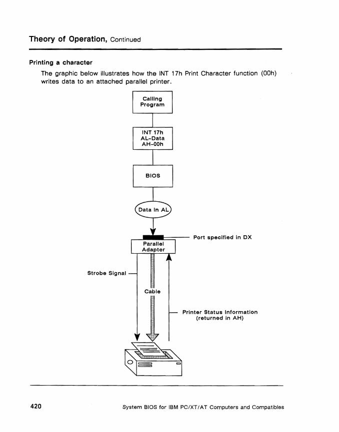
Theory of Operation, Continued
Printing a character
The graphic below illustrates how the INT 17h Print Character function (OOh) writes data to an attached parallel printer.
Calling Program
INT 17h AL-Data AH-OOh
BIOS
Port specified in DX
Strobe Signal
Cable
Printer Status Information (returned in AH)
System BIOS for IBM PC/XTI AT Computers and Compatibles 420

System RAM Data
Parallel printer data definitions
The INT 17h Para"el Printer Service uses certain locations in the BIOS data area of system RAM (address 40:00h through 40: 1 OOh). These data definitions are presented below in offset order.
Location Size Description
08h 4 words 1/0 address of up to 4 printer adapters.
10h 1 word Number of devices Installed, where: Bits 15-14 =Number of printer adapters Bits 13-12 =Reserved Bits 11-9 = Number of asynchronous adapters
(RS232) Bits 8 =Reserved Bits 7-6 = Number of diskette drives, where:
OOb = 1 diskette drive 01b =2 diskette drives
Bits 5-4 = Initial video mode, where: OOb = EGAIVGA or PGA 01b = 40x25 color 10b = 80x25 color 11 b = 80x25 black and white
Bit 3 = Reserved Bit 2 = Pointing device Bit 1 = 1 If math coprocessor Bit 0 =Diskette available for boot
78h 3 bytes One byte per adapter. Time-out values for printer number 1 through 4.
INT 17h Parallel Printer Service 421

Parallel Printer 1/0 Ports
The characteristics of each printer port are defined in thefoliowing table.
Read/Write I/O Address Status
0278h R/W
0279h R/W
027Ah R/W
0378h R/W
0379h R/W
037Ah R/W
Description
Parallel 3 data port
Parallel 3. status port, where:
Bit 7 =0 Busy Bit 6 =0 Acknowledge Bit 5 =1 Out of paper Bit 4 =1 Printer is selected Bit 3 =0 Error Bit 2 =0 IRQ has occurred Bits 1-0 =Reserved
Parallel 3, control port, where:
Bits 7-5 =Reserved Bit 4 =1 Enable IRQ Bit 3 =1 Select printer Bit 2 =0 Initialize printer Bit 1 =1 Automatic line feed Bit 0 =1 Strobe
Parallel 2 data port
Parallel 2, status port, where: Bit 7 =0 Busy Bit 6 =0 Acknowledge Bit 5 =1 Out of paper Bit 4 =1 Printer is selected Bit 3 =0 Error Bit 2 =0 IRQ has occurred Bits 1-0 =Reserved
Parallel 2, control port, where: Bits 7-5 =Reserved Bit 4 =1 Enable IRQ Bit 3 =1 Select printer Bit 2 =0 Initialize printer Bit 1 =1 Automatic line feed Bit 0 =1 Strobe
continued
System BIOS for IBM PC/XT/AT Computers and Compatibles 422

Parallel Printer 1/0 Ports, Continued
Read/Write I/O Address Status
03BCh R/W
03BDh R/W
03BEh R/W
Error Handling
Description
Parallel 1, data port
Parallel 1, status port, where:
Bit 7 Bit 6 Bit 5 Bit 4 Bit 3 Bit 2 Bits 1-0
=0 Busy =0 Acknowledge =1 Out of paper =1 Printer is selected =0 Error = 0 IRQ has occurred = Reserved
Parallel 1, control port, where:
Bits 7-5 = Reserved Bit 4 = 1 Enable IRQ Bit 3 = 1 Select printer Bit 2 = 0 Initialize printer Bit 1 = 1 Automatic line feed Bit 0 = 1 Strobe
Before entering any functions, the Parallel Printer Service ensures that the index in OX is not out of range, that the function number is not out of range, and that the printer is at the specified index.
If any of the above conditions are not met, the service returns to the caller with all registers restored except AH. When OX is out of range or the printer does not exist, AX is not modified. When the function number is out of range, AH is returned, and is decremented by 2.
INT 17h Parallel Printer Service 423

Function: AH = OOh Print Character [XT] [AT]
Description
The Print Character function prints the character in the AL register to the printer specified in the DX register. The printer status is returned in the AH register.
Input/Output
Input: AH = OOh AL Character to print DX Printer number (0 = LPT1, 1 = LPT2, or 2 = LPT3) used as
an index to the printer base port address table at 40:08h.
Output: AH Printer status, where: Bit 7 1 Printer not busy Bit 6 Acknowledgment Bit 5 = Out of paper Bit 4 = Printer selected Bit 3 1/0 error Bit 2 = Reserved Bit 1 = Reserved Bit 0 = 1 Time-out
System BIOS for IBM PC/XT/AT Computers and Compatibles 424
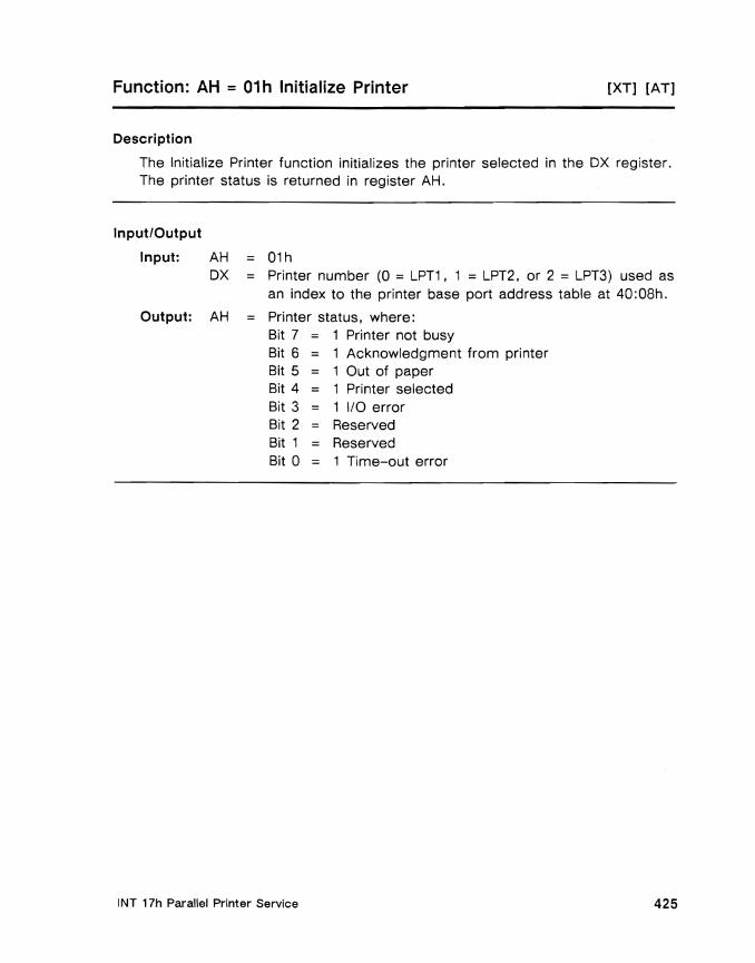
Function: AH = 01 h Initialize Printer [XT] [AT]
Description
The Initialize Printer function initializes the printer selected in the OX register. The printer status is returned in register AH.
Input/Output
Input: AH = 01 h DX = Printer number (0 = LPT1, 1 = LPT2, or 2 = LPT3) used as
an index to the printer base port address table at 40:08h.
Output: AH Printer status, where: Bit 7 1 Printer not busy Bit 6 = Acknowledgment from printer Bit 5 = Out of paper Bit 4 = Printer selected Bit 3 = 1/0 error Bit 2 Reserved Bit 1 = Reserved Bit 0 1 Time-out error
INT 17h Parallel Printer Service 425

Function: AH = 02h Read Printer Status [XT] [AT]
Description
The Read Printer Status function reads and returns the status of the printer selected by the ox register.
Input/Output
Input: AH 02h OX = Printer number (0 = LPT1, 1 = LPT2, or 2 = LPT3) used as
an index to the printer base port address table at 40: 08h.
Output: AH Printer status, where: Bit 7 1 Printer not busy Bit 6 = 1 Acknowledgment from printer Bit 5 = Out of paper Bit 4 Printer selected Bit 3 1/0 error Bit 2 = Reserved Bit 1 = Reserved Bit a = 1 Time-out error
Functions: AH = 03h - FFh Reserved
System BIOS for IBM PC/XT/AT Computers and Compatibles 426
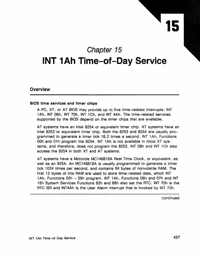
Chapter 15
INT 1Ah Time-of-Day Service
Overview
BIOS time services and timer chips
A PC. XT. or AT BIOS may provide up to five time-related interrupts: INT 1Ah. INT 08h. INT 70h. INT 1Ch. and INT 4Ah. The time-related services supported by the BIOS depend on the timer chips that are available.
AT systems have an Intel 8254 or equivalent timer chip. XT systems have an Intel 8253 or equivalent timer chip. Both the 8253 and 8254 are usually programmed to generate a timer tick 18.2 times a second. INT 1 Ah. Functions ~Oh and 01 h program the 8254. INT 1Ah is not available in most XT systems. and therefore. does not program the 8253. INT 08h and INT 1Ch also access the 8254 in both XT and AT systems.
AT systems have a Motorola MC146818A Real Time Clock. or equivalent. as well as an 8254. An MC146818A is usually programmed to generate a timer tick 1024 times per second. and contains 64 bytes of nonvolatile RAM. The first 12 bytes of this RAM are used to store time-related data. which INT 1 Ah. Functions 02h - 05h program. INT 1 Ah. Functions 06h and 07h and INT 15h System Services Functions 83h and 86h also set the RTC. INT 70h is the RTC ISR and INT4Ah is the User Alarm Interrupt that is invoked by INT 70h.
continued
INT 1Ah Time-of-Day Service 427
Overview, Continued
INT 1 Ah functions
The AT 810S Time-of-Day Service provides eight system time-related functions. One additional INT 1 Ah function is supported only by the PCjr 810S and is documented here for historical purposes.
CMOS RAM access
The Time-of-Day Service provides an easy and quick way to modify CMOS RAM data, since the first 13 bytes of CMOS RAM contain time-related information (time, day, date, alarm settings, etc). The standard method of accessing CMOS RAM involves writing information to and reading liD ports 0070h and 0071 h multiple times. Invoking an INT 1 Ah functions is much faster.
Invoking the 8105 Time-ot-Day Service
The 810S Time-of-Day Service is invoked via software interrupt INT 1 Ah. Individual Time-of-Day functions are selected via the AH register. Subfunctions are selected via the AL register.
The INT 1 Ah vector resides at address 00: 68h in the interrupt vector table. The 810S initializes the INT 1 Ah vector to address FOOO:FE6Eh.
How to determine level of support
Legend Description
[PC] Function is supported by original IBM PC BIOS only.
[XT] Function is supported by all IBM PC/XT and compatible ROM BlOSs.
Note: This level of support is contained in the ROM BIOS implemented In the majority of IBM PC and PC/XT compatible systems.
[AT] Function is supported by all IBM PC/AT and compatible ROM BlOSs.
continued
System BiOS for IBM PC/XT/AT Computers and Compatibles 428
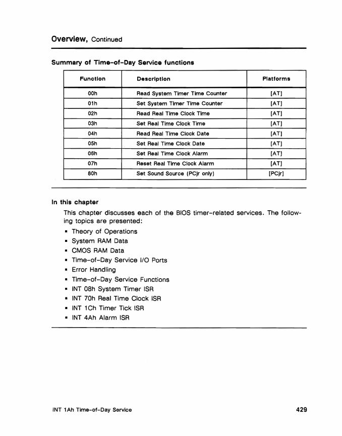
Overview, Continued
Summary of Time-of-Day Service functions
Function Description Platforms
OOh Read System Timer Time Counter [AT]
01h Set System Timer Time Counter [AT]
02h Read Real Time Clock Time [AT]
03h Set Real Time Clock Time [AT]
04h Read Real Time Clock Date [AT]
OSh Set Real Time Clock Date [AT)
06h Set Real Time Clock Alarm [AT)
07h Reset Real Time Clock Alarm [AT)
80h Set Sound Source (PCjr only) [PCjr]
In this chapter
This chapter discusses each of the BIOS timer-related services. The following topics are presented:
• Theory of Operations
• System RAM Data
• CMOS RAM Data
• Time-of-Day Service lID Ports
• Error Handling
• Time-of-Day Service Functions
• INT 08h System Timer ISR
• INT 70h Real Time Clock ISR
• INT 1 Ch Timer Tick ISR
• INT 4Ah Alarm ISR
INT 1 Ah Time-ot-Day Service 429

Theory of Operations
The BIOS provides the following timer-related support:
• INT 1Ah Time-ot-Day Service AT-only software INT 1 Ah invokes the BIOS Time-of-Day Service. The Time-of-Day Service provides access to the RTC CMOS RAM in locations OOh - OCh, and sets the INT 70h Real Time Clock ISR alarm function.
• INT OSh System Timer ISR Channel a of the Intel 8253 or 8254 Timer/Counter (or its equivalent), is usually programmed to interrupt 18.2 times per second. Each such interval generates hardware INT 08h, System Timer ISR. This interrupt is generated on PCs, XTs, and AT systems. INT 08h maintains a count of how many ticks have elapsed since midnight; this count is used for system timing purposes.
• INT 1 Ch Timer Tick ISR Software INT 08h generates INT 1Ch 18.2 times per second. The user can revector INT 1 Ch to a user-supplied routine to be executed on every system clock tick. No action is taken by the BIOS when INT 1 Ch is invoked unless this vector is modified by the caller. Any caller modifying the vector associated with this interrupt is responsible for saving and restoring all registers upon return to the BIOS. Users should return control to the BIOS through an IRET.
continued
System BIOS for IBM PC/XT /AT Computers and Compatibles 430
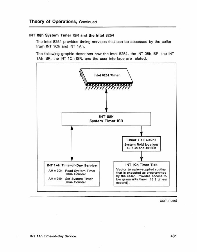
Theory of Operations, Continued
INT 08h System Timer ISR and the Intel 8254
The Intel 8254 provides timing services that can be accessed by the caller from INT 1 Ch and INT 1 Ah.
The following graphic describes how the Intel 8254, the INT 08h ISR, the INT 1Ah ISR. the INT 1Ch ISR, and the user interface are related.
Intel 8254 Timer
INT OSh System Timer ISR
Timer Tick Count
System RAM locations 4D:6Ch and 4D:6Eh
INT 1Ah Time-of-Day Service INT 1Ch Timer Tick
Vector to caller-supplied routineAH = DOh Read System Timer that Is executed as programmedTime Counter by the caller. Provides access to
AH = 01h Set System Timer low granularity timer (18.2 times/Time Counter second) .
continued
INT 1Ah Time-of-Day Service 431

Theory of Operations, Continued
• INT 70h Real Time Clock ISR The Motorola MC146818A real time clock chip, or its equivalent, is usually programmed to generate hardware interrupt 70h approximately 1024 times per second. The real time clock chip usually appears only in AT systems.
There are three functions that determine how the BIOS real time clock hardware ISR will handle interrupts from the real time clock chip.
BIOS Function Effects on BIOS RTC ISR
Periodic function These functions activate the BIOS Real Time Clock ISR's periodic interrupt component.INT 15h: AH = a3h Event Wait Interval
INT 15h: AH = a6h Wait For INT 15h AH = a3h Event Wait, the caller must provide a designated location where the BIOS will set a bit when the time for the Event Interval period is expired. For INT 15h AH = a6h Wait, the BIOS sets bit 7 of location 40:AOh after the Wait is completed.
Alarm function This function activates the BIOS Real Time Clock ISR's alarm Interrupt component.INT 1Ah: AH = 06h Set User Alarm
INT 1Ah: AH = 07h Reset User Alarm
• INT 4Ah User Alarm INT 70h generates an INT 4Ah every timer tick. Usually, INT 4Ah returns immediately to the BIOS. But a user can revector INT 4Ah to a usersupplied routine that will be executed every tick of the RTC. The user must restore registers and return to the BIOS with an IRET when the user-supplied routine completes processing.
• INT 15h System Services Functions 83h and 86h of INT 15h set the RTC ISR (INT 70h) periodic function. See Chapter 13 for a more complete description of these two functions.
continued
System BIOS for IBM PC/XTI AT Computers and Compatibles 432
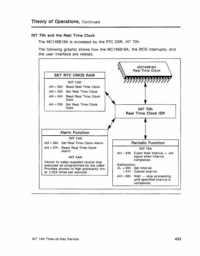
Theory of Operations, Continued
INT 70h and the Real Time Clock
The MC146818A is accessed by the RTC DSR, INT 70h.
The following graphic shows how the MC146818A, the BIOS interrupts, and the user interface are related.
SET RTC CMOS RAM
AH =02h
AH =03h
AH =04h
AH =OSh
INT 1Ah
Read Real Time Clock
Set Real Time Clock
Read Real Time Clock Date \Set Real Time Clock Date
Alarm Function
INT 1Ah
AH =06h Set Real Time Clock Alarm
AH =07h Reset Real Time Clock Alarm
INT 4Ah
Vector to caller-supplied routine that executes as programmed by the caller. Provides access to high granularity timer (1024 times per second) .
MC146818A Real Time Clock\ \
"'71'1'1', ~I'1'1' 1'1' 1'1'I'
,
INT 70h Real Time Clock ISR
,
W
Periodic Function
INT 1Sh
AH =83h Event Wait Interval - set signal when interval completed.
Subfunctlon: AL =OOh Set Interval
=01h Cancel Interval
AH =86h Wait - stop processing until specified interval is completed.
INT 1Ah Time-of-Day Service 433

System RAM Data
Description
The following table lists all system RAM data areas, beginning at segment 40h, used by the Time-of-Day Service.
Location Size Description
40:6Ch 4 Bytes 32-bit COIJnt of timer ticks since midnight
40:70h 1 Byte Timer Overflow Flag
CMOS RAM Data
Description
The Time-of-Day Service accesses the first 12 bytes of the RTC CMOS RAM data. Time data is stored in these locations. It also accesses location 32h, Century in BCD. Location 32h is updated by software access, and not internally by the chip.
The CMOS RAM configuration data definitions begin at address OEh. See Chapter 3 for a detailed description of the contents of CMOS RAM.
continued
System BIOS for IBM PC/XTI A T Computers and Compatibles 434

CMOS RAM Data, Continued
RTC CMOS RAM Data
The following table lists the MC146818A Real Time Clock data locations used by the BIOS Time-of-Day Service.
Location Size
OOh 1 Byte
01h 1 Byte
02h 1 Byte
03h 1 Byte
04h 1 Byte
OSh 1 Byte
OSh 1 Byte
07h 1 Byte
08h 1 Byte
09h 1 Byte
OAh 1 Byte
OBh 1 Byte
OCh 1 Byte
ODh 1 Byte
32h 1 Byte
Description
Current second in binary coded decimal (BCD)
Second alarm in BCD
Current minute in BCD
Minute alarm in BCD
Current hour in BCD
Hour alarm in BCD
Current day of week in BCD
Current Date in BCD
Current month In BCD
Current year in BCD
Status Register A, where:
Bit 7 =1 Update in progress Bits 6-4 =Divider that identifies the time-based
frequency Bits 3-0 =Rate-selection bits that define output
frequency and periodic Interrupt rate
Status Register B, where:
Bit 7 =0 Run =1 Halt
Bit 6 =1 Enable periodic Interrupt Bit S =1 Enable alarm Interrupt Bit 4 =1 Enable update-ended interrupt Bit 3 =1 Enable square wave interrupt Bit 2 =1 Calendar is in binary format
=0 Calendar is in BCD format Bit 1 = 1 24-hour mode
= 0 12-hour mode Bit 0 =1 Enable Daylight Savings Time
Status Register C, where:
Bits 7-4 = IRQF, PF, AF, and UF tlags, . . respectively
Bits 3-0 =Reserved
Status Register 0, where: Bit 7 = 1 Real time clock has power Bits 6-0 = Reserved
Century In BCD
INT 1Ah Time-ot-Day Service 435

Time-of-Day Service 1/0 Ports
Read/Write I/O Address Status
0020h R/W
0020h R/W
0070h W
0071h R/W
OOAOh R/W
Description
Programmable interrupt Controiier, interrupt requestlln-service registers programmed by Operation Command Word 3 (OCW3):
Interrupt request register, where:
Bits 7-0 =0 No active request for the corresponding Interrupt line
=1 Active request for the corresponding interrupt line
Interrupt In-service register, where:
Bits 7-0 =0 The corresponding interrupt line Is not currently being serviced
=1 The corresponding interrupt line is currently being serviced
PIC, Initialization Command Word 1 (ICW1) (Bit 4 is one), where:
Bits 7-5 =0 Only used in 80/85 mode Bit 4 =1 Reserved Bit 3 =0 Reserved Bit 2 =0 Successive interrupt vectors are
separated by eight bytes =1 Successive interrupt vectors are
separated by four bytes Bit 1 =0 Cascade mode
=1 Single mode - no ICW3 needed Bit 0 =0 No ICW4 needed
=1 ICW4 needed
CMOS RAM address register port, where:
Bit 7 =1 NMI disable =0 NMI enabled
Bits 6-0 =0 CMOS RAM address
CMOS RAM data port
Slave Programmable Interrupt Controiier (AT only)
System BIOS for IBM PC/XTI AT Computers and Compatibles 436

Error Handling
Description
All functions of the BIOS Time-of-Day Service set the Carry Flag if an invalid function is requested. The function number remains in AH if there is an invalid function request.
Each function handles all other errors uniquely. Refer to the description for each function for specific information about error codes.
INT 1Ah Tlme-af-Day Service 437

Function: AH = OOh Read System Timer Time Counter [AT]
Description
This function reads and returns the system tick count from the system RAM location 40:6Eh (high word) and 40:6Ch (low word). The value returned is the cumulative number of Intel 8254 clock ticks since midnight. This operation sets the timer tick count maintained by INT 08h.
The values stored in these locations are defined by the frequency of the INT 08h System Timer interrupt, which is usually programmed to interrupt approximately 18.2 ticks per second. The contents of 40:70h, the Timer Overflow Flag, are returned in AL. This value will be 0 if the timer has not exceeded 24 hours.
Interrupts are disabled while reading RAM data memory locations because a timer tick update may occur.
Execution of this function causes the Timer Overflow Flag at 40:70h to be reset to O.
Input/Output
Input: AH OOh
Output: AH = ~Oh
AL = Timer overflow value, where: = 0 Timer count is less than 24 hours since the last
power-on or system reset. Any value greater than O. The timer count is more than 24 hours since the last power-on, system reset, last system-timer time counter read, or the last time the system-timer time counter was set.
CF = 0 No error 1 Error
CX = High word of tick count DX = Low word of tick count
System BIOS for IBM PC/XT / AT Computers and Compatibles 438
Function: AH = 01h Set System Timer Time Counter [AT]
Description
This function stores values from CX and DX to RAM data areas 40:6Eh (high word) and 40:6Ch (low word). This operation sets the INT 08h timer tick count.
Execution of this function causes the Timer Overflow Flag at 40:70h to be reset to O.
Input/Output
Input: AH = 01h CX = High word of tick count DX = Low word of tick count
Output: AH OOh CF = o No error
1 Error
INT 1Ah Time-of-Day Service 439
Function: AH = 02h Read Real Time Clock Time [AT]
Description
This function first finds out if the RTC is currently updating its clock value. If so, the Carry Flag is set, the function is not performed, and control is returned to the caller.
If an update is not in progress, the appropriate values are read from the RTC CMOS RAM and returned to the caller in AL, CX, and DX, as specified below, with the Carry Flag cleared and AH = OOh.
Input/Output
Input: AH = 02h
Output: AH = OOh AL = Hours in BCD CF = 0 Clock operating
= 1 Clock not operating CH = Hours in BCD CL = Minutes in BCD DH = Seconds in BCD DL OOh - No Daylight Savings Time option
01 h - Daylight Savings Time option
System BIOS for IBM PC/XTIAT Computers and Compatibles 440
Function: AH = 03h Set Real Time Clock Time [AT]
Description
This function first finds out if the RTC is currently updating its clock value. If an update is in progress, the real time clock is initialized, the Carry Flag is set, the function is not performed, and control is returned to the caller.
The values placed by the caller in CX and DX are stored in their respective CMOS RAM storage locations. Hours are stored in CMOS RAM location 04h, minutes in location 02h, and seconds in location OOh.
Input/Output
Input: AH 03h CH Hours in BCD CL Minutes in BCD DH Seconds in BCD DL OOh No Daylight Savings Time option
01 h Daylight Savings Time option
Output: AH OOh AL Value written to CMOS OBh register CF o No error
1 Error
If a time-out occurs, which indicates that an update is in progress, the clock is initialized and the routine continues as if an update were not in progress.
INT 1 Ah Time-of-Day Service 441
Function: AH = 04h Read Real Time Clock Date [AT]
Description
This function first finds out if the RTC is currently updating its clock value. If it is, the Carry Flag is set, this function is not performed, and control is returned to the caller.
If no time-out occurs, the century, year, month, and day are extracted from CMOS RAM and are returned to the caller as described below. Upon return, the Carry Flag is cleared and AH = OOh.
Input/Output
Input: AH 04h
Output: AH = OOh CF = 0 No error
= 1 Clock update in progress CH = Century in BCD (either 19 or 20) CL = Year in BCD DH = Month in BCD DL - Day in BCD
If a time-out occurs, which indicates that an update is in progress, the Carry Flag is set, AH is cleared, and control is returned to the caller.
System BIOS for IBM PC/XTI AT Computers and Compatibles 442
Function: AH = OSh Set Real Time Clock Date [AT]
Description
This function first finds out if the RTC is currently updating its clock value. If it is, the Carry Flag is set, this function is not performed, and control is returned to the caller.
The values placed in CX and OX, as defined below, are stored in their respective CMOS RAM storage locations. Century is stored in location 32h, year in 09h, month in location OSh, and day in location 06h. This function then returns to the caller with the Carry Flag cleared and AH = OOh.
Input/Output
Input: AH = OSh CH = Century in BCD (either 19 or 20) CL = Year in BCD DH = Month in BCD DL = Day in BCD
Output: AH - OOh AL Value written to CMOS OBh register CF = o No error
= 1 Error
If a time-out occurs, which indicates that an update is in progress, the clock is initialized and the Carry Flag is set.
INT 1Ah Time-of-Day Service 443
Function: AH = 06h Set Real Time Clock Alarm [AT]
Description
This function sets the alarm function of INT 70h. The BIOS first tests if an alarm is in progress. If an alarm is in progress, control is returned to the caller with the Carry Flag set and AH cleared.
If an alarm is currently not enabled, the BIOS determines if the RTC is updating its clock value. If a time-out occurs, which indicates that an update is in progress, the clock is initialized. This function then sets the alarm with the values from registers CH, CL and DH.
The alarm interrupt will take place at the hour, minute, and second specified in registers CH, CL, and DH, respectively. Only one alarm function can be in an active state at anyone time. The alarm interrupt, once set, will be activated every 24 hours until reset. The caller must place the address of an interrupt handling routine for the alarm in the vector for INT 4Ah. The entry for INT 4Ah in the interrupt vector table is 128h.
This function also enables INT 7ah (IRQ 8) when invoked.
The values defined below are stored in their respective CMOS RAM storage locations. Unlike all other functions in this service, this function clears both AH and AL.
Input/Output
Input: AH CH
= a6h Hours in BCD
CL = Minutes in BCD DH = Seconds in BCD
Output: AH AL
OOh OOh
CF = a No error
= 1 Alarm already set
System BIOS for IBM PC/XT/AT Computers and Compatibles 444
Function: AH = 07h Reset Real Time Clock Alarm [AT]
Description
This function stops the real time clock alarm interrupt, canceling any pending alarm request stored in the date/time location in CMOS RAM. This function does not disable the IRQ 8 generated by the real time clock, but it does reset the alarm function of INT 70h.
Input/Output
Input: AH = 07h
Output: AH = DOh CF = 0 No error
= 1 Error
Function: AH = SOh Set Sound Source [PCjr]
Description
The Set Sound Source function is used only by the PCjr to set the tones for the Audio Out or RF modulator on the PCjr. This function is not supported in any other PC, XT, or AT environment. If invoked, it will be treated as an invalid function (the Carry Flag is set and the registers are preserved).
Input/Output
Input: AH = 80h AL = Sound source (PCjr only), where:
= DOh 8253 Programmable Timer, channel 2
= 01 h Cassette input
= 02h Audio In line on 110 channel
= 03h Sound generator chip
Output: None
INT 1Ah Time-of-Day Service 445

INT OSh System Timer ISR
Description
The Intel S254 timer/counter chip, or its equivalent, "ticks" roughly 1S.2 times per second. Each tick generates hardware INT OSh. PC, XT, and AT BlOSs support this interrupt.
The BIOS System Timer ISR increments the double word, system time count. The system time count is stored in the BIOS system RAM data area at locations 40:6Ch (low word) and 40:6Eh (high word).
If the count in these location exceeds 24 hours, then the Timer Overflow Flag at location 40:70h is set and the date is incremented. When 40:70h is set, the system time count (40:6Ch and 40:6Eh) is cleared.
Diskette motor count
The processing of INT OSh includes the decrement of the diskette motor counts at 40:35h. If the count reaches zero, the diskette motors are turned off.
INT 1 Ch and INT OSh
Once it has serviced the clock, INT OSh issues a software INT 1 Ch Timer Tick ISR. BIOS users may revector INT 1Ch to their own routines. PC, XT, and AT BlOSs support this interrupt.
If not revectored, INT 1Ch returns immediately to the caller with all registers preserved.
How the BIOS System Timer ISR is invoked
The BIOS System Timer ISR is invoked via hardware INT OSh.
The INT OSh vector resides at address OO:20h in the interrupt vector table. The BIOS initializes the INT OSh vector to FOOO:FEA5h.
continued
System BIOS for IBM PC/XT I AT Computers and Compatibles 446

INT OSh System Timer ISR, Continued
System RAM data
The BIOS System Timer ISR references the following system RAM data:
Location Size
40:3Fh 1 Byte
40:40h 1 Byte
40:6Ch 1 Word
40:6Eh 1 Word
40:70h 1 Byte
40:CEh 1 Byte
Description
Diskette drive motor status
Diskette motor time-out count
Least significant timer count
Most significant timer count
24 hour rollover flag
Count of days since 1/1180
continued
INT 1 Ah Time-ot-Day Service 447

INT OSh System Timer ISR, Continued
System Timer 110 ports
The BIOS System Timer ISR references the following 1/0 ports:
Read/Write I/O Address Status Description
0020h R/W Base port of 8259 Interrupt
0040h R/W Programmable Interrupt Timer - read/write counter 0
0042h R/W Programmable Interrupt Timer - read/write counter 2
0043h W Control word register for counters 0 and 2. where:
Bits 7-6 =OOb Select counter 0 =01 b Reserved =10b Select counter 2
Bits 5-4 =OOb Counter iatch command =01 b Read/Write counter bits 0-7 only=10b Read/Write counter bits 8-15 only =11 b Read/Write counter bits 0-7 first.
then bits 8-15 Bits 3-0 =OOOb Mode 0 select
=001 b Mode 1 select =X1 Ob Mode 2 select =X11 b Mode 3 select =100b Mode 4 select =101 b Mode 5 select
Bit 0 =0 Binary counter 16 bits =1 Binary coded decimal counter
0044h W Read/Write counter 3
0047h W Control word register for counter 3. where:
Bits 7-6 =OOb Select counter 3 =01 b Reserved =10b Reserved =11 b Reserved
Bits 5-4 =OOb Counter latch command select counter 0
=01b Read/Write counter bits 0-7 only =10b Reserved =11 b Reserved
Bits 3-0 =OOb
03F2h W Diskette controller digital output register. where:
Bits 7-6 =0 Reserved Bit 5 =1 Motor enable 1 Bit 4 =1 Motor enable 0 Bit 3 =0 Allow Interrupts Bit 2 =0 Controller reset Bit 1 =0 Reserved Bit 0 =0 Drive select 0
=1 Drive select 1
System BIOS for IBM PC/XT/AT Computers and Compatibles 448

INT 70h Real Time Clock ISR
Introduction
The Motorola MC146818A real time clock chip, or its equivalent, can be programmed to generate the real time clock hardware interrupt (INT 70h) approximately 1024 times per second. The BIOS Real Time Clock I$R is invoked on each real time clock interrupt. Only AT BlOSs support the Real Time Clock ISR.
How the Real Time Clock ISR is invoked
The BIOS Real Time Clock ISR is invoked via hardware interrupt INT 70h.
The INT 70h vector resides at address 00: 1 Ch in the interrupt vector table. The BIOS initializes the INT 70h vector to address FOOO:5124h.
Real Time Clock ISR processing
Three AT BIOS functions interface with the INT 70h Real Time Clock ISR. They are:
BIOS Function
INT 15h AH = 83h Event Wait Interval INT 15h AH = 86h Wait
These functions activate the BIOS Real Time Clock ISR's Periodic Interrupt component.
INT 1 Ah AH = 06h Set User .Alarm
This function activates the BIOS Real Time Clock ISR's Alarm Interrupt component.
Effects on Real Time Clock Processing
PERIODIC INTERRUPT PROCESSING The BIOS Real Time Clock ISR decrements a counter (set to a user-defined period of time) by 1/1024 second for each RTC interrupt. When the count Is less than or equal to zero. bit 7 of location 40: AOh is set.
ALARM INTERRUPT PROCESSING
The BIOS Real Time Clock ISR decrements a counter (set to a user-specified period of time) by 1/1024 second for each RTC interrupt. When the count reaches zero, the BIOS Real Time Clock ISR issues a software INT 4Ah. BIPS users may revector INT 4Ah to their own routines. If not revectored, INT 4Ah returns immediately to the BIOS.
continued
INT 1Ah Time-of-Day Service 449
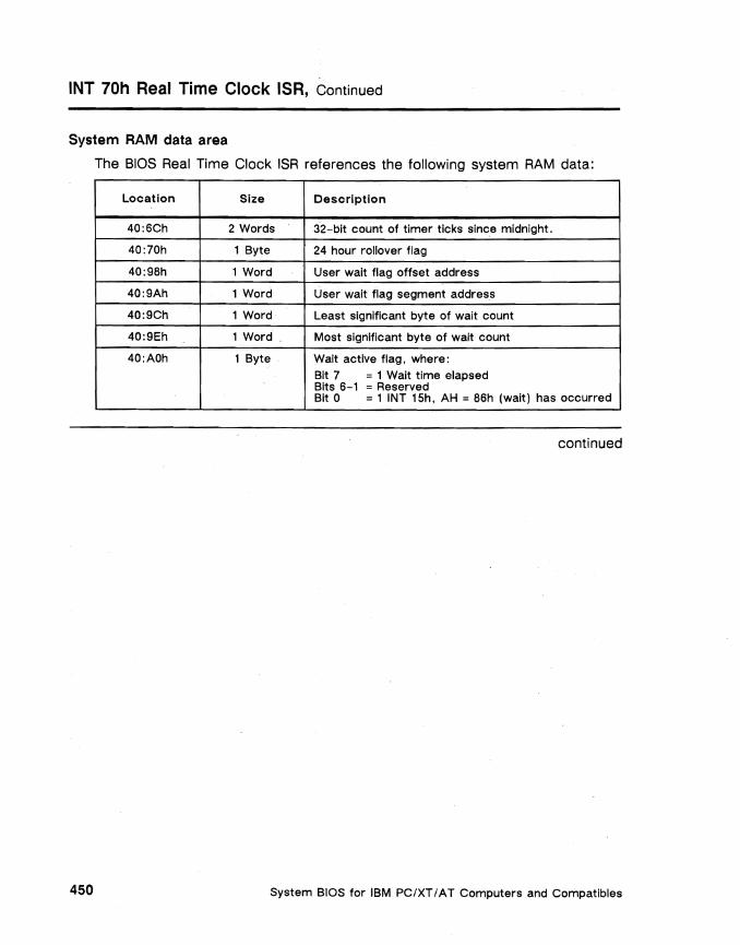
INT 70h Real Time Clock ISR, Continued
System RAM data area
The BIOS Real Time Clock ISR references the following system RAM data:
Location Size Description
40:6Ch 2 Words 32-bit count of timer ticks since midnight.
40:70h 1 Byte 24 hour rollover flag
40:98h 1 Word User wait flag offset address
40:9Ah 1 Word User wait flag segment address
40:9Ch 1 Word Least significant byte of wait count
40:9Eh 1 Word Most significant byte of wait count
40:AOh 1 Byte Walt active flag, where:
Bit 7 = 1 Wait time elapsed Bits 6-1 " Reserved Bit 0 " 1 INT 15h, AH = 86h (wait) has occurred
continued
System BIOS for iBM PC/XT/AT Computers and Compatibles 450

INT 70h Real Time Clock ISR, Continued
CMOS RAM data table areas
The BIOS Real Time Clock ISR references the following CMOS RAM data:
Location Size
OBh 1 Byte
OCh 1 Byte
ODh 1 Byte
Real Time Clock 1/0 Ports
Description
Status Register B, where:
Bit 7 =0 Run =1 Halt
Bit 6 =1 Enable periodic interrupt Bit 5 =1 Enable alarm interrupt Bit 4 =1 Enable update-ended interrupt Bit 3 =1 Enable square wave interrupt Bit 2 =1 Calendar is in binary format
=0 Calendar is in BCD format Bit 1 =1 24-hour mode
=0 12-hour mode Bit 0 =1 Enable Daylight Savings Time
Status Register C, where:
Bits 7-4 =IRQF, PF, AF, and UF flags, respectively
Bits 3-0 =Reserved
Status Register D, where:
Bit 7 =1 Real time clock has power Bits 6-0 =Reserved
The INT 70h Real Time Clock ISR references the following I/O ports:
Read/Write I/O Address Status Description
0020h R/W Master Programmable Interrupt Controller
0070h W CMOS RAM address register port, where:
Bit 7 =1 NMI disable = 0 NMI enabled
Bits 6-0 =0 CMOS RAM address
0071h R/W CMOS RAM data port
OOAOh R/W Slave Programmable Interrupt Controller
INT lAh Time-of-Day Service 451
INT 1 Ch Timer Tick ISR
Once INT OSh has serviced the clock, it issues a software INT 1 Ch. BIOS users may revector INT 1 Ch to their own routines.
Software INT 1 Ch points to a user routine to be executed on every system clock tick. The vector associated with this interrupt is invoked by the BIOS. Users should return control to the BIOS through an IRET. No action is taken by the BIOS when this interrupt is invoked unless this vector is modified by the caller. Any caller modifying the vector associated with this interrupt is responsible for saving and restoring all registers.
If not revectored, INT 1 Ch returns immediately to the caller with all registers preserved.
INT 4Ah Alarm ISR
When the alarm function is activated, this interrupt will occur at the time specified when INT 1 Ah Function 06h was last invoked. When the alarm time occurs, an INT 4Ah is generated. The caller must vector INT 4Ah to an alarm processing routine before invoking INT 1 Ah AH = 06h Real Time Clock Alarm.
Only AT BlOSs support this interrupt. It is not supported by PC or XT BlOSs.
System BIOS for IBM PC/XT/ A T Computers and Compatibles 452

Chapter 16
Single Function BIOS Services
Overview
Introduction
Most of the BIOS device services contain a group of functions intended to service a given device. For example, in the BIOS Parallel Printer service, invoking INT 17h with AH = OOh causes the service to execute its print character function. On the other hand, invoking INT 17h with AH = 01 h causes the service to execute its Initialize Printer Port function.
The single function services
In addition to its multifunction device services, the BIOS also contains several single function device services. Since these services perform only one function, it is not necessary to specify a function number in the AH register.
continued
Single Function BIOS Services 453

Overview, Continued
In this chapter
Because each single function service can be described on one or two pages, they are grouped into this one chapter.
This chapter presents the following topics:
• INT 05h Print Screen Service
• INT 11 h Equipment List Service
• INT 12h Memory Size Service
• INT 19h Bootstrap Loader Service
How to determine level of support
Throughout this book, the commonly accepted level of support for each ROM BIOS function is identified by the legend [PC], [XT] , and/or [AT] on the same line as the function title.
Legend Description
[PC] Function Is supported by original IBM PC BIOS only.
[XT] Function is supported by all IBM PC/XT and compatible ROM BlOSs.
Note: This level of support is contained in the ROM BiOS implemented in the majority of IBM PC and PC/XT compat-Ible systems.
[AT] Function is supported by all IBM PC/AT and compatible ROM BlOSs.
System BIOS for IBM PC/XT I AT Computers and Compatibles 454

INT OSh Print Screen Service [XT] [AT]
Description
The Print Screen Service:
• prints the contents of the entire current video screen to printer number 0 (LPT1) ,
• moves the cursor across the screen as the lines on the screen are printed,
• repositions the cursor position to its original position, and
• returns all registers to their original values.
Since the Print Screen Service takes a considerable amount of time to execute, interrupts are enabled throughout the routine.
The original PC BIOS did not support INT 05h, however, many PC-compatible BlOSs do. Nearly all XT and AT BlOSs support INT 05h. As a rule, if the system has a keyboard with a PrintScreen key, the system BIOS will support INT 05h.
How the service is invoked
INT 05h invokes the BIOS Print Screen Service.
The INT 05h vector resides at the interrupt vector table address 00: 14h. The BIOS initializes the INT 05h Print Screen Service vector to FOOO:FF54h.
INT 05h is usually invoked by the keyboard interrupt handler (INT 09h) when the PrtSc key is pressed. However, BIOS users may invoke INT 05h independently. For more information on INT 09h, refer to Chapter 8.
continued
Single Function BIOS Services 455

INT OSh Print Screen Service, Continued [XT] [AT]
System RAM Data
The Print Screen Service uses two system RAM data definitions. Both definitions are located in the BIOS Data Area (absolute address 400h to 500h) and are defined in the table below.
Location Size Description
40:84h 1 Byte Number of rows on screen (24/2S)
40:100h 1 Byte Print Screen Status Byte, where:
OOh = Print Screen Service inactive, or Print Screen Service successful upon return
01 h = Print Screen in progress FFh = Error
Input/Output
Input: None
Output: None (registers are preserved)
Error conditions
The Print Screen Service recognizes three kinds of error conditions. The table below summarizes the Print Screen Service error handling procedures.
If ... Then the Print Screen Service...
· · · ·
the printer is busy sets location 40: 1 OOh =FFh repositions cursor to original position preserves all registers returns to the caller
· · the printer is out of paper • repositions cursor to original position
preserves all registers returns to the caller · sets location 40: 100h =FFh
recursive print screen requests preserves all registers
· ·are made · returns to the caller
does not change location 40: 1 OOh (It was set to 01 by previous INT OSh request)
System BIOS for IBM PC/XT/AT Computers and Compatibles 456

INT 11 h Equipment List Service [XT] [AT]
Description
The Equipment List Service returns the contents of system RAM location 40:10h in AX. This memory location contains the system equipment list as determined by the BIOS POST routine.
How the service is requested
INT 11 h requests the Equipment List Service of the BIOS.
The INT 11 h vector resides at the interrupt vector table address 0:44h. The BIOS initializes the INT 11 h Equipment List Service vector to address FOOO:F84Dh.
Input/Output
Input: None
Output: Equipment List AX Contents of system RAM location 40: 1 Oh, where:
Bits 15-14 = Number of printer adapters Bits 13-12 = Reserved Bits 11-9 = Number of RS-232-C asynchronous adapters Bit 8 Reserved Bits 7-4 Number of diskette drives, (if Bit 0 = 1),
where: OOb = 1 diskette drive 01 b = 2 diskette drives
Bit 5-4 = Initial video mode, where: OOb = VGA/EGA/PGA 01 b = 40x25 color 10b = 80x25 color 11 b = 80x25 black and white
Bit 3 = Reserved Bit 2 1 If pointing device installed Bit 1 If math coprocessor installed Bit 0 = If diskette available for boot
Single Function BIOS Services 457
INT 12h Memory Size Service [XT) [AT)
Description
The Memory Size Service returns the contents of system RAM location 40: 13h in AX. This location contains the amount of available base memory in kilobytes as it is determined by the BIOS POST routine. The value returned reflects the amount of conventional memory in the system and does not report extended memory.
How the service is invoked
INT 12h invokes the BIOS Memory Size Service.
The INT 12h vector resides at the interrupt vector table address O:48h. The BIOS initializes the INT 12h memory size service vector to address FOOO:F841 h.
Input/Output
Input: None
Output: Available Base Memory AX = Contents of location 40: 13h in binary form
System BIOS for IBM PC/XT I AT Computers and Compatibles 458

INT 19h Bootstrap Loader Service [XT] [AT]
Description
The Bootstrap Loader Service attempts to load the 512-byte boot sector code from either diskette (usually drive A: only) or fixed disk to address 0: 7COOh , transferring control to the code segment at that address. The boot code is usually used to initialize the operating system.
The boot code is located in the first sector of the diskette (track O. head 0, sector 1) or in the first sector of the fixed disk (cylinder O. head O. sector 1).
Input/Output
Input: None
Output: None (registers are preserved)
How the service is invoked
INT 19h invokes the BIOS Bootstrap Loader Service.
The INT 19h vector resides at the interrupt vector table address 0:64h. The BIOS initializes the INT 19h Bootstrap Loader Service vector to address FOOO:E6F2h.
INT 19h is usually invoked by the POST routine at the end of all POST processing. BIOS users are free to invoke INT 19h independently of POST. Users should be aware. however. that invoking INT 19h does not reset or reinitialize the system but simply causes the system to reboot. For more information on POST and INT 19h. refer to Chapter 6.
continued
Single Function BIOS Services 459
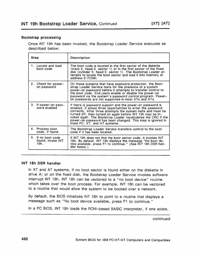
INT 19h Bootstrap Loader Service, Continued [XT] [AT]
Bootstrap processing
Once INT 19h has been invoked, the Bootstrap Loader Service executes as described below:
Step Description
1 . Locate and load The boot code is located in the first sector of the diskette boot code (track a, head a, sector 1) or hi the first sector of the fixed
disk (cylinder a, head a, sector 1). The Bootstrap Loader attempts to locate the boot sector and load it into memory at address a: 7caah.
2. Check for power- On those systems that have password protection, the Boot-on password strap Loader Service tests for the presence of a system
power-on password before it attempts to transfer control to the boot code. End users enable or disable the power-on password via the system's password control program. Power-on passwords are not supported in most XTs and A Ts.
3. If power-on pass- If there is password support and the power-on password is word enabled enabled, It allows three opportunities to enter the password
correctly. After three attempts the system halts and must be turned off, then turned on again before INT 19h may be invoked again. The Bootstrap Loader recalculates the CRC if the power-on password has been changed. This step is ignored in most PC, XT, and AT systems.
4. Process boot The Bootstrap Loader Service transfers control to the boot code, if found code if it has been located.
5. If no boot code If INT 19h does not find the boot sector code, it invokes INT found, invoke INT 18h. By default, INT 18h displays the message "No boot de18h. vice available, press F1 to continue." (See INT 18h DSR han
dier below.)
INT 18h DSR handler
In XT and AT systems, if no boot sector is found either on the diskette in drive A: or on the fixed disk, the Bootstrap Loader Service invokes software interrupt INT 18h. INT 18h can be vectored to a .. no boot device" routine which takes over the boot process. For example, INT 18h can be vectored to a routine that would allow the system to be booted over a network.
By default, the BIOS initializes INT 18h to point to a routine that displays a message such as .. No boot device available, press F1 to continue."
In a PC BIOS, INT 18h loads the ROM-based BASIC interpreter, if one exists.
continued
System BIOS for IBM PC/XT/AT Computers and Compatibles 460

INT 19h Bootstrap Loader Service, Continued eXT] [AT]
System RAM data
The Bootstrap Loader Service uses three system RAM data definitions. The definitions are located in the BIOS Data Area (absolute hex address 400h to SOOh) and are defined in the table below.
Location Size Description
12h 1 Byte Reserved for manufacturer's test, where:
Bits 7-1 = Reserved Bit 0 =1 Manufacturing test mode
=0 Non-manufacturing test mode
72h 1 Word System Reset Flag Where:
1234h = Bypass memory test 4321h =Preserve memory 0064h =Burn-in mode
75h 1 Byte Number of fixed disk drives
CMOS RAM data
The Bootstrap Loader Service references the following location in the CMOS RAM data area:
Location Size Description
OEh 1 Byte Diagnostic status, where:
Bit 7 = 1 RTC has lost power Bit 6 =1 CMOS RAM checksum is bad Bit 5 =1 Invalid configuration
information found at POST Bit 4 = 1 Memory size compare error found at
POST Bit 3 =1 Fixed disk or adapter fails initialization Bit 2 = 1 RTC time invalid Bit 1 =1 Adapters do not match configuration Bit 0 =1 Time-out in reading an adapter ID
continued
Single Function BIOS Services 461

INT 19h Bootstrap Loader Service, Continued [XT] [AT]
1/0 ports used
INT 19h, Bootstrap Loader Service, references the following I/O ports:
Read/Write I/O Address Status Description
0060h R/W Keyboard/auxiliary data port (AT only)
0064h W 8042 Commands (AT only)
0064h R 8042 Status (AT only), where: Bit 7 = 1 Parity error Bit 6 = 1 General time out Bit 5 = 1 Auxiliary output buffer full Bit 4 = 1 Inhibit switch Bit 3 = 1 Command
oData Bit 2 = System flag Bit 1 = 1 Input buffer full Bit 0 = 1 Output buffer full
0070h W CMOS RAM address register port (AT only), where: Bit 7 = 1 NMI disable
= 0 NMI enabled Bits 6-0 = 0 CMOS address
0071h R/W CMOS RAM data register port (AT only)
0063h R/W 8255 Command mode register (XT only), where: Bits 7-6 = Number of diskette drives, where:
OOb - 1 drive 01 b - 2 drives 10b - 3 drives 11 b - 4 drives
Bits 5-4 = Type of display at power-on, where: OOb - Reserved 01b - 40x25 color (mono mode) 10b - 80x25 color (mono mode) 11b - MDA (80x25)
Bits 3-2 = Memory on system board (256K chips), where: OOb - 256K 01b - 512K 10b - 576K 11b - 640K
Bits 3-2 = Memory on system board (64K chips), where: OOb - 64K 01b - 128K 10b - 192K 11b - 256K
Bits 1-0 = Reserved
System BIOS for IBM PC/XT/AT Computers and Compatibles 462

Appendix A
AT BIOS Error Codes and Messages
Introduction
This appendix lists, separately, the error messages generated by the IBM AT BIOS and the Phoenix AT-compatible BIOS.
In this appendix
The tables on the following pages present all Phoenix BIOS error messages, their causes and corrective actions. The following types of messages are documented:
• IBM BIOS POST and Boot Messages
• Phoenix BIOS POST and Boot Messages
• Phoenix BIOS Run-Time Messages
• Phoenix BIOS Beep Codes
• SETUP Messages
AT BIOS Error Codes and Messages 463

IBM BIOS POST and Boot Messages
IBM AT BIOS error messages
Error Number Message
101 System Board Error
102 System Board Error
103 System Board Error
104 System Board Error
105 System Board Error
106 System Board Error
107 System Board Error
108 System Board Error
109 System Board Error
161 System Options Not Set
162 System Options Not Set
163 Time and Date Not Set
164 Memory Size Error - (Run SETUP)
201 Memory Error
202 Memory Address Error
203 Memory Address Error
301 Keyboard Error
302 System Unit Keylock Is Locked
303 Keyboard or System Unit Error
304 Keyboard or System Unit Error
401 CRT Error
501 CRT Error
601 Diskette Error
602 Diskette Boot Record Error
1780 Disk 0 Failure
1781 Disk 1 Failure
1782 Disk Controller Failure
Possible Cause
System interrupt failed.
System timer failed.
System timer interrupt failed.
Protected mode operation failed.
Keyboard communication failure.
POST logic test problem.
NMI test failed.
Failed system timer test.
Problem with first 64K of RAM.
Possible bad battery.
Invalid checksum.
RTC failed.
CMOS RAM checksum error.
RAM failed test.
RAM failed test.
RAM failed test.
Keyboard not connected.
Keyboard is locked.
Keyboard chord or keyboard Itself Is bad.
Keyboard chord or keyboard itself is bad.
Monitor or video adapter bad.
Monitor or video adapter bad.
Diskette drive or controller bad.
No boot sector on diskette.
Primary fixed disk filed.
Secondary fixed disk failed.
Fixed disk controller failed.
continued
System BIOS for IBM PCIXTI AT Computers and Compatibles 464
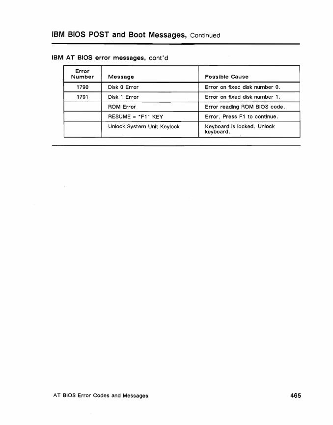
IBM BIOS POST and Boot Messages, Continued
IBM AT BIOS error messages, cont'd
Error Number Message
1790 Disk 0 Error
1791 Disk 1 Error
ROM Error
RESUME = "F1" KEY
Unlock System Unit Keylock
Possible Cause
Error on fixed disk number O.
Error on fixed disk number 1 .
Error reading ROM BIOS code.
Error. Press F1 to continue.
Keyboard is locked. Unlock keyboard.
AT BIOS Error Codes and Messages 465

Phoenix BIOS POST and Boot Messages
AT BIOS error messages
Message
Diskette configuration error
Diskette drive reset failed
Diskette drive 1 seek failure
Diskette drive 0 seek failure
Diskette drive reset failed
Diskette read failure strike F1 to retry boot
Display adapter failed; using alternate
Errors found; disk X: Failed Initialization
Errors found; incorrect configuration information memory size miscompare
Gate A20 failure
Hard disk configuration error
Hard disk controller failure
Hard disk failure
Hard disk read failure strike F1 to retry boot
FDD controller failure
FDD A Is not Installed
Possible Cause
The specified configuration is not supported.
The diskette adapter has failed.
The B: drive failed or Is missing.
The A: drive has either failed or is missing.
The diskette adapter has failed.
The diskette is either not formatted or defective. . The color/monochrome
switch Is set wrong. . The primary video adapter failed.
POST reports hard disk configuration Information Is Incorrect.
POST reports the size of base or expansion memory does not agree with configuration information.
Protected mode cannot be enabled.
The specified configuration Is not supported.
The controller card has failed.
Bad disk.
Defective fixed disk.
Disk and diskette controller failed.
Can not find diskette controller for diskette drive A
Solution
Change the configuration.
Check the diskette adapter.
Check the B: drive.
Check the A: drive.
Check the diskette adapter.
Replace the diskette with a bootable diskette and retry.
. Change the switch to the correct setting. . Check the primary video adapter.
Rerun SETUP and enter correct hard disk information.
Rerun SETUP and enter correct memory size.
Check the system board.
Correct the fixed disk configuration.
Replace the controller card.
Retry boot. If that doesn't work, replace the hard disk.
Retry boot. if that doesn't work, replace the hard disk.
Replace the controller card.
Either Install or replace the controller card.
continued
System BIOS for IBM PC/XT / AT Computers and Compatibles 466

Phoenix BIOS POST and Boot Messages, Continued
AT BIOS error messages, cont'd
Message
FDD B Is not Installed
Invalid configuration Informatlon - please run SETUP program
Keyboard clock line failure
Keyboard data line failure
Keyboard controller failure
Keyboard stuck key failure
Memory address line fallure at hex-value, read hex-value, expecting hex-value
Memory data line failure at hex-value. read hex-value, expecting hex-value
Memory high address line failure at hex-value, read hex-value. expecting hex-value
Memory double word logic failure at hex-value, read hex-value, expect-Ing hex-valu.e
Memory odd/even logic failure at hex-value, read hex-value, expecting hex-value
Memory parity failure at hex-value, read hex-value, expecting hex-value
Possible Cause
Can not find diskette controller for diskette drive B
· Memory size Is Incorrect.
· Display adapter [s configured Incorrectly.
· Wrong number of diskette drives.
Either the keyboard or the keyboard cable connection Is defective.
The keyboard controller firmware has failed.
A key(s) is jammed.
Circuitry associated with the memory chips has failed.
One of the memory chips or associated circuitry has failed.
Circuitry associated with the memory chips has failed.
Memory chip circuitry failed.
Circuitry associated with the memory chips has failed.
One of the parity memory chips has failed.
Solution
Either Install or replace the controller card.
Run the SETUP utility.
Make sure the keyboard cable and keyboard are connected properly. -Check the keyboard controller.
Try pressing the key (s) again.
Check the circuitry.
Replace the memory chips.
Check the circuitry.
Replace the memory chip.
Check the circuitry.
Try replacing the memory chips.
continued
AT BIOS Error Codes and Messages 467
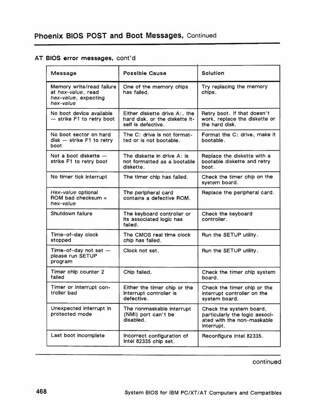
Phoenix BIOS POST and Boot Messages, Continued
AT BIOS error messages, cont'd
Message
Memory write/read failure at hex-value, read hex-value, expecting hex-value
No boot device available - strike F1 to retry boot
No boot sector on hard disk - strike F1 to retry boot
Not a boot diskette strike F1 to retry boot
No timer tick Interrupt
Hex-value optional ROM bad checksum = hex-value
Shutdown failure
Time-of-day clock stopped
Time-of-day not set please run SETUP program
Timer chip counter 2 failed
Timer or Interrupt controlier bad
Unexpected interrupt in protected mode
Last boot Incomplete
Possible Cause
One of the memory chips has failed.
Either diskette drive A:, the hard disk, or the diskette itself Is defective.
The C: drive Is not formatted or is not bootable .
The diskette in drive A: is not formatted as a bootable diskette.
The timer chip has failed.
The peripheral card contains a defective ROM.
The keyboard controlier or its associated logic has failed.
The CMOS real time clock chip has failed.
Clock not set.
Chip failed.
Either the timer chip or the interrupt controlier is defective.
The nonmaskable interrupt (NMI) port can't be disabled.
Incorrect configuration of Intel 82335 chip set.
Solution
Try replacing the memory chips.
Retry boot. If that doesn't work, replace the diskette or the hard disk.
Format the C: drive, make it bootable.
Replace the diskette with a bootable diskette and retry boot.
Check the timer chip on the system board.
Replace the peripheral card.
Check the keyboard controlier.
Run the SETUP utility.
Run the SETUP utility.
Check the timer chip system board.
Check the timer chip or the interrupt controller on the system board.
Check the system board, particularly the logic associated with the non-maskable interrupt.
Reconfigure Intel 82335.
continued
System BIOS for IBM PC/XT/ AT Computers and Compatibles 468

Phoenix BIOS POST and Boot Messages, Continued
Informational messages
Message
nnnK Base Memory
nnnK Expanded Memory
nnnK Extended Memory
nnnK Extra Memory
nnnK Standard Memory
Decreasing available memory
Memory tests terminated by keystroke
Strike the F1 key to continue
Base Memory size =64K
Extended Memory size =OOOOOK
Meaning
The amount of base memory that tested successfully.
The amount of expanded memory that tested successfully.
The amount of extended memory that tested successfully.
The amount of extra memory that tested successfully.
The amount of standard memory that tested successfully.
This message immediately follows any memory error message. and informs you that the memory chips are failing.
This message indicates that you have pressed the Spacebar while the memory tests were running. This stops the memory tests.
This message Indicates that an error was found during POST. Pressing the F1 key allows the system to attempt to boot.
Used in reporting base memory for Extended Features.
Used In reporting extended memory size for Extended Features.
AT BIOS Error Codes and Messages 469

Phoenix BIOS Run-Time Messages
Run-time messages
Run-time messages are displayed if an error occurs after the boot procedure is complete.
Message Possible Cause Solution
110 card parity interrupt The peripheral card has Type (S)hut off NMI. at address. Type (S)hut off NMI, (R)eboot, other keys to continue
failed. Note: This will only temporarily allow the user to continue. The user must replace the peripheral card.
Memory parity interrupt at address. Type (S)hut off NMI, (R)eboot, other keys to continue
A memory chip(s) has fa.iled.
Type (S)hut off NMI.
Note: This will,only temporarily allow the user to continue. The user must replace the memory chip(s).
Unexpected HW Interrupt This could be any Check the hardware. Interrupt at address. hardware-related problem. Type (R)eboot, other keys to continue Note: Not displayed if the
extended interrupt handler is not enabled.
Unexpected SW interrupt Interrupt at address. Type (R)eboot, other keys to continue
There is an error ( s) in the software program.
Note: Not displayed If the extended interrupt
Try turning the machine off and then on again. If that doesn't work, check the program.
handler is not enabled.
Unexpected type 02 Interrupt at address. Type (S)hut off NMI, (R)eboot, other keys to continue
There is an error(s) in the software program.
Note: Not displayed if the extended interrupt
Try turning the machine off and then on again. If that doesn't work, check the program.
handler is not enabled.
System BIOS for IBM PC/XT / AT Computers and Compatibles 470
Phoenix BIOS Beep Codes
Description
Sometimes POST errors cannot be reported on the screen. When an error occurs before the screen is initialized or when the system is set to loop on the system board tests, then the screen cannot display the error message. Systems with a Phoenix AT-compatible BIOS will then generate beep codes, which may be used to identify a POST error that occurs when the screen is not available.
Example
A 2-1-4 beep code (a burst of 2 beeps, a single beep, and a burst of 4 beeps) indicates a failure of bit 3 in the first 64K of RAM.
continued
A T BIOS Error Codes and Messages 471
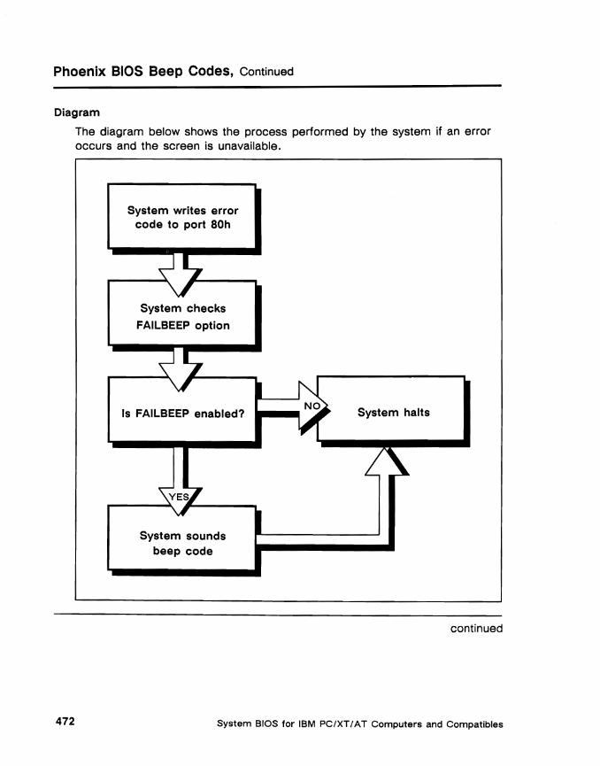
Phoenix BIOS Beep Codes, Continued
Diagram
The diagram below shows the process performed by the system if an error occurs and the screen is unavailable.
System writes error code to port SOh
System checks
FAILBEEP option
Is FAILBEEP enabled? System halts
System sounds beep code
continued
System BIOS for IBM PC/XTI AT Computers and Compatibles 472

Phoenix BIOS Beep Codes, Continued
Using Beep Codes
The table below shows the errors for which beep codes and screen messages are used:
System Board Failure Off board
Fatal Non-fatal Failure
Looping on sys- Beep and halt Beep and halt Not applicable tem board tests (MAN LOOP set to True)
Normal power Beep and halt Screen message and Screen message and on (MANLOOP prompt to 'Press F1 prompt to 'Press F1 set to False) to continue' to continue'
List of Beep Codes
The Beep Codes for fatal and non-fatal system board errors are listed separately on the following pages.
Note: No beep code is sounded if a test is aborted while in progress. The contents of port 80h can be read to identify the area of failure.
continued
AT BIOS Error Codes and Messages 473
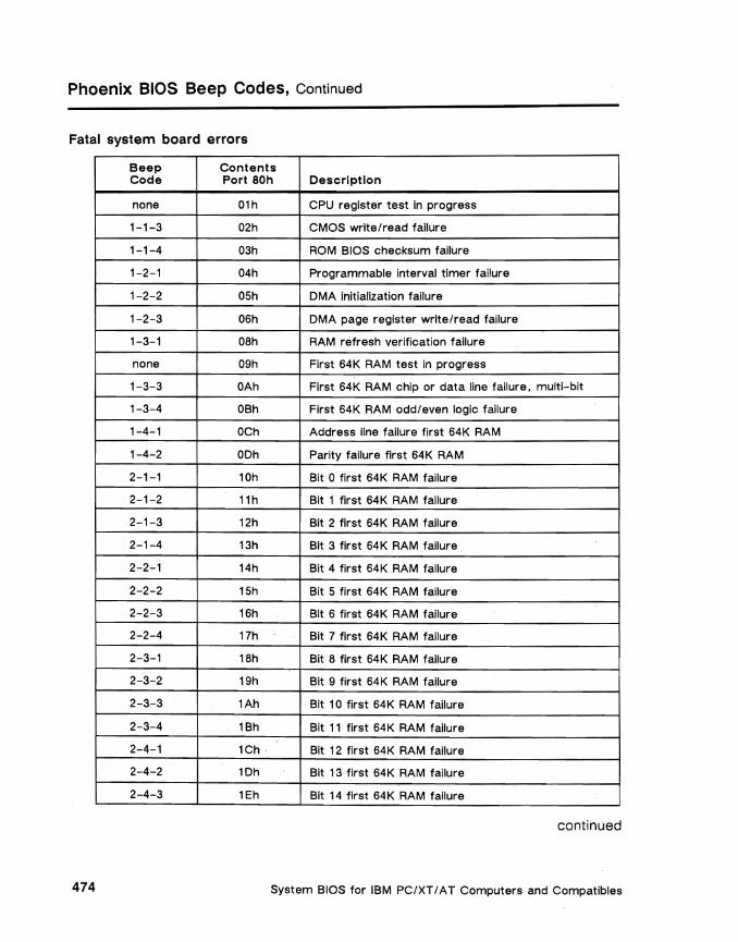
Phoenix BIOS Beep Codes, Continued
Fatal system board errors
Beep Contents Code Port BOh
none 01h
1-1-3 02h
1-1-4 03h
1-2-1 04h
1-2-2 05h
1-2-3 06h
1-3-1 08h
none 09h
1-3-3 OAh
1-3-4 OBh
1-4-1 OCh
1-4-2 ODh
2-1-1 10h
2-1-2 11 h
2-1-3 12h
2-1-4 13h
2-2-1 14h
2-2-2 15h
2-2-3 16h
2-2-4 17h
2-3-1 18h
2-3-2 19h
2-3-3 1Ah
2-3-4 1Bh
2-4-1 1Ch
2-4-2 1Dh
2-4-3 1Eh
Description
CPU register test in progress
CMOS write/read failure
ROM BIOS checksum failure
Programmable interval timer failure
DMA initialization failure
DMA page register write/read failure
RAM refresh verification failure
First 64K RAM test in progress
First 64K RAM chip or data line failure, multi-bit
First 64K RAM odd/even logic failure
Address line failure first 64K RAM
Parity failure first 64K RAM
Bit 0 first 64K RAM failure
Bit 1 first 64K RAM failure
Bit 2 first 64K RAM failure
Bit 3 first 64K RAM failure
Bit 4 first 64K RAM failure
Bit 5 first 64K RAM failure
Bit 6 first 64K RAM failure
Bit 7 first 64K RAM failure
Bit 8 first 64K RAM failure
Bit 9 first 64K RAM failure
Bit 10 first 64K RAM failure
Bit 11 first 64K RAM failure
Bit 12 first 64K RAM failure
Bit 13 first 64K RAM failure
Bit 14 first 64K RAM failure
continued
System BIOS for IBM PC/XT / A T Computers and Compatibles 474
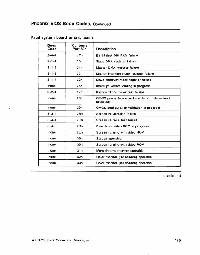
Phoenix BIOS Beep Codes, Continued
Fatal system board errors, cont' d
Beep Contents Code Port SOh Description
2-4-4 1Fh Bit 15 first 64K RAM failure
3-1-1 20h Slave DMA register failure
3-1-2 21h Master DMA register failure
3-1-3 22h Master interrupt mask register failure
3-1-4 23h Slave interrupt mask register failure
none 25h Interrupt vector loading in progress
3-2-4 27h Keyboard controller test failure
none 28h CMOS power failure and checksum calculation in progress
none 29h CMOS configuration validation in progress
3-3-4 2Bh Screen initialization failure
3-4-1 2Ch Screen retrace test failure
3-4-2 2Dh Search for video ROM in progress
none 2Eh Screen running with video ROM
none 30h Screen operable
none 30h Screen running with video ROM
none 31h Monochrome monitor operable
none 32h Color monitor (40 column) operable
none 33h Color monitor (80 column) operable
continued
AT BIOS Error Codes and Messages 475
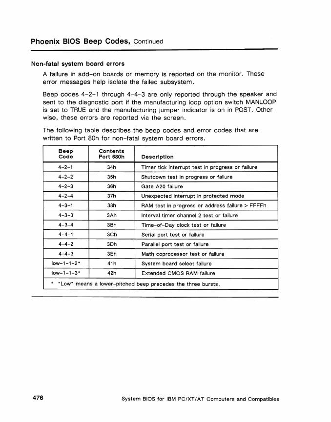
Phoenix BIOS Beep Codes, Continued
Non-fatal system board errors
A failure in add-on boards or memory is reported on the monitor. These error messages help isolate the failed subsystem.
Beep code~ 4-2-1 through 4-4-3 are only reported through the speaker and sent to the diagnostic port if the manufacturing loop option switch MAN LOOP is set to TRUE and the manufacturing jumper indicator is on in POST. Otherwise, these errors are reported via the screen.
The following table describes the beep codes and error codes that are written to Port BOh for non-fatal system board errors.
Beep Contents Code Port 680h Description
4-2-1 34h Timer tick interrupt test in progress or failure
4-2-2 35h Shutdown test In progress or failure
4-2-3 36h Gate A20 failure
4-2-4 37h Unexpected interrupt in protected mode
4-3-1 38h RAM test in prQ!;Iress or address failure> FFFFh
4-3-3 3Ah Interval timer channel 2 test or failure
4-3-4 3Bh Time-of-Day clock test or failure
4-4-1 3Ch Serial port test or failure
4-4-2 3Dh Parallel port test or failure
4-4-3 3Eh Math coprocessor test or failure
low-1-1-2* 41h System board select failure
low-1-1-3* 42h Extended Cfy10S RAM failure
• "Low· means a lower-pitched beep precedes the three bursts.
System BIOS for IBM PC/XT/ AT Computers and Compatibles 476
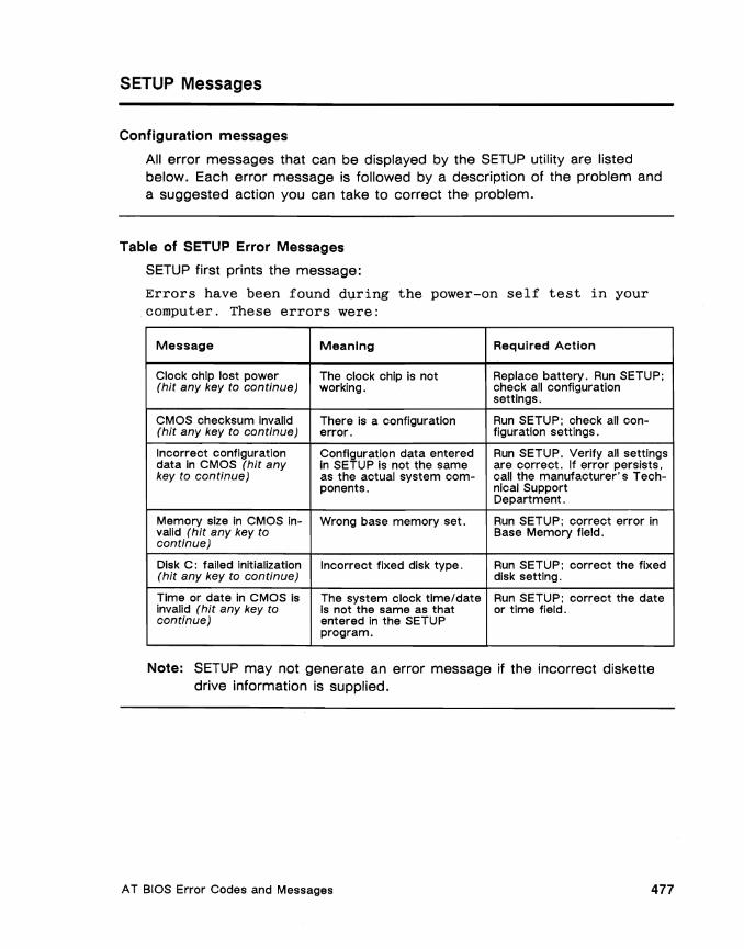
SETUP Messages
Configuration messages
All error messages that can be displayed by the SETUP utility are listed below. Each error message is followed by a description of the problem and a suggested action you can take to correct the problem.
Table of SETUP Error Messages
SETUP first prints the message:
Errors have been found during the power-on self test in your computer. These errors were:
Message
Clock chip lost power (hit any key to continue)
CMOS checksum invalid (hit any key to continue)
Incorrect configuration data in CMOS (hit any key to continue)
Memory size in CMOS invalid (hit any key to continue)
Disk C: failed initialization (hit any key to continue)
Time or date in CMOS is Invalid (hit any key to continue)
Meaning
The clock chip is not working.
There is a configuration error.
Configuration data entered in SETUP is not the same as the actual system components.
Wrong base memory set.
Incorrect fixed disk type.
The system clock time/date Is not the same as that entered in the SETUP program.
Required Action
Replace battery. Run SETUP; check all configuration settings.
Run SETUP; check all configuration settings.
Run SETUP. Verify all settings are correct. If error persists. call the manufacturer's Technical Support Department.
Run SETUP; correct error in Base Memory field.
Run SETUP; correct the fixed disk setting.
Run SETUP; correct the date or time field.
Note: SETUP may not generate an error message if the incorrect diskette drive information is supplied.
AT BIOS Error Codes and Messages 477

Appendix B
XT BIOS Error Messages
Introduction
This appendix describes the power-on self test and boot messages that may be generated by both the IBM and the Phoenix XT BIOS.
These messages may be divided into the following types:
• Beep Code • IBM XT BIOS POST Messages
• Phoenix XT BIOS POST and Boot Messages
• Phoenix XT BIOS Run-Time Messages
Each of these types of messages are discussed below.
XT BIOS Error Messages 479
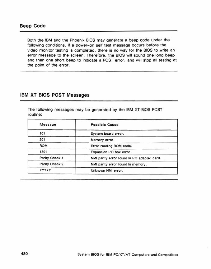
Beep Code
Both the IBM and the Phoenix BIOS may generate a beep code under the following conditions. If a power-on self test message occurs before the video monitor testing is completed, there is no way for the BIOS to write an error message to the screen. Therefore, the BIOS will sound one long beep and then one short beep to indicate a POST error, and will stop all testing at the point of the error.
IBM XT BIOS POST Messages
The following messages may be generated by the IBM XT BIOS POST routine:
Message Possible Cause
101 System board error.
201 Memory error.
ROM Error reading ROM code.
1801 Expansion 1/0 box error.
Parity Check 1 NMI parity error found In 1/0 adapter card.
Parity Check 2 NMI parity error found In memory.
11111 Unknown NMI error.
System BIOS for IBM PC/XT IAT Computers and Compatibles 480
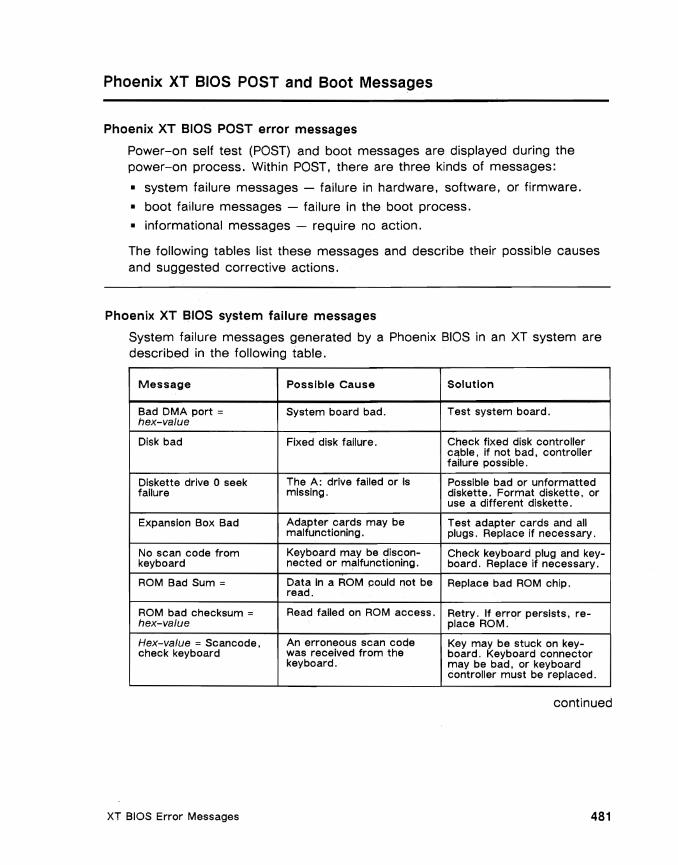
Phoenix XT BIOS POST and Boot Messages
Phoenix XT BIOS POST error messages
Power-on self test (POST) and boot messages are displayed during the power-on process. Within POST, there are three kinds of messages:
• system failure messages - failure in hardware, software, or firmware.
• boot failure messages - failure in the boot process.
• informational messages - require no action.
The following tables list these messages and describe their possible causes and suggested corrective actions.
Phoenix XT BIOS system failure messages
System failure messages generated by a Phoenix BIOS in an XT system are described in the following table.
Message
Bad DMA port = hex-value
Disk bad
Diskette drive 0 seek failure
Expansion Box Bad
No scan code from keyboard
ROM Bad Sum =
ROM bad checksum = hex-value
Hex-value = Scancode, check keyboard
Possible Cause
System board bad.
Fixed disk failure.
The A: drive failed or Is missing.
Adapter cards may be malfunctioning.
Keyboard may be disc onnected or malfunctioning.
Data In a ROM could not be read.
Read failed on ROM access.
An erroneous scan code was received from the keyboard.
Solution
Test system board.
Check fixed disk controller cable, if not bad, controller failure possible.
Possible bad or unformatted diskette. Format diskette, or use a different diskette.
Test adapter cards and all plugs. Replace if necessary.
Check keyboard plug and keyboard. Replace if necessary.
Replace bad ROM chip.
Retry. If error persists, replace ROM.
Key may be stuck on keyboard. Keyboard connector may be bad, or keyboard controller must be replaced.
continued
XT BIOS Error Messages 481

Phoenix XT BIOS POST and Boot Messages, Continued
Phoenix XT BIOS system failure messages, cont'd
Message Possible Cause Solution
Stuck key scancode = hex-value
Key stuck on keyboard. Loosen stuck key. Check scan code table to identify key.
Timer or Interrupt Controller Bad
Interrupt controller or timer chip inoperative.
Replace system board.
Timer chip counter 2 failed
Timer bad. Replace'system board or timer chip.
Phoenix XT BIOS boot failure messages
Boot failure messages generated by a Phoenix BIOS in an XT system are described in the following table.
Message Possible Cause Solution
128K not OK. parity First 128K of RAM failed Reboot. If message repeats. disabled parity test. replace bad RAM chip($).
Keyboard bad Keyboard failed POST Retry. If message persists. tests. replace keyboard.
Error. Press F1 key to A recoverable error Press F1 to continue (there continue. occurred. may be errors). or reboot.
Non-System disk or disk No boot diskette or disk Use a system disk to boot error. Press a key to available. the system.continue.
Disk boot error. Replace Boot data not readable Use a boot diskette/disk to and strike key or retry. from boot device. boot system.
RAM bad Memory failed POST tests. Replace bad RAM chips.
continued
System BiOS for IBM PC/XT/AT Computers and Compatibles 482

Phoenix XT BIOS POST and Boot Messages, Continued
Phoenix XT BIOS informational messages
Informational messages generated by a Phoenix BIOS in an XT system are described in the following table.
Message Possible Cause Solution
RAM test Information only. No action required.
Oh optionai Information only. No action required.
Hard disk wait complete information only. No action required.
Memory space preserved Information only. No action required.
XT BIOS Error Messages 483

Phoenix XT BIOS Run-Time Messages
Run-time message table
Run-time messages generated by a Phoenix BIOS are displayed if an error occurs after the boot procedure is complete.
Message
8087 NMI at address. Type (Slhut off NMI. (Rleboot, other keys to continue.
Memory parity NMI at address. Type (Slhut off NMI, (Rleboot, other keys to continue.
Unexpected HW interrupt interrupt at address. Type (Rleboot, other keys to continue.
Unexpected SW Interrupt interrupt at address. Type (Rleboot, other keys to continue.
1/0 card NMI at address. Type (Slhut off NMI, (Rleboot, other keys to continue.
Possible Cause
An NMI occurred on access to the math coprocessor.
A memory chlp(sl has failed.
This could be any hardware-related problem. Note: Not displayed if the
extended interrupt handler is not enabled.
There Is an error(sl in the software program. Note: Not displayed if the
extended interrupt handler Is not enabled.
An NMI occurred on access to an adapter card.
Solution
Type (Slhut off NMI.
Note: This will only temporarify allow you to continue. You must replace the peripheral card.
Type (Slhut off NMI. Note: This will only tempo
rarily allow you to continue. You must replace the memory chip(sl.
Check the hardware devices for loose cables, malfunctions, and other problems.
Turn the machine off and then on again. If that doesn't work, check the program.
Turn the machine off and then on again. If that doesn't work, replace the adapter card.
System BIOS for IBM PC/XT/AT Computers and Compatibles 484
Glossary
Adapter Card
A circuit board that can be installed into one of the expansion slots inside a PC, XT, AT, or IBM-compatible computer in order to expand the capabilities of the computer.
Adapter ROM
The read-only memory on the adapter, which contains code to control the adapter device. An adapter is a peripheral card that extends the operation of the system. For example, a fixed disk drive controller is an adapter that may have an adapter ROM.
Address Bus
One or more lines (conductors) that carry address codes from the microprocessor to all parts of the system.
American National Standard Code for Information Exchange (ASCII)
A standard code, consisting of character, control, and graphic codes of 7 bits each (8 bits counting the parity bit).
Analog
Data transmitted in a continuously varying physical quality.
Arbitration
Arbitration is a process through which devices compete for possession of the channel on a prioritized basis.
continued
Glossary 485
Glossary, Continued
Arbitration Level Arbitration levels are the levels of priority assigned to devices that compete for possession of the channel.
AT-Compatible Computer
Any computer that can run software programs written for an IBM AT computer.
Basic Input/Output System (BIOS)
Systems software that interfaces between the operating system and hardware.
BIOS Service A software routine that services a given peripheral device, and provides an interface between the operating system and the hardware. These services are single task, call/return functions.
Bits per second (BPS)
A unit of measure that represents the number of discrete bits transmitted by a device in one second.
Block Check Character (BCC)
An element in the checksum calculations in cyclic redundancy checking.
Boot
Process of starting the computer.
Buffer
An area of storage temporarily reserved for I/O operations.
Burst Mode
Burst mode is a method of DMA transfer that allows a device to remain inactive for long periods and then send large amounts of data in a short time.
Bus
One or more lines (conductors) that carry signals or power.
Bus High Enable (BHE)
A line on the 80286 processor that produces a signal, used in conjunction with the address 0 signal, to specify if data is transferred in words or bytes.
continued
System BIOS for IBM PC/XT/AT Computers and Compatibles 486

Glossary, Continued
Byte
Eight contiguous bits; a bit is the smallest item of information that a computer can process.
Cache
Method of using a fast device to speed up access to a slow device.
Central Processing Unit (CPU)
The main processing component of the microprocessor.
Channel
A path constructed specifically for moving data.
Command Control Block (CCB)
Disk 1/0 data structure.
Command Specify Block (CSB)
Disk I/O data structure.
Complementary Metal Oxide Semiconductor (CMOS)
In PC, XT. or AT compatibles, it is low-power memory that is batterybacked and is therefore not lost when the computer is turned off.
Configuration
The process of setting up all the parts of the computer so they run effectively.
Conventional memory
Memory located between addresses 0 and 1 MB. The memory that can be addressed by DOS.
Cyclic Redundancy Check (CRC)
A method of redundancy check where the check key is produced by a cyclic or repeating algorithm. A common means of error checking.
Cylinder
Tracks on a diskette or fixed disk that can be accessed without moving the read/write heads.
Default
A value, setting. or option that is assigned by the program or system.
continued
Glossary 487

Glossary, Continued
Digital-to-Analog Converter (DAC)
Used in VGA hardware to convert command and data when interfacing between digital computer hardware and an analog monitor.
Direct Memory Access (DMA)
Direct Memory Access is a means for I/O devices to transfer data directly to and from system memory without the intervention of the microprocessor. This significantly decreases I/O processing by the microprocessor.
Disk Operating System (DOS)
Short for PC-DOS and MS-DOS. DOS, like other operating systems, organizes the files and memory for other programs.
DMA Controller
A DMA controller is a device which gives addresses and control signals to the device that has won the bus through arbitration. The controller does not enter into the arbitration itself.
DMA Device
A DMA device enters into arbitration for the channel. If it wins, it receives addresses and control signals from the DMA controller so it can read or write data.
Dual Inline Package (DIP)
A method of organizing computer switches.
Erasable Programmable Read-Only Memory (EPROM)
A ROM device that can be erased and reprogrammed at anytime by a special machine.
Error Checking and Correction (ECC)
The process of detecting and correcting all single-bit errors using an algorithm that tests the accuracy of the transmitted data.
Expanded Memory
For AT-compatible systems, up to 32 MB of additional "paged" memory above the DOS 640K limit. Application programs written according to LIM EMS or AST EEMS specifications can use this type of memory. Examples of such programs are Lotus 1-2-3, Symphony and Framework.
continued
System BIOS for IBM PCfXT f AT Computers and Compatibles 488
Glossary, Continued
Expanded Memory Specification (EMS)
For AT-compatible systems, a specification and protocol established by a consortium of computer manufacturers, principally Lotus, Intel, and Microsoft (LIM), which establishes a set of rules for organizing and accessing expanded memory.
Extended Expanded Memory Specification (EEMS)
A specification and protocol established by a consortium of computer manufactures, principally AST, Quadram, and Ashton-Tate, which establishes a set of rules for organizing and accessing expanded memory.
Extended Memory
The memory above 1 MB. XENIX and IBM's VDISK can use this memory, but DOS and almost all application programs cannot, since use of the protected mode of the Intel 80286, 80386SX, or 80386 microprocessor is required.
Fixed Disk (Hard Disk)
A magnetic storage device consisting of a drive mechanism with permanently installed metallic disks; a "filing cabinet" for the computer.
Hardware
The physical equipment and components in the computer system.
Head
The read/write head on a diskette or fixed disk drive. The device that provides access to the data on the media.
Interrupt
The suspending of microprocessor program execution by a demand for attention coming from a peripheral device. After the interrupt has been serviced, the suspended microprocessor task can be resumed where it was broken off by the interrupt.
Kilobytes (K)
1024 bytes.
Known State
When a device is initialized or reset, and then set to a particular preestablished condition, it is said to be in a known state.
continued
Glossary 489
Glossary, Continued
Low Level Format Electronic equivalent of drawing a detailed street map on the fixed disk. The electronic markings tell the system at what points to start and end reads and writes.
Main Memory
The memory between 0 and 1 MS. Another term for conventional memory.
Megabyte (MB)
One million, or 1024 x 1024 bytes.
Memory
A device that can store data recorded in it and from which the data can be retrieved.
Microprocessor
Central processing unit, or "brain" of the computer.
Modified Frequency Modulation Traditional method of formatting data on a fixed disk. This technique involves a varying the amplitude and frequency of a signal to a fixed disk.
Multitasking
Multitasking programs execute multiple program modules simultaneously. Information input into one module does not need to be processed completely before information can be .input into another module.
Offset
A method of addressing that defines an address as relative to the beginning of a memory segment.
Operating System
Generic systems software which controls the execution of applications software.
Parameter
Value, option, or setting that can be set in two or more ways.
Power-On Self Test (POST)
A program that tests all parts of the computer every time you turn on the computer.
continued
System BIOS for IBM PC/XT/AT Computers and Compatibles 490

Glossary, Continued
Program
A set of instructions defining the operations of a computer in order to achieve the desired results.
Protected Address Mode (Protected Mode)
One of two 80286 or three 80386 memory addressing modes. In protected virtual address mode, the 80386/80286 uses all address lines. This allows addressing of up to 16 megabytes of physical memory in an 80286 and 4 GB in an 80386. The 80286 processor's internal memory management allows addressing of an additional 1 GB of virtual memory in protected mode (the 80386 up to 64 Terabytes). Protected mode addresses are specified in selector:offset format.
Real Address Mode
One of two 80286 memory addressing modes (the 80386 has three). In real address mode, the 80286 and 80386 microprocessors use 20 address lines, thus allowing memory addressing of up to 1 megabyte of physical memory (220). Real address mode· does not support virtual memory addressing. Real mode addresses are specified in segment:offset format.
Segment
A unit of contiguous, one-dimensional address space. In real mode, these address blocks are 64K in size, referenced by one byte. In protected mode, programs can allocate segments of any size they require up to 64K.
Selector
A value contained in a segment register (such as the CS, OS, SS, or ES segment registers) when in protected mode. This value determines what segment is currently being used; e.g., with CS, what segment is being used for executing code.
Single-Tasking
Single-tasking operating systems can only execute one program module or routine at a time. Information input into a module or routine mustbe processed completely before information can be input into another module.
Software
A comprehensive term used to identify all of the non hardware components of a computer. Software includes computer programs and data.
continued
Glossary 491

Glossary, Continued
System Board
A large circuit board that holds most of the main electronic parts of the computer.
System Board ROM
Read-only memory chips that reside on the system board and provide control information for various system components.
Task
In an 80386, a task is the execution of a single process or set of instructions to perform a particular function. It is not the same as an operating system task.
Time-Out
When the interval of time expected for a certain process (an interrupt) to occur is exceeded.
Track
A segment of a diskette or fixed disk that is parallel to the edge of the media and that can be accessed by the drive read/write head without the head moving.
Virtual 8086 Mode (80386 only)
A way of emulating the 8086 or 8088 microprocessors on the 80386. The 8086 program runs in protected mode as a task that can run with multiple 8086 virtual tasks, as well as alongside other multiprogrammed 80386 tasks.
Write Precompensation
A procedure where the timing of the head current on a diskette or fixed disk drive is varied depending on the head's position (anywhere from outer tracks to the inner tracks) in order to keep the Write signal constant. Often given as a cylinder number, as in the cylinder number where the write proecompensation procedure is to begin.
System BIOS for IBM PC/XT/AT Computers and Compatibles 492

Additional Resources
The following books provide additional material related to the PC, XT, and AT BlOSs:
Dettman, Terry R. DOS Programmer's Reference. Carmel, IN: Que® Corporation, 1988.
Duncan, Ray. Advanced MS-DOS Programming. Redmond, WA: Microsoft Press, 1986.
Duncan, Ray. IBM® ROM BIOS. Redmond, WA: Microsoft Press, 1988.
Intel Corporation. Introduction to the 80286. Santa Clara, CA: Intel Corporation, 1982.
Intel Corporation. 80286 Programmer's Reference Manual. Santa Clara, CA: Intel Corporation, 1983.
Intel Corporation. 80287 Programmer's Reference Manual. Santa Clara, CA: Intel Corporation, 1984.
Intel Corporation. Introduction to the 80386. Santa Clara, CA: Intel Corporation, 1985.
Intel Corporation. 80386 Programmer's Reference Manual. Santa Clara, CA: Intel Corporation, 1986.
Intel Corporation. 80387 Programmer's Reference Manual. Santa Clara, CA: Intel Corporation, 1987.
continued
Additional Resources 493
Additional Resources, Continued
International Business Machines Corporation. IBM Personal Computer AT Technical Reference. Boca Raton, FL: International Business Machines Corporation, 1984.
International Business Machines Corporation. IBM Personal Computer XT and Portable Personal Computer Technical Reference. Boca Raton, FL: International Business Machines Corporation, 1986.
Kliewer, Bradley Oyck. EGAIVGA Programmer's Reference Guide. New York, NY: McGraw-Hili Book Company, 1988
Norton, Peter. Inside the IBM® PC. New York, NY: Brady Books, a division of Simon and Schuster, 1986.
Norton, Peter and Wilton, Richard. The New Peter Norton Programmer's Guide to the IBM® PC and PSI2®. Redmond, WA: Microsoft Press, 1988.
Wadlow, Thomas A. Memory Resident Programming on the IBM PC. Reading, MA: Addison-Wesley Publishing Co., Inc., 1987.
Wilton, Richard. Programmer's Guide to PC® and PSI2'M Video Systems. Redmond, WA: Microsoft Press, 1987.
System BIOS for IBM PC/XT I AT Computers and Compatibles 494
tndex
A Abbreviations, xxvii-xxx
ACK signal, 418
Acronyms, xxvii-xxx
Active character blocks, 253
Active display code, 250
Active display pages 1/0 port for, 250 writing to, 218-219
Adapters asynchronous communications, 31,
39, 41, 45, 47, 274, 421 fixed disk, 84-85 printer, 31, 47, 121 video, 2, 162
error messages for, 466 hardware components of,
171-172 mode support by, 170 types of, 1 68 video ROM for, switching of, with
system video, 246
Address field table for diskettes, 292 fixed disk, 335
Address line failure, beep code for, 474
Address register port, CMOS RAM, 50, 281, 324, 388, 436, 462
Addresses, error codes for, 285, 326
Alarm, real time clock, 432-433 in CMOS RAM, 52, 435 interrupt processing for, 449 interrupt vector for, 11 ISR for, 452
Index
resetting of, 445 setting of, 444
Alphanumeric video format, 169
Alt key, 127, 149 character codes with, 151-160 filtering of, 145, 147 in pause state table, 135 shift flag for, 32, 45-46, 129-130,
142, 148 work area for, 32, 46, 130
Alternate Fixed Disk Reset, Fixed Disk Service, 346
Alternate print screen routine, 243
Alternate Select, Video Service, 241-246
Analog monitors, 167-168
Arbitration level, DMA, 326
Array of cursor positions, 250
ASCII value of date ROM was built, 59 of keystrokes, 1 24 See a/so Characters
Asynchronous communication adapters
1/0 address for, 45 number of, 31, 39, 41, 47, 274,
421 See a/so Serial ports and
communications
AT computer, 2-3 fixed disk parameter table for,
63-67, 315 functions for, 14 keyboard make and break codes
for, 124 model byte for, 59-60, 384, 414
495
A. cont'd
nonmaskable interrupts for. 117-120
POST error handling in. 111
Attention register for fixed disk adapter. 85
Attributes. character. 169. 172 reading and writing of. 211-213 registers for. 87. 98. 101. 181,
186, 257. 259
AUTO FEED signal. 418
Auxiliary character generator, 194, 197
B Backspace character, 218
Bad CRC error code. 285
Bad cylinder detected error code, 326
Bad sector flag detected error code. 326
Bad tracks. fixed disk, formatting of, 336
Base address. CRT controller, 250, 259
Base memory, CMOS RAM for, 55
BASIC, interrupt vector for, 11, 30
Battery, error message for, 464
Baud rate, 374 generator table for, 58, 360 initialization of. 70, 366
Beep codes. 105. 111, 471-476, 480
Bell character. 218
BIOS data area. 8. 27. 31-37 compatibility table for. 58-59 See a/so ROM BIOS and ROM BIOS
data
Bit mask. I/O port for. 98.101.181. 186, 259
Blanking, video. 94-97. 100. 175, 177, 179-180. 185. 258
Blink bit, toggling of, 223
Block specifiers. 233
Blocks. moving of diskette, 288 memory, 404-407
Blue color value. 102, 187. 262
Booting. 110 diskette for, 31. 39, 41. 47. 274.
421 error messages for. 111. 464, 482
Bootstrap Loader Service. 104. 459-462
data definitions for. 48 entry point for. 58 interrupt vector for. 10. 29 sectors for. 464
Border color, 222-224
Boundary error, DMA, 285, 326
Bounds exception interrupt vector. 9. 28
Break codes. keyboard, 123-127
Break function. 124. 131. 133
Breakpoint, interrupt vector for. 9. 13. 28
Buffers display screen, 169. 171, 188-190
length of. 250 save/restore video state. 255
fixed disk tables for, 335 test. 347-348
keyboard. 32, 46, 124. 128. 130 checking of. 141-142 error indication for full, 144 input and output ,76, 78, 128-129 pointer to, 32, 46, 130
System BIOS for IBM PC/XT I AT Computers and Compatibles 496
B, cont'd
program-generated data in, 144 reading from, 139-140, 145
Bus time-out errors, DMA, 118
Busy printer error condition, 456
BUSY signal, 418
Bytes per sector, 62, 280
c Cables for RS-232C interface, 361
Cache controller, testing of, 105
Cancel interval, System Service subfunction, 399
Caps Lock key, 127, 149 in pause state table, 135 shift flags for, 32,45-46, 129-130,
142, 148
Carriage return character, 218
Cascade to DMA channels 5-7, 78
Cassette tape, System Services for, 389-392
Cathode ray tube controller, 171 base address for, 250, 259 error message for, 464 registers for, 86, 88, 94-97, 100,
175, 177, 179-180, 185, 257-258
testing of, 1 06
Cathode ray tubes, 164
CDC Wren II fixed disk drives, 64, 66, 317,319
Central processing unit, testing of, 105
Century in CMOS RAM, 55, 435, 442-443
CGA. See Color Graphics Adapter
Index
Change line support, 267, 270, 285, 293, 296, 298
Characters attributes for, 169 blocks of, 251, 253 codes for
format for, 124 reading of, 139-140 tables for, 149-160
displaying of, 1 73 generators of, 172
graphics mode, 195 text mode, 194, 197
height of, 34, 39, 192, 250, 260 map select for, 96, 99, 179, 184,
257 printing of, 419-420, 424 reading of, from screen, 211 serial transmission of, 376-377 writing of, to screen, 212-214 See a/so Fonts
Check drive command, time-out value for, 68-69, 316, 321
Checksum in CMOS RAM, 55 error messages for, 477 for expansion ROM, 108
Clear byte pointer for DMA, 73, 80, 281
Clear mask register for DMA channel, 73, 80
Clear to send serial controller signal, 362
Clearing of display ~creen, 203
Clock chip lost power message. 477
Clocking mode register. 96. 99. 179. 184, 257
Clocks, dot, 165. 168 See a/so Alarm, real time clock;
Real time clock; Time-of-day clock
Closing of devices, 395
497
C, cont'd
Cluster, 110 port for, 93
Cluster adapter, interrupt vector for, 11, 30
CMOS checksum invalid message, 477
CMOS RAM data, 8, 49 accessing of, 51 beep codes for, 474-476 for Bootstrap Loader Service, 461 configuration data definitions in,
54-55 for diskette parameters, 293 for Diskette Service, 278 error message for, 464, 477 for Fixed Disk Service, 314 1/0 ports for, 50 for real time clock, 52, 428,
434-435, 440-441, 444, 451 registers for, 50, 78, 281, 324,
388, 436, 451, 462 status register data definitions in,
53, 435 for System Services, 383 testing of, 1 05-1 06
Codes beep, 105, 111, 471-476, 480 break and make, 123-127 character
format for, 124 reading of, 139-140 tables of, 149-1 60
error, 285, 326 shutdown, 109
Collision detection, 217
Color compare port, 98, 101, 181, 186, 259
Color don't care port, 98,101,181, 186, 259
Color Graphics Adapter, 162, 168 emulation of, 190-191 hardware environment for, 176 1/0 ports for, 95, 177
registers for, 87-88 support for, 16, 170 video modes for, 188 video parameter table for, 58
Colors available, 250 in DAC state save area, 102, 187,
262 display screen, 188-190 monitors for, 166, 475 paging mode for, 227 paging status for, 229 registers for
DAC, 228 overscan, 98, 101, 181, 186,
222-224, 259 plane enable, 98,101,181,186,
259 select, 102, 187, 262 setting of, 225-226
summing of, to gray shades, 229, 245
See also Palettes
Columns, display screen, 33, 39, 192, 250, 260
Command mode register, Intel 8255, 128, 462
Compatibility, xx and coprocessor exceptions, 120 diskette format, 271-272 table of, for ROM BIOS data, 58-59 video, 171, 190
Composite video signals, :~7-168
Configuration control register for, 90 data definitions for, 54-55 data table for, 58, 60 error messages for, 466-467, 477 Hercules switch register for, 87 returning information about,
242-243 system parameters for, 413-414
Connectors, printer adapter, 417
System BIOS for IBM PC/XT/ AT Computers and Compatibles 498
C, cont'd
Control bits, video, 35, 40, 193, 261
Control bytes for fixed disks, 34, 63, 68-69, 313,
315-316,321 for timers, 386
Control data address mark detected error code, 326
Control key, character codes with, 151-160
Contml registers for counters, 448 for fixed disk adapter, 84 for keyboard, 76-77, 128,387,462 mode, 172 for parallel ports, 85-87, 422 for PIT, 76
Controller, diskette, error message for, 326
Controller Drive Diagnostic, Fixed Disk Service, 352
Controller Internal Diagnostic, Fixed Disk Service, 353
Controller RAM Diagnostic, Fixed Disk Service, 351
Coprocessors. See Math coprocessors
Copy protection, formatting tracks for, 292
Copying of blocks diskette, 288 memory, 404-407
Counters control word register for, 448 for days since 1-1-80, 37, 447 of sectors, fixed disk, 80-81,
324-325 of timer ticks, 434, 438-439, 450 transfer, 72, 79, 281 wait, 37, 48, 382, 450
CRC (cyclic redundancy check) for disk verification, 290 error code for, 285, 326 for fixed disk sector verification,
333
CRT (cathode ray tube), 164
CRTC. See Cathode ray tube controller
Ctrl key in pause state table, 135 shift flag for, 32, 45-46, 129-130,
142, 148
Ctrl-Alt-Del, 104, 124, 130-132
Ctrl-Break, 13, 130-131, 133 flag for, 34
Ctrl-Num Lock, 124, 134
Ctrl-Scroll Lock, 1 24, 131, 133
Current mode select register, 33, 39, 192, 260
Current page, 33, 39, 192, 260
Current palette value, 33, 39, 192, 260
Current track number for both drives, 36, 44, 277
Current value of 8x8 and 8x9 register, 250
Cursor position of, 33, 39, 192, 258, 260
array of, 250 CGA, 177 EGA, 97, 180 MDA, 94-95, 175 reading of, 207 setting of, 206 VGA, 100, 185
scaling of, 245 size of, 204-205 type of, 33, 39, 192, 250, 260
Index 499
C, cont'd
Cyclic redundancy check for disk verification, 290 error code for, 285, 326 for fixed disk sector verification,
333
Cylinders, fixed disk, 307 error code for, 436 formatting of, 334-335 for landing zone, 63, 315 location of, 80-81, 324-325 number of, 63-66, 68-69, 315-321 seeking of, 345 write precompensation for, 63,
68-69, 315-316, 321
D DAC. See Digital-to-analog converter
registers
Data acquisition I/O ports, 81, 92
Data carrier detect serial controller signal, 36
Data formats for video, 169-170
Data input and output buffers, keyboard, 76, 128
Data length in diskette parameter table, 62, 280
Data ports for keyboard/auxiliary, 386, 462 parallel, 86-87, 422
Data rate information for diskettes, 35, 43, 276
Data registers, 78, 281, 324, 388, 436, 451, 462
for CMOS RAM, 50 for diskette controller, 86, 89,
282-283 for fixed disks, 80-81, 324
Data rotate register, 98, 101, 181, 186, 259
Data segment descriptor format, 406
Data set ready serial controller signal, 362
Data terminal ready serial controller signal, 362
Data transfer rates diskette, 44, 273, 297-299 select register for, 283
Data transmission. See Serial ports and communications
Date in CMOS RAM, 52, 435 error message for, 464, 477 real time clock, 442-443
Daylight savings time option, 440-441
Days count of, 37, 447 storage of, 52, 435, 442-443
DCA 3278 register, 85
DCC. See Display combination code
Decoders, attribute, 172
Default palette loading, 244
Delay time, 403 turn off, for diskette motor, 61, 279 typematic, 1 25, 143
Detect Media Change, Diskette Service, 296
Detection of ROM, 1 08
Device Busy, System Services, 411
Device Close, System Services, 395
Device Open, System Services, 394
Device service routines, 4, 6
Devices, installed, 31, 39, 41, 47, 274, 421
System BIOS for IBM PC/XT/AT Computers and Compatibles 500

0, cont'd
Diagnostics fixed disk, 341-344, 347-348,
351-352 status of, 54, 278, 314, 461
Diagnostics 1: Read Test Buffer, Fixed Disk Service, 347
Diagnostics 2: Write Test Buffer, Fixed Disk Service, 348
Digital input register for diskette controller, 86, 90, 282 for fixed disks, 283
Digital output register for diskette controller, 85, 89, 281-282, 448
Digital-to-analog converter registers, 182-183
color, reading of, 228 PEL address and mask, 87-88 state, 87, 99, 102, 184, 187,
254-255 VGA, 87-88, 102, 187
Digital video signals, 167-168
Disk Controller Failure message, 464
Disk Error message, 465
Disk Failure message, 464
Diskette BIOS revector interrupt vector, 11, 30
Diskette Boot Record Error message, 464
Diskette change line active error code, 285
Diskette Hardware Interrupt service, 300-301
Diskettes and diskette drives and fixed disks, 264 and fixed disk errors, 327 and system boot, 11 0 available for booting, 31, 39, 41,
47, 274, 421 CMOS RAM for, 278
Index
controller for error code for, 285 information for, 36, 44, 276 parameter table for, 58 registers for, 85-86, 89-90,
281-283, 448 status bytes for, 33, 43, 275, 301 testing of, 1 06
data definitions for, 42-44 data transfer rate for, 35, 43, 276,
283 entry point for, 58 error handling by, 284-285 error codes and messages for,
285, 326, 464-466, 477, 481 1/0 ports for, 281-283, 301 interrupt vector for, 10, 29 motor status and time-out count
for, 32, 42, 274, 446-447 number of, 31, 77, 128 operation of, 266-269 parameter table for, 10, 29, 61-62,
279-280 recalibrate status of, 32, 42, 274,
301 status return code for, 33, 42, 274 support for, 271-272 system RAM for, 274-277, 301 testing of, 106 work area for, 36, 44, 277
Diskette Service functions for, 22, 263-265
Detect Media Change, 296 Diskette Hardware Interrupt,
300-301 Format Diskette Track, 291-292 Read Diskette Sectors, 288 Read Diskette Status, 287 Read Drive Parameters, 293-294 Read Drive Type, 295 Reset Diskette System, 286 Set Diskette Type, 297 Set Media Type for Format,
298-299 Verify Diskette Sectors, 290 Write Diskette Sectors, 289
501

D. cont'd
Display combination code active, 250 index into. 35. 193, 261 pointer to, 196 reading and writing of. 248-249
Display screen beep codes for. 475 buffer for. 169. 171. 188-190
length of. 250 save/restore video state. 254-262
clearing of. 203 columns on. 33. 39. 192. 250, 260 errors displayed on. 106 inactive code for. 250 pages supported. 250 printing of. See Print Screen
Service reading characters and attributes
from. 211 rows on. 34. 39. 192. 250. 260.
456 turning anIoff. 246 type of. at power-on. 77. 128 writing characters and attributes to.
212-214 See a/so Video
Divide by zero interrupt vector. 9, 13. 28
Divisor latch for serial port. 82. 90. 367, 370
DMA and DMA channels beep codes for, 474-475 cascade to channels 5-7. 78 clear byte pointer for. 73. 80. 281 controller for. 382
for Diskette Service. 269 for Fixed Disk Service, 309-310 reserved port for. 78
error codes and message for. 118. 285. 326. 481
initialization failure beep code for, 474
master clear byte for. 73. 80
registers for. 72-73. 78-80. 281. 474
Door. diskette drive. support for. 267, 270. 293. 296
DOS, interrupt vector for, 11, 30
Dot clock. 165. 168
Double dot fonts graphics mode, 239 text mode, 232. 236
Double exception error interrupt vector, 9, 28
Double-scanned video modes. 191
Drive not ready or not selected error code, 326
Drive parameter activity failed error code, 326
Drive ready. testing for. 349
DSR (device service routines). 4. 6
Dynamic save area, pointer to. 194
E ECC. See Error correction code
Edit keys. 124
Editable fixed disk drive types, 31
EGA. See Enhanced Graphics Adapter
Enable/disable cursor scaling, Video Service subfunction. 245
Enable/disable default palette loading during set mode, Video Service subfunction. 244
Enable/disable register for video. 98. 101. 181. 186, 259
Enable/disable summing to gray shades. Video Service subfunction. 245
System BIOS for IBM PC/XT / A T Computers and Compatibles 502

E, cont'd
Enable/disable, Video Service subfunction, 245
Enable register for VGA, 99, 184
Encoding of fixed disk data, 310
End horizontal blanking port, 94-96, 100, 175, 177, 179, 185, 258
End horizontal retrace port, 94-95, 97, 100, 175, 177, 180, 185, 258
End vertical blank port, 97, 100, 180, 185, 258
Enhanced Graphics Adapter, 162, 168 alternate I/O port for, 81 control bits for, 35 emulation of, 190-191 hardware environment for, 178 I/O ports for, 96-98, 178-181 interrupt vector for, 11, 30 registers for, 86-88 support for, 2, 16, 170 switch data for, 35, 40, 193, 261 video modes in, 189
Equipment installed data in CMOS RAM,55
Equipment List Service, 21, 457 data definitions for, 41 entry point for, 58 interrupt vector for, 10, 29
Error correction code burst length, maximum, 68-69,
316,321 error code for, 326 reading of, 329, 341
Error handling and messages, 463 beep codes, 105, 111, 471-476,
480 for Diskette Service, 284-285 for fixed disks, 35, 43, 80-81, 313,
324-326 for Fixed Disk Service, 324-326 for keyboard, 144
NMI, 118 for Parallel Printer Service, 418,
423 parity bits for, 360 POST and boot, 1 05, 464-469 for Print Screen Service, 456 run-time, 115, 470 for Serial Communications Service,
373 for SETUP utility, 477 for Time-of-Day Service, 437 for Video Service, 202 for XT, 479-484
ERROR signal, 418
Event wait interval, 397-399
EXDSKBIO.DRV diskette driver, 272
Expansion memory, 55, 107-108, 383, 469
Expansion unit, 81
Extended keyboard filtering of, 127, 140-141, 145, 147 reading of, 145 shift flags for, 32, 46, 130 status of, 146-147
Extended memory accessing of, 404 message for, 469 shift flags for, 147-148 size of, 408
External diskette drives, 272
Extra memory, message for, 469
F Feature control register, 87-88, 96,
99, 179, 184, 257
Feature information byte, 60, 384, 414
Fill byte for disk format, 62, 280
Index 503

F. cont'd
Filters. keyboard. 127. 140-141. 145. 147. 393
Firmware. Intel 8042. 124
Fixed disk drives control byte for. 34. 63. 68-69.
313. 315-316. 321 controller for adapter for. 84-85 error messages for. 466 error status for. 43. 313 interrupt vector for. 13 registers for. 43. 313. 325 testing of. 106 cylinders for. See Cylinders. fixed
disk and diskettes. 264 error messages for. 464-466. 481 hardware environment for. 312 interrupt flag for. 43. 313 interrupt vector for. 11. 30 number of. 34. 43. 313. 461 operation of. 306-311 parameter tables for. 1 0-11 •
29-30.63-69.311.315-316 port offset for. 34. 313 registers for. 35. 80-81. 85. 283.
324-325 sector count for. 80-81. 324-325 sector number for. 81. 324-325
Fixed Disk Service. 303-306 CMOS RAM for. 314 entry point for. 58 error handling for. 325-326 functions.
Alternate Fixed Disk Reset. 346 Controller Drive Diagnostic. 352 Controller Internal Diagnostic. 353 Controller RAM Diagnostic. 351 Diagnostics 1: Read Test Buffer.
347 Diagnostics 2: Write Test Buffer.
348 Format Bad Track. 336
Format Cylinder. 334-335 Format Drive. 337 Initialize Drive Parameters. 340 Read Drive Parameters. 338-339 Read Fixed Disk Status. 328 Read Fixed Disk Type. 354-355 Read Long Sectors. 341-342 Read Sectors. 329-330 Recalibrate Drive. 350 Reset Diskette(s) and Fixed Disk.
327 Seek to Cylinder. 345 Test for Drive Ready. 349 Verify Sectors. 333 Write Long Sectors. 343-344 Write Sectors. 331-332
I/O ports for. 322-325 ROM BIOS for. 315 system RAM for. 313 and system boot. 11 0 types of. 55. 311. 314
Flags Ctrl-Break. 34 for fixed disks. 43. 313 information. 55 keyboard shift. 32. 45-46. 1 29-130 print. 40 reset. 38. 46. 48 sector. 326 shift. 32. 45-46. 129-130. 142.
147-148 system reset. 461 timer overflow. 434 24-hour rollover. 33. 48. 447. 450 wait active. 37. 48. 277. 382. 450
Fonts graphics ROM. 58. 237-240 text mode. 231-232. 234-236
Foreign keyboard support. 125. 149
Format. fill byte for. 62. 280
Format Bad Track. Fixed Disk Service. 336
Format Cylinder. Fixed Disk Service. 334-335
System BIOS for IBM PC/XT/AT Computers and Compatibles 504

F, cont'd
Format Diskette Track, Diskette Service, 291-292
Format drive command, time-out value for, 68-69, 316, 321
Format Drive, Fixed Disk Service, 337
Formats character code, 124 diskette, 271-272 media type for, 298-299 video, 1 69-1 70
Frames, transmission of, 360
Function keys, 124
Functionality/state information table, 249-253
G Game control adapter, 400
Game control port, 81
Gap length for format, 62, 280
Gate A20 failure message, 466, 476
GDT (global descriptor tables), 404-405, 409-410
General expansion ROM, addresses for, 107
General protection faults, 10, 12, 29
General registers EGA, 96, 179 VGA, 99, 184
Get font pointer information, Video Service subfunction, 240
Global descriptor tables, 404-405, 409-410
GPIB register, 81, 93
Graphics fonts for, 58, 237-240
interrupt for, 11, 30 mode character generator, pointer
to, 195 registers for, 88, 98, 101, 181,
186, 257, 259 video format for, 1 69 video modes for, 188-190
Gray shades, summing color values to, 229, 245
Green color value, 102, 187, 262
H Hard disk wait complete message,
483
Hardware for diskettes, 270-273 for hard disk drives, 312 interrupts for, 4, 6, 9-11, 28-30,
300-301 port addresses for, 72-93 save area for, 257-259 for System Services, 382 testing of, 105-016
for video, 171, 174-187, 249-255
Heads diskette, 267-268, 271
load time of, 61 number of, in address field, 292 settle time of, 62, 280
fixed disk drive, 64-66, 306-308, 317-320
maximum number of, 63, 68-69, 315-316, 321
registers for, 80-81, 324-325
Height, character, 34, 39, 192, 250, 260
Hercules display adapter, 16, 162, 168
configuration switch register for, 87
Horizontal blanking and retrace, 94-96, 100, 175, 179-180, 185, 258
Index 505

H, cont'd
Horizontal display enable end, video, 94-96, 100, 175, 177, 179, 185, 258
Horizontal frequency, adapter, 168
Horizontal PEL panning register, 98, 101, 181, 186, 259
Horizontal resolution, display screen, 165
Horizontal total, video port for, 94-96, 100, 175, 177, 179, 185, 258
Hours, storage of, 52, 435, 440-441, 444
I IBM fixed disk drives, 64-66, 317-319
In-service register for interrupts, 322
Inactive display screen code, 250
Incorrect configuration data in CMOS RAM invalid message, 477
Index into DCC table, 35, 193, 261
Index register for attribute controller, 87 for CRT controller, 86, 88, 94-96,
100, 175, 177, 179, 185, 257 for graphics controller, 98, 101,
181, 186, 257
Information flag, 55
Informational messages, 111
INIT signal, 418
Initial interrupt vector offsets, 59
Initial video modes, 31, 39, 41, 47, 274, 421
Initialization of baud rate, 70
command word for, 73-74, 322-323, 385, 436
error message for, 466 failures in, 111, 474 of serial port
table, 365 See a/so POST
Initialize Drive Parameters, Fixed Disk Service, 340
Initialize Printer, Parallel Printer Service, 425
Initialize Serial Communications Port, Serial Communications Service, 374-375
Input control register for VGA, 88
Input status, 96, 99, 179, 184 registers for, 87-88
Ins keys in pause state table, 135
Insert active shift flag, 32, 45-46, 129-130,142,148
Installed memory in kilobytes, 31, 41
INT mnemonic, 6
Intel 8042 keyboard controller, 124, 127
commands, I/O port for, 129 control register for, 76, 128, 462 keyboard input buffer for, 78, 129 status I/O port for, 129, 388, 462
Intel 8237 DMA controller, 382 testing of, 105
Intel 8253 timer chip, 427
Intel 8254 programmable interval timer/counter chip, 382, 427, 431
Intel 8255 keyboard controller, registers for, 77-78, 128,387, 462
Intel 8255A-5 keyboard controller chip, 123
Intel 8259 programmable interrupt controller, 75, 382
System BIOS for IBM PC/XT/AT Computers and Compatibles 506
I. cont'd
Intensity bit, toggling of, 223
Interrupt Complete, System Services, 412
Interrupt flag for fixed disk, 43, 313
Interrupt request, PIC, 73, 322, 386, 436
Interrupt request line, 6 enable signal for, 418 vectors for, 9-10, 13, 28-29
Interrupt service routines, 4, 6 alarm, 452 keyboard, 121, 132-137 real time clock, 449-451 system timer, 430, 446-448 timer tick, 430-431, 452
Interrupt vector table,S, 7-11, 27-30
Interrupts, 4-6 beep code for, 475 enable register for serial port, 82,
90, 367, 370 for fixed disks, 35 ID register for, 82, 91, 368, 370 in-service register for, 322 last, 33, 38 mask register for, 74, 323, 385,
388, 475 status register for, 85 unexpected, 12-13
Invalid function passes or invalid parameter error code, 326
Invalid function request error code, 285
Invalid number of sectors on format error code, 326
Invalid op code, interrupt vector for, 9, 28
Invalid task segment state interrupt vector, 9, 28
110 card NMI at message, 115
Index
110 card parity error at message, 118
110 card parity interrupt at address message, 470
110 port addresses, 71-93 for asynchronous communication
adapters, 45 for Bootstrap Loader Service, 462 for CGA, 177 for Diskette Service, 281-283, 301 for EGA, 178-181 for Fixed Disk Service, 322-325 for Intel 6845, 33, 39, 192, 260 for keyboard, 128-1 29 for MDA, 175 for Parallel Printer Service, 31,
422-423 for printer adapters, 47, 421 for real time clock, 451 for Serial Communications Service,
31, 367-372 System Services for, 385-388 for Time-of-Day Service, 436, 448 for VGA, 99-102, 183-187 video, 94-102
IRET instruction for dummy interrupt handler, 59
IRQ. See Interrupt request line
ISA. See Interrupt service routines
J Joystick support, 379, 382
port for, 388 System Services for, 400-401
K KEYB command (MS-DOS) for foreign
keyboards, 125
Keyboard beep code for, 475 Break ISR for, 133
507
K, cont'd
buffer for, 32, 46, 124, 128, 130 checking of, 141-142 full, 144 input and output, 76, 78, 128-129 pointer to, 32, 46, 130 reading from, 139-140, 145
character codes for, 149-160 controller of, testing of, 105 data port for, 386, 462 data service definitions for, 45-46 error messages for, 464, 467,
481-482 filtering of, 127, 140-141, 145, 147 intercept for, 131 internal function requests, 131 interrupt vector for, 9-10, 13,
28-29 LED status byte for, 37 operation of, 123-127 Pause ISR for, 1 34-135 ports for j 128-129 Print Screen ISR for, 136
Keyboard Service entry point for, 58 functions for, 25, 1 21-122
Read Extended Keyboard Input, 145
Read Keyboard Input, 139-140 Read Keyboard Status, 141-142 Return Extended Keyboard Status,
146-147 Return Extended Shift Flags
Status, 147-148 Return Shift Flag Status, 142 Set Typematic Rate and Delay,
143 Store Key Data, 144
interrupt data definitions for, 45-46 shift flags for, 32, 45-46, 129-130,
142, 147-148 status byte for, 36 system RAM data for, 129-130 system request ISR for, 137 system reset ISR for, 132
testing of, 106
Keyboard Intercept, System Services, 393
Keyboard or System Unit Error message, 464
L Landing zone
cylinder, 63, 315 fixed disk drive, 64-66, 317-320
Last interrupt that occurred, 33, 38
LDT (local descriptor tables), 404
LED status byte for keyboard, 37
Left Shift pressed shift flag, 32, 45-46, 129-130, 142, 148
Light pen I/O port for, 94-95, 97, 175, 177,
180 position of, 208
LIM EMS driver interrupt vector, 11. 30
Line compare video port, 97. 100, 180, 185, 258
Line control register for serial port. 83, 91, 368, 371
Line feed character. 218
Line status register for serial port, 84, 92, 369. 372. 375
Load 8x8 double dot text mode font. Video Service subfunction, 232,
Load 8x16 ROM text mode font. Video Service subfunction, 234, 236
Load Character Generator, Video Service. 230-240
Load ROM 8x14 text mode font, Video Service subfunction. 232, 235
System BIOS for IBM PC/XT/AT Computers and Compatibles 508

L, cont'd
Load ROM BASIC interrupt vector, 10, 29
Load user text mode font, Video Service subfunction, 231, 235
Loader, bootstrap, 1 04, 459-462 entry point for, 58 interrupt vector for, 10, 29 service data definitions for, 48
Loading of default palettes, 244
Local descriptor tables, 404
Logical interrupts, 6, 11, 28
Long sectors, fixed disk, 341-344
Low-byte keyboard filter, 145, 147
Low-level interrupts, 28
M Make codes, keyboard, 123-127
Manufacturer tests, ports for, 31, 38, 48, 78, 461
Map mask, video, 96, 99, 179, 184, 257
Map select character, 96, 99, 179, 184, 257 read, 98, 101, 181, 186, 259
Masks interrupt controller, 388 map, 96, 99, 179, 184, 257 for PIC, 78 for pixels, 102, 187, 262 registers for, 72, 78-79, 281
Master clear byte for DMA, 73, 80
Master DMA register failure beep code, 475
Master interrupt mask register failure beep code, 475
Master programmable interrupt controller, 451
Math coprocessors beep code for, 476 descriptors for, 406 exceptions for, 116, 119-120 interrupt vectors for, 9-11, 13,
28-30 messages for, 115, 484 port for, 80 system memory for, 31, 39, 41,
47, 274, 421
Maximum ECC burst length, 68-69, 316, 321
Maximum number of active character blocks available in text modes, 253
Maximum number of cylinders, 63, 68-69, 315-316, 321
Maximum number of heads, 63, 68-69, 315-316, 321
Maximum scan lines, 94-95, 97, 100, 175, 177, 180, 185, 258
Maxtor fixed disk drives, 65, 319
MDA. See Monochrome Display Adapter
Media change, detection of, 296
Media type of diskettes, 36, 44, 276 error code for, 285 for format, setting of, 298-299
Memory BIOS usage of, 8 error messages for, 464, 467-469,
480,484 expansion, 55, 107-108, 383, 469 failure of, 115, 118 installed, 31, 41 mode register for, 88 moving blocks of, 404-407 parity errors for, 115, 118, 470
Index 509
M, cont'd
size of, 41 data definitions for, 41 entry point for, 58 error message for, 464, 466, 477 expansion, 55, 383 interrupt vector for, 10, 29 reading of, 408 service for, 22, 458 on system board, 77, 1 28 See also CMOS RAM data;
Extended memory; RAM; ROM and ROM BIOS data; System RAM data
Memory address register for DMA channel, 72, 79, 281
Memory mode, video, 96, 99, 179, 184, 257
Memory Size Service, 458
Memory space preserved message, 483
Micropolis fixed disk drives, 65, 318
Miniscribe fixed disk drives, 64-66, 317-319
Minutes in CMOS RAM, 52, 435, 440-441, 444
Miscellaneous registers output, 87-88, 96, 99, 179, 184,
257 for PIT, 76 video, 86, 98, 101, 181, 186, 251,
253, 259
Model byte, 60, 384, 414
Modem registers, 83-84, 92, 362, 369, 371-372, 375
Modes clocking, 96, 99, 179, 184, 257 color paging, setting of, 227 registers
control, 172 for CRT controller, 97, 100, 180,
185, 258
DMA, 72, 80, 281 for graphics, 98 ,101, 181, 186,
259 for MDA, 86 select, 33, 39, 192, 260 for video, 94-95, 175, 177
text, 205-205, 231-232, 235-236 video. See Video, modes for
Monitors, 164, 166-168 beep codes for, 475 error message for, 464 support for, 183, 189
Monochrome Display Adapter, 162, 168
buffer for, 171 clock rate for, 165 emulation of, 190-191 hardware environment for, 174 lID ports for, 94, 175 registers for, 86 support for, 16, 170 video mode for, 188 video parameter table for, 58
Monochrome monitors, 166, 475
Month in CMOS RAM, 52, 435, 442-443
Motorola 6845 CRTC for CGA, 176 compatible lID port numbers for,
33, 39, 192, 260 for MDA, 174
Motorola MC146818A real time clock, 49,51,382,397,427,432-433
Motors cassette, System Services for,
389-390 diskette
start time for, 62, 280 status of, 32,42, 274, 447 time-out count for, 32, 42, 274,
446-447 turn off delay for, 61, 279
fixed disk, 306
System BIOS for IBM PC/XT/AT Computers and Compatibles 510
M, cont'd
Move Block, System Services, 404-407
MS-DOS, 2
Multitasking operating systems functions for, 394-396, 411 hooks for, 379 and portability, 3 support for, 300
N National Semiconductor 16450 IC
controller, 360
NEC 765 diskette controller chip, 270
NEC fixed disk drives, 65-66, 318-319
Networks, 1/0 port for, 85
NMI. See Nonmaskable interrupts
No boot device available message, 110, 468
No error error code, 285
Nonmaskable interrupts, 113-114 AT handling of, 117-118 disabling of, 113 entry point for, 58 error message for, 464 interrupt vector for, 9, 28 mask register for, 78 and math coprocessor, 116,
119-120 XT handling of, 115
Nonmaskable Interrupt Service, 113-120
Nonvolatile RAM. See CMOS RAM data
Num Lock key, 127, 149 in pause state table, 135 shift flag for, 32,45-46, 129-130,
142, 148
Numeric coprocessors. See Math coprocessors
Numeric keypad, work area for, 32, 46, 130
o OCW register for PIC, 74-75,
323-324
Offset of current page address, 39, 192,
260 fixed disks, 34, 313 to keyboard buffer, 34, 46, 130 video, 100, 185
Opening of devices, 394
Operating system interrupts for, 5 and ROM BIOS, 2
OS/2 operating system, 3
Out of paper error condition, 456
Output serial controller signal, 362
Overflow interrupt vector for, 9, 13, 28 timer flag for, 434 video, 94-95, 97, 100, 175, 177,
180, 185, 258
Overrun error code for DMA, 285, 326
Overscan register, 98, 101, 181, 186, 259
reading of, 224 setting of, 222-223
p Packets of frames, transmission of,
360
Page fault interrupt vector, 10, 29
Page table address register, 78
Index 511

P. cont'd
Pages. video. 188-190. 250 active. writing to. 218-219 current. address of. 39. 192. 260 interrupt vector for. 10. 29 registers for. 281. 474 scrolling of. 210 selection of new. 209
Paging status. color. reading of. 229
Palettes default loading of. 244 reading of. 224 registers for. 95. 98. 101. 177.
181. 186. 259 setting of. 215. 222 user profile table for. 198
Panning register. PEL. 98. 101. 181. 186. 259
Parallel data transmission. 359. 417
Parallel ports. 81. 86-87. 422-423. 476
Parallel printers adapters for. 31. 47. 421 interrupt vectors for. 10. 29 number of. 31 operation of. 41 7-420 data definitions for. 47 entry point for. 58
Parallel Printer Service. 415-426 error handling for. 423 Initialize Printer. 425 lID ports for. 422-423 Print Character. 424 Read Printer Status. 426 Read Printer Status. 426 signals for. 418 system RAM for. 421 time-out table for. 34. 45. 421
Parameter tables diskette. 10. 29. 58. 61-62.
279-280 fixed disk. 10-11. 29-30. 63-69.
311. 31 5-31 6
video. 10. 29. 37. 40. 58. 193-194. 261
Parameters diskette. 293-294. 326 fixed disk drive. 338-340 system configuration. 413-41
Parity bits. 360. 374
Parity errors beep code for. 474 lID card. 118 message for. 480. 484 NMI. 117
Pause state. 124. 131. 134-135
PC computer. 2-3 functions for. 14 model byte for. 59-60. 384. 414
PC-DOS. 2
PC network. lID port for. 85
PE signal. 418
PEL panning register. horizontal. 98. 101. 181. 186. 259
Periodic function. real time clock. 432-433
Periodic interrupt processing. 449
Peripheral card failure. 118
Personal computer revolution. xvii-xviii
Phoenix Technologies. history of. xviii-xix
PhoenixPage. xix
PIC. See Programmable interrupt controller
Pixels. 164-165 address of. 1 02. 187. 262 mask for. 102. 187. 262 reading of. 217 writing of. 216
System BIOS for IBM PC/XT/AT Computers and Compatibles 512

p, cont'd
Plane enable register, 98, 101, 181, 186, 259
Plane system latct'l, 93, 1 01, 186, 259
Platters, fixed disk, 306
Pointer functions, saving of, 253
Pointer state information, saving of, 251
Pointer tables, system RAM, 193-198
Pointers clear byte, 73, 80, 281 to display combination code, 196 to dynamic save area, 194 font, getting information for, 240 to graphics mode character
generator, 19 to keyboard buffer, 32, 46, 130 to reset code, 33, 38, 382 to text mode auxiliary character
generator, 194, 197 user graphics font, setting of,
237-238 to user palette profile table, 198 to video parameter table and
overrides, 37, 40, 193-194, 261 to Video Service pointer table #2,
195
Pointing devices, 31, 39, 41, 47, 274, 421
Portability, 3, 171
Ports, parallel, 81, 86-87, 422-423, 476
See also Serial ports and communications
Position registers for graphics, 88, 98, 181
Positioning of expansion ROM, 107-108
POST (power-on self test), 103 for BIOS data area, 8 and boot messages, 466-469
Index
data definitions for, 38 entry point for, 58 error handling by, 105 error message for, 464 hardware testing by, 105-106 for interrupt vector table, 5, 28 for serial port table, 365 starting of, 1 04 and Video Service pointer tables,
193 XT messages from, 480-483
Preset row scan, 94-95, 97, 100, 175, 177, 180, 185, 258
Priam fixed disk drives, 64-65, 317-318
Primary character block, 251
Print Character, Parallel Printer Service, 424
Print flag, 40
Print Screen Service, 18, 131, 136, 455-456
alternate routine for, 243 entry point for, 59 interrupt vector for, 9, 28 status byte for, 37, 456
Printers. See Parallel printers
Process boot failure interrupt vector, 10, 29
Processor interrupts for, 6, 10, 29 reset vector for, 104
Profile table, user palette, pointer to, 198
Program Termination System Services, 396
Programmable interrupt controller, 382
1/0 port for, 78, 436, 451 mask for, 78 master, 451
513

P, cont'd
OCW for, 75, 323-324 registers for, 73-74, 322-323,
385-386, 436 testing of. 105
Programmable interrupt timer beep code for. 474, 476 counter chip for. 382 read/write counter for. 75. 386. 448 registers for, 75-76. 386 testing of, 105
Protected mode addresses for, 406 error messages for, 464, 468. 476 returning from, 109 support for. 380 switching to. 409-410
Prototype card. I/O port for, 84
PrtSc key. 131. 136
Q
Quad-density diskettes. 266
R RAM
beep codes for. 474-476 diagnostics for. 351 display screen. 169, 171, 188-190 error messages for, 482 failures in. 464 test message for, 483 testing of, 105-106 See also CMOS RAM data: System
RAM data
Raster, display screen, 1 64
Read all palette registers and overscan register, Video Service subfunction, 224
Read block of color registers, Video Service subfunction, 228
Read Cassette, System Services. 391
Read Characterl Attribute from Screen. Video Service. 211
Read color paging status. Video Service subfunction. 229
Read Current Cursor Position, Video Service. 207
Read current switch settings, System Services subfunction, 400
Read Diskette Sectors. Diskette Service, 288
Read Diskette Status. Diskette Service. 287
Read Display Combination code, Video Service subfunction, 248
Read Drive Parameters, Diskette Service. 293-294
Read Drive Parameters, Fixed Disk Service. 338-339
Read Drive Type, Diskette Service, 295
Read Extended Keyboard Input, Keyboard Service. 145
Read Extended Memory Size. System Services, 408
Read Fixed Disk Status, Fixed Disk Service, 328
Read Fixed Disk Type, Fixed Disk Service, 354-355
Read individual palette register, Video Service subfunction. 224
Read Keyboard Input. Keyboard Service. 139-140
Read Keyboard Status, Keyboard Service. 141-142
Read Light Pen Position. Video Service, 208
System BIOS for IBM PC/XT /AT Computers and Compatibles 514
R, cont'd
Read Long Sectors, Fixed Disk Service, 341-342
Read map select, Video Service, 98, 101, 181, 186, 259
Read overscan register, Video Service 'subfunction, 224
Read Pixel, Video Service, 217
Read Printer Status, Parallel Printer Service, 426
Read Real Time Clock Date, Time-of-Day Service, 442
Read Real Time Clock Time, Time-of-Day Service, 440
Read resistive inputs, System Service subfunction, 401
Read Sectors, Fixed Disk Service, 329-330
Read Serial Port Status, Serial Communications Service, 378
Read single DAC color register, Video Service subfunction, 228
Read System Timer Time Counter, Time-of-Day Service, 438
Read/write counter for PIT, 75, 386, 448
Read/Write Display Combination Code, Video Service, 248-249
Read/write mode, video, 262
Real mode, re-entering of, 109
Real time clock, 427, 432-433 alarm for. See Alarm, real time
clock data definitions for, 52 date in, 442-443 interrupt vector for, 11, 30 ISR for, 449-451 reading and setting of, 440-441 See also Time-of-Day Service
Real time clock chip, 49, 51, 382, 397, 427, 432-433
Real Time Clock, Time-of-Day Service, 449-451
Recalibrate Drive, Fixed Disk Service, 350
Recalibration of diskette drives, 32, 42,270, 274, 301
Receive Character, Serial Communications Service, 377
Receiver buffer register for serial port, 82, 90, 367, 370
Red color value, 102, 187, 262
Redirect cascade interrupt vector, 11, 30
Reduced write current cylinder, 68-69, 316, 321
Re-entering real mode, 109
Request to send serial controller signal, 362
Reset, system, 33, 38, 104, 124, 131-132, 382
error code for, 326 fixed disk, alternate, 346 flag for, 38, 46, 48, 461 video port for, 96, 99, 179, 184
Reset Diskette, Diskette Service, 286
Reset Diskette(s) and Fixed Disk, Fixed Disk Service, 327
Reset Real Time Clock Alarm, Time-of-Day Service, 445
Resistive inputs, joystick, reading of, 401
Resolution, display screen, 165, 168, 170, 188-190
Restore current video state, Video Service subfunction, 256
Result bytes, 284
RESUME = "F1" KEY message, 465
Index 515
R. cont'd
Retrace. video. 94-95. 97. 100. 175. 177. 180. 185. 258
Return configuration information. Video Service subfunction. 242-243
Return Extended Keyboard Status. Keyboard Service. 146-147
Return Extended Shift Flags Status. Keyboard Service. 147-148
Return Functionality/State Information. Video Service. 249-253
Return save/restore buffer size needed. Video Service subfunction, 255
Return Shift Flag Status. Keyboard Service, 142
Return System Configuration Parameters, System Services, 413-414
Return Video Status. Video Service. 220
Revision level. BIOS. 60. 384, 414
RGB monitors. 167-168
Right shift pressed shift flag, 32. 45-46, 129-130, 142, 148
Ring indicator serial controller signal, 362
Rodime fixed disk drives. 65. 318
Roll over flag. 24 hour. 33. 48. 447. 450
ROM and ROM BIOS data. 1-3. 57 AT fixed disk parameter table.
63-67 beep code for. 474 compatibility table. 58-59 date built. 59 detection of. 1 08 diskette parameter table. 61-62 for Diskette Service. 279-280
error message for. 465. 480-481 expansion. 107-108 for Fixed Disk Service. 315 font~ in. 232. 234-236. 238-239 interrupt vector for. 10-13. 29-30 for MDA. 174 memory used by. 8 operation of. 4-7 revision level of. 60. 384. 414 system configuration data table in.
60 system functions. 14-15 for System Services. 384 testing of. 105 for video functions. 16-17 XT fixed disk parameter table.
68-69
Row scan. preset. 94-95. 97. 100. 175. 177. 180. 185. 258
Rows. on display screen. 34. 39. 192. 250. 260. 456
RS-232C interface, 361 See a/so Serial ports and
communications
Run-time messages. 115.470.484
s Save area. dynamiC. pointer to. 194
Save current video state. Video Service subfunction. 256
Save pointer functions. 253
Save pointer state information. 251
Save/Restore Video State. Video Service. 254-262
Scaling of cursor. 245
Scan codes. 127. 149. 151-160
Scan lines for text mode available. 252 maximum. 94-95. 97. 100. 175.
177. 180. 185. 258 selection of. 244
System BIOS for IBM PC/XTI AT Computers and Compatibles 516
S, cont'd
Scratch register for DMA, 73
Screen. See Display screen; Video
Scroll Current Page Down, Video Service, 210
Scroll Current Page Up, Video Service, 210
Scroll Lock key, 127 in pause state table, 135 shift flag for, 32, 45-46, 129-130,
142, 148
SDLC and BSC communications, I/O port for, 86
Seagate fixed disk drives, 64-66, 317-319
Second text mode auxiliary character generator, 197
Secondary character block, 251
Seconds in CMOS RAM, 52, 435, 440-441, 444
Sector not found error code, 285, 326
Sectors diskette, 267-268, 271
address field table for, 292 bytes per, 62, 280 error codes for, 285 number of, 292 per track, 62, 280 reading of, 288 size of, 292 verification of, 290 writing of, 289
fixed disk, 64-66, 307-308, 317-320
count for, 80-81, 324-325 error codes for, 326 long, 341-344 number for, 80-81, 324-325 per track, 63, 315 reading of, 329-330
verification of, 333 writing to, 331-332
Seek failed error code, 285, 326
Seek to Cylinder, Fixed Disk Service, 345
Segment Not Present interrupt vector, 10, 29
Select color paging mode, Video Service subfunction, 227 .
Select New Video Page, Video Service, 209
Select register, color, 102, 187, 262
Select scan lines for text modes, Video Service subfunction, 244
SELECT signal, 418
SELECT IN signal, 418
Send Character, Serial Communications Service, 376
Sense operation failed error code, 326
Sequencer registers, 87-88, 96, 99, 179, 184, 257
Serial data transmission, 359
Serial interface circuitry, testing of, 106
Serial ports and communications beep code for, 476 I/O port for, 93 operation of, 359-364 registers for, 82-84, 90-92,
367-372 adapters for, 31 data definitions for, 45 entry point for, 58 interrupt vector for, 10, 29 time-out table for, 34, 45
Serial Communications Service, 24, 357-358
error handling for, 373
Index 517
S, cont'd
Initialize Serial Communications Port, 374-375
1/0 ports for, 367-372 Read Serial Port Status, 378 Receive Character, 377 Send Character, 376 signals for, 362 system RAM for, 365
Serial terminal, screen display as, 218
Service work area for diskettes, 36, 44, 277
Set all palette registers and overscan, Video Service subfunction, 223
Set block of color registers, Video Service subfunction, 226
Set block specifier, Video Service subfunction, 233
Set Color Palette, Video Service, 215
Set Cursor Position, Video Service, 206
Set Diskette Type, Diskette Service, 297
Set Event Wait Interval, System Services, 397-399
Set individual color register, Video Service subfunction, 225
Set interval system, System Services subfunction, 398
Set Media Type for Format, Diskette Service, ·298-299
Set mode, default palette loading during, Video Service 244
Set overscan register, Video Service subfunction, 222-223
Set PalettelColor Registers, Video Service, 221-229
Set Real Time Clock Alarm, Time-of-Day Service, 444
Set Real Time Clock Date, Time-of-,Day Service, 443
Set Real Time Clock Time, Time-of-Day Service, 441
Set/reset, video port for, 98, 101, 181, 186, 259
Set single palette, Video Service subfunction, 222
Set Sound Source, Time-of-Day Service, 445
Set System Timer Time Counter, Time-of-Day Service, 439
Set Text Mode Cursor Size, Video Service, 204-205
Set Typematic Rate and Delay, Keyboard Service, 143
Set user graphics font pointer at INT 1Fh, Video Service subfunction, 237
Set user graphics font pointer at INT 43h, Video Service subfunction, 238
Set Video Mode, Video Service, 203
SETUP utility, 67, 311, 477
Shift flags, keyboard, 32, 45-46, 129-130
status of, 142, 147-148
Shift keys, 124, 127, 149 character codes with, 1. 51-160 in pause state table, 135
Shutdown failure message for, 468 reason for, 54, 1 09, 383
Signals for Parallel Printer Service, 418 videa, 166-168, 172
Single function BIOS services, 453-462
Single step interrupt vector, 9, 13, 28
System BIOS for IBM PC/XT I A T Computers and Compatibles 518

S, cont'd
Size of current page, 33, 39, 192, 260 of diskettes, 266 of memory. See Memory, size of of sectors, 267-268, 271, 292
Slave DMA register failure beep code, 475
Slave interrupt mask register failure beep code, 475
Slave programmable interrupt controller, I/O port for, 436, 451
Software interrupts, 4-6, 9-11, 28-30
Sound source, setting of, 445
Special characters as control characters, 21 8
Specify command and diskette parameter table, 61, 279
Spindles, fixed disk, 306
ST506 fixed disk interface standard, 306, 310, 312
Stack segment overflow interrupt vector, 10, 29
Standard memory, message for, 469
Standard timeout value, 68-69, 316, 321
Standards, importance of, xx
Start address, video, 94-95, 97, 100, 175, 177, 180, 185,258
Start bits, 360
Start horizontal blanking, 94-96, 100, 175, 177, 179, 185, 258
Start horizontal retrace pulse, 94-95, 97, 100, 175, 177, 180, 185,258
Start time for diskette motor, 62, 280
Start vertical blank, 97, 100, 180, 185, 258
Starting reduced write current cylinder, 68-69, 316
Starting write precompensation cylinder, 63, 68-69, 315-31 6, 321
State information, video, 251
State register, DAC, 99, 102, 184, 187, 254-255
Static functionality table fixed address, 250
Status and status bytes, 46 for color paging, 229 diagnostic, 54, 278, 314, 461 for diskettes, 32-33, 42-43,
274-275, 287, 301 for extended keyboard, 146-147 for fixed disks, 34, 43, 275, 313,
328 input, 96, 99, 179, 184 keyboard, 36-37, 130, 141-142 print screen, 37, 456 of printer, 426 registers for, 53, 383, 435, 451
data definitions for, 53 for diskette controller, 86, 89,
282-283 for DMA, 72, 79 error code for, 326 for fixed disks, 35, 43, 80-81,
85, 313, 324-325 input, 87-88
for parallel ports, 81, 86-87, 422 of serial port, 378 of shift flags, 142, 147-148 of video, 220, 249-253, 256
Stop bits, 360, 374
Store Key Data, Keyboard Service, 144
Strings, writing of, 247
STROBE signal, 418
Submodel byte, 60, 384, 414
Sum color values to gray shades, Video Service subfunction, 229
Index 519

S, cont'd
Switch data for EGA, 35,40, 193, 261
Switch display, Video Service subfunction, 246
Switch Processor to Protected Mode, System Services, 409-41 0
Switch settings, joystick, reading of, 400
Switch to alternate print screen routine, 243
Syquest fixed disk drives, 66, 319
Sys Req key, 131, 134, 137, 140, 148, 402
System booting of, 110, 115, 117 error messages for, 111, 464, 480 information for, 380 reset. See Reset, system
System Services, 379-414 CMOS RAM for, 383 Device Busy, 411 Device Close, 395 Device Open, 394 entry point for, 58 hardware environment for, 382 Interrupt Complete, 412 interrupt vector for, 10, 29 1/0 ports for, 385-388 Joystick Support, 400-401 Keyboard Intercept, 393 Move Block, 404-407 Program Termination, 396 Read Cassette, 391 Read Extended Memory Size, 408 Return System Configuration
Parameters, 413-414 ROM BIOS for, 384 Set Event Wait Interval, 397-399 Switch Processor to Protected
Mode, 409-410 system RAM for, 382 System Request Key, 402
Turn Cassette Motor Off, 390 Turn Cassette Motor On, 389 Wait, 403 Write to Cassette, 392
System board error message, 464, 480
System configuration data table, 60 System configuration parameters,
returning of, 413-414 System expansion ROM, addresses
for, 107
System latch, 93,101,186,259 System modellD, ROM BIOS address
for, 59 System Options Not Set message,
464
System RAM data, 8, 27, 31-37 for Bootstrap Loader Service, 48,
461 for Diskette Service, 42-44,
274-277, 301 Equipment List Service data
definitions in, 41 for Fixed Disk Service, 313 for Keyboard Service, 45-46,
129-130 for Memory Size Service, 41 for Parallel Printer Service, 47, 421 POST data definitions, 38 for Print Screen Service, 456 for Serial Communications Service,
45, 365 for System Services, 382 for Time-of-Day Service, 48, 434,
447 for video, 39-40, 192-198
System request, 131, 134, 137, 140, 148
System Request Key, System Services, 402
System ROM for MDA, 174 switching of, with adapter video
ROM,246
System BIOS for IBM PC/XT/AT Computers and Compatibles 520

S, cont'd
System timer ISR, 430, 446-448 couhter for, 438-439 entry point for, 58 error message for, 464 interrupt vector for, 9, 28
System Unit Keylock is Locked message, 464
T Tables, character code, 149-160
Tandon fixed disk drives, 64, 317
Tape, cassette, System Services, 389-392
Termination, program, 396
Test buffers for fixed disk drives, 347-348
Test for Drive Ready, Fixed Disk Service, 349
Testing manufacturer, ports for, 31, 38,
48, 78, 123-124, 461 of PIC, 105 of PIT, 105 See also Diagnostics; POST
Text modes, 188-190 active character blocks in, 253 auxiliary character generator for,
194, 197 cursor size in, 204-205 fonts for, 231-232, 234-236 scan lines for, 244, 252
32-bit count of timer ticks, 434, 450
Time counts for, 438-439 delays, 403 error message for, 464, 477
Time-of-day clock beep code for, 476
Index
error message for, 468 operation of, 430-433
CMOS RAM for, 434-435 data definitions for, 48
entry point for, 58 error handling for, 437 interrupt vector for, 10, 29 I/O ports for, 436, 448 See also Real Time Clock
Time-of-Day Service, 427-452 Read Real Time Clock Date, 442 Read Real Time Clock Time, 440 Read System Timer Time Counter,
438 Real Time Clock ISR, 449-451 Reset Real Time Clock Alarm, 445 Set Real Time Clock Alarm. 444 Set Real Time Clock Date, 443 Set Real Time Clock Time. 441 Set Sound Source, 445 Set System Timer Time Counter.
439 system RAM for. 434. 447 System Timer ISR, 446-448 Timer Tick ISR, 452
Time-out and time-out tables check drive, 68-69, 316. 321 for diskette motor. 32. 42. 274.
447 DMA bus, 118 errors for, 285, 326. 373 format drive, 68-69. 316, 321 for printer, 34, 45. 421 for RS-232C, 365 for serial ports. 34, 45 standard. 68-69, 316, 321
Timer and timer ticks beep code for. 476 control byte for. 386 count of. 33. 48. 279. 386. 434.
447, 45 error messages for, 468. 482 ISR for. 430-431, 452
521

T, cont'd u registers for, 386 unexpected interrupt handler for, 13
Timer Tick, Time-of-Day Service, 452
Toggle intensity blink bit, Video Service subfunction, 223
Toggle keys, 124, 127, 135
Tracks diskette, 267-268, 271 in address field, 292 current, 36, 44, 277 formatting of, 291-292 fixed disk, 307-308 bad, formatting of, 336
Transfer count register, 72, 79, 281
Transfer rates, 61, 273, 297-299
Transmitter holding register for serial port, 82, 90, 367, 370
TSR utilities, routine for, 220
Turn Cassette Motor Off, System Services, 390
Turn Cassette Motor On, System Services, 389
Turn off delay for diskette motor, 61, 279
24-hour rollover flag, 33, 48, 447, 450
Type of diskette drive, 36, 44, 276
in CMOS RAM, 54, 278 reading of, 295 setting of, 297
of display at power-on, 77, 128 of fixed disks, 55, 311, 314
reading of, 354-355 of media, 298-299
Typematic rate and delay, Keyboard Service, 125, 143
Uncorrectable ECC or CRC error code, 326
Undefined error code, 326
Underline location, video, 100, 185
Unexpected interrupts error messages for, 468, 470, 476,
484 handler for, 12-13 last, 33
Unlock System Unit Keylock message, 465
Use ROM 8x8 double dot font for graphics, Video Service subfunction, 239
Use ROM 8x14 font for graphics, Video Service subfunction, 238
Use ROM 8x16 font for graphics, Video Service subfunction, 239
User alarm, 11, 30, 432
User graphics font pointer, 237-238
User interrupts, 5-6, 10-11, 29-30
User palette profile table, 198
User text mode fonts, 231, 235
User timer tick interrupt vector, 10, 29
User wait flag address, 37, 48, 382, 450
v Verify Diskette Sectors, Diskette
Service, 290
Verify Sectors, Fixed Disk Service, 333
Vertical blanking, 97, 100, 180, 185, 258
Vertical display enable end, 97, 100, 180, 185, 258
System BIOS for IBM PC/XT/AT Computers and Compatibles 522

V, cont'd
Vertical frequency, adapter, 168
Vertical resolution, display screen, 165
Vertical retrace, 97, 100, 180, 185 258 '
Vertical total, 94-95, 97, 100, 175, 177, 180, 185, 258
VGA. See Video Graphics Array
Video attribute controller registers for, 87 blanking and retrace for, 94-97,
100, 175, 179-180, 185, 258 control bits for, 35, 40, 193, 261 data formats for, 169-170 enabling/disabling of, 98, 101, 181,
186, 259 entry point for, 58 expansion ROM for, 103 hardware, status of, 249-253 interrupt vector for, 10-11, 29-30 memory available for, 169, 171,
183, 1 88-190, 251 modes for
and adapters, 1 70 initial, 31, 39, 41, 47, 188-191,
274, 421 port for, 250 read/write, 262 setting of, 33, 39. 192. 203, 260 supported, 252
offset for, 1 00, 185 operation of, 164-1 73 pages in. See Pages, video parameter table for, 10, 29, 37,
40, 58. 193-194, 261 port addresses for, 94-102 subsystem for, 87 See a/so Cathode ray tube
controller; Display screen
Video Service, 16-21, 161-163, 199-201
Alternate Select. 241-246 data definitions for, 39-40
Index
error handling by, 202 Load Character Generator, 230-240 pointer table for. 195 Read Character/Attribute from
Screen, 211 Read Current Cursor Position, 207 Read Light Pen Position, 208 Read Pixel, 217 Read/Write Display Combination
Code, 248-249 Return Functionality/State
Information. 249-253 Return Video Status, 220 Save/Restore Video State, 254-262 Scroll Current Page Down, 210 Scroll Current Page Up, 210 Select New Video Page, 209 Set Color Palette, 215 Set Cursor Position, 206 Set Palette/Color Registers,
221-229 Set Text Mode Cursor Size,
204-205 Set Video Mode, 203 Write Character/Attribute to Screen,
212-213 Write Character Only to Screen,
214 Write Pixel, 21 6 Write String, 247 Write Teletype to Active Page,
218-219 status of, 220 system RAM for, 192-198
Video Graphics Array, 162, 168 alternate I/O port for, 81 buffer for, 171, 183 control bits for, 35, 261 enable for, 99, 184 I/O ports for, 99-102, 183-187 registers for, 86-88 support for, 2. 16, 170 switch data for, 35, 40, 193, 261 video modes in, 190
Video screen on/off subfunction, 246
523

w Wait active flag, 37. 48. 277. 382.
450
Wait count, 37, 48, 382, 450
Wait interval, event. 397-399
Wait routines. 379
Wait, System Services, 403
Warm boot. 104
Work area for Alt key and numeric keypad
input, 32, 46, 130 for diskettes. 36. 44. 277
Write attempted on write-protected disk error code. 285
Write Character/Attribute to Screen. Video Service. 212-213
Write Character Only to Screen. Video Service, 214
Write current cylinder, 321
Write Diskette Sectors, Diskette Service, 289
Write Display Combination Code. Video Service subfunction. 249
Write fault on selected drive error code, 326
Write Long Sectors. Fixed Disk Service. 343-344
Write mask register for DMA channel, 73.80
Write Pixel, Video Service, 216
Write precompensation, fixed disk drive, 63-69, 316-321
Write-protected disks. error code for. 285
Write request register for DMA, 79
Write Sectors, Fixed Disk Service. 331-332
Write String, Video Service. 247
Write Teletype to Active Page, Video Service. 218-219
Write to Cassette. System Services, 392
Writing to CMOS RAM, 51 to video hardware. 171
x XT computers, 2-3
compatibility for, 120 error messages for, 479-484 fixed disk parameter table for,
68-69, 316 fixed disk types. 321 functions for, 14 model byte for, 59-60. 384. 414 nonmaskable interrupts for.
115-116 POST error handling in, 111
v Year in CMOS RAM, 52, 435.
442-443
System BIOS for IBM PC/XTIAT Computers and Compatibles 524