
Partial Discharge Diagnostic Testing of Electrical Insulation ...
176
Partial Discharge Diagnostic Testing of Electrical Insulation Based on Very Low Frequency High Voltage Excitation Hong Viet Phuong Nguyen Supervisor: Associate Professor Toan Phung A thesis in fulfilment of the requirements for the degree of Doctor of Philosophy School of Electrical Engineering and Telecommunications Faculty of Engineering University of New South Wales March 2018
-
Upload
khangminh22 -
Category
Documents
-
view
0 -
download
0
Transcript of Partial Discharge Diagnostic Testing of Electrical Insulation ...
Partial Discharge Diagnostic Testing of Electrical
Insulation Based on Very Low Frequency
High Voltage Excitation
Hong Viet Phuong Nguyen
Supervisor: Associate Professor Toan Phung
A thesis in fulfilment of the requirements for the degree of
Doctor of Philosophy
School of Electrical Engineering and Telecommunications
Faculty of Engineering
University of New South Wales
March 2018

THE UNIVERSITY OF NEW SOUTH WALES
Thesis/Dissertation Sheet
Surname or Family name: NGUYEN
First name: HONG VIET PHUONG
Other name/s:
Abbreviation for degree as given in the University calendar: Ph.D.
School: Electrical Engineering and Telecommunications
Faculty: Engineering
Title: Partial Discharge Diagnostic Testing of Electrical Insulation based on Very Low Frequency High Voltage Excitation
Abstract 350 words maximum: (PLEASE TYPE)
High voltage diagnostic testing such as partial discharge measurement plays a vital role in determining the condition of
equipment insulation. Performing the testing with applied voltage at very low frequency significantly reduces the power required from the supply. However, partial discharge behaviour varies with frequency and thus existing knowledge on interpretations of partial discharge at power frequency cannot be directly applied to test results measured at very low frequency for insulation diagnosis. The motivation of this research is to study partial discharge behaviours at very low frequency and search for physical explanations of such differences.
Laboratory experiments were performed to gather data on corona discharge and internal discharge using a commercial
measurement system. In the tests, individual discharge events were recorded including magnitude and phase position to enable phase-resolved pattern analysis.
A comprehensive study of corona discharges at different applied voltage waveforms, such as sinusoidal wave and square
wave, was carried out under the excitation at very low frequency. Experimental results showed that the inception voltage is dependent on applied voltage waveforms. Furthermore, the increase of ambient temperature results in larger discharge magnitude and causes corona discharges to occur earlier in the phase of the voltage cycle.
Characteristics of internal discharges in a cavity are strongly dependent on applied frequency. A dynamic model for numerical
computation was developed to study this dependence. This model has a minimum set of adjustable parameters to simulate discharges in the cavity. Simulation results revealed that charge decay has a significant contribution to discharge characteristics at very low frequency. Charge decay causes reduction of the initial electron generation rate which results in lower discharge magnitude and repetition rate. Also, the statistical time lag of discharge activities is calculated and it exhibits strong dependence on applied frequency.
The contributions of this research include the development of a discharge model to characterise physical processes of
discharge in a cavity, discussions on differences in partial discharge characteristics at very low frequency and power frequency as a function of cavity size, voltage waveforms and ambient temperatures. These findings provide better understanding of discharge behaviours at very low frequency excitation.
Declaration relating to disposition of project thesis/dissertation
I hereby grant to the University of New South Wales or its agents the right to archive and to make available my thesis or dissertation in whole or in part in the University libraries in all forms of media, now or here after known, subject to the provisions of the Copyright Act 1968. I retain all property rights, such as patent rights. I also retain the right to use in future works (such as articles or books) all or part of this thesis or dissertation.
I also authorise University Microfilms to use the 350 word abstract of my thesis in Dissertation Abstracts International (this is applicable to doctoral theses only). …………………………………………… Signature
……………………………………..……………… Witness Signature
……….……………… Date
The University recognises that there may be exceptional circumstances requiring restrictions on copying or conditions on use. Requests for restriction for a period of up to 2 years must be made in writing. Requests for a longer period of restriction may be considered in exceptional circumstances and require the approval of the Dean of Graduate Research.
FOR OFFICE USE ONLY
Date of completion of requirements for Award:
COPYRIGHT STATEMENT
‘I hereby grant the University of New South Wales or its agents the right to
archive and to make available my thesis or dissertation in whole or part in the
University libraries in all forms of media, now or here after known, subject to the
provisions of the Copyright Act 1968. I retain all proprietary rights, such as
patent rights. I also retain the right to use in future works (such as articles or
books) all or part of this thesis or dissertation. I also authorise University
Microfilms to use the 350 word abstract of my thesis in Dissertation Abstract
International. I have either used no substantial portions of copyright material in
my thesis or I have obtained permission to use copyright material; where
permission has not been granted I have applied/will apply for a partial restriction
of the digital copy of my thesis or dissertation.’
Signed ……………………………………………...........................
Date ……………………………………………..............................
AUTHENTICITY STATEMENT
‘I certify that the Library deposit digital copy is a direct equivalent of the
final officially approved version of my thesis. No emendation of content has
occurred and if there are any minor variations in formatting, they are the result of
the conversion to digital format.’
Signed ……………………………………………...........................
Date……………………………………………................................

ORIGINALITY STATEMENT
‘I hereby declare that this submission is my own work and to the best of my
knowledge it contains no materials previously published or written by another
person, or substantial proportions of material which have been accepted for the
award of any other degree or diploma at UNSW or any other educational
institution, except where due acknowledgement is made in the thesis. Any
contribution made to the research by others, with whom I have worked at UNSW
or elsewhere, is explicitly acknowledged in the thesis. I also declare that the
intellectual content of this thesis is the product of my own work, except to the
extent that assistance from others in the project’s design and conception or in
style, presentation and linguistic expression is acknowledged.’
Signed ……………………………………………..............
Date……………………………………………...................

To my loving family……..
Dedicated to Ruby…….

page i
Acknowledgement
The journey of my PhD research has not been easy and smooth. Without
support from many people along the way, it would not have been possible to
complete this thesis.
First and foremost, I would like to sincerely thank my supervisor, Associate
Professor Toan Phung, for guiding me through every single step of this research.
I truly appreciate your valuable comments, advice, corrections and endless
support over the past four years regardless of the day or night, weekday or
weekend, working time or holiday.
I also express my appreciation to all the technical staff of the School of
Electrical Engineering and Telecommunications, especially Mr Zhenyu Liu for
accompanying me in the UNSW High Voltage laboratory during the
experiments. I appreciate the time we spent together working on the experimental
equipment.
It would not have been possible to come to UNSW Australia without
financial support from the Australia Awards Scholarship. I would like to
acknowledge all the support from the scholarship liaison officers during my PhD
candidature.
I also thank all my friends who shared memorable times. To Thinh, Minh,
Hau, Dai and other Vietnamese students, thank you for broadening my cultural
perception. To Hana, Tariq, Majid, Morsalin and other international friends, I
really appreciate your friendship.
Last but not least, no words can express my deepest gratitude to my parents
and parents-in-law. Thank you, Dad, for making me tougher through your hard
words. Thanks Mom for your understanding and always being on my side. To my
wife and son, you are the best. Apologies are not enough for all your sufferings
during the time without me. Thank you so much for being with me during the ups
and downs in life. I love you all!
page ii
Abstract
Electrical insulation plays an important role in the proper functioning of
high voltage power system equipment/components. Examining the condition of
insulation is crucial to keep the equipment safe and functioning efficiently. High
voltage diagnostic tests, in particular partial discharge measurements, are very
effective in detecting early signs of insulation damage. This type of diagnostic
test is generally conducted at the power frequency to emulate normal operating
condition. However, it is difficult to perform the test on-site due to the large
reactive power required when testing high-capacitance objects such as cables.
An alternative approach is to conduct the test at very low frequency
excitation, commonly at 0.1 Hz, because the required power is proportional to the
applied frequency and thus is significantly reduced. However, partial discharge
behaviour varies with frequency and thus existing knowledge on interpretations
of partial discharge at power frequency cannot be directly applied to test results
measured at very low frequency for insulation diagnosis. The motivation of this
research is to study partial discharge behaviours at very low frequency and
search for physical explanations of such differences.
Therefore, this thesis explains those differences in two types of partial
discharge, corona discharge and internal discharge, based on extensive
experimental measurements and computer simulation. Partial discharge patterns
were obtained and analysed using the phase-resolved partial discharge technique.
A comprehensive study of corona discharges at different applied voltage
waveforms, such as sinusoidal wave and square wave, was carried out under the
excitation of very low frequency. Experimental results showed that the inception
voltage of corona discharges at very low frequency is dependent on applied
voltage waveforms. Furthermore, effects of ambient air on corona discharges
were investigated thoroughly at temperatures between 20C and 40C at very low
frequency excitation and power frequency for comparison purposes. Measured
corona discharge characteristics showed that the increase of ambient temperature

page iii
results in larger discharge magnitude and causes corona discharges to occur
earlier in the phase of the voltage cycle.
This research also investigated internal discharge behaviour in a cavity at
very low frequency using measurement and simulation. Measurement results
showed that partial discharge characteristics are strongly dependent on applied
frequency. A dynamic model for numerical computation was developed to study
this dependence. The advantage of this model is that it has minimum adjustable
parameters to simulate discharges in the cavity. These values were determined
using a trial and error approach to fit the simulation results with measured data.
Simulation results showed that charge decay has a significant contribution to
discharge characteristics at very low frequency. Charge decay causes a reduction
of the initial electron generation rate which results in lower discharge magnitude
and repetition rate. Also, the statistical time lag of discharge activities was
calculated and found exhibiting a great dependence on applied frequency.
All in all, the major contribution of this thesis is the development of a
dynamic model to characterise physical processes of partial discharge in a cavity.
It enables determination of key parameters influencing partial discharge
behaviour such as the statistical time lag and the charge decay time constant at
different applied frequencies. Moreover, differences in partial discharge
characteristics at very low frequency and power frequency as a function of cavity
size, voltage waveforms and ambient temperatures are discussed and explained in
detail. The findings from this research provide better understanding of discharge
behaviours at very low frequency excitation.

page iv
Table of Contents
Acknowledgement ................................................................................................. i
Abstract ............................................................................................................ ii
Table of Contents ................................................................................................ iv
List of Figures .................................................................................................... viii
List of Tables ..................................................................................................... xiii
Chapter 1: Introduction ....................................................................................... 1
1.1 Background of study and problem statement ............................................. 1
1.2 Thesis objectives ......................................................................................... 4
1.3 Research methodology ............................................................................... 5
1.4 Original contributions ................................................................................. 7
1.5 Thesis structure ........................................................................................... 8
1.6 Publications ................................................................................................. 9
Chapter 2: Literature Review ............................................................................ 11
2.1 Introduction ............................................................................................... 11
2.2 Gas breakdown mechanisms .................................................................... 11
2.2.1 Ionisation ......................................................................................... 11
2.2.2 Townsend mechanism ..................................................................... 12
2.2.3 Streamer mechanism ....................................................................... 13
2.3 Partial discharge definition and classification .......................................... 13
2.3.1 Corona discharge ............................................................................. 14
2.3.2 Surface discharge ............................................................................. 16
2.3.3 Internal discharge ............................................................................ 16
2.4 Internal discharge model .......................................................................... 17
2.4.1 Three capacitance model ................................................................. 17
2.4.2 Pedersen’s model ............................................................................. 19
2.4.3 Niemeyer’s model ........................................................................... 20
page v
2.4.4 Finite element analysis model ......................................................... 21
2.5 Initial electron generation rate .................................................................. 22
2.5.1 Surface emission .............................................................................. 23
2.5.2 Volume ionisation ........................................................................... 23
2.6 Parameters affecting partial discharge activity ......................................... 24
2.6.1 Time constants ................................................................................. 24
2.6.2 Statistical time lag ........................................................................... 26
2.6.3 Inception field .................................................................................. 27
2.7 Conclusion ................................................................................................ 27
Chapter 3: Modelling of Internal Discharge .................................................... 29
3.1 Introduction ............................................................................................... 29
3.2 Finite Element Method model .................................................................. 30
3.2.1 Field model equation ....................................................................... 30
3.2.2 Model geometry and meshing ......................................................... 31
3.2.3 Boundary and domain settings ........................................................ 31
3.3 Cavity discharge model and charge magnitude calculation ..................... 33
3.3.1 Cavity conductivity ......................................................................... 34
3.3.2 Discharge magnitude ....................................................................... 35
3.3.3 Charge decay simulation ................................................................. 36
3.4 Modelling of initial electron generation rate ............................................ 37
3.5 Simulation flowchart in MATLAB .......................................................... 39
3.5.1 Parameters for simulation ................................................................ 39
3.5.2 Program flowchart ........................................................................... 42
3.6 Conclusion ................................................................................................ 46
Chapter 4: Test Setup and Partial Discharge Measurements ........................ 48
4.1 Introduction ............................................................................................... 48
4.2 Partial discharge measurement setup ........................................................ 48
4.3 Partial discharge analysis .......................................................................... 52
4.3.1 Basic discharge quantities ............................................................... 53
4.3.2 Pulse sequence analysis ................................................................... 54
4.3.3 Phase-resolved partial discharge analysis ....................................... 55

page vi
4.4 Test object preparation ............................................................................. 57
4.4.1 Test object to produce corona discharge ......................................... 57
4.4.2 Test object to produce internal discharge ........................................ 58
4.5 Measurement methods .............................................................................. 61
4.5.1 Pre-measurement ............................................................................. 61
4.5.2 Corona discharge measurements at different temperatures ............. 62
4.5.3 Discharge measurements at various applied frequencies ................ 64
4.6 Conclusion ................................................................................................ 66
Chapter 5: Corona Discharge Activities: Effects of Applied Voltage
Waveforms and Ambient Conditions ............................................ 67
5.1 Introduction ............................................................................................... 67
5.2 Effects of applied waveform on corona discharge ................................... 68
5.2.1 Corona discharge at different applied frequencies under
excitation of sinusoidal waveform ................................................... 68
5.2.2 Corona discharge at very low frequency under excitation of
square waveform .............................................................................. 72
5.2.3 Corona discharge at very low frequency under sine wave with
DC offset .......................................................................................... 74
5.3 Effects of temperature on corona discharges ............................................ 76
5.3.1 Corona discharge under sine wave excitation ................................. 76
5.3.2 Corona discharge under sine wave with DC offset ......................... 84
5.4 Conclusion ................................................................................................ 86
Chapter 6: Void Discharge Behaviours as a Function of Cavity Size
and Applied Waveforms ................................................................. 88
6.1 Introduction ............................................................................................... 88
6.2 Discharge behaviours under long exposure to partial discharge .............. 88
6.2.1 Partial discharge characteristics under excitation of sine wave ...... 88
6.2.2 PD characteristics under excitation of square wave ........................ 93
6.3 Effects of cavity size on partial discharge behaviours under sine
wave voltage ............................................................................................ 99
6.4 Effects of voltage waveforms on partial discharge behaviours .............. 102
page vii
6.4.1 Partial discharge behaviours under sinusoidal waveform ............. 103
6.4.2 Partial discharge patterns under symmetric triangle waveform .... 103
6.4.3 Partial discharge patterns under trapezoidal-based voltage
waveform ....................................................................................... 105
6.4.4 Partial discharge patterns under square waveform ........................ 108
6.4.5 Effects of surface charge decay ..................................................... 109
6.5 Conclusion .............................................................................................. 112
Chapter 7: Void Discharge Behaviours: Comparison between
Measurements and Simulations ................................................... 113
7.1 Introduction ............................................................................................. 113
7.2 Results from simulation model ............................................................... 113
7.2.1 Electric field distribution in the model .......................................... 113
7.2.2 Simulation of electric field against time ........................................ 119
7.3 Comparison of measurements and simulations ...................................... 122
7.3.1 Partial discharge activities at 50 Hz .............................................. 122
7.3.2 Partial discharge activities at 0.1 Hz ............................................. 124
7.3.3 Values of simulation parameters ................................................... 125
7.3.4 Simulation for 10 applied voltage cycles ...................................... 127
7.4 Calculation of statistical time lag of partial discharge events ................ 131
7.5 Conclusion .............................................................................................. 132
Chapter 8: Conclusion and Future Work ...................................................... 134
8.1 Conclusion .............................................................................................. 134
8.2 Future research directions ....................................................................... 139
Appendix A: Variable Power Source Specifications ..................................... 141
Appendix B: Usage of Mtronix MPD600 Software ...................................... 144
References ......................................................................................................... 150
page viii
List of Figures
Figure 2.1 Diagram representation of external field distortion due to
space charge field [36] .................................................................... 13
Figure 2.2 Partial discharge categories [39] ..................................................... 15
Figure 2.3 Three capacitance model of partial discharge in a cavity ............... 18
Figure 3.1 The axial-symmetric 2D model ...................................................... 31
Figure 3.2 2D model geometry with meshed elements .................................... 32
Figure 3.3 Boundary line numbers in the model .............................................. 32
Figure 3.4 Behaviours of space charges left after a PD as a function of
field directions ................................................................................ 37
Figure 3.5 Main flowchart in MATLAB .......................................................... 43
Figure 3.6 Flowchart of “Solve FEM model” at each time step ...................... 43
Figure 3.7 Flowchart of PD occurrence determination .................................... 44
Figure 4.1 Circuit setup for partial discharge measurement [76] ..................... 49
Figure 4.2 Partial discharge measurement setup in the laboratory .................. 50
Figure 4.3 Control bench of partial discharge measurement system ............... 50
Figure 4.4 Mtronix MPD600 graphic user interface ........................................ 52
Figure 4.5 Partial discharge characteristics mapping process [35] .................. 56
Figure 4.6 Example of a 2D phase-resolved PD pattern .................................. 56
Figure 4.7 Test setup for generating corona discharges ................................... 57
Figure 4.8 Air breakdown around the needle tip over a distance d .................. 58
Figure 4.9 Test object dimensions .................................................................... 59
Figure 4.10 An example of a test object to generate internal discharge ............ 59
Figure 4.11 Test cell to generate internal discharge ........................................... 60
Figure 4.12 Electrical discharge in the cavity and its equivalent circuit ........... 61
Figure 4.13 Corona discharge setup for variable air temperature
measurements .................................................................................. 63
Figure 4.14 Thermostat control system and temperature sensor ........................ 65

page ix
Figure 5.1 Phase-resolved patterns at PDIV with various applied
frequencies ...................................................................................... 69
Figure 5.2 Phase-resolved patterns at PDIV under very low frequencies ........ 70
Figure 5.3 Phase-resolved patterns at 1.1 PDIV with different applied
frequencies ...................................................................................... 71
Figure 5.4 Phase-resolved patterns at 1.1 PDIV with different applied
frequencies ...................................................................................... 72
Figure 5.5 Reverse testing at 0.1 Hz at different voltage levels ...................... 72
Figure 5.6 Phase-resolved PD patterns under excitation of square
waveform at frequency of 0.1 Hz .................................................. 73
Figure 5.7 Reverse phase-resolved PD patterns under excitation of
square waveform at frequency of 0.1 Hz ........................................ 74
Figure 5.8 Phase-resolved PD patterns at PDIV with DC offset of -0.7
kV at different applied frequencies ................................................. 75
Figure 5.9 Phase-resolved PD patterns at DC offset of -0.8 kV at
different applied frequencies .......................................................... 76
Figure 5.10 Phase-resolved patterns at PDIV and 0.1 Hz excitation ................. 78
Figure 5.11 Phase-resolved patterns at PDIV and 50 Hz excitation .................. 79
Figure 5.12 Discharge distribution at PDIV and 0.1 Hz .................................... 80
Figure 5.13 Discharge distribution at PDIV and 50 Hz ..................................... 81
Figure 5.14 Phase-resolved patterns at 1.1 PDIV and 0.1 Hz for four
temperatures .................................................................................... 82
Figure 5.15 Phase-resolved patterns at 1.1 PDIV and 50 Hz for four
temperatures .................................................................................... 83
Figure 5.16 PD phase-resolved distribution at 1.1 PDIV and 0.1 Hz for
four temperatures ............................................................................ 84
Figure 5.17 Phase-resolved pattern at PDIV, frequency of 0.1 Hz with DC
offset of –0.7 kV at two temperatures ............................................. 85
Figure 5.18 Phase-resolved pattern at PDIV, frequency of 0.05Hz with DC
offset of –0.7 kV at two different temperatures .............................. 86
Figure 6.1 Maximum and average PD magnitude at 0.1 Hz and 50 Hz .......... 89
page x
Figure 6.2 Phase-resolved PD patterns at 0.1 Hz (a, b) and 50 Hz (c, d) at
1 and 4 hours after applying voltages ............................................. 90
Figure 6.3 Average phase distribution at 0.1 Hz and 50 Hz ............................ 91
Figure 6.4 Number of PDs per second at 0.1 Hz and 50 Hz ............................ 93
Figure 6.5 Changes of PD pattern at 0.1 Hz under the application of 10
kV square voltage at different times over the test duration ............ 96
Figure 6.6 Changes of PD pattern at 50 Hz under the application of 10
kV square voltage at different times over the test duration ............ 97
Figure 6.7 Average PD magnitude over the testing period at 0.1 Hz and
50 Hz under square voltage application of 10 kV .......................... 97
Figure 6.8 Surface charges accumulation in the void under square wave
voltage ............................................................................................. 99
Figure 6.9 PD magnitudes as a function of cavity size at 0.1 Hz and 50
Hz 100
Figure 6.10 Electric field distribution in test samples ...................................... 102
Figure 6.11 Trapezoid-based testing voltage waveform .................................. 103
Figure 6.12 Discharge behaviours as a function of applied voltage under
0.1 Hz and 50 Hz .......................................................................... 104
Figure 6.13 PD phase-resolved patterns under triangular voltage
waveform ...................................................................................... 105
Figure 6.14 PD phase-resolved patterns under trapezoidal voltage with
time factor of 10% ..................................................................... 106
Figure 6.15 PD phase-resolved patterns under trapezoidal voltage with
time factor of 20% ..................................................................... 107
Figure 6.16 PD phase-resolved patterns under 0.1 Hz trapezoidal
waveform at 10 kV applied voltage with different rise time ........ 108
Figure 6.17 PD phase-resolved patterns under approximately square
voltage waveform .......................................................................... 109
Figure 6.18 Electric field behaviour due to discharges under applied
trapezoid-based waveform ............................................................ 111
page xi
Figure 7.1 Simulation of electric field distribution and equipotential lines
in the model at 50 Hz and 10 kVrms when the first PD occurs .... 114
Figure 7.2 Cross-section plots of field magnitude in the model before and
after the first PD in Figure 7.1 ...................................................... 115
Figure 7.3 Simulation of electric field distribution and equipotential lines
in the model at 50 Hz and 10 kVrms when the second PD
occurs ............................................................................................ 116
Figure 7.4 Cross-section plots of field magnitude in the model before and
after the second PD in Figure 7.3 ................................................. 117
Figure 7.5 Simulation of electric field distribution and equipotential lines
in the model at 0.1 Hz and 10 kVrms when the first PD occurs ... 118
Figure 7.6 Cross-section plots of field magnitude in the model before and
after the first PD in Figure 7.5 ...................................................... 119
Figure 7.7 Simulation of electric field distribution and equipotential lines
in the model at 0.1 Hz and 10 kVrms when the second PD
occurs ............................................................................................ 120
Figure 7.8 Cross-section plots of field magnitude in the model before and
after the second PD in Figure 7.7 ................................................. 120
Figure 7.9 Electric field and PD magnitude in the first two cycles at 0.1
Hz (a, c) and 50 Hz (b, d).............................................................. 121
Figure 7.10 Phase-resolved PD patterns of measurement and simulation
results at different applied voltage under 50 Hz excitation .......... 123
Figure 7.11 Phase-resolved PD patterns of measurement and simulation
results at different applied voltage under 0.1 Hz excitation ......... 125
Figure 7.12 Simulation of electric field and PD magnitude for 10 cycles at
0.1 Hz under applied voltage of 8 kV ........................................... 129
Figure 7.13 Simulation of electric field and PD magnitude for 10 cycles at
0.1 Hz under applied voltage of 9 kV ........................................... 129
Figure 7.14 Simulation of electric field and PD magnitude for 10 cycles at
0.1 Hz under applied voltage of 10 kV ......................................... 130

page xii
Figure 7.15 Simulation of electric field and PD magnitude for 10 cycles at
50 Hz under applied voltage of 10 kV .......................................... 130
Figure 7.16 Calculation of statistical time lag of PD events ............................ 131
Figure 7.17 Distribution of statistical time lag under different applied
voltages at different applied frequencies ...................................... 132
Figure A.1 Front control panel of the waveform generator ............................ 141
Figure A.2 Front control panel of high voltage amplifier ............................... 142
Figure B.1. Mtronix MPD600 Graphic User Interface .................................... 145
Figure B.2. Charge calibration prior to measurements .................................... 146
Figure B.3. Voltage calibration in Mtronix MPD600 ...................................... 147
Figure B.4. An example of time histogram of discharges ............................... 148
Figure B.5. Replay procedures to export data into Matlab compatible files ... 149

page xiii
List of Tables
Table 3.1 Defined constants for finite element method model ....................... 32
Table 3.2 Electrical characteristics of subdomain settings ............................. 33
Table 3.3 Boundary line settings..................................................................... 33
Table 3.4 Values of all constants used for all simulations .............................. 40
Table 3.5 Values of adjustable parameters for simulation .............................. 42
Table 4.1 Test sample properties .................................................................... 59
Table 5.1 PD characteristics at 0.1 Hz and different applied voltages ........... 73
Table 5.2 PD characteristics at reverse testing at 0.1 Hz and different
applied voltages .............................................................................. 74
Table 5.3 PD characteristics at PDIV with DC offset of -0.7 kV ................... 76
Table 5.4 PD characteristics at PDIV with DC offset of -0.8 kV ................... 76
Table 5.5 PD characteristics at PDIV under excitation of 0.1 Hz and 50
Hz .................................................................................................. 79
Table 5.6 PD characteristics at 1.1 PDIV under excitation of 0.1 Hz and
50 Hz ............................................................................................... 81
Table 6.1 PD characteristics under triangular voltage waveform with
different applied frequencies ........................................................ 105
Table 6.2 PD characteristics under trapezoidal voltage waveform at 50
Hz and 0.1 Hz with different rise time factor ............................... 107
Table 6.3 PD characteristics under 0.1 Hz trapezoid-based waveform
with customised rise time.............................................................. 108
Table 7.1 Measurement results at 50 Hz under different applied voltages ... 122
Table 7.2 Simulation results at 50 Hz under different applied voltages ....... 122
Table 7.3 Measurement results at 0.1 Hz under different applied
voltages ......................................................................................... 126
Table 7.4 Simulation results at 0.1 Hz under different applied voltages ...... 126
Table 7.5 Simulation parameters .................................................................. 127
page xiv
Table 7.6 Values of adjustable parameters ................................................... 128
Table 7.7 Average statistical time lag under different applied voltages at
0.1 Hz and 50 Hz .......................................................................... 132

page 1
Chapter 1: Introduction
1.1 Background of study and problem statement
High voltage cables are increasingly being used and operated at higher
voltage levels than ever before in modern power systems. The cable insulation is
under significant stress, especially when they have been in continuous operation
for a long time. Thus, monitoring the insulation is essential to ensure the cables
are in good condition and able to function reliably. Testing of cable insulation is
important to determine the health of the insulation. The testing must be carried
out at a high voltage level that simulates normal operating electrical stress on the
insulation. An off-line high voltage excitation with separate supply is required
for this kind of test.
In the majority of cases, power system networks are AC and the normal
operating frequency is 50/60 Hz. On-site off-line high voltage testing of cables at
the power frequency has always been difficult due to the large reactive power
required for the test [1-2]. The amount of reactive power is proportional to the
frequency, test object capacitance and the square of applied voltage amplitude.
Therefore, the power required from the test supply is substantial when
performing on equipment with large capacitance such as cables. One solution is
using an AC resonant test system with a variable reactor which, together with the
test object capacitance, can be tuned to achieve resonance and reduced the
required power. Nevertheless, such a system is still physically large and heavy,
making it difficult to transport to site for field testing.
An alternative method is to perform testing at very low frequency,
commonly at 0.1 Hz, which considerably reduces the amount of power required
[3-5]. Although the very low frequency test has been used for many years as a
withstand test, diagnostic very low frequency tests have only been developed in
recent years with the development of power electronic techniques [6]. Very low
Chapter 1: Introduction
page 2
frequency diagnostic testing was introduced to examine the health of power
cable’s insulation in the late 1990s [7-8]. As it gradually becomes an emerging
trend, a guide of on-site diagnostic tests at very low frequency has been
introduced [9].
Electrical insulation plays an important role in the proper functioning of
high voltage equipment/components and partial discharge measurement is
arguably the most effective diagnostic test for insulation assessment. Partial
discharge is localised electrical breakdown in the insulation [10]. It normally
happens in areas with high concentration of electric fields, such as sharp points
of metal electrodes or cavities, cracks and joints in high voltage insulation
system. Although partial discharge occurrence does not cause instant complete
breakdown, it is an indication of defect existence in the insulation and affects its
performance considerably. Long-term continuous partial discharge exposure
during operation causes degradation of insulation system and energy loss [11].
Insulation degradation could eventually lead to the whole system breakdown
depending on the defect type and location [12].
Partial discharge diagnosis under the normal 50/60 Hz power frequency
voltage stress has been well explored and documented. The use of very low
frequency excitation rather than power frequency brings into question the
validity of using existing interpretations of partial discharge results. In other
words, the partial discharge data from very low frequency diagnostics may not be
comparable with those at the power frequency and thus new methods of data
analysis, in terms of insulation condition assessment are required for very low
frequency testing. This is the main motivation of this research.
To date, a number of investigations have been carried out to study partial
discharge at different applied frequencies. Comparative analysis of corona
discharge at very low frequency and power frequency was conducted in [13]
under different applied waveforms such as sinusoidal and cos-rectangular wave.
Obtained results indicated that there was not much difference between partial
discharge activities at both frequencies under the excitation of sine wave.
However, it was complicated to compare the phase-resolved patterns of corona
Chapter 1: Introduction
page 3
discharge under the cos-rectangular waveform at very low frequency and power
frequency. Another experimental investigation of corona discharge under
excitation of sinusoidal waveform [14] showed that the phase-resolved partial
discharge patterns were dependent on supply voltage frequency. Positive corona
discharges were observed at very low frequency whilst they were not detected
under power frequency or higher at the same applied voltage level. Investigation
of corona discharge at very low frequency range was also carried out in [15].
Measurement results from this work showed that the inception and extinction
voltage of corona discharge are almost constant for a wide range of applied
frequencies, from 0.01 Hz to 50 Hz. This work also reported the possibility of
measured errors at very low frequency due to the measurement system.
Extensive investigations of partial discharge in cavities have been
conducted and showed controversial results at various applied frequencies. An
early work of these researches was performed by Miller et al [16]. It was shown
that partial discharge characteristics were generally independent on applied
frequency range from 0.1 Hz to 50 Hz. However, later studies revealed that
discharge behaviours are strongly depedent on applied voltage waveforms and
frequencies [17-21]. In [17-18], the partial discharge characteristics at frequency
below 50 Hz showed inconsistent results, either similar or different to discharge
behaviours at 50 Hz. The phase-resolved patterns of partial discharge seemed to
be independent on applied frequencies. On the contrary, the discharge patterns
changed at different applied frequencies in [21]. The maxium discharge
magnitude was smaller at lower applied frequency. A similar observation of
discharge behaviours at various applied frequencies was presented in [22].
Discharge magnitudes increased at higher applied frequencies under the same
voltage level while the recorded discharge repetition rate reduced at lower
frequency.
In attempting to explain differences of measured discharge behaviours,
modelling of partial discharge in cavities has been considered in a number of
research. An advantage of partial discharge modelling is that key parameters
affecting partial discharge under different stress conditions can be identified.
Chapter 1: Introduction
page 4
Well-known partial discharge models are the three capacitance model [23-26]
and the Perdersen’s model [27-30]. Another stochastic discharge model proposed
in [31-32] enable the simulation of partial discharge in cavities. However, these
models had been used to investigate partial discharge at power frequency only. In
order to investigate partial discharge at different applied frequencies, a dynamic
model using Finite Element Analysis method was developed in [33]. This work
successfully simulate partial discharge actitivities in the frequency range of 0.01
Hz – 100 Hz. The improvement of this model has been done in [34-35] by taking
into account the charge decay time constant and effectively simulate discharge
behaviours from 1 Hz to 50 Hz. However, it is assumed that the time decay
constant is independent on applied frequencies. A detailed review of all these
partial discharge models is described in Chapter 2.
As partial discharge is stochastic, considerable discharge data are needed
for trending in order to explain the controversy of discharge behaviours at
different applied frequencies. Therefore, this thesis aims to comprehensively
investigate corona discharge and internal discharge characteristics at very low
frequency and power frequency under various stress conditions. A discharge
model is developed to investigate effects of these stress conditions on partial
discharge activities in a cavity. Comparison of discharge behaviours at very low
frequency and power frequency is made to propose possible correlation in order
to have a reasonable explanation of discharge phenomenon at very low
frequency.
1.2 Thesis objectives
The aim of this thesis is to investigate characteristics of partial discharge
occurring in insulation medium at very low frequency excitation and explain the
results obtained in terms of physical phenomenon. To fulfil this goal, extensive
experimental work on partial discharge at very low frequency and power
frequency is performed to gain sufficient discharge data for the analysis. Also, a
numerical simulation approach of partial discharge at very low frequency is
Chapter 1: Introduction
page 5
developed and used to identify what kind of physical parameters discharge
characteristics are strongly dependent on.
To achieve the goal of this study, the main objectives are to:
1. Develop a simulation model describing partial discharge in a cavity
embedded in a solid dielectric material using the finite element analysis
method.
2. Gain a better understanding of partial discharge in a cavity under
different electric stress conditions such as voltage amplitude and applied
frequency via the partial discharge model.
3. Determine from the model the key parameters influencing discharge
characteristics by comparison between computer simulated data and real
measured data from laboratory experiments on fabricated test
specimens.
4. Investigate dependence of partial discharge characteristics in a cavity at
different conditions such as applied voltage amplitude, voltage
waveform and cavity size at both very low frequency and power
frequency via experimental work.
5. Study the effects of ambient temperature and voltage waveform on
corona discharge activities under the excitation of very low frequency
and power frequency.
1.3 Research methodology
The work involves experimental testing and computer modelling. To this
end, various fabricated samples are tested to gain enough measurement data in
different testing conditions to verify the partial discharge simulation model
developed during the research.
This thesis mainly focuses on two types of partial discharge: corona
discharge and internal discharge occurring in a dielectric material. As discharge
activities are stochastic phenomena, a large volume of experimental data is
acquired during the research to support the proposed hypothesis made. With the
help of an arbitrary waveform generator, several voltage waveforms are used to
Chapter 1: Introduction
page 6
apply to test objects to investigate their influences on partial discharge activities.
The sinusoidal waveform had been used in most of the previous research but
Cavallini’s work [20-21] highlights the considerable effects of square waveform
on partial discharge at very low frequency. Therefore, in this research, various
voltage waveforms including triangle, square and offset sinusoidal waveform are
studied to explore effects of the voltage waveshape on partial discharge
phenomena at very low frequency excitation. To facilitate comparison of
discharge characteristics across various applied voltage waveforms, the well-
known phase-resolved partial discharge analysis technique is used to investigate
discharge activities at both very low frequency and power frequency. The
discharge magnitudes, rate of occurrence and phase position are evaluated in the
forms of integrated parameters and phase-resolved distribution patterns.
The measurement and simulation of partial discharge in a cylindrical cavity
within an insulation material is carried out at various amplitudes and frequencies
of the applied voltage. The simulation approach is based on previous work but it
is improved further in this research by introducing a set of numerical parameters
to account for the physical effects in the cavity on partial discharge phenomena at
very low frequency. Cavity geometry is restricted to a basic cylindrical shape to
reduce the computation time of simulation. A discharge model with only three
adjustable parameters is developed to describe the discharge phenomenon
occurred in a single void within a solid dielectric at very low frequency range
under various voltage amplitudes. The simulated data are then matched with
experimental measurements to optimise the values of adjustable parameters. The
simulation results reveal key parameters affecting discharge behaviours which
include the electron generation rate, surface charge decay time constant and
statistical time lag. These parameters are strongly dependent on applied voltage
amplitudes and frequencies.
For corona discharge, extensive experimental work is performed at very
low frequency and power frequency to determine the inception voltage of corona
discharge. Characteristics of corona discharges are analysed at inception level
and higher levels under different ambient temperatures and applied voltage
Chapter 1: Introduction
page 7
waveforms. By comparing discharge data obtained at very low frequency and
power frequency, the dependence of discharge activities on these stress
conditions is assessed and explained in terms of physical behaviour.
1.4 Original contributions
The original contributions of this thesis are summarised as follows:
1. Development of an improved partial discharge model for numerical
simulations. This model incorporates a minimal set of adjustable
parameters and the charge decay time constant which has adaptable
values to account for different applied frequencies. These features make
the investigation of partial discharge at very low frequency possible in a
reasonable simulation time; such a computer simulation study at very
low frequency had not been explored before.
2. Assessment of the effects of charge decay on the cavity surface upon the
partial discharge characteristics at various applied frequencies through
simulation. The detailed distribution of surface charge before and after a
discharge and its effects on the following partial discharge event can be
evaluated with finite element method based software.
3. Assessment of physical parameters influencing partial discharge
behaviour which cannot be directly measured such as the discharge
statistical time lag. By simulating partial discharge dynamically, the
statistical time lag of every single discharge event can be calculated
numerically under different conditions of applied voltage amplitudes
and frequencies.
4. Investigation of the trend of partial discharge characteristics in a cavity
as a function of cavity size and applied voltage waveform under very
low frequency and power frequency excitation. Differences in partial
discharge characteristics at different applied frequencies under similar
stress conditions are discussed and explained in terms of physical
processes.

Chapter 1: Introduction
page 8
5. Investigation of corona discharge characteristics as a function of applied
voltage waveform and ambient temperature under very low frequency
and power frequency excitation. Measurements show that the
dependence of corona discharge on different applied frequencies under
similar stress conditions is different and the physical explanations to
justify are reasonable.
1.5 Thesis structure
This thesis is structured in eight chapters. Chapter 1 introduces the
background and motivation of this research, the goal of this thesis and related
objectives and the contributions of this research.
Chapter 2 provides an in-depth literature review of the concept of partial
discharge including discharge mechanisms in gas and discharge in a cavity
bounded by solid insulation material in particular. This includes the definition of
partial discharge, the generation of free electrons, the developed models of
internal discharge in a cavity and physical parameters affecting partial discharge
activities.
Chapter 3 describes in detail the proposed model developed to dynamically
simulate partial discharge in a cavity by using a finite element method based
software of COMSOL Multiphysics interfaced with MATLAB. The key
advantage of this proposed model is that it utilises only three adjustable
parameters to characterise the partial discharge mechanisms and it includes a
flexible charge decay time constant dependent on applied frequency. This chapter
also includes equations for the initial electron generation rate, the process of
discharge model, the mechanism of charge decay on cavity surface and the
flowcharts of the MATLAB codes.
Chapter 4 presents the preparation of test objects to produce corona
discharge and cavity discharge. The discharge measurement system and how the
measurements were performed are also explained in this chapter.

Chapter 1: Introduction
page 9
Chapter 5 presents the experimental results of corona discharge at very low
frequency and power frequency under various stress conditions. These conditions
are different ambient temperatures and applied voltage waveforms.
Chapter 6 presents measurement results of cavity discharge at both very low
frequency and power frequency as a function of cavity size and applied voltage
waveform. The differences of discharge characteristics under excitation of
various frequencies are discussed and explained in this chapter.
Chapter 7 compares the measurement and simulation results to investigate
the effects of sinusoidal voltage amplitudes and frequencies on partial discharge
events. This comparison identifies the critical parameters affecting cavity
discharge characteristics under different applied frequencies, namely the initial
electron generation rate, charge decay time constant and statistical time lag of
discharge activities.
Finally, Chapter 8 presents the conclusion of this research and identifies
possible directions for future work to extend this thesis.
1.6 Publications
Journal papers
1. H. V. P. Nguyen and B. T. Phung, “Void Discharge Behaviors as a Function
of Cavity Size and Voltage Waveform under Very Low Frequency
Excitation,” IET High Voltage, paper HVE-2017-0174, provisionally
accepted 11 Dec. 2017, revised paper re-submitted 11 Jan. 2018.
2. H. V. P. Nguyen and B. T. Phung, “Measurement and Simulation of Partial
Discharge in Cavities under Very Low Frequency Excitation,” submitted to
IEEE Transaction on Dielectrics and Electrical Insulation.
Conference papers
1. H. V. P. Nguyen and B. T. Phung, “Cavity discharge behaviors under
trapezoid-based voltage at very low frequency,” in 3rd International
Conference on Condition Assessment Techniques in Electrical Systems
(CATCON 2017), Rupnagar, India, 2017, pp. 160–165.
Chapter 1: Introduction
page 10
2. H. V. P. Nguyen, B. T. Phung, and S. Morsalin, “Modelling partial
discharges in an insulation material at very low frequency,” in 2017
International Conference on High Voltage Engineering and Power Systems
(ICHVEPS), Bali, Indonesia, 2017, pp. 451–454.
3. H. V. P. Nguyen, B. T. Phung, and T. Blackburn, “Partial discharge
behaviors in cavities under square voltage excitation at very low frequency,”
in 2016 International Conference on Condition Monitoring and Diagnosis,
Xi’an, China, 2016, pp. 866–869.
4. H. V. P. Nguyen, B. T. Phung, and T. Blackburn, “Effects of aging on
partial discharge patterns in voids under very low frequency excitation,” in
2016 IEEE International Conference on Dielectrics (ICD), Montpellier,
France, 2016, pp. 524–527.
5. H. V. P. Nguyen, B. T. Phung, and T. Blackburn, “Influence of voltage
waveforms on very low frequency (VLF) partial discharge behaviours,” in
19th International Symposium on High Voltage Engineering (ISH2015),
Pilsen, Czech Republic, 2015.
6. H. V. P. Nguyen, B. T. Phung, and T. Blackburn, “Effect of temperatures on
very low frequency partial discharge diagnostics,” in 2015 IEEE 11th
International Conference on the Properties and Applications of Dielectric
Materials (ICPADM), Sydney, 2015, pp. 272–275.
7. H. V. P. Nguyen, B. T. Phung, and T. Blackburn, “Effects of ambient
conditions on partial discharges at very low frequency (VLF) sinusoidal
voltage excitation,” in 2015 IEEE Electrical Insulation Conference (EIC),
Seattle, USA, 2015, pp. 266–269.
8. D. Thinh, B. T. Phung, T. Blackburn, and H. V. P. Nguyen, “A comparative
study of partial discharges under power and very low frequency voltage
excitation,” in 2014 IEEE Conference on Electrical Insulation and Dielectric
Phenomena (CEIDP), Des Moines, USA, 2014, pp. 164–167.
page 11
Chapter 2: Literature Review
2.1 Introduction
This chapter provides an in-depth literature review of the concept of partial
discharge (PD) including discharge mechanisms in gases and discharge in a
cavity bounded by solid insulation material in particular. The general breakdown
mechanisms in gases are presented in Section 2.2. Section 2.3 describes the
physical phenomena of the three most common discharge categories: corona
discharge, surface discharge and internal discharge. Several internal discharge
models previously developed for discharge simulation are introduced in Section
2.4. These models are widely used to study physical behaviours of discharge in
cavities. Critical parameters affecting discharge characteristics which can be
determined from simulation results, such as the initial electron generation rate,
time constants, statistical time lag and inception field, are presented in Section
2.5 and Section 2.6.
2.2 Gas breakdown mechanisms
2.2.1 Ionisation
A free electron gains kinetic energy when it is exposed to an electric field.
The amount of kinetic energy gained is strongly dependent on the field intensity
and it becomes larger when approaching the anode electrode. During the
movement of the free electron, it may collide with neutral molecules which are in
its path. If the electron has sufficient kinetic energy, the collision could cause the
neutral molecules to separate into a positively-charged ion and one or more free
electrons. This mechanism is called ionisation due to collision. The generated
free electrons are then accelerated to the anode due to the application of the
electric field. The collision between free electrons and neutral molecules could
happen again during the electrons’ movements. Eventually, a large number of
Chapter 2: Literature Review
page 12
electrons are released and create an electron avalanche towards the anode
electrode [36-37]. This process continues for each initial electron released from
the cathode until it reaches the anode or combines with another positive ion to
form a neutral molecule. The efficiency of electron impact ionisation is strongly
dependent on the amount of kinetic energy the electron gains during the
acceleration in the electric field.
Another ionisation mechanism is the generation of free electrons due to
photoionisation. Accelerated electrons with lower energy than the required
ionisation level may excite the gas atom to higher states of energy after the
collision [36]. After a certain period of time, this excited atom returns to a lower
state and releases a quantum energy of photon. This emitted energy may ionise a
nearby neutral molecule whose potential energy is close to the ionisation level.
This process is called ionisation due to photoionisation.
2.2.2 Townsend mechanism
Townsend found that electron avalanches can be sustained when the
potential difference between the two electrodes is large enough [38]. The self-
sustaining process is caused by the impact of the positive ions which are released
from ionisation on the cathode. If positive ions have sufficient kinetic energy,
two free electrons can be released from the cathode upon the impact of each ion.
One electron neutralises the positive ion while the other is about to ignite an
electron avalanche due to electric field acceleration. The latter electron is called
the secondary electron and it ignites new avalanches.
Free electrons can be emitted from the cathode under the tunnel effect.
Under this effect, the potential barrier to prevent electrons from escaping the
metal material is changed and allows certain electrons to pass through the barrier
when the electric field close to the cathode is large enough [36].
Another mechanism to generate free electrons from the cathode is
photoelectric impact. The cathode surface absorbs the radiated photon energy and
releases free electrons if this energy is larger than the surface work function.
Chapter 2: Literature Review
page 13
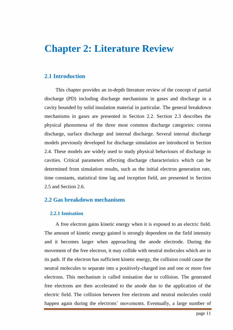
2.2.3 Streamer mechanism
The accumulation of space charges generated from ionisation, i.e. positive
ions and free electrons, is considered in the streamer mechanism. The electric
field between two space charge heads is plotted in Figure 2.1. As can be seen
from Figure 2.1, the field is enhanced in all regions between the electrodes
except the area between the two space charge heads. They generate a local field
which opposes the external electric field E0. During the movement of space
charge heads towards their corresponding electrodes, they gain in size and thus
the electric field is enhanced further in certain regions. When the number of
charge carriers in the avalanche reaches a critical value at which the space charge
field is equal to the external applied field, a streamer is initiated.
Figure 2.1 Diagram representation of external field distortion due to space charge
field [36]
2.3 Partial discharge definition and classification
Partial discharge is defined in IEC 60270 standard [10] as “a localized
electrical discharge that only partially bridges the insulation between conductors
and which may or may not occur adjacent to a conductor”. In other words, it is an
electrical breakdown that does not occur through a complete insulation channel
Chapter 2: Literature Review
page 14
between the electrodes but in a part of it. Partial discharges usually happen in a
very short time (order of nanoseconds) with different levels of magnitude. When
a partial discharge occurs, it is often accompanied by other physical phenomena
such as light, sound, heat emission and chemical reactions [10]. In high voltage
power equipment, the characteristics of partial discharge activity occurring can
be utilised to diagnose the insulation condition of the equipment such as the type
of faults/defects, and stage of aging. Therefore, it is essential to measure partial
discharge activity level.
Partial discharges occur when two conditions are met: a starting electron is
available and the applied voltage exceeds the critical threshold called the
inception voltage. To determine this inception value, the applied voltage is
slowly increased from a low voltage level at which no partial discharges occur
until reaching the voltage level when the first partial discharges are observed
repetitively. On the other hand, the extinction voltage is defined as the voltage
amplitude at which the discharges cease. To determine this value, the applied
voltage is slowly reduced from a higher amplitude at which partial discharges are
occurring to a lower value at which partial discharges disappear completely. The
extinction voltage is generally lower than the inception voltage.
Partial discharges are generally classified into three fundamental categories:
corona discharge, surface discharge and internal discharge [37,39]. These three
partial discharge sub-classes are illustrated in Figure 2.2 [39]. Discharges
occurring in the electrical tree in Figure 2.2c can also be considered as internal
discharge.
2.3.1 Corona discharge
Sharp metal points and edges commonly exist in high voltage conductors of
power equipment due to imperfect manufacturing and finishing. When high
voltage is applied, a significant non-uniform, locally concentrated electric field
appears around these sharp points which could lead to partial breakdown of the
surrounding air. These discharges are defined as corona discharge [36]. Corona
discharges usually happen at high voltage potential. Sharp edges on the ground
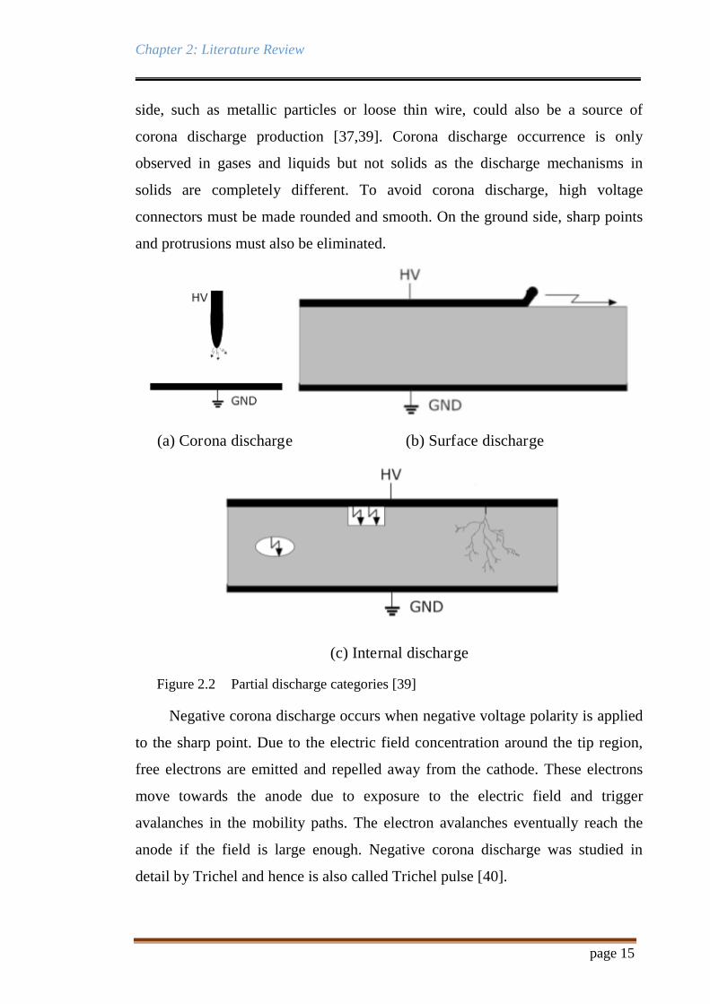
Chapter 2: Literature Review
page 15
side, such as metallic particles or loose thin wire, could also be a source of
corona discharge production [37,39]. Corona discharge occurrence is only
observed in gases and liquids but not solids as the discharge mechanisms in
solids are completely different. To avoid corona discharge, high voltage
connectors must be made rounded and smooth. On the ground side, sharp points
and protrusions must also be eliminated.
(a) Corona discharge (b) Surface discharge
(c) Internal discharge
Figure 2.2 Partial discharge categories [39]
Negative corona discharge occurs when negative voltage polarity is applied
to the sharp point. Due to the electric field concentration around the tip region,
free electrons are emitted and repelled away from the cathode. These electrons
move towards the anode due to exposure to the electric field and trigger
avalanches in the mobility paths. The electron avalanches eventually reach the
anode if the field is large enough. Negative corona discharge was studied in
detail by Trichel and hence is also called Trichel pulse [40].

Chapter 2: Literature Review
page 16
Positive corona discharge occurs when the voltage polarity applied to the
sharp protrusion is positive. It is triggered at a higher voltage amplitude than that
of negative corona discharge since there is no cathode appearance in this case.
Streamers are likely to appear around the tip vicinity when the field is strong
enough. The positive space charges generated from streamers are attracted to the
anode and act like a shield which surrounds the tip region. This shield reduces
the local field around the tip and hence the discharge is stopped. Then the
positive space charges drift away from the sharp point and the corona discharge
reignites due to the reduction of the electric shield. At a higher voltage level,
long streamers develop and cannot be extinguished by positive space charges.
2.3.2 Surface discharge
Surface discharge is a discharge propagating along the interface between
two different insulation materials when a large stress component exists parallel to
the dielectric surface. Figure 2.2b shows that the surface discharge occurs at the
edge of the high voltage electrode and propagates along the solid insulation
surface. Surface discharges are generally observed in high voltage bushings,
cable terminations or the overhang of generator windings [41].
2.3.3 Internal discharge
Solid and liquid dielectrics are usually not completely uniform
(homogeneous) as there are cavities or inclusions within the insulation due to
flaws in the manufacturing processes or in-service conditions. These cavities are
normally gas-filled and have lower electric breakdown strength. Since the
permittivity of the gas in cavities (relative permittivity of ~1) is lower than the
permittivity of surrounding dielectric material, the electric field in cavities is
enhanced and higher than that in the surrounding dielectric. Thus, electrical
breakdown easily occurs in cavities when high voltage is applied. When the
electric stress in the cavity is sufficiently high and exceeds the breakdown
strength of the gas, an internal discharge can be initiated [36,42]. During a partial
discharge, gas contents in the cavity change from a non-conducting to conducting
state, resulting in a decrease of electric stress in a very short time [43].

Chapter 2: Literature Review
page 17
Discharges due to electrical treeing can be also categorised as internal
discharges. Electrical trees can be found in solid insulations such as polymers,
epoxy resins and rubbers.
Consequences of partial discharge activities in a cavity within high voltage
insulation can be very severe as partial discharge could eventually lead to
complete failure of the insulation system. Continuing internal discharge is one of
the main causes of dielectric deterioration and accelerates the electrical treeing
process. Repetition of partial discharges gradually lengthens the electrical trees
due to the progressive decomposition of organic elements. Ultimately, electrical
trees stop growing when tree channels provide a completely conducting path
between the electrodes, with complete breakdown of insulation [44-46].
2.4 Internal discharge model
2.4.1 Three capacitance model
A well-known model to describe a partial discharge encapsulated in an
insulation material is the three capacitance model or ‘abc’ model [36]. A
discharge is simulated by an instantaneous change of charging stage of an
imaginary capacitance represented by the cavity in the dielectric. This model is
widely used to describe the transient behaviours of a discharge activity such as
discharge current, apparent charge magnitude as a function of time due to the
voltage change across the cavity during the discharge. However, this model is not
practical to describe charge movement properties during a discharge as there is
charge accumulation on the cavity surface which makes it not an equipotential
surface [47]. An improvement of this model was made to consider the
accumulated charges on the cavity surface [48]. This model was simulated by
using a variable resistance dependent on time and applied voltage, which
characterises the partial discharge as a cavity changing from a non-conducting
state to a conducting state.
Figure 2.3 illustrates a typical capacitive equivalent circuit of a cavity
surrounded by an insulation material. Here, Ca is essentally the bulk insulation
capacitance of the test object, and Cb represents the capacitance of the healthy

Chapter 2: Literature Review
page 18
dielectric in series with the cavity. The cavity is represented by a capacitance Cc
which is in parallel with a spark gap Fc. Va is the applied voltage on the test
object and Vc is the voltage across the cavity.
V~
Vc
Vb
Va
Ca
Cb
Cc
Fc
(a) characteristics circuit elements
VaCa
Cb
CcFc
ib
ibicic + ib
(b) transient currents flowing through PD equivalent circuit
Figure 2.3 Three capacitance model of partial discharge in a cavity
A partial discharge is assumed to ignite when the voltage dropped across
the cavity, Vc, is larger than the inception voltage, Vinc, and discharge stops when
Vc is lower than the extinction voltage, Vext. In the event of discharge, a combined
transient current between the discharging current in the cavity and the current
through the capacitance Cb flows through the spark gap. The current flowing
through Cb also passes through the object capacitance Ca. These currents are
generated by a sudden drop of voltage across the cavity during the discharge. In
the measurement of partial discharge, it is important to distinguish the internal
charge from the external charge. The internal charge, also called the physical
(true) charge, is calculated by the time integral of the current flowing through the
cavity, which includes ib and ic. The external charge, also known as apparent
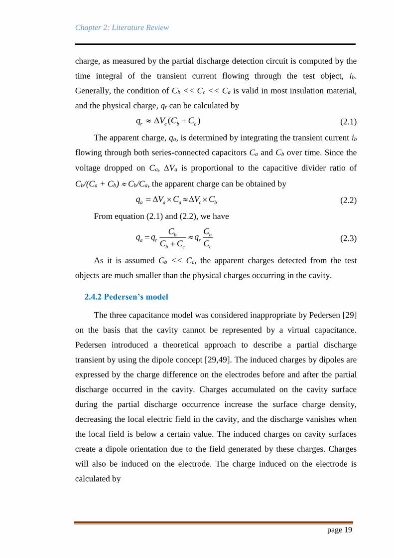
Chapter 2: Literature Review
page 19
charge, as measured by the partial discharge detection circuit is computed by the
time integral of the transient current flowing through the test object, ib.
Generally, the condition of Cb << Cc << Ca is valid in most insulation material,
and the physical charge, qr can be calculated by
( )r c b cq V C C (2.1)
The apparent charge, qa, is determined by integrating the transient current ib
flowing through both series-connected capacitors Ca and Cb over time. Since the
voltage dropped on Ca, Va is proportional to the capacitive divider ratio of
Cb/(Ca + Cb) Cb/Ca, the apparent charge can be obtained by
a a a c bq V C V C (2.2)
From equation (2.1) and (2.2), we have
b b
a r r
b c c
C Cq q q
C C C
(2.3)
As it is assumed Cb << Cc, the apparent charges detected from the test
objects are much smaller than the physical charges occurring in the cavity.
2.4.2 Pedersen’s model
The three capacitance model was considered inappropriate by Pedersen [29]
on the basis that the cavity cannot be represented by a virtual capacitance.
Pedersen introduced a theoretical approach to describe a partial discharge
transient by using the dipole concept [29,49]. The induced charges by dipoles are
expressed by the charge difference on the electrodes before and after the partial
discharge occurred in the cavity. Charges accumulated on the cavity surface
during the partial discharge occurrence increase the surface charge density,
decreasing the local electric field in the cavity, and the discharge vanishes when
the local field is below a certain value. The induced charges on cavity surfaces
create a dipole orientation due to the field generated by these charges. Charges
will also be induced on the electrode. The charge induced on the electrode is
calculated by
Chapter 2: Literature Review
page 20
. .
S
q r dS
(2.4)
where is the dipole moment due to deposited charges on the cavity
surface S, r is the radius vector along the surface S, is the surface charge
density and is a dimensionless scalar function which depends on the space
charge location relative to the electrodes.
If the cavity is either ellipsoidal or spherical, the induced charge q or the
apparent charge from equation (2.4) can be calculated as
0( )inc extq K E E (2.5)
where K is the constant depending on cavity dimensions and geometry, is
the volume of the cavity, is dielectric permittivity, 0 is the Laplace’s equation
solution at the cavity location for material without any cavity [28], Einc is the
inception field and Eext is the extinction field. The boundary conditions used to
solve Laplace’s equation are 0 = 1 at the measured electrode and 0 = 0 at the
other electrode.
The induced charge transient has been investigated by analysing charges
and potential on electrodes just before and after a discharge [28]. It is assumed
that V and Q are the voltage and charge on the electrode before a partial
discharge. After a discharge is finished, the electrode potential drops by a value
of V while the amount of charge on the electrode gains Q, which is the
supplied charge from the external source. As a result, the induced charge q can
be expressed by
q C V Q C V (2.6)
where C is the system capacitance. If the circuit impedance is high relative
to the discharge current, the term Q can be ignored in equation (2.6).
2.4.3 Niemeyer’s model
A partial discharge model based on the streamer type process has been
developed by Niemeyer [31]. This model consists of a mathematical model of
initial electron generation rate, a model of streamer mechanism and the
Chapter 2: Literature Review
page 21
evaluation of partial discharge magnitude. By solving Poisson’s equation, the
electric field in the cavity can be found and the field enhancement in the cavity is
leveraged to gain the field enhancement factor. This factor is used to calculate
the field enhancement due to the external applied field and the field of
accumulated charge on the cavity surface.
This model was used to simulate partial discharge pulses in a spherical
cavity and then compared with measurement results. The initial electron
generation sources were subdivided into surface emission and volume ionisation,
which are associated with detailed equations related to various physical
parameters of the dielectrics.
The real charge magnitude of the partial discharge is determined by
C*UPD, where UPD is the voltage reduction across the cavity during the
discharge event and C is the capacitance of the cavity which is dependent on
cavity geometry [31]. The apparent charge magnitude is calculated as the
induced charge on the measured electrode, which is reliant on cavity location in
the test object, cavity shape and cavity orientation of the applied electric field
[27,28,50].
This model has been simulated and quantitatively compared with
measurement data and it presented a good agreement between simulation and
measurement. A similar discharge model using a comparable method of field
enhancement estimation was used to investigate discharge behaviours in a
spherical cavity embedded in epoxy resin [51]. A stochastic approach has been
used to simulate cavity discharges with a streamer mechanism to analyse effects
of aging on discharge activities [32]. These models have successfully simulated
cavity discharges within material of epoxy resin and produced simulation results
with good agreement to measured data. However, this research was only
conducted at a single value of applied frequency of 50 Hz.
2.4.4 Finite element analysis model
A dynamic electric field-based model has been developed by Forssen to
investigate partial discharge characteristics [52] using finite element analysis
Chapter 2: Literature Review
page 22
(FEA) method. Partial discharge behaviours in a cylindrical cavity surrounded by
a solid dielectric under various applied frequencies have been simulated by this
model. This model was run dynamically and interfaced with a MATLAB code to
calculate partial discharge characteristics. The model includes an insulation
material with a cylindrical cavity inside and two spherical electrodes. A partial
discharge is simulated by an instantaneous change of cavity conductivity during
the discharge from the insulating to conducting state, i.e. increase of cavity
conductivity and the electric field of the whole model is obtained numerically by
using the finite element analysis method. The apparent charge is computed by
integrating the current through the ground electrode over the discharge duration.
The charge decay in the cavity is modelled by the change of cavity surface
conductivity. The simulation results of partial discharge characteristics at
frequency range of 0.01 Hz to 100 Hz were then verified with experimental data
to discuss effects of physical parameters on partial discharge behaviours.
However, this model did not take into account decay mechanisms of space
charges generated after a partial discharge. Illias improved this model to study
partial discharge behaviours in a spherical cavity within a dielectric under
various applied frequencies [35]. The expansion of the partial discharge model in
[35] included the introduction of a charge decay rate via a charge decay time
constant to simulate discharge activities in a spherical void. However, this
research did not investigate partial discharge behaviours at very low frequency of
0.1 Hz, and the charge decay constant was assumed to be independent of applied
voltage amplitudes and frequencies.
2.5 Initial electron generation rate
One of the conditions of partial discharge inception is that an initial starting
electron must be available to initiate the electron avalanche [36]. Free electrons
generated within a cavity are generally from two main sources: surface emission
and volume ionisation [18,31].
Chapter 2: Literature Review
page 23
2.5.1 Surface emission
Surface emission is an electron generation mechanism in which free
electrons are generated from the cavity surface under the effects of electric stress
and temperature. Free electrons are mainly from an electron detrapping process
of shallow traps near or on the cavity surface, injected electrons from electrodes,
electrons accumulated on the cavity surface after a discharge and electrons
emitted from ionised impact processes. Under ongoing partial discharge pulses,
electrons emitted from the cavity surface are the main sources of free electrons
[16,22]. The surface-emitted electron rate is further enhanced by increasing the
electric stress or the temperature in the cavity [54]. The initial electron generation
rate is strongly dependent on the applied voltage level, insulation material
characteristics and the geometry and location of the cavity within the dielectric.
Electron avalanches can be developed along the void surface which is
parallel to the local electric field. When a free electron is released from the cavity
surface due to photoionisation, the ionised process of electrons can be triggered
along the cavity wall. Thus, the electron avalanche developed from this process
may cause free electrons to be deposited with high density on a small area of the
cavity surface. This results in a similar amount of positive charges trapped at the
material region where accumulated electrons exist. This phenomenon usually
occurs in a relatively narrow cavity which is parallel to the applied field.
2.5.2 Volume ionisation
Volume ionisation is a process under which free electrons are emitted by
radiative gas ionisation between energetic photons and gas molecules [55]. As a
result, free electrons are generated from the detachment of electrons and positive
ions. This ionisation rate is dependent on gas pressure, gas volume exposed to the
volume ionisation and gas contents. Volume ionisation is the main source of
initial free electrons in a virgin cavity which has never been exposed to partial
discharge occurrence as the electron detrapping energy required from the unaged
cavity surface is generally higher than that in an aged cavity [31]. Moreover, a

Chapter 2: Literature Review
page 24
free electron can be generated by the photoionisation mechanism, where gas
molecules absorb photons with sufficient energy to release electrons.
2.6 Parameters affecting partial discharge activity
Partial discharge characteristics in a cavity within a solid dielectric are
generally affected by the applied electric stresses and cavity conditions. The
electric stress characteristics influencing partial discharge activities include the
magnitude, waveform and frequency of applied voltage [17,18,33,56,57]. Cavity
conditions that affect partial discharge characteristics are the size and shape of
cavity, cavity location within the insulation and gas parameters in the cavity such
as humidity and pressure [58-61]. Physical parameters with effects on partial
discharge activities are time constants related to charge transport and decay rate,
the statistical time lag and the inception field.
2.6.1 Time constants
Free charges generated from a partial discharge are accumulated on the
cavity surface and will decay with time [14,19-20]. These charges can decay via
charge recombination in the cavity, charge conduction along the cavity surface,
charge diffusion into deeper traps on the cavity surface or charge neutralisation
by gas ions in the cavity. The charge decay rate is controlled by several physical
time constants such as cavity surface time constant, s, the effective charge decay
time constant, decay, and the material time constant, mat [18,31,33]. These time
constants have a significant effect on partial discharge characteristics such as
partial discharge magnitude level and phase distribution.
Free charges generated after a partial discharge event are deposited on the
cavity surface and are able to move freely along the cavity surface via charge
conduction. During this movement, these charges have a possibility of
recombination when they meet with opposite sign charges, resulting in a decrease
in the amount of free charges. This decay rate is regulated by the cavity surface
time constant, s, which is strongly dependent on the cavity surface conductivity,
s [19,28-30,32]. The higher the value of s is, the faster the charge movement is,
Chapter 2: Literature Review
page 25
resulting in higher chances of charge recombination. Therefore, the initial
electron generation rate is reduced between two consecutive discharges [18].
Cavity surface conductivity is increased after long exposure to repetitive
discharges due to chemical deterioration and aging conditions [63,65]. If the
cavity surface time constant s is smaller than the period of applied voltage, the
charge decay via cavity surface conduction is substantial.
A certain amount of charges accumulated on the cavity surface will be
trapped in shallow traps on the surface. These charges may diffuse into deeper
traps in the cavity surface, or may diffuse further into the bulk insulation material
after a certain time. The rate of this movement can be assigned a charge decay
time constant, decay [31-32,51]. A shorter time constant reflects a faster rate of
charge transport process from shallow traps into deeper traps. If this time
constant decay is smaller than the time period of applied voltage, it means there is
a considerable surface charge transport into deeper traps. Consequently, the
surface emission of electrons is reduced but the local electric field in the cavity is
hardly changed as these charges still have a contribution to the surface charge
field. However, electrons in deeper traps are less likely to contribute to igniting a
partial discharge than those trapped in shallow traps.
Surface charges left on the cavity wall after a partial discharge event may
also diffuse into the bulk insulation via volume conduction because, realistically,
the material always has a finite value of conductivity. Hence, the amount of free
charges accumulated on the cavity surface may decrease with time. The rate of
surface charge diffusion via this charge transport process is determined by the
material time constant, mat [22], which is obviously dependent on the material
conductivity. A relatively long time constant mat indicates a slow charge decay
rate, which hardly changes the local electric field and the number of free
electrons and vice versa. In fact, the time constant mat is considerable compared
with the period of applied voltage in this thesis due to the very low conductivity
of the material used in partial discharge experiments, and thus this charge decay
process is fairly slow and can be ignored in its contribution to partial discharge
activities.

Chapter 2: Literature Review
page 26
2.6.2 Statistical time lag
Two conditions must be fulfilled to incept a partial discharge: the electric
field in the cavity must exceed the inception value and a free electron must be
available to ignite an electron avalanche. When the local electric field in the
cavity is higher than the inception value, Einc, there may not be a starting electron
to initiate a discharge. Such a case would have a time delay for partial discharge
occurrence when the inception threshold is exceeded. The average time delay
between the instant the inception field is exceeded and the moment a partial
discharge occurs is called the statistical time lag, stat [31,33]. Because of stat,
partial discharges usually occur at electric stress larger than the inception value.
As the electron generation rate varies with stress conditions, the statistical
time lag is strongly dependent on the frequency and amplitude of the applied
voltage. At high frequency, time intervals between consecutive discharges are
relatively small, thus fewer free charges vanish after a partial discharge event. As
a result, there are more charges available for the following discharge. Therefore,
the electron generation rate is higher and the next partial discharge may be
incepted immediately when the electric field exceeds the critical value, thus
decreasing the statistical time lag. On the other hand, fewer free charges are
available after a discharge at low frequency as more free charges are likely to
decay due to relatively long time intervals between consecutive partial
discharges. Therefore, the electron generation rate is smaller when the following
partial discharge is expected to happen. It is a reason for longer statistical time
lag as partial discharges may not occur immediately after the inception value is
exceeded [66]. Regarding amplitude dependence, stat is likely to decrease with
the increase of applied voltage level as free electron emission is enhanced at a
higher applied voltage.
The statistical time lag can differ between successive partial discharges.
The waiting time for the first partial discharge could be longer than that of
following discharges within the same applied voltage cycle. A cavity which has
not yet been exposed to partial discharge occurrence lacks free electrons as
sources of available electrons are limited. However, there are abundant free
Chapter 2: Literature Review
page 27
charges generated after the first partial discharge is incepted which act as the
main source of free electrons for the following partial discharges. Therefore, the
waiting time of free electrons for subsequent partial discharges is reduced and
shorter than the first partial discharge. As the accumulated charges on the cavity
surface decay in time, the number of charges ready for the next partial discharge
decreases. Thus, the time delay between consecutive partial discharges is
dependent on the charge decay rate and free electron availability [32].
2.6.3 Inception field
The inception value of the electric field is the minimum field in the cavity
required for a discharge to ignite. This value for partial discharges with the
streamer process in a cavity is dependent on many parameters such as cavity
geometry, pressure, material permittivity, ionisation mechanisms and the gap
between two electrodes [31,32,51,66]. The value of the inception field for
streamer type partial discharge could be calculated by
1
( )inc n
cr
E BE p
p pd
(2.7)
where cr
E p , B and n are parameters related to the gas ionisation process,
p is the pressure in the void and d is the cavity diameter. For air, these parameters
are cr
E p = 24.2 VPa-1m-1, n = 0.5 and B = 8.6 Pa1/2 [28,31,36].
2.7 Conclusion
This chapter reviewed literature related to partial discharge, especially
corona discharge and internal discharge in cavities. Physical mechanisms leading
to partial discharge were discussed in detail. To date, several well-known models
have been developed to simulate discharges in cavities: the th ree capacitance
model, Pedersen’s model and finite element analysis based model. The
advantages and drawbacks of these simulation models were discussed. These
models provide a practical approach for studying cavity discharges within a solid
insulation material to identify critical physical parameters affecting discharge
behaviours. The parameters of significance include the statistical time lag, charge
Chapter 2: Literature Review
page 28
decay time constant and inception field. The availability of initial electrons also
influences discharge characteristics. The following chapter presents the
development of an improved approach built on the finite element analysis based
model. This new approach involves a minimal set of adjustable parameters and
adaptable charge decay time constant depending on applied frequency.

page 29
Chapter 3: Modelling of Internal
Discharge
3.1 Introduction
The partial discharge model proposed in this thesis is an improvement of
the finite element analysis (FEA) model developed by previous researchers
[35,52]. The proposed model involves a minimal set of adjustable parameters: the
number of free electrons generated at inception field, number of free electrons
due to volume ionisation and surface charge decay constant which is adopted to
applied frequency. This model is built in a finite element method based software,
i.e. COMSOL Multiphysics, and interconnected with MATLAB program
language to simulate discharges in a cylindrical cavity embedded in a solid
dielectric material. The modelling of partial discharge is described in detail
together with governing equations. Sections in this chapter cover model creation
and settings in COMSOL, cavity discharge process simulation, model of initial
electron generation rate and flow charge of partial discharge simulation. In order
to reduce the simulation time, several assumptions proposed in the model to
simplify the work are explained thoroughly. The advantage of this improved
model over the previous work is also discussed.
The developed model has been tested under various conditions of applied
stress in terms of voltage amplitudes and frequencies. The obtained simulated
data are then compared with measurement results to identify critical parameters
affecting the discharge process in the cavity at different stress conditions. The
determined critical parameters are the field inception and extinction, charge
decay constant and conductivity of the cavity surface. Physical phenomena
considered to directly influence discharge activities are the charge conduction
along cavity surfaces and the initial electron generation rate.

Chapter 3: Modelling of Internal Discharge
page 30
3.2 Finite Element Method model
The model was developed in symmetric two-dimensional (2D) axis of finite
element method (FEM) based software, i.e. COMSOL Multiphysics, and was
interfaced with MATLAB program language. The electric field and electric
potential in the model are solved by using partial differential equations. Two-
dimensional symmetric geometry of the model was chosen to reduce the
simulation time as fewer meshing elements required to solve the finite element
method in the software were employed during the calculation. In the COMSOL
environment, the physics of “electric currents” are used to solve the electric field
and potential distribution in the model.
3.2.1 Field model equation
The distribution of electric potential in the model is governed by several
mathematical equations. The fundamental equations of the field model are:
fD (3.1)
0
ffJ
t
(3.2)
where equation (3.1) is the field equation from Gauss’ law, and equation
(3.2) is the current continuity equation [67]. In these equations, D is the electric
displacement (flux density), f is the free charge density and fJ is the free
current density. Since D E and E V where is the material
permittivity, E is the electric field and V is the electric potential, equation (3.1)
can be rewritten as
)( fV (3.3)
As fJ E , by substituting equation (3.3) into equation (3.2), it can be
expressed as follows
( ) ( ) 0V V
t
(3.4)
where is the material electrical conductivity.

Chapter 3: Modelling of Internal Discharge
page 31
Equation (3.4) is solved by using the finite element method in order to
determine the electric potential distribution in the field model.
3.2.2 Model geometry and meshing
Details of the test sample model geometry developed in the simulation
software are shown in Figure 3.1. The model is a homogeneous solid dielectric
material with a thickness of 3.0 mm and radius of 25 mm. A cylindrical void with
1 mm radius and 1 mm height is introduced at the centre of symmetrical axes
(horizontal r-axis and vertical z-axis) to represent a cavity embedded completely
inside a solid insulation material. The cavity surface of 0.1 mm is also created to
simulate the charge mobility on the cavity wall. The upper electrode is applied
with sinusoidal voltage at various frequencies whilst the lower electrode is
always grounded. A meshing method with 2D unstructured triangular elements is
used. The resolutions of cavity and cavity surface meshes are set at “fine” in the
software as higher accuracy of field calculation is needed within these areas. The
model meshing is shown in Figure 3.2.
High voltage electrode
Dielectric Material
Void surface
Ground Electrode
Cylindrical void
Symmetric axis
Figure 3.1 The axial-symmetric 2D model
3.2.3 Boundary and domain settings
Assigned constants, sub-domain settings and boundary settings of the
model used for simulation are summarised in Table 3.1 to Table 3.3. Boundary
line settings in the model are shown in Figure 3.3. In Table 3.3, n is the normal
vector to a boundary and J is the total current density.
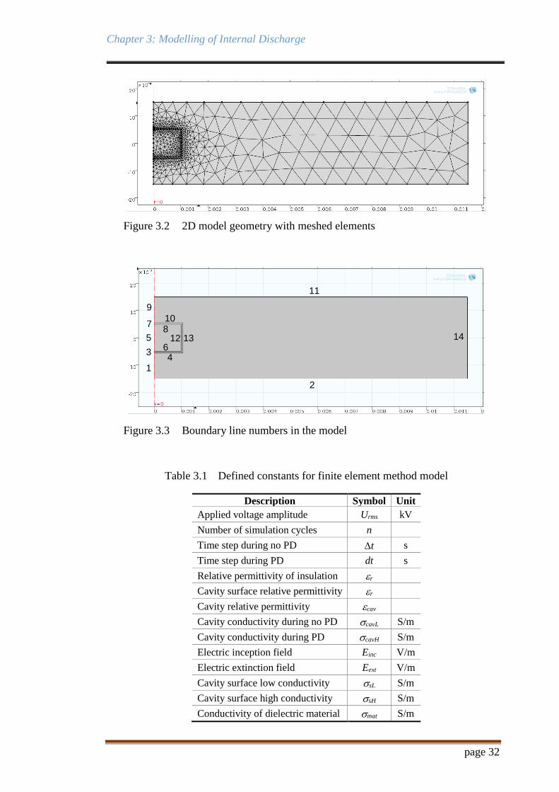
Chapter 3: Modelling of Internal Discharge
page 32
Figure 3.2 2D model geometry with meshed elements
1
2
34
56
12
11
107
8
9
13 14
Figure 3.3 Boundary line numbers in the model
Table 3.1 Defined constants for finite element method model
Description Symbol Unit
Applied voltage amplitude Urms kV
Number of simulation cycles n
Time step during no PD t s
Time step during PD dt s
Relative permittivity of insulation r
Cavity surface relative permittivity r
Cavity relative permittivity cav
Cavity conductivity during no PD cavL S/m
Cavity conductivity during PD cavH S/m
Electric inception field Einc V/m
Electric extinction field Eext V/m
Cavity surface low conductivity sL S/m
Cavity surface high conductivity sH S/m
Conductivity of dielectric material mat S/m
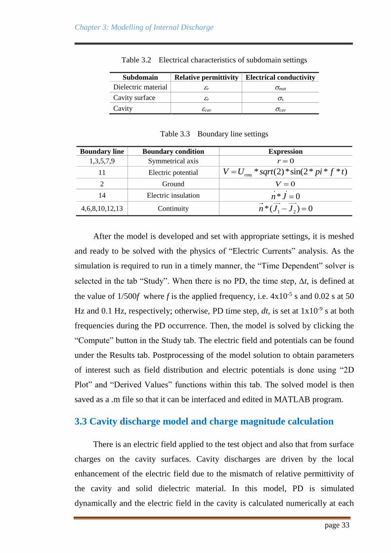
Chapter 3: Modelling of Internal Discharge
page 33
Table 3.2 Electrical characteristics of subdomain settings
Subdomain Relative permittivity Electrical conductivity
Dielectric material r mat
Cavity surface r s
Cavity cav cav
Table 3.3 Boundary line settings
Boundary line Boundary condition Expression
1,3,5,7,9 Symmetrical axis 0r
11 Electric potential * (2)*sin(2* * * )rmsV U sqrt pi f t
2 Ground 0V
14 Electric insulation * 0n J
4,6,8,10,12,13 Continuity 1 2*( ) 0n J J
After the model is developed and set with appropriate settings, it is meshed
and ready to be solved with the physics of “Electric Currents” analysis. As the
simulation is required to run in a timely manner, the “Time Dependent” solver is
selected in the tab “Study”. When there is no PD, the time step, t, is defined at
the value of 1/500f where f is the applied frequency, i.e. 4x10⁻⁵ s and 0.02 s at 50
Hz and 0.1 Hz, respectively; otherwise, PD time step, dt, is set at 1x10⁻⁹ s at both
frequencies during the PD occurrence. Then, the model is solved by clicking the
“Compute” button in the Study tab. The electric field and potentials can be found
under the Results tab. Postprocessing of the model solution to obtain parameters
of interest such as field distribution and electric potentials is done using “2D
Plot” and “Derived Values” functions within this tab. The solved model is then
saved as a .m file so that it can be interfaced and edited in MATLAB program.
3.3 Cavity discharge model and charge magnitude calculation
There is an electric field applied to the test object and also that from surface
charges on the cavity surfaces. Cavity discharges are driven by the local
enhancement of the electric field due to the mismatch of relative permittivity of
the cavity and solid dielectric material. In this model, PD is simulated
dynamically and the electric field in the cavity is calculated numerically at each
Chapter 3: Modelling of Internal Discharge
page 34
time step by solving the partial differential equation via the finite element
method. From the simulation results, the electric field distribution is symmetrical
along the r and z-axes. Hence, the assumption that there is symmetry of electric
field and charge distribution in the cavity along both axes can be made before
and after a PD occurrence. As a result, this can be done in the finite element
method model by assuming that discharges occur in the whole cavity.
In order to reduce the simulation time, there are several assumptions to
simplify the finite element method model developed. Firstly, details of PD
mechanisms, such as the mobility of free electrons and ions during the
propagation of electron avalanches in the cavity, are not included in detail. This
electron avalanche phenomenon has a considerable impact on cavity surface
characteristics after each PD event but it is difficult to determine the physical
parameters related to the cavity surface itself. Instead, a discharge is assumed to
occur in the whole cavity. In the model, this assumption can be made by
changing the conductivity of the whole cavity during PD occurrence.
Secondly, it is assumed that cavity discharges have the characteristics of
streamer discharges. Streamer propagation in air by charge carriers under the
influence of drift and diffusion has been modelled in previous research [68].
Partial discharge development has also been simulated by using particle
modelling, which studies the particle dynamics during the discharge process [69].
However, details of streamer mechanisms are not simulated in this work as the
parameters of interest for PD are charge magnitude and phase only. Hence, a PD
event is assumed to influence the whole cavity when it occurs along the void
symmetrical axis. As a result, an instantaneous electric field is extracted at the
centre of the cavity in the model and it is only dependent on time.
3.3.1 Cavity conductivity
When discharges are simulated dynamically, a discharge occurrence can be
illustrated by changing the physical state of the cavity from a non-conducting to
conducting condition as PD is assumed to affect the whole cavity. This can be
done by increasing the cavity conductivity from its initial value when there is no

Chapter 3: Modelling of Internal Discharge
page 35
PD occurrence, to a higher conductivity value during the PD activity. When the
cavity conductivity is increased, it causes the electric field in the cavity to drop
continuously within discharge duration. When the field is below the extinction
value, the discharge event stops and cavity conductivity recovers to its initial
state, or non-conducting condition. The value of cavity conductivity during the
conducting state, i.e. during a PD process, can be estimated via electron
conductivity in plasma as conductivity due to ions is assumed to be insignificant.
In [70], the electron conductivity in plasma, e, can be computed by using
2
e e ee
e e
N
m c
(3.5)
where e is the coefficient related to electron energy distribution and mean
free path, me is the mass of the electron, e is the electron mean free path, ce is
the electron thermal velocity and Ne is the electron density, which can be
calculated as
34 3
e
q eN
r (3.6)
where q/e is the number of electrons in the streamer channel, q is total
charge in the streamer channel, e is the electric charge of the electron and r is the
cavity radius. During the PD process, the current flow through the cavity, Icav(t)
increases from zero to a certain maximum value while the electric field begins to
decrease. Then, the current Icav(t) starts to drop while the cavity field Ecav(t) keeps
decreasing. A PD ceases when the cavity field drops below the extinction field,
Eext. After the PD event stops, the cavity conductivity, cav, is reset to its initial
value and the cavity current disappears.
3.3.2 Discharge magnitude
An advantage of this model is that PD charge magnitudes can be calculated
numerically as discharges are modelled dynamically. From the solved model in
COMSOL, it is possible to calculate the real and apparent charge for each PD
event by integrating the current flowing through the cavity and through the
ground electrode, over the discharge time duration, that is
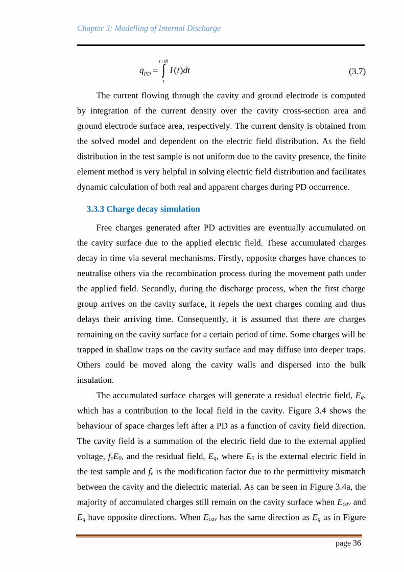
Chapter 3: Modelling of Internal Discharge
page 36
( )
t dt
PD
t
q I t dt
(3.7)
The current flowing through the cavity and ground electrode is computed
by integration of the current density over the cavity cross-section area and
ground electrode surface area, respectively. The current density is obtained from
the solved model and dependent on the electric field distribution. As the field
distribution in the test sample is not uniform due to the cavity presence, the finite
element method is very helpful in solving electric field distribution and facilitates
dynamic calculation of both real and apparent charges during PD occurrence.
3.3.3 Charge decay simulation
Free charges generated after PD activities are eventually accumulated on
the cavity surface due to the applied electric field. These accumulated charges
decay in time via several mechanisms. Firstly, opposite charges have chances to
neutralise others via the recombination process during the movement path under
the applied field. Secondly, during the discharge process, when the first charge
group arrives on the cavity surface, it repels the next charges coming and thus
delays their arriving time. Consequently, it is assumed that there are charges
remaining on the cavity surface for a certain period of time. Some charges will be
trapped in shallow traps on the cavity surface and may diffuse into deeper traps.
Others could be moved along the cavity walls and dispersed into the bulk
insulation.
The accumulated surface charges will generate a residual electric field, Eq,
which has a contribution to the local field in the cavity. Figure 3.4 shows the
behaviour of space charges left after a PD as a function of cavity field direction.
The cavity field is a summation of the electric field due to the external applied
voltage, fcE0, and the residual field, Eq, where E0 is the external electric field in
the test sample and fc is the modification factor due to the permittivity mismatch
between the cavity and the dielectric material. As can be seen in Figure 3.4a, the
majority of accumulated charges still remain on the cavity surface when Ecav and
Eq have opposite directions. When Ecav has the same direction as Eq as in Figure
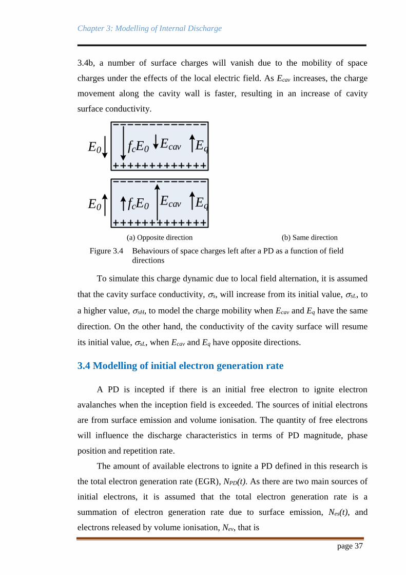
Chapter 3: Modelling of Internal Discharge
page 37
3.4b, a number of surface charges will vanish due to the mobility of space
charges under the effects of the local electric field. As Ecav increases, the charge
movement along the cavity wall is faster, resulting in an increase of cavity
surface conductivity.
EqEcavE0 fcE0
EqEcavE0 fcE0
(a) Opposite direction (b) Same direction
Figure 3.4 Behaviours of space charges left after a PD as a function of field
directions
To simulate this charge dynamic due to local field alternation, it is assumed
that the cavity surface conductivity, s, will increase from its initial value, sL, to
a higher value, sH, to model the charge mobility when Ecav and Eq have the same
direction. On the other hand, the conductivity of the cavity surface will resume
its initial value, sL, when Ecav and Eq have opposite directions.
3.4 Modelling of initial electron generation rate
A PD is incepted if there is an initial free electron to ignite electron
avalanches when the inception field is exceeded. The sources of initial electrons
are from surface emission and volume ionisation. The quantity of free electrons
will influence the discharge characteristics in terms of PD magnitude, phase
position and repetition rate.
The amount of available electrons to ignite a PD defined in this research is
the total electron generation rate (EGR), NPD(t). As there are two main sources of
initial electrons, it is assumed that the total electron generation rate is a
summation of electron generation rate due to surface emission, Nes(t), and
electrons released by volume ionisation, Nev, that is
Chapter 3: Modelling of Internal Discharge
page 38
( ) ( )PD es evN t N t N (3.8)
As discharges are assumed to occur along the symmetrical axis, the electron
generation rate due to surface emission Nes(t) is dependent on time only.
It is assumed that free electrons due to surface emission are mainly from
detrapping charges from the shallow traps on the cavity surface. Hence, the
amount of these charges is strongly dependent on the local electric field in the
cavity. To simplify the model, a simple equation is introduced to calculate the
number of free electrons due to surface emission as follows
( )( ) cav
es
inc
E tN t N
E (3.9)
where N is the number of free electrons generated at the inception field Einc,
and Ecav(t) is the local electric field in the cavity at a time t. A similar equation
has been introduced in [33] to represent the dependence of electron generation on
the applied voltage. Equation (3.9) is motivated by the Richardson-Schottky law
[31] because many of the material parameters in the Richardson-Schottky law are
difficult to quantify. Thus, this equation aims to simulate an acceptable field
dependence of electron generation rate instead of describing a detailed physical
model with a number of unknown parameters.
After a PD occurrence, free electrons generated during the discharge
process decay in time via the previously mentioned mechanisms such as charge
recombination and diffusion into deeper traps. Hence, these decayed charges are
assumed to no longer contribute to the initial electron generation rate to trigger
the following discharge when it is likely to occur. This decay rate is determined
by a charge decay time constant, decay. It is assumed that charges decay
exponentially with time. The term of charge decay time constant, decay, has been
introduced successfully in previous research [19,71-72], to model the
disappearance rate of free charges accumulated on the cavity surface. Moreover,
the electron generation rate due to surface emission has been stated as a function
of increasing electric field after a discharge [27,48-49]. It is assumed that this is
exponentially dependent on the ratio of the cavity electric field and inception
field. As a result, equation (3.9) can be rewritten as
Chapter 3: Modelling of Internal Discharge
page 39
( ) ( )( ) exp expcav cavPD
es
inc decay inc
E t E tt tN t N
E E
(3.10)
where tPD is the moment the previous discharge occurred and (t-tPD) is the
time elapsed from the previous discharge. Hence, equation (3.8) can be expressed
in full to illustrate the total initial electron generation rate as
( ) ( )( ) exp expcav cavPD
PD ev
inc decay inc
E t E tt tN t N N
E E
(3.11)
In this equation, the three constants, i.e. N, decay and Nev, are freely
adjustable to fit the simulation data with measurement results.
A PD is incepted when two conditions are met: the local electric field
exceeds the inception value and a starting electron is available. The free electron
condition is dependent on the electron generation rate. Due to the stochastic
nature of PD activities, a probability approach is used to determine the likelihood
of PD occurrence. The possibility of PD occurrence, P(t), is calculated when the
cavity field Ecav(t) is larger than inception value Einc. P(t) can be determined by
( ) ( )PDP t N t t (3.12)
where t is the time interval of calculation. P(t) is then compared with a
random number R between 0 and 1. A PD will only occur when P(t) is larger
than R. A discharge will always be incepted if P(t) is larger than 1.
3.5 Simulation flowchart in MATLAB
3.5.1 Parameters for simulation
Table 3.4 shows the parameters used for all simulations in this work. The
number of simulated voltage cycles is 500. This allows sufficient PD
characteristics to be obtained from the simulation for analysis at both very low
frequency and power frequency. As can be seen in this table, the time step of
simulation is chosen as 1/500f when there is no PD occurrence, where f is the
frequency of applied voltage. This value guarantees the simulation time is an
acceptable time span while keeping good precision results of the electric field at
each time step. If the chosen t is too short, the total simulation time would be
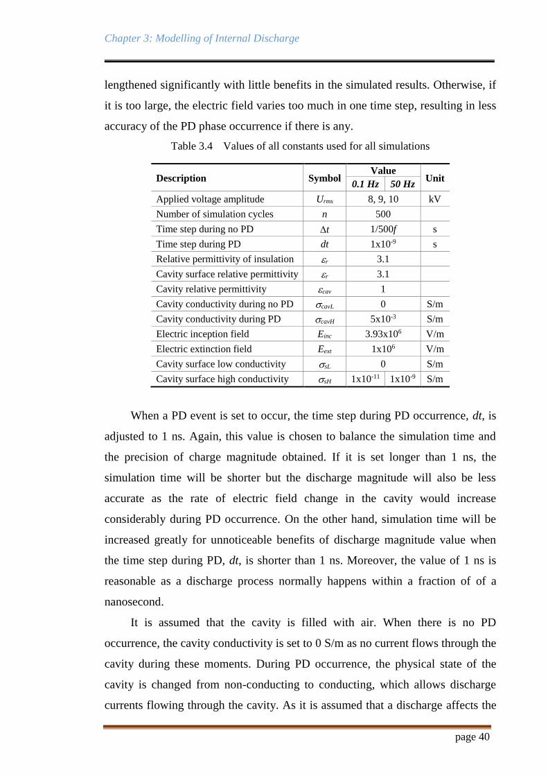
Chapter 3: Modelling of Internal Discharge
page 40
lengthened significantly with little benefits in the simulated results. Otherwise, if
it is too large, the electric field varies too much in one time step, resulting in less
accuracy of the PD phase occurrence if there is any.
Table 3.4 Values of all constants used for all simulations
Description Symbol Value
Unit 0.1 Hz 50 Hz
Applied voltage amplitude Urms 8, 9, 10 kV
Number of simulation cycles n 500
Time step during no PD t 1/500f s
Time step during PD dt 1x10⁻⁹ s
Relative permittivity of insulation r 3.1
Cavity surface relative permittivity r 3.1
Cavity relative permittivity cav 1
Cavity conductivity during no PD cavL 0 S/m
Cavity conductivity during PD cavH 5x10⁻³ S/m
Electric inception field Einc 3.93x10⁶ V/m
Electric extinction field Eext 1x10⁶ V/m
Cavity surface low conductivity sL 0 S/m
Cavity surface high conductivity sH 1x10-11 1x10⁻⁹ S/m
When a PD event is set to occur, the time step during PD occurrence, dt, is
adjusted to 1 ns. Again, this value is chosen to balance the simulation time and
the precision of charge magnitude obtained. If it is set longer than 1 ns, the
simulation time will be shorter but the discharge magnitude will also be less
accurate as the rate of electric field change in the cavity would increase
considerably during PD occurrence. On the other hand, simulation time will be
increased greatly for unnoticeable benefits of discharge magnitude value when
the time step during PD, dt, is shorter than 1 ns. Moreover, the value of 1 ns is
reasonable as a discharge process normally happens within a fraction of of a
nanosecond.
It is assumed that the cavity is filled with air. When there is no PD
occurrence, the cavity conductivity is set to 0 S/m as no current flows through the
cavity during these moments. During PD occurrence, the physical state of the
cavity is changed from non-conducting to conducting, which allows discharge
currents flowing through the cavity. As it is assumed that a discharge affects the

Chapter 3: Modelling of Internal Discharge
page 41
whole cavity, the conductivity of the cavity, cav, is set equal to 5x10⁻³ S/m
during the PD process. This value is reasonable to keep the simulation time short
enough while ensuring the cavity field does not decrease too fast during a
discharge. If cav is chosen higher than 5x10⁻³ S/m, the cavity field will drop
significantly in a short time and the discharge will be stopped at a field level
much lower than the extinction value, resulting in a much larger PD charge
magnitude. On the other hand, if cav is set lower than 5x10⁻³ S/m, it is found that
simulation time increases greatly while there are unnoticeable changes of
simulation results.
The thickness of the cavity surface layer is set equal to 0.1 mm. Several
values around this choice were trialled, which showed that the difference of
electric field distribution in the model with various cavity surface thicknesses is
quite small. The simulation time also increased considerably if this thickness was
set too small, i.e. lower than 0.1 mm, as many more meshing elements were
required to solve the model.
The relative permittivity of the insulation material, r, is determined from
the measurement of test samples in the laboratory using dielectric frequency
response analysis in the range from 0.1 Hz to 50 Hz. This value of 3.1 is
acceptable because the relative permittivity of Acrylonitrile-Butadiene-Styrene, a
type of thermoplastic resin, is within the range of 2.8 to 3.2 found in the literature
[75]. The cavity surface permittivity is set equal to r as it is considered a part of
the solid insulation material. The cavity relative permittivity, cav, is set to 1 as it
is assumed the cavity is filled with air.
The simulation value of the inception field, Einc, is calculated from equation
(2.7), which results in 3.93x10⁶ V/m. The value of the extinction field, Eext,
should be lower than the inception field and is chosen based on the minimum
measured discharge. If this value is set too high, it will cause the discharge to
occur within a shorter time, which results in less discharge magnitude. On the
other hand, discharge will happen for a long time which increases the discharge
magnitude if Eext is set too low. After experimenting with numerous values, it
was found that Eext is equal to 1x10⁶ V/m for all simulations.

Chapter 3: Modelling of Internal Discharge
page 42
It is assumed that surface charges do not decay when the cavity field Ecav
and residual field Eq have opposite directions. Thus, the initial value of cavity
surface conductivity, sL, is set equal to 0 S/m in both cases of applied
frequencies. When Ecav and Eq have the same direction, sH is equal to 1x10⁻⁹
S/m at frequency of 50 Hz and 1x10-11 S/m at very low frequency. These values
were determined after numerous trials to fit the simulated PD repetition rate with
the measurement results.
In equation (3.11), the values of N, decay and Nev are freely adjustable to fit
the simulation results with measured data. As these parameters are dependent on
applied frequency and voltage amplitude, their values would be different in
various scenarios. By applying trial and error procedures to minimise differences
with the expected values, the values of N, decay and Nev have been determined as
shown in Table 3.5 and are described in detail in Chapter 7 for comparison
between simulation and measurement results.
Table 3.5 Values of adjustable parameters for simulation
Frequency
(Hz)
Applied voltage
(kV) N
decay
(ms) Nev
0.1
8 30 1000 2
9 15 800 3
10 30 800 3
50
8 2500 2 40
9 2500 2 50
10 3500 2 50
3.5.2 Program flowchart
A loop program was developed in MATLAB programming language to
determine all simulation parameters and interface with the finite element method
model to solve the electric field distribution. The program includes iterations
over time, probability determination of a discharge event, calculation of
discharge characteristics such as charge magnitude, phase occurrence and
discharge duration, calculation of initial electron generation rate and post-
processing of simulation results. Flowcharts of the main code, solving the finite

Chapter 3: Modelling of Internal Discharge
page 43
element method model at each time step and PD occurrence determination, are
shown in Figure 3.5 to Figure 3.7.
Start
Model initialised
Increase time step End time?
Update boundary
and subdomain
Ecav > Einc ?
Calculate P
P > R ?
cav cavH
Solve FEM model
Ecav < Eext ?
Eq/Ecav > 0
s sL
s sH
cav cavL
Save results
EndY
Y
Y
Y
N
N
N
N
Solve FEM model
N
Y
Figure 3.5 Main flowchart in MATLAB
Input
Mapping current solutions
to extended mesh
Update subdomain and
boundary settings
Solve FEM model
Output
Figure 3.6 Flowchart of “Solve FEM model” at each time step

Chapter 3: Modelling of Internal Discharge
page 44
P > R
Input
Calculate electron
generation rate, NPD(t)
Compute probability P
Generate random
number R
Output
Discharge is
set to occur
No discharge
occurs
Update subdomain and
boundary settings
Y N
Figure 3.7 Flowchart of PD occurrence determination
Initially, the MATLAB workspace was cleared to ensure there are no
foreign variables affecting the simulation process. Then, all constants, variables
and parameters required for simulation were initialised to predefined values as
well as the dimensions of the test object and the cavity. The applied frequency,
voltage amplitude and number of simulated cycles were also determined in this
step.
Next, the finite element method model was created with input parameters
defined in the previous steps. The model geometry was then meshed and
boundary settings were chosen with values that have been assigned. After all
settings and the sub-domain were set, the model was solved with initial
conditions to give the necessary data, such as electric field and potential
distribution, required to commence the main loop.

Chapter 3: Modelling of Internal Discharge
page 45
After that, the main loop was launched. The MATLAB code interacts with
the finite element method model to update the boundary and sub-domain settings
at each time step. The electric field and potential distribution were extracted from
the solved model at each time step to update the settings for the next time step
and determine the likelihood of PD occurrence. The electric field in the cavity,
Ecav was regularly compared with the inception value Einc. If Ecav was larger than
Einc, the probability calculation of PD occurrence was triggered. The total initial
electron generation rate was computed and then the likelihood of a PD event was
calculated using equation (3.12). Then, P(t) was compared with a random
number R in the range from 0 to 1. If P(t) was larger than R, a discharge was
assumed to happen. If not, the no-discharge condition still remained and the loop
moved on to the next time step.
When a discharge occurrence is determined, the distribution of the electric
field and equipotential lines in the model just before and after the first two PDs is
saved. In general, solved models at any time step can be saved providing that
they are predefined before running the main program. In this work, the solved
models of the first two discharges were chosen due to interest in the surface
charge effect on the local electric field distribution just before and after the
discharge. For the first PD, it is assumed that no surface charges existed in the
cavity before discharge occurrence.
After the first PD, surface charges accumulated on the cavity surface have a
considerable influence on the field distribution before the second PD occurrence.
During the discharging state, the conductivity of the cavity was increased to the
predefined value as mentioned above. Boundary and sub-domain settings were
updated to solve the model with discharge occurrence conditions. The time step
was changed to 1 ns and the electric field and flown current in the cavity were
extracted continuously from the model at each time step to calculate the
discharge magnitude during the PD. Discharge was set to stop when Ecav was
lower than the extinction value, Eext. When the discharge ceased, the cavity
conductivity returned to its initial value and the main loop moved on to the next

Chapter 3: Modelling of Internal Discharge
page 46
time step. The discharge magnitude and phase of occurrence for the
corresponding discharge were saved in the MATLAB workspace.
The main loop of program continued to run until the predefined number of
voltage cycles was reached. The discharge phase and magnitude of all PDs
occurring during the simulation were saved and then analysed. From these
parameters, the phase-resolved PD patterns at simulated applied voltage and
frequency can be plotted and compared with measurement results from
experiments. Details of PD patterns are described further in Chapter 4.
3.6 Conclusion
This chapter described the development of a model of partial discharge
occurring in a cavity surrounded by solid dielectric material, using a combined
software platform of COMSOL interfaced with MATLAB. The physical
behaviours of partial discharge were explained in detail with mathematical
equations and how the finite element method model represents each physical
phenomenon accordingly. The advantages of this model are:
1. With the help of the finite element method, the electric field and potential
distribution in any void geometry within a solid insulation material can be
obtained at any time related to the discharge moment, i.e. before, during and after
the discharge.
2. Discharge events can be simulated dynamically. Moreover, real and
apparent discharge magnitudes can be calculated numerically from currents
flowing through the cavity and through the ground electrode, correspondingly
during the discharge activity under excitation of very low frequency and power
frequency.
3. The distribution of electric field and potential in the material can be
plotted graphically which gives an insight into pre-discharge processes.
4. The conduction of accumulated surface charges along the cavity can be
simulated by varying the conductivity of the cavity surface under various
frequency excitations.

Chapter 3: Modelling of Internal Discharge
page 47
The next chapter describes the preparation of the real test samples modelled
in this chapter. The experimental setup including the partial discharge
measurement system and how measurements were performed are also explained.
page 48
Chapter 4: Test Setup and Partial
Discharge Measurements
4.1 Introduction
In this chapter, partial discharge measurement setups in the laboratory are
presented in detail to explain how to detect different types of discharges, i.e.
corona discharges and internal discharges in cavities, using an IEC 60270 [10]
compliant testing circuit. The instruments and components required for the
measurement circuit are introduced in Section 4.2. The raw discharge data
recorded from measurements are extracted for further analysis via phase-resolved
partial discharge (PRPD) analysis. A set of parameters for characterising
discharge behaviour are presented in Section 4.3. The design and fabrication of
test objects to produce discharges is described in Section 4.4. Section 4.5
explains the discharge measurement procedures at various stress conditions to
ensure that obtained experimental data are consistent and accurate.
4.2 Partial discharge measurement setup
The partial discharge experiments of this research were conducted in the
UNSW High Voltage laboratory. A partial discharge measurement circuit fully
compliant with specifications in IEC 60270 Standard was used as shown in
Figure 4.1. The main components of the measuring circuit comprise a variable
high voltage power source, blocking capacitor Ck, test object Cx and a measuring
impedance Z which is part of the quadripole unit (CPL542). The detailed PD
measurement setups in the laboratory are shown in Figure 4.2 and Figure 4.3. For
variable frequency high voltage power source, an arbitrary function generator
(Agilent Keysight HB35000B) was connected to a high voltage amplifier (Trek
20/20C-HS). This function generator is able to generate various waveforms at

Chapter 4: Test Setup and Partial Discharge Measurements
page 49
low voltage, including preset and user customised defined signals. The high
voltage amplifier is capable of amplifying the input signal with a gain of 2000
and able to produce maximum voltage amplitude of 20 kV. Specifications of the
function generator and high voltage amplifier are provided in Appendix A. The
blocking capacitor has a value of 1.1 nF and discharge-free up to 50 kV.
The PD measurement device is an Mtronix Advanced Partial Discharge
Analysis System MPD600. The measuring impedance Z is placed in the coupling
unit CPL542 which is connected in series with the blocking capacitor. The
captured PD and applied voltage signals are sent from the coupling unit to the
acquisition unit MPD600. Here, the measured data are converted to optical
signals and then transmitted via optical fibres to the controller MCU502. Finally,
the raw data are converted back to digital electrical signals and transferred to the
computer via a USB interface.
Figure 4.1 Circuit setup for partial discharge measurement [76]
The fundamental purpose of the PD measurement circuit is to measure the
transient current pulse flowing through the test object when a discharge occurs.
During a PD occurrence, the voltage across the test object is momentarily
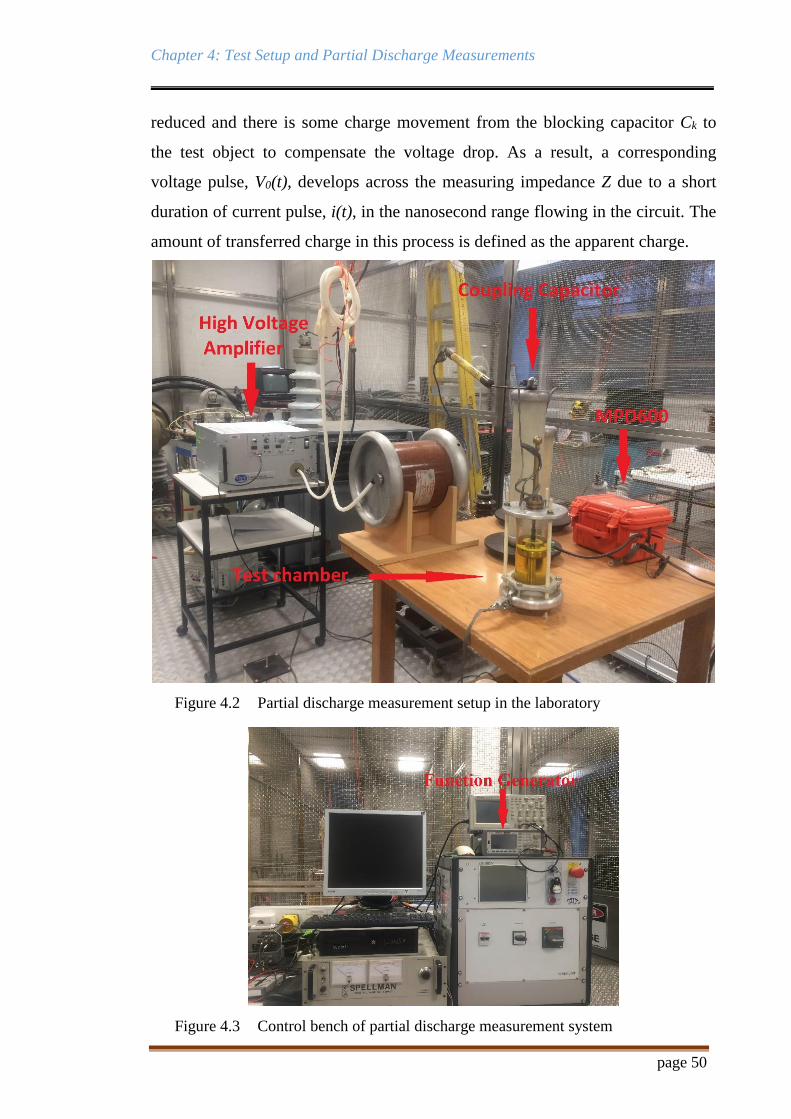
Chapter 4: Test Setup and Partial Discharge Measurements
page 50
reduced and there is some charge movement from the blocking capacitor Ck to
the test object to compensate the voltage drop. As a result, a corresponding
voltage pulse, V0(t), develops across the measuring impedance Z due to a short
duration of current pulse, i(t), in the nanosecond range flowing in the circuit. The
amount of transferred charge in this process is defined as the apparent charge.
Figure 4.2 Partial discharge measurement setup in the laboratory
Figure 4.3 Control bench of partial discharge measurement system
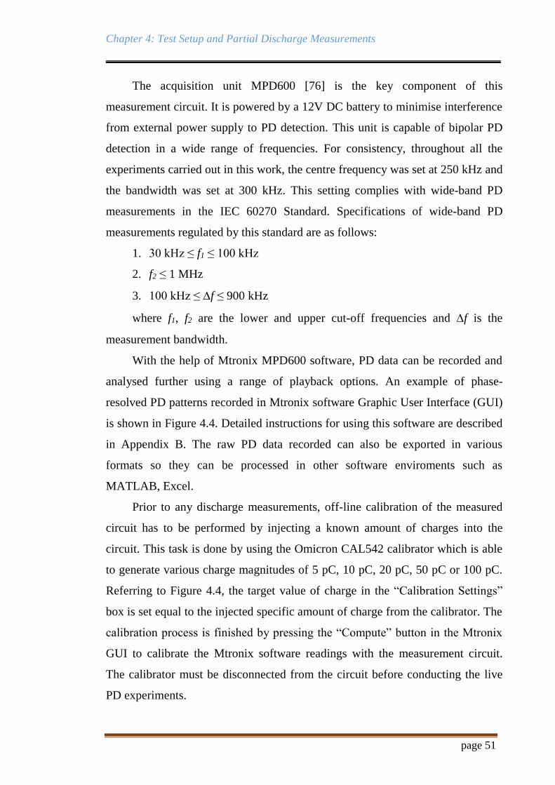
Chapter 4: Test Setup and Partial Discharge Measurements
page 51
The acquisition unit MPD600 [76] is the key component of this
measurement circuit. It is powered by a 12V DC battery to minimise interference
from external power supply to PD detection. This unit is capable of bipolar PD
detection in a wide range of frequencies. For consistency, throughout all the
experiments carried out in this work, the centre frequency was set at 250 kHz and
the bandwidth was set at 300 kHz. This setting complies with wide-band PD
measurements in the IEC 60270 Standard. Specifications of wide-band PD
measurements regulated by this standard are as follows:
1. 30 kHz ≤ f1 ≤ 100 kHz
2. f2 ≤ 1 MHz
3. 100 kHz ≤ f ≤ 900 kHz
where f1, f2 are the lower and upper cut-off frequencies and f is the
measurement bandwidth.
With the help of Mtronix MPD600 software, PD data can be recorded and
analysed further using a range of playback options. An example of phase-
resolved PD patterns recorded in Mtronix software Graphic User Interface (GUI)
is shown in Figure 4.4. Detailed instructions for using this software are described
in Appendix B. The raw PD data recorded can also be exported in various
formats so they can be processed in other software enviroments such as
MATLAB, Excel.
Prior to any discharge measurements, off-line calibration of the measured
circuit has to be performed by injecting a known amount of charges into the
circuit. This task is done by using the Omicron CAL542 calibrator which is able
to generate various charge magnitudes of 5 pC, 10 pC, 20 pC, 50 pC or 100 pC.
Referring to Figure 4.4, the target value of charge in the “Calibration Settings”
box is set equal to the injected specific amount of charge from the calibrator. The
calibration process is finished by pressing the “Compute” button in the Mtronix
GUI to calibrate the Mtronix software readings with the measurement circuit.
The calibrator must be disconnected from the circuit before conducting the live
PD experiments.
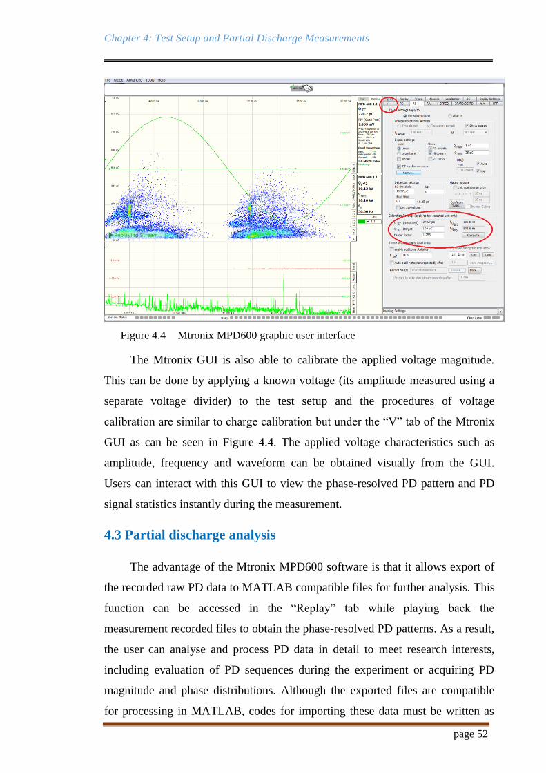
Chapter 4: Test Setup and Partial Discharge Measurements
page 52
Figure 4.4 Mtronix MPD600 graphic user interface
The Mtronix GUI is also able to calibrate the applied voltage magnitude.
This can be done by applying a known voltage (its amplitude measured using a
separate voltage divider) to the test setup and the procedures of voltage
calibration are similar to charge calibration but under the “V” tab of the Mtronix
GUI as can be seen in Figure 4.4. The applied voltage characteristics such as
amplitude, frequency and waveform can be obtained visually from the GUI.
Users can interact with this GUI to view the phase-resolved PD pattern and PD
signal statistics instantly during the measurement.
4.3 Partial discharge analysis
The advantage of the Mtronix MPD600 software is that it allows export of
the recorded raw PD data to MATLAB compatible files for further analysis. This
function can be accessed in the “Replay” tab while playing back the
measurement recorded files to obtain the phase-resolved PD patterns. As a result,
the user can analyse and process PD data in detail to meet research interests,
including evaluation of PD sequences during the experiment or acquiring PD
magnitude and phase distributions. Although the exported files are compatible
for processing in MATLAB, codes for importing these data must be written as
Chapter 4: Test Setup and Partial Discharge Measurements
page 53
these files use binary format for storing the numerical values. Thus, MATLAB
scripts have been written to import and post-process PD data to investigate PD
characteristics obtained from the measurement results. The common discharge
characteristics to be investigated are the PD repetition rate (the number of PDs
per cycle or per second), maximum and average discharge magnitudes and PD
phase distribution.
4.3.1 Basic discharge quantities
The basic parameters related to each single record discharge ith are as
follows:
– apparent discharge magnitude: qi, in pico-coulombs (pC)
– discharge polarity: pi, positive or negative
– phase position (in relation to the AC voltage cycle): i, in degrees
– moment of occurrence (relative to the start of test): ti, in seconds
Since PD phenomena are complicated and exhibit stochastic behaviour,
these basic quantities show strong statistical inconsistency. Hence, it is not
realistic to interpret PD characteristics based merely on any single discharge for
diagnosis of dielectric conditions. This has led to the introduction of integrated
discharge parameters to analyse PD activities. These integrated parameters are
derived from basic quantities. They provide the general trend of discharge
behaviour over a predefined number of AC voltage cycles [39]. These integrated
values are specified in [10] in detail and summarised as follows:
1. Average discharge current I – the summation of all absolute magnitudes
of apparent charge in a given period of time T divided by that period,
specified in amperes (A) or coulombs per second (C/s).
1
1 n
i
i
I qT
(4.1)
2. Discharge repetition rate r – the average number of PD events over a
given period of time T or a given number of AC cycles K, expressed in
pulses per second (pps) or pulses per cycle (ppc).
Chapter 4: Test Setup and Partial Discharge Measurements
page 54
nr
T (4.2)
nr
K (4.3)
3. Discharge power P – the average power injected into test object
terminals due to apparent discharge over a given period of time T,
specified in watts (W).
1
1 n
i i
i
P q vT
(4.4)
4. Quadratic rate D – the summation of the square of each apparent
discharge magnitude qi over a given period of time T divided by that
period, specified in coulombs square per second (C2/s).
2
1
1 n
i
i
D qT
(4.5)
where n is the total number of discharge pulses in the given period of time
T, vi is the instantaneous value of applied voltage at the occurrence moment of
discharge qi.
Other integrated parameters associated with the apparent discharge
magnitude qi are:
1. Maximum discharge magnitude qmax – the largest magnitude of all
apparent charges recorded in a given duration of time T, expressed in
coulombs (C).
qmax = max[q1, q2, ….., qn] (4.6)
2. Average discharge magnitude qave – the average magnitude of all
apparent charges recorded in a given duration of time T, expressed in
coulombs (C).
1
1 n
ave i
i
q qn
(4.7)
4.3.2 Pulse sequence analysis
Pulse sequence analysis is a method to examine partial discharge
phenomena by evaluating the sequence of individual PDs in terms of the
Chapter 4: Test Setup and Partial Discharge Measurements
page 55
relationship between two consecutive PD events [77]. The voltage difference and
the time interval between these sequential PD events are used to investigate the
‘memory’ effects of a preceding PD event on the following PD activity. These
effects are attributed to space charges accumulated after the first discharge,
especially in a case of solid dielectric material. The resultant voltage difference
patterns provide another way to characterising PD behaviour. The drawback is
that it does not exploit the phase information and more importantly, the main
concern is that it does not directly account for the effect of the discharge
magnitude. For insulation diagnostics, the discharge magnitude is always the
most important parameter. Therefore, this research is focused only on the more-
commonly used phase-resolved pattern analysis.
4.3.3 Phase-resolved partial discharge analysis
One of the most common techniques used to analyse PD data is phase-
resolved partial discharge analysis (PRPDA), which has been applied by many
researchers [35,52,78-88]. It is often used to investigate PD patterns related to
AC voltage at 50 Hz frequency. This technique was developed further to measure
PD activities at various applied frequencies [56]. In general, PRPDA equipment
detects the apparent discharge magnitude and occurrence phase of each single
partial discharge and the phase-resolved pattern is obtained by arranging and
counting single discharge magnitude, qi, happening at the phase i regarding the
AC voltage cycle in a two-dimensional (2D) data array. Then, the phase-resolved
PD pattern is acquired by mapping all discharge parameters, including discharge
magnitude and occurrence phase, over a number of recorded voltage cycles into a
representative single cycle. The occurrence phase of discharges is characterised
in X channels which are in the range of 0 to 360. The discharge magnitudes are
characterised in Y channels, with half of them for positive discharges and the
other half for negative discharges [35]. The mapping process of discharge
characteristics into XY channels is shown in Figure 4.5. The value of C(n, qm) is
the counted number of discharges occurring at phase n with discharge
magnitude qm.

Chapter 4: Test Setup and Partial Discharge Measurements
page 56
Figure 4.5 Partial discharge characteristics mapping process [35]
In a 2D phase-resolved PD pattern plot, the x-axis represents the phase
channels while the y-axis illustrates the discharge magnitude channels. All
discharges are mapped onto this graph with corresponding discharge magnitude
and occurrence phase. The number of discharges with the same magnitude and
occurrence phase, i.e. C(n, qm), is displayed in this graph with different colour,
where the larger number of discharge events is represented by higher colour
intensity. Figure 4.6 shows an example of a phase-resolved PD pattern obtained
from the experiment. The advantage of this pattern is that discharge magnitude
and occurrence phase of each PD can be seen visually in the graph. Thus, partial
discharge analysis based on 2D phase-resolved PD patterns is used in this thesis
to discuss discharge behaviours under various applied frequencies. The analysis
aims to obtain integrated quantities for each single phase window and plot them
against the phase coordinate .
Figure 4.6 Example of a 2D phase-resolved PD pattern

Chapter 4: Test Setup and Partial Discharge Measurements
page 57
4.4 Test object preparation
4.4.1 Test object to produce corona discharge
To generate corona discharges under high voltage application, a needle and
bowl configuration was used as shown in Figure 4.7. The brass bowl has a
hemispherical geometry with a radius of 25 mm whereas the needle has a tip
radius of 61.88 m. The whole setup is housed inside an airtight chamber made
from perspex material. The insulation medium between the needle and the bowl
is air. Corona discharge is ignited when the electric field around the needle tip
exceeds the breakdown strength of air. The common configuration of corona
discharge testing is to apply high voltage to the needle while the bowl is
grounded. The reverse testing is to connect high voltage to the hemispherical cup
while the needle is connected to earth.
25 mm radius
Hemispherical brass
electrode
(a) Configuration layout (b) Test object in the laboratory
Figure 4.7 Test setup for generating corona discharges
To calculate the inception voltage of this configuration, the electrodes can
be considered as two concentric spheres with radius r for the needle tip and
radius R for the hemisphere. The air in the vicinity of the needle tip experiences
breakdown over a distance d as in Figure 4.8 when the voltage across this
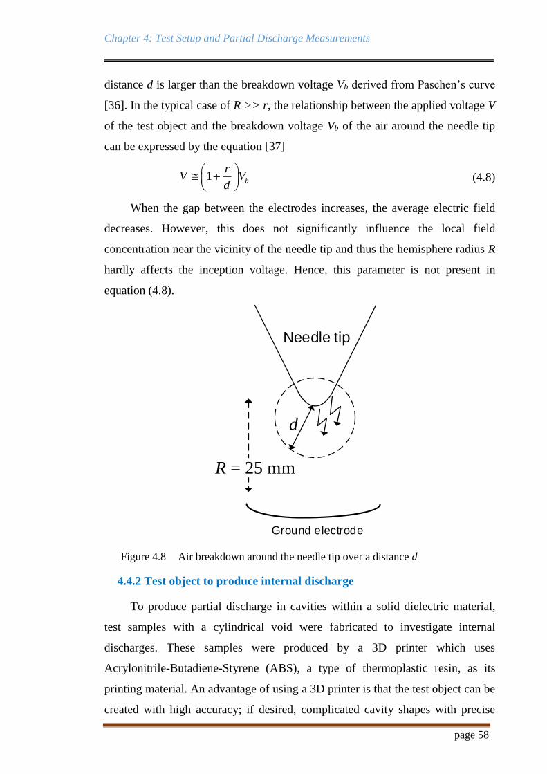
Chapter 4: Test Setup and Partial Discharge Measurements
page 58
distance d is larger than the breakdown voltage Vb derived from Paschen’s curve
[36]. In the typical case of R >> r, the relationship between the applied voltage V
of the test object and the breakdown voltage Vb of the air around the needle tip
can be expressed by the equation [37]
1 b
rV V
d
(4.8)
When the gap between the electrodes increases, the average electric field
decreases. However, this does not significantly influence the local field
concentration near the vicinity of the needle tip and thus the hemisphere radius R
hardly affects the inception voltage. Hence, this parameter is not present in
equation (4.8).
d
Needle tip
Ground electrode
R = 25 mm
Figure 4.8 Air breakdown around the needle tip over a distance d
4.4.2 Test object to produce internal discharge
To produce partial discharge in cavities within a solid dielectric material,
test samples with a cylindrical void were fabricated to investigate internal
discharges. These samples were produced by a 3D printer which uses
Acrylonitrile-Butadiene-Styrene (ABS), a type of thermoplastic resin, as its
printing material. An advantage of using a 3D printer is that the test object can be
created with high accuracy; if desired, complicated cavity shapes with precise

Chapter 4: Test Setup and Partial Discharge Measurements
page 59
dimensions inside the solid test sample can be designed and manufactured. In this
study, the test sample geometry was disc-shaped with a diameter of 50 mm and
thickness of 3 mm. The cylindrical cavity was designed to be at the centre with
diameter of l mm, height of 1 mm and distance of 1 mm from the top and bottom
surfaces of the sample. The cavity was filled with air as it was printed under
normal ambient conditions. The schematic diagram is shown in Figure 4.9. In
this thesis, test samples with four values of cavity diameter l were fabricated and
tabulated in Table 4.1.
3 mm1 mm1 mm1 mm
50 mm
l
Figure 4.9 Test object dimensions
Table 4.1 Test sample properties
Sample 1 2 3 4
l (mm) 2 4 6 8
Figure 4.10 shows an example of a test sample used in this research. The
test sample was sandwiched between two brass electrodes with curvature on their
edges to reduce field concentration when high voltage is applied. This
configuration was held tightly by a mechanical arrangement and fully submerged
in mineral oil (standard transformer oil) in a test cell to prevent unwanted surface
discharges as shown in Figure 4.11.
Figure 4.10 An example of a test object to generate internal discharge
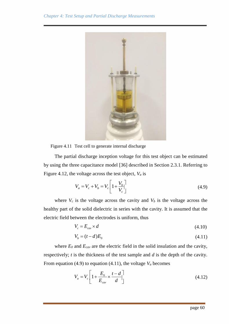
Chapter 4: Test Setup and Partial Discharge Measurements
page 60
Figure 4.11 Test cell to generate internal discharge
The partial discharge inception voltage for this test object can be estimated
by using the three capacitance model [36] described in Section 2.3.1. Referring to
Figure 4.12, the voltage across the test object, Va is
1 b
a c cb
c
VV V V V
V
(4.9)
where Vc is the voltage across the cavity and Vb is the voltage across the
healthy part of the solid dielectric in series with the cavity. It is assumed that the
electric field between the electrodes is uniform, thus
c cavV E d (4.10)
0( )bV t d E (4.11)
where E0 and Ecav are the electric field in the solid insulation and the cavity,
respectively; t is the thickness of the test sample and d is the depth of the cavity.
From equation (4.9) to equation (4.11), the voltage Va becomes
01a c
cav
E t dV V
E d
(4.12)

Chapter 4: Test Setup and Partial Discharge Measurements
page 61
It is assumed that the cavity is filled with air since the test object was
fabricated in normal conditions. Since the electric displacement is the same in the
cavity and the solid dielectric, the electric field in the cavity can be expressed as:
0cav rE E (4.13)
where r is the relative permittivity of the dielectric. By substituting
equation (4.13) into equation (4.12), the voltage across the cavity is
11
ac
r
VV
t d
d
(4.14)
For convenience, an empirical formula for Paschen’s curve of air at 20C is
used to determine the breakdown voltage Vbreakdown [36] in the cavity
6.72 24.36( )breakdownV pd pd (4.15)
At room temperature of 20C and normal pressure in the cavity which is not
too small (pd > 0.1 bar.mm), equation (4.15) is used to calculate the breakdown
voltage in the cavity [39]. From equation (4.14) and (4.15), the inception voltage
for the test samples can be estimated.
V~
Vc
Vb
Va
Ca
Cb
Cc
td
A
Figure 4.12 Electrical discharge in the cavity and its equivalent circuit
4.5 Measurement methods
4.5.1 Pre-measurement
It is essential to ensure that there are no air bubbles in the mineral oil
(trapped under the flat electrode) since discharges occurring in these bubbles
cause interference to measurement results when applying high voltage. Sharp
edges were also eliminated in metallic mechanical supporting elements to avoid
Chapter 4: Test Setup and Partial Discharge Measurements
page 62
unwanted corona discharges. Before conducting the experiments, the setup was
tested without the corona discharge test cell and also with the internal discharge
test cell using a dummy test sample of same dimension but with no internal
cavity. This is to ensure the whole system was partial discharge free at the
desired working voltage. It was found to be free of partial discharge up to 19
kVpeak. Any higher voltage level was not tested since the maximum output of
the high voltage amplifier is limited at 20 kVpeak and the actual voltage level
used to stress the test specimens was below 15 kV.
In the measurement of corona and internal discharges, the voltage at which
the first discharge appears may not be the actual inception value when a new test
object is used. With the first high voltage application, there may be a time delay
for discharge to occur in test objects. This is due to the lack of free electrons to
trigger electron avalanches around the needle tip area or in the cavity, especially
for a virgin cavity which has never been exposed to partial discharge before.
Consequently, test objects were pre-excited with a high voltage level below the
estimated inception value for 30 minutes at 50 Hz frequency, that is 2 kV for
corona discharges and 6 kV for internal discharges, before conducting the
discharge measurements.
After the pre-excitation process, the high voltage amplitude applied to the
test object was increased in steps of 100 V after every two minutes until the
discharges were detected repetitively by the measurement device at a certain
voltage level and that level of voltage was recorded as the inception voltage
value (note that applying too fast a rate of voltage rise is likely to cause over-run
and thus inaccurate inception voltage). The applied voltage was then increased to
the desired value for recording partial discharge data.
4.5.2 Corona discharge measurements at different temperatures
For corona discharge measurements at different temperatures, the test
object was placed in an oven in which the ambient temperature was monitored by
a thermocouple as can be seen in Figure 4.13. This forms part of the thermostat
control system which operates the switching of the heating element to regulate

Chapter 4: Test Setup and Partial Discharge Measurements
page 63
the temperature. The oven temperature was very stable during the data
acquisition period. Experiments were conducted at four different temperature
settings: 20C, 30C, 35C and 40C.
An optical fibre temperature sensor (ASEA 1010) was inserted into the test
chamber. Note that with this fibre sensor (instead of conventional thermocouple
wire), it was possible to position the sensor close to the electrode tip of the test
object to record the ambient air temperature during the test. The thermostat
control system and optical fibre temperature monitor equipment are shown in
Figure 4.14. High voltage from the supply outside was connected to the test cell
via a bushing through the oven wall (top side). The test chamber was airtight and
the oven door was also completely closed during the whole test experiment
series. Thus, the humidity level in the test chamber was expected to remain
constant at all times and assumed to be approximately equal to normal room
conditions.
Figure 4.13 Corona discharge setup for variable air temperature measurements
Chapter 4: Test Setup and Partial Discharge Measurements
page 64
4.5.3 Discharge measurements at various applied frequencies
The test object was stressed at high voltage amplitude continuously at
various applied frequencies to measure corona discharges and cavity internal
discharges. For corona discharge testing, the determination of inception voltage
was carried out by slowly increasing the applied voltage amplitude until the first
discharge appeared after the pre-excitation period at 50 Hz frequency. The
voltage level was kept constant for a period of 5 minutes for recording discharge
data at inception value. Then the applied voltage was increased to a higher level
which was then left for another 5 minutes before starting discharge measurement.
This process helped achieve a steady, regular discharge activity. Once the
measurements under 50 Hz frequency were finished, the applied voltage was
reduced slowly to the initial value which was at the pre-excited stage. The
applied frequency was then decreased slowly to the very low frequency range
which was 0.1 Hz, 0.08 Hz and 0.05 Hz while high voltage was still applied to
test object. Under the excitation of each very low frequency level, the applied
voltage was kept unchanged for another 30 minutes before increasing the voltage
level to determine the inception value. This period of time was to ensure the
charge mobility had become steady under the new frequency application and to
minimise the memory effects of applied frequency on discharge behaviours.
Another 30 minutes was given at each measured voltage level before recording
the stable corona discharge data. The total test time to record all discharge data at
all applied frequencies was around 8 hours. For each type of measurement
presented in Chapter 5, the test procedures were repeated three times for
consistency of results.
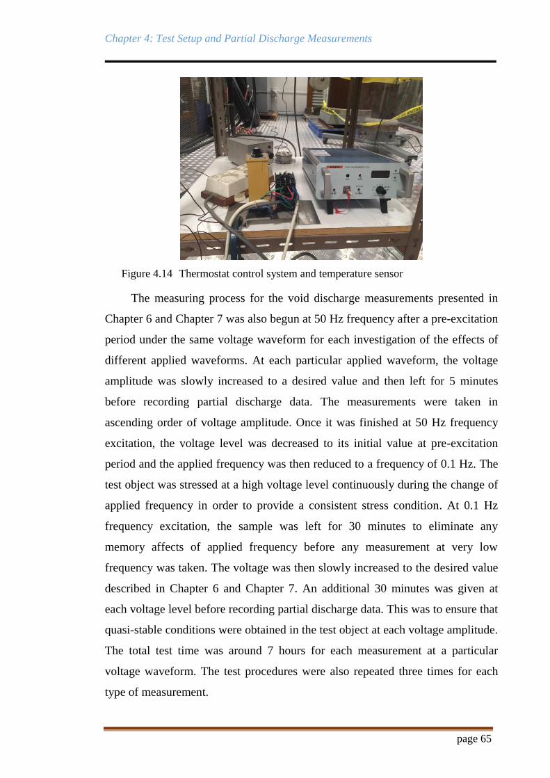
Chapter 4: Test Setup and Partial Discharge Measurements
page 65
Figure 4.14 Thermostat control system and temperature sensor
The measuring process for the void discharge measurements presented in
Chapter 6 and Chapter 7 was also begun at 50 Hz frequency after a pre-excitation
period under the same voltage waveform for each investigation of the effects of
different applied waveforms. At each particular applied waveform, the voltage
amplitude was slowly increased to a desired value and then left for 5 minutes
before recording partial discharge data. The measurements were taken in
ascending order of voltage amplitude. Once it was finished at 50 Hz frequency
excitation, the voltage level was decreased to its initial value at pre-excitation
period and the applied frequency was then reduced to a frequency of 0.1 Hz. The
test object was stressed at a high voltage level continuously during the change of
applied frequency in order to provide a consistent stress condition. At 0.1 Hz
frequency excitation, the sample was left for 30 minutes to eliminate any
memory affects of applied frequency before any measurement at very low
frequency was taken. The voltage was then slowly increased to the desired value
described in Chapter 6 and Chapter 7. An additional 30 minutes was given at
each voltage level before recording partial discharge data. This was to ensure that
quasi-stable conditions were obtained in the test object at each voltage amplitude.
The total test time was around 7 hours for each measurement at a particular
voltage waveform. The test procedures were also repeated three times for each
type of measurement.

Chapter 4: Test Setup and Partial Discharge Measurements
page 66
4.6 Conclusion
This chapter described preparation of the test objects used to produce
corona discharges and cavity discharges in this thesis. A needle and bowl
configuration was used to generate corona discharge under variable applied
frequencies and at different ambient temperatures controlled by appropriate
hardware setup. For void discharges, test samples with a cylindrical cavity of
accurate dimension within the solid dielectric were fabricated for partial
discharge measurements under various stress conditions, such as voltage
waveforms, voltage amplitudes and applied frequencies. An Omicron MPD 600
commercial system fully compliant with the IEC 60270 standard was used to
record measurements. Individual partial discharge events were captured for
analysis. Discharge characteristics are quantified in terms of the phase-resolved
patterns, the discharge repetition rate, maximum and average discharge
magnitudes. The measurement results of corona discharges and cavity discharges
under different applied frequency excitation are presented and analysed in
Chapter 5 and Chapter 6, correspondingly. A comparison between measurement
and simulation results of void discharges at different applied voltage amplitudes
under very low frequency and power frequency excitation is described in Chapter
7. This allows key parameters influencing partial discharge characteristics at
different applied frequencies to be determined.
page 67
Chapter 5: Corona Discharge
Activities: Effects of Applied Voltage
Waveforms and Ambient Conditions
5.1 Introduction
In this chapter, corona discharge behaviours at two applied frequencies of
0.1 Hz and 50 Hz are presented and analysed. Two different applied voltage
waveforms, traditional sine wave and square wave, were used to stress the test
object at various voltage amplitude levels. A hybrid AC-DC voltage waveform
was also used to further investigate the effects of voltage waveforms on corona
discharge characteristics at different applied frequencies. Corona discharge
measurements were performed at various ambient temperatures to observe how
ambient conditions influence discharge behaviours at very low frequency and
power frequency.
To generate corona discharges, a test object of a point and bowl electrode
configuration in air was used. This test object was described in detail in Chapter
4 and summarised here. It is a brass cup of hemispherical geometry with a radius
of 25 mm, and the needle has a tip radius of 61.88 m. The insulating medium
between the needle and the bowl is ambient air. The effects of applied voltage
waveforms such as sine wave, square wave and hybrid AC-DC wave on corona
discharge at different frequencies are reported in Section 5.2. Section 5.3
presents the effects of ambient temperatures on corona discharge characteristics.
Chapter 5: Corona Discharge Activities: Effects of Applied Voltage Waveforms and
Ambient Conditions
page 68
5.2 Effects of applied waveform on corona discharge
5.2.1 Corona discharge at different applied frequencies under excitation
of sinusoidal waveform
In this section, a traditional sine wave was applied to the test object. The
high voltage source was connected to the needle and the bowl was grounded. The
partial discharge inception voltage (PDIV) was determined by gradually
increasing the applied voltage level in steps of 100 V until corona discharges
were detected steadily in the partial discharge measurement system described in
Chapter 4. At inception voltage, corona discharges only occur around the peak of
the negative half-cycle (270o phase angle) as shown in Figure 5.1 and Figure 5.2.
The phase-resolved partial discharge patterns were recorded for the same
duration of 3 minutes in order to compare the repetition rate. Such a pattern is
well known and can be explained. Electrons are injected from the negative
electrode. Under the applied electric field, these negatively-charged electrons
move to the positive electrode. On the way, they collide with other gas
molecules, cause ionisation and release more free electrons which results in an
exponential increase in the number of electrons (i.e. electron avalanches) and
hence electrical discharge.
In the negative voltage half-cycle, the needle tip is at negative potential and
the very high stress at the tip accelerates the injected electrons to produce an
avalanche. In contrast, in the positive half-cycle, the bowl is at negative potential.
Because the electric field near the round surface is more uniform and less
enhanced than the field near a sharp point (i.e. needle) [36], free electrons can
hardly be injected into the air and thus the absence of PDs in the positive half-
cycle. However, if the applied voltage is increased much further, the resultant
electric field increase will also cause PDs in the positive half-cycle.
An interesting observation when comparing Figure 5.1 and Figure 5.2 is
that, under very low frequency, the PDs tend to lag and occur slightly away from
the peak of the negative voltage half-cycle. Also, their magnitudes are not as

Chapter 5: Corona Discharge Activities: Effects of Applied Voltage Waveforms and
Ambient Conditions
page 69
uniform as those cases of higher frequencies which have a distinct cone shape
instead of a flat distribution.
Under the applied frequency in the 10 to 50 Hz range, the PDIV was found
to be different. At 50 Hz and 40 Hz, the PDIV was 2.6 kV while at 30 Hz, 20 Hz
and 10 Hz, it was progressively higher at 2.8 kV, 3.0 kV and 3.5 kV,
respectively. As expected, with higher applied voltage, the number of PDs
increased as shown in Figure 5.1c and Figure 5.1d. For PD occurrence in the AC
cycle, it can also be observed that the PDs spread out with increasing applied
voltage.
(a) 50 Hz (b) 40 Hz
(c) 30 Hz (d) 20 Hz
Figure 5.1 Phase-resolved patterns at PDIV with various applied frequencies
Average PD magnitudes were recorded above the threshold of 10 pC to
eliminate background noise of the test facility. Over the very low frequency
range, the PDIV was the same as that at 50 Hz, i.e. 2.6 kV. However, the averave
PD magnitude under very low frequency excitation (i.e. 65 pC) was higher than
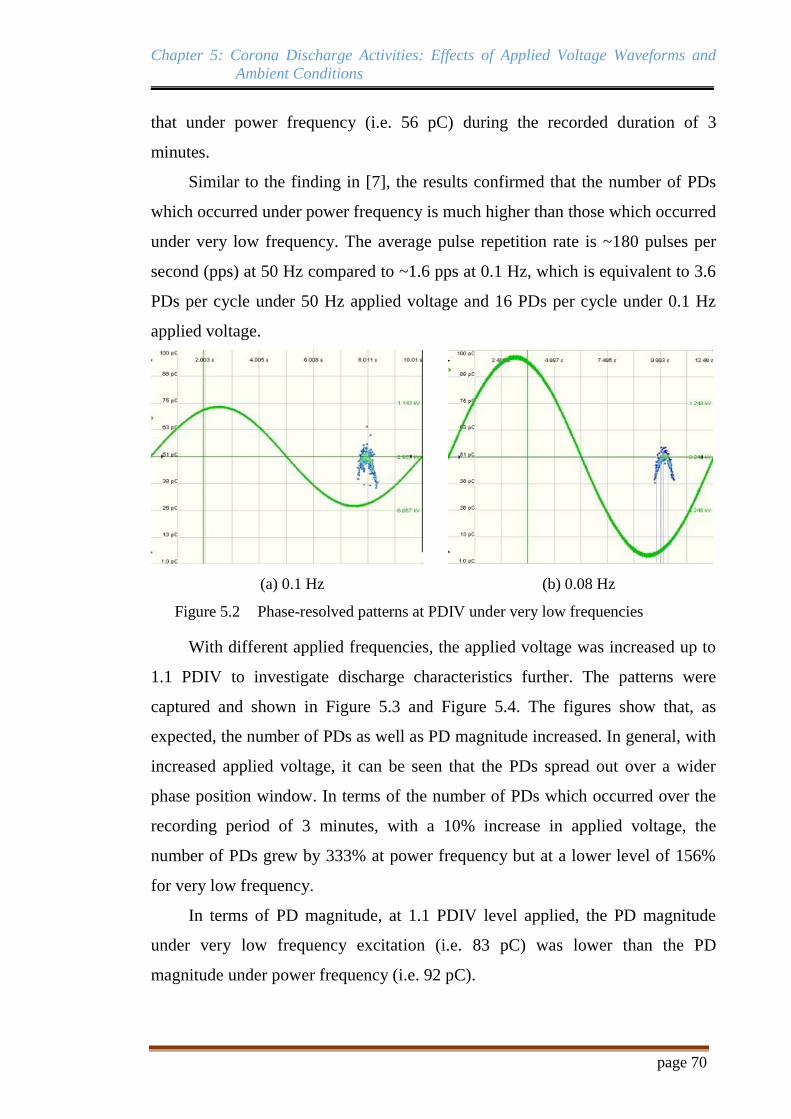
Chapter 5: Corona Discharge Activities: Effects of Applied Voltage Waveforms and
Ambient Conditions
page 70
that under power frequency (i.e. 56 pC) during the recorded duration of 3
minutes.
Similar to the finding in [7], the results confirmed that the number of PDs
which occurred under power frequency is much higher than those which occurred
under very low frequency. The average pulse repetition rate is ~180 pulses per
second (pps) at 50 Hz compared to ~1.6 pps at 0.1 Hz, which is equivalent to 3.6
PDs per cycle under 50 Hz applied voltage and 16 PDs per cycle under 0.1 Hz
applied voltage.
(a) 0.1 Hz (b) 0.08 Hz
Figure 5.2 Phase-resolved patterns at PDIV under very low frequencies
With different applied frequencies, the applied voltage was increased up to
1.1 PDIV to investigate discharge characteristics further. The patterns were
captured and shown in Figure 5.3 and Figure 5.4. The figures show that, as
expected, the number of PDs as well as PD magnitude increased. In general, with
increased applied voltage, it can be seen that the PDs spread out over a wider
phase position window. In terms of the number of PDs which occurred over the
recording period of 3 minutes, with a 10% increase in applied voltage, the
number of PDs grew by 333% at power frequency but at a lower level of 156%
for very low frequency.
In terms of PD magnitude, at 1.1 PDIV level applied, the PD magnitude
under very low frequency excitation (i.e. 83 pC) was lower than the PD
magnitude under power frequency (i.e. 92 pC).
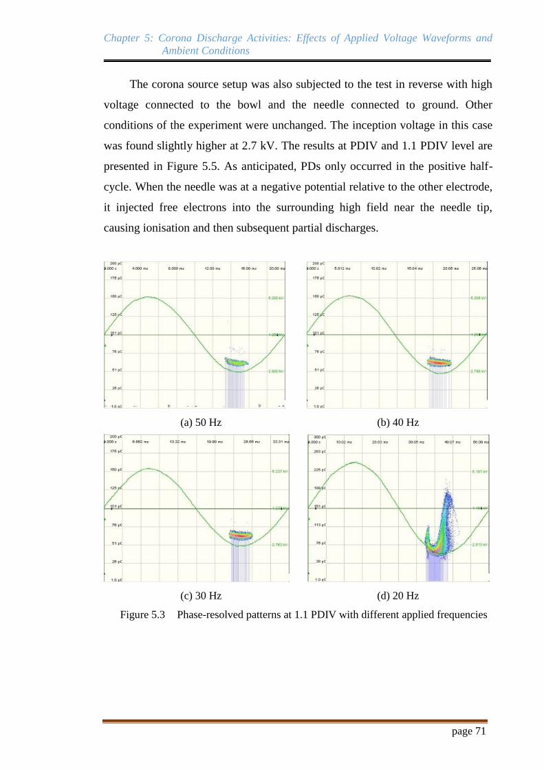
Chapter 5: Corona Discharge Activities: Effects of Applied Voltage Waveforms and
Ambient Conditions
page 71
The corona source setup was also subjected to the test in reverse with high
voltage connected to the bowl and the needle connected to ground. Other
conditions of the experiment were unchanged. The inception voltage in this case
was found slightly higher at 2.7 kV. The results at PDIV and 1.1 PDIV level are
presented in Figure 5.5. As anticipated, PDs only occurred in the positive half-
cycle. When the needle was at a negative potential relative to the other electrode,
it injected free electrons into the surrounding high field near the needle tip,
causing ionisation and then subsequent partial discharges.
(a) 50 Hz (b) 40 Hz
(c) 30 Hz (d) 20 Hz
Figure 5.3 Phase-resolved patterns at 1.1 PDIV with different applied frequencies

Chapter 5: Corona Discharge Activities: Effects of Applied Voltage Waveforms and
Ambient Conditions
page 72
(a) 0.1 Hz (b) 0.08 Hz
Figure 5.4 Phase-resolved patterns at 1.1 PDIV with different applied frequencies
(a) PDIV (b) 1.1 PDIV
Figure 5.5 Reverse testing at 0.1 Hz at different voltage levels
5.2.2 Corona discharge at very low frequency under excitation of square
waveform
In this section, the needle and bowl test object was subjected to square
voltage at the excited frequency of 0.1 Hz. The voltage level was increased
gradually in steps of 100 V to determine the inception value of corona discharge.
The PDIV was found at 3.8 kV. Phase-resolved PD patterns at PDIV and 1.05
PDIV level are shown in Figure 5.6 and PD characteristics are summarised in
Table 5.1. Figure 5.6 shows that PD activities only occurred in the negative half-
cycle at both voltage levels. Unlike the distribution of PD events in the case of
sine wave, corona discharges spread out almost over the whole half-cycle under
square voltage. This dissimilarity could be caused by the duration of voltage peak
magnitude on electrodes. In the square waveform case, the voltage at the needle
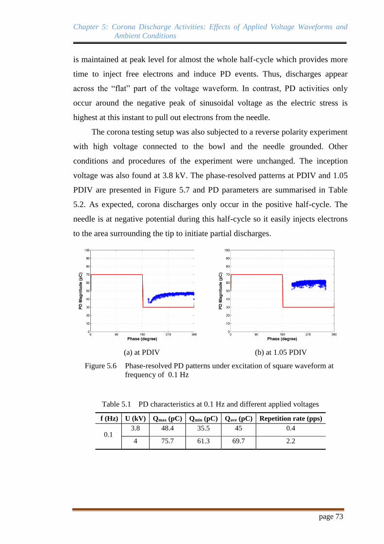
Chapter 5: Corona Discharge Activities: Effects of Applied Voltage Waveforms and
Ambient Conditions
page 73
is maintained at peak level for almost the whole half-cycle which provides more
time to inject free electrons and induce PD events. Thus, discharges appear
across the “flat” part of the voltage waveform. In contrast, PD activities only
occur around the negative peak of sinusoidal voltage as the electric stress is
highest at this instant to pull out electrons from the needle.
The corona testing setup was also subjected to a reverse polarity experiment
with high voltage connected to the bowl and the needle grounded. Other
conditions and procedures of the experiment were unchanged. The inception
voltage was also found at 3.8 kV. The phase-resolved patterns at PDIV and 1.05
PDIV are presented in Figure 5.7 and PD parameters are summarised in Table
5.2. As expected, corona discharges only occur in the positive half-cycle. The
needle is at negative potential during this half-cycle so it easily injects electrons
to the area surrounding the tip to initiate partial discharges.
(a) at PDIV (b) at 1.05 PDIV
Figure 5.6 Phase-resolved PD patterns under excitation of square waveform at
frequency of 0.1 Hz
Table 5.1 PD characteristics at 0.1 Hz and different applied voltages
f (Hz) U (kV) Qmax (pC) Qmin (pC) Qave (pC) Repetition rate (pps)
0.1 3.8 48.4 35.5 45 0.4
4 75.7 61.3 69.7 2.2
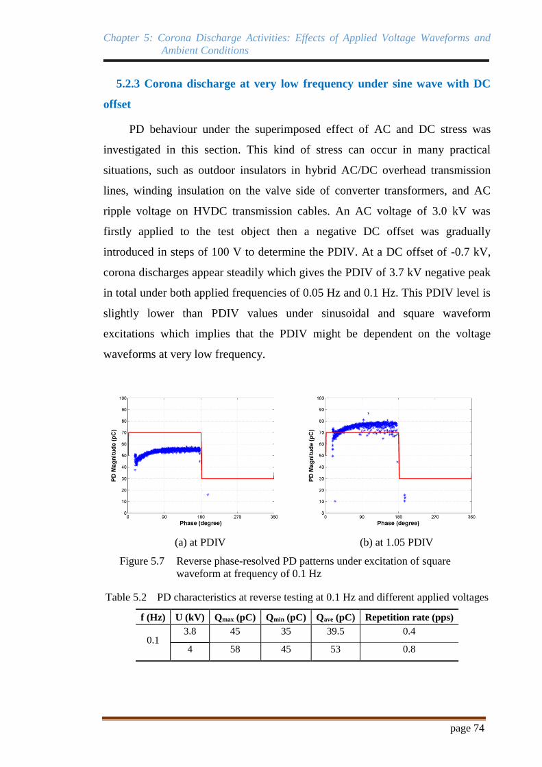
Chapter 5: Corona Discharge Activities: Effects of Applied Voltage Waveforms and
Ambient Conditions
page 74
5.2.3 Corona discharge at very low frequency under sine wave with DC
offset
PD behaviour under the superimposed effect of AC and DC stress was
investigated in this section. This kind of stress can occur in many practical
situations, such as outdoor insulators in hybrid AC/DC overhead transmission
lines, winding insulation on the valve side of converter transformers, and AC
ripple voltage on HVDC transmission cables. An AC voltage of 3.0 kV was
firstly applied to the test object then a negative DC offset was gradually
introduced in steps of 100 V to determine the PDIV. At a DC offset of -0.7 kV,
corona discharges appear steadily which gives the PDIV of 3.7 kV negative peak
in total under both applied frequencies of 0.05 Hz and 0.1 Hz. This PDIV level is
slightly lower than PDIV values under sinusoidal and square waveform
excitations which implies that the PDIV might be dependent on the voltage
waveforms at very low frequency.
(a) at PDIV (b) at 1.05 PDIV
Figure 5.7 Reverse phase-resolved PD patterns under excitation of square
waveform at frequency of 0.1 Hz
Table 5.2 PD characteristics at reverse testing at 0.1 Hz and different applied voltages
f (Hz) U (kV) Qmax (pC) Qmin (pC) Qave (pC) Repetition rate (pps)
0.1 3.8 45 35 39.5 0.4
4 58 45 53 0.8

Chapter 5: Corona Discharge Activities: Effects of Applied Voltage Waveforms and
Ambient Conditions
page 75
In terms of PD characteristics, phase-resolved PD patterns are shown in
Figure 5.8 and PD parameters are summarised in Table 5.3. Average PD position
is around the negative peak at 270 as expected for corona discharges. However,
the repetition rate of PD events of 26.9 pps at 0.1 Hz is larger than that of 3.45
pps at 0.05 Hz. PD magnitude at 0.1 Hz is also scattered over a slightly wider
range of 21 pC to 227 pC than the range under 0.05 Hz of 28 pC to 205 pC.
These differences might be due to the voltage rise rate at the negative half-cycle
as in the case of the square voltage wave presented above. The higher rate of rise
might result in higher PD magnitudes and repetition rate.
(a) at 0.05 Hz (b) at 0.1 Hz
Figure 5.8 Phase-resolved PD patterns at PDIV with DC offset of -0.7 kV at
different applied frequencies
The DC offset was then extended to -0.8 kV to investigate its effect on the
PD behaviours. Phase-resolved PD patterns and characteristics are shown in
Figure 5.9 and Table 5.4. At the negative applied voltage peak of -3.8 kV, it can
be observed that PD positions have changed considerably. The discharges occur
earlier than the previous case under applied frequency of 0.1 Hz. Average phase
angle of the distribution shifts from 270 to 254 when the DC offset value is
reduced. On the other hand, this value only changes slightly from 269 to 265
under the applied frequency of 0.05 Hz which suggests that at higher AC-DC
applied voltage, PD activities tend to occur earlier in the voltage cycle.
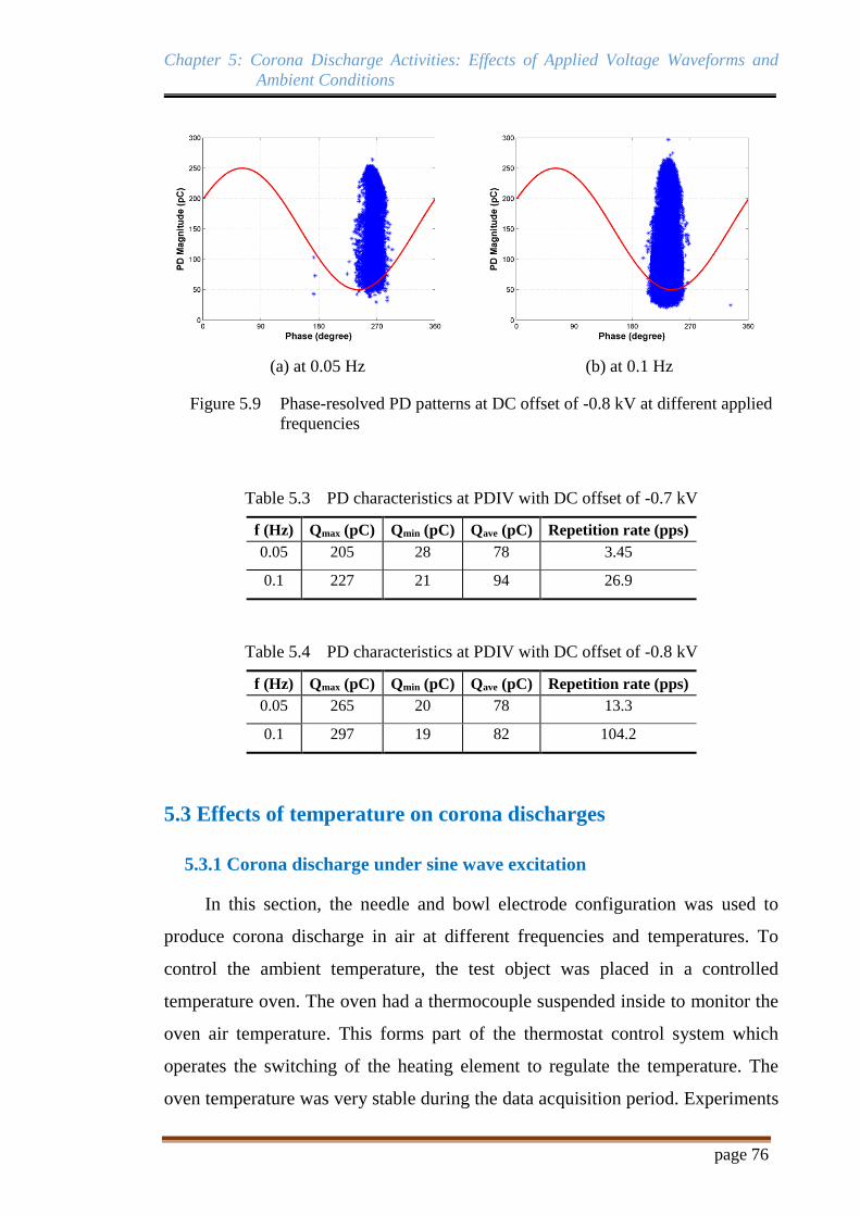
Chapter 5: Corona Discharge Activities: Effects of Applied Voltage Waveforms and
Ambient Conditions
page 76
(a) at 0.05 Hz (b) at 0.1 Hz
Figure 5.9 Phase-resolved PD patterns at DC offset of -0.8 kV at different applied
frequencies
Table 5.3 PD characteristics at PDIV with DC offset of -0.7 kV
f (Hz) Qmax (pC) Qmin (pC) Qave (pC) Repetition rate (pps)
0.05 205 28 78 3.45
0.1 227 21 94 26.9
Table 5.4 PD characteristics at PDIV with DC offset of -0.8 kV
f (Hz) Qmax (pC) Qmin (pC) Qave (pC) Repetition rate (pps)
0.05 265 20 78 13.3
0.1 297 19 82 104.2
5.3 Effects of temperature on corona discharges
5.3.1 Corona discharge under sine wave excitation
In this section, the needle and bowl electrode configuration was used to
produce corona discharge in air at different frequencies and temperatures. To
control the ambient temperature, the test object was placed in a controlled
temperature oven. The oven had a thermocouple suspended inside to monitor the
oven air temperature. This forms part of the thermostat control system which
operates the switching of the heating element to regulate the temperature. The
oven temperature was very stable during the data acquisition period. Experiments

Chapter 5: Corona Discharge Activities: Effects of Applied Voltage Waveforms and
Ambient Conditions
page 77
were conducted at four different temperatures as read from the optical-fibre
thermometer: 20C, 30C, 35C and 40C. Because of the temperature constraint
due to the perspex material used to make the housing of the test object, it was not
possible to conduct the experiment at temperatures exceeding 45C.
By using the function generator, the applied frequency was varied from
power frequency (50 Hz) to very low frequency (0.1 Hz). Phase-resolved partial
discharge activities are recorded under each applied frequency at room
temperature (20C) and above (30C, 35C and 40C). The partial discharge
inception voltage (PDIV) was determined by gradually increasing in steps of 100
V until steady PDs were observed. PD magnitudes were recorded for those pulses
above the threshold of 10 pC to eliminate background noise in the test facility.
Due to PD stochastic characteristics, the recorded time must be set long enough
to achieve a stable PD trend at each applied frequency. In this work, this is equal
to 90 full voltage cycles for the very low frequency range (0.1 Hz and 0.05 Hz).
Figure 5.10 shows the phase-resolved PD patterns of corona discharges at
0.1 Hz at four different temperatures (20C, 30C, 35C and 40C) at PDIV.
Results are consistent at each temperature level when the experiments were
repeated five times. The PDIV of 3.9 kV peak is found for all four cases. As can
be observed from Figure 5.10, PD activities occur in the negative half-cycle. The
highest stress applied is only 1.1 PDIV so no PDs in the positive half-cycle are
anticipated from the test object. The presence of a few disturbances observed in
some of the results is believed to be from external interference.
(a) 20C (b) 30C
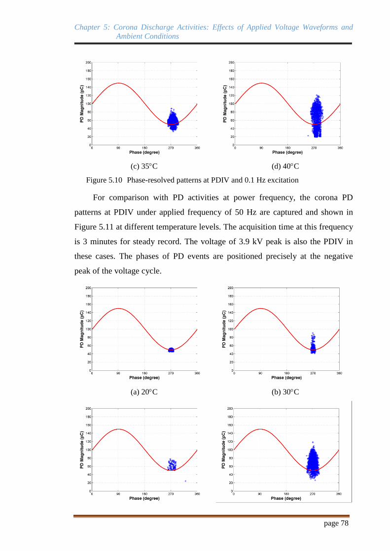
Chapter 5: Corona Discharge Activities: Effects of Applied Voltage Waveforms and
Ambient Conditions
page 78
(c) 35C (d) 40C
Figure 5.10 Phase-resolved patterns at PDIV and 0.1 Hz excitation
For comparison with PD activities at power frequency, the corona PD
patterns at PDIV under applied frequency of 50 Hz are captured and shown in
Figure 5.11 at different temperature levels. The acquisition time at this frequency
is 3 minutes for steady record. The voltage of 3.9 kV peak is also the PDIV in
these cases. The phases of PD events are positioned precisely at the negative
peak of the voltage cycle.
(a) 20C (b) 30C
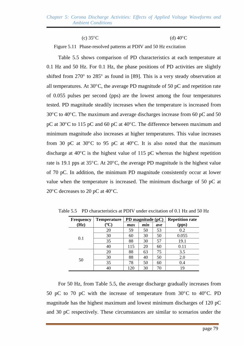
Chapter 5: Corona Discharge Activities: Effects of Applied Voltage Waveforms and
Ambient Conditions
page 79
(c) 35C (d) 40C
Figure 5.11 Phase-resolved patterns at PDIV and 50 Hz excitation
Table 5.5 shows comparison of PD characteristics at each temperature at
0.1 Hz and 50 Hz. For 0.1 Hz, the phase positions of PD activities are slightly
shifted from 270 to 285 as found in [89]. This is a very steady observation at
all temperatures. At 30C, the average PD magnitude of 50 pC and repetition rate
of 0.055 pulses per second (pps) are the lowest among the four temperatures
tested. PD magnitude steadily increases when the temperature is increased from
30C to 40C. The maximum and average discharges increase from 60 pC and 50
pC at 30C to 115 pC and 60 pC at 40C. The difference between maximum and
minimum magnitude also increases at higher temperatures. This value increases
from 30 pC at 30C to 95 pC at 40C. It is also noted that the maximum
discharge at 40C is the highest value of 115 pC whereas the highest repetition
rate is 19.1 pps at 35C. At 20C, the average PD magnitude is the highest value
of 70 pC. In addition, the minimum PD magnitude consistently occur at lower
value when the temperature is increased. The minimum discharge of 50 pC at
20C decreases to 20 pC at 40C.
Table 5.5 PD characteristics at PDIV under excitation of 0.1 Hz and 50 Hz
Frequency
(Hz)
Temperature
(oC)
PD magnitude (pC) Repetition rate
(pps) max min ave
0.1
20 59 50 53 0.2
30 60 30 50 0.055
35 88 30 57 19.1
40 115 20 60 0.11
50
20 88 63 75 3.5
30 88 40 50 2.0
35 78 50 60 0.4
40 120 30 70 19
For 50 Hz, from Table 5.5, the average discharge gradually increases from
50 pC to 70 pC with the increase of temperature from 30C to 40C. PD
magnitude has the highest maximum and lowest minimum discharges of 120 pC
and 30 pC respectively. These circumstances are similar to scenarios under the
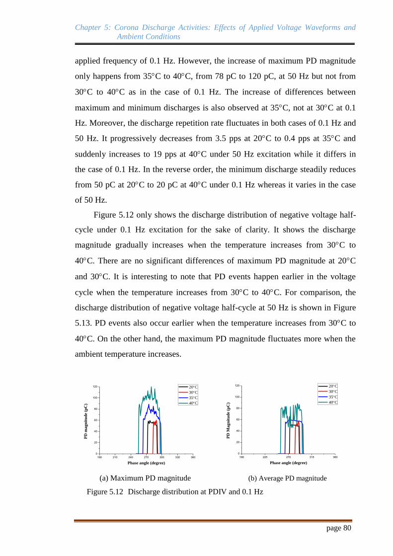
Chapter 5: Corona Discharge Activities: Effects of Applied Voltage Waveforms and
Ambient Conditions
page 80
applied frequency of 0.1 Hz. However, the increase of maximum PD magnitude
only happens from 35C to 40C, from 78 pC to 120 pC, at 50 Hz but not from
30C to 40C as in the case of 0.1 Hz. The increase of differences between
maximum and minimum discharges is also observed at 35C, not at 30C at 0.1
Hz. Moreover, the discharge repetition rate fluctuates in both cases of 0.1 Hz and
50 Hz. It progressively decreases from 3.5 pps at 20C to 0.4 pps at 35C and
suddenly increases to 19 pps at 40C under 50 Hz excitation while it differs in
the case of 0.1 Hz. In the reverse order, the minimum discharge steadily reduces
from 50 pC at 20C to 20 pC at 40C under 0.1 Hz whereas it varies in the case
of 50 Hz.
Figure 5.12 only shows the discharge distribution of negative voltage half-
cycle under 0.1 Hz excitation for the sake of clarity. It shows the discharge
magnitude gradually increases when the temperature increases from 30C to
40C. There are no significant differences of maximum PD magnitude at 20C
and 30C. It is interesting to note that PD events happen earlier in the voltage
cycle when the temperature increases from 30C to 40C. For comparison, the
discharge distribution of negative voltage half-cycle at 50 Hz is shown in Figure
5.13. PD events also occur earlier when the temperature increases from 30C to
40C. On the other hand, the maximum PD magnitude fluctuates more when the
ambient temperature increases.
180 210 240 270 300 330 360
0
20
40
60
80
100
120 20C
30C
35C
40C
PD
ma
gn
itu
de
(pC
)
Phase angle (degree)
180 225 270 315 360
0
20
40
60
80
100
120 20C
30C
35C
40C
PD
Ma
gn
itu
de
(pC
)
Phase angle (degree)
(a) Maximum PD magnitude (b) Average PD magnitude
Figure 5.12 Discharge distribution at PDIV and 0.1 Hz

Chapter 5: Corona Discharge Activities: Effects of Applied Voltage Waveforms and
Ambient Conditions
page 81
180 210 240 270 300 330 360
0
20
40
60
80
100
120 20C
30C
35C
40CP
D m
ag
nit
ud
e (p
C)
Phase angle (degree)
180 225 270 315 360
0
20
40
60
80
100
120 20C
30C
35C
40C
PD
ma
gn
itu
de
(pC
)
Phase angle (degree)
(a) Maximum PD magnitude (b) Average PD magnitude
Figure 5.13 Discharge distribution at PDIV and 50 Hz
To investigate PD activities at higher voltage stress, the voltage level of 1.1
PDIV is applied under both 0.1 Hz and 50 Hz excitation at different
temperatures. Figure 5.14 and Figure 5.15 show the patterns of corona discharges
at different temperatures under 0.1 Hz and 50 Hz excitation, respectively, when
1.1 PDIV is applied to investigate PD activities at above PDIV. The PD
characteristics are summarised in Table 5.6. It can be seen from Table 5.6 that
previous findings at PDIV are also observed at this voltage level. The average
discharges gradually increase when the ambient temperature increases, from 66
pC at 30C to 98 pC at 40C in the case of 0.1 Hz and from 54 pC at 20C to 68
pC at 40C at power frequency. At 40C, the maximum PD magnitude which is
approximately 200 pC at both applied frequencies of 0.1 Hz and 50 Hz is the
highest value. The minimum discharge at this temperature is also the lowest at
both frequencies.
Table 5.6 PD characteristics at 1.1 PDIV under excitation of 0.1 Hz and 50 Hz
Frequency
(Hz)
Temperature
(oC)
PD magnitude (pC) Repetition rate
(pps) max min ave
0.1
20 98 32 55 1108
30 116 23 66 465
35 100 35 63 1155
40 200 30 98 45
50
20 77 30 54 1215
30 120 25 57 6
35 85 34 60 1195
40 197 20 68 79
However, similar trends of PD phase distribution to PDIV patterns are only
obtained under power frequency excitation while the PD characteristics for 0.1
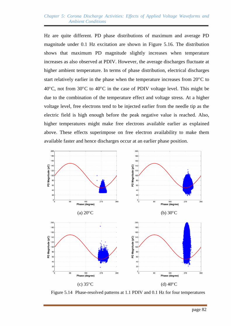
Chapter 5: Corona Discharge Activities: Effects of Applied Voltage Waveforms and
Ambient Conditions
page 82
Hz are quite different. PD phase distributions of maximum and average PD
magnitude under 0.1 Hz excitation are shown in Figure 5.16. The distribution
shows that maximum PD magnitude slightly increases when temperature
increases as also observed at PDIV. However, the average discharges fluctuate at
higher ambient temperature. In terms of phase distribution, electrical discharges
start relatively earlier in the phase when the temperature increases from 20C to
40C, not from 30C to 40C in the case of PDIV voltage level. This might be
due to the combination of the temperature effect and voltage stress. At a higher
voltage level, free electrons tend to be injected earlier from the needle tip as the
electric field is high enough before the peak negative value is reached. Also,
higher temperatures might make free electrons available earlier as explained
above. These effects superimpose on free electron availability to make them
available faster and hence discharges occur at an earlier phase position.
(a) 20C (b) 30C
(c) 35C (d) 40C
Figure 5.14 Phase-resolved patterns at 1.1 PDIV and 0.1 Hz for four temperatures
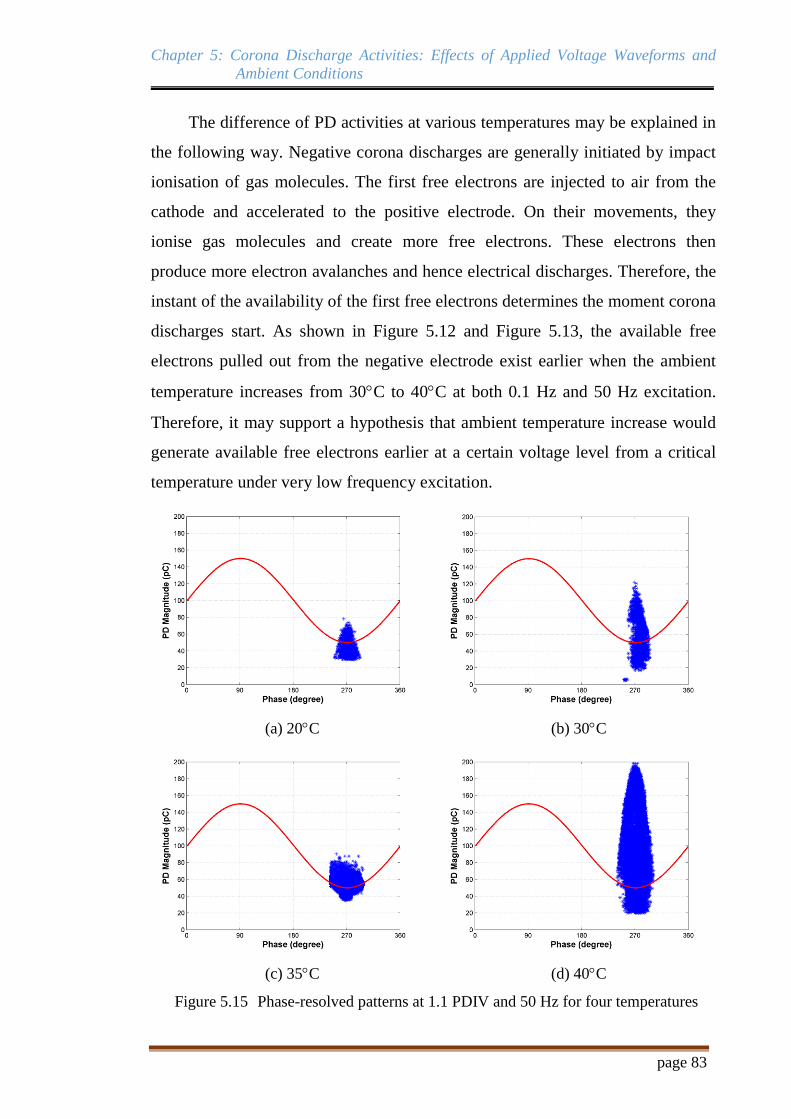
Chapter 5: Corona Discharge Activities: Effects of Applied Voltage Waveforms and
Ambient Conditions
page 83
The difference of PD activities at various temperatures may be explained in
the following way. Negative corona discharges are generally initiated by impact
ionisation of gas molecules. The first free electrons are injected to air from the
cathode and accelerated to the positive electrode. On their movements, they
ionise gas molecules and create more free electrons. These electrons then
produce more electron avalanches and hence electrical discharges. Therefore, the
instant of the availability of the first free electrons determines the moment corona
discharges start. As shown in Figure 5.12 and Figure 5.13, the available free
electrons pulled out from the negative electrode exist earlier when the ambient
temperature increases from 30C to 40C at both 0.1 Hz and 50 Hz excitation.
Therefore, it may support a hypothesis that ambient temperature increase would
generate available free electrons earlier at a certain voltage level from a critical
temperature under very low frequency excitation.
(a) 20C (b) 30C
(c) 35C (d) 40C
Figure 5.15 Phase-resolved patterns at 1.1 PDIV and 50 Hz for four temperatures
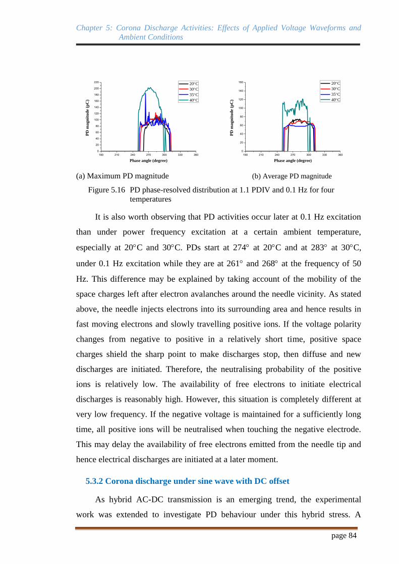
Chapter 5: Corona Discharge Activities: Effects of Applied Voltage Waveforms and
Ambient Conditions
page 84
180 210 240 270 300 330 360
0
20
40
60
80
100
120
140
160
180
200
220 20C
30C
35C
40C
PD
ma
gn
itu
de
(pC
)
Phase angle (degree)
180 210 240 270 300 330 360
0
20
40
60
80
100
120
140
160 20C
30C
35C
40C
PD
ma
gn
itu
de
(pC
)
Phase angle (degree)
(a) Maximum PD magnitude (b) Average PD magnitude
Figure 5.16 PD phase-resolved distribution at 1.1 PDIV and 0.1 Hz for four
temperatures
It is also worth observing that PD activities occur later at 0.1 Hz excitation
than under power frequency excitation at a certain ambient temperature,
especially at 20C and 30C. PDs start at 274 at 20C and at 283 at 30C,
under 0.1 Hz excitation while they are at 261 and 268 at the frequency of 50
Hz. This difference may be explained by taking account of the mobility of the
space charges left after electron avalanches around the needle vicinity. As stated
above, the needle injects electrons into its surrounding area and hence results in
fast moving electrons and slowly travelling positive ions. If the voltage polarity
changes from negative to positive in a relatively short time, positive space
charges shield the sharp point to make discharges stop, then diffuse and new
discharges are initiated. Therefore, the neutralising probability of the positive
ions is relatively low. The availability of free electrons to initiate electrical
discharges is reasonably high. However, this situation is completely different at
very low frequency. If the negative voltage is maintained for a sufficiently long
time, all positive ions will be neutralised when touching the negative electrode.
This may delay the availability of free electrons emitted from the needle tip and
hence electrical discharges are initiated at a later moment.
5.3.2 Corona discharge under sine wave with DC offset
As hybrid AC-DC transmission is an emerging trend, the experimental
work was extended to investigate PD behaviour under this hybrid stress. A
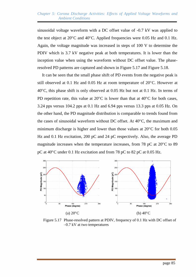
Chapter 5: Corona Discharge Activities: Effects of Applied Voltage Waveforms and
Ambient Conditions
page 85
sinusoidal voltage waveform with a DC offset value of -0.7 kV was applied to
the test object at 20C and 40C. Applied frequencies were 0.05 Hz and 0.1 Hz.
Again, the voltage magnitude was increased in steps of 100 V to determine the
PDIV which is 3.7 kV negative peak at both temperatures. It is lower than the
inception value when using the waveform without DC offset value. The phase-
resolved PD patterns are captured and shown in Figure 5.17 and Figure 5.18.
It can be seen that the small phase shift of PD events from the negative peak is
still observed at 0.1 Hz and 0.05 Hz at room temperature of 20C. However at
40C, this phase shift is only observed at 0.05 Hz but not at 0.1 Hz. In terms of
PD repetition rate, this value at 20C is lower than that at 40C for both cases,
3.24 pps versus 104.2 pps at 0.1 Hz and 6.94 pps versus 13.3 pps at 0.05 Hz. On
the other hand, the PD magnitude distribution is comparable to trends found from
the cases of sinusoidal waveform without DC offset. At 40C, the maximum and
minimum discharge is higher and lower than those values at 20C for both 0.05
Hz and 0.1 Hz excitation, 200 pC and 24 pC respectively. Also, the average PD
magnitude increases when the temperature increases, from 78 pC at 20C to 89
pC at 40C under 0.1 Hz excitation and from 78 pC to 82 pC at 0.05 Hz.
(a) 20C (b) 40C
Figure 5.17 Phase-resolved pattern at PDIV, frequency of 0.1 Hz with DC offset of
–0.7 kV at two temperatures

Chapter 5: Corona Discharge Activities: Effects of Applied Voltage Waveforms and
Ambient Conditions
page 86
(a) 20C (b) 40C
Figure 5.18 Phase-resolved pattern at PDIV, frequency of 0.05Hz with DC offset of
–0.7 kV at two different temperatures
5.4 Conclusion
This chapter reported a comprehensive study of corona discharges at
different applied voltage waveforms (sinusoidal wave and square wave) under
the excitation of very low frequency, i.e. 0.1 Hz. Experimental results show that
the inception voltage of corona discharges at very low frequency is dependent on
applied voltage waveforms. Under the application of a square wave and sine
wave with DC offset, corona discharges are initiated at lower voltage amplitude
than under a pure sinusoidal waveform. This could be mainly due to the longer
duration of the high level of negative voltage amplitude to trigger negative
corona discharges. There is also evidence to suggest that the rate of voltage rise
affects discharge characteristics. A faster rate of voltage rise causes more
discharges and larger magnitudes.
The effects of ambient air on corona discharges were investigated
thoroughly at four temperature points between 20C and 40C at very low
frequency excitation and power frequency for the sake of comparison. Measured
corona discharge characteristics show that the increase of ambient temperature
results in larger discharge magnitude and causes corona discharges to occur
earlier in the phase of the voltage cycle. This might be due to more availability of
free electrons emitted from the negative electrode at higher temperatures. The
following chapter extends the partial discharge investigation at very low

Chapter 5: Corona Discharge Activities: Effects of Applied Voltage Waveforms and
Ambient Conditions
page 87
frequency by performing partial discharge measurements in a cavity as a function
of cavity size and applied voltage waveforms.

page 88
Chapter 6: Void Discharge
Behaviours as a Function of Cavity
Size and Applied Waveforms
6.1 Introduction
This chapter reports measured PD characteristics in a cylindrical void
embedded in the insulation material under the excitation of very low frequency
and power frequency. The test samples were described in Chapter 4. In this
investigation, various voltage waveforms such as sinusoidal wave, trapezoidal
wave and user-customised wave were applied to stress the test objects under
different conditions to investigate PD behaviours. PD characteristics obtained at
very low frequency and power frequency are discussed thoroughly to study
effects of cavity size and applied waveforms at both frequencies.
Section 6.2 presents the trend of partial discharge activities occurring
continuously over a long period of time at 0.1 Hz and 50 Hz. Section 6.3 reports
the partial discharge characteristics in different cavity sizes under very low
frequency and power frequency excitation. The effects of voltage waveforms on
internal discharge are presented in Section 6.4.
6.2 Discharge behaviours under long exposure to partial discharge
6.2.1 Partial discharge characteristics under excitation of sine wave
This section describes how PD characteristics change over the test duration
at two different frequencies, 0.1 Hz and 50 Hz, under excitation of sine wave
voltage. PD activities in the insulated void are measured at applied voltage
amplitude of 10 kV. Experiments were performed for a duration of 4 hours, using
a new test object at each frequency. PD measurements were recorded periodically

Chapter 6: Void Discharge Behaviours as a Function of Cavity Size and Applied
Waveforms
page 89
every hour from the beginning of the voltage application at each applied
frequency. PD characteristics were measured for a duration of 15 minutes at the
0.1 Hz frequency (i.e. 90 full voltage AC cycles), and for 5 minutes at the 50 Hz
frequency. As expected, PD patterns are mostly symmetrical in positive and
negative half-cycles at both 0.1 Hz and 50 Hz. Hence, PD data are only shown
here in the positive half-cycle for comparison.
Figure 6.1 shows the maximum and average PD magnitude at different
points in time during the testing period at 0.1 Hz and 50 Hz. At the beginning of
the testing period, large discharges occur as shown in Figure 6.1. After 1 hour of
applied voltage, PD characteristics at both frequencies change significantly. For
the case of 50 Hz, the maximum PD magnitude reduces greatly to 1628 pC as
compared to 2548 pC at the start. A similar decrease is also observed at 0.1 Hz,
from 3192 pC to 2510 pC. In terms of average magnitude, the decrease of PD
magnitude is only seen at 50 Hz, from 1771 pC to 862 pC, whereas this value
does not change much at 0.1 Hz.
Figure 6.1 Maximum and average PD magnitude at 0.1 Hz and 50 Hz
From 1 hour after the test start, there are clearly different trends of PD
magnitudes at 0.1 Hz and 50 Hz. Under applied frequency of 50 Hz, both
maximum and average PD magnitude gradually increase to 2282 pC and 1501
pC respectively until 3 hours after the start and then suddenly decrease to 2100
0
500
1000
1500
2000
2500
3000
3500
0 1 2 3 4
PD
mag
nit
ud
e (p
C)
Time (h)
0.1 Hz Q_average
0.1 Hz Q_max
50 Hz Q_average
50 Hz Q_max

Chapter 6: Void Discharge Behaviours as a Function of Cavity Size and Applied
Waveforms
page 90
pC and 943 pC. On the other hand, for 0.1 Hz, maximum PD magnitude
continues decreasing over time while average PD value slightly fluctuates. Figure
6.2 shows only the phase-resolved PD patterns for 0.1 Hz and 50 Hz at 1 hour
and 4 hours after applying voltages as they reveal great difference in PD
activities.
(a) 0.1 Hz at 1 hour (b) 0.1 Hz at 4 hours
(c) 50 Hz at 1 hour (d) 50 Hz at 4 hours
Figure 6.2 Phase-resolved PD patterns at 0.1 Hz (a, b) and 50 Hz (c, d) at 1 and 4
hours after applying voltages
Regarding the phase position of PD activity, discharges are generally
observed later in the phase at frequency of 0.1 Hz when compared with higher
applied frequency, similar to [90] and [91], as shown in Figure 6.3. It is
interesting to note that PD activity happens at higher instantaneous voltage value
at the beginning for both frequencies, and then it occurs earlier in the voltage
cycle after applying voltage for a while. At 50 Hz excitation, PD activities occur
steadily from 1 hour after applying voltage, with average phase distribution of
45. However, this is not the case at 0.1 Hz. The average phase distribution of

Chapter 6: Void Discharge Behaviours as a Function of Cavity Size and Applied
Waveforms
page 91
discharges gradually decreases from the start till 3 hours later, from 93.7 to
73.6, and then increases to 84.1 when the testing period ends. It means that PD
activity steadily occurs earlier when the voltage is applied longer to a certain
point of time, then it happens slightly later in the phase.
In general, PD activities over long duration of applied sine voltage could be
characterised in two stages at both frequencies. In the first stage, large electric
discharges occur at the beginning and the discharge magnitude rapidly decreases.
This could be due to a statistical time lag. At the beginning of testing, lack of
initial free electrons for igniting discharges inside the cavity may cause
discharges to occur at higher voltage across the cavity; therefore magnitudes of
PD activities are large. The second stage begins with smaller discharges when
more free electrons are generated from the cavity surface and previous
discharges. However, durations of these two degradation stages are different at
0.1 Hz and 50 Hz. It takes less than 1 hour to finish the first stage at 50 Hz but
more than 3 hours at 0.1 Hz. This time discrepancy is likely to be explained by
changes of physical parameters such as surface conductivity of the cavity and
charge decay mechanisms.
Figure 6.3 Average phase distribution at 0.1 Hz and 50 Hz
When PDs occur inside the cavity, byproducts produced during discharges
are deposited on the cavity surface; hence, surface conductivity of the cavity is
changed [46]. Surface conductivity of the cavity and bulk conductivity of the
insulation material surrounding the cavity are also at their lowest value when
0
10
20
30
40
50
60
70
80
90
100
0 1 2 3 4
Ph
ase
An
gle
(deg
ree)
Time (h)
0.1 Hz
50 Hz

Chapter 6: Void Discharge Behaviours as a Function of Cavity Size and Applied
Waveforms
page 92
PDs happen. Charges and byproducts generated from discharges cover the
surface of the cavity and they act as a shield to slightly decrease the electric field
across the cavity. As a result, maximum PD magnitude decreases. This process
takes longer at 0.1 Hz than at 50 Hz so it takes more time to finish the first stage
at 0.1 Hz than at 50 Hz.
Charge decay mechanisms may also contribute to this time difference.
Charges spread over the area where PD activity happens. These charges can
decay via three possible mechanisms: surface conduction, bulk conduction and
neutralisation by recombination. As noted above, when PDs continue to occur
repeatedly, surface and bulk conductivity increases which accelerates the rate of
charge decay. Also, the rate of charge recombination is different under different
rates of voltage rise. The rate of charge decay is relatively less at higher
frequency. These reasons are likely to explain why PDs are observed later in the
voltage phase position and at higher voltage value at 0.1 Hz than at 50 Hz.
In terms of PD repetition rate, a trend found in [92] is also observed here at
50 Hz as shown in Figure 6.4. The number of PD events per second increases
during the first stage and then slowly decreases in the second stage. This increase
of PD repetition rate could be related to changes of gas composition and pressure
inside the cavity. According to [93], the amount of oxygen drops to very low
values due to PD activities. Hence, the lower the amount of oxygen, the higher
the probability of discharge occurrence as oxygen is an electro-negative gas. It is
also shown in [94] that the gas pressure inside the cavity may decrease when
discharges start to ignite. As the pressure in this study is at normal conditions, i.e
1 atm of atmospheric pressure, and cavity dimensions are small, a drop in
pressure would reduce the breakdown strength according to Paschen’s law which
could explain the increase in PD repetition rate. At the second stage, the
reduction of electric field in the cavity due to the accumulation of PD byproducts
and charges might decrease the number of PDs.
On the other hand, it is worth noting that the PD repetition rate under 0.1
Hz excitation gradually decreases in the first aging stage and slightly increases in
the second aging stage. At the first stage, the charge decay rate is relatively high
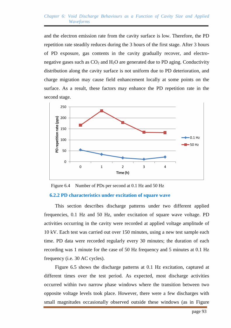
Chapter 6: Void Discharge Behaviours as a Function of Cavity Size and Applied
Waveforms
page 93
and the electron emission rate from the cavity surface is low. Therefore, the PD
repetition rate steadily reduces during the 3 hours of the first stage. After 3 hours
of PD exposure, gas contents in the cavity gradually recover, and electro-
negative gases such as CO2 and H2O are generated due to PD aging. Conductivity
distribution along the cavity surface is not uniform due to PD deterioration, and
charge migration may cause field enhancement locally at some points on the
surface. As a result, these factors may enhance the PD repetition rate in the
second stage.
Figure 6.4 Number of PDs per second at 0.1 Hz and 50 Hz
6.2.2 PD characteristics under excitation of square wave
This section describes discharge patterns under two different applied
frequencies, 0.1 Hz and 50 Hz, under excitation of square wave voltage. PD
activities occurring in the cavity were recorded at applied voltage amplitude of
10 kV. Each test was carried out over 150 minutes, using a new test sample each
time. PD data were recorded regularly every 30 minutes; the duration of each
recording was 1 minute for the case of 50 Hz frequency and 5 minutes at 0.1 Hz
frequency (i.e. 30 AC cycles).
Figure 6.5 shows the discharge patterns at 0.1 Hz excitation, captured at
different times over the test period. As expected, most discharge activities
occurred within two narrow phase windows where the transition between two
opposite voltage levels took place. However, there were a few discharges with
small magnitudes occasionally observed outside these windows (as in Figure
0
50
100
150
200
250
0 1 2 3 4
PD
re
pet
itio
n r
ate
(pp
s)
Time (h)
0.1 Hz
50 Hz

Chapter 6: Void Discharge Behaviours as a Function of Cavity Size and Applied
Waveforms
page 94
6.5a, 6.5c and 6.5f). The average discharge magnitude steadily increased during
the first 60 minutes of the voltage application and hardly changed from 90
minutes onward.
For comparison, the PD characteristics at 50 Hz frequency are shown in
Figure 6.6, similar to the PD patterns observed in another study [63]. Figure 6.7
shows the average PD magnitude at both 0.1 Hz and 50 Hz excitation. At the
beginning, discharges occurred with high magnitude (2000 pC) but decreased to
1076 pC after 30 minutes of voltage application. Then, the PD magnitude
increased gradually to 3129 pC at 60 minutes after applying voltage and to 5023
pC after 90 minutes. Fluctuation of discharge magnitude was observed after 2
hours of voltage application.
It is interesting to observe that discharge magnitudes are much larger at 50
Hz than at 0.1 Hz. This may be due to dependence of the PD magnitude on the
rate of rise of the applied voltage. Measurements showed that the high voltage
square waveform has a rise time of 112 s at 50 Hz and 12 ms at 0.1 Hz. The rise
time difference was due to limitations of the signal generator and high voltage
amplifier. In [95], surface charge accumulation was reported to be dependent on
the rise of voltage during the amplitude transition.
The charge polarisation process under square wave is illustrated in Figure
6.8. In this condition, a sudden polarity reversal replaces free charges of opposite
sign, and polarised charges represent the effect of dipoles. The dielectric is
polarised by the DC component of the square wave when the voltage is positive
(as in Figure 6.8a). Dipoles and free charges both exist at this period. When the
polarity reversal is happening, only dipoles which have higher relaxation
frequency could follow changes of the external electric field without any delay.
The remaining dipoles with lower relaxation frequency cannot respond quickly
during this time. Therefore, some charges would be bounded by these residual
dipoles when the voltage amplitude reaches zero value (Figure 6.8b). When the
voltage rapidly becomes negative (Figure 6.8c), opposite free charges promptly
accumulate on the surface and neutralise these bounded charges. However,
polarised charges due to lower relaxation frequency dipoles still remain and form
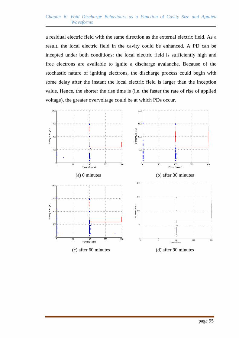
Chapter 6: Void Discharge Behaviours as a Function of Cavity Size and Applied
Waveforms
page 95
a residual electric field with the same direction as the external electric field. As a
result, the local electric field in the cavity could be enhanced. A PD can be
incepted under both conditions: the local electric field is sufficiently high and
free electrons are available to ignite a discharge avalanche. Because of the
stochastic nature of igniting electrons, the discharge process could begin with
some delay after the instant the local electric field is larger than the inception
value. Hence, the shorter the rise time is (i.e. the faster the rate of rise of applied
voltage), the greater overvoltage could be at which PDs occur.
(a) 0 minutes (b) after 30 minutes
(c) after 60 minutes (d) after 90 minutes
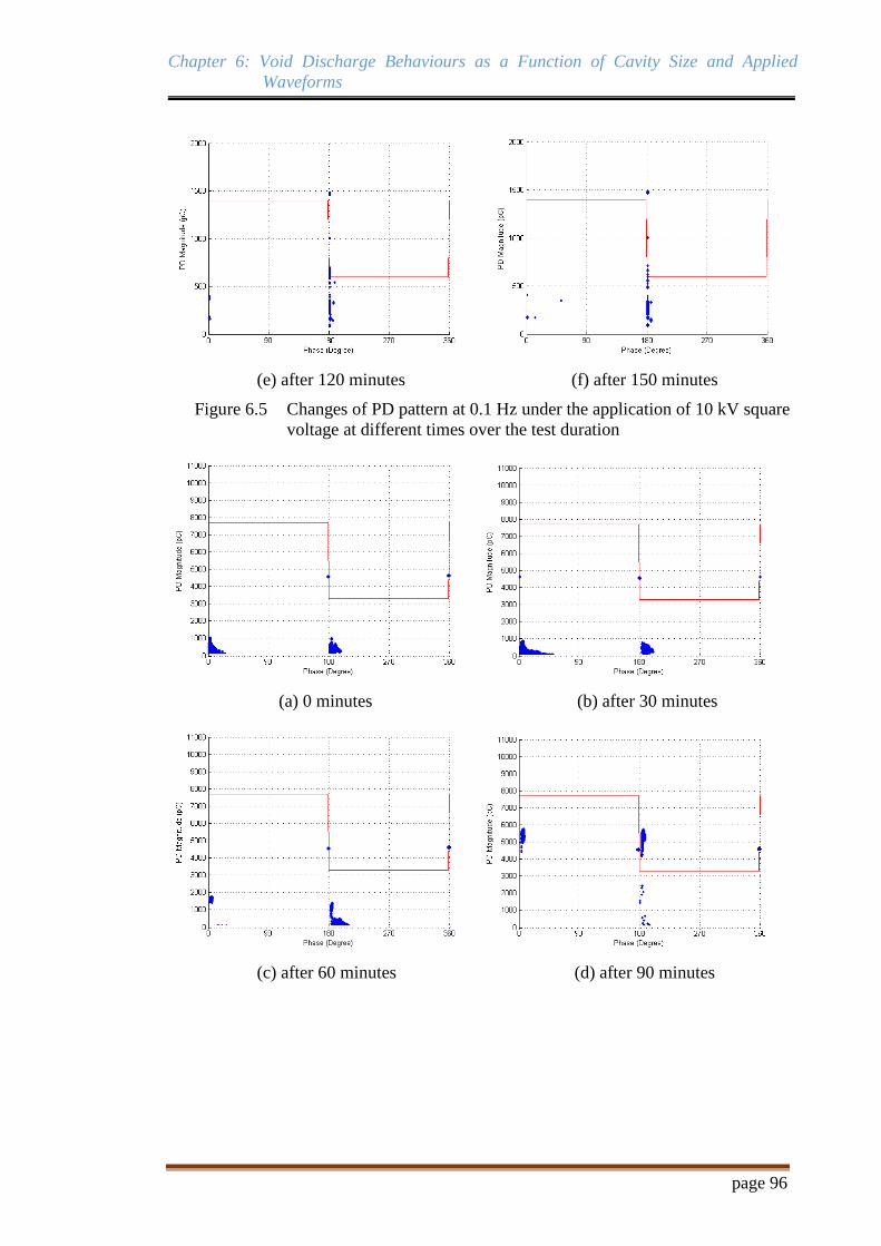
Chapter 6: Void Discharge Behaviours as a Function of Cavity Size and Applied
Waveforms
page 96
(e) after 120 minutes (f) after 150 minutes
Figure 6.5 Changes of PD pattern at 0.1 Hz under the application of 10 kV square
voltage at different times over the test duration
(a) 0 minutes (b) after 30 minutes
(c) after 60 minutes (d) after 90 minutes

Chapter 6: Void Discharge Behaviours as a Function of Cavity Size and Applied
Waveforms
page 97
(e) after 120 minutes (f) after 150 minutes
Figure 6.6 Changes of PD pattern at 50 Hz under the application of 10 kV square
voltage at different times over the test duration
The substantial difference of time duration of aging stages due to PDs could
be explained by variation of the local electric field inside the void because of
chemical and physical changes. At 50 Hz, the byproducts generated from
discharges are gradually deposited on the void surface; hence void surface
conductivity is changed progressively during the discharge period. Accumulated
charges and byproducts perform as a shield to slightly reduce the local electric
field in the void. Therefore, the PD magnitude tends to reduce over time in the
first stage.
Figure 6.7 Average PD magnitude over the testing period at 0.1 Hz and 50 Hz
under square voltage application of 10 kV
0
1000
2000
3000
4000
5000
6000
0 30 60 90 120 150
PD
Mag
nit
ud
e (p
C)
Time (minutes)
0.1 Hz
50 Hz
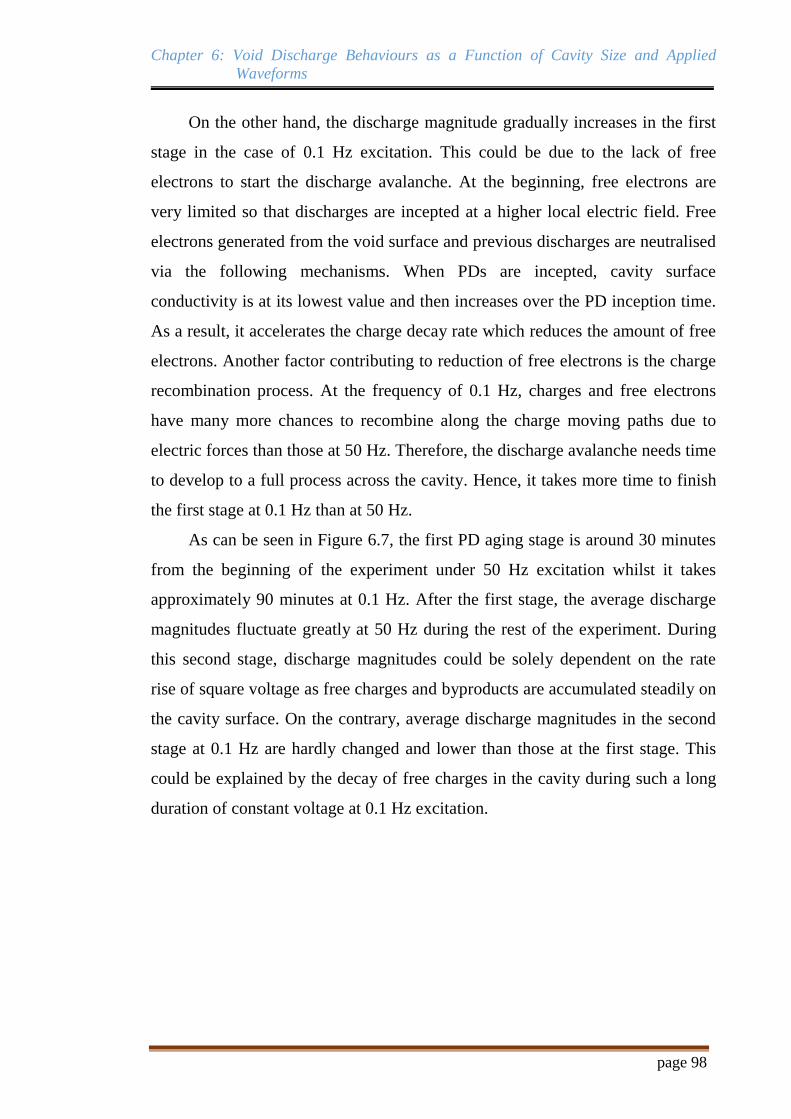
Chapter 6: Void Discharge Behaviours as a Function of Cavity Size and Applied
Waveforms
page 98
On the other hand, the discharge magnitude gradually increases in the first
stage in the case of 0.1 Hz excitation. This could be due to the lack of free
electrons to start the discharge avalanche. At the beginning, free electrons are
very limited so that discharges are incepted at a higher local electric field. Free
electrons generated from the void surface and previous discharges are neutralised
via the following mechanisms. When PDs are incepted, cavity surface
conductivity is at its lowest value and then increases over the PD inception time.
As a result, it accelerates the charge decay rate which reduces the amount of free
electrons. Another factor contributing to reduction of free electrons is the charge
recombination process. At the frequency of 0.1 Hz, charges and free electrons
have many more chances to recombine along the charge moving paths due to
electric forces than those at 50 Hz. Therefore, the discharge avalanche needs time
to develop to a full process across the cavity. Hence, it takes more time to finish
the first stage at 0.1 Hz than at 50 Hz.
As can be seen in Figure 6.7, the first PD aging stage is around 30 minutes
from the beginning of the experiment under 50 Hz excitation whilst it takes
approximately 90 minutes at 0.1 Hz. After the first stage, the average discharge
magnitudes fluctuate greatly at 50 Hz during the rest of the experiment. During
this second stage, discharge magnitudes could be solely dependent on the rate
rise of square voltage as free charges and byproducts are accumulated steadily on
the cavity surface. On the contrary, average discharge magnitudes in the second
stage at 0.1 Hz are hardly changed and lower than those at the first stage. This
could be explained by the decay of free charges in the cavity during such a long
duration of constant voltage at 0.1 Hz excitation.
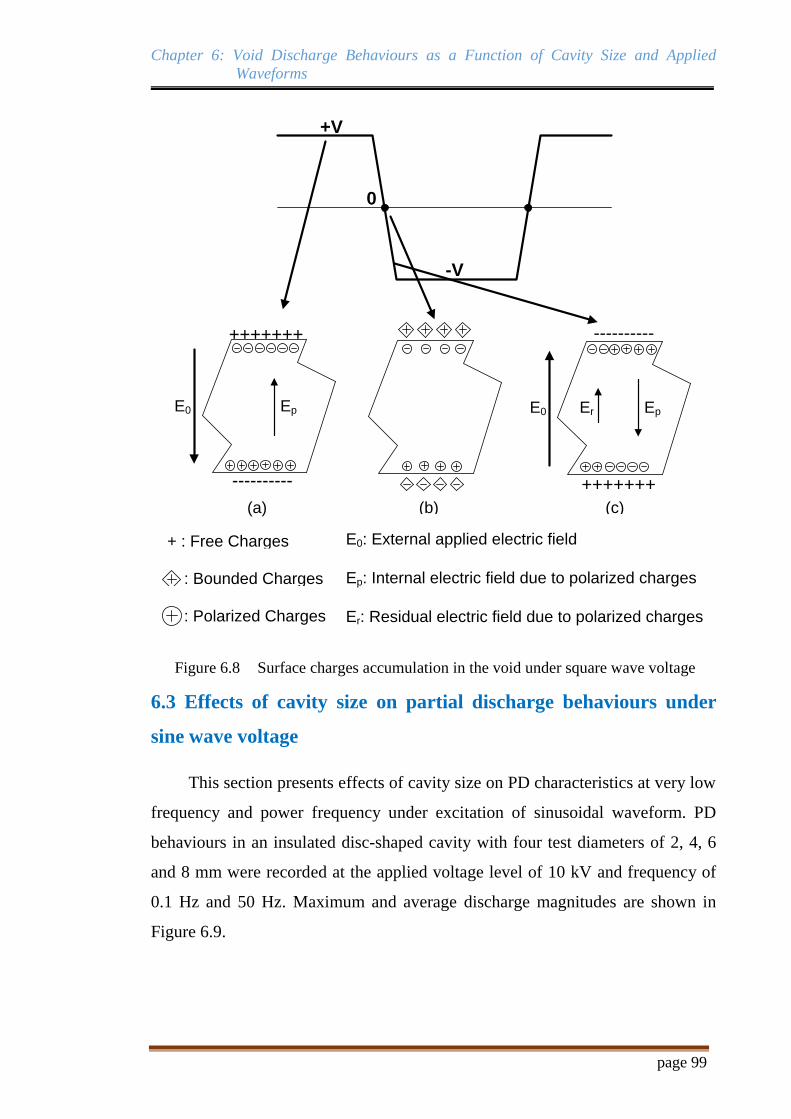
Chapter 6: Void Discharge Behaviours as a Function of Cavity Size and Applied
Waveforms
page 99
----------
0
-V
+V
ErEpE0
+++++++
EpE0
----------
+++++++
+ : Free Charges
: Bounded Charges
: Polarized Charges
(c)(b)(a)
E0: External applied electric field
Ep: Internal electric field due to polarized charges
Er: Residual electric field due to polarized charges
Figure 6.8 Surface charges accumulation in the void under square wave voltage
6.3 Effects of cavity size on partial discharge behaviours under
sine wave voltage
This section presents effects of cavity size on PD characteristics at very low
frequency and power frequency under excitation of sinusoidal waveform. PD
behaviours in an insulated disc-shaped cavity with four test diameters of 2, 4, 6
and 8 mm were recorded at the applied voltage level of 10 kV and frequency of
0.1 Hz and 50 Hz. Maximum and average discharge magnitudes are shown in
Figure 6.9.

Chapter 6: Void Discharge Behaviours as a Function of Cavity Size and Applied
Waveforms
page 100
(a) Maximum magnitude
(b) Average magnitude
Figure 6.9 PD magnitudes as a function of cavity size at 0.1 Hz and 50 Hz
As can be seen in Figure 6.9, the maximum discharge gradually increases
when the cavity size is larger at both frequencies. This may be due to the
availability of free charges generated in the void. With increased void diameter,
the cavity surface which is perpendicular to the electric field is larger, thus it can
emit more free charges under the effect of applied voltage. Therefore, PD
inception level is decreased when the void size is increased. Consequently, under
the same applied voltage, PDs in larger voids are ignited at a higher overvoltage
ratio compared to inception voltage, which results in larger discharge
magnitudes. Note that the cavity depth is unchanged, therefore the relative field
distribution in the void and in the solid insulation above and below it is not
affected and so the inception voltage is not affected by the cavity size. The
0
500
1000
1500
2000
2500
3000
3500
4000
4500
2 4 6 8
Dis
char
ge m
agn
itu
de
(pC
)
Void diameter (mm)
0.1 Hz
50 Hz
0
200
400
600
800
1000
1200
1400
2 4 6 8
Dis
char
ge m
agn
itu
de
(pC
)
Void diameter (mm)
0.1 Hz
50 Hz

Chapter 6: Void Discharge Behaviours as a Function of Cavity Size and Applied
Waveforms
page 101
simulation of electric field distribution in test samples at the positive voltage
peak, at time of 5 ms, is shown in Figure 6.10. Simulation results show that the
field distribution in test samples with various void size is almost identical.
Hence, Figure 6.10a shows only the electric field and potential distribution in the
sample with diameter of 2 mm. Field values along the axis of symmetry parallel
to the electric field, i.e. the z-axis, are plotted in Figure 6.10b for all test samples.
It is interesting to observe that average discharge magnitude at very low
frequency increases with the void size whilst it is slightly reduced when the void
diameter is larger than 4 mm at frequency of 50 Hz as in Figure 6.9b. This could
be explained by effects of surface charges on PD activities. At very low
frequency, more space charges generated after a PD are likely to decay as the
time span between two consecutive discharges is considerably large, i.e. in the
order of hundreds of milliseconds. Hence, it reduces the electron generation rate
igniting the following discharge. As a result, the next PD has a higher possibility
of being incepted at a voltage level higher than the inception value which gives
larger discharge magnitudes. On the other hand, the statistical time lag at 50 Hz
is much shorter than at very low frequency so free charges generated after a
discharge are less likely to decay. Therefore, when the local electric field
recovers and exceeds the critical inception value, the large electron generation
rate available presents a favourable condition for discharges to be incepted.
According to measurements, many discharges with low magnitudes were
recorded, which implies discharges are incepted very soon as the critical
inception value is exceeded as available electrons are abundant in this moment.
As the void size is increased, the discharge area is enlarged and thus the
accumulated charge distribution may not be uniform over the whole surface area.
Thus, there could be multiple charge concentration points on the cavity surface
which enables multiple discharges to be ignited simultaneously. This also
explained the increase of PD repetition rate when the cavity diameter is larger.

Chapter 6: Void Discharge Behaviours as a Function of Cavity Size and Applied
Waveforms
page 102
(a) Field and potential distribution in sample 1 with diameter of 2 mm
(b) Field values along the z-axis
Figure 6.10 Electric field distribution in test samples
6.4 Effects of voltage waveforms on partial discharge behaviours
In this section, test sample 1 with a void diameter of 2 mm was used to
investigate PD behaviours under different applied voltage waveforms including
traditional sine wave and trapezoid-based wave. Parameters for the trapezoid-
based waveform are shown in Figure 6.11: a symmetric trapezoidal wave with
equal linear rising and falling edge period is shown in trace (b), i.e. t1 = t3, and a
symmetric triangle wave is shown in trace (a), i.e. t2 = 0.
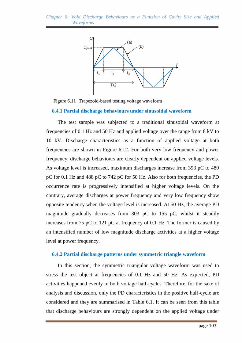
Chapter 6: Void Discharge Behaviours as a Function of Cavity Size and Applied
Waveforms
page 103
U
Upeak
t1
T/2
t2 t3
(a)(b)
t
Figure 6.11 Trapezoid-based testing voltage waveform
6.4.1 Partial discharge behaviours under sinusoidal waveform
The test sample was subjected to a traditional sinusoidal waveform at
frequencies of 0.1 Hz and 50 Hz and applied voltage over the range from 8 kV to
10 kV. Discharge characteristics as a function of applied voltage at both
frequencies are shown in Figure 6.12. For both very low frequency and power
frequency, discharge behaviours are clearly dependent on applied voltage levels.
As voltage level is increased, maximum discharges increase from 393 pC to 480
pC for 0.1 Hz and 488 pC to 742 pC for 50 Hz. Also for both frequencies, the PD
occurrence rate is progressively intensified at higher voltage levels. On the
contrary, average discharges at power frequency and very low frequency show
opposite tendency when the voltage level is increased. At 50 Hz, the average PD
magnitude gradually decreases from 303 pC to 155 pC, whilst it steadily
increases from 75 pC to 121 pC at frequency of 0.1 Hz. The former is caused by
an intensified number of low magnitude discharge activities at a higher voltage
level at power frequency.
6.4.2 Partial discharge patterns under symmetric triangle waveform
In this section, the symmetric triangular voltage waveform was used to
stress the test object at frequencies of 0.1 Hz and 50 Hz. As expected, PD
activities happened evenly in both voltage half-cycles. Therefore, for the sake of
analysis and discussion, only the PD characteristics in the positive half-cycle are
considered and they are summarised in Table 6.1. It can be seen from this table
that discharge behaviours are strongly dependent on the applied voltage under
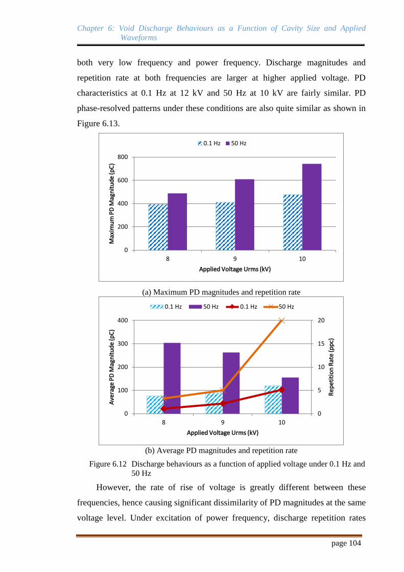
Chapter 6: Void Discharge Behaviours as a Function of Cavity Size and Applied
Waveforms
page 104
both very low frequency and power frequency. Discharge magnitudes and
repetition rate at both frequencies are larger at higher applied voltage. PD
characteristics at 0.1 Hz at 12 kV and 50 Hz at 10 kV are fairly similar. PD
phase-resolved patterns under these conditions are also quite similar as shown in
Figure 6.13.
(a) Maximum PD magnitudes and repetition rate
(b) Average PD magnitudes and repetition rate
Figure 6.12 Discharge behaviours as a function of applied voltage under 0.1 Hz and
50 Hz
However, the rate of rise of voltage is greatly different between these
frequencies, hence causing significant dissimilarity of PD magnitudes at the same
voltage level. Under excitation of power frequency, discharge repetition rates
0
200
400
600
800
8 9 10
Max
imu
m P
D M
agn
itu
de
(pC
)
Applied Voltage Urms (kV)
0.1 Hz 50 Hz
0
5
10
15
20
0
100
200
300
400
8 9 10
Re
pet
itio
n R
ate
(pp
c)
Ave
rage
PD
Mag
nit
ud
e (p
C)
Applied Voltage Urms (kV)
0.1 Hz 50 Hz 0.1 Hz 50 Hz
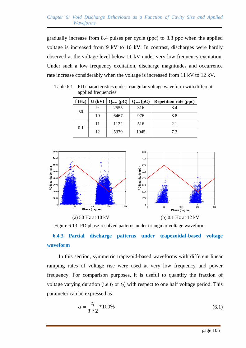
Chapter 6: Void Discharge Behaviours as a Function of Cavity Size and Applied
Waveforms
page 105
gradually increase from 8.4 pulses per cycle (ppc) to 8.8 ppc when the applied
voltage is increased from 9 kV to 10 kV. In contrast, discharges were hardly
observed at the voltage level below 11 kV under very low frequency excitation.
Under such a low frequency excitation, discharge magnitudes and occurrence
rate increase considerably when the voltage is increased from 11 kV to 12 kV.
Table 6.1 PD characteristics under triangular voltage waveform with different
applied frequencies
f (Hz) U (kV) Qmax (pC) Qave (pC) Repetition rate (ppc)
50 9 2555 316 8.4
10 6467 976 8.8
0.1 11 1122 516 2.1
12 5379 1045 7.3
(a) 50 Hz at 10 kV (b) 0.1 Hz at 12 kV
Figure 6.13 PD phase-resolved patterns under triangular voltage waveform
6.4.3 Partial discharge patterns under trapezoidal-based voltage
waveform
In this section, symmetric trapezoid-based waveforms with different linear
ramping rates of voltage rise were used at very low frequency and power
frequency. For comparison purposes, it is useful to quantify the fraction of
voltage varying duration (i.e t1 or t3) with respect to one half voltage period. This
parameter can be expressed as:
1 *100%/ 2
t
T (6.1)
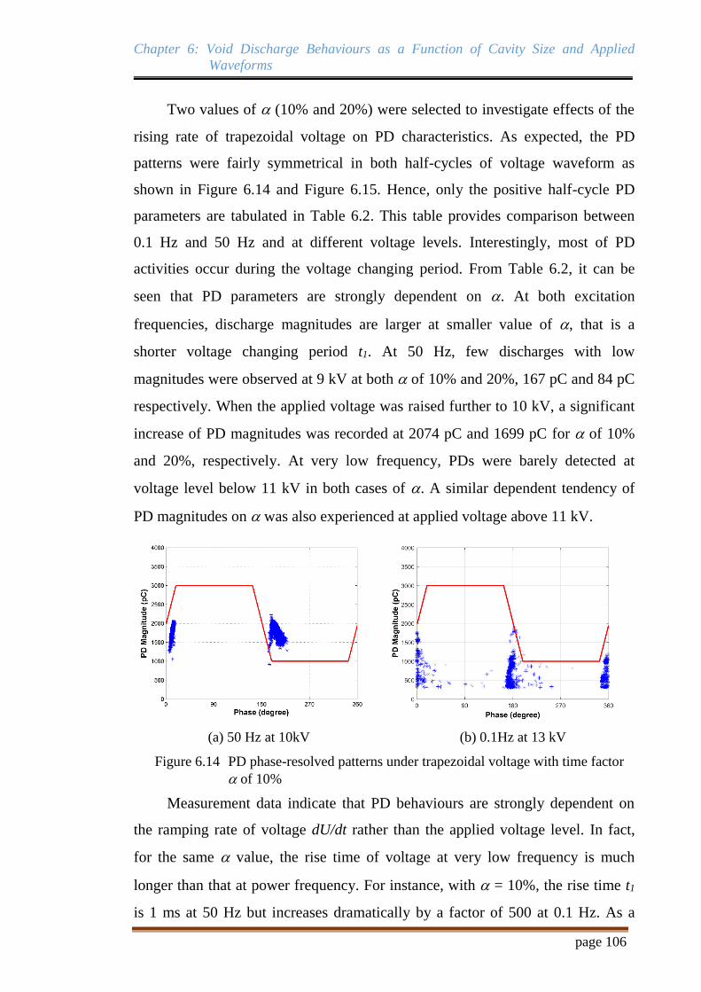
Chapter 6: Void Discharge Behaviours as a Function of Cavity Size and Applied
Waveforms
page 106
Two values of (10% and 20%) were selected to investigate effects of the
rising rate of trapezoidal voltage on PD characteristics. As expected, the PD
patterns were fairly symmetrical in both half-cycles of voltage waveform as
shown in Figure 6.14 and Figure 6.15. Hence, only the positive half-cycle PD
parameters are tabulated in Table 6.2. This table provides comparison between
0.1 Hz and 50 Hz and at different voltage levels. Interestingly, most of PD
activities occur during the voltage changing period. From Table 6.2, it can be
seen that PD parameters are strongly dependent on . At both excitation
frequencies, discharge magnitudes are larger at smaller value of , that is a
shorter voltage changing period t1. At 50 Hz, few discharges with low
magnitudes were observed at 9 kV at both of 10% and 20%, 167 pC and 84 pC
respectively. When the applied voltage was raised further to 10 kV, a significant
increase of PD magnitudes was recorded at 2074 pC and 1699 pC for of 10%
and 20%, respectively. At very low frequency, PDs were barely detected at
voltage level below 11 kV in both cases of . A similar dependent tendency of
PD magnitudes on was also experienced at applied voltage above 11 kV.
(a) 50 Hz at 10kV (b) 0.1Hz at 13 kV
Figure 6.14 PD phase-resolved patterns under trapezoidal voltage with time factor
of 10%
Measurement data indicate that PD behaviours are strongly dependent on
the ramping rate of voltage dU/dt rather than the applied voltage level. In fact,
for the same value, the rise time of voltage at very low frequency is much
longer than that at power frequency. For instance, with = 10%, the rise time t1
is 1 ms at 50 Hz but increases dramatically by a factor of 500 at 0.1 Hz. As a
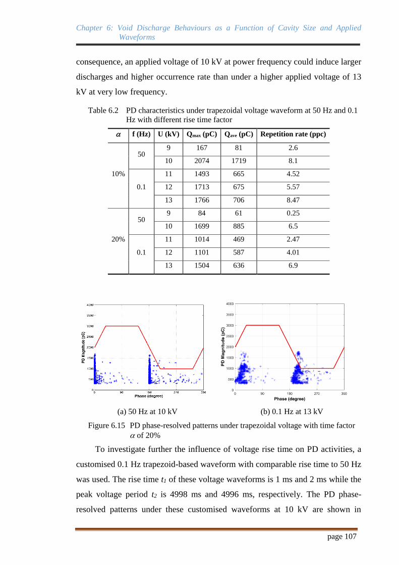
Chapter 6: Void Discharge Behaviours as a Function of Cavity Size and Applied
Waveforms
page 107
consequence, an applied voltage of 10 kV at power frequency could induce larger
discharges and higher occurrence rate than under a higher applied voltage of 13
kV at very low frequency.
Table 6.2 PD characteristics under trapezoidal voltage waveform at 50 Hz and 0.1
Hz with different rise time factor
f (Hz) U (kV) Qmax (pC) Qave (pC) Repetition rate (ppc)
10%
50 9 167 81 2.6
10 2074 1719 8.1
0.1
11 1493 665 4.52
12 1713 675 5.57
13 1766 706 8.47
20%
50 9 84 61 0.25
10 1699 885 6.5
0.1
11 1014 469 2.47
12 1101 587 4.01
13 1504 636 6.9
(a) 50 Hz at 10 kV (b) 0.1 Hz at 13 kV
Figure 6.15 PD phase-resolved patterns under trapezoidal voltage with time factor
of 20%
To investigate further the influence of voltage rise time on PD activities, a
customised 0.1 Hz trapezoid-based waveform with comparable rise time to 50 Hz
was used. The rise time t1 of these voltage waveforms is 1 ms and 2 ms while the
peak voltage period t2 is 4998 ms and 4996 ms, respectively. The PD phase-
resolved patterns under these customised waveforms at 10 kV are shown in
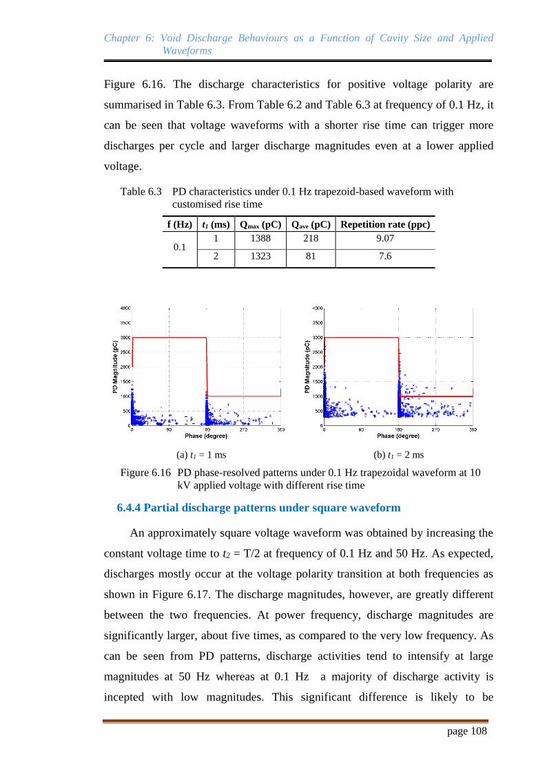
Chapter 6: Void Discharge Behaviours as a Function of Cavity Size and Applied
Waveforms
page 108
Figure 6.16. The discharge characteristics for positive voltage polarity are
summarised in Table 6.3. From Table 6.2 and Table 6.3 at frequency of 0.1 Hz, it
can be seen that voltage waveforms with a shorter rise time can trigger more
discharges per cycle and larger discharge magnitudes even at a lower applied
voltage.
Table 6.3 PD characteristics under 0.1 Hz trapezoid-based waveform with
customised rise time
f (Hz) t1 (ms) Qmax (pC) Qave (pC) Repetition rate (ppc)
0.1 1 1388 218 9.07
2 1323 81 7.6
(a) t1 = 1 ms (b) t1 = 2 ms
Figure 6.16 PD phase-resolved patterns under 0.1 Hz trapezoidal waveform at 10
kV applied voltage with different rise time
6.4.4 Partial discharge patterns under square waveform
An approximately square voltage waveform was obtained by increasing the
constant voltage time to t2 = T/2 at frequency of 0.1 Hz and 50 Hz. As expected,
discharges mostly occur at the voltage polarity transition at both frequencies as
shown in Figure 6.17. The discharge magnitudes, however, are greatly different
between the two frequencies. At power frequency, discharge magnitudes are
significantly larger, about five times, as compared to the very low frequency. As
can be seen from PD patterns, discharge activities tend to intensify at large
magnitudes at 50 Hz whereas at 0.1 Hz a majority of discharge activity is
incepted with low magnitudes. This significant difference is likely to be
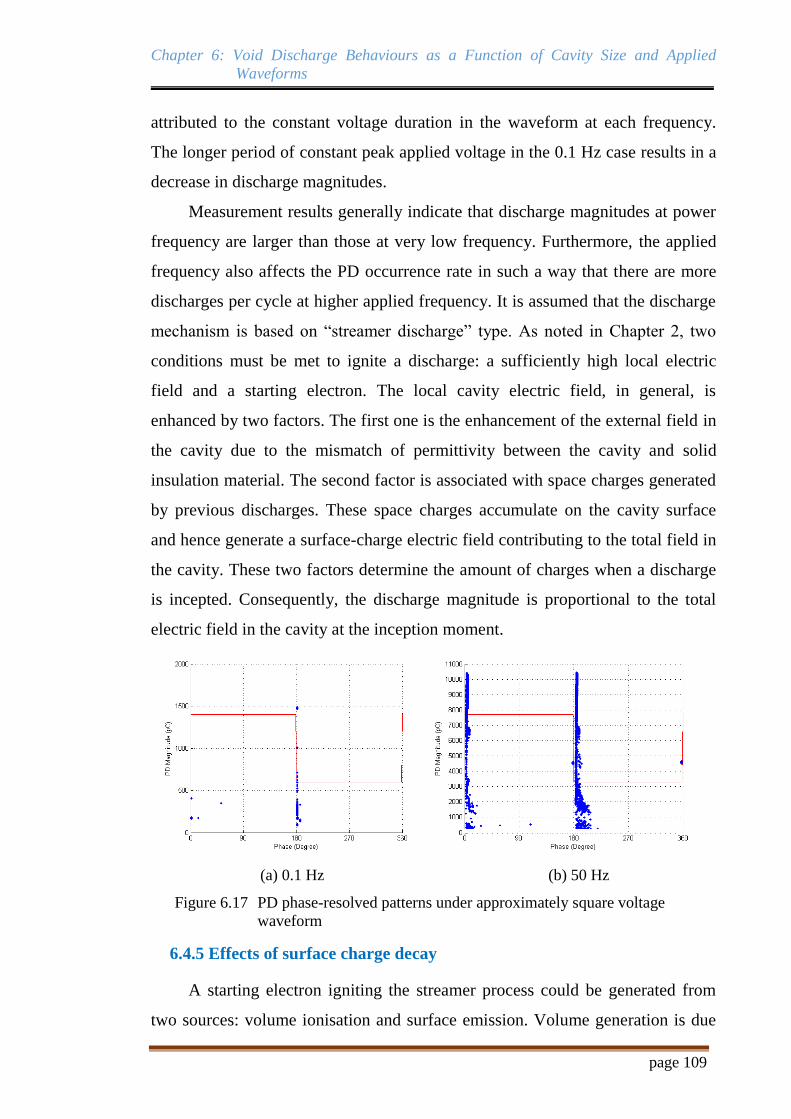
Chapter 6: Void Discharge Behaviours as a Function of Cavity Size and Applied
Waveforms
page 109
attributed to the constant voltage duration in the waveform at each frequency.
The longer period of constant peak applied voltage in the 0.1 Hz case results in a
decrease in discharge magnitudes.
Measurement results generally indicate that discharge magnitudes at power
frequency are larger than those at very low frequency. Furthermore, the applied
frequency also affects the PD occurrence rate in such a way that there are more
discharges per cycle at higher applied frequency. It is assumed that the discharge
mechanism is based on “streamer discharge” type. As noted in Chapter 2, two
conditions must be met to ignite a discharge: a sufficiently high local electric
field and a starting electron. The local cavity electric field, in general, is
enhanced by two factors. The first one is the enhancement of the external field in
the cavity due to the mismatch of permittivity between the cavity and solid
insulation material. The second factor is associated with space charges generated
by previous discharges. These space charges accumulate on the cavity surface
and hence generate a surface-charge electric field contributing to the total field in
the cavity. These two factors determine the amount of charges when a discharge
is incepted. Consequently, the discharge magnitude is proportional to the total
electric field in the cavity at the inception moment.
(a) 0.1 Hz (b) 50 Hz
Figure 6.17 PD phase-resolved patterns under approximately square voltage
waveform
6.4.5 Effects of surface charge decay
A starting electron igniting the streamer process could be generated from
two sources: volume ionisation and surface emission. Volume generation is due
Chapter 6: Void Discharge Behaviours as a Function of Cavity Size and Applied
Waveforms
page 110
to gas ionisation by photon impact and field detachment of electrons from
negative charges. The second process is electron emission from the cavity
surface, which includes electrons detrapped from shallow traps at the surface,
electron generation by ion collision and the surface photo effect. The source of
starting electrons is greatly enhanced by free charges generated after a discharge.
As the cavity surface has a finite value of conductivity, surface deposited charges
decay with time by drifting into deeper traps, by a recombination process or by
moving along the cavity wall under the effects of the local electric field. This
decay rate is commonly represented by the average charge decay time constant
decay.
Differences in PD characteristics observed in the measurement results may
be attributed to the charge decay rate. If decay is smaller than the duration of the
applied voltage period, i.e. decay << 1/f , it is assumed that most of the free
charges have already decayed and thus surface deposited charges are not
contributing much in the PD process. On the other hand, if the decay time is
longer than the voltage period, i.e decay >> 1/f , charges are not decayed and will
make a significant contribution to the total field in the cavity. In this case,
discharge magnitudes are strongly dependent on the applied frequency as seen in
Section 6.4.1. At frequency of 50 Hz, free charges are not decayed between two
consecutive discharges and hence PDs would be incepted at the instant when the
local field exceeds the critical value. Consequently, more discharges with low
magnitudes are produced at higher applied voltage.
The effect of charge decay under a trapezoid-based applied waveform is
illustrated in Figure 6.18. Here, it is assumed that a residual electric field does
not exist initially; the cavity field, i.e. Ecav (blue straight line), is equivalent to the
external field associated with the applied voltage, E0 (black dashed line). A
discharge will be incepted when Ecav is larger than the inception value, Einc, and a
starting electron is available. During the discharge process, the cavity field is
dropping rapidly and stops at the residual value Eres lower than the extinction
value, Eext, which determines the PD ceased condition. Free charges released
after a PD process deposit on the cavity surface and then produce an electric
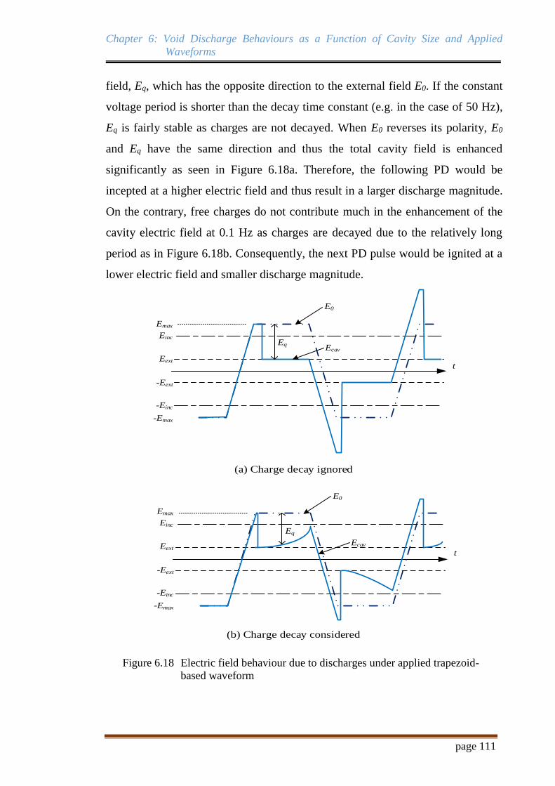
Chapter 6: Void Discharge Behaviours as a Function of Cavity Size and Applied
Waveforms
page 111
field, Eq, which has the opposite direction to the external field E0. If the constant
voltage period is shorter than the decay time constant (e.g. in the case of 50 Hz),
Eq is fairly stable as charges are not decayed. When E0 reverses its polarity, E0
and Eq have the same direction and thus the total cavity field is enhanced
significantly as seen in Figure 6.18a. Therefore, the following PD would be
incepted at a higher electric field and thus result in a larger discharge magnitude.
On the contrary, free charges do not contribute much in the enhancement of the
cavity electric field at 0.1 Hz as charges are decayed due to the relatively long
period as in Figure 6.18b. Consequently, the next PD pulse would be ignited at a
lower electric field and smaller discharge magnitude.
t
t
E0
Ecav
Eq
Einc
-Einc
Eext
-Eext
Emax
-Emax
E0
Ecav
Eq
Einc
-Einc
Eext
-Eext
Emax
-Emax
(a) Charge decay ignored
(b) Charge decay considered
Figure 6.18 Electric field behaviour due to discharges under applied trapezoid-
based waveform
Chapter 6: Void Discharge Behaviours as a Function of Cavity Size and Applied
Waveforms
page 112
6.5 Conclusion
This chapter reported a comparative study of internal discharges in a
cylindrical cavity bounded by solid insulation material as a function of cavity
size and applied voltage waveforms at very low frequency and power frequency.
Changes of PD characteristics after long discharge exposure under excitation of
sinusoidal and square waveforms were discussed in detail at both frequencies.
Various waveforms including sinusoidal and trapezoid-based type were
employed to stress the test samples. Various PD characteristics (magnitude,
repetition rate, phase-resolved patterns) were analyzed. It is concluded that PD
behaviors are strongly dependent on the applied frequency and the slew rate of
voltage. PD magnitudes at very low frequency are generally lower than those at
power frequency excitation regardless of applied voltage waveforms. A larger
cavity could also lead to more discharges with low magnitudes as the discharge
surface area is increased. The main reason for these behaviours is the
contribution of the charge decay mechanism in the enhancement of the cavity
field. Charge decay plays a significant impact on PD characteristics at 0.1 Hz. In
the following chapter, the measurement results of partial discharge in a cavity are
used to compare with computer simulation data to determine critical parameters
affecting discharge behaviours, especially the decay of accumulated charges on
the cavity surface.
page 113
Chapter 7: Void Discharge
Behaviours: Comparison between
Measurements and Simulations
7.1 Introduction
This chapter describes PD and electric field behaviours obtained from a
simulation model and compares measurement data with simulated results. The
physical progress of the electric field in the cavity is discussed together with the
PD magnitude when discharges occur. From the simulation model, critical
parameters that significantly influence PD events can be identified. Cycle to
cycle PD behaviours are investigated through simulation of the electric field and
PD events against time. The statistical time lag of PD activities can be calculated
at very low frequency and power frequency at different applied voltages to
consider dependence on applied frequency and voltage amplitudes.
Section 7.2 presents the simulation results obtained from the partial
discharge model. In Section 7.3, the model is then verified with the measured
data from experiments at very low frequency and power frequency as a function
of applied voltage amplitudes. This verification enables the calculation of key
parameters affecting partial discharge behaviours such as the statistical time lag
which is reported in Section 7.4.
7.2 Results from simulation model
7.2.1 Electric field distribution in the model
The equipotential lines and electric field distribution in the simulated model
just before and after the first PD are shown in Figure 7.1. The cavity which is
cylindrical with a radius of 1 mm and height of 1 mm is within the insulation

Chapter 7: Void Discharge Behaviours: Comparison between Measurements and
Simulations
page 114
material with thickness of 3 mm. The model is simulated at frequency of 50 Hz
and applied voltage of 10 kVrms. As can be seen in Figure 7.1a, the electric field
in the cavity before the PD event is much higher than the surrounding area of
material because the relative permittivity of the cavity is lower than that of the
insulation material. This is presented with the yellow-red colour scale in the
cavity area with more closely packed equipotential lines.
(a) Before the first PD occurrence
(b) After the first PD occurrence
Figure 7.1 Simulation of electric field distribution and equipotential lines in the
model at 50 Hz and 10 kVrms when the first PD occurs
Furthermore, the electric field is highest at the void surfaces closest to the
electrodes as the applied field is nearly perpendicular to the surfaces. This can be
observed in the cross-section plot of electric field magnitude along the z-axis of
the model in Figure 7.2a. The field distribution is not homogeneous but
symmetrical along the z-axis as the cavity size is comparably large relative to the
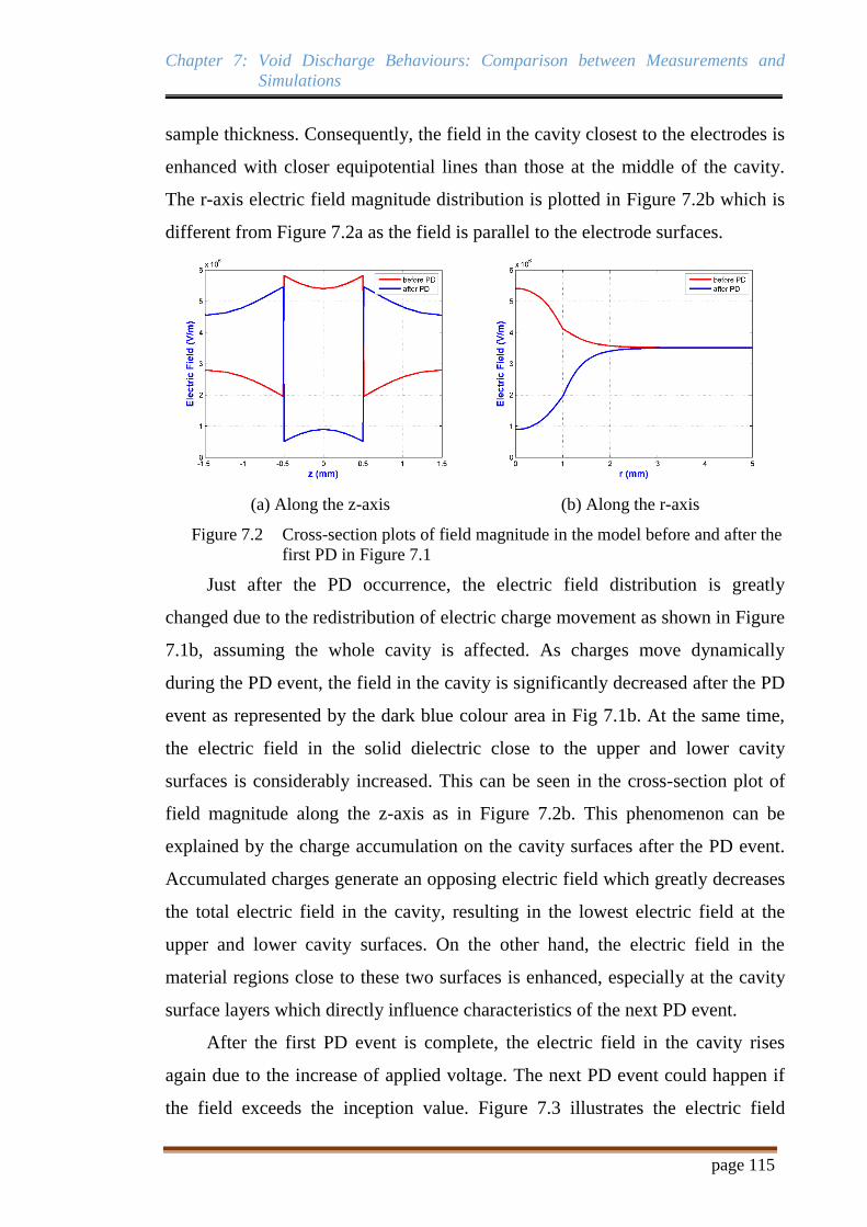
Chapter 7: Void Discharge Behaviours: Comparison between Measurements and
Simulations
page 115
sample thickness. Consequently, the field in the cavity closest to the electrodes is
enhanced with closer equipotential lines than those at the middle of the cavity.
The r-axis electric field magnitude distribution is plotted in Figure 7.2b which is
different from Figure 7.2a as the field is parallel to the electrode surfaces.
(a) Along the z-axis (b) Along the r-axis
Figure 7.2 Cross-section plots of field magnitude in the model before and after the
first PD in Figure 7.1
Just after the PD occurrence, the electric field distribution is greatly
changed due to the redistribution of electric charge movement as shown in Figure
7.1b, assuming the whole cavity is affected. As charges move dynamically
during the PD event, the field in the cavity is significantly decreased after the PD
event as represented by the dark blue colour area in Fig 7.1b. At the same time,
the electric field in the solid dielectric close to the upper and lower cavity
surfaces is considerably increased. This can be seen in the cross-section plot of
field magnitude along the z-axis as in Figure 7.2b. This phenomenon can be
explained by the charge accumulation on the cavity surfaces after the PD event.
Accumulated charges generate an opposing electric field which greatly decreases
the total electric field in the cavity, resulting in the lowest electric field at the
upper and lower cavity surfaces. On the other hand, the electric field in the
material regions close to these two surfaces is enhanced, especially at the cavity
surface layers which directly influence characteristics of the next PD event.
After the first PD event is complete, the electric field in the cavity rises
again due to the increase of applied voltage. The next PD event could happen if
the field exceeds the inception value. Figure 7.3 illustrates the electric field

Chapter 7: Void Discharge Behaviours: Comparison between Measurements and
Simulations
page 116
distribution and equipotential lines in the simulation model when the second PD
occurs. Figure 7.4 shows the cross-section plots of electric field magnitude along
the z-axis and r-axis.
(a) Before the second PD occurrence
(b) After the second PD occurrence
Figure 7.3 Simulation of electric field distribution and equipotential lines in the
model at 50 Hz and 10 kVrms when the second PD occurs
As shown in Figure 7.3a, the electric field in the cavity is significantly large
compared with Figure 7.1a, presenting with the dark red colour scale and highly
dense equipotential lines. This could be explained by the effect of accumulated
charges on the upper and lower cavity surfaces when the voltage polarity
changes. Note that the first and second PD occur in different half-cycles (i.e. at
2.68 ms and 12.76 ms, respectively), so that the external electric field due to
applied voltage alters and has the same direction with the field due to surface
accumulated charges in the cavity. As a result, the total electric field in the cavity

Chapter 7: Void Discharge Behaviours: Comparison between Measurements and
Simulations
page 117
is significantly enhanced. This effect can also be observed in Figure 7.4a with the
electric field fluctuation at the cavity surface layer (the depth of 0.1 mm in the
model) between the insulation material and the cavity. After the second PD, the
electric field has similar trends to the first PD. Since free charges generated from
the first PD still deposit on the cavity surface when the second PD is incepted,
the amount of surface charges is considerably increased just after the second PD
occurs. Consequently, the electric field on the upper and lower surface of cavity
is higher as can be seen in Fig 7.4a (6.20 MV/m vs 5.46 MV/m in Fig 7.2a).
(a) Along the z-axis (b) Along the r-axis
Figure 7.4 Cross-section plots of field magnitude in the model before and after the
second PD in Figure 7.3
The model is also simulated at frequency of 0.1 Hz (and same applied
voltage of 10 kVrms) for comparison. Similar distributions of electric field and
equipotential lines to simulation results of 50 Hz are also observed at the first PD
occurrence as shown in Figure 7.5 and Figure 7.6. The electric field in the cavity
is enhanced due to the mismatch of the relative permittivity of air in the cavity
and solid insulation material as can be seen in the light yellow colour scale in
Figure 7.5a. Once the first PD is incepted, the electric field in the cavity reduces
significantly as in Figure 7.5b with the dark blue colour scale. The solid
dielectric areas closest to the upper and lower cavity surfaces have the highest
electric field magnitude distribution as shown in Figure 7.6a.
After the first PD occurrence, the applied voltage continues increasing,
resulting in the increase of electric field distribution in the dielectric material as
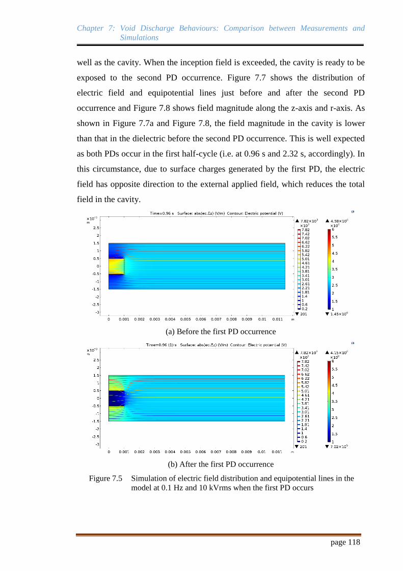
Chapter 7: Void Discharge Behaviours: Comparison between Measurements and
Simulations
page 118
well as the cavity. When the inception field is exceeded, the cavity is ready to be
exposed to the second PD occurrence. Figure 7.7 shows the distribution of
electric field and equipotential lines just before and after the second PD
occurrence and Figure 7.8 shows field magnitude along the z-axis and r-axis. As
shown in Figure 7.7a and Figure 7.8, the field magnitude in the cavity is lower
than that in the dielectric before the second PD occurrence. This is well expected
as both PDs occur in the first half-cycle (i.e. at 0.96 s and 2.32 s, accordingly). In
this circumstance, due to surface charges generated by the first PD, the electric
field has opposite direction to the external applied field, which reduces the total
field in the cavity.
(a) Before the first PD occurrence
(b) After the first PD occurrence
Figure 7.5 Simulation of electric field distribution and equipotential lines in the
model at 0.1 Hz and 10 kVrms when the first PD occurs
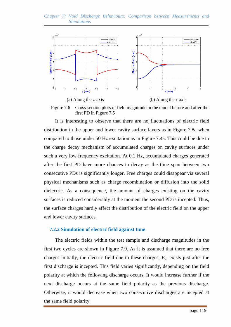
Chapter 7: Void Discharge Behaviours: Comparison between Measurements and
Simulations
page 119
(a) Along the z-axis (b) Along the r-axis
Figure 7.6 Cross-section plots of field magnitude in the model before and after the
first PD in Figure 7.5
It is interesting to observe that there are no fluctuations of electric field
distribution in the upper and lower cavity surface layers as in Figure 7.8a when
compared to those under 50 Hz excitation as in Figure 7.4a. This could be due to
the charge decay mechanism of accumulated charges on cavity surfaces under
such a very low frequency excitation. At 0.1 Hz, accumulated charges generated
after the first PD have more chances to decay as the time span between two
consecutive PDs is significantly longer. Free charges could disappear via several
physical mechanisms such as charge recombination or diffusion into the solid
dielectric. As a consequence, the amount of charges existing on the cavity
surfaces is reduced considerably at the moment the second PD is incepted. Thus,
the surface charges hardly affect the distribution of the electric field on the upper
and lower cavity surfaces.
7.2.2 Simulation of electric field against time
The electric fields within the test sample and discharge magnitudes in the
first two cycles are shown in Figure 7.9. As it is assumed that there are no free
charges initially, the electric field due to these charges, Eq, exists just after the
first discharge is incepted. This field varies significantly, depending on the field
polarity at which the following discharge occurs. It would increase further if the
next discharge occurs at the same field polarity as the previous discharge.
Otherwise, it would decrease when two consecutive discharges are incepted at
the same field polarity.
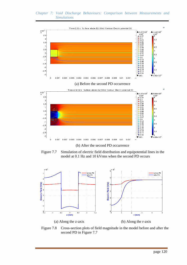
Chapter 7: Void Discharge Behaviours: Comparison between Measurements and
Simulations
page 120
(a) Before the second PD occurrence
(b) After the second PD occurrence
Figure 7.7 Simulation of electric field distribution and equipotential lines in the
model at 0.1 Hz and 10 kVrms when the second PD occurs
(a) Along the z-axis (b) Along the r-axis
Figure 7.8 Cross-section plots of field magnitude in the model before and after the
second PD in Figure 7.7

Chapter 7: Void Discharge Behaviours: Comparison between Measurements and
Simulations
page 121
Comparing the Eq behaviour due to local electric field polarity reversal at
0.1 Hz and 50 Hz, it is relatively easier to observe a slight decrease of Eq at very
low frequency excitation than at power frequency. This could be explained by the
effect of surface charge decay. When Ecav reverses polarity, mobility of charges
on the cavity wall is enhanced and exhibits an increase of cavity surface
conductivity. Thus, these charges decay with time and Eq is slightly reduced. As
a period duration at very low frequency is much longer than at power frequency,
the decrease of Eq is much greater at 0.1 Hz. Charge decay also affects the
moment the first PD is incepted after field polarity reversal. The availability of
starting electrons after the cavity field zero-crossing points is reduced due to
charge decay mechanisms and thus makes the first PD after polarity reversal
occur at a higher field which results in larger magnitudes.
(a) 0.1 Hz (b) 50 Hz
(c) 0.1 Hz (d) 50 Hz
Figure 7.9 Electric field and PD magnitude in the first two cycles at 0.1 Hz (a, c)
and 50 Hz (b, d)
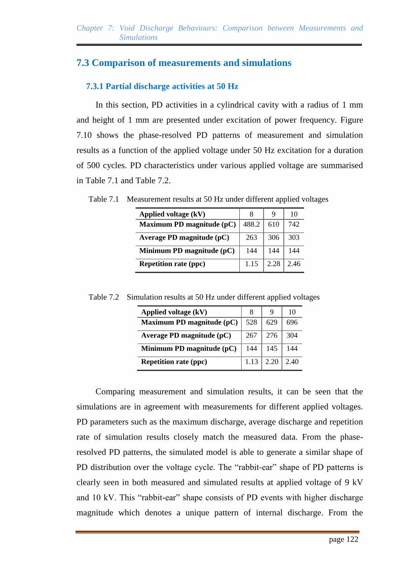
Chapter 7: Void Discharge Behaviours: Comparison between Measurements and
Simulations
page 122
7.3 Comparison of measurements and simulations
7.3.1 Partial discharge activities at 50 Hz
In this section, PD activities in a cylindrical cavity with a radius of 1 mm
and height of 1 mm are presented under excitation of power frequency. Figure
7.10 shows the phase-resolved PD patterns of measurement and simulation
results as a function of the applied voltage under 50 Hz excitation for a duration
of 500 cycles. PD characteristics under various applied voltage are summarised
in Table 7.1 and Table 7.2.
Table 7.1 Measurement results at 50 Hz under different applied voltages
Applied voltage (kV) 8 9 10
Maximum PD magnitude (pC) 488.2 610 742
Average PD magnitude (pC) 263 306 303
Minimum PD magnitude (pC) 144 144 144
Repetition rate (ppc) 1.15 2.28 2.46
Table 7.2 Simulation results at 50 Hz under different applied voltages
Applied voltage (kV) 8 9 10
Maximum PD magnitude (pC) 528 629 696
Average PD magnitude (pC) 267 276 304
Minimum PD magnitude (pC) 144 145 144
Repetition rate (ppc) 1.13 2.20 2.40
Comparing measurement and simulation results, it can be seen that the
simulations are in agreement with measurements for different applied voltages.
PD parameters such as the maximum discharge, average discharge and repetition
rate of simulation results closely match the measured data. From the phase-
resolved PD patterns, the simulated model is able to generate a similar shape of
PD distribution over the voltage cycle. The “rabbit-ear” shape of PD patterns is
clearly seen in both measured and simulated results at applied voltage of 9 kV
and 10 kV. This “rabbit-ear” shape consists of PD events with higher discharge
magnitude which denotes a unique pattern of internal discharge. From the
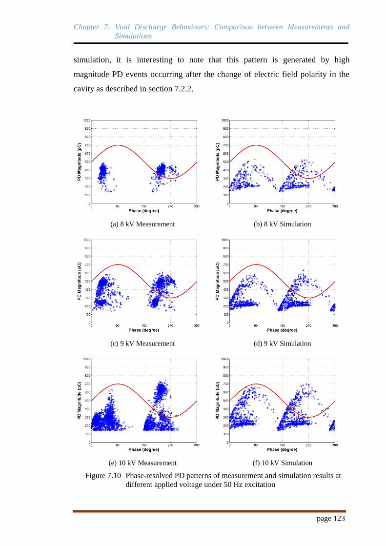
Chapter 7: Void Discharge Behaviours: Comparison between Measurements and
Simulations
page 123
simulation, it is interesting to note that this pattern is generated by high
magnitude PD events occurring after the change of electric field polarity in the
cavity as described in section 7.2.2.
(a) 8 kV Measurement (b) 8 kV Simulation
(c) 9 kV Measurement (d) 9 kV Simulation
(e) 10 kV Measurement (f) 10 kV Simulation
Figure 7.10 Phase-resolved PD patterns of measurement and simulation results at
different applied voltage under 50 Hz excitation

Chapter 7: Void Discharge Behaviours: Comparison between Measurements and
Simulations
page 124
When the polarity of the electric field changes between two consecutive
discharges, the magnitude of the electric field is enhanced significantly due to the
residual field of surface charges. Hence, the next PD event is incepted at higher
field magnitude which results in larger discharge magnitude. On the other hand,
the next PD occurs with lower magnitude when there is no field polarity
alternation. These discharges produce the broad “straight-line” shape in the
phase-resolved PD patterns. Also, a few discharges happened before the zero-
crossing moment of applied voltage (i.e. at 180 and 360) at higher voltage as
the electron generation rate and surface charges are enhanced under the higher
applied electric field.
7.3.2 Partial discharge activities at 0.1 Hz
For comparison purposes, the model was used to simulate under 0.1 Hz
excitation at different applied voltages. The phase-resolved patterns of PD
activities from measurement and simulation data are shown in Figure 7.11.
Measured PD characteristics are summarised in Table 7.3 and simulated PD
characteristics in Table 7.4. The simulated model generates good agreement with
the measurement data, with discharge magnitude and repetition rate of simulation
results closely matched with measured values. However, there is slight difference
in PD patterns between measurements and simulations which could be due to
several possible reasons. There might be unavoidable measurement errors during
the running of the experiment caused by external noise from other testing
activities in the laboratory. That aside, it is most likely because the simulation
model relies on several assumptions to simplify the model as noted in Chapter 3,
leading to approximate estimation of freely adjustable parameters, i.e. N, decay
and Nev. Therefore, the PD model could be improved further by fine tuning of
these values or by modifying the electron generation rate equations.
However, the simulation results in general show good agreement with the
measurement data, which confirms that some of the simulation parameters of
developed model were chosen appropriately and could be used to investigate PD
characteristics at very low frequency as well as power frequency.
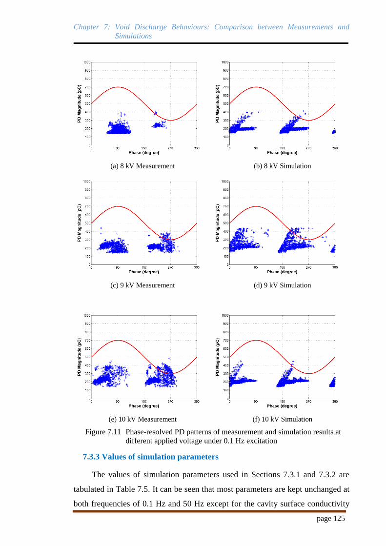
Chapter 7: Void Discharge Behaviours: Comparison between Measurements and
Simulations
page 125
(a) 8 kV Measurement (b) 8 kV Simulation
(c) 9 kV Measurement (d) 9 kV Simulation
(e) 10 kV Measurement (f) 10 kV Simulation
Figure 7.11 Phase-resolved PD patterns of measurement and simulation results at
different applied voltage under 0.1 Hz excitation
7.3.3 Values of simulation parameters
The values of simulation parameters used in Sections 7.3.1 and 7.3.2 are
tabulated in Table 7.5. It can be seen that most parameters are kept unchanged at
both frequencies of 0.1 Hz and 50 Hz except for the cavity surface conductivity

Chapter 7: Void Discharge Behaviours: Comparison between Measurements and
Simulations
page 126
value. It has been shown in previous research such as [74] and [96] that value of
cavity surface conductivity is dependent on applied frequency. Higher applied
frequency leads to rapid changes of electric field in the cavity, which stimulates
the surface charge mobility on cavity walls. Hence, surface charge decay via a
conduction mechanism on the cavity wall may be more significant.
Consequently, the enhancement of the electric field in the cavity is less
substantial and discharges are incepted with lower maximum magnitude. After
trial and error, void surface conductivity values of 1x10⁻⁹ S/m and 1x10-11 S/m
were chosen for 50 Hz and very low frequency simulation to keep the PD
maximum magnitude and repetition rate a close match with the measured data.
Table 7.3 Measurement results at 0.1 Hz under different applied voltages
Applied voltage (kV) 8 9 10
Maximum PD magnitude (pC) 411 439 480
Average PD magnitude (pC) 183 222 245
Minimum PD magnitude (pC) 146 144 144
Repetition rate (ppc) 1.1 2.2 2.4
Table 7.4 Simulation results at 0.1 Hz under different applied voltages
Applied voltage (kV) 8 9 10
Maximum PD magnitude (pC) 415 440 481
Average PD magnitude (pC) 197 201 207
Minimum PD magnitude (pC) 146 144 144
Repetition rate (ppc) 2.7 3.3 3.8
The electric field inception field is calculated from equation (2.7), and is
assumed independent of applied frequency and voltage. The extinction field is
determined based on the minimum discharge magnitude obtained from
measurements. It is also assumed to be constant as measured data shows that
minimum discharge magnitude is independent of applied voltage and frequency
excitation.
Once the parameters for the inception field, extinction field and cavity
surface conductivity have been determined, the three freely adjustable

Chapter 7: Void Discharge Behaviours: Comparison between Measurements and
Simulations
page 127
parameters, i.e. N, decay and Nev, are chosen via a trial and error method to yield
minimum errors between the simulation and measurement results at all applied
voltages and frequencies. Values of these parameters, shown in Table 7.6, were
obtained after many simulation trials. These values are not the real physical
parameters. However, their values are physically sensible to describe what
happens in the cavity. From simulation parameters, values of N and Nev are
smaller at lower frequency. They are physically sensible as the time span
between PD events is much longer at very low frequency, causing more surface
charges to disappear via several charge decay mechanisms such as charge
recombination and drifting into deeper traps in the bulk insulation. As a result,
the electron generation rate is reduced significantly and there are fewer free
charges ready for the next PD event.
Table 7.5 Simulation parameters
Parameters 0.1 Hz 50 Hz Unit
Applied voltage, Urms 8, 9, 10 kV
Number of simulation cycles, n 500
Time step during no PD, t 1/500f s
Time step during PD, dt 1x10⁻⁹ s
Relative permittivity of insulation, r 3.5
Cavity surface relative permittivity, r 3.5
Cavity relative permittivity, cav 1
Cavity conductivity during no PD, cavL 0 S/m
Cavity conductivity during PD, cavH 5x10⁻³ S/m
Electric inception field, Einc 3.93x10⁶ V/m
Electric extinction field, Eext 1x10⁶ V/m
Cavity surface low conductivity, sL 0 S/m
Cavity surface high conductivity, sH 1x10-11 1x10⁻⁹ S/m
7.3.4 Simulation for 10 applied voltage cycles
Figure 7.12 to Figure 7.14 shows the simulated electric field and PD
magnitude behaviours, cycle to cycle, under different applied voltages at 0.1 Hz
for 10 successive cycles. In general, there are more PD events and larger PD
magnitude at higher applied voltage as observed in the measurement results. The
simulation shows a PD event with larger magnitude is incepted at a higher cavity
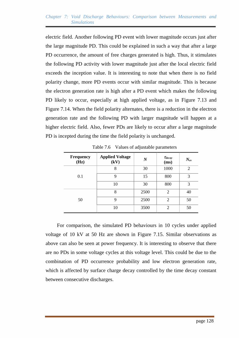
Chapter 7: Void Discharge Behaviours: Comparison between Measurements and
Simulations
page 128
electric field. Another following PD event with lower magnitude occurs just after
the large magnitude PD. This could be explained in such a way that after a large
PD occurrence, the amount of free charges generated is high. Thus, it stimulates
the following PD activity with lower magnitude just after the local electric field
exceeds the inception value. It is interesting to note that when there is no field
polarity change, more PD events occur with similar magnitude. This is because
the electron generation rate is high after a PD event which makes the following
PD likely to occur, especially at high applied voltage, as in Figure 7.13 and
Figure 7.14. When the field polarity alternates, there is a reduction in the electron
generation rate and the following PD with larger magnitude will happen at a
higher electric field. Also, fewer PDs are likely to occur after a large magnitude
PD is incepted during the time the field polarity is unchanged.
Table 7.6 Values of adjustable parameters
Frequency
(Hz)
Applied Voltage
(kV) N
decay
(ms) Nev
0.1
8 30 1000 2
9 15 800 3
10 30 800 3
50
8 2500 2 40
9 2500 2 50
10 3500 2 50
For comparison, the simulated PD behaviours in 10 cycles under applied
voltage of 10 kV at 50 Hz are shown in Figure 7.15. Similar observations as
above can also be seen at power frequency. It is interesting to observe that there
are no PDs in some voltage cycles at this voltage level. This could be due to the
combination of PD occurrence probability and low electron generation rate,
which is affected by surface charge decay controlled by the time decay constant
between consecutive discharges.

Chapter 7: Void Discharge Behaviours: Comparison between Measurements and
Simulations
page 129
(a) Electric field simulation
(b) Discharge magnitudes
Figure 7.12 Simulation of electric field and PD magnitude for 10 cycles at 0.1 Hz
under applied voltage of 8 kV
(a) Electric field simulation
(b) Discharge magnitudes
Figure 7.13 Simulation of electric field and PD magnitude for 10 cycles at 0.1 Hz
under applied voltage of 9 kV
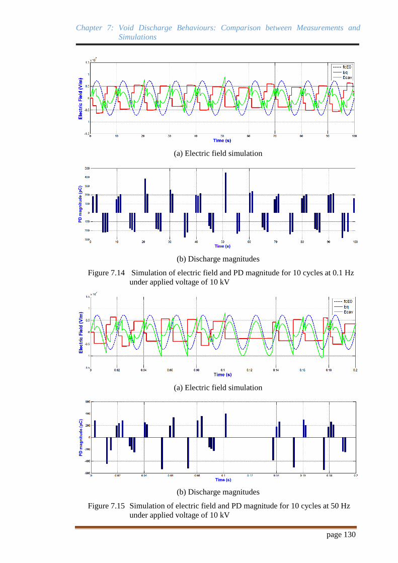
Chapter 7: Void Discharge Behaviours: Comparison between Measurements and
Simulations
page 130
(a) Electric field simulation
(b) Discharge magnitudes
Figure 7.14 Simulation of electric field and PD magnitude for 10 cycles at 0.1 Hz
under applied voltage of 10 kV
(a) Electric field simulation
(b) Discharge magnitudes
Figure 7.15 Simulation of electric field and PD magnitude for 10 cycles at 50 Hz
under applied voltage of 10 kV

Chapter 7: Void Discharge Behaviours: Comparison between Measurements and
Simulations
page 131
7.4 Calculation of statistical time lag of partial discharge events
As described in Chapter 2, the statistical time lag is the average time span
between the moment the inception field is exceeded and the moment the
discharge actually occurs. With the help of simulation of the proposed partial
discharge model, this value could be determined for every single PD event.
Figure 7.16 shows the simulation of the electric field in a cavity in time and how
the statistical time lag is calculated. It is determined from the time when the local
field, Ecav, exceeds the inception value, Einc, to the time the following PD
happens. The average value of this time constant is equal to the sum of each time
lag divided by the total number of PD events.
stat stat stat
tn tn tn
Figure 7.16 Calculation of statistical time lag of PD events
Figure 7.17 shows the distribution of statistical time lag under different
applied voltage at 0.1 Hz and 50 Hz for 500 simulation cycles as described in
Section 7.3. The average time lag values are tabulated in Table 7.7. At both
frequencies, the average statistical time lag is lower with higher applied voltage.
This is expected as higher amplitude of the applied field increases the electron
generation rate, which reduces relatively the average waiting time for available
electrons to ignite a PD event when the inception field is exceeded. It is also
confirmed by the parameter value of the number of electrons generated at
inception field Einc, i.e. N, which is larger at higher simulated applied voltage at
both frequencies.
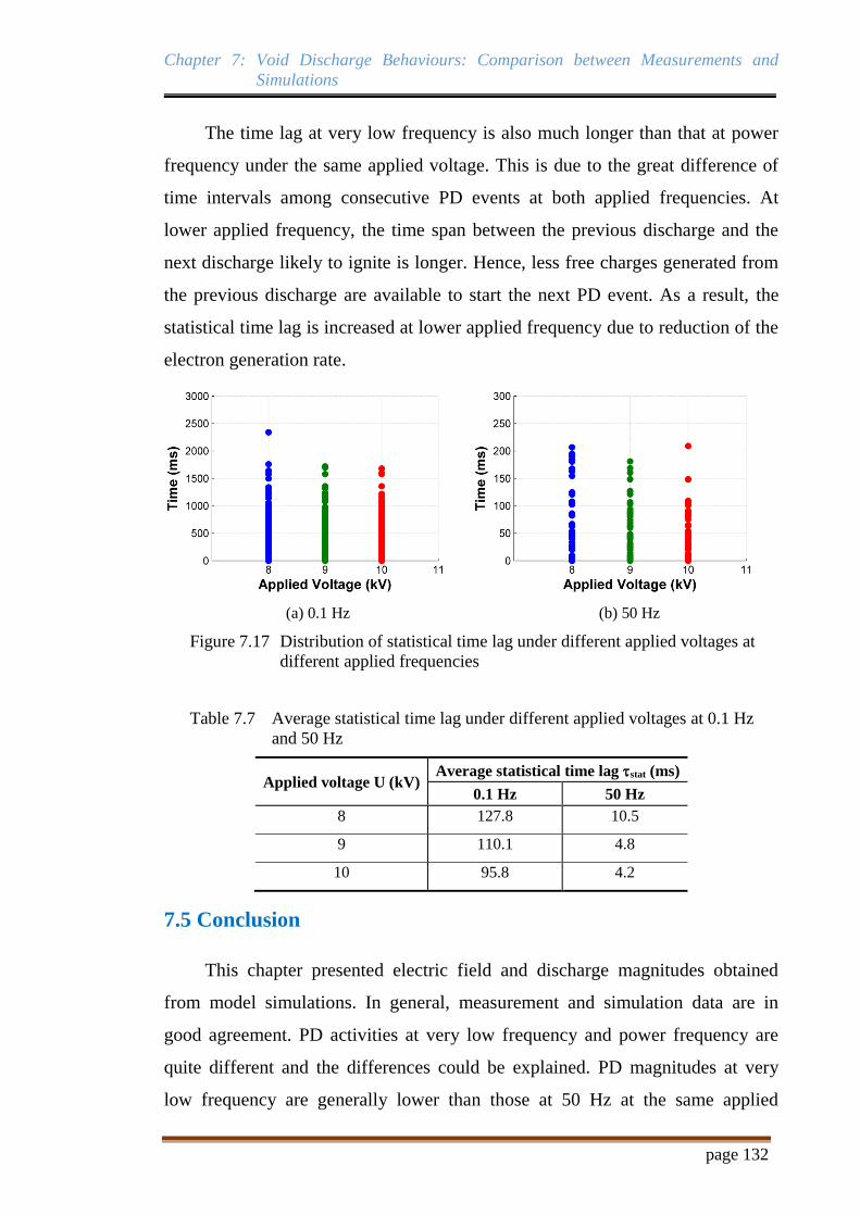
Chapter 7: Void Discharge Behaviours: Comparison between Measurements and
Simulations
page 132
The time lag at very low frequency is also much longer than that at power
frequency under the same applied voltage. This is due to the great difference of
time intervals among consecutive PD events at both applied frequencies. At
lower applied frequency, the time span between the previous discharge and the
next discharge likely to ignite is longer. Hence, less free charges generated from
the previous discharge are available to start the next PD event. As a result, the
statistical time lag is increased at lower applied frequency due to reduction of the
electron generation rate.
(a) 0.1 Hz (b) 50 Hz
Figure 7.17 Distribution of statistical time lag under different applied voltages at
different applied frequencies
Table 7.7 Average statistical time lag under different applied voltages at 0.1 Hz
and 50 Hz
Applied voltage U (kV) Average statistical time lag stat (ms)
0.1 Hz 50 Hz
8 127.8 10.5
9 110.1 4.8
10 95.8 4.2
7.5 Conclusion
This chapter presented electric field and discharge magnitudes obtained
from model simulations. In general, measurement and simulation data are in
good agreement. PD activities at very low frequency and power frequency are
quite different and the differences could be explained. PD magnitudes at very
low frequency are generally lower than those at 50 Hz at the same applied
Chapter 7: Void Discharge Behaviours: Comparison between Measurements and
Simulations
page 133
voltage. The number of discharges per cycle is higher at larger applied voltage at
both frequencies. From simulation, they could be due to the dependence of the
electron generation rate on applied voltage and frequency. It has been confirmed
that free electrons generated from surface emission and volume ionisation are
larger at higher frequency although their values are not the actual physical
parameters. The surface charge decay also contributes significantly to the
difference of partial discharge activities at both frequencies. At higher applied
frequency, cavity surface conductivity is larger which results in more
accumulated charges decay because charge movement along the cavity wall is
faster due to the shorter period of applied voltage. However, the effect of surface
charge decay is reduced at higher applied frequency as the time span between
consecutive discharges is much shorter. Hence, the statistical time lags are much
shorter at higher frequency and more discharges are incepted almost immediately
after the inception field is exceeded.
By comparing measurement and simulation results, critical parameters
influencing partial discharge activities at different applied voltage and frequency
can be determined including the inception field, extinction field, cavity surface
conductivity and effective charge decay time constant. Physical mechanisms
involved in partial discharge activities are the electron generation rate via surface
emission and volume ionisation and charge decay through charge trapping,
charge conduction along the cavity wall and charge recombination. The
following chapter summarises and concludes the research.
page 134
Chapter 8: Conclusion and Future
Work
8.1 Conclusion
This thesis developed and reported extensive empirical work to investigate
partial discharge under different stress conditions at very low frequency and
power frequency. The measurements have been done with two types of partial
discharge: corona discharge and internal discharge in a cavity. For corona
discharge, the test object was stressed under different applied waveforms such as
sine wave, square wave and sine wave with DC offset. The effects of ambient
temperatures on corona discharge were also investigated at very low frequency
and power frequency under excitation of sine wave and sine wave with DC
offset. Measurements of internal discharge in a cylindrical cavity have been
undertaken extensively at both frequencies of 0.1 Hz and 50 Hz as a function of
cavity size and applied voltage waveforms including sinusoidal and trapezoid-
based voltages. In order to determine critical parameters affecting internal
discharge behaviours, a discharge model has been developed and verified with
measurement results. The comparison between measurement and simulation
results revealed that physical parameters in the cavity are strongly dependent on
the applied frequency. A summary of experimental, analytical and simulation
studies of partial discharge characteristics in this thesis, together with main
findings drawn from the work, is presented below.
Chapter 1 presented the motivation of this research and explained the
importance of partial discharge diagnostic tests at very low frequency excitation.
Literature on partial discharge was reviewed in Chapter 2, including several
partial discharge models which have been developed using analytical and
dynamic approaches to simulate the internal discharge in a cavity. Critical
parameters affecting discharge activities identified from the simulation included

Chapter 8: Conclusion and Future Work
page 135
the initial electron generation rate, charge decay time constant, statistical time lag
and inception field. However, the analytical models were only applied for
investigation at power frequency. Of the dynamic models, one proposed model
was used to simulate partial discharge in the frequency range of 0.01 Hz to 100
Hz but it did not take into account the charge decay phenomenon. Another
proposed dynamic model did consider the charge decay phenomenon but it was
assumed that the charge decay time constant is fixed over the frequency range
studied (1 Hz to 50 Hz). This model was not verified at very low frequency.
Therefore, the discharge model developed and presented in this thesis aims
to include the charge decay phenomenon with frequency-dependent values for
the charge decay time constant. The proposed discharge model to simulate
internal discharge dynamically was described in detail in Chapter 3. The model
has a minimal set of adjustable parameters which allows it to simulate the
discharge behaviours at different frequencies in a reasonable period of time. This
advantage made it possible to investigate partial discharge under various stress
conditions such as voltage amplitudes and applied frequencies. The surface
charge distribution and its effects on subsequent partial discharges were also
obtained using this proposed model.
In order to investigate the partial discharge, an important task is to conduct
experiments and gather raw discharge data. The conventional partial discharge
measurement system fully compliant to the IEC 60270 standard was used to
record the partial discharge characteristics. The equipment setup was described in
Chapter 4. The partial discharge analysis, calculation of discharge parameters
and phase-resolved partial discharge pattern technique were also presented. Two
types of discharges, corona discharge and internal discharge, were generated in
the laboratory by preparing the appropriate test objects. A needle and bowl
electrode configuration was used to produce corona discharge. Internal discharge
was generated in a cylindrical cavity embedded in a solid dielectric test sample
which was fabricated by using a 3D printer. The experiment procedures were
described extensively to ensure the consistency of recorded partial discharge data
at different applied stress conditions.
Chapter 8: Conclusion and Future Work
page 136
Chapter 5 presented experimental results of corona discharge at very low
frequency and power frequency. It was found that the applied voltage waveform
affects the inception voltage of corona discharge at very low frequency.
Inception voltage, in the case of applied square wave and sine wave with DC
offset, was found to be lower than that under the pure sine wave. This is likely to
be explained by the longer duration of high negative voltage amplitude applied to
the needle under the square wave and sine wave with DC offset. The high level
of negative voltage amplitude causes the negative corona discharge to be
triggered more easily. The experiment results supported a hypothesis that a faster
rise time of voltage results in larger discharge repetition rate and discharge
magnitudes.
The effects of ambient temperatures on corona discharge were also
investigated at both frequencies of 0.1 Hz and 50 Hz. It was shown that discharge
characteristics under both frequencies had similar behaviours in such a way that
higher ambient temperature caused discharges to occur with larger magnitudes
and earlier regarding the voltage phase. This was due to the increase of free
electron availability injected from the needle at higher temperatures.
Chapter 6 described one of the main contributions of this thesis. A
comparative experimental study of cavity discharges was presented as a function
of cavity size and applied voltage waveforms at frequencies of 0.1 Hz and 50 Hz.
Changes of discharge characteristics after long discharge exposure were obtained
at various applied frequencies. This could be due to the differences of cavity
surface conductivity evolution during the exposed discharge period. Cavity
discharge characteristics were found to be strongly dependent on applied voltage
waveforms and the rate of voltage rise. Discharge magnitudes were generally
smaller at lower applied frequency regardless of applied voltage waveforms. It
was found that more discharges with low magnitudes occurred in a larger cavity
as the effective discharge area was increased. These findings could be explained
by the dependence of surface charge decay on applied frequency. The surface
charge decay was likely to be more significant at lower applied frequency.
Chapter 8: Conclusion and Future Work
page 137
The simulation results presented in Chapter 7 confirmed the effects of
charge decay on cavity discharge characteristics. The simulated value of cavity
surface conductivity, which was verified by measurement results, increased at
higher applied frequency and thus there was more surface charge decay in time
despite it not being the actual physical value. However, the charge decay rate was
reduced at frequency of 50 Hz since the time span between consecutive
discharges was much shorter.
The effect of charge decay also contributed to differences in partial
discharge behaviours at different applied frequencies. Discharge magnitudes at
very low frequency were found to be lower than those at power frequency at the
same voltage amplitude. The discharge repetition rate was also lower at lower
applied frequency. These differences were attributed to the dependence of the
adjustable parameters in the simulation model on applied frequency. It was
verified that the amont of free electrons generated from surface emission and
volume ionisation was smaller at lower frequency while the charge decay time
constant was shorter at higher frequency. From simulation, the effects of charge
distribution on the cavity surface on subsequent discharges were analysed at both
very low frequency and power frequency. The statistical time lag of every single
discharge was calculated numerically to illustrate the dependence of discharge
behaviours on applied frequency.
In summary, this thesis presents extensive empirical work investigating
partial discharge at very low frequency and power frequency under different
stress conditions. The phase-resolved partial discharge patterns obtained from
simulations and measurements were analysed thoroughly to explore the discharge
differences. The explanation of these differences was discussed analytically and
confirmed via a simulation approach.
For corona discharges, it was found that maximum and average discharge
magnitudes at 50 Hz were larger than those at 0.1 Hz under the same applied
voltage amplitude. Although the repetition rate of corona discharge at 0.1 Hz was
larger than that at 50 Hz in terms of pulses per cycle, it was lower at 0.1 Hz than

Chapter 8: Conclusion and Future Work
page 138
at 50 Hz in terms of pulses per second. The obtained phase-resolved patterns
were fairly similar at both applied frequencies.
For internal discharge, discharge behaviours were found to be dependent on
applied voltage waveforms. Under the sinusoidal voltage excitation, maximum
and average discharge magnitudes at 50 Hz were generally larger than those at
0.1 Hz under the same voltage amplitude. The repetition rate of discharges at 50
Hz was also larger than that at 0.1 Hz in terms of both pulses per second and
pulses per cycle. The obtained phase-resolved patterns were quite different under
different applied frequencies. The discharge patterns at 50 Hz had the “rabbit-
ear” shape which was formed by large discharges occurring early in voltage
phase. On the contrary, this distinct shape was hardly observed at 0.1 Hz since
most large discharges occurred later in voltage phase.
Under square voltage excitation, maximum and average discharge
magnitudes at 0.1 Hz were much lower than those at 50 Hz under the same
applied voltage. Although the repetition rate of discharges at 0.1 Hz was smaller
than that at 50 Hz at different voltage amplitudes in terms of pulses per second, it
was higher at 0.1 Hz than at 50 Hz in terms of pulses per cycle. The obtained
phase-resolved patterns at both frequencies were clearly different. Discharge
occurrence at 0.1 Hz was concentrated in the duration of voltage polarity
reversal. Discharges were barely detected during the period of constant voltage.
On the contrary, the majority of discharges occurred at the voltage changing
period under 50 Hz excitation. There were a number of discharges with low
magnitudes observed during the “flat” peak voltage of square waveform.
Under triangular voltage excitation, maximum discharge magnitude at 50
Hz was generally larger than that at 0.1 Hz even at lower applied voltage
amplitude. Average discharge magnitude at 50 Hz was larger as compared to 0.1
Hz at the same applied voltage. The repetition rate of discharges at 50 Hz was
larger than that at 0.1 Hz even at lower applied voltage in terms of both pulses
per second and pulses per cycle. The obtained phase-resolved patterns were quite
different. Discharge distribution at 50 Hz was mainly in the front voltage rise. On
Chapter 8: Conclusion and Future Work
page 139
the contrary, discharge distribution at 0.1 Hz was mainly around the peak voltage
regions with large discharges occurring at later voltage phase.
Under trapezoidal voltage excitation, maximum and average discharge
magnitudes at 0.1 Hz were generally lower than those at 50 Hz even at higher
applied voltage amplitudes. The repetition rate of discharges at 0.1 Hz was
smaller than that at 50 Hz even at higher applied voltage in terms of both pulses
per second and pulses per cycle. The obtained phase-resolved patterns were quite
similar. Most of detected discharges occurred during the voltage polarity reversal
period. There were a few discharges with low magnitudes occurred during the
constant voltage period at both applied frequencies.
8.2 Future research directions
The partial discharge model with a minimal set of adjustable parameters
proposed in the thesis successfully simulates discharge activities in a cylindrical
cavity at very low frequency of 0.1 Hz and power frequency of 50 Hz. Although
the measurement and simulation results show good agreement, there are still
some differences. These discrepancies might be due to the measurements or the
simulations. For instance, the measured discharge data might not be recorded
accurately due to switching interferences from the very low frequency test supply
(high voltage amplifier) or other testing activities in the laboratory.
There might be errors in simulated partial discharge results due to several
assumptions made to simplify the model. The differences might also be caused
by estimation of the model adjustable parameters due to the time-consuming trial
and error procedures. Therefore, the discharge model can be improved with
further work. Also, it should take into account other factors such as temperature
and pressure in the cavity whilst retaining the minimal number of adjustable
parameters if possible. By adopting state-of-the-art optimisation algorithms, it
should be more efficient and the simulation time to search for the best parameter
values can be reduced.
The simulation work of this thesis only used sinusoidal voltage at frequency
of 0.1 Hz and 50 Hz although the measured discharge data under other applied
Chapter 8: Conclusion and Future Work
page 140
voltage waveforms are available. Thus, this study should be extended in
simulating cavity discharges under other applied waveforms such as triangular,
trapezoid-based and customised wave. This will enable a broader understanding
of discharge behaviours across multiple voltage waveforms.
With the capability of the arbitrary function generator, voltage waveforms
with a wide range of frequencies can be generated. As a result, future research on
partial discharge should be conducted at more values of applied frequencies. This
will provide extensive discharge results across a wide frequency range of applied
voltage to give an in-depth analysis of discharge characteristics. These measured
results can be used to verify the simulation under the same conditions to exploit
more valuable information on discharge behaviours over a broad range of
frequencies.
The cavity discharge study in this thesis was restricted to a cylindrical void
in Acrylonitrile-Butadiene-Styrene (ABS) material. Although ABS material is
not widely used for high voltage insulation, this research successfully
demonstrates the cavity discharge behaviours in a plastic material at very low
frequency and power frequency. A similar methodology can be used in future
partial discharge research on various cavity geometries with different types of
insulation materials. Of course, this will depend on the ability of 3D printing
technology to work with such materials.
Despite the different physical mechanisms between cavity discharge and
corona discharge, corona discharge can be simulated dynamically by using a
similar approach. A corona discharge model can be developed to investigate the
effects of various insulating media on corona discharge activities.
Another ambient condition affecting the corona discharge which was not
considered in this research is humidity. As high voltage equipment is usually
operated under varying humidity levels, it is essential to investigate the effects of
humidity on corona discharge at very low frequency.
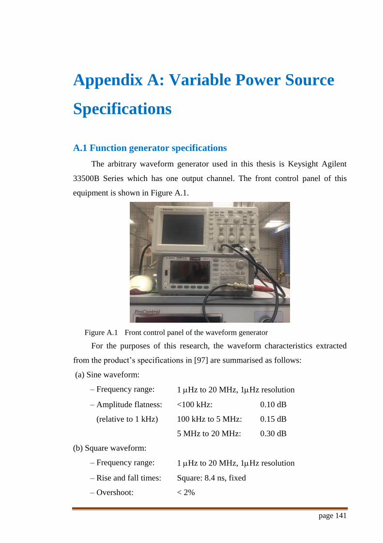
page 141
Appendix A: Variable Power Source
Specifications
A.1 Function generator specifications
The arbitrary waveform generator used in this thesis is Keysight Agilent
33500B Series which has one output channel. The front control panel of this
equipment is shown in Figure A.1.
Figure A.1 Front control panel of the waveform generator
For the purposes of this research, the waveform characteristics extracted
from the product’s specifications in [97] are summarised as follows:
(a) Sine waveform:
– Frequency range: 1 Hz to 20 MHz, 1Hz resolution
– Amplitude flatness:
(relative to 1 kHz)
<100 kHz:
100 kHz to 5 MHz:
5 MHz to 20 MHz:
0.10 dB
0.15 dB
0.30 dB
(b) Square waveform:
– Frequency range: 1 Hz to 20 MHz, 1Hz resolution
– Rise and fall times: Square: 8.4 ns, fixed
– Overshoot: < 2%

page 142
– Duty cycle: 0.01% to 99.99%
– Pulse width: 16 ns minimum
(c) Triangle and ramp waveform:
– Frequency range: 1 Hz to 20 kHz, 1Hz resolution
– Ramp symmetry: 0.0% to 100.0 %, 0.1% resolution
(0% is negative ramp, 100% is positive ramp,
50% is triangle)
– Nonlinearity: < 0.05% from 5% to 95% of the signal amplitude
(d) Arbitrary waveform:
– Waveform length: 8 Sa to 1 MSa
– Sample rate: 1 Sa/s to 250 MSa/s, 1 Sa/s resolution
– Voltage resolution: 16 bits
A.2 High voltage amplifier specifications
In this research, high voltage amplitudes at variable waveforms are
generated by using a Trek 20/20C-HS high voltage amplifier receiving the input
signal from the waveform generator. This instrument amplifies the received
signal 2000 times and generates high voltage at the output terminal. The front
control panel of this equipment with the settings used during the experiments is
shown in Figure A.2.
Figure A.2 Front control panel of high voltage amplifier
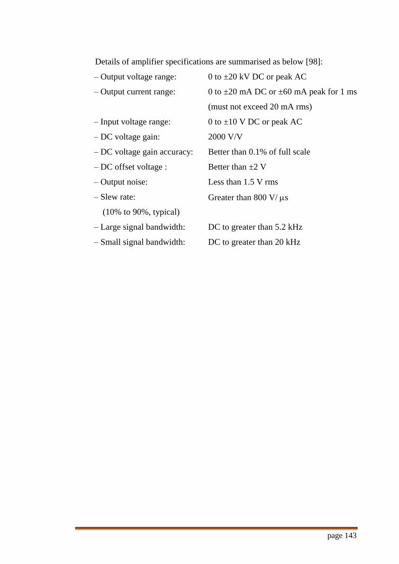
page 143
Details of amplifier specifications are summarised as below [98]:
– Output voltage range: 0 to ±20 kV DC or peak AC
– Output current range: 0 to ±20 mA DC or ±60 mA peak for 1 ms
(must not exceed 20 mA rms)
– Input voltage range: 0 to ±10 V DC or peak AC
– DC voltage gain: 2000 V/V
– DC voltage gain accuracy: Better than 0.1% of full scale
– DC offset voltage : Better than ±2 V
– Output noise: Less than 1.5 V rms
– Slew rate:
(10% to 90%, typical)
Greater than 800 V/ s
– Large signal bandwidth: DC to greater than 5.2 kHz
– Small signal bandwidth: DC to greater than 20 kHz

page 144
Appendix B: Usage of Mtronix
MPD600 Software
B.1 Graphic User Interface of Mtronix MPD600
Main sections of the general Graphic User Interface (GUI) of Mtronix
MPD600 are shown in Figure B.1. Details of these sections are as follows:
1. Acquisition unit display: Types of acquisition units detected by the
software are shown in this area.
2. Visualisation display: This area visually displays the majority of the
parameters and graphs needed by user’s interests. It occupies most of
the left half of the user interface. This section includes a large scope
view at the top left corner (4), a smaller scope view at bottom left corner
(5) and a display box of measured quantities at the centre of the
interface (6).
3. Control panel: This provides access to all functions of the software via
appropriate tabs.
4. Large scope view: This normally displays the phase-resolved pattern of
discharges during measurements.
5. Small scope view: This area can display the spectrum of input signal,
time-domain signal and trend curves of measured quantities.
6. Measured quantities display: This box displays values of measured
quantities such as apparent charges, number of recorded discharges,
recording duration and measurement bandwidth.
B.2 Calibration procedures prior to measurements
Calibration must be done prior to any measurements in this thesis. The
calibrator CAL542 is connected in parallel with the test object and injects a
known amount of charges, i.e. 50 pC, into the measurement circuit. The

page 145
measuring frequency settings are 250 kHz of centre frequency and 300 kHz of
bandwidth.
1
5
2
4
63
Figure B.1. Mtronix MPD600 Graphic User Interface
Calibration steps in Figure B.2 are as follows:
1. Under Q tab: go to Charge intergration settings, set fCenter = 250 kHz
and f = 300 kHz.
2. Under Q tab: go to Display settings, set Qmax and Qmin equal to 100 pC
and 1 pC, respectively in order to display the calibration signal of 50 pC
properly.
3. Under Q tab: go to Calibration Settings, set QIEC (target) equal to 50
pC.
4. Press Compute button to finish the calibration.
Once the calibration is done, the QIEC (measured) should display a reading
very close to 50 pC.
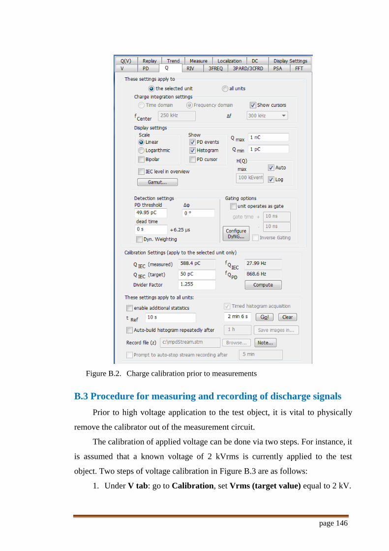
page 146
Figure B.2. Charge calibration prior to measurements
B.3 Procedure for measuring and recording of discharge signals
Prior to high voltage application to the test object, it is vital to physically
remove the calibrator out of the measurement circuit.
The calibration of applied voltage can be done via two steps. For instance, it
is assumed that a known voltage of 2 kVrms is currently applied to the test
object. Two steps of voltage calibration in Figure B.3 are as follows:
1. Under V tab: go to Calibration, set Vrms (target value) equal to 2 kV.
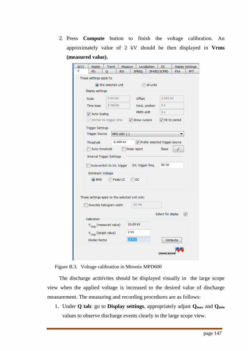
page 147
2. Press Compute button to finish the voltage calibration. An
approximately value of 2 kV should be then displayed in Vrms
(measured value).
Figure B.3. Voltage calibration in Mtronix MPD600
The discharge actitivites should be displayed visually in the large scope
view when the applied voltage is increased to the desired value of discharge
measurement. The measuring and recording procedures are as follows:
1. Under Q tab: go to Display settings, appropriately adjust Qmax and Qmin
values to observe discharge events clearly in the large scope view.

page 148
2. To view the discharge histogram for a specific time length, check the
Time histogram acquisition box under the Q tab and set the desired time
length. Then, press Go! Button as in Figure B.2.
3. To record discharge activities, firstly specify the file name and its location
in the Record file(z) under the Q tab. To start recording, press the
Record button. To finish recording, press the Record button again.
Figure B.4 shows an example of recorded time histogram plot of
discharges.
Figure B.4. An example of time histogram of discharges
B.4 Procedures of exporting recorded data to MATLAB
compatible files
Procedures of exporting recorded data in Figure B.5 for further analysis are
as follows:
1. Open the desired recorded file with filename extension .stm. A Replay
tab should be displayed in the Control Panel area.
2. Under Replay tab: go to Replay range and set desirable time length in
Start replay at and replay for boxes.
3. Under the Replay tab: go to Export to Matlab and specify the location
of exported data. Then, check the boxes of Export Matlab-compatible
files and generate phase vector file before pressing the play button.
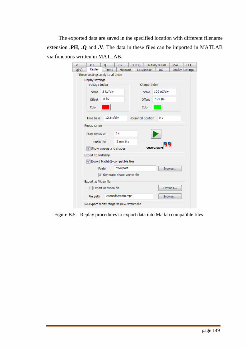
page 149
The exported data are saved in the specified location with different filename
extension .PH, .Q and .V. The data in these files can be imported in MATLAB
via functions written in MATLAB.
Figure B.5. Replay procedures to export data into Matlab compatible files
page 150
References
[1] E. Gulski et al., “On-site testing and PD diagnosis of high voltage power cables,” IEEE
Trans. Dielectr. Electr. Insul., vol. 15, no. 6, pp. 1691–1700, Dec. 2008.
[2] U. Schichler, H. Borsi, and E. Gockenbach, “On-site cable testing with a resonant test set
and an additional partial discharge measurement,” in Conference Record of the 1996
IEEE International Symposium on Electrical Insulation, 1996, vol. 1, pp. 138–141.
[3] P. Mohaupt, M. Baur, and T. Schlick, “VLF testing and diagnosis on medium voltage
power cables,” in 2003 IEEE 10th International Conference on Transmission and
Distribution Construction, Operation and Live-Line Maintenance, 2003, pp. 202–209.
[4] H. T. Putter, D. Gotz, F. Petzold, and H. Oetjen, “The evolution of VLF testing
technologies over the past two decades,” in 2012 IEEE PES Transmission and
Distribution Conference and Exposition, 2012, pp. 1–4.
[5] H. Oetjen, “Principals and field experience with the 0.1 Hz VLF method regarding the
test of medium voltage distribution cables,” in Conference Record of the 2004 IEEE
International Symposium on Electrical Insulation, 2004, pp. 376–379.
[6] H. R. Gnerlich, “Field testing of HV power cables: understanding VLF testing,” IEEE
Electr. Insul. Mag., vol. 11, no. 5, pp. 13–16, Sep. 1995.
[7] M. T. Peschel, “Needed changes in medium voltage cable testing. Were you in on it?
Welcome to the world of VLF.,” in 2010 IEEE International Symposium on Electrical
Insulation, 2010, pp. 1–5.
[8] G. S. Eager, C. Katz, B. Fryszczyn, J. Densley, and B. S. Bernstein, “High voltage VLF
testing of power cables,” IEEE Trans. Power Deliv., vol. 12, no. 2, pp. 565–570, Apr.
1997.
[9] IEEE Guide for Field Testing of Shielded Power Cable Systems Using Very Low
Frequency (VLF)(less than 1 Hz), IEEE 400.2 Standard, 2013.
[10] IEC 60270 International Standard: High-voltage test techniques – Partial discharge
measurements, IEC 60270 Standard, 2000.
[11] T. Tanaka, “Internal Partial Discharge and Material Degradation,” IEEE Trans. Electr.
Insul., vol. EI-21, no. 6, pp. 899–905, Dec. 1986.
[12] D. A. Seanor, Electrical Properties of Polymers. London, U.K.: Academic Press Inc.,
1982.
[13] V. Krotov and A. Cavallini, “Comparison of PD patterns at power and very low
frequency: Is diagnostic possible?,” in 2013 IEEE International Conference on Solid
Dielectrics (ICSD), 2013, pp. 109–112.
page 151
[14] W. Hauschild, A. Cavallini, and G. C. C. Montanari, “Effect of supply voltage frequency
on testing of insulation system,” IEEE Trans. Dielectr. Electr. Insul., vol. 13, no. 1, pp.
111–121, Feb. 2006.
[15] K. Rethmeier and R. Blank, “Partial discharge measurements in the sub-VLF range,” in
9th International Conference on Insulated Power Cables, 2015, pp. 1–6.
[16] R. Miller and I. Black, “Partial discharge measurements over the frequency range 0.1 Hz
to 50 Hz,” IEEE Trans. Electr. Insul., vol. EI-12, no. 3, pp. 224–233, Jun. 1977.
[17] R. Bodega, A. Cavallini, P. H. F. Morshuis, and F. J. Wester, “The effect of voltage
frequency on partial discharge activity,” in Annual Report Conference on Electrical
Insulation and Dielectric Phenomena, 2002, pp. 685–689.
[18] R. Bodega, P. H. F. Morshuis, M. Lazzaroni, and F. J. Wester, “PD recurrence in
cavisties at different energizing methods,” IEEE Trans. Instrum. Meas., vol. 53, no. 2,
pp. 251–258, Apr. 2004.
[19] A. Cavallini and G. C. Montanari, “Effect of supply voltage frequency on testing of
insulation system,” IEEE Trans. Dielectr. Electr. Insul., vol. 13, no. 1, pp. 111–121, Feb.
2006.
[20] A. Cavallini, V. Krotov, G. C. Montanari, P. H. F. Morshuis, and L. E. Mariut, “The role
of supply frequency in the evaluation of partial discharge inception voltage in XLPE-
embedded cavities,” in 2012 Annual Report Conference on Electrical Insulation and
Dielectric Phenomena (CEIDP), 2012, pp. 487–490.
[21] A. Cavallini, G. C. Montanari, and L. E. Mariut, “The influence of test voltage
waveforms on partial discharge activity in XLPE,” in 2012 IEEE International
Symposium on Electrical Insulation, 2012, pp. 554–557.
[22] C. Forssen and H. Edin, “Partial discharges in a cavity at variable applied frequency part
1: measurements,” IEEE Trans. Dielectr. Electr. Insul., vol. 15, no. 6, pp. 1601–1609,
Dec. 2008.
[23] T. Okamoto, T. Kato, Y. Yokomizu, Y. Suzuoki, and T. Tanaka, “PD characteristics as a
stochastic process and its integral equation under sinusoidal voltage,” IEEE Trans.
Dielectr. Electr. Insul., vol. 8, no. 1, pp. 82–90, 2001.
[24] N. Hozumi, H. Nagae, Y. Muramoto, M. Nagao, and H. Xie, “Time-lag measurement of
void discharges and numerical simulation for clarification of the factor for partial
discharge pattern,” in Proceedings of 2001 International Symposium on Electrical
Insulating Materials (ISEIM 2001), 2001, pp. 29–32.
[25] M. Hikita, K. Yamada, A. Nakamura, T. Mizutani, A. Oohasi, and M. Ieda,
“Measurements of partial discharges by computer and analysis of partial discharge
distribution by the Monte Carlo method,” IEEE Trans. Electr. Insul., vol. 25, no. 3, pp.
453–468, Jun. 1990.

page 152
[26] H. Suzuki, K. Aihara, and T. Okamoto, “Complex behaviour of a simple partial-
discharge model,” Europhys. Lett., vol. 66, no. 1, pp. 28–34, Apr. 2004.
[27] A. Pedersen, G. C. Crichton, and I. W. McAllister, “The theory and measurement of
partial discharge transients,” IEEE Trans. Electr. Insul., vol. 26, no. 3, pp. 487–497, Jun.
1991.
[28] G. C. Crichton, P. W. Karlsson, and A. Pedersen, “Partial discharges in ellipsoidal and
spheroidal voids,” IEEE Trans. Electr. Insul., vol. 24, no. 2, pp. 335–342, Apr. 1989.
[29] A. Pedersen, “Partial discharges in voids in solid dielectrics. An alternative approach,” in
Conference on Electrical Insulation & Dielectric Phenomena — Annual Report 1987,
1987, pp. 58–64.
[30] A. Pedersen, G. C. Crichton, and I. W. McAllister, “The functional relation between
partial discharges and induced charge,” IEEE Trans. Dielectr. Electr. Insul., vol. 2, no. 4,
pp. 535–543, 1995.
[31] L. Niemeyer, “A generalized approach to partial discharge modeling,” IEEE Trans.
Dielectr. Electr. Insul., vol. 2, no. 4, pp. 510–528, 1995.
[32] F. Gutfleisch and L. Niemeyer, “Measurement and simulation of PD in epoxy voids,”
IEEE Trans. Dielectr. Electr. Insul., vol. 2, no. 5, pp. 729–743, 1995.
[33] C. Forssen and H. Edin, “Partial discharges in a cavity at variable applied frequency part
2: measurements and modeling,” IEEE Trans. Dielectr. Electr. Insul., vol. 15, no. 6, pp.
1610–1616, 2008.
[34] H. A. Illias, G. Chen, and P. L. Lewin, “Partial discharge modelling in a spherical cavity
within a dielectric insulation material as a function of frequency,” in 2009 IEEE
Electrical Insulation Conference, 2009, pp. 55–59.
[35] H. A. Illias, “Measurement and simulation of partial discharges within a spherical cavity
in a solid dielectric material,” Ph.D. thesis, University of Southampton, Southampton,
U.K, 2011.
[36] J. Kuffel, E. Kuffel, and W. S. Zaengl, High Voltage Engineering Fundamentals, 2nd
Ed., Burlington, MA, USA: Newnes (Butterworth-Heinemann), 2000.
[37] F. H. Kreuger, Industrial High Voltage: Electric Fields, Dielectrics, Constructions,
Delft, The Netherlands: Delft University Press, 1991.
[38] J. S. Townsend, Electricity in Gases. Oxford, U.K.: Clarendon Press, 1915.
[39] B. T. Phung, “Computer-based partial discharge detection and characterisation,” Ph.D.
thesis, Deparment of Electric Power Engineering, University of New South Wales,
Sydney, Australia, 1997.
[40] G. W. Trichel, “The Mechanism of the Positive Point-to-Plane Corona in Air at
Atmospheric Pressure,” Phys. Rev., vol. 55, no. 4, pp. 382–390, Feb. 1939.
[41] F. H. Kreuger, Partial Discharge Detection in High-Voltage Equipment, London, U.K.:

page 153
Butterworths, 1989.
[42] S. A. Boggs, “Partial discharge. III. Cavity-induced PD in solid dielectrics,” IEEE
Electr. Insul. Mag., vol. 6, no. 6, pp. 11–16, Nov. 1990.
[43] S. Boggs and J. Densley, “Fundamentals of partial discharge in the context of field cable
testing,” IEEE Electr. Insul. Mag., vol. 16, no. 5, pp. 13–18, Sep. 2000.
[44] G. C. Montanari, “On line partial discharge diagnosis of power cables,” in 2009 IEEE
Electrical Insulation Conference, 2009, pp. 210–215.
[45] S. J. Sutton, J. V. Champion, S. G. Swingler, Y. Zhao, A. S. Vaughan, and S. J. Dodd,
“Influence of morphology on electrical treeing in polyethylene blends,” IEE Proc. - Sci.
Meas. Technol., vol. 150, no. 2, pp. 58–64, Mar. 2003.
[46] P. H. F. Morshuis, “Degradation of solid dielectrics due to internal partial discharge:
some thoughts on progress made and where to go now,” IEEE Trans. Dielectr. Electr.
Insul., vol. 12, no. 5, pp. 905–913, Oct. 2005.
[47] Z. Achillides, G. Georghiou, and E. Kyriakides, “Partial discharges and associated
transients: the induced charge concept versus capacitive modeling,” IEEE Trans.
Dielectr. Electr. Insul., vol. 15, no. 6, pp. 1507–1516, Dec. 2008.
[48] A. Alsheikhly, H. Guzman, and H.-G. Kranz, “A new diagnostic tool through computer
simulation calculation using expanded partial discharge equivalent circuit,” in
Proceedings of the 4th International Conference on Conduction and Breakdown in Solid
Dielectrics, 1992, pp. 176–180.
[49] E. Lemke, “A critical review of partial-discharge models,” IEEE Electr. Insul. Mag., vol.
28, no. 6, pp. 11–16, Nov. 2012.
[50] I. W. McAllister, “Partial discharges in spheroidal voids. Void orientation,” IEEE Trans.
Dielectr. Electr. Insul., vol. 4, no. 4, pp. 456–461, 1997.
[51] R. Schifani, R. Candela, and P. Romano, “On PD mechanisms at high temperature in
voids included in an epoxy resin,” IEEE Trans. Dielectr. Electr. Insul., vol. 8, no. 4, pp.
589–597, 2001.
[52] C. Forssen, “Modelling of cavity partial discharges at variable applied frequency,” Ph.D.
thesis, Royal Institute of Technology (KTH), Stockholm, Sweden, 2008.
[53] R. J. Van Brunt, “Stochastic properties of partial-discharge phenomena,” IEEE Trans.
Electr. Insul., vol. 26, no. 5, pp. 902–948, 1991.
[54] P. Molinie, “Measuring and modeling transient insulator response to charging: the
contribution of surface potential studies,” IEEE Trans. Dielectr. Electr. Insul., vol. 12,
no. 5, pp. 939–950, Oct. 2005.
[55] A. Cavallini, F. Ciani, G. Mazzanti, and G. C. Montanari, “First electron availability and
partial discharge generation in insulation cavities: effect of light irradiation,” IEEE
Trans. Dielectr. Electr. Insul., vol. 12, no. 2, pp. 387–394, Apr. 2005.

page 154
[56] H. Edin, “Partial discharges studied with variable frequency of the applied voltage,”
Ph.D. thesis, Royal Institute of Technology (KTH), Stockholm, Sweden, 2001.
[57] E. Lindell, T. Bengtsson, J. Blennow, and S. Gubanski, “Measurement of partial
discharges at rapidly changing voltages,” IEEE Trans. Dielectr. Electr. Insul., vol. 15,
no. 3, pp. 823–831, Jun. 2008.
[58] C. Forssen and H. Edin, “Influence of cavity size and cavity location on partial discharge
frequency dependence [polymer insulation],” in 2004 Annual Report Conference on
Electrical Insulation and Dielectric Phenomena, 2004, pp. 438–441.
[59] Z. Nawawi, Y. Murakami, N. Hozumi, and M. Nagao, “Effect of humidity on time lag of
partial discharge in insulation-gap-insulation system,” in 2006. 8th International
Conference on Properties and Applications of Dielectric Materials, 2006, pp. 199–203.
[60] R. Soltani, E. David, and L. Lamarre, “The impact of humidity on partial discharge
activity of large rotating machines,” in 2010 IEEE International Symposium on
Electrical Insulation, 2010, pp. 1–6.
[61] B. Florkowska, M. Florkowski, J. Roehrich, and P. Zydron, “Partial discharge
mechanism in non-homogenous electric field at higher pressure,” in 2008 International
Conference on High Voltage Engineering and Application, 2008, pp. 326–330.
[62] I. W. McAllister, “Decay of charge deposited on the wall of gaseous void,” IEEE Trans.
Electr. Insul., vol. 27, no. 6, pp. 1202–1207, 1992.
[63] K. Wu, T. Okamoto, and Y. Suzuoki, “Effects of discharge area and surface conductivity
on partial discharge behavior in voids under square voltages,” IEEE Trans. Dielectr.
Electr. Insul., vol. 14, no. 2, pp. 461–470, Apr. 2007.
[64] D. M. Taylor and T. P. T. Williams, “Decay of surface charge in the presence of a time-
dependent bulk conductivity,” J. Phys. C Solid State Phys., vol. 11, no. 1, pp. 111–117,
Jan. 1977.
[65] C. Hudon, R. Bartnikas, and M. R. Wertheimer, “Surface conductivity of epoxy
specimens subjected to partial discharges,” in IEEE International Symposium on
Electrical Insulation, 1990, pp. 153–155.
[66] A. Cavallini, R. Ciani, M. Conti, P. F. H. Morshuis, and G. C. Montanari, “Modeling
memory phenomena for partial discharge processes in insulation cavities,” in 2003
Annual Report Conference on Electrical Insulation and Dielectric Phenomena, 2003, pp.
723–727.
[67] I. W. McAllister, “Surface current density K: an introduction,” IEEE Trans. Electr.
Insul., vol. 26, no. 3, pp. 416–417, Jun. 1991.
[68] Y. V. Serdyuk and S. M. Gubanski, “Computer modeling of interaction of gas discharge
plasma with solid dielectric barriers,” IEEE Trans. Dielectr. Electr. Insul., vol. 12, no. 4,
pp. 725–735, Aug. 2005.
page 155
[69] A. Ganjovi, N. Gupta, and G. Govinda Raju, “A kinetic model of a PD pulse within
voids of sub-millimeter dimensions,” IEEE Trans. Dielectr. Electr. Insul., vol. 16, no. 6,
pp. 1743–1754, Dec. 2009.
[70] S. Matsumura and S. Chen, “Effect of plasma resistance on electron temperature
measurement by means of an electrostatic probe,” J. Appl. Phys., vol. 43, no. 8, pp.
3357–3361, Aug. 1972.
[71] H. Illias, G. Chen, and P. L. Lewin, “Modeling of partial discharge activity in spherical
cavities within a dielectric material,” IEEE Electr. Insul. Mag., vol. 27, no. 1, pp. 38–45,
2011.
[72] C. Heitz, “A generalized model for partial discharge processes based on a stochastic
process approach,” J. Phys. D. Appl. Phys., vol. 32, no. 9, pp. 1012–1023, May 1999.
[73] P. Morshuis, A. Cavallini, G. C. Montanari, F. Puletti, and A. Contin, “The behavior of
physical and stochastic parameters from partial discharges in spherical voids,” in
Proceedings of the 6th International Conference on Properties and Applications of
Dielectric Materials, 2000, vol. 1, pp. 304–309.
[74] H. Illias, G. Chen, and P. L. Lewin, “Partial discharge behavior within a spherical cavity
in a solid dielectric material as a function of frequency and amplitude of the applied
voltage,” IEEE Trans. Dielectr. Electr. Insul., vol. 18, no. 2, pp. 432–443, 2011.
[75] “Acrylonitrile Butadiene Styrene (ABS) Typical Properties,” 2017. [Online]. Available:
https://plastics.ulprospector.com/generics/1/c/t/acrylonitrile-butadiene-styrene-abs-
properties-processing. Accessed on: 10 December 2017.
[76] Omicron Electronics, MPD600 User Manual, 7th edition, Austria, 2013.
[77] R. Patsch and F. Berton, “Pulse Sequence Analysis - a diagnostic tool based on the
physics behind partial discharges,” J. Phys. D. Appl. Phys., vol. 35, no. 1, pp. 25–32, Jan.
2002.
[78] X. Wang, “Partial discharge analysis of stator insulation at arbitrary voltage waveform
stimulus,” Ph.D. thesis, Royal Institute of Technology (KTH), Stockholm, Sweden,
2015.
[79] X. Wang, N. Taylor, and H. Edin, “Enhanced distinction of surface and cavity discharges
by trapezoid-based arbitrary voltage waveforms,” IEEE Trans. Dielectr. Electr. Insul.,
vol. 23, no. 1, pp. 435–443, Feb. 2016.
[80] Feng Zhang, Jian Li, Ruijin Liao, and S. Grzybowski, “Aged oil-paper classification
using statistical parameters and clustering analysis,” in 2007 Annual Report - Conference
on Electrical Insulation and Dielectric Phenomena, 2007, pp. 99–102.
[81] W. Chang and H. Yang, “Application of fuzzy C-means clustering approach to partial
discharge pattern recognition of cast-resin current transformers,” in 2006 IEEE 8th
International Conference on Properties and Applications of Dielectric Materials, 2006,
page 156
pp. 372–375.
[82] V. Chatpattananan and N. Pattanadech, “A classification of partial discharge on high
voltage equipment with multinomial logistic regression,” in 2006 IEEE Conference on
Electrical Insulation and Dielectric Phenomena, 2006, pp. 573–576.
[83] S.-H. Park, S.-J. Kim, K.-J. Lim, and S.-H. Kang, “Comparison of recognition rates
between BP and ANFIS with FCM clustering method on off-line PD diagnosis of defect
models of traction motor stator coil,” in Proceedings of 2005 International Symposium
on Electrical Insulating Materials, 2005, pp. 849–852.
[84] B. Karthikeyan, S. Gopal, P. S. Srinivasan, and S. Venkatesh, “Efficacy of back
propagation neural network based on various statistical measures for PD pattern
classification task,” in 2006 IEEE 8th International Conference on Properties and
Applications of Dielectric Materials, 2006, pp. 40–43.
[85] C. Chang and Q. Su, “Partial discharge distribution pattern analysis using combined
statistical parameters,” in 2000 IEEE Power Engineering Society Winter Meeting, 2000,
vol. 1, pp. 691–696.
[86] F. Massingue, S. Meijer, P. D. Agoris, J. J. Smit, and J. Lopez-Roldan, “Partial discharge
pattern analysis of modeled insulation defects in transformer insulation,” in Conference
Record of the 2006 IEEE International Symposium on Electrical Insulation, 2006, pp.
542–545.
[87] M. Mansor, A. B. A. Ghani, and P. S. Ghosh, “Partial discharge pattern analysis using
statistical technique in XLPE cable under various soil conditions,” in Annual Report
Conference on Electrical Insulation and Dielectric Phenomena, 2002, pp. 707–711.
[88] W. Chang and H. Yang, “Partial discharge pattern recognition of molded type
transformers using self organizing map,” in 2006 IEEE 8th International Conference on
Properties and Applications of Dielectric Materials, 2006, pp. 246–249.
[89] D. Thinh, B. T. Phung, T. Blackburn, and H. V. P. Nguyen, “A comparative study of
partial discharges under power and very low frequency voltage excitation,” in 2014
IEEE Conference on Electrical Insulation and Dielectric Phenomena (CEIDP), 2014,
pp. 164–167.
[90] H. V. P. Nguyen, B. T. Phung, and T. Blackburn, “Effect of temperatures on very low
frequency partial discharge diagnostics,” in 2015 IEEE 11th International Conference on
the Properties and Applications of Dielectric Materials (ICPADM), 2015, pp. 272–275.
[91] H. V. P. Nguyen, B. T. Phung, and T. Blackburn, “Effects of ambient conditions on
partial discharges at very low frequency (VLF) sinusoidal voltage excitation,” in 2015
IEEE Electrical Insulation Conference (EIC), 2015, pp. 266–269.
[92] M. Niasar, N. Taylor, P. Janus, X. Wang, H. Edin, and R. Kiiza, “Partial discharges in a
cavity embedded in oil-impregnated paper: effect of electrical and thermal aging,” IEEE

page 157
Trans. Dielectr. Electr. Insul., vol. 22, no. 2, pp. 1071–1079, Apr. 2015.
[93] R. Liao, J. Yan, L. Yang, M. Zhu, and B. Liu, “Study on the relationship between
damage of oil-impregnated insulation paper and evolution of phase-resolved partial
discharge patterns,” Eur. Trans. Electr. Power, vol. 21, no. 8, pp. 2112–2124, Nov.
2011.
[94] C.-S. Kim, T. Kondo, and T. Mizutani, “Change in PD pattern with aging,” IEEE Trans.
Dielectr. Electr. Insul., vol. 11, no. 1, pp. 13–18, Feb. 2004.
[95] J. P. Bellomo, P. Castelan, and T. Lebey, “The effect of pulsed voltages on dielectric
material properties,” IEEE Trans. Dielectr. Electr. Insul., vol. 6, no. 1, pp. 20–26, 1999.
[96] B. M. Weedy, “DC conductivity of voltalit epoxy spacers in SF6,” IEE Proc. A - Phys.
Sci. Meas. Instrumentation, Manag. Educ. - Rev., vol. 132, no. 7, pp. 450–454, 1985.
[97] Keysight Technologies, 33500B Series Waveform Generators, 2017. [Online].
Available: http://literature.cdn.keysight.com/litweb/pdf/5991-0692EN.pdf. Accessed on:
15 December 2017.
[98] Trek Inc., Trek 20/20C-HS High-Voltage Power Amplifier, 2015. [Online]. Available:
http://www.trekinc.com/pdf/20-20C-HSSales.pdf. Accessed on: 15 December 2017.