PADS PCB Design Solutions Evaluation
59
Exploring PADS PCB Design Solutions PADS Evaluation Guide © 2005-2009 Mentor Graphics Corporation All Rights Reserved
-
Upload
khangminh22 -
Category
Documents
-
view
1 -
download
0
Transcript of PADS PCB Design Solutions Evaluation

Exploring PADS PCB Design Solutions
PADS Evaluation Guide
© 2005-2009 Mentor Graphics Corporation
All Rights Reserved

Table of Contents 1 Introduction ............................................................................................................................... 3 1.1 Your Operating System ..........................................................................................................3 1.2 Start DxDesigner ....................................................................................................................3 1.3 DxDesigner Interface and Utilities ..........................................................................................4 1.4 Hotkeys and Mouse operation................................................................................................6 1.5 DxDesigner Setup ..................................................................................................................7 2 The PADS Evaluation Circuit ................................................................................................... 9 3 System Design with DxDesigner ........................................................................................... 10 3.1 Create a New Project ...........................................................................................................10 3.2 Add a new Schematic...........................................................................................................11 3.3 Add Parts and Nets to the Schematic ..................................................................................12 3.4 Saving the Schematic...........................................................................................................18 4 PCB Design with PADS Layout.............................................................................................. 19 4.1 Starting PADS Layout...........................................................................................................20 4.2 Quick Filter ...........................................................................................................................21 4.3 Project Explorer ....................................................................................................................21 4.4 Board Outline Creation .........................................................................................................22 4.5 Forward the Design to PADS Layout ...................................................................................23 4.6 DxDesigner Link ...................................................................................................................25 5 PADS Design Rules and Constraints .................................................................................... 26 5.1 Rules Hierarchy ....................................................................................................................28 5.2 Rule Categories....................................................................................................................29 5.3 Net Constraints.....................................................................................................................30 5.4 Component Placement .........................................................................................................32 5.5 Vias.......................................................................................................................................33 5.6 Layer Setup ..........................................................................................................................34 5.7 Passing the Design to PADS Router....................................................................................35 6 Introduction to PADS Routing Solutions.............................................................................. 36 6.1 Constraint Assignment and Review .....................................................................................37 6.2 Interactive, High-Speed Routing Environment .....................................................................38 6.3 PADS AutoRouter.................................................................................................................42 6.4 Create Copper Pour in PADS Layout...................................................................................45 6.5 Design verification ................................................................................................................47 6.6 CAM Outputs ........................................................................................................................48 7 Other PADS Layout Highlights .............................................................................................. 53 7.1 Automation ...........................................................................................................................53 7.2 Attribute support ...................................................................................................................53 8 Other PADS Options ............................................................................................................... 54 8.1 Design For Fabrication (DFF) Audit .....................................................................................54 8.2 Testpoint Creation and Checking (DFT Audit option) ..........................................................54 8.3 Physical Design Reuse (PDR)..............................................................................................55 8.4 Advanced Packaging And COB Toolkit................................................................................55 8.5 Assembly Variants................................................................................................................55 8.6 Mechanical Data Import/Export ............................................................................................56 9 DxDesigner Keyboard Shortcut Commands ........................................................................ 57 10 PADS Layout Keyboard Shortcut Commands ..................................................................... 58 11 Default Non-Electrical Layer Assignment............................................................................. 59
- 2 -
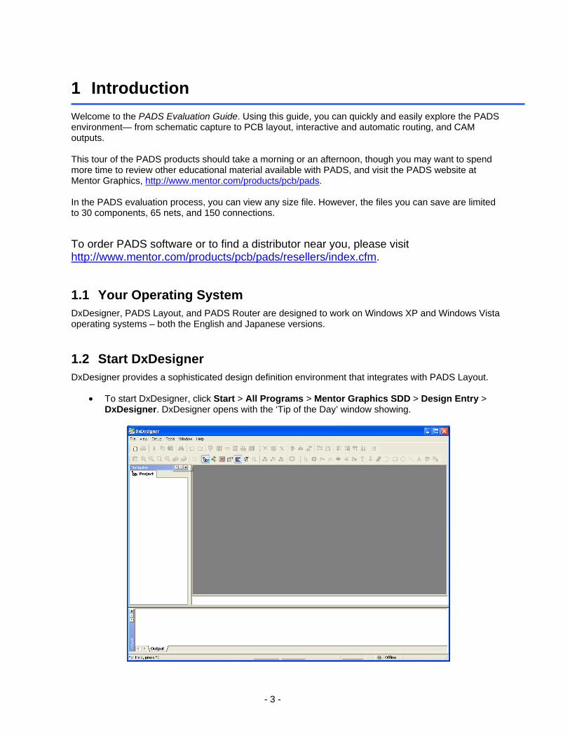
1 Introduction Welcome to the PADS Evaluation Guide. Using this guide, you can quickly and easily explore the PADS environment— from schematic capture to PCB layout, interactive and automatic routing, and CAM outputs. This tour of the PADS products should take a morning or an afternoon, though you may want to spend more time to review other educational material available with PADS, and visit the PADS website at Mentor Graphics, http://www.mentor.com/products/pcb/pads. In the PADS evaluation process, you can view any size file. However, the files you can save are limited to 30 components, 65 nets, and 150 connections. To order PADS software or to find a distributor near you, please visit http://www.mentor.com/products/pcb/pads/resellers/index.cfm.
1.1 Your Operating System DxDesigner, PADS Layout, and PADS Router are designed to work on Windows XP and Windows Vista operating systems – both the English and Japanese versions.
1.2 Start DxDesigner DxDesigner provides a sophisticated design definition environment that integrates with PADS Layout.
• To start DxDesigner, click Start > All Programs > Mentor Graphics SDD > Design Entry > DxDesigner. DxDesigner opens with the ‘Tip of the Day’ window showing.
- 3 -

1.3 DxDesigner Interface and Utilities DxDesigner has a flexible and easy-to-customize interface so you can organize your workspace in your own style. The most frequently used windows are:
• Project Navigator • Schematic Editor • Output Window
1.3.1 Project Navigator Use the Project Navigator — a familiar Windows-style Explorer tree — to browse through objects in the design project such as schematic sheets, symbols, and nets. It is also where you may make changes to the project such as schematic renaming, copying, sheet re-ordering, and sheet deletion.
- 4 -

1.3.2 Schematic Editor Use the Schematic Editor Window to place components, draw nets, buses, and more. It is used for creating both flat and hierarchical designs. An example of a schematic created in DxDesigner is shown below.
Sample DxDesigner schematic.
1.3.3 Output Window The Output Window displays the output results from commands. This window may have more than one tab. Each tool that produces results information (including warnings, error messages, and more) opens its own tab in the Output Window.
- 5 -

1.4 Hotkeys and Mouse operation DxDesigner and PADS Layout/Router use keyboard and mouse methods of navigation, making it easy for you to navigate in the way that most suits your working style. DxDesigner offers several ways to pan, zoom, and scroll. You can use the menus, keyboard, mouse, or any combination of these to navigate through your schematics. With the keyboard, you can:
• Zoom In (F7) • Zoom Out (F8) • Zoom to Full sheet (Home) • Center on pointer (Insert)
With the mouse, you can:
• Scroll Up/Down (Press Middle Mouse button and move mouse up/down) • Scroll Left/Right (Press Middle Mouse button and move mouse left/right) • Zoom In/Out (Scroll Mouse wheel)
See also: Chapter 9, DxDesigner Keyboard Shortcut Commands. PADS Layout and Router offer several ways to pan, zoom, and scroll. You can use the menus, keyboard, mouse, or any combination of these to navigate your designs. With the keyboard, you can:
• Zoom In (Page Up) • Zoom Out (Page Down) • Zoom to Full sheet (Home) • Center on pointer (Insert)
With the mouse, you can:
• Scroll Up/Down (Mouse wheel) • Scroll Left/Right (SHIFT+Mouse wheel) • Zoom In/Out (Ctrl+Mouse wheel)
See also: Chapter 10, PADS Layout Keyboard Shortcut Commands.
- 6 -

1.5 DxDesigner Setup You can use the DxDesigner Settings to customize your design environment including, among others:
• Setting the default sheet size
• Setting your preferred color scheme
Customize your environment
• On the Setup menu, click Settings. The Settings dialog box opens.
Set sheet size and border
1. In Left panel, in the “Schematic Editor” grouping, select New Sheets.
2. Change the Size for the sheet to B.
3. Select the Automatically add border to new schematic sheets check box to force DxDesigner to automatically add a border to newly added sheets.
4. Click Apply to confirm your choices.
- 7 -

Configure display objects colors
1. In Left panel, in the Display grouping, click Objects.
2. Scroll down to the Net row. Click the box in the Color column of the Net row.
3. Select the color you want for your nets. Tip: Note the effect in the Preview window.
4. Click OK to confirm your changes and close the dialog box.
- 8 -

2 The PADS Evaluation Circuit The PADS Evaluation Circuit The circuit shown below will be used to introduce you to the PADS design flow using DxDesigner as the schematic capture tool. To save time, the design is available in various stages of development. If you find you are pressed for time, you can open one of the partially finished versions to use with the exercises. The files are located in C:\PADS Projects\Samples.
The circuit shown below will be used to introduce you to the PADS design flow using DxDesigner as the schematic capture tool. To save time, the design is available in various stages of development. If you find you are pressed for time, you can open one of the partially finished versions to use with the exercises. The files are located in C:\PADS Projects\Samples. Schematic Layout Schematic Layout Eval_blank\Eval.prj Layout_Eval_Outline.pcb Eval_blank\Eval.prj Layout_Eval_Outline.pcb Eval_start\Eval.prj Layout_Eval_PrePlaced.pcb Eval_start\Eval.prj Layout_Eval_PrePlaced.pcb Eval_partial\Eval.prj Layout_Eval_Placed.pcb Eval_partial\Eval.prj Layout_Eval_Placed.pcb Eval_done\Eval.prj Layout_Eval_Routed.pcb Eval_done\Eval.prj Layout_Eval_Routed.pcb
Layout_Eval_Done.pcb Layout_Eval_Done.pcb
Sch_Eval_Done.sch
Layout_Eval_Done.pcb
- 9 -
3 System Design with DxDesigner System Design with DxDesigner This section begins the design process with the DxDesigner schematic capture program. This section begins the design process with the DxDesigner schematic capture program.
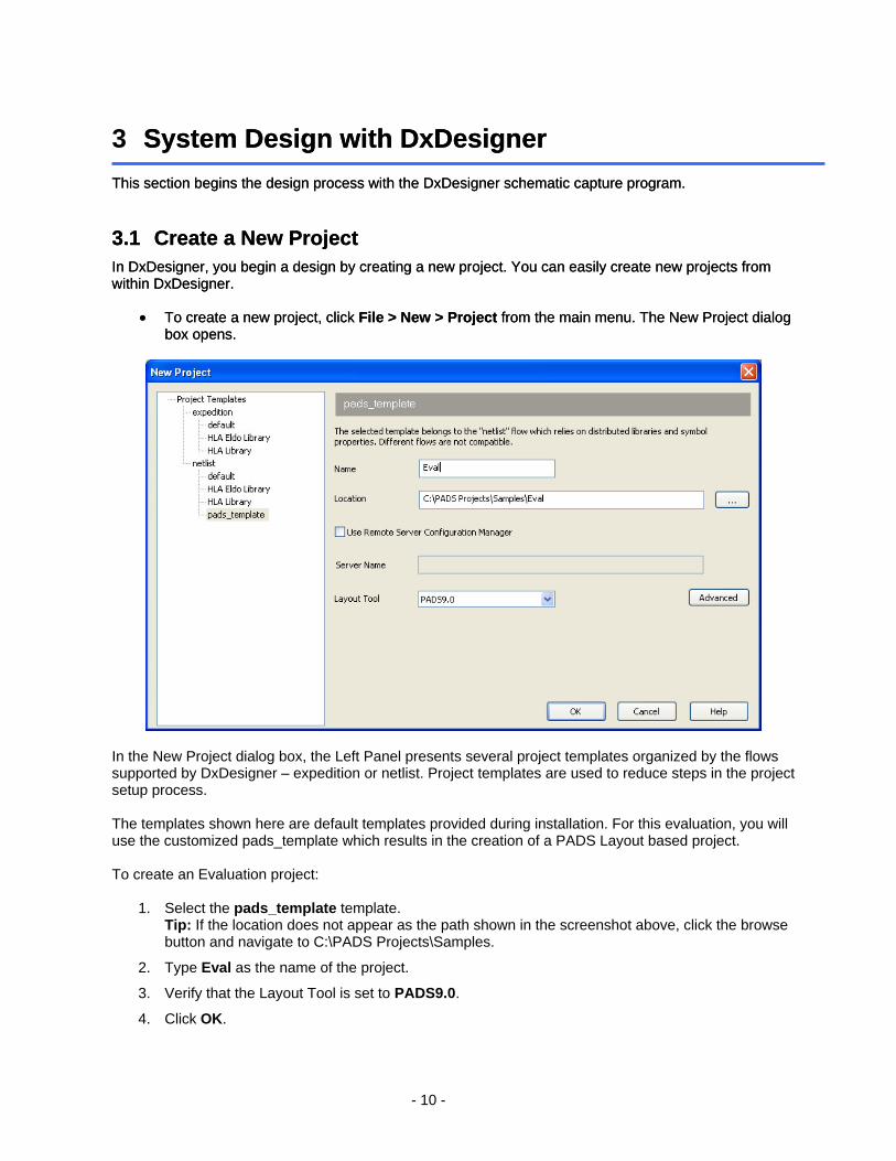
3.1 Create a New Project 3.1 Create a New Project In DxDesigner, you begin a design by creating a new project. You can easily create new projects from within DxDesigner. In DxDesigner, you begin a design by creating a new project. You can easily create new projects from within DxDesigner.
• To create a new project, click File > New > Project from the main menu. The New Project dialog box opens.
• To create a new project, click File > New > Project from the main menu. The New Project dialog box opens.
In the New Project dialog box, the Left Panel presents several project templates organized by the flows supported by DxDesigner – expedition or netlist. Project templates are used to reduce steps in the project setup process. The templates shown here are default templates provided during installation. For this evaluation, you will use the customized pads_template which results in the creation of a PADS Layout based project. To create an Evaluation project:
1. Select the pads_template template. Tip: If the location does not appear as the path shown in the screenshot above, click the browse button and navigate to C:\PADS Projects\Samples.
2. Type Eval as the name of the project.
3. Verify that the Layout Tool is set to PADS9.0.
4. Click OK.
- 10 -

3.2 Add a new Schematic
Now that you created a project, you will add a new schematic.
• On the File menu, point to New, and then click Schematic.
A new blank schematic is added with a blank sheet border. This is a result of setting the ‘Automatically add border to new schematic sheets’ option in section 1.5. Tip: You can easily change the border. With nothing selected, right-click and click Change Border.
- 11 -
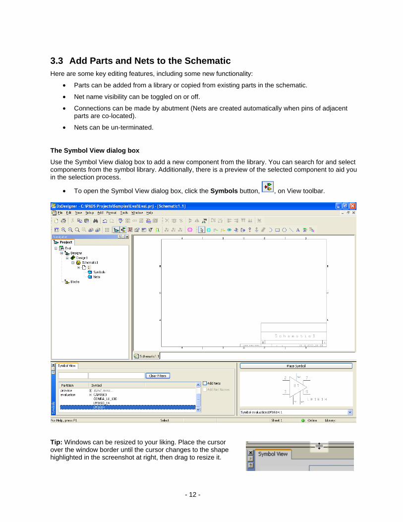
3.3 Add Parts and Nets to the Schematic Here are some key editing features, including some new functionality:
• Parts can be added from a library or copied from existing parts in the schematic.
• Net name visibility can be toggled on or off.
• Connections can be made by abutment (Nets are created automatically when pins of adjacent parts are co-located).
• Nets can be un-terminated.
The Symbol View dialog box
Use the Symbol View dialog box to add a new component from the library. You can search for and select components from the symbol library. Additionally, there is a preview of the selected component to aid you in the selection process.
• To open the Symbol View dialog box, click the Symbols button, , on View toolbar.
Tip: Windows can be resized to your liking. Place the cursor over the window border until the cursor changes to the shape highlighted in the screenshot at right, then drag to resize it.
- 12 -
Placing and Wiring Parts
Place and wire the following parts from the library: CONRA-11-100, LM161H
1. Using the Symbols View window, expand the “evaluation” symbols partition.
2. Select the LM161H symbol. The symbol graphics are shown in the Preview area.
3. Click the Place Symbol button and move the pointer into the open sheet.
4. Click to place an instance of the component on the center of the sheet.
5. Press Esc to exit Place Symbol mode. Tip: You can use F7 to zoom in, F8 to Zoom out and F6 to center the screen on the cursor.
6. Repeat the place symbol process to add an instance of the CONRA_11_100 symbol just to the left of pin 2 of the LM161H part.
7. Press Esc to exit Place Symbol mode.
Tip: You can add a single instance of a component without needing to press Esc after adding to the sheet. Drag the symbol from the preview area and drop it onto the sheet.
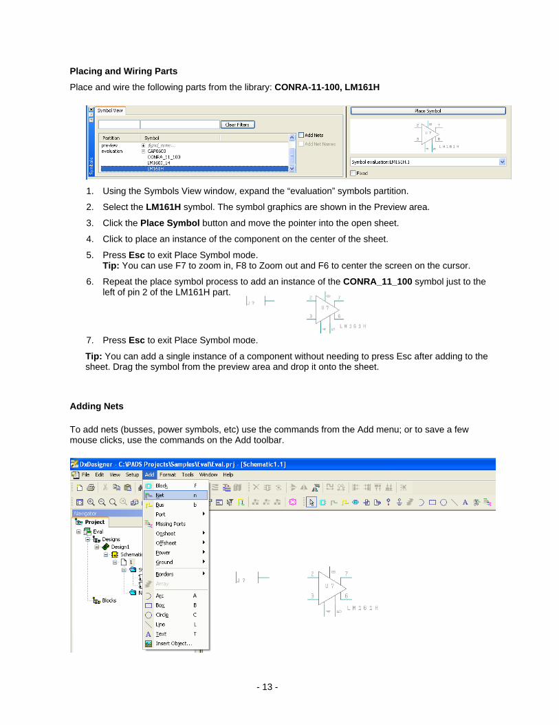
Adding Nets
To add nets (busses, power symbols, etc) use the commands from the Add menu; or to save a few mouse clicks, use the commands on the Add toolbar.
- 13 -

1. To Add a connector pin to the input pin, on the Add toolbar, click the Add Net button, . Tip: You can also use the n key as a shortcut.
2. Press and hold the left mouse button at CONRA_11_100 connector pin and drag a new net over to pin 2 of the LM161H. Release the mouse button to complete the net.
3. To add a power symbol, click the Power button, , from the Add toolbar. Click 5v.1 and place an instance of the symbol above the LM161H symbol. Click to place the power symbol. Right-click to exit the Add Special Component mode.
4. To add a Ground symbol, click the Ground button, , from the Add toolbar. Click gnd.1 and place an instance of the symbol below the LM161H symbol. Right-click to exit the Add Special Component mode.
5. Connect pin 8 of LM161H to power symbol. Do the same with pin 3 and pin 4 of LM161H – connect them to ground symbol.
6. When you finish adding nets, click the Select button, , on the Add toolbar to exit Add Net mode.
- 14 -
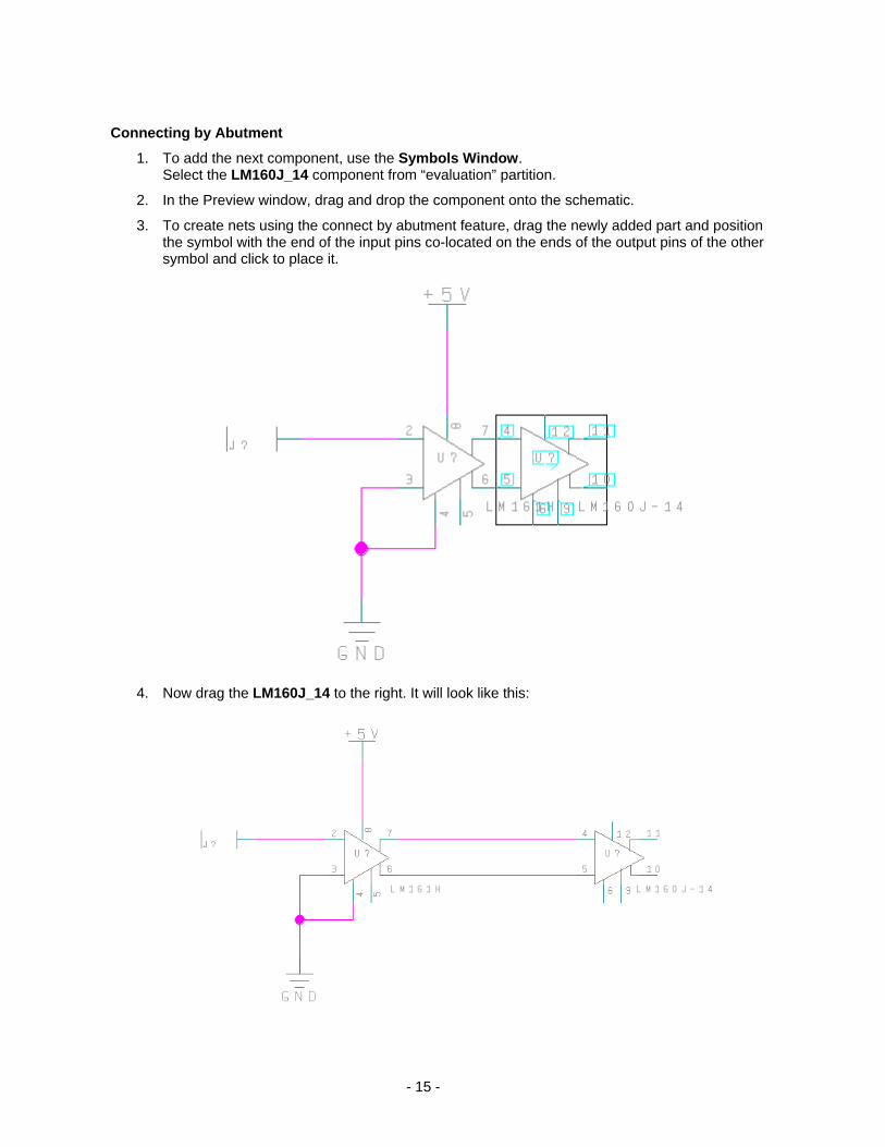
Connecting by Abutment
1. To add the next component, use the Symbols Window. Select the LM160J_14 component from “evaluation” partition.
2. In the Preview window, drag and drop the component onto the schematic.
3. To create nets using the connect by abutment feature, drag the newly added part and position the symbol with the end of the input pins co-located on the ends of the output pins of the other symbol and click to place it.
4. Now drag the LM160J_14 to the right. It will look like this:
- 15 -

Adding an Alternate Version of a symbol
1. In the Symbol View window, select the CONTRA-11-100 symbol from the evaluation list.
2. In the preview area, select the alternate CONTRA-11-10.2 symbol from the dropdown list in the eenshot above).
nt, he schematic.
6. Add additional symbols and nets to match the schematic as shown below.
Preview Area (see scr
3. Click Place Symbol.
4. Place the symbol on the schematic adjacent to the second LM160J_14 symbol.
5. Add the next instance of CONTRA-11-100 (from Symbol View or by copying it). Tip: You can copy a component that was just placed on the schematic, select the componepress Ctrl while you drag and drop a copy of the selected component onto t
7. Place a CAP0603 symbol, 2 additional CONTRA-11-100 symbols, Power and Ground symbols. Then connect them as shown below.
- 16 -

The completed schematic looks like the following:
Naming Nets
1. Click the Filter button, , on the main toolbar to open the selection filter.
2. Unselect all and then select Net. You can close the Filter window.
3. Click the Selection button, , to enter selection mode.
4. Select the net between pin 11 of LM160J_14 and CONRA_11_100.
5. Right-click and click Properties.
6. In the Properties dialog box, add the net name OUT_DATA_NEG.
7. Name the net between pin 10 of LM160J_14 and CONRA_11_100 as OUT_DATA_POS.
- 17 -

3.4 Saving the Schematic You may have noticed that saving your work is not a step in any of the above procedures. You may have also noticed that there is no Save button in DxDesigner. This is simply because it is not necessary with the client/server architecture. Any changes are dynamically written to the database.
- 18 -

4 PCB Design with PADS Layout Before continuing with the design, let’s review the highlights of PADS Layout. PADS Layout features:
• Easy-to-use design, placement, manual routing, CAM outputs
• Advanced constraint management
• Communications link between schematic and layout
• Full ECO forward/backward support
• Physical Design Reuse (PDR)
• Advanced Packaging and Chip-On-Board Toolkits
• Split/mixed planes support
• Fabrication Verification (DFF)
• Design For Test (DFT)
PADS Layout users are able to create wireless designs such as cell phones, cell repeater stations, satellite communication, automotive FOBS, and any other RF/Microwave application. With every seat of PADS Layout you can:
• Import complex copper shapes and line geometries into the Decal Editor
• Shield crucial traces for efficient channel/co-planar waveguide design
• Stitch areas with Via Arrays for complex copper-pour areas with specific pattern requirements
• Provide greater conductivity between planes on different layers
• Minimize noise susceptibility
• Create precise outlines and square & chamfered corner geometry, and output them in Gerber
- 19 -

4.1 Starting PADS Layout Open PADS Layout, add the library for this evaluation and get familiar with the PADS Layout environment.
• Click Start > All Programs > Mentor Graphics SDD > PADS 9.0 > Design Layout & Routing > PADS Layout.
Adding the PADS Eval library to the library list
1. On the File menu, click Library to open the Library Manager.
2. Click the Manage Lib. List button.
3. In the Library List dialog, click the Add Button.
4. In the Add Library dialog, browse to, and select the PADS_Eval.pt* library in the following folder. C:\MentorGraphics\9.0PADS\SDD_HOME\Libraries
5. Click Open to add the library to the library list. Tip: Any library can be re-positioned in the search order list using the Up or Down buttons.
6. In the Library List dialog, click OK.
7. Click Close to close the Library Manager.
- 20 -
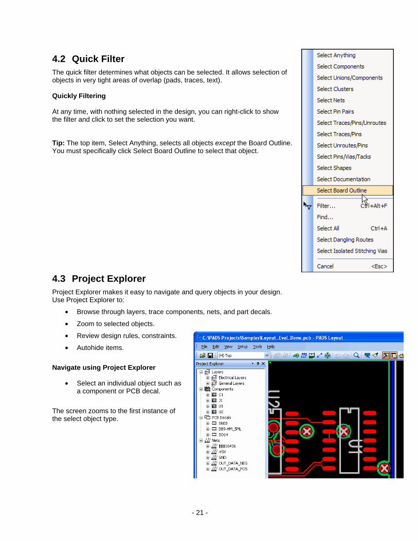
4.2 Quick Filter The quick filter determines what objects can be selected. It allows selection of objects in very tight areas of overlap (pads, traces, text). Quickly Filtering At any time, with nothing selected in the design, you can right-click to show the filter and click to set the selection you want. Tip: The top item, Select Anything, selects all objects except the Board Outline. You must specifically click Select Board Outline to select that object.
4.3 Project Explorer Project Explorer makes it easy to navigate and query objects in your design. Use Project Explorer to:
• Browse through layers, trace components, nets, and part decals.
• Zoom to selected objects.
• Review design rules, constraints.
• Autohide items.
Navigate using Project Explorer
• Select an individual object such as a component or PCB decal.
The screen zooms to the first instance of the select object type.
- 21 -

4.4 Board Outline Creation It is simple to create board outlines in PADS Layout, though you can also import outlines from other drafting packages such as AutoCAD via the DXF/IDF format.
Use the Board Outline and Cutout tool to:
• Create board outlines quickly and efficiently.
• Include board cutout areas, routing/part keepouts.
Tip: You can press the Page Up key to zoom in, the Page Down key to zoom out, or the Insert key to center the view on the cursor location.
Creating simple board outline
1. Click the Drafting Toolbar button, , to open the Drafting toolbar.
2. Click the Board Outline and Cutout button, .
3. Move the cursor to the design area, right-click and click Rectangle.
4. Type S0 0 (S zero space zero) and press Enter to place the pointer at the origin.
5. Press the Spacebar to start the rectangle at the design origin.
6. Type S2000 1000 and press Enter to place the pointer at X/Y 2000/1000.
7. Press the Spacebar to locate the corner and complete the board outline.
8. Press Home to zoom to the board outline.
1000 mils
2000 mils
The PADS Eval Board Outline Optional: Select the board outline and try the Move and Split options.
Save the PCB Design
• Click the Save button, , and save the file as Eval_outline.pcb.
- 22 -
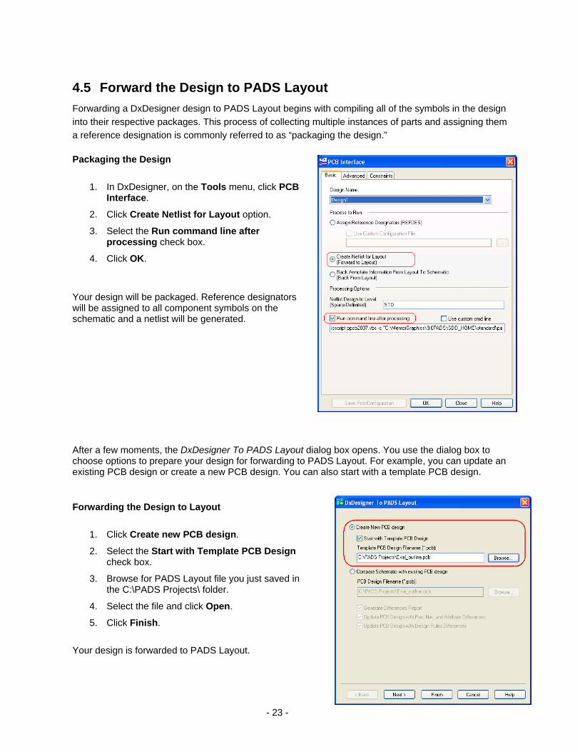
4.5 Forward the Design to PADS Layout Forwarding a DxDesigner design to PADS Layout begins with compiling all of the symbols in the design into their respective packages. This process of collecting multiple instances of parts and assigning them a reference designation is commonly referred to as “packaging the design.”
Packaging the Design
1. In DxDesigner, on the Tools menu, click PCB
Interface.
2. Click Create Netlist for Layout option.
3. Select the Run command line after processing check box.
4. Click OK.
Your design will be packaged. Reference designators will be assigned to all component symbols on the schematic and a netlist will be generated. After a few moments, the DxDesigner To PADS Layout dialog box opens. You use the dialog box to choose options to prepare your design for forwarding to PADS Layout. For example, you can update an existing PCB design or create a new PCB design. You can also start with a template PCB design.
Forwarding the Design to Layout
1. Click Create new PCB design.
2. Select the Start with Template PCB Design check box.
3. Browse for PADS Layout file you just saved in the C:\PADS Projects\ folder.
4. Select the file and click Open.
5. Click Finish.
Your design is forwarded to PADS Layout.
- 23 -

In PADS Layout you will now see the parts placed at the board origin and your board outline.
Dispersing Components
1. In PADS Layout, on the Tools menu, click Disperse Components.
2. At the “OK to start dispersion?” prompt, click Yes.
The components are placed outside the board perimeter as shown.
- 24 -

4.6 DxDesigner Link Use DxDesigner Link to:
• Select or highlight objects between the DxDesigner schematic and PADS Layout
• Select or highlight objects between the DxDesigner schematic and PADS Router
• Compare Schematic-to-PCB
• Transfer design rules and ECO
• The links provide push-button, bi-directional synchronization.
Activate the DxDesigner Link
• To open DxDesigner Link, in PADS Layout click Tools > DxDesigner.
Use the Documents Tab of DxDesigner Link to connect a schematic in DxDesigner with a layout design in PADS Layout for forward and backward annotation and cross-probing.
1. In the DxDesigner Project File area browse to the name of your DxDesigner project file, C:\PADS Projects\Samples\Eval\Eval.prj, and click Open, then click Connect.
When the connection of both files is successful, the Compare Designs, Forward to PCB and Backward from PCB buttons are available.
• You can click Compare Designs to compare and report the differences between the schematic and layout design files.
• You can click Forward to PCB to open the Forward Annotation dialog box. • You can click Backward from PCB to open the Backward Annotation dialog box.
- 25 -
5 PADS Design Rules and Constraints PADS Design Rules and Constraints Design rules are stored in a schematic project database and in PCB design files. Design rules you set up in DxDesigner are automatically transferred when you import the netlist into PADS Layout. Design rules you set up in PADS Layout are automatically available when you open the design in PADS Router.
Design rules are stored in a schematic project database and in PCB design files. Design rules you set up in DxDesigner are automatically transferred when you import the netlist into PADS Layout. Design rules you set up in PADS Layout are automatically available when you open the design in PADS Router. Design rules: Design rules:
• Save time and virtually eliminate human error due to miscommunication between engineers and designers.
• Save time and virtually eliminate human error due to miscommunication between engineers and designers.
• Allow the engineer to tag critical nets. • Allow the engineer to tag critical nets.
• Allow the designer to maintain absolute design control. • Allow the designer to maintain absolute design control.
• Enable you to specify design rule priority• Enable you to specify design rule priority.
• Can be set so designs are not over-constrained, making them easier to route.
• Can be assigned in either DxDesigner, PADS Layout, or PADS Router.
• Are carried in the design.
• Extended rules (high speed rules like differential pair rules) are optional.
- 26 -
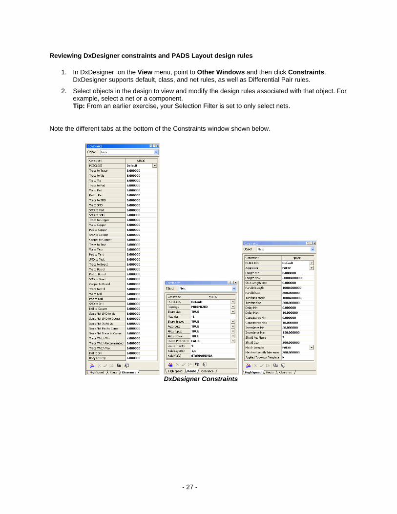
Reviewing DxDesigner constraints and PADS Layout design rules
1. In DxDesigner, on the View menu, point to Other Windows and then click Constraints. DxDesigner supports default, class, and net rules, as well as Differential Pair rules.
2. Select objects in the design to view and modify the design rules associated with that object. For example, select a net or a component. Tip: From an earlier exercise, your Selection Filter is set to only select nets.
Note the different tabs at the bottom of the Constraints window shown below.
DxDesigner Constraints
- 27 -
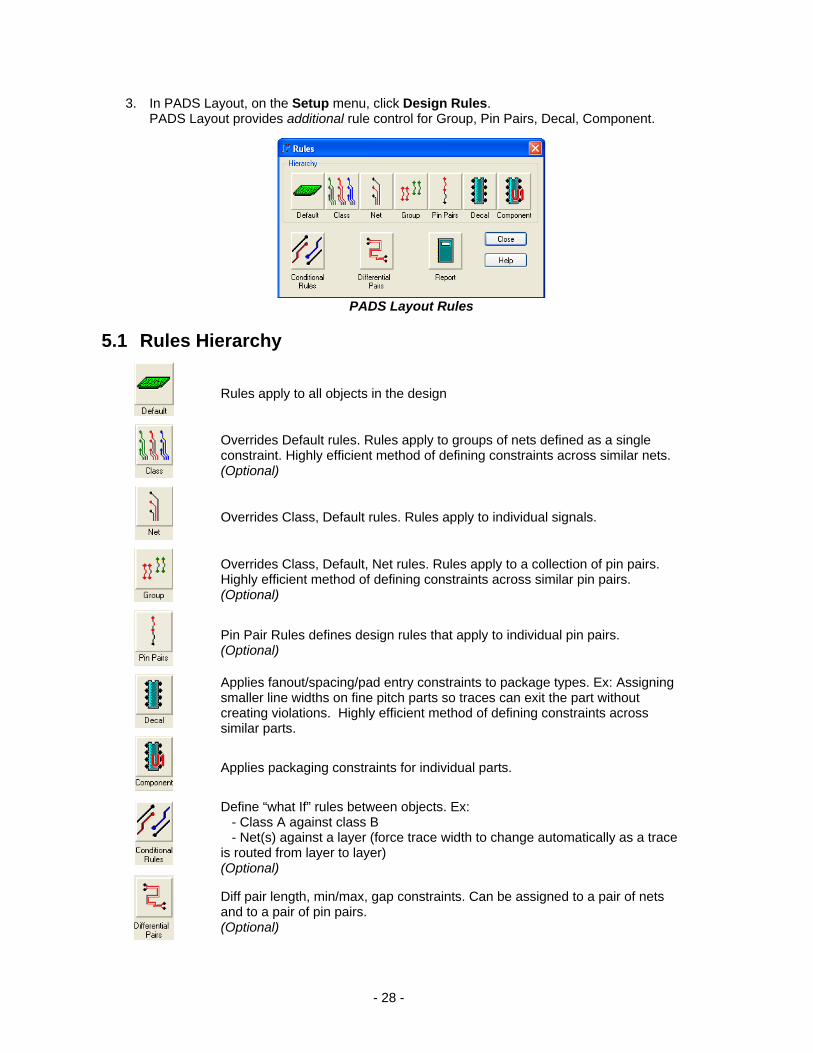
3. In PADS Layout, on the Setup menu, click Design Rules. PADS Layout provides additional rule control for Group, Pin Pairs, Decal, Component.
PADS Layout Rules
5.1 Rules Hierarchy
Rules apply to all objects in the design
Overrides Default rules. Rules apply to groups of nets defined as a single constraint. Highly efficient method of defining constraints across similar nets. (Optional)
Overrides Class, Default rules. Rules apply to individual signals.
Overrides Class, Default, Net rules. Rules apply to a collection of pin pairs. Highly efficient method of defining constraints across similar pin pairs. (Optional)
Pin Pair Rules defines design rules that apply to individual pin pairs. (Optional)
Applies fanout/spacing/pad entry constraints to package types. Ex: Assigning smaller line widths on fine pitch parts so traces can exit the part without creating violations. Highly efficient method of defining constraints across similar parts.
Applies packaging constraints for individual parts.
Define “what If” rules between objects. Ex: - Class A against class B - Net(s) against a layer (force trace width to change automatically as a trace is routed from layer to layer) (Optional)
Diff pair length, min/max, gap constraints. Can be assigned to a pair of nets and to a pair of pin pairs. (Optional)
- 28 -

5.2 Rule Categories
Clearances for trace, package body, drill; Trace width settings
Trace topology, copper-sharing, protect/push and shove controls, layer biasing, maximum # of vias
Min/max rules for parallelism, matched length, delay, capacitance which are then viewed in a report. (Optional)
SMD pad patterns - alignment, direction, length, via spacing.
Location and angles for pad-to-trace intersections. Placing vias on SMD pads.
- 29 -

5.3 Net Constraints Constraints are special rules applied to objects such as critical traces, and are adhered to by the interactive router and the autorouter, as well as by the design rule checking routines. Constraints travel with the schematic database. Constraints can be crucial in the design of high speed PCBs. With constraints, you can:
• Apply design parameters to a hierarchy of design objects (default, class, group, etc.)
• Tag critical nets as differential pairs, min/max and matched lengths.
Assign Constraints in PADS Layout You can assign constraints quickly with easy-to-use dialogs. Assign default trace widths min/rec/max as 4/6/8 respectively. Also, assign two signals as differential pairs, with a min length of 1000 mils and a max length of 4000 mils. The signals are listed under Nets in Project Explorer as follows: Netnames Constraints OUT_DATA_NEG, OUT_DATA_POS
Diff pair; min. length=1000 mils, max. length=4000 mils
1. In PADS Layout, on the Setup menu, click Design Rules.
2. Click Default, then Clearance.
3. Set trace widths as depicted.
4. Click OK to exit Clearance Rules.
5. Click Close to exit Default Rules.
- 30 -
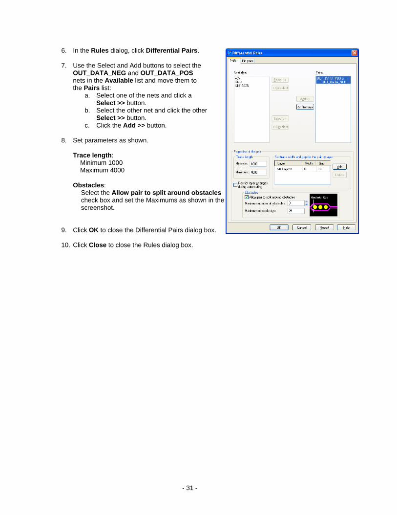
6. In the Rules dialog, click Differential Pairs.
7. Use the Select and Add buttons to select the OUT_DATA_NEG and OUT_DATA_POS nets in the Available list and move them to the Pairs list:
a. Select one of the nets and click a Select >> button.
b. Select the other net and click the other Select >> button.
c. Click the Add >> button.
8. Set parameters as shown. Trace length: Minimum 1000 Maximum 4000 Obstacles:
Select the Allow pair to split around obstacles check box and set the Maximums as shown in the screenshot.
9. Click OK to close the Differential Pairs dialog box.
10. Click Close to close the Rules dialog box.
- 31 -

5.4 Component Placement Since designers spend a significant amount of time placing components, PADS provides the ultimate in component placement capability. With PADS Layout, you can place components individually or by group.
There are multiple placement techniques:
• Drag & Drop
• X and Y coordinates
• Sequential move – parts snap to cursor
• Radial-array placement for circular (for example, DUT) board applications
Single Part Placement
1. Right-click and click Select Components to set the component filter.
2. Type G100 and press Enter to set the placement grid to 100 mils.
3. Drag any component to move it.
4. Press Ctrl+R to rotate components as you move them. Place components at the location you want and click once to release the object.
Tip: While moving a component, you can press Esc to cancel. While not in an action mode, press Esc to deselect design objects that are selected.
Group Placement
1. With nothing selected, beginning in free space draw a rectangle around a group of components in order to select them all.
2. Drag any of the highlighted objects to move the entire group and click to place the group.
Using the above methods, place all components as shown below.
Re-positioning Reference Designators
1. Right-click and click Select Documentation.
2. Drag each reference designator to move it. Position the Reference Designators as shown above. Tip: Press the Tab key to rotate the component while moving it.
Tip: With any object selected, right-click to see and initiate all of the main commands possible with that object.
- 32 -

5.5 Vias Any type and any number of vias can be easily defined in PADS Layout. The default via type in PADS is called a STANDARDVIA. Vias are:
• Created through an intuitive menu
• Available as through-hole and partial via types
Changing the Via Value To change the size of the STANDARDVIA to a smaller via:
1. Click Setup > Pad Stacks from the main menu.
2. In the Pad Stack Type area, select Via.
3. Select <Start> from the Sh: Sz: Layer list.
4. Type 40 in the Diameter box. Tip: When you change the value in the Diameter box, you must click another box for the value to register.
5. Repeat for <Inner Layers> and <End> layers.
6. Type 24 in the Drill Size box.
7. Select OK to close the dialog box.
8. Click “Yes” when prompted by the message “Are you sure you want to change all vias of type STANDARDVIA”.
Note how easy it would be to set up Partial or Slotted vias.
- 33 -
5.6 Layer Setup The interactive router, autorouter, and CAM Photoplot generator need the layer setup information. There are 2 methods to create plane layers:
• Split/Mixed (preferred, WYSIWYG method)
• CAM (outmoded method using negative imagery)
Use layer setup to:
• Change layer count
• Easily assign signal, plane, split/mixed layers
• Set routing direction biasing
• Re-assign layers
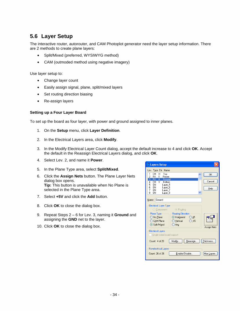
Setting up a Four Layer Board To set up the board as four layer, with power and ground assigned to inner planes.
1. On the Setup menu, click Layer Definition.
2. In the Electrical Layers area, click Modify.
3. In the Modify Electrical Layer Count dialog, accept the default increase to 4 and click OK. Accept the default in the Reassign Electrical Layers dialog, and click OK.
4. Select Lev. 2, and name it Power.
5. In the Plane Type area, select Split/Mixed.
6. Click the Assign Nets button. The Plane Layer Nets dialog box opens. Tip: This button is unavailable when No Plane is selected in the Plane Type area.
7. Select +5V and click the Add button.
8. Click OK to close the dialog box.
9. Repeat Steps 2 – 6 for Lev. 3, naming it Ground and assigning the GND net to the layer.
10. Click OK to close the dialog box.
- 34 -

Assigning Colors by Layer Assign Colors by Layer as follows:
Top Red Inner Layer 2 Light Blue Inner Layer 3 Green Bottom Dark blue
Assign Design Items as follows:
Errors Magenta
1. Click Setup > Display Colors from the
main menu.
2. Select a color box, then the layer or object
you want.
3. Click OK to close the dialog box.
4. Click the Save button, , to save your design.
Tip: It’s easy to switch visible layers using the Layer modeless command: L1 - reveals top layer color (red) L4 - reveals bottom layer color (green)
5.7 Passing the Design to PADS Router The design is now ready for PADS Router – the advanced interactive design environment. You can choose to either interactively route or autoroute your design on its own; even while you work on another design in PADS Layout. PADS Router provides:
• Simple, push-button transfer to/from either PADS Router interactive router or PADS Autorouter
• Easy set up of the routing strategy
Pass the Design to PADS Router
• On the main toolbar, click the Switch to PADS Router button, .
- 35 -

6 Introduction to PADS Routing Solutions Introduction to PADS Routing Solutions PADS Router is an advanced interactive router and an autorouter. PADS Router is an advanced interactive router and an autorouter.
The PADS Router provides: The PADS Router provides:
• Powerful push n’ shove, plowing algorithms • Powerful push n’ shove, plowing algorithms
• High speed routing using shape-based, gridless technology
• High speed routing using shape-based, gridless technology
• Diff pair, min/max length, matched length • Diff pair, min/max length, matched length
• Semi-automatic 45°, 90°, and any-angle routing • Semi-automatic 45°, 90°, and any-angle routing
• Adherance to extensive design rule hierarchy • Adherance to extensive design rule hierarchy
• And intuitive, customizable environment • And intuitive, customizable environment
• Multiple interactive route operations: • Multiple interactive route operations:
• Autoroute by net, component • Autoroute by net, component
• Partial route (let autorouter finish) • Partial route (let autorouter finish)
• Automatic trace neck-down • Automatic trace neck-down
• Trace smoothing • Trace smoothing
• Auto-reroute of moved components • Auto-reroute of moved components
• Pin/via hopping • Pin/via hopping
• Pad entry control • Pad entry control
Guard bands dynamically display DRC boundaries of objects in route area
Multiple, advanced plowing modes
Critical net highlight
Real time trace length monitor indicates length constraint violations
Trace neck-down
- 36 -

6.1 Constraint Assignment and Review As mentioned in a prior section, PADS offers an extensive hierarchical constraint assignment capability. Using constraints, you can set critical net criteria either in the schematic tool or assign them in PADS Layout or PADS Router. Reviewing Constrained Nets in PADS Router To assign min/max length of 100/1500 to a net:
1. In Project Explorer, expand Net Objects then Nets, then expand the three unnamed nets beginning with the “$” to see their pin pair connections.
2. Select the net which connects U1.2 to J1.1. Make sure you select the $<net name> and not the pin pair.
3. Right-click and click Properties.
4. Click the Length tab. 5. Select the Restrict Length check box.
6. Type 100 in the Minimum length box.
7. Type 1500 in the Maximum length box.
Tip: Variations from default rules are indicated by a red icon on the tab label,
and a YELLOW highlight in the boxes. To see this now, click Apply.
8. Click OK to close the dialog box.
Confirming the Differential Constraints Confirm the differential constraints assigned earlier (Section 5.3) in the schematic are present. 1. In Project Explorer, expand Differential Pairs, and
click OUT_DATA_NEG<- > OUT_DATA_POS.
2. Right-click and click Properties. Notice the min/max trace length 1000/4000 transferred over from schematic.
3. Click OK to close the dialog box.
- 37 -

6.2 Interactive, High-Speed Routing Environment PADS Router offers the most highly functional interactive routing capabilities available in desktop PCB design. You will quickly note how intelligently traces “flow” around obstacles. You have the speed of autorouting, with the control of hand routing.
PADS Router provides:
• Toggle on/off Dynamic routing, loops, protecting, trace necking, obstacle control, display, pushing, smoothing
• Routing angle - Orthogonal, Diagonal, even true “any angle” routing
• Extensive dialogs controls both interactive and auto routing
• Accordion creation with fine tuning of amplitude and gap
• Extensive real-time Plower control
Set Layer Toggles Set the layer pair to Top and Bottom. To determine what layers are toggled when interactively routing:
1. On the Tools menu, click Options.
2. Click the Routing tab.
3. Select 4 – Bottom from the Second Layer list.
4. Click OK.
Set the Routing Grid To set the routing grid:
1. On the Edit menu, click Properties.
2. Click the Grid tab.
3. In Routing row, type 10 in both the X Increment, and Y Increment columns.
4. Click OK to close the dialog box.
- 38 -

Switching Layers
There are three ways to switch between layers.
1. Use Layers List in the main toolbar. 2. During interactive routing, press F4 to
toggle between layer pairs. 3. Use the Layers modeless command.
(Type L 1 for layer 1) (Type L 4 for layer 4)
Routing Interactively
Start interactive routing:
Select J1, pin 1 (the square pin of the connector).
1. Select J1 pin 1 (the square pin of the connector).
2. Right-click and click Interactive Route or press F3. Note how the trace length monitor changes color as you route the length past 1500 mils.
3. Press F4 to toggle between the top and bottom layers. Tip: Press Backspace to go backwards and remove corners.
4. Click the ending pin of the connection you are routing. Tip: Double-click while routing to autocomplete the route.
5. To route the differential pairs, Select either OUT_DATA_NEG or OUT_DATA_POS (J1.2 or J1.3), and press F3.
Note how the paired net also highlights and routes.
- 39 -
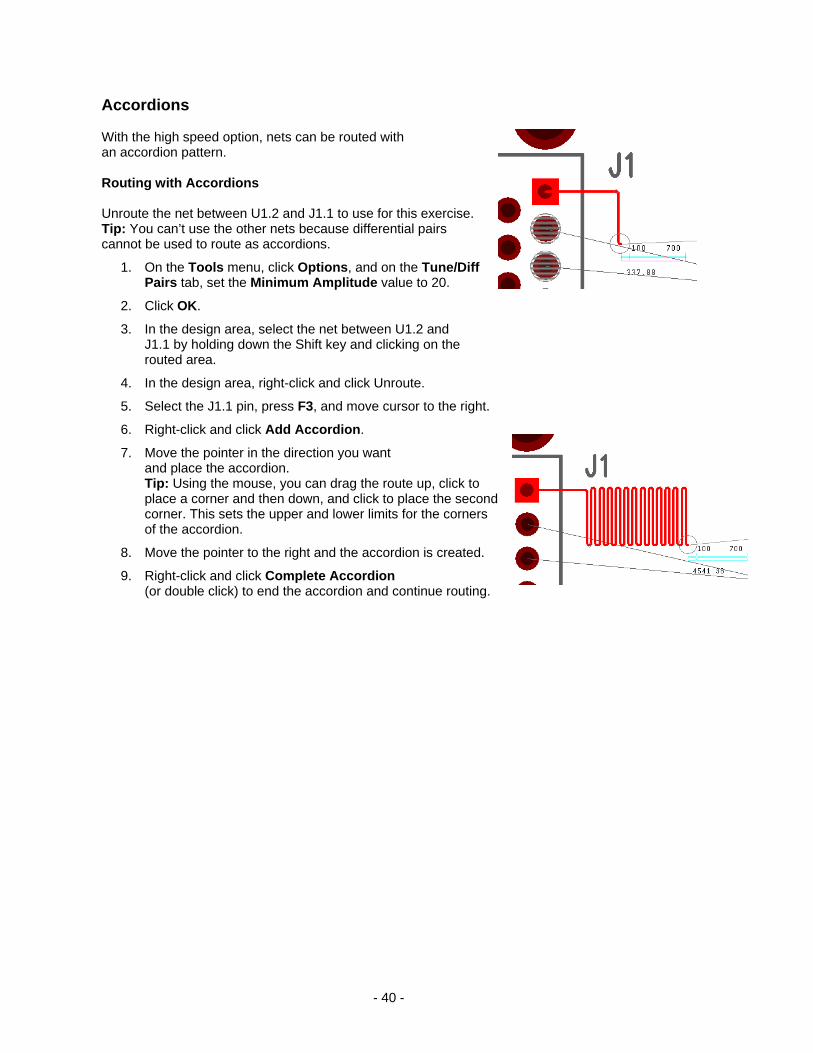
Accordions With the high speed option, nets can be routed with an accordion pattern. Routing with Accordions Unroute the net between U1.2 and J1.1 to use for this exercise. Tip: You can’t use the other nets because differential pairs cannot be used to route as accordions.
1. On the Tools menu, click Options, and on the Tune/Diff Pairs tab, set the Minimum Amplitude value to 20.
2. Click OK.
3. In the design area, select the net between U1.2 and J1.1 by holding down the Shift key and clicking on the routed area.
4. In the design area, right-click and click Unroute.
5. Select the J1.1 pin, press F3, and move cursor to the right.
6. Right-click and click Add Accordion.
7. Move the pointer in the direction you want and place the accordion. Tip: Using the mouse, you can drag the route up, click to place a corner and then down, and click to place the second corner. This sets the upper and lower limits for the corners of the accordion.
8. Move the pointer to the right and the accordion is created.
9. Right-click and click Complete Accordion (or double click) to end the accordion and continue routing.
- 40 -

Other Route Modes Try the various route modes that are available as a right-click as you route the board. Tip: This menu is available only when you are actively routing. Interactive modes While routing a trace, try these modes … … End (before reaching target pad) … Arcs … changing Width, Layer … changing Routing Angle … toggle on/off Dynamically Route … toggle on/off Push Trace Behind ... toggle on/off Plow After Click
To smooth a trace that “meanders” around the board:
1. Select a trace segment that isn’t a direct connection.
2. Right-click and click Select Trace.
3. Right-click and click Smooth Trace Pattern.
To route some traces and “push” a trace through the routed traces using the plow mode:
1. On the Tools menu, click Options.
2. Click the Routing tab.
3. Change the Plower settings to see what they do.
Interactively route the remainder of the board.
A sample, finished board, interactively routed.
- 41 -

6.3 PADS AutoRouter The PADS AutoRouter is a shape-based gridless autorouter that is designed for high speed, high density designs. Great for fine pitch parts and dense areas alike, it uses the same routing algorithms as the PADS Router interactive router.
The PADS Autorouter can be set to route:
• Entire design
• Specific parts
• Critical nets, net class
The PADS AutoRouter features:
• Intuitive route strategy dialogs
• No complex programming languages to learn
• Fast learning cycle
• Low, Medium, High controls based on available routing time/density.
• Protect Routing to protect traces after a completed pass.
• Fanout, cleanup, tuning route passes
Autoroute a Design
1. On the File menu, click Open.
2. Select …\Samples\Layout_Eval_Placed.pcb and click Open.
3. Before routing, run the Pre-Routing Analysis tool to check the board for any potential problems prior to autorouting.
4. Group-select the entire design by dragging the cursor over all objects – all nets and comps highlight in the selection color.
5. On the Tools menu, click Pre-routing Analysis. The Output Window opens, and may display a warning that the three critical nets cannot be routed since the net lengths exceed the assigned constraint, depending on how far the pins are. Notice that it may recommend moving components or relaxing the constraint values, depending on component placement.
- 42 -

Route the power and ground fanouts. 1. On the Tools menu, click Options.
2. Click the Strategy tab.
3. Clear the Route and Optimize check boxes.
4. Select the Pass checkbox for the Fanout Pass Type.
5. In the Routing order definition section, expand the Net Objects and then the Nets grouping.
6. Select the +5V and GND nets and click Selected to add them to the routing order.
7. In the Routing Order list, click All Nets and then click the red X button to remove it from the list.
8. In the Pass definition area, click to clear any remaining Pass Types. The dialog box should match the screenshot at right.
9. Click OK to close the dialog box.
10. On the Tools menu, point to Autoroute and then click Start to run the autorouter. The resulting board looks like this:
- 43 -

Route the signal nets.
1. On the Tools menu, click Options.
2. Click the Strategy tab.
3. Clear the Fanout Pass check box.
4. Click the Route Pass check box. The dialog should match the screenshot at right.
5. Click OK to close the dialog box.
6. Press F9 to route.
The resulting board looks similar to:
7. Run an Optimize pass using the same technique.
Unroute the entire board and try other Intensity settings.
8. Right-click and click Select Traces/Pins to select the traces on the entire board.
9. Right-click and click Select All.
10. Press Backspace to unroute.
11. Alter the Intensity setting in the Strategy Options and try rerouting.
12. Save the completely routed design.
13. Click the Switch to PADS Layout button, , to open the routed design in PADS Layout.
- 44 -
6.4 Create Copper Pour in PADS Layout PADS Layout features a powerful and flexible copper pour capability.
With PADS Layout copper pour you can:
• Easily create power/ground/signal copper planes on any layer.
• Create copper “cut out” areas for copper voiding.
• Create “positive image” power/ground planes.
• Run extensive checking utilities to ensure proper plane interconnects.
• Support buried trace applications.
• Automatically create thermal pads.
To add a ground copper area to the bottom layer:
1. In PADS Layout, type L4 and press Enter to switch to the bottom layer (layer 4).
2. Click the Drafting toolbar button, , to open the Drafting toolbar.
3. Click the Copper Pour button, .
4. Create a complete polygon in an area inclusive of some ground pins, like this using double-click to complete the polygon:
- 45 -

The Add Drafting dialog box opens automatically when you complete the polygon:
5. Select the GND net from the Net list and click OK.
Now you must select the outline and flood it.
6. Press Esc to exit the copper pour draw mode. The shape should remain selected. Tip: If the shape is not selected, right-click and click Select Shapes to select the outline.
7. Right-click and click Flood.
8. Click Yes to Proceed with flood. The board looks something like this:
Notice that the ground pins are connected to the copper areas with thermal relief pads, and the copper clears if traces exist on that layer.
- 46 -

6.5 Design verification In addition to realtime design rule checking (DRC), PADS provides several very powerful design rule audits to ensure that your design accurately represents the schematic. Several checks are included with every copy of PADS, while a few others are options. Design verification includes:
• Numerous clearance checks.
• Checks that ensure all nets have been routed.
• High speed checks such as length, delay, capacitance.
• Check to ensure maximum via count isn’t exceeded.
• Plane connectivity check.
Running Various Design Verifications
1. On the Tools menu, click Verify Design. The Verify Design dialog box opens.
2. To run the various checks, click the check type (for example, Clearance) and then click Start.
- 47 -
6.6 CAM Outputs PADS produces reliable laser photoplotting files of the highest accuracy. In addition to gerber files, it also creates all manufacturing support files and documentation including drill data, DirectCAM, and other standard data exchange formats.
PADS CAM output provides:
• Intuitive, menu-driven board fabrication data generation
• Gerber photoplot output
• Excellon drill data
• Standard print/plot output
• Bill of Materials output for calculating board cost
Generating Gerber Files for Signal, Plane Layers To set up the CAM directory:
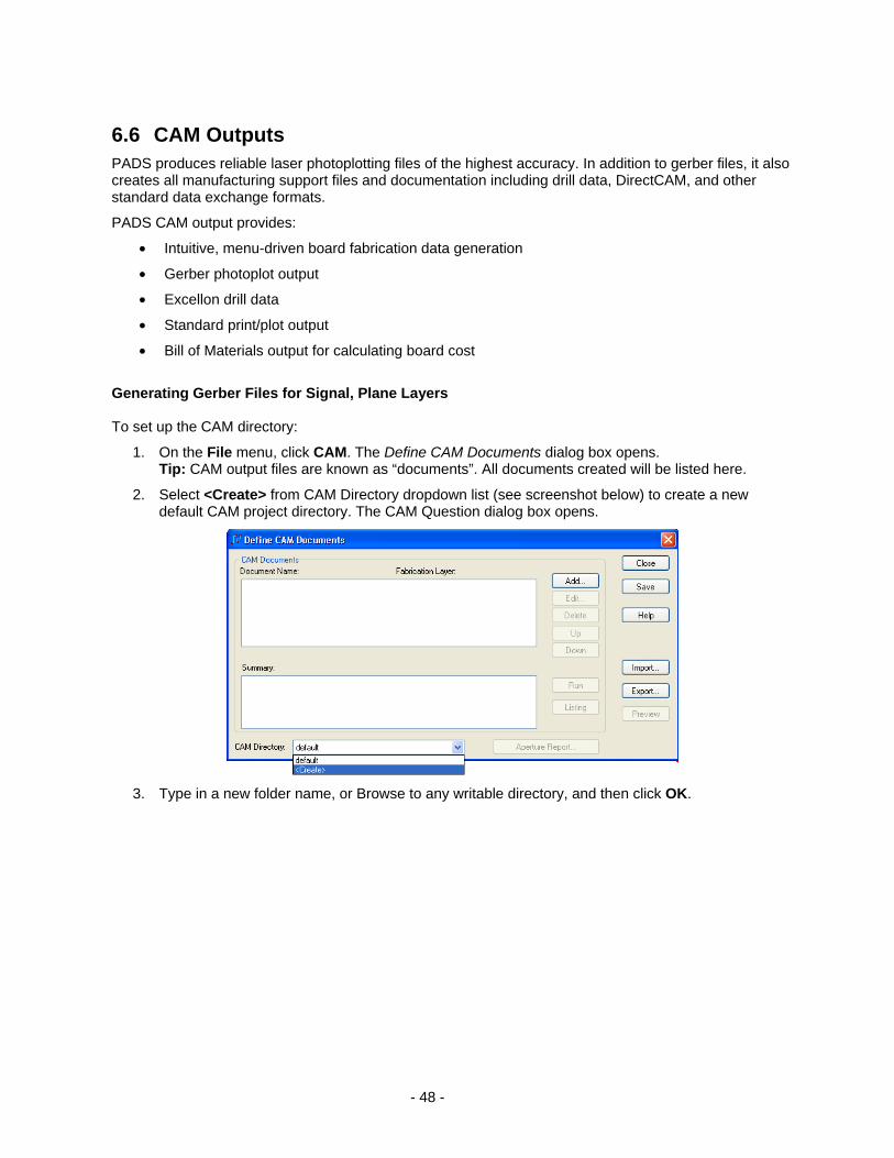
1. On the File menu, click CAM. The Define CAM Documents dialog box opens. Tip: CAM output files are known as “documents”. All documents created will be listed here.
2. Select <Create> from CAM Directory dropdown list (see screenshot below) to create a new default CAM project directory. The CAM Question dialog box opens.
3. Type in a new folder name, or Browse to any writable directory, and then click OK.
- 48 -

Create the Top, Signal Layer
1. Click Add to create a new document. The Add Document dialog box opens. You will create a basic top layer Gerber file.
2. Fill out the Add Document dialog. Document Name: L1-TOP Document Type: Routing/Split Plane. Click Ok to Leave Layer Association as Top. Output File: Use the default name The dialog box should match the screenshot at right.
Review the Customize Document Options
1. Click Layers to select the elements to include in the photoplot for that particular layer. The Select Items dialog box opens.
2. Click Cancel to close the dialog box.
- 49 -

3. Click Options to select offset, mirroring, Ref Des suppression, over/undersizing pads and more. The Plot Options dialog box opens.
4. Click Cancel to close the dialog box.
5. Click Preview Selections (lower left).
6. Click Board to zoom in to the graphic image in the lower left corner. This is what the Gerber file should look like, depending on your results.
7. Click Close to close the Preview window.
8. Click Run in the Add Document window to generate the Gerber file.
9. Click Yes to complete the operation.
10. Click OK to close the Add Document dialog.
You generated the top layer, photoplot file.
- 50 -

Generating a Gerber file for the Power mixed/split plane #2 Tip: You may have already assigned the +5V and GND nets as split/mixed layers to levels 2 and 3 respectively in Setup > Layer Definition, so the correct pads will receive thermal reliefs when the photoplots are generated. If you have not, do so now.
1. In the Define CAM Documents dialog box, click Add.
2. Name this layer L2-PWR.
3. Select Routing/Split Plane from the Document Type list. The Layer Association window opens.
4. In the Layer list, select Power and click OK. The system defaults to the typical elements necessary to generate this layer (see Layers).
5. Click Yes for each dialog box.
6. Repeat for layers 3, 4, and silkscreen, etc. The final photoplots resemble these images. Layer 1 – top Layer 2 – power
- 51 -

Layer 3 – ground Layer 4 – bottom
- 52 -
7 Other PADS Layout Highlights
7.1 Automation OLE Automation is the Microsoft Standard for passing and exporting information and embedding Documents. PADS uses Automation to communicate seamlessly with other applications to pass information and/or embed documents.
7.2 Attribute support PADS has extensive attribute support. PADS attributes give you:
• Tight integration with other company applications.
• Support for custom attributes.
• Attribute checking upon file import.
• Export to any OLE compliant tool.
• Definition using intuitive dialogs.
- 53 -

8 Other PADS Options Other PADS Options
8.1 Design For Fabrication (DFF) Audit 8.1 Design For Fabrication (DFF) Audit In addition to standard design rule checking (DRC) spacing violations, PADS offers a very powerful feature called Design For Fabrication (DFF). DFF performs a variety of fabrication design rule checks, flagging potential fabrication areas before
In addition to standard design rule checking (DRC) spacing violations, PADS offers a very powerful feature called Design For Fabrication (DFF). DFF performs a variety of fabrication design rule checks, flagging potential fabrication areas before sending the design to the fabrication shop. DFF provides checks for:
• Acid traps
• Copper slivers
• Soldermask slivers
• Traces in soldermask opening
• Silkscreen over pads
• And more
8.2 Testpoint Creation and Checking (DFT Audit option) The DFT Audit (Design For Test) option reduces costly design iterations and ensures the testability of your designs before fabrication. A unique aspect of DFT is that testpoints are assigned during the initial routing passes, unlike other post-assignment solutions that try to fit them in after the design is complete. The DFT audit provides two functions – testpoint assignment (routing) and testpoint coverage reports (audits). With DFT, you can:
• Screen designs for In Circuit Test (ICT) adaptability.
• Assign/verify design testability as seen from the bottom side (typical default).
• Assign/verify testpoints for “Clamshell” (both sides) type fixtures.
• Define testability constraints for various technologies/densities. These can be stored and reused.
• Validate probes. Check for clearances such as probe to probe, probe to trace, probe to board edge.
• Generate custom reports. Reports are generated with every test point name and X/Y location including nets with missing test points. Designers can use this complete report to determine what action to take in order for the design to pass testability requirements.
- 54 -
8.3 Physical Design Reuse (PDR) PDR is a unique and powerful capability for saving portions of PCB layout designs for reuse. With the PDR option, previously proven and tested sections of circuitry can stored and reused by anyone in the organization. Such re-using design data is essential for many companies to meet their aggressive time schedules. With PDR, you can:
• Easily reuse “building blocks” based on existing design elements, such as Multi Channel design, Concurrent Design and RF Microwave circuit replication.
• Include all design elements such as parts, traces, copper, etc.
• Have schematic independent information, which eliminates the need for time-consuming ECO’s
• Save valuable redesign time from one project to the next.
8.4 Advanced Packaging And COB Toolkit PADS Layout also offers a sophisticated advanced packaging and chip-on-board toolkit option, which provides high density connectivity through sophisticated route wizards.
This option gives you:
• Automated, any-angle BGA package routing.
• Auto-connection generation.
• Substrate array pad fanout with plating tail creation.
• Automated Die and Die Flag creation wizard.
8.5 Assembly Variants PADS has extensive variant support through this option. Variants are created with a consistent based of components and then altered to redefine components as Installed, Non-Installed and Substituted. This allows a single base from which modifications can be made in the core design only once.
Bills of Materials (BOMs) are created from an assembly option that features both installed parts, uninstalled parts and substituted parts identifying the status of those parts.
Assembly drawings can be created based on assembly options and include or exclude parts from the actual drawing based on the status in the variant.
- 55 -
8.6 Mechanical Data Import/Export This PADS Layout option provides seamless, accurate transfer of IDF mechanical data such as board outline, component packaging, and drafting documentation. Two primary exchange formats are supported:
DXF Link • Bidirectional interface to AutoCAD compatible systems.
• No need to recreate complex work done by mechanical engineer.
IDF Interface • Bidirectional interface with 3D software packages.
• No need to recreate complex work done by mechanical engineer.
• Pass placement requirements and height restrictions bi-directionally
- 56 -

9 DxDesigner Keyboard Shortcut Commands Tip: Print this out and keep it handy. Command Action Ctrl+C Edit Copy Ctrl+V Edit Paste Ctrl+Delete Edit Delete Ctrl+X Edit Cut Ctrl+Backspace Edit Redo Ctrl+Z Edit Undo F1 Help Ctrl+F1 Help on DxDesigner
Help Topics Shift+F1 Help Context Ctrl+P File Print Ctrl+N File New Ctrl+O Block Open Ctrl+Alt+G Project Settings Ctrl+Q or Alt+Enter
Properties
Ctrl+S File Save s Select Mode f Add Block Shift+Space Add Power Pin Ctrl+Shift+Space Add Hierarchical Pin n Add Net L Add Line b Add Bus
Command Action A Add Arc B Add Box T Add Text C Add Circle Ctrl+Shift+F Flip F4 Mirror Ctrl+R Reattach Net m Move Now Ctrl+Shift+R or F3
Rotate 90 degrees
Ctrl+Y Cycle y Push Symbol h Push Schematic Page Up Prior Page Page Down Next Page F6 or Insert Pan
Ctrl+W Zoom Area z View Zoom Z View Zoom Selected
F7 Zoom In F8 Zoom Out Home Zoom Full Shift+F10 View Restore Zoom
Space Command Line
- 57 -
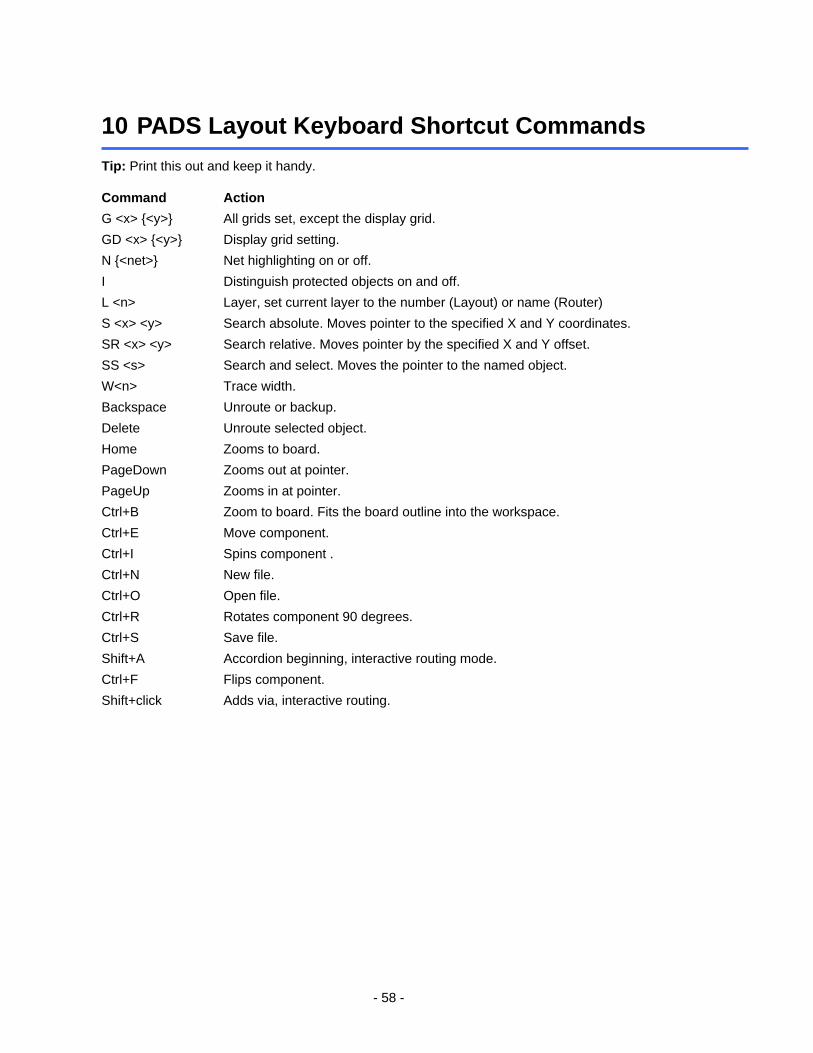
10 PADS Layout Keyboard Shortcut Commands Tip: Print this out and keep it handy. Command Action G <x> {<y>} All grids set, except the display grid. GD <x> {<y>} Display grid setting. N {<net>} Net highlighting on or off. I Distinguish protected objects on and off. L <n> Layer, set current layer to the number (Layout) or name (Router) S <x> <y> Search absolute. Moves pointer to the specified X and Y coordinates. SR <x> <y> Search relative. Moves pointer by the specified X and Y offset. SS <s> Search and select. Moves the pointer to the named object. W<n> Trace width. Backspace Unroute or backup. Delete Unroute selected object. Home Zooms to board. PageDown Zooms out at pointer. PageUp Zooms in at pointer. Ctrl+B Zoom to board. Fits the board outline into the workspace. Ctrl+E Move component. Ctrl+I Spins component . Ctrl+N New file. Ctrl+O Open file. Ctrl+R Rotates component 90 degrees. Ctrl+S Save file. Shift+A Accordion beginning, interactive routing mode. Ctrl+F Flips component. Shift+click Adds via, interactive routing.
- 58 -
11 Default Non-Electrical Layer Assignment 1 Default Non-Electrical Layer Assignment
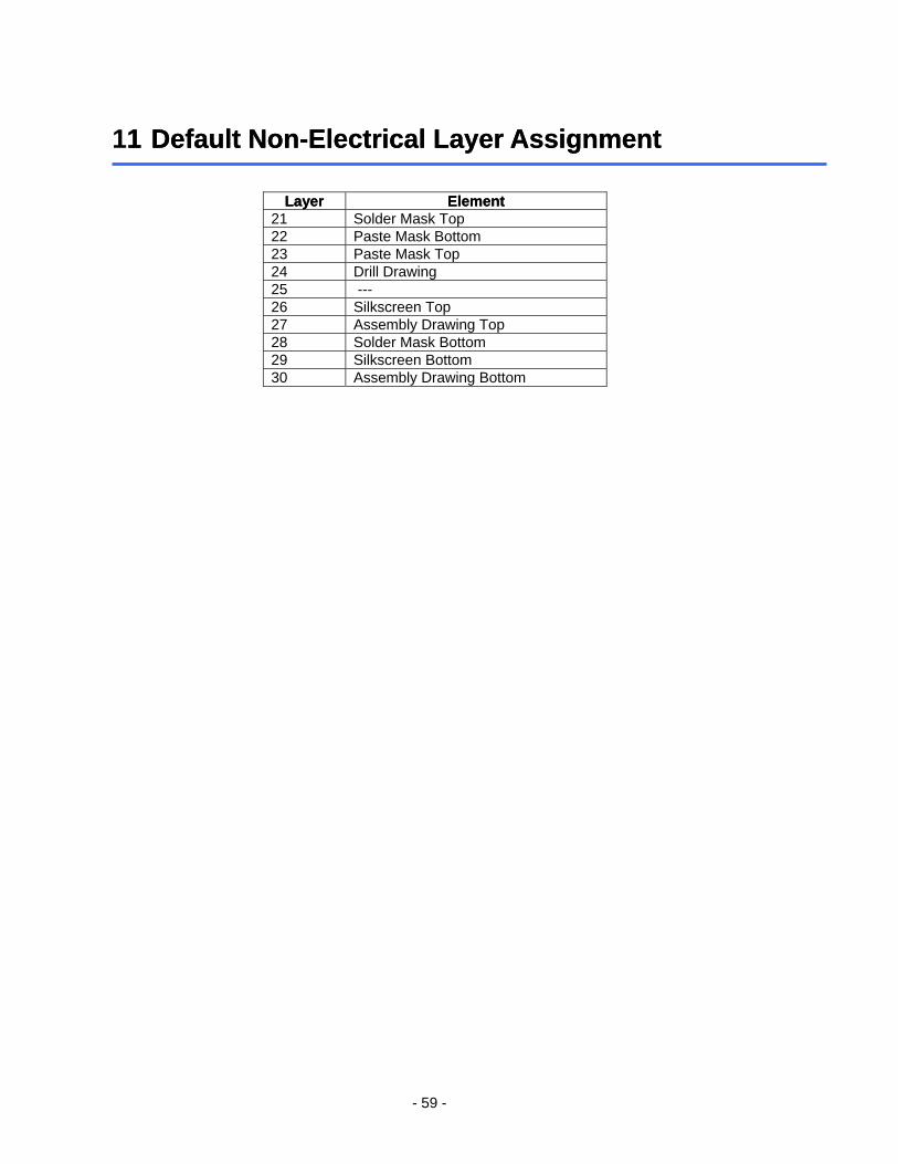
Layer Layer Element Element 21 Solder Mask Top 22 Paste Mask Bottom 23 Paste Mask Top 24 Drill Drawing 25 --- 26 Silkscreen Top 27 Assembly Drawing Top 28 Solder Mask Bottom 29 Silkscreen Bottom 30 Assembly Drawing Bottom
- 59 -