SGBB GOVT POLYTECHNIC COLLEGE, SIROHI PCB ...
41
SGBB GOVT POLYTECHNIC COLLEGE, SIROHI CLASS TEST-II (SESSION 2017-18) SUB- ELECTRONICS COMPONENTS AND MATERIAL (EL201) Q-1 Explain silk screen process of making PCB. Ans: PCB Silkscreen printing technologies The name of the PCB silkscreen is derived from the actual process of using a stencil to apply ink to the PCB. This method is still used in some cases, but new methods have been devised in order to increase legibility and allow for smaller text height and line width. Liquid photo imaging, or LPI, is a process similar to the one used for the soldermask. Basically, a photoimageable film is exposed to UV light. The board has to be developed and cured after exposure. This approach allows for better resolution of text and artwork but the whole process will require more time. Direct legend printing, or DLP, is considered to be the best and fastest method for the application of the PCB silkscreen layer. Special inkjet printers are used in conjunction with acrylic ink that is cured while the actual printing is done, with UV light. The manual method requires a stencil of the text and artwork that is usually made of nylon. Epoxy ink (paste) is pushed through the stencil, using a squeegee board, onto the laminate. After
-
Upload
khangminh22 -
Category
Documents
-
view
0 -
download
0
Transcript of SGBB GOVT POLYTECHNIC COLLEGE, SIROHI PCB ...

SGBB GOVT POLYTECHNIC COLLEGE, SIROHI
CLASS TEST-II (SESSION 2017-18)
SUB- ELECTRONICS COMPONENTS AND MATERIAL (EL201)
Q-1 Explain silk screen process of making PCB.
Ans:
PCB Silkscreen printing technologies
The name of the PCB silkscreen is derived from the actual process of using a stencil to apply ink
to the PCB. This method is still used in some cases, but new methods have been devised in order
to increase legibility and allow for smaller text height and line width.
Liquid photo imaging, or LPI, is a process similar to the one used for the soldermask. Basically,
a photoimageable film is exposed to UV light. The board has to be developed and cured after
exposure. This approach allows for better resolution of text and artwork but the whole process
will require more time.
Direct legend printing, or DLP, is considered to be the best and fastest method for the application
of the PCB silkscreen layer. Special inkjet printers are used in conjunction with acrylic ink that is
cured while the actual printing is done, with UV light.
The manual method requires a stencil of the text and artwork that is usually made of nylon.
Epoxy ink (paste) is pushed through the stencil, using a squeegee board, onto the laminate. After

this process is complete, the board has to be baked in order for the ink to cure. Although this
method is fairly fast and the stencils are easy to produce, it gives the least precise results. As a
comparison, the minimum text height for manual screen printing is 35 mil with some
manufacturers having a 50 mil limit, while the DLP method allows for text heights of 20 mil.
In a today`s high density designs, where being able to reduce text size but maintain legibility
is desirable, direct legend printing seems to be the method of choice. However, you should make
note of the fact that not all manufacturers are equipped with DLP technology. Also, the acrylic
ink will not cure on boards with silver finishes.
Q-2 Write a short notes on impregnation plant.
Ans:
Impregnation is process of applying a coating or layers of chemically stable liquids to porous
surfaces (like casting) or objects with inherent voids (like motor coils) to prevent accumulation
of undesired elements like dust, dirt, chemicals or water. Impregnation of objects improves its
physical properties and also tends to improve overall parameters of the equipment/component
wherein use. For Ex. a varnish impregnated coil improves the overall insulation resistance of the
motor and hence the life of the motor is improved.
Different chemicals are used in the process of the impregnation. These chemicals can be
classified as epoxy, varnish and resins. Impregnation process itself can be classified in different
types like flood impregnation, dip impregnation, vacuum impregnation, vacuum pressure
impregnation, trickle impregnation, hot roll dipped impregnation. Flood impregnation and dip
impregnation are simple impregnation processes often used in the low voltage small frame
electrical motors. In flood impregnation the resin/varnish is flooded in the chamber where the
preheated coils (electric motor stator or wound rotor) are placed. The coils are kept for soaking
in varnish for a certain period and then taken off to the baking oven. The varnish is stored in a
cold chamber or vessel called the storage tank. Typically temperatures for maintaining the
varnish/ resins is 15 deg C to 10 deg C. In dip impregnation, coils are dipped in a tank that
contains varnish and kept for a certain time.

Vacuum pressure impregnation is a special process designed to impregnate the motor coils or
some castings that are used in critical applications. Vacuum pressure Impregnation often called
the VPI process impregnates the coils or metal castings under vacuum. Impregnation under
vacuum prevents advent of external moisture that may be accumulated in the voids of the coil or
may be absorbed in insulation. Vacuum impregnated coils are free of moisture that result good
electrical properties.
In case of metal impregnation, vacuum impregnation results good adhesion of the chemical with
the surface. Metal impregnation process that involves impregnation of castings is often
accompanied by additional processes like cleaning of castings jobs, chemical treatment for better
adhesion etc. Often epoxy is used for porosity sealing of the castings.
In a typical vacuum pressure impregnation system for motors, preheated coils are kept in the
impregnation tank and vacuum is drawn. After a certain period resin is introduced in the
impregnation tank in controlled manner and filled till the top of the coil stack. Dry air or nitrogen
pressure is applied in the chamber for better penetration of the resin in the voids and this is
maintained for a stipulated time.
Later the resin is withdrawn to the storage tank. Almost in all the impregnation processes the
resin or varnish transfer from tank to tank is achieved by pressure difference in the two tanks or
by gravity flow of the varnish.
Q-3 Write a short notes on Auto Transformer.
Ans:
An Auto Transformer is a transformer with only one winding wound on a laminated core. An
auto transformer is similar to a two winding transformer but differ in the way the primary and
secondary winding are interrelated. A part of the winding is common to both primary and
secondary sides. On load condition, a part of the load current is obtained directly from the supply
and the remaining part is obtained by transformer action. An Auto transformer works as
a voltage regulator.
In an ordinary transformer, the primary and the secondary windings are electrically insulated
from each other but connected magnetically as shown in the figure below and in auto transformer
the primary and the secondary windings are connected magnetically as well as electrically. In
fact, a part of the single continuous winding is common to both primary and secondary.
There are two types of auto transformer based on the construction. In one type of transformer,
there is continuous winding with the taps brought out at convenient points determined by desired
secondary voltage and in another type of auto transformer, there are two or more distinct coils
which are electrically connected to form a continuous winding. The construction of Auto
transformer is shown in the figure below.

Figure : Auto – Transformer
The primary winding AB from which a tapping at C is taken, such that CB acts as a
secondary winding. The supply voltage is applied across AB, and the load is connected
across CB. The tapping may be fixed or variable. When an AC voltage V1 is applied across
AB, an alternating flux is set up in the core, as a result, an emf E1 is induced in the winding
AB. A part of this induced emf is taken in the secondary circuit.
Let,
V1 – primary applied voltage
V2 – secondary voltage across the load
I1 – primary current
I2 – load current
N1 – number of turns between A and B
N2 – number of turns between C and B

Neglecting no load current, leakage reactance and losses,
V1 = E1 and V2 = E2
Therefore the transformation ratio
As the secondary ampere-turns are opposite to primary ampere turns, so the current I2 is in phase
opposition to I1. The secondary voltage is less than the primary. Therefore current I2 is more than
the current I1. Therefore, the resulting current flowing through section BC is (I2 – I1)
Advantages
Less costly
Better regulation
Low losses as compared to ordinary two winding transformer of the same rating.
Disadvantages
The secondary winding is not insulated from the primary winding.
If an auto transformer is used to supply low voltage from a high voltage and there is a break in
the secondary winding, the full primary voltage comes across the secondary terminal which is
dangerous to the operator and the equipment. So the auto transformer should not be used to for
interconnecting high voltage and low voltage system.
Used only in the limited places where a slight variation of the output voltage from input voltage
is required.
Applications
It is used as a starter to give upto 50 to 60% of full voltage to the stator of a squirrel cage
induction motor during starting.
It is used to give a small boost to a distribution cable, to correct the voltage drop.
It is also used as a voltage regulator
Used in power transmission and distribution system and also in the audio system and railways.

SGBB GOVT POLYTECHNIC COLLEGE, SIROHI
MAX TIME- 1 HR CLASS TEST-II (SESSION 2017-18) MAX MARKS-15
SUB- CIRCUIT ANALYSIS (EL202) DATE-29/01/2018
NOTE- ATTEMPT ALL THREE QUESTIONS.
(1) Write the statement of Maximum Power transfer theorem and prove it.
(2) In following circuit, find thevenin voltage and thevenin resistance across terminals A and B :-
(3) In following circuit, find Node voltages 𝑉1 and 𝑉2 :-
MODEL ANSWERS
Answer 1:-
Statement :-
The maximum power transfer theorem states that in a linear , bilateral DC
network , maximum power is delivered to the load when the load resistance is
equal to the internal resistance of a source.
If it is an independent voltage source, then its series resistance (internal
resistance Rs) or if it is independent current source, then its parallel resistance
(internal resistance Rs) must equal to the load resistance RL to deliver maximum
power to the load.

Proof of Maximum Power Transfer Theorem
The maximum power transfer theorem ensures the value of the load resistance ,
at which the maximum power is transferred to the load.
Consider the below DC two terminal network (left side circuit) , to which the
condition for maximum power is determined , by obtaining the expression of
power absorbed by load with use of mesh or nodal current methods and then
derivating the resulting expression with respect to load resistance RL.
But this is quite a complex procedure. But in previous articles we have seen that
the complex part of the network can be replaced with a Thevenin’s equivalent as
shown below.
The original two terminal circuit is replaced with a Thevenin’s equivalent circuit
across the variable load resistance. The current through the load for any value of
load resistance is
Form the above expression the power delivered depends on the values of RTH and
RL. However the Thevenin’s equivalent is constant, the power delivered from this
equivalent source to the load entirely depends on the load resistance RL. To find
the exact value of RL, we apply differentiation to PL with respect to RL and
equating it to zero as

Therefore, this is the condition of matching the load where the maximum power
transfer occurs when the load resistance is equal to the Thevenin’s resistance of
the circuit. By substituting the Rth = RL in equation 1 we get
The maximum power delivered to the load is,
Total power transferred from source is
PT = IL2 (RTH + RL)
= 2 IL2 RL …………….(2)
Hence, the maximum power transfer theorem expresses the state at which
maximum power is delivered to the load , that is , when the load resistance is
equal to the Thevenin’s equivalent resistance of the circuit. Below figure shows a
curve of power delivered to the load with respect to the load resistance.
Answer 2:-
Step 1:- Calculation of Thevenin Voltage (𝑉𝑡ℎ)
According to question terminals A & B are open, so current through 1 ohm
resistor is 0. So voltage through it 0. So 𝑉𝑡ℎ is voltage across 5A current source.
And 5A & 3 ohm are in parallel, so 𝑉𝑡ℎ is across 3 ohm resistance.

So our circuit is
Applying KCL at node P, I1 + I2 + I3 = 0
𝑉𝑡ℎ−10
2 +
𝑉𝑡ℎ
3 - 5 = 0 →
3𝑉𝑡ℎ−30+2𝑉𝑡ℎ
6 = 5
5𝑉𝑡ℎ = 60
𝑉𝑡ℎ = 60
5 = 12 volt.
Step 2:- Calculation of thevenin resistance (𝑅𝑡ℎ)
For this independent sources (voltage, current ) are replace by their internal
resistances. So 10V voltage source is short-circuit and 5A current source is open-
circuited.
In above circuit, 2 ohm and 3 ohm resistance are in parallel, so net resistance is
=2∗3
2+3 =
6
5 ohm
So Thevenin resistance 𝑅𝑡ℎ = 6
5 + 1 =
11
5ohm

Answer 3:-
Applying KCL at node 1
𝑉 1 − 𝑉2
2 +
𝑉1
5 +
𝑉1− 10
1 = 0 →
5𝑉1− 5𝑉2+ 2𝑉1+ 10𝑉1− 100
10 =
0
17𝑉1 - 5𝑉2 = 100 …………….. (1)
Applying KCL at node 2
𝑉2− 𝑉1
2 +
𝑉2
10 - 2 =0 →
5𝑉2− 5𝑉1+𝑉2− 20
10 = 0
6𝑉2 − 5𝑉1 = 20 ……………….. (2)
Equation 1 is multiply with 6 and equation 2 is multiply with 5 and adding both
102𝑉1 - 30𝑉2 = 600
-25𝑉1 + 30𝑉2 = 100 → 77𝑉1 = 700 → 𝑉1 = 700
77 = 9.09
Put 𝑉1 in equation (2), we get
6𝑉2 - 5*9.09 = 20 → 6𝑉2 = 20 – 45.45
𝑉2 = −25.45
6 = -4.241

SGBB GOVT POLYTECHNIC COLLEGE, SIROHI
MAX TIME- 1 HR CLASS TEST-II (SESSION 2017-18) MAX MARKS-15
SUB- ELECTRONIC MEASUREMENT & INSTRUMENTATION (EL203) DATE-25/01/2018
NOTE- ATTEMPT ANY THREE QUESTIONS.
1) Explain construction and working of PMMC instrument.
2) Explain LVDT transducer.
3) Explain classification of instruments.
MODEL ANSWERS
Answer 1:-
Permanent Magnet Moving Coil Instrument
The permanent magnet moving coil instrument or PMMC type instrument uses
two permanent magnets in order to create stationary magnetic field. These types
of instruments are only used for measuring the DC quantities as if we apply AC
current to these type of instruments the direction of current will be reversed
during negative half cycle and hence the direction of torque will also be reversed
which gives average value of torque zero. The pointer will not deflect due to high
frequency from its mean position showing zero reading. However it can measure
the direct current very accurately.
Construction
A coil of thin wire is mounted on an aluminum frame (spindle) positioned
between the poles of a U shaped permanent magnet which is made up of
magnetic alloys like alnico.
The coil is pivoted on the jeweled bearing and thus the coil is free to rotate. The
current is fed to the coil through spiral springs which are two in numbers. The coil
which carries a current, which is to be measured, moves in a strong magnetic field
produced by a permanent magnet and a pointer is attached to the spindle which
shows the measured value.

Working:-
When a current flow through the coil, it generates a magnetic field which is
proportional to the current in case of an ammeter. The deflecting torque is
produced by the electromagnetic action of the current in the coil and the
magnetic field.
When the torques are balanced the moving coil will stop and its angular
deflection represents the amount of electrical current to be measured against a
fixed reference, called a scale. If the permanent magnet field is uniform and the
spring linear, then the pointer deflection is also linear.
The controlling torque is provided by two phosphorous bronze flat coiled helical
springs. These springs serve as a flexible connection to the coil conductors.
Damping is caused by the eddy current set up in the aluminum coil which
prevents the oscillation of the coil.
In moving coil instruments the deflecting torque is given by the expression:
Td = N*B*l*d*I where N is number of turns,
B is magnetic flux density in air gap,
l is the length of moving coil,
d is the width of the moving coil,
And I is the electric current.

Answer 2:-
Linear Variable Differential Transformer (LVDT):-
Construction:-
The device consists of a primary winding (P) and two secondary windings
named S1 and S2. Both of them are wound on one cylindrical former, side
by side, and they have equal number of turns. Their arrangement is such that they maintain symmetry with either side of the primary winding (P). A
movable soft iron core is placed parallel to the axis of the cylindrical former.
An arm is connected to the other end of the soft iron core and it moves
according to the displacement produced.
Working
As shown in the figure above, an ac voltage with a frequency between (50-400) Hz is supplied to the primary winding. Thus, two voltages VS1 and
VS2 are obtained at the two secondary windings S1 and S2 respectively.
The output voltage will be the difference between the two voltages (VS1-
VS2) as they are combined in series. Let us consider three different
positions of the soft iron core inside the former.
Null Position – This is also called the central position as the soft iron core will
remain in the exact center of the former. Thus the linking magnetic flux produced
in the two secondary windings will be equal. The voltage induced because of them
will also be equal. Thus the resulting voltage VS1-VS2 = 0.
Right of Null Position – In this position, the linking flux at the winding S2 has a
value more than the linking flux at the winding S1. Thus, the resulting voltage
VS1-VS2 will be in phase with VS2.
Left of Null Position – In this position, the linking flux at the winding S2 has a
value less than the linking flux at the winding S1. Thus, the resulting voltage VS1-
VS2 will be in phase with VS1.

From the working it is clear that the difference in voltage, VS1-VS2 will
depend on the right or left shift of the core from the null position. Also, the
resulting voltage is in phase with the primary winding voltage for the
change of the arm in one direction, and is 180 degrees out of phase for the
change of the arm position in the other direction.
The magnitude and displacement can be easily calculated or plotted by
calculating the magnitude and phase of the resulting voltage.
The graph above shows the plot between the resulting voltage or voltage
difference and displacement. The graph clearly shows that a linear function
is obtained between the output voltage and core movement from the null
position within a limited range of 4 millimeter. The displacement can be
calculated from the magnitude of the output voltage. The output voltage is
also displayed on a CRO or stored in a recorder.
Answer 3:-
Types of Electrical Measuring Instruments:
Electrical Instruments are basically classified into two types namely:
(A) Absolute Instruments
(B) Secondary Instruments
(A) Absolute Instruments:-
Absolute instruments are defined as the instruments that give deflections in
terms of physical constants and not measurable on a graduated scale.
The value of the electrical quantity to be measured are given by these
instruments.
The quantity are measured in terms of constants and from the deflection of the
instruments only.

Tangent galvanometer, Rayleigh current balance and absolute electrometer are
some of the examples of absolute instruments.
(B) Secondary Instruments:-
They are defined as the instruments that give a ready measure of the quantities
with the help of graduated scales.
The value of the electrical quantity to be measured is determined from the
deflection of these instruments.
With an absolute instrument these instruments are calibrated. ie, the secondary
instruments are compared with known standards or absolute instruments.
All the electrical measuring instruments belong to this category.
There are three categories of secondary instruments.
1. Indicating instruments
2. Recording instruments
3. Integrating instruments
1. Indicating Instruments:-
The value of the electrical quantity is indicated by these instruments at the time
when it is being measured. Pointers moving over the scale give the indication.
Ammeters, Voltmeters and wattmeters are the examples of these instruments.
2. Recording Instruments:-
A continuous record of variations of the electrical quantity over a long period of
time is given by these instruments. It has a moving system which carries an inked
pen which rests tightly on a graph chart.
Graphic recorders and galvanometer recorders are the examples of these
instruments.
3. Integrating instruments:-
The total amount of either electricity or electrical energy supplied over a period of
time is measured by these instruments.
Ampere hour meters, watt-hour meters, energy meters are the few examples of
these instruments.

SGBB GOVT POLYTECHNIC COLLEGE, SIROHI
CLASS TEST-II (SESSION 2017-18)
MAX TIME- 1 HR MAX MARKS-15
SUB- ELECTRONICS DEVICE AND CIRCUIT (EL204/CS204)
---------------------------------------------------------------------------------------------------------------------
Q-1 Draw and explain circuit diagram of a BJT in common emitter (CE) configuration with
output characteristics diagram.
Ans:
In the Common Emitter or grounded emitter configuration, the input signal is applied between
the base and the emitter, while the output is taken from between the collector and the emitter as
shown. This type of configuration is the most commonly used circuit for transistor based
amplifiers and which represents the “normal” method of bipolar transistor connection.
The common emitter amplifier configuration produces the highest current and power gain of all
the three bipolar transistor configurations. This is mainly because the input impedance is LOW
as it is connected to a forward biased PN-junction, while the output impedance is HIGH as it is
taken from a reverse biased PN-junction.
The Common Emitter Amplifier Circuit
In this type of configuration, the current flowing out of the transistor must be equal to the
currents flowing into the transistor as the emitter current is given as Ie = Ic + Ib.
As the load resistance ( RL ) is connected in series with the collector, the current gain of the
common emitter transistor configuration is quite large as it is the ratio of Ic/Ib. A transistors
current gain is given the Greek symbol of Beta, ( β ).

As the emitter current for a common emitter configuration is defined as Ie = Ic + Ib, the ratio
of Ic/Ie is called Alpha, given the Greek symbol of α. Note: that the value of Alpha will always
be less than unity.
Since the electrical relationship between these three currents, Ib, Ic and Ieis determined by the
physical construction of the transistor itself, any small change in the base current ( Ib ), will
result in a much larger change in the collector current ( Ic ).
Then, small changes in current flowing in the base will thus control the current in the emitter-
collector circuit. Typically, Beta has a value between 20 and 200 for most general purpose
transistors. So if a transistor has a Beta value of say 100, then one electron will flow from the
base terminal for every 100 electrons flowing between the emitter-collector terminal.
By combining the expressions for both Alpha, α and Beta, β the mathematical relationship
between these parameters and therefore the current gain of the transistor can be given as:

Where: “Ic” is the current flowing into the collector terminal, “Ib” is the current flowing into the
base terminal and “Ie” is the current flowing out of the emitter terminal.
Then to summarise a little. This type of bipolar transistor configuration has a greater input
impedance, current and power gain than that of the common base configuration but its voltage
gain is much lower. The common emitter configuration is an inverting amplifier circuit. This
means that the resulting output signal is 180o “out-of-phase” with the input voltage signal.
Q-2 Explain voltage divider biasing.
Ans: Voltage Divider Transistor Biasing
The common emitter transistor is biased using a voltage divider network to increase stability.
The name of this biasing configuration comes from the fact that the two
resistorsRB1 and RB2 form a voltage or potential divider network across the supply with their
center point junction connected the transistors base terminal as shown.

This voltage divider biasing configuration is the most widely used transistor biasing method, as
the emitter diode of the transistor is forward biased by the voltage dropped across resistor RB2.
Also, voltage divider network biasing makes the transistor circuit independent of changes in beta
as the voltages at the transistors base, emitter, and collector are dependant on external circuit
values.
To calculate the voltage developed across resistor RB2 and therefore the voltage applied to the
base terminal we simply use the voltage divider formula for resistors in series.
Generally the voltage drop across resistor RB2 is much less than for resistor RB1. Then clearly the
transistors base voltage VB with respect to ground, will be equal to the voltage across RB2.
The current flowing through resistor RB2 is generally set at 10 times the value of the required
base current IB so that it has no effect on the voltage divider current or changes in Beta.

Rajesh Bohra Lecturer Electronics Govt. Polytechnic College,Sirohi
SGBB GOVT POLYTECHNIC COLLEGE, SIROHI
MAX TIME- 1 HR CLASS TEST-II (SESSION 2017-18) MAX MARKS-15
SUB- Digital Electronics EL/CS 205
NOTE- ATTEMPT ALL THREE QUESTIONS. (Each Question Carry Equal Marks)
Q.1. Simplfy using K-Mape and design using gate :-
F ( A,B,C,D)= ∑ m(4,5,7,8,10,11,13,14) + d (0,1,2)
Q.2.Simplify using k mape F(A,B,C) = ∑ m(0,1,2,3,6,7)
Q.3. What do you understand by SOP and POS form? Explain the conversion method of SOP
and POS.
Answers:-
Q.1. Simplfy using K-Mape and design using gate :-
F ( A,B,C,D)= ∑ m(4,5,7,8,10,11,13,14) + d (0,1,2)
Ans:-
Truth Table:-
Decimal
Number
A B C D Out
Put
0 0 0 0 0 x
1 0 0 0 1 x
2 0 0 1 0 x
3 0 0 1 1 0
4 0 1 0 0 1
5 0 1 0 1 1
6 0 1 1 0 0
7 0 1 1 1 1
8 1 0 0 0 1
9 1 0 0 1 0
10 1 0 1 0 1
11 1 0 1 1 1
12 1 1 0 0 0
13 1 1 0 1 1
14 1 1 1 0 1
15 1 1 1 1 0
k-map

Rajesh Bohra Lecturer Electronics Govt. Polytechnic College,Sirohi
Circuit Design F ( A,B,C,D)= A’C’+B’D’+AB’C+ACD’+A’BD+BC’D
Q.2.Simplify using k mape F(A,B,C) = ∑ m(0,1,2,3,6,7)
Ans:-
Truth Table:-
Decimal
Number
A B C Out
Put
0 0 0 0 1
1 0 0 1 1
2 0 1 0 1
3 0 1 1 1
4 1 0 0 0
5 1 0 1 0
6 1 1 0 1
7 1 1 1 1
K-Mape
Q.3. What do you understand by SOP and POS form? Explain the conversion method of SOP
and POS.
Ans:-
A Boolean function is an algebraic form of Boolean expression.There are two types of canonical
forms: 1.Sum-of-min terms or Canonical SOP 2. Product-of- max terms or Canonical POS
1. Sum of Product (SOP) Form
The sum-of-products (SOP) form is a method (or form) of simplifying the Boolean expressions
of logic gates. In this SOP form of Boolean function representation, the variables are operated by

Rajesh Bohra Lecturer Electronics Govt. Polytechnic College,Sirohi AND (product) to form a product term and all these product terms are ORed (summed or added)
together to get the final function.
A sum-of-products form can be formed by adding (or summing) two or more product terms
using a Boolean addition operation. Here the product terms are defined by using the AND
operation and the sum term is defined by using OR operation.
The sum-of-products form is also called as Disjunctive Normal Form as the product terms are
ORed together and Disjunction operation is logical OR. Sum-of-products form is also called as
Standard SOP.
SOP form can be obtained by
Writing an AND term for each input combination, which produces HIGH output.
Writing the input variables if the value is 1, and write the complement of the variable if
its value is 0.
OR the AND terms to obtain the output function.
2. Product of Sums (POS) Form
The product of sums form is a method (or form) of simplifying the Boolean expressions of logic
gates. In this POS form, all the variables are ORed, i.e. written as sums to form sum terms.
All these sum terms are ANDed (multiplied) together to get the product-of-sum form. This form
is exactly opposite to the SOP form. So this can also be said as “Dual of SOP form”.
Here the sum terms are defined by using the OR operation and the product term is defined by
using AND operation. When two or more sum terms are multiplied by a Boolean OR operation,
the resultant output expression will be in the form of product-of-sums form or POS form.
The product-of-sums form is also called as Conjunctive Normal Form as the sum terms are
ANDed together and Conjunction operation is logical AND. Product-of-sums form is also called
as Standard POS.
Decimal
Number
A B C SOP POS
0 0 0 0 A’B’C’ ABC
1 0 0 1 A’B’C ABC’
2 0 1 0 A’BC’ AB’C
3 0 1 1 A’BC AB’C’
4 1 0 0 AB’C’ A’BC
5 1 0 1 AB’C A’B’C’
6 1 1 0 ABC’ A’B’C
7 1 1 1 ABC A’B’C’

SGBB GOVT POLYTECHNIC COLLEGE, SIROHI
MAX TIME- 1 HR CLASS TEST-II (SESSION 2017-18) MAX MARKS-15
SUB- WAVE PROPAGATION & COMMUNICATION SYSTEM (EL206) DATE-27 Jan 2018
Name of Faculty-RAHUL SINGH RAJPUROHIT (LECTURER-EL)
Q 1. Explain Cross-Talk elimination techniques. (6)
Q 2. Explain the working of electronics tuning system with neat circuit diagram. (6)
Q 3. Write short note on-(Any one) (3)
(a)Thermal Noise (b)Noise Figure
Model Answer
1) Explain Cross-Talk elimination techniques. (6)
Ans- In communication System, crosstalk is a phenomenon by which a signal transmitted on one
circuit or channel of a transmission system creates an undesired effect in another circuit or
channel. Crosstalk is usually caused by undesired capacitive, inductive, or conductive
coupling from one circuit or channel to another.
Cross-Talk elimination techniques:-
1. Shielded cabling can be used to reduce the effects of crosstalk.
2. Balanced transmission circuit using Transformers and twisted pair cable- If twisted pair cables
are used for the transmission circuit, noise or cross talk from other circuit will be induced into
both wires at equal levels. When the crosstalk reaches the transformer, it enters as out of phase
signals from the two wires and cancels out in the transformer windings. Each side of the
transformer forms a circuit with ground and signal transfers through the transformer intact. The
crosstalk and noise are reduced but signal is unaffected in this method.
3. by using Echo Suppressors
4. by using Equalizers

2) Explain the working of electronics tuning system with neat circuit diagram. (6)
Ans- In essence the simplest tuned radio frequency receiver is a simple crystal set. Tuning is
provided by a tuned coil / capacitor combination, and then the signal is presented to a simple
crystal or diode detector where the amplitude modulated signal, in this case, is recovered. This is
then passed straight to the headphones.
Signals enter the receiver from the antenna and are applied to the RF amplifier where they are
tuned to remove the image signal and also reduce the general level of unwanted signals on other
frequencies that are not required.
The signals are then applied to the mixer along with the local oscillator where the wanted signal
is converted down to the intermediate frequency. Here significant levels of amplification are
applied and the signals are filtered. This filtering selects signals on one channel against those on
the next. It is much larger than that employed in the front end.The advantage of the IF filter as
opposed to RF filtering is that the filter can be designed for a fixed frequency. This allows for
much better tuning. Variable filters are never able to provide the same level of selectivity that
can be provided by fixed frequency ones.
Once filtered the next block in the superheterodyne receiver is the demodulator. This could be
for amplitude modulation, single sideband, frequency modulation, or indeed any form of
modulation. It is also possible to switch different demodulators in according to the mode being
received.
The final element in the superheterodyne receiver block diagram is shown as an audio amplifier,
although this could be any form of circuit block that is used to process or amplified the
demodulated signal.

3) Write short note on-(Any one) (3)
(a)Thermal Noise (b)Noise Figure
(a)Ans- Thermal noise (sometimes, Johnson or Nyquist noise) is unavoidable, and
generated by the random thermal motion of charge carriers (usually electrons), inside
an electrical conductor, which happens regardless of any applied voltage.
Thermal noise is approximately white, meaning that its power spectral density is nearly equal
throughout the frequency spectrum. The amplitude of the signal has very nearly a Gaussian
probability density function. A communication system affected by thermal noise is often
modeled as an additive white Gaussian noise (AWGN) channel.
The root mean square (RMS) voltage due to thermal noise vn, generated in a resistance R (ohms)
over bandwidth B (hertz), is given by
Vn = √4kTBR
where kB is Boltzmann's constant (joules per kelvin) and T is the resistor's
absolute temperature (kelvin).
(B)Ans- The noise factor is defined as the ratio of the output noise power of a device to the
portion thereof attributable to thermal noise in the input termination at standard noise
temperature T0(usually 290 K). The noise factor is thus the ratio of actual output noise to that
which would remain if the device itself did not introduce noise, or the ratio of input SNR to
output SNR.
The noise figure is simply the noise factor expressed in decibels (dB).
The noise factor F of a system is defined as
F= SNRi/SNRo

SGBB GOVT POLYTECHNIC COLLEGE, SIROHI
MAX TIME- 1 HR CLASS TEST-II (SESSION 2017-18) MAX MARKS-15
SUB- Microprocessor and Interfacing (EL207/CS208) DATE-30.1.2018
Name of Faculty-RAHUL SINGH RAJPUROHIT (LECTURER-EL)
Q1. Explain the addressing mode of 8085 microprocessor. (5)
Q2. Explain the demultiplexing of buses of 8085 with suitable diagram. (5)
Q3. Explain the following instruction with example (Any two) {2.5+2.5=5}
(a)LDA 16 bit address (c) XRI , 8bit data
(b)RAR (d) SUB R
Model Answer
Q 1) Explain the addressing mode of 8085 microprocessor. (5)
Ans- There are five addressing modes in 8085.
1. Immediate Addressing Mode: - An immediate is transferred directly to the register.
Eg: - MVI A, 30H (30H is copied into the register A)
MVI B,40H(40H is copied into the register B).
2. Register Addressing Mode: - Data is copied from one register to another register.
Eg: - MOV B, A (the content of A is copied into the register B)
MOV A, C (the content of C is copied into the register A).
3. Direct Addressing Mode: - Data is directly copied from the given address to the register.
Eg: - LDA 3000H (The content at the location 3000H is copied to the register A).
4. Indirect Addressing Mode: - The data is transferred from the address pointed by the data in a
register to other register.
Eg: - MOV A, M (data is transferred from the memory location pointed by the register to the
accumulator).
5. Implied Addressing Mode: - This mode doesn't require any operand. The data is specified by
opcode itself.
Eg: - RAL
CMP

2) Explain the demultiplexing of buses of 8085 with suitable diagram. (5)
Ans- The AD0-AD7 pins can used as both address bus and data bus(only one at a time) depending upon
the state of ALE. The 8085 microprocessor is used IC 74LS373 to latch the address of 8085. Basically
latch is consists of 8 flip flops. Generally we used D-flip flops (Delay).The clock of these flip flops are
connected together and available as a output pin called enable. The address will appear on AD0 AD7
lines. The ALE will go high and forcing Enable = 1. This will make latch enable and ready to work.
Before address disappears ALE = 0. This will make latch disable. AD0 - AD7 will now be used as data
bus. Hence, AD0 - AD7 (low order) address bus of the 8085 microprocessor is multiplexed (time-
shared) with the data bus. The buses need to be demultiplexed. The data bus and the low order address
bus on the 8085 microprocessor are multiplexed with each other. This allows 8 pins to be used where 16
would normally be required. The hardware interface is required to demultiplex the bus by latching the
low order address in the first T cycle, on the falling edge of ALE. The AD0-AD7 lines in an 8085 are
multiplexed to reduce the pin count of the IC.

3) Explain the following instruction with example (Any two) {2.5+2.5=5}
(a)LDA 16 bit address (c) XRI ,8bit data
(b)RAR (d) SUB R
(a)LDA 16 bit address -Load accumulator. (this instruction copies the data from a given 16 bit
address to the accumulator)
Eg: - LDA 3000H (content of memory location 3000h is coppied in accumulator)
(b)RAR -
Each binary bit of the accumulator is rotated right by one position through the Carry flag. Bit D0 is
placed in the Carry flag, and the Carry flag is placed in the most significant position D7. CY is
modified according to bit D0.
(c) XRI ,8bit data
The content of accumulator are exclusive OR with the immediate data.
Eg: - XRI 30H
(d) SUB R
Subtract the content of a register or a memory location form the content of accumulator and the
result is stored in the accumulator.
Eg: - SUB B (it subtracts the content of B register from the content of the accumulator.
Rajesh Bohra Lecturer Electronics Govt. Polytechnic College,Sirohi
SGBB GOVT POLYTECHNIC COLLEGE, SIROHI
MAX TIME- 1 HR CLASS TEST-II (SESSION 2017-18) MAX MARKS-15
SUB- Audio And Video System EL208
NOTE- ATTEMPT ALL THREE QUESTIONS. (Each Question Carry Equal Marks)
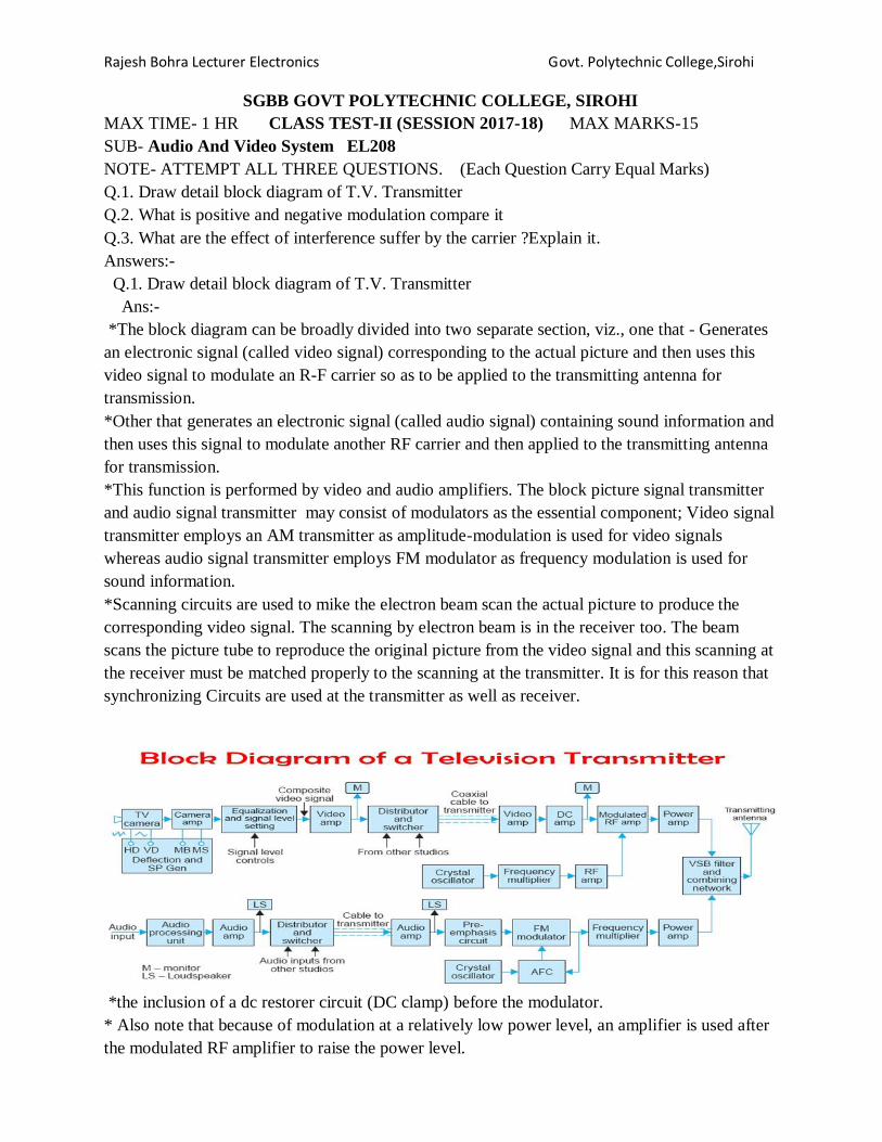
Q.1. Draw detail block diagram of T.V. Transmitter
Q.2. What is positive and negative modulation compare it
Q.3. What are the effect of interference suffer by the carrier ?Explain it.
Answers:-
Q.1. Draw detail block diagram of T.V. Transmitter
Ans:-
*The block diagram can be broadly divided into two separate section, viz., one that - Generates
an electronic signal (called video signal) corresponding to the actual picture and then uses this
video signal to modulate an R-F carrier so as to be applied to the transmitting antenna for
transmission.
*Other that generates an electronic signal (called audio signal) containing sound information and
then uses this signal to modulate another RF carrier and then applied to the transmitting antenna
for transmission.
*This function is performed by video and audio amplifiers. The block picture signal transmitter
and audio signal transmitter may consist of modulators as the essential component; Video signal
transmitter employs an AM transmitter as amplitude-modulation is used for video signals
whereas audio signal transmitter employs FM modulator as frequency modulation is used for
sound information.
*Scanning circuits are used to mike the electron beam scan the actual picture to produce the
corresponding video signal. The scanning by electron beam is in the receiver too. The beam
scans the picture tube to reproduce the original picture from the video signal and this scanning at
the receiver must be matched properly to the scanning at the transmitter. It is for this reason that
synchronizing Circuits are used at the transmitter as well as receiver.
*the inclusion of a dc restorer circuit (DC clamp) before the modulator.
* Also note that because of modulation at a relatively low power level, an amplifier is used after
the modulated RF amplifier to raise the power level.

Rajesh Bohra Lecturer Electronics Govt. Polytechnic College,Sirohi *Accordingly this amplifier must be a class-B push-pull linear RF amplifier. Both the modulator
and power amplifier sections of the transmitter employ specially designed VHF triodes for VHF
channels and klystrons in transmitters that operate in UHF channels.
Vestigial Sideband Filter
The modulated output is fed to a filter designed to filter out part of the lower sideband
frequencies.
Antenna
*The filter output feeds into a combining network where the output from the FM sound
transmitter is added to it. This network is designed in such a way that while combining, either
signal does not interfere with the working of the other transmitter.
*A coaxial cable connects the combined output to the antenna system mounted on a high tower
situated close to the transmitter. A turnstile antenna array is used to radiate equal power in all
directions. The antenna is mounted horizontally for better signal to noise ratio.
*Only one antenna is used for transmission of the video as well as audio signals. Thus these
modulated signals have to be combined together in some appropriate network. video as well as
audio signals have to be amplified to the desired degree before they modulate their respective RF
carriers.
Q.2. What is positive and negative modulation compare it.
Ans:-
*When the intensity of picture brightness causes increase in amplitude of the modulated
envelope,
it is called ‘positive’ modulation.
*When the polarity of modulating video signal is so chosen that sync tips lie at the 100 per cent
level of carrier amplitude and increasing brightness produces decrease in the modulation
envelope, it is called ‘negative modulation’
Comparison of Positive and Negative Modulation
(a) Effect of Noise Interference on Picture Signal:-
*Noise pulses created by automobile ignition systems are most troublesome.
* The RF energy contained in such pulses is spread more or less uniformly over a wide
frequency range and has a random distribution of phase and amplitude.
*When RF pulses are added to sidebands of the desired signal, and sum of signal and noise is
demodulated, the demodulated video signal contains pulses corresponding to RF noise
peaks,which extend principally in the direction of increasing envelope amplitude.
*Thus in negative system of modulation, noise pulse extends in black direction of the

Rajesh Bohra Lecturer Electronics Govt. Polytechnic College,Sirohi signal when they occur during the active scanning intervals.
*In the positive system, the noise extends in the direction of the white during active scanning.
*Obviously the effect of noise on the picture is less pronounced when negative modulation is
used.
*With positive modulation noise pulses will produce white blobs on the screen whereas in
negative modulation the noise pulses would tend to produce black spots which are less noticeable
against a grey background.
*This merit of lesser noise interference on picture information with negative modulation has led
to its use in most TV systems.
(b) Effect of Noise Interference on Synchronization:-
*Sync pulses with positive modulation being at a lesser level of the modulated carrier envelope
are not much affected by noise pulses.
*in the case of negatively modulated signal, it is sync pulses which exist at maximum carrier
amplitude, and the effect of interference is both to mutilate some of these, and toproduce lot of
spurious random pulses.
*Because of almost universal use of negative modulation, special horizontal stabilizing circuits
have been developed for use in receivers to overcome the adverse effect of noise on
synchronization.
(c) Peak Power Available from the Transmitter:-
*With positive modulation, signal corresponding to white has maximum carrier amplitude.
*The RF modulator cannot be driven harder to extract more power because the non-linear
distortion introduced would affect the amplitude scale of the picture signal and introduce
brightness distortion in very bright areas of the picture.
* In negative modulation, the transmitter may be over-modulated during the sync pulses without
adverse effects, since the non-linear distortion thereby introduced, does not very much affect the
shape of sync pulses.
* the negative polarity of modulation permits a large increase in peak power output and for a
given setup in the final transmitter stage the output increases by about 40%.
(d) Use of AGC (Automatic Gain Control) Circuits in the Receiver:-
* Most AGC circuits in receivers measure the peak level of the incoming carrier signal and
adjust the gain of the RF and IF amplifiers accordingly.
* In negative system of modulation, such a level is the peak of sync pulses which remains fixed
at 100 per cent of signal amplitude and is not affected by picture details.
*This level may be selected simply by passing the composite video signal through a peak
detector.
* In the positive system of modulation the corresponding stable level is zero amplitude at the
carrier and obviously zero is no reference, and it has no relation to the signal strength.
Q.3. What are the effect of interference suffer by the carrier ?Explain it.
Ans:-
*In addition to thermal and man-made noise, the carrier signal must compete with various other
forms of interfering signals originating from other television stations, radio transmitters,
industrial radiating devices and TV receivers.

Rajesh Bohra Lecturer Electronics Govt. Polytechnic College,Sirohi * When the interfering signal has a frequency that lies within the channel to which a TV receiver
is tuned, the extent of interference depends only on the relative field strengths of the desired
signal and the interfering signal.
*If the interfering signal frequency spectrum lies outside the desired channel, selectivity of the
receiver
aids in rejecting the interference.
(a) Co-channel Interference:-
*Two stations operating at the same carrier frequency, if located close by, will interfere with
each other.
*This phenomenon which is common in fringe areas is called co-channel interference.
*As the two signal strengths in any area almost equidistant from the two co-channel stations
become equal, a phenomenon known as ‘venetian-blind’ interference occurs.
*This takes the form of horizontal black and white bars, superimposed on the picture produced
by the tuned channel. These bars tend to move up or down on the screen.
* As the strength of the interfering signal increases, the bars become more prominent, until at a
signal-to-interference ratio of 45 db or so, the interference becomes intolerable. The horizontal
bars are a visible indication of the beat frequency between the two interfering carriers.
*Co-channel interference was a serious problem in early days of TV transmission, when the
channel allocation was confined to VHF band only.
*Now when a large number of channels in the UHF band are available such a problem does not
exist.
*co-channel interference can occur in fringe areas. The use of highly directional antennas is very
helpful in etiminating co-channel interference.
(b) Adjacent Channel Interference:-
*Stations located close by and occupying adjacent channels, present a different interference
problem.
*Adjacent channel interference may occur as a result of beats between any two of these
frequencies or between a carrier and any sidebands.
A coarse dot structure is produced on the screen if picture carrier of the desired channel beats
with sound carrier of the lower adjacent channel.
*The beat pattern is more pronounced if the lower adjacent sound carrier is relatively strong and
is not sufftciently attenuated in the receiver.
*To prevent adjacent channel interference, several sharply tuned band eliminator filters (trap
circuits) are provided in the IF section of the receiver.

Rajesh Bohra Lecturer Electronics Govt. Polytechnic College,Sirohi *the guard band between two adjacent channels also minimizes the intensity of any adjacent
channel interference. A space of about 150 km between adjacent channel stations is enough to
eliminate such an interference and is normally allowed.
(c) Ghost Interference:-
*Ghost interference arises as a result of discrete reflections of the signal from the surface of
buildings, bridges, hills, towers etc.
*Fig. shows paths of direct and reflected electromagnetic waves from the transmitter to the
receiver. Since reflected path is longer than the direct path, the reflected signal takes a longer
time to arrive at the receiver.
*The direct signal is usually stronger and assumes control of the synchronizing circuitry and so
the picture, due to the reflected signal that arrives late, appears displaced to the right.Such
displaced pictures are known as ‘trailing ghost’ pictures.
*On rare occasions, direct signal may be the weaker of the two and the receiver synchronization
is now controlled by the reflected signal. Then the ghost picture, now caused by direct signal,
appears displaced to the left and is known ‘as leading ghost’ picture.
*The effect of such reflected signals (ghost images) can be minimized by using directional
antennas and by locating them at suitable places on top of the buildings.

SGBB GOVT POLYTECHNIC COLLEGE, SIROHI
MAX TIME- 1 HR CLASS TEST-II (SESSION 2017-18) MAX MARKS-15
SUB- ELECTRONIC INSTRUMENTS (EL209) DATE-31/01/2018
NOTE- ATTEMPT ANY THREE QUESTIONS.
1) Explain Q-meter instrument.
2) Explain Harmonic distortion analyzer.
3) Write short note on any one of following: -
A) Megger
B) Spectrum Analyzer
MODEL ANSWERS
Answer 1:-
Q-Meter:-
The overall efficiency of coils and capacitors intended for RF applications is best
evaluated using the Q value. The Q Meter is an instrument designed to measure
some electrical properties of coils and capacitors. The principle of the Q meter is
based on series resonance; the voltage drop across the coil or capacitor is Q times
the applied voltage (where Q is the ratio of reactance to resistance, XL/R). If a
fixed voltage is applied to the circuit, a voltmeter across the capacitor can be
calibrated to read. Q directly..
For carrying out the measurement, the unknown coil is connected to the test
terminals of the instrument, and the circuit is tuned to resonance either by
varying the frequency of the oscillator or by varying the resonating capacitor C.
Readings of voltages across capacitor C and shunt resistance Rsh are obtained
and Q-factor of the coil is determined as follows :
By definition Q-factor of the coil,
Q = XL / R
And when the circuit is under resonance condition
XL = XC
Or IXL = IXC = VC
And the voltage applied to the circuit.
V = IR
So, Q = XL / R = IXL / R = VC / V
This Q-factor is called the circuit Q .
Answer 2:-
Harmonic distortion analyzers:
Harmonic distortion:
When we give a sinusoidal signal input to any electronic instrument there should
be output in sinusoidal form, but generally the output is not exactly the replica of
input, because of various types of distortion that my occur.
Distortion is occur due to inherent non-linear characteristics of different
components used in electronic circuit. Nonlinear behavior of electronic
component introduces harmonics in the output waveform and the resultant
distortion is often referred as harmonic distortion.
Types of harmonic distortion:
1) Frequency distortion:
This type of distortion occurs in amplifiers because of amplification factor of
amplifier is different for different frequencies.
2) Amplitude distortion:
It occurs because amplifier introduces harmonic of fundamental of input
frequency. Harmonics always generates distortion in amplitude. E.g. when
amplifiers are overdriven it clips the waveform.
3) Phase distortion:
This distortion occurs due to energy storage elements in the system which causes
the output signal to be displaced in phase with the input signal. Signals with
different frequencies will be shifted by different phase angles.
4) Inter modulation distortion:
This type of distortion occurs as a consequence of interaction or heterodyning of
two frequencies, giving an output which is sum or difference of the two original
frequencies.

5) Cross-over distortion:
This type of distortion occurs in push-pull amplifiers on account of incorrect boas
levels as shown in figure.
Total harmonic distortion (THD):
Harmonic Distortion Analyzer :-
Answer 3:-
(A) Megger :-
Insulation resistance IR quality of an electrical system degrades
with time, environment condition i.e. temperature, humidity, moisture and
dust particles. It also get impacted negatively due to the presence of
electrical and mechanical stress, so it’s become very necessary to check the
IR (Insulation resistance) of equipment at a constant regular interval to
avoid any measure fatal or electrical shock.
Uses of Megger:-

The device enable us to measure electrical leakage in wire, results are very
reliable as we shall be passing electric current through device while we are
testing. The equipment basically use for verifying the electrical insulation
level of any device such as motor, cable, generator winding, etc. This is a
very popular test being carried out since very long back. Not necessary it
shows us exact area of electrical puncture but shows the amount of leakage
current and level of moisture within electrical equipment/winding/system.
Electronic Type Megger :-
Important parts:-
Digital Display :- A digital display to show IR value in digital form.
Wire Leads :- Two nos of wire leads for connecting megger with electrical
external system to be tested.
Selection Switches :- Switches use to select electrical parameters ranges.
Indicators :- To indicates various parameters status i.e. On-Off. For Example
Power, hold, Warning, etc.
Note: - Above construction is not similar for every megger, it difference
appears manufacture to manufacture but basic construction and operation
are same for all.
Advantages of Electronic Type Megger
(I )Level of accuracy is very high.
(ii) IR value is digital type, easy to read.
(iii) One person can operate very easily.
(iv) Works perfectly even at very congested space.
(v) Very handy and safe to use.
Disadvantages of Electronic Type Megger
(i) Require an external source of energy to energies i.e. Dry cell.
(ii) Costlier in market.

(B) Spectrum Analyzer :-
A spectrum analyzer is a device that displays signal
amplitude (strength) as it varies by signal frequency. The frequency appears
on the horizontal axis, and the amplitude is displayed on the vertical axis.
To the casual observer, a spectrum analyzer looks like an oscilloscope, and
in fact, some devices can function either as oscilloscopes or spectrum
analyzers.
Fig. Block diagram of spectrum analyzer
The sawtooth generator provides the sawtooth voltage which drives the
horizontal axis element of CRT and this sawtooth voltage is frequency controlled
element of the voltage controlled oscillator (VCO). As the oscillator sweep from
𝑓𝑚𝑖𝑛 to 𝑓𝑚𝑎𝑥 of its frequency , it beats with the frequency component of input
signal and produce an IF (Intermidate frequency) . This IF is amplified and
detected and then applied to vertical plates of CRT and produce a display of
amplitude versus frequency .
Us e :- in the study of RF spectrum produced in microwave instruments.
S.G.B.B. GOVERNMERNT POLYTECHNIC COLLEGE SIROHI
SECOND CLASS TEST
Subject: C Language: CS201 dated 27.03.2018 / EL210 dated 26.03.2018
MM 15 Time 1Hour
Q1. Write difference between Array and Structure.
Q2. Write the advantages of using Pointer.
Q3. Write Short Note on:
& operator and
* operator
Ans 1.
Ans 2: Major advantages of pointers are:
(i) It allows management of structures which are allocated memory dynamically.
(ii) It allows passing of arrays and strings to functions more efficiently. (iii) It makes possible to pass address of structure instead of entire structure to the functions. (iv) It makes possible to return more than one value from the function.
Arrays Structures
1. An array is a collection of related data elements of the same type.
1. Structure can have elements of different types
2. An array is a derived data type 2. A structure is a programmer-defined data type
3. Any array behaves like a built-in data types. All we have to do is to declare an array variable and use
it.
3. But in the case of structure, first, we have to design and declare a
data structure before the variable of that type are declared and used.
4. Array allocates static memory and uses index/subscript for
accessing elements of the array.
4. Structures allocate dynamic memory and uses (.) operator for
accessing the member of a structure.
5. An array is a pointer to the first element of it
5. Structure is not a pointer
6. Element access takes relatively less time.
6. Property access takes relatively large time.

Ans 3: Address of (&) Operator in C
This operator returns address of any variable.
Consider the given example
#include <stdio.h>
int main()
{
int x=10;
printf("Value of x: %d\n",x);
printf("Address of x: %X\n",&x);
return 0;
}
Output
Value of x: 10
Address of x: F0C10E3C
Unary plus (+) Operator
This operator does not make any effect on the operand value, it just returns
operands value.
Consider the given example:
#include <stdio.h>
int main()
{
int x= +4;
printf("x= %d\n",x);
return 0;
}

Output
x= 4
Here, we assigned +4 to the variable x and the result is 4.
2) Unary minus (-) Operator
This operator makes the value negative. It makes positive value to negative and
negative value to positive.
Consider the given example:
#include <stdio.h>
int main()
{
int x=10;
int y=-20;
printf("value of -x: %d\n",-x);
printf("value of -y: %d\n",-y);
return 0;
}
Output
value of -x: -10
value of -y: 20
Here, we assigned 10 to variable x and -20 to variable y, when we print the value of
both variables using Unary minus operator, the result is -x= 10 and -y= 20.