The PCB Magazine, September 2014
83
-
Upload
khangminh22 -
Category
Documents
-
view
2 -
download
0
Transcript of The PCB Magazine, September 2014


Electrochemical corrosion, dendritic growth, conductive anodic filaments, BGA cracking and lead-free solder joint thermo-mechanical fatigue can all have negative impacts on the reliability and performance of today’s high technology electronics.
IPC Europe High Reliability Forum, a two-day conference co-developed by top organizations including: Airbus, Celestica, COM DEV, Continental Automotive, The European Space Agency, Gen3 Systems, The National Physical Laboratory, Robert Bosch, Thales and Zestron will bring together leading experts from industry and research institutions to explore these critical reliability issues and more facing European electronics designers and manufacturers.
IPC Europe High Reliability Forum 14–15 October, 2014 | Düsseldorf, Germanywww.ipc.org/eu-high-reliability
REGISTER NOW
Media Supporter:

4 The PCB Magazine • September 2014
18
30
Aluminum Base Circuit Technology: Structures & Manufacturing Methodsby Joseph Fjelstad
3D LDS Components:New Opportunities in PCB Layout and Productionby Malte Borges
Aerosol Jet Technology for Production Grade/Scale Printed Electronicsby Ken Vartanian
feature ColumnsThe Family (Sun)Stoneby Ray Rasmussen
Making the Impossible Possibleby Judy Warner
se
pt
em
be
r f
ea
tu
re
d C
on
te
nt
42
8
52
this month, industry experts from Verdant electronics, lpKf, optomec and transline tech-nology explore up and coming technologies for pCb fabrication, layout and more.
New Concepts and Emerging Technologies
for PCB Fabrication


6 The PCB Magazine • September 2014
Video interViewsAdvanced West Acquires DryerManufacturer Comac
OEM Press Systems Has New CEO,New Technology
shorts3D Printers Create Custom Medical Implants
Researchers Develop TransparentSolar Concentrator
news highlightsSupplier/New Product
Mil/Aero007
Markets
Top Ten PCB007 News Highlights
reader responseAnd the Data Transfer Beat Goes On...from Karel Tavernier
ColumnsWhere do we go From Here?by Todd Kolmodin
Root Cause of Failures in PWB Laminationby Michael Carano
Best Practices 101, Part 2by Steve Williams
extrasEvents Calendar
Advertisers Index & Masthead
Co
nt
en
ts
New
Concepts and Em
erging Technologies for PCB Fabrication
60
66
72
76
82
83
50
57
40
75
58
64
70
80
september 2014
Volume 4
Number 9
the defiNitiVe
iNteractiVe magaziNe
dedicated to the
global pcb iNdustry
thepcbmagazine.com


8 The PCB Magazine • September 2014
by Ray RasmussenI-ConneCt007
During the IPC APEX EXPO show in Las Ve-gas, I had the chance to meet with Terry Heil-man and Rocky Catt, owners of Sunstone Cir-cuits. They wanted to introduce me to their new marketing manager, Matt Stevenson.
During the discussion, we talked about their company and what they believe is their unique style of doing business. Although I understood much of what they were trying to convey, Heil-man suggested I make a trip to their factory to see for myself. I’d have to experience what they were doing to get the complete story. He was right. There was much more to the story.
By the way, the title for this article came to me early on while touring their factory and stuck in my head throughout the day and as I started to put this article together. I think you’ll see why.
The CompanySunstone Circuits is tucked neatly into a
small valley in a rural community about an hour south of Portland, Oregon. Employing about 150 people, this nondescript factory, a kludge of rooms in a building constructed and modi-fied many times over the last 50 years, pumps
the way i see it
fe
at
ur
e C
ol
um
n
The Family (Sun)stone
figure 1: front row, l-r: terry Heilman, Sheri Kuretich, rocky Catt, nolan Johnson, nancy Viter. Back row, l-r: molly o’Hara, les Stephens, Paul Waterman, matt Stevenson, al Secchi.

Can you imagine CAM to etch in 5 minutes?Meet Lunaris, the first fully digital inner
layer printer based on inkjet technology.
Click here to meet
Simplified Inner layer production flow with Lunaris
Inner layer production methods haven’t changed much in over forty years. The basic process has remained the same: use lots of interdependent equipment and chemistry to completely cover a panel with photo resist. Then, use some more interdependent equipment and chemistry to remove most of it!
This is a timely, wasteful and costly process.Lunaris has a better way:
Our revolutionary technology eliminates over 70% of the processes prior to inner layer AOI, reducing the time from hours or days to just minutes!
www.mutracx.com
CAM Clean Etch
StripAOI

10 The PCB Magazine • September 2014
out about 200–250 quick-turn, prototype PCB orders each day to meet the needs of custom-ers, predominately in the U.S. Like clockwork, orders flow into their highly automated website and frontend systems, and 24–72 hours later (mostly, depending on board configurations) flow out the back door of the shipping depart-ment.
Although a small manufacturing footprint, it’s really easy to get turned around as you walk from room to room following a somewhat logi-cal manufacturing flow. It’s also easy to under-estimate their capabilities. They do a lot with what they have to work with. The factory has had to grow up inside a less-than-desirable, seri-ously constrained environment. If asked, Sun-stone managers will tell you that the company occupies 40,000 square feet, but that includes a brand new 8,000 square-foot office building which houses most of the management, cus-tomer service, inside sales, marketing and most admin functions. The rest is where they make PCBs, 24/7, almost 365 days of the year. It’s not necessarily an elegant dance, but there is style, form, function and friendliness to it.
The DanceYears ago I had the chance to visit high-tech
proto maker DDi. At DDi, there wasn’t any fi-nesse. They muscled out high-tech protos to all comers at astronomical prices. It was a model that really worked for them. DDi had lots of technical capabilities and the people with the expertise to push the boards through the factory to capture the ridiculous amounts that Silicon Valley engineers were willing to pay to prove out a product design. As was pointed out to me, they were selling time, not just PCBs. I suggest-ed to the management that some systems work might really help them lessen the chaos, accel-erate the manufacturing flow and make more money. You had to admire what they did back then, but they could have done so much more and been so much better.
Sunstone is better. They don’t tackle the technology the way DDi did, but they have cer-tainly embraced systems thinking. Boards flow through the factory at lightning speed, but it’s more of a dance as opposed to a monster truck rally. It’s not a rushed or hectic environment,
but a nice, smooth flow. How often do you see harmony in a board shop?
The FamilyHere’s where I came up with the article title.
During my span of 25 years covering the indus-try, I’ve heard lots of companies talk about their people in glowing terms: “we’re like family,” or “our people come first,” or “it’s all about the people.” The majority of the time, those state-ments don’t have much substance. You’ll hear comments like that when a company embarks down some type of continuous improvement path. It’s one of the first things managers start talking about, but it’s also the first thing they drop when the going gets tough. With Sun-stone, although they, too, have embarked on a continuous improvement path, the family (the people) genuinely does seem to come first. And I literally mean family: sons and daughters work-ing with their parents who’ve been with the company for decades or spouses with long, col-lective histories with the company. Still, there is a company-wide esprit de corps fostered by the leadership. I’m sure it’s not all roses, but there seems to be a genuine, top-down commitment to the well-being of the entire Sunstone family.
That commitment to the employees ulti-mately takes care of the customer. It’s W. Ed-wards Deming’s teachings without the Dem-ing. Heilman and Catt say it just makes sense. It makes for a great place to work, builds em-ployee loyalty and translates into a better expe-
THE FAMILy (SuN)STONE continues

September 2014 • The PCB Magazine 11
rience for the customers. I heard that about a dozen times from their team of managers and from those working on the factory floor: “Does it benefit the customer?” was their mantra.
Almost unique Sales ModelSunstone has an interesting method of gen-
erating sales, which isn’t entirely unique. Other companies follow a similar system but I doubt to this extent. The company markets heavily on the Internet, casting a wide net, moving pro-spective customers into the automated sales sys-tem built into their website. Orders are placed there and files are uploaded, and it’s all done pretty much without human contact. According to Heilman, their goal is to bring in 15–20 new customer orders each working day. That’s some-where around 300–400 new customers each month, on top of the 4,000 or so orders they process from existing customers. To give you some perspective, with an average order value of around $500, you can work out some rough an-nual sales revenue numbers, which likely places them in the range of $20–30 million annual revenue. Having already attracted over 30,000 customers, I had to ask how many more pros-pects Sunstone thinks are out there. After all, it’s a finite market. You can’t reach 15–20 new customers a day forever. They felt comfortable with their strategy and thought that the goal could continue to be achieved for some time to come. Of course, they continue to nurture their current base of customers looking to grow that business, as well. My take is that they’ll have to begin offering leading-edge technology capabil-ities to attract more business at some point.
Industry veteran Harvey Miller, owner of the PCB directory Fabfileonline, reports the size of the North American market to be about $1.2 billion for prototype PCBs annually. Heilman thinks that number is closer to $350 million for rigid board prototypes. In either case, Sunstone has room to grow.
The Sunstone model does sound attractive, though. They have a wide, diverse customer base (10,000 of the 30,000 placed orders over the last year), which builds in some security. Ap-proximately 50% of Sunstone’s customers pro-vide about 75% of their revenue, which means they must do a great job of keeping customers;
combined with the new ones coming in every day, it makes for good, predictable growth.
Another interesting fact about this sales model is that about 80% of their orders are paid by credit card, which partially explains why their bad debt only amounted to $3,000 over the last year. Other contributing factors are the various other benefits to their credit card model, such as increased cash flow, security of payment, etc. But there is a cost associated with this model, which does detract from the bottom-line ben-efit. Nonetheless, when you look at their cost of sales, cost of manufacturing, overhead, lack of debt service and, now, virtually no bad debt, they pick up a couple of points in all these areas. Overall it’s a simple and effective model.
Customer is Always RightThis is easier said than done. At I-Con-
nect007, we love our customers and tend to side with them when things go awry, but they aren’t always right. Sunstone tends to walk the walk that no matter what happens, it needs to ben-efit the customer. I don’t think this was a show put on just for my benefit. I heard it too many times, in too many places, from a lot of differ-ent people at Sunstone. They genuinely want to care for their customers. Everything they do must be of benefit to the customer. Again, Deming says it a little differently: Care first for employees, which Sunstone appears to do (see “The Family” above) and they will take care of the customer. Regardless of the order of things in Sunstone’s thinking, it is what’s happening: Everyone’s needs are being met.
Philosophy The owners claim that Sunstone is quite
profitable, and they’ll continue to work to drive waste out of their systems, which translates into additional profitability and more capacity, and in turn, increased benefits to customers. I get this, and I am quite surprised at how few com-panies pursue excellence in manufacturing and in business. It’s a no-brainer for me.
Since 2005, when Heilman and Catt pur-chased the company from Electronic Controls Design (ECD), they’ve been able to pay off the previous owner and continue to upgrade capa-bilities while staying out of debt. Even the new
THE FAMILy (SuN)STONE continues

12 The PCB Magazine • September 2014
facility they built was paid for with cash. Accord-ing to Heilman, being debt-free is by no means a mandate, but instead, a result of budgeting capital equipment and facility upgrades yearly in order to maintain a financially responsible model. That discipline has placed them in the catbird seat as they survey the industry for ad-ditional opportunities. They’re certain that their business model will work in other PCB factories or in other industries, as well, and in turn, value the customer.
AlliancesSunstone has a partnership with Scream-
ing Circuits, an EMS partner that handles any assembly work that comes in. Located just 12 miles from Sunstone, Screaming Circuits, like Sunstone, is truly customer-focused, and their relationship is “very synergetic,” says Heilman. When asked about vertically expanding their services, they were quite comfortable with their assembly partner as this point. While they do offer layout services for their customers, they are not in the design business.
The TechnologySunstone does not pretend to build leading-
edge PCBs, either; it’s not their model. What they do is reliably deliver 2-, 4-, 6- or 8-layer, 5/5 mil lines and spaces boards, quickly, complete and on time, guaranteed. They can do up to 20 layers and tighter lines, but it’s not their sweet spot. I do see a pretty compelling opportunity to climb the technology ladder a bit, which could open the door to more customers or significant-ly expand the volume of business they do with their current customers.
Their business model does not focus on per-formance certifications, and as such, they aren’t certified for mil/aero or medical, but I did notice an ITAR registration from a 2012 press release. They say their customers just don’t need those certifications to prove out a circuit, and that the amount of business they lose doesn’t justify the expense of qualifying and maintaining the certi-fications—not for the kind of work they do.
Manufacturing ChallengeRunning at about 75% capacity, there is
room to grow, but the facility is currently maxed
in size due to land zoning restrictions. That size restriction is somewhat limiting and is requir-ing them to look at new equipment which can produce more product within the existing foot-print. The good news is that many of the new systems do just that. And, as long as they’re as profitable as they say they are, buying the equip-ment necessary to add another 20–50% capac-ity is very doable. In addition, just about every-thing they buy will give Sunstone higher-tech capabilities, which could help them move up in technology offerings.
Small BatchesOptimized processes designed to utilize
equipment efficiently translates into five or six 14”x16” panels making up the normal lot size running through the factory. Because of that, you see equipment sized to fit that manufacturing model. Panel utilization is maximized as like jobs are aggregated or nested with other like boards, while increasing throughput to keep costs down for the customer. I do believe Sunstone has an opportunity to accelerate their manufacturing even more, but that would probably require ad-ditional equipment and more factory floor space. But right now, if customers order a conforming PCB by 4 p.m. PST, they can be assured that their order will ship the next afternoon.
In their shipping department, a five-foot high stack of FedEx and UPS boxes are staged and ready to meet the day’s orders. What looks like a frenzy really isn’t one at all. It’s a well-oiled machine driven by tight systems and highly dedicated employees, although the department tends to get a bit harried as shipping times ap-proach, I was told. But most jobs fit nicely in the shipping boxes provided, which simplifies and speeds up the shipping process.
RedundancyQuite honestly, redundancy was the weak
link for me. Because of their factory size con-straints, they aren’t able to add a lot of redun-dancy to their systems. Also, their location, although it’s probably a great place to live, is somewhat isolated. However, according to Heil-man, that’s where the years of experience come in. And as Nancy Viter, director of manufac-turing explained, when their photo processor
THE FAMILy (SuN)STONE continues


14 The PCB Magazine • September 2014
went down recently, instead of panicking, they switched back to trays of solution to process the film, the way they used to do it. They do the same when other processes fail. They know how it was done in the old days, so they adjust until they get things running again. They do have co-op agreements with a few fabricators in the area, which can help in a crisis. And operating 24/7 gives them the opportunity to fix a process and catch up during the next shift. Maintenance people are available at any hour of the day to ensure things keep humming.
Equipment upgradesAlthough the operations are well-controlled
and thought out, the company can benefit greatly from some newer equipment. There are a few new purchases in the wings, which Viter discussed while we were touring the fac-tory. They’re looking at a new two-spindle drill machine and a direct imaging system, both of which are designed to increase throughput and improve capabilities. I’m sure these new systems will also help maximize the factory production footprint. There’s also an OEM press on order that happens to be the only one small enough to fit in the space of the old press, and they’re continuing to upgrade as it makes sense.
As I mentioned earlier, Sunstone’s commit-ment to remaining profitable has driven their efforts to maximize usage of existing equipment and processes. They prefer to make smaller, budgeted, methodical moves when it comes to capital equipment. They don’t have to climb the technology ladder too quickly to meet the needs
of most of their customers for 5/5 technology. Instead, their focus is on speed and customer service. How can they move boards more quick-ly through the factory and out the back door to the customer?
Management ExperienceAs I talked with the management team and
factory floor employees, names like Tektronix, Merix, Praegitzer and Viasystems, popped up. It seems that Sunstone has been the beneficiary of the talent of a few of its neighbors and bygone shops. The rest of the company employees have been homegrown over the last decade or two. More on Sunstone’s managers in the sidebar.
The GuaranteePutting their money where their mouth is,
they’ve upped the ante by attaching a guaran-tee. If they don’t “deliver quality boards, on time with the right quantities,” then the order is free.
I think if most of us realized we were going to be late, we would prefer to work with cus-tomers to see if they were OK with the delay or to see if we could make partial shipments, etc. We wouldn’t discount our work unless we had to. In fact, most customers would probably be fine with a delay, here and there, as long was the communication was good. They’re kind of used to that.
When the idea of a guarantee was first floated at Sunstone, some thought it was a bit too much. But after a review of their delivery history, they decided to make that offer and stand behind it. They have had to eat a few orders since they first instituted the program, but the process improve-ments they’ve made as a result have benefitted the company way beyond the cost. They’ve had to step things up but it’s been a win for the com-pany and a win for the customers.
Although I might have ruffled a few feath-ers among senior managers when I called the guarantee a gimmick, I did follow that up by saying that offering a guarantee does three things. It gets people’s attention, it demon-strates confidence, and it helps ensure custom-er loyalty. The gimmick is what we see on the outside, but the systems and people behind it, as well as the effect is has on the customer, are the real thing.
THE FAMILy (SuN)STONE continues

atg Luther & Maelzer GmbHZum Schlag 3 • 97877 Wertheim • GermanyPhone +49-9342-291-0 • Fax +49-9342-395 [email protected] • www.atg-lm.com
Basic specification
Test area
Smallest test point
Repeatable accuracy
Test voltage
4-wire Kelvin measurement
16 test probes, 8 XGA color cameras
610 mm x 620 mm
25 µm (*with micro needle probes)
+/- 4 µm
up to 1000 Volts
0,25 mΩΩ - 1 kΩ (± 0,1 mΩΩ ± 2
Introducing the atg A8-16 with 16 test probes,8 XGA color cameras, and an unrivaled test speed
of up to 275 measurements per second.
A8-16 Video Get more info
Unrivaled Speed.

16 The PCB Magazine • September 2014
THE FAMILy (SuN)STONE continues
The Sunstone Teamin the words of director of manufacturing
nancy Viter:
at sunstone, the philosophy of empowerment is more than just a catch phrase. each team mem-ber is a leader in his own way, and understands that the responsibility to give the customer the best ex-perience possible falls squarely on each individual’s shoulders. the beauty of this way of thinking is that there is very little finger-pointing when prob-lems arise. team members are expected to con-tribute to the solution, regardless of the challenge. if a piece of equipment goes down in the middle of the night, waiting until morning when a lead-er arrives is not an option. this builds teamwork, as all available resources come together to share manpower and knowledge. are there teachable moments that might result in a well-meaning, but perhaps unsuccessful solution? absolutely!
but individuals know that making a decision is better than doing nothing at all, and with all the years of experience and successful problem solving to call on, the risk of this empowerment philoso-phy is minimal. from the head of the organization all the way to the newest, youngest staff member, sunstone leads by example, whether there is a title attached to the name or not, and this concept is taught in word and deed as new hires are trained.
all that said, here is a snapshot of some em-ployees who contribute to our success daily:
Rocky Catt (41 years), co-owner: with 30+ years of experience, rocky has served as a line supervi-sor, general manager and is the vice president and Coo of sunstone Circuits, where he oversees the company’s operations.
Terry Heilman (16 years), co-owner: terry over-sees all corporate operations, strategic marketing and financial planning for the company, and sun-stone’s significant growth reflects heilman’s guid-ance and contribution to providing the most ex-treme customer experience in the industry.
What I liked most about the guarantee is the opportunity it provides Sunstone to improve the process. I remember when Mo-torola went to Six Sigma (zero defects) as the quality standard to strive for back in the 1980s. They realized that if they chose the more attainable goal of Three Sigma they could continue to do the same things just a little better. With Six Sigma they’d have to change everything. It caused a revolution in their manufacturing. In my mind, the guar-antee is that kind of an effort, and it would cause many in the industry to have to re-invent their companies. Still, many compa-nies will tell you that they’re 100% on time but when you really look at the data, that isn’t the case. There are lots of exceptions used when calculating that number. The Sunstone guarantee, from what I gathered, is that they honor the guarantee regardless of the situation without input from the cus-tomer. If they don’t do what they say, they pay. As a result, over 50% of the customers who’ve received free boards are pleasantly surprised.
Open all yearThat’s another differentiator the compa-
ny uses to expound on their customer ser-vice. They are always open, and available to take customer calls. Heilman was unapolo-getic when we talked about the commitment behind this next level of service. “Why not? Why wouldn’t we offer this to our custom-ers? Shouldn’t they be able to talk to some-body whenever they want? If it’s important to them to know the status of their boards or to try and solve a problem on New Year’s Eve, shouldn’t it be important to us, as well?”
The SqueezeSince I’m not a maker of prototypes,
I haven’t been noticing the effect that im-provements in PCB design software has had on this segment. It seems that the software is getting pretty good. In fact, as Viter point-ed out, they’re seeing fewer and fewer PCB revisions. Customers are now able to prove out designs in software, pretty much, which leads to fewer prototype orders.

September 2014 • The PCB Magazine 17
The Family (Sun)STone continues
The Sunstone Team (Continues)
• Sheri Kuretich (21 years), human resources Ed Graham (38 years), safety and environmental• Bill Moffatt (28 years), maintenance Lynda Postlethwaite (30 years), sales and customer service• Joe Phelps (16 years), automation programming/ Cam support• Wayne Austin (31 years), Cam• Tammy Russell (27 years), mechanical operations• Donna Miller and Cindy Marshall (64 years combined), line• Bill and Sue McDowell (50+ years combined), imaging and plating• Jake Taylor (11 years) and Mike Hebda (12 years) • Karen Brugger (23 years), quality• Carrie Adams (30 years), (lPI) • Albert Wolf (36 years), (lPI) • Trina Taylor (16 years), imaging• Doug Miller (7 years), shipping• Mike Connella (7 years), Jeff Loewen (7 years), Tom Hall (10 years), Carrie Ditton (8 years), and Dennis Hammer (<1 year) • Kelly Atay (10 years), administration • Teresa Burtis (17 Years), administration• Mike Butler (5 Years), It• Sal Hernandez (8 years), customer support • Matt Rhodes (4 years), customer support
and then there is me, Nancy Viter. I consider myself more of a cheerleader, although I could be considered a director of a beautiful orchestra that is made up of the entire Sunstone team. each in-dividual is like a finely-tuned instrument, and we make beautiful music together. everyone knows his part, plays it dependably, and the unique Sun-stone symphony would be difficult, if not impos-sible, to copy. We play for a very special audi-ence: our customers and one another.
Better design software, emerging tech-nologies like printed electronics and other engineering prototyping systems will con-tinue to pressure the company in the com-ing years. But that’s where Heilman and Catt come in.
The FutureThe partners are keeping their eyes open
for opportunities to grow and expand their business. Landlocked in their current facil-ity, any substantial growth will require an additional facility, an idea which is on the table. Neither Heilman nor Catt are in a hurry to grow, but when they do, they will likely do it carefully and methodically—not just for the sake of growth. Heilman’s exten-sive background with M&As and business management should help them avoid many of the pitfalls associated with mismatches so common in typical M&As. Expansion, acquisitions, adding value to the services they already provide to their thousands of customers in the PCB industry are all on the table. They are very profitable, debt free, growing and having fun. It would seem to me that Sunstone is ready to make a care-fully calculated next move. PCB

18 The PCB Magazine • September 2014
by Joseph FjelstadVerdant eleCtroniCs
fe
at
ur
e
AbstractAluminum is an attractive material for use
in the manufacturing of electronic assemblies, owing to its low cost, good thermal properties, dimensional stability, environmental friendli-ness and ubiquity. Unfortunately, due to its in-nate thermal spreading ability, it is not easily used when solder is required to make intercon-nections to components. This article describes ways to manufacture electronic assemblies us-ing aluminum as a base and eschewing the use of solder.
Introduction RoHS restrictions on the materials used in
electronics manufacture have imparted sig-nificant challenges on the electronics industry since their introduction in 2006. The greatest impacts have been felt by the mandated elimi-nation of lead from electronic solder, followed by the demand for the elimination of haloids from flame retardants used in traditional PCB
laminates. Since 2006, the electronics industry has been beset with a host of new challenges in its effort to comply. Failure mechanisms, both new and old, have surfaced which demand so-lution and the industry suppliers and manufac-turing technologists have worked diligently to remedy those vexing faults through the devel-opment of a wide range of new materials and equipment for both board manufacture and assembly, along with modifications to the pro-cesses used in the manufacture and assembly of printed circuit boards.
Most of the problems which have con-fronted the electronics manufacturing indus-try have related to the solder assembly process. Lead-free solders were advertised early on as a drop-in replacement for traditional tin lead sol-ders; however, field experience proved it not to be the case. The tin-rich alloys, along with the higher temperatures required for assembly, cause the industry to scramble for solutions to such problems as champagne voids, poorer wet-ting, brittle solder joints, copper dissolution, tin whiskers, head-in-pillow, greater vulnerabil-ity to damage caused by explosive outgassing of absorb moisture in packages among others
UYEMURA USAwww.uyemura.com
ULTIMATE ADHESION
EXCEPTIONAL FLEXIBILITY
Corporate Headquarters: Ontario, CA • ph: (909) 466-5635 • (800) 969-4842 • fax: (909) 466-5177 Tech Center: Southington, CT • ph: (860) 793-4011 • (800) 243-3564 • fax: (860) 793-4020
OPTIMUM TOPOGRAPHY
MEC UICFROM
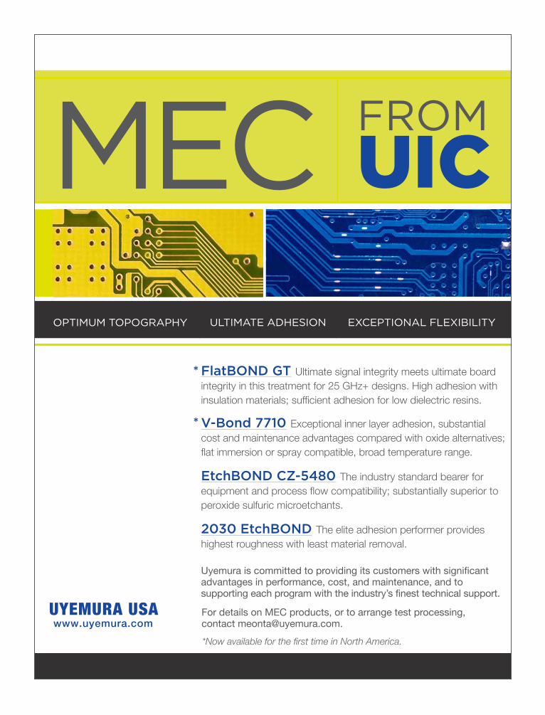
V-Bond 7710 Exceptional inner layer adhesion, substantial cost and maintenance advantages compared with oxide alternatives; flat immersion or spray compatible, broad temperature range. EtchBOND CZ-5480 The industry standard bearer for equipment and process flow compatibility; substantially superior to peroxide sulfuric microetchants. 2030 EtchBOND The elite adhesion performer provides highest roughness with least material removal.
FlatBOND GT Ultimate signal integrity meets ultimate board integrity in this treatment for 25 GHz+ designs. High adhesion with insulation materials; sufficient adhesion for low dielectric resins.
Uyemura is committed to providing its customers with significant advantages in performance, cost, and maintenance, and to supporting each program with the industry’s finest technical support. For details on MEC products, or to arrange test processing, contact [email protected].
*
*
*Now available for the first time in North America.

20 The PCB Magazine • September 2014
the surface of the aluminum. In subsequent processing the aluminum component board is first coated with an insulating material and then circuits which interconnect the compo-nents are applied using buildup technologies. An example of a solderless test vehicle assembly is shown in Figure 1.
The balance of this article will describe in more detail the processes used in the manufac-ture of such product and enumerate the numer-ous benefits that can be derived by simply re-versing the manufacturing process. That is plac-ing circuits on component boards rather than components on circuit boards.
Basis Manufacturing Concept
A new process for manufacturing a PCB which is comprised primarily of aluminum is hereafter described. The novel process bypasses completely the soldering process in accordance with the precepts consistent with what is known as the Occam process[1,2]. The Occam process is a subset of technologies that fall under the gen-eral umbrella term of SAFE an acronym which stands for either “solderless assembly for elec-tronics” or “solder alloy-free electronics.” SAFE manufacturing is relatively simple compared to traditional circuits, and the cost should prove significantly lower.
In brief, the process is carried out by plac-ing electrically tested and burned-in electronic components onto an aluminum carrier plate/housing. This can be performed using tradi-tional pick and place equipment. The resulting structure is fundamentally a component board. Following secure placement of the components, processing methods traditionally used for the manufacture of HDI buildup boards are carried out on the surface of the component bearing aluminum assembly to produce circuit patterns with the interconnection between components and circuit pattern being effected by copper plating of both the circuit features and the vias which interconnect component leads to those circuit features at desired locations. One advan-tage of note at this point is that unlike soldered devices, only those component leads requiring connection need be provided with vias. In ad-dition, the vias are smaller than the traditional solder lands so more surface area is available for
including cleaning of baked on fluxes follow-ing the high temperature assembly process. Lead-free solder also had spillover effects on the PCB laminate material itself as manufacturers experienced delamination and degradation of the resins used in traditional circuit construc-tion. One more recently encountered problem is a phenomenon referred to as pad cratering, wherein resin beneath the copper land to which a component is attached is actually torn loose from the surrounding resin breaking through the copper and causing an open.
In this environment, an alternative ap-proach to manufacturing electronic assemblies has been conceived and is presently being de-veloped. The new method in simplest form is one which eschews the use of solder and is predicated on the use of aluminum substrates which house fully tested and burned in com-ponents to create what can be best described as a component board wherein the terminations of the components are proximately planar with
ALuMINuM BASE CIRCuIT TECHNOLOGy continues
figure 1: aluminum is a viable alternative to customarily used laminates when solder is not used to make interconnections between compo-nents and circuits. aluminum is unique in that its surface can be anodized, creating an insula-tion layer of alumina which can be colored and sealed. all components shown have a purposely selected 0.5mm contact pitch for reasons discussed in the text.
September 2014 • The PCB Magazine 21
circuit routing. This will be discussed again later in the paper.
Aluminum is an attractive choice as a circuit substrate owing to a combination of different properties, which include a coefficient of ther-mal expansion reasonably proximate to that of copper, dimensional stability which exceeds that of FR-4, relative light weight, good thermal spreading capability, and low cost (aluminum is roughly $2 per kilogram, while FR-4 in quan-tities of 2,000 kilograms coming out of China runs around $6 per kilogram[3]). It is also worth noting that aluminum comprises 8.3% of the earth’s crust and is highly recyclable position-ing it among the most sustainable of all circuit substrate choices.
Turning attention back to the steps in the process, a sheet of aluminum is prepared with cavities wherein components will be placed. Be-cause the substrate is solid metal, the cavities can be created by any of a number of steps in-cluding chemical machining, mechanical ma-
chining, laser cutting and punching. The sub-strate could also be embossed or cast with the cavities if desired.
Aluminum is a unique metal that can be an-odized, converting the surface to aluminum ox-ide, also referred to as alumina. As a conductive material, aluminum can also be coated electro-phoretically with a plateable insulating mate-rial, making the surfaces nonconductive. Such techniques are commonly used in the coating of a wide range of metals used in products of every imaginable type from toys and household appliances to automobiles and space craft.
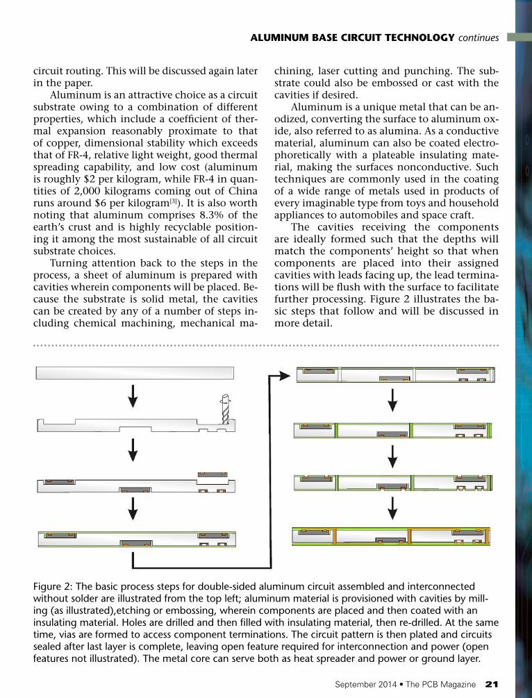
The cavities receiving the components are ideally formed such that the depths will match the components’ height so that when components are placed into their assigned cavities with leads facing up, the lead termina-tions will be flush with the surface to facilitate further processing. Figure 2 illustrates the ba-sic steps that follow and will be discussed in more detail.
ALuMINuM BASE CIRCuIT TECHNOLOGy continues
figure 2: the basic process steps for double-sided aluminum circuit assembled and interconnected without solder are illustrated from the top left; aluminum material is provisioned with cavities by mill-ing (as illustrated),etching or embossing, wherein components are placed and then coated with an insulating material. holes are drilled and then filled with insulating material, then re-drilled. at the same time, vias are formed to access component terminations. the circuit pattern is then plated and circuits sealed after last layer is complete, leaving open feature required for interconnection and power (open features not illustrated). the metal core can serve both as heat spreader and power or ground layer.

22 The PCB Magazine • September 2014
While the use of bare die is possible, the IC components to be used are ideally packaged (CSPs are very well suited) because packaged IC devices are much more easily tested and burned in and because they have standardized lead pat-terns and physical outlines making the design process simpler, especially if a single lead pitch is used for all components (e.g., 0.5 mm). Ad-ditionally, nearly all packaged components use copper as the base metal for interconnections, which is advantageous for more than just that one reason alone, as will be shown.
After the components are affixed permanently on one or both sides of the aluminum carrier plate, layers of insula-tion are applied to one or both surfaces of the metal sheet covering the components. At this point, the assembly can be processed as if it were a standard rigid printed circuit with high density build-up layers on one or both sides, us-ing lasers to drill holes down to access component termina-tions and commonly practiced plating and imaging processes to create the circuits. A dif-ference is that a fill step with an insulating material may be required if through-holes have exposed metal. However, if coated with epoxy, this may not be necessary. One caveat for those circuit manufacturers consid-ering exploring processing circuits of this type is that if the aluminum is untreated, the edges need to be sealed to prevent contamination of subsequent processing chemistries that will be used in manufacture. While additional process-ing steps can be performed if desired and or re-quired, this assembly could be in some applica-tions considered complete. The overall number of processing steps is obviously significantly reduced from those required for traditional pro-cessing of printed circuit assemblies.
While the foregoing has described a relative-ly simple structure the longer-range potential of
these novel aluminum circuit structures is im-pressive and limited more in my imagination than the technology. One such example is il-lustrated in Figure 3.
Advantages of Aluminum Circuit Assemblies
Beyond the structures just described, there are a striking number of advantages to the de-sign and manufacture of electronic assemblies
that do not use solder to make in-terconnections, especially those
made with aluminum. How-ever, the advantages of prod-ucts manufactured using SAFE techniques also circumscribe the full range of benefits nor-mally considered desirable for any electrical or electronic product. Following are brief discussions of those benefits:
A. Economic Benefits In a highly cost-competi-
tive global economy, the cost of manufacturing is always a high order concern. Looking first at material, the reader is asked to note again that the primary material of interest in this discussion has been aluminum. Aluminum is the third most abundant material on our planet (oxygen and sili-
con are first and second, respec-tively). As was mentioned earlier,
it comprises 8.3% of the earth’s crust. Because of its commodity status, aluminum is sold by weight regardless of thickness and it is less expensive per unit volume than com-posite materials. Though aluminum is admit-tedly denser than FR-4 laminate (2.8 g/and in cm3 aluminum versus 1.8 g/cm3 for FR-4), the amount of aluminum required can be very cost competitive in the long run. In contrast, the price of polymers varies due to the volatility of the price of oil, so there are advantages to being able to use a material such as aluminum, the price of which is reasonably predictable because of its global abundance.
ALuMINuM BASE CIRCuIT TECHNOLOGy continues
In a highly cost-competi-tive global economy,
the cost of manufacturing is always a high order
concern. Looking first at material, the reader is
asked to note again that the primary material of interest in this discussion
has been aluminum. Aluminum is the third
most abundant material on our planet (oxygen
and silicon are first and second, respectively).
“
”


24 The PCB Magazine • September 2014
ALuMINuM BASE CIRCuIT TECHNOLOGy continues
Next, the number of manufacturing steps is reduced significantly, lessening manufactur-ing cost. What should be highly evident is that the entire soldering process with its many steps
and requirements is omitted. No stenciling of solder, no paste inspection, no reflow, no post-assembly cleaning, etc. There is also no need to be concerned with moisture sensitivity of
figure 3: solderless aluminum substrates can potentially be stacked and interconnected and even “bolted” together using mezzanine connectors to create aluminum bricks that may simultaneously solve a range of problems related to both performance by creating shortest path routing and the thermal challenges that often accompanies higher performance. note that optical interconnection opportunities also exist as optical ports are commonly provided on the edges and/or the bottom of optical devices making provision of stable optical channels.

September 2014 • The PCB Magazine 25
ALuMINuM BASE CIRCuIT TECHNOLOGy continues
components. Thus the energy and time wast-ing baking steps that are commonly called for in conventional processing are obviated. De-pending on the complexity of the design, as it has been estimated independently by a number of manufacturing experts, the final cost of such assemblies could be 25–35% lower than tradi-tional methods (exclusive of the component cost). The actual savings will depend on the specifics of the design and savings may be less, however any savings in today’s highly competi-tive global markets is both welcome and highly prized especially if the final product is not sub-ject to intense environmental scrutiny in search of metals and materials which are proscribed by EU regulations.
Another economic benefit is that the com-ponents used do not require special finishes to maintain solderability, nor do they need special treatment to keep out moisture because they will not experience the high temperatures re-quired for lead-free solders. Eliminating the fin-ish can and should reduce the cost of the com-ponents at some point in time; however, it is possible that electronic component suppliers may in the near term charge a premium to the user for not adding solder balls or nickel-gold finishes processes. Finally, reliability also has an economic impact as warranty payouts for failed products can quickly cut into profits while si-multaneously undercutting the manufacture’s reputation.
figure 4: at any given lead pitch, solderless assembly methods can significantly reduce both layer count by freeing up routing space and assembly height as solder often makes up half of the overall height of a mount package.

26 The PCB Magazine • September 2014
B. Electrical/Electronic BenefitsSuch constructions as have been described
offer several electrical/electronic benefits. For example, where connections are made to ter-minations on component lands, the point of interconnection can be made without benefit of a large pad, which can reduce parasitic capacitance. This also frees routing space, allowing for a potential reduc-tion in total layer count, and further reduces cost (Figure 4). If proper planning is used in choosing components of a common grid pitch (e.g., 0.5 mm) the integrated power mesh system (IMPS) design layout approach may be em-ployed, thus reducing layer counts while improving sig-nal integrity. With proper preparation, the aluminum core can serve as power or ground as mentioned ear-lier. This makes it possible to provide both power and/or ground immediately adjacent to every component. Finally, the completed assembly can also be relatively easily pro-vided with metal plating after the assembly is complete mak-ing the entire assembly metal jacketed and thus EMI- and ESD-immune, as well as nearly hermetic, exclusive of those areas left open for external I/O connections.
C. Thermal Benefits of Aluminum Substrates
When aluminum is used as carrier, it be-comes by default a heat spreader which is an integral part of the assembly. This allows the de-signer to address thermal concerns early. Given the inverse relationship between long-term reli-ability and the number, temperature extremes and durations of the thermal exposures a com-ponent experiences, having a built-in thermal management solution is an intrinsic value-add-ed feature.
D. Mechanical Performance Improvements
Since the components are encapsulated in the aluminum assembly and thus part of an integrated whole, they are fundamentally im-
mune to the effects of shock and vi-bration. The CTE (coefficient of
thermal expansion) of alumi-num and copper are relatively close (22ppm/C vs. 18ppm/C), which reduces the potential stress on interconnections; moreover, the materials ex-pand predictably in all di-rections, whereas reinforced laminates have CTEs that may vary in X, Y and Z dimen-sions, sometimes quite appre-ciably (e.g., X ~20ppm/C, Y ~23ppm/C and Z ~80ppm/C).
The microvias which are used to make connections to components and to any ad-ditional build-up layers have been proven superior to sol-der joints, and (though there was recent report of microvias also being damaged by the lead free soldering process). Moreover, there is possibility in some cases to use relatively thin aluminum base material, which could allow the devel-
oper to bypass the final etching process and permanently form
the final assembly into the desired shape, opening up new possibilities to the clev-er product designer.
E. Design Security The methods suggested offer a design secu-
rity benefit that may not be immediately obvi-ous to many product developers. The methods employed obscure the components used in fab-rication, making tear-down and reverse engi-neering of a product much more daunting and difficult for those wishing to understand what might differentiate the product in hand with previous competitive products. This benefit ex-tends to all kinds of products, from consumer
ALuMINuM BASE CIRCuIT TECHNOLOGy continues
When aluminum is used as carrier, it becomes by default a heat spreader
which is an integral part of the assembly.
This allows the designer to address thermal
concerns early. Given the inverse relationship between long-term reliability and the
number, temperature extremes and durations of the thermal exposures a component experiences,
having a built-in thermal management solution is an intrinsic value-added feature.
“
”

nordsonmarch.com
Experience Plasma Performance
Proven Plasma Systems
PCBSeries
Plasma System
MaxVIA™
Series Plasma System
FlexVIA™
Series Plasma System
ProVIA™ Series Plasma System
•Highthroughput•Lowcostofownership•Superiorplasma
uniformity
Plasma solutions include:• Surfaceactivation•Desmear•Etchback•Descum•Carbonremoval
Vacuum plasma treatment for:•HDI•Rigid•Flexible•Roll-to-roll
Contact us now to learn more. [email protected]

28 The PCB Magazine • September 2014
ALuMINuM BASE CIRCuIT TECHNOLOGy continues
to military. Furthermore, the assembly makes it much more difficult for unscrupulous indi-viduals to extract and reuse components, inject-ing them into the supply chain as counterfeit devices[4].
F. Reliability ImprovementImprovement in reliability is largely a by-
product of various elements of the electrical, thermal and mechanical performance bene-fits just discussed, combined with the benefits that can be obtained by simple bypassing of a high-temperature lead-free soldering process. To this point, it is worth repeating what was mentioned earlier and that is that the soldering process is typically the largest cause of defects in assembly and that solder joints are the most common sites for failure of electronic intercon-nection systems[5,6]. Furthermore, in a solderless assembly, concern over tin whiskers, a topic that has returned to prominence in re-cent years, is relieved. Finally, CAF[7] (conductive anodic fila-ments), which is the growth of conductive fibers between ad-jacent vias in reinforced ma-terials and tin whiskers[8] are obviated by the ability to use homogeneous, unreinforced materials and elimination of solder respectively.
G. Regulatory ComplianceThe EU’s RoHS legislative
mandate to eliminate lead from electronics solder has proven very costly[9]; however, this stricture is automatically ac-commodated if one eliminates sol-der completely. The finished structure described is basically an all-copper interconnection sys-tem. On the finished product, only the surface sites required for making electrical connection to the other system elements, such as switches, connectors and the like, need to have a contact finish. The key point is that since neither copper nor aluminum is considered a problem, both the RoHS and REACH concerns should be obvi-ated provided the other materials selected and
used in the assembly are compliant. Addition-ally, the material declaration process is greatly simplified. These same benefits hold true rela-tive to the use of conflict materials which is of growing concern among increasing numbers of both governmental and non-governmental or-ganizations (NGOs) as the structures completed as described are completely devoid of any pro-scribed or sanctioned materials. In short, the assemblies described allow a product to much more easily pass regulatory scrutiny.
H. Environmental FriendlinessDuring the last few decades, concern over
the environment has moved steadily into the consciousness of government officials, business leaders and the consuming public around the world. The term social responsibility is also often
used to describe the concern; however, the fact that the industry makes
products that impact the envi-ronment at the lowest possible level has become increasingly important. With that in mind, consider an electronic struc-ture constructed principally of a material that is desirably and easily recycled, such as alumi-num, as well as the significant amount of energy that is used in traditional manufacturing in component and assembly preparation and in the sol-dering process—which can be saved when solder is not used. As suggested earlier, additional energy savings can be found by
obviating the need for all of the process steps leading up to and
following the soldering process.
DiscussionAs has been shown, there are many advan-
tages to making aluminum circuit assemblies in the manner described. That said, a recurring question is often raised: How does one test and rework such assemblies? The question is per-haps best addressed with another question: If the process is executed properly and the com-ponents are not subjected to thermal extremes,
The key point is that since neither copper
nor aluminum is considered a problem,
both the RoHS and REACH concerns should be obviated provided the other materials selected and used
in the assembly are compliant.
“
”

September 2014 • The PCB Magazine 29
why should there be a need to test and rework? The simple fact is that most electronic assem-bly problems are related to the inherent weak-ness of the soldering process and solder joints failure remains a leading cause especially when there is shock or vibration[10]. Moreover, below 0.5 mm lead pitch, which is where the com-ponent roadmap trends are headed, assembly yields drop off appreciably, even with multiple preassembly inspection steps implemented and/or applied. The EMS industry has come to accept the weakness of its assembly and clean-ing processes even as it strives to constantly im-prove them, making marginal improvements through new materials and equipment and as a result has come to also expect that rework and repair are a natural part of the manufac-turing process. This acceptance carries with it what can be best described as a self-defeating ingrained attitude and results in the manufac-turing having to continually carry out a process that might otherwise be made unnecessary. In short, if the components are fully tested and burned-in and the processes used are properly controlled, the final product should be high-yielding, provided the design is inherently val-id and robust. The limits of reliability of future electronic products could well be better defined by IC reliability than the reliability of the cir-cuits and plated vias that are used to intercon-nect them.
Conclusion The aluminum circuit structures as have
been described in this article are simple to design and eminently possible to manufac-ture. They can be easily produced using well-established manufacturing infrastructure tools, equipment and processing techniques which are simply reordered to make highly useful elec-tronic products suitable for use in everything from consumer to high-reliability automotive, military and aerospace products. The limits are likely to be defined more by the imagination of the designer than the limits of the fundamental technology which has been described.
Acknowledgment The author humbly acknowledges the sup-
port of the members of the Verdant Electronics
Advisory Board, who have offered their unwav-ering encouragement and sound advice for the last seven years. PCB
References1. Fjelstad, J. “Reversing the Electronic As-
sembly Process,” Semiconductor International, Vol 32 No. 13 pp 24–28, December 2009.
2. Fjelstad, J. “Environmentally friendly as-sembly of robust electronics without solder,” Circuit World, Vol. 34 Iss: 2, pp.27–33 2008.
3. W. Callister and D. Rethwisch, Appendix C, Fundamentals of Materials Science and En-gineering, an Integrated Approach. 3rd Edition. Wiley (2007).
4. Lowry, R., “Counterfeit Electronic Com-ponents – An Overview,” Oneida Research Ser-vices.
5. Lee, D., “What Can No Longer Be Ignored In Today’s Electronic Designs,” SMTA Chapter Meeting Presentation, Jan 2008.
6. Engelmaier, W., “Reliability Issues for Printed Circuit Boards in Lead-Free Soldering” SMTA Presentation Archive.
7. Karavakis, K and Bertling, S, “Conductive Anodic Filament (CAF): The Threat to Miniatur-ization of the Electronics Industry,” MEPTEC Journal, Number 4, pp 24-27, 2004.
8. NASA Metal Whiskers website.9. Buonpastore, P., “Survey: RoHS Costs at
Over $32 Billion,” PC Design and Manufactur-ing Magazine, April 2008.
10. de Maio, D. “High-frequency vibration tests of Sn-Pb and lead-free solder joints,” Pro-ceedings IEMRC/TWI Technical Seminar: De-velopments in Interconnection, Assembly and Packaging, December 2008.
Verdant electronics founder and president Joseph (Joe) fjel-stad is a four-decade veteran of the electronics industry and an international authority and in-novator in the field of electron-
ic interconnection and packaging technolo-gies. fjelstad has more than 250 u.s. and international patents issued or pending and is the author of Flexible Circuit Technology.
ALuMINuM BASE CIRCuIT TECHNOLOGy continues

30 The PCB Magazine • September 2014
fe
at
ur
e
by Malte BorgeslpKf
3D LDS Components: New Opportunities in PCB Layout and Production
One clear trend has dominated electronic and mechatronic products for many years: components must get smaller in size while also packing in more functions. Manufactur-ers in the communications technology sector are under tremendous pressure to continuously launch new products on the market at shorter and shorter intervals, to maintain their com-mercial positions. As if that were not enough, these new products have to stand out from the crowd by offering unique selling points. Inno-vative technologies such as MIDs (molded in-terconnect devices) enable new products to be produced with unprecedented functionality. And this is where LPKF’s LDS technology comes in because it opens up a huge opportunity for businesses that need very reliable and efficient production technology. Economic prototyping
processes and a short production pipeline are also added advantages.
The current main application is the produc-tion of smartphone antennas. In the future, the German Research Association 3D-MID expects a significant growth in tablet or laptop anten-nas as well as new applications in the automo-tive and medical field.
Molded Interconnect Devices for Higher Function Density
MIDs allow the integration of electronic cir-cuits and components directly on three-dimen-sional plastic components. This enables chips to be elegantly stacked in their assemblies, and the antennae in smartphones or netbooks to be in-corporated directly within the housing, which saves a great deal of space. Integrating functions also decreases the number of individual compo-nents required, eliminates a whole range of pro-duction steps, automatically saves additional costs, and creates higher quality components.

Delivering the highest quality standard for
Aerospace and Defense
Ventec Europewww.ventec-europe.com
Ventec USAwww.ventec-usa.com
Ventec International Groupwww.venteclaminates.com
Ventec Europe Accredited to AS9100 Revision C
We are proud to announce that the quality management system at our Leamington Spa, UK, headquarters is now fully accredited to AS9100 Revision C (the two facilities of our parent company, Ventec Electronics Suzhou Co Ltd, have been fully AS9100C certified since 2012).
AS9100 is the quality management standard specifically written for the aerospace and defence industry, to satisfy authorities such as the Federal Aviation Administration, ensuring quality and safety in the "high risk" aerospace industry.
MORE INFO:
POLYIMIDE & HIGH RELIABILITYFR4 PRODUCTS
Wherever technology takes you,we deliver.

32 The PCB Magazine • September 2014
The most common methods for integrating electronic circuits directly on plastic compo-nents are:
• Hot stamping, using a die to press thin flexible films onto a plastic component: Excess film is then removed. This method is simple and works with a large range of materials. The prob-lem is that this method is incapable of creat-ing fine tracks, real 3D structures, and complex circuits. A change of layout data also requires a new film or a new stamp tool.
• The two-component injection molding method: This works by using the first metal-lizable polymer to mold a structure with the circuitry at the surface. The second polymer is not metallizable and covers those areas with-out conductive tracks. This method allows a great deal of 3D design freedom, but it needs high upfront costs and is restricted to only a few types of plastic. Two complex injection molding tools are required. Creating fine tracks is also a problem. Another negative aspect is the relatively long time needed to successfully push products of this kind through the product pipeline and onto the market. The lead time for the development of injection molding tools alone is around two months, but in very high
series without layout changes this method is very economical.
• The subtractive method: This method uses a laser to remove metal layers where they are no longer required, or to open a resist for the sub-sequent etching process. This method requires long laser exposures, and components with ful-ly metallized surfaces.
• The Laser Direct Structuring method (LDS): Patented by LPKF, this method provides further advantages, both technically and economically. The LDS method uses a thermoplastic polymer doped with a laser-activatable metal-polymer additive. When the laser beam hits this poly-mer it activates the metal complex and creates a precise track with a rough surface. Exposed metal particles form the nuclei for the subse-quent metal coating process. The laser beam therefore draws the structures required on the component so that the conductor layers are cre-ated precisely along these tracks in a currentless metal coating bath. Copper, nickel and a gold finish can be successively applied.
The LDS Process, Step-by-StepAll the special strengths of lasers such as
high flexibility, speed, resolution and precision, are utilized in this process. If the circuit has to
3D LDS COMPONENTS continues
figure 1: differentiation of the use of lds systems by market segments (3d-mid e.V.).

September 2014 • The PCB Magazine 33
3D LDS COMPONENTS continues
figure 2: assessment of 3d processes for interconnect devices, l–r: hot embossing, dual component injection molding, lds.
be reconfigured, just feed a new set of control data into the laser unit. This means that one basic component can be used to create a range of parts with different functions—merely by changing the design of the circuits drawn by the laser beam. And because these control data can also be changed during production, companies can produce small- and medium-sized series in a highly cost-efficient manner. Even producing one-off products is no longer an expensive tech-nical headache. The pipeline from prototype to volume production is short and inexpensive—businesses can react quickly to the changing de-mands of the market.
LPKF uses processing units with a laser wavelength of 1,064 nm and a pulse frequency
figure 3: the plastic part, made by an lds doped thermoplast.
figure 4a and 4b: the laser beam has structured the blank and has activated the additive.

34 The PCB Magazine • September 2014
between 10 and 200 kHz. With its underlying technologies, the LDS method is particularly ac-curate. Implementing laser technology, circuit paths of 150 µm width and 150 µm spacing between the interconnects can be realized with the standard equipment, the standard system used up until now writing at a speed of 4,000 mm/s. With specialized laser sources and opti-mized focusing even finer circuit structures up to the ultrafine range are possible.
The laser structuring has to take place in a scan field up to 160x160 millimeters. A special-ized laser system uses these parameters and a stitching routine to machine larger parts up
to 400 millimeters in length. The LDS systems in the Fusion3D product line can be equipped with up to four processing units to greatly de-crease the processing time.
MaterialsThe main prerequisite is that the metal ox-
ide-containing additive has to be evenly dis-tributed and sufficiently concentrated in the thermoplast. Now almost all leading plastic manufacturers offer LDS versions of their ther-moplasts. The spectrum consists of amorphous and partially crystalline polymers, with thermal stability ranging from standard to high temper-
3D LDS COMPONENTS continues
figure 5a and 5b: in a currentless metallization bath copper settles on the structured parts.
figure 6a and 6b: the structure may be connected via bonding or can be assembled with electronic components.

36 The PCB Magazine • September 2014
ature thermoplastic. These include numerous types of materials that are suitable for lead-free soldering.
Here are a few examples of materials:
• Pocan® is a thermoplastic polyester based on polybutylene terephthalate (PBT) and poly-ethylene terephthalate (PET) developed by Lanxess. Pocan possesses a high resistance to heat distortion, and good strength and hardness characteristics. In addition it has high abrasion resistance, good chemical resistance, good elec-trical insulating and dielectric properties, high creepage current resistance and low moisture absorption. There are several variants of Pocan available to meet different temperature require-ments. The material can be easily soldered and laser welding also produces the best results.
• PA6/6T is a partially aromatic polyamide based on Ultramid® from BASF AG. The mate-
rial is distinguished by a high resistance to heat distortion and good mechanical properties. The short-time heat resistance can be increased up to 400°C (750°F) by using a crosslinkable vari-ant of this material.
• A crosslinkable PBT (polybutylene tere-phthalate) based on Vestodur® from Degussa AG, with the good qualities of a standard PBT, also guarantees a high degree of distortion re-sistance.
• LCP (liquid crystal polymer) based on Vec-tra® from Ticona GmbH has a low melt viscosity and very high heat distortion resistance.
• PC/ABS (polycarbonate/acrylonitrile/bu-tadiene/styrene) from DSM also has very good surface and mechanical properties.
Past LDS plastics were black because of the inherent color of black LDS additives. Now this restriction has also been lifted, as the innovative
3D LDS COMPONENTS continues
figure 7: plastic pyramid: almost all manufacturers offer their thermoplastics with lds additive ex factory.

September 2014 • The PCB Magazine 37
plastics units at SABIC and Mitsubishi Engineer-ing Plastics (MEP) have both recently presented LDS materials which can be adapted to nearly all pigments that customers demand.
Design RulesA complex procedure such as laser direct
structuring of three-dimensional bodies re-quires some design guidelines for trouble-free and safe production. Here is an excerpt:
• The design should involve as few clamp-ing and positioning steps as possible (short cy-cle times)
• Sharp-edged transitions should be avoided in the area of the structures to be metallized
• The recommended edge radius is 150 µm (100 µm is possible)
• Circuit paths must not be directly adjacent to walls. The steeper the wall, the greater the distance from the track should be. At a wall in-clination of 45° a distance of 150 µm has been tried and tested, as has a wall inclination of 70° and distance of 250 µm
To facilitate the work of developers, LPKF provides a direct LDS interface in the MID mod-ule of NEXTRA. With this, 3D injection mold-
3D LDS COMPONENTS continues
figure 8: Colorful world of lds using xantar lds from mitsubishi engineering plastics (source: meppr008, mep).

38 The PCB Magazine • September 2014
ed bodies can be designed comfortably and equipped virtually with strip conductors and electronic components[1].
LDS prototypingBetween the layout of an MID part and
series production there are several prototype stages —assembly studies or, more generally, to accelerate product development. Serial produc-tion prototyping had, until now, been either ex-pensive or impossible. The two-component pro-cess, for example, requires expensive injection molding tools. Other technologies were limited to milled bodies or components produced by vacuum casting.
In generative manufacturing processed parts are generated layer by layer directly from CAD data and without the use of forming tools. The most important procedures are fused deposi-tion modeling (FDM), selective laser sintering (SLS) and stereolithography (SLA). The range of plastics available for the different process tech-nologies is expanding. Developers can therefore obtain MID prototypes with characteristics that are already optimized for later use.
The LDS prototyping presented by LPKF at the productronica 2013 was based on a special lacquer. It is used to coat the surface of a plastic body created by rapid prototyping. LDS laser-activatable additives are incorporated in the
3D LDS COMPONENTS continues
figure 9: after building up a body in rapid prototyping it is painted with protopaint lds. the laser transmits the projected circuit structures and metal layers are built up using an electroless bath.

September 2014 • The PCB Magazine 39
3D LDS COMPONENTS continues
lacquer LPKF ProtoPaint LDS. It is available as a simple spray can. This paint can coat almost any plastic surface with a laser-activatable coat-ing.
LPKF ProtoPaint LDS considerably acceler-ates the prototyping of mechatronic compo-nents in conjunction with modern generative manufacturing processes. First, a blank is made and varnished with a layer thickness of about 30–40 µm. Very often, one step is sufficient for a homogeneous layer. The lacquer has to be hard-ened in an oven for approximately three hours. Afterwards, this component can be structured like a series part. The adhesive strength of the conductors after metallization is similar to plas-
tic components made of LDS plastic.The last step in the prototyping process is to
metallize the plastic parts. In collaboration with Enthone GmbH, LPKF has developed a very simple solution: LPKF ProtoPlate LDS is a cop-per bath, which can be used without any prior chemical knowledge. Just put the copper bath into a beaker, heat it up to 42°C, add a vial of activator and put the structured parts into the bath. It is active for approximately two hours and can build up platings with a thickness be-tween 3 µm and 10 µm.
This fully developed prototyping process fully closes the gap between layout and series production. It becomes very comfortable, quick
figure 10: leds on a metal body, covered with lds powderCoating, etched by a 3d laser system, and metalized in a metallization bath.

40 The PCB Magazine • September 2014
and economical and uses the same technology as the mass production to follow.
Circuitry on Metal PartsWith two versions of an LDS-capable powder
coating, three-dimensional metal parts can be turned into circuit carriers. New product layout possibilities enable any spatial arrangement of LEDs and offer good thermal properties, open-ing up opportunities for fields such as produc-tion of LED lights with the LDS powder coating.
With LPKF LDS PowderCoating, a metal base substrate, not an LDS plastic, is coated. Powder coating is ideal for metal surfaces such as steel or aluminum, but also works on electri-cally conductive plastics. The powder is applied in an electrostatic process, which guarantees a homogeneous coating of precisely controllable thickness.
The metal substrates assume mechanical functions, aid in heat dissipation, and serve as contacts for the electronic parts applied to them. The coated metal parts can be laser-struc-tured and metallized in the same way that plas-tic parts are.
Powder Coatings: Two VersionsTwo versions of LPFK LDS PowderCoat-
ing—PES 200 and PU 100—are available. The satin PES surface has been optimized for high mechanical stability, whereas the glossy PU 100 features more robust chemical and thermal properties. At the minimum coating thickness-es of approximately 80 µm and 60 µm, the two
powders offer good dielectric strengths when tested using AC voltages greater than 4 kV. To ensure mechanical stability and adhesion there should be a minimum corner radius of 2 mm when PU 100 is used. The adhesion strength of the electronic components on the traces is 90–120 N, similar to the values found in FR-4 and other conventional circuit boards.
PU 100 is approved for soldering for a dura-tion of five seconds at 270°C, whereas PES 200 is limited to 240°C for the same period. Accord-ing to the results of preliminary tests, PU 100 is suitable for V-0 (UL-94) certification. Applica-tions for certification have been submitted for both materials.
Both powder coatings are available in 2 kg (test sample) and 20 kg (series production) con-tainers. LDS PowderCoating is neither a danger-ous good nor a hazardous material and can be processed like a conventional powder coating product. PCB
References1. Design rules are available for free down-
load at www.lpkf.com.
malte borges is the press officer of product communication at lpKf.
3D LDS COMPONENTS continues
a team of researchers at louisiana tech university has developed an innovative method for using afford-able, consumer-grade 3d printers and materials to fabricate custom medical implants that can contain antibacterial and chemotherapeutic compounds for targeted drug delivery.
the team from louisiana tech’s biomedical engi-neering and nanosystems engineering programs col-laborated to create filament extruders that can make
medical-quality 3d printing filaments. Creating these filaments is a new concept that can result in smart drug delivering medical implants or catheters.
“after identifying the usefulness of the 3d print-ers, we realized there was an opportunity for rapid prototyping using this fabrication method,” said Jef-fery weisman, a doctoral student in louisiana tech’s biomedical engineering program. “through the addi-tion of nanoparticles and/or other additives, this tech-nology becomes much more viable using a common 3d printing material that is already biocompatible. the material can be loaded with antibiotics or other medicinal compounds, and the implant can be natu-rally broken down by the body over time.”
3D Printers Create Custom Medical Implants

42 The PCB Magazine • September 2014
fe
at
ur
e
Although printing techniques such as screen-printing have long been used to pro-duce portions of an electronic system, such as conductive traces, solder masks, or component silk screens on a circuit board, the term printed electronics (PE) generally refers to more recent developments where common low-cost graph-ics printing technologies are applied to the pro-duction of the various elements of an electronic end-product. These include gravure, flexogra-phy, ink jet, aerosol jet, etc.
While traditional electronic products are the current beneficiaries of PE, a new generation of smart devices with integrated sensors and an-tennas enabling the Internet of Things hold even greater potential for widespread adoption. For example, printed strain gauges that con-
form to the critical surface areas will measure stresses and initiate corrective action before catastrophic failure. This new generation of in-telligent devices will require new manufactur-ing methods that can closely couple electronics onto mechanical structures.
Evolution of PEIn its original vision, PE presumed that the
entirety of fairly complex end-products (e.g., solar cell, display, smart card, etc.) would be produced solely with printing technologies. But in reality commercial success to date has been limited to fairly simple, and in some cases novelty, products (e.g., greeting cards, signage, RFID, etc.).
This has caused some suppliers to take a more pragmatic view and leverage the benefits of printed electronics initially as a point solu-tion that can add value to existing manufactur-
by Ken VartanianoptomeC
Aerosol Jet Technology for Production Grade/Scale Printed Electronics


44 The PCB Magazine • September 2014
ing lines and existing commercial products. For example:
• Solar cell: replace screen-printing to reduce the size of collector lines• Display: replace photolithography to lower cost of jumper circuits• Smartcard: replace wirebond to produce robust conformal interconnects
While implementations such as these are gaining traction with industry, the pace of more widespread adoption has been slowed by many factors, including risk aversion to replac-ing entrenched solutions, limited availability of low-cost electronic inks, and the lack of reliable high-volume systems for printing electronics.
Moving Toward Production-Grade Solutions
However, there are many PE projects that are far down the path in terms of development and deployment, and it is fair to expect that 2015 will begin to see the rollout of PE solutions as a key element of mass production of high-volume consumer end-products, most notably in the smartphone and tablet space.
And, while PE has a long way to go to realize the vision of implementing an entire complex end-product, the technology has shown the potential to contribute to the manufacture of many of its constituent elements in the foresee-able future.
For example, Optomec, the inventors of the patented Aerosol Jet printing technology, has active projects printing the following portions of a smartphone:
• 3D antennas onto the back cover case• Edge circuits for the display• Jumper circuits for the touch screen• 3D interconnects for the chips• <50 micron underfill dispense for increased board density
Printing Technologies—Aerosol JetThe Optomec Aerosol Jet technology is a
material deposition solution used to directly print functional electronic circuitry and com-ponents onto a wide variety of planar and non-
planar substrates, without the need for masks, screens or subtractive post-processing. The pro-cess utilizes an innovative aerodynamic focus-ing technique to collimate a dense mist of ma-terial-laden micro droplets into a tightly con-trolled beam that can produce features as small as 10 microns or as large as 1+ centimeter in a single pass. Coupled with a motion control sys-tem that moves either the head or the substrate, high resolution patterns can be created to pro-duce electronic and physical structures, as well as wide area conformal coatings.
Aerosol jet technology is a combination of two separate mechanisms, atomization and deposition, with independent control and op-eration. These fundamental building blocks are highly flexible in terms of their ability to sup-port both low and high viscosity inks, produce both thin and thick layers, and print both small and large features.
InputThe first step in the process is based on at-
omization of a liquefied material into a dense mist of micro-droplets ranging from ca. 1–5 mi-cron. Varied mist generation techniques, such as ultrasonic and pneumatic methods, enable the system to support a very broad range of ma-terial types and material formulations; e.g., na-no-particle inks, conductive polymers, insula-tors, adhesives, and even biological matter. The mist, or “aerosol”, is then propelled by a carrier gas to the aerosol jet print head.
AEROSOL JET TECHNOLOGy FOR PRODuCTION GRADE/SCALE PRINTED ELECTRONICS continues
figure 1: aerosol jet input (l) and output (r) illustration.

September 2014 • The PCB Magazine 45
AEROSOL JET TECHNOLOGy FOR PRODuCTION GRADE/SCALE PRINTED ELECTRONICS continues
OutputIn the print head (deposition mechanism),
the aerosol is surrounded on all sides of its flow path by a second gas stream. This “sheath” gas compresses the mist towards the center-line, and further directs it towards a focusing nozzle that collimates the aerosol into a precise contin-uous beam of material, as small as 10 microns wide. The continuous multitude of droplets exit the nozzle at velocities as high as 50 m/s and impact on the substrate, which is moved in the X-, Y-, and Z-axis using CAD/CAM control. Pat-terns are further defined using a shutter to pro-duce stops and starts.
The aerosol jet approach has a number of advantages including:
• Prints a wide variety of inks, with high solids loading and viscosities up to 1000 cP• Prints feature sizes ranging from 10 microns to centimeters. • Prints on low temperature substrates• Non-contact, conformal printing with high stand-off distances of 1–5 mm• Prints on textured, non-planar, and 3D surfaces• Able to mix multiple materials on the fly and print gradient structures• Scalable for high-volume production application using multiplexing
MaterialsThe aerosol jet process is capable of han-
dling a wide range of material classes required for manufacturing electronic circuits and com-ponents. Some example materials are shown in Figure 2.
Aerosol jet can print deposits on virtually any surface material—polymers, silicon, glass, metals and ceramics. The long focal length of the aerosol jet beam enables conformal printing on irregular and 3D surfaces.
ApplicationsApplications for PE are as far reaching as
electronics themselves. Figure 3 illustrates some of the many aerosol jet applications that are un-der development by Optomec and its end users, which includes solutions for the semiconduc-tor, display, energy, and life sciences industries. Many of the near-term mass production appli-cations are being driven by the strong demand for smartphones and tablets.
Printed Antennas for Mobile DevicesA new high volume PE process is available
that lowers manufacturing costs for antennas used in mobile devices. The process works with standard injection molded plastics—no special additives or coatings are required. Based on aerosol jet technology, the digital process prints conformal antennas using conductive nanopar-ticle silver inks. The printing process accurately controls the location, geometry and thickness of the deposit and produces a smooth mirror-like surface finish to ensure optimum antenna performance. No plating or environmentally harmful materials are used in the process.
Mobile device antennas for LTE, NFC, GPS, WiFi, WLAN, and BT have been printed using the aerosol jet process and independently test-ed by a leading cell phone component supplier. Measured antenna performance is comparable to other production methods. The aerosol jet printing process is scalable: antennas can be
figure 2: partial list of aerosol jet materials used for printed electronics applications.

46 The PCB Magazine • September 2014
figure 3: aerosol jet printed electronics applications in development.
figure 4a: 3d main antenna printed on cell phone insert.
figure 4b: aerosol Jet quad productionsystem with 5-axis automation (Courtesy of neotech amt gmbh).
AEROSOL JET TECHNOLOGy FOR PRODuCTION GRADE/SCALE PRINTED ELECTRONICS continues


48 The PCB Magazine • September 2014
printed on up to four cases simultaneously on a single machine. Machine throughput for a typi-cal size patterns average 30,000–40,000 anten-nas per week.
Semiconductor PackagingPE applications for the semiconductor in-
dustry can improve product performance and reduce the size of electronic devices. For exam-ple, aerosol jet can print 3D conformal traces to interconnect vertically stacked multi-function chips providing a new manufacturing alter-native to wire bonding or through silicon via (TSV) technology. The 3D printed interconnects conform to the surface of the die stack making them shorter than wire bonds and thereby im-proving performance and reducing power con-sumption (Figure 5). In high-frequency signal processing applications, 3D printed intercon-
nects eliminate well known crosstalk issues ex-perienced with wire bonds.
In another packaging application, a new conductive epoxy material which, when printed with aerosol jet technology, enables ultrafine pitch die and component attach. Syringe based methods, which are commonly used in produc-tion today, dispense conductive epoxy dots that are ca. 300 microns in diameter, and can require costly manual clean-up. Aerosol Jet is able to print 50-100 micron dots and pads that are clean and volumetrically consistent (Figures 6 and 7).
Display and Touch ScreensThe display industry currently uses aerosol
jet for a number of production and repair ap-plications. In one example, Micronics Japan (MJC) developed an enhanced defect repair sys-tem for touch panels, LCD, plasma, and e-Paper
figure 6: aerosol Jet printed pads to attach 0603 resistor.
figure 7: Conductive epoxy dots from 50–100 micron diameter, and 10–25 micron thickness/height printed with aerosol jet. (scan courtesy of Cyber technologies.)
figure 5: printed electronics on stacked die.
AEROSOL JET TECHNOLOGy FOR PRODuCTION GRADE/SCALE PRINTED ELECTRONICS continues

September 2014 • The PCB Magazine 49
display products using aerosol jet printing. The MJC NEOSYS LOR System (Figure 8) improves production yields by repairing open circuits in the display backplane. Since these repairs must be invisible to the human eye, aerosol jet prints conductive lines that average six microns wide to fill the gaps. The system is in production at multiple customer sites and provides 25% high-er throughput than alternative repair methods, such as laser chemical vapor deposition (L-CVD).
Other aerosol jet applications in display and touchscreen include:
• Edge Circuits: AJ prints narrower line width to allow increase in active area• ITO Jumpers: AJ printing is a lower cost alternative• Conductive Grids: Conductivity booster for ITO layer in OLED displays• Hermetic Seals: AJ printing is lower cost with higher yield• Tactile Feedback: AJ fully printed haptic devices
Embedded ComponentsIn an effort to develop a solution for creating
intelligent structures that integrate electronics into structural components, Optomec has part-nered with Aurora Flight Sciences and Stratasys to fully print a smart wing for an unmanned aerial vehicle (UAV). An Optomec aerosol jet system was used to print a conformal sensor, antenna and LED circuitry directly onto the wing of a UAV that also was fully printed using a Stratasys 3D printer (Figures 9a and 9b). The
hybrid printing approach offers the potential to dramatically reduce the weight of the UAV, en-abling more payload. Manufacturing will also benefit by simplifying electronic integration, especially for miniaturized products. Field re-pair can likewise be improved by printing re-placement parts on location as needed saving inventory and logistics costs.
In related work, Neotech Services utilized aerosol jet to print a fill level sensor and con-trol circuitry directly on the side walls of a dual chamber plastic tank (Figure 10). As the fluid level in one of the chambers increases, the printed capacitive sensor signals the pump to
figure 8: neosYs repair system with aerosol Jet printing. (photo courtesy of mJC)
figure 9b: printed rf antenna transmitting live video.
figure 9a: printed signal circuit powering flashing leds.
AEROSOL JET TECHNOLOGy FOR PRODuCTION GRADE/SCALE PRINTED ELECTRONICS continues

50 The PCB Magazine • September 2014
reverse direction. The printed circuits also drive LED fill level indicators which were mounted and electrically connected to the control cir-cuits using an aerosol jet printed conductive epoxy. The project was funded by the Bavarian Research Foundation.
SummaryPrinted electronics is emerging as viable
and advantageous approach to manufacture a wide range of electronics components. Initially spurred on by the mobile revolution of smart-phones and tablets, PE is now being eyed as a key enabler of a new breed of ubiquitous sens-ing and monitoring devices behind the Internet of Things. While conventional manufacturing methods work well when used to produce elec-tronics on rigid 2D substrates, PE is a promising approach to address high-volume production of tightly integrated 3D electromechanical devices to reduce size, weight, and increase functional capabilities. PCB
Ken Vartanian is vice president of manufacturing at optomec.
figure 10: dual chamber tank with aerosol jet printed sensor and control circuits.
Advanced West Acquires Dryer Manufacturer Comac
by Real Time with...IPC APEX EXPO 2014
advanced west founder brian solo discusses his background in the business, advanced west’s area of specialization and the company’s quarter-century in business, including the recent purchase of Comac engineering, established in 1983. realtimewith.com
CliCk
To View
vIdEO InTERvIEW
AEROSOL JET TECHNOLOGy FOR PRODuCTION GRADE/SCALE PRINTED ELECTRONICS continues

FLEXIBLE CONDUCTIVE PASTE
Screen Print Application
Excellent Conductivity
RoHS Compliant
Excellent Flexibility
Halogen-Free
Wide Processing Window
Compatible with Lead-Free Processing
Excellent Adhesion to PET, PEN, and Cu Substrates
2675 Antler Drive • Carson City, NV 89701 • Phone [775] 885-9959 • Fax [775] 885-9972
www.taiyo-america.com
52 The PCB Magazine • September 2014
by Judy Warnertransline teChnologY
Making the Impossible Possible
fe
at
ur
e C
ol
um
n
field Notes
2014 IPC APEX NewcomerIf you had the good fortune to attend IPC
APEX EXPO in Las Vegas earlier this year, you probably caught wind of a newcomer among us. eSurface Technologies burst onto the scene at the Mandalay Bay Convention Center with as much subtlety as a small herd of elephants. They came holding the keys to the promised land clenched firmly in their fists: A viable ad-ditive technology for the PCB industry. This technology garnered favorable reviews from several persons of note on IPC’s leadership team (among others), some of whom had already witnessed live demos before the show. While my curiosities were piqued, my time in Vegas was too brief to learn all that I wanted to about this new kid on the block.
Coincidentally, immediately following IPC APEX EXPO, an article of mine was published in the April issue of The PCB Magazine. In the
article, I bemoaned the shortcomings of print-and-etch technology when it came to boards re-quiring high speed and miniaturization. I con-cluded that we were “ripe for a breakthrough.” Little did I know, when writing that article, that eSurface was about to unveil just such a tech-nology.
Since our company, Transline Technology, specializes in RF and microwave bare board applications, we are keenly aware of the woes of engineers in this field. This made eSurface claims of keen interest to me. So, I reached out to the company to learn more about their tech-nology and what it may mean for our industry. Since then, I have spent a couple of months div-ing in and learning all I can about the technol-ogy. I’ve also had the privilege to meet with all the key leaders of the company and have asked innumerable questions. Now I have the oppor-tunity to share what I’ve learned with you.

Atotech copper plating process Cupracid AC for conformal applications has been qualifiedfor use in a wide range of vertical conveyorized systems as well as for hoist type equipments.
Process▪ Conformal copper plating with soluble
anodes under DC plating conditions▪ Technology is well suited for high current
densities for high productivity ▪ Capable for use in panel or pattern plating
mode▪ Capable with either force flood sparger or air
agitation▪ Can be used in VCL or hoist type equipment Features and Benefit▪ Excellent throwing power at high current
density in BMV and also through holes▪ Uniform copper distribution over the board
surface ▪ Low stressed, ductile and bright plated
copper deposit▪ All process additives may be controlled with
standard analysis procedure based on CVS for simple maintenance
Cupracid AC at 3 A/dm²BMV diameter 150 μm
Depth 80 μm
Panel / Pattern PlatingCupracid AC – High Speed Conformal Plating for Vertical Conveyorized Systems
Electronics
Atotech Main Office · .O. Box 21 07 80 · 10507 Berlin · GermanyTel.: +49 30 - 349 85-0 · Fax:+49 30 - 349 85-777 · www.atotech.com
Cupracid AC at 3 A/dm²Panel 1.2 mm thick
Hole diameter 0.25 mmThrowing power
>90 % min

54 The PCB Magazine • September 2014
What is eSurface?eSurface is an additive (or embedded) pro-
cess that may change the way many circuit boards are manufactured—particularly HDI boards and high-performance boards that are built for speed and require the highest levels of signal integrity. The inventor of eSurface is Dr. William Wismann. He developed a liquid co-valent bond that reduces over a dozen steps of current subtractive technology, down to these three steps:
• eSurface covalent bond is applied directly to unclad substrate• The coated panel goes directly into a standard or LDI photo imaging unit, followed by a water rinse and dry• The panel then goes directly into an electroless-plating tank
The first and most obvious benefit of eSur-face is that it eliminates processes. No dry-film photo resist, no more developing solution, no more plating conditioners, etchants or waste treatment—making it cheaper, environmental-ly friendly, and capable of trace widths down to 1–2 mils, while offering increased yields. Cheaper, faster, smaller, cleaner; it’s a PCB fab-ricator’s dream!
Additive or Embedded?After watching several live demos of the eS-
urface process at their lab in Carlsbad, Califor-nia, and after looking at multiple panels under a high-powered microscope on a huge monitor, I understand why the leaders at eSurface hesitate to call this an additive process. It needs its own category, due to the fact that the chemistry is absorbed into the pores of the substrate and the copper displaces the chemistry there, embedding it (at an atomic and microscopic level) and caus-ing the substrate and copper to share electrons, thereby locking the metal in place. What this means practically is that the peel strength is out-standing—far better than panels laminated with copper foil from substrate manufacturers. Fur-thermore, even if we could reliably produce 1–2 mil traces through current print and etch tech-nology, the fragile traces are easily wiped away with a brush of your hand. There’s simply not
enough adhesive left beneath that trace to hold it securely in place. I cringed when Vice President of Strategic Operations Alex Richardson took a car key to a 1mil trace—and then I was stunned to see it remain fully intact! Though the trace was understandably marred, the trace was unmoved.
So far, I have explained how eSurface has made the impossible possible by offering the following:
• Chemistry that enables direct imaging and plating to bare substrates while eliminating the side effects of etching (such as over or under-etching and inconsistent trace geometries)• The elimination of multiple process steps that save time and money• The ability to offer HDI and robust fine features, with relative ease and cost- effectiveness for the first time in our industry’s history• Unprecedented bond/peel strength • Water-soluble chemistry that can go right down city drains, offering us an environmentally friendly solution for our customers and ourselves
In addition to:
• Traces, pads, and holes are plated simultaneously offering homogenous plating surfaces, which eliminate many issues that arise from the current 2-step plating process—particularly around the hole-knee• Any electroless metal can be plated directly to the substrate (i.e., copper, silver, tin or gold)• Nearly all capital equipment required is already present in most PCB facilities. The only additions needed are two retrofit pieces of equipment from Chemcut and Austin American, which are relatively minor investments• Conductor and feature geometries that are pristinely crisp and consistent and will certainly offer better signal integrity• 3D products and features that can now be easily printed and plated. We are no longer limited to planar, 2D surfaces
MAKING THE IMPOSSIBLE POSSIBLE continues

September 2014 • The PCB Magazine 55
MAKING THE IMPOSSIBLE POSSIBLE continues
Too Good to be True?If you’ve been around
the PCB industry for as long as I have, you know that if something sounds too good to be true, it usually is! We’ve seen a couple of hopeful additive processes come along in the past 30 years or so, and they fiz-zled out as quickly as they came. As a result, many have a crusty cynicism that has lingered because of the failed promises of the past. Quite frankly, I’ve been try-ing to shoot holes in the eSurface technology for a while now with little to no success. There are only two potential limitations I see thus far—and they don’t appear to be deal-breakers. The first is that using the eSurface co-valent bond and electroless copper only allows you to plate up to a maximum of a half-ounce of copper. Of course, if you are plating fine fea-tures, this is more than enough copper because the ratio of the width and height of a trace. If you want more copper, you can flood the panel with copper, after the eSurface build up, and then use regular print-and-etch on top of the eS-urface layer. This is considered a semi-additive solution which stills works extremely well.
The second issue is related to aspect ratio. On a very thick board, it is difficult to fully flood the inside of the hole-wall with light for photo exposure. Any surface not exposed with light could result in voids. Again, a simple solu-tion is to simply photo print one side at a time so the hole-wall gets fully exposed.
A unique ModelWhen faced with the decision to be an intel-
lectual property company or a chemical compa-ny, eSurface chose to be the former. This means they are going to license the technology to PCB manufacturers, handing over their IP and letting the innovators in our industry develop applica-tions that have not yet been dreamed of. The tech-nology has so shattered the mold of how boards can be made that it may enable untold innova-
tions within the electronics industry. However, this is the PCB industry, and we have survived a decimation of our industry in this country and continue to white-knuckle every ounce of business we have. We don’t like licenses, or ambiguities, and innova-tion seems too risky when we are operating on razor-thin margins. In short—risk is too risky! In my opinion, this is the one thing that is slowing adoption of eSurface. As part of our due diligence here at Transline, I am working on two things that will hopeful-ly offer some concrete data. I
am having some microwave test structures de-signed and will run side-by-side samples of eS-urface with print-and-etch samples. Afterward, we will measure performance and physical ge-ometries, which will give us some actual data to support eSurface claims. Secondly, we are await-ing data to support real-world cost savings in a commercial environment. Additionally, much testing is taking place at the eSurface lab and, over time, we will certainly see the results of that work. I will certainly share these results with you, as they become available.
The Future of eSurfaceAn eSurface line has been in place since
January 2014 at one PCB shop in Silicon Valley. Since the installation of eSurface, yields have risen sharply and dramatically. The owner com-mented that, after a few short days, they were able to produce the “best boards they have ever made.” On one particularly challenging design with very fine lines, the yields went from under 17% to approximately 90%.
Transline Technology is currently evaluating eSurface; the leaders of our company are in the end stages of their evaluation process now. Doz-ens of other PCB manufacturers in California and across North America are in varying stages of evaluation or adoption and installation. Con-currently, Japan is quickly and eagerly adopt-ing the technology due to the high demand for

56 The PCB Magazine • September 2014
HDI in their marketplace. Large OEMs in North America and Japan are also eagerly grasping at this technology and quickly integrating it into their approved process controls. This means that once manufacturers install eSurface lines, there will be immediate opportunities for business. Beyond the PCB industry, there are immediate applications for semiconductor companies who are courting eSurface heavily.
The Elephant in the Room: ChinaOne of my earliest questions for eSurface
leaders was, “Are you taking this to China?”Of course they are; they would be foolish business people if they didn’t! However, they are going to keep China waiting for approximately two years. This gives us a head start for the first time in de-cades. If eSurface cost-modeling is even remotely accurate, we could potentially bring back work to our shores during this time period. It also al-lows us a window of time for development for unprecedented innovation that effectively puts us light years ahead of our Asian competitors. The possibilities are exciting to consider!
eSurface Advisory BoardIn addition to eSurface’s impressive leader-
ship team, they have wisely added an advisory board that represents a broad spectrum of indus-try experts with whom to consult regarding nu-ances of inter-industry needs, concerns and ob-jectives. Due to my long tenure in the industry, as well as my unique focus on issues surround-ing the RF and microwave industry, eSurface has invited me to join the ranks of their advisory board. I have humbly and gladly accepted, and look forward to working directly with eSurface to consult, learn and collaborate with their team to help meet the needs of our industry.
Related news from PCB007.com:eSurface Technologies, the developer of the
eSurface proprietary method for creating print-ed circuit boards, today announced the comple-tion of a technology licensing agreement with Southern California-based Murrietta Circuits,
Hope FloatsFor some time now the PCB industry has
been a zero-sum game. If I win some new business, you lose some. We just recycle ex-isting PCB business while semiconductor companies continue to innovate and have all the fun. Because of that lopsided reality, we find ourselves pinned in the corner with one inadequate tool in our toolbox: subtrac-tive technology. But what if a truly viable ad-ditive process has been discovered? What if we could keep pace with the innovation of our semiconductor counterparts? What if we could offer robust 1–2 mil lines consistently and reliably? What if we could offer pristine feature geometries that aid in excellent signal integrity? What if under- and over-etching was a thing of the past and consistent geome-tries were possible? What if we could offer sig-nificant cost savings, making us domestically and globally competitive for the first time in decades? While I must carefully and responsi-bly examine and prove out the claims of eSur-face, I must not be categorically dismissive or industry-hardened. I must open my mind to the possibilities that eSurface puts before us, and when the litmus tests are passed be ready to fully embrace the excitement of a hopeful future for our beloved industry! PCB
one of the preeminent circuit board providers in North America.
The executed technology license agreement between Murrietta Circuits and eSurface Tech-nologies provides Murrietta the right to manu-facture printed circuit boards using eSurface’s
Judy warner is the director of sales and marketing for transline technology, a pCb manufacturer specializing in rf and micro-wave applications in anaheim, California. to contact warner, or
to read past columns, click here.
Murrietta, eSurface Ink Technology Licensing Agreement
MAKING THE IMPOSSIBLE POSSIBLE continues

September 2014 • The PCB Magazine 57
patented technology, receive implementation and marketing support from eSurface and to be acknowledged as an eSurface Authorized Facil-ity. The term of the eSurface technology license is five years.
Murrietta’s Integrated Solution:As a Vertically Integrated Electronic Manu-
facturing Services Company, Murrietta Circuits provides custom made, high-reliability circuit boards for the military, aerospace, and medi-cal industries. A uniquely integrated solution, Murrietta provides design, fabrication, assem-bly and test services for a true one-stop, turnkey experience.
“We are very excited about this agreement and partnership with eSurface, as we truly be-lieve that this technology will not only change the way that boards are manufactured, but change the way boards are designed, for us and the entire industry,” stated CEO Andrew Mur-rietta. “We spent the last 30-plus years design-
ing and manufacturing circuit boards, so we felt we had a well-honed perspective on what this means for the entire circuit board development cycle. BGA technology and density is driving much of today’s biggest challenges within our industry and eSurface gives us that very rare ability to increase circuit density while decreas-ing cost! Given our business model, we believe we can prove out this process, design in its key advantages and bring products to market faster and more efficiently than anyone.”
“We are honored to be able to license the eSurface technology to a manufacturer of the quality and high standards of Murrietta Cir-cuits,” stated eSurface Chairman and President, Dave Benson “If we could hand-pick the facil-ity in which we would like to implement our technology, Murrietta would be at the top of that list. We are particularly excited to engage the design expertise of Murrietta to infuse the features and benefits of eSurface into the high-reliability circuit space.” PCB
OEM Press Systems Has New CEO, New Technologyby Real Time with...IPC APEX EXPO 2014
mary Quinlan, sales manager, and rob henderson, Ceo, of oem press systems discuss new technological capabilities in the form of oem next generation. also, a new arrangement with a group of investors from the com-posite industry, who have an in-novative new product, has oem poised for a growth spurt.
realtimewith.comCliCk
To View
vIdEO InTERvIEW
MAKING THE IMPOSSIBLE POSSIBLE continues

58 The PCB Magazine • September 2014
ne
ws
Isola Intros Free Impedance &Power-handling Calculator isola is pleased to announce a free impedance and power-handling calculator that predicts the de-sign attributes for microstrips and striplines based on the design’s target impedance and dielectric properties of the company’s rf, microwave, and millimeter-wave laminate materials.
Qdos Invests in Orbotech Paragonultra LDI Systemorbotech ltd., a global technology leader in solu-tions for pCbs and iC substrates, announced that Qdos (malaysia), a suiwah Corporation company, has purchased orbotech’s paragon™-ultra laser direct imaging (ldi) system. paragon-ultra ldi systems deliver the highest imaging accuracy and yields to meet the increasing demands of the fast-growing Qfn, fC, and bga packaging segment.
Alpha Circuits Completes Install ofNTO HASL Machinealpha Circuit president Yash sutariya states, “the new operating system and mechanical upgrades of the nto system over our previous supplier’s hasl system made this machine our top choice. the uniformity of the solder rivals that coming from a horizontal hasl process.”
Insulectro Realigns Execs to Focuson PCB, PE Marketsinsulectro, a leading distributor of materials for use in the pCb industry, has announced changes to its strategic focus on both the pCb and printed elec-tronics markets as two veteran executives take on new responsibilities.
Orbotech Finalizes Acquisition ofSPTS Technologies“we are commencing our relationship with spts with great enthusiasm and anticipation,” said asher levy, Ceo of orbotech ltd. “we look for-ward to working with the outstanding spts team and combining the extensive know-how and core assets of both companies to further enhance or-botech’s portfolio and industry leadership.”
ASC Installs Customized Sputteringunit for Advanced PCBsamerican standard Circuits has installed a new customized sputtering unit for making advanced pCbs that employ light-weight aluminum heat sinks in hostile and high-temperature environ-ments. pCbs used in defense, aerospace, and deep space telecommunication most often use alumi-num as a heat sink due to its light weight and easy machinability.
Rogers unveils ROG Mobile App,Access to Calculator the new app allows users to access rogers’ calculators, including the popular mwi (mi-crowave impedance) simulation tool, litera-ture, technical papers, and offers the ability to order samples on the go with smartphones and tablets.
Orbotech: Strong Q2 Results;PCB Segment Recovers“we are pleased to report strong results for the second quarter. our pCb business picked up as expected and our fpd business enjoyed another quarter of solid orders as we recorded a cumula-tive total of $130 million in bookings for the first half of 2014,” says asher levy, Ceo.
Rogers updates Guidance for Q2;Expects Record Sales rogers now expects that it will report all-time quarterly record net sales from continuing opera-tions of $153.5 million for the period as compared to the april 29, 2014 guidance of $143 to $148 million.
PCi Invests in Orbotech DirectLegend Ink Printerthe new orbotech printer is a self-contained di-rect printer and uV cure unit. it features multiple automated serialization and barcoding options, eliminating manual operations and reducing the opportunity for error. it also scales nomenclature to match the material movement, eradicating no-menclature on pads.
PCB007 Supplier/New Product News Highlights
58 The PCB Magazine • September 2014

INTRODUCING
Rogers can help by being your reliable conductive adhesive film source
Get the heat out of those high-power PCBs. COOLSPAN® Thermally & Electrically Conductive Adhesive (TECA) Films are ideal for dissipating heat in high-frequency circuits. COOLSPAN adhesives feature outstanding thermal conductivity (6 W/m/K) and reliable thermal stability. Keep things cool, with Rogers and COOLSPAN TECA film.
www.rogerscorp.com
MEET YOUR COOLSPAN® TECA FILM SUPPORT TEAMLeading the way in...• Support • Service • Knowledge • Reputation
SCAN THE CODE TO GET OUR CONTACT INFO.
If you are unable to scan a VR code please visit our Support Team website at www.rogerscorp.com/coolspan
CONTACT YOURSUPPORT TEAM
TODAY
Greg BullApplications DevelopmentManager Northern Territory (U.S.) & Canada
John HendricksRegional Sales ManagerEurope
Dale DoyleApplications Development ManagerWestern Territory (U.S.)
Kent YeungRegional Sales Director Asia
Scott Kennedy Applications Development Manager Eastern Territory (U.S.)
John DobrickApplications Development ManagerSouthern Territory (U.S.) & South America

60 The PCB Magazine • September 2014
le
tt
er
s
Smart, simple, kind, revolutionary: X2In a recent article, Smart Data Formats Auto-
mate CAD/CAM (February 2014), Julian Coates of Mentor Graphics wrote an article about the ODB++ format. My reaction to this, Gerber—the Smartest Way Forward, appeared in the July 2014 edition of the same publication, as did a rebuttal by Julian of my article.
Here I would like to rebut Julian’s rebuttal of my rebuttal. To be merciful on readers, I will keep it brief, so that the rebuttal process con-verges rather than spinning out of control.
In Julian’s July rebuttal, he wrote: “No doubt Gerber is a very fine format for defining the graphical layers of a PCB.”
That’s good. My impression was that Julian saw Gerber as an intrinsically error-prone image format whereas I maintain there are very few errors when transferring images in Gerber. So we both agree that Gerber is a very fine image format. Where our opinions diverge is in how we proceed from this fact. In the July rebuttal, Julian went on to state: “At a recent industry debate, he [Karel] suggested that the best way forward is to use Gerber for the graphical data and another format for all the other information that Gerber cannot carry. Thus, he promotes the idea of intelligent, all-encompassing for-mats for carrying data, but excluding the graph-ical part. Why reject the advantage of having
And the Data Transfer Beat Goes On…
Editor’s Note: Below is the latest entry into the ongoing debate between Ucamco’s Karel Tavernier and Mentor Graphics’ Julian Coates. Click here to read both sides of the original debate, which ran in our July issue.
reader response

Faster than the rest because inthis industry, every second counts.The MLI-5600 has the fastest data prep andpart number change in the industry
It takes less than one minute to go from job completed to next job started.
That makes the MLI-5600a “must have” in today’s ultra QTA market.
2550 Zanker Road San Jose, CA 95131 | www.maskless.com | tel: +1(408) 433-1861
Complete MLI Series info »

62 The PCB Magazine • September 2014
And the dAtA trAnsfer BeAt Goes on… continues
all of that other information linked to the graphical objects as well, and vice-versa? The problem that needs solving is taking all of that fragmented data into a single coherent model comprising both the PCB bareboard and the assembled PCB.”
Actually, in no way do I reject the idea of linking all the other information to the graph-ics objects. On the contrary: It’s clear that a PCB is more than a set of images, and all the data describing it must be transferred as a coherent whole. Here, too, we agree. Where we disagree is how we achieve this coherent whole. Julian believes that the wholesale adoption of ODB++ is a practical way forward. I do not. In another passage from his July rebuttal, Julian correctly analyses why ODB++ is not more widely used:
“What limits the implementation of ODB++ more widely? … I would suggest that the reason is not technological; it is a combination of busi-ness and human factors. Firstly, it costs money to change a business pro-cess; tools have to be upgraded. […] Secondly, there is a percep-tion that continuing to use the old method is not only free but also safe, whereas to use the new method is expensive and uncertain. The safe versus un-certain part is the human part.”
These are entirely rational and justified concerns, and clearly the vast majority of this industry feels that they out-weigh the benefits of ODB++ (or of any new format that has been tried over the decades for that matter). Who am I to judge that the whole industry is wrong? That said, our industry must move on, and like Julian, I too would like to see CAD to CAM data transfer advance beyond current practices. This is why I propose a path that is far less expensive and risky than that advocated by Julian.
The first step along this path was to clarify areas in the Gerber format specification that were sometimes misunderstood, and to remove elements in it that were outdated, rarely used, or superfluous. This has been carried out in re-
cent years, so the current spec is clear, sharp and to the point—there are no useless bells and whistles in the Gerber format.
The second step, completed earlier this year, was to introduce the Second Extension, or Ger-ber X2 format. Gerber X2 contains attributes that specify how the layers stack up, identifies via pads, indicates where the impedance con-trolled tracks are, and describes a host of other parameters that support the image data. With X2, what was missing in Gerber has now been added—in Julian’s terminology, the attributes add intelligence to the format. The neat thing is that they do not affect the image, which means that existing workflows are not broken: X2 re-quires only minimal changes in working prac-tices, and certainly none that would require approval, testing and all the rest. The fully X2-compatible CAD and CAM software will read entire Gerber X2 archives automatically, with
all layers in place, while identifying the function of each object. And
even in combination with older software that does not support X2, the correct image is still produced. This means that even if users do not reap the full benefits of Gerber X2, they can happily move within the X2 world without problems. Ben Jordan of Altium concurs: “ODB++ is a good standard, but Gerber X2 does solve the problems while being back-wardly compatible.”
More importantly, this means that nobody is forced to buy anything, and Ger-ber users can decide in their
own time if, how and when to adopt new X2-ready software to
take their processes to the next level. For those interested, there is a sample X2 job on the Ucamco download page. It shows the simplicity of the concept. Download it and try it on your own Gerber input software—in all probability you will be able to read in the imag-es correctly, but your software will throw some warnings. This demonstrates the compatibility of X2 with non-supporting software.
Who am I to judge that the whole
industry is wrong? That said, our industry
must move on, and like Julian, I too would like to see CAD to CAM data transfer advance beyond current
practices.
“
”

September 2014 • The PCB Magazine 63
AND THE DATA TRANSFER BEAT GOES ON… continues
Julian makes much of the claim that ODB++ is a single format and that what I propose is a collection of different formats. This underpins his argument that the good old Gerber format should be dumped and replaced with some-thing entirely new. This is a curious argument indeed: ODB++ is in reality a collection of folders with different syntaxes for each type of data, which are all zipped together in a single archive file. In my opinion this is not a showstopper—on the contrary, it’s an inevitable consequence of the fact that components, materials, graph-ics and netlists are all entirely dissimilar objects. They must all be stored in appropriate formats, each of which, by its very nature, is very differ-ent from the others. All they have in common is the ODB++ name. This is clearly demon-strated by the following: if ODB++ image input is imple-mented in your software, it will not miraculously read materials. Even though you may be able to write images, you cannot automatically write a netlist. These are separate items that require individual implementation, each with its own specification, each in its own folder. This is OK; it is impossible to put these intrinsically dif-ferent objects into the same format. But I fail to see the difference between zipping together a collection of very different ODB++ folders, and zipping together Gerber and IPC-D-356A files. To anyone who might object that 356 is a different format from the Gerber format, I would propose the following thought experi-ment: Take the 356A specification, tear off the title page and replace it with a page with the title “Gerber Netlist Format.” Lo and behold, now, images and netlist are in the same Gerber format! In other words, there’s no substance to the claim that ODB++ is a single format—it’s all in the name. Of course, in both cases, the in-formation must be consistent. If you offset the netlist to the image, well, you have a problem, both with Gerber and ODB++.
What I propose is that we, as an industry, take a practical and pragmatic route to improve-ment: by keeping what works well, changing what does not and adding what is lacking. With Gerber X2, we are doing just this, as Graphi-code’s Paul Wells-Edwards points out: “The
beauty of Gerber is that it’s simple, and very widely used, and Ucamco’s use
of attributes is a very clever and straightforward way to improve and build on it. By extending the format and making it far clearer, Ucamco has improved the CAM task no end.”
Indeed, it makes no sense whatsoever to totally abandon something as good as Gerber’s image format, which covers the most difficult and critical part of any PCB data archive, to resolve issues relating to the archive’s far simpler elements. The industry intuitively sens-es this, and this is why it has stayed with the Gerber format.
X2 has been designed to be easy to implement and easy to
adopt, as it consists of just three new straightforward commands, and support for it is growing. Graphicode is pioneering the X2 wave with GC Prevue v22.3, the industry’s first X2-ready viewer software, which is now avail-able for download. Altium too has been quick to recognise the value of X2 and will support it in the upcoming version of Altium Designer. I was recently informed that DipTrace and Kicad will also output X2 in the course of 2014, and LPKF will support it from Q1 2015. Eurocircuits and AT&S offered to beta test it, and it will be in real production by the end of 2014—less than 12 months after its introduction. This demonstrates the benefits of smart improvements: fixing what is broken but leaving in place what works well, which takes into account the community’s le-gitimate concerns about cost and risk.
This is why I advocate X2 as the smart way forward.
Karel TavernierManaging Director, Ucamco
“The beauty of Gerber is that it’s simple, and very widely used, and Ucamco’s use of attributes is a very clever and straightforward way to improve and build on it.
“
”
64 The PCB Magazine • September 2014
Mil/Aero007 News Highlights
ne
ws
Mass Design Earns DLA MIL PRF 55110Certificationmass design inc. has been awarded the defense logistics agency (dla) mil prf 55110 Certifica-tion, establishing this u.s.-based company as a key manufacturer of rigid, flexible, and rigid/flex pCbs for the u.s. department of defense.
IPC Responds to DoD on FlexHybrid & Packaging Techin an effort to accelerate development and adop-tion of cutting-edge manufacturing technologies for making new, globally competitive products with commercial and defense applications, the department of defense (dod) issued a request for information (rfi) on future advanced manu-facturing centers called institutes for manufactur-ing innovation, or imis.
FTG’s Aerospace Segments ShowDramatic Q2 Improvements“ftg’s momentum has continued through the first half of 2014 with strong results across the company, particularly at our two new aerospace facilities in tianjin and Chatsworth where we con-tinued to see progress on qualification activities, strong orders, and increased shipments,” stated brad bourne, president and Ceo.
IPC PERM Council AddressesLead-free Concernsthe ipC pb-free electronics risk management Council is currently meeting in toronto, to dis-cuss lead-free conversion issues related to the safety, performance, and reliability of electron-ics in the aerospace, defense, medical, and other high-performance markets. the Council develops and coordinates risk management approaches for the transition to lead-free electronics.
ACI Names Circuit SolutionsMid-Atlantic Region Repbryan ricke, director of sales and business de-velopment, stated, “we are excited to partner with Circuit solutions llC, led by the team of John Vaughan and Jesse Vaughan, to promote our broad and unique product offering geared to
the rf community. their outstanding reputation in the electronics industry coupled with a smart, solutions-driven and vertically integrated business model is a win-win strategy for all parties.”
Dragon Circuits Achieves MIL-P-50884ERecertificationthe recertification will allow dragon to continue the manufacture of pCbs with adhesive/adhesive-less base for critical military-based applications.
Multilayer Completes MIL-PRF-55110Recertificationmultilayer technology is pleased to announce the completion of an additional successful recertifica-tion. this current recertification is in addition to the recent aerospace supplier (as9100C) re-cer-tification.
Former Astronaut Helps MurriettaCelebrate Awardwhen murrietta Circuits received their five star supplier award from raytheon in massachusetts last June, former astronaut and now vice president of mission assurance, Quality, and raytheon’s six sigma for integrated defense systems (ids), rob-ert Curbeam, handed them the award.
Canadian Circuits Nets ControlledGoods Certificationpraveen arya, president and co-owner of Cana-dian Circuits, inc. announced that his company has received its Canadian Controlled goods Cer-tification. this, along with their itar registration, makes the company a viable pCb source for all military and aerospace companies requiring these certifications.
DARPA Details Next-Gen GPS Technologiesseveral new programs are exploring innovative technologies and approaches that could eventually provide reliable, highly-accurate positioning, navi-gation, and timing capabilities when gps capabili-ties are degraded or unavailable. penny-sized in-ertial sensors, pulsed lasers, and tracked lightning strikes are among the novel approaches to provide location-based insights in gps-denied areas.
64 The PCB Magazine • September 2014

66 The PCB Magazine • September 2014
by Todd Kolmodingardien serViCes usa
Where do we go From Here?
Co
lu
mn
testiNg todd
This month, Gardien’s resident expert Todd Kolmodin answers questions as posed by Dan Beaulieu of DB Consulting about the future of electrical test.
dan: Todd, do you see E-test as something that stays in the board shops or something that eventually gets so high-tech that it has to be done by experts?
Todd: That’s a great question. Technology is evolving so fast now that there will be a break-point as to whether a board shop can continue to successfully test the product they are building with the equipment they have. Advances in PCB technology are quickly pull-ing ahead of many of the older grid test ma-chines and forcing more of the product to fly-ing probes, which can cause issues in capacity and velocity for testing product and force new capital investments in electrical test equipment. This can be a difficult position for a board shop as this capital expense is difficult to justify. Cap-ital for ET machines in one sense is buying an insurance policy rather than adding any “value-
add” to the PCB itself. This can be a very diffi-cult decision for manufacturing budgets. So it is fairly safe to project that as we continue on this technology roadmap we will see more outsourc-ing; as for the manufacturer, it is more cost ef-fective on the bottom line.
dan: do you see the equipment itself getting more sophisticated and thus very expensive?
Todd: The test equipment manufacturers will still try to make the equipment as afford-able as possible, but the demands of technology are still to be addressed. In Asia, the use of quad-density grid testers and automated dedicated testers is the norm. Here in North America we have not seen too much of this technology as of yet. I have recently seen some new designs here in the U.S. that the standard double-density grid test machine cannot even test. This forces the flying probe. Soon, the need for the quad density machines will be required to effectively provide the economical test solution. This also means capital investments and yes, these ma-chines do have higher price tags.


68 The PCB Magazine • September 2014
dan: What about people? Are people going to need to be better trained in the future? Will E-test get more difficult for the non-technical people to use?
Todd: Yes, we are seeing some of this today. It has been the misnomer in the past that any-one can run a test machine and in some sense that is true; but today there is much more to the equation. Many times historically there is a su-pervisor (expert) on the floor that sets product up and the operator then just pushes buttons. This is not efficient in today’s environment. Operators need to understand prints/drawings, set up their own machine and understand what the machine is telling them. This makes the operation more efficient, reduces delays due to false calls from the testers and allows the floor supervisors to focus on higher level issues. Ef-ficient training is absolutely critical.
dan: I know that in some instances when independent test service companies are actu-ally going to take over the test departments of board shops. In the spirit of full-disclosure here, I know that you’re company is doing some of this already, so do you think there will be more of what I call embedded services, in the future?
Todd: I think this is inevitable. The sheer cost of capital equipment, staff and understand-ing specification requirements is making this function cost prohibitive within the individual manufacturing plant. All manufacturers have their FA department to review the final product for dimensional, finish, copper thickness and all other physical attributes. However, the dif-ficulty is fully making sure all the electrical at-tributes are covered. We take that worry away from the manufacturer. We know the specifica-tions; we understand the prints and customer electrical requirements.
dan: Can you talk a little bit about new
and more sophisticated types of testing will be done in the future?
Todd: There have always been more inten-sive tests available but in recent times we are
seeing the design shops call on these tests. This includes IR (insulation resistance) testing, se-lective high-voltage testing, which is not to be confused with hi-pot dielectric withstanding testing. Designers are reducing the size of the PCB and this has reduced internal core thick-nesses. Cores that are .002” (80 µm) and below cannot withstand the standard high-voltage hi-pot parameters that originally were called out by IPC-TM-650, so awareness and care must be taken when testing these designs. Buried pas-sive testing is now more common and this can be both resistive and capacitive. The test depart-ment must be able to identify these character-istics and provide the optimal and correct test solution.
dan: Let’s look into that proverbial crystal ball; where do you see E-test in five or 10 years?
Todd: That is a difficult one. Technology is advancing so quickly that one could make an argument that the standard grid test machines in North America could very well be obsolete in the next five years or less. Although bed-of-nails test in North America remains stable at this point they will have to evolve in the near future. Asia has already made this leap and bed of nails machines of quad density are the norm, if not the requirement. Flying probes will cov-er the solution in the interim period but there will be the need for quad and ultimately, octal-density test machines. The other option is the return to dedicated fixturing and dedicated ma-chines which use wired technology fixtures and can provide the density requirements of these new and emerging designs.
dan: Thanks Todd, very interesting and in-formative, as always. PCB
todd Kolmodin is the vice president of quality for gardien services usa, and an expert in electrical test and reliability issues. to read past columns, or to contact Kolmodin, click here.
WHERE DO WE GO FROM HERE? continues


70 The PCB Magazine • September 2014
ne
ws
The Conference Board: Strong JobGrowth Sustained“the economy generated a gain of 209,000 jobs in July, very close to the average of more than 200,000 per month over the past year. this means that the trend in employment growth, which sup-ported stellar second quarter gdp growth and strong consumer and business confidence, is hold-ing up for now,” said gad levanon, director, mac-roeconomic and labor market research.
Semiconductors in Health,Fitness to See Growthsemiconductors providing wireless connectivity in health and fitness devices are set for solid double-digit growth in 2014 and beyond, especially as a clutch of wireless technologies make their way into a growing number of wearable devices, according to a new report from ihs technology.
Chinese Vendors Lead Q2Smartphone Shipmentsthe worldwide smartphone market grew 23.1% YoY in the second quarter of 2014 (2Q14), estab-lishing a new single quarter record of 295.3 million shipments, according to preliminary data from the international data Corporation (idC) worldwide Quarterly mobile phone tracker.
3D Printers Market in India toWitness Growth3d printers are emerging as key growing printers in global landscape. although the market for 3d print-ers is in the nascent stage in india, it holds immense growth potential in the coming years. these print-ers are used for designing 3d models of engineering designs, objects, prosthetics, implants, dentures, fashion accessories, art, and decoration items.
Wireless Power Transmission Market:$17B by 2020wireless power transmission has gradually started developing in the market and poses a huge po-tential in the coming future. the market is mainly driven by the consumer electronics segment for the near terms, where it is mainly used for charg-ing the portable device which includes smart phones, tablets, and wearable electronics.
Top 20 Semiconductor Suppliers’1H Sales up 10%in total, the top 20 semiconductor companies’ sales increased by 10% in 1h14 as compared to 1h13, 3% higher than iC insights’ current 7% forecast for total worldwide semiconductor mar-ket growth this year.
Industrial Electronics Chip IndustryReports Positive Q1industrial electronics semiconductors made small, but important, gains in the first quarter this year, affirming continued strength for a sec-tor that had been battered only two years ago. given a heartening start, industrial electronics semiconductors could finish 2014 with $35.42 billion in annual revenue, up 9.4% from $32.39 billion last year.
u.S. unemployment Rate Drops to6.2% in Julytotal nonfarm payroll employment increased by 209,000 in July, and the unemployment rate was little changed at 6.2%, the u.s. bureau of labor statistics reported. Job gains occurred in profes-sional and business services, manufacturing, retail trade, and construction.
Smartphone Shipments to Reach322M in 3Q14smartphone shipments are expected to reach 322 million in the third quarter of 2014, up 13% on quarter, and see flat shipment growth on year in the fourth quarter, while overall shipments in 2014 will reach 1.2 billion, up 29.2% on year, according to market intelligence firm trendforce.
Demand uncertainty PressuresWafer MakerspV cell manufacturers’ utilization rates continued to drop in June. “market demand will remain weak in July before the result of the u.s.-China anti-dumping preliminary verdict is announced. those optimistic about future demand have decided to continue with production; others have decided to focus on inventory control,” said arthur hsu, research manager at energy-trend.
PCB007 MarketNews Highlights
70 The PCB Magazine • September 2014

Why choose Fein-Line?Because there is a Fine Line between winning ...and the alternative.
After more than 44 years in the industry, just about everyone knows the name Dan (Baer) Feinberg.
There are few in our industry that have his experience and expertise in just about every aspect of the business. Dan knows what works, and perhaps more importantly, what doesn’t.
When additional expertise is needed, or when senior management just needs an independent opinion, companies large and small alike get the guidance of Fein-Line Associates, especially in the areas of New Product Market Entry and M&A Due Diligence.
In our business, there's a lot on the line, not just sometimes, but every time. The line between success and the alternative can be razor thin. That’s why winning companies choose Fein-Line time after time.
Sales Training General Marketing Assistance · New Product Market EntryMerger and Acquisition Due Diligence · Printed Circuit Technology assessment
Market Research (It may work but will it sell) · Expert Witness assignmentsTechnology Transfer
Fein-Line Associates, Inc.P.O. Box 73355, San Clemente, CA 92673-0112
(949) 498-7866
www.feinline.com
Dan (Baer) FeinbergFein-Line Associates

72 The PCB Magazine • September 2014
by Michael Caranoomg eleCtroniC ChemiCals
Root Cause of Failures in PWB Lamination
Co
lu
mn
trouble iN your taNk
IntroductionUnderstanding the interactions of the mate-
rials, oxide treatment and the lamination pro-cess will help you get to the root cause failures in multilayer fabrication.
When troubleshooting multilayer defects, it is necessary to again understand the effect certain process parameters have on quality and reliability. Truly, the quality of a multilayer printed circuit board (prior to desmear/metal-lization) will depend on several factors that will now be presented.
Interlaminar Bond StrengthThere are several quality aspects of a multi-
layer PCB that should be measured on a regular basis. One key determinant of the reliability of the multilayer package is the interlaminar bond strength. The interlaminar bond strength is the strength of the heat-resistant bond between the pre-preg and the copper foil. Ideally, one strives for optimum resin flow encapsulation of the
pre-preg with the treated copper innerlayer. The stronger the bond between the pre-preg and treated copper, the lower the chance of delami-nation. Figure 1 shows an example of delamina-tion. In general, heat excursions increased the stress within the bond and that will lead to fail-ures. So the bond between the copper and the resin needs to be as robust as possible.
Other defects are shown in Figure 1. While additional work-up is required, there is a line of demarcation between the plated copper and the copper interconnect.
The simple definition of delamination is, “a separation between plies within a base material, between a base material and a conductive foil, or any other planar separation within a printed board.” Again, we are referring to a separation. (More on blister and laminate voids in another column.) It is a huge concern that separation of the pre-preg from the copper foil is often misin-terpreted for a blister. Indeed it is more serious than that. As an example, higher temperature resin systems may require more adjustments to the printed circuit processes such as: lamination cycle, baking, hole cleaning, drilling and routing. Polyimide resin and cyanate ester are the most commonly used high-temperature resin systems. These resins have Tgs in the 250°C range.
PTFE (polytetrafluoroethylene) and ceram-ic-filled materials are used for microwave ap-plications and have significantly different pro-cessing conditions than the other resins. But more on this in a future column.
Factors Leading to DelaminationDelamination of the type shown in Figure 1
can be caused by several factors. Some of those factors are mechanical (press cycles, pre-preg types, multilayer stack-ups, etc.) as well as the chemical factors (oxide and oxide alternatives). figure 1: delamination.


74 The PCB Magazine • September 2014
In previous columns I presented the oxide alternative process. As you may recall, oxide al-ternatives function by micro-etching the cop-per foil and co-depositing an organic coating
over the copper. It is strongly suggested that the fabricator work closely with the chemical and laminate suppliers to optimize the amount of copper etch (removal of copper). Experience has shown that some laminate material require greater amounts of copper removal in order to insure optimum bond strength.
In Figure 2, the condition shown is a separa-tion within the resin itself, not at the resin-cop-per foil interface. So one would troubleshoot this defect differently than if the separation was at the resin-copper foil interface.
Delamination within the resin is not an in-nerlayer treatment process issue. This defect is related to the quality of the resin material and the potential for moisture in the resin. Retained moisture in the laminate and resin material has a profound effect with respect to vapor pressure (Figure 3). This is further impacted by the move to lead-free assembly (impact of increased peak temperatures, 210°C > 250°C).
In order to prevent moisture from contrib-
ROOT CAuSE OF FAILuRES IN PWB LAMINATION continues
figure 2: delamination within the resin.
figure 3: effect of lead-free temperatures on retained moisture and vapor pressure.

September 2014 • The PCB Magazine 75
ROOT CAuSE OF FAILuRES IN PWB LAMINATION continues
uting to delamination, it is important that a few simple precautions be instituted:
• Innerlayer drying – Inner layers should be oven dried to remove absorbed moisture. Absorbed moisture in the inner layer can affect the curing properties of the prepreg.• (Innerlayer bake cycle) – 225°F in vertical racks with minimum 0.5” separation for 30 minutes – 110°C in vertical racks with minimum 1.2” separation
Notes to consider: 1. If inner layers are baked horizontally in
stacks of 1–2“ (25–50 mm) extend time to at least 90 minutes.
2. Check with oxide supplier if using DMAB oxide reducer. Excessive exposure to heat may re-oxidize the reduced treatment.
3. Drying temperatures below 100°C are not effective in removing absorbed moisture from the layer.
SummaryAgain, nothing is a replacement for process
control and proper shop practices. And don’t underestimate the detrimental effect of mois-ture. Even if all of the chemical processes and lamination cycles are optimized, moisture re-tention in the resin and laminate package will negate all of the good that has been done. PCB
michael Carano is with omg electronic Chemicals, a devel-oper and provider of processes and materials for the electron-ics industry supply chain. to read past columns, or to con-tact the author, click here.
a team of researchers at michigan state uni-versity has developed a new type of solar con-centrator that when placed over a window cre-ates solar energy while allowing people to ac-tually see through the window. the transparent luminescent solar concentrator and can be used on buildings, cell phones and any other device that has a clear surface.
according to richard lunt of msu’s College of engineering, the key word is “transparent.”
“no one wants to sit behind colored glass,” said lunt, an assistant profes-sor of chemical engineering and materials science. “it makes for a very colorful en-vironment, like working in a disco. we take an approach where we actually make the luminescent active layer it-self transparent.”
the solar harvesting system uses small organ-ic molecules developed by lunt and his team to absorb specific non-visible wavelengths of sun-light.
“we can tune these materials to pick up just the ultraviolet and the near infrared wavelengths that then ‘glow’ at another wavelength in the infrared,” he said.
the “glowing” infrared light is guided to the edge of the plastic where it is converted to elec-tricity by thin strips of photovoltaic solar cells.
“because the materials do not absorb or emit light in the visible spectrum, they look excep-tionally transparent to the human eye,” lunt
said.one of the benefits
of this new develop-ment is its flexibility. while the technology is at an early stage, it has the potential to be scaled to commercial or industrial applica-tions with an afford-able cost.
Researchers Develop Transparent Solar Concentrator

76 The PCB Magazine • September 2014
by Steve WilliamssteVe williams Consulting llC
Best Practices 101, Part 2
Co
lu
mn
poiNt of View
A few months ago, Best Practices 101, Part 1 (May, 2014) was rolled out, focusing on pro-cess analysis as the first step in this process. This issue will discuss another powerful tool at our disposal: value stream mapping.
“But we already made a process flowchart—isn’t that good enough?”
In a word, no. Process flow diagrams are a great first step, but they don’t tell the entire story. Value stream maps add one critical in-gredient that standard process flowcharts don’t have: time. Process flowcharts, whether drawn by hand or electronically, do not capture this important element. They simply present a snap-shot of the sequence of steps in the process. Time is essential to understanding how one op-eration affects another and where your resourc-es are being spent.
Value Stream MappingA value stream map (VSM) takes the basic
flowchart to the next level, kind of like a pro-cess flowchart on steroids. In addition to the ba-sic action boxes with arrows showing the flow of work, a lot of other information is added, in-cluding material and information flow, operat-ing parameters, process lead-times, inventory, a timeline depicting value-added time relative to non-value added time, and so on. Value stream mapping is the single most effective major pro-cess analysis step to identify the value stream, and conversely, the non-value waste in your processes. The value stream is the set of all of the specific actions and activities required from the beginning of a process to the end of a pro-cess. Imagine a long and winding deep blue stream flowing through cities, counties, and states. Next, visualize all the things that the riv-er carries within it: water, fish, minerals, plants
and a thousand other elements that combine to form the stream. Processes are very much like a stream; they flow in a natural direction and carry materials and in-formation within them from one point to an-other.
The activity of value stream mapping is the core fundamental method of identifying the areas of waste which can be eliminated within any process. By finding the sources of waste and quantifying them, action plans for reducing or eliminating them can be prioritized. Apart from identification, value stream mapping can also help to streamline a process for higher produc-tivity and efficiency. Each process needs to have a beginning and end clearly identified before this can occur. This sounds simple, but since many of these discrete processes often run to-gether, it is critical to define the boundaries of the process from a value stream standpoint. Only through a detailed process analysis can you identify the non-value added steps that have become accepted, unquestioned parts of the process that result in “the way we have al-ways done it.”
There is what I call the value stream map paradox: Value stream mapping is the most ef-fective Lean tool for identifying high payoff opportunities, yet value stream mapping is the Lean tool most likely not to be used by compa-nies doing “drive-by Lean.”
Value Stream Mapping StepsValue stream mapping brings together Lean
concepts and techniques and helps to avoid the “cherry-picking syndrome,” in which processes

Medical Electronics Symposium 2014September 18 & 19, 2014
MARYLHURST UNIVERSITY • PORTLAND, OR
Oregon BioscienceAssociation
INEMI, MEPTEC, and SMTA have joined forces to host this international confer-ence, focusing on advances in electronic technologies and advanced manufacturing, specifically targeting medical and bioscience applications. Previously, MEPTEC’s and SMTA’s conferences were held in Phoenix, Arizona and Milpitas, CA, respectively, drawing technology experts, entrepreneurs and service providers that work in this niche technology space. Typi-cal applications within this space involve implantable defibrillators, neurostimula-tors and drug delivery, inter-ventional catheters, pillcams, ultrasound transducers, hear-ing aids, biosensors, micro-fluidics, wireless communica-tions, as well as future diag-nostic and treatment solu-tions that may use stretchable electronics, microelectrome-chanical systems (MEMS) or nanoelectromechanical sys-tems (NEMS). ◆
Marylhurst University, founded in 1893, is Oregon’s oldest Catholic university, and the first liberal arts college for women established in the Northwest.
Multiple Track Topics Include:
n Track 1: Components and Designs for Higher Density Functionalities
This track will focus on advances in electronics components and designs that can make current medical electronics ever more miniaturized with more functionality and at lower power.
n Track 2: Solutions for Best-in-Class Assembly and Volume Manufacturing
This track will focus on critical methods and protocols to ensure that the production of Class II and III medical electronics is conducted in the most effective, efficient and quality-controlled way with full traceability and zero defects.
n Track 3: Next Generation Microelectronics for Changing Healthcare Markets
This track will focus on advances in next generation, revolutionary microelectronics for medical devices and applications that solve technology challenges and are aligned with solutions for new healthcare models.
REGISTER ONLINE TODAY AT SMTA.ORG/MEDICAL
KEYNOTES
Digital Health and the Connected Consumer
Matthew HudesU.S. Managing Principal,
Biotechnology
Deloitte Health Sciences
Ensuring Quality Medical Devices Meet Regulatory
Scrutiny in the Face of Industry Cost Pressures
Mike TendickHealthcare/Life Sciences
Market Sector Vice President
Plexus
What Can Medical Devices Leverage from Consumer Electronics?
Chandra SubramaniamVice President CRDM
Research & Development
Medtronic
GOLD SPONSOR GOLD SPONSOR SILVER SPONSOR SILVER SPONSOR LUNCH SPONSOR FLASH DRIVE SPONSOR

78 The PCB Magazine • September 2014
that have very little impact on the product or service are chosen because they will be easy to improve. Value stream mapping forms the basis of an action plan (going from current state to future state), and illustrates the link-age between information and material flows. Like most things related to Lean, or any initia-tive, there are some basic steps to follow when creating a value stream map. The process of value stream mapping is self-perpetuating,
meaning that eventually the future state be-comes the new current state and the cycle continues (Figure 1).
Value Add vs. Non-Value AddOne of the most critical steps in the value
stream creation process is recognizing non-val-ue (waste) in the process. If we use the definition of value presented earlier, waste will be any-thing that the customer is not willing to pay for. Value-adding activities are tasks that that trans-form (add value to) the product in some way. This transformation can take the form of either hard changes to the product, or soft changes such as brand vs. private label products. Each step, of each task, of each process needs to be objectively evaluated against this criterion to successfully identify wastes that can be elimi-nated. The following five principles can be used to guide an organization in this evaluation:
1) Define value from the customer perspective2) Identify the value stream for each product family3) Make the product flow4) Create pull to build only what is needed, when it is needed5) Strive toward excellence
Throughout the process analysis activity, it is critical to remain focused on the right things; activities that impact improvement of the orga-nization’s products or services.
Next month, Part 3 will dive into the four critical steps of value stream mapping. PCB
steve williams is the president of steve williams Consulting llC (www.stevewilliams consulting.com) and the former strategic sourcing manager for plexus Corp. he is the author of the books,
Quality 101 handbook and survival is not mandatory: 10 things every Ceo should Know about lean. to read past columns, or to contact williams, click here. figure 1.
BEST PRACTICES 101, PART 2 continues

September 23–25electronica & productronica India 2014IPC India Conference & WorkshopsBangalore, India
September 28–October 2IPC Fall Standards Development Committee MeetingsCo-located with SMTA InternationalRosemont, IL, USA
October 14–15IPC Europe High Reliability Forum
Düsseldorf, Germany
October 28–30IPC TechSummitTM
Reliability. Innovation. Leadership. Sponsored by: CALCE and Lockheed MartinRaleigh, NC, USA
November 18–20High-Reliability Cleaning and Conformal Coating ConferenceSponsored by IPC and SMTASchaumburg, IL, USA
November 20Assembly & Reliability Conference Bangkok, Thailand
December 3–5International Printed Circuit and APEX South China Fair(HKPCA and IPC Show)Shenzhen, China
February 24–26, 2015IPC APEX EXPO® Conference & Exhibition 2015
San Diego, CA, USA
Questions? Contact IPC registration staff at [email protected] or +1 847-597-2861.
More Informationwww.ipc.org/events
Upcoming Events

80 The PCB Magazine • September 2014
a Viasystems’ PCB Segment: Q2 Shows Improvement
“second quarter results in our pCb segment re-flect improvement in most of our end markets, both sequentially and year-over-year,” noted Ceo david m. sindelar.”however, we are still fac-ing inconsistent customer project demand for our electro-mechanical solutions product offerings, which is included in our assembly segment.”
b Spirit Circuits to Acquire Teknoflex Equipment “sadly, trading conditions and tough competi-tion have resulted in the demise of one the uK’s longest-established flexible pCb manufactur-ers. although confidence in uK manufacturing is growing, this highlights the challenges being faced by many businesses that rely on a single product offering and that do not diversify and embrace trading with offshore suppliers.
c Exception PCB’s Neil Day Awarded CID Certificate
design manager neil day has completed the ipC Cid training course and attained Cid certification. training was completed at the pieK international education Centre in the netherlands under the tutorage of rob walls and is a significant invest-ment in the design service from exception pCb solutions.
d IPC: N.A. PCB B2B Ratio Returns to Parity in June
“the pCb book-to-bill ratio has been hovering around 1.00 since february, which explains the flat year-to-date sales growth we are seeing,” said sharon starr, ipC’s director of market research. “this month’s growth in orders is a positive sign, however, and if it continues we can expect to see sales improve later this year.”
Top TenPCB007 News Highlights This Month
ne
ws
80 The PCB Magazine • September 2014

September 2014 • The PCB Magazine 81
e Wurth Elektronik Embraces Modern Data Formats a new generation of pCb data formats enable a better exchange of data between Cad and Cam. the odb++ and ipC-2581 formats include not only the graphical information for the individual board layers, but a lot of important extra information as well. all of the data required for manufacturing, testing, and assembly are contained in one file.
f WuS Invests in Schweizer; Acquires 4.5% Stake following the exclusive, long-term strategic alli-ance for the high frequency (hf) segment, wus printed Circuits Co., ltd. and schweizer electronic ag agreed on a capital transaction with wus ac-quiring 4.5% of schweizer’s shares.
g HEI Reports 39% Sales Drop in Q2
hei, inc. has announced unaudited financial re-sults for the second quarter of 2014, which ended June 28, 2014. sales in the second quarter of 2014 were $7,940,000, compared to $13,018,000 in the second quarter of 2013. the company gener-ated a net loss of ($429,000) in the second quarter of 2014, compared to a net income of $678,000 in the second quarter of 2013.
h Wurth Elektronik Combines Rigid-flex, Impedance Testing
when calculating the impedances in rigid-flex printed circuit boards, the rigid and the flexible area must be considered separately. the cause of this is the differing signal behavior due to the sur-rounding materials. würth elektronik uses a spe-cial software that calculates everything one step.
i MFLEX Completes Restructuring, Expecting Growth in Q4
“at the mid-point of our guidance range, we ex-pect to generate breakeven net income, exclud-ing impairment and restructuring. with our im-proved cost structure in place, we should see a continued recovery in our profitability as we lever-age anticipated stronger sales volume,” said reza meshgin, Ceo.
j AT&S Posts Positive Q1 Fy 2014/15 Results
the at&s group generated revenue of euro 141.3 million in the first three months of the financial year, which was in line with the previous year’s total (Q1 2013/14 euro 142.5 million). earnings before interest ebitda amounted to euro 29.1 million, an increase of 3.6%. Consolidated net in-come for the first quarter rose by 14.6%.
For the latest PCB news and information, visit: PCB007.com
September 2014 • The PCB Magazine 81

82 The PCB Magazine • September 2014
For the IPC Calendar of Events, click here.
For the SMTA Calendar of Events, click here.
For the iNEMI Calendar of Events, click here.
For the complete PCB007 Calendar of Events, click here.
Ca
le
nd
ar
eVeNts
82 The PCB Magazine • September 2014
World Engineering Expo (WEE)september 1–3, 2014singapore
IMTS 2014september 8–13, 2014Chicago, illinois, usa
Capital Expo & Tech Forumseptember 9, 2014laurel, maryland, usa
Hybrid & Electric Vehicles Forum 2014september 17–18, 2014munich, germany Medical Electronics Symposium 2014september 18–19, 2014portland, oregon, usa
FuTuRAseptember 18–21, 2014salzburg, austria
MEDIX Osakaseptember 24–26, 2014osaka, Japan SMTA International 2014september 28–october 2, 2014rosemont, illinois, usa
Standards Development Meetingsseptember 28–october 2, 2014rosemont, illinois, usa CEA Innovate!september 30–october 2, 2014litchfield park, arizona, usa
World Energy Engineering Congress (WEEC)october 1–3, 2014washington, dC, usa
NEPCON Vietnam 2014october 9–11, 2014ho Chi minh, Vietnam
Austin CTEA Expo & Tech Forumoctober 14, 2014austin, texas, usa
Long Island SMTA Expo and Technical Forumoctober 15, 2014islandia, new York, usa
Connecticut Expo & Tech Forumoctober 21, 2014waterbury, Connecticut, usa
Intermountain (utah) Expo & Tech Forum
october 23, 2014salt lake City, utah, usa
Industrial Automation Conference 2014october 23–24, 2014london, uK

September 2014 • The PCB Magazine 83
publisher: BARRy [email protected]
publisher: RAy RASMuSSEN(916) 337-4402; [email protected]
sales: ANGELA ALEXANDER (408) 915-2198; [email protected]
marKeting serViCes: TOBEy MARSICOVETERE (916) 266-9160; [email protected]
EDITORIAL:group editorial direCtor: RAy RASMuSSEN(916) 337-4402; [email protected]
managing editor: LISA LuCKE(209) 304-4011; [email protected]
teChniCal editor: PETE STARKEy
+44 (0) 1455 293333; [email protected]
MAGAZINE PRODUCTION CREW:produCtion manager: MIKE RADOGNA [email protected] laYout: RON MEOGROSSIad design: MIKE RADOGNA, SHELLy STEINinnoVatiVe teChnologY: BRySON MATTIESCoVer: SHELLy STEIN
the pCb magazine® is published by br publishing, inc., po box 50, seaside, or 97138
©2014 br publishing, inc. does not assume and hereby disclaims any liability to any person for loss or dam-age caused by errors or omissions in the material contained within this publication, regardless of whether such errors or omissions are caused accidentally, from negligence or any other cause.
September 2014, Volume 4, Number 9 • The PCB Magazine© is published monthly, by BR Publishing, Inc.
adVertiser iNdex Coming Soon to The PCB Magazine:
ma
st
he
ad
atg luther & maelzer gmbh....................... 15atotech....................................................... 53burkle north america.................................. 23electra polymers.......................................... 69fastechnologies........................................... 5fein-line associates...................................... 71gardien....................................................... 35ipC......................................................... 3, 79isola.............................................................. 7maskless lithography.................................. 61matrix usa.................................................. 13mepteC...................................................... 77mutracx.................................................... 1, 9nordson marCh......................................... 27omg electronic Chemicals.......................... 41panasonic.................................................... 67plasma etch................................................. 47prototron.................................................... 65rogers......................................................... 59taiyo america.............................................. 51technica...................................................... 43the pCb list............................................ 2, 73uyemura..................................................... 19Ventec......................................................... 31
PCB007 Presents
October: end markets for pCbs
November: medical applicationsfor pCbs
December: tba