
Palestine Polytechnic University
127
I Palestine Polytechnic University College of Engineering & Technology Electrical & Computer Engineering Department Graduation Project Frequency Converter with Multilevel Voltage Source Inverter Project Team Imad Yousef Al-Qaisi Alaa Ahmad Dahman Project Supervisor Dr. Abed Al-Kareem Daud Hebron ــPalestine June, 2004
-
Upload
khangminh22 -
Category
Documents
-
view
4 -
download
0
Transcript of Palestine Polytechnic University

I
Palestine Polytechnic University
College of Engineering & TechnologyElectrical & Computer Engineering Department
Graduation Project
FFrreeqquueennccyy CCoonnvveerrtteerr wwiitthh MMuullttiilleevveell VVoollttaaggee SSoouurrccee IInnvveerrtteerr
Project TeamIImmaadd YYoouusseeff AAll--QQaaiissiiAAllaaaa AAhhmmaadd DDaahhmmaann
Project SupervisorDDrr.. AAbbeedd AAll--KKaarreeeemm DDaauudd
Hebron ــ Palestine
June, 2004

II
Palestine Polytechnic University
Hebron-Palestine
College of Engineering & Technology
Electrical & Computer Engineering Department
FFrreeqquueennccyy CCoonnvveerrtteerr wwiitthh MMuullttiilleevveell VVoollttaaggee SSoouurrccee IInnvveerrtteerr
Project Team
IImmaadd YYoouusseeff AAll--QQaaiissii AAllaaaa AAhhmmaadd DDaahhmmaann
According to the orientations of the supervisor on the project and the
examined committee is by the agreement of a staffers all, sending in this
project to the Electrical and computer engineering department are in the
college of the engineering and the technology by the requirements of the
department for the step of the bachelor’s degree.
Project supervisor signature
……………………………
Committee signature
......................... ……………….. ………………..
Department head signature
………………………….

III
Abstract
Some systems need a three phase AC source with variable voltage and frequency
so the frequency converter is used. However, use of frequency converter is becoming
popular in the recent years for speed control of AC motors. In this project we will
construct a six pulse controlled rectifier (B6C) which provides a variable dc voltage
to the DC-link to get a number of voltage levels that will provide a seven level diode-
clamped inverter which will provide a variable output voltage and frequency. The
personal computer is used for the needed control (to generate suitable digital signals).
The technique is diode-clamped using the topology of selective harmonic
eliminated pulse width modulation (PWM), but in this project we can't apply the
PWM technique as well as to get no harmonic because of the limitations of the
hardware devices (power transistors).
Also, in this project we will put the ability of changing the voltage and frequency
in controlling purposes (drive speed control), with obtaining a constant ratio between
the changing of voltage and frequency. This project has the ability to work as an
open loop system, but the hardware of this project can't work as a closed loop system
because we used an external circuit to control of the voltage, whereas, we use the PC
to control of the frequency, so we can't control of the voltage and frequency together.

IV
Dedication
We dedicate this simple work:
To our parents
To our brothers
To our friends
To our nation
To any person works hardly…

V
Acknowledgement
First and for most we should offer our thanks, obedience and gratitude to Allah.
Our appreciation to:
Palestine Polytechnic University
College of Engineering & Technology
Electrical & Computer Engineering Department
Our supervisor DDrr.. AAbbeedd AAll--KKaarreeeemm DDaauudd
AAnnyy oonnee wwhhoomm hheellppeedd uuss

VI
Index
Title Page
Cover………………………………………………………………………………I
Signatures page………………...………………………………………………….II
Abstract ................................................................................................................. III
Dedication.............................................................................................................. IV
Acknowledgement ...................................................................................................V
Index ..................................................................................................................... VI
List of Tables ...........................................................................................................X
List of Figures ........................................................................................................ XI
CHAPTER ONE
INTRODUCTION ..................................................................................................... ٢
1.1 Frequency Converter ......................................................................................... 2
١.٢ Importance of Project ...................................................................................... 3
1.3 Good Features ................................................................................................... ٤
1.4 Project Scope ................................................................................................... ٤
1.5 Literature Review ............................................................................................. ٥
1.6 Project Contents ................................................................................................ ٦
CHAPTER TWO
THEORETICAL BACKGROUND ......................................................................... 9
2.1 Three–Phase Full Controlled Rectifier ............................................................. 9
2.1.1 Introduction................................................................................................ 9
2.1.2 Triggering Process ................................................................................... ١٣
2.1.3 Why V/f = Constant? ............................................................................. ١٤
2.1.4 The Relation between α and f .................................................................. 16

VII
2.2 Harmonics in Electrical Systems .................................................................... 18
2.3 DC -Link ......................................................................................................... 19
2.4 Multilevel Inverter .......................................................................................... 23
٢.٥ The Voltage Source Inverter (VSI) ................................................................ 24
2.6 Multilevel Voltage Source Inverter ................................................................ 26
2.7 The Newton-Raphson Method........................................................................ 27
2.8 Hardware Devices........................................................................................... 28
2.8.1 Power MOSFETs (N-channel Enhancement).......................................... ٢٨
٢.٨.١.١ Switching Transient Experiments ............................................................. 30
2.8.1.2 Transient Suppression Results................................................................... 31
2.8.2 Heat sink .................................................................................................. 33
٢.٨.٣ Digital Components................................................................................. ٣٤
٢.٨.٤ PC Parallel Port ....................................................................................... 36
CHAPTER THREE
DESIGN CONCEPTS ............................................................................................. 40
3.1 Objectives ....................................................................................................... 40
3.2 General Block Diagram .................................................................................. 41
3.3 How System Works ........................................................................................ 42
CHAPTER FOUR
HARDWARE SYSTEM DESIGN ......................................................................... 47
4.1 Design Options ............................................................................................... 47
٤.١.١ Cycloconverter ........................................................................................ ٤٧
4.1.2 AC-DC Converter .................................................................................... 49
4.1.3 DC-Link ................................................................................................... ٥1
4.1.4 Multilevel Inverter ................................................................................... 52
4.2 Hardware System Design............................................................................... 55
4.2.1 Power Circuit .......................................................................................... 5٥

VIII
4.2.2 Control Circuits (Interfacing Circuits).................................................... 5٧
CHAPTER FIVE
SOETWARE SYSTEM DESIGN........................................................................... 6١
5.1 Visual Basic Program ..................................................................................... 6١
5.2 How to Calculate the Binary Values to Send to the Parallel Port................... 63
5.3 Programming Table ........................................................................................ 6٤
5.4 Flow Chart ...................................................................................................... 6٤
CHAPTER SIX
ANALYSIS AND RESULTS .................................................................................. 6٧
6.1 DC-Link Analysis ........................................................................................... 6٧
6.2 Seven-Level Waveform with PWM ............................................................... ٧٠
6.3 Waveform Synthesis ....................................................................................... 7٢
6.4 Results Analysis.............................................................................................. 7٥
٦.٤.١ Comparison Between 7-Levels Waveform and 3-Levels Waveform...... 7٥
6.4.2 Phase Waveforms Analysis ..................................................................... ٧٧
6.4.3 Phase-to-Phase Waveforms Analysis ...................................................... ٧٨
6.4.4 Waveform Analysis Using the Capacitors as DC-Link ........................... ٧٩
CHAPTER SEVEN
CONCLUSION AND FUTURE WORK ............................................................... 8١
7.1 Conclusion ...................................................................................................... 8١
7.2 Future Work.................................................................................................... 8٢

IX
References: ............................................................................................................... 8٣
Appendix A :SOFTWARE ANALYSIS .................................................................. 8٤
Appendix B :VISUAL BASIC PROGRAM.............................................................٨٩
Appendix C :DATA SHEETS..................................................................................٩٧
X
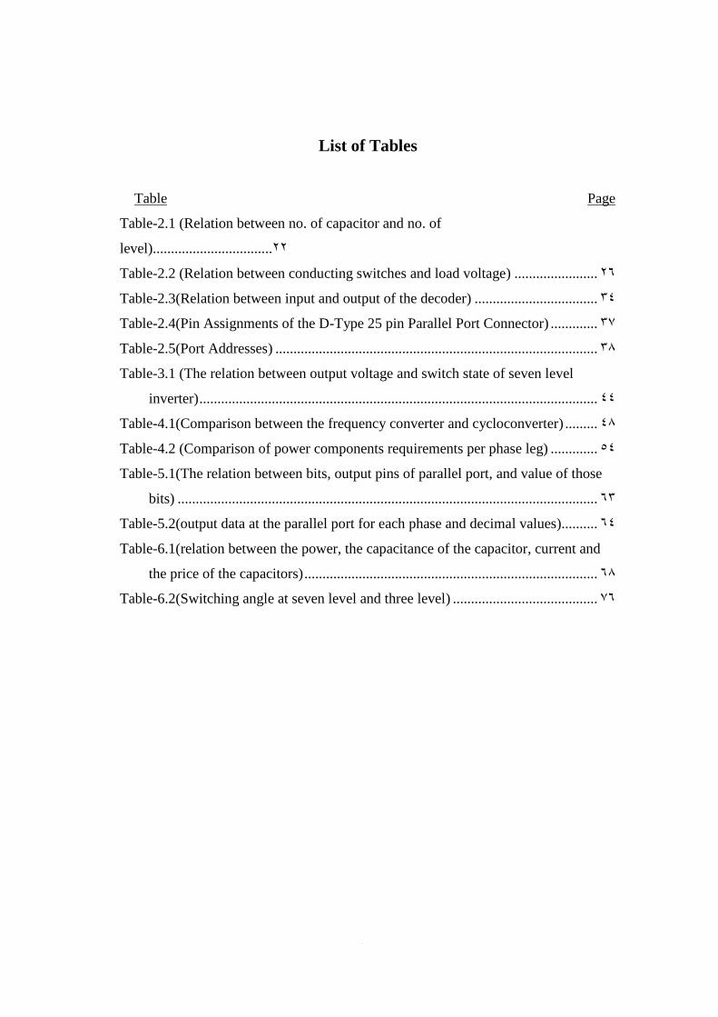
List of Tables
Table Page
Table-2.1 (Relation between no. of capacitor and no. of
level).................................٢٢
Table-2.2 (Relation between conducting switches and load voltage) ....................... ٢٦
Table-2.3(Relation between input and output of the decoder) .................................. ٣٤
Table-2.4(Pin Assignments of the D-Type 25 pin Parallel Port Connector) ............. ٣٧
Table-2.5(Port Addresses) ......................................................................................... ٣٨
Table-3.1 (The relation between output voltage and switch state of seven level
inverter).............................................................................................................. ٤٤
Table-4.1(Comparison between the frequency converter and cycloconverter) ......... ٤٨
Table-4.2 (Comparison of power components requirements per phase leg) ............. ٥٤
Table-5.1(The relation between bits, output pins of parallel port, and value of those
bits) .................................................................................................................... ٦٣
Table-5.2(output data at the parallel port for each phase and decimal values).......... ٦٤
Table-6.1(relation between the power, the capacitance of the capacitor, current and
the price of the capacitors)................................................................................. ٦٨
Table-6.2(Switching angle at seven level and three level) ........................................ ٧٦

XI
List of Figures
Figure Page
Figure-2.1 (3-phase full controlled rectifier) ............................................................. 10
Figure-2.2 (Waveforms of 3-phase full controlled rectifier) ..................................... 11
Figure-2.3 (Relation between Ripple Factor and α) .................................................. 13
Figure-2.4 ({a} curve (w- T) and {b} curve (V - f)) ................................................. 15
Figure-2.5 (Relation between α and f) ....................................................................... 18
Figure-2.6 (a- charging circuit. b- charging voltage and current waveforms).......... 20
Figure-2.7 (a- discharging circuit. b- discharging voltage and current waveforms) 21
Figure-2.8 (3-phase controlled rectifier with DC-Link) ............................................ 22
Figure-2.9 (Voltage Source Inverter(VSI)) ............................................................... 24
Figure-2.10 (Single phase ½ bridge) ......................................................................... 24
Figure-2.11 (Output voltage of single phase ½ bridge) ............................................. 25
Figure-2.12 (Sigle phase full bridge) ......................................................................... 25
Figure-2.13 (Output voltage of single phase full bridge) .......................................... 26
Figure-2.14 (Symbol of E-MOSFET)........................................................................ 28
Figure-2.15 (Typical current curves for various gate-source voltage levels) ............ 29
Figure-2.16 (RC snubber connected across the switching device) ............................ 31
Figure-2.17 (Unsuppressed turn off transient)........................................................... 32
Figure-2.18 (Turn off ringing almost eliminated) ..................................................... 32
Figure-2.19 (Ringing eliminated by snubber)............................................................ 33
Figure-2.20 (Symbol of Optocoupler) ....................................................................... 35
Figure-2.21 (Parallel port) ......................................................................................... 37
Figure-3.1 (Open loop block diagram)…………………...…………………………41
Figure-3.2 (Seven levels stepped output waveform) ................................................. 43
Figure-4.1 (Half wave cycloconverter)...................................................................... 47
Figure-4.2 (Waveform of Half wave cycloconverter) ............................................... 48
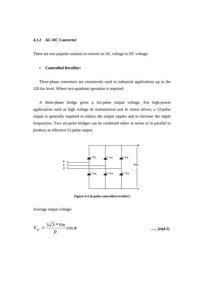
Figure-4.3 (6-pulse controlled rectifier) .................................................................... 49
Figure-4.4 (3-phase uncontrolled rectifier)................................................................ 50
Figure-4.5 (Step-Down DC-Chopper) ....................................................................... 51

XII
Figure-4.6 (Diode-Clamped Multi-level Inverter)..................................................... 52
Figure-4.7 (Flying Capacitor Multi-level Inverter) ................................................... 53
Figure-4.8 (Multi-level Inverter using Cascaded-Inverters with Separated DC
Sources) ............................................................................................................. ٥٣
Figure-4.9 (Frequency Converter With Seven Levels Voltage Source Inverter )…..56
Figure-4.10 (Part one of the Interfacing circuit of seven level diode clamped inverter)
…………………………………………………………………………………58
Figure-4.11 (Isolating (second) part of Interfacing circuit of seven level diode
clamped inverter) ............................................................................................... 59
Figure-5.1 (User Interface) ........................................................................................ 61
Figure-5.2 (Program behavior when an error occures )............................................. 62
Figure-5.3 (Flow Chart)...…...………………………………………………………6٥
Figure-6.2 (Seven levels PWM output waveform).................................................... 70
Figure-6.3 (Waveform synthesis: a- 11-level b- 21-level c- 31-level d- 41-level). 73
Figure-6.4 (Number of levels versus the THD)......................................................... 74
Figure-6.5 (Three-level PWM waveform)................................................................. 77
Figure-6.6 (Seven-level PWM waveform) ................................................................ ٧٧
Figure-6.7 (Phase waveform at different frequency (7-levels))................................. ٧٨
Figure-6.8 (Phase-to-Phase waveform at different frequency (7-levels)) ................. 78
Figure-6.9 (Phase-to-Phase waveform when using the capacitors) ........................... 79
Figure-6.10 (Phase waveform when using the capacitors) ........................................ 79

١
CHAPTER ONE
INTRODUCTION
1.1 Frequency Converter
1.2 Importance of Project
1.3 Good Features
1.4 Project Scope
1.5 Literature Review
1.6 Project Contents

٢
CHAPTER ONE
INTRODUCTION
1.1 Frequency Converter :
Frequency converter allows variable frequency and voltage supply to be obtained
from a fixed voltage and frequency AC supply. This operation is done by converting
an AC fixed voltage into variable dc voltage by using a controlled rectifier such as
six-pulse controlled rectifier (B6C). By using a DC-link (such as capacitors) the dc
output voltage of rectifier is divided into a number of separately dc sources that will
acts as a supply of multilevel voltage source inverter that is operated by pulse width
modulation (PWM) technique . This inverter will provide us with a variable voltage
and frequency.
Multilevel inverter structures have been developed to overcome shortcomings in
solid-state switching device ratings so that they can be applied to high-voltage
electrical systems. The multilevel voltage source inverter is a unique structure allows
them to reach high voltages with low harmonics without the use of transformers.
This makes these unique power electronics topologies suitable for flexible ac
transmission systems (FACTS) and custom power applications. The use of a
multilevel converter to control the frequency, output voltage (including phase angle),
and real and reactive power flow at a dc/ac interface provides significant
opportunities in the control of distributed power systems.
The output voltage waveforms of ideal inverters should be sinusoidal. Whereas,
the waveforms of practical inverters are non- sinusoidal and contain harmonics.

٣
1.2 Importance of Project :
It is well-known fact that the speed of an AC motor depends primarily on the
pole number of the motor and the frequency of the voltage supplied. The amplitude
of the voltage supplied and the load on the motor shaft also influence the motor
speed, however not to the same degree.
Consequently, changing the frequency of the supply voltage is an ideal method
for AC motor speed control. In order to ensure a correct motor magnetization and
constant breakdown torque, it is also necessary to change the amplitude of the
voltage in order to obtain a constant ratio between the voltage and frequency (V/f =
constant).
Multilevel pulse width modulation (PWM) inverters have been developed to over
come shortcomings in solid state switching device ratings so that large motors can be
controlled by high power adjustable frequency drives. PWM technique in multilevel
inverters reduces the number of level needed to reduce the required harmonics from
the output voltage of inverters. The most popular structure proposed as a
transformerless voltage source inverter is the diode clamped converter.
This project has the ability of working as an open loop system. Also in this
project we will use a personal computer to control all parts in the system such as the
control of the multilevel diode clamped inverter and this is a modern controlling
method.

٤
1.3 Good Features:
There are four main good features in this project:
The idea of building a six pulse controlled rectifier (B6C) which provide us a
variable dc voltage (instead of separate dc sources) which is used as an input
of multi-level diode clamped inverter to control of its output voltage.
Building DC–link that is followed the rectifier to divide the output dc voltage
into levels.
The idea of building the inverter with multilevel technique based on pulse
width modulation (PWM) is to reduce harmonics, control the output voltage,
and overcome shortcomings in solid state switching device ratings.
Using the personal computer as a controller for the switching angles of
multilevel (PWM) by using a suitable interface circuits.
1.4 Project Scope :
The project is concerned with the following critical points:
Open loop speed control of AC motors.
Controlling of the input dc voltage of inverter by using a three phase full
controlled rectifier (B6C).
Number of levels which used to reduce the harmonics as far as possible.
How the number of levels will affect on the characteristics of inverters.
How PWM technique will reduce the harmonics at the same number of
levels.
The methods that are used to analysis the output complex waveforms with
PWM.
The way to select switching angles at which the output voltage not contain
harmonics which closer to fundamental harmonic is using numerical analysis

٥
for solving large non-linear equations by using Fourier analysis and Newton
Raphson method .
On the other hand the project will study how it can be interfaced the inverter
and rectifier with personal computer, and the electronic circuits for this aim,
also the software to generate the pulses.
1.5 Literature Review:
Many of electrical scientist make studies about the different types of multilevel
inverter such as diode clamped multilevel inverter, flying capacitor multilevel
inverter and the cascade multilevel inverter.
One of these studies which talk about the multilevel modulation (PWM) inverter
which have been developed to overcome shortcomings in solid state switching devise
so that large motors can be controlled by high-power adjustable frequency drives.
The most popular structure proposed as a transformerless voltage source inverter is
the diode clamped converter based on the neutral point converter proposed by Nabac.
[5]
This kind of multilevel inverter is one of the unique structure allows them to each
high voltage with low harmonics without the use of transformers. The general
function of the multilevel inverter is to synthesize a desired voltage from several
levels of de voltage. For this reason, multilevel inverter can easily provide the high
power required of a large electric drive.
As the number of levels increases, the synthesized output waveform has more
steps, which produces a staircase wave added to the waveform, the harmonic
distortion of the output wave decreases approaching zero as the number of levels

٦
increases. The structure of the multilevel inverter is such that no voltage sharing
problems are encountered by the series-connected devices. [7]
Also, the study that prepared by L. Tolbert and F. Peng explain that the
multilevel converters have many advantages such as: 1) they are more suitable for
medium and large VA rated motor drives. 2) Their efficiency is much higher because
of the minimum switching frequency. 3) Power factor is close to unity for multilevel
inverters used as a rectifier to convert generated ac to dc. 4) No voltage sharing
problems exist for series connected devices unlike traditional inverters. [6]
1.6 Project Contents
Chapter one explains what is the frequency converter which is this project; also it
contains the importance of project and project scope. On the other hand, it contains
the previous studies about the project.
In chapter two, there is a full information about the three phase full controlled
rectifier, the DC-Link that is connected between the three phase controlled rectifier
and the seven level diode clamped inverter. Also, it contains an analysis of each part
of project, such as it contains analysis about the relation between the triggering angle
and frequency. On the other hand it contains an information about the devices in the
project.
Chapter three explains the objective of the project. Also it contains the general
open loop block diagram. also, this chapter explains how system works.
In chapter four, there are different design options and comparison between them;
also it contains the Hardware design of the project.

٧
Chapter five contains an information about the visual basic program and it
contains the flow chart of the project program. Also, it describes the method of
programming the parallel port.
In chapter six there is an analysis of DC-Link, seven level waveform with PWM
and results analysis. Chapter seven contains the conclusion and future work.

٨
CHAPTER TWO
THEORETICAL BACKGROUND
2.1 Three–Phase Full Controlled Rectifier
2.1.1 Introduction
2.1.2 Triggering Process
2.1.3 Why V/f = Constant?
2.1.4 The Relation between α and f
2.2 Harmonics in Electrical Systems
2.3 DC -Link
2.4 Multilevel Inverter
2.5 The Voltage Source Inverter (VSI)
2.6 Multilevel Voltage Source Inverter
2.7 The Newton-Raphson Method
2.8 Hardware Devices
2.8.1 Power MOSFETs (N-channel Enhancement)
2.8.1.1 Switching Transient Experiments
2.8.1.2 Transient Suppression Results
2.8.2 Heat Sink
2.8.3 Digital Components
2.8.4 PC Parallel Port

٩
CHAPTER TWO
THEORETICAL BACKGROUND
2.1 Three–Phase Full Controlled Rectifier:
2.1.1 Introduction
Three-phase full controlled rectifier is extensively used in industrial applications
up to the 120 kw level, where two-quadrant operation is required. Figure (2.1) shows
a three phase full-controlled rectifier circuit (B6C). The thyristors are fired at an
interval of /3. The frequency of output ripple voltage is 6fs (fs: source frequency)
and the filtering requirement is less than that of three-phase semi- and half-wave
converters. At wt = /6 + α , thyristor T6 is already conducting and thyristor T1 is
turned on. During interval ( /6 + α) ≤ ( /2 + α), thyristor T1 and T6 conduct and
the line -to-line voltage, Vab= (Van –Vbn) appears across the load.
At wt = /2 + α, thyristor T2 is fired and thyristor T6 is reversed biased
immediately. T6 is turned off due to natural commutation. During interval ( /2 + α)
≤ wt ≤ (5 /6 + α), thyristor T1 and T2 conduct and the line to line voltage, Vab
appears across the load. If the thyristors are numbered as shown in Figure (2.1), the
firing sequence is 12, 23, 34, 45, 56, and 61. Figure (2.2) shows the waveforms for
input and output voltage, input current and currents though thyristors, for high
inductive load.

١٠
LoadVdc
T1 T3
T6 T2T4
T5
a
cb
Figure-2.1 (3-phase full controlled rectifier)
If the line-to-neutral voltage is defined as:
)3/2sin(
)3/2sin(
sin
tVV
tVV
tVV
mcn
mbn
man
The corresponding line–to–line voltages are:
)2/sin(*3
)2/sin(*3
)6/sin(*3
tVVVV
tVVVV
tVVVV
mancnca
mcnbnbc
mbnanab
….. (eq2.1)
….. (eq2.2)

١١
Figure-2.2 (Waveforms of 3-phase full controlled rectifier)
The average output voltage (Vdc) is found from:
cos*33 m
dcV
V ….. (eq2.3)
VVV
VV
LLs
sm
22033803
*2
….. (eq2.4)

١٢
Where:
Vs : Phase Voltage
VL-L : Line to Line Voltage
Vm : Peak Voltage
The maximum average output voltage at = 0 is:
VV
Vm
dc 86.514)220*2(*33*33
max
And the normalized average output voltage is:
cosmax dcdcn VVV ….. (eq2.5)
The rms value of the output voltage is found from:
11.5154
335.0*220*2*3
2cos4
335.0*3
max
rms
mrms
V
VV
The Form Factor which is a measure of the shape of output voltage is:
00049.186.51411.515maxmaxmax
dcrms
dcrms
VVFF
VVFF
….. (eq2.6)
….. (eq2.7)

١٣
The Ripple Factor (R.F.) which is a measure of the ripple content is defined as:
%1.3%100*031.0100049.1
11
2
22
FFVVVVRF dcrmsdcac
The following figure(2.3) shows the relationship between ripple factor (R.F.) and
triggering angle (α).
Figure-2.3(Relation between Ripple Factor and α)
2.1.2 Triggering Process:
In this project we will use the pulse generator with control circuits to trigger the
six thyristors, (the sequence of triggering thyristors is illustrated previously and as
shown in figure (2.2))
….. (eq2.8)

١٤
The firing angles are determined according to the required speed of induction
motor which depends on the voltage and frequency. In order to change the voltage,
the firing angles must be changed in certain values convenient for changing of speed.
The changing of voltage must be followed with changing in frequency in order to
keep the ratio between the voltage and frequency constant (V/f = constant). This ratio
can be controlled by using the PC.
In order to avoid the short circuit the triggering process must be occurred in the
firing sequence such as T1 T2 , T2 T3 , T3 T4 , T4 T5 , T5 T6 , T6 T1 . So we must not
trigger the thyristors T1 T4 , T3 T6 or T5 T2 at the same time.
2.1.3 Why V/f = Constant?
The motor speed can be controlled by varying supply frequency. Voltage induced
in stator is proportional to the product of supply frequency and air-gap flux. If stator
drop is neglected, terminal voltage can be considered proportional to the product of
frequency and flux. In order to avoid saturation and to minimize losses, motor is
operated at rated air-gap flux by varying terminal voltage with frequency so as
maintain (V/f) ratio constant at the rated value.
Equation (eq2.10) shows that with a constant (V/f) ratio, motor develops a
constant maximum torque, except at low speeds (or frequencies). Motor therefore
operates in constant torque mode. According to equation (eq2.9), maximum torque
will have lower value for low frequencies (or speeds) due to stator resistance drop.
When it is required that the same maximum torque is retained at low speeds also,
(V/f) ratio is increased at low frequencies.
For controlling of speed of induction motor under the rated value, the frequency
must be changed with the voltage. When either V saturates or reaches rated value at

١٥
base speed, it cannot be increased with frequency in order to maintain a constant
(V/f) ratio. Therefore, above rated speed, frequency is changed with V maintained
constant (Figure-2.4), giving a constant power operation and reduction in the
maximum torque with increase in frequency.
Figure-2.4 ({a} curve (w- T) and {b} curve (V - f))
222
2
2
22
2
max
4
2
3
rsss
rss
LLTfRfR
V
f
K
xxRsRws
VT
When frequency is not low 0 fRs
rs LLT
fVKT
2
2
max
….. (eq2.9)
….. (eq2.10)

١٦
.: constfVfnfFor
VnVfnf
2.1.4 The Relation between α and f:
The following analysis explains the relation between the triggering angle (α) and
the frequency (f).
cos6.514cos13.31133
13.3113
380232
cos33
dc
LLm
mdc
V
VVV
VV
cos25.315
22
cos6.5143
22
3
2
633
2
33
23
'
dcdc
cmLL
VV
VVV
out….. (eq2.11)

١٧
Bf
Bff
Vout
LL
cos25.315
cos25.315
cos50305.650
25.315max
f
f
VB
n
LL
n
Where:
Vdc : Output Voltage of Rectifier.
VL-L : Input Line to Line Voltage.
VL-Lout : Output Line to Line Voltage of Inverter.
Vc : Voltage at Capacitor.
Vm : Peak Input Voltage.
Vm' : Peak Output Voltage.
f : Frequency.
α : Triggering Angle.
B : Ratio Between VL-Lout and f.
The following figure (2.5) illustrates the relationship between the frequency (f)
and the triggering angle (α) as given in the equation (eq2.12) with different values of
B.
….. (eq2.12)

١٨
Figure-2.5 (Relation between α and f)
2.2 Harmonics in Electrical Systems:
One of the biggest problems in power quality aspects is the harmonic contents in
electrical systems. Generally, harmonics may be divided into two types: 1) voltage
harmonics, and 2) current harmonics. Current harmonics is usually generated by
harmonics contained in voltage supply and depends on the type of load such as
resistive load, capacitive load and inductive load. Both harmonics can be generated
by either the source or the load side. Harmonics generated by load are caused by
nonlinear operation of devices, including power converters, arc-furnaces, gas
discharge lighting devices, etc. Load harmonics can cause the overheating of the
magnetic cores of transformer and motors. On the other hand, source harmonics are
mainly generated by power supply with non-sinusoidal voltage waveform. Voltage
and current source harmonics imply power losses, Electromagnetic Interference
(EMI) and pulsating torque in AC motor drives. Any periodic waveform can be
shown to be the superposition of a fundamental and a set of harmonic components.

١٩
By applying Fourier transformation, these components can be extracted. The
frequency of each harmonic component is an integral multiple of its fundamental.
There are several methods to indicate of the quantity of harmonics contents.
The most widely used to measure the total harmonics distortion (THD), which is
defined in terms of the amplitudes of the harmonics, Hn, at frequency nw0, where w0
is frequency of the fundamental component whose amplitude of H1 and n is integer.
The THD is mathematically given by
1
2
2
H
HTHD n n
….. (eq2.13)
2.3 DC -Link:
In general, the DC-link that is used in multilevel diode clamped inverter is a
number of capacitors that is connected in series to divide the DC input voltage of
inverter into a set of voltage levels. At the beginning of charging of capacitor, it acts
as a short circuit , but after a time equals to 5t ( where t = R*C ) , the capacitor acts
as a dc battery . The capacitor will be charged with a voltage nearly equals to the
source voltage with a time equals to 5t, whereas the current will decrease. The charge
(Q) at the capacitor is equal to C*V. The following equations and figure(2.6)
represent the charging condition.
)1( )/( RCteEVc ….. (eq2.14)
RCteR
VcIc ….. (eq2.15)

٢٠
Where:
E : Source Voltage.
Ic : Charging Current.
R : Charging Resistance.
C : Capacitance.
t : Charging Time.
Vc: Capacitor Voltage
Figure-2.6(a- charging circuit. b- charging voltage and current waveforms)
In discharge condition the capacitor will loss it’s charge and the voltage on it will
drop to zero with a time equals to 5t, also the current direction changes and its value
will decrease . The following equations and figure(2.7) represent this condition.

٢١
RCteEVc / ….. (eq2.16)
RCteR
EIc / ….. (eq2.17)
Figure-2.7(a- discharging circuit. b- discharging voltage and current waveforms)
The Operation of DC – Link:
In order to build a three phase m-levels diode clamped inverter we need (m-1)
capacitors. Each capacitor has voltage equal to Vdc (output of rectifier) divided by
(m-1).
In this project we will build a three phase 7-level diode clamped inverter, so we
need six capacitors as a separate dc voltage sources ( figure-2.8).

٢٢
Vdc
T1 T3
T6 T2T4
T5
a
cb
3-Phase Controlled Rectifier DC-Link
0.22F1
+ C1
+ C2
+ C3
+ C4
+ C5
+ C6
Figure-2.8 (3-phase controlled rectifier with DC-Link)
To construct a level one (zero voltage) no capacitor must be used. For level two
(85.8 maximum voltage) one capacitor must be used, and for level three (171.6
maximum voltage) two capacitor must be used, and so on. The following table (2.1)
will explain this operation:
Table-2.1 (Relation between no. of capacitor and no. of level)
Number of
capacitors
Number of
level
Maximum output
voltage(Volt)
0 1 0
1 2 85.8
2 3 171.6
3 4 257.4
4 5 343.2
5 6 429
6 7 514.8

٢٣
2.4 Multilevel Inverter
A multilevel converter is a power electronic system that synthesizes AC voltage
of desired magnitude and frequency. The output voltage could be fixed or variable at
a fixed or variable frequency. The variable output voltage can be obtained by varying
the input DC voltage that is obtained from a number of capacitors (DC-Link) that are
changed by the output DC voltage of the six-pulse three phase controlled rectifier
(B6C).
The output voltage waveforms of ideal inverters should be sinusoidal. Whereas
the waveforms of practical inverters are non-sinusoidal and contain certain
harmonics.
Use of multilevel inverters is becoming popular in the recent years for high
power applications.Various topologies and modulation strategies have been reported
for utility and drive applications in the recent literature.
Multilevel pulse width modulation (PWM) inverters have been developed to
overcome shortcomings in solid state switching device ratings so that large motors
can be controlled by high-power adjustable frequency drives, and PWM technique in
multilevel inverters reduce the number of level needed to reduce the required
harmonics from the output voltage of inverters. The most popular structure proposed
as a transformerless voltage source inverter is the diode clamped converter.
Investigators have proposed carrier-based multilevel sine-triangle PWM schemes for
control of a multilevel diode clamped inverter used as a motor drive or static variable
compensator.
A PWM method is used to control a multilevel diode clamped converter for
selective harmonic elimination by adjusting the width of pulse to the band of width
required to cancel n-harmonic. While the multilevel PWM techniques developed thus

٢٤
far have been extensions of two-level PWM methods, the multiple levels in a diode-
clamped inverter offer extra degrees of freedom and greater possibilities in terms of
device.
2.5 The Voltage Source Inverter (VSI):
Figure-2.9 (Voltage Source Inverter(VSI))
The simplest form is the single phase ½ bridge. The devices might be MOSFETs
SCRs BJTs or GTOs.
Figure-2.10 (Single phase ½ bridge)
S1 is turned on to give the +ve half cycle, and S2 is turned on to give the –ve half
cycle. Clearly care must be taken to avoid both circuits being turned on at the same
time.

٢٥
D1 and D2 carry current when it is –ve in the first half and +ve in the second
half, such as might be the result of a lagging load. D1 and D2 are called feedback
diodes. For the operation of this converter, the midpoint, V/2 is required, although
this is not the case for most inverters.
Figure-2.11 (Output voltage of single phase ½ bridge)
The Full Bridge Converter:
Figure-2.12 (Sigle phase full bridge)
Again the devices can be any of the power switches already encountered and the
diodes are termed feedback diodes.

٢٦
During the first half of the output the voltage across the load, vo is +ve, this is
achieved by firing S1 and S4 simultaneously. If the load is inductive then the current
Io lags the voltage vo. There must be a path for the –ve current. This path is achieved
by inserting D1 and D2 into the circuit. Firing S3 and S2 creates the –ve half cycle.
The following table (2.2) illustrates this operation.
Table-2.2 (Relation between conducting switches and load voltage)
Conducting switches Load voltage
S1 , S4 + Vs
S2 , S3 - Vs
S1 , S2 or S3 , S4 0
Figure-2.13 (Output voltage of single phase full bridge)
2.6 Multilevel Voltage Source Inverter:
The multilevel voltage source inverter is recently applied in many industrial
applications such as ac power supplies, static VAR compensators, drive systems,

٢٧
etc.. One of the significant advantages of multilevel configuration is the harmonic
reduction in the output waveform without increasing switching frequency or
decreasing the inverter power output. The output voltage waveform of a multilevel
inverter is composed of the number of levels of voltages, typically obtained from
capacitor voltage sources. The so-called multilevel starts from three levels. As the
number of levels reach infinity, the output THD approaches zero. The number of the
achievable voltage levels is limited by voltage unbalance problems, voltage clamping
requirement, circuit layout, and packaging constraints.
So three capacitor voltage synthesis-based multilevel inverters are introduced, i.e.
1) Diode-Clamped Multilevel Inverter.
2) Flying-Capacitor Multilevel Inverter.
3) Cascaded-Inverters with Separated DC Sources.
2.7 The Newton-Raphson Method:
The Newton-Raphson method (or simply Newton’s) method is one of the most
powerful and well-known numerical methods for computing the root of an equation.
It is a successive-approximation procedure, which is suitable for implementation in a
computer program. Generally, the system of nonlinear equation in s variables can be
represented as:
f1 ( 1 , 2 , 3……, s) = k1
f2 ( 1 , 2 , 3……, s) = k2
.
.
.
fs ( 1 , 2 , 3……, s) = ks

٢٨
Then,
F ( ) = k
And:
F = [ f1 , f2 ,…………., fs ]
F/ = [ f1 , f2 ,…………., fs-1 ]
= [ 1 , 2 , ……, s]
/ = [ 1 , 2 , ……, s-1]
k = [ k1 , k2 , ………….,ks ]
k/ = [k1 , k2 , ………….,ks-1]
Where: F , F/ , , / , k , k/ are matrices.
Then we can find the itrations ( ) by apply the Newton’s method form as in
the following equation:
[ ] = [ /] - INV[dF//d /] [F/-k/] ….. (eq2.18)
2.8 Hardware Devices
2.8.1 Power MOSFETs (N-channel Enhancement):
The MOSFET is a three terminal device consisting of a source, drain and gate.
The symbol is:
Figure-2.14(Symbol of E-MOSFET)

٢٩
The gate-source voltage level controls the current. The minimum VGS that
creates the n-type inversion layer is called the threshold voltage, symbolized VGS (th)
.When VGS is less than VGS(th) , the drain current is zero. When VGS is greater than
VGS (th) ,an n-type inversion layer connects the source to the drain and the drain
current can flow .Typical values of VGS(th) for small-signal devices are from 1 to 3
volt. The diagram below shows typical current curves for various gate-source voltage
levels.
Figure-2.15(Typical current curves for various gate-source voltage levels)
The lowest curve is the VGS(th) curve . When VGS is less than VGS(th) , the drain
current is approximately zero . When VGS is greater than VGS(th) , the device turns on
and the drain current is controlled by the gate voltage . The almost vertical part of the
figure is the ohmic region, and the almost horizontal parts are the active region.
When biased on in the ohmic region, the E-MOSFET is equivalent to a resistor.
When biased in the active region, it is equivalent to a current source. Although the E-
MOSFET can operate in the active region, the main use is in the ohmic region.

٣٠
For the purposes of simply current switching, the MOSFET should be operated
within the constant resistance region. This means that for maximum current capacity
the gate-source voltage should be pulsed at the correct value. If you take a look at a
typical power MOSFET data sheet you'll find a set of current curves like those
above. At higher gate-source and drain-source voltages the current has a more
complicated characteristic.
Some MOSFETs are protected by a built-in zener diode in parallel with the gate
and the source. The zener voltage is less than the VGS(max.) rating . Therefore, the
zener diode breaks down before any damage to the thin insulating layer occurs . The
disadvantage of these internal zener diodes is that they reduce the MOSFET’s high
input resistance. The trade-off is worth it in some applications because expensive
MOSFETs are easily destroyed without zener diodes protection.
2.8.1.1 Switching Transient Experiments
This section look at the type of overshoot and ringing, which occurs after
a switching event. There are several possible methods, which can be
employed to remove the overshoot and ringing. The first experiment uses a
small snubber to remove the ringing portion of the transient. Figure (2.16)
shows how the snubber is connected to the switching circuit.

٣١
Figure-2.16(RC snubber connected across the switching device)
The snubber works simply by providing a low impedance path to ground
for high frequency voltages. The only parameter, which is measured in this
experiment, is the D-S voltage of the MOSFET.
Two different snubbers were used - one composed of a 100Ω resistor
and a 0.2μF capacitor, the other formed from a 25Ω resistor and a 0.3μF
capacitor. The resistors were plain carbon types and the capacitors were
polycarbonate.
2.8.1.2 Transient Suppression Results
This section shows that a small RC snubber connected across the
MOSFET switching device can eliminate the turn off ringing. The
oscilloscope trace for an unsuppressed clamped coil B is shown in
figure(2.17).

٣٢
Figure-2.17(Unsuppressed turn off transient)
Clearly the ringing is very pronounced and could interfere with circuitry.
The effect of the addition of a RC snubber can be seen in figure(2.18).
Figure-2.18(Turn off ringing almost eliminated)
Reducing the size of the resistor and increasing the value of the capacitor
completely removes the ringing as shown in figure(2.19).

٣٣
Figure-2.19(Ringing eliminated by snubber)
Although this small snubber can remove the ringing we are still left with
the large overshoot. In fact the snubber appears to have no significant effect
on the shape of the overshoot. In order to reduce the overshoot we would
require a much larger snubber and this could impact the switching time for
the MOSFET. So we select a snubber of 1μF and resistance 33 Ω.
This overshoot is very short and is well within the avalanche capability
of the MOSFET module; however, the waveform still contains sharp voltage
transitions, which could be capacitively coupled into sensitive circuitry.
2.8.2 Heat Sink
A heat sink is a device that is attached to semiconductor devices to keep them
from overheating by absorbing their heat and dissipating it into the air. Since all
semiconductor devices have some electrical resistance, just like resistors and coils,
etc. This means that when power diodes, power transistors and power MOSFETs are
switching or otherwise controlling reasonable currents, they dissipate power as heat
energy. If the device is not to be damaged by this, the heat must be removed from
٣٤
inside the device (usually the collector-base junction for a bipolar transistor, or the
drain-source channel in a MOSFET) at a fast enough rate to prevent excessive
temperature rise. The most common way to do this is by using a heat sink.
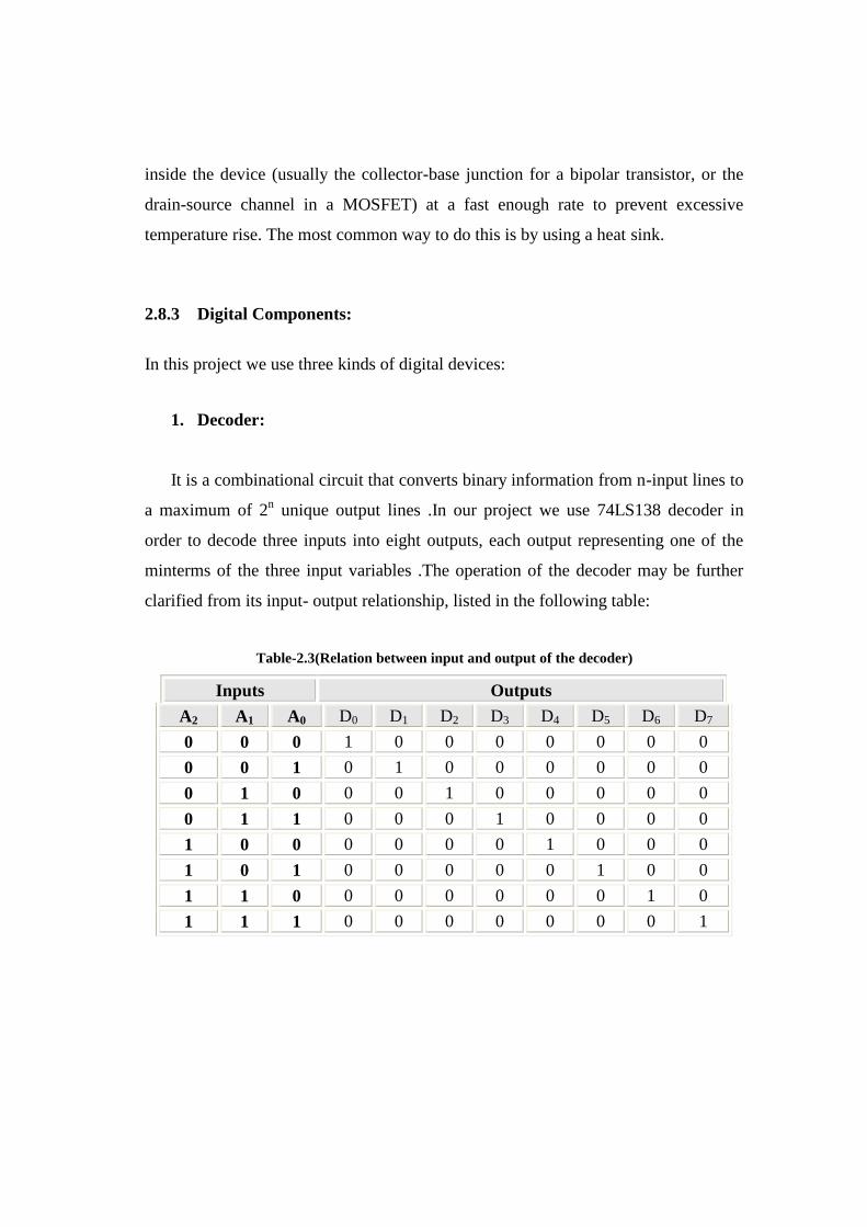
2.8.3 Digital Components:
In this project we use three kinds of digital devices:
1. Decoder:
It is a combinational circuit that converts binary information from n-input lines to
a maximum of 2n unique output lines .In our project we use 74LS138 decoder in
order to decode three inputs into eight outputs, each output representing one of the
minterms of the three input variables .The operation of the decoder may be further
clarified from its input- output relationship, listed in the following table:
Table-2.3(Relation between input and output of the decoder)
OutputsInputs
D7D6D5D4D3D2D1D0A0A1A2
0000000100000000010100
00000100010
0000100011000010000001
00100000101
0100000001110000000111

٣٥
2. Inverter:
The inverter circuit inverts the logic sense of a binary number. If the input of
inverter is one, the output will be zero, also when the input is zero the output will be
one.
3. Optocoupler :
The optocoupler contains LED and phototransistor (Figure-2.20). The source
voltage at the input of optocoupler provides the LED with a suitable current that is
converted into photo signal. This photo signal will trigger the phototransistor in order
to pass the current from the collector to emitter. Any changes in source voltage
produce changes in the LED current, which changes the current through the
phototransistor. In turn, this produces a changing voltage across the collector –
emitter terminals. Therefore, a signal voltage is coupled from the input circuit to the
output circuit.
The big advantage of an optocoupler is the electrical isolation between the input
and output circuits. Stated another way, the common for the input circuit is different
from the common of the output circuit. Because of this, no conductive path exists
between the two circuits. This means that you can ground one of the circuits and
float the other. For instance, the input circuit can be grounded to the chassis of the
equipment, while the common of the output side is ungrounded.
OP4N25OP4N25
Figure-2.20(Symbol of Optocoupler)

٣٦
2.8.4 PC Parallel Port
The Parallel Port (Figure-2.21) is the most commonly used port for
interfacing home made projects. This port will allow the input of up to 17
bits or the output of 12 bits at any one given time, thus requiring minimal
external circuitry to implement many simpler tasks. The port is composed of
4 control lines, 5 status lines and 8 data lines. It's found commonly on the
back of your PC as a D-Type 25 Pin female connector. There may also be a
D-Type 25 pin male connector. This will be a serial RS-232 port and thus, is
a totally incompatible port.
Below is a table(2.4) of the "Pin In/Outs" of the D-Type 25 Pin
connector and the Centronics 34 Pin connector. The D-Type 25 pin
connector is the most common connector found on the Parallel Port of the
computer, while the Centronics Connector is commonly found on printers.
The IEEE 1284 standard however specifies 3 different connectors for use
with the Parallel Port. The first one, 1284 Type A is the D-Type 25
connector found on the back of most computers. The 2nd is the 1284 Type
B, which are the 36 pins Centronics Connector found on most printers
IEEE 1284 Type C however, is a 36 conductor connector like the
Centronics, but smaller. This connector is claimed to have a better clip latch,
better electrical properties and is easier to assemble. It also contains two
more pins for signals, which can be used to see whether the other device
connected, has power. 1284 Type C connectors are recommended for new
designs, so we can look forward on seeing these new connectors in the near
future.

٣٧
Figure-2.21(Parallel port)
Table-2.4(Pin Assignments of the D-Type 25 pin Parallel Port Connector)
Pin No(D-Type
25)
Pin No(Centronics) SPP Signal
DirectionIn/out Register
HardwareInverted
1 1 nStrobe In/Out Control Yes
2 2 Data 0 In/Out Data
3 3 Data 1 In/Out Data
4 4 Data 2 In/Out Data
5 5 Data 3 In/Out Data
6 6 Data 4 In/Out Data
7 7 Data 5 In/Out Data
8 8 Data 6 In/Out Data
9 9 Data 7 In/Out Data
10 10 nAck In Status
11 11 Busy In Status Yes
12 12Paper-Out /Paper-End
In Status
13 13 Select In Status
14 14nAuto-
LinefeedIn/Out Control Yes
15 32 nError / nFault In Status
16 31 nInitialize In/Out Control
17 36nSelect-Printer
/ nSelect-InIn/Out Control Yes
18 - 25 19-30 Ground Gnd

٣٨
The above table(2.4) uses "n" in front of the signal name to denote that
the signal is active low. e.g. nError. If the printer has occurred an error then
this line is low. This line normally is high, should the printer be functioning
correctly. The "Hardware Inverted" means the signal is inverted by the
Parallel card's hardware. Such an example is the Busy line. If +5v (Logic 1)
was applied to this pin and the status register read, it would return back a 0
in Bit 7 of the Status Register.
Port Addresses:
The Parallel Port has three commonly used base addresses. These are
listed in table(2.5), below. The 3BCh base address was originally introduced
used for Parallel Ports on early Video Cards. This address then disappeared
for a while, when Parallel Ports were later removed from Video Cards. They
has now reappeared as an option for Parallel Ports integrated onto
motherboards, upon which there configuration can be changed using BIOS.
LPT1 is normally assigned base address 378h, while LPT2 is assigned
278h. However this may not always is the case as explained later. 378h &
278h have always been commonly used for Parallel Ports. The lower case h
denotes that it is in hexadecimal. These addresses may change from machine
to machine.
Table-2.5(Port Addresses)
Address Notes:
3BCh - 3BFh Used for Parallel Ports which wereincorporated on to Video Cards
378h - 37Fh Usual Address For LPT 1
278h - 27Fh Usual Address For LPT 2

٣٩
CHAPTER THREE
DESIGN CONCEPTS
3.1 Objectives
3.2 General Block Diagram
3.3 How System Works

٤٠
CHAPTER THREE
DESIGN CONCEPTS
3.1 Objectives:
It is well known that the speed of an Induction motor depends primarily on the
pole number of the motor and the frequency of the voltage supply.
The amplitude of the voltage supply and the load on the motor shaft also
influence the motor speed, however not to the same degree. Consequently, changing
the frequency of the supply voltage is an ideal method for induction motor speed
control. In order to ensure a correct motor magnetization and a constant breakdown
torque, it is also necessary to change the voltage supply in order to obtain a constant
ratio between the voltage and frequency (V/f = constant) and this is the main
objective of the project.
Another objective of our project is building a multilevel inverter with low
harmonics and suitable power for induction motor.
This project has the ability of working as an open loop system. Also in this
project we will use a personal computer to control of all parts in the system such as
control of the multi-level diode clamped inverter and this is a modern controlling
method.
٤١
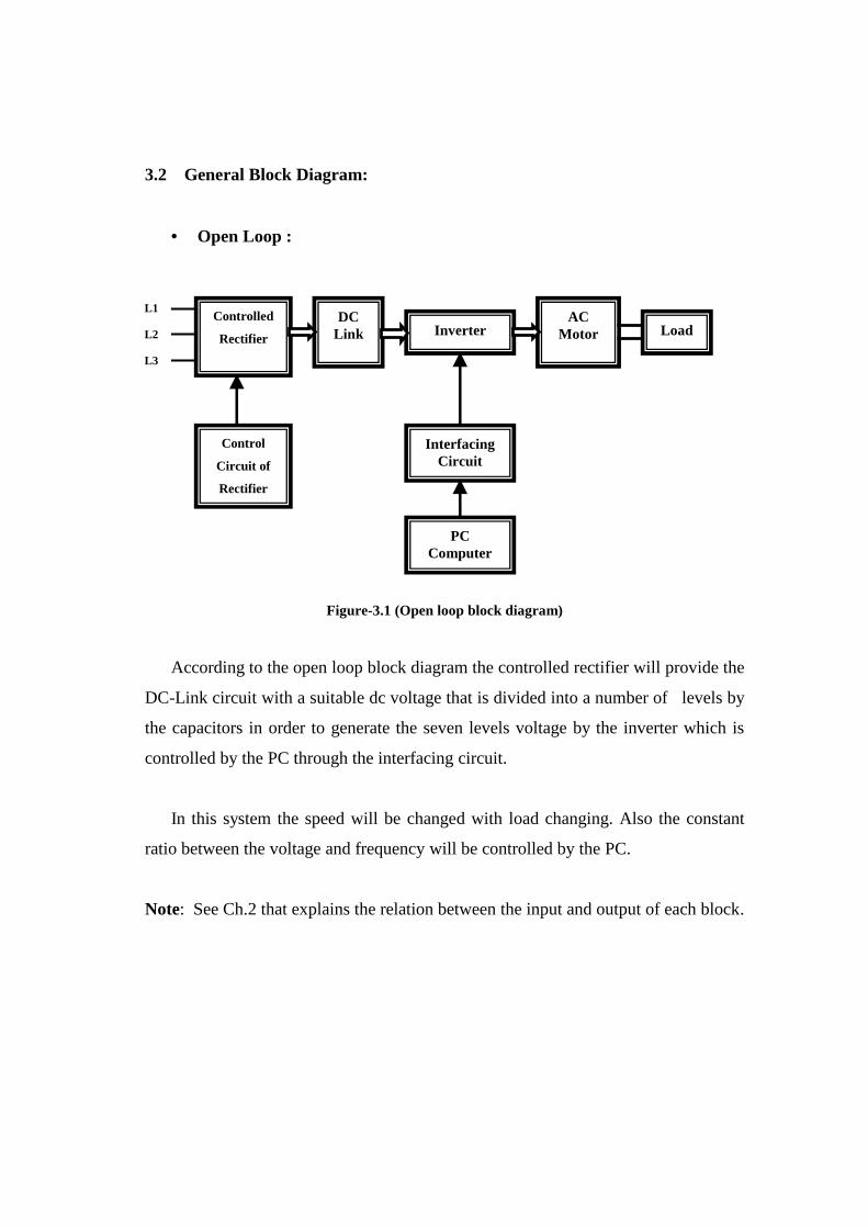
3.2 General Block Diagram:
Open Loop :
Figure-3.1 (Open loop block diagram)
According to the open loop block diagram the controlled rectifier will provide the
DC-Link circuit with a suitable dc voltage that is divided into a number of levels by
the capacitors in order to generate the seven levels voltage by the inverter which is
controlled by the PC through the interfacing circuit.
In this system the speed will be changed with load changing. Also the constant
ratio between the voltage and frequency will be controlled by the PC.
Note: See Ch.2 that explains the relation between the input and output of each block.
Controlled
Rectifier
DCLink Inverter
ACMotor Load
InterfacingCircuit
PCComputer
L1
L2
L3
Control
Circuit of
Rectifier

٤٢
3.3 How System Works:
The main objective of this project is to obtain variable voltage and frequency
from a constant AC-Source (3-phase). In order to accomplish these objectives we
will build:
1- Three-phase six pulse full controlled Rectifier:
It is used to convert a three-phase ac voltage into variable output dc voltage
(figure-2.1). This voltage is controlled by a firing angle of the six thyristors which is
trigged by using the external control circuit that will provide a signal for each two
thyristors. The external control circuit contains the potentiometer which used to
change the triggering voltage that will change the triggering angle, and it contains the
point limiter that limits the firing angle, also it contains the pulse generator which is
used to synchronize the triggering process.
2- DC – Link:
The dc output voltage of rectifier is divided into a number of voltage levels by
using a six capacitors as a dc link (figure-2.5) that connected in series at the output of
the controlled rectifier. Each capacitor will be charged with a maximum voltage
equal to (Vdc/6). The charging voltage at each capacitor will be changed according
to the changing in the output dc voltage of rectifier.
3- Seven – Level Diode Clamped Inverter:
The DC-Link which is connected to the input of seven-level diode clamped
inverter will provide it with the suitable voltage for each level. Figure (3.2) illustrates
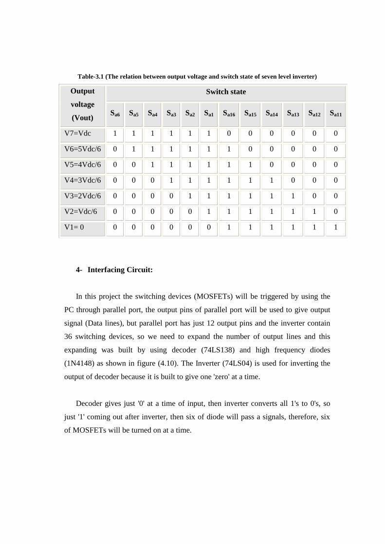
the seven level stepped output voltage. To generate a level one for phase A C1 will

٤٣
provide a dc voltage equal to "Vdc/6" and the switches (Sa6,Sall,..Sa15) must be on, and
the switches (Sa1-Sa5,Sa16) must be off. For level- tow, C1 and C2 must be used to
provide a dc voltage equal to "2 Vdc/6" and the switches (Sa5….Sa14) must be on, also
the switches (Sa1-Sa4,Sa15,Sa16) must be off . This operation is applied to generate the
other levels according to the table (3.1) and figure (4.9). For phase B and C the same
steps is used but with a suitable delay (120o for phase B and -120o for phase C) and
this will be done through the software program.
To explain how the staircase voltage is synthesized, point O is considered as the
output phase voltage reference point. Using the seven-level inverter shown in figure
(4.9), there are six switch combinations to generate seven-level voltages across A
and O.
Table (3.1) explains the phase voltage level and their corresponding switch states.
From this table, state (1) represents that the switch is on, and state (0) represents the
switch is off. In each phase leg, a set of six adjacent switches is on at any given time.
There exist six complimentary switch pairs in each phase, i.e., Sa1-Sa11, Sa2-Sa12, …,
and Sa6-Sa6 .
Figure-3.2 (Seven levels stepped output waveform)
٤٤
Table-3.1 (The relation between output voltage and switch state of seven level inverter)
Output
voltage
(Vout)
Switch state
Sa6 Sa5 Sa4 Sa3 Sa2 Sa1 Sa16 Sa15 Sa14 Sa13 Sa12 Sa11
V7=Vdc 1 1 1 1 1 1 0 0 0 0 0 0
V6=5Vdc/6 0 1 1 1 1 1 1 0 0 0 0 0
V5=4Vdc/6 0 0 1 1 1 1 1 1 0 0 0 0
V4=3Vdc/6 0 0 0 1 1 1 1 1 1 0 0 0
V3=2Vdc/6 0 0 0 0 1 1 1 1 1 1 0 0
V2=Vdc/6 0 0 0 0 0 1 1 1 1 1 1 0
V1= 0 0 0 0 0 0 0 1 1 1 1 1 1
4- Interfacing Circuit:
In this project the switching devices (MOSFETs) will be triggered by using the
PC through parallel port, the output pins of parallel port will be used to give output
signal (Data lines), but parallel port has just 12 output pins and the inverter contain
36 switching devices, so we need to expand the number of output lines and this
expanding was built by using decoder (74LS138) and high frequency diodes
(1N4148) as shown in figure (4.10). The Inverter (74LS04) is used for inverting the
output of decoder because it is built to give one 'zero' at a time.
Decoder gives just '0' at a time of input, then inverter converts all 1's to 0's, so
just '1' coming out after inverter, then six of diode will pass a signals, therefore, six
of MOSFETs will be turned on at a time.

٤٥
The parallel port must be insolated from high power devices by using
optocoupler devices (4N25) to protect it from reversing current of inductive load and
to give voltage by optocoupler more than output voltage from parallel port. And
interfacing circuit must be containing resistors to limit current between optocoupter
and decoder, and between optocoupler and (MOSFETs).
In this circuit we use 9 output pins from parallel port. In figure (4.10) the
interfacing circuit is plotted for one phase 'A' and this circuit is similar to other
phases B and C because the phase shift will be done by software in visual Basic
program.

٤٦
CHAPTER FOUR
HARDWARE SYSTEM DESIGN
4.1 Design Options
4.1.1 Cycloconverter
4.1.2 AC-DC converter
4.1.3 DC-Link
4.1.4 Multi-level Inverter
4.2 Hardware System Design
4.2.1 Power Circuit
4.2.2 Control Circuits (Interfacing Circuits)

٤٧
CHAPTER FOUR
HARDWARE SYSTEM DESIGN
4.1 Design Options
4.1.1 Cycloconverter
Cycloconverter allows variable frequency and voltage supply to be obtained from
a fixed voltage and frequency ac supply. A half-wave Cycloconverter is shown in
figure(4.1) along with the nature of its output voltage waveform (Figure-4.2).
Because of low harmonic content when operating at low frequencies, smooth motion
is obtained at low speeds. Harmonic content increases with frequency, making it
necessary to limit the maximum output frequency to 40 % of the source frequency.
Thus maximum speed is restricted to 40 % of speed at the mains frequency. Since it
employs large number of thyristors , it becomes economically acceptable only in
large power drives.
TSR
Load
Figure-4.1(Half wave cycloconverter)

٤٨
Figure-4.2(Waveform of Half wave cycloconverter)
Cycloconverter drive has applications in high power drives requiring good
dynamic response but only low speed operation, for example, in ball mill of a cement
plant.
The following table(4.1) explains the comparison between the frequency
converter and Cycloconverter.
Table-4.1(Comparison between the frequency converter and cycloconverter)
Frequency Converter Cycloconverter
Output frequency
From zero to more than
the source (input)
frequency.
From zero to nearly 40 %
of the source (input)
frequency.
Control of speed of
induction motor
Control of speed from
zero to more than the
rated.
Control of speed from
zero to 40 % of the speed
at rated frequency.
Application
Used for low or high
power drives.
Suitable for high power
drives where the speed is
low.
Harmonics
PWM technique can be
applied to reduce the
harmonics.
PWM technique can’t be
applied to reduce the
harmonics.
٤٩
4.1.2 AC-DC Converter
There are two popular systems to convert an AC voltage to DC voltage:
Controlled Rectifier:
Three-phase converters are extensively used in industrial applications up to the
120 kw level. Where two-quadrant operation is required.
A three-phase bridge gives a six-pulse output voltage. For high-power
applications such as high voltage dc transmission and dc motor drives, a 12-pulse
output is generally required to reduce the output ripples and to increase the ripple
frequencies. Two six-pulse bridges can be combined either in series or in parallel to
produce an effective 12-pulse output.
Figure-4.3 (6-pulse controlled rectifier)
Average output voltage:
cos*33 Vm
Vdc ….. (eq4.1)

٥٠
By using this type of Rectifier we can get high efficiency at small value of “α“
and high power rating and the maintenance is less than in uncontrolled rectifier, but
the frequency ripple is high, and ripple factor equal to (3.1 %, for α=0).
Uncontrolled Rectifier + DC Chopper:
Uncontrolled Rectifier:
A three-phase bridge rectifier is commonly used in high power applications. It
can operate with or without transformer and gives six-pulse ripples on the output.
Figure-4.4 (3-phase uncontrolled rectifier)
Average output voltage:
….. (eq4.2)
For this circuit the rectifier efficiency is about unity. By using this type of
Rectifier we obtained low Ripple factor “RF = 4%”, therefore the rectified voltage is
constant and stable and the losses is minimized because of the good “RF” and Form
Factor “FF”.
Vm
Vdc*33

٥١
DC-Chopper (DC-DC Converter):
A DC-Chopper converts a fixed voltage (DC source) into a variable DC voltage.
Figure-4.5 (Step-Down DC-Chopper)
Average output voltage:
Where : Duty Cycle of Chopper
But using the uncontrolled rectifier with DC-Chopper will increase the ripples
because the chopper will cut the output voltage of uncontrolled rectifier and that will
increase the ripples at the output of the inverter.
4.1.3 DC-Link
Capacitors:
It is considered as a variable DC sources that can be charged with the required
voltage. Also, the losses in this system is very low because the equivalent series
resistance (ESR) is very low .
dcout VV ….. (eq4.3)

٥٢
Resistors:
It is used to divide the voltage as a capacitor, but the losses is very high, and
there is a problem of loading effect, also to accomplish this purpose we need a power
resistance, which produces heat.
4.1.4 Multilevel Inverter
There are three popular multi-level inverter used to convert DC voltage to AC
voltage:
Diode-Clamped Multi-level Inverter (DCMI), (Figure-4.6).
Figure-4.6 (Diode-Clamped Multi-level Inverter)

٥٣
Flying Capacitor Multi-level Inverter, (Figure-4.7).
Figure-4.7 (Flying Capacitor Multi-level Inverter)
Multi-level Inverter using Cascaded-Inverters with Separated DC Sources,
(Figure-4.8).
Figure-4.8 (Multi-level Inverter using Cascaded-Inverters with Separated DC Sources)

٥٤
In high power system, the multilevel inverters can appropriately replace the exist
system that use traditional multi-pulse converters without the need for transformers.
All three multilevel inverters can be used in reactive power compensation without
having the voltage unbalance problem. In back-to-back inverter application,
however, it is not possible to use multilevel inverter using cascaded-inverters with
Separated DC Sources (SDCSs) because a short circuit will be introduced when two
back-to-back inverter are not switching synchronously.
Also, the flying capacitor multi-level inverter needed more capacitors than diode
clamped multi-level inverter which cost is very high also complex control is required
to maintain the capacitors voltage balance.
Table (4.2) compares the power component requirements per phase leg among
the three multilevel voltage source inverter mentioned above. And shows that the
number of main switches and main diodes, needed by the inverters to achieve the
same number of voltage levels is the same. Clamping diodes do not need in flying-
capacitor and cascaded-inverter configuration, while balancing capacitors do not
need in diode-clamp and cascaded-inverter configuration. Implicitly, the multilevel
converter using cascaded-inverters requires the least number of components.
Table- 4.2 (Comparison of power components requirements per phase leg)
Inverter
Configuration
Diode
Clamp
Flying-
capacitor
Cascaded-
inverter
Main switching devices 2(m-1) 2(m-1) 2(m-1)
Main diode 2(m-1) 2(m-1) 2(m-1)
Clamping diode 2(m-2) 0 0
DC bus capacitors (m-1) (m-1) (m-1)/2
Balancing capacitors 0 (m-1)(m-2)/2 0
Note: m = number of level.

٥٥
4.2 Hardware System Design
4.2.1 Power Circuit
The following figure illustrates the power circuit of the project. This circuit
contains three parts. The first is the three-phase six pulse controlled rectifier (B6C)
that is used to convert a three-phase AC input voltage into a variable dc output
voltage by changing the value of triggering angles. This operation is controlled by
using an external control circuit which contains the potentiometer which used to
change the triggering voltage that will change the triggering angle, and it contains the
point limiter that limits the firing angle, also it contains the pulse generator which is
used to synchronize the triggering process. In the second part, the output dc voltage
of rectifier is divided into a seven levels by using six capacitors that have the same
capacitance. Each capacitor will have a voltage equal to (Vdc/6) in order to get a
seven level of voltage that will be used by the multi-level inverter to produce the AC
signals. We use a fuse and suitable resistance to protect the DC link from the high
current. Finally, the multi-level inverter, which contains 36 power E-MOSFETs, 12
for each phase with small snubber that is connected across each MOSFET to remove
the ringing and overshoot. These E-MOSFETs is triggered in a suitable sequence to
provide a seven level of voltages. The table (3.1) explains this sequence.

٥٦
Fig
ure-
4.9(
Fre
quen
cy c
onve
rter
wit
h se
ven
leve
ls v
olta
ge s
ours
e in
vert
er)
DC Link
Load
Vdc
3-Phase
7 levels Diode Clamped Inverter
R S T
Controlled
Rectifier
F1
Sc2
Sc11
Sc12
Sc13
Sc14
Sc15
Sc16
Sb11
Sb12
Sb13
Sb14
Sb15
Sb16
Sa11
Sa12
Sa13
Sa14
Sa15
Sa16
Sa1
Sa2
Sa3
Sa4
Sa5
Sa6
Sb1
Sb2
Sb3
Sb4
Sb5
Sb6
Sc1
Sc3
Sc4
Sc5
Sc6
T1
T6
T4
T2
T5
T3
+
C6
+
C5
+
C4
+
C3
+
C2
+
C1
D1
D5
D4
D2
D3
D3
D2
D4
D5
D1
D1
D5
D4
D2
D3
D3
D2
D4
D5
D1
D1
D5
D4
D2
D3
D3
D2
D4
D5
D1
0.22

٥٧
4.2.2 Control Circuit (Interfacing Circuit)
The following figures (4.10, 4.11) illustrate the interfacing circuit of multilevel
diode clamped inverter. The circuit in figure (4.10) represents the part one of the
interfacing circuit of phase A which is similar for the other phases (B,C). It contains
a decoder that gets it’s signals from the personal computer. The output of the decoder
is active low so, we use an inverter at it’s output to get a high signal which will
trigger one of the optocouplers at a time. The output signal of the optocoupler passes
through high frequency diodes in order to get six signals at a time. In figure (4.11)
we use 24 optocouplers two for each E-MOSFET , one for the gate and another one
for the source. This large number of optocouplers were used to provide full isolation
between the control circuit and the power circuit, and obtain suitable positive voltage
at the gate and negative at the source for each E-MOSFET.
The motherboard of PC provides us a current equals to 25mA, and voltage
equals to 5V. So, to protect it we should use half of this current (12.5mA) by using a
resistance before the optocoupler with value as in the following equation.
PC
PC
I
VR …..(eq4.4)
40010*5.12
53
R
where:
R: Resistance.
Vpc: Output Voltage of Personal Computer (PC).
Ipc: Output Current of Personal Computer (PC).
In hardware design we chose (R=330 Ω) instead of (400 Ω) which is not
available in the market.

٥٨
Figure-4.10 (Part one of the Interfacing circuit of seven level diode clamped inverter)

٥٩
G11
G9
G8
G7
G6
G5
Gate 12
sourse12
sourse11
Gate 11
Gate 10
sourse10
sourse 9
Gate 9
Gate 8
sourse 8
sourse 7
Gate 7
Gate 6
sourse 6
sourse 5
Gate 5
Gate 4
sourse 4
sourse 3
Gate 3
Gate 2
sourse 2
Gate1
sourse 1
+
12V
OP4N25
OP4N25
OP4N25
OP4N25
OP4N25
OP4N25
OP4N25
OP4N25
OP4N25
OP4N25
OP4N25
OP4N25
G12
G10
G4
G3
G2
OP4N25
OP4N25
OP4N25
OP4N25
OP4N25
OP4N25
OP4N25
OP4N25
OP4N25
OP4N25
OP4N25
OP4N25
G1
330
330
330
330
330
330
330
330
330
330
330
330330
330
330
330
330
330
330
330
330
330
330
330
Figure-4.11(Isolating (second) part of Interfacing circuit of seven level diode clamped inverter)

٦٠
CHAPTER FIVE
SOETWARE SYSTEM DESIGN
5.1 Visual Basic Program
5.2 Flowchart
5.3 Programming Table
5.4 How to Calculate the Binary Values to Send to the Parallel Port

٦١
CHAPTER FIVE
SOETWARE SYSTEM DESIGN
5.1 Visual Basic Program:
In our project, we will use a powerful programming language that enables us to
manipulate the controlling of triggering the power E-MOSFETs, it is Visual Basic.
Visual Basic programming language is fairly simple and uses common English
words and phrases. The language is not ambiguous, however. Writing a statement in
the visual basic language never has multiple meanings within the same context.
Besides that we choose visual basic programming language because it supports
advanced programming techniques especially when dealing with the computer ports.
Figure-5.1(User Interface)

٦٢
Figure (5.1) shows an operator (user) interface of our project. It contains the
motor parameters which are filled according to the nameplate of motor, and it
contains the demand parameters which are filled by the user. If there is an error in the
demand parameters, for example , if the required voltage is more than the rated
voltage of the motor, an error message will appear to ask the user to correct the
demand values as in figure (5.2).
Figure-5.2(Program behavior when an error occures )

٦٣
5.2 How to Calculate the Binary Values to Send to the Parallel Port:
You have to think the value you give to the program as a binary number.
Every bit of the binary number control one output bit. Table (5.1) describes the
relation of the bits, parallel port output pins and the value of those bits.
Table-5.1(The relation between bits, output pins of parallel port, and value of those bits)
For example if you want to set pins 2 and 3 to logic 1 then you have to output
value 1+2=3. If you want to set on pins 3,5 and 6 then you need to output value
2+8+16=26. In this way you can calculate the value for any bit combination you
want to output.
14987654321PinC2D7D6D5D4D3D2D1D0C1Bit212864321684211Value

٦٤
5.3 Programming Table:
The following table explains the output data at the parallel port for each phase:
Table-5.2(output data at the parallel port for each phase and decimal values)
Phase A Phase B Phase C Decimal
Value(control)
Decimal
Value(data)D0 D1 D2 D3 D4 D5 D6 D7 C2
0 0 0 0 0 1 1 0 0 0 96
1 0 0 1 1 0 0 1 0 0 153
0 1 0 0 1 0 0 1 0 0 146
1 1 0 1 0 0 1 0 0 0 75
0 0 1 0 0 0 0 0 0 0 4
1 0 1 0 0 0 1 1 1 2 197
0 1 1 1 0 0 0 1 1 2 142
0 1 1 0 1 0 1 0 1 2 86
1 0 1 1 1 0 0 0 1 2 29
0 0 1 0 0 1 0 0 1 2 36
1 1 0 1 0 1 1 0 1 2 107
0 1 0 0 1 1 0 1 1 2 187
1 0 0 0 1 1 1 1 1 2 241
0 0 1 0 1 0 0 0 0 0 40
5.4 Flow Chart
The following flow chart specifies in general how to program the software of this
project, and it is so simple as appear in figure (5.3). Which contains 28 outputs (M1,
M2… M28) for the interfacing circuit of the seven-level diode clamped inverter.

٦٥
Figure-5.3 (Flow Chart)
START
Enter DesiredParameters
Computing SwitchingAngles
Storing in Registers
Out –M1
Delay –M1
Out –M28
Delay –M28
StopNo Yes
Exit
Check InputParameters
True
False

٦٦
CHAPTER SIX
ANALYSIS AND RESULTS
6.1 DC-Link Analysis
6.2 Seven-Level Waveform with PWM
6.3 Waveform Synthesis
6.4 Results Analysis
6.4.1 Comparison Between 7-Levels Waveform and 3-Levels Waveform
6.4.2 Phase Waveforms Analysis
6.4.3 Phase-to-Phase Waveforms Analysis
6.4.4 Waveform Analysis using the Capacitors as DC-Link

٦٧
CHAPTER SIX
ANALYSIS AND RESULTS
6.1 DC-Link Analysis:
The diode-clamped multilevel inverter uses capacitors which are connected in
series to divide the dc output voltage of the controlled rectifier into a set of voltage
levels (Figure2.8). To produce m-levels of the phase voltage an m-level diode
clamped inverter needs (m-1) capacitors on the dc bus. The voltage across each
capacitor (Vc) is Vdc (output voltage of rectifier) divided by the numbers of the
capacitor (n).
nVV dcc ….. (eq6.1)
The inverter was built to give output power (2kw) and the converter has three
lines at 182 * 3 = 315.5V (line-to-line). The relation between the power, current
and voltage for three phase system is given by:
cos3 LLLL IVP ….. (eq6.2)
Assume the output power factor ( cos ) around 0.85 so the output current is:
AV
PI
LL
LL 3.485.0*2.315*3
2000
cos3

٦٨
Peak current:
The following table explains the relation between the power, the capacitance of
the capacitor, current and the price of the capacitors:
Table-6.1(relation between the power, the capacitance of the capacitor, current and the price ofthe capacitors)
Power(w) Power Factor Current (A) Capacitance( F) Price ($)
2000 0.92 3.98 2300 8
2000 0.85 4.31 4700 12
2000 0.80 4.58 4700 12
2000 0.75 4.88 4700 12
2000 0.7 5.2 6200 20
2000 0.6 6.1 8400 28
Therefore, we chose a capacitor with:
C = 4700 F, Vc = 50V, I = 4A
mcCVQ 23550104700 6 ….. (eq6.3)
Where:
Q : Charge. (Coulombs)
C : Capacitance. (Farad)
V : Voltage on capacitor. (Volt)
The following equations represent the charging voltage and current for
capacitor:-
AII LLp 1.63.4*22

٦٩
Charging current equation is: RCte
R
VcIc ….. (eq6.4)
Where:
Ic : Charging Current.
R : Charging Resistance.
t : Charging Time.
Vc: Capacitor Voltage
The value of "R" can be selected according to the value of charging time, that
must be very small. So we choose "R=0.22 Ω ". Then,
5t = 5RC, where C = 4700µF , Cequ. = 783.33µF , and R=0.22 Ω.
So t = 0.22*783.33*10-6 = 0.1723 msec.
So we find that the charging current of the each capacitor:
AeIc 628.222.08.85 63 1033.78322.010*1723.0*5
The charging voltage at each capacitor is given by:
Ve
enVVc RCtdc
22.85168.514
163 1033.873*22.0101723.0*5
Where:
Vc : Charging Voltage.
Vdc : DC Output Voltage of Rectifier.
n : Number of Capacitors .
t : Charging Time .
….. (eq6.5)

٧٠
R : Charging Resistance.
C : Capacitance.
Cequ: Equivalent Capacitance.
We note that the charging voltage at each capacitor with charging time equal to
0.1723 msec. reaches to the maximum voltage at each capacitor.
6.2 Seven-Level Waveform with PWM:
A seven level PWM output waveform is shown in figure (6.2), this waveform is
symmetrical about π/2 vertical line, and then it is repeat itself in the negative side of
voltages with 50Hz frequency.
Figure-6.2 (Seven levels PWM output waveform)

٧١
The analysis of the waveform by Fourier analysis to series of harmonics:
1
0 sincos2 n
nnout tnatnba
V ..... (eq6.6)
Where:
a0 : is the average value of the output voltage (Vout).
n : is an integer and known by harmonic number.
an & bn : are Fourier constants and can be determined from the following
expressions:
)(cos)(4
)(sin)(4
2
0
2
0
tdtntVbn
tdtntVan
The output waveform is symmetrical about x-axis, and then all even harmonics
will vanish, an = bn = 0 for n even. And since the waveform is quarter-wave
symmetry, then a0 = bn = 0 for all n. So;
an=8Vc/nπ[cos(nα1)+cos(nα2)+cos(nα3)+cos(nα4)+1.5cos(nα6)+cos(nα7)+
cos(nα8)+cos(nα9)+1.5cos(nα11)+ cos(nα12) +cos(nα13)+cos(nα14)+cos(nα15)];
Then:
tnaV n
n
out
sin0
….. (eq6.9)
So,
an = [0 1 0 0 0 0 ….. 0] , and the corresponding harmonic matrix is:
….. (eq6.7)
….. (eq6.8)

٧٢
hn = [ 0 pi/(8Vc) 0 0 0 ……. 0].
Where Vc = capacitor voltage which equal 85.2 at f = 50 Hz.
By using MATLAB program to solve the switching angle through Newton
method, the final result of iteration as the following:
α1 = 5.9o , α2 = 14.8o , α3 = 25.2o , α4 = 33.1o , α6 = 37.6o , α7 = 41.5o , α8 = 46o ,
α9 = 51.2o , α11 = 57.7o , α12 = 66.7o , α13 = 70.8o , α14 = 75.2o , α15 = 87.6o .
6.3 Waveform Synthesis:
An eleven, twenty one, thirty one, forty one level multilevel waveform
comparison is shown in the following Figure. Notice that the staircase waveform
better approximates the desired sinusoid as the number of levels increased. As this
approximation improved, due to the increased resolution, the total harmonic
distortion of the waveform decreased; that is, the inverter’s voltage waveform
improved. The switching times were chosen to minimize the THD. The THD for the
11- and 21 level multilevel waveform, displayed in figure (6.3-a,b), was found to be
7.26% and 3.79% respectively. Thus, using 31, and 41 level figure(6.3-c,d)resulted
in a 47.8% reduction in the THD. Similarly, for a 11- and 21 level THD of 7.26%
and 3.79%, a 64.6% reduction in the THD was found. Increasing the level number to
41 produced a THD of 1.94%.
To briefly summarize, increasing the number of level from 11 to 21, 31, and 41
resulted in a decrease to 0.522, 0.354, and 0.268 of the THD of the eleven - level
inverter, respectively. One may assume an even larger number of level would
essentially eliminate the total harmonic distortion, but also requires increased
hardware and control requirements. Thus, a “significant” reduction in the THD also

٧٣
implies a “significant” tradeoff between the number of hardware devices, control or
performance requirements, and the THD allowed. In figure (6.4), the THD was
plotted versus the number of level. Increasing the number of levels obviously
decreased the THD, but at 81 levels the THD was found to be less than 1%.
Figure-6.3(Waveform synthesis: a- 11-level b- 21-level c- 31-level d- 41-level)

٧٤
Figure-6.4(Number of levels versus the THD)
The advantages and disadvantages of the m-level diode-clamped multilevel
inverter are as follows:
Advantages:
• A large number of levels m yields a small harmonic distortion.
• All phases share the same dc bus.
• High efficiency for fundamental switching frequency
• The control method is relatively simple.
Disadvantages:
• Excessive clamping diodes 2(m-2) are required per phase.
• Real power flow is difficult because of the capacitors unbalance.
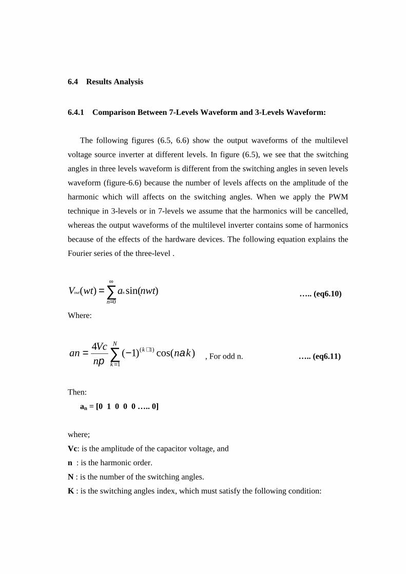
٧٥
6.4 Results Analysis
6.4.1 Comparison Between 7-Levels Waveform and 3-Levels Waveform:
The following figures (6.5, 6.6) show the output waveforms of the multilevel
voltage source inverter at different levels. In figure (6.5), we see that the switching
angles in three levels waveform is different from the switching angles in seven levels
waveform (figure-6.6) because the number of levels affects on the amplitude of the
harmonic which will affects on the switching angles. When we apply the PWM
technique in 3-levels or in 7-levels we assume that the harmonics will be cancelled,
whereas the output waveforms of the multilevel inverter contains some of harmonics
because of the effects of the hardware devices. The following equation explains the
Fourier series of the three-level .
0
)sin()(n
nwtawtV nout ….. (eq6.10)
Where:
N
k
k knn
Vcan
1
)1( )cos()1(4
, For odd n. ….. (eq6.11)
Then:
an = [0 1 0 0 0 ….. 0]
where;
Vc: is the amplitude of the capacitor voltage, and
n : is the harmonic order.
N : is the number of the switching angles.
K : is the switching angles index, which must satisfy the following condition:

٧٦
1< 2 < 3 … N <2
The corresponding harmonic amplitude matrix:
hn = [0Vc4
0 0 …. 0]
By using MATLAB program to solve the switching angle through Newton
Raphson method, the final results of iteration for 7-levels and 3-levels as in the
following table.
Table-6.2(Switching angle at seven level and three level)
7-Levels 3-Levels
1 5.9° 22.58o
2 14.8° 33.60o
3 25.2° 46.64o
4 33.1° 68.49o
5 ___ 75.09o
6 37.6° ___
7 41.5° ___
8 46° ___
9 51.2° ___
10 ___ ___
11 57.7° ___
12 66.7° ___
13 70.8° ___
14 75.2° ___
15 87.6° ___

٧٧
Figure-6.5(Three-level PWM waveform)
Figure-6.6(Seven-level PWM waveform)
6.4.2 Phase Waveforms Analysis:
The following figure (6.7) shows the output waveform of the multilevel inverter
at small values of frequency. As we know, by applying the PWM technique we can
get a waveform with small harmonics, but at large values of frequency, the PWM
technique can’t be applied as well as to get switching angles to cancel the harmonics
because the duty cycle of the E-MOSFETs is very small, so, the output waveform is
nearly like as a stepped waveform. These waveforms can’t be applied to AC load
because the values of voltages for each step are above the zero level.

٧٨
Figure-6.7(Phase waveform at different frequency (7-levels))
6.4.3 Phase-to-Phase Waveforms Analysis:
By getting the waveforms between two phases (figure-6.8), we see that it is
similar to the sinusoidal waveform with some of harmonics. Here, we see that the
average voltage of this waveform is zero. This signal is suitable to run any AC load
because there is a reference (zero) level with levels of voltages above this level and
another levels under this level, whereas the phase waveform does not have this
property.
Figure-6.8(Phase-to-Phase waveform at different frequency (7-levels))

٧٩
6.4.4 Waveform Analysis Using the Capacitors as DC-Link:
The following figures (6.9, 6.10) show the phase-to-phase and phase waveforms.
Here, we see that the waveforms is similar to the previous waveforms when we using
the batteries, but when we use the capacitors we see that there is unbalancing in the
distribution of the voltage at each capacitors ( Vdc/6 at each capacitor). This
unbalancing problem occurs because at the beginning (zero level) each capacitor will
has a voltage equal to Vdc/6, then by running the power circuit as a step, the
distribution of the DC voltage will change i.e. the lower levels which participate in
more steps will have the lowest voltage in comparison with the upper levels. For
example, C1 participates in every level except level zero, so it has the lowest voltage.
Whereas C6 participates only in level seven, so it has the largest value of voltage.
Figure-6.9(Phase-to-Phase waveform when using the capacitors)
Figure-6.10(Phase waveform when using the capacitors)

٨٠
CHAPTER SEVEN
CONCLUSION AND FUTURE WORK
7.1 Conclusion
7.2 Future Work

٨١
CHAPTER SEVEN
CONCLUSION AND FUTURE WORK
7.1 Conclusion:
One method of Controlling of speed of AC motor is the frequency converter,
which allows variable frequency and voltage supply to be obtained from a fixed
voltage and frequency AC supply. In this project there are three parts, the first is the
six pulse controlled rectifier which is used to control of the voltage by controlling the
firing angle, so this kind of rectifier will provide us a wide range of variable voltage.
Also it has a high efficiency (99%) and small ripple factor (3.1%) for small value of
firing angle (α=0), so the output power is high. The second part is the DC-Link,
which is consisting of capacitors that will provide a number of levels of voltages,
also by using the capacitors the losses, will be small because the equivalent series
resistance of each capacitor is very small. The third part is the seven level diode
clamped inverter, which is used to control of the frequency. In this kind of inverter
the harmonics will decrease as the numbers of levels increase, for example the THD
of 81 levels is less than 1%, but in seven levels the THD is greater than 10%. Also
increasing the number of switching angles (PWM technique) can reduce THD of the
line voltage.
In this project the output waveforms of frequency converter are nearly similar to
the sinusoidal waveform with some harmonic because we can’t apply the PWM
technique as well as to give no harmonic because of the hardware limitations as the
duty cycle of E-MOSFET, which affects on the waveforms and the output frequency.

٨٢
The most difficult problem that we faced in building the project was the
technique of isolation between the power circuit and the control circuit and to isolate
the gate of each E-MOSFET from the other.
7.2 Future Work:
In this project we deal with the open loop speed control of induction motor,
which requires a constant ratio between the voltage and the frequency. In the future
projects, we advise the researchers to build a closed loop speed control by using the
personal computer to control of the voltage. Also, in this project we can get a
maximum frequency nearly equal to 37 Hz, so in the future projects we hope to
increase this frequency above the rated value by using more suitable hardware
devices (power MOSFET), with more active isolation.

٨٣
References:
1. Dubey - "Fundamentals of Electrical Drives"- 2nd edition - Narosa Publishing
House - 1995.
2. Malvino - "electronic principles" - 6th edition- Glencoe McGraw_Hill - 1999.
3. William stalling - "computer organization and architecture"- 4th edition.
4. Rashid - "power electronics and applications"- 5th edition.
5. Nabac- I. Takahashi, "A New Neutral-Point-Clamped PWM Inverter"- 1998.
6. Leon M. Tolbert, Thomas G. Habetler- "Novel Multilevel Inverter Carrier-
Based PWM Methods"- IEEE IAS 1998 Annual Meeting- St. Louis,
Missouri- October -1998, p.1.
7. Fang, Z. Peng-"Multilevel Converters for Large Electric Drives"- 2000.
8. J. Sun- H. Grotstollen- “Solving Nonlinear Equations for Selective Harmonic
Eliminated PWM Using Predicted Initial Values-” Proc. IECON 1992-
pp.259-264.
9. Siriroj Sirisukprasert- "OPTIMIZED HARMONIC STEPPED-WAVEFORM
FOR MULTILEVEL INVERTER"- Bradley Department of Electrical and
Computer Engineering at Virginia Tech- January 1997.

٨٤
Appendix A
SOFTWARE ANALYSIS

٨٥
The following programs are used in analysis:
1. M-file used to solve the switching angles of optimized harmonic stepped-waveform is presented as follows:
Solve switching angle of 7-level OHSW by using the Newton-Raphson method.
E=6; %the number of dc sources or capacitors.
dM=0.001; %The modulation index step
Mstart=1.0; %The initial modulation index
M=Mstart*E;
Mrange=1000; %Range of calculation results
p1=4*pi/180;p2=8*pi/180;p3=11*pi/180;p4=19*pi/180;p6=35*pi/180;p7=40*pi/180;
p8=45*pi/180;p9=49*pi/180;p11=65*pi/180;p12=71*pi/180;p13=74*pi/180;p14=77*pi/180;
p15=80*pi/180;% Guess initial value of switching angles
p=[p1 p2 p3 p4 p6 p7 p8 p9 p11 p12 p13 p14 p15]'; %The switching angle matrix
for j=1:Mrange
t=[M*pi/4 0 0 0 0]'; %The corresponding harmonic amplitude matrix
df=1; i=1;
while abs(df) > 1e-20 & i < 40 %i=40 %Degree of accuracy condition
p1=p(1,:); p2=p(2,:); p3=p(3,:); p4=p(4,:); p6=p(5,:); p7=p(6,:); p8=p(7,:); p9=p(8,:); p11=p(9,:);
p12=p(10,:); p13=p(11,:); p14=p(12,:); p15=p(13,:);
f=[cos(p1)+cos(p2)+cos(p3)+cos(p4)+1.5cos(p6)+cos(p7)+cos(p8)+cos(p9)+1.5cos(p11)+cos(
p12) +cos(p13)+cos(p14)+cos(p15);
cos(5*p1)+cos(5*p2)+cos(5*p3)+cos(5*p4)+1.5cos(5*p6)+cos(5*p7)+cos(5*p8)+cos(5*p9)+
1.5cos(5*p11)+cos(5*p12) +cos(5*p13)+cos(5*p14)+cos(5*p15);
cos(7*p1)+cos(7*p2)+cos(7*p3)+cos(7*p4)+1.5cos(7*p6)+cos(7*p7)+cos(7*p8)+cos(7*p9)+
1.5cos(7*p11)+cos(7*p12) +cos(7*p13)+cos(7*p14)+cos(7*p15);
cos(11*p1)+cos(11*p2)+cos(11*p3)+cos(11*p4)+1.5cos(11*p6)+cos(11*p7)+cos(11*p8)+cos(11
*p9)+ 1.5cos(11*p11)+cos(11*p12) +cos(11*p13)+cos(11*p14)+cos(11*p15);
cos(13*p1)+cos(13*p2)+cos(13*p3)+cos(13*p4)+1.5cos(13*p6)+cos(13*p7)+cos(13*p8)+cos(13
*p9)+ 1.5cos(13*p11)+cos(13*p12) +cos(13*p13)+cos(13*p14)+cos(13*p15);
cos(17*p1)+cos(17*p2)+cos(17*p3)+cos(17*p4)+1.5cos(17*p6)+cos(17*p7)+cos(17*p8)+
cos(17*p9)+ 1.5cos(17*p11)+cos(17*p12) +cos(17*p13)+cos(17*p14)+cos(17*p15);

٨٦
cos(19*p1)+cos(19*p2)+cos(19*p3)+cos(19*p4)+1.5cos(19*p6)+cos(19*p7)+cos(19*p8)+cos(19
*p9)+ 1.5cos(19*p11)+cos(19*p12) +cos(19*p13)+cos(p19*14)+cos(p19*15);
cos(23*p1)+cos(23*p2)+cos(23*p3)+cos(23*p4)+1.5cos(23*p6)+cos(23*p7)+cos(23*p8)+cos(23
*p9)+ 1.5cos(23*p11)+cos(23*p12) +cos(23*p13)+cos(p3*p14)+cos(23*p15);
cos(25*p1)+cos(25*p2)+cos(25*p3)+cos(25*p4)+1.5cos(25*p6)+cos(25*p7)+cos(25*p8)+cos(25
*p9)+ 1.5cos(25*p11)+cos(25*p12) +cos(25*p13)+cos(25*p14)+cos(25*p15);
cos(29*p1)+cos(29*p2)+cos(29*p3)+cos(29*p4)+1.5cos(29*p6)+cos(29*p7)+cos(29*p8)+cos(29
*p9)+ 1.5cos(29*p11)+cos(29*p12) +cos(29*p13)+cos(29*p14)+cos(29*p15);
cos(31*p1)+cos(31*p2)+cos(31*p3)+cos(31*p4)+1.5cos(31*p6)+cos(31*p7)+cos(31*p8)+cos(31
*p9)+ 1.5cos(31*p11)+cos(31*p12) +cos(31*p13)+cos(31*p14)+cos(31*p15);
cos(33*p1)+cos(33*p2)+cos(33*p3)+cos(33*p4)+1.5cos(33*p6)+cos(33*p7)+cos(33*p8)+cos(33
*p9)+ 1.5cos(33*p11)+cos(33*p12) +cos(33*p13)+cos(33*p14)+cos(33*p15);
cos(35*p1)+cos(35*p2)+cos(35*p3)+cos(35*p4)+1.5cos(35*p6)+cos(35*p7)+cos(35*p8)+cos(35
*p9)+ 1.5cos(35*p11)+cos(35*p12) +cos(35*p13)+cos(35*p14)+cos(35*p15)];
delf=[-sin(p1),-sin(p2),-sin(p3),-sin(p4),-1.5sin(p6),-sin(p7),-sin(p8),-sin(p9),-1.5sin(p11),-sin(p12),
-sin(p13) ,-sin(p14) ,-sin(p15);
-5*sin(5*p1),-5*sin(5*p2),-5*sin(5*p3),-5*sin(5*p4),-7.5*sin(5*p6),-5*sin(5*p7),-5*sin(5*p8),
-5*sin(5*p9),-7.5*sin(5*p11),-5*sin(5*p12),-5*sin(5*p13),-5*sin(5*p14), -5*sin(5*p15);
-7*sin(7*p1),-7*sin(7*p2),-7*sin(7*p3),-7*sin(7*p4),-10.5*sin(7*p6),-7*sin(7*p7),-7*sin(7*p8),
-7*sin(7*p9), -10.5*sin(7*p11), -7*sin(7*p12) ,-7*sin(7*p13), -7*sin(7*p14), -7*sin(7*p15);
-11*sin(11*p1),-11*sin(11*p2),-11*sin(11*p3),-11*sin(11*p4),-16.5*sin(11*p6),-11*sin(11*p7),
-11*sin(11*p8),-11*sin(11*p9),-16.5*sin(11*p11),-11*sin(11*p12),-11*sin(11*p13),-
11*sin(11*p14), -11*sin(11*p15);
-13*sin(13*p1),-13*sin(13*p2),-13*sin(13*p3),-13*sin(13*p4),-13*sin(19.5*p6),-13*sin(13*p7),
-13*sin(13*p8),-13*sin(13*p9),-19.5*sin(13*p11),-13*sin(13*p12),-13*sin(13*p13),-13*sin(13*p14),
-13*sin(13*p15);
-17*sin(17*p1),-17*sin(17*p2),-17*sin(17*p3),-17*sin(17*p4),-17*sin(17*p6), -25.5*sin(17*p7),
-17*sin(17*p8),-17*sin(17*p9),-25.5*sin(17*p11),-17*sin(17*p12),-17*sin(17*p13),-17*sin(17*p14),
-17*sin(17*p15);
-19*sin(19*p1),-19*sin(19*p2),-19*sin(19*p3),-19*sin(19*p4),-28.5*sin(19*p6),-19*sin(19*p7),
-19*sin(19*p8),-19*sin(19*p9),-28.5*sin(19*p11),-19*sin(19*p12),-19*sin(19*p13),-19*sin(19*p14),
-19*sin(19*p15);
-23*sin(23*p1),-23*sin(23*p2),-23*sin(23*p3),-23*sin(23*p4),-34.5*sin(23*p6), -23*sin(23*p7),
-23*sin(23*p8),-23*sin(23*p9),-34.5*sin(23*p11),-23*sin(23*p12),-23*sin(23*p13),-23*sin(23*p14),

٨٧
-23*sin(23*p15);
-25*sin(25*p1),-25*sin(25*p2),-25*sin(25*p3),-25*sin(25*p4),-37.5*sin(25*p6),-25*sin(25*p7),
-25*sin(25*p8),-25*sin(25*p9),-37.5*sin(25*p11),-25*sin(25*p12),-25*sin(25*p13),-25*sin(25*p14),
-25*sin(25*p15);
-29*sin(29*p1),-29*sin(29*p2),-29*sin(29*p3),-29*sin(29*p4),-34.5*sin(29*p6),-29*sin(29*p7),
-29*sin(29*p8),-29*sin(29*p9),-34.5*sin(29*p11),-29*sin(29*p12),-29*sin(29*p13),-29*sin(29*p14),
-29*sin(29*p15);
-31*sin(31*p1),-31*sin(31*p2),-31*sin(31*p3),-31*sin(31*p4),-46.5*sin(31*p6),-31*sin(31*p7),
-31*sin(31*p8),-31*sin(31*p9),-46.5*sin(31*p11),-31*sin(31*p12),-31*sin(31*p13),-31*sin(31*p14),
-31*sin(31*p15);
-33*sin(33*p1),-33*sin(33*p2),-33*sin(33*p3),-33*sin(33*p4),-49.5*sin(33*p6),-33*sin(33*p7),
-33*sin(33*p8),-33*sin(33*p9),-49.5*sin(33*p11),-33*sin(33*p12),-33*sin(33*p13), -33*sin(33*p14),
-33*sin(33*p15);
-35*sin(35*p1),-35*sin(35*p2),-35*sin(35*p3),-35*sin(35*p4),-52.5*sin(35*p6),-35*sin(35*p7),
-35*sin(35*p8),-35*sin(35*p9),-52.5*sin(35*p11),-35*sin(35*p12),-35*sin(35*p13),-35*sin(35*p14),
-35*sin(35*p15) ];% The differential matrix
df=inv(delf)*(t-f); % Calculate solution error
p=p+df; % Update the solutions.
i=i+1;
end
mm(j)=M/E; % The modulation index
M=M-dM; %Update the modulation index
End; % End of File
2. The following program illustrate the relationship between the frequency (f) and thetriggering angle (a) %
a=[0:1:90]B1=5f1=315.25*cos(a*pi/180)/B1B2=6.305f2=315.25*cos(a*pi/180)/B2B3=7f3=315.25*cos(a*pi/180)/B3
plot(a,f1,'--',a,f2,'-',a,f3,':')xlabel('a (degree)')ylabel('f (Hz)')

٨٨
3. The following program illustrate the relationship between the Ripple Factor and thetriggering angle (a) %
a=[0:1:80]
R=(pi*pi*(0.5+(3*sqrt(3)/(4*pi))*(cos(2*a*pi/180))))
b=9*cos(a*pi/180).*cos(a*pi/180)
c=100*(sqrt((R./b)-1))
plot(a,c,'-')
xlabel('a (degree)')ylabel('R.F.(%)')

٨٩
Appendix B
Visual Basic Program

٩٠
' This program is used to run the Induction motor at any required speed.
' The following program deal with output signals at the parallel port.
' In the form of the program the user must enter the correct values of motor parameters.
' Then the user enters the demand parameters.
' Click on the Required Voltage bottom to determine the value of the required voltage.
' Click on the RUN bottom to run the motor.
' Click on the STOP bottom to stop the motor.
' Click on EXIT bottom to exit from the program.
Option Explicit
Dim p, n, f, B, v, x, t, i, time As Double
Dim s As Boolean
Dim strNo As String
Dim res() As String
Private Sub Command1_Click()
Dim temp1 As Double
temp1 = x * 10000
strNo = Str(temp1)
res = Split(strNo, ".")
temp1 = Val(res(0))
Print temp1
s = True
Text9.Text = Val(time)
'Timer1.Interval = time
'Timer1.Enabled = True
While s = True
Call vbOut(888, 96)

٩١
Call vbOut(890, 0)
For i = 0 To temp1
Next
Call vbOut(888, 153)
Call vbOut(890, 0)
For i = 0 To temp1
Next
Call vbOut(888, 146)
Call vbOut(890, 0)
For i = 0 To temp1
Next
Call vbOut(888, 75)
Call vbOut(890, 0)
For i = 0 To temp1
Next
Call vbOut(888, 4)
Call vbOut(890, 0)
For i = 0 To temp1
Next
Call vbOut(888, 197)
Call vbOut(890, 2)
For i = 0 To temp1
Next

٩٢
Call vbOut(888, 142)
Call vbOut(890, 2)
For i = 0 To temp1
Next
Call vbOut(888, 86)
Call vbOut(890, 2)
For i = 0 To temp1
Next
Call vbOut(888, 29)
Call vbOut(890, 2)
For i = 0 To temp1
Next
Call vbOut(888, 36)
Call vbOut(890, 2)
For i = 0 To temp1
Next
Call vbOut(888, 107)
Call vbOut(890, 2)
For i = 0 To temp1
Next
Call vbOut(888, 178)
Call vbOut(890, 2)
For i = 0 To temp1
Next

٩٣
Call vbOut(888, 241)
Call vbOut(890, 2)
For i = 0 To temp1
Next
Call vbOut(888, 40)
Call vbOut(890, 0)
For i = 0 To temp1
Next
Wend
End Sub
Private Sub Command2_Click()
p = Val(Text6.Text) 'NO. of pole
n = Val(Text7.Text) 'Speed (rpm)
B = Val(Text8.Text) 'v/f(V/Hz)
f = (p * n) / 120 'Frequency
v = B * f
t = 1 / f 'period
x = (t / 14) * 1000 'trigger time
If (v >= Val(Text1.Text)) Then
MsgBox "Enter the correct value ", vbOKOnly, "Error value"
Else
Text10.Text = Val(v)

٩٤
End If
End Sub
Private Sub Command3_Click()
Call vbOut(888, 0)
Call vbOut(890, 2)
End Sub
Private Sub Command4_Click()
End
End Sub
Private Sub Form_Load()
Text1.Text = ""
Text2.Text = ""
Text3.Text = ""
Text4.Text = ""
Text5.Text = ""
Text6.Text = ""
Text7.Text = ""
Text8.Text = ""
Text9.Text = ""
Text10.Text = ""
End Sub

٩٥
Private Sub Text3_Change()
If (Val(Text3.Text) > 2000) Then
MsgBox (" The Power must be less than 2000")
End If
End Sub
Private Sub Text4_LostFocus()
If (Text4.Text <> "") Then
If (Val(Text4.Text) >= 1 Or Val(Text4.Text) <= 0.6) Then
MsgBox "The Power Factor must be less than 1 and greater than 0.6", vbOKOnly, "Error Power
Factor Value"
End If
End If
End Sub
Private Sub Text6_Change()
If (Val(Text6.Text) = 2) And (Val(Text7.Text) > 2100) Then
MsgBox "The speed value must be less than 2100", vbOKOnly, "Error Value"
End If
If (Val(Text6.Text) = 4) And (Val(Text7.Text) > 1050) Then
MsgBox "The speed value must be less than 1050", vbOKOnly, "Error Value"
End If
End Sub
Private Sub Text7_Change()
If ((Text7.Text) <> "") Then
If (Val(Text7.Text) > Val(Text5.Text)) Then
MsgBox "The speed value must be less than or equale the rated ", vbOKOnly, "Error Value"
End If
End If

٩٦
If (Val(Text6.Text) = 2) And (Val(Text7.Text) > 2100) Then
MsgBox "The speed value must be less than 2100", vbOKOnly, "Error Value"
End If
If (Val(Text6.Text) = 4) And (Val(Text7.Text) > 1050) Then
MsgBox "The speed value must be less than 1050", vbOKOnly, "Error Value"
End If
End Sub

٩٧
Appendix C
DATA SHEETS

٩٨

٩٩

١٠٠

١٠١

١٠٢

١٠٣

١٠٤
١٠٥

١٠٦

١٠٧

١٠٨

١٠٩

١١٠

١١١

١١٢

١١٣
١١٤

١١٥
High Power Heat SinksMany specialized types of semiconductor devicesoperate at the very high power density levels andrequire a more engineered and intense thermal solution.Some examples of these very high power density /generating semiconductor devices are:
Rectifier Devices (e.g. Phase ControlThyristors and Diodes)
Medium Voltage Thyristors (e.g. PowerSwitches)
Fast Switching Devices (e.g. Fast Turn-offThyristors and Fast Recovery Diodes)
IGBT's including Gate Controlled Devices,GTO Thyristors
The industrial use of these products is quite versatile. Industries engaged in the manufacturing ofelectric vehicles, telecommunications, military, aerospace, welding equipment, motor controls, tractiondrive, and HVDC require a cooling solution specific to each design and ultimate power dissipation.
ThermaFlo develops efficient cooling solution for these industries using a methodology of applyingstandard product manufacturing technology and know-how towards developing a cooling solution forcooling high power electronics.
Some of the technologies that ThermaFlo uses in developing high power electronics cooling systemsare:
Extremely High Aspect Ratio Heat sink Extrusions Folded Fin Heat sink Technology Bonded Fin Heat sink Technology High Mass and Surface Area Extruded Heat sink Copper Heat sinks Integrated Heat Pipe and Heat Sink Solutions
To learn more about these and other technologies that can be used for developing high power coolingsolutions, please contact ThermaFlo's Engineering Department today.