Uyemura Customer Builds America's First PCB Shop in 15 Yrs
8
China and Korea are today’s LCC (Low Cost Country) manufacturers for PC boards of all types. In 2012, Whelen Engineering (Chester, CT and Charlestown, NH) was among the tens of thousands of OEMs that sourced their PCBs from Asia. Then, a perfect storm of intellectual property issues, lengthening lead times and increasing cost led the company to build - greenfield and-in-house – America’s first new rigid PCB shop in 15 years. Whelen Engineering is a leading manufacturer of safety lighting and sirens for automotive, aviation and emergency warning applications. Their about-face in how they source the brains for every product they sell tells an important story about the power of innovation, the merits of questioning common wisdom, and how both of these can generate a Proof of Concept with implications far beyond one manufacturing operation. Whelen was founded (in 1952) on the pillars of advanced production equipment, a motivated An Interview with John Meyers, UIC's new Strategic Accounts Manager Q: You are known for your expertise with ENIG. How would you differentiate the Uyemura product from others in the market? A. The process cost for nickel plating can be as much as twice as high when dummy plating is required after downtime or to meet minimum loading requirements. Deactivation of most nickel baths can occur in less than 2 hours. At this point, dummy plating becomes necessary, which increases costs dramatically by using much more chemistry and labor. (continued on pg. 6) (continued on pg. 2) UIC Customer Builds America’s First New Rigid PCB Shop in 15 Years Proof of Concept shows ability to out-compete Asia on direct PCB price per sq. in.
-
Upload
khangminh22 -
Category
Documents
-
view
0 -
download
0
Transcript of Uyemura Customer Builds America's First PCB Shop in 15 Yrs

The production ramp is underway and expected to be completed shortly whereupon, Whelen Engi-neering will have 100% of its PCB production back in the USA – and bragging rights about achieving substantial cost savings over PCBs from China. “That includes both direct and indirect costs, as well as massive savings in cycle time,” says Stepinski. “We expect to be the first shop in the west to out-compete the Asia-Pacific region on direct PCB price per square inch.”
It is also the first totally “green” pcb shop. Explains Stepinski, “there is no need for wastewater permits, or air permits; liquid is 100% recycled, and we designed-out all of the air toxics.” A non-regulated resist stripper was developed as well. “We use just 500 gallons of fresh water a day to compensate for humidity loss from our air scrubber (which runs on recycled DI water to maximize absorption efficiency), and we have the first in the world, closed
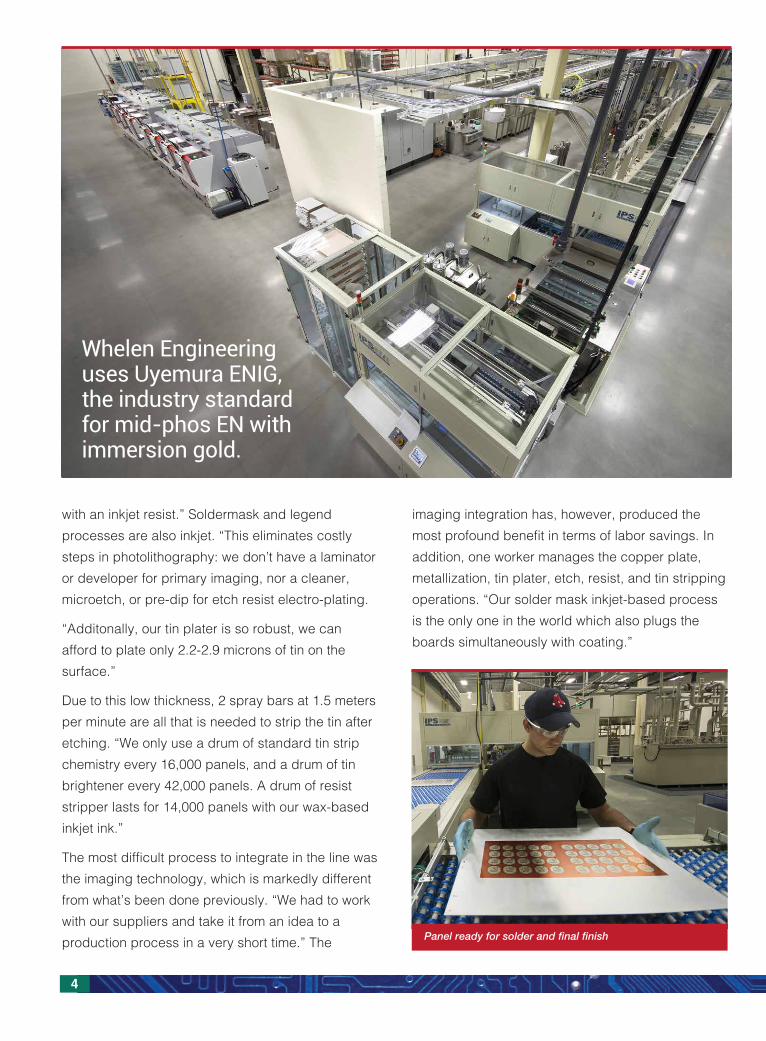
imaging integration has, however, produced the most profound benefit in terms of labor savings. In addition, one worker manages the copper plate, metallization, tin plater, etch, resist, and tin stripping operations. “Our solder mask inkjet-based process is the only one in the world which also plugs the boards simultaneously with coating.”
China and Korea are today’s LCC (Low Cost Country) manufacturers for PC boards of all types.
In 2012, Whelen Engineering (Chester, CT and Charlestown, NH) was among the tens of thousands of OEMs that sourced their PCBs from Asia. Then, a perfect storm of intellectual property issues, lengthening lead times and increasing cost led the company to build - greenfield and-in-house – America’s first new rigid PCB shop in 15 years.
Whelen Engineering is a leading manufacturer of safety lighting and sirens for automotive, aviation and emergency warning applications. Their about-face in how they source the brains for every product they sell tells an important story about the power of innovation, the merits of questioning common wisdom, and how both of these can generate a Proof of Concept with implications far beyond one manufacturing operation.
Whelen was founded (in 1952) on the pillars of advanced production equipment, a motivated
workforce, and a commitment to vertical manufac-turing initiatives. In 2012, the company’s visionary CEO, John Olson, launched a new project that would take that vertical integration to an entirely new level.
“We also wanted an ROI of no more than 5 years, and although the industry minimum average headcount for a facility of this scale is 100 workers, we wanted to achieve everything with a workforce of no more than 17 total employees.”
Stepinski completed his initial design/business plan in 6 weeks: a unique U-shaped configuration 550’ long, with a 4.5 hour cycle time on a 50,000 sq-ft overall footprint.
A 2-level command center is elevated 12’ above the line. The first level is a chem lab, where one technician does wet process and cross-sectional analysis testing for the entire facility, in 6 hours per day. Both levels also house banks of monitors that track the temperature, concentration and level of every chemical, and the progress of each order. The line uses 39 pieces of automation linking 24 value-added process steps.
“We are really focused on lean concepts of waste reduction,” Stepinski continues. “Chemistry is stored in vented day tanks, with sensors monitoring levels and checking for leaks. Live inventory data is
database, pulling information relevant for that job, and processes it, from deburr thru final finish, in 4.5 hours and reports. Location/status is reported in real time via hundreds of its in-line sensors. “There is a 3% max coefficient of variation in plated surface copper thickness; the etch sytem has a maximum 1.5% variation in etch rate. This consistency allows us to run just one plating recipe, and one etching recipe, throughout the factory.”
The only stage where recipes change is in the imaging equipment. “This imaging equipment is first in the world, all digital inkjet technology,” says Stepinski. “We do digital inkjet printing for print and etch of the inner layers and metal core products, as well as for plate and etch of the outerlayers. For plate and etch, we panel plate all outerlayers and subcomposites with horizontal copper plating; however, we then tin plate the final etch resist so we have a ‘plate and etch’ process
with an inkjet resist.” Soldermask and legend processes are also inkjet. “This eliminates costly steps in photolithography: we don’t have a laminator or developer for primary imaging, nor a cleaner, microetch, or pre-dip for etch resist electro-plating.
“Additonally, our tin plater is so robust, we can afford to plate only 2.2-2.9 microns of tin on the surface.”
Due to this low thickness, 2 spray bars at 1.5 meters per minute are all that is needed to strip the tin after etching. “We only use a drum of standard tin strip chemistry every 16,000 panels, and a drum of tin brightener every 42,000 panels. A drum of resist stripper lasts for 14,000 panels with our wax-based inkjet ink.”
The most difficult process to integrate in the line was the imaging technology, which is markedly different from what’s been done previously. “We had to work with our suppliers and take it from an idea to a production process in a very short time.” The
A thorough analysis of current product designs and roadmap tolerance requirements was used to establish process spec targets.
“Extensive experimentation with large quantities of test panels was also required to adjust the plating thickness variation to the required level across our entire product mix. But by designing it all up-front, and systematically qualifying it, we now have a robust, predictable, low maintenance process for many years to come.”
Process controls were qualified to the point that no test panels are needed to interrupt production to qualify different product recipes, nor are any dummy panels required to compensate for current density edge effects. Whelen’s metallization process is “green” and based upon conductive polymer.
An Interview withJohn Meyers,UIC's new Strategic Accounts Manager
Q: You are known for your expertise with ENIG. How would you differentiate the Uyemura product from others in the market?
A. The process cost for nickel plating can be as
much as twice as high when dummy plating is
required after downtime or to meet minimum
loading requirements. Deactivation of most
nickel baths can occur in less than 2 hours. At
this point, dummy plating becomes necessary,
which increases costs dramatically by using
much more chemistry and labor.
Dummy plating has effectively been made obsolete
with UIC’s ENIG. The UIC process, in fact, does not
'deactivate' at all. The first basket of panels
processed after many hours or even a full day, can
be live production parts.
The second differentiator involves minimum load
factor. Whether you're running gold afterwards, or
ENEPIG, you can run one 3" X 4” coupon or a full
basket of 18" X 24" panels in (UIC’s) NPR-4
electroless nickel, and the Ni plated thickness will be
identical. When users of competitors‘ chemistry
have a small area 'hot job,' more square footage of
work is required per gallon of solution for the bath to
perform properly.
Control of the bath is also key. Uyemura Japan and
Uyemura USA have a controller (STARLiNE-DASH®
4-NP) that is phenomenal. The DASH 4-NP samples
the EN plating solution, cools it, analyzes all the
components, including pH values, and replenishes
automatically. As a result, baths can be maintained
continuously at 2-4% of optimum; nickel can be
controlled within +/-0.05 g/L.
Q. What about the issue of turnovers?
A. As nickel baths age from 0 to 5 metal turnovers, the
plating rate slows down. Virtually everyone dumps
the bath at 5 MTO, or does a transfer-nitric clean-
ing-return procedure. The problem with competitors’
baths is as the nickel plating rate goes down,
additional process changes are required to
compensate for it. Our controller compensates for
metal turnovers and adjusts the components
automatically. So, at 1, or 3 - or 5 MTOs, there's zero
difference in plated results.
Finally, the UIC nickel bath gets points for stability.
Five months in, look in the tank and see how much
nickel plated out in any competitor’s bath. With
ours, the amount is substantially less. Plate-out is
a huge waste of material, and the nitric stripping
required to eliminate it produces hazardous waste.
The bottom line with ENIG is you want gold
deposition with perfect uniformity. We control the
phosphorus content in the nickel bath at 6-8% so
that gold distribution is exactly that: perfectly
uniform. Standards are met, and there are no
outliers - no isolated pads that needlessly get
more gold.
Two of the largest circuit board manufacturers in
North America – independent of each other -
compared 5 ENIG suppliers for corrosion and gold
distribution. UIC’s was first for gold uniformity on
isolated features, and for lowest corrosion.
(continued on pg. 6)
The system was designed so there’s no need to vent ammonia etch. “By performing the oxidation reaction offline in a separate sealed reactor, we’ve created a totally closed system.” Rinses are regenerated with a proprietary process as well. Virtually no hazwaste is generated (overall hazwaste volume as a stand-alone PCB shop meets the conditions of a small quantity generator, the company is regulated at a higher level).
Whelen was able to ‘design-out’ pollution concerns because the factory and waste treatment were a single, integrated design. “Our operating costs for waste treatment are far below conventional systems, and even our capital investment in waste treatment was below average for a shop our size” says Stepinski.
“There are practically no treatment chemicals used, except for minute amounts of acid and caustic. The high level of recycling that we do actually offsets most of the operating costs of our environmental systems. On a per-panel basis, conventional factories spend more money on fresh water than we spend on all of our combined regulatory operations.”
The manufacturing model developed for PCBs by Whelen Engineering is a Proof of Concept that’s applicable, in the company’s view, for many products. “The key,” says Stepinski, “is not just automation of a single piece of equipment, (in operations like drilling, plating, imaging, etc.), but
the combining of new technologies, such as inkjet and others, and the use of new, more efficient, more integrated process equipment.”
The Whelen model is a new solution that addresses this competitive advantage by engineering the integration of different processes to a new level of efficiency according to Stepinski. “The majority of the cost of quality in manufacturing boards is non-valued waste stemming from a lack of inter-process integration. This can be up to 80-90%
(continued on pg. 2)
UIC Customer Builds America’s FirstNew Rigid PCB Shop in 15 YearsProof of Concept shows ability to out-compete Asia on direct PCB price per sq. in.
of a typical shop’s labor costs, and essentially all of the regulatory costs.”
Whelen’s market share is 80% in the US; the company is also very strong in South America, Europe and the Middle East. “This is a smart, private company that takes the long view. As a result, it is
loop recycling system for ammonia etchant.” It covers every waste aspect of the system. “We plate the copper out of the etchant, and rather than ammonium chloride for etching, we use a cocktail of ammonium sulfate and other low cost generic compunds, which we developed in partnership with a supplier to plate out the copper.
“We sell the 99.9% pure copper to a local recycler, and do not add any fresh chemicals to the etcher (chemicals were only needed for initial makeup). Our plating chemistry supplier has even approved the copper quality from the etcher for reuse in the plater, which will allow us to take copper that is removed at etch to be redissolved in the plater.
“This reduced our overall raw copper purchases by 95%, and allowed us to metallize the circuit pattern using waste copper from the laminate.”
continuously available. Tanks are sized for 3X supply chain average lead time. Our day tank system also reduces the number of manual chemical transactions by 99% versus a conven-tional facility by eliminating the hazardous, labor-intensive manual adds from the partially used drums. All adds are made via an HMI interface controlling metering pumps with safety interlocks. Laminate, masks and other solid materials are also stored in highly visible locations, with no central inventory.”
At the start of production, drilled panels are placed in a tray, which is barcoded; the tray then pings the
“Everyone who comes through this plant sees it as the next step in the evolution of making PCBs,” he adds, “and a solid ‘Proof of Concept’ for efficiently making many other products as well.”
At the time, Whelen Engineering was spending millions of dollars each year on PCBs from China; prices and lead times were both on an upward trajectory. Injection molding and other critical operations had already been brought in-house, with results exceeding forecasts. A strategic decision was made to explore whether board making could be next.
In Spring 2013, management recruited Alex Stepinski, whose experience included senior engineering and management roles at large North American PCB Fab companies to develop a plan. He was, in his words, “all about nonconventional approaches.”
“The idea,” explains Stepinski, “was to build a fully
automated operation based on our core principles
that would produce a higher quality PWB, at a lower
price, with shorter lead times than offshore. The takt requirement to achieve 100% reshoring was PC board output of 50 panels per hour; translating to 2500 per week of 18” X 24” and 21” X 24”, rigid and rigid-flex panels; with capacity to expand up to 10,000 panels per week over the next decade.
able to make substantial multi-year investments without having to defend itself against shareholders hungry for the next quarterly guidance.”

The production ramp is underway and expected to be completed shortly whereupon, Whelen Engi-neering will have 100% of its PCB production back in the USA – and bragging rights about achieving substantial cost savings over PCBs from China. “That includes both direct and indirect costs, as well as massive savings in cycle time,” says Stepinski. “We expect to be the first shop in the west to out-compete the Asia-Pacific region on direct PCB price per square inch.”
It is also the first totally “green” pcb shop. Explains Stepinski, “there is no need for wastewater permits, or air permits; liquid is 100% recycled, and we designed-out all of the air toxics.” A non-regulated resist stripper was developed as well. “We use just 500 gallons of fresh water a day to compensate for humidity loss from our air scrubber (which runs on recycled DI water to maximize absorption efficiency), and we have the first in the world, closed
imaging integration has, however, produced the most profound benefit in terms of labor savings. In addition, one worker manages the copper plate, metallization, tin plater, etch, resist, and tin stripping operations. “Our solder mask inkjet-based process is the only one in the world which also plugs the boards simultaneously with coating.”
China and Korea are today’s LCC (Low Cost Country) manufacturers for PC boards of all types.
In 2012, Whelen Engineering (Chester, CT and Charlestown, NH) was among the tens of thousands of OEMs that sourced their PCBs from Asia. Then, a perfect storm of intellectual property issues, lengthening lead times and increasing cost led the company to build - greenfield and-in-house – America’s first new rigid PCB shop in 15 years.
Whelen Engineering is a leading manufacturer of safety lighting and sirens for automotive, aviation and emergency warning applications. Their about-face in how they source the brains for every product they sell tells an important story about the power of innovation, the merits of questioning common wisdom, and how both of these can generate a Proof of Concept with implications far beyond one manufacturing operation.
Whelen was founded (in 1952) on the pillars of advanced production equipment, a motivated
workforce, and a commitment to vertical manufac-turing initiatives. In 2012, the company’s visionary CEO, John Olson, launched a new project that would take that vertical integration to an entirely new level.
“We also wanted an ROI of no more than 5 years, and although the industry minimum average headcount for a facility of this scale is 100 workers, we wanted to achieve everything with a workforce of no more than 17 total employees.”
Stepinski completed his initial design/business plan in 6 weeks: a unique U-shaped configuration 550’ long, with a 4.5 hour cycle time on a 50,000 sq-ft overall footprint.
A 2-level command center is elevated 12’ above the line. The first level is a chem lab, where one technician does wet process and cross-sectional analysis testing for the entire facility, in 6 hours per day. Both levels also house banks of monitors that track the temperature, concentration and level of every chemical, and the progress of each order. The line uses 39 pieces of automation linking 24 value-added process steps.
“We are really focused on lean concepts of waste reduction,” Stepinski continues. “Chemistry is stored in vented day tanks, with sensors monitoring levels and checking for leaks. Live inventory data is
database, pulling information relevant for that job, and processes it, from deburr thru final finish, in 4.5 hours and reports. Location/status is reported in real time via hundreds of its in-line sensors. “There is a 3% max coefficient of variation in plated surface copper thickness; the etch sytem has a maximum 1.5% variation in etch rate. This consistency allows us to run just one plating recipe, and one etching recipe, throughout the factory.”
The only stage where recipes change is in the imaging equipment. “This imaging equipment is first in the world, all digital inkjet technology,” says Stepinski. “We do digital inkjet printing for print and etch of the inner layers and metal core products, as well as for plate and etch of the outerlayers. For plate and etch, we panel plate all outerlayers and subcomposites with horizontal copper plating; however, we then tin plate the final etch resist so we have a ‘plate and etch’ process
with an inkjet resist.” Soldermask and legend processes are also inkjet. “This eliminates costly steps in photolithography: we don’t have a laminator or developer for primary imaging, nor a cleaner, microetch, or pre-dip for etch resist electro-plating.
“Additonally, our tin plater is so robust, we can afford to plate only 2.2-2.9 microns of tin on the surface.”
Due to this low thickness, 2 spray bars at 1.5 meters per minute are all that is needed to strip the tin after etching. “We only use a drum of standard tin strip chemistry every 16,000 panels, and a drum of tin brightener every 42,000 panels. A drum of resist stripper lasts for 14,000 panels with our wax-based inkjet ink.”
The most difficult process to integrate in the line was the imaging technology, which is markedly different from what’s been done previously. “We had to work with our suppliers and take it from an idea to a production process in a very short time.” The
A thorough analysis of current product designs and roadmap tolerance requirements was used to establish process spec targets.
“Extensive experimentation with large quantities of test panels was also required to adjust the plating thickness variation to the required level across our entire product mix. But by designing it all up-front, and systematically qualifying it, we now have a robust, predictable, low maintenance process for many years to come.”
Process controls were qualified to the point that no test panels are needed to interrupt production to qualify different product recipes, nor are any dummy panels required to compensate for current density edge effects. Whelen’s metallization process is “green” and based upon conductive polymer.
Q: You are known for your expertise with ENIG. How would you differentiate the Uyemura product from others in the market?
A. The process cost for nickel plating can be as
much as twice as high when dummy plating is
required after downtime or to meet minimum
loading requirements. Deactivation of most
nickel baths can occur in less than 2 hours. At
this point, dummy plating becomes necessary,
which increases costs dramatically by using
much more chemistry and labor.
Dummy plating has effectively been made obsolete
with UIC’s ENIG. The UIC process, in fact, does not
'deactivate' at all. The first basket of panels
processed after many hours or even a full day, can
be live production parts.
The second differentiator involves minimum load
factor. Whether you're running gold afterwards, or
ENEPIG, you can run one 3" X 4” coupon or a full
basket of 18" X 24" panels in (UIC’s) NPR-4
electroless nickel, and the Ni plated thickness will be
identical. When users of competitors‘ chemistry
have a small area 'hot job,' more square footage of
work is required per gallon of solution for the bath to
perform properly.
Control of the bath is also key. Uyemura Japan and
Uyemura USA have a controller (STARLiNE-DASH®
4-NP) that is phenomenal. The DASH 4-NP samples
the EN plating solution, cools it, analyzes all the
components, including pH values, and replenishes
automatically. As a result, baths can be maintained
continuously at 2-4% of optimum; nickel can be
controlled within +/-0.05 g/L.
Q. What about the issue of turnovers?
A. As nickel baths age from 0 to 5 metal turnovers, the
plating rate slows down. Virtually everyone dumps
the bath at 5 MTO, or does a transfer-nitric clean-
ing-return procedure. The problem with competitors’
baths is as the nickel plating rate goes down,
additional process changes are required to
compensate for it. Our controller compensates for
metal turnovers and adjusts the components
automatically. So, at 1, or 3 - or 5 MTOs, there's zero
difference in plated results.
Finally, the UIC nickel bath gets points for stability.
Five months in, look in the tank and see how much
nickel plated out in any competitor’s bath. With
ours, the amount is substantially less. Plate-out is
a huge waste of material, and the nitric stripping
required to eliminate it produces hazardous waste.
The bottom line with ENIG is you want gold
deposition with perfect uniformity. We control the
phosphorus content in the nickel bath at 6-8% so
that gold distribution is exactly that: perfectly
uniform. Standards are met, and there are no
outliers - no isolated pads that needlessly get
more gold.
Two of the largest circuit board manufacturers in
North America – independent of each other -
compared 5 ENIG suppliers for corrosion and gold
distribution. UIC’s was first for gold uniformity on
isolated features, and for lowest corrosion.
The system was designed so there’s no need to vent ammonia etch. “By performing the oxidation reaction offline in a separate sealed reactor, we’ve created a totally closed system.” Rinses are regenerated with a proprietary process as well. Virtually no hazwaste is generated (overall hazwaste volume as a stand-alone PCB shop meets the conditions of a small quantity generator, the company is regulated at a higher level).
Whelen was able to ‘design-out’ pollution concerns because the factory and waste treatment were a single, integrated design. “Our operating costs for waste treatment are far below conventional systems, and even our capital investment in waste treatment was below average for a shop our size” says Stepinski.
“There are practically no treatment chemicals used, except for minute amounts of acid and caustic. The high level of recycling that we do actually offsets most of the operating costs of our environmental systems. On a per-panel basis, conventional factories spend more money on fresh water than we spend on all of our combined regulatory operations.”
The manufacturing model developed for PCBs by Whelen Engineering is a Proof of Concept that’s applicable, in the company’s view, for many products. “The key,” says Stepinski, “is not just automation of a single piece of equipment, (in operations like drilling, plating, imaging, etc.), but
the combining of new technologies, such as inkjet and others, and the use of new, more efficient, more integrated process equipment.”
The Whelen model is a new solution that addresses this competitive advantage by engineering the integration of different processes to a new level of efficiency according to Stepinski. “The majority of the cost of quality in manufacturing boards is non-valued waste stemming from a lack of inter-process integration. This can be up to 80-90%
Cassette-driven automatic load and unload drilling operation
of a typical shop’s labor costs, and essentially all of the regulatory costs.”
Whelen’s market share is 80% in the US; the company is also very strong in South America, Europe and the Middle East. “This is a smart, private company that takes the long view. As a result, it is
loop recycling system for ammonia etchant.” It covers every waste aspect of the system. “We plate the copper out of the etchant, and rather than ammonium chloride for etching, we use a cocktail of ammonium sulfate and other low cost generic compunds, which we developed in partnership with a supplier to plate out the copper.
“We sell the 99.9% pure copper to a local recycler, and do not add any fresh chemicals to the etcher (chemicals were only needed for initial makeup). Our plating chemistry supplier has even approved the copper quality from the etcher for reuse in the plater, which will allow us to take copper that is removed at etch to be redissolved in the plater.
“This reduced our overall raw copper purchases by 95%, and allowed us to metallize the circuit pattern using waste copper from the laminate.”
continuously available. Tanks are sized for 3X supply chain average lead time. Our day tank system also reduces the number of manual chemical transactions by 99% versus a conven-tional facility by eliminating the hazardous, labor-intensive manual adds from the partially used drums. All adds are made via an HMI interface controlling metering pumps with safety interlocks. Laminate, masks and other solid materials are also stored in highly visible locations, with no central inventory.”
At the start of production, drilled panels are placed in a tray, which is barcoded; the tray then pings the
“Everyone who comes through this plant sees it as the next step in the evolution of making PCBs,” he adds, “and a solid ‘Proof of Concept’ for efficiently making many other products as well.”
At the time, Whelen Engineering was spending millions of dollars each year on PCBs from China; prices and lead times were both on an upward trajectory. Injection molding and other critical operations had already been brought in-house, with results exceeding forecasts. A strategic decision was made to explore whether board making could be next.
In Spring 2013, management recruited Alex Stepinski, whose experience included senior engineering and management roles at large North American PCB Fab companies to develop a plan. He was, in his words, “all about nonconventional approaches.”
“The idea,” explains Stepinski, “was to build a fully
automated operation based on our core principles
that would produce a higher quality PWB, at a lower
price, with shorter lead times than offshore. The takt requirement to achieve 100% reshoring was PC board output of 50 panels per hour; translating to 2500 per week of 18” X 24” and 21” X 24”, rigid and rigid-flex panels; with capacity to expand up to 10,000 panels per week over the next decade.
able to make substantial multi-year investments without having to defend itself against shareholders hungry for the next quarterly guidance.”
This imaging equipment is first in the world, all digital inkjet technology,This imaging equipment is first in the world, all digital inkjet technology,
2
The production ramp is underway and expected to be completed shortly whereupon, Whelen Engi-neering will have 100% of its PCB production back in the USA – and bragging rights about achieving substantial cost savings over PCBs from China. “That includes both direct and indirect costs, as well as massive savings in cycle time,” says Stepinski. “We expect to be the first shop in the west to out-compete the Asia-Pacific region on direct PCB price per square inch.”
It is also the first totally “green” pcb shop. Explains Stepinski, “there is no need for wastewater permits, or air permits; liquid is 100% recycled, and we designed-out all of the air toxics.” A non-regulated resist stripper was developed as well. “We use just 500 gallons of fresh water a day to compensate for humidity loss from our air scrubber (which runs on recycled DI water to maximize absorption efficiency), and we have the first in the world, closed
imaging integration has, however, produced the most profound benefit in terms of labor savings. In addition, one worker manages the copper plate, metallization, tin plater, etch, resist, and tin stripping operations. “Our solder mask inkjet-based process is the only one in the world which also plugs the boards simultaneously with coating.”
China and Korea are today’s LCC (Low Cost Country) manufacturers for PC boards of all types.
In 2012, Whelen Engineering (Chester, CT and Charlestown, NH) was among the tens of thousands of OEMs that sourced their PCBs from Asia. Then, a perfect storm of intellectual property issues, lengthening lead times and increasing cost led the company to build - greenfield and-in-house – America’s first new rigid PCB shop in 15 years.
Whelen Engineering is a leading manufacturer of safety lighting and sirens for automotive, aviation and emergency warning applications. Their about-face in how they source the brains for every product they sell tells an important story about the power of innovation, the merits of questioning common wisdom, and how both of these can generate a Proof of Concept with implications far beyond one manufacturing operation.
Whelen was founded (in 1952) on the pillars of advanced production equipment, a motivated
workforce, and a commitment to vertical manufac-turing initiatives. In 2012, the company’s visionary CEO, John Olson, launched a new project that would take that vertical integration to an entirely new level.
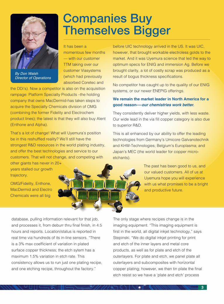
It has been a momentous few months --- with our customer TTM taking over our customer Viasystems (which had previously absorbed Coretec and
the DDi’s). Now a competitor is also on the acquisition rampage: Platform Specialty Products –the holding company that owns MacDermid-has taken steps to acquire the Specialty Chemicals division of OMG (combining the former Fidelity and Electrochem product lines); the latest is that they will also buy Alent (Enthone and Alpha).
That’s a lot of change! What will Uyemura’s position be in this reshuffled reality? We’ll still have the strongest R&D resources in the world plating industry, and offer the best technologies and service to our customers. That will not change, and competing with other giants has never in 20+ years stalled our growth trajectory.
OMG/Fidelity, Enthone, MacDermid and Electro Chemicals were all big
Companies BuyThemselves Bigger
before UIC technology arrived in the US. It was UIC, however, that brought workable electroless golds to the market. And it was Uyemura science that led the way to optimum specs for ENIG and immersion Ag. Before we brought clarity, a lot of costly scrap was produced as a result of bogus thickness specifications.
No competitor has caught up to the quality of our ENIG systems, or our newer ENEPIG offerings.
We remain the market leader in North America for a good reason----our chemistries work better.
They consistently deliver higher yields, with less waste. Our wide lead in the via fill copper category is also due to superior R&D.
This is all enhanced by our ability to offer the leading technologies from Germany’s Umicore Galvanotechnik and KHW-Technologies; Belgium’s Europlasma; and Japan’s MEC (the world leader for copper micro-etchants).
The past has been good to us, and our valued customers. All of us at Uyemura hope you will experience with us what promises to be a bright and productive future.
“We also wanted an ROI of no more than 5 years, and although the industry minimum average headcount for a facility of this scale is 100 workers, we wanted to achieve everything with a workforce of no more than 17 total employees.”
Stepinski completed his initial design/business plan in 6 weeks: a unique U-shaped configuration 550’ long, with a 4.5 hour cycle time on a 50,000 sq-ft overall footprint.
A 2-level command center is elevated 12’ above the line. The first level is a chem lab, where one technician does wet process and cross-sectional analysis testing for the entire facility, in 6 hours per day. Both levels also house banks of monitors that track the temperature, concentration and level of every chemical, and the progress of each order. The line uses 39 pieces of automation linking 24 value-added process steps.
“We are really focused on lean concepts of waste reduction,” Stepinski continues. “Chemistry is stored in vented day tanks, with sensors monitoring levels and checking for leaks. Live inventory data is
database, pulling information relevant for that job, and processes it, from deburr thru final finish, in 4.5 hours and reports. Location/status is reported in real time via hundreds of its in-line sensors. “There is a 3% max coefficient of variation in plated surface copper thickness; the etch sytem has a maximum 1.5% variation in etch rate. This consistency allows us to run just one plating recipe, and one etching recipe, throughout the factory.”
The only stage where recipes change is in the imaging equipment. “This imaging equipment is first in the world, all digital inkjet technology,” says Stepinski. “We do digital inkjet printing for print and etch of the inner layers and metal core products, as well as for plate and etch of the outerlayers. For plate and etch, we panel plate all outerlayers and subcomposites with horizontal copper plating; however, we then tin plate the final etch resist so we have a ‘plate and etch’ process
with an inkjet resist.” Soldermask and legend processes are also inkjet. “This eliminates costly steps in photolithography: we don’t have a laminator or developer for primary imaging, nor a cleaner, microetch, or pre-dip for etch resist electro-plating.
“Additonally, our tin plater is so robust, we can afford to plate only 2.2-2.9 microns of tin on the surface.”
Due to this low thickness, 2 spray bars at 1.5 meters per minute are all that is needed to strip the tin after etching. “We only use a drum of standard tin strip chemistry every 16,000 panels, and a drum of tin brightener every 42,000 panels. A drum of resist stripper lasts for 14,000 panels with our wax-based inkjet ink.”
The most difficult process to integrate in the line was the imaging technology, which is markedly different from what’s been done previously. “We had to work with our suppliers and take it from an idea to a production process in a very short time.” The
A thorough analysis of current product designs and roadmap tolerance requirements was used to establish process spec targets.
“Extensive experimentation with large quantities of test panels was also required to adjust the plating thickness variation to the required level across our entire product mix. But by designing it all up-front, and systematically qualifying it, we now have a robust, predictable, low maintenance process for many years to come.”
Process controls were qualified to the point that no test panels are needed to interrupt production to qualify different product recipes, nor are any dummy panels required to compensate for current density edge effects. Whelen’s metallization process is “green” and based upon conductive polymer.
Q: You are known for your expertise with ENIG. How would you differentiate the Uyemura product from others in the market?
A. The process cost for nickel plating can be as
much as twice as high when dummy plating is
required after downtime or to meet minimum
loading requirements. Deactivation of most
nickel baths can occur in less than 2 hours. At
this point, dummy plating becomes necessary,
which increases costs dramatically by using
much more chemistry and labor.
Dummy plating has effectively been made obsolete
with UIC’s ENIG. The UIC process, in fact, does not
'deactivate' at all. The first basket of panels
processed after many hours or even a full day, can
be live production parts.
The second differentiator involves minimum load
factor. Whether you're running gold afterwards, or
ENEPIG, you can run one 3" X 4” coupon or a full
basket of 18" X 24" panels in (UIC’s) NPR-4
electroless nickel, and the Ni plated thickness will be
identical. When users of competitors‘ chemistry
have a small area 'hot job,' more square footage of
work is required per gallon of solution for the bath to
perform properly.
Control of the bath is also key. Uyemura Japan and
Uyemura USA have a controller (STARLiNE-DASH®
4-NP) that is phenomenal. The DASH 4-NP samples
the EN plating solution, cools it, analyzes all the
components, including pH values, and replenishes
automatically. As a result, baths can be maintained
continuously at 2-4% of optimum; nickel can be
controlled within +/-0.05 g/L.
Q. What about the issue of turnovers?
A. As nickel baths age from 0 to 5 metal turnovers, the
plating rate slows down. Virtually everyone dumps
the bath at 5 MTO, or does a transfer-nitric clean-
ing-return procedure. The problem with competitors’
baths is as the nickel plating rate goes down,
additional process changes are required to
compensate for it. Our controller compensates for
metal turnovers and adjusts the components
automatically. So, at 1, or 3 - or 5 MTOs, there's zero
difference in plated results.
Finally, the UIC nickel bath gets points for stability.
Five months in, look in the tank and see how much
nickel plated out in any competitor’s bath. With
ours, the amount is substantially less. Plate-out is
a huge waste of material, and the nitric stripping
required to eliminate it produces hazardous waste.
The bottom line with ENIG is you want gold
deposition with perfect uniformity. We control the
phosphorus content in the nickel bath at 6-8% so
that gold distribution is exactly that: perfectly
uniform. Standards are met, and there are no
outliers - no isolated pads that needlessly get
more gold.
Two of the largest circuit board manufacturers in
North America – independent of each other -
compared 5 ENIG suppliers for corrosion and gold
distribution. UIC’s was first for gold uniformity on
isolated features, and for lowest corrosion.
The system was designed so there’s no need to vent ammonia etch. “By performing the oxidation reaction offline in a separate sealed reactor, we’ve created a totally closed system.” Rinses are regenerated with a proprietary process as well. Virtually no hazwaste is generated (overall hazwaste volume as a stand-alone PCB shop meets the conditions of a small quantity generator, the company is regulated at a higher level).
Whelen was able to ‘design-out’ pollution concerns because the factory and waste treatment were a single, integrated design. “Our operating costs for waste treatment are far below conventional systems, and even our capital investment in waste treatment was below average for a shop our size” says Stepinski.
“There are practically no treatment chemicals used, except for minute amounts of acid and caustic. The high level of recycling that we do actually offsets most of the operating costs of our environmental systems. On a per-panel basis, conventional factories spend more money on fresh water than we spend on all of our combined regulatory operations.”
The manufacturing model developed for PCBs by Whelen Engineering is a Proof of Concept that’s applicable, in the company’s view, for many products. “The key,” says Stepinski, “is not just automation of a single piece of equipment, (in operations like drilling, plating, imaging, etc.), but
the combining of new technologies, such as inkjet and others, and the use of new, more efficient, more integrated process equipment.”
The Whelen model is a new solution that addresses this competitive advantage by engineering the integration of different processes to a new level of efficiency according to Stepinski. “The majority of the cost of quality in manufacturing boards is non-valued waste stemming from a lack of inter-process integration. This can be up to 80-90%
of a typical shop’s labor costs, and essentially all of the regulatory costs.”
Whelen’s market share is 80% in the US; the company is also very strong in South America, Europe and the Middle East. “This is a smart, private company that takes the long view. As a result, it is
loop recycling system for ammonia etchant.” It covers every waste aspect of the system. “We plate the copper out of the etchant, and rather than ammonium chloride for etching, we use a cocktail of ammonium sulfate and other low cost generic compunds, which we developed in partnership with a supplier to plate out the copper.
“We sell the 99.9% pure copper to a local recycler, and do not add any fresh chemicals to the etcher (chemicals were only needed for initial makeup). Our plating chemistry supplier has even approved the copper quality from the etcher for reuse in the plater, which will allow us to take copper that is removed at etch to be redissolved in the plater.
“This reduced our overall raw copper purchases by 95%, and allowed us to metallize the circuit pattern using waste copper from the laminate.”
continuously available. Tanks are sized for 3X supply chain average lead time. Our day tank system also reduces the number of manual chemical transactions by 99% versus a conven-tional facility by eliminating the hazardous, labor-intensive manual adds from the partially used drums. All adds are made via an HMI interface controlling metering pumps with safety interlocks. Laminate, masks and other solid materials are also stored in highly visible locations, with no central inventory.”
At the start of production, drilled panels are placed in a tray, which is barcoded; the tray then pings the
“Everyone who comes through this plant sees it as the next step in the evolution of making PCBs,” he adds, “and a solid ‘Proof of Concept’ for efficiently making many other products as well.”
At the time, Whelen Engineering was spending millions of dollars each year on PCBs from China; prices and lead times were both on an upward trajectory. Injection molding and other critical operations had already been brought in-house, with results exceeding forecasts. A strategic decision was made to explore whether board making could be next.
In Spring 2013, management recruited Alex Stepinski, whose experience included senior engineering and management roles at large North American PCB Fab companies to develop a plan. He was, in his words, “all about nonconventional approaches.”
“The idea,” explains Stepinski, “was to build a fully
automated operation based on our core principles
that would produce a higher quality PWB, at a lower
price, with shorter lead times than offshore. The takt requirement to achieve 100% reshoring was PC board output of 50 panels per hour; translating to 2500 per week of 18” X 24” and 21” X 24”, rigid and rigid-flex panels; with capacity to expand up to 10,000 panels per week over the next decade.
able to make substantial multi-year investments without having to defend itself against shareholders hungry for the next quarterly guidance.”
3
The production ramp is underway and expected to be completed shortly whereupon, Whelen Engi-neering will have 100% of its PCB production back in the USA – and bragging rights about achieving substantial cost savings over PCBs from China. “That includes both direct and indirect costs, as well as massive savings in cycle time,” says Stepinski. “We expect to be the first shop in the west to out-compete the Asia-Pacific region on direct PCB price per square inch.”
It is also the first totally “green” pcb shop. Explains Stepinski, “there is no need for wastewater permits, or air permits; liquid is 100% recycled, and we designed-out all of the air toxics.” A non-regulated resist stripper was developed as well. “We use just 500 gallons of fresh water a day to compensate for humidity loss from our air scrubber (which runs on recycled DI water to maximize absorption efficiency), and we have the first in the world, closed
imaging integration has, however, produced the most profound benefit in terms of labor savings. In addition, one worker manages the copper plate, metallization, tin plater, etch, resist, and tin stripping operations. “Our solder mask inkjet-based process is the only one in the world which also plugs the boards simultaneously with coating.”
China and Korea are today’s LCC (Low Cost Country) manufacturers for PC boards of all types.
In 2012, Whelen Engineering (Chester, CT and Charlestown, NH) was among the tens of thousands of OEMs that sourced their PCBs from Asia. Then, a perfect storm of intellectual property issues, lengthening lead times and increasing cost led the company to build - greenfield and-in-house – America’s first new rigid PCB shop in 15 years.
Whelen Engineering is a leading manufacturer of safety lighting and sirens for automotive, aviation and emergency warning applications. Their about-face in how they source the brains for every product they sell tells an important story about the power of innovation, the merits of questioning common wisdom, and how both of these can generate a Proof of Concept with implications far beyond one manufacturing operation.
Whelen was founded (in 1952) on the pillars of advanced production equipment, a motivated
workforce, and a commitment to vertical manufac-turing initiatives. In 2012, the company’s visionary CEO, John Olson, launched a new project that would take that vertical integration to an entirely new level.
20KV X350 50µM 47 30 SEI
“We also wanted an ROI of no more than 5 years, and although the industry minimum average headcount for a facility of this scale is 100 workers, we wanted to achieve everything with a workforce of no more than 17 total employees.”
Stepinski completed his initial design/business plan in 6 weeks: a unique U-shaped configuration 550’ long, with a 4.5 hour cycle time on a 50,000 sq-ft overall footprint.
A 2-level command center is elevated 12’ above the line. The first level is a chem lab, where one technician does wet process and cross-sectional analysis testing for the entire facility, in 6 hours per day. Both levels also house banks of monitors that track the temperature, concentration and level of every chemical, and the progress of each order. The line uses 39 pieces of automation linking 24 value-added process steps.
“We are really focused on lean concepts of waste reduction,” Stepinski continues. “Chemistry is stored in vented day tanks, with sensors monitoring levels and checking for leaks. Live inventory data is
database, pulling information relevant for that job, and processes it, from deburr thru final finish, in 4.5 hours and reports. Location/status is reported in real time via hundreds of its in-line sensors. “There is a 3% max coefficient of variation in plated surface copper thickness; the etch sytem has a maximum 1.5% variation in etch rate. This consistency allows us to run just one plating recipe, and one etching recipe, throughout the factory.”
The only stage where recipes change is in the imaging equipment. “This imaging equipment is first in the world, all digital inkjet technology,” says Stepinski. “We do digital inkjet printing for print and etch of the inner layers and metal core products, as well as for plate and etch of the outerlayers. For plate and etch, we panel plate all outerlayers and subcomposites with horizontal copper plating; however, we then tin plate the final etch resist so we have a ‘plate and etch’ process
with an inkjet resist.” Soldermask and legend processes are also inkjet. “This eliminates costly steps in photolithography: we don’t have a laminator or developer for primary imaging, nor a cleaner, microetch, or pre-dip for etch resist electro-plating.
“Additonally, our tin plater is so robust, we can afford to plate only 2.2-2.9 microns of tin on the surface.”
Due to this low thickness, 2 spray bars at 1.5 meters per minute are all that is needed to strip the tin after etching. “We only use a drum of standard tin strip chemistry every 16,000 panels, and a drum of tin brightener every 42,000 panels. A drum of resist stripper lasts for 14,000 panels with our wax-based inkjet ink.”
The most difficult process to integrate in the line was the imaging technology, which is markedly different from what’s been done previously. “We had to work with our suppliers and take it from an idea to a production process in a very short time.” The
A thorough analysis of current product designs and roadmap tolerance requirements was used to establish process spec targets.
“Extensive experimentation with large quantities of test panels was also required to adjust the plating thickness variation to the required level across our entire product mix. But by designing it all up-front, and systematically qualifying it, we now have a robust, predictable, low maintenance process for many years to come.”
Process controls were qualified to the point that no test panels are needed to interrupt production to qualify different product recipes, nor are any dummy panels required to compensate for current density edge effects. Whelen’s metallization process is “green” and based upon conductive polymer.
Q: You are known for your expertise with ENIG. How would you differentiate the Uyemura product from others in the market?
A. The process cost for nickel plating can be as
much as twice as high when dummy plating is
required after downtime or to meet minimum
loading requirements. Deactivation of most
nickel baths can occur in less than 2 hours. At
this point, dummy plating becomes necessary,
which increases costs dramatically by using
much more chemistry and labor.
Dummy plating has effectively been made obsolete
with UIC’s ENIG. The UIC process, in fact, does not
'deactivate' at all. The first basket of panels
processed after many hours or even a full day, can
be live production parts.
The second differentiator involves minimum load
factor. Whether you're running gold afterwards, or
ENEPIG, you can run one 3" X 4” coupon or a full
basket of 18" X 24" panels in (UIC’s) NPR-4
electroless nickel, and the Ni plated thickness will be
identical. When users of competitors‘ chemistry
have a small area 'hot job,' more square footage of
work is required per gallon of solution for the bath to
perform properly.
Control of the bath is also key. Uyemura Japan and
Uyemura USA have a controller (STARLiNE-DASH®
4-NP) that is phenomenal. The DASH 4-NP samples
the EN plating solution, cools it, analyzes all the
components, including pH values, and replenishes
automatically. As a result, baths can be maintained
continuously at 2-4% of optimum; nickel can be
controlled within +/-0.05 g/L.
Q. What about the issue of turnovers?
A. As nickel baths age from 0 to 5 metal turnovers, the
plating rate slows down. Virtually everyone dumps
the bath at 5 MTO, or does a transfer-nitric clean-
ing-return procedure. The problem with competitors’
baths is as the nickel plating rate goes down,
additional process changes are required to
compensate for it. Our controller compensates for
metal turnovers and adjusts the components
automatically. So, at 1, or 3 - or 5 MTOs, there's zero
difference in plated results.
Finally, the UIC nickel bath gets points for stability.
Five months in, look in the tank and see how much
nickel plated out in any competitor’s bath. With
ours, the amount is substantially less. Plate-out is
a huge waste of material, and the nitric stripping
required to eliminate it produces hazardous waste.
The bottom line with ENIG is you want gold
deposition with perfect uniformity. We control the
phosphorus content in the nickel bath at 6-8% so
that gold distribution is exactly that: perfectly
uniform. Standards are met, and there are no
outliers - no isolated pads that needlessly get
more gold.
Two of the largest circuit board manufacturers in
North America – independent of each other -
compared 5 ENIG suppliers for corrosion and gold
distribution. UIC’s was first for gold uniformity on
isolated features, and for lowest corrosion.
The system was designed so there’s no need to vent ammonia etch. “By performing the oxidation reaction offline in a separate sealed reactor, we’ve created a totally closed system.” Rinses are regenerated with a proprietary process as well. Virtually no hazwaste is generated (overall hazwaste volume as a stand-alone PCB shop meets the conditions of a small quantity generator, the company is regulated at a higher level).
Whelen was able to ‘design-out’ pollution concerns because the factory and waste treatment were a single, integrated design. “Our operating costs for waste treatment are far below conventional systems, and even our capital investment in waste treatment was below average for a shop our size” says Stepinski.
“There are practically no treatment chemicals used, except for minute amounts of acid and caustic. The high level of recycling that we do actually offsets most of the operating costs of our environmental systems. On a per-panel basis, conventional factories spend more money on fresh water than we spend on all of our combined regulatory operations.”
The manufacturing model developed for PCBs by Whelen Engineering is a Proof of Concept that’s applicable, in the company’s view, for many products. “The key,” says Stepinski, “is not just automation of a single piece of equipment, (in operations like drilling, plating, imaging, etc.), but
the combining of new technologies, such as inkjet and others, and the use of new, more efficient, more integrated process equipment.”
The Whelen model is a new solution that addresses this competitive advantage by engineering the integration of different processes to a new level of efficiency according to Stepinski. “The majority of the cost of quality in manufacturing boards is non-valued waste stemming from a lack of inter-process integration. This can be up to 80-90%
Panel ready for solder and final finish
of a typical shop’s labor costs, and essentially all of the regulatory costs.”
Whelen’s market share is 80% in the US; the company is also very strong in South America, Europe and the Middle East. “This is a smart, private company that takes the long view. As a result, it is
loop recycling system for ammonia etchant.” It covers every waste aspect of the system. “We plate the copper out of the etchant, and rather than ammonium chloride for etching, we use a cocktail of ammonium sulfate and other low cost generic compunds, which we developed in partnership with a supplier to plate out the copper.
“We sell the 99.9% pure copper to a local recycler, and do not add any fresh chemicals to the etcher (chemicals were only needed for initial makeup). Our plating chemistry supplier has even approved the copper quality from the etcher for reuse in the plater, which will allow us to take copper that is removed at etch to be redissolved in the plater.
“This reduced our overall raw copper purchases by 95%, and allowed us to metallize the circuit pattern using waste copper from the laminate.”
continuously available. Tanks are sized for 3X supply chain average lead time. Our day tank system also reduces the number of manual chemical transactions by 99% versus a conven-tional facility by eliminating the hazardous, labor-intensive manual adds from the partially used drums. All adds are made via an HMI interface controlling metering pumps with safety interlocks. Laminate, masks and other solid materials are also stored in highly visible locations, with no central inventory.”
At the start of production, drilled panels are placed in a tray, which is barcoded; the tray then pings the
“Everyone who comes through this plant sees it as the next step in the evolution of making PCBs,” he adds, “and a solid ‘Proof of Concept’ for efficiently making many other products as well.”
At the time, Whelen Engineering was spending millions of dollars each year on PCBs from China; prices and lead times were both on an upward trajectory. Injection molding and other critical operations had already been brought in-house, with results exceeding forecasts. A strategic decision was made to explore whether board making could be next.
In Spring 2013, management recruited Alex Stepinski, whose experience included senior engineering and management roles at large North American PCB Fab companies to develop a plan. He was, in his words, “all about nonconventional approaches.”
“The idea,” explains Stepinski, “was to build a fully
automated operation based on our core principles
that would produce a higher quality PWB, at a lower
price, with shorter lead times than offshore. The takt requirement to achieve 100% reshoring was PC board output of 50 panels per hour; translating to 2500 per week of 18” X 24” and 21” X 24”, rigid and rigid-flex panels; with capacity to expand up to 10,000 panels per week over the next decade.
able to make substantial multi-year investments without having to defend itself against shareholders hungry for the next quarterly guidance.”
4
Whelen Engineeringuses Uyemura ENIG,the industry standardfor mid-phos EN with immersion gold.

The production ramp is underway and expected to be completed shortly whereupon, Whelen Engi-neering will have 100% of its PCB production back in the USA – and bragging rights about achieving substantial cost savings over PCBs from China. “That includes both direct and indirect costs, as well as massive savings in cycle time,” says Stepinski. “We expect to be the first shop in the west to out-compete the Asia-Pacific region on direct PCB price per square inch.”
It is also the first totally “green” pcb shop. Explains Stepinski, “there is no need for wastewater permits, or air permits; liquid is 100% recycled, and we designed-out all of the air toxics.” A non-regulated resist stripper was developed as well. “We use just 500 gallons of fresh water a day to compensate for humidity loss from our air scrubber (which runs on recycled DI water to maximize absorption efficiency), and we have the first in the world, closed
imaging integration has, however, produced the most profound benefit in terms of labor savings. In addition, one worker manages the copper plate, metallization, tin plater, etch, resist, and tin stripping operations. “Our solder mask inkjet-based process is the only one in the world which also plugs the boards simultaneously with coating.”
China and Korea are today’s LCC (Low Cost Country) manufacturers for PC boards of all types.
In 2012, Whelen Engineering (Chester, CT and Charlestown, NH) was among the tens of thousands of OEMs that sourced their PCBs from Asia. Then, a perfect storm of intellectual property issues, lengthening lead times and increasing cost led the company to build - greenfield and-in-house – America’s first new rigid PCB shop in 15 years.
Whelen Engineering is a leading manufacturer of safety lighting and sirens for automotive, aviation and emergency warning applications. Their about-face in how they source the brains for every product they sell tells an important story about the power of innovation, the merits of questioning common wisdom, and how both of these can generate a Proof of Concept with implications far beyond one manufacturing operation.
Whelen was founded (in 1952) on the pillars of advanced production equipment, a motivated
workforce, and a commitment to vertical manufac-turing initiatives. In 2012, the company’s visionary CEO, John Olson, launched a new project that would take that vertical integration to an entirely new level.
“We also wanted an ROI of no more than 5 years, and although the industry minimum average headcount for a facility of this scale is 100 workers, we wanted to achieve everything with a workforce of no more than 17 total employees.”
Stepinski completed his initial design/business plan in 6 weeks: a unique U-shaped configuration 550’ long, with a 4.5 hour cycle time on a 50,000 sq-ft overall footprint.
A 2-level command center is elevated 12’ above the line. The first level is a chem lab, where one technician does wet process and cross-sectional analysis testing for the entire facility, in 6 hours per day. Both levels also house banks of monitors that track the temperature, concentration and level of every chemical, and the progress of each order. The line uses 39 pieces of automation linking 24 value-added process steps.
“We are really focused on lean concepts of waste reduction,” Stepinski continues. “Chemistry is stored in vented day tanks, with sensors monitoring levels and checking for leaks. Live inventory data is
database, pulling information relevant for that job, and processes it, from deburr thru final finish, in 4.5 hours and reports. Location/status is reported in real time via hundreds of its in-line sensors. “There is a 3% max coefficient of variation in plated surface copper thickness; the etch sytem has a maximum 1.5% variation in etch rate. This consistency allows us to run just one plating recipe, and one etching recipe, throughout the factory.”
The only stage where recipes change is in the imaging equipment. “This imaging equipment is first in the world, all digital inkjet technology,” says Stepinski. “We do digital inkjet printing for print and etch of the inner layers and metal core products, as well as for plate and etch of the outerlayers. For plate and etch, we panel plate all outerlayers and subcomposites with horizontal copper plating; however, we then tin plate the final etch resist so we have a ‘plate and etch’ process
with an inkjet resist.” Soldermask and legend processes are also inkjet. “This eliminates costly steps in photolithography: we don’t have a laminator or developer for primary imaging, nor a cleaner, microetch, or pre-dip for etch resist electro-plating.
“Additonally, our tin plater is so robust, we can afford to plate only 2.2-2.9 microns of tin on the surface.”
Due to this low thickness, 2 spray bars at 1.5 meters per minute are all that is needed to strip the tin after etching. “We only use a drum of standard tin strip chemistry every 16,000 panels, and a drum of tin brightener every 42,000 panels. A drum of resist stripper lasts for 14,000 panels with our wax-based inkjet ink.”
The most difficult process to integrate in the line was the imaging technology, which is markedly different from what’s been done previously. “We had to work with our suppliers and take it from an idea to a production process in a very short time.” The
A thorough analysis of current product designs and roadmap tolerance requirements was used to establish process spec targets.
“Extensive experimentation with large quantities of test panels was also required to adjust the plating thickness variation to the required level across our entire product mix. But by designing it all up-front, and systematically qualifying it, we now have a robust, predictable, low maintenance process for many years to come.”
Process controls were qualified to the point that no test panels are needed to interrupt production to qualify different product recipes, nor are any dummy panels required to compensate for current density edge effects. Whelen’s metallization process is “green” and based upon conductive polymer.
Q: You are known for your expertise with ENIG. How would you differentiate the Uyemura product from others in the market?
A. The process cost for nickel plating can be as
much as twice as high when dummy plating is
required after downtime or to meet minimum
loading requirements. Deactivation of most
nickel baths can occur in less than 2 hours. At
this point, dummy plating becomes necessary,
which increases costs dramatically by using
much more chemistry and labor.
Dummy plating has effectively been made obsolete
with UIC’s ENIG. The UIC process, in fact, does not
'deactivate' at all. The first basket of panels
processed after many hours or even a full day, can
be live production parts.
The second differentiator involves minimum load
factor. Whether you're running gold afterwards, or
ENEPIG, you can run one 3" X 4” coupon or a full
basket of 18" X 24" panels in (UIC’s) NPR-4
electroless nickel, and the Ni plated thickness will be
identical. When users of competitors‘ chemistry
have a small area 'hot job,' more square footage of
work is required per gallon of solution for the bath to
perform properly.
Control of the bath is also key. Uyemura Japan and
Uyemura USA have a controller (STARLiNE-DASH®
4-NP) that is phenomenal. The DASH 4-NP samples
the EN plating solution, cools it, analyzes all the
components, including pH values, and replenishes
automatically. As a result, baths can be maintained
continuously at 2-4% of optimum; nickel can be
controlled within +/-0.05 g/L.
Q. What about the issue of turnovers?
A. As nickel baths age from 0 to 5 metal turnovers, the
plating rate slows down. Virtually everyone dumps
the bath at 5 MTO, or does a transfer-nitric clean-
ing-return procedure. The problem with competitors’
baths is as the nickel plating rate goes down,
additional process changes are required to
compensate for it. Our controller compensates for
metal turnovers and adjusts the components
automatically. So, at 1, or 3 - or 5 MTOs, there's zero
difference in plated results.
Finally, the UIC nickel bath gets points for stability.
Five months in, look in the tank and see how much
nickel plated out in any competitor’s bath. With
ours, the amount is substantially less. Plate-out is
a huge waste of material, and the nitric stripping
required to eliminate it produces hazardous waste.
The bottom line with ENIG is you want gold
deposition with perfect uniformity. We control the
phosphorus content in the nickel bath at 6-8% so
that gold distribution is exactly that: perfectly
uniform. Standards are met, and there are no
outliers - no isolated pads that needlessly get
more gold.
Two of the largest circuit board manufacturers in
North America – independent of each other -
compared 5 ENIG suppliers for corrosion and gold
distribution. UIC’s was first for gold uniformity on
isolated features, and for lowest corrosion.
The system was designed so there’s no need to vent ammonia etch. “By performing the oxidation reaction offline in a separate sealed reactor, we’ve created a totally closed system.” Rinses are regenerated with a proprietary process as well. Virtually no hazwaste is generated (overall hazwaste volume as a stand-alone PCB shop meets the conditions of a small quantity generator, the company is regulated at a higher level).
Whelen was able to ‘design-out’ pollution concerns because the factory and waste treatment were a single, integrated design. “Our operating costs for waste treatment are far below conventional systems, and even our capital investment in waste treatment was below average for a shop our size” says Stepinski.
“There are practically no treatment chemicals used, except for minute amounts of acid and caustic. The high level of recycling that we do actually offsets most of the operating costs of our environmental systems. On a per-panel basis, conventional factories spend more money on fresh water than we spend on all of our combined regulatory operations.”
The manufacturing model developed for PCBs by Whelen Engineering is a Proof of Concept that’s applicable, in the company’s view, for many products. “The key,” says Stepinski, “is not just automation of a single piece of equipment, (in operations like drilling, plating, imaging, etc.), but
the combining of new technologies, such as inkjet and others, and the use of new, more efficient, more integrated process equipment.”
The Whelen model is a new solution that addresses this competitive advantage by engineering the integration of different processes to a new level of efficiency according to Stepinski. “The majority of the cost of quality in manufacturing boards is non-valued waste stemming from a lack of inter-process integration. This can be up to 80-90%
In-line horizontal electroplated copper
of a typical shop’s labor costs, and essentially all of the regulatory costs.”
Whelen’s market share is 80% in the US; the company is also very strong in South America, Europe and the Middle East. “This is a smart, private company that takes the long view. As a result, it is
loop recycling system for ammonia etchant.” It covers every waste aspect of the system. “We plate the copper out of the etchant, and rather than ammonium chloride for etching, we use a cocktail of ammonium sulfate and other low cost generic compunds, which we developed in partnership with a supplier to plate out the copper.
“We sell the 99.9% pure copper to a local recycler, and do not add any fresh chemicals to the etcher (chemicals were only needed for initial makeup). Our plating chemistry supplier has even approved the copper quality from the etcher for reuse in the plater, which will allow us to take copper that is removed at etch to be redissolved in the plater.
“This reduced our overall raw copper purchases by 95%, and allowed us to metallize the circuit pattern using waste copper from the laminate.”
continuously available. Tanks are sized for 3X supply chain average lead time. Our day tank system also reduces the number of manual chemical transactions by 99% versus a conven-tional facility by eliminating the hazardous, labor-intensive manual adds from the partially used drums. All adds are made via an HMI interface controlling metering pumps with safety interlocks. Laminate, masks and other solid materials are also stored in highly visible locations, with no central inventory.”
At the start of production, drilled panels are placed in a tray, which is barcoded; the tray then pings the
“Everyone who comes through this plant sees it as the next step in the evolution of making PCBs,” he adds, “and a solid ‘Proof of Concept’ for efficiently making many other products as well.”
At the time, Whelen Engineering was spending millions of dollars each year on PCBs from China; prices and lead times were both on an upward trajectory. Injection molding and other critical operations had already been brought in-house, with results exceeding forecasts. A strategic decision was made to explore whether board making could be next.
In Spring 2013, management recruited Alex Stepinski, whose experience included senior engineering and management roles at large North American PCB Fab companies to develop a plan. He was, in his words, “all about nonconventional approaches.”
“The idea,” explains Stepinski, “was to build a fully
automated operation based on our core principles
that would produce a higher quality PWB, at a lower
price, with shorter lead times than offshore. The takt requirement to achieve 100% reshoring was PC board output of 50 panels per hour; translating to 2500 per week of 18” X 24” and 21” X 24”, rigid and rigid-flex panels; with capacity to expand up to 10,000 panels per week over the next decade.
able to make substantial multi-year investments without having to defend itself against shareholders hungry for the next quarterly guidance.”
We expect to be the first shop in the west to out-compete the Asia-Pacific region on direct PCB price per square inch.
We expect to be the first shop in the west to out-compete the Asia-Pacific region on direct PCB price per square inch.
5

The production ramp is underway and expected to be completed shortly whereupon, Whelen Engi-neering will have 100% of its PCB production back in the USA – and bragging rights about achieving substantial cost savings over PCBs from China. “That includes both direct and indirect costs, as well as massive savings in cycle time,” says Stepinski. “We expect to be the first shop in the west to out-compete the Asia-Pacific region on direct PCB price per square inch.”
It is also the first totally “green” pcb shop. Explains Stepinski, “there is no need for wastewater permits, or air permits; liquid is 100% recycled, and we designed-out all of the air toxics.” A non-regulated resist stripper was developed as well. “We use just 500 gallons of fresh water a day to compensate for humidity loss from our air scrubber (which runs on recycled DI water to maximize absorption efficiency), and we have the first in the world, closed
imaging integration has, however, produced the most profound benefit in terms of labor savings. In addition, one worker manages the copper plate, metallization, tin plater, etch, resist, and tin stripping operations. “Our solder mask inkjet-based process is the only one in the world which also plugs the boards simultaneously with coating.”
China and Korea are today’s LCC (Low Cost Country) manufacturers for PC boards of all types.
In 2012, Whelen Engineering (Chester, CT and Charlestown, NH) was among the tens of thousands of OEMs that sourced their PCBs from Asia. Then, a perfect storm of intellectual property issues, lengthening lead times and increasing cost led the company to build - greenfield and-in-house – America’s first new rigid PCB shop in 15 years.
Whelen Engineering is a leading manufacturer of safety lighting and sirens for automotive, aviation and emergency warning applications. Their about-face in how they source the brains for every product they sell tells an important story about the power of innovation, the merits of questioning common wisdom, and how both of these can generate a Proof of Concept with implications far beyond one manufacturing operation.
Whelen was founded (in 1952) on the pillars of advanced production equipment, a motivated
workforce, and a commitment to vertical manufac-turing initiatives. In 2012, the company’s visionary CEO, John Olson, launched a new project that would take that vertical integration to an entirely new level.
“We also wanted an ROI of no more than 5 years, and although the industry minimum average headcount for a facility of this scale is 100 workers, we wanted to achieve everything with a workforce of no more than 17 total employees.”
Stepinski completed his initial design/business plan in 6 weeks: a unique U-shaped configuration 550’ long, with a 4.5 hour cycle time on a 50,000 sq-ft overall footprint.
A 2-level command center is elevated 12’ above the line. The first level is a chem lab, where one technician does wet process and cross-sectional analysis testing for the entire facility, in 6 hours per day. Both levels also house banks of monitors that track the temperature, concentration and level of every chemical, and the progress of each order. The line uses 39 pieces of automation linking 24 value-added process steps.
“We are really focused on lean concepts of waste reduction,” Stepinski continues. “Chemistry is stored in vented day tanks, with sensors monitoring levels and checking for leaks. Live inventory data is
database, pulling information relevant for that job, and processes it, from deburr thru final finish, in 4.5 hours and reports. Location/status is reported in real time via hundreds of its in-line sensors. “There is a 3% max coefficient of variation in plated surface copper thickness; the etch sytem has a maximum 1.5% variation in etch rate. This consistency allows us to run just one plating recipe, and one etching recipe, throughout the factory.”
The only stage where recipes change is in the imaging equipment. “This imaging equipment is first in the world, all digital inkjet technology,” says Stepinski. “We do digital inkjet printing for print and etch of the inner layers and metal core products, as well as for plate and etch of the outerlayers. For plate and etch, we panel plate all outerlayers and subcomposites with horizontal copper plating; however, we then tin plate the final etch resist so we have a ‘plate and etch’ process
with an inkjet resist.” Soldermask and legend processes are also inkjet. “This eliminates costly steps in photolithography: we don’t have a laminator or developer for primary imaging, nor a cleaner, microetch, or pre-dip for etch resist electro-plating.
“Additonally, our tin plater is so robust, we can afford to plate only 2.2-2.9 microns of tin on the surface.”
Due to this low thickness, 2 spray bars at 1.5 meters per minute are all that is needed to strip the tin after etching. “We only use a drum of standard tin strip chemistry every 16,000 panels, and a drum of tin brightener every 42,000 panels. A drum of resist stripper lasts for 14,000 panels with our wax-based inkjet ink.”
The most difficult process to integrate in the line was the imaging technology, which is markedly different from what’s been done previously. “We had to work with our suppliers and take it from an idea to a production process in a very short time.” The
A thorough analysis of current product designs and roadmap tolerance requirements was used to establish process spec targets.
“Extensive experimentation with large quantities of test panels was also required to adjust the plating thickness variation to the required level across our entire product mix. But by designing it all up-front, and systematically qualifying it, we now have a robust, predictable, low maintenance process for many years to come.”
Process controls were qualified to the point that no test panels are needed to interrupt production to qualify different product recipes, nor are any dummy panels required to compensate for current density edge effects. Whelen’s metallization process is “green” and based upon conductive polymer.
Q: You are known for your expertise with ENIG. How would you differentiate the Uyemura product from others in the market?
A. The process cost for nickel plating can be as
much as twice as high when dummy plating is
required after downtime or to meet minimum
loading requirements. Deactivation of most
nickel baths can occur in less than 2 hours. At
this point, dummy plating becomes necessary,
which increases costs dramatically by using
much more chemistry and labor.
Dummy plating has effectively been made obsolete
with UIC’s ENIG. The UIC process, in fact, does not
'deactivate' at all. The first basket of panels
processed after many hours or even a full day, can
be live production parts.
The second differentiator involves minimum load
factor. Whether you're running gold afterwards, or
ENEPIG, you can run one 3" X 4” coupon or a full
basket of 18" X 24" panels in (UIC’s) NPR-4
electroless nickel, and the Ni plated thickness will be
identical. When users of competitors‘ chemistry
have a small area 'hot job,' more square footage of
work is required per gallon of solution for the bath to
perform properly.
Control of the bath is also key. Uyemura Japan and
Uyemura USA have a controller (STARLiNE-DASH®
4-NP) that is phenomenal. The DASH 4-NP samples
the EN plating solution, cools it, analyzes all the
components, including pH values, and replenishes
automatically. As a result, baths can be maintained
continuously at 2-4% of optimum; nickel can be
controlled within +/-0.05 g/L.
Q. What about the issue of turnovers?
A. As nickel baths age from 0 to 5 metal turnovers, the
plating rate slows down. Virtually everyone dumps
the bath at 5 MTO, or does a transfer-nitric clean-
ing-return procedure. The problem with competitors’
baths is as the nickel plating rate goes down,
additional process changes are required to
compensate for it. Our controller compensates for
metal turnovers and adjusts the components
automatically. So, at 1, or 3 - or 5 MTOs, there's zero
difference in plated results.
Finally, the UIC nickel bath gets points for stability.
Five months in, look in the tank and see how much
nickel plated out in any competitor’s bath. With
ours, the amount is substantially less. Plate-out is
a huge waste of material, and the nitric stripping
required to eliminate it produces hazardous waste.
The bottom line with ENIG is you want gold
deposition with perfect uniformity. We control the
phosphorus content in the nickel bath at 6-8% so
that gold distribution is exactly that: perfectly
uniform. Standards are met, and there are no
outliers - no isolated pads that needlessly get
more gold.
Two of the largest circuit board manufacturers in
North America – independent of each other -
compared 5 ENIG suppliers for corrosion and gold
distribution. UIC’s was first for gold uniformity on
isolated features, and for lowest corrosion.
The system was designed so there’s no need to vent ammonia etch. “By performing the oxidation reaction offline in a separate sealed reactor, we’ve created a totally closed system.” Rinses are regenerated with a proprietary process as well. Virtually no hazwaste is generated (overall hazwaste volume as a stand-alone PCB shop meets the conditions of a small quantity generator, the company is regulated at a higher level).
Whelen was able to ‘design-out’ pollution concerns because the factory and waste treatment were a single, integrated design. “Our operating costs for waste treatment are far below conventional systems, and even our capital investment in waste treatment was below average for a shop our size” says Stepinski.
“There are practically no treatment chemicals used, except for minute amounts of acid and caustic. The high level of recycling that we do actually offsets most of the operating costs of our environmental systems. On a per-panel basis, conventional factories spend more money on fresh water than we spend on all of our combined regulatory operations.”
The manufacturing model developed for PCBs by Whelen Engineering is a Proof of Concept that’s applicable, in the company’s view, for many products. “The key,” says Stepinski, “is not just automation of a single piece of equipment, (in operations like drilling, plating, imaging, etc.), but
the combining of new technologies, such as inkjet and others, and the use of new, more efficient, more integrated process equipment.”
The Whelen model is a new solution that addresses this competitive advantage by engineering the integration of different processes to a new level of efficiency according to Stepinski. “The majority of the cost of quality in manufacturing boards is non-valued waste stemming from a lack of inter-process integration. This can be up to 80-90%
John Meyers, continued
Mr. Meyers is a leading experton ENIG technology.
Uyemura is North America’s market
leader in ENIG – in part because we offer
customers a unique advantage. Because
we have multiple palladium products,
and numerous gold baths, we can offer
customers options and flexibility not
possible anywhere else.
Talk with UIC; we’ll review your customer
requirements, equipment and process
needs, and recommend an ENIG
solution uniquely capable of meeting
your needs for quality, process
reliability, and cost.
of a typical shop’s labor costs, and essentially all of the regulatory costs.”
Whelen’s market share is 80% in the US; the company is also very strong in South America, Europe and the Middle East. “This is a smart, private company that takes the long view. As a result, it is
loop recycling system for ammonia etchant.” It covers every waste aspect of the system. “We plate the copper out of the etchant, and rather than ammonium chloride for etching, we use a cocktail of ammonium sulfate and other low cost generic compunds, which we developed in partnership with a supplier to plate out the copper.
“We sell the 99.9% pure copper to a local recycler, and do not add any fresh chemicals to the etcher (chemicals were only needed for initial makeup). Our plating chemistry supplier has even approved the copper quality from the etcher for reuse in the plater, which will allow us to take copper that is removed at etch to be redissolved in the plater.
“This reduced our overall raw copper purchases by 95%, and allowed us to metallize the circuit pattern using waste copper from the laminate.”
continuously available. Tanks are sized for 3X supply chain average lead time. Our day tank system also reduces the number of manual chemical transactions by 99% versus a conven-tional facility by eliminating the hazardous, labor-intensive manual adds from the partially used drums. All adds are made via an HMI interface controlling metering pumps with safety interlocks. Laminate, masks and other solid materials are also stored in highly visible locations, with no central inventory.”
At the start of production, drilled panels are placed in a tray, which is barcoded; the tray then pings the
“Everyone who comes through this plant sees it as the next step in the evolution of making PCBs,” he adds, “and a solid ‘Proof of Concept’ for efficiently making many other products as well.”
At the time, Whelen Engineering was spending millions of dollars each year on PCBs from China; prices and lead times were both on an upward trajectory. Injection molding and other critical operations had already been brought in-house, with results exceeding forecasts. A strategic decision was made to explore whether board making could be next.
In Spring 2013, management recruited Alex Stepinski, whose experience included senior engineering and management roles at large North American PCB Fab companies to develop a plan. He was, in his words, “all about nonconventional approaches.”
“The idea,” explains Stepinski, “was to build a fully
automated operation based on our core principles
that would produce a higher quality PWB, at a lower
price, with shorter lead times than offshore. The takt requirement to achieve 100% reshoring was PC board output of 50 panels per hour; translating to 2500 per week of 18” X 24” and 21” X 24”, rigid and rigid-flex panels; with capacity to expand up to 10,000 panels per week over the next decade.
able to make substantial multi-year investments without having to defend itself against shareholders hungry for the next quarterly guidance.”
6

The production ramp is underway and expected to be completed shortly whereupon, Whelen Engi-neering will have 100% of its PCB production back in the USA – and bragging rights about achieving substantial cost savings over PCBs from China. “That includes both direct and indirect costs, as well as massive savings in cycle time,” says Stepinski. “We expect to be the first shop in the west to out-compete the Asia-Pacific region on direct PCB price per square inch.”
It is also the first totally “green” pcb shop. Explains Stepinski, “there is no need for wastewater permits, or air permits; liquid is 100% recycled, and we designed-out all of the air toxics.” A non-regulated resist stripper was developed as well. “We use just 500 gallons of fresh water a day to compensate for humidity loss from our air scrubber (which runs on recycled DI water to maximize absorption efficiency), and we have the first in the world, closed
imaging integration has, however, produced the most profound benefit in terms of labor savings. In addition, one worker manages the copper plate, metallization, tin plater, etch, resist, and tin stripping operations. “Our solder mask inkjet-based process is the only one in the world which also plugs the boards simultaneously with coating.”
China and Korea are today’s LCC (Low Cost Country) manufacturers for PC boards of all types.
In 2012, Whelen Engineering (Chester, CT and Charlestown, NH) was among the tens of thousands of OEMs that sourced their PCBs from Asia. Then, a perfect storm of intellectual property issues, lengthening lead times and increasing cost led the company to build - greenfield and-in-house – America’s first new rigid PCB shop in 15 years.
Whelen Engineering is a leading manufacturer of safety lighting and sirens for automotive, aviation and emergency warning applications. Their about-face in how they source the brains for every product they sell tells an important story about the power of innovation, the merits of questioning common wisdom, and how both of these can generate a Proof of Concept with implications far beyond one manufacturing operation.
Whelen was founded (in 1952) on the pillars of advanced production equipment, a motivated
workforce, and a commitment to vertical manufac-turing initiatives. In 2012, the company’s visionary CEO, John Olson, launched a new project that would take that vertical integration to an entirely new level.
“We also wanted an ROI of no more than 5 years, and although the industry minimum average headcount for a facility of this scale is 100 workers, we wanted to achieve everything with a workforce of no more than 17 total employees.”
Stepinski completed his initial design/business plan in 6 weeks: a unique U-shaped configuration 550’ long, with a 4.5 hour cycle time on a 50,000 sq-ft overall footprint.
A 2-level command center is elevated 12’ above the line. The first level is a chem lab, where one technician does wet process and cross-sectional analysis testing for the entire facility, in 6 hours per day. Both levels also house banks of monitors that track the temperature, concentration and level of every chemical, and the progress of each order. The line uses 39 pieces of automation linking 24 value-added process steps.
“We are really focused on lean concepts of waste reduction,” Stepinski continues. “Chemistry is stored in vented day tanks, with sensors monitoring levels and checking for leaks. Live inventory data is
database, pulling information relevant for that job, and processes it, from deburr thru final finish, in 4.5 hours and reports. Location/status is reported in real time via hundreds of its in-line sensors. “There is a 3% max coefficient of variation in plated surface copper thickness; the etch sytem has a maximum 1.5% variation in etch rate. This consistency allows us to run just one plating recipe, and one etching recipe, throughout the factory.”
The only stage where recipes change is in the imaging equipment. “This imaging equipment is first in the world, all digital inkjet technology,” says Stepinski. “We do digital inkjet printing for print and etch of the inner layers and metal core products, as well as for plate and etch of the outerlayers. For plate and etch, we panel plate all outerlayers and subcomposites with horizontal copper plating; however, we then tin plate the final etch resist so we have a ‘plate and etch’ process
with an inkjet resist.” Soldermask and legend processes are also inkjet. “This eliminates costly steps in photolithography: we don’t have a laminator or developer for primary imaging, nor a cleaner, microetch, or pre-dip for etch resist electro-plating.
“Additonally, our tin plater is so robust, we can afford to plate only 2.2-2.9 microns of tin on the surface.”
Due to this low thickness, 2 spray bars at 1.5 meters per minute are all that is needed to strip the tin after etching. “We only use a drum of standard tin strip chemistry every 16,000 panels, and a drum of tin brightener every 42,000 panels. A drum of resist stripper lasts for 14,000 panels with our wax-based inkjet ink.”
The most difficult process to integrate in the line was the imaging technology, which is markedly different from what’s been done previously. “We had to work with our suppliers and take it from an idea to a production process in a very short time.” The
A thorough analysis of current product designs and roadmap tolerance requirements was used to establish process spec targets.
“Extensive experimentation with large quantities of test panels was also required to adjust the plating thickness variation to the required level across our entire product mix. But by designing it all up-front, and systematically qualifying it, we now have a robust, predictable, low maintenance process for many years to come.”
Process controls were qualified to the point that no test panels are needed to interrupt production to qualify different product recipes, nor are any dummy panels required to compensate for current density edge effects. Whelen’s metallization process is “green” and based upon conductive polymer.
The system was designed so there’s no need to vent ammonia etch. “By performing the oxidation reaction offline in a separate sealed reactor, we’ve created a totally closed system.” Rinses are regenerated with a proprietary process as well. Virtually no hazwaste is generated (overall hazwaste volume as a stand-alone PCB shop meets the conditions of a small quantity generator, the company is regulated at a higher level).
Whelen was able to ‘design-out’ pollution concerns because the factory and waste treatment were a single, integrated design. “Our operating costs for waste treatment are far below conventional systems, and even our capital investment in waste treatment was below average for a shop our size” says Stepinski.
“There are practically no treatment chemicals used, except for minute amounts of acid and caustic. The high level of recycling that we do actually offsets most of the operating costs of our environmental systems. On a per-panel basis, conventional factories spend more money on fresh water than we spend on all of our combined regulatory operations.”
The manufacturing model developed for PCBs by Whelen Engineering is a Proof of Concept that’s applicable, in the company’s view, for many products. “The key,” says Stepinski, “is not just automation of a single piece of equipment, (in operations like drilling, plating, imaging, etc.), but
the combining of new technologies, such as inkjet and others, and the use of new, more efficient, more integrated process equipment.”
The Whelen model is a new solution that addresses this competitive advantage by engineering the integration of different processes to a new level of efficiency according to Stepinski. “The majority of the cost of quality in manufacturing boards is non-valued waste stemming from a lack of inter-process integration. This can be up to 80-90%
Copper etch, resist strip, alternative oxide conversion coating for adhesion of soldermask
of a typical shop’s labor costs, and essentially all of the regulatory costs.”
Whelen’s market share is 80% in the US; the company is also very strong in South America, Europe and the Middle East. “This is a smart, private company that takes the long view. As a result, it is
loop recycling system for ammonia etchant.” It covers every waste aspect of the system. “We plate the copper out of the etchant, and rather than ammonium chloride for etching, we use a cocktail of ammonium sulfate and other low cost generic compunds, which we developed in partnership with a supplier to plate out the copper.
“We sell the 99.9% pure copper to a local recycler, and do not add any fresh chemicals to the etcher (chemicals were only needed for initial makeup). Our plating chemistry supplier has even approved the copper quality from the etcher for reuse in the plater, which will allow us to take copper that is removed at etch to be redissolved in the plater.
“This reduced our overall raw copper purchases by 95%, and allowed us to metallize the circuit pattern using waste copper from the laminate.”
continuously available. Tanks are sized for 3X supply chain average lead time. Our day tank system also reduces the number of manual chemical transactions by 99% versus a conven-tional facility by eliminating the hazardous, labor-intensive manual adds from the partially used drums. All adds are made via an HMI interface controlling metering pumps with safety interlocks. Laminate, masks and other solid materials are also stored in highly visible locations, with no central inventory.”
At the start of production, drilled panels are placed in a tray, which is barcoded; the tray then pings the
“Everyone who comes through this plant sees it as the next step in the evolution of making PCBs,” he adds, “and a solid ‘Proof of Concept’ for efficiently making many other products as well.”
At the time, Whelen Engineering was spending millions of dollars each year on PCBs from China; prices and lead times were both on an upward trajectory. Injection molding and other critical operations had already been brought in-house, with results exceeding forecasts. A strategic decision was made to explore whether board making could be next.
In Spring 2013, management recruited Alex Stepinski, whose experience included senior engineering and management roles at large North American PCB Fab companies to develop a plan. He was, in his words, “all about nonconventional approaches.”
“The idea,” explains Stepinski, “was to build a fully
automated operation based on our core principles
that would produce a higher quality PWB, at a lower
price, with shorter lead times than offshore. The takt requirement to achieve 100% reshoring was PC board output of 50 panels per hour; translating to 2500 per week of 18” X 24” and 21” X 24”, rigid and rigid-flex panels; with capacity to expand up to 10,000 panels per week over the next decade.
able to make substantial multi-year investments without having to defend itself against shareholders hungry for the next quarterly guidance.”
Dummy PlatingMany North American PCB manufacturers dummy plate 40% of their total processed ENIG square
footage during any given day as nickel-activating dummy panels. Smaller volume shops can dummy
plate up to 200% of their processed production work as dummies.
Imagine the cost savings in chemistry, labor and time if 40 to 70% of processed ENIG square
footage could be eliminated. That’s significant dollars going to your bottom line every day. And as a bonus: real process improvements in gold distribution and corrosion resistance!
7
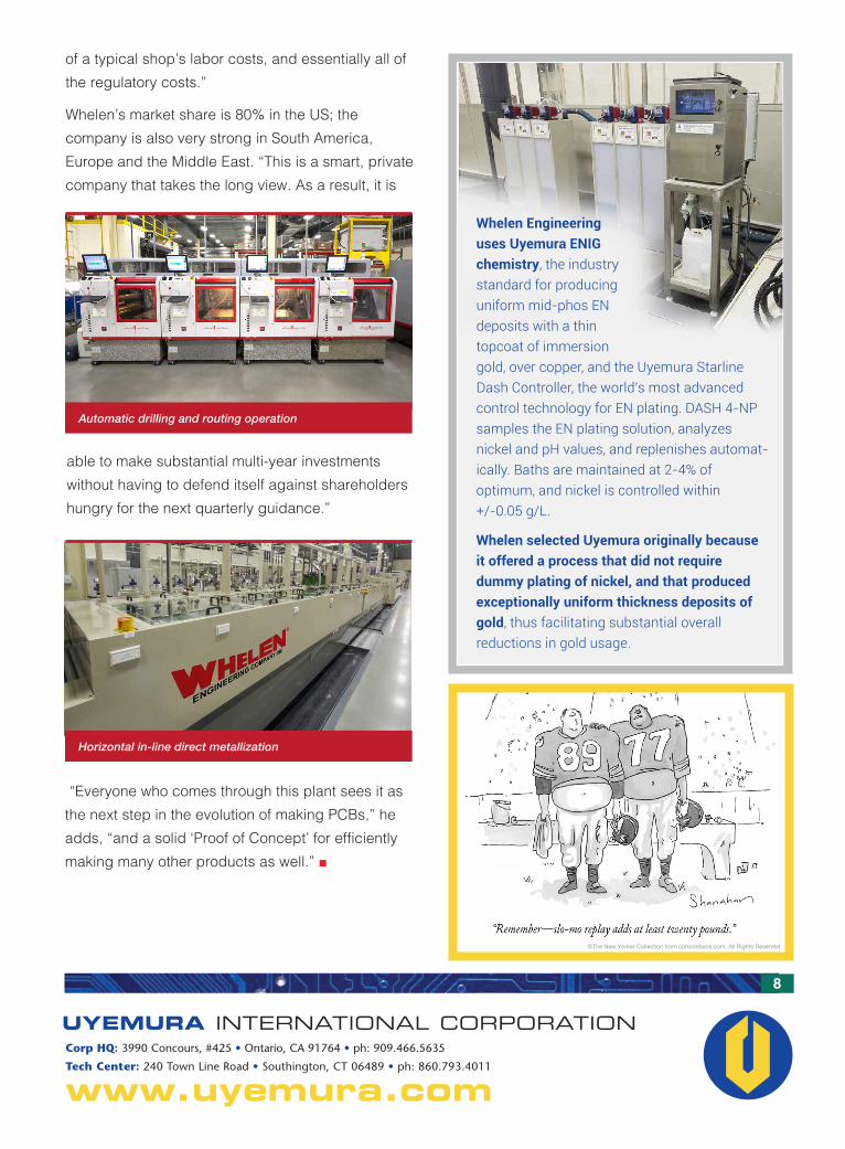
The production ramp is underway and expected to be completed shortly whereupon, Whelen Engi-neering will have 100% of its PCB production back in the USA – and bragging rights about achieving substantial cost savings over PCBs from China. “That includes both direct and indirect costs, as well as massive savings in cycle time,” says Stepinski. “We expect to be the first shop in the west to out-compete the Asia-Pacific region on direct PCB price per square inch.”
It is also the first totally “green” pcb shop. Explains Stepinski, “there is no need for wastewater permits, or air permits; liquid is 100% recycled, and we designed-out all of the air toxics.” A non-regulated resist stripper was developed as well. “We use just 500 gallons of fresh water a day to compensate for humidity loss from our air scrubber (which runs on recycled DI water to maximize absorption efficiency), and we have the first in the world, closed
imaging integration has, however, produced the most profound benefit in terms of labor savings. In addition, one worker manages the copper plate, metallization, tin plater, etch, resist, and tin stripping operations. “Our solder mask inkjet-based process is the only one in the world which also plugs the boards simultaneously with coating.”
China and Korea are today’s LCC (Low Cost Country) manufacturers for PC boards of all types.
In 2012, Whelen Engineering (Chester, CT and Charlestown, NH) was among the tens of thousands of OEMs that sourced their PCBs from Asia. Then, a perfect storm of intellectual property issues, lengthening lead times and increasing cost led the company to build - greenfield and-in-house – America’s first new rigid PCB shop in 15 years.
Whelen Engineering is a leading manufacturer of safety lighting and sirens for automotive, aviation and emergency warning applications. Their about-face in how they source the brains for every product they sell tells an important story about the power of innovation, the merits of questioning common wisdom, and how both of these can generate a Proof of Concept with implications far beyond one manufacturing operation.
Whelen was founded (in 1952) on the pillars of advanced production equipment, a motivated
workforce, and a commitment to vertical manufac-turing initiatives. In 2012, the company’s visionary CEO, John Olson, launched a new project that would take that vertical integration to an entirely new level.
“We also wanted an ROI of no more than 5 years, and although the industry minimum average headcount for a facility of this scale is 100 workers, we wanted to achieve everything with a workforce of no more than 17 total employees.”
Stepinski completed his initial design/business plan in 6 weeks: a unique U-shaped configuration 550’ long, with a 4.5 hour cycle time on a 50,000 sq-ft overall footprint.
A 2-level command center is elevated 12’ above the line. The first level is a chem lab, where one technician does wet process and cross-sectional analysis testing for the entire facility, in 6 hours per day. Both levels also house banks of monitors that track the temperature, concentration and level of every chemical, and the progress of each order. The line uses 39 pieces of automation linking 24 value-added process steps.
“We are really focused on lean concepts of waste reduction,” Stepinski continues. “Chemistry is stored in vented day tanks, with sensors monitoring levels and checking for leaks. Live inventory data is
database, pulling information relevant for that job, and processes it, from deburr thru final finish, in 4.5 hours and reports. Location/status is reported in real time via hundreds of its in-line sensors. “There is a 3% max coefficient of variation in plated surface copper thickness; the etch sytem has a maximum 1.5% variation in etch rate. This consistency allows us to run just one plating recipe, and one etching recipe, throughout the factory.”
The only stage where recipes change is in the imaging equipment. “This imaging equipment is first in the world, all digital inkjet technology,” says Stepinski. “We do digital inkjet printing for print and etch of the inner layers and metal core products, as well as for plate and etch of the outerlayers. For plate and etch, we panel plate all outerlayers and subcomposites with horizontal copper plating; however, we then tin plate the final etch resist so we have a ‘plate and etch’ process
with an inkjet resist.” Soldermask and legend processes are also inkjet. “This eliminates costly steps in photolithography: we don’t have a laminator or developer for primary imaging, nor a cleaner, microetch, or pre-dip for etch resist electro-plating.
“Additonally, our tin plater is so robust, we can afford to plate only 2.2-2.9 microns of tin on the surface.”
Due to this low thickness, 2 spray bars at 1.5 meters per minute are all that is needed to strip the tin after etching. “We only use a drum of standard tin strip chemistry every 16,000 panels, and a drum of tin brightener every 42,000 panels. A drum of resist stripper lasts for 14,000 panels with our wax-based inkjet ink.”
The most difficult process to integrate in the line was the imaging technology, which is markedly different from what’s been done previously. “We had to work with our suppliers and take it from an idea to a production process in a very short time.” The
A thorough analysis of current product designs and roadmap tolerance requirements was used to establish process spec targets.
“Extensive experimentation with large quantities of test panels was also required to adjust the plating thickness variation to the required level across our entire product mix. But by designing it all up-front, and systematically qualifying it, we now have a robust, predictable, low maintenance process for many years to come.”
Process controls were qualified to the point that no test panels are needed to interrupt production to qualify different product recipes, nor are any dummy panels required to compensate for current density edge effects. Whelen’s metallization process is “green” and based upon conductive polymer.
The system was designed so there’s no need to vent ammonia etch. “By performing the oxidation reaction offline in a separate sealed reactor, we’ve created a totally closed system.” Rinses are regenerated with a proprietary process as well. Virtually no hazwaste is generated (overall hazwaste volume as a stand-alone PCB shop meets the conditions of a small quantity generator, the company is regulated at a higher level).
Whelen was able to ‘design-out’ pollution concerns because the factory and waste treatment were a single, integrated design. “Our operating costs for waste treatment are far below conventional systems, and even our capital investment in waste treatment was below average for a shop our size” says Stepinski.
“There are practically no treatment chemicals used, except for minute amounts of acid and caustic. The high level of recycling that we do actually offsets most of the operating costs of our environmental systems. On a per-panel basis, conventional factories spend more money on fresh water than we spend on all of our combined regulatory operations.”
The manufacturing model developed for PCBs by Whelen Engineering is a Proof of Concept that’s applicable, in the company’s view, for many products. “The key,” says Stepinski, “is not just automation of a single piece of equipment, (in operations like drilling, plating, imaging, etc.), but
the combining of new technologies, such as inkjet and others, and the use of new, more efficient, more integrated process equipment.”
The Whelen model is a new solution that addresses this competitive advantage by engineering the integration of different processes to a new level of efficiency according to Stepinski. “The majority of the cost of quality in manufacturing boards is non-valued waste stemming from a lack of inter-process integration. This can be up to 80-90%
of a typical shop’s labor costs, and essentially all of the regulatory costs.”
Whelen’s market share is 80% in the US; the company is also very strong in South America, Europe and the Middle East. “This is a smart, private company that takes the long view. As a result, it is
loop recycling system for ammonia etchant.” It covers every waste aspect of the system. “We plate the copper out of the etchant, and rather than ammonium chloride for etching, we use a cocktail of ammonium sulfate and other low cost generic compunds, which we developed in partnership with a supplier to plate out the copper.
“We sell the 99.9% pure copper to a local recycler, and do not add any fresh chemicals to the etcher (chemicals were only needed for initial makeup). Our plating chemistry supplier has even approved the copper quality from the etcher for reuse in the plater, which will allow us to take copper that is removed at etch to be redissolved in the plater.
“This reduced our overall raw copper purchases by 95%, and allowed us to metallize the circuit pattern using waste copper from the laminate.”
continuously available. Tanks are sized for 3X supply chain average lead time. Our day tank system also reduces the number of manual chemical transactions by 99% versus a conven-tional facility by eliminating the hazardous, labor-intensive manual adds from the partially used drums. All adds are made via an HMI interface controlling metering pumps with safety interlocks. Laminate, masks and other solid materials are also stored in highly visible locations, with no central inventory.”
At the start of production, drilled panels are placed in a tray, which is barcoded; the tray then pings the
“Everyone who comes through this plant sees it as the next step in the evolution of making PCBs,” he adds, “and a solid ‘Proof of Concept’ for efficiently making many other products as well.”
Automatic drilling and routing operation
Horizontal in-line direct metallization
At the time, Whelen Engineering was spending millions of dollars each year on PCBs from China; prices and lead times were both on an upward trajectory. Injection molding and other critical operations had already been brought in-house, with results exceeding forecasts. A strategic decision was made to explore whether board making could be next.
In Spring 2013, management recruited Alex Stepinski, whose experience included senior engineering and management roles at large North American PCB Fab companies to develop a plan. He was, in his words, “all about nonconventional approaches.”
“The idea,” explains Stepinski, “was to build a fully
automated operation based on our core principles
that would produce a higher quality PWB, at a lower
price, with shorter lead times than offshore. The takt requirement to achieve 100% reshoring was PC board output of 50 panels per hour; translating to 2500 per week of 18” X 24” and 21” X 24”, rigid and rigid-flex panels; with capacity to expand up to 10,000 panels per week over the next decade.
able to make substantial multi-year investments without having to defend itself against shareholders hungry for the next quarterly guidance.”
Whelen Engineering uses Uyemura ENIG chemistry, the industry standard for producing uniform mid-phos EN deposits with a thin topcoat of immersion gold, over copper, and the Uyemura Starline Dash Controller, the world’s most advanced control technology for EN plating. DASH 4-NP samples the EN plating solution, analyzes nickel and pH values, and replenishes automat-ically. Baths are maintained at 2-4% of optimum, and nickel is controlled within +/-0.05 g/L.
Whelen selected Uyemura originally because it offered a process that did not require dummy plating of nickel, and that produced exceptionally uniform thickness deposits of gold, thus facilitating substantial overall reductions in gold usage.
8