Fabrication and Analysis of a Planar Junctionless Transistor
Upload
independentCategory
view
1download
0
NANO EXPRESS Open Access
Organic nanofibers integrated by transfertechnique in field-effect transistor devicesLuciana Tavares*, Jakob Kjelstrup-Hansen, Kasper Thilsing-Hansen and Horst-Günter Rubahn
Abstract
The electrical properties of self-assembled organic crystalline nanofibers are studied by integrating these on field-effect transistor platforms using both top and bottom contact configurations. In the staggered geometries, wherethe nanofibers are sandwiched between the gate and the source-drain electrodes, a better electrical conduction isobserved when compared to the coplanar geometry where the nanofibers are placed over the gate and thesource-drain electrodes. Qualitatively different output characteristics were observed for top and bottom contactdevices reflecting the significantly different contact resistances. Bottom contact devices are dominated by contacteffects, while the top contact device characteristics are determined by the nanofiber bulk properties. It is foundthat the contact resistance is lower for crystalline nanofibers when compared to amorphous thin films. Theseresults shed light on the charge injection and transport properties for such organic nanostructures and thusconstitute a significant step forward toward a nanofiber-based light-emitting device.
BackgroundIn the last decade, much attention has been given toone-dimensional nanostructures due to their intriguingphysics and in particular their application potentialwithin for example electronics and optoelectronics [1-3].Inorganic semiconducting crystalline nanowires madefrom, e.g., Si or III-V materials have been the focus ofmuch research due to the ability to synthesize these inlarge numbers with well-defined properties, which hasled to the demonstration of nanowire field-effect transis-tors [4,5], multicolor light sources [6], lasers [7], photodetectors [8,9], and solar cells [10,11].Today, however, the interest in alternative materials to
the more conventional inorganic semiconductors isincreasing. One example is organic materials based onsmall molecules, which similarly can be self-assembledinto crystalline nanostructures. This can be done eitherfrom solution [12,13] or by vapor deposition [14,15].One of the main features of this class of material is itsinherent tunability through chemical synthesis of themolecular building blocks [16], which enables the tailor-ing of the material properties for a specific applicationsuch as modification of the color of the luminescenceoutput [17,18]. In addition, the optical and electrical
properties [19] combined with low costs and fairlystraight-forward processing (also on flexible substrates[12]) make these materials interesting candidates fornanoscale optoelectronic and photonic devices applica-tions. The organic semiconductor para-hexaphenylene(p6P) can self-assemble into crystalline nanofibers struc-tures that emit polarized, blue light upon UV excitation[20], and it has been shown to work as light-emittingmaterial in organic light-emitting field-effect transistors(OLEFETs) [21].A remaining challenge, however, is the integration of
such organic nanofibers into the necessary surroundingcircuitry such as metal electrodes for electrical biasing.Essentially, two different strategies can be used: (1) anin situ growth approach, in which the nanostructure isself-assembled directly on the device platform to estab-lish the required electrical connections, and (2) a con-trolled transfer approach, in which pre-fabricatednanostructures are transferred to a device substrate forelectrical wiring. Both strategies have been demonstratedon a wafer scale for inorganic nanowires [22,23], and wehave recently demonstrated that the in situ growthapproach is also possible for organic nanofibers [24],although with a nanofiber morphology that is inferior toepitaxially grown fibers. The transfer strategy is difficultto implement due to the fragility of the van-der-Waals-bond crystals. Previously, it was demonstrated how a
* Correspondence: [email protected], Mads Clausen Institute, University of Southern Denmark, Alsion 2,DK-6400 Sønderborg, Denmark
Tavares et al. Nanoscale Research Letters 2011, 6:319http://www.nanoscalereslett.com/content/6/1/319
© 2011 Tavares et al; licensee Springer. This is an Open Access article distributed under the terms of the Creative Commons AttributionLicense (http://creativecommons.org/licenses/by/2.0), which permits unrestricted use, distribution, and reproduction in any medium,provided the original work is properly cited.
few nanofibers could be transferred by a drop-castingtechnique and connected electrically to metal contactsfor electrical two-point measurements, but this methodwas very time-consuming, with a low yield, and withloss of the parallel alignment [25].In this study, we report results from a study of the
electrical properties of p6P nanofibers implemented indifferent field-effect transistor (FET) configurations. Thep6P nanofibers were first grown on a special growthsubstrate for epitaxial growth and then transferred to asilicon-based transistor platform. We have recentlydemonstrated in details how fast and large-scale transferof organic nanofibers from the growth substrate onto adevice platform enables an easy fabrication of a largenumber of devices (Tavares L, Kjelstrup-Hansen J,Rubahn H-G: Efficient Roll-on Transfer Technique forWell-Aligned Organic Nanofibers, submitted.) withoutdamaging the morphology and optical properties of thefragile p6P nanofibers. Since the electrical characteristicsof organic FETs are known to depend on the exact tran-sistor geometry [26], we have studied three transistorgeometries: bottom contact/bottom gate (BC/BG), bot-tom contact/top gate (BC/TG), and top contact/bottomgate (TC/BG) [26,27]. The BC/BG configuration is froma device fabrication point-of-view the easiest geometry,since no further processing is required after transfer ofthe organic material onto the device platform, whileboth the BC/TG and the TC/BG require additionaldeposition steps to form the top gate or the top con-tacts, respectively. However, the two latter geometries(known as the staggered configurations) usually exhibitsuperior device performance. This behavior is assumedto be due to the fact that the charges are injected notonly from the edge of the electrodes (the case for acoplanar geometry) but also from the surface of thecontacts [26].
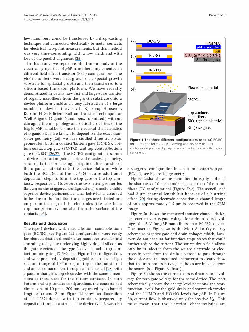
Results and discussionThe type 1 devices, which had a bottom contact/bottomgate (BC/BG, see Figure 1a) configuration, were readyfor characterization directly after nanofiber transfer andannealing using the underlying highly doped silicon asthe gate electrode. The type 2 devices had a top con-tact/bottom gate (TC/BG, see Figure 1b) configuration,and were prepared by depositing gold electrodes in highvacuum (range of 10-6 mbar) on top of the transferredand annealed nanofibers through a nanostencil [28] witha pattern that gives top electrodes with the same dimen-sions as those used for the bottom contacts. In bothbottom and top contact configurations, the contacts haddimensions of 10 μm × 200 μm, separated by a channellength of around 2 μm. Figure 1d shows an illustrationof a TC/BG device with top contacts prepared bydeposition through a stencil. The device type 3 was also
a staggered configuration in a bottom contact/top gate(BC/TG, see Figure 1c) geometry.Figure 2a,b,c show the nanofibers integrity and also
the sharpness of the electrode edges on top of the nano-fibers (TC configuration) (Figure 2b,c). The stencil usedhad 2 μm channel length but because of a blurringeffect [29] during electrode deposition, a channel lengthof only approximately 1.5 μm is observed in the SEMimage.Figure 3a shows the measured transfer characteristics,
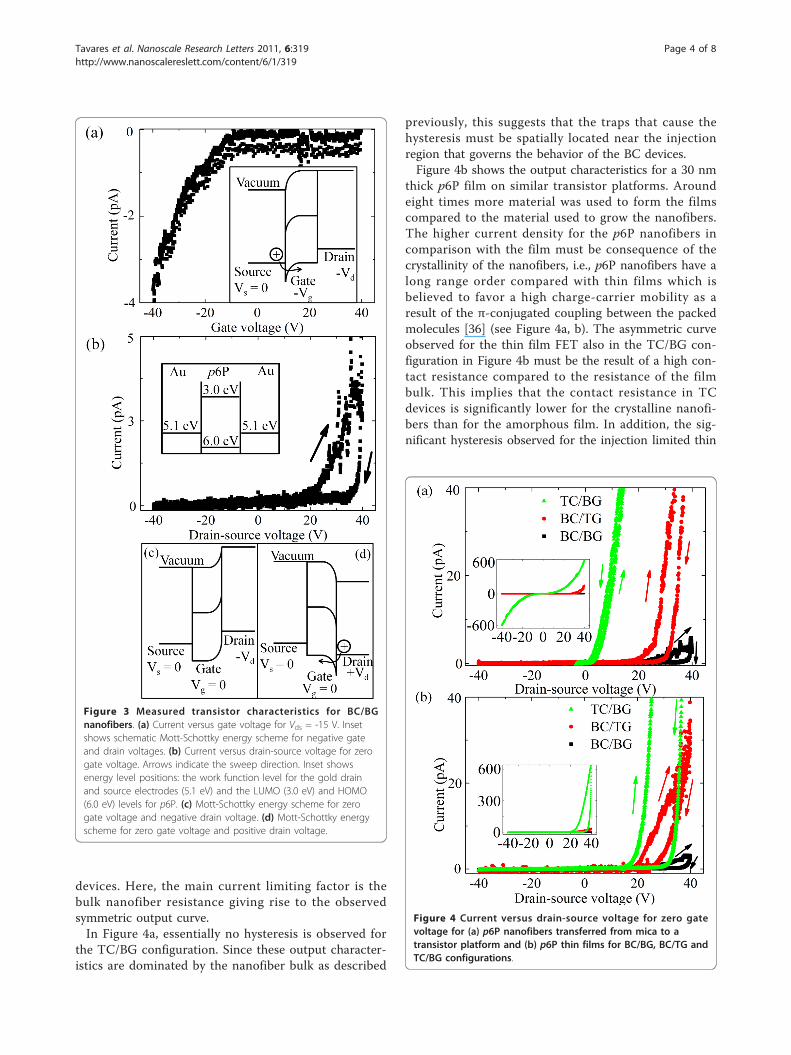
i.e., current versus gate voltage for a drain-source vol-tage of -15 V for p6P nanofibers on a BC/BG device.The inset in Figure 3a is the Mott-Schottky energyscheme at negative gate and drain voltages which, how-ever, do not account for interface traps states that couldfurther reduce the current. The source-drain field allowsonly holes injected from the source electrode or elec-trons injected from the drain electrode to pass throughthe device and the measured characteristics clearly showthat the transport is p-type, i.e., holes are injected fromthe source (see Figure 3a inset).Figure 3b shows the current versus drain-source vol-
tage for zero gate voltage for the same device. The insetschematically shows the energy level positions: the workfunction levels for the gold drain and source electrodesand the LUMO and HOMO levels for p6P. In Figure3b, current flow is observed only for positive Vds. Thismust mean that the electrical characteristics are
Figure 1 The three different configurations used: (a) BC/BG,(b) TC/BG, and (c) BC/TG. (d) Drawing of a device with TC/BGconfiguration prepared by deposition of the top contacts through ananostencil.
Tavares et al. Nanoscale Research Letters 2011, 6:319http://www.nanoscalereslett.com/content/6/1/319
Page 2 of 8

dominated by an injection barrier between the injectingmetal electrode and the organic material. This is notunexpected given the energy levels shown in the insetthat suggest an injection barrier for holes of around0.9 eV. As shown in Figure 3d, a positive Vds then leadsto downward band bending near the drain electrode andthereby a lowering of the hole injection barrier, while anegative Vds does not cause a similar band bending atthe source electrode as would be required for hole injec-tion in the opposite direction since the band bendingagain occurs at the drain electrode (see Figure 3c).A hysteresis effect can also be observed in Figure 3b
where the forward sweep is higher than the reversesweep. This is assumed to be caused by trapping of thecharge carriers [26,30,31]. We propose that the observedhysteresis is due to hole trapping close to the interfaceregion between the injecting electrode and the organicmaterial creating a space charge that reduces the bandbending and thereby limits further hole injection, caus-ing a lower back sweep current. We will elaborate onthis aspect below.Figure 4a shows current versus drain-source voltage
for zero gate voltage for transferred p6P nanofibers forBC/BG, BC/TG, and TC/BG configurations, while theinset shows the same data plotted with a different cur-rent scale. Considering that approximately the samenumber of nanofibers was present in all the samples, thecoplanar (BC/BG) configuration exhibits a lower outputcurrent than the staggered geometries due to a highcontact resistance associated with the high injection bar-rier to the organic material [32]. In the staggered geo-metries (BC/TG and TC/BG), the charges are injected
not only from the edge of the electrode but also fromthe surface of the contacts in the region where thesource-drain electrodes overlap with the gate electrodeand consequently charges are injected over a larger arealeading to a lower contact resistance than in the copla-nar (BC/BG) geometry [26].The TC/BG configuration exhibits the highest output
current. We propose that this is due to the smaller con-tact resistance between the nanofibers and the electro-des due to deposition of the electrodes under vacuum,which prevents water residues in the nanofiber-electrodeinterface in contrast to the bottom contact deviceswhere the nanofiber-electrode interface is created underhumid conditions during the transfer. As suggested byBao and co-workers [33], moisture residing at the inter-face between the electrode and the organic material isexpected to cause an increased contact resistance.Although our devices are annealed after fabrication, thiscan presumably not eliminate all water or water-trans-ferred contaminants residing at the interface, since hys-teresis is observed even after prolonged annealing. Also,metal penetrating into the organic material during elec-trode deposition can enable a better electrical contact[34,35].The symmetric characteristics of the TC/BG device as
opposed to the asymmetric behavior of the bottom con-nected devices can be observed in the inset of Figure 4a.Since no n-type behavior has been observed, this mustmean that in the TC/BG devices the source electrode isinjecting holes for negative drain-source voltages. Thesituation depicted in Figure 3c with band bending at thedrain electrode is thus not valid for the top contact
Figure 2 Nanofibers in top contacts configuration. (a) Fluorescence microscope image of nanofibers in the top contacts configuration.(b) White light microscope image of the sharp top contacts on nanofibers. (c) Scanning electron microscope image of the electrodesconnecting to the nanofibers as indicated in (b).
Tavares et al. Nanoscale Research Letters 2011, 6:319http://www.nanoscalereslett.com/content/6/1/319
Page 3 of 8
devices. Here, the main current limiting factor is thebulk nanofiber resistance giving rise to the observedsymmetric output curve.In Figure 4a, essentially no hysteresis is observed for
the TC/BG configuration. Since these output character-istics are dominated by the nanofiber bulk as described
previously, this suggests that the traps that cause thehysteresis must be spatially located near the injectionregion that governs the behavior of the BC devices.Figure 4b shows the output characteristics for a 30 nm
thick p6P film on similar transistor platforms. Aroundeight times more material was used to form the filmscompared to the material used to grow the nanofibers.The higher current density for the p6P nanofibers incomparison with the film must be consequence of thecrystallinity of the nanofibers, i.e., p6P nanofibers have along range order compared with thin films which isbelieved to favor a high charge-carrier mobility as aresult of the π-conjugated coupling between the packedmolecules [36] (see Figure 4a, b). The asymmetric curveobserved for the thin film FET also in the TC/BG con-figuration in Figure 4b must be the result of a high con-tact resistance compared to the resistance of the filmbulk. This implies that the contact resistance in TCdevices is significantly lower for the crystalline nanofi-bers than for the amorphous film. In addition, the sig-nificant hysteresis observed for the injection limited thin
Figure 3 Measured transistor characteristics for BC/BGnanofibers. (a) Current versus gate voltage for Vds = -15 V. Insetshows schematic Mott-Schottky energy scheme for negative gateand drain voltages. (b) Current versus drain-source voltage for zerogate voltage. Arrows indicate the sweep direction. Inset showsenergy level positions: the work function level for the gold drainand source electrodes (5.1 eV) and the LUMO (3.0 eV) and HOMO(6.0 eV) levels for p6P. (c) Mott-Schottky energy scheme for zerogate voltage and negative drain voltage. (d) Mott-Schottky energyscheme for zero gate voltage and positive drain voltage.
Figure 4 Current versus drain-source voltage for zero gatevoltage for (a) p6P nanofibers transferred from mica to atransistor platform and (b) p6P thin films for BC/BG, BC/TG andTC/BG configurations.
Tavares et al. Nanoscale Research Letters 2011, 6:319http://www.nanoscalereslett.com/content/6/1/319
Page 4 of 8

film devices further support our conclusion of the trapsbeing spatially located at the surface.In Figure 4a,b, a drain current saturation is not
observed. The channel length used was around 2 μmand the gate dielectric was 0.2 μm thick. It is well-known that if the channel length of a transistor is lessthan ten times the thickness of the gate dielectric, thespace-charge-limited bulk current will be dominated bythe lateral field due to the source-drain voltage prevent-ing saturation since the gate voltage will not determinethe charge distribution within the channel and conse-quently the “on” or “off” state of the transistor will notbe observed [26].Figure 5 shows the transfer characteristics, i.e., gate
voltage sweep at a certain Vds for both p6P thin filmsand nanofibers. Figure 5a shows that the nanofibersconduct better than the thin films (as mentioned pre-viously the film cross-sectional area is around eighttimes the nanofiber cross-section) and current satura-tion is not observed reinforcing the conclusion fromFigure 4.From Figure 5b, the subthreshold swings (S = dVg/d
(logIds)) [37] were obtained from the transfer
characteristics of the p6P nanofibers on different transis-tor configurations to elaborate on the switching behavior.From the data in Figure 5b, the subthreshold swing (S)
for the nanofibers on BC/BG, BC/TG, and TC/BG con-figurations were found to be 13.7, 9.5, and 7.5 V/decade,respectively. The TC/BG configuration exhibits the low-est subthreshold swing being almost half that of the BC/BG device. For comparison, Klauk et al. [38] have stu-died the electrical characteristics for pentacene transis-tors with 100 nm SiO2 as the gate dielectric and founda subthreshold swing of only 0.7 V/decade. Our resultsis around a decade above this, however, this is not unex-pected since the p6P mobility is significantly below thatfound in pentacene [21,38] and since our device geome-try (here particularly the gate dielectric thickness) wasnot optimized for efficient switching.
ConclusionsIn this study, we have for the first time demonstratedintegration of transferred organic nanofibers on differentfield-effect transistor platform configurations, which havebeen electrically characterized to reveal the significantdifferences in electrical performance between the differ-ent configurations. The coplanar device geometry has ahigh contact resistance and consequently a poor conduc-tion compared to the staggered geometries. Within thestaggered geometries, the top contact geometry showssuperior performance to the bottom contact geometrypresumably due to a cleaner interface between the con-tact and the organic material and due to metal penetra-tion into the organic material during contact deposition.The better electrical connection of the top contactsresults in the nanofiber transistor output characteristicsbeing dominated by the nanofiber bulk as opposed to thebottom contact devices which exhibit injection limitedbehavior. A direct comparison of the crystalline p6Pnanofibers with amorphous thin films shows that bothmaterials exhibit p-type behavior but the fibers conductsignificantly better owing to their better crystallinity.Such electrical contacted organic nanostructures can
have a range of applications, notably as nanoscaleorganic light emitters. These can be realized in similarfield-effect transistor configurations and are therefore anobvious next subject to be studied. The performance ofsuch organic transistors is influenced by a range of fac-tors and optimization can therefore be pursued forexample using other gate dielectrics [39], electrodematerials [40], and by implementing nanofibers fromother molecules [16].
MethodsNanofiber growthThe nanofibers were prepared by vapor depositionof p6P molecules under high vacuum conditions
Figure 5 Current versus gate voltage at Vds = -15 V for p6P(a)nanofibers and thin films in TC/BG configuration and (b) fornanofibers in BC/BG, BC/TG, and TC/BG configurations.
Tavares et al. Nanoscale Research Letters 2011, 6:319http://www.nanoscalereslett.com/content/6/1/319
Page 5 of 8
(p < 10-8 mbar) onto a heated muscovite mica substrate,which was cleaved in air before being immediately trans-ferred to the vacuum chamber. During deposition (rate0.1 Å · s-1), the substrate temperature was kept at463 K. This enables the surface diffusion of the mole-cules and molecular clusters, which then agglomerateand form long, surface-bound, mutually parallel nanofi-bers with macroscopic lengths (up to millimeters), andnanoscopic cross sections (widths hundred to severalhundred of nanometers and heights of several tens ofnanometers) [15]. The herringbone stacked molecules inthe fibers are oriented parallel to the substrate surface.The mean height and width of the nanofibers for 4 nmp6P deposition were around 40 and 250 nm, respec-tively, as determined by atomic force microscopy.
Nanofiber transfer techniqueThe integration of the nanofibers onto the device plat-form took place via a special transfer technique, thedetails of which will be reported elsewhere (Tavares L,Kjelstrup-Hansen J, Rubahn H-G: Efficient Roll-onTransfer Technique for Well-Aligned Organic Nanofi-bers, submitted.). In short, the mica substrate with thenanofibers was fixed on the sidewall of a transparentcylinder with an appropriate diameter. The transparencyof the cylinder helps to align the nanofibers to thedevice substrate and also to visualize when the mica andthe device substrate are in contact to perform the trans-fer process. The device substrate was placed on a softrubber platform to avoid compressing the nanofibersduring the transfer, and the nanofibers were transferredby rolling the cylinder with the nanofibers onto thedevice substrates under conditions of high humidity.After transfer, the chips were annealed at 80°C for20 min. This procedure was adopted to remove thewater adsorbed during the transferring process.
FET substrate preparationSilicon-based device substrates were used for integratingthe nanofibers with source, drain, and gate electrodes toform a field-effect transistor configuration. The sub-strates included elevated platforms that were used asreceiver platforms for the nanofibers in the subsequentnanofiber transfer step. These platforms, which had asize of 1000 μm × 200 μm, were lithographically pat-terned on a highly doped silicon substrate with 200 nmthermally grown SiO2 and realized first by HF etchingthrough the SiO2 layer followed by reactive ion etching1 μm into the silicon to give a total platform height of1.2 μm. On each receiver platform, two contact pads(390 μm × 180 μm) were prepared by photolithography,metal deposition (2 nm Ti/30 nm Au) and lift-off. Weprepared two different types of substrates to be able toprepare both bottom contact (BC) and top contact (TC)
devices. The TC device substrates were ready for nanofi-ber transfer after the preparation of the contact pads,while the BC substrates were processed additionallywith one more sequence of photolithography, metaldeposition (2 nm Ti/30 nm Au), and lift-off to formsmall, closely spaced electrodes, which were connectedto the large contact pads, and onto which the nanofiberscould be connected to span the gap. Gold was chosen asthe electrode material due to its inertness and due to itshigh work function (5.1 eV) that promotes hole injectioninto the nanofibers.The nanostencils were prepared from a 525 μm thick
silicon wafer coated with a 100 nm low-stress siliconnitride (SiN) layer. The electrode pattern was realized inthe frontside SiN layer by photolithography and reactiveion etching, and the membranes were released byphotolithography and etching from the wafer backsidein KOH solution (28 wt% KOH concentration at 80°Cfor approx. 9 h). A thin layer of photoresist was appliedon the wafer frontside to protect the fragile membranesbefore dicing. After the initial tests of electrode deposi-tion onto the nanofibers through the nanostencils, itwas observed that the photoluminescence spectrum ofthe p6P nanofibers had changed and the nanofibers hada pronounced green appearance as opposed to the clearblue color of “perfect” nanofibers. We attribute this tothe generation of defects in the nanofibers, which areknown to give rise to peaks in the green part of thespectrum [41]. This could indicate that the thin SiNmembrane shadow mask was too thin to protect thenanofibers against the radiation generated in the metaldeposition (electron beam evaporation) system. Thenanostencils were therefore coated with a thin metallayer to increase their ability to block the radiation thatis expected to damage the nanofibers, and the nanofi-bers that were contacted using these improved nanos-tencils now exhibited the correct spectral appearance.The top gate on BC/TG geometry was prepared byapplying 150 nm PMMA via spin-coating onto bottomcontacted nanofibers to function as gate dielectric andapplying a top gate electrode by gold deposition througha nanostencil with a suitable pattern (with dimensionsof 120 μm × 320 μm) on the PMMA layer and on topof the electrodes. Tests were also performed to confirmthe suitability of PMMA as gate dielectric by applyingPMMA on a clean device substrate with BG/BC config-uration. Here, no electrical conduction could beobserved. Previous investigations have also shown thatPMMA does not alter the p6P nanofibers’ electricalcharacteristics and that the original p6P spectrum is alsopreserved after coating [41]. For the TC and the TGdeposition, the alignment of the SiN stencil to thedevice substrate was done by hand under a white lightmicroscope.
Tavares et al. Nanoscale Research Letters 2011, 6:319http://www.nanoscalereslett.com/content/6/1/319
Page 6 of 8

In addition to the nanofiber devices, p6P thin film [42]devices were also prepared for comparison of the electri-cal properties of crystalline nanofibers and amorphousthin films. The preparation method was identical withthe exception of the nanofiber transfer step beingreplaced by vapor deposition of the p6P moleculesdirectly onto the device substrates at room temperatureresulting in a structure-less film.
CharacterizationThe completed devices were inspected using white lightmicroscopy, fluorescence microscopy (excitation wave-length of 365 nm), and scanning electron microscopy.The nanofiber dimensions were determined by tappingmode atomic force microscopy, and the field-effect tran-sistor characteristics were recorded with a probe stationand a labview-controlled characterization system basedon a data acquisition card and voltage and currentamplifiers.
AbbreviationsBC/BG: bottom contact/bottom gate; BC/TG: bottom contact/top gate; FET:field-effect transistor; OLEFETs: organic light-emitting field-effect transistors;TC/BG: top contact/bottom gate.
AcknowledgementsWe thank Henrik H. Henrichsen for valuable discussions.
Authors’ contributionsLT was involved in growing of the nanofibers and developing the FETsubstrates, made the transfer technique, transferred the nanofibers,performed the electrical measurements, contributed in the interpretation ofdata and drafted the manuscript. JKH developed the project, contributeddeveloping the FET substrates, analyzing the data, drafting the manuscriptand revised it, and have given final approval of the version to be published.KTH helped in growing of the nanofibers and developing the FET substrates.HGR revised it for important intellectual content.
Competing interestsThe authors declare that they have no competing interests.
Received: 27 January 2011 Accepted: 8 April 2011Published: 8 April 2011
References1. Yu G, Lieber CM: Assembly and integration of semiconductor nanowires
for functional nanosystems. Pure Appl Chem 2010, 82:2295-2314.2. Thelander C, Agarwal P, Brongersma S, Eymery J, Feiner LF, Forchel A,
Scheffler M, Riess W, Ohlsson BJ, Gösele U, Samuelson L: Nanowire-basedone-dimensional electronics. Mater Today 2006, 9:28-35.
3. Yang P, Yan R, Fardy M: Semiconductor Nanowire: What’s Next? Nano Lett2010, 10:1529-1536.
4. Thelander C, Mårtensson T, Björk MT, Ohlsson BJ, Larsson MW,Wallenberg LR, Samuelson L: Single-electron transistors in heterostructurenanowires. Appl Phys Lett 2003, 83:2052-2054.
5. Duan X, Huang Y, Cui Y, Wang J, Lieber CM: Indium phosphide nanowiresas building blocks for nanoscale electronic and optoelectronic devices.Nature 2001, 409:66-69.
6. Huang Y, Duan X, Lieber CM: Nanowires for Integrated MulticolorNanophotonics. Small 2005, 1:142-147.
7. Huang MH, Mao S, Feich H, Yan H, Wu Y, Kind H, Weber E, Russo R, Yang P:Room-Temperature Ultraviolet Nanowire Nanolasers. Science 2001,292:1897-1899.
8. Pettersson H, Trägårdh J, Persson AI, Landin L, Hessman D, Samuelson L:Infrared Photodetectors in Heterostructure Nanowires. Nano Lett 2006,6:229-232.
9. Soci C, Zhang A, Bao X-Y, Kim H, Lo Y, Wang D: Nanowire Photodetectors.J Nanosci Nanotechnol 2010, 10:1-20.
10. Tian B, Zheng X, Kempa TJ, Fang Y, Yu N, Yu G, Huang J, Lieber CM:Coaxial silicon nanowires as solar cells and nanoelectronic powersources. Nature 2007, 449:885-890.
11. Garnett E, Yang P: Light Trapping in Silicon Nanowire Solar Cells. NanoLett 2010, 10:1082-1087.
12. Briseno AL, Mannsfeld SCB, Lu X, Xiong Y, Jenekhe SA, Bao Z, Xia Y:Fabrication of Field-Effect Transistors from Hexathiapentacene Single-Crystal Nanowires. Nano Lett 2007, 7:668-675.
13. Tong Y, Tang Q, Lemke HT, Moth-Poulsen K, Westerlund F,Hammershøj P, Bechgaard K, Hu W, Bjørnholm T: Solution-BasedFabrication of Single-Crystalline Arrays of Organic Nanowires. Langmuir2010, 26:1130-1136.
14. Borras A, Aguirre M, Groening O, Lopez-Cartes C, Groening P: Synthesis ofSupported Single-Crystalline Organic Nanowires by Physical VaporDeposition. Chem Mater 2008, 20:7371-7373.
15. Balzer F, Rubahn H-G: Dipole-assisted self-assembly of light-emitting p-nPneedles on mica. Appl Phys Lett 2001, 79:3860-3862.
16. Schiek M, Balzer F, Al-Shamery K, Brewer JR, Lützen A, Rubahn H-G: OrganicMolecular Nanotechnology. Small 2008, 4:176-181.
17. Simbrunner C, Quochi F, Hernandez-Sosa G, Oehzelt M, Resel R, Hesser G,Arndt M, Saba M, Mura A, Bongiovanni G, Sitter H: Organic-OrganicHeteroepitaxy of Red-, Green-, and Blue-Emitting Nanofibers. ACS Nano2010, 4:6244-6250.
18. Park DH, Kim M-S, Cho EH, Park SH, Song H, Kim D-C, Kim J, Joo J:Luminescent Efficiency and Color for Poly(3-butylthiophene) NanowiresThrough Metal Coating: Color CCD Confirmation. Electrochem Solid-StateLett 2009, 12:K5-K8.
19. Balzer F, Madsen M, Kjelstrup-Hansen J, Schiek M, Rubahn H-G: OrganicNanowires. In Handbook of Nanophysics: Nanotubes and Nanowires. VolumeChap 21. Edited by: Sattler KD. Boca Raton: CRC Press; 2010:1-12.
20. Balzer F, Rubahn H-G: Growth Control and Optics of OrganicNanoaggregates. Adv Funct Mater 2005, 15:17-24.
21. Kjelstrup-Hansen J, Liu X, Henrichsen HH, Thilsing-Hansen K, Rubahn H-G:Conduction and electroluminescence from organic continuous andnanofiber thin films. Phys Stat Sol (C) 2010, 7:2763-2766.
22. Chen R-S, Wang S-W, Lan Z-H, Tsai JT-H, Wu C-T, Chen L-C, Chen K-H,Huang Y-S, Chen C-C: On-Chip Fabrication of Well-Aligned and Contact-Barrier-Free GaN Nanobridge Devices with Ultrahigh PhotocurrentResponsivity. Small 2008, 4:925-929.
23. Fan Z, Ho JC, Jacobson ZA, Yerushalmi R, Alley RL, Razavi H, Javey A: Wafer-Scale Assembly of Highly Ordered Semiconductor Nanowire Arrays byContact Printing. Nano Lett 2008, 8:20-25.
24. de Oliveira Hansen RM, Kjelstrup-Hansen J, Rubahn H-G: In situ-DirectedGrowth of Organic Nanofibers and Nanoflakes: Electrical andMorphological Properties. Nanoscale Res Lett 2011, 6:11, 1-5.
25. Henrichsen HH, Kjelstrup-Hansen J, Engstrøm D, Clausen CH, Bøggild P,Rubahn H-G: Electrical conductivity of organic single-nanofiber deviceswith different contact materials. Org Electron 2007, 8:540-544.
26. Zamuseil J, Sirringhaus H: Electron and Ambipolar Transport in OrganicField-Effect Transistors. Chem Rev 2007, 107:1296-1323.
27. Gundlach DJ, Zhou L, Nichols JA, Jackson TN, Necliudov PV, Shur MS: Anexperimental study of contact effects in organic thin film transistors. JAppl Phys 2006, 100:024509, 1-13.
28. Brugger J, Berenschot JW, Kuiper S, Nijdam W, Otter B, Elwenspoek M:Resistless patterning of sub-micron structures by evaporation throughnanostencils. Microelectron Eng 2000, 53:403-405.
29. Vazquez-Mena O, Villanueva LG, Savu V, Sidler K, Langlet P, Brugger J:Analysis of the blurring in stencil lithography. Nanotechnology 2009,20:415303, 1-10.
30. Egginger M, Bauer S, Schwödiauer R, Neugebauer H, Sariciftci NS: Currentversus gate voltage hysteresis in organic field effect transistors. MonatshChem 2009, 140:735-750.
31. Chua L-L, Zaumseil J, Chang F-J, Ou EC-W, Ho PK-H, Sirringhaus H,Friend RH: General observation of n-type field-effect behaviour inorganic semiconductors. Nature 2005, 434:194-199.
Tavares et al. Nanoscale Research Letters 2011, 6:319http://www.nanoscalereslett.com/content/6/1/319
Page 7 of 8
32. Appenzeller J, Knoch J, Derycke V, Martel R, Wind S, Avouris Ph: Field-Modulated Carrier Transport in Carbon Nanotube Transistors. Phys RevLett 2002, 89:126801, 1-4.
33. Li D, Borkent E-J, Nortrup R, Moon H, Katz H, Bao Z: Humidity effect onelectrical performance of organic thin-film transistors. Appl Phys Lett2005, 86:042105, 1-3.
34. Saudari SR, Lin YJ, Lai Y, Kagan CR: Device Configurations for AmbipolarTransport in Flexible, Pentacene Transistors. Adv Mater 2010,22:5063-5068.
35. Pesavento PV, Chesterfield RJ, Newman CR, Frisbie CD: Gated four-probemeasurements on pentacene thin-film transistors: Contact resistance asa function of gate voltage and temperature. J Appl Phys 2004,96:7312-7324.
36. Balakrishnan K, Datar A, Oitker R, Chen H, Zuo J, Zang L: Nanobelt Self-Assembly from an Organic n-Type Semiconductor: Propoxyethyl-PTCDI. JAm Chem Soc 2005, 127:10496-10497.
37. Guo Y, Yu G, Liu Y: Functional Organic Field-Effect Transistors. Adv Mater2010, 22:4427-4447.
38. Klauk H, Halik M, Zschieschang U, Schmid G, Radlik W, Weber W: High-mobility polymer gate dielectric pentacene thin film transistors. J ApplPhys 2002, 92:5259-5263.
39. Facchetti A, Yoon M-H, Marks TJ: Gate Dielectrics for Organic Field-EffectTransistors: New Opportunities for Organic Electronics. Adv Mater 2005,17:1705-1725.
40. Di C-a, Yu G, Liu Y, Xu X, Wei D, Song Y, Sun Y, Wang Y, Zhu D, Liu J, Liu X,Wu D: High-Performance Low-Cost Organic Field-Effect Transistors withChemically Modified Bottom Electrodes. J Am Chem Soc 2006,128:16418-16419.
41. Tavares L, Kjelstrup-Hansen J, Rubahn H-G, Sturm H: Reduced bleaching inorganic nanofibers by bilayer polymer/oxide coating. J Appl Phys 2010,107:103521, 1-6.
42. Gundlach DJ, Lin Y-Y, Jackson TN, Schlom DG: Oligophenyl-based organicthin film transistors. Appl Phys Lett 1997, 71:3853-3855.
doi:10.1186/1556-276X-6-319Cite this article as: Tavares et al.: Organic nanofibers integrated bytransfer technique in field-effect transistor devices. Nanoscale ResearchLetters 2011 6:319.
Submit your manuscript to a journal and benefi t from:
7 Convenient online submission
7 Rigorous peer review
7 Immediate publication on acceptance
7 Open access: articles freely available online
7 High visibility within the fi eld
7 Retaining the copyright to your article
Submit your next manuscript at 7 springeropen.com
Tavares et al. Nanoscale Research Letters 2011, 6:319http://www.nanoscalereslett.com/content/6/1/319
Page 8 of 8
Copyright © 2022 FDOKUMEN