Optoelectronic Neural Implant Sensors for Cerebral Blood ...
96
-
Upload
khangminh22 -
Category
Documents
-
view
3 -
download
0
Transcript of Optoelectronic Neural Implant Sensors for Cerebral Blood ...
Optoelectronic Neural Implant Sensors for Cerebral
Blood Volume Monitoring
Christopher Choi
Submitted in partial ful�llment of the
requirements for the degree
of Doctor of Philosophy
in the Graduate School of Arts and Sciences
COLUMBIA UNIVERSITY
2018

©2018
Christopher Choi
All Rights Reserved
Abstract
Optoelectronic Neural Implants for Cerebral Blood Volume
Monitoring
Christopher Choi
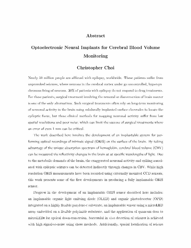
Nearly 50 million people are a�icted with epilepsy, worldwide. These patients su�er from
unprovoked seizures, where neurons in the cerebral cortex under go uncontrolled, hypersyn-
chronous �ring of neurons. 30% of patients with epilepsy do not respond to drug treatments.
For these patients, surgical treatment involving the removal or disconnection of brain matter
is one of the only alternatives. Such surgical treatments often rely on long-term monitoring
of neuronal activity in the brain using subdurally implanted surface electrodes to locate the
epileptic focus, but these clinical methods for mapping neuronal activity su�er from low
spatial resolutions and poor noise, which can limit the success of surgical treatments where
an error of even 1 mm can be critical.
The work described here involves the development of an implantable system for per-
forming optical recordings of intrinsic signal (ORIS) on the surface of the brain. By taking
advantage of the unique absorption spectrum of hemoglobin, cerebral blood volume (CBV)
can be measured via re�ectivity changes in the brain at at speci�c wavelengths of light. Due
to the metabolic demands of the brain, the exaggerated neuronal activity and spiking associ-
ated with epileptic seizures can be detected indirectly through changes in CBV. While high
resolution ORIS measurements have been recorded using externally mounted CCD sensors,
this work presents some of the �rst developments in producing a fully implantable ORIS
sensor.
Progress in the development of an implantable ORIS sensor described here includes:
an implantable organic light emitting diode (OLED) and organic photodetector (OPD)
integrated on a highly �exible parylene-c substrate, an implantable sensor using a microLED
array embedded on a �exible polyimide substrate, and the application of quantum dots to
microLEDs for optical down-conversion. Successful in vivo detection of seizures is achieved
with high signal-to-noise using these methods. Additionally, spatial localization of seizure

activity is performed using the microLED array. These developments represent crucial �rst
steps in the development of a full 2D neuronal mapping system using implantable ORIS
devices.
Contents
List of Figures iii
List of Tables x
1 Introduction 1
1.1 Epileptic Seizures . . . . . . . . . . . . . . . . . . . . . . . . . . . . . . . . . . 1
1.1.1 Seizure Propagation and Treatment . . . . . . . . . . . . . . . . . . . . 3
1.1.2 Mapping Neural Activity . . . . . . . . . . . . . . . . . . . . . . . . . 4
1.2 High Resolution Imaging . . . . . . . . . . . . . . . . . . . . . . . . . . . . . 5
1.3 Optical Recording of Intrinsic Signal (ORIS) . . . . . . . . . . . . . . . . . . 6
1.4 Objectives and Approach . . . . . . . . . . . . . . . . . . . . . . . . . . . . . 7
2 Basics of Flexible Optoelectronics 9
2.1 Introduction . . . . . . . . . . . . . . . . . . . . . . . . . . . . . . . . . . . . . 9
2.2 LEDs and Photodiodes . . . . . . . . . . . . . . . . . . . . . . . . . . . . . . . 9
2.3 Organic Semiconductors . . . . . . . . . . . . . . . . . . . . . . . . . . . . . . 12
2.3.1 Organic LED (OLED) . . . . . . . . . . . . . . . . . . . . . . . . . . . 14
2.3.2 Organic Photodetector (OPD) . . . . . . . . . . . . . . . . . . . . . . 17
2.3.3 Fabrication Methods . . . . . . . . . . . . . . . . . . . . . . . . . . . 19
2.3.4 Biomedical Applications for OLED and OPD . . . . . . . . . . . . . . 20
2.4 MicroLED . . . . . . . . . . . . . . . . . . . . . . . . . . . . . . . . . . . . . . 24
2.5 Colloidal Quantum Dots . . . . . . . . . . . . . . . . . . . . . . . . . . . . . . 29
2.5.1 Electroluminescent QDLEDs vs. Photoluminescent QDs . . . . . . . . 29
2.5.2 Biomedical Applications for Quantum Dots . . . . . . . . . . . . . . . 30
i

3 Integrated Organic LED and Organic Photodetector on a Highly Flexi-
ble Parylene-C Substrate 36
3.1 Highly �exible substrate . . . . . . . . . . . . . . . . . . . . . . . . . . . . . . 36
3.2 OLED and OPD Structure . . . . . . . . . . . . . . . . . . . . . . . . . . . . . 37
3.3 Fabrication . . . . . . . . . . . . . . . . . . . . . . . . . . . . . . . . . . . . . 39
3.4 Device Performance . . . . . . . . . . . . . . . . . . . . . . . . . . . . . . . . 40
3.5 In Vivo Measurement of Neural Activity and Detection of Seizures . . . . . . 44
3.6 Chapter Summary . . . . . . . . . . . . . . . . . . . . . . . . . . . . . . . . . 48
4 MicroLED Based Sensor 49
4.1 Bi-directional Emitter/Detector MicroLEDs . . . . . . . . . . . . . . . . . . . 49
4.2 Device Fabrication . . . . . . . . . . . . . . . . . . . . . . . . . . . . . . . . . 51
4.3 In-Vivo Measurement of CBV and Seizure Detection . . . . . . . . . . . . . . 53
4.4 MicroLED ORIS Sensor with Quantum Dot Optical Down-Conversion Coating 58
4.5 Chapter Summary . . . . . . . . . . . . . . . . . . . . . . . . . . . . . . . . . 62
5 Conclusion 63
Bibliography 66
Appendix 78
ii
List of Figures
1.1 Diagram of the cerebral hemispheres.[16] Image courtesy of blausen.com sta�
(2014). "Medical gallery of Blausen Medical 2014". WikiJournal of Medicine
1 (2). DOI:10.15347/wjm/2014.010. ISSN 2002-4436. Reused under the
Creative Commons Attribution 3.0 Unported license https://goo.gl/KfFFfo . 2
1.2 Schematic diagram of ECoG measurement using a subdurally implanted ar-
ray of surface electrodes.[16] Standard clinical surface electrodes can per-
form chronic measurement of neural activity, but have relatively low spa-
cial resolutions (< 1 cm). Image courtesy of: Blausen.com sta� (2014).
"Medical gallery of Blausen Medical 2014". WikiJournal of Medicine 1 (2).
DOI:10.15347/wjm/2014.010. ISSN 2002-4436. Reused under the Creative
Commons Attribution 3.0 Unported (CC BY 3.0) license https://goo.gl/KfFFfo
. . . . . . . . . . . . . . . . . . . . . . . . . . . . . . . . . . . . . . . . . . . . 5
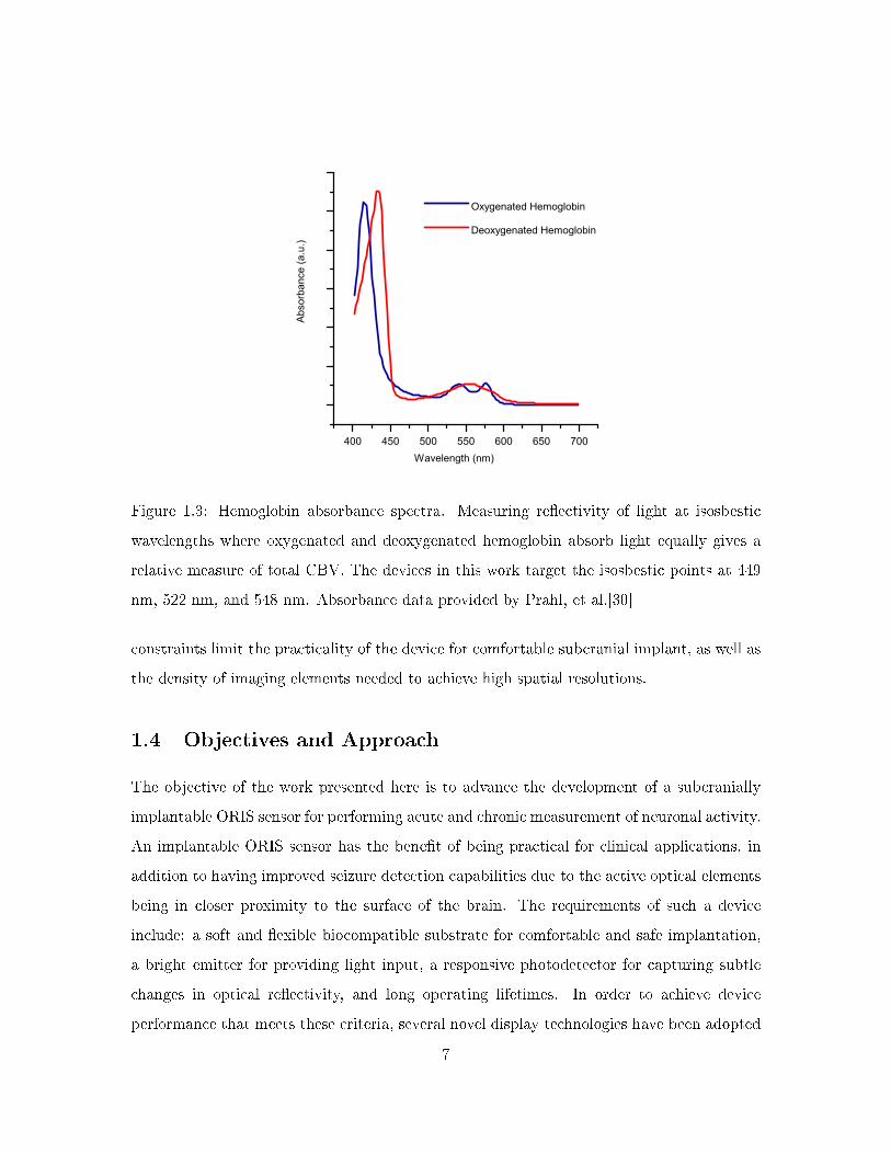
1.3 Hemoglobin absorbance spectra. Measuring re�ectivity of light at isosbestic
wavelengths where oxygenated and deoxygenated hemoglobin absorb light
equally gives a relative measure of total CBV. The devices in this work target
the isosbestic points at 449 nm, 522 nm, and 548 nm. Absorbance data
provided by Prahl, et al.[30] . . . . . . . . . . . . . . . . . . . . . . . . . . . . 7
2.1 Schematic showing the design and operation of an implantable ORIS sensor.
The primary elements include an LED and a photodetector integrated on a
thin, highly �exible substrate. . . . . . . . . . . . . . . . . . . . . . . . . . . 10
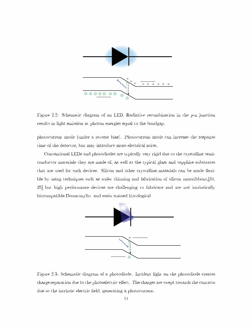
2.2 Schematic diagram of an LED. Radiative recombination in the p-n junction
results in light emission at photon energies equal to the bandgap. . . . . . . 11
iii
2.3 Schematic diagram of a photodiode. Incident light on the photodiode creates
charge separation due to the photoelectric e�ect. The charges are swept
towards the contacts due to the intrinsic electric �eld, generating a photocurrent. 11
2.4 The resonance forms of napthalene. The alternating double and single bonds
form conjugate pairs, with the extra electrons forming the double bonds not
having a speci�c localized orientation. This charge conjugation is the mech-
anism which gives rise to charge transport and semiconducting properties of
organic semiconductors. . . . . . . . . . . . . . . . . . . . . . . . . . . . . . . 13
2.5 Example of the band structure of an OLED. Recombination in the EML
results in green light emission whose wavelength is determined by the HOMO-
LUMO gap of AlQ3. . . . . . . . . . . . . . . . . . . . . . . . . . . . . . . . . 14
2.6 Diagram of singlet and triplet excited states. . . . . . . . . . . . . . . . . . . . 16
2.7 Photoexcitation and free charge conversion in a donor-acceptor junction. . . . 18
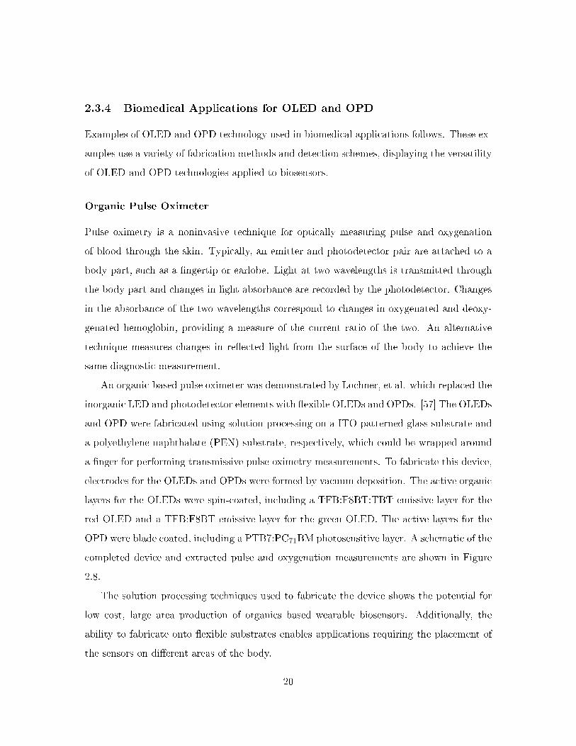
2.8 a) Organic pulse oximeter replaces inorganic optoelectronic elements with
OLEDs and OPDs (b) Hardware block diagram for the system including
ampli�cation and a microcontroller for data acquisition (c,d) Simultaneous
oximetry measurements with a commercially available inorganic oximeter
probe and the organic oximeter probe, respectively. Heart rate is determined
from the timing of the systolic peaks in the oximetry signals. The ratio of
transmitted light at two wavelengths was used to calculate blood oxygen satu-
ration using Beer�Lambert's law. [57] Reprinted by permission from Lochner,
Claire M., et al. "All-organic optoelectronic sensor for pulse oximetry." Na-
ture communications 5 (2014): 5745. . . . . . . . . . . . . . . . . . . . . . . . 21
2.9 Miniaturized biosensor using OPDs. [58] a) A glass slide with a printed
OPD sensor is used for CL detection of SEB b) The glass slide is placed
into a portable controller for data acquisition. Reprinted with permission
from Wojciechowski, Jason R., et al. "Organic photodiodes for biosensor
miniaturization." Analytical chemistry 81.9 (2009): 3455-3461. Copyright
2009 American Chemical Society." . . . . . . . . . . . . . . . . . . . . . . . . 22
iv
2.10 CL detection of SEB using an OPD. [58] Substrates treated with α-SEB,
SEB, and α-SEB-HRP were added ~20 s into recording. The concentration of
SEB detected measured in this plot was 5 ng/mL. Reprinted with permission
from Wojciechowski, Jason R., et al. "Organic photodiodes for biosensor
miniaturization." Analytical chemistry 81.9 (2009): 3455-3461. Copyright
2009 American Chemical Society." . . . . . . . . . . . . . . . . . . . . . . . . 24
2.11 Strain engineered �exible microLED display. [63] Reprinted by permission
from Byun, Junghwan, et al. "Fully printable, strain-engineered electronic
wrap for customizable soft electronics." Scienti�c Reports 7 (2017): 45328. . 26
2.12 Wireless optogenetic stimulation of mice using a microLED implant a) A
mouse implanted with the wireless blue microLED implant was con�ned to
an enclosure containing a resonant cavity for wireless power delivery. The
blue microLED was powered on wirelessly, triggering a circulatory motor
behavior induced by the activation of ChR2 b) Schematic of the wireless
microLED implant c) Photograph of the microLED implant [65] Reprinted
by permission from Montgomery, Kate L., et al. "Wirelessly powered, fully
internal optogenetics for brain, spinal and peripheral circuits in mice." Nature
methods 12.10 (2015): 969-974. . . . . . . . . . . . . . . . . . . . . . . . . . . 28
2.13 Schematic diagram of QDs used in targeted photodynamic therapy for tu-
mor suppression. [79] Reprinted from Biomaterials 34.4, Hsu, Chia-Yen, et
al., "Bioluminescence resonance energy transfer using luciferase-immobilized
quantum dots for self-illuminated photodynamic therapy.", Pages 1204-1212,
Copyright 2013, with permission from Elsevier. . . . . . . . . . . . . . . . . . 31
v
2.14 Tumor suppression via QD-enabled targeted photodynamic therapy.[79] a)
Tumor volume was tracked for the di�erent permutations of treatments. Mice
which received the BRET-induced photodynamic therapy showed a reduction
in tumor volume b) Stained sections of tumors c) Microscope image of tumors.
Reprinted from Biomaterials 34.4, Hsu, Chia-Yen, et al., "Bioluminescence
resonance energy transfer using luciferase-immobilized quantum dots for self-
illuminated photodynamic therapy.", Pages 1204-1212, Copyright 2013, with
permission from Elsevier. . . . . . . . . . . . . . . . . . . . . . . . . . . . . . 32
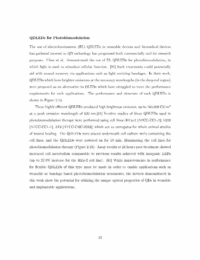
2.15 QDLED structure and performance. [81] a) Inverted QDLED structure b)
Emission spectrum of the EL QDLED. Insets show the structure of the QD
and a photograph of a completed QDLED c) Electroluminescent performance
of the QDLED reported d) The QDLED is a high e�ciency device capable
of high brightness. Reprinted by permission from Chen, Hao, et al. "Quan-
tum dot light emitting devices for photomedical applications." Journal of the
Society for Information Display 25.3 (2017): 177-184. . . . . . . . . . . . . . . 34
2.16 Photograph and schematic of the QDLED photobiomodulation therapy. [81]
a) Photograph of the red QDLED with 620 nm peak emission b) The QDLED
is placed underneath the transparent cell culture wells to perform in-vitro pho-
tobiomodulation therapy c) Schematic of the control experiment with no illu-
mination d) Schematic of the cell lines receiving photobiomodulation therapy
using a QDLED. Reprinted by permission from Chen, Hao, et al. "Quan-
tum dot light emitting devices for photomedical applications." Journal of the
Society for Information Display 25.3 (2017): 177-184. . . . . . . . . . . . . . . 35
3.1 Parylene-C Structure . . . . . . . . . . . . . . . . . . . . . . . . . . . . . . . . 37
3.2 Schematic of the OLED and OPD structure. A photograph showing the
layout of the OLED and OPD on the ORIS device is shown. . . . . . . . . . . 38
3.3 Fabrication of Organic Implantable ORIS Sensor . . . . . . . . . . . . . . . . 40
3.4 Flexible ORIS Sensor . . . . . . . . . . . . . . . . . . . . . . . . . . . . . . . . 41
3.5 OLED Emission Spectrum . The emission spectrum has a peak emission at
540 nm which overlaps with an isosbestic wavelength for hemoglobin. . . . . . 42
vi
3.6 Normalized Spectral Response of OPD . The 540nm isosbestic wavelength
used in the ORIS measurements is denoted with a dashed line. . . . . . . . . 42
3.7 OPD Photocurrent Response. The ON/OFF ratio between photocurrent gen-
erated under illumination and the background current under dark conditions
is over 1500 . . . . . . . . . . . . . . . . . . . . . . . . . . . . . . . . . . . . . 43
3.8 OLED Electrical Current and Light Output. With a bias voltage of 8.2 V,
the OLED outputs 5.6 µW of light, roughly 100 cd/m2. . . . . . . . . . . . . 43
3.9 OLED Operational Lifetime. The luminance half-life is marked with a dashed
line. The device has a lifetime over an hour when exposed to saline solution. 44
3.10 Photo of the organic ORIS device attached to the surface of the brain. The
OLED and OPD elements are circled in yellow, while the needle electrode is
marked by a green box. . . . . . . . . . . . . . . . . . . . . . . . . . . . . . . 45
3.11 Baseline variations in the CBV of the animal's brain recorded by the organic
ORIS device. The optical intrinsic (OI) signal captured by the organic ORIS
device is shown at the top with a fast Fourier transform (FFT) of the OI
shown directly below it. Isolated signals of SSHO, respiration, and heartbeat
are extracted from the OI signal by notch �ltering and plotted. . . . . . . . . 46
3.12 In vivo seizure detection using the organic ORIS device. The two plots at the
top show the LFP and OI signal recorded simultaneously during a sequence of
seizures. The duration of seizures is shaded in pink. A more detailed view of
a single seizure that occurred in the middle of the sequence is shown below.
The processed OI signal was produced by removing the oscillations due to
heartbeat and respiration, a signi�cant source of noise in detecting seizures. . 47
4.1 Photograph of the microLEDs soldered onto a glass substrate with a Cr/Au
circuit. DA1000 LED (left) is 1 mm in length. DA 850 (right) is 850 µm in
length. . . . . . . . . . . . . . . . . . . . . . . . . . . . . . . . . . . . . . . . . 49
4.2 Spectral response of the microLEDs . . . . . . . . . . . . . . . . . . . . . . . 50
vii
4.3 Fabrication steps for the microLED ORIS sensor. a) 40 nm Cr and then
150 nm Au are thermally evaporated onto a 25 µm thick, clean polyimide
sheet on a glass carrier. b) The circuit and bond pads are patterned via
photolithography and wet etching. c) Flux is applied to the bond pads and
the microLEDs are placed on the bond pads. The microLEDs are re�owed
in an infrared re�ow oven at 280 C. d) PMMA resist is deposited over the
bonded microLEDs using a pneumatic printer. The devices are annealed at
100 C for 90 minutes to harden the PMMA resist and remove the solvent.
e) Parylene-C is blanket-coated over the entire device after contacting the
devices hot bar bonding. f) The completed device is delaminated from the
glass carrier. . . . . . . . . . . . . . . . . . . . . . . . . . . . . . . . . . . . . 52
4.4 Photographs of the ORIS devices in operation. Left: Completed ORIS device
is shown with a blue microLED operating in emitter mode. Middle: ORIS
device �exed around a rod with 1/2 inch diameter. A green microLED is
shown operating at the same time. Right: MicroLED ORIS device attached
to the surface of a rat's brain. . . . . . . . . . . . . . . . . . . . . . . . . . . 52
4.5 Baseline Measurements of CBV by the microLED ORIS device. Left: ORIS
measurement of baseline CBV signals. Variations in the ORIS signal are due
to changes in CBV. Right: FFT of the baseline CBV signals. . . . . . . . . . 53
4.6 In vivo seizure detection using blue-to-green microLED ORIS device. Dura-
tion of seizures are shaded in pink. Seizures are detected with a signal-to-noise
ratio greater than 33 dB. SNR is determined by comparing the root mean
square amplitude of the baseline oscillations to the excursion in amplitude
during seizure events. . . . . . . . . . . . . . . . . . . . . . . . . . . . . . . . . 54
4.7 In vivo seizure detection using blue-to-blue microLED ORIS device. Duration
of seizures are shaded in pink. High SNR of seizure detection is achieved
despite the lower responsivity of the blue microLEDs. . . . . . . . . . . . . . 55
4.8 Layout of the linear array device. The two microLEDs in photodiode mode,
PD1 and PD2, are attached roughly 2 mm and 3.2 mm away from the focus
of the seizure which occurs at the site of 4AP injection. . . . . . . . . . . . . 57
viii
4.9 Localized measurements of CBV using a linear array of microLEDs. The
microLED detector labeled �PD2� is 1.2 mm further away from the focus of
the seizure than PD1. The duration of seizures at the epileptic focus are
highlighted in pink. Notch �ltering to remove the out of band signals is used
to improve the detection of seizures. . . . . . . . . . . . . . . . . . . . . . . . 57
4.10 Pneumatic printing QD optical down-conversion coatings. Photographs left
to right: pneumatic printing set up, green QD coating being applied to a
microLED, microLED with applied amber QD coating. . . . . . . . . . . . . . 59
4.11 Emission spectra for MicroLED coatings without �ltering. The blue com-
ponent of the emitted light is from microLED backlight that has not been
absorbed or has been back-re�ected from the substrate. . . . . . . . . . . . . 59
4.12 Emission spectra of optical QD down-conversion of blue microLED backlight.
Inset: photographs of the microLEDs with QD coatings shown operating.
Roscolux gel �lters and polyimide sheets are used to �lter any blue emission
not absorbed by the QDs. . . . . . . . . . . . . . . . . . . . . . . . . . . . . . 60
4.13 Seizure detection using a microLED ORIS device with green QD down-conversion
coating. Duration of seizures is highlighted in pink. Notch �ltering to remove
the out-of-band signals is used to improve the detection of seizures. . . . . . . 61
5.1 Diagram of 3 variants of CdS/CdSe/CdS core shell quantum dots. . . . . . . 80
5.2 QD absorption (left) and photoluminescent (right) spectra for 3 di�erent vari-
ants of CdS/CdSe/CdS core shell QDs suspended in toluene. . . . . . . . . . 80
ix

List of Tables
4.1 Responsivity of microLEDs in photodiode mode to 3 di�erent light emissions
used in the ORIS device. . . . . . . . . . . . . . . . . . . . . . . . . . . . . . . 51
x

Acknowledgements
I would like to acknowledge and thank my advisor, Professor Ioannis Kymissis, for his
mentorship and guidance on this project, my education, and my career. His passion for
technology and engineering innovation has inspired and driven me through my time at
Columbia. I am grateful for all the opportunities, lessons, and patients that he has provided.
I would also like to acknowledge and thank Professor Hongtao Ma, who I worked closely
with in completing this work.
I would like to acknowledge and thank Youngwan Kim, whose contributions, e�ort, time
dedicated to this work cannot be overstated.
Thank you to my family for their unwavering support and love. To Mom, Dad, Andrew,
Nathan, thank you for always believing in me. To my extended family, thank you for rooting
for me all these years.
Thank you to my friends, in New York and beyond. Special thanks go out to Ting-Ting
Zhou, E-dean Fung, and Wesley Chao for their aid in proofreading this document.
I would like to acknowledge the members of the committee for their time and feedback:
Professor Wen Wang, Professor Dion Khodagholy, and Professor Nanfang Yu.
I would like to acknowledge past and present members of CLUE. In particular, I would
like to thank Aida Raquel Colón-Berríos for your advice and expertise in the lab.
I would like to thank Dennis Wang for the countless dinners, co�ee breaks, and hours
spent studying together.
Finally, I would like to acknowledge the rats who gave their lives for the advancement
of science.
xi

Dedicated to Jenny Choi and Jae Kyu Choi
xii
Chapter 1
Introduction
Recent progress in �exible electronics and sensors have shown promise for enabling a new
class of wearable and implantable healthcare devices.[1, 2, 3, 4, 5, 6, 7, 8] By coupling
advanced hardware with novel computational methods to collect larger sets of data with
higher granularity than ever before,[9, 10, 11] it may be possible to greatly improve health-
care diagnostics and patient care, as well as our understanding of human physiology. One
application in particular that can greatly bene�t from advances in clinical hardware sensors
is the diagnosis and treatment of epilepsy.
1.1 Epileptic Seizures
Epilepsy is a chronic neurological disorder which a�icts nearly 50 million people worldwide.[12]
A patient is diagnosed with epilepsy when they have two or more unprovoked seizures that
are not the result of another medical condition such as fever or drug withdrawal. While
seizures can occur for a variety of reasons other than epilepsy, the causes for epilepsy itself
are not well understood, as each case of epilepsy has its own distinct history and response
to treatment.[13]
1
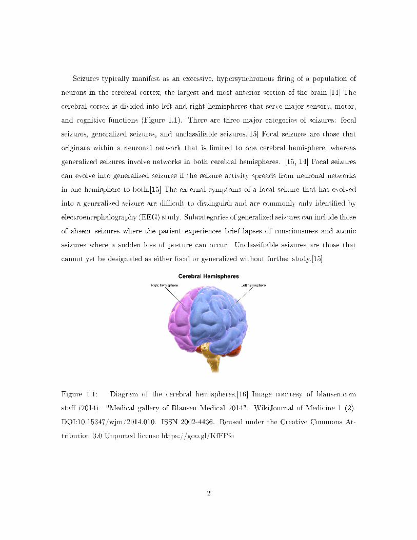
Seizures typically manifest as an excessive, hypersynchronous �ring of a population of
neurons in the cerebral cortex, the largest and most anterior section of the brain.[14] The
cerebral cortex is divided into left and right hemispheres that serve major sensory, motor,
and cognitive functions (Figure 1.1). There are three major categories of seizures: focal
seizures, generalized seizures, and unclassi�able seizures.[15] Focal seizures are those that
originate within a neuronal network that is limited to one cerebral hemisphere, whereas
generalized seizures involve networks in both cerebral hemispheres. [15, 14] Focal seizures
can evolve into generalized seizures if the seizure activity spreads from neuronal networks
in one hemisphere to both.[15] The external symptoms of a focal seizure that has evolved
into a generalized seizure are di�cult to distinguish and are commonly only identi�ed by
electroencephalography (EEG) study. Subcategories of generalized seizures can include those
of absent seizures where the patient experiences brief lapses of consciousness and atonic
seizures where a sudden loss of posture can occur. Unclassi�able seizures are those that
cannot yet be designated as either focal or generalized without further study.[15]
Figure 1.1: Diagram of the cerebral hemispheres.[16] Image courtesy of blausen.com
sta� (2014). "Medical gallery of Blausen Medical 2014". WikiJournal of Medicine 1 (2).
DOI:10.15347/wjm/2014.010. ISSN 2002-4436. Reused under the Creative Commons At-
tribution 3.0 Unported license https://goo.gl/KfFFfo
2
1.1.1 Seizure Propagation and Treatment
Focal seizures can typically initiate in localized regions of the cortex and propagate to
neighboring regions. According to Harrison's Principles of Internal Medicine, �The ini-
tiation phase is characterized by two concurrent events in an aggregate of neurons: (1)
high-frequency bursts of action potentials and (2) hypersynchronization. The bursting ac-
tivity is caused by a relatively long-lasting depolarization of the neuronal membrane due
to in�ux of extracellular calcium (Ca2+), which leads to the opening of voltage-dependent
sodium (Na+) channels, in�ux of Na+, and generation of repetitive action potentials. This
is followed by a hyperpolarizing afterpotential mediated by γ-aminobutyric acid (GABA)
receptors or potassium (K+) channels, depending on the cell type.�[15] With normal, healthy
neuronal activity, hyperpolarization and surrounding inhibitory neurons prevent the prop-
agation of the bursting activity; however, with su�cient activation by an increase of ion
concentrations, enhanced neurotransmitter release, excitation of amino acid receptors, or
stimulation of the neuronal tissue, neighboring neurons can be recruited for the propagation
of seizures to contiguous areas of the cortex or to distant areas via pathways such as the
corpus callosum.
The most common treatment method for epilepsy is through antiepileptic drug (AED)
therapy, with the primary goals of reducing the frequency or eliminating seizures to the
greatest extent possible, evading adverse side e�ects of long term treatment, and aiding
patients in maintaining normal social, vocational, and lifestyle function.[13] Typically, AED
therapy works by blocking the initiation or propagation of seizures.[15] The most common
drugs used for inhibiting epileptic seizures may achieve this by inhibiting Ca+ channels in
the neurons[13]or by increasing the presence of neurotransmitters that mediate synaptic
transmission, such as gamma aminobutyric acid (GABA).[13]
Unfortunately, approximately 30% of patients with epilepsy do not respond to anti-
epileptic drugs.[13, 14] For these patients, the unpredictability of seizures occurring dra-
matically impacts the quality of life for both patients and caregivers.[17] One of the only
alternative treatments for patients who are unresponsive to AED is epilepsy surgery which
removes or disconnects pathology sections of brain matter.
3
Patients are eligible for resective epilepsy surgery if the areas of the brain responsi-
ble for seizures are safe to remove without overly severe levels of disruption to neurological
function.[14, 15] In order to maximize the success of surgery, patient selection is critical. Sur-
geons employ thorough diagnostic tests including video and EEG monitoring, neuroimaging,
and neuropsychometric studies. [14] Once a patient has been selected for surgery, extensive
chronic study by neural imaging is required to identify the pathology areas of the brain and
develop a surgical treatment plan. Thus, the development of high �delity, high spatiotem-
poral resolution neural imaging capabilities are crucial for increasing the success of epilepsy
surgeries, as well as furthering the understanding of complicated neurological disorders like
epilepsy.
1.1.2 Mapping Neural Activity
Clinical practice currently measures neural activity via EEG and Electrocorticography (ECoG).
These techniques utilize a grid of surface electrodes which measure the electrical local �eld
potential of cortical neuronal dendrites near the brain's surface. The electrical signals are
conducted through the surface of the skull or cerebral cortex, for EEG and ECoG respec-
tively. When neuronal cells activate, the �ow of ions through the synapse creates a dipole
outside the dendrite. The oscillation of electric �eld potential due to these dipoles can then
be detected by the surface electrodes used in EEG and ECoG. While an EEG electrode
placed on the scalp is unable to pick up single neuron activity, they are able to detect the
potential changes due to clusters of thousands of neurons �ring synchronously. [14]
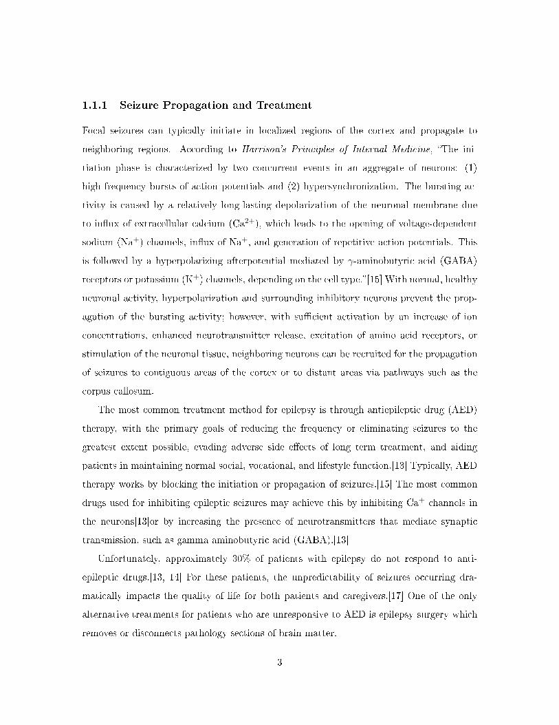
For surgical candidates, ECoG recorded with a subdurally implanted array of surface
electrodes covering a large surface of the brain is the standard of care for determining the
focus and propagation of seizures (Figure 1.2). Typical studies prior to surgery involve
long-term monitoring of neural activity with an implanted ECoG array lasting up to a few
weeks, in addition to acute studies involving short-term implantation coupled with neural
stimulation.[14, 15] While clinical ECoG measurements have improved resolution (typically
<1 cm and <1 ms) and signal-to-noise ratio (SNR) over EEG, a greater spatiotemporal
resolution and SNR of neural activity measurements would greatly aid treatment by surgical
resections where even small errors on the order of 1 mm can be signi�cant.[18]4

Figure 1.2: Schematic diagram of ECoG measurement using a subdurally implanted array of
surface electrodes.[16] Standard clinical surface electrodes can perform chronic measurement
of neural activity, but have relatively low spacial resolutions (< 1 cm). Image courtesy
of: Blausen.com sta� (2014). "Medical gallery of Blausen Medical 2014". WikiJournal of
Medicine 1 (2). DOI:10.15347/wjm/2014.010. ISSN 2002-4436. Reused under the Creative
Commons Attribution 3.0 Unported (CC BY 3.0) license https://goo.gl/KfFFfo
1.2 High Resolution Imaging
Standard clinical methods for high resolution imaging include magnetic resonance imaging
(MRI), positron emission tomography (PET), single photon emission computed tomography
(SPECT), and magnetoencephalography (MEG), and functional MRI (fMRI). [14] While
these techniques can produce maps of neural imaging with high spatial resolutions (< 1mm)
and are valuable for acute studies, these methods are not ideal for chronic studies as pa-
tient movement is restricted and functional dyes are required for some of the mentioned
techniques.
5
Research in the �eld of advanced ECoG has sought to improve the resolution and �-
delity of subdurally implanted surface electrode arrays with advances in both the sensing
hardware[19, 20, 21] and computational analysis[9] involved. For instance, recent work by
Khodagholy et al. has introduced a �exible, organic electronics-based array with interelec-
trode spacing as small as 23 µm.[20, 21] These advances coincide with recent progress in the
�eld of wearable and implantable �exible electronic sensors which holds much promise for
future advanced and personalized healthcare diagnostics. [22, 1, 6, 23, 7, 8, 24, 4]
1.3 Optical Recording of Intrinsic Signal (ORIS)
A promising alternative to ECoG imaging of neural activity is the optical recording of in-
trinsic signal (ORIS). ORIS monitors changes in optical signals associated with neuronal
activity.[25] By monitoring optical re�ectivity changes caused by cerebral blood volume
(CBV) and cerebral blood �ow (CBF), seizure events in the brain have been recorded with
high spatiotemporal resolution (<200 µm and <200 ms). [26, 27, 28, 29] By taking advan-
tage of the absorbance spectra of oxygenated and deoxygenated hemoglobin (Figure 1.3),[30]
total CBV can be recorded by measuring the re�ectivity of light at the isosbestic, or equal
absorption, wavelengths for hemoglobin. Since, the brain is tightly vasoregulated, seizure
events which induce exaggerated neuronal activity in localized regions of the brain are cor-
related with drastic changes in CBV and CBF that can be precisely mapped using ORIS.
Work by Suh et. al demonstrated 2D mapping of seizure activity with spatial resolutions
below 200 µm using a suspended CCD camera to capture re�ected ORIS signals.[29]
While ORIS can provide high spatiotemporal resolution imaging of seizure activity with-
out the need for harmful dyes, an ORIS measurement system for clinical and long-term
monitoring of neuronal activity has not been demonstrated. ORIS measurements using a
suspended camera require the patient to be stationary, with their brain exposed. Early
work in developing an implantable measurement system includes an ORIS sensor that uses
o�-the-shelf light emitting diodes and photodetectors integrated on a �exible substrate.[31]
This semi-�exible device is able to perform seizure detection by ORIS with high signal-to-
noise ratio (SNR), but is limited by the large dimensions of the components used. These
6
400 450 500 550 600 650 700
Abso
rban
ce (a
.u.)
Wavelength (nm)
Oxygenated Hemoglobin
Deoxygenated Hemoglobin
Figure 1.3: Hemoglobin absorbance spectra. Measuring re�ectivity of light at isosbestic
wavelengths where oxygenated and deoxygenated hemoglobin absorb light equally gives a
relative measure of total CBV. The devices in this work target the isosbestic points at 449
nm, 522 nm, and 548 nm. Absorbance data provided by Prahl, et al.[30]
constraints limit the practicality of the device for comfortable subcranial implant, as well as
the density of imaging elements needed to achieve high spatial resolutions.
1.4 Objectives and Approach
The objective of the work presented here is to advance the development of a subcranially
implantable ORIS sensor for performing acute and chronic measurement of neuronal activity.
An implantable ORIS sensor has the bene�t of being practical for clinical applications, in
addition to having improved seizure detection capabilities due to the active optical elements
being in closer proximity to the surface of the brain. The requirements of such a device
include: a soft and �exible biocompatible substrate for comfortable and safe implantation,
a bright emitter for providing light input, a responsive photodetector for capturing subtle
changes in optical re�ectivity, and long operating lifetimes. In order to achieve device
performance that meets these criteria, several novel display technologies have been adopted
7
for use in ORIS sensing. Two main device architectures presented here are: 1) an optical
sensor based on �exible organic light emitting diodes and organic photodiodes 2) an optical
sensor that utilizes microLEDs embedded on a �exible polyimide substrate with modi�cation
via quantum dot optical down-conversion.
8
Chapter 2
Basics of Flexible Optoelectronics
2.1 Introduction
This chapter reviews the basic operating principles of various �exible electronic and opto-
electronic technologies used in this work. The primary elements involved in the development
of an implantable ORIS sensor are a stable, bright emitter in the form of a light emitting
diode (LED) and a photosensitive detector. While the use of �exible LEDs has been exten-
sively studied for display and communication applications, the adoption of these devices for
biomedical sensing is relatively new. A schematic showing the basic operating principles of
an implantable ORIS sensor is shown in Figure 2.1.
2.2 LEDs and Photodiodes
Standard p-n junction diodes involve doped p-type semiconductor, where holes are the ma-
jority mobile charge carrier, abutted against an n-type material, where electrons are the
majority mobile charge carrier. At zero bias, a depletion region of space charge forms on
either side of the p-n interface due to charge di�usion. In the steady state, the electro-
static �elds from the space charge in the depletion region prevent further di�usion of charge
across the junction. In reverse bias, the depletion region is widened and practically no cur-
rent �ows, except at extreme voltages where device breakdown occurs. Under forward bias,
charge injection causes the depletion region to narrow, until a signi�cant amount of charge
9
Reflected
Signal
Light
Input
LED
EmitterPhotodetector
Figure 2.1: Schematic showing the design and operation of an implantable ORIS sensor.
The primary elements include an LED and a photodetector integrated on a thin, highly
�exible substrate.
is able to di�use across the junction at bias voltages above the threshold. Thus, current is
restricted to �ow in one direction across the diode.
LEDs operate similarly to standard p-n junction diodes, except that the recombination
that occurs at the interface between the n-type semiconductor and p-type semiconductor
under forward bias is radiative, resulting in the generation of photons (Figure 2.2). Since
LEDs are fabricated from mostly transparent materials, the light produced by recombination
at the interface, can escape. LEDs conventionally are made from direct band gap materials
like GaAs or GaN, which have higher probabilities of radiative recombination than indirect
band gap materials. The wavelength of light emitted by an LED is determined by the
bandgap of the emissive material where recombination occurs.
Photodiodes generally operate in reverse of LEDs. Light incident on the photosensi-
tive material generates charge separation which is collected by the anode and cathode of
the device. LEDs can operate like photodiodes, according to the Mims e�ect,[32, 33] but
have larger bandgaps which diminishes the available range of wavelengths for producing
photocurrent. Photodiodes can be operated in photovoltaic mode (no electrical bias) or
10
e- e- e- e-
e-
++++ + + +
e- e- e-
e-
+
+
Figure 2.2: Schematic diagram of an LED. Radiative recombination in the p-n junction
results in light emission at photon energies equal to the bandgap.
photocurrent mode (under a reverse bias). Photocurrent mode can increase the response
time of the detector, but may introduce more electrical noise.
Conventional LEDs and photodiodes are typically very rigid due to the crystalline semi-
conductor materials they are made of, as well as the typical glass and sapphire substrates
that are used for such devices. Silicon and other crystalline materials can be made �exi-
ble by using techniques such as wafer thinning and fabrication of silicon nanoribbons,[34,
35] but high performance devices are challenging to fabricate and are not intrinsically
biocompatible.Hematoxylin- and eosin-stained histological
e-
+
Figure 2.3: Schematic diagram of a photodiode. Incident light on the photodiode creates
charge separation due to the photoelectric e�ect. The charges are swept towards the contacts
due to the intrinsic electric �eld, generating a photocurrent.
11
2.3 Organic Semiconductors
One method of producing �exible electronics devices is to utilize organic semiconducting
materials. Organic semiconductors are comprised of organic (containing carbon) small
molecules or polymers and have the advantage of being intrinsically �exible, partly due
to the thin nature of most organic electronic devices, with the total thickness of the active
materials typically under 1 µm ). Due to the fact that bonds between organic molecules tend
to be weak, often formed by van der Waals interactions, thermal budgeting for processing
and fabricating thin �lm organic semiconductors is low.[36] Therefore, organic semiconduc-
tor devices can be fabricated on almost any substrate, including plastics that cannot handle
the intense thermal processing needed for many inorganic crystalline semiconductors. Or-
ganic semiconductors can even be fabricated by solution processing, an area of great interest
for applications such as roll-to-roll processing and large area fabrication.[36]
Charge transport in organic semiconductors typically occurs via chains or sheets of sp2-
hybridized carbon. The electronic con�gurations of carbon atoms in organic semiconductors
often form hybrid sp molecular orbitals which collectively have a lower energy than if the
carbon molecules remained in their neutral valence electron con�guration (2s2, 2p2). Shared
sp2 orbitals in carbon-carbon bonds form what are known as σ-bonds which are strong and
highly directional.[36] Perpendicular to the axis of the σ-bonds, electrons in the weakly
associated pz, or π, orbitals of the hybridized carbon form what are known as conjugated
π-bonds. These delocalized π-electrons can organize into multiple electronic con�gurations
for a single type of molecule; an example of this is napthalene whose conjugated bonds are
depicted as alternating single and double bonds in Figure 2.4. These delocalized charge
carriers in the π-bonds allow for charge transport in organic semiconductors.
12
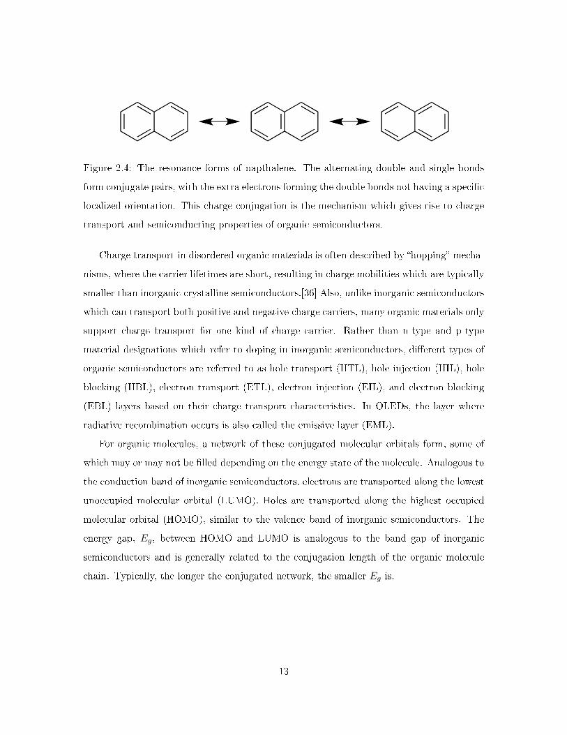
Figure 2.4: The resonance forms of napthalene. The alternating double and single bonds
form conjugate pairs, with the extra electrons forming the double bonds not having a speci�c
localized orientation. This charge conjugation is the mechanism which gives rise to charge
transport and semiconducting properties of organic semiconductors.
Charge transport in disordered organic materials is often described by �hopping� mecha-
nisms, where the carrier lifetimes are short, resulting in charge mobilities which are typically
smaller than inorganic crystalline semiconductors.[36] Also, unlike inorganic semiconductors
which can transport both positive and negative charge carriers, many organic materials only
support charge transport for one kind of charge carrier. Rather than n-type and p-type
material designations which refer to doping in inorganic semiconductors, di�erent types of
organic semiconductors are referred to as hole transport (HTL), hole injection (HIL), hole
blocking (HBL), electron transport (ETL), electron injection (EIL), and electron blocking
(EBL) layers based on their charge transport characteristics. In OLEDs, the layer where
radiative recombination occurs is also called the emissive layer (EML).
For organic molecules, a network of these conjugated molecular orbitals form, some of
which may or may not be �lled depending on the energy state of the molecule. Analogous to
the conduction band of inorganic semiconductors, electrons are transported along the lowest
unoccupied molecular orbital (LUMO). Holes are transported along the highest occupied
molecular orbital (HOMO), similar to the valence band of inorganic semiconductors. The
energy gap, Eg, between HOMO and LUMO is analogous to the band gap of inorganic
semiconductors and is generally related to the conjugation length of the organic molecule
chain. Typically, the longer the conjugated network, the smaller Eg is.
13
ITO
Al
TPDAlQ3
LUMO
HOMO
5.4 eV
2.2 eV
5.7 eV
3.1 eV
Figure 2.5: Example of the band structure of an OLED. Recombination in the EML results
in green light emission whose wavelength is determined by the HOMO-LUMO gap of AlQ3.
2.3.1 Organic LED (OLED)
OLEDs are formed using electroluminescent organic semiconductor materials. OLEDs are
commonly produced by stacking thin �lms of organic semiconducting material to form
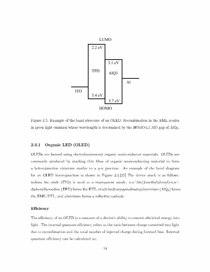
a heterojunction structure similar to a p-n junction. An example of the band diagram
for an OLED heterojunction is shown in Figure 2.5.[37] The device stack is as follows:
indium tin oxide (ITO) is used as a transparent anode, n,n´-bis(3-methylphenyl)-n,n´-
diphenylbenzidine (TPD) forms the HTL, tris(8-hydroxyquinolinato)aluminium (AlQ3) forms
the EML/ETL, and aluminum forms a re�ective cathode.
E�ciency
The e�ciency of an OLED is a measure of a device's ability to convert electrical energy into
light. The internal quantum e�ciency refers to the ratio between charge converted into light
due to recombination and the total number of injected charge during forward bias. Internal
quantum e�ciency can be calculated as:
14

ηint = γζsq
γ is the charge carrier balance. ζs is the exciton generation e�cency, i.e. the e�ciency
for exciting charge carriers into singlet (for �uorescence and phosphorescence) and triplet
(for phosphorescence only) excited states. q is the �uorescence quantum e�ciency, or the
e�ciency of generating photons from excited singlet or triplet states depending on whether
the OLED is �uorescent or phosphorescent.[38]
Singlet and triplet states refers to the excited charge states that occur according to the
pauli exclusion principle, where no two electrons occupying the same orbital can have the
same magnetic spin state. In the ground state, two electrons occupying the same orbital
must have opposite spins from each other. This con�guration is called the singlet ground
state (Figure 2.6). When light is absorbed by one of the electrons, they are excited to an
orbital with higher energy. If the spin state of the excited electron is preserved during the
transition, it is in a singlet excited state. If the spin state has been reversed and the spins of
both the unexcited electron and the excited electron are now aligned in parallel, it is called a
triplet state. Singlet-to-triplet and triplet-to-singlet transitions are typically far less likely to
occur due to the need for a spin transition on top of the usual energy absorption. Fluorescent
OLEDs are only able to produce light emission by singlet to singlet-state-transitions. Excited
singlet states can relax to triplet excited states by intersystem crossing, but these transitions
tend to have longer relaxation times and don't result in radiative emission for �uorescent
OLEDs. Thus, the theoretical maximum e�ciency for a �uorescent OLED is 25% since light
emission only occurs via 1 out of 4 available excited states (1 singlet excited state and 3
triplet excited states).[38] Phosphorescent OLEDs tend to include heavy metal structures
which allow for photon emission by both triplet-to-singlet relaxation and singlet-to-singlet
relaxation. Therefore, phosphorescent OLEDs have a theoretical maximum e�ciency of
100%.[38, 39, 40]
15
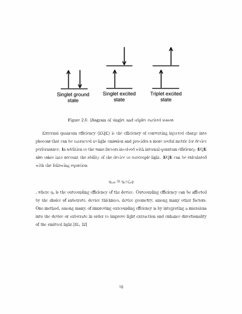
Figure 2.6: Diagram of singlet and triplet excited states.
External quantum e�ciency (EQE) is the e�ciency of converting injected charge into
photons that can be extracted as light emission and provides a more useful metric for device
performance. In addition to the same factors involved with internal quantum e�ciency, EQE
also takes into account the ability of the device to outcouple light. EQE can be calculated
with the following equation:
ηext ∼= ηoγζsq
, where ηo is the outcoupling e�ciency of the device. Outcoupling e�ciency can be a�ected
by the choice of substrate, device thickness, device geometry, among many other factors.
One method, among many, of improving outcoupling e�ciency is by integrating a microlens
into the device or substrate in order to improve light extraction and enhance directionality
of the emitted light.[41, 42]
16
Pathways of Degradation
A chief concern with the use of OLEDs is the relatively short operational lifetimes. The
organic materials and electrodes used are vulnerable to oxidation and moisture-related degra-
dation when exposed to atmospheric conditions. For this reason, OLEDs are typically fab-
ricated and assembled in inert environments, such as nitrogen or argon �lled gloveboxes.
Lifetime of OLED devices are usually quanti�ed by measuring the luminance over time,
during constant operation. One standard metric for the lifetime is the luminance half-life,
or the time it takes for an OLED's luminance to decay to half of its initial value.
Environmentally caused degradation to the device often manifests in dark spots,[43]
which decrease their luminance. Dark spot generation can be caused by local oxidation
of the cathodes, microscopic shorting between the electrodes due to localized heating and
morphological defects, charge accumulation at layer interfaces, and other structural defects
or damage.[44, 45, 38, 46] Lifetime can be improved by simply improving the e�ciency of the
device, reducing the thermal and electrical stress placed on the OLED.[46, 43] Furthermore,
environmental factors on device lifetime can be mitigated by using encapsulation or hermetic
sealing, providing a barrier against harmful oxygen and moisture.[44, 47] For �exible OLED
applications, �exible encapsulation schemes can also involve alternating stacks of deposited
thin barrier �lms.[48, 49, 50]
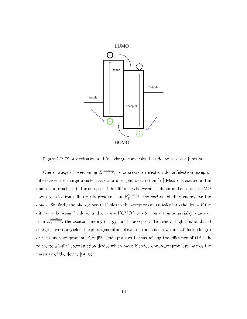
2.3.2 Organic Photodetector (OPD)
Organic photodiodes (OPDs) and organic solar cells operate similarly to their silicon coun-
terparts. Instead of n-type and p-type semiconductors, the photosensitive materials that
form the junction in OPDs are called electron acceptors and electron donors. When light
is absorbed by charge carriers in organic materials, an exciton (bound electron-hole pair)
with binding energy, Ebinding, is formed, rather than free charge carriers as with inorganic
photodetectors.[51] In order to generate photocurrent, the exciton binding energy must be
overcome to convert the exciton into free charge, and monolayers of organic photosensitive
material have poor e�ciencies since the excitons are not easily converted to free charge and
collected.[52, 51]
17
LUMO
HOMO
+
-
+
-Donor
Acceptor
Anode
Cathode
Figure 2.7: Photoexcitation and free charge conversion in a donor-acceptor junction.
One strategy of overcoming Ebinding, is to create an electron donor/electron acceptor
interface where charge transfer can occur after photoexcitation.[51] Electrons excited in the
donor can transfer into the acceptor if the di�erence between the donor and acceptor LUMO
levels (or electron a�nities) is greater than EbindingD , the exciton binding energy for the
donor. Similarly the photogenerated holes in the acceptor can transfer into the donor if the
di�erence between the donor and acceptor HOMO levels (or ionization potentials) is greater
than EbindingA , the exciton binding energy for the acceptor. To achieve high photoinduced
charge separation yields, the photogeneration of excitons must occur within a di�usion length
of the donor-acceptor interface.[53] One approach to maximizing the e�ciency of OPDs is
to create a bulk heterojunction device which has a blended donor-acceptor layer across the
majority of the device.[54, 55]
18
Responsivity and E�ciency
The internal quantum e�ciency of the OPD device is the ratio of charge carriers collected
at the contacts to the number of absorbed photons, whereas the external quantum e�ciency
(EQE) is the ratio of charge carriers collected at the contacts to the total number of incident
photons on the OPD's active area. EQE is mainly determined by the e�ciencies of the
free charge generation and the absorption cross section of the device. Responsivity, or the
extracted photocurrent divided by the incident light power, is related to EQE by :
R = EQE ∗ λqhc
, where λ is the wavelength of incident light, c is the speed of light, h is planck's constant,
and q is the electron charge. Responsivity is the primary metric for determining the practical
e�ectiveness of an OPD for implantable ORIS sensors.
2.3.3 Fabrication Methods
OLEDs and OPDs are typically fabricated by either physical vapor deposition under high
vacuum or by solution processing. While solution processing is appealing for applications like
roll-to-roll processing and large area fabrication, it is typically more challenging than vacuum
deposition since many organic materials are sensitive to solvents and high temperatures,
and vacuum deposited OLEDs have traditionally had higher performance.[56] With those
considerations, OLED and OPD stacks deposited by thermal evaporation under high vacuum
tend to be patterned by shadow masking. With shadow masking, a hard stencil is used
to cover areas where deposition of the evaporated material in question is not desired. One
downside of vacuum deposition of organic device layers is the relatively long processing times
related to placing the devices in high vacuum for deposition and frequent mask exchange
for sophisticated heterojunctions.
19
2.3.4 Biomedical Applications for OLED and OPD
Examples of OLED and OPD technology used in biomedical applications follows. These ex-
amples use a variety of fabrication methods and detection schemes, displaying the versatility
of OLED and OPD technologies applied to biosensors.
Organic Pulse Oximeter
Pulse oximetry is a noninvasive technique for optically measuring pulse and oxygenation
of blood through the skin. Typically, an emitter and photodetector pair are attached to a
body part, such as a �ngertip or earlobe. Light at two wavelengths is transmitted through
the body part and changes in light absorbance are recorded by the photodetector. Changes
in the absorbance of the two wavelengths correspond to changes in oxygenated and deoxy-
genated hemoglobin, providing a measure of the current ratio of the two. An alternative
technique measures changes in re�ected light from the surface of the body to achieve the
same diagnostic measurement.
An organic-based pulse oximeter was demonstrated by Lochner, et al. which replaced the
inorganic LED and photodetector elements with �exible OLEDs and OPDs. [57] The OLEDs
and OPD were fabricated using solution processing on a ITO-patterned glass substrate and
a polyethylene naphthalate (PEN) substrate, respectively, which could be wrapped around
a �nger for performing transmissive pulse oximetry measurements. To fabricate this device,
electrodes for the OLEDs and OPDs were formed by vacuum deposition. The active organic
layers for the OLEDs were spin-coated, including a TFB:F8BT:TBT emissive layer for the
red OLED and a TFB:F8BT emissive layer for the green OLED. The active layers for the
OPD were blade coated, including a PTB7:PC71BM photosensitive layer. A schematic of the
completed device and extracted pulse and oxygenation measurements are shown in Figure
2.8.
The solution processing techniques used to fabricate the device shows the potential for
low cost, large area production of organics based wearable biosensors. Additionally, the
ability to fabricate onto �exible substrates enables applications requiring the placement of
the sensors on di�erent areas of the body.
20
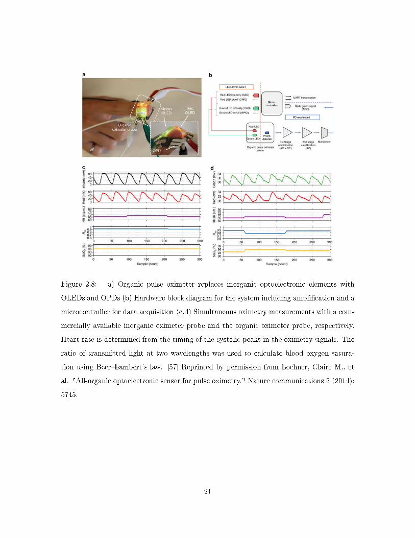
Figure 2.8: a) Organic pulse oximeter replaces inorganic optoelectronic elements with
OLEDs and OPDs (b) Hardware block diagram for the system including ampli�cation and a
microcontroller for data acquisition (c,d) Simultaneous oximetry measurements with a com-
mercially available inorganic oximeter probe and the organic oximeter probe, respectively.
Heart rate is determined from the timing of the systolic peaks in the oximetry signals. The
ratio of transmitted light at two wavelengths was used to calculate blood oxygen satura-
tion using Beer�Lambert's law. [57] Reprinted by permission from Lochner, Claire M., et
al. "All-organic optoelectronic sensor for pulse oximetry." Nature communications 5 (2014):
5745.
21
Miniature Laboratory-On-A-Chip Biosensor
Laboratory-on-a-chip (LOC) technologies which integrate sensors and devices onto an inte-
grated circuit (IC) capable of performing complete laboratory measurements and functions
are a potential solution for providing next generation point-of-care diagnostics requiring a
compact physical footprint, portability, and ease of operation/automation. Wojciechowski,
et al. demonstrated a micro�uidic LOC biosensor with an integrated OPD for performing
chemiluminescence (CL) detection of a toxin, Staphylococcal enterotoxin B (SEB). [58] CL
detectors record light emissions from chemical reactions that lead to photoexcitation and
are used for immunoassays and nucleic acid detection. [59] These detectors do not require
a light source as only a photodetector is needed to measure the photoemission from the
chemical reactions, decreasing the footprint and complexity of the devices.
Figure 2.9: Miniaturized biosensor using OPDs. [58] a) A glass slide with a printed OPD
sensor is used for CL detection of SEB b) The glass slide is placed into a portable con-
troller for data acquisition. Reprinted with permission from Wojciechowski, Jason R., et
al. "Organic photodiodes for biosensor miniaturization." Analytical chemistry 81.9 (2009):
3455-3461. Copyright 2009 American Chemical Society."
22
The OPD based CL detector, shown in Figure 2.9, consisted of an OPD printed onto a
glass slide with an active area of 4 x 4 mm and a quantum e�ciency of 50-60% at the 532 nm
wavelength. A sandwich immunoassay was performed directly onto the OPD slide, where
the slide was coated with α-SEB capture antibody, then exposed to SEB, and incubated
with horseradish peroxidase (HRP)-conjugated α-SEB tracer antibody (α-SEB-HRP) . An
opaque micro�uidic chamber was attached to the sensor, and the slide was placed into a
portable OPD controller for data acquisition.
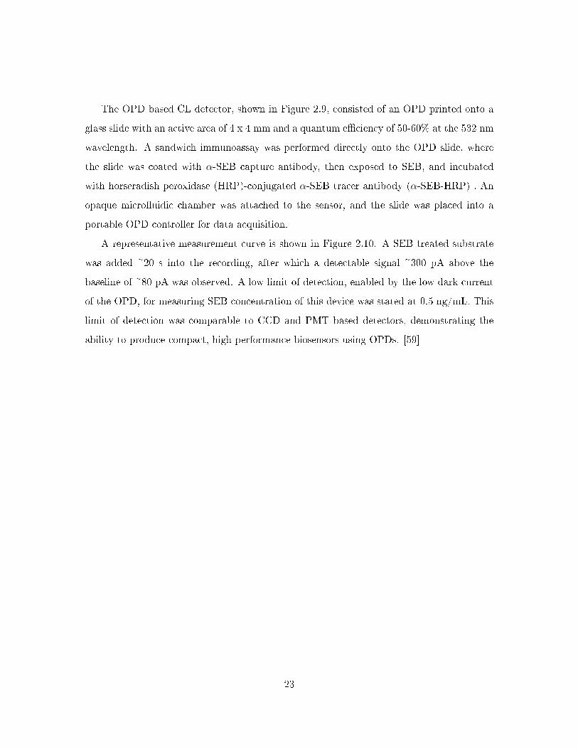
A representative measurement curve is shown in Figure 2.10. A SEB treated substrate
was added ~20 s into the recording, after which a detectable signal ~300 pA above the
baseline of ~80 pA was observed. A low limit of detection, enabled by the low dark current
of the OPD, for measuring SEB concentration of this device was stated at 0.5 ng/mL. This
limit of detection was comparable to CCD and PMT based detectors, demonstrating the
ability to produce compact, high performance biosensors using OPDs. [59]
23
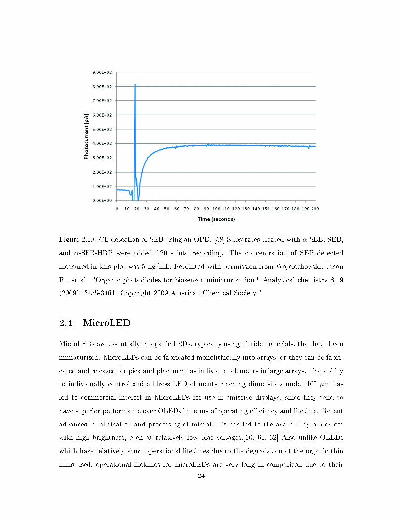
Figure 2.10: CL detection of SEB using an OPD. [58] Substrates treated with α-SEB, SEB,
and α-SEB-HRP were added ~20 s into recording. The concentration of SEB detected
measured in this plot was 5 ng/mL. Reprinted with permission from Wojciechowski, Jason
R., et al. "Organic photodiodes for biosensor miniaturization." Analytical chemistry 81.9
(2009): 3455-3461. Copyright 2009 American Chemical Society."
2.4 MicroLED
MicroLEDs are essentially inorganic LEDs, typically using nitride materials, that have been
miniaturized. MicroLEDs can be fabricated monolithically into arrays, or they can be fabri-
cated and released for pick and placement as individual elements in large arrays. The ability
to individually control and address LED elements reaching dimensions under 100 µm has
led to commercial interest in MicroLEDs for use in emissive displays, since they tend to
have superior performance over OLEDs in terms of operating e�ciency and lifetime. Recent
advances in fabrication and processing of microLEDs has led to the availability of devices
with high brightness, even at relatively low bias voltages.[60, 61, 62] Also unlike OLEDs
which have relatively short operational lifetimes due to the degradation of the organic thin
�lms used, operational lifetimes for microLEDs are very long in comparison due to their
24
inorganic composition. While these advantages in performance are ideal for use in long-
term in vivo measurement of ORIS, the drawback of microLEDs is their intrinsic rigidity.
Embedding microLEDs in a �exible circuit or substrate ultimately limits the �exibility of
the �nal device. Additionally, the planar geometry of most microLED elements can lead to
structurally vulnerabilities when used in a �exible device architecture; however, this can be
overcome with appropriate strain engineering. [63]
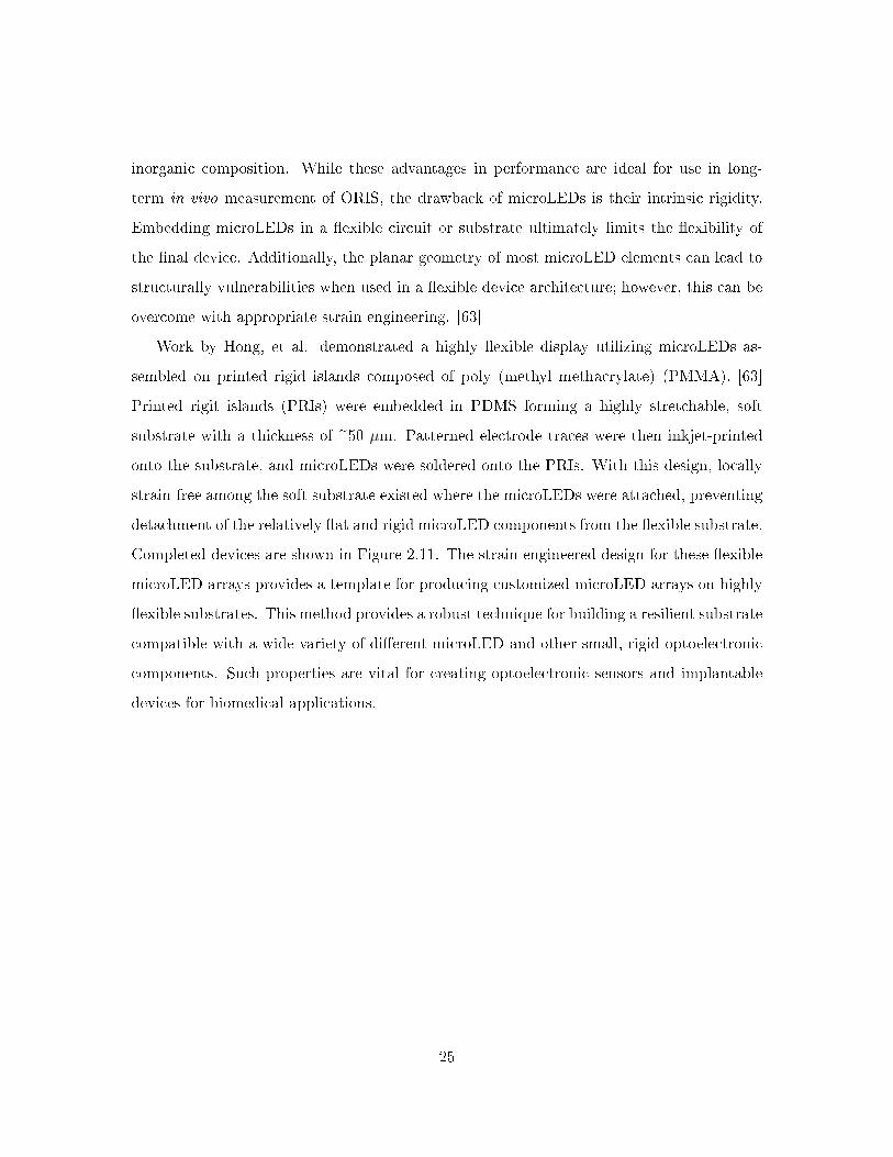
Work by Hong, et al. demonstrated a highly �exible display utilizing microLEDs as-
sembled on printed rigid islands composed of poly (methyl methacrylate) (PMMA). [63]
Printed rigit islands (PRIs) were embedded in PDMS forming a highly stretchable, soft
substrate with a thickness of ~50 µm. Patterned electrode traces were then inkjet-printed
onto the substrate, and microLEDs were soldered onto the PRIs. With this design, locally
strain-free among the soft substrate existed where the microLEDs were attached, preventing
detachment of the relatively �at and rigid microLED components from the �exible substrate.
Completed devices are shown in Figure 2.11. The strain engineered design for these �exible
microLED arrays provides a template for producing customized microLED arrays on highly
�exible substrates. This method provides a robust technique for building a resilient substrate
compatible with a wide variety of di�erent microLED and other small, rigid optoelectronic
components. Such properties are vital for creating optoelectronic sensors and implantable
devices for biomedical applications.
25
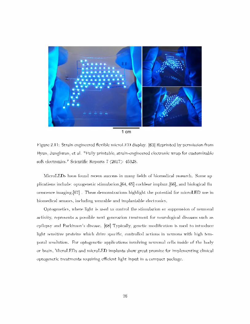
Figure 2.11: Strain engineered �exible microLED display. [63] Reprinted by permission from
Byun, Junghwan, et al. "Fully printable, strain-engineered electronic wrap for customizable
soft electronics." Scienti�c Reports 7 (2017): 45328.
MicroLEDs have found recent success in many �elds of biomedical research. Some ap-
plications include: optogenetic stimulation,[64, 65] cochlear implant,[66], and biological �u-
orescence imaging.[67] . These demonstrations highlight the potential for microLED use in
biomedical sensors, including wearable and implantable electronics.
Optogenetics, where light is used to control the stimulation or suppression of neuronal
activity, represents a possible next generation treatment for neurological diseases such as
epilepsy and Parkinson's disease. [68] Typically, genetic modi�cation is used to introduce
light sensitive proteins which drive speci�c, controlled actions in neurons with high tem-
poral resolution. For optogenetic applications involving neuronal cells inside of the body
or brain, MicroLEDs and microLED implants show great promise for implementing clinical
optogenetic treatments requiring e�cient light input in a compact package.
26
One successful application of microLEDs in this �eld was accomplished by Montgomery,
et. al where a microLED implanted on the surface of a mouse's brain was operated com-
pletely wirelessly for optogenetic stimulation. [65] In this work, a commercial blue microLED
was attached to a circuit for wireless power delivery. A mouse expressing channelrhodopsin
2 (ChR2) was implanted with the device and placed above a resonant cavity for RF wireless
power delivery (Figure 2.12). When the microLED was powered on, the blue light emission
activates ChR2 , triggering a circling behavior in the mouse's movement. The setup was
able to produce enough light input (1-20 mW/mm2) for ChR2 activation without exces-
sive heating of the animal (< 1 C change in body temperature) by duty cycling under 40%.
This achievement represents one practical approach to advanced healthcare for patients with
neurological diseases utilizing implantable optoelectronic devices.
MicroLEDs used for ORIS measurements in this work are commercially available and
are packaged as individual elements. The microLEDs have preformed AuSn solder bumps
for eutectic die attach. This allows the chips to be placed on a substrate or circuit with
a die bonder or via �ip chip bonding, without the need for wire bonding or traditional
soldering. Because of the thermal processing required to re�ow the AuSn solder, substrates
and materials that can withstand relatively high temperatures must be used. Additionally,
the small footprint of the bond pads calls for the use of photolithographically patterned
circuitry and bond sites, meaning the substrates used must be resistant to solvents and UV
light exposure. This limits the available substrates and materials for use in �exible and
implantable devices integdvanced healthcare for patients with neurological diseases utilizing
implantablerated with microLEDs.
27

Figure 2.12: Wireless optogenetic stimulation of mice using a microLED implant a) A mouse
implanted with the wireless blue microLED implant was con�ned to an enclosure containing
a resonant cavity for wireless power delivery. The blue microLED was powered on wirelessly,
triggering a circulatory motor behavior induced by the activation of ChR2 b) Schematic of
the wireless microLED implant c) Photograph of the microLED implant [65] Reprinted by
permission fromMontgomery, Kate L., et al. "Wirelessly powered, fully internal optogenetics
for brain, spinal and peripheral circuits in mice." Nature methods 12.10 (2015): 969-974.
28
2.5 Colloidal Quantum Dots
Colloidal quantum dots (QDs) are nanocrystals of semiconducting material produced by
solution processing that exhibit quantum e�ects due to their small size. The optoelectronic
properties of QDs are a function of their size and structure.[69, 70] Electrons in QDs be-
have much like �particles in a box� with quantum con�nement e�ects in 3 dimensions.[70]
The discrete electronic states that arise from con�nement result in very sharp spectral qual-
ities. As such, QDs have been adopted in many commercial displays and are being thor-
oughly researched for their potential applications in optoelectronnics [71, 72, 73] and imaging
biomarkers[74, 75, 76]. In particular the wavelength of emitted light can be tightly tuned
with narrow spectra by adjusting their size and structure, but without changing the mate-
rial composition.[73] This is a huge advantage over other optoelectronic devices which tend
to have less tunable emission spectra heavily dependent on the material composition. The
synthesis of QDs is discussed in the appendix.
2.5.1 Electroluminescent QDLEDs vs. Photoluminescent QDs
There are two variants of LED technology that takes advantage of QDs. The �rst is the
electroluminescent quantum dot LED (QDLED), which operates similarly to an OLED.
QDLEDs are comprised of a thin layer, often just a single monolayer, of QDs sandwiched
between charge transport layers. Excitons in QDLED can occur by either photon charge
injection, energy transfer, or by ionization of QDs.[73] The relaxation of these QD excitons
results in electroluminescence at photon energies equal to the bandgap of the QD. The
primary di�erence between di�erent kinds of QDLEDs reside in the charge transport layers,
which may be formed with organic, inorganic, or a hybrid mixture of organic and inorganic
materials.[73, 71, 72]
Photoluminescent QDs di�er from QDLEDs in that they are optically driven, rather
than electronically driven. This is most commonly seen in displays where white or blue
backlight is converted by a QD dye by absorption and re-emission.[77] Adopting QDs into
other optoelectronic devices can enhance them by providing a level of wavelength tunability
that is not normally available. This versatility is crucial in optimizing the performance of
29
implantable and wearable optoelectronic sensors and expanding their practical applications.
2.5.2 Biomedical Applications for Quantum Dots
Examples of the use of QDs in biomedical applications follows. These examples take ad-
vantage of the unique optical properties of QDs for providing highly tunable narrowband
light emission. The progress reported in these examples show the promise of future clinical
therapies which utilize advanced materials such as QDs.
Photodynamic Therapy
Photodynamic therapies involve activating photosensitizers with speci�c wavelengths of light
to destroy cancer cells, for example via reactive oxygen species (ROS). [78] Therapies in-
volving external illumination for targeting cancer cells within the body are limited by the
penetration depth of the light and may have undesired side e�ects due to photosensitivity of
the skin. The use of nanotechnology to reduce or eliminate the required external irradiation
has been a topic of interest in the development of photodynamic therapies.
Work by Hsu et al. demonstrated the use of QDs in targeted photodynamic therapy re-
quiring zero external irradiation (Figure 2.13). [79] The QD-conjugate used in this work were
composed of light-emitting Renilla luciferase 8 (RLuc8) proteins and carboxylate-containing
QDs, which self illuminate via bioluminescent resonant energy transfer (BRET).[80] In the
BRET process, energy is released from the RLuc8 substrate coelenterazine, electronically
exciting the QD which than emit light. BRET was used to internally illuminate meta-tetra-
hydroxyphenyl-chlorin (m-THPC) photosensitizers in photodynamic therapy targeting the
reduction of tumors (Figure 2.13).
30
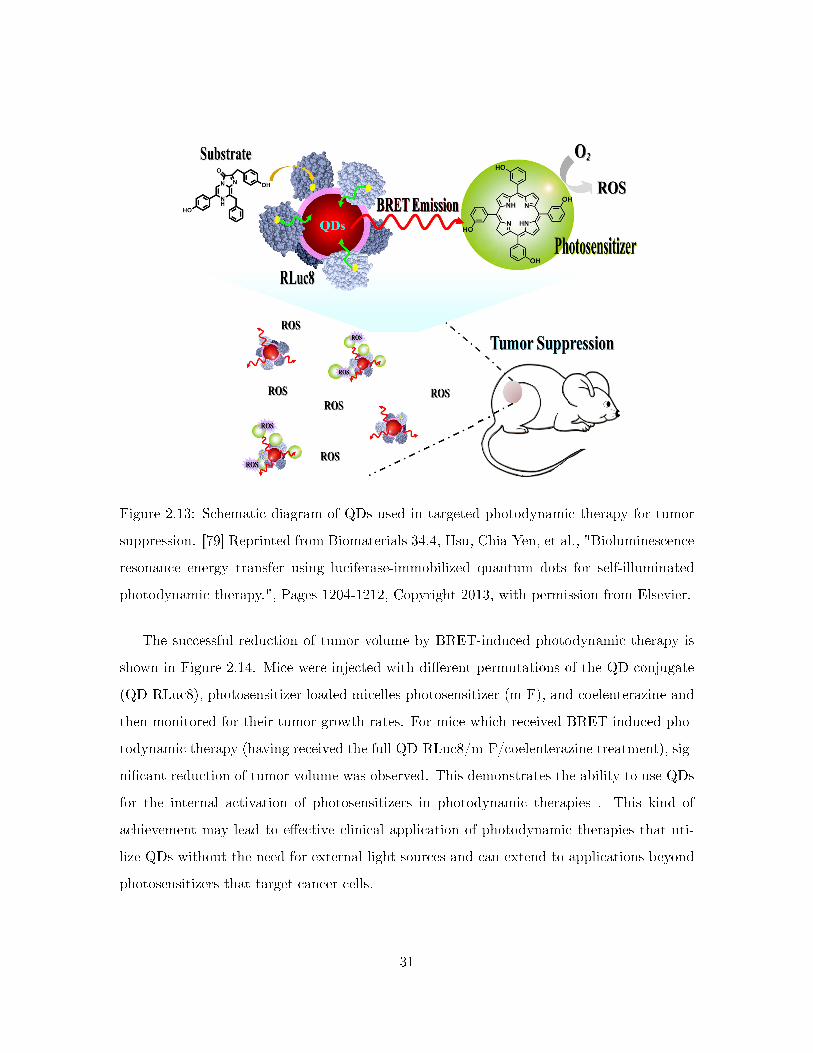
Figure 2.13: Schematic diagram of QDs used in targeted photodynamic therapy for tumor
suppression. [79] Reprinted from Biomaterials 34.4, Hsu, Chia-Yen, et al., "Bioluminescence
resonance energy transfer using luciferase-immobilized quantum dots for self-illuminated
photodynamic therapy.", Pages 1204-1212, Copyright 2013, with permission from Elsevier.
The successful reduction of tumor volume by BRET-induced photodynamic therapy is
shown in Figure 2.14. Mice were injected with di�erent permutations of the QD-conjugate
(QD-RLuc8), photosensitizer loaded micelles photosensitizer (m-F), and coelenterazine and
then monitored for their tumor growth rates. For mice which received BRET-induced pho-
todynamic therapy (having received the full QD-RLuc8/m-F/coelenterazine treatment), sig-
ni�cant reduction of tumor volume was observed. This demonstrates the ability to use QDs
for the internal activation of photosensitizers in photodynamic therapies . This kind of
achievement may lead to e�ective clinical application of photodynamic therapies that uti-
lize QDs without the need for external light sources and can extend to applications beyond
photosensitizers that target cancer cells.
31
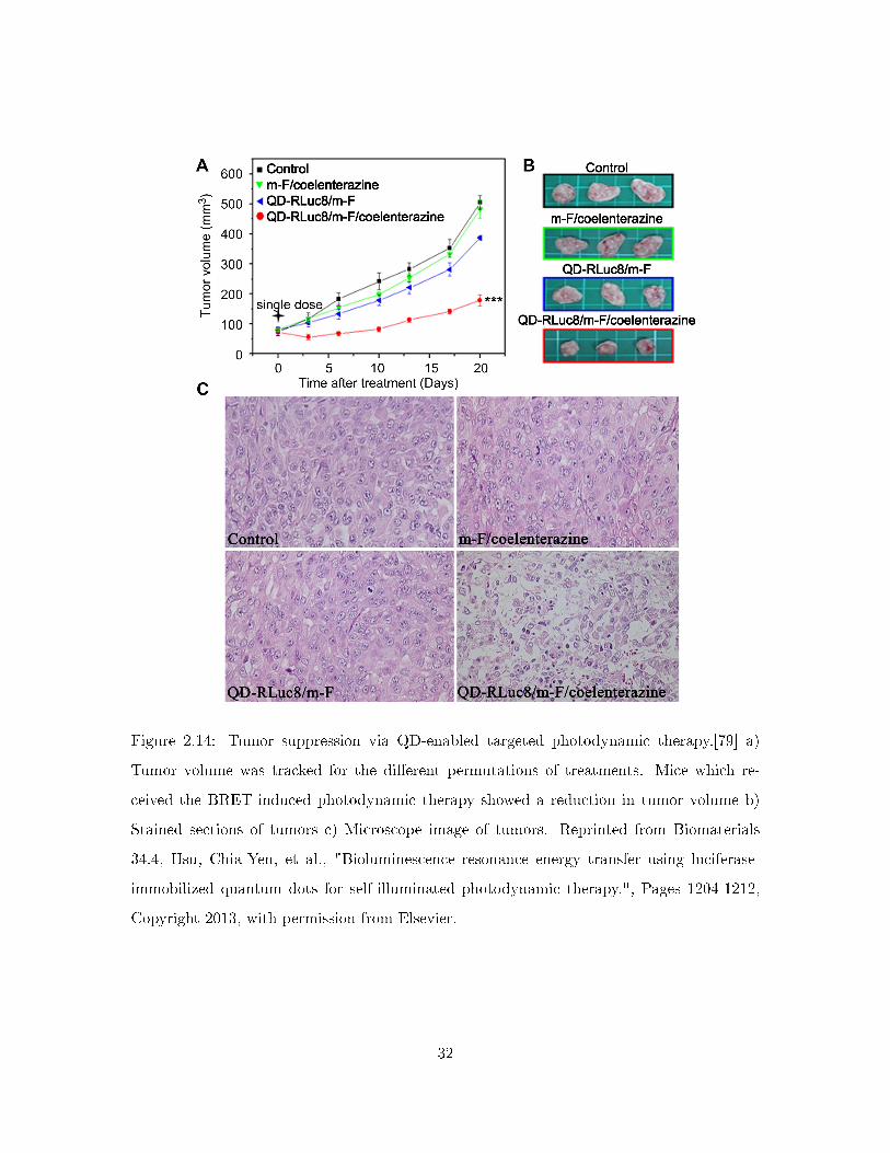
Figure 2.14: Tumor suppression via QD-enabled targeted photodynamic therapy.[79] a)
Tumor volume was tracked for the di�erent permutations of treatments. Mice which re-
ceived the BRET-induced photodynamic therapy showed a reduction in tumor volume b)
Stained sections of tumors c) Microscope image of tumors. Reprinted from Biomaterials
34.4, Hsu, Chia-Yen, et al., "Bioluminescence resonance energy transfer using luciferase-
immobilized quantum dots for self-illuminated photodynamic therapy.", Pages 1204-1212,
Copyright 2013, with permission from Elsevier.
32
QDLEDs for Photobiomodulation
The use of electroluminescent (EL) QDLEDs in wearable devices and biomedical devices
has gathered interest as QD technology has progressed both commercially and for research
purposes. Chen et al. demonstrated the use of EL QDLEDs for photobiomodulation, in
which light is used to stimulate cellular function. [81] Such treatments could potentially
aid with wound recovery via applications such as light emitting bandages. In their work,
QDLEDs which have brighter emissions at the necessary wavelengths (in the deep red region)
were proposed as an alternative to OLEDs which have struggled to meet the performance
requirements for such applications. The performance and structure of such QDLEDs is
shown in Figure 2.15.
These highly e�cient QDLEDs produced high brightness emission, up to 165,000 Cd/m2
at a peak emission wavelength of 620 nm.[81] In-vitro studies of these QDLEDs used in
photobiomodulation therapy were performed using cell lines (HEp-2 [ATCC-CCL-2]; L929
[ATCC-CCL-1], 3T3 [ATCC-CRC-2593]) which act as surrogates for whole animal studies
of wound healing. The QDLEDs were placed underneath cell culture wells containing the
cell lines, and the QDLEDs were powered on for 10 min, illuminating the cell lines for
photobiomodulation therapy (Figure 2.16). Assay results at 24 hours post treatment showed
increased cell metabolism comparable to previous results achieved with inorganic LEDs
(up to 27.9% increase for the HEp-2 cell line). [81] While improvements in performance
for �exible QDLEDs of this type must be made in order to enable applications such as
wearable or bandage based photobiomodulation treatments, the devices demonstrated in
this work show the potential for utilizing the unique optical properties of QDs in wearable
and implantable applications.
33
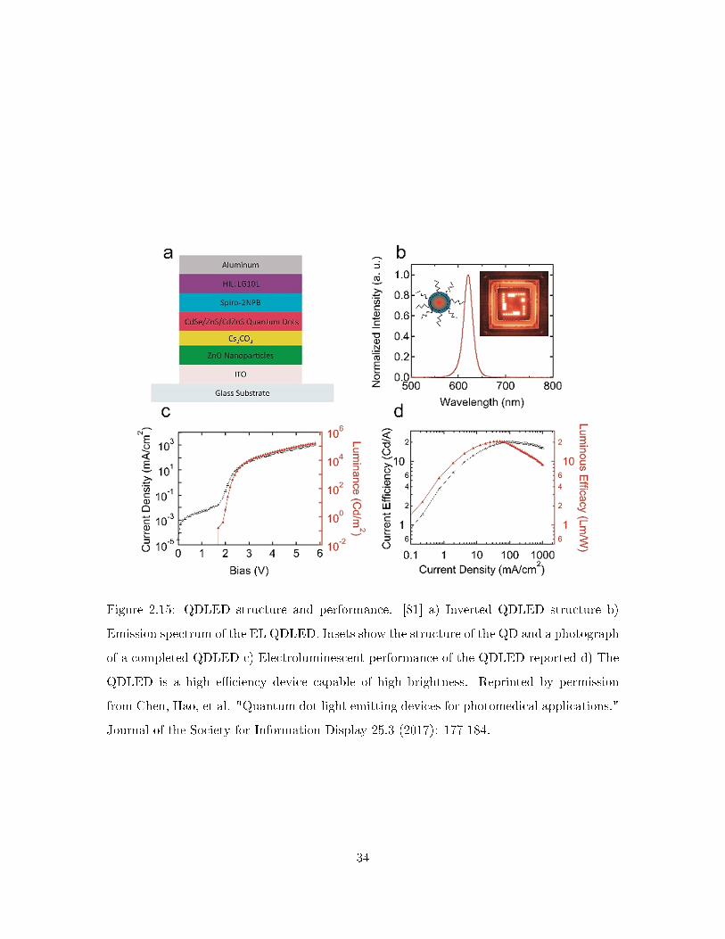
Figure 2.15: QDLED structure and performance. [81] a) Inverted QDLED structure b)
Emission spectrum of the EL QDLED. Insets show the structure of the QD and a photograph
of a completed QDLED c) Electroluminescent performance of the QDLED reported d) The
QDLED is a high e�ciency device capable of high brightness. Reprinted by permission
from Chen, Hao, et al. "Quantum dot light emitting devices for photomedical applications."
Journal of the Society for Information Display 25.3 (2017): 177-184.
34
Figure 2.16: Photograph and schematic of the QDLED photobiomodulation therapy. [81]
a) Photograph of the red QDLED with 620 nm peak emission b) The QDLED is placed un-
derneath the transparent cell culture wells to perform in-vitro photobiomodulation therapy
c) Schematic of the control experiment with no illumination d) Schematic of the cell lines
receiving photobiomodulation therapy using a QDLED. Reprinted by permission from Chen,
Hao, et al. "Quantum dot light emitting devices for photomedical applications." Journal of
the Society for Information Display 25.3 (2017): 177-184.
35
Chapter 3
Integrated Organic LED and Organic
Photodetector on a Highly Flexible
Parylene-C Substrate
3.1 Highly �exible substrate
In order to achieve high levels of �exibility, a polymer based substrate was used. Biocompat-
ible plastic substrates such as poly(ethylene 2,6-naphthalate) and poly(ethyl benzene-1,4-
dicarboxylate), or PEN and PET respectively, are commonly used for �exible displays using
OLEDs. However, the bending radius for these substrates are typically limited to around
5 mm.[82, 2] In order to achieve higher �exibility and conformal attachment, free-standing
parylene-c is used as the substrate and encapsulation. Parylene (poly(p-xylylene)) is a poly-
mer, deposited by chemical vapor deposition, which is often used for barrier coatings and
biocompatible membranes/interfaces.[83] Parylene-c is the variant of the parylene polymer
which has one chlorine group per repeat unit (Figure 3.1). Conformal coatings of parylene-c
are chemically and electrically inert, biocompatible �lms,[84, 85] ideal for passivating the
devices and protecting them from the environment of the brain.
36
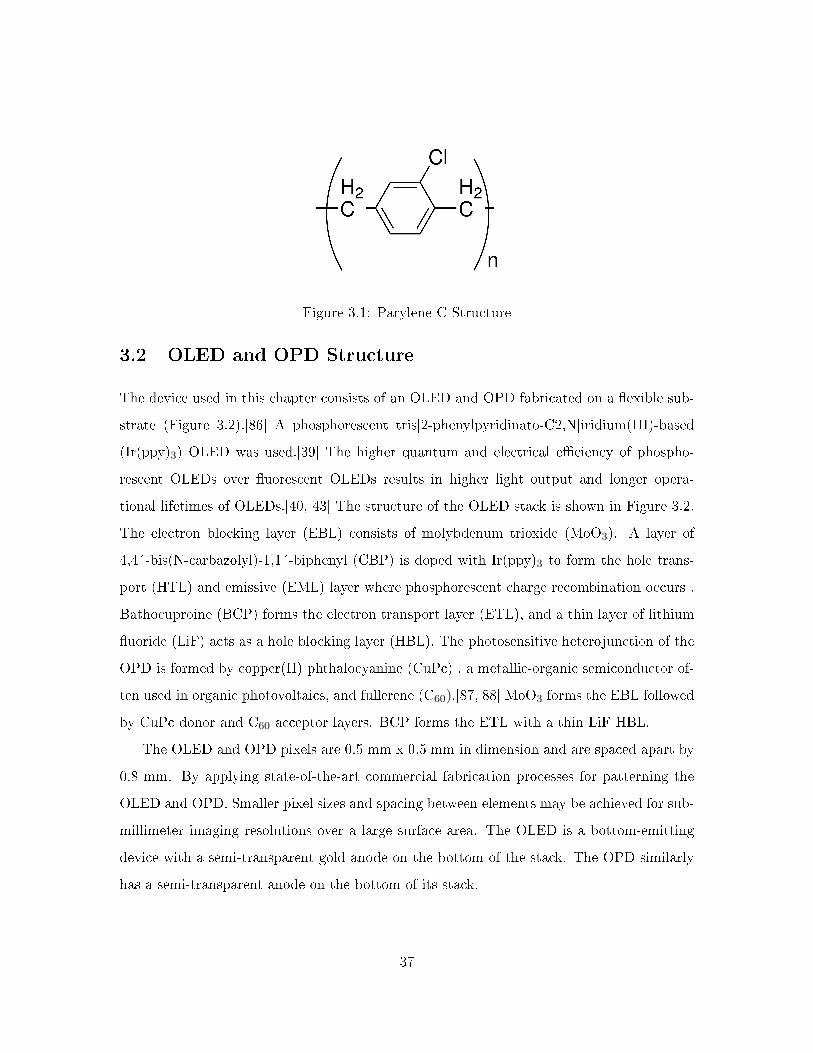
Figure 3.1: Parylene-C Structure
3.2 OLED and OPD Structure
The device used in this chapter consists of an OLED and OPD fabricated on a �exible sub-
strate (Figure 3.2).[86] A phosphorescent tris[2-phenylpyridinato-C2,N]iridium(III)-based
(Ir(ppy)3) OLED was used.[39] The higher quantum and electrical e�ciency of phospho-
rescent OLEDs over �uorescent OLEDs results in higher light output and longer opera-
tional lifetimes of OLEDs.[40, 43] The structure of the OLED stack is shown in Figure 3.2.
The electron blocking layer (EBL) consists of molybdenum trioxide (MoO3). A layer of
4,4´-bis(N-carbazolyl)-1,1´-biphenyl (CBP) is doped with Ir(ppy)3 to form the hole trans-
port (HTL) and emissive (EML) layer where phosphorescent charge recombination occurs .
Bathocuproine (BCP) forms the electron transport layer (ETL), and a thin layer of lithium
�uoride (LiF) acts as a hole blocking layer (HBL). The photosensitive heterojunction of the
OPD is formed by copper(II) phthalocyanine (CuPc) , a metallic-organic semiconductor of-
ten used in organic photovoltaics, and fullerene (C60).[87, 88] MoO3 forms the EBL followed
by CuPc donor and C60 acceptor layers. BCP forms the ETL with a thin LiF HBL.
The OLED and OPD pixels are 0.5 mm x 0.5 mm in dimension and are spaced apart by
0.8 mm. By applying state-of-the-art commercial fabrication processes for patterning the
OLED and OPD. Smaller pixel sizes and spacing between elements may be achieved for sub-
millimeter imaging resolutions over a large surface area. The OLED is a bottom-emitting
device with a semi-transparent gold anode on the bottom of the stack. The OPD similarly
has a semi-transparent anode on the bottom of its stack.
37
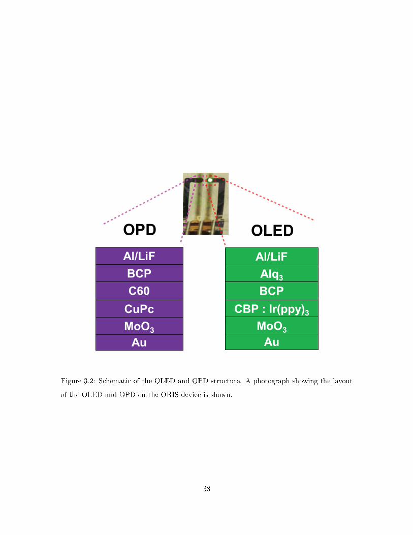
Al/LiF
BCP
CuPc
Au
C60
MoO3
Al/LiF
Alq3
CBP : Ir(ppy)3
Au
BCP
MoO3
OPD OLED
Figure 3.2: Schematic of the OLED and OPD structure. A photograph showing the layout
of the OLED and OPD on the ORIS device is shown.
38
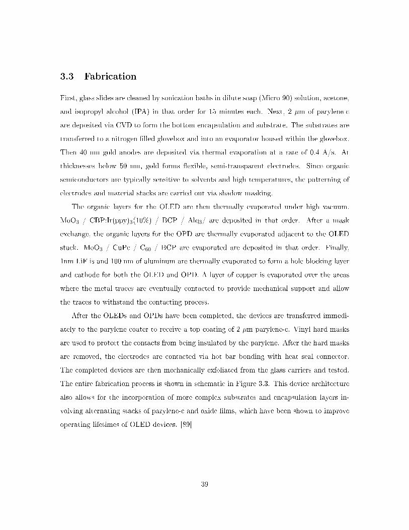
3.3 Fabrication
First, glass slides are cleaned by sonication baths in dilute soap (Micro-90) solution, acetone,
and isopropyl alcohol (IPA) in that order for 15 minutes each. Next, 2 µm of parylene-c
are deposited via CVD to form the bottom encapsulation and substrate. The substrates are
transferred to a nitrogen �lled glovebox and into an evaporator housed within the glovebox.
Then 40 nm gold anodes are deposited via thermal evaporation at a rate of 0.4 Å/s. At
thicknesses below 50 nm, gold forms �exible, semi-transparent electrodes. Since organic
semiconductors are typically sensitive to solvents and high temperatures, the patterning of
electrodes and material stacks are carried out via shadow masking.
The organic layers for the OLED are then thermally evaporated under high vacuum.
MoO3 / CBP:Ir(ppy)3(10%) / BCP / Alq3/ are deposited in that order. After a mask
exchange, the organic layers for the OPD are thermally evaporated adjacent to the OLED
stack. MoO3 / CuPc / C60 / BCP are evaporated are deposited in that order. Finally,
1nm LiF is and 100 nm of aluminum are thermally evaporated to form a hole blocking layer
and cathode for both the OLED and OPD. A layer of copper is evaporated over the areas
where the metal traces are eventually contacted to provide mechanical support and allow
the traces to withstand the contacting process.
After the OLEDs and OPDs have been completed, the devices are transferred immedi-
ately to the parylene coater to receive a top coating of 2 µm parylene-c. Vinyl hard masks
are used to protect the contacts from being insulated by the parylene. After the hard masks
are removed, the electrodes are contacted via hot bar bonding with heat seal connector.
The completed devices are then mechanically exfoliated from the glass carriers and tested.
The entire fabrication process is shown in schematic in Figure 3.3. This device architecture
also allows for the incorporation of more complex substrates and encapsulation layers in-
volving alternating stacks of parylene-c and oxide �lms, which have been shown to improve
operating lifetimes of OLED devices. [89]
39
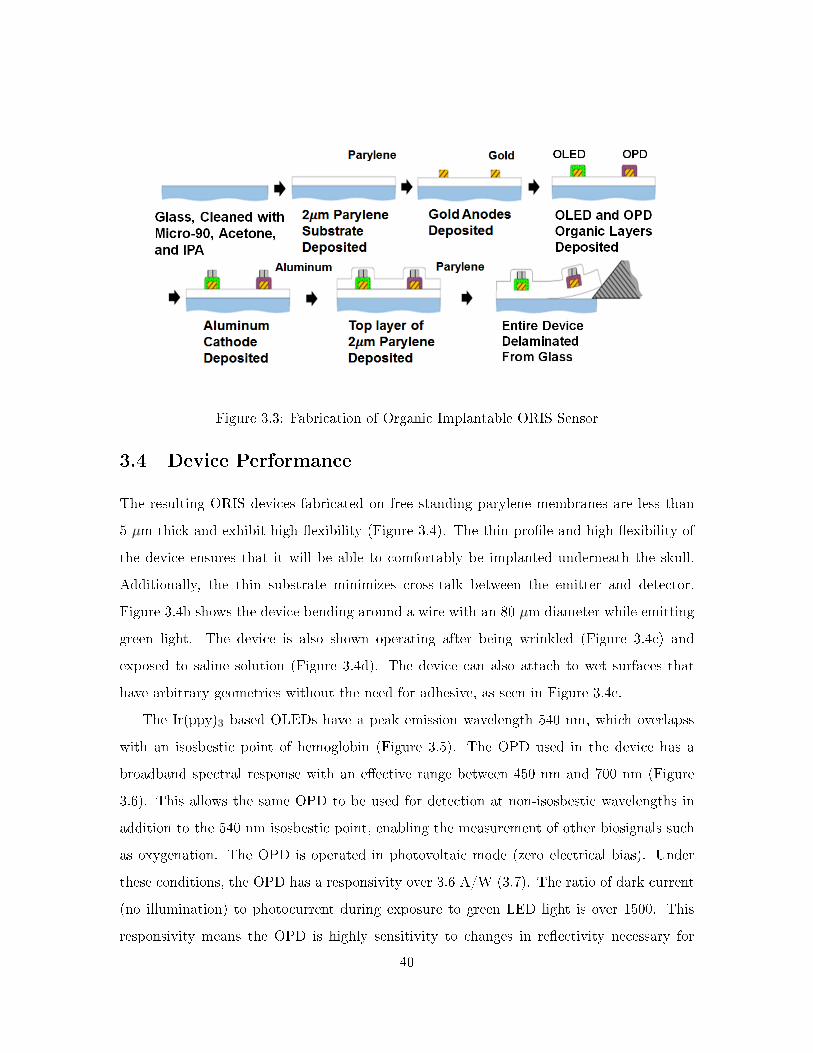
Figure 3.3: Fabrication of Organic Implantable ORIS Sensor
3.4 Device Performance
The resulting ORIS devices fabricated on free standing parylene membranes are less than
5 µm thick and exhibit high �exibility (Figure 3.4). The thin pro�le and high �exibility of
the device ensures that it will be able to comfortably be implanted underneath the skull.
Additionally, the thin substrate minimizes cross-talk between the emitter and detector.
Figure 3.4b shows the device bending around a wire with an 80 µm diameter while emitting
green light. The device is also shown operating after being wrinkled (Figure 3.4c) and
exposed to saline solution (Figure 3.4d). The device can also attach to wet surfaces that
have arbitrary geometries without the need for adhesive, as seen in Figure 3.4e.
The Ir(ppy)3 based OLEDs have a peak emission wavelength 540 nm, which overlapss
with an isosbestic point of hemoglobin (Figure 3.5). The OPD used in the device has a
broadband spectral response with an e�ective range between 450 nm and 700 nm (Figure
3.6). This allows the same OPD to be used for detection at non-isosbestic wavelengths in
addition to the 540 nm isosbestic point, enabling the measurement of other biosignals such
as oxygenation. The OPD is operated in photovoltaic mode (zero electrical bias). Under
these conditions, the OPD has a responsivity over 3.6 A/W (3.7). The ratio of dark current
(no illumination) to photocurrent during exposure to green LED light is over 1500. This
responsivity means the OPD is highly sensitivity to changes in re�ectivity necessary for
40
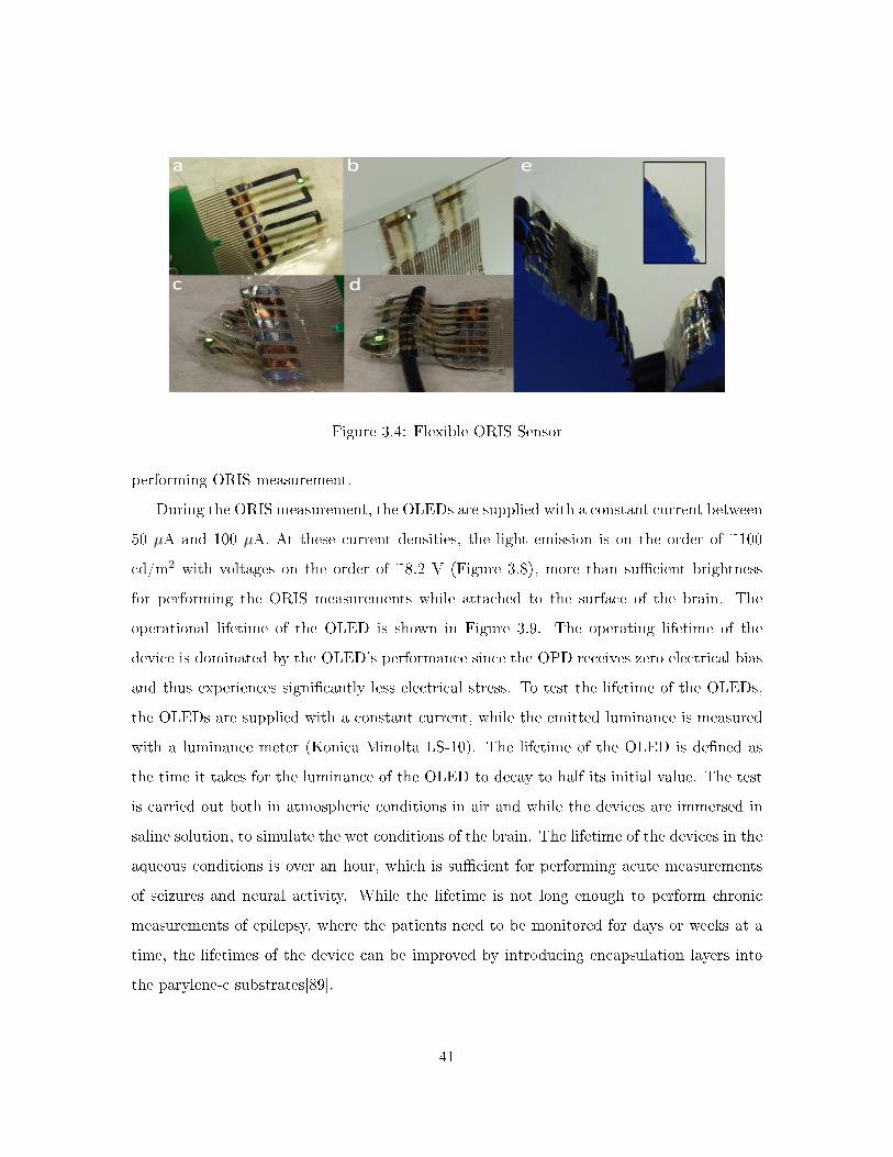
Figure 3.4: Flexible ORIS Sensor
performing ORIS measurement.
During the ORIS measurement, the OLEDs are supplied with a constant current between
50 µA and 100 µA. At these current densities, the light emission is on the order of ~100
cd/m2 with voltages on the order of ~8.2 V (Figure 3.8), more than su�cient brightness
for performing the ORIS measurements while attached to the surface of the brain. The
operational lifetime of the OLED is shown in Figure 3.9. The operating lifetime of the
device is dominated by the OLED's performance since the OPD receives zero electrical bias
and thus experiences signi�cantly less electrical stress. To test the lifetime of the OLEDs,
the OLEDs are supplied with a constant current, while the emitted luminance is measured
with a luminance meter (Konica Minolta LS-10). The lifetime of the OLED is de�ned as
the time it takes for the luminance of the OLED to decay to half its initial value. The test
is carried out both in atmospheric conditions in air and while the devices are immersed in
saline solution, to simulate the wet conditions of the brain. The lifetime of the devices in the
aqueous conditions is over an hour, which is su�cient for performing acute measurements
of seizures and neural activity. While the lifetime is not long enough to perform chronic
measurements of epilepsy, where the patients need to be monitored for days or weeks at a
time, the lifetimes of the device can be improved by introducing encapsulation layers into
the parylene-c substrates[89].
41
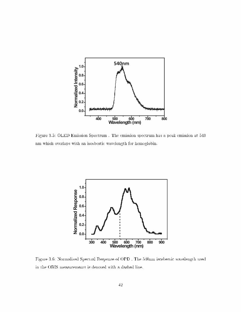
Figure 3.5: OLED Emission Spectrum . The emission spectrum has a peak emission at 540
nm which overlaps with an isosbestic wavelength for hemoglobin.
Figure 3.6: Normalized Spectral Response of OPD . The 540nm isosbestic wavelength used
in the ORIS measurements is denoted with a dashed line.
42
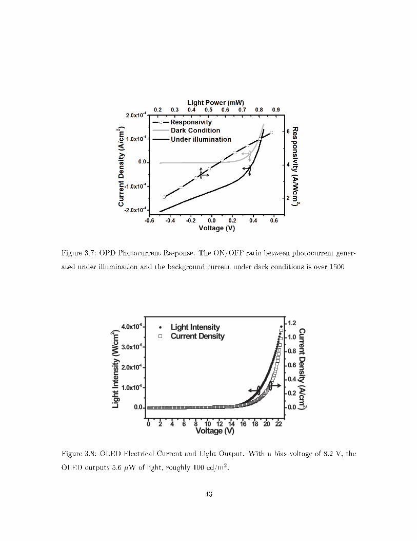
Figure 3.7: OPD Photocurrent Response. The ON/OFF ratio between photocurrent gener-
ated under illumination and the background current under dark conditions is over 1500
Figure 3.8: OLED Electrical Current and Light Output. With a bias voltage of 8.2 V, the
OLED outputs 5.6 µW of light, roughly 100 cd/m2.
43
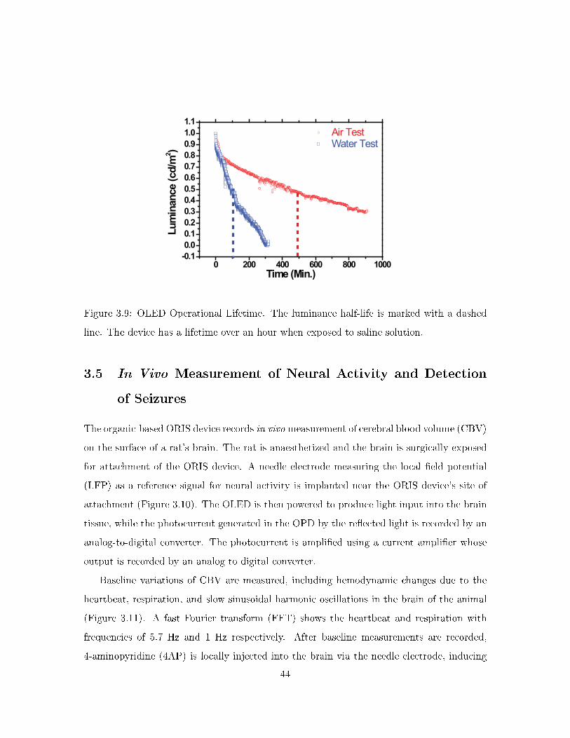
0 200 400 600 800 1000-0.1
0.0
0.1
0.2
0.3
0.4
0.5
0.6
0.7
0.8
0.9
1.0
1.1
Air Test
Water Test
Lum
inance (cd/m
2)
Time (Min.)
Figure 3.9: OLED Operational Lifetime. The luminance half-life is marked with a dashed
line. The device has a lifetime over an hour when exposed to saline solution.
3.5 In Vivo Measurement of Neural Activity and Detection
of Seizures
The organic-based ORIS device records in vivo measurement of cerebral blood volume (CBV)
on the surface of a rat's brain. The rat is anaesthetized and the brain is surgically exposed
for attachment of the ORIS device. A needle electrode measuring the local �eld potential
(LFP) as a reference signal for neural activity is implanted near the ORIS device's site of
attachment (Figure 3.10). The OLED is then powered to produce light input into the brain
tissue, while the photocurrent generated in the OPD by the re�ected light is recorded by an
analog-to-digital converter. The photocurrent is ampli�ed using a current ampli�er whose
output is recorded by an analog to digital converter.
Baseline variations of CBV are measured, including hemodynamic changes due to the
heartbeat, respiration, and slow sinusoidal harmonic oscillations in the brain of the animal
(Figure 3.11). A fast Fourier transform (FFT) shows the heartbeat and respiration with
frequencies of 5.7 Hz and 1 Hz respectively. After baseline measurements are recorded,
4-aminopyridine (4AP) is locally injected into the brain via the needle electrode, inducing
44
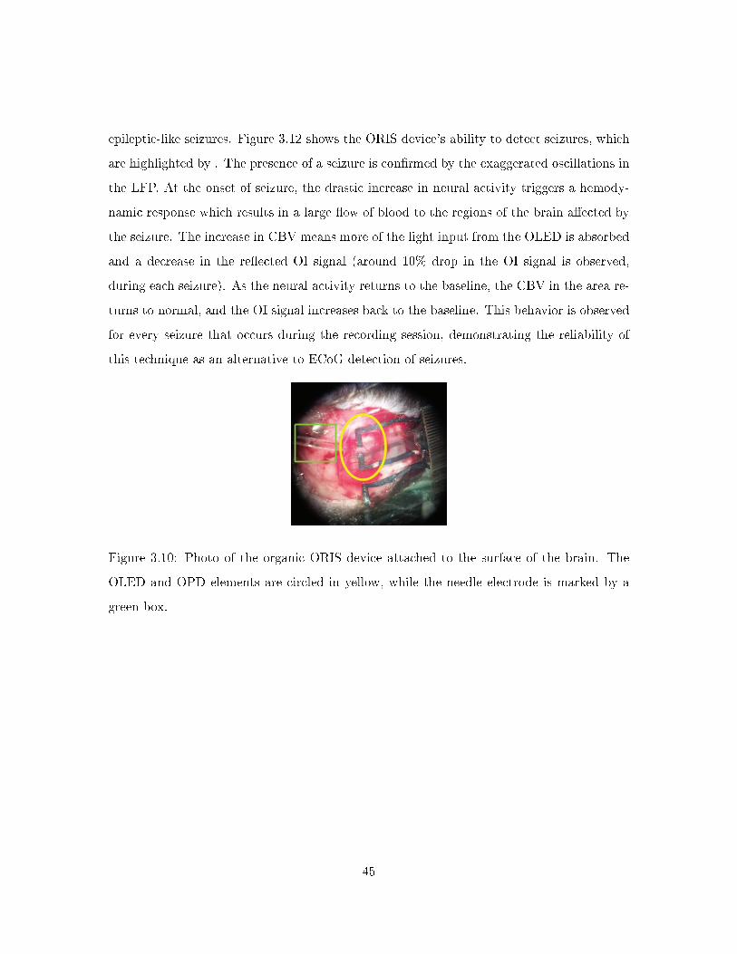
epileptic-like seizures. Figure 3.12 shows the ORIS device's ability to detect seizures, which
are highlighted by . The presence of a seizure is con�rmed by the exaggerated oscillations in
the LFP. At the onset of seizure, the drastic increase in neural activity triggers a hemody-
namic response which results in a large �ow of blood to the regions of the brain a�ected by
the seizure. The increase in CBV means more of the light input from the OLED is absorbed
and a decrease in the re�ected OI signal (around 10% drop in the OI signal is observed,
during each seizure). As the neural activity returns to the baseline, the CBV in the area re-
turns to normal, and the OI signal increases back to the baseline. This behavior is observed
for every seizure that occurs during the recording session, demonstrating the reliability of
this technique as an alternative to ECoG detection of seizures.
Figure 3.10: Photo of the organic ORIS device attached to the surface of the brain. The
OLED and OPD elements are circled in yellow, while the needle electrode is marked by a
green box.
45
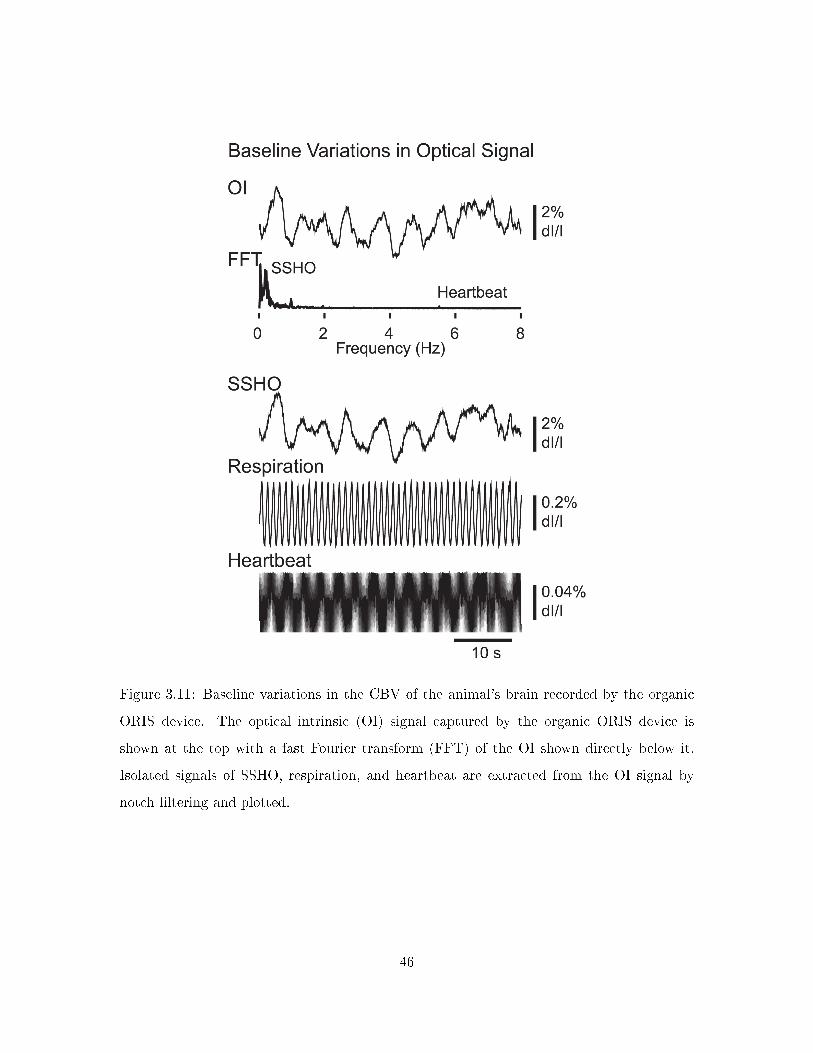
Figure 3.11: Baseline variations in the CBV of the animal's brain recorded by the organic
ORIS device. The optical intrinsic (OI) signal captured by the organic ORIS device is
shown at the top with a fast Fourier transform (FFT) of the OI shown directly below it.
Isolated signals of SSHO, respiration, and heartbeat are extracted from the OI signal by
notch �ltering and plotted.
46
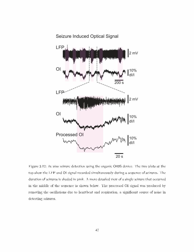
Figure 3.12: In vivo seizure detection using the organic ORIS device. The two plots at the
top show the LFP and OI signal recorded simultaneously during a sequence of seizures. The
duration of seizures is shaded in pink. A more detailed view of a single seizure that occurred
in the middle of the sequence is shown below. The processed OI signal was produced by
removing the oscillations due to heartbeat and respiration, a signi�cant source of noise in
detecting seizures.
47
3.6 Chapter Summary
In this chapter, an organic-based implantable ORIS sensor for in vivo detection of seizures
was discussed. The complete device included OLEDs and OPDs fabricated on a biocom-
patible, free standing parylene-c substrate with a total thickness under 5 µm, including
encapsulation. The �exibility, performance, and seizure detection ability of the device was
discussed, demonstrating the potential for application as a clinical alternative to ECoG
measurement of neural activity.
48

Chapter 4
MicroLED Based Sensor
4.1 Bi-directional Emitter/Detector MicroLEDs
The commercial microLEDs used in this work are CREE DA1000 and CREE DA850 LEDs.
The unique feature of these microLEDs are preformed AuSn solder bumps for eutectic die
attach. This allows the microLEDs to be soldered to a substrate or circuit by aligning and
heating the chips without the need to place solder on the bond pads. The DA 1000 LEDs
have dimensions of 1 mm x 1 mm x 335µm . The DA 850 LEDs have dimensions of 850 µm
x 850 µm x 335 µm.
Figure 4.1: Photograph of the microLEDs soldered onto a glass substrate with a Cr/Au
circuit. DA1000 LED (left) is 1 mm in length. DA 850 (right) is 850 µm in length.
49
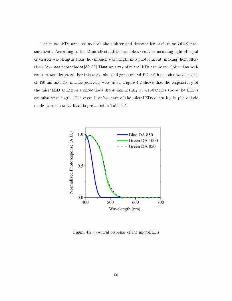
The microLEDs are used as both the emitter and detector for performing ORIS mea-
surements. According to the Mims e�ect, LEDs are able to convert incoming light of equal
or shorter wavelengths than the emission wavelength into photocurrent, making them e�ec-
tively low-pass photodiodes.[32, 33] Thus, an array of microLEDs can be multiplexed as both
emitters and detectors. For this work, blue and green microLEDs with emission wavelengths
of 450 nm and 530 nm, respectively, were used. Figure 4.2 shows that the responsivity of
the microLED acting as a photodiode drops signi�cantly at wavelengths above the LED's
emission wavelength. The overall performance of the microLEDs operating in photodiode
mode (zero electrical bias) is presented in Table 4.1.
400 500 600 7000.0
0.5
1.0
Nor
mal
ized
Pho
tore
spon
se (A
.U.)
Wavelength (nm)
Blue DA 850 Green DA 1000 Green DA 850
Figure 4.2: Spectral response of the microLEDs
50
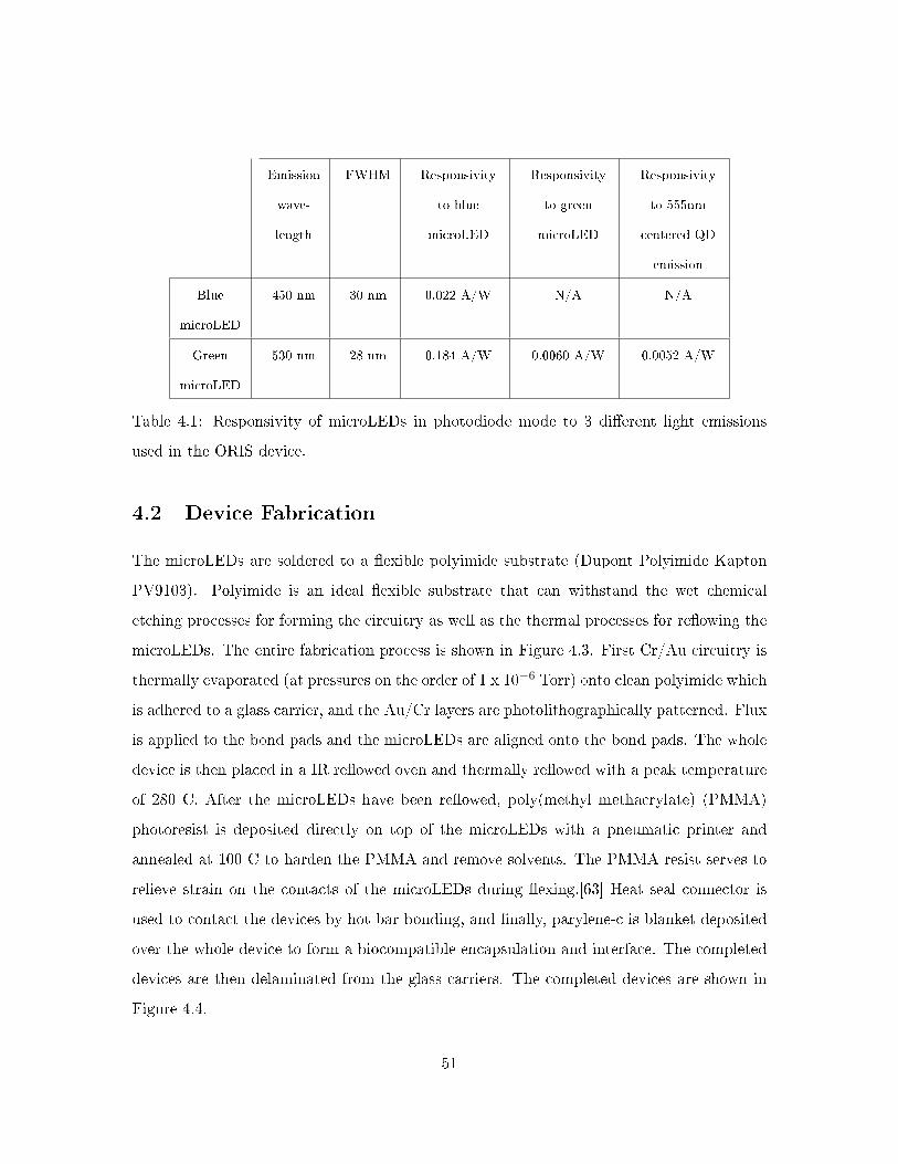
Emission
wave-
length
FWHM Responsivity
to blue
microLED
Responsivity
to green
microLED
Responsivity
to 555nm
centered QD
emission
Blue
microLED
450 nm 30 nm 0.022 A/W N/A N/A
Green
microLED
530 nm 28 nm 0.184 A/W 0.0060 A/W 0.0052 A/W
Table 4.1: Responsivity of microLEDs in photodiode mode to 3 di�erent light emissions
used in the ORIS device.
4.2 Device Fabrication
The microLEDs are soldered to a �exible polyimide substrate (Dupont Polyimide Kapton
PV9103). Polyimide is an ideal �exible substrate that can withstand the wet chemical
etching processes for forming the circuitry as well as the thermal processes for re�owing the
microLEDs. The entire fabrication process is shown in Figure 4.3. First Cr/Au circuitry is
thermally evaporated (at pressures on the order of 1 x 10⁻⁶ Torr) onto clean polyimide which
is adhered to a glass carrier, and the Au/Cr layers are photolithographically patterned. Flux
is applied to the bond pads and the microLEDs are aligned onto the bond pads. The whole
device is then placed in a IR re�owed oven and thermally re�owed with a peak temperature
of 280 C. After the microLEDs have been re�owed, poly(methyl methacrylate) (PMMA)
photoresist is deposited directly on top of the microLEDs with a pneumatic printer and
annealed at 100 C to harden the PMMA and remove solvents. The PMMA resist serves to
relieve strain on the contacts of the microLEDs during �exing.[63] Heat seal connector is
used to contact the devices by hot bar bonding, and �nally, parylene-c is blanket deposited
over the whole device to form a biocompatible encapsulation and interface. The completed
devices are then delaminated from the glass carriers. The completed devices are shown in
Figure 4.4.
51
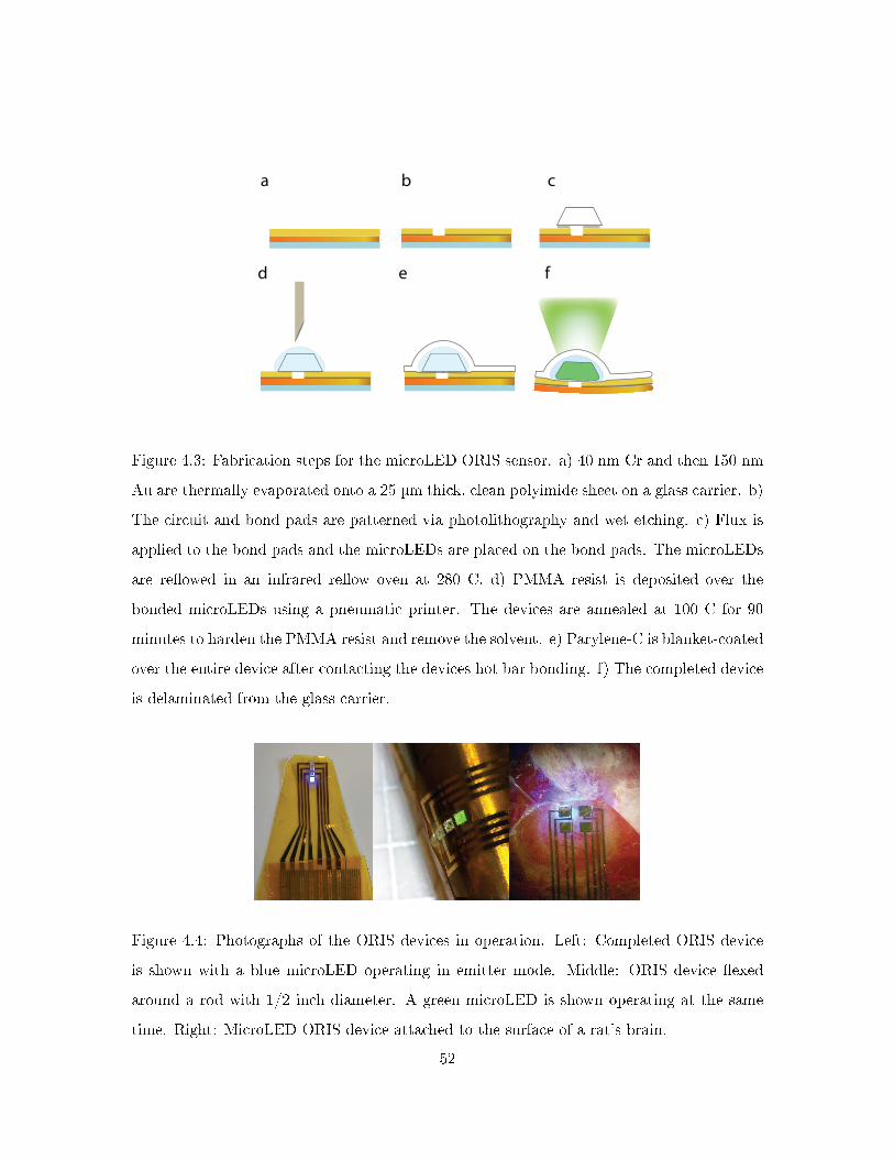
a b c
d e f
Figure 4.3: Fabrication steps for the microLED ORIS sensor. a) 40 nm Cr and then 150 nm
Au are thermally evaporated onto a 25 µm thick, clean polyimide sheet on a glass carrier. b)
The circuit and bond pads are patterned via photolithography and wet etching. c) Flux is
applied to the bond pads and the microLEDs are placed on the bond pads. The microLEDs
are re�owed in an infrared re�ow oven at 280 C. d) PMMA resist is deposited over the
bonded microLEDs using a pneumatic printer. The devices are annealed at 100 C for 90
minutes to harden the PMMA resist and remove the solvent. e) Parylene-C is blanket-coated
over the entire device after contacting the devices hot bar bonding. f) The completed device
is delaminated from the glass carrier.
Figure 4.4: Photographs of the ORIS devices in operation. Left: Completed ORIS device
is shown with a blue microLED operating in emitter mode. Middle: ORIS device �exed
around a rod with 1/2 inch diameter. A green microLED is shown operating at the same
time. Right: MicroLED ORIS device attached to the surface of a rat's brain.
52
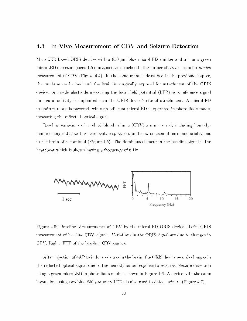
4.3 In-Vivo Measurement of CBV and Seizure Detection
MicroLED-based ORIS devices with a 850 µm blue microLED emitter and a 1 mm green
microLED detector spaced 1.5 mm apart are attached to the surface of a rat's brain for in vivo
measurement of CBV (Figure 4.4). In the same manner described in the previous chapter,
the rat is anaesthetized and the brain is surgically exposed for attachment of the ORIS
device. A needle electrode measuring the local �eld potential (LFP) as a reference signal
for neural activity is implanted near the ORIS device's site of attachment. A microLED
in emitter mode is powered, while an adjacent microLED is operated in photodiode mode,
measuring the re�ected optical signal.
Baseline variations of cerebral blood volume (CBV) are measured, including hemody-
namic changes due to the heartbeat, respiration, and slow sinusoidal harmonic oscillations
in the brain of the animal (Figure 4.5). The dominant element in the baseline signal is the
heartbeat which is shown having a frequency of 6 Hz.
1 sec
Figure 4.5: Baseline Measurements of CBV by the microLED ORIS device. Left: ORIS
measurement of baseline CBV signals. Variations in the ORIS signal are due to changes in
CBV. Right: FFT of the baseline CBV signals.
After injection of 4AP to induce seizures in the brain, the ORIS device records changes in
the re�ected optical signal due to the hemodynamic response to seizures. Seizure detection
using a green microLED in photodiode mode is shown in Figure 4.6. A device with the same
layout but using two blue 850 µm microLEDs is also used to detect seizure (Figure 4.7).
53
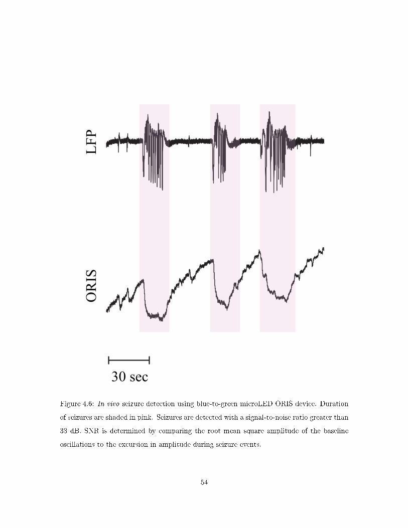
30 sec
LF
PO
RIS
Figure 4.6: In vivo seizure detection using blue-to-green microLED ORIS device. Duration
of seizures are shaded in pink. Seizures are detected with a signal-to-noise ratio greater than
33 dB. SNR is determined by comparing the root mean square amplitude of the baseline
oscillations to the excursion in amplitude during seizure events.
54
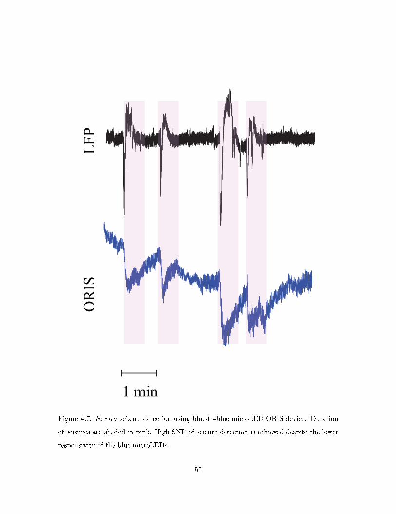
1 min
LF
PO
RIS
Figure 4.7: In vivo seizure detection using blue-to-blue microLED ORIS device. Duration
of seizures are shaded in pink. High SNR of seizure detection is achieved despite the lower
responsivity of the blue microLEDs.
55

At the onset of each seizure, blood rushes to the site of the seizure in response to the
increased neural activity resulting in a dip in the ORIS signal collected by the microLED in
photodiode mode. As the neural activity returns to the baseline, the CBV levels decrease
and the ORIS signal relaxes towards the baseline level. The blue-to-green ORIS device was
able to detect seizures with a signal-to-noise ratio (SNR) greater than 33 dB. The blue-
to-blue device has a similarly high SNR greater than 18 dB, despite the lower responsivity
of the blue microLEDs in photodiode mode since the heartbeat signal presents the largest
source of noise for seizure detection and the amplitude of heartbeat oscillations decreases
with the lower responsivity of the blue microLED detectors.
Another device with 4 microLED elements con�gured in a linear array is attached to
a rat's brain for detecting localized changes in CBV during seizures. The layout for this
device is shown in Figure 4.8. 2 green microLEDs, PD1 and PD2, operate in photodiode
mode measuring the re�ected ORIS signal, while 2 blue microLEDs operate in emitter
mode. PD1, which is closer to the focus of the seizure, observes an increase in CBV and
relaxation back to the baseline with each seizure that occurs. PD2 detects di�erent changes
in CBV at the site of attachment. The recorded CBV changes with varying amplitude
and duration due to dynamic metabolic demands of the brain during seizures of di�erent
severity. This localized hemodynamic response, shown in Figure 4.9, is consistent with earlier
observed measurements of CBV.[29] This demonstration of localization of hemodynamic
changes during seizure events shows the potential of the microLED ORIS device to be
used for large area, high resolution imaging of neural activity. By using a full 2D array
of microLEDs in this device architecture, spatial resolutions on the order of 1 mm x 1
mm are possible. Further, by switching to smaller microLED elements, spatial resolutions
approaching those achieved with CCD cameras ( < 200 µm) may be possible. This kind
of performance at high resolutions would be comparable to advanced ECoG arrays with
sub-millimeter inter-electrode spacing.[20, 21]
56
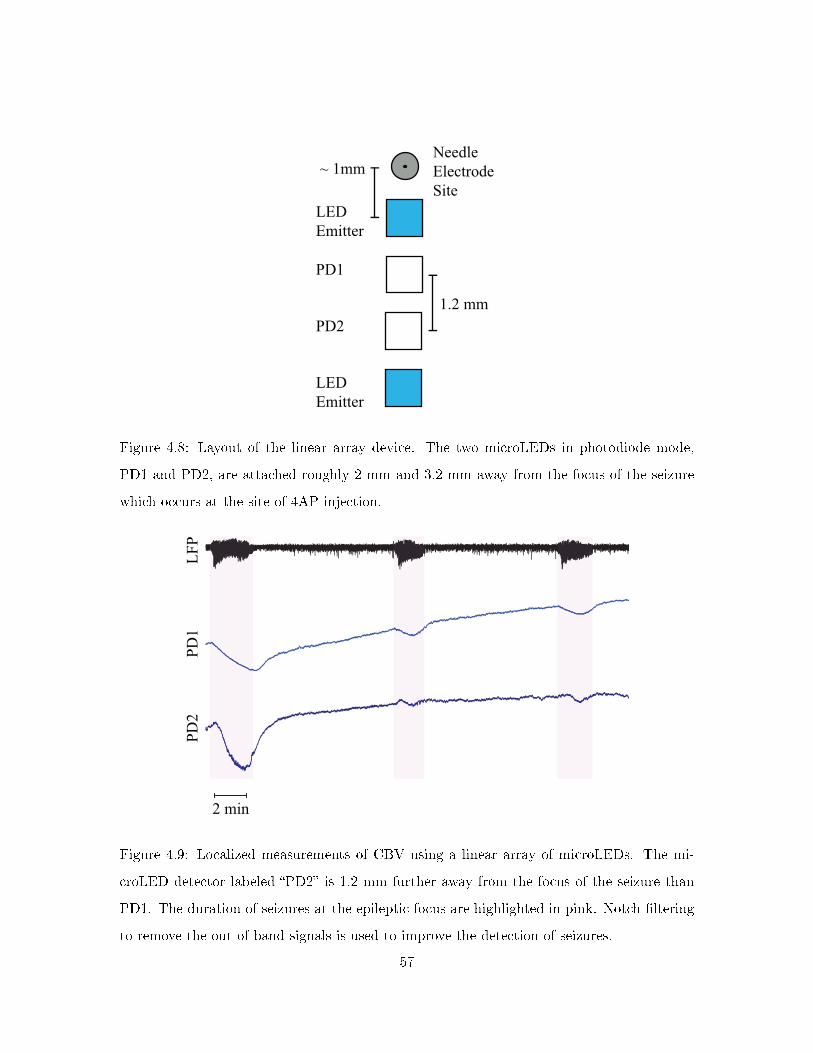
LED
Emitter
PD1
PD2
LED
Emitter
Needle
Electrode
Site
~ 1mm
1.2 mm
Figure 4.8: Layout of the linear array device. The two microLEDs in photodiode mode,
PD1 and PD2, are attached roughly 2 mm and 3.2 mm away from the focus of the seizure
which occurs at the site of 4AP injection.
2 min
LF
PP
D1
PD
2
Figure 4.9: Localized measurements of CBV using a linear array of microLEDs. The mi-
croLED detector labeled �PD2� is 1.2 mm further away from the focus of the seizure than
PD1. The duration of seizures at the epileptic focus are highlighted in pink. Notch �ltering
to remove the out of band signals is used to improve the detection of seizures.
57
4.4 MicroLED ORIS Sensor with Quantum Dot Optical Down-
Conversion Coating
In order to select emission wavelengths outside of the discrete wavelengths available for com-
mercial microLEDs, quantum dot (QD) composite coatings are applied to microLEDs via
pneumatic printing. CdS/CdSe/CdS core shell quantum dots are suspended in toluene at
a concentration of 20 mg/mL. The QD:PMMA composite is prepared by mixing an equal
weight of the QD (in toluene) solution with 950 A6 PMMA photoresist (MicroChem). The
mixture is heated at 70 C for 45 minutes while being stirred with a magnetic stir bar to
increase the viscosity. The fabrication of the devices with the QD coatings is identical to
the one described above (Figure 4.3), with the QD:PMMA composite replacing PMMA pho-
toresist. By utilizing the pneumatic printing technique described in Yang et al.,[90] the QD
coatings can be applied to individual microLEDs without a�ecting adjacent elements, allow-
ing for the use of multiple emission wavelengths using only blue microLEDs. Photographs
of the printing set up and microLEDs with applied QD coatings is shown in Figure 4.10.
Figure 4.11 shows the emission spectra for the microLEDs directly after the QD coatings
have been applied. Some of the blue backlight is emitted out due to both light leaking
through the QD coating and back-re�ections from the subsrate, but the QD coatings are able
to perform well as color conversion layers with the addition of a color �lter for removing the
blue backlight. . For the amber QD coating, 86.2% of the emitted light is down-converted.
For the red QD coating 95.5% of the emitted light is down-converted. For the green QD
coating 89.5% of the emitted light is down-converted. Conversion percentage is calculated
by comparing the integral of light intensity in the 500 nm to 750 nm range to the integral
of light intensity over the entire spectral range.
58
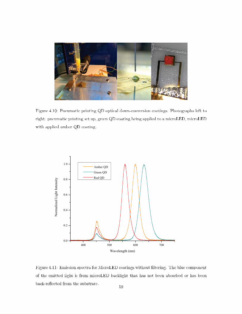
Figure 4.10: Pneumatic printing QD optical down-conversion coatings. Photographs left to
right: pneumatic printing set up, green QD coating being applied to a microLED, microLED
with applied amber QD coating.
400 500 600 7000.0
0.2
0.4
0.6
0.8
1.0
Nor
mal
ized
Lig
ht In
tens
ity
Wavelength (nm)
Amber QD
Green QD
Red QD
Figure 4.11: Emission spectra for MicroLED coatings without �ltering. The blue component
of the emitted light is from microLED backlight that has not been absorbed or has been
back-re�ected from the substrate.59
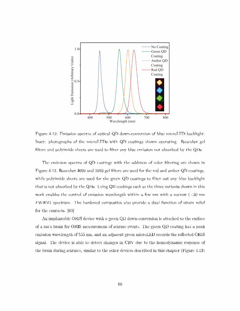
Figure 4.12: Emission spectra of optical QD down-conversion of blue microLED backlight.
Inset: photographs of the microLEDs with QD coatings shown operating. Roscolux gel
�lters and polyimide sheets are used to �lter any blue emission not absorbed by the QDs.
The emission spectra of QD coatings with the addition of color �ltering are shown in
Figure 4.12. Roscolux 4690 and 2003 gel �lters are used for the red and amber QD coatings,
while polyimide sheets are used for the green QD coatings to �lter out any blue backlight
that is not absorbed by the QDs. Using QD coatings such as the three variants shown in this
work enables the control of emission wavelength within a few nm with a narrow (<50 nm
FWHM) spectrum. The hardened composites also provide a dual function of strain relief
for the contacts. [63]
An implantable ORIS device with a green QD down-conversion is attached to the surface
of a rat's brain for ORIS measurement of seizure events. The green QD coating has a peak
emission wavelength of 555 nm, and an adjacent green microLED records the re�ected ORIS
signal. The device is able to detect changes in CBV due to the hemodynamic response of
the brain during seizures, similar to the other devices described in this chapter (Figure 4.13)
60
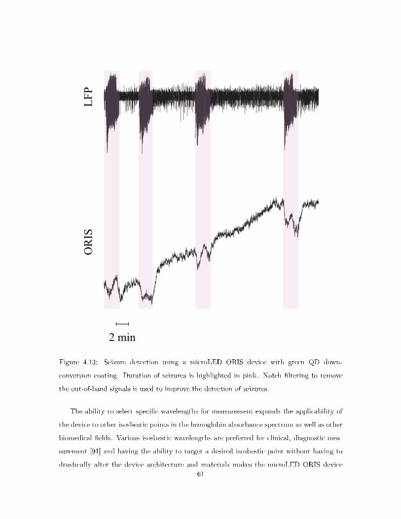
2 min
LF
PO
RIS
Figure 4.13: Seizure detection using a microLED ORIS device with green QD down-
conversion coating. Duration of seizures is highlighted in pink. Notch �ltering to remove
the out-of-band signals is used to improve the detection of seizures.
The ability to select speci�c wavelengths for measurement expands the applicability of
the device to other isosbestic points in the hemoglobin absorbance spectrum as well as other
biomedical �elds. Various isosbestic wavelengths are preferred for clinical, diagnostic mea-
surement [91] and having the ability to target a desired isosbestic point without having to
drastically alter the device architecture and materials makes the microLED ORIS device61
a versatile choice for clinical and biomedical research applications. Additionally, applica-
tions such as pulse-oximetry which requires simultaneous measurement of non-isosbestic
points and the measurement of fetal hemglobin, which has a di�erent absorbance spec-
trum than adult hemoglobin, may bene�t from this device architecture.[92] An implantable
ORIS monitoring device can even be con�gured to provide optogenetic-triggered inhibition
of seizures.[93]
4.5 Chapter Summary
An ORIS device comprised of bi-directional microLED emitter/detector pairs integrated
on a �exible polyimide substrate are presented. Localization of hemodynamic response
to seizures is reported as well as the use of QD optical down-conversion coatings. The
device presented in this chapter has potential for being a next-generation alternative to
clinical ECoG measurement for the diagnosis and treatment of epilepsy, as well as other
applications.
62
Chapter 5
Conclusion
Wearable and implantable sensors have great promise for enabling the next generation of
healthcare diagnostics and treatment methods. Although there has been great excitement
over the bene�ts of computational analysis in personalized healthcare, improvements in
hardware and sensing applications are necessary for extracting relevant, practical data. This
is especially true for surgeons and researchers studying epilepsy. Improvements over current
clinical methods for neuronal mapping have the potential to drastically improve the success
of surgical treatments that involve resection of brain matter. Implantable sensors performing
ORIS measurements of CBV and other factors in the brain have the potential to provide
an alternative method for high spatiotemporal resolution of neuronal activity in clinical
settings.
The work presented here has advanced the development of an implantable optical sensor
for performing ORIS mapping in the brain. These advances include: the design, fabrication,
and testing of implantable ORIS devices using organic LEDs, organic photodetectors, and
microLEDs on a variety of �exible substrates. The demonstrated organics based devices
like the one described in Chapter 3 may be useful for acute clinical measurements and
applications outside of ORIS measurement which require extreme levels of �exibility and
low device thickness. The demonstration of a �exible microLED-based sensor is a candidate
for long-term, chronic measurments of CBV and neuronal activity, thanks to its high optical
performance and long operational lifetimes. Moreover, the localization of seizure activity
in the brain using an arrayed microLED ORIS sensor is a crucial step in achieving full 2D63

mapping of neuronal activity with an implantable ORIS sensor. Finally, the application of
quantum dots to the �exible microLED sensor has extended the functionality of such devices,
by increasing the e�ective range of available emission wavelengths produced by commercial
microLEDs.
Much work remains in developing an implantable ORIS system capable of high spa-
tiotemporal, 2D mapping of neuronal activity. In addition to continued advancement of the
hardware, combining the sensors developed in this work with advanced computational and
analysis methods may provide even higher �delity sensing and open the devices to new appli-
cations. With continued development, an �optical pacemaker� for the brain may eventually
be achieved. Such a device would couple the continuous monitoring of neuronal activity the
ability to locally administer treatments such as optogenetic-triggered neuronal inhibition,
drug delivery, or electric stimulation. This would mark a true leap in the diagnosis and
treatment of neurological diseases such as epilepsy.
64
Publications and Presentations
1. Christopher Choi, Aida R. Colón-Berríos, Leslie S. Hamachi, Jonathan S. Owen,
Theodore H. Schwartz, Hongtao Ma, and Ioannis Kymissis. "Localizing Seizure Activity
in the Brain Using Implantable Micro-LEDs with Quantum Dot Downconversion."
Advanced Materials Technologies (2018): 1700366.
2. Brigitte Holzer, Johannes Bintinger, Daniel Lumpi, Christopher Choi, Youngwan
Kim, Berthold Stöger, Christian Hametner et al. "Color Fine-Tuning of Optical Materials
Through Rational Design." ChemPhysChem 18, no. 5 (2017): 549-563.
3. Youngwan Kim, Christopher Choi, En-Chen Chen, Andy G. S. Daniel, Amrita
Masurkar, Theodore H. Schwartz, Hongtao Ma, Andreas H. Hielscher and Ioannis
Kymissis. (2016, May). �Ultra-thin, Flexible, and Implantable Optical Sensor.� Poster
presented at Display Week 2016, Innovation Zone. San Francisco, CA.
4. Youngwan Kim, Christopher Choi, En-Chen Chen, Andy G. S. Daniel, Amrita
Masurkar, Theodore H. Schwartz, Hongtao Ma, and Ioannis Kymissis. (2016, April). �An
Ultra Thin Implantable System for Cerebral Blood Volume Monitoring Using Flexible
OLED and OPD.� Presented at the 25th annual Connecticut Microelectronics and
Optoelectronics Consortium. Storrs, CT.
5. Youngwan Kim, Christopher Choi, En-Chen Chen, Andy GS Daniel, Amrita
Masurkar, Theodore H. Schwartz, Hongtao Ma, and Ioannis Kymissis. "An ultra thin
implantable system for cerebral blood volume monitoring using �exible OLED and OPD."
In Electron Devices Meeting (IEDM), 2015 IEEE International, pp. 29-6. IEEE, 2015.
65

Bibliography
[1] Annalisa Bon�glio, Ileana Manunza, Alessandra Caboni, Werther Cambarau, and Mas-
simo Barbaro. Organic �eld-e�ect based sensors for body parameters monitoring. Proc.
SPIE Photon, pages 665904�1, 2007.
[2] Claire M Lochner, Yasser Khan, Adrien Pierre, and Ana C Arias. All-organic optoelec-
tronic sensor for pulse oximetry. Nature communications, 5:5745, 2014.
[3] Hyunsu Cho, Changhun Yun, Jae-Woo Park, and Seunghyup Yoo. Highly �exible
organic light-emitting diodes based on zns/ag/wo 3 multilayer transparent electrodes.
Organic Electronics, 10(6):1163�1169, 2009.
[4] Xiaochen Ren, Ke Pei, Boyu Peng, Zhichao Zhang, Zongrong Wang, Xinyu Wang, and
Paddy KL Chan. A low-operating-power and �exible active-matrix organic-transistor
temperature-sensor array. Advanced Materials, 28(24):4832�4838, 2016.
[5] Tomoyuki Yokota, Peter Zalar, Martin Kaltenbrunner, Hiroaki Jinno, Naoji Matsuhisa,
Hiroki Kitanosako, Yutaro Tachibana, Wakako Yukita, Mari Koizumi, and Takao
Someya. Ultra�exible organic photonic skin. Science advances, 2(4):e1501856, 2016.
[6] Ingrid Graz, Markus Krause, Simona Bauer-Gogonea, Siegfried Bauer, Stephanie P
Lacour, Bernd Ploss, Martin Zirkl, Barbara Stadlober, and Sigurd Wagner. Flexible
active-matrix cells with selectively poled bifunctional polymer-ceramic nanocomposite
for pressure and temperature sensing skin. Journal of Applied Physics, 106(3):034503,
2009.
[7] Kyriaki Manoli, Gerardo Palazzo, Eleonora Macchia, Amber Tiwari, Cinzia Di Franco,66
Gaetano Scamarcio, Pietro Favia, Antonia Mallardi, and Luisa Torsi. Electrolyte gated
tft biosensors based on the donnan's capacitance of anchored biomolecules. In Organic
Sensors and Bioelectronics X, volume 10364, page 103640J. International Society for
Optics and Photonics, 2017.
[8] Ileana Manunza, Emanuele Orgiu, Alessandra Caboni, Massimo Barbaro, and Annalisa
Bon�glio. Producing smart sensing �lms by means of organic �eld e�ect transistors.
In Engineering in Medicine and Biology Society, 2006. EMBS'06. 28th Annual Inter-
national Conference of the IEEE, pages 4344�4346. IEEE, 2006.
[9] Yilin Song, Jonathan Viventi, and Yao Wang. Unsupervised learning of spike patterns
for seizure detection and wavefront estimation of high resolution micro electrocortico-
graphic ({\mu} ecog) data. arXiv preprint arXiv:1706.00780, 2017.
[10] B Samanta and C Nataraj. Automated diagnosis of cardiac state in healthcare systems
using computational intelligence. International Journal of Services Operations and
Informatics, 3(2):162�177, 2008.
[11] Monica Tentori and Jesus Favela. Activity-aware computing for healthcare. IEEE
Pervasive Computing, 7(2), 2008.
[12] Epilepsy fact sheet. http://www.who.int/mediacentre/factsheets/fs999/en/, 02 2017.
World Health Organization Website.
[13] Marvin M Goldenberg. Overview of drugs used for epilepsy and seizures: etiology,
diagnosis, and treatment. Pharmacy and Therapeutics, 35(7):392, 2010.
[14] Edward B Brom�eld, José E Cavazos, and Joseph I Sirven. An introduction to epilepsy.
American Epilepsy Society, 2006.
[15] Daniel H. Lowenstein. Seizures and Epilepsy, chapter 369. The McGraw-Hill Compa-
nies, New York, NY, 2012.
[16] Blausen Sta�. Medical gallery of blausen medical 2014. WikiJournal of Medicine,
1(2):10, 2014.
67
[17] Robert S Fisher, Barbara G Vickrey, Patricia Gibson, Bruce Hermann, Patricia Pen-
ovich, Ann Scherer, and Steven Walker. The impact of epilepsy from the patient's
perspective i. descriptions and subjective perceptions. Epilepsy research, 41(1):39�51,
2000.
[18] H Lüders, I Awad, R Burgess, E Wyllie, and P Van Ness. Subdural electrodes in the
presurgical evaluation for surgery of epilepsy. Epilepsy Research. Supplement, 5:147�
156, 1992.
[19] Taro Kaiju, Keiichi Doi, Masashi Yokota, Kei Watanabe, Masato Inoue, Hiroshi Ando,
Kazutaka Takahashi, Fumiaki Yoshida, Masayuki Hirata, and Takafumi Suzuki. High
spatiotemporal resolution ecog recording of somatosensory evoked potentials with �ex-
ible micro-electrode arrays. Frontiers in neural circuits, 11, 2017.
[20] Dion Khodagholy, Jennifer N Gelinas, Thomas Thesen, Werner Doyle, Orrin Devinsky,
George G Malliaras, and György Buzsáki. Neurogrid: recording action potentials from
the surface of the brain. Nature neuroscience, 18(2):310�315, 2015.
[21] Dion Khodagholy, Jennifer N Gelinas, Zifang Zhao, Malcolm Yeh, Michael Long,
Jeremy D Greenlee, Werner Doyle, Orrin Devinsky, and György Buzsáki. Organic elec-
tronics for high-resolution electrocorticography of the human brain. Science Advances,
2(11):e1601027, 2016.
[22] Subhas Chandra Mukhopadhyay. Wearable sensors for human activity monitoring: A
review. IEEE sensors journal, 15(3):1321�1330, 2015.
[23] Xudong Ji, Ho Yuen Lau, Xiaochen Ren, Boyu Peng, Peng Zhai, Shien-Ping Feng, and
Paddy KL Chan. Bioelectronics: Highly sensitive metabolite biosensor based on or-
ganic electrochemical transistor integrated with micro�uidic channel and poly (n-vinyl-
2-pyrrolidone)-capped platinum nanoparticles (adv. mater. technol. 5/2016). Advanced
Materials Technologies, 1(5), 2016.
[24] Danilo Pani, Alessia Dessì, Jose F Saenz-Cogollo, Gianluca Barabino, Beatrice Fraboni,
and Annalisa Bon�glio. Fully textile, pedot: Pss based electrodes for wearable ecg
68
monitoring systems. IEEE Transactions on Biomedical Engineering, 63(3):540�549,
2016.
[25] TAGA Bonhoe�er. Optical imaging based on intrinsic signals the methodology. Brain
mapping: The methods, pages 55�97, 1996.
[26] Theodore H Schwartz. The application of optical recording of intrinsic signals to simul-
taneously acquire functional, pathological and localizing information and its potential
role in neurosurgery. Stereotactic and functional neurosurgery, 83(1):36�44, 2005.
[27] Minah Suh, Sonya Bahar, Ashesh D Mehta, and Theodore H Schwartz. Temporal de-
pendence in uncoupling of blood volume and oxygenation during interictal epileptiform
events in rat neocortex. Journal of Neuroscience, 25(1):68�77, 2005.
[28] Minah Suh, Sonya Bahar, Ashesh D Mehta, and Theodore H Schwartz. Blood volume
and hemoglobin oxygenation response following electrical stimulation of human cortex.
Neuroimage, 31(1):66�75, 2006.
[29] Minah Suh, Hongtao Ma, Mingrui Zhao, Saadat Sharif, and Theodore H Schwartz.
Neurovascular coupling and oximetry during epileptic events. Molecular neurobiology,
33(3):181�197, 2006.
[30] Scott Prahl et al. Optical absorption of hemoglobin.
http://omlc.ogi.edu/spectra/hemoglobin/, 1999.
[31] Marshall P Cox, Hongtao Ma, Matthias E Bahlke, Jonathan H Beck, Theodore H
Schwartz, and Ioannis Kymissis. Led-based optical device for chronic in vivo cerebral
blood volume measurement. IEEE transactions on electron devices, 57(1):174�177,
2010.
[32] Forrest M Mims. Siliconnections: Coming of age in the electronic era. McGraw-Hill
Companies, 1986.
[33] Forrest M Mims. LED Circuits and Projects. Howard W. Sams and Co., Inc, 1979.
69
[34] E Menard, Ralph G Nuzzo, and John A Rogers. Bendable single crystal silicon thin
�lm transistors formed by printing on plastic substrates. Applied Physics Letters,
86(9):093507, 2005.
[35] John A Rogers, Takao Someya, and Yonggang Huang. Materials and mechanics for
stretchable electronics. Science, 327(5973):1603�1607, 2010.
[36] Ioannis Kymissis. Organic Field E�ect Transistors: Theory, Fabrication and Charac-
terization. Springer Science & Business Media, 2008.
[37] H Mu, W Li, R Jones, A Steckl, and D Klotzkin. A comparative study of electrode
e�ects on the electrical and luminescent characteristics of alq 3/tpd oled: Improvements
due to conductive polymer (pedot) anode. Journal of Luminescence, 126(1):225�229,
2007.
[38] Takatoshi Tsujimura. OLED display fundamentals and applications. John Wiley &
Sons, 2017.
[39] MAa Baldo, Sb Lamansky, PEc Burrows, MEb Thompson, and SRl Forrest. Very high-
e�ciency green organic light-emitting devices based on electrophosphorescence. Applied
Physics Letters, 75(1):4�6, 1999.
[40] Stefan Kappaun, Christian Slugovc, and Emil JW List. Phosphorescent organic light-
emitting devices: Working principle and iridium based emitter materials. International
journal of molecular sciences, 9(8):1527�1547, 2008.
[41] Hoang-Yan Lin, Yu-Hsuan Ho, Juin-Haw Lee, Kuan-Yu Chen, Jheng-Hao Fang, Sheng-
Chih Hsu, Mao-Kuo Wei, Hung-Yi Lin, Jen-Hui Tsai, and Tung-Chuan Wu. Patterned
microlens array for e�ciency improvement of small-pixelated organic light-emitting
devices. Optics express, 16(15):11044�11051, 2008.
[42] Hyun Soo Kim, Seong Il Moon, Dong Eui Hwang, Ki Won Jeong, Chang Kyo Kim,
Dae-Gyu Moon, and Chinsoo Hong. Novel fabrication method of microlens arrays with
high oled outcoupling e�ciency. Optics & Laser Technology, 77:104�110, 2016.
70
[43] Hany Aziz and Zoran D Popovic. Degradation phenomena in small-molecule organic
light-emitting devices. Chemistry of Materials, 16(23):4522�4532, 2004.
[44] PE Burrows, V Bulovic, SR Forrest, L Sl Sapochak, DM McCarty, and ME Thompson.
Reliability and degradation of organic light emitting devices. Applied Physics Letters,
65(23):2922�2924, 1994.
[45] Wei-Chun Lin, Wei-Ben Wang, Yu-Chin Lin, Bang-Ying Yu, Ying-Yu Chen, Mao-Feng
Hsu, Jwo-Huei Jou, and Jing-Jong Shyue. Migration of small molecules during the
degradation of organic light-emitting diodes. Organic Electronics, 10(4):581�586, 2009.
[46] Qian Yang, Yuying Hao, Zhenguo Wang, Yunfei Li, Hua Wang, and Bingshe Xu.
Double-emission-layer green phosphorescent oled based on lif-doped tpbi as electron
transport layer for improving e�ciency and operational lifetime. Synthetic Metals,
162(3):398�401, 2012.
[47] A Ra Cho, Eun Hye Kim, Soo Young Park, and Lee Soon Park. Flexible oled encapsu-
lated with gas barrier �lm and adhesive gasket. Synthetic Metals, 193:77�80, 2014.
[48] Samuel P Subbarao, Matthias E Bahlke, and Ioannis Kymissis. Laboratory thin-�lm
encapsulation of air-sensitive organic semiconductor devices. IEEE Transactions on
Electron Devices, 57(1):153�156, 2010.
[49] Jay S Lewis and Michael S Weaver. Thin-�lm permeation-barrier technology for �exible
organic light-emitting devices. IEEE Journal of selected topics in quantum electronics,
10(1):45�57, 2004.
[50] Jin-Seong Park, Heeyeop Chae, Ho Kyoon Chung, and Sang In Lee. Thin �lm encapsula-
tion for �exible am-oled: a review. Semiconductor science and technology, 26(3):034001,
2011.
[51] Ross D Jansen-van Vuuren, Ardalan Armin, Ajay K Pandey, Paul L Burn, and Paul
Meredith. Organic photodiodes: the future of full color detection and image sensing.
Advanced Materials, 28(24):4766�4802, 2016.
71
[52] Gordon J Hedley, Alexander J Ward, Alexander Alekseev, Calvyn T Howells, Emil-
iano R Martins, Luis A Serrano, Graeme Cooke, Arvydas Ruseckas, and Ifor DW
Samuel. Determining the optimum morphology in high-performance polymer-fullerene
organic photovoltaic cells. Nature communications, 4:2867, 2013.
[53] Kang-Jun Baeg, Maddalena Binda, Dario Natali, Mario Caironi, and Yong-Young
Noh. Organic light detectors: photodiodes and phototransistors. Advanced materi-
als, 25(31):4267�4295, 2013.
[54] Sung Heum Park, Anshuman Roy, Serge Beaupré, Shinuk Cho, Nelson Coates, Ji Sun
Moon, Daniel Moses, Mario Leclerc, Kwanghee Lee, and Alan J Heeger. Bulk het-
erojunction solar cells with internal quantum e�ciency approaching 100%. Nature
photonics, 3(5):297�302, 2009.
[55] Gang Yu, Jun Gao, Jan C Hummelen, Fred Wudl, and Alan J Heeger. Polymer pho-
tovoltiac cells: Enhanced e�ciencies via a network of internal donor-acceptor hetero-
junctions. Science, 270(5243):1789, 1995.
[56] Szuheng Ho, Shuyi Liu, Ying Chen, and Franky So. Review of recent progress in
multilayer solution-processed organic light-emitting diodes. Journal of Photonics for
Energy, 5(1):057611�057611, 2015.
[57] Claire M Lochner, Yasser Khan, Adrien Pierre, and Ana C Arias. All-organic optoelec-
tronic sensor for pulse oximetry. Nature communications, 5:5745, 2014.
[58] Jason R Wojciechowski, Lisa C Shriver-Lake, Mariko Y Yamaguchi, Erwin Fu�reder,
Roland Pieler, Martin Schamesberger, Christoph Winder, Hans Ju�rgen Prall, Max
Sonnleitner, and Frances S Ligler. Organic photodiodes for biosensor miniaturization.
Analytical chemistry, 81(9):3455�3461, 2009.
[59] Eeshita Manna, Teng Xiao, Joseph Shinar, and Ruth Shinar. Organic photodetectors
in analytical applications. Electronics, 4(3):688�722, 2015.
[60] I Ozden, M Diagne, AV Nurmikko, J Han, and T Takeuchi. A matrix addressable 1024
72

element blue light emitting ingan qw diode array. physica status solidi (a), 188(1):139�
142, 2001.
[61] François Olivier, Anis Daami, Ludovic Dupré, Franck Henry, Bernard Aventurier, and
François Templier. 25-4: Investigation and improvement of 10µm pixel-pitch gan-based
micro-led arrays with very high brightness. In SID Symposium Digest of Technical
Papers, volume 48, pages 353�356. Wiley Online Library, 2017.
[62] HX Jiang and JY Lin. Nitride micro-leds and beyond-a decade progress review. Optics
express, 21(103):A475�A484, 2013.
[63] Junghwan Byun, Byeongmoon Lee, Eunho Oh, Hyunjong Kim, Sangwoo Kim, Seungh-
wan Lee, and Yongtaek Hong. Fully printable, strain-engineered electronic wrap for
customizable soft electronics. Scienti�c Reports, 7:45328, 2017.
[64] V Poher, N Grossman, GT Kennedy, K Nikolic, HX Zhang, Z Gong, EM Drakakis,
E Gu, MD Dawson, PMW French, et al. Micro-led arrays: a tool for two-dimensional
neuron stimulation. Journal of Physics D: Applied Physics, 41(9):094014, 2008.
[65] Kate L Montgomery, Alexander J Yeh, John S Ho, Vivien Tsao, Shrivats Mohan Iyer,
Logan Grosenick, Emily A Ferenczi, Yuji Tanabe, Karl Deisseroth, Scott L Delp, et al.
Wirelessly powered, fully internal optogenetics for brain, spinal and peripheral circuits
in mice. Nature methods, 12(10):969�974, 2015.
[66] Christian Goÿler, Colin Bierbrauer, Rüdiger Moser, Michael Kunzer, Katarzyna Holc,
Wilfried Pletschen, Klaus Köhler, Joachim Wagner, Michael Schwaerzle, Patrick
Ruther, et al. Gan-based micro-led arrays on �exible substrates for optical cochlear
implants. Journal of Physics D: Applied Physics, 47(20):205401, 2014.
[67] Sowmya Venkataramani, Kristina M Davitt, Jiayi Zhang, Heng Xu, Yoon-Kyu Song,
Barry W Connors, and Arto V Nurmikko. Compact semiconductor light-emitting diodes
for dynamic imaging of neuronal circuitry. IEEE Journal of selected topics in quantum
electronics, 11(4):785�790, 2005.
73
[68] Yuejun Chen, Man Xiong, and Su-Chun Zhang. Illuminating parkinson's therapy with
optogenetics. Nature biotechnology, 33(2):149, 2015.
[69] B Zorman, Mushti V Ramakrishna, and RA Friesner. Quantum con�nement e�ects in
cdse quantum dots. The Journal of Physical Chemistry, 99(19):7649�7653, 1995.
[70] Louis Brus. Electronic wave functions in semiconductor clusters: experiment and theory.
The Journal of Physical Chemistry, 90(12):2555�2560, 1986.
[71] Benjamin S Mashford, Tich-Lam Nguyen, Gerard J Wilson, and Paul Mulvaney. All-
inorganic quantum-dot light-emitting devices formed via low-cost, wet-chemical pro-
cessing. Journal of Materials Chemistry, 20(1):167�172, 2010.
[72] JM Caruge, JE Halpert, V Wood, V Bulovi¢, and MG Bawendi. Colloidal quantum-
dot light-emitting diodes with metal-oxide charge transport layers. Nature photonics,
2(4):247�250, 2008.
[73] Yasuhiro Shirasaki, Geo�rey J Supran, Moungi G Bawendi, and Vladimir Bulovi¢.
Emergence of colloidal quantum-dot light-emitting technologies. Nature Photonics,
7(1):13�23, 2013.
[74] Minghui Yang, Alireza Javadi, and Shaoqin Gong. Sensitive electrochemical im-
munosensor for the detection of cancer biomarker using quantum dot functionalized
graphene sheets as labels. Sensors and Actuators B: Chemical, 155(1):357�360, 2011.
[75] Zhexiang Zou, Dan Du, Jun Wang, Jordan N Smith, Charles Timchalk, Yaoqun Li,
and Yuehe Lin. Quantum dot-based immunochromatographic �uorescent biosensor for
biomonitoring trichloropyridinol, a biomarker of exposure to chlorpyrifos. Analytical
chemistry, 82(12):5125�5133, 2010.
[76] Mei Hu, Juan Yan, Yao He, Haoting Lu, Lixing Weng, Shiping Song, Chunhai Fan, and
Lianhui Wang. Ultrasensitive, multiplexed detection of cancer biomarkers directly in
serum by using a quantum dot-based micro�uidic protein chip. ACS nano, 4(1):488�494,
2009.
74
[77] Fei Zhao, Jing Gao, Long Fang, Xia Yin, Xiaofang Jiang, Yehua Su, Yongyin Kang, and
Zhicheng Song. Quantum dots for wide color gamut displays from photoluminescence
to electroluminescence. Nanoscale research letters, 12(1):154, 2017.
[78] Dennis EJGJ Dolmans, Dai Fukumura, and Rakesh K Jain. Photodynamic therapy for
cancer. Nature reviews cancer, 3(5):380, 2003.
[79] Chia-Yen Hsu, Ching-Wen Chen, Hsiu-Ping Yu, Yan-Fu Lin, and Ping-Shan Lai. Bio-
luminescence resonance energy transfer using luciferase-immobilized quantum dots for
self-illuminated photodynamic therapy. Biomaterials, 34(4):1204�1212, 2013.
[80] Min-Kyung So, Chenjie Xu, Andreas M Loening, Sanjiv S Gambhir, and Jianghong Rao.
Self-illuminating quantum dot conjugates for in vivo imaging. Nature biotechnology,
24(3):339, 2006.
[81] Hao Chen, Juan He, Raymond Lanzafame, Istvan Stadler, Hamid El Hamidi, Hui Liu,
Jonathan Celli, Michael R Hamblin, Yingying Huang, Emily Oakley, et al. Quantum
dot light emitting devices for photomedical applications. Journal of the Society for
Information Display, 25(3):177�184, 2017.
[82] Hyunsu Cho, Changhun Yun, Jae-Woo Park, and Seunghyup Yoo. Highly �exible
organic light-emitting diodes based on zns/ag/wo 3 multilayer transparent electrodes.
Organic Electronics, 10(6):1163�1169, 2009.
[83] James A Schwarz, Cristian I Contescu, and Karol Putyera. Dekker encyclopedia of
nanoscience and nanotechnology, volume 3. CRC press, 2004.
[84] Je�rey B Fortin and Toh-Ming Lu. Chemical vapor deposition polymerization: the
growth and properties of parylene thin �lms. Springer Science & Business Media, 2003.
[85] Bo Lu. Parylene as a new membrane material for biomems applications. California
Institute of Technology, 2012.
[86] Youngwan Kim, Christopher Choi, En-Chen Chen, Andy GS Daniel, Amrita Masurkar,
Theodore H Schwartz, Hongtao Ma, and Ioannis Kymissis. An ultra thin implantable
75
system for cerebral blood volume monitoring using �exible oled and opd. In Electron
Devices Meeting (IEDM), 2015 IEEE International, pages 29�6. IEEE, 2015.
[87] Jiangeng Xue, Soichi Uchida, Barry P Rand, and Stephen R Forrest. Asymmetric
tandem organic photovoltaic cells with hybrid planar-mixed molecular heterojunctions.
Applied Physics Letters, 85(23):5757�5759, 2004.
[88] Kristin L Mutolo, Elizabeth I Mayo, Barry P Rand, Stephen R Forrest, and Mark E
Thompson. Enhanced open-circuit voltage in subphthalocyanine/c60 organic photo-
voltaic cells. Journal of the American Chemical Society, 128(25):8108�8109, 2006.
[89] Samuel P Subbarao, Matthias E Bahlke, and Ioannis Kymissis. Laboratory thin-�lm
encapsulation of air-sensitive organic semiconductor devices. IEEE Transactions on
Electron Devices, 57(1):153�156, 2010.
[90] Shyuan Yang, Steve Park, Johannes Bintinger, Yvan Bonnassieux, and Ioannis Kymis-
sis. P-99: Pneumatic nozzle printing as a versatile approach to crystal growth manage-
ment and patterning of printed organic thin �lm transistors. In SID Symposium Digest
of Technical Papers, volume 47, pages 1502�1505. Wiley Online Library, 2016.
[91] Gunter Hoxter. Suggested isosbestic wavelength calibration in clinical analyses. Clinical
chemistry, 25(1):143�146, 1979.
[92] WG Zijlstra, A Buursma, and WP Meeuwsen-Van der Roest. Absorption spectra
of human fetal and adult oxyhemoglobin, de-oxyhemoglobin, carboxyhemoglobin, and
methemoglobin. Clinical chemistry, 37(9):1633�1638, 1991.
[93] Mingrui Zhao, Rose Alleva, Hongtao Ma, Andy GS Daniel, and Theodore H Schwartz.
Optogenetic tools for modulating and probing the epileptic network. Epilepsy research,
116:15�26, 2015.
[94] Antti Hassinen, Iwan Moreels, Kim De Nolf, Philippe F Smet, Jose� C Martins, and
Zeger Hens. Short-chain alcohols strip x-type ligands and quench the luminescence of
pbse and cdse quantum dots, acetonitrile does not. Journal of the American Chemical
Society, 134(51):20705�20712, 2012.76
[95] Byeong Guk Jeong, Young-Shin Park, Jun Hyuk Chang, Ikjun Cho, Jai Kyeong Kim,
Heesuk Kim, Kookheon Char, Jinhan Cho, Victor I Klimov, Philip Park, et al. Col-
loidal spherical quantum wells with near-unity photoluminescence quantum yield and
suppressed blinking. ACS nano, 10(10):9297�9305, 2016.
[96] Margaret A Hines and Philippe Guyot-Sionnest. Synthesis and characterization of
strongly luminescing zns-capped cdse nanocrystals. The Journal of Physical Chemistry,
100(2):468�471, 1996.
[97] Leslie S Hamachi, Ilan Jen-La Plante, Aidan C Coryell, Jonathan De Roo, and
Jonathan S Owen. Kinetic control over cds nanocrystal nucleation using a library of
thiocarbonates, thiocarbamates, and thioureas. Chemistry of Materials, 29(20):8711�
8719, 2017.
[98] Yuehui Zhou and Michael K Denk. Synthesis and reactivity of subvalent compounds.
part 13: Reaction of triethyl orthoformate with amines and selenium�a convenient
one-step three-component synthesis for selenoureas. Tetrahedron letters, 44(6):1295�
1299, 2003.
77

Appendix
78
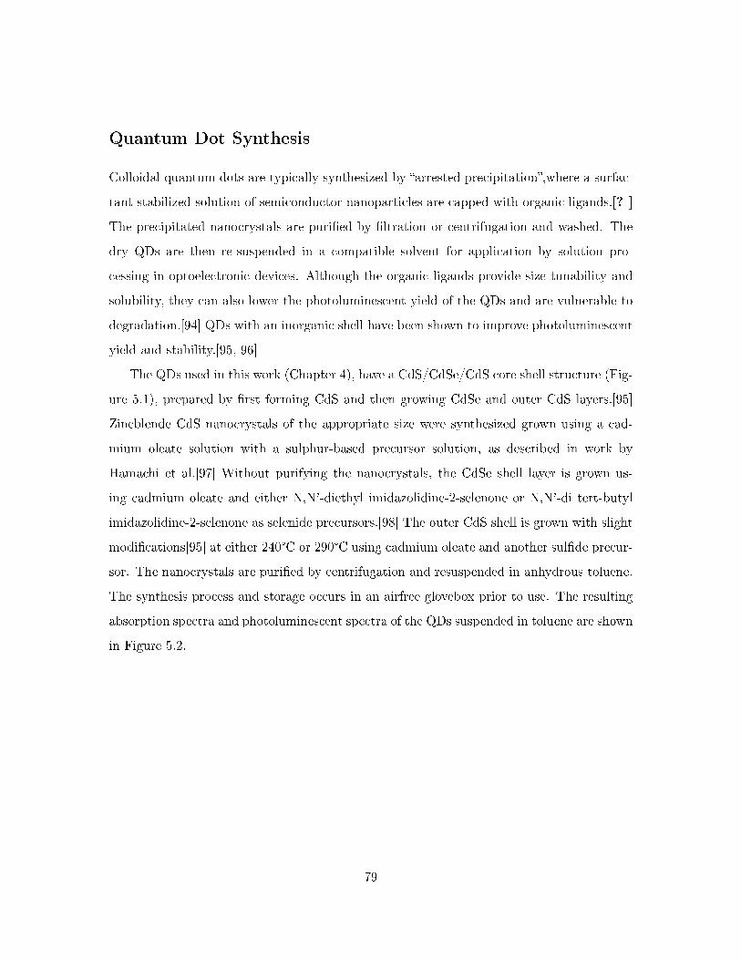
Quantum Dot Synthesis
Colloidal quantum dots are typically synthesized by �arrested precipitation�,where a surfac-
tant stabilized solution of semiconductor nanoparticles are capped with organic ligands.[? ]
The precipitated nanocrystals are puri�ed by �ltration or centrifugation and washed. The
dry QDs are then re-suspended in a compatible solvent for application by solution pro-
cessing in optoelectronic devices. Although the organic ligands provide size tunability and
solubility, they can also lower the photoluminescent yield of the QDs and are vulnerable to
degradation.[94] QDs with an inorganic shell have been shown to improve photoluminescent
yield and stability.[95, 96]
The QDs used in this work (Chapter 4), have a CdS/CdSe/CdS core shell structure (Fig-
ure 5.1), prepared by �rst forming CdS and then growing CdSe and outer CdS layers.[95]
Zincblende CdS nanocrystals of the appropriate size were synthesized grown using a cad-
mium oleate solution with a sulphur-based precursor solution, as described in work by
Hamachi et al.[97] Without purifying the nanocrystals, the CdSe shell layer is grown us-
ing cadmium oleate and either N,N'-diethyl imidazolidine-2-selenone or N,N'-di tert-butyl
imidazolidine-2-selenone as selenide precursors.[98] The outer CdS shell is grown with slight
modi�cations[95] at either 240°C or 290°C using cadmium oleate and another sul�de precur-
sor. The nanocrystals are puri�ed by centrifugation and resuspended in anhydrous toluene.
The synthesis process and storage occurs in an airfree glovebox prior to use. The resulting
absorption spectra and photoluminescent spectra of the QDs suspended in toluene are shown
in Figure 5.2.
79
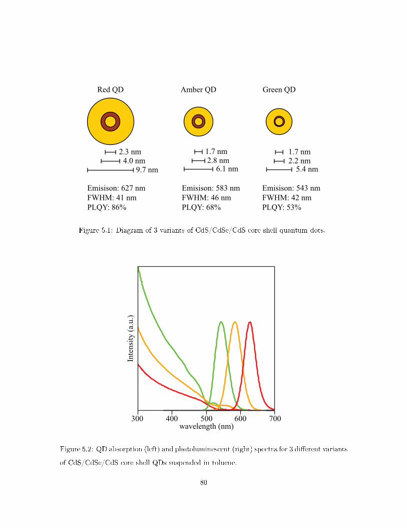
2.3 nm
4.0 nm
9.7 nm
1.7 nm
2.8 nm6.1 nm
1.7 nm
2.2 nm5.4 nm
Red QD Amber QD Green QD
Emisison: 627 nm
FWHM: 41 nm
PLQY: 86%
Emisison: 583 nm
FWHM: 46 nm
PLQY: 68%
Emisison: 543 nm
FWHM: 42 nm
PLQY: 53%
Figure 5.1: Diagram of 3 variants of CdS/CdSe/CdS core shell quantum dots.
Inte
nsi
ty (
a.u.)
700600500400300wavelength (nm)
Figure 5.2: QD absorption (left) and photoluminescent (right) spectra for 3 di�erent variants
of CdS/CdSe/CdS core shell QDs suspended in toluene.
80