Optimum design of IC power/ground nets subject to reliability constraints
10
IEEE TRANSACTIONS ON COMPUTER-AIDED DESIGN. VOL. 7. NO. I, JULY 1988 787 Optimum Design of IC Power/Ground Nets Subject to Reliability Constraints Abstract-This paper formulates and solves the problem of sizing powerlground (p/g) nets in integrated circuits composed of modules, where the nets are routed as trees in the channels between the modules. Constraints are developed in order to maintain proper logic levels and switching speed, to prevent electromigration, and to satisfy certain de- sign rule requirements. Our objective is to minimize the area of the p/g nets subject to these constraints. An optimization technique tai- lored to this problem is developed. The technique solves the problem more efficiently than the steepest descent method and Newton’s method. Several case studies are also presented. I. INTRODUCTION USTOM and semi-custom chips often consist of the C interconnection of logic modules which exist in a cell library. Such modules already have internal power and ground networks which are accessible from outside the modules through some predetermined points (called pins) at the boundary of the modules. The modules are first placed [12] on a carrier (chip) and then the routing of power and ground ( p/g ), clock, and signal nets is carried out in the intermodular spaces, called channels. Routing of p/g nets is often given the first priority, be- cause the p/g wires are usually laid out entirely on a metal layer(s) due to its low resistivity. Signal and clock (com- monly known as signal) nets may share the metal layer(s) with p/g, but they change layers whenever a power or ground wire is encountered along their path. Routing of p/g consists of two main tasks: a) construc- tion of interconnect topologies, and b) determination of width of various segments of the topologies. This paper deals with the second task. (For the first task see [ll], [ 131 , [ 151). The interconnect topologies connect the power (ground) pins of each module to the power (ground) pads of the chip. The structures of these topologies are usually rooted trees, where the root of a power (ground) tree is a power (ground) pad and the leaf nodes of the tree are power (ground) pins on the modules. The tree structures facilitate single-layer routing of power and ground nets without the use of vias. However, to enhance reliability Manuscript received September 8, 1987; revised February 26, 1988. This work was supported in part by the National Science Foundation through its Computer Engineering Program under Grant ECS-83 10774, and in part by its Engineering Initiation Award under Grant MIP-8710751. The review of this paper was arranged by Associate Editor M. R. Lightner. S. Chowdhury is with the Department of Electrical and Computer En- gineering, University of Iowa, Iowa City, IA 52242. M. A. Breuer is with the Department of Electrical Engineering-Systems, University of Southern California, Los Angeles, CA 90089-0781. IEEE Log Number 8821 150. and signal stability, graph structures are preferred, espe- cially for multi-pad and multi-layer p/g distribution sys- tems, In large integrated circuits, such as in VLSI and wafer scale technologies, power and ground distribution is an important problem. Current flow in p/g routes leads to problems of voltage drop and metal migration. Unre- stricted voltage drops may result in incorrect logic oper- ation and degradation is switching speed [5], [14]. Nor- mally power and ground (p/g) nets are routed on the metal layer(s) of a carrier. The life expectancy of such routes is a function of metal migration [2], [6], which is due predominantly to high current densities. Thus, the voltage drops and current densities in p/g routes must be restricted within safe limits. A tree topology constructed for a p/g net has to satisfy these and several other con- straints. Given estimates of currents in the branches of the tree, the attribute of this tree which determines whether the imposed constraints are satisfied or not is the unknown widths of the branches of the tree. The area requirement for p/g nets depends on the limits for allowable voltage drop and current density. The area increases as these limits become more restrictive. Relia- bility considerations require these limits to be kept as small as possible. Hence the p/g routing area for a highly reliable design can be large, especially if the worst-case current requirements for logic modules are considered. Thus, minimizing p/g routing area may be important. In the routing of signal nets, it is normally the practice to attempt to minimize interconnect length. Since the width of signal routes is usually constant, the net effect of minimizing total length is the same as minimizing total area. For power and ground routing this is not the case. The width of each segment of the power and ground routes should be determined so as to minimize the area due to the routes, subject to the constraints imposed. In general, a constant width for all segments will not achieve this goal. This paper addresses the problem of determining the widths of the branches of the p/g trees so as to satisfy all imposed constraints and at the same time minimize the area occupied by the p/g routes. A similar problem re- lated to general graph topologies, rather than just trees, was treated in [5]. The problem of determining the widths is formulated in Section I1 as a nonlinear optimization problem. An algo- rithm for the solution of this problem is presented in Sec- tion 111. Complexity and convergence issues are also dis- 0278-0070/88/0700-0787$01 .OO O 1988 IEEE
Transcript of Optimum design of IC power/ground nets subject to reliability constraints

IEEE TRANSACTIONS ON COMPUTER-AIDED DESIGN. VOL. 7. NO. I , JULY 1988 787
Optimum Design of IC Power/Ground Nets Subject to Reliability Constraints
Abstract-This paper formulates and solves the problem of sizing powerlground (p/g) nets in integrated circuits composed of modules, where the nets are routed as trees in the channels between the modules. Constraints are developed in order to maintain proper logic levels and switching speed, to prevent electromigration, and to satisfy certain de- sign rule requirements. Our objective is to minimize the area of the p/g nets subject to these constraints. An optimization technique tai- lored to this problem is developed. The technique solves the problem more efficiently than the steepest descent method and Newton’s method. Several case studies are also presented.
I. INTRODUCTION USTOM and semi-custom chips often consist of the C interconnection of logic modules which exist in a cell
library. Such modules already have internal power and ground networks which are accessible from outside the modules through some predetermined points (called pins) at the boundary of the modules. The modules are first placed [12] on a carrier (chip) and then the routing of power and ground ( p/g ), clock, and signal nets is carried out in the intermodular spaces, called channels.
Routing of p/g nets is often given the first priority, be- cause the p/g wires are usually laid out entirely on a metal layer(s) due to its low resistivity. Signal and clock (com- monly known as signal) nets may share the metal layer(s) with p/g, but they change layers whenever a power or ground wire is encountered along their path.
Routing of p/g consists of two main tasks: a) construc- tion of interconnect topologies, and b) determination of width of various segments of the topologies. This paper deals with the second task. (For the first task see [ l l ] , [ 131 , [ 151). The interconnect topologies connect the power (ground) pins of each module to the power (ground) pads of the chip. The structures of these topologies are usually rooted trees, where the root of a power (ground) tree is a power (ground) pad and the leaf nodes of the tree are power (ground) pins on the modules. The tree structures facilitate single-layer routing of power and ground nets without the use of vias. However, to enhance reliability
Manuscript received September 8 , 1987; revised February 26, 1988. This work was supported in part by the National Science Foundation through its Computer Engineering Program under Grant ECS-83 10774, and in part by its Engineering Initiation Award under Grant MIP-8710751. The review of this paper was arranged by Associate Editor M. R. Lightner.
S. Chowdhury is with the Department of Electrical and Computer En- gineering, University of Iowa, Iowa City, IA 52242.
M. A. Breuer is with the Department of Electrical Engineering-Systems, University of Southern California, Los Angeles, CA 90089-0781.
IEEE Log Number 8821 150.
and signal stability, graph structures are preferred, espe- cially for multi-pad and multi-layer p/g distribution sys- tems,
In large integrated circuits, such as in VLSI and wafer scale technologies, power and ground distribution is an important problem. Current flow in p/g routes leads to problems of voltage drop and metal migration. Unre- stricted voltage drops may result in incorrect logic oper- ation and degradation is switching speed [ 5 ] , [14]. Nor- mally power and ground (p/g) nets are routed on the metal layer(s) of a carrier. The life expectancy of such routes is a function of metal migration [2], [6], which is due predominantly to high current densities. Thus, the voltage drops and current densities in p/g routes must be restricted within safe limits. A tree topology constructed for a p/g net has to satisfy these and several other con- straints. Given estimates of currents in the branches of the tree, the attribute of this tree which determines whether the imposed constraints are satisfied or not is the unknown widths of the branches of the tree.
The area requirement for p/g nets depends on the limits for allowable voltage drop and current density. The area increases as these limits become more restrictive. Relia- bility considerations require these limits to be kept as small as possible. Hence the p/g routing area for a highly reliable design can be large, especially if the worst-case current requirements for logic modules are considered. Thus, minimizing p/g routing area may be important.
In the routing of signal nets, it is normally the practice to attempt to minimize interconnect length. Since the width of signal routes is usually constant, the net effect of minimizing total length is the same as minimizing total area. For power and ground routing this is not the case. The width of each segment of the power and ground routes should be determined so as to minimize the area due to the routes, subject to the constraints imposed. In general, a constant width for all segments will not achieve this goal. This paper addresses the problem of determining the widths of the branches of the p/g trees so as to satisfy all imposed constraints and at the same time minimize the area occupied by the p/g routes. A similar problem re- lated to general graph topologies, rather than just trees, was treated in [5].
The problem of determining the widths is formulated in Section I1 as a nonlinear optimization problem. An algo- rithm for the solution of this problem is presented in Sec- tion 111. Complexity and convergence issues are also dis-
0278-0070/88/0700-0787$01 .OO O 1988 IEEE

788 IEEE TRANSACTIONS ON COMPUTER-AIDED DESIGN. VOL. 7. NO. 7, JULY 1988
cussed in this section. Some case studies are given in Section IV.
11. FORMULATION OF THE OBJECTIVE FUNCTION AND CONSTRAINTS
Without loss of generality, consider a labeled rooted tree for a power net consisting of n branches. An example power tree having five branches is shown in Fig. 1. A branch of this tree represents a continuous constant-width segment of power route in which the current at any given time is the same at all sections of the segment. Propaga- tion delay in the conductor is neglected. If desired, a branch can be split into more than one segment so that different widths can be assigned to the various segments. A node may represent a power pad, a power pin on a logic module, or a point where two or more branches meet. The nodes are classified into two groups. Nodes which repre- sent the power pins on the modules are called leaf nodes and the branches connected to these nodes are called leaf branches. The rest of the nodes (branches) are called non- leaf nodes (branches). A branch is connected to two nodes. The node closer to the root is called the source node, and the other node is called the sink node. Branches are not labelled explicitly, but a branch is assumed to have the same label as its sink node.
We consider designing p/g nets at a stage when the placement of logic modules is more or less fixed and hence the lengths of the branches of the tree are known. The widths of the branches depends on these lengths. Note, however, that a width-assignment will, in general, mod- ify the lengths of the branches. For the usual cases, this modification is expected to be insignificant compared to the lengths of the branches.
Let I , , r,, I , , and w, represent, respectively, the current flow, resistance, length and width associated with branch i. Assuming uniform current flow across any section of branch i , the voltage drop U , across the branch is given by U , ( ? ) = Z,(t)r, (see footnote 1) = Z,(t)pl , /w,, where t denotes the time dependency and p is the sheet resistivity of the layer on which branch i lies. Note that the value of Z, should reflect both the static and transient current through branch i , and hence cannot be independent of time. We assume that the maximum and minimum current values in all branches are given. The maximum (mini- mum) current in a nonleaf branch need not necessarily be the sum of the maximum (minimum) currents for its suc- cessor branches. This is because the maximum (mini- mum) current at two or more leaf nodes may not occur at the same time. The widths (or resistances) of both the leaf and the nonleaf branches are to be determined.
The objective function and constraints are first formu- lated in terms of the resistance variables. This formula- tion highlights the dependance of one group of constraints (called the “horizontal voltage drop” constraints) on the
‘We have observed, via circuit simulation, that the inductive and ca- pacitive effects of p/g routes on voltage drop is negligibly small for typical speeds of operation in present-day MOS integrated circuits.
Fig. 1. A tree topology corresponding to a power distribution system.
maximum and minimum currents. Also, the formulation is useful in showing how these horizontal voltage drop constraints can be eliminated to improve run time com- plexity. The problem is then reformulated in terms of “voltage-drop’’ variables to represent the objective func- tion and constraints more conveniently.
2.1. The Objective Function (Nonlinear) , n. The
root node is labeled n + 1 . The objective function A is the total area required by the tree, which is the sum of the areas of the individual branches. The area of a branch is equal to the product of its length and width. Thus
Let the non-root nodes be labeled 1 , 2, .
n p1; ( 1 ) A = C liwi = C -.
i = ~ ri i = 1
For the tree of Fig. 1 ,
A - = - + ’ + - + - + - . 1: l2 1: 1; 1: P TI r2 r3 r4 r5
2.2. Voltage Drop Constraints (Linear) Voltage drop along power and ground routes affects the
static and dynamic performance of a chip. Some adverse effects of large voltage drops on ground lines were dem- onstrated in [4]. One such problem is presented next.
Consider two nMOS inverters, as shown in Fig. 2, one driving the other. For the situation shown, the output of inverter-2 should be logic-I. Assume the inverters are physically far apart. The ground distribution system be- tween the ground-points g, and g , of the inverters (shown as a lumped resistance) may be connected to many other devices and thus may carry the currents due to those de- vices. Thus in the presence of an appreciable voltage drop ug in the ground line between the ground-points g, and g 2 , the gate-to-source voltage ( u g S ) of the pull-down transis- tor of inverter-2 may exceed the threshold value ( q h ) and thus the device will be erroneously turned on.
This example illustrates the need to restrict the voltage drop on ground lines between pairs of devices that com- municate with each other. The voltage drop on the power line between these devices also needs to be restricted to maintain a proper logic-1 voltage level. Note that these voltage-drop constraints arise due to devices connected by signal nets, and are called horizontal voltage-drop con- straints (“horizontal constraints” in short). The name

CHOWDHURY AND BREUER: IC P/G NETS 789
I I vdsl v g s 2 I I I I - - I I
v9s2 ‘Vds i + vg < Vth
- - 7 . V q SHOULD BE RESTRICTED
Fig, 2. The effect of ground voltage drop on correct circuit operation.
bears the fact that the devices are connected to the leaf nodes of p/g trees and that the constraints are to limit voltage drops between pairs of leaf nodes. Since there are a large number of devices and signal nets inside a VLSI chip, the number of horizontal constraints can become quite large, but can be reduced (with some loss in accu- racy) by considering only constraints between pairs of p/g pins on the modules, instead of between pairs of devices. Then in the worst case, the number of horizontal con- straints for a tree grows as 0 ( m2 ), where m is the number of leaf nodes in the tree.
The following additional notations will be used.
Set of indices of all branches. Set of indices of all leaf nodes. Maximum current through branch i-assumed
given. Minimum current through branch i-assumed
given. Set of indices of ancestor (not only immediate
ancestor) branches of leaf branch i , including the index i.
Set of ( i , j ) pairs ( i , j E NL and i # j ) for each of which a horizontal constraint exists.
A given positive constant indicating that the volt- age drop from node i to node j ( ( i , j ) E Q) cannot be greater than vi, i .
Horizontal Voltage-Drop Constraints: It is shown in [5] that, in the worst case, horizontal constraints can be expressed as
for every ( i , j ) E Q, where SI,? = N, - (N, n N?). For the tree of Fig. 1 these constraints (under the as-
sumption that a horizontal constraint exists for each pair
of leaf nodes) are
I 2 m a x r 2 + 1 4 m t x r 4 - I I m t n r l - ~ 1 . 2 5 0
I l r n a x r l - 14minr4 - 1 2 m i n r 2 - ~ 2 . 1 5 0
13maxr3 + h m a x r 4 - zIminrl - v1.3
11 max rl - ‘4rnlnr4 - 1 3 m i n r 3 - ~ 3 , I 5 0
13maxr3 - 12minr2 - v2.3
12maxr2 - z 3 m ~ n r 3 - v3.2 O.
Vertical Voltage-Drop Constraints: The horizontal constraints do not necessarily restrict the voltage drops between the root (pad) and the leaf nodes (p/g pins on the modules) of a p/g tree. For example, the voltage drops between the root and the leaf nodes i and j of a tree can both be 5 V, while the voltage drop between the two leaf nodes is zero. Excessive voltage drop between the root and leaf nodes will reduce the current through the active devices, thus reducing their switching speed and decreas- ing noise margin. Hence a design must restrict these drops. Because these constraints are between the root and the leaf nodes, they are referred to as vertical voltage- drop constraints (“vertical constraints” in short). For a given p/g tree the vertical constraints can be expressed as
( 3 )
where pi is the path (in terms of branches) from the root node of the tree to the leaf node i , and U , ( > 0 ) is the maximum allowable voltage drop between these two points.
The number of vertical constraints for a tree is the same as the number of leaf nodes in the tree. For the tree of Fig. 1 these constraints are
I ~ m a x r ~ + I 5 m a x r 5 - V I 5 0
I 2 m a x r 2 + 4 m a x r 4 + 1 5 m a x r 5 - v2 5 0
I 3 m a x r 3 + 1 4 m a x r 4 + I 5 m a x r 5 - ~3 5 0. Usually Zlmin I 0 for i E NL.2 If Zlmln = 0 for every i E
N L , then the horizontal constraints reduce to vertical con- straints (see (2) and ( 3 ) ) . In general, for each j E N L , if we set a new value for vJ given by
vjnew = min( vi 9 vi,,] ( i , j E Q ) 9
then the new vertical constraints will imply the horizontal constraints and the original vertical constraints. Thus the number of constraints can be reduced substantially by
’Circuit simulations for CMOS circuits show that the p / g current for a small logic module (e.g., a two-input NAND gate) can at times be negative. However, it is observed that the negative current disappears as the size of the logic module increases.
’Let V,, V, , and VI be, respectively, the voltage level at the root node, leaf node i and leaf nodej. Then the voltage drop N from leaf node i to leaf nodej is V, - V, = ( V , - V , ) - ( V , - V , ) , which, under the new vertical constraints, can be U,.,, in the worst case. Thus v cannot exceed vJneW and hence U,,,. Similarly, the voltage drop between the root node and a leaf node j cannot exceed vJ new and hence vJ .
n ~

790 IEEE TRANSACTIONS ON COMPUTER-AIDED DESIGN. VOL. 1, NO 7, JULY 1988
eliminating the horizontal constraints. However, the new vertical constraints, in general, will be more restrictive than the original constraints, and thus, will result in more routing area. The increase in routing area may be signif- icant depending on how stringent are the tolerable voltage limits U , , ]’s and uJ’s.
There exists a computation time versus area tradeoff with respect to the horizontal constraints. The number of such constraints is 0 ( n2 ). An iterative solution technique presented in [3] takes approximately O ( n 6 ) time per it- eration when the horizontal constraints are present. In the absence of the horizontal constraints the number of con- straints is 0 ( n ) . This paper presents a new iterative so- lution technique which takes only O ( n ) time per iteration to solve problems which do not have horizontal con- straints. Thus the design time can be significantly reduced at the sacrifice of routing area.
In the remainder of this paper the horizontal voltage drop constraints will not be explicitly considered. It will be assumed that the vertical voltage drop constraints im- ply the horizontal constraints. In the absence of the hori- zontal constraints, the problem of width determination for a tree topology is reformulated in terms of the variables denoting the voltage drops across the branches of a tree. This formulation is convenient for representing the ver- tical constraints, and is equivalent to the formulation in terms of resistances we have just presented. The vertical voltage drop constraints will be referred to as simply volt- age-drop constraints. Let x, represents the maximum volt- age drop across branch i .
Instead of formulating this problem in terms of the re- sistance or voltage-drop variables, the objective function and constraints could be formulated in terms of the width variables. For this case the objective function becomes linear and most of the constraints become nonlinear. This alternative formulation results in a more complex opti- mization algorithm than the present formulation.
The Objective Function in Terms of Voltage-Drop Vari- ables: For branch i , x, = ZImaxr, = p Z I m a x I I / ~ , . Thus W, = p Z I m a x l I / x I and the area of branch i is I , w, = pZ,,,,l ; / x , . Let c, = pZImaxl;. Then the total area A (equation (1)) is
n
( 4 ) C
A = C J . r = l XI
For the tree shown in Fig. 1 the area is
XI x2 x3 x4 x5 ~ 5 1 I CI c2 c3 c4 A = p - + - + - + - + - .
The Vertical Constraints in Terms of the Voltage-Drop Variables: The voltage-drop constraints (3) can be ex- pressed as
c X I I U] ( 5 ) I €PJ
f o r j = 1, 2, * * * , m. For the tree of Fig. 1 these con- straints are
x5 + x1 I U ] , xg + x4 + x2 I U 2
andx5 + x4 + x3 I U ? .
2.3. Metal-Migration Constraints (Linear) Metal migration is a wear-out phenomenon in which the
mean time before failure (MTBF) for a metal route de- pends predominantly on the current density in the route. MTBF is inversely proportional to some power p of cur- rent density, where in general l < p < 4. The MTBF should be larger than the expected life of a chip. This consideration puts an upper bound U on the allowable cur- rent density in power and ground lines, and hence puts a lower bound on their widths. For a fixed thickness of a metal layer, these constraints can be expressed as
for i E N , where x i
2 .4 . Minimum- Width Constraints (Linear) Due to technological limitations, such as minimal fea-
ture size, the width of a branch is bounded below by a specific value depending upon the layer on which it lies. In the Mead-Conway methodology [ lo] , minimum first metal line width is 3X. These constraints can be expressed as
= pl, U.
for i E N , where the constant Wmin is the minimum width of a metal wire and x , ~ ~ ~ ~ = pl iZ jmax/ W,,,.
The voltage drop across any branch is a positive quan- tity, i .e.,
x, > 0 (8) f o r i E N . Let X = (x l , x2, , x , ) ~ . Then the problem (denoted by P ) is to determine X such that A ( X ) (given by (4)) is minimized subject to the constraints (5)-(8).
111. A SOLUTION METHOD The widths of the branches of a tree can be determined
so as to satisfy the constraint set as formulated above, but the area of the tree may not necessarily be minimal. This is because there are usually many feasible solutions which satisfy the constraint set but result in different areas. As was demonstrated in [4], the difference in area between two solutions may be quite significant. Thus we need to solve the problem P to obtain an optimal solution.
A technique for solving the problem P is presented in [4]. The technique solves the problem in two phases. In the first phase an optimization algorithm is used to mini- mize A ( X ) subject to the voltage drop constraints ( 5 ) and the positivity conditions (8). In the second phase a heu- ristic is used to modify the solution of the first phase to satisfy the constraints (6 ) and (7). Due to the heuristic nature of the second phase, the overall solution may be far from optimal. This paper presents an optimization al- gorithm which considers all constraints simultaneously and thus guarantees an optimal solution to the problem P. Furthermore, the overall time complexity remains the same.
CHOWDHURY AND BREUER: IC P/G NETS 79 1
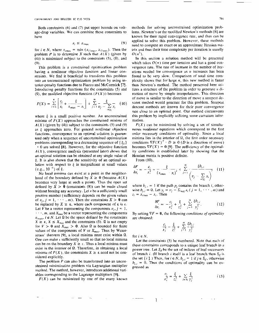
Both constraints (6) and (7) put upper bounds on volt- age-drop variables. We can combine these constraints to have
(9) for i E N , where xima, = min (xilmax, x;~,~,). Then the problem P is to determine X such that A ( X ) (given by (4)) is minimized subject to the constraints ( 5 ) , (8), and (9).
This problem is a constrained optimization problem having a nonlinear objective function and linear con- straints. We find it beneficial to transform this problem into an unconstrained optimization problem by using in- terior-penalty functions due to Fiacco and McCormick [7 ] . Introducing penalty functions for the constraints (5) and (9), the modified objective function ( F ( X ) ) becomes
where 4 is a small positive number. An unconstrained minima of F ( X ) approaches the constrained minima of A ( X ) (given by (4)) subject to the constraints (5) and (9) as 4 approaches zero. For general nonlinear objective functions, convergence to an optimal solution is guaran- teed only when a sequence of unconstrained optimization problems corresponding to a decreasing sequence of { t k } --* 0 are solved [8]. However, for the objective function A ( X ), convergence analysis (presented later) shows that an optimal solution can be obtained at any single value of E. It is also shown that the sensitivity of an optimal so- lution with respect to t is insignificant at small values (e.g., of 4 .
No local minima can exist at a point in the neighbor- hood of the boundary defined by X 2 0 (because A ( X ) becomes very large at such a point). Thus the open set defined by X > 0 (constraints (8)) can be made closed without loosing any accuracy. Let E be a sufficiently small positive number (sufficiency depends on the given values of V j , j = 1, * , m ) . Then the constraints X > 0 can be replaced by X 2 E, where each component of E is E .
Let V be a vector representing the components v j , j = 1, . . . , m , and X,,, be a vector representing the components xima,, i E N . Let Q be the space defined by the constraints X 2 E, X 5 X,,, and the constraints (5). Q is not empty for V > 0 and X,,, > 0. Also Q is bounded for finite values of the components of I/ or X,,,. Thus by Weier- strass' theorem [9], a local minima must exist within Q. One can make E sufficiently small so that no local minima can be on the boundary X 2 E . Thus a local minima must exist in the interior of Q. Therefore, in obtaining a local minima of F ( X ), the constraints X 1 E need not be con- sidered explicitly.
The problem P can also be transformed into an uncon- strained minimization problem via Lagrangian multiplier method. The method, however, introduces additional vari- ables corresponding to the Lagrange multipliers [9].
F ( X ) can be minimized by one of the many known
methods for solving unconstrained optimization prob- lems. Newton's or the modified Newton's methods [8] are known for their rapid convergence rate, and thus can be applied to solve this problem. However, these methods need to compute an exact or an approximate Hessian ma- trix and thus their time complexity per iteration is usually o(n3).
In this section a solution method will be presented which takes U ( n ) time per iteration and has a good con- vergence rate. The rate of increase in the number of iter- ations needed for convergence as n increases has been found to be very slow. Comparison of total time com- plexity shows that for large n, this new method is faster than Newton's method. The method presented here uti- lizes a structure of the problem in order to generate a di- rection of move by simple interpolations. This direction of move is similar to the direction of move a steepest de- scent method would generate for this problem. Steepest descent methods are known for their poor convergence rate close to an optimal point. Our method circumvents this problem by implicitly utilizing some curvature infor- mation.
F ( X ) can be minimized by solving a set of simulta- neous nonlinear equations which correspond to the first order necessary conditions of optimality. Since a local minima lies in the interior of Q , the first order necessary conditions V F ( X ) T - D L: 0 (D is a direction of move) becomes V F ( X ) = 0 [9]. The sufficiency of the optimal- ity conditions is established later by showing that the Hessian matrix is positive definite.
From (lo),
- kJX,) where bJ,l = 1 if the path pJ contains the branch i , other- wise bJ,, = 0. Let yJ = vJ - CIEP, x, ( j = 1 , * . * , m ) and z, = x, - x, . Then
By setting V F = 0, the following conditions of optimality are obtained:
C - 4 tbj,i f = i + c 7 X; Z ; j = l y j
for i E N . Let the constraints (5) be numbered. Note that each of
these constraints corresponds to a unique leaf branch in a power tree. Let S, be the set of indices of leaf successors of branch i . (If branch i itself is a leaf branch then S, is the set { i } .) Then, for i E N , bj,; = 1 i f j E S,, otherwise bj,i = 0. Thus the conditions of optimality can be ex- pressed as
n __ - T

192 IEEE TRANSACTIONS ON COMPUTER-AIDED DESIGN, VOL. 7, NO. 7 , JULY 1988
for i E N . Let S, be the set of indices of immediate suc- cessor (leaf or nonleaf) branches of branch i. (If branch i itself is a leaf branch then Si is the set { i }.) Then a tree structure implies that S, = UjEs, S j f . This relation can be used to rewrite (13) as
for i E N . For our example, these conditions of optimality are
- - - - I - -+5!-- c 5 4 c 4 4 x: 2: - x: 2: x: 2:
5 L 3 = , - - + L - 4 c 2 4 c 4 x: z4 x2 2; x: 2:'
Presently we shall use (13); an application of (14) will be seen later.
Let Y be a vector representing the variables y j ( j = 1, . . . , m ) and Z be a vector representing the variables zi ( i E N ). The constraints ( 5 ) can be rewritten as
n
C bj,;xi + yj = uj (15 ) i = l
f o r j = 1, . *
equations can be rewritten as , m. Let B be the matrix [bj,i]. Then these
B X + Y - V = O . (16)
(17)
Similarly, the constraints (9) can be rewritten as
x + 2 = x;,,, Consider the optimality conditions (13). Only X-vari-
ables occur on the left hand side, and only Y- and Z-vari- ables occur on the right-hand side of these equations. Equating the right-hand members of (13) to ci/( f ?( Y, Z)) , i E N , one obtains
Because the equations in (1 3) are satisfied at the opti- mal point, at this point the variables Y and Z uniquely determine the variables X. This functional dependency can be expressed as X = f ( Y, Z ) where f (Y, Z ) is a vector representing the functions ( Y, Z ), i E N . A nonoptimal point satisfying (16) and (17) cannot satisfy (13), i.e., X f f( Y, 2 ) at such a point.
A solution procedure (denoted by 4 ) will now be pre- sented which starts at a given initial point (XI, Y,, Z , ) satisfying (16) and (17) and terminates at a point satisfy- ing (13), (16), and (17).
The Procedure 4: 1) k = 1. 2) Computef( Yk, zk) by substituting the values of the
Y- and Z-variables (as given by (Yk, zk)) into the right
3) Let ak be the solution to the following line minimi- hand side Of (18) and obtain Dk = f( Yk, 2,) - &.
zation problem:
footnote 4)
subject to 0 I a I a,,,,
minimize F(Xk + aDp, Yk - aBDk, zk - QDk) (See
where a,,, = sup { a : each component of Xk + a D k , Yk
- aBDk and zk - CY Dk is greater than or equal to E } . Let xk+, = Xk + CYkDk, Y k + l = Yk - CYkBDk and zk+, = zk - akDk. IfF(Xk, yk, Zk) - F(Xk+l, yk+l, zk+l ) 5 (a given small positive number) then stop; otherwise replace k by k + 1 and go to step 2.
3. I . Uniqueness of the Optimal Solution
pressed as The objective function F ( X ) (eq. (10)) can also be ex-
" 4 i = I
" 4 i = I
The constraints (16) and (17) are linear. Thus the global optimal solution will be unique if F(X, Y, 2 ) is strictly convex [l]. To show that F(X, Y, 2 ) is strictly convex, it is sufficient to show that V2F(X, Y, Z ) (the Hessian matrix) is positive definite.
It can be seen from (19) that the Hessian matrix is a diagonal matrix (i.e., each of the nondiagonal elements of the matrix is zero). Thus, the eigenvalues of the Hess- ian matrix are its diagonal elements. The diagonal ele- ments are a2F/ax? for i E N , a2F/az? for i E N and a2F/ay,2 f o r j = 1, . , m. Each of these diagonal ele- ments can be seen to be positive (because X > 0, Y > 0 and Z > 0). Thus all eigenvalues are positive and hence F ( X, Y, Z ) is strictly convex and the optimal solution is unique.
3.2. Convergence of the Procedure 4
optimality it is sufficient to show that To show that the procedure 4 converges to the point of
(i) the constraint region is compact, (ii) every iteration results in a reduction in F(X, Y,
(iii) the algorithmic mapping of 4 is closed [9].
Condition i): Step 3 of procedure 4 guarantees that the value of each variable is at least E . Thus, each variable is bounded from below. The variables xi and zi i E N are bounded above by x, (eq. (17)) and the variables yj are bounded above by uj , j = 1, . , m (eq. (16)). Thus, each variable is bounded from above. Since no constraint is a strict inequality, the constrained region is closed, and hence compact.
Condition ii): Let QT = (X', YT, Z T ) be the current point and SQ be the change in Q. F ( Q ) will be reduced if VF( Q) ' SQ is negative and the step size a is suffi- ciently small.
z 1,
4A change aDk in X induces a change -aBDK in Y (eq. (16)) and -aD, in 2 (eq. (17)).
I- . -_

CHOWDHURY AND BREUER: IC P/G NETS 193
With reference to (19),
From (16), 6yj = - Cy= I bj,i6xi and from Thus,
17), SZ; = - 6 ~ ; .
or from the definition of S,,
or using (1 8),
Setting &xi = a ( f; - x i ) (see step 2 of the procedure $)
Each term in the above sum is positive. Thus V F T SQ is a negative quantity. The condition that Q has to be suf- ficiently small is met by the fact that a is determined by a line minimization method. Thus, at every iteration we have a reduction in F ( Q ) .
Condition iii): Let a = 2n + m . The overall procedure $: (E" -+ E " ) can be decomposed into the form $ = ST. Here T: E" -+ E2" is defined by T( Q ) = ( X , Y , 2, D ( X ) , - BD ( X ), - D ( X ) ) giving the initial point and the di- rection of a line search (step 2 of 4). This is followed by the line search S: E2" -+ E" (step 3 of 4). It is known that S is closed if V F ( Q ) # 0 (which indeed is the case if $ is not terminated) [9]. Also, determining D involves computing the functions f (eq. (1 8)) which are continuous in the constrained space. Thus the mapping Tis continu- ous. Therefore, by virtue of the following lemma (see [9] for a proof), the algorithmic mapping $ ( = S T ) is closed.
Lemma 1: Let T w -+ a be a point-to-point mapping and S: a + 0 be a point-to-set mapping. If Tis continuous at X and S is closed on T ( X ), then the composite mapping $ = ST is closed at X .
Since all conditions of convergence are satisfied, the procedure $ converges to the optimal point.
3.3, Comparison with Steepest Descent Direction The steepest descent direction is the negative of the gra-
dient vector. In conjunction with the definition of the function f ( 2 ) (eq. (18)) and ( l l ) , the ith ( i E N ) com- ponent of this direction is
or c;( fi' - x ; )
X:f : . SDDi =
For the procedure $, the corresponding direction is ODi = [ A - x i ] . Thus we have the ratio ODi/SDDi = ( x ; f : ) / ( c i ( f ; + x i ) ) . At points close to the optimal, J; = xi and thus ODi/SDDi = x ? / 2 c i which is
Because of this inherent utilization of the second deriv- ative information, the procedure $ has a convergence rate which is significantly better than that of the steepest de- scent method. However, this second derivative is with re- spect to the objective function of the constrained problem and thus, the convergence rate of the procedure $ is not as good as that of Newton's method.
3.4. Complexity Analysis The procedure $ involves computing f ( Y , Z ) , -BD,
and a. We can compute Fi( Y, 2 ) for i E N from { xj: j E
Si } (eq. (14)). By starting at the leaf nodes and approach- ing toward the root, f(2) can be computed in a single tree traversal, i.e., in O ( n ) time. -BD gives the direc- tion in which Y-variables are changed. Thus, by starting at the root node and accumulating the values ( f; - x i ) for i E N (which are components of D ) in different paths lead- ing to the leaf nodes, -BD can be computed in O( n ) time (see (15)). An iterative method having O ( n ) time com- plexity per iteration can easily be devised for computing a. Thus the overall time complexity of $ is O ( n ) per iteration.
The space complexity for $ can be seen to be 0 ( n ).
[ a2A/ax'] - I .
3.5. Experimental Results Computation Time: Actual p/g distribution systems for
VLSI chips contain from ten to a few hundred branches. Several problems of various sizes (number of branches) were processed on a VAX-750 machine using Fortran-77 programming language. Each problem was separately solved by using the procedure 4, a steepest descent method and a Newton's method. The three methods differ only in computing the direction D (see step 2 of the pro- cedure $). For the steepest descent method, D is taken to be - V F ( Q ) . For Newton's method, D is taken to be - [ V 2 F ( Q ) ] - 'VF( Q ) . The average CPU times required by each of the three methods are listed as a function of n in Table I. Newton's method is inefficient even for small values of n. The procedure $ is about two times faster than the steepest descent direction for all values of n.
Sensitivity to 4: The following table shows a typical example of variations of the optimal solution with respect to the value of E . It can be seen that the sensitivity of the optimal solution with respect to is insignificant for the values of 4 listed here.
IV. POWER/GROUND (p/g ) TOPOLOGY SELECTION FOR
Given a topology for a power/ground tree, the proce- dure $ provides the area requirement for the topology. Thus the procedure can be employed to compare different topologies in terms of area requirements. This section considers the case of regular cells placed in rows and col- umns. Gate array design style gives rise to this kind of
ARRAY OF REGULAR CELLS

TABLE I RUN TIME IN SECONDS
1.2 6.1
50.3
3.2 421.5
I 128 I 6.8 I 64
21.4
3.2 8.2 421.5
I 32 I 1.6 I
E
0.001
3.7
value of the optimal solution
24237
0 . m 1
0.000001
1 1.5: 1 17.7 1 47.6 1 1 37.0 107.2
1024 94.8 235.6
24172
24 167
24186 I l l
24163 I l l placement. The effect of variation in certain parameters, such as current, voltage drop, number of rows ( R ) , num- ber of columns ( C ), number of pads ( P ) , and pad posi- tion on the total area of the power (ground) routes will be studied. It is assumed that there is only one power pin and only one ground pin per cell (see Fig. 3). For simplicity both the horizontal and vertical spacing between centers of adjacent cells are assumed to be the same. Let L be this spacing. All cells are assumed to draw the same current and the maximum allowable voltage drop between the power (ground) pad and each power (ground) pin is bounded by up ( vg>.
The following are some experimental results regarding the variation of area with respect to current per pin, volt- age drop, and spacing ( L ) .
Area increases linearly with current per pin except at very low values of the current, where area remains con- stant due to the minimum line width constraint. Area is inversely proportional to up ( u s ) . However, for high val- ues of up ( U , ) , the area again remains constant due again to the constraint of minimum line width. Area is propor- tional to Lp, where p is around 1 for small values of L, and increases as L increases. For large values of L, p is around 2. The linear variation at small values for L is again due to the constraint of minimum line width.
m:::h7
Fig. 3. Normal scheme of routing for regular cells.
794 IEEE TRANSACTIONS ON COMPUTER-AIDED DESIGN, VOL 7. NO. I. JULY 1988
Number of Row (R): As seen in Fig. 4, area is propor- tional to R P , where p is about 1 for small values of C and gets larger as C increases. Keeping in mind that the area being investigated is for a tree shown in Fig. 3, since p is always greater than 1, to minimize the area, a pad should be placed such that if R = 2m, then separate sub- trees should supply power to m rows which are above and below the pad.
Number of Pads (P): We assume that P divides R , and that each pad supplies power to R I P rows. Sincep is about 1 for small values of C, a reduction in area by having more than one pad is significant only for large values of C. Also, the rate of reduction in area decreases consid- erably as P is increased (Fig. 5 ) . The analysis does not include pad area. Ratio of R and C: It appears that for N cells placed in
R rows and C columns, the area is minimal when R = 2C (see Fig. 6). However, while the reduction in area due to a unit increase in R is large for R C 2C, the increase in area is small for a unit increase in R when R > 2C. Thus R can be selected from a wide range of values with little impact on area. The reason for the very large increase in area for low values of R is that for these cases only a small fraction of the total number of pins can be supplied at the full allowable voltage drop.
Normal versus Star: Two schemes for routing regular arrays have been employed by chip designers. In the “star” scheme (Fig. 7), each pin is supplied from the pad by an individual route. The “normal” scheme is shown in Fig. 3.
For a regular array of cells, let A,, be the area of a nor- mal tree and A, be that for a star tree, including the area due to spacing between adjacent routes. Fig. 8 shows the plot of A , / A , as a function of L and current per pin. Ex- perimentally we have found that the star scheme of rout- ing requires less area than the normal scheme of routing when ( Z L / v ) exceeds some constant K , where U is equal to up ( U , ) for a power (ground) tree. K depends on the values of R and C. For a 16 X 16 array, K is found to be about 26 mho-p ( p is assumed to be 0.03/square and the maximum current density is assumed to be 1 mA/p) . For a 1 cm X 1 cm chip consisting of this array, L is about 600 p . For this chip K > 26 can be achieved for values of I about 4.5 mA and v = 100 mV.
The possible saving in area in star scheme of routing is

CHOWDHURY AND BREUER: IC P/G NETS 195
AN/AS A
I = 10 ma I = 5 ma
I = 1 ma 1.0 ’ I
1 2 3 4 5 6 1
Fig. 4. Variation of area with respect to R.
AREA
T c.10
1 2 3 4 5 6 7 8 Fig. 5. Variation of area with respect to P .
AREA
5 1 c 10 20 30 40 50
Fig. 6 . Variation of area with respect to the ratio of R to C .
I ***I
I -1 L
... riJ Fig. 7. Star scheme of routing for regular cells.
L L Fig. 8. Ratio of area for star and normal schemes of routing
due to the fact that the voltage drop in each individual routes can attain the maximum allowable limit, unless re- stricted by minimum width or metal migration con- straints. This is not true in the case of the normal scheme of routing. The maximum allowable voltage drop can ex- ists between the pad and the pins at the farthest ends only. The star scheme of routing does not always lead to less total area because of the spacing between the adjacent routes. This scheme becomes better than the normal scheme when the voltage drop (and not the minimum width or metal migration) constraints become predomi- nant factor in determining the widths of the routes. An additional advantage of the star scheme is that it helps in isolating noise in individual p/g routes.
Analytical Study of the Ratio A, /A,: It was shown ear- lier that A,, = c ,ILp/v , where c1 is a constant of propor- tionality and 1 I p 5 2. Assume that L is sufficiently large so that p = 2.
The area of a star is composed of two components:
1) Area due to the p/g routes; 2) Area due to spacing between adjacent routes.
Component (1) is proportional to ZL2/ v while compo- nent (2) is proportional to L . Thus A, = c21L2/v + c3L where c2 and c3 are constants of proportionality.
We define the ratio
and thus,
CIC3 Iv _ - - dR dL (c2IL + c 3 v y .
From this equation we see that.R increases with L . For very large L, c2 IL >> c3 U . Then d R / d L = cIc3 v / c 2 IL2. Thus d R / d L tends to be 0 as L tends to be very large. For a constant R ( = k ) we can write c1 ZL = k [ c2ZL + c3 U ]
from which one obtains I L / v = k c 3 / [ c I - kc2] which is a constant. Our experimental model verified these results.
V. CONCLUSION We have presented an algorithm for determining the
width of power and ground routes such that certain rele- vant constraints are satisfied and the resulting routing area is minimized. This algorithm should eliminate the need

796 IEEE TRANSACTIONS ON COMPUTER-AIDED DESIGN, VOL 7, NO. 7. JULY 1988
for the manual computation currently used to ensure that these constraints are satisfied, as well as lead to reduced chip area. The algorithm is applicable to multilayer schemes for power and ground routing, with little or no modification. Some of the case studies indicate results which to some are rather counter intuitive. They point out unconventional design methods, such as the star scheme for routing, which some designers have already found to be of value.
REFERENCES
S. Chowdhury (M’86) received the B.S. degree in electrical engineering from the University of Chittagong, Bangladesh in 1978, the M.S. degree in electrical communication engineering from the Indian Institute of Science, Bangalore, India in 1981, and the Ph.D. degree in electrical engi- neering from the University of Southern Califor- nia, Los Angeles, in 1986.
Presently he is an Assistant Professor in the Electrical and Computer Engineering Department of the University of Iowa, Iowa City. In 1987 he
received a best paper award from Design Automation Conference and a National Science Foundation Initiation Award. His research interests in- clude computer aided design, VLSI circuits and mathematical optimiza-
*
tion. M. S. Bazaraa and C. M. Shetty, Nonlinear Programming. New York: Wiley, 1979. J. R. Black, “Electromigration failure modes in aluminium metali- zation for semiconductor devices,” Proc. IEEE, vol. 57, pp. 1587- 1594, Sept. 1969. S. Chowdhury, “An automated design of minimum-area IC power/ ground nets,” in Proc. 24th DA Conf., pp. 223-229, June 1987. S. Chowdhury and M. A. Breuer, “The construction of minimal area power and ground nets for VLSI circuits,” in Proc. 22nd DA Conf., pp, 794-797, June 1985. S . Chowdhury and M. A. Breuer, “Minimal area sizing of power and ground nets for VLSI circuits,” in Proc. 4th MIT Conf. on Advanced Research in VLSI, Apr. 1986. Melvin A. Breuer (S’58-M’65-SM’73-F’85) re- F. M. D’Heurle, “Electromigration and failure in electronics: An in- ceived the B.S. (with honors) and M.S. degrees troduction,” Proc. IEEE, vol. 59, pp. 1409-1418, Oct. 1971. in engineering from the University of California, A. V. Fiacco and G . P. McCormick, Nonlinear Programming: Se- Los Angeles, in 1959 and 1961, respectively, and quential Unconstrained Minimization Techniques. New York: the Ph.D. degree in electrical engineering from Wiley, 1968. the University of California, Berkeley, in 1965. R. Fletcher, Practical Methods of Optimization-Vol. 2. New York: He then joined the staff of the Electrical Engi- Wiley, 1981. neering Department of the USC Los Angeles, D. G . Luenberger, Introduction to Linear and Nonlinear Program- where he is currently a Professor of both electrical ming. Reading, MA: Addison-Wesley, 1973. engineering and computer science. His main in- C. Mead and L. Conway, Introduction to VLSI Systems. Reading, terests are in the area of switching theory, com- MA: Addison-Wesley, Oct. 1980. puter aided design of computers, fault tolerant computing, VLSI circuits. A. S. Moulton, “Laying the power and ground wires on a VLSI chip,” He was a Fullbright-Hays Scholar in 1973. He is the editor and co-author in Proc. 20th DA Conf., pp. 754-755, July 1983. of Design Automation of Digital Systems: Theory and Techniques, Pren- B. T. Preas and P. G. Karger, “Automatic placement: A review of tice-Hall; editor of Digital Systems Design Automation: Languages, Sim- current techniaues,” in Proc. 23rd DA Conf., PP. 622-629, 1986. ulation and Data Base. ComDuter Science Press; co-author of Diaanosis
D,., Chowdhury i s a member of K~~~~ N ~ ,
1131 H-J. Rothemel and D. A. Mlynski, “Cokpuiation of power and ground supply nets in VLSI layout,” in Proc. 18th DA Conf., pp. 37- 47, 1981.
[I41 W. S. Song and L. A. Glasser, “Power distribution techniques for VLSI circuits,” IEEE Solid-State Circuits, vol. SC-Feb. 1986.
[I51 Z . A. Syed and A. El Gamal, “Single layer routing of power and ground networks in integrated circuits,” J. Digital Syst., vol. 6 , no. 1 , pp. 53-63, 1982.
and Reliable Design of Digital Systems, Computer Science Press, and co- editor of Computer Hardware Description Languages and their Applica- tions, North-Holland. He has published over 100 technical papers and was formerly the editor-in-chief of the Journal of Design Automation and Fault Tolerant Computing, the co-editor of the Journal of Digital Systems, and was the Program Chairman of the Fifth Int’l IFlP Conference on Computer Hardware Description Languages and Their Applications.
Dr. Breuer is a member of Sigma Xi, Tau Beta Pi, Eta Kappa NU.