Bipolar Junction Transistors (BJTs) - Microelectronic Circuits ...
Upload
khangminh22Category
view
0download
0
Calhoun: The NPS Institutional Archive
DSpace Repository
Theses and Dissertations 1. Thesis and Dissertation Collection, all items
2019-12
OPTIMIZATION OF MULTI-JUNCTION SOLAR
CELL FOR SPACE APPLICATIONS MODELED
WITH RUBY, MATLAB, AND SILVACO
Allen, Tony Jr.
Monterey, CA; Naval Postgraduate School
http://hdl.handle.net/10945/64137
Downloaded from NPS Archive: Calhoun

NAVAL POSTGRADUATE
SCHOOLMONTEREY, CALIFORNIA
THESIS
OPTIMIZATION OF MULTI-JUNCTION SOLAR CELL FOR SPACE APPLICATIONS MODELED WITH RUBY,
MATLAB, AND SILVACO
by
Tony Allen Jr.
December 2019
Thesis Advisor: Sherif N. Michael Second Reader: Matthew A. Porter
Approved for public release. Distribution is unlimited.

THIS PAGE INTENTIONALLY LEFT BLANK

REPORT DOCUMENTATION PAGE Form Approved OMB No. 0704-0188
Public reporting burden for this collection of information is estimated to average 1 hour per response, including the time for reviewing instruction, searching existing data sources, gathering and maintaining the data needed, and completing and reviewing the collection of information. Send comments regarding this burden estimate or any other aspect of this collection of information, including suggestions for reducing this burden, to Washington headquarters Services, Directorate for Information Operations and Reports, 1215 Jefferson Davis Highway, Suite 1204, Arlington, VA 22202-4302, and to the Office of Management and Budget, Paperwork Reduction Project (0704-0188) Washington, DC 20503.
1. AGENCY USE ONLY(Leave blank)
2. REPORT DATEDecember 2019
3. REPORT TYPE AND DATES COVEREDMaster's thesis
4. TITLE AND SUBTITLEOPTIMIZATION OF MULTI-JUNCTION SOLAR CELL FOR SPACEAPPLICATIONS MODELED WITH RUBY, MATLAB, AND SILVACO
5. FUNDING NUMBERS
6. AUTHOR(S) Tony Allen Jr.
7. PERFORMING ORGANIZATION NAME(S) AND ADDRESS(ES)Naval Postgraduate SchoolMonterey, CA 93943-5000
8. PERFORMINGORGANIZATION REPORTNUMBER
9. SPONSORING / MONITORING AGENCY NAME(S) ANDADDRESS(ES)N/A
10. SPONSORING /MONITORING AGENCYREPORT NUMBER
11. SUPPLEMENTARY NOTES The views expressed in this thesis are those of the author and do not reflect theofficial policy or position of the Department of Defense or the U.S. Government.
12a. DISTRIBUTION / AVAILABILITY STATEMENT Approved for public release. Distribution is unlimited.
12b. DISTRIBUTION CODE A
13. ABSTRACT (maximum 200 words)The purpose of this research is to document further research into the optimization techniques
investigated by James Walsh and applied to Multi-junction Solar Cells. Walsh performed his research with the Near Orthogonal Latin Hypercube (NOLH) in order to optimize the design specifications for each layer of solar cell thickness and doping concentration. Walsh at the same time evaluated cell performance under the radiation effects of the space environment. This research performed a similar analysis, except for the radiation effects, but focused more on producing an algorithm that could be executed from single user input and significantly reducing the selected design space. This research produced an efficient program that seamlessly operates between Ruby, MATLAB, and Silvaco ATLAS in order to produce an optimal designed dual-junction solar cell for space applications, in a much smaller design space than the technique utilized by Walsh.
14. SUBJECT TERMSspace solar cells, radiation effects, photovoltaic modeling, efficiency, optimization
15. NUMBER OFPAGES
10716. PRICE CODE
17. SECURITYCLASSIFICATION OFREPORTUnclassified
18. SECURITYCLASSIFICATION OF THISPAGEUnclassified
19. SECURITYCLASSIFICATION OFABSTRACTUnclassified
20. LIMITATION OFABSTRACT
UU
NSN 7540-01-280-5500 Standard Form 298 (Rev. 2-89) Prescribed by ANSI Std. 239-18
i

THIS PAGE INTENTIONALLY LEFT BLANK
ii

Approved for public release. Distribution is unlimited.
OPTIMIZATION OF MULTI-JUNCTION SOLAR CELL FOR SPACE APPLICATIONS MODELED WITH RUBY, MATLAB, AND SILVACO
Tony Allen Jr. Captain, United States Marine Corps
BSEE, University of North Florida, 2013
Submitted in partial fulfillment of the requirements for the degree of
MASTER OF SCIENCE IN ELECTRICAL ENGINEERING
from the
NAVAL POSTGRADUATE SCHOOL December 2019
Approved by: Sherif N. Michael Advisor
Matthew A. Porter Second Reader
Douglas J. Fouts Chair, Department of Electrical and Computer Engineering
iii

THIS PAGE INTENTIONALLY LEFT BLANK
iv

ABSTRACT
The purpose of this research is to document further research into the optimization
techniques investigated by James Walsh and applied to Multi-junction Solar Cells. Walsh
performed his research with the Near Orthogonal Latin Hypercube (NOLH) in order to
optimize the design specifications for each layer of solar cell thickness and doping
concentration. Walsh at the same time evaluated cell performance under the radiation
effects of the space environment. This research performed a similar analysis, except for
the radiation effects, but focused more on producing an algorithm that could be executed
from single user input and significantly reducing the selected design space. This research
produced an efficient program that seamlessly operates between Ruby, MATLAB, and
Silvaco ATLAS in order to produce an optimal designed dual-junction solar cell for
space applications, in a much smaller design space than the technique utilized by Walsh.
v

THIS PAGE INTENTIONALLY LEFT BLANK
vi

vii
TABLE OF CONTENTS
I. INTRODUCTION..................................................................................................1 A. SOLAR CELLS FOR SPACE APPLICATIONS ...................................1 B. PAST WORK AT NPS ..............................................................................1 C. OBJECTIVE ..............................................................................................2 D. ORGANIZATION .....................................................................................2
II. BACKGROUND ....................................................................................................3 A. SEMICONDUCTORS ...............................................................................3
1. Energy Bands and Charge Carriers .............................................3 2. Semiconductor Materials and Doping Concentrations ..............7 3. PN Junction ....................................................................................8 4. Generation Rate and Recombination .........................................11
B. SOLAR CELLS ........................................................................................12 1. Photodetectors and Photoconductors .........................................12 2. Solar Cell Operation ....................................................................14
C. MULTI-JUNCTION SOLAR CELLS ...................................................15 1. Manufacturing..............................................................................15 2. Tunnel Junctions ..........................................................................15
III. METHODOLOGY ..............................................................................................19 A. MODELED CELL ...................................................................................19 B. SILVACO ATLAS ...................................................................................21 C. MOBILITY ...............................................................................................23 D. NEARLY ORTHOGONAL LATIN HYPERCUBE ............................23
IV. RESULTS .............................................................................................................25 A. MODELED CELL ...................................................................................25 B. OPTIMIZATION RESULTS .................................................................26

viii
V. CONCLUSIONS AND FUTURE WORK .........................................................29
APPENDIX A. RUBY DOWNLOAD AND FAMILIARIZATION ..................31
APPENDIX B. INP PARAMETER FUNCTION................................................35
APPENDIX C. GAP PARAMETER FUNCTION ..............................................37
APPENDIX D. GAAS PARAMETER FUNCTION ...........................................39
APPENDIX E. ALAS PARAMETER FUNCTION ............................................41
APPENDIX F. ALAS MOBILITY FUNCTION .................................................43
APPENDIX G. GAAS MOBILITY FUNCTION ................................................45
APPENDIX H. GAP MOBILITY FUNCTION ...................................................47
APPENDIX I. INP MOBILITY FUNCTION ....................................................49
APPENDIX J. INGAP WINDOW MOBILITY FUNCTION ...........................51
APPENDIX K. INGAP EMITTER MOBILITY FUNCTION ..........................53
APPENDIX L. INGAP BASE MOBILITY FUNCTION ...................................55
APPENDIX M. INALGAP WINDOW MOBILITY FUNCTION .....................57
APPENDIX N. INALGAP BSF MOBILITY FUNCTION.................................59
APPENDIX O. ALGAP WINDOW PARAMETER FUNCTION .....................61
APPENDIX P. ALGAAS MOBILITY FUNCTION ...........................................63
APPENDIX Q. CREATE DESIGN SPACE VECTOR ......................................65
APPENDIX R. CREATE DESIGN SPACE FROM RUBY ...............................67
APPENDIX S. CREATE DATA VECTORS FROM .LOG FILE ....................69

ix
APPENDIX T. READ DATA FROM .LOG FILE .............................................71
APPENDIX U. CREATE Η, VOC, JSC, & FF FROM .LOG FILE........................73
APPENDIX V. CREATING DECKBUILD FILES ............................................75
APPENDIX W. MODEL DECKBUILD FILE .....................................................79
APPENDIX X. MATLAB EXECUTES DECKBUILD ......................................81
APPENDIX Y. CURVE FITTING AND PROBABILITY ANALYSIS............83
LIST OF REFERENCES ................................................................................................85
INITIAL DISTRIBUTION LIST ...................................................................................87

x
THIS PAGE INTENTIONALLY LEFT BLANK

xi
LIST OF FIGURES
Figure 1. Bandgap structure for a semiconductor material. Source: [1]. ....................3
Figure 2. Direct and Indirect electron transitions in semiconductors. Source: [5]. ................................................................................................................4
Figure 3. Real band diagram for Si and GaAs. Source: [5]. ........................................5
Figure 4. Intrinsic carrier concentration. Source: [5]. .................................................5
Figure 5. Filled states and Fermi-levels. Source: [6]. .................................................6
Figure 6. Intrinsic Si with no impurity. Source: [7]. ...................................................7
Figure 7. Silicon donor doped samples. Source: [7]. ..................................................8
Figure 8. Silicon acceptor doped samples. Source: [7]. ..............................................8
Figure 9. PN junction band diagram. Source: [6]........................................................9
Figure 10. PN junction. Source: [5]. ...........................................................................10
Figure 11. Light generating electron-hole pairs. Source: [6]. .....................................11
Figure 12. Electron promoted to conduction band. Source: [1]. .................................12
Figure 13. Solar Spectrum for AM0 and AM1.5. Source: [7].....................................13
Figure 14. I-V characteristics for solar cell. ................................................................15
Figure 15. Static I-V characteristics of a tunnel diode. Source: [7]. ...........................16
Figure 16. Three components of static characteristics. Source: [7]. ...........................17
Figure 17. Modeled cell profile. Source: [8]. ..............................................................19
Figure 18. I-V measurements under AM0 and AM1.5G. Source: [8].........................21
Figure 19. Modeled cell created in Silvaco .................................................................22
Figure 20. Comparison of real and modeled cell. Source: [8]. ...................................25
Figure 21. Comparison of model and optimization passes .........................................27
Figure 22. A-1: Find Ruby Download. Source: [10]. ..................................................31

xii
Figure 23. A-2: Identify Ruby download for your device. Source: [10]. ....................31
Figure 24. A-3: Ruby installer. Source: [10]. ..............................................................32
Figure 25. A-4: NOLHS Commands. Source: [10]. ....................................................32
Figure 26. A-5: Help Command Results for stack_nolhs.rb. Source: [10]. ................33

xiii
LIST OF TABLES
Table 1. Lighted current voltage for GaAs. Source: [8]. .........................................20
Table 2. NOLH example ..........................................................................................24
Table 3. Performance comparison of real and modeled cells ..................................26
Table 4. Optimization results ...................................................................................27
Table 5. Model vs. optimization improvements ......................................................28
Table 6. Optimal designed dual-junction cell ..........................................................28

xiv
THIS PAGE INTENTIONALLY LEFT BLANK

xv
LIST OF ACRONYMS AND ABBREVIATIONS
AlAs aluminum arsenide AlGaAs aluminum gallium arsenide AlInP aluminum indium phosphide AlP aluminum phosphide GaP gallium phosphide Ge germanium GA genetic algorithm GaAs gallium arsenide InAlGaP indium aluminum gallium phosphide InGaP indium gallium phosphate InP indium phosphide NOLH nearly orthogonal Latin hypercube NPS Naval Postgraduate School NREL National Renewable Energy Laboratory

xvi
THIS PAGE INTENTIONALLY LEFT BLANK

xvii
ACKNOWLEDGMENTS
I would like to show appreciation for the Naval Postgraduate School staff members
who helped me in my research efforts: my thesis advisor, Professor Sherif Michael, my
second reader, Matthew Porter, and Susan Sanchez from the Department of Operations
Research.
I would also like to thank my wife, Latoya, my children, Essence, Elisha, and Tony,
and my mother-in-law, Angela, for their support and patience during this time.

xviii
THIS PAGE INTENTIONALLY LEFT BLANK
1
I. INTRODUCTION
A. SOLAR CELLS FOR SPACE APPLICATIONS
Power sources for space craft may include batteries, both electric and chemically
fueled engines, and photovoltaic systems onboard the craft. It is necessary for the design
of these systems to be dependable and capable of surviving the harsh environment of space.
Photovoltaic systems, or solar cells, have proven to be dependable in supplying spacecraft
systems with the power they require. The cost of producing state-of-the-art multi-junction
solar cells usually prohibits their use for terrestrial applications; however, multi-junction
solar cells are vital for the survivability and success of space systems. For space
applications, higher-cost multi-junction solar cells are preferred over the cheaper terrestrial
solar cell variants due to their ability to withstand the harsh environment of space.
Additionally, improving the efficiency in solar panel design will result in less of an
electrical load required for solar power generation, a reduced surface area to prevent
collision with orbital debris, and improve the capability to meet higher power demands.
The inspection of solar cell characteristics such as doping concentrations and
material thicknesses make designing optimal cell parameters an immense task. The
utilization of complex computer software that executes numerical approximation in order
to solve nonlinear sets of differential equations while simultaneously modeling solar cell
operation, are fundamental towards simulating the efficiency of theorized solar cell designs
with precise parameters. Design improvements can be achieved by simulating solar cells
with variants of the parameters listed above. Inspecting large numbers of simulation results
provides a better observation of what parameter values result in the highest efficiency of
the respective cell at a fraction of the cost of manufacturing countless solar cells with
different characteristics.
B. PAST WORK AT NPS
Numerous theses have researched solar cell optimization at the Naval Postgraduate
School (NPS). James Walsh [1] successfully modeled and simulated radiation effects on
dual-junction cells under AM0 conditions. Panayiotis Michalopoulos [2] successfully
2
implemented the modeling of several solar cells using Silvaco ATLAS (Silvaco), by
demonstrating the performance of modeled cells and tested cells while studying their
individual solar cell efficiency. Finally, both Raymond Kilway [3] and Silvio Pueschel [4]
continued the work of P. Michalopoulos by researching the ability to optimize solar cell
design by performing either a genetic algorithm (GA) or nearly orthogonal Latin
hypercubes (NOLH), respectively. NOLH proved to be the more efficient method due to
the length of time required to derive an optimized design and remains the method executed
during the conduct of the research described here.
C. OBJECTIVE
The goal of this research is to inspect the solution space derived from the NOLH.
J. Walsh investigated a solution space of more than 2,000 points for thicknesses and doping
concentrations, discussed later in Chapter III. First, the published results of a simulated and
manufactured dual-junction solar cell was utilized to derive the respective thicknesses and
doping concentrations as the model for this research. Next, parameters were precisely
determined to produce a scalable and realistic design space focusing mainly on the
thicknesses and doping concentrations for the respective layers present in the dual-junction
cell. Finally, parameters for binary, ternary, and quaternary materials were heavily utilized
and calculated with MATLAB for use for the final design simulated in Silvaco ATLAS.
To discuss the modeled solar cell researched more in depth, this research will converse a
dual-junction indium gallium phosphate (InGaP)/gallium arsenide (GaAs) cell fabricated
and tested at The Ohio State University [4]. This dual-junction solar cell provides tangible
results to compare the produced simulated results.
D. ORGANIZATION
In Chapter II, the physics of semiconductors, solar cells, and multi-junction solar
cells will be discussed. Chapter III will discuss the methodology of research and
optimization techniques utilized with Silvaco ATLAS, MATLAB, and the NOLH
algorithm. Chapter IV will discuss and list the results of the simulation presented
throughout this research. Finally, Chapter V will discuss the conclusion, areas of future
improvements, and recommended future work.
3
II. BACKGROUND
A. SEMICONDUCTORS
Semiconductor optimal performance is achieved only when the respective material
can be grown with a high fidelity of crystallinity, while at the same time the impurities and
defects can be regulated. In order to maintain exceptional structural attributes in the
semiconductor design, a high-quality substrate must be available. Consequently, this
requires growing crystals in bulk, which are then sliced and polished to allow epitaxial
growth of thin regions within the semiconductor including heterostructures.
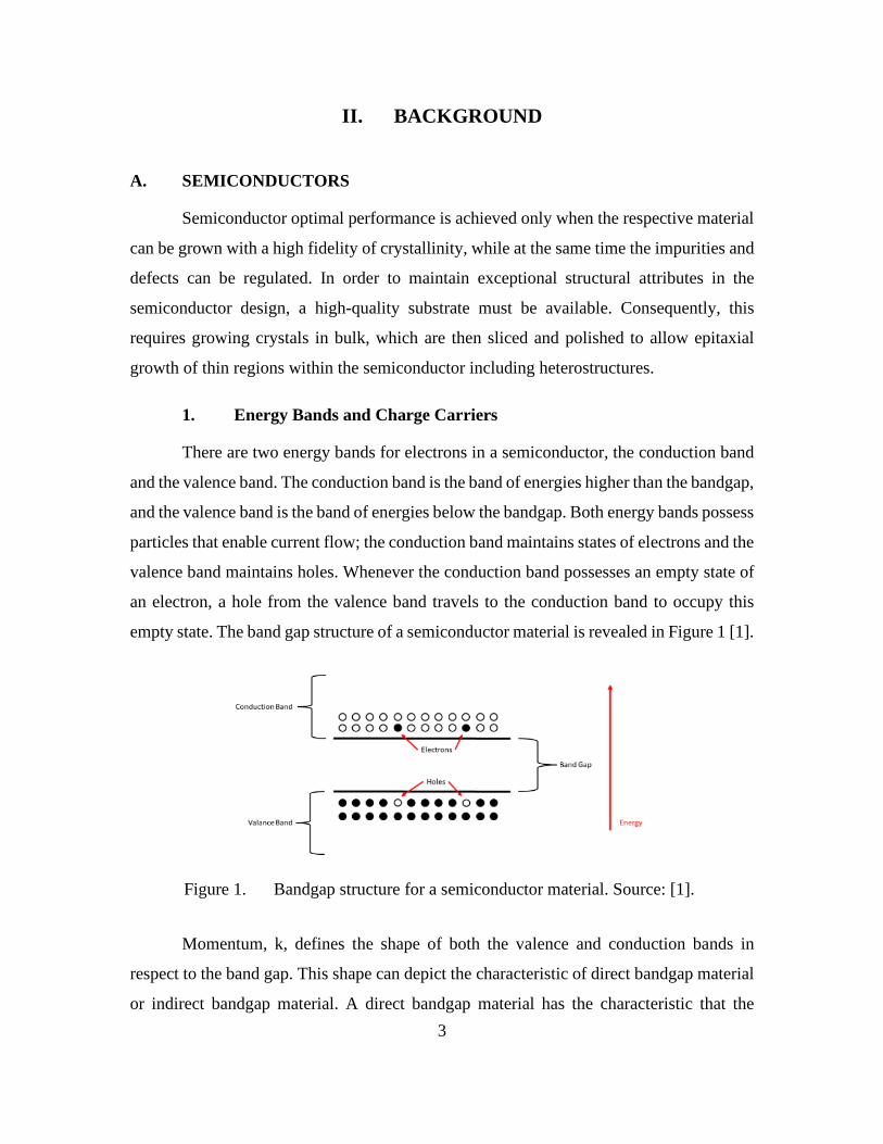
1. Energy Bands and Charge Carriers
There are two energy bands for electrons in a semiconductor, the conduction band
and the valence band. The conduction band is the band of energies higher than the bandgap,
and the valence band is the band of energies below the bandgap. Both energy bands possess
particles that enable current flow; the conduction band maintains states of electrons and the
valence band maintains holes. Whenever the conduction band possesses an empty state of
an electron, a hole from the valence band travels to the conduction band to occupy this
empty state. The band gap structure of a semiconductor material is revealed in Figure 1 [1].
Figure 1. Bandgap structure for a semiconductor material. Source: [1].
Momentum, k, defines the shape of both the valence and conduction bands in
respect to the band gap. This shape can depict the characteristic of direct bandgap material
or indirect bandgap material. A direct bandgap material has the characteristic that the
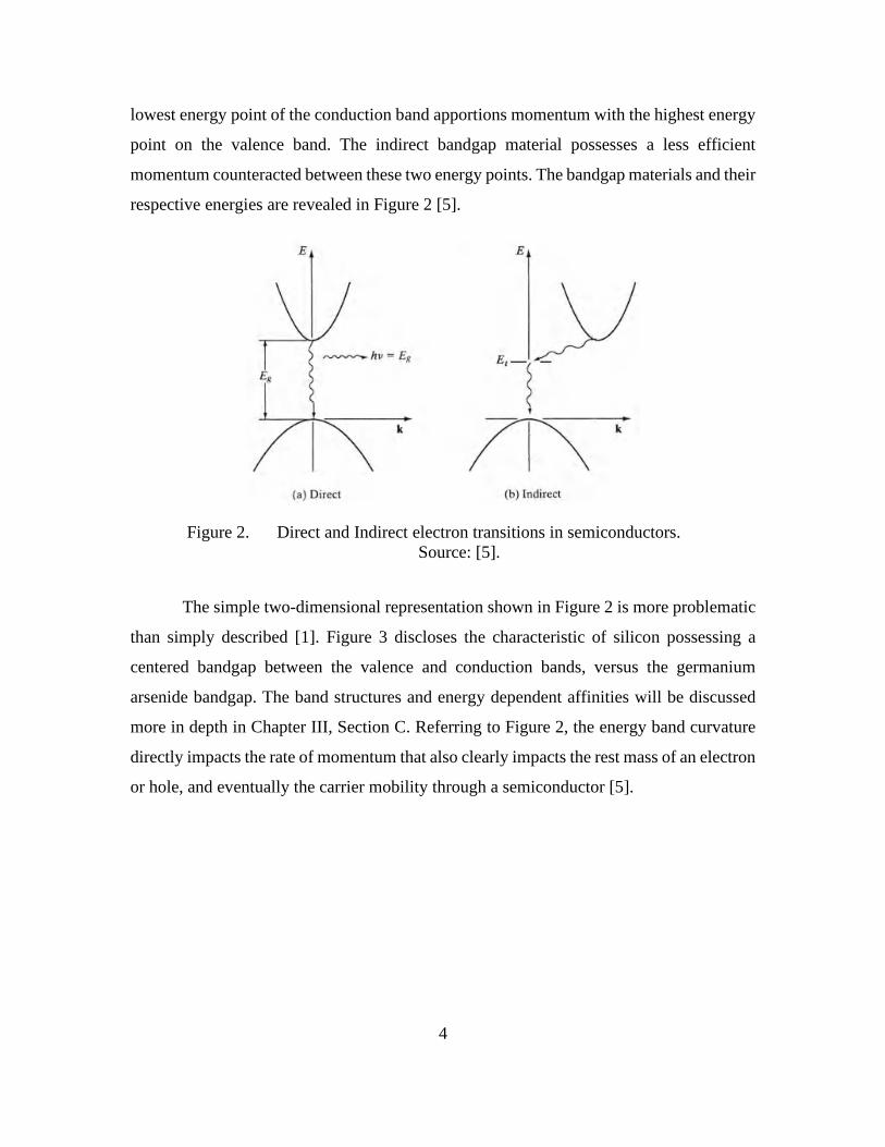
4
lowest energy point of the conduction band apportions momentum with the highest energy
point on the valence band. The indirect bandgap material possesses a less efficient
momentum counteracted between these two energy points. The bandgap materials and their
respective energies are revealed in Figure 2 [5].
Figure 2. Direct and Indirect electron transitions in semiconductors. Source: [5].
The simple two-dimensional representation shown in Figure 2 is more problematic
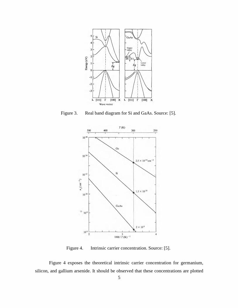
than simply described [1]. Figure 3 discloses the characteristic of silicon possessing a
centered bandgap between the valence and conduction bands, versus the germanium
arsenide bandgap. The band structures and energy dependent affinities will be discussed
more in depth in Chapter III, Section C. Referring to Figure 2, the energy band curvature
directly impacts the rate of momentum that also clearly impacts the rest mass of an electron
or hole, and eventually the carrier mobility through a semiconductor [5].
5
Figure 3. Real band diagram for Si and GaAs. Source: [5].
Figure 4. Intrinsic carrier concentration. Source: [5].
Figure 4 exposes the theoretical intrinsic carrier concentration for germanium,
silicon, and gallium arsenide. It should be observed that these concentrations are plotted
6
as a function of inverse temperature and room temperature values are indicated for
reference. The intrinsic concentration can be calculated simply by the product of both the
electron concentration 𝑛𝑛𝑜𝑜, and hole concentration 𝑝𝑝𝑜𝑜, of a material. This is revealed in
Equation (1) [5].
𝑛𝑛𝑜𝑜 𝑝𝑝𝑜𝑜 = 𝑛𝑛𝑖𝑖2 (1)
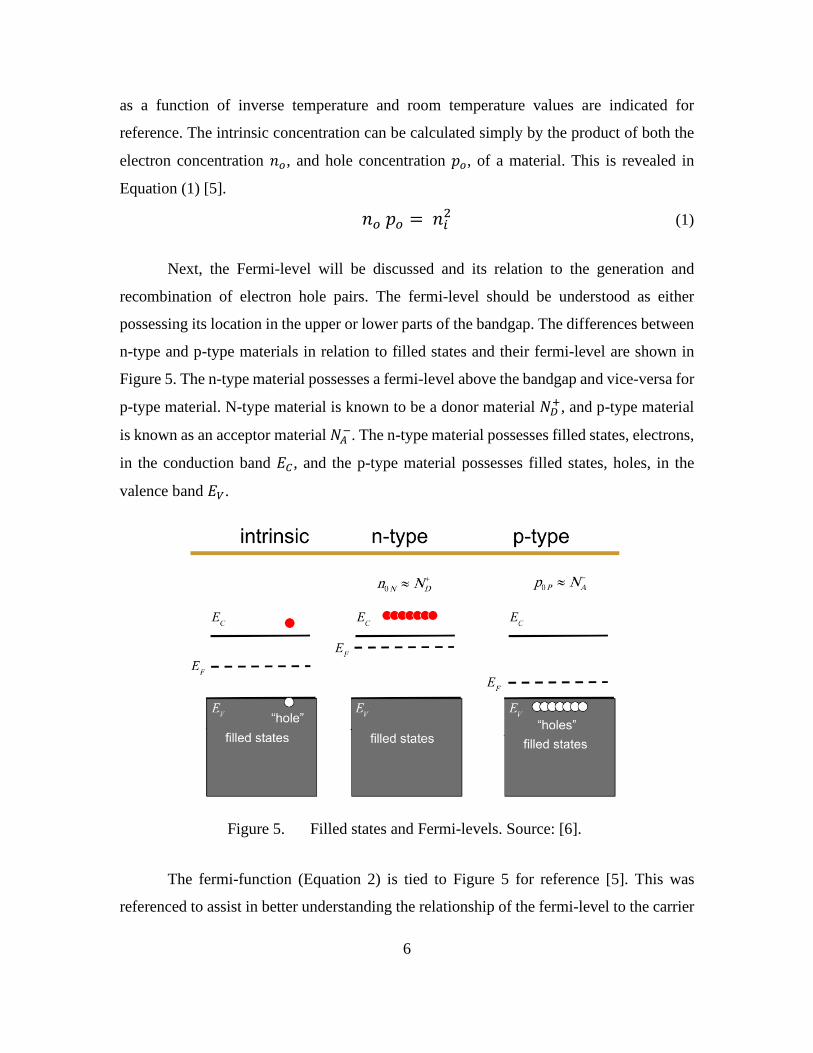
Next, the Fermi-level will be discussed and its relation to the generation and
recombination of electron hole pairs. The fermi-level should be understood as either
possessing its location in the upper or lower parts of the bandgap. The differences between
n-type and p-type materials in relation to filled states and their fermi-level are shown in
Figure 5. The n-type material possesses a fermi-level above the bandgap and vice-versa for
p-type material. N-type material is known to be a donor material 𝑁𝑁𝐷𝐷+, and p-type material
is known as an acceptor material 𝑁𝑁𝐴𝐴−. The n-type material possesses filled states, electrons,
in the conduction band 𝐸𝐸𝐶𝐶, and the p-type material possesses filled states, holes, in the
valence band 𝐸𝐸𝑉𝑉.
Figure 5. Filled states and Fermi-levels. Source: [6].
The fermi-function (Equation 2) is tied to Figure 5 for reference [5]. This was
referenced to assist in better understanding the relationship of the fermi-level to the carrier
7
concentrations present in the p-type or n-type specific materials. These n-type and p-type
materials are the building blocks for PN junction semiconductors and will be discussed in
the next paragraph.
𝑓𝑓(𝐸𝐸) = 11+ 𝑒𝑒(𝐸𝐸−𝐸𝐸𝐹𝐹)/𝑘𝑘𝑘𝑘 (2)
𝑛𝑛 = 𝑁𝑁𝐷𝐷𝑒𝑒(𝐸𝐸𝐹𝐹− 𝐸𝐸𝐶𝐶)/𝑘𝑘𝑘𝑘 (3)
𝑝𝑝 = 𝑁𝑁𝐴𝐴𝑒𝑒(𝐸𝐸𝑉𝑉− 𝐸𝐸𝐹𝐹)/𝑘𝑘𝑘𝑘 (4)
Equations (3) and (4) reveal the relationships that are shared between the fermi-
levels, electron carrier concentration, and hole concentrations of the material and how the
fermi-level directly impacts both carriers [5].
2. Semiconductor Materials and Doping Concentrations
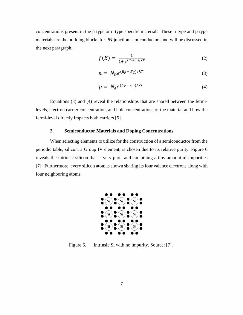
When selecting elements to utilize for the construction of a semiconductor from the
periodic table, silicon, a Group IV element, is chosen due to its relative purity. Figure 6
reveals the intrinsic silicon that is very pure, and containing a tiny amount of impurities
[7]. Furthermore, every silicon atom is shown sharing its four valence electrons along with
four neighboring atoms.
Figure 6. Intrinsic Si with no impurity. Source: [7].
8
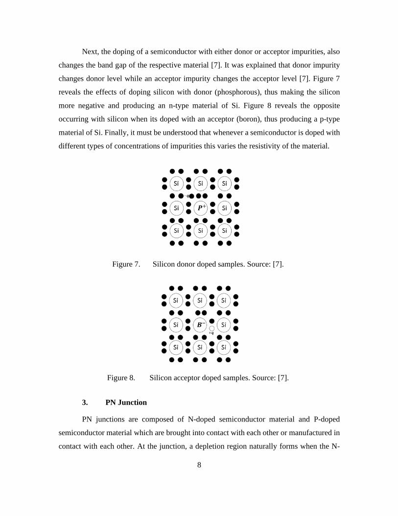
Next, the doping of a semiconductor with either donor or acceptor impurities, also
changes the band gap of the respective material [7]. It was explained that donor impurity
changes donor level while an acceptor impurity changes the acceptor level [7]. Figure 7
reveals the effects of doping silicon with donor (phosphorous), thus making the silicon
more negative and producing an n-type material of Si. Figure 8 reveals the opposite
occurring with silicon when its doped with an acceptor (boron), thus producing a p-type
material of Si. Finally, it must be understood that whenever a semiconductor is doped with
different types of concentrations of impurities this varies the resistivity of the material.
Figure 7. Silicon donor doped samples. Source: [7].
Figure 8. Silicon acceptor doped samples. Source: [7].
3. PN Junction
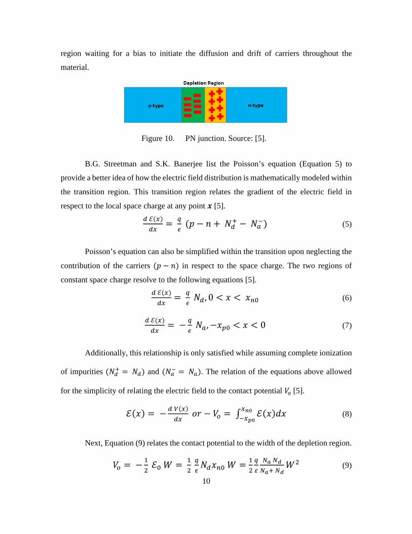
PN junctions are composed of N-doped semiconductor material and P-doped
semiconductor material which are brought into contact with each other or manufactured in
contact with each other. At the junction, a depletion region naturally forms when the N-
9
doped and P-doped material is brought together, or manufactured together. The
semiconductor material can be silicon, gallium, or a III-V compound semiconductor
material such as GaAs. The key to a PN junction using any semiconductor material is that
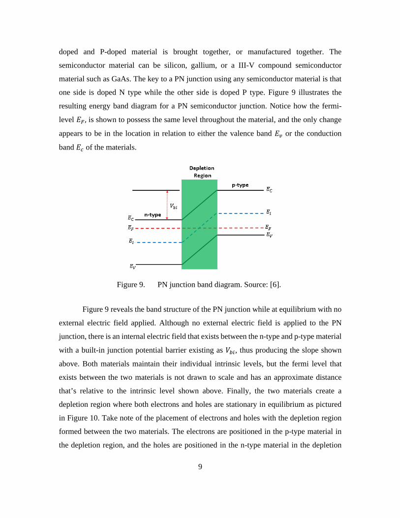
one side is doped N type while the other side is doped P type. Figure 9 illustrates the
resulting energy band diagram for a PN semiconductor junction. Notice how the fermi-
level 𝐸𝐸𝐹𝐹 , is shown to possess the same level throughout the material, and the only change
appears to be in the location in relation to either the valence band 𝐸𝐸𝑣𝑣 or the conduction
band 𝐸𝐸𝑐𝑐 of the materials.
Figure 9. PN junction band diagram. Source: [6].
Figure 9 reveals the band structure of the PN junction while at equilibrium with no
external electric field applied. Although no external electric field is applied to the PN
junction, there is an internal electric field that exists between the n-type and p-type material
with a built-in junction potential barrier existing as 𝑉𝑉𝑏𝑏𝑖𝑖, thus producing the slope shown
above. Both materials maintain their individual intrinsic levels, but the fermi level that
exists between the two materials is not drawn to scale and has an approximate distance
that’s relative to the intrinsic level shown above. Finally, the two materials create a
depletion region where both electrons and holes are stationary in equilibrium as pictured
in Figure 10. Take note of the placement of electrons and holes with the depletion region
formed between the two materials. The electrons are positioned in the p-type material in
the depletion region, and the holes are positioned in the n-type material in the depletion
10
region waiting for a bias to initiate the diffusion and drift of carriers throughout the
material.
Figure 10. PN junction. Source: [5].
B.G. Streetman and S.K. Banerjee list the Poisson’s equation (Equation 5) to
provide a better idea of how the electric field distribution is mathematically modeled within
the transition region. This transition region relates the gradient of the electric field in
respect to the local space charge at any point 𝒙𝒙 [5].
𝑑𝑑 ℰ(𝑥𝑥)𝑑𝑑𝑥𝑥
= 𝑞𝑞𝜖𝜖
(𝑝𝑝 − 𝑛𝑛 + 𝑁𝑁𝑑𝑑+ − 𝑁𝑁𝑎𝑎−) (5)
Poisson’s equation can also be simplified within the transition upon neglecting the
contribution of the carriers (𝑝𝑝 − 𝑛𝑛) in respect to the space charge. The two regions of
constant space charge resolve to the following equations [5].
𝑑𝑑 ℰ(𝑥𝑥)𝑑𝑑𝑥𝑥
= 𝑞𝑞𝜖𝜖
𝑁𝑁𝑑𝑑 , 0 < 𝑥𝑥 < 𝑥𝑥𝑛𝑛0 (6)
𝑑𝑑 ℰ(𝑥𝑥)𝑑𝑑𝑥𝑥
= −𝑞𝑞𝜖𝜖
𝑁𝑁𝑎𝑎,−𝑥𝑥𝑝𝑝0 < 𝑥𝑥 < 0 (7)
Additionally, this relationship is only satisfied while assuming complete ionization
of impurities (𝑁𝑁𝑑𝑑+ = 𝑁𝑁𝑑𝑑) and (𝑁𝑁𝑎𝑎− = 𝑁𝑁𝑎𝑎). The relation of the equations above allowed
for the simplicity of relating the electric field to the contact potential 𝑉𝑉𝑜𝑜 [5].
ℰ(𝑥𝑥) = −𝑑𝑑 𝑉𝑉(𝑥𝑥)𝑑𝑑𝑥𝑥
𝑜𝑜𝑜𝑜 − 𝑉𝑉𝑜𝑜 = ∫ ℰ(𝑥𝑥)𝑑𝑑𝑥𝑥𝑥𝑥𝑛𝑛0−𝑥𝑥𝑝𝑝0
(8)
Next, Equation (9) relates the contact potential to the width of the depletion region.
𝑉𝑉𝑜𝑜 = −12
ℰ0 𝑊𝑊 = 12
𝑞𝑞𝜖𝜖𝑁𝑁𝑑𝑑𝑥𝑥𝑛𝑛0 𝑊𝑊 = 1
2𝑞𝑞𝜀𝜀𝑁𝑁𝑎𝑎 𝑁𝑁𝑑𝑑𝑁𝑁𝑎𝑎+ 𝑁𝑁𝑑𝑑
𝑊𝑊2 (9)

11
Finally, Equation (10) reveals the resulting solution for width of the depletion
region in respect to the n-type and p-type materials, individual doping concentrations, and
shared initial contact potential.
𝑊𝑊 = �2𝜖𝜖𝑉𝑉0𝑞𝑞
𝑁𝑁𝑎𝑎+ 𝑁𝑁𝑑𝑑𝑁𝑁𝑎𝑎 𝑁𝑁𝑑𝑑
(10)
4. Generation Rate and Recombination
B.G. Streetman and S.K. Banerjee explain the process of generation and
recombination of electron-hole pairs within a semiconductor. This effect is achieved by the
material absorbing photons with energy greater than the band gap while balanced by direct
or indirect recombination [5]. Figure 11 illustrates this occurrence more simply. It should
be observed that the energy of the light, or a photon, entering the material is greater than
the bandgap energy that generates electron hole pairs in the existing material. This
phenomenon likewise occurs with similar energies that have the capability of penetrating
the material and having this same effect on the bandgap of the material.
Figure 11. Light generating electron-hole pairs. Source: [6].
Next, the momentum discussed in paragraph 1 will be further discussed with its
effect on the generation and recombination of electron hole pairs in a semiconductor.
In a semiconductor, an intrinsic concentration, 𝑛𝑛𝑖𝑖, of electrons or holes exist, and this
occurs from the thermal generation-recombination between the valence band and
conduction band. Additionally, adding energy to this material creates more of these
particles in its respective material. Energy in the form of increasing temperature, an electric
12
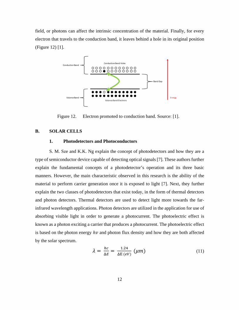
field, or photons can affect the intrinsic concentration of the material. Finally, for every
electron that travels to the conduction band, it leaves behind a hole in its original position
(Figure 12) [1].
Figure 12. Electron promoted to conduction band. Source: [1].
B. SOLAR CELLS
1. Photodetectors and Photoconductors
S. M. Sze and K.K. Ng explain the concept of photodetectors and how they are a
type of semiconductor device capable of detecting optical signals [7]. These authors further
explain the fundamental concepts of a photodetector’s operation and its three basic
manners. However, the main characteristic observed in this research is the ability of the
material to perform carrier generation once it is exposed to light [7]. Next, they further
explain the two classes of photodetectors that exist today, in the form of thermal detectors
and photon detectors. Thermal detectors are used to detect light more towards the far-
infrared wavelength applications. Photon detectors are utilized in the application for use of
absorbing visible light in order to generate a photocurrent. The photoelectric effect is
known as a photon exciting a carrier that produces a photocurrent. The photoelectric effect
is based on the photon energy ℎ𝑣𝑣 and photon flux density and how they are both affected
by the solar spectrum.
𝜆𝜆 = ℎ𝑐𝑐Δ𝐸𝐸
= 1.24ΔΕ (𝑒𝑒𝑉𝑉)
(𝜇𝜇𝜇𝜇) (11)
13
Equation (11) reveals the relationship between the wavelength 𝜆𝜆, the speed of light
𝑐𝑐, and the transition of energy levels ΔΕ [7]. The photon energy must possess the
characteristic ℎ𝑣𝑣 > ΔΕ in order to cause excitation associated with the minimum
wavelength necessary for detection. Photon energy is also utilized to determine the
quantum efficiency.
𝜂𝜂 = 𝐼𝐼𝑝𝑝ℎ𝑞𝑞𝑞𝑞
= 𝐼𝐼𝑝𝑝ℎ𝑞𝑞
( ℎ𝑣𝑣𝑃𝑃𝑜𝑜𝑝𝑝𝑜𝑜
) (12)
Next, the quantum efficiency is defined as the number of carriers produced per
photon. Equation (12) provides the parameters needed to evaluate the quantum efficiency
of a photodetector. Besides observing the photon energy, the photocurrent 𝐼𝐼𝑝𝑝ℎ, photon flux
𝜙𝜙 and the optical power 𝑃𝑃𝑜𝑜𝑝𝑝𝑜𝑜 are considered. S. M. Sze and K.K. Ng further explain with
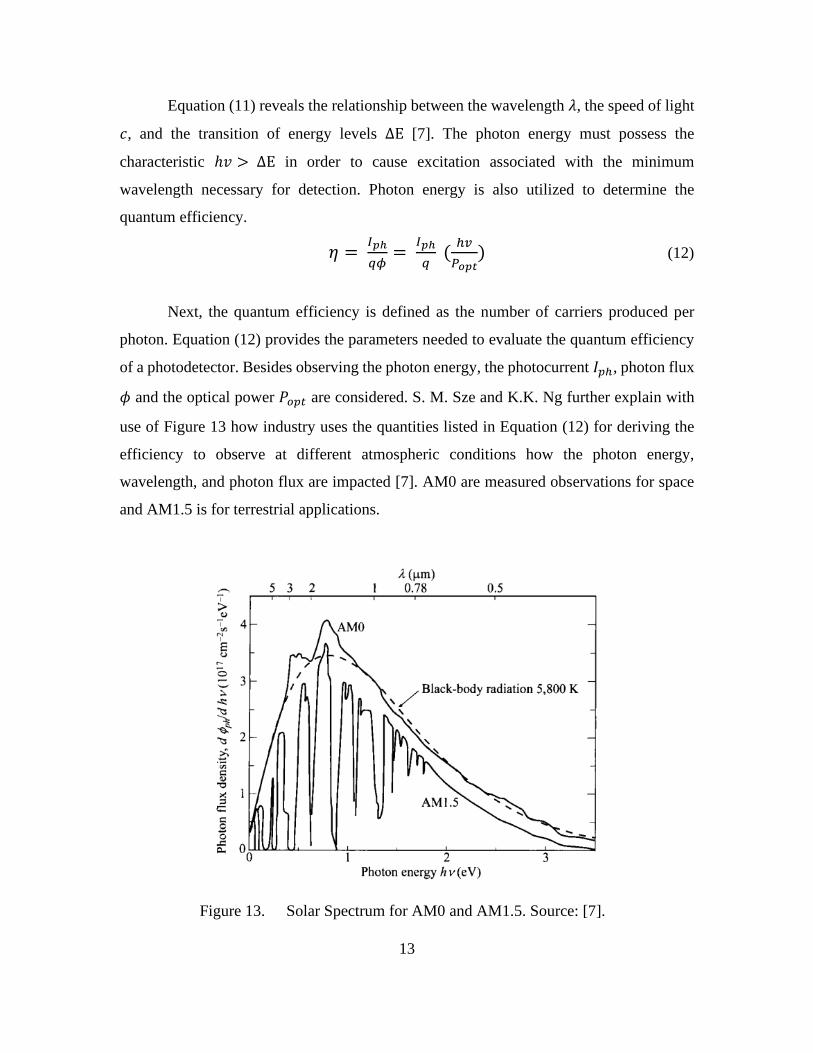
use of Figure 13 how industry uses the quantities listed in Equation (12) for deriving the
efficiency to observe at different atmospheric conditions how the photon energy,
wavelength, and photon flux are impacted [7]. AM0 are measured observations for space
and AM1.5 is for terrestrial applications.
Figure 13. Solar Spectrum for AM0 and AM1.5. Source: [7].
14
2. Solar Cell Operation
S. M. Sze and K.K. Ng discuss considerations while designing solar cells and the
three factors that exist for the optimal design. They declare high efficiency, inexpensive
costs, and exceptional reliability are suited for an optimal design [7]. For example, crystal
silicon solar cells are widely used with the best reported efficiency reaching higher than
22% [7]. Thin-filmed solar cells are desired for some applications due to their low-cost in
processing and materials used. However, their disadvantages are poor efficiency and
continuing instability. Thin-filmed solar cells have either single-junction or multi-junction
cell structures. Multiple-junction cells have proven to possess higher efficiencies than
single-junction cells, due to their different designs and configurations. Currently, three-
junction cells designed with compound semiconductors of GaAs/InGaAs and
InGaP/InGaAs/Ge have produced efficiencies higher than 30%, the highest of any structure
[7]. M. Lundstrom discuss the concept of measuring efficiency of a solar cell, which can
be simply focused on the short circuit current and the open circuit voltage [6]. He also
explains the importance of the calculated fill factor of the solar cell to find the output power
𝑃𝑃𝑜𝑜𝑜𝑜𝑜𝑜 [6]. Equations (13) and (14) are provided for reference.
𝑃𝑃𝑜𝑜𝑜𝑜𝑜𝑜 = 𝐼𝐼𝑆𝑆𝐶𝐶𝑉𝑉𝑂𝑂𝐶𝐶𝐹𝐹𝐹𝐹 (13)
𝜂𝜂 = 𝑃𝑃𝑜𝑜𝑜𝑜𝑜𝑜𝑃𝑃𝑖𝑖𝑛𝑛
= 𝑉𝑉𝑜𝑜𝑜𝑜𝐽𝐽𝑠𝑠𝑜𝑜𝐹𝐹𝐹𝐹𝑃𝑃𝑖𝑖𝑛𝑛
(14)
𝐹𝐹𝐹𝐹 = 𝑃𝑃𝑜𝑜𝑜𝑜𝑜𝑜𝑉𝑉𝑜𝑜𝑜𝑜𝐽𝐽𝑠𝑠𝑜𝑜
(15)
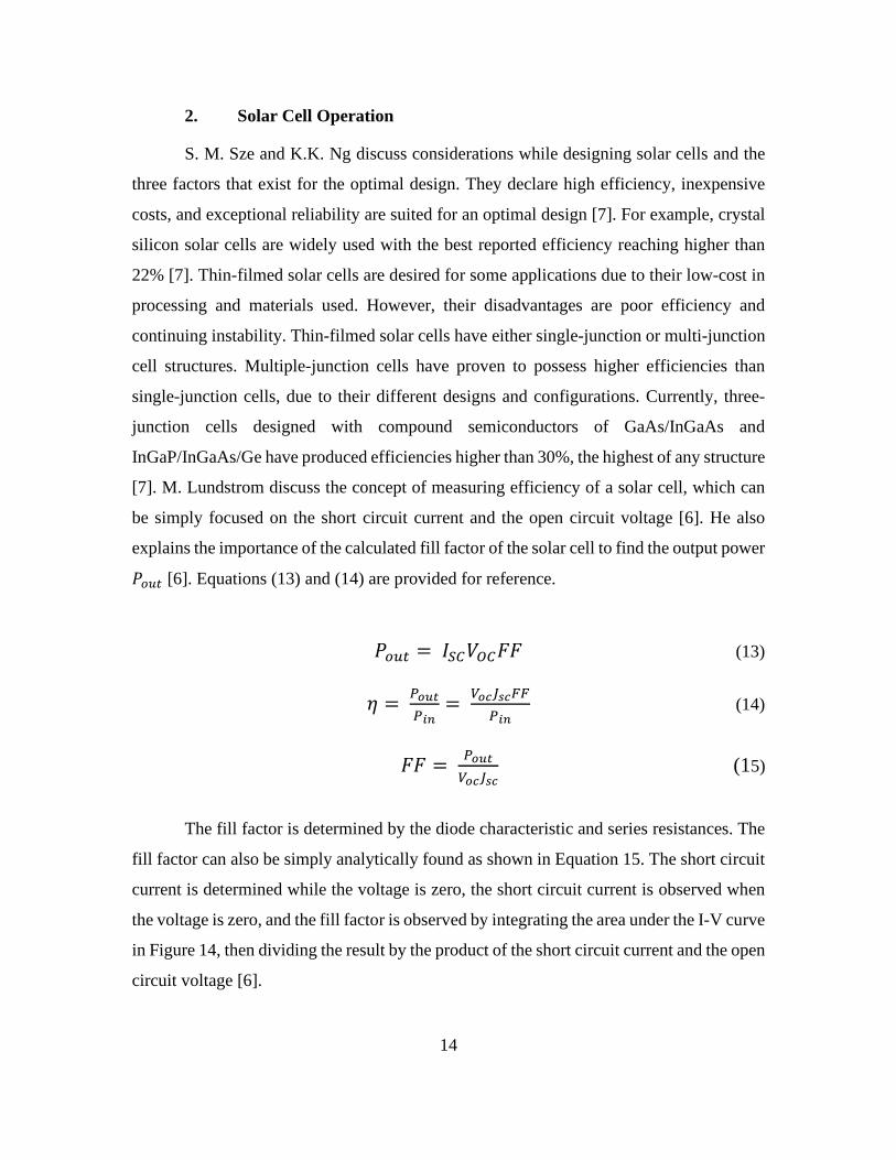
The fill factor is determined by the diode characteristic and series resistances. The
fill factor can also be simply analytically found as shown in Equation 15. The short circuit
current is determined while the voltage is zero, the short circuit current is observed when
the voltage is zero, and the fill factor is observed by integrating the area under the I-V curve
in Figure 14, then dividing the result by the product of the short circuit current and the open
circuit voltage [6].
15
Figure 14. I-V characteristics for solar cell.
C. MULTI-JUNCTION SOLAR CELLS
1. Manufacturing
Multi-junction Solar Cells are known for being able to take advantage of the
theoretical maximum efficiency by combining multiple layers of compound
semiconductors together as discussed previously with GaAs/InGaAs and
InGaP/InGaP/InGaAs/Ge. This was achieved by balancing the expected band gap for both
the respective photocurrent and open-circuit voltage of the semiconductor. Additionally,
efficiency is improved with photon absorption due to how the cells are arranged in their
respective design that takes advantage of the lowest band gap present within the entire
multi-junction design. These multi-junction cells are produced as thin-films [7].
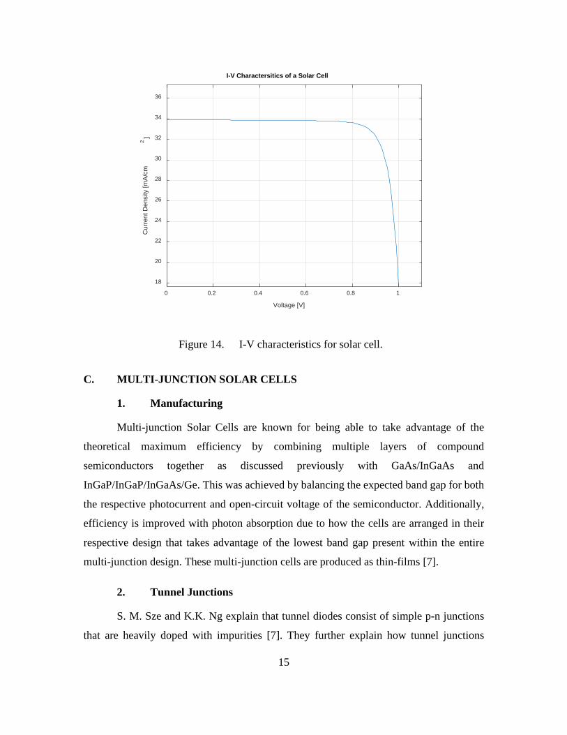
2. Tunnel Junctions
S. M. Sze and K.K. Ng explain that tunnel diodes consist of simple p-n junctions
that are heavily doped with impurities [7]. They further explain how tunnel junctions
0 0.2 0.4 0.6 0.8 1
Voltage [V]
18
20
22
24
26
28
30
32
34
36
Cur
rent
Den
sity
[mA/
cm2
]
I-V Charactersitics of a Solar Cell
16
enable the tunneling process that allows electron tunneling from the valence band to the
conduction band when a reverse bias is applied. Additionally, the tunneling process can
either be direct or indirect.
Figure 15. Static I-V characteristics of a tunnel diode. Source: [7].
Furthermore, they explain the behavior of the static current and voltage behavior of
a tunnel diode in Figure 16. Both the peak and valley voltages and currents are shown for
their static behavior [7].

17
Figure 16. Three components of static characteristics. Source: [7].
Finally, S. M. Sze and K.K. Ng reveal the total static characteristics of the tunnel
diode broken into three current components in Figure 16 [7]. The components are diffusion
current, excess current, and tunneling current. They further explain the static characteristics
at equilibrium. At equilibrium, it was explained that the tunneling current is the current that
moves from the conduction band to an empty state in the valence band. Next, the excess
current is caused by carrier tunneling this effect is caused by energy states that exist within
a forbidden gap that appear in both the valence band and conduction band. Conclusively,
diffusion current for a tunneling diode is what allows the actual current to flow between
both materials present in the p-n junction.

18
THIS PAGE INTENTIONALLY LEFT BLANK
19
III. METHODOLOGY
A. MODELED CELL
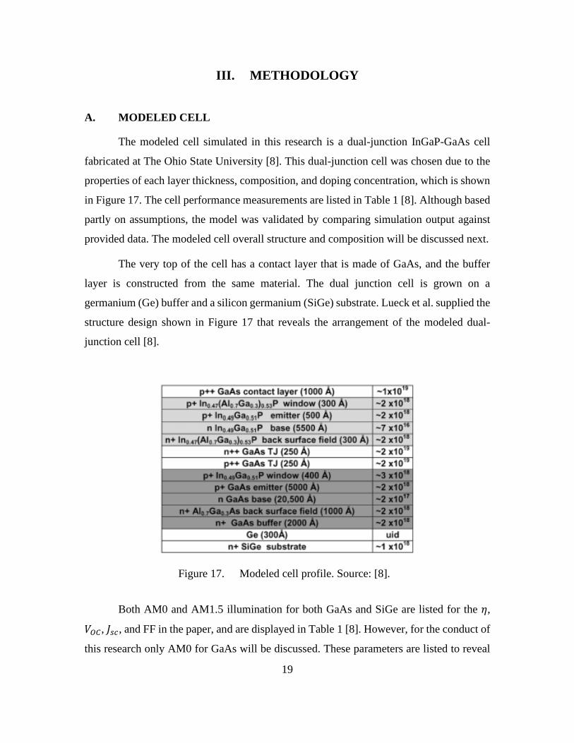
The modeled cell simulated in this research is a dual-junction InGaP-GaAs cell
fabricated at The Ohio State University [8]. This dual-junction cell was chosen due to the
properties of each layer thickness, composition, and doping concentration, which is shown
in Figure 17. The cell performance measurements are listed in Table 1 [8]. Although based
partly on assumptions, the model was validated by comparing simulation output against
provided data. The modeled cell overall structure and composition will be discussed next.
The very top of the cell has a contact layer that is made of GaAs, and the buffer
layer is constructed from the same material. The dual junction cell is grown on a
germanium (Ge) buffer and a silicon germanium (SiGe) substrate. Lueck et al. supplied the
structure design shown in Figure 17 that reveals the arrangement of the modeled dual-
junction cell [8].
Figure 17. Modeled cell profile. Source: [8].
Both AM0 and AM1.5 illumination for both GaAs and SiGe are listed for the 𝜂𝜂,
𝑉𝑉𝑂𝑂𝐶𝐶, 𝐽𝐽𝑠𝑠𝑐𝑐, and FF in the paper, and are displayed in Table 1 [8]. However, for the conduct of
this research only AM0 for GaAs will be discussed. These parameters are listed to reveal

20
the overall performance of this modeled dual-junction cell. The total area efficiency for
AM0 was recorded at 18.6% for the cell grown on a GaAs substrate with a 𝑉𝑉𝑂𝑂𝐶𝐶 of 2.34 V,
𝐽𝐽𝑆𝑆𝐶𝐶 of 13.08 𝜇𝜇𝑚𝑚/𝑐𝑐𝜇𝜇2, and a FF of 82.5%. These measured quantities are also listed in
Table 1, and they assisted in predicting favorable results between the modeled cell and any
further simulated cells that were produced during this research.
Table 1. Lighted current voltage for GaAs. Source: [8].
GaAs
AM0 AM1.5G
𝐽𝐽𝑆𝑆𝐶𝐶 (𝜇𝜇𝑚𝑚/𝑐𝑐𝜇𝜇2) 13.08 10.9 𝑉𝑉𝑂𝑂𝐶𝐶(𝑉𝑉) 2.34 2.32 𝐹𝐹𝐹𝐹(%) 82.5 79.0 𝜂𝜂(%) 18.6 20.0
Lueck et al. provided Figure 18 to illustrate the I-V characteristics of the
performance for the modeled cell at both AM0 and AM1.5. The authors also noted that the
measurements performed in Figure 18 were the results of AM0 and AM1.5 illumination of
GaInP/GaAs dual-junction cells on GaAs and SiGe substrates. AM0 measurements were
performed at the NASA Glenn Research Center, and the AM1.5G were performed at the
National Renewable Energy Laboratory (NREL). The baseline performance for the GaAs
substrate will be measurements recorded for AM0.

21
Figure 18. I-V measurements under AM0 and AM1.5G. Source: [8].
B. SILVACO ATLAS
Silvaco ATLAS is primarily used to model and simulate semiconductors in the
semiconductor industry. Silvaco ATLAS was used heavily during this research to simulate
the dual-junction cell. The baseline of the modeled cell depicted in the last section was first
created to ensure accuracy of measurements before any further designs were introduced.
Silvaco ATLAS enables the user to perform simulations for two-dimensional and three-
dimensional semiconductors. Silvaco ATLAS possesses its own scripting language for the
designed semiconductor device to be tested. If Silvaco ATLAS is executed properly, the
result will be as shown in Figure 19.

22
Figure 19. Modeled cell created in Silvaco
In order to ensure the correct and efficient design of any semiconductor, the order
of statements for the mesh definition, structural definition, and solution groups must be
constructed. For the mesh definition that exist within a simulation the user must carefully
allocate mesh nodes at their defined regions, especially at regions of high activity.
The mesh definition ensures that the simulated design space will perform as designed. This
definition also directly affects the generation and recombination of electron-hole pairs
throughout the entirety of the structure. The structural definitions ensure that every layer
of material is precisely placed according the thickness and doping concentration specified
in the design. The top section, tunneling junction, bottom section, and electrodes are
depicted in Figure 19. Finally, the solution groups were important to ensure the necessary
data was available for analysis later in the research in order to determine the performance
of each designed cell. The solutions utilized heavily throughout this research were
solutions of the designed cell under forward biased conditions in order to extract the 𝜂𝜂,
𝑉𝑉𝑂𝑂𝐶𝐶, 𝐽𝐽𝑠𝑠𝑐𝑐, and FF .
23
C. MOBILITY
The ability of electrons and holes to travel through a material is known as electron
mobility 𝜇𝜇𝑛𝑛 and hole mobility 𝜇𝜇𝑝𝑝, respectively. The mobility of either of these carriers is
utilized as a function of doping for binary materials and this function is even more complex
for both ternary and quaternary materials. This is due to the complexities involved with the
various doping concentrations of these materials. Walsh discussed in depth the modeling
constants and mobility parameters for GaAs, GaP, AlAs, and AlP for calculating the
approximate mobilities for use within Silvaco ATLAS [1]. The modeling constants and
mobility parameters were used extensively to ensure the modeling that was previously
utilized by Walsh remained consistent throughout the performance of this research. The
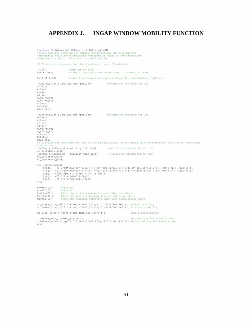
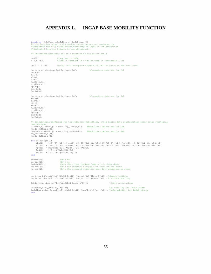
individual MATLAB functions and associated values are listed in the Appendices F
through I, L, and N.
D. NEARLY ORTHOGONAL LATIN HYPERCUBE
The purpose of utilizing NOLH is to ensure designs are produced with minimal
correlations while finding nearly orthogonal designs. The use of NOLH is reinforced by
the user observing the design space not prematurely limited. In addition, an optimal
solution is based on a Latin hypercube design that possesses an orthogonal regression
matrix that includes quadratics and two-way interactions [9].
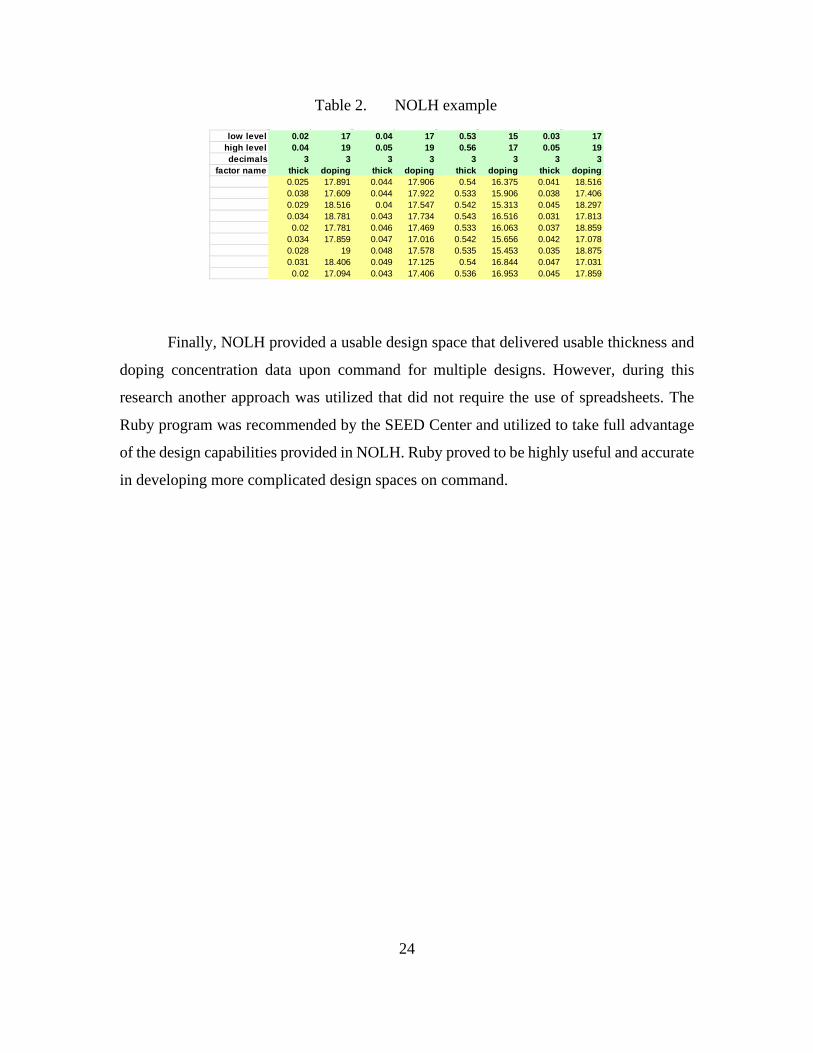
Next, Table 2 reveals the implementation of a solution from NOLH. This
spreadsheet supplied from the NPS Simulation, Experiments and Efficient Design (SEED)
Center for Data Farming was helpful in understanding how NOLH produces results from
user inputs. The user is required to supply the minimum limits, maximum limits, and
desired decimal placement solution of the resulting matrix. It should be observed that the
resulting solution provides nearly uncorrelated solutions for both thickness and doping
concentration. The spreadsheet utilized in Table 2 was hard coded for 22 factors that
provided up to 262 different results for each column of data.
24
Table 2. NOLH example
Finally, NOLH provided a usable design space that delivered usable thickness and
doping concentration data upon command for multiple designs. However, during this
research another approach was utilized that did not require the use of spreadsheets. The
Ruby program was recommended by the SEED Center and utilized to take full advantage
of the design capabilities provided in NOLH. Ruby proved to be highly useful and accurate
in developing more complicated design spaces on command.
low level 0.02 17 0.04 17 0.53 15 0.03 17high level 0.04 19 0.05 19 0.56 17 0.05 19decimals 3 3 3 3 3 3 3 3
factor name thick doping thick doping thick doping thick doping0.025 17.891 0.044 17.906 0.54 16.375 0.041 18.5160.038 17.609 0.044 17.922 0.533 15.906 0.038 17.4060.029 18.516 0.04 17.547 0.542 15.313 0.045 18.2970.034 18.781 0.043 17.734 0.543 16.516 0.031 17.8130.02 17.781 0.046 17.469 0.533 16.063 0.037 18.859
0.034 17.859 0.047 17.016 0.542 15.656 0.042 17.0780.028 19 0.048 17.578 0.535 15.453 0.035 18.8750.031 18.406 0.049 17.125 0.54 16.844 0.047 17.0310.02 17.094 0.043 17.406 0.536 16.953 0.045 17.859
25
IV. RESULTS
A. MODELED CELL
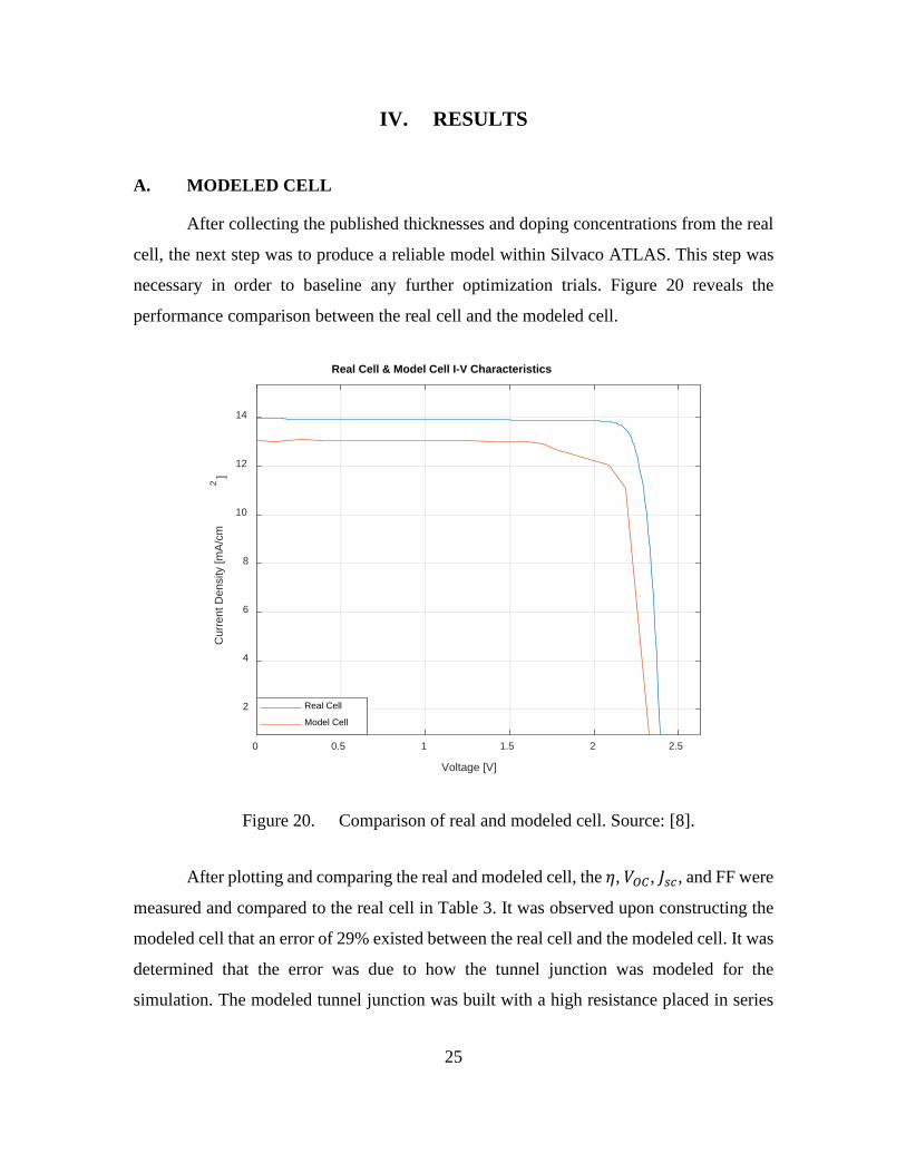
After collecting the published thicknesses and doping concentrations from the real
cell, the next step was to produce a reliable model within Silvaco ATLAS. This step was
necessary in order to baseline any further optimization trials. Figure 20 reveals the
performance comparison between the real cell and the modeled cell.
Figure 20. Comparison of real and modeled cell. Source: [8].
After plotting and comparing the real and modeled cell, the 𝜂𝜂, 𝑉𝑉𝑂𝑂𝐶𝐶, 𝐽𝐽𝑠𝑠𝑐𝑐, and FF were
measured and compared to the real cell in Table 3. It was observed upon constructing the
modeled cell that an error of 29% existed between the real cell and the modeled cell. It was
determined that the error was due to how the tunnel junction was modeled for the
simulation. The modeled tunnel junction was built with a high resistance placed in series
0 0.5 1 1.5 2 2.5
Voltage [V]
2
4
6
8
10
12
14
Cur
rent
Den
sity
[mA/
cm2
]
Real Cell & Model Cell I-V Characteristics
Real Cell
Model Cell
26
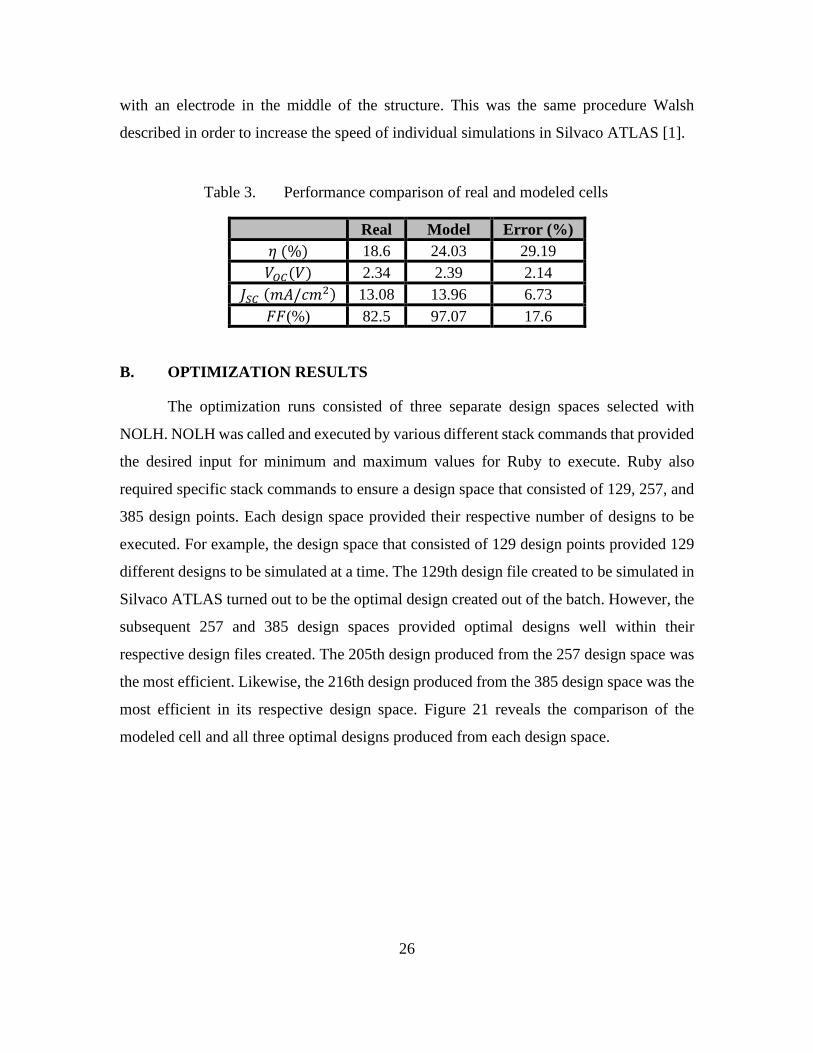
with an electrode in the middle of the structure. This was the same procedure Walsh
described in order to increase the speed of individual simulations in Silvaco ATLAS [1].
Table 3. Performance comparison of real and modeled cells
Real Model Error (%) 𝜂𝜂 (%) 18.6 24.03 29.19 𝑉𝑉𝑂𝑂𝐶𝐶(𝑉𝑉) 2.34 2.39 2.14
𝐽𝐽𝑆𝑆𝐶𝐶 (𝜇𝜇𝑚𝑚/𝑐𝑐𝜇𝜇2) 13.08 13.96 6.73 𝐹𝐹𝐹𝐹(%) 82.5 97.07 17.6
B. OPTIMIZATION RESULTS
The optimization runs consisted of three separate design spaces selected with
NOLH. NOLH was called and executed by various different stack commands that provided
the desired input for minimum and maximum values for Ruby to execute. Ruby also
required specific stack commands to ensure a design space that consisted of 129, 257, and
385 design points. Each design space provided their respective number of designs to be
executed. For example, the design space that consisted of 129 design points provided 129
different designs to be simulated at a time. The 129th design file created to be simulated in
Silvaco ATLAS turned out to be the optimal design created out of the batch. However, the
subsequent 257 and 385 design spaces provided optimal designs well within their
respective design files created. The 205th design produced from the 257 design space was
the most efficient. Likewise, the 216th design produced from the 385 design space was the
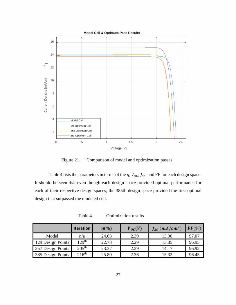
most efficient in its respective design space. Figure 21 reveals the comparison of the
modeled cell and all three optimal designs produced from each design space.
27
Figure 21. Comparison of model and optimization passes
Table 4 lists the parameters in terms of the 𝜂𝜂, 𝑉𝑉𝑂𝑂𝐶𝐶, 𝐽𝐽𝑠𝑠𝑐𝑐, and FF for each design space.
It should be seen that even though each design space provided optimal performance for
each of their respective design spaces, the 385th design space provided the first optimal
design that surpassed the modeled cell.
Table 4. Optimization results
Iteration 𝜼𝜼(%) 𝑽𝑽𝑶𝑶𝑶𝑶(𝑽𝑽) 𝑱𝑱𝑺𝑺𝑶𝑶 (𝒎𝒎𝒎𝒎/𝒄𝒄𝒎𝒎𝟐𝟐) 𝑭𝑭𝑭𝑭(%)
Model n/a 24.03 2.39 13.96 97.07 129 Design Points 129th 22.78 2.29 13.85 96.95 257 Design Points 205th 23.32 2.29 14.17 96.92 385 Design Points 216th 25.80 2.36 15.32 96.45
0 0.5 1 1.5 2 2.5
Voltage [V]
2
4
6
8
10
12
14
16C
urre
nt D
ensi
ty [m
A/cm
2]
Model Cell & Optimum Pass Results
Model Cell
1st Optimum Cell
2nd Optimum Cell
3rd Optimum Cell
28
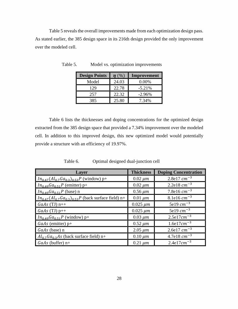
Table 5 reveals the overall improvements made from each optimization design pass.
As stated earlier, the 385 design space in its 216th design provided the only improvement
over the modeled cell.
Table 5. Model vs. optimization improvements
Design Points 𝜼𝜼 (%) Improvement Model 24.03 0.00%
129 22.78 -5.21% 257 22.32 -2.96% 385 25.80 7.34%
Table 6 lists the thicknesses and doping concentrations for the optimized design
extracted from the 385 design space that provided a 7.34% improvement over the modeled
cell. In addition to this improved design, this new optimized model would potentially
provide a structure with an efficiency of 19.97%.
Table 6. Optimal designed dual-junction cell
Layer Thickness Doping Concentration 𝐼𝐼𝑛𝑛0.47(𝑚𝑚𝐴𝐴0.7𝐺𝐺𝐺𝐺0.3)0.53𝑃𝑃 (window) p+ 0.02 𝜇𝜇𝜇𝜇 2.8e17 𝑐𝑐𝜇𝜇−3 𝐼𝐼𝑛𝑛0.49𝐺𝐺𝐺𝐺0.51𝑃𝑃 (emitter) p+ 0.02 𝜇𝜇𝜇𝜇 2.2e18 𝑐𝑐𝜇𝜇−3 𝐼𝐼𝑛𝑛0.49𝐺𝐺𝐺𝐺0.51𝑃𝑃 (base) n 0.56 𝜇𝜇𝜇𝜇 7.8e16 𝑐𝑐𝜇𝜇−3 𝐼𝐼𝑛𝑛0.47(𝑚𝑚𝐴𝐴0.7𝐺𝐺𝐺𝐺0.3)0.53𝑃𝑃 (back surface field) n+ 0.01 𝜇𝜇𝜇𝜇 8.1e16 𝑐𝑐𝜇𝜇−3 𝐺𝐺𝐺𝐺𝑚𝑚𝐺𝐺 (TJ) n++ 0.025 𝜇𝜇𝜇𝜇 5e19 𝑐𝑐𝜇𝜇−3 𝐺𝐺𝐺𝐺𝑚𝑚𝐺𝐺 (TJ) p++ 0.025 𝜇𝜇𝜇𝜇 5e19 𝑐𝑐𝜇𝜇−3 𝐼𝐼𝑛𝑛0.49𝐺𝐺𝐺𝐺0.51𝑃𝑃 (window) p+ 0.03 𝜇𝜇𝜇𝜇 2.5e17𝑐𝑐𝜇𝜇−3 𝐺𝐺𝐺𝐺𝑚𝑚𝐺𝐺 (emitter) p+ 0.52 𝜇𝜇𝜇𝜇 1.6e17𝑐𝑐𝜇𝜇−3 𝐺𝐺𝐺𝐺𝑚𝑚𝐺𝐺 (base) n 2.05 𝜇𝜇𝜇𝜇 2.6e17 𝑐𝑐𝜇𝜇−3 𝑚𝑚𝐴𝐴0.7𝐺𝐺𝐺𝐺0.3𝑚𝑚𝐺𝐺 (back surface field) n+ 0.10 𝜇𝜇𝜇𝜇 4.7e18 𝑐𝑐𝜇𝜇−3 𝐺𝐺𝐺𝐺𝑚𝑚𝐺𝐺 (buffer) n+ 0.21 𝜇𝜇𝜇𝜇 2.4e17𝑐𝑐𝜇𝜇−3
29
V. CONCLUSIONS AND FUTURE WORK
In conclusion, instead of performing an analysis for the largest design space Walsh
could create from the spreadsheet he accessed from the SEED Center for Data Farming. It
was theorized that the optimal design could be found from a smaller design space, resulting
in faster optimization passes that could provide the same if not better results. Additionally,
while pursuing this approach, it was determined that a more efficient process existed to
execute NOLH without the necessity of manipulating the spreadsheet. Dr. Susan Sanchez
from the NPS Operation Research department, was an exceptional resource in
understanding how to utilize Ruby and applying the NOLH instructions in order to create
the desired design space. Upon learning how to operate Ruby proficiently, the next task
was to connect Ruby to MATLAB, and then MATLAB to Silvaco ATLAS. It was also pre-
determined that the modeling of the tunnel junction would have to be simplified by placing
a high resistance in series with an electrode in this region. This implementation still
provided acceptable performance. Finally, for the seamless operation between MATLAB,
Ruby, and Silvaco ATLAS, there were several functions that were built within MATLAB.
These functions were the essential building blocks to ensure efficiency of commands that
were easily executable.
Further research may focus on several areas. First, extending the functionality to
optimize cell design by either material or fractional molar composition. Second,
improvement of the tunnel junction modeling of the doping concentration or thickness.
Third, perform a statistical analysis of the thicknesses and doping concentrations to
optimize a single design space by utilizing the model to analyze and produce a new data
set of values for the thicknesses and doping concentrations. There’s already a MATLAB
function built and listed in Appendix Y to implement. Fourth, a further implementation to
attempt to execute automation of the results as they are analyzed for efficiency. Fifth, the
continuation of the investigation into the optimization of solar cells for the radiation
environment of space.

30
THIS PAGE INTENTIONALLY LEFT BLANK

31
APPENDIX A. RUBY DOWNLOAD AND FAMILIARIZATION
First, Google “Ruby download” in order to find the associated web page below in
Figure 22.
Figure 22. A-1: Find Ruby Download. Source: [10].
Next, I downloaded “ Ruby+Devkit 2.5.5-1 (x64)” compatible for my windows
laptop, as shown in Figure 23.
Figure 23. A-2: Identify Ruby download for your device. Source: [10].
32
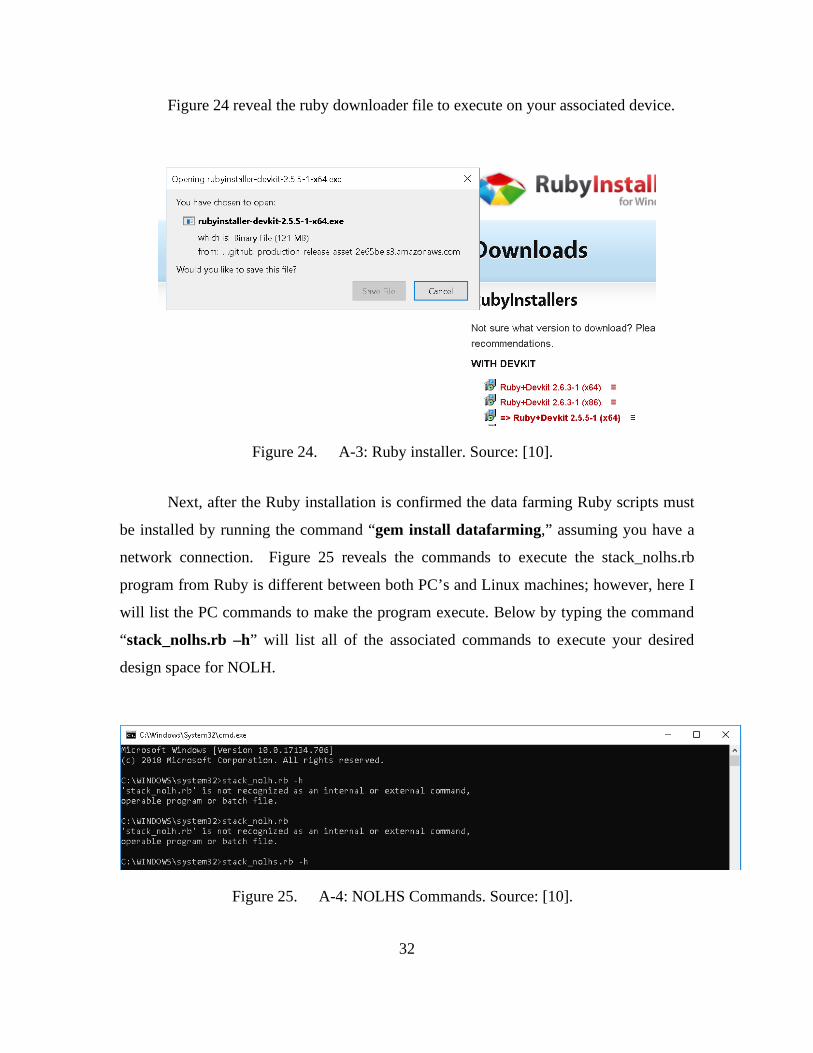
Figure 24 reveal the ruby downloader file to execute on your associated device.
Figure 24. A-3: Ruby installer. Source: [10].
Next, after the Ruby installation is confirmed the data farming Ruby scripts must
be installed by running the command “gem install datafarming,” assuming you have a
network connection. Figure 25 reveals the commands to execute the stack_nolhs.rb
program from Ruby is different between both PC’s and Linux machines; however, here I
will list the PC commands to make the program execute. Below by typing the command
“stack_nolhs.rb –h” will list all of the associated commands to execute your desired
design space for NOLH.
Figure 25. A-4: NOLHS Commands. Source: [10].

33
Figure 26 reveals the results from calling ruby with the “-h” command in the
command window.
Figure 26. A-5: Help Command Results for stack_nolhs.rb. Source: [10].
Next, to familiarize yourself with the results utilized for the research of this
research, the following commands were used.
stack_nolhs.rb -s 1 -e <results.txt >mydesign3.csv

34
The “-s 1” command call the “stack” function to execute “once” for the
stack_nolhs.rb program that will return the desired least amount of design points for our
design that either returned 129-by-9, without tunnel junctions, or 129-by-11, with tunnel
junctions, results for the design.
stack_nolhs.rb -l 129 -e <results.txt >mydesign3.csv
The “-l 129” commands call the “level” function to execute for “129” levels for the
stack_nolhs.rb program that will return the extended amount of design points for our design
that either returned 2817-by-9, without tunnel junctions, or 2817-by-11, with tunnel
junctions, results for the design.
35
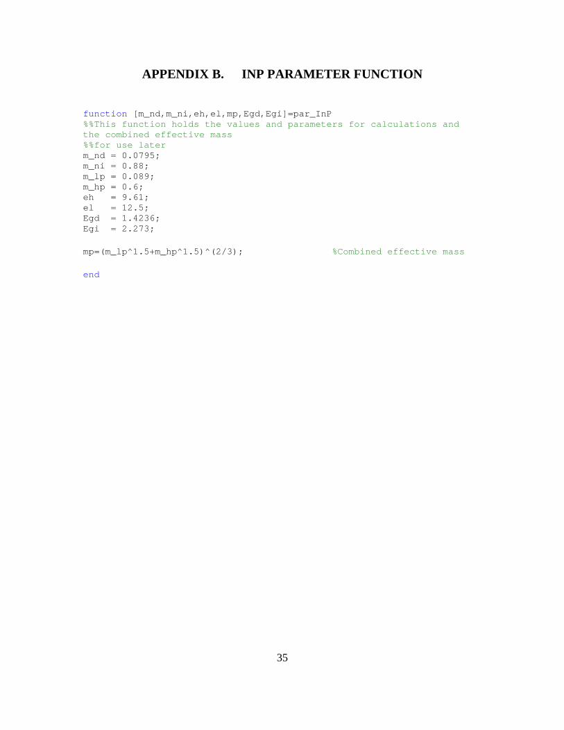
APPENDIX B. INP PARAMETER FUNCTION
function [m_nd,m_ni,eh,el,mp,Egd,Egi]=par_InP %%This function holds the values and parameters for calculations and the combined effective mass %%for use later m_nd = 0.0795; m_ni = 0.88; m_lp = 0.089; m_hp = 0.6; eh = 9.61; el = 12.5; Egd = 1.4236; Egi = 2.273; mp=(m_lp^1.5+m_hp^1.5)^(2/3); %Combined effective mass end

36
THIS PAGE INTENTIONALLY LEFT BLANK
37
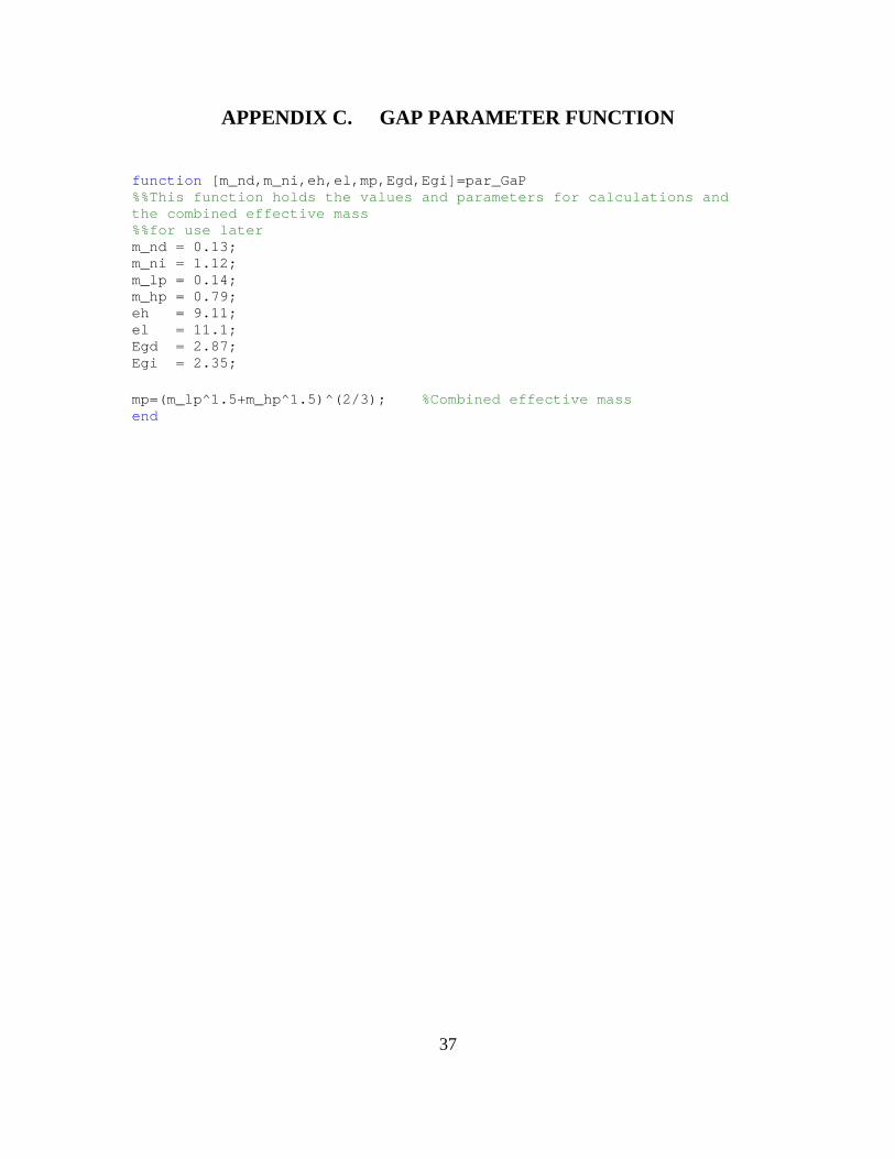
APPENDIX C. GAP PARAMETER FUNCTION
function [m_nd,m_ni,eh,el,mp,Egd,Egi]=par_GaP %%This function holds the values and parameters for calculations and the combined effective mass %%for use later m_nd = 0.13; m_ni = 1.12; m_lp = 0.14; m_hp = 0.79; eh = 9.11; el = 11.1; Egd = 2.87; Egi = 2.35; mp=(m_lp^1.5+m_hp^1.5)^(2/3); %Combined effective mass end

38
THIS PAGE INTENTIONALLY LEFT BLANK

39
APPENDIX D. GAAS PARAMETER FUNCTION
function [m_nd,m_ni,eh,el,mp,Egd,Egi]=par_GaAs %%This function holds the values and parameters for calculations and the combined effective mass %%for use later m_nd = 0.067; m_ni = 0.85; m_lp = 0.082; m_hp = 0.51; eh = 10.89; el = 13.2; Egd = 1.1519; Egi = 1.981; mp=(m_lp^1.5+m_hp^1.5)^(2/3); %Combined effective mass end

40
THIS PAGE INTENTIONALLY LEFT BLANK

41
APPENDIX E. ALAS PARAMETER FUNCTION
function [m_nd,m_ni,eh,el,mp,Egd,Egi]=par_AlAs %%This function holds the values and parameters for calculations and the combined effective mass %%for use later m_nd = 0.15; m_ni = 0.19; m_lp = 0.16; m_hp = 0.81; eh = 8.16; el = 12; Egd = 3.099; Egi = 2.24; mp=(m_lp^1.5+m_hp^1.5)^(2/3); %Combined effective mass end

42
THIS PAGE INTENTIONALLY LEFT BLANK

43
APPENDIX F. ALAS MOBILITY FUNCTION
function [AlAsmu_n,AlAsmu_p,mu_1n,mu_1p,mu_2n,mu_2p] = mobility_AlAs(T,N) %This function is used to calculate the mobility of e-'s and h+'s for AlAs mu_1n=10; mu_1p=10; mu_2n=400; mu_2p=200; alphan=0; alphap=0; betan=-2.1; betap=-2.24; gaman=-3; gamap=-1.464; sigman=1; sigmap=.488; Ncritn=5.46e17; Ncritp=3.48e17; %Electron mobility AlAsmu_n=mu_1n*(T/300)^alphan + (mu_2n*(T/300)^betan - mu_1n*(T/300)^alphan)./(1+(T/300)^gaman.*(N./Ncritn).^sigman); %Hole mobility AlAsmu_p=mu_1p*(T/300)^alphap + (mu_2p*(T/300)^betap - mu_1p*(T/300)^alphap)./(1+(T/300)^gamap.*(N./Ncritp).^sigmap); end

44
THIS PAGE INTENTIONALLY LEFT BLANK

45
APPENDIX G. GAAS MOBILITY FUNCTION
%This function is used to calculate the mobility of e-'s and h+'s for GaAs function [GaAsmu_n,GaAsmu_p] = mobility_GaAs(T,N) mu_1n=500; mu_1p=20; mu_2n=9400; mu_2p=491.5; alphan=0; alphap=0; betan=-2.1; betap=-2.2; gaman=-1.182; gamap=-1.14; sigman=0.394; sigmap=.38; Ncritn=6e16; Ncritp=1.48e17; %Electron mobility GaAsmu_n=mu_1n*(T/300)^alphan + (mu_2n*(T/300)^betan - mu_1n*(T/300)^alphan)./(1+(T/300)^gaman.*(N./Ncritn).^sigman); %Hole mobility GaAsmu_p=mu_1p*(T/300)^alphap + (mu_2p*(T/300)^betap - mu_1p*(T/300)^alphap)./(1+(T/300)^gamap.*(N./Ncritp).^sigmap); end

46
THIS PAGE INTENTIONALLY LEFT BLANK

47
APPENDIX H. GAP MOBILITY FUNCTION
%This function is used to calculate the mobility of e-'s and h+'s for GaPh function [GaPhmu_n,GaPhmu_p,mu_1n,mu_1p,mu_2n,mu_2p] = mobility_GaPh(T,N) mu_1n=10; mu_1p=10; mu_2n=152; mu_2p=147; alphan=0; alphap=0; betan=-1.6; betap=-1.98; gaman=-0.568; gamap=0; sigman=0.8; sigmap=0.85; Ncritn=4.4e18; Ncritp=1e18; %Electron mobility GaPhmu_n=mu_1n*(T/300)^alphan + (mu_2n*(T/300)^betan - mu_1n*(T/300)^alphan)./(1+(T/300)^gaman.*(N./Ncritn).^sigman); %Hole mobility GaPhmu_p=mu_1p*(T/300)^alphap + (mu_2p*(T/300)^betap - mu_1p*(T/300)^alphap)./(1+(T/300)^gamap.*(N./Ncritp).^sigmap); end

48
THIS PAGE INTENTIONALLY LEFT BLANK
49
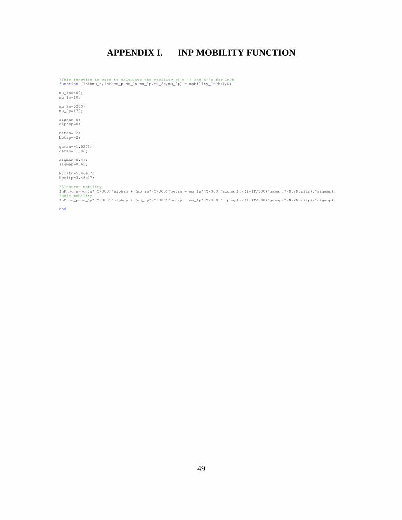
APPENDIX I. INP MOBILITY FUNCTION
%This function is used to calculate the mobility of e-'s and h+'s for InPh function [InPhmu_n,InPhmu_p,mu_1n,mu_1p,mu_2n,mu_2p] = mobility_InPh(T,N) mu_1n=400; mu_1p=10; mu_2n=5200; mu_2p=170; alphan=0; alphap=0; betan=-2; betap=-2; gaman=-1.5275; gamap=-1.86; sigman=0.47; sigmap=0.62; Ncritn=5.46e17; Ncritp=3.48e17; %Electron mobility InPhmu_n=mu_1n*(T/300)^alphan + (mu_2n*(T/300)^betan - mu_1n*(T/300)^alphan)./(1+(T/300)^gaman.*(N./Ncritn).^sigman); %Hole mobility InPhmu_p=mu_1p*(T/300)^alphap + (mu_2p*(T/300)^betap - mu_1p*(T/300)^alphap)./(1+(T/300)^gamap.*(N./Ncritp).^sigmap); end

50
THIS PAGE INTENTIONALLY LEFT BLANK
51
APPENDIX J. INGAP WINDOW MOBILITY FUNCTION
function [InGaPwmu_n,InGaPwmu_p]=InGaP_window(N) %%This function takes in the doping concentrations and performs the %%necessary mobility calculations necessary to input to the associated %%deckbuild file for Silvaco to run efficiently. %% Parameters necessary for this function to run effiiciently T=300; %Temp set to 300K k=8.617e-5; %Plank's constant in eV to be used in conversion later C=[0.51 0.49]; %Molar fractions/percentages utilized for calculations used late [m_nd,m_ni,eh,el,mp,Egd,Egi]=par_InP; %Parameters obtained for InP eh1=eh; el1=el; e1=eh; e3=el; m_nd1=m_nd; m_ni1=m_ni; mp1=mp; Eg1=Egd; Eg11=Egi; [m_nd,m_ni,eh,el,mp,Egd,Egi]=par_GaP; %Parameters obtained for GaP eh2=eh; el2=el; e2=eh; e4=el; m_nd2=m_nd; m_ni2=m_ni; mp2=mp; Eg2=Egd; Eg22=Egi; %% Calculations performed for the following mobilities, while taking into consideration their molar fractional combinations [InPhmu_n,InPhmu_p] = mobility_InPh(T,N); %Mobilities determined for InP mu_1n=InPhmu_n(5); [GaPhmu_n,GaPhmu_p] = mobility_GaPh(T,N); %Mobilities determined for GaP mu_2n=GaPhmu_n(5); mu_2p=GaPhmu_p(5); for i=1:length(C) ehh(i) =(1+2*[C*((e1-1)/(e1+2))+(1-C)*((e2-1)/(e2+2))])/(1-C*((e1-1)/(e1+2))-(1-C)*((e2-1)/(e2+2))); ell(i) =(1+2*[C*((e3-1)/(e3+2))+(1-C)*((e4-1)/(e4+2))])/(1-C*((e3-1)/(e3+2))-(1-C)*((e4-1)/(e4+2))); mpp(i) =(mp2*mp1)/(C(i)*mp2+(1-C(i))*mp1); Egd(i) =(1-C(i))*Eg1+C(i)*Eg2; Egi(i) =(1-C(i))*Eg11+C(i)*Eg22; end eh=ehh(1); %Sets eh el=ell(2); %Sets el Egd=Egd(1); %Sets the direct bandgap from calculations above Egi=Egi(1); %Sets the indirect bandgap from calculations above mp=mpp(1); %Sets the combined effective mass from calculations above mu_d=(mu_2n*m_nd2^1.5*(1/eh2-1/el2))/(m_nd1^1.5*(1/eh-1/el)); %direct mobility mu_i=(mu_1n*m_ni2^1.5*(1/eh1-1/el1))/(m_ni1^1.5*(1/eh-1/el)); %indirect mobility Rd=1/(1+(m_ni/m_nd)^1.5*exp((Egd-Egi)/(k*T))); %Ratio calculations InGaPwmu_n=mu_d*Rd+mu_i*(1-Rd); %e- mobility for InGaP window InGaPwmu_p=(mu_2p*mp2^1.5*(1/eh2-1/el2))/(mp^1.5*(1/eh-1/el)); %hole mobility for InGaP window end

52
THIS PAGE INTENTIONALLY LEFT BLANK

53
APPENDIX K. INGAP EMITTER MOBILITY FUNCTION
function [InGaPemu_n,InGaPemu_p]=InGaP_emitter(N) %%This function takes in the doping concentrations and performs the %%necessary mobility calculations necessary to input to the associated %%deckbuild file for Silvaco to run efficiently. %% Parameters necessary for this function to run effiiciently T=300; %Temp set to 300K k=8.617e-5; %Plank's constant in eV to be used in conversion later C=[0.51 0.49]; %Molar fractions/percentages utilized for calculations used late [m_nd,m_ni,eh,el,mp,Egd,Egi]=par_InP; %Parameters obtained for InP eh1=eh; el1=el; e1=eh; e3=el; m_nd1=m_nd; m_ni1=m_ni; mp1=mp; Eg1=Egd; Eg11=Egi; [m_nd,m_ni,eh,el,mp,Egd,Egi]=par_GaP; %Parameters obtained for GaP eh2=eh; el2=el; e2=eh; e4=el; m_nd2=m_nd; m_ni2=m_ni; mp2=mp; Eg2=Egd; Eg22=Egi; %% Calculations performed for the following mobilities, while taking into consideration their molar fractional combinations [InPhmu_n,InPhmu_p] = mobility_InPh(T,N); %Mobilities determined for InP mu_1n=InPhmu_n(2); [GaPhmu_n,GaPhmu_p] = mobility_GaPh(T,N); %Mobilities determined for GaP mu_2n=GaPhmu_n(2); mu_2p=GaPhmu_p(2); for i=1:length(C) ehh(i) =(1+2*[C*((e1-1)/(e1+2))+(1-C)*((e2-1)/(e2+2))])/(1-C*((e1-1)/(e1+2))-(1-C)*((e2-1)/(e2+2))); ell(i) =(1+2*[C*((e3-1)/(e3+2))+(1-C)*((e4-1)/(e4+2))])/(1-C*((e3-1)/(e3+2))-(1-C)*((e4-1)/(e4+2))); mpp(i) =(mp2*mp1)/(C(i)*mp2+(1-C(i))*mp1); Egd(i) =(1-C(i))*Eg1+C(i)*Eg2; Egi(i) =(1-C(i))*Eg11+C(i)*Eg22; end eh=ehh(1); %Sets eh el=ell(2); %Sets el Egd=Egd(1); %Sets the direct bandgap from calculations above Egi=Egi(1); %Sets the indirect bandgap from calculations above mp=mpp(1); %Sets the combined effective mass from calculations above mu_d=(mu_2n*m_nd2^1.5*(1/eh2-1/el2))/(m_nd1^1.5*(1/eh-1/el)); %direct mobility mu_i=(mu_1n*m_ni2^1.5*(1/eh1-1/el1))/(m_ni1^1.5*(1/eh-1/el)); %indirect mobility Rd=1/(1+(m_ni/m_nd)^1.5*exp((Egd-Egi)/(k*T))); %Ratio calculations InGaPemu_n=mu_d*Rd+mu_i*(1-Rd); %e- mobility for InGaP emitter InGaPemu_p=(mu_2p*mp2^1.5*(1/eh2-1/el2))/(mp^1.5*(1/eh-1/el));%hole mobility for InGaP emitter end

54
THIS PAGE INTENTIONALLY LEFT BLANK
55
APPENDIX L. INGAP BASE MOBILITY FUNCTION
function [InGaPbmu_n,InGaPbmu_p]=InGaP_base(N) %%This function takes in the doping concentrations and performs the %%necessary mobility calculations necessary to input to the associated %%deckbuild file for Silvaco to run efficiently. %% Parameters necessary for this function to run effiiciently T=300; %Temp set to 300K k=8.617e-5; %Plank's constant in eV to be used in conversion later C=[0.51 0.49]; %Molar fractions/percentages utilized for calculations used later [m_nd,m_ni,eh,el,mp,Egd,Egi]=par_InP; %Parameters obtained for InP eh1=eh; el1=el; e1=eh; e3=el; m_nd1=m_nd; m_ni1=m_ni; mp1=mp; Eg1=Egd; Eg11=Egi; [m_nd,m_ni,eh,el,mp,Egd,Egi]=par_GaP; %Parameters obtained for GaP eh2=eh; el2=el; e2=eh; e4=el; m_nd2=m_nd; m_ni2=m_ni; mp2=mp; Eg2=Egd; Eg22=Egi; %% Calculations performed for the following mobilities, while taking into consideration their molar fractional combinations [InPhmu_n,InPhmu_p] = mobility_InPh(T,N); %Mobilities determined for InP mu_1n=InPhmu_n(3); [GaPhmu_n,GaPhmu_p] = mobility_GaPh(T,N); %Mobilities determined for GaP mu_2n=GaPhmu_n(3); mu_2p=GaPhmu_p(3); for i=1:length(C) ehh(i) =(1+2*[C*((e1-1)/(e1+2))+(1-C)*((e2-1)/(e2+2))])/(1-C*((e1-1)/(e1+2))-(1-C)*((e2-1)/(e2+2))); ell(i) =(1+2*[C*((e3-1)/(e3+2))+(1-C)*((e4-1)/(e4+2))])/(1-C*((e3-1)/(e3+2))-(1-C)*((e4-1)/(e4+2))); mpp(i) =(mp2*mp1)/(C(i)*mp2+(1-C(i))*mp1); Egd(i) =(1-C(i))*Eg1+C(i)*Eg2; Egi(i) =(1-C(i))*Eg11+C(i)*Eg22; end eh=ehh(1); %Sets eh el=ell(2); %Sets el Egd=Egd(1); %Sets the direct bandgap from calculations above Egi=Egi(1); %Sets the indirect bandgap from calculations above mp=mpp(1); %Sets the combined effective mass from calculations above mu_d=(mu_2n*m_nd2^1.5*(1/eh2-1/el2))/(m_nd1^1.5*(1/eh-1/el)); %direct mobility mu_i=(mu_1n*m_ni2^1.5*(1/eh1-1/el1))/(m_ni1^1.5*(1/eh-1/el)); %indirect mobility Rd=1/(1+(m_ni/m_nd)^1.5*exp((Egd-Egi)/(k*T))); %Ratio calculations InGaPbmu_n=mu_d*Rd+mu_i*(1-Rd); %e- mobility for InGaP window InGaPbmu_p=(mu_2p*mp2^1.5*(1/eh2-1/el2))/(mp^1.5*(1/eh-1/el)); %hole mobility for InGaP window end

56
THIS PAGE INTENTIONALLY LEFT BLANK
57
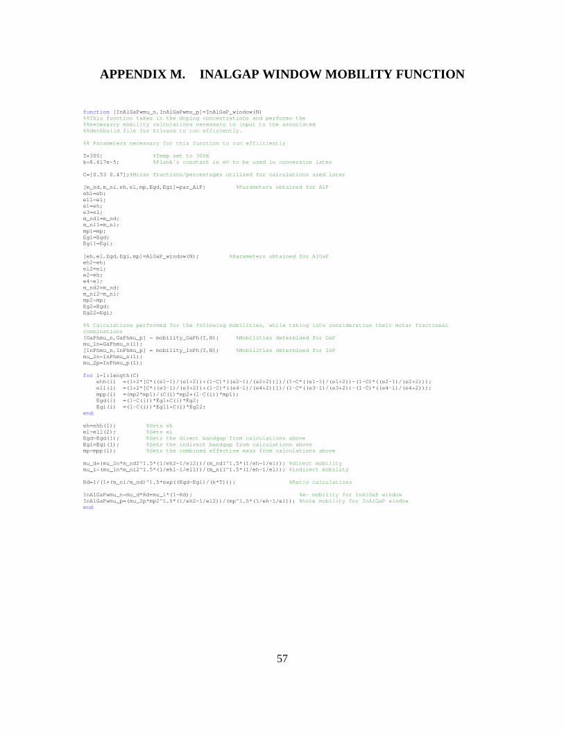
APPENDIX M. INALGAP WINDOW MOBILITY FUNCTION
function [InAlGaPwmu_n,InAlGaPwmu_p]=InAlGaP_window(N) %%This function takes in the doping concentrations and performs the %%necessary mobility calculations necessary to input to the associated %%deckbuild file for Silvaco to run efficiently. %% Parameters necessary for this function to run effiiciently T=300; %Temp set to 300K k=8.617e-5; %Plank's constant in eV to be used in conversion later C=[0.53 0.47];%Molar fractions/percentages utilized for calculations used later [m_nd,m_ni,eh,el,mp,Egd,Egi]=par_AlP; %Parameters obtained for AlP eh1=eh; el1=el; e1=eh; e3=el; m_nd1=m_nd; m_ni1=m_ni; mp1=mp; Eg1=Egd; Eg11=Egi; [eh,el,Egd,Egi,mp]=AlGaP_window(N); %Parameters obtained for AlGaP eh2=eh; el2=el; e2=eh; e4=el; m_nd2=m_nd; m_ni2=m_ni; mp2=mp; Eg2=Egd; Eg22=Egi; %% Calculations performed for the following mobilities, while taking into consideration their molar fractional combinations [GaPhmu_n,GaPhmu_p] = mobility_GaPh(T,N); %Mobilities determined for GaP mu_1n=GaPhmu_n(1); [InPhmu_n,InPhmu_p] = mobility_InPh(T,N); %Mobilities determined for InP mu_2n=InPhmu_n(1); mu_2p=InPhmu_p(1); for i=1:length(C) ehh(i) =(1+2*[C*((e1-1)/(e1+2))+(1-C)*((e2-1)/(e2+2))])/(1-C*((e1-1)/(e1+2))-(1-C)*((e2-1)/(e2+2))); ell(i) =(1+2*[C*((e3-1)/(e3+2))+(1-C)*((e4-1)/(e4+2))])/(1-C*((e3-1)/(e3+2))-(1-C)*((e4-1)/(e4+2))); mpp(i) =(mp2*mp1)/(C(i)*mp2+(1-C(i))*mp1); Egd(i) =(1-C(i))*Eg1+C(i)*Eg2; Egi(i) =(1-C(i))*Eg11+C(i)*Eg22; end eh=ehh(1); %Sets eh el=ell(2); %Sets el Egd=Egd(1); %Sets the direct bandgap from calculations above Egi=Egi(1); %Sets the indirect bandgap from calculations above mp=mpp(1); %Sets the combined effective mass from calculations above mu_d=(mu_2n*m_nd2^1.5*(1/eh2-1/el2))/(m_nd1^1.5*(1/eh-1/el)); %direct mobility mu_i=(mu_1n*m_ni2^1.5*(1/eh1-1/el1))/(m_ni1^1.5*(1/eh-1/el)); %indirect mobility Rd=1/(1+(m_ni/m_nd)^1.5*exp((Egd-Egi)/(k*T))); %Ratio calculations InAlGaPwmu_n=mu_d*Rd+mu_i*(1-Rd); %e- mobility for InAlGaP window InAlGaPwmu_p=(mu_2p*mp2^1.5*(1/eh2-1/el2))/(mp^1.5*(1/eh-1/el)); %hole mobility for InAlGaP window end

58
THIS PAGE INTENTIONALLY LEFT BLANK
59
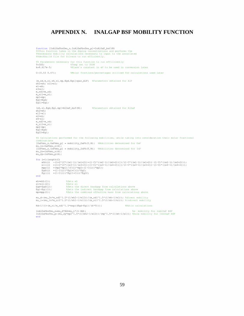
APPENDIX N. INALGAP BSF MOBILITY FUNCTION
function [InAlGaPbsfmu_n,InAlGaPbsfmu_p]=InAlGaP_bsf(N) %%This function takes in the doping concentrations and performs the %%necessary mobility calculations necessary to input to the associated %%deckbuild file for Silvaco to run efficiently. %% Parameters necessary for this function to run effiiciently T=300; %Temp set to 300K k=8.617e-5; %Plank's constant in eV to be used in conversion later C=[0.53 0.47]; %Molar fractions/percentages utilized for calculations used later [m_nd,m_ni,eh,el,mp,Egd,Egi]=par_AlP; %Parameters obtained for AlP eh1=eh; el1=el; e1=eh; e3=el; m_nd1=m_nd; m_ni1=m_ni; mp1=mp; Eg1=Egd; Eg11=Egi; [eh,el,Egd,Egi,mp]=AlGaP_bsf(N); %Parameters obtained for AlGaP eh2=eh; el2=el; e2=eh; e4=el; m_nd2=m_nd; m_ni2=m_ni; mp2=mp; Eg2=Egd; Eg22=Egi; %% Calculations performed for the following mobilities, while taking into consideration their molar fractional combinations [GaPhmu_n,GaPhmu_p] = mobility_GaPh(T,N); %Mobilities determined for GaP mu_1n=GaPhmu_n(4); [InPhmu_n,InPhmu_p] = mobility_InPh(T,N); %Mobilities determined for InP mu_2n=InPhmu_n(4); mu_2p=InPhmu_p(4); for i=1:length(C) ehh(i) =(1+2*[C*((e1-1)/(e1+2))+(1-C)*((e2-1)/(e2+2))])/(1-C*((e1-1)/(e1+2))-(1-C)*((e2-1)/(e2+2))); ell(i) =(1+2*[C*((e3-1)/(e3+2))+(1-C)*((e4-1)/(e4+2))])/(1-C*((e3-1)/(e3+2))-(1-C)*((e4-1)/(e4+2))); mpp(i) =(mp2*mp1)/(C(i)*mp2+(1-C(i))*mp1); Egd(i) =(1-C(i))*Eg1+C(i)*Eg2; Egi(i) =(1-C(i))*Eg11+C(i)*Eg22; end eh=ehh(1); %Sets eh el=ell(2); %Sets el Egd=Egd(1); %Sets the direct bandgap from calculations above Egi=Egi(1); %Sets the indirect bandgap from calculations above mp=mpp(1); %Sets the combined effective mass from calculations above mu_d=(mu_2n*m_nd2^1.5*(1/eh2-1/el2))/(m_nd1^1.5*(1/eh-1/el)); %direct mobility mu_i=(mu_1n*m_ni2^1.5*(1/eh1-1/el1))/(m_ni1^1.5*(1/eh-1/el)); %indirect mobility Rd=1/(1+(m_ni/m_nd)^1.5*exp((Egd-Egi)/(k*T))); %Ratio calculations InAlGaPbsfmu_n=mu_d*Rd+mu_i*(1-Rd); %e- mobility for InAlGaP BSF InAlGaPbsfmu_p=(mu_2p*mp2^1.5*(1/eh2-1/el2))/(mp^1.5*(1/eh-1/el)); %hole mobility for InAlGaP BSF end

60
THIS PAGE INTENTIONALLY LEFT BLANK
61
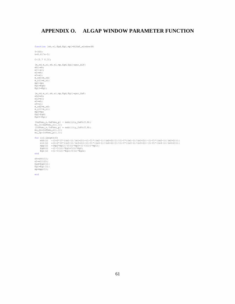
APPENDIX O. ALGAP WINDOW PARAMETER FUNCTION
function [eh,el,Egd,Egi,mp]=AlGaP_window(N) T=300; k=8.617e-5; C=[0.7 0.3]; [m_nd,m_ni,eh,el,mp,Egd,Egi]=par_AlP; eh1=eh; el1=el; e1=eh; e3=el; m_nd1=m_nd; m_ni1=m_ni; mp1=mp; Eg1=Egd; Eg11=Egi; [m_nd,m_ni,eh,el,mp,Egd,Egi]=par_GaP; eh2=eh; el2=el; e2=eh; e4=el; m_nd2=m_nd; m_ni2=m_ni; mp2=mp; Eg2=Egd; Eg22=Egi; [GaPhmu_n,GaPhmu_p] = mobility_GaPh(T,N); mu_1n=GaPhmu_n(:,1); [InPhmu_n,InPhmu_p] = mobility_InPh(T,N); mu_2n=InPhmu_n(:,1); mu_2p=InPhmu_p(:,1); for i=1:length(C) ehh(i) =(1+2*[C*((e1-1)/(e1+2))+(1-C)*((e2-1)/(e2+2))])/(1-C*((e1-1)/(e1+2))-(1-C)*((e2-1)/(e2+2))); ell(i) =(1+2*[C*((e3-1)/(e3+2))+(1-C)*((e4-1)/(e4+2))])/(1-C*((e3-1)/(e3+2))-(1-C)*((e4-1)/(e4+2))); mpp(i) =(mp2*mp1)/(C(i)*mp2+(1-C(i))*mp1); Egd(i) =(1-C(i))*Eg1+C(i)*Eg2; Egi(i) =(1-C(i))*Eg11+C(i)*Eg22; end eh=ehh(1); el=ell(2); Egd=Egd(1); Egi=Egi(1); mp=mpp(1); end

62
THIS PAGE INTENTIONALLY LEFT BLANK

63
APPENDIX P. ALGAAS MOBILITY FUNCTION
function [AlGaAsbsfmu_n,AlGaAsbsfmu_p]=AlGaAs_bsf(N) % clear all; clc; % [N,design_thickness]=input_decks(1,0,1,1,1); T=300; k=8.617e-5; C=[0.7 0.3]; [m_nd,m_ni,eh,el,mp,Egd,Egi]=par_AlAs; eh1=eh; el1=el; e1=eh; e3=el; m_nd1=m_nd; m_ni1=m_ni; mp1=mp; Eg1=Egd; Eg11=Egi; [m_nd,m_ni,eh,el,mp,Egd,Egi]=par_GaAs; eh2=eh; el2=el; e2=eh; e4=el; m_nd2=m_nd; m_ni2=m_ni; mp2=mp; Eg2=Egd; Eg22=Egi; [AlAsmu_n,AlAsmu_p] = mobility_AlAs(T,N); mu_1n=AlAsmu_n(8); [GaAsmu_n,GaAsmu_p] = mobility_GaAs(T,N); mu_2n=GaAsmu_n(8); mu_2p=GaAsmu_p(8); for i=1:length(C) ehh(i) =(1+2*[C*((e1-1)/(e1+2))+(1-C)*((e2-1)/(e2+2))])/(1-C*((e1-1)/(e1+2))-(1-C)*((e2-1)/(e2+2))); ell(i) =(1+2*[C*((e3-1)/(e3+2))+(1-C)*((e4-1)/(e4+2))])/(1-C*((e3-1)/(e3+2))-(1-C)*((e4-1)/(e4+2))); mpp(i) =(mp2*mp1)/(C(i)*mp2+(1-C(i))*mp1); Egd(i) =(1-C(i))*Eg1+C(i)*Eg2; Egi(i) =(1-C(i))*Eg11+C(i)*Eg22; end eh=ehh(1); el=ell(2); Egd=Egd(1); Egi=Egi(1); mp=mpp(1); mu_d=(mu_2n*m_nd2^1.5*(1/eh2-1/el2))/(m_nd1^1.5*(1/eh-1/el)); mu_i=(mu_1n*m_ni2^1.5*(1/eh1-1/el1))/(m_ni1^1.5*(1/eh-1/el)); Rd=1/(1+(m_ni/m_nd)^1.5*exp((Egd-Egi)/(k*T))); AlGaAsbsfmu_n=mu_d*Rd+mu_i*(1-Rd); AlGaAsbsfmu_p=(mu_2p*mp2^1.5*(1/eh2-1/el2))/(mp^1.5*(1/eh-1/el)); end

64
THIS PAGE INTENTIONALLY LEFT BLANK
65
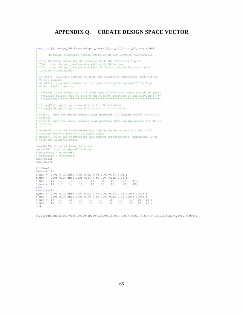
APPENDIX Q. CREATE DESIGN SPACE VECTOR
function [N,design_thickness]=input_decks(TJ,on_off,linux_PC,ruby,model) % % [N,design_thickness]=input_decks(TJ,on_off,linux_PC,ruby,model) % % This function calls get_designspace with the following inputs % TJ=0, runs the get_designspace with only 18 factors % TJ=1, runs the get_designspace with 22 factors including the tunnel % junction thicknesses % % on_off=1, provides command to plot the resulting mobilities from either % TJ=0/1 results % on_off=0, provides command not to plot the resulting mobilities from % either TJ=0/1 results % % **Note: Linux execution will only work if the user opens Matlab in the** % **Public folder, due to that's the current location of the Ruby25x-64*** % **library.************************************************************** % % linux_PC=1, performs command line for PC execution % linux_PC=0, performs command line for linux execution % % ruby=1, runs the stack command that provides 129 design points for 18-22 % factors % ruby=0, runs the level command that provides 2817 design points for 18-22 % factors % % model=0, runs the thicknesses and doping concentratons for for 18-22 % factors derived from the original model % model=1, runs the thicknesses and doping concentratons (including TJ's) % from the original model base=0.55; %orginal base thickness perc=.50; %percentage difference % bmin=base - base*perc; % bmax=base + base*perc; bmin=0.53; bmax=0.57; if TJ==0 factors=18; t_min = [0.01 0.02 bmin 0.01 0.02 0.48 2.03 0.08 0.18]; t_max = [0.05 0.06 bmax 0.05 0.06 0.52 2.07 0.12 0.22]; N_min = [17 17 15 17 17 17 16 17 17]; N_max = [19 19 17 19 19 19 18 19 19]; else factors=22; t_min = [0.01 0.02 bmin 0.01 0.02 0.48 2.03 0.08 0.18 0.005 0.005]; t_max = [0.05 0.06 bmax 0.05 0.06 0.52 2.07 0.12 0.22 0.045 0.045]; N_min = [17 17 15 17 17 17 16 17 17 18 18]; N_max = [19 19 17 19 19 19 18 19 19 20 20]; end [N,design_thickness]=get_designspace(factors,t_min,t_max,N_min,N_max,on_off,linux_PC,ruby,model);

66
THIS PAGE INTENTIONALLY LEFT BLANK
67
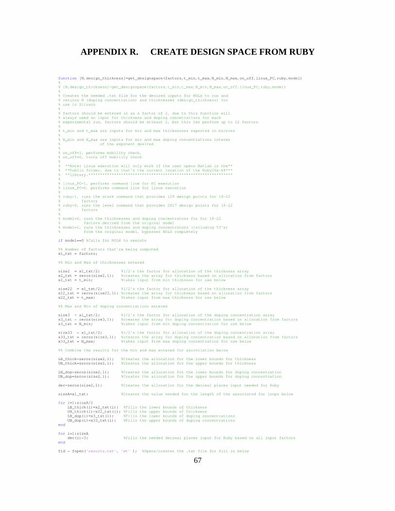
APPENDIX R. CREATE DESIGN SPACE FROM RUBY
function [N,design_thickness]=get_designspace(factors,t_min,t_max,N_min,N_max,on_off,linux_PC,ruby,model) % % [N,design_thickness]=get_designspace(factors,t_min,t_max,N_min,N_max,on_off,linux_PC,ruby,model) % % Creates the needed .txt file for the desired inputs for NOLH to run and % returns N (doping concentration) and thicknesses (design_thickness) for % use in Silvaco % % factors should be entered in as a factor of 2, due to this function will % always need an input for thickness and doping concetrations for each % experimental run, factors should be atleast 2, but this can perform up to 22 factors % % t_min and t_max are inputs for min and max thicknesses expected in microns % % N_min and N_max are inputs for min and max doping concentrations interms % of the exponent desired % % on_off=1, performs mobility check, % on_off=0, turns off mobility check % % **Note: Linux execution will only work if the user opens Matlab in the** % **Public folder, due to that's the current location of the Ruby25x-64*** % **library.************************************************************** % % linux_PC=1, performs command line for PC execution % linux_PC=0, performs command line for linux execution % % ruby=1, runs the stack command that provides 129 design points for 18-22 % factors % ruby=0, runs the level command that provides 2817 design points for 18-22 % factors % % model=0, runs the thicknesses and doping concentratons for for 18-22 % factors derived from the original model % model=1, runs the thicknesses and doping concentratons (including TJ's) % from the original model, bypasses NOLH completely if model==0 %Calls for NOLH to execute %% Number of factors that're being computed x1_txt = factors; %% Min and Max of thicknesses entered size2 = x1_txt/2; %1/2's the factor for allocation of the thickness array x2_txt = zeros(size2,1); %creates the array for thickness based on allocation from factors x2_txt = t_min; %takes input from min thickness for use below size22 = x1_txt/2; %1/2's the factor for allocation of the thickness array x22_txt = zeros(size22,1); %creates the array for thickness based on allocation from factors x22_txt = t_max; %takes input from max thickness for use below %% Max and Min of doping concentrations entered size3 = x1_txt/2; %1/2's the factor for allocation of the doping concentration array x3_txt = zeros(size3,1); %creates the array for doping concentration based on allocation from factors x3_txt = N_min; %takes input from min doping concentration for use below size33 = x1_txt/2; %1/2's the factor for allocation of the doping concentration array x33_txt = zeros(size3,1); %creates the array for doping concentration based on allocation from factors x33_txt = N_max; %takes input from max doping concentration for use below %% Combine the results for the min and max entered for assimilation below LB_thick=zeros(size2,1); %Creates the allocation for the lower bounds for thickness UB_thick=zeros(size2,1); %Creates the allocation for the upper bounds for thickness LB_dop=zeros(size2,1); %Creates the allocation for the lower bounds for doping concentration UB_dop=zeros(size2,1); %Creates the allocation for the upper bounds for doping concentration dec=zeros(size2,1); %Creates the allocation for the decimal places input needed for Ruby sizeA=x1_txt; %Creates the value needed for the length of the associated for loops below for i=1:sizeA/2 LB_thick(i)=x2_txt(i); %Fills the lower bounds of thickness UB_thick(i)=x22_txt(i); %Fills the upper bounds of thickness LB_dop(i)=x3_txt(i); %Fills the lower bounds of doping concentrations UB_dop(i)=x33_txt(i); %Fills the upper bounds of doping concentrations end for i=1:sizeA dec(i)=3; %Fills the needed decimal places input for Ruby based on all input factors end fid = fopen('results.txt', 'wt' ); %Opens/creates the .txt file for fill in below
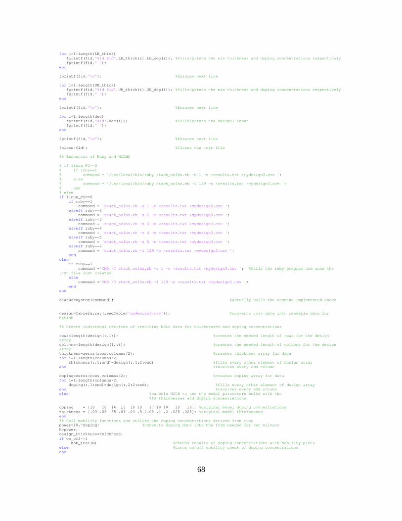
68
for i=1:length(LB_thick) fprintf(fid,"%1d %1d",LB_thick(i),LB_dop(i)); %Fills/prints the min thickness and doping concentrations respectively fprintf(fid," "); end fprintf(fid,"\n"); %Ensures next line for i=1:length(UB_thick) fprintf(fid,"%1d %1d",UB_thick(i),UB_dop(i)); %Fills/prints the max thickness and doping concentrations respectively fprintf(fid," "); end fprintf(fid,"\n"); %Ensures next line for i=1:length(dec) fprintf(fid,"%1d",dec(i)); %Fills/prints the decimal input fprintf(fid," "); end fprintf(fid,"\n"); %Ensures next line fclose(fid); %Closes the .txt file %% Execution of Ruby and NOLHS % if linux_PC==0 % if ruby==1 % command = '/usr/local/bin/ruby stack_nolhs.rb -s 1 -e <results.txt >mydesign3.csv '; % else % command = '/usr/local/bin/ruby stack_nolhs.rb -l 129 -e <results.txt >mydesign3.csv '; % end % else if linux_PC==0 if ruby==1 command = 'stack_nolhs.rb -s 1 -e <results.txt >mydesign3.csv '; elseif ruby==2 command = 'stack_nolhs.rb -s 2 -e <results.txt >mydesign3.csv '; elseif ruby==3 command = 'stack_nolhs.rb -s 3 -e <results.txt >mydesign3.csv '; elseif ruby==4 command = 'stack_nolhs.rb -s 4 -e <results.txt >mydesign3.csv '; elseif ruby==5 command = 'stack_nolhs.rb -s 5 -e <results.txt >mydesign3.csv '; elseif ruby==6 command = 'stack_nolhs.rb -l 129 -e <results.txt >mydesign3.csv '; end else if ruby==1 command ='CMD /C stack_nolhs.rb -s 1 -e <results.txt >mydesign3.csv '; %Calls the ruby program and uses the .txt file just created else command ='CMD /C stack_nolhs.rb -l 129 -e <results.txt >mydesign3.csv '; end end status=system(command); %actually calls the command implemented above design=Table2array(readTable('mydesign3.csv')); %converts .csv data into readable data for Matlab %% Create individual matrices of resulting NOLH data for thicknesses and doping concentrations rows=length(design(:,1)); %creates the needed length of rows for the design array columns=length(design(1,:)); %creates the needed length of columns for the design array thickness=zeros(rows,columns/2); %creates thickness array for data for i=1:length(columns/2) thickness(:,1:end)=design(:,1:2:end); %fills every other element of design array end %receives every odd column doping=zeros(rows,columns/2); %creates doping array for data for i=1:length(columns/2) doping(:,1:end)=design(:,2:2:end); %fills every other element of design array end %receives every odd column else %cancels NOLH to use the model parameters below with the %TJ thicknesses and doping concentrations doping = [18 18 16 18 18 18 17 18 18 19 19]; %original model doping concentrations thickness = [.03 .05 .55 .03 .04 .5 2.05 .1 .2 .025 .025]; %original model thicknesses end %% Call mobility functions and utilize the doping concebtrations derived from ruby power=10.^doping; %converts doping data into the form needed for our Silvaco N=power; design_thickness=thickness; if on_off==1 mob_test(N) %checks results of doping concentrations with mobility plots else %turns on/off mobility check of doping concentrations end

69
APPENDIX S. CREATE DATA VECTORS FROM .LOG FILE
function [eff,Voc, Jsc, FF]=get_designEff(N) % This function retrieves the efficiencies,open circuit voltage, and short % circuit current of the all designs created and places them into an % usuable array % [N,design_thickness]=input_decks(1,0,0,1,0); eff=[]; %creates array for efficency Voc=[]; %creates array for open circuit voltage Jsc=[]; %creates array for short circuit current FF =[]; %creates array for Fill Factor for j=1:length(N(:,1)) command=sprintf('forward_IVSimpleTJ%d.log',j); %generates usable command for a .log file command to be scripted % command=command; if isfile(command) %checks to see whether or not .log file exists [emitterV,emitterVV,baseC,baseCC]=emitter_baseRead(command); %performs execution to pull and read data for current and voltage values from the .log file % disp(j) % disp(solarCell_eff(emitterV,emitterVV,baseC,baseCC)); [effout, Vocout, Jscout, FFout] = solarCell_eff(emitterV,emitterVV,baseC,baseCC); %performs desired calculations for the efficiency for each design [eff]=[eff effout]; %creates array for efficiency [Voc]=[Voc Vocout]; %creates array for open circuit voltage [Jsc]=[Jsc Jscout]; %creates array for short circuit current [FF] =[FF FFout]; %creates array for Fill Factor else eff=[eff 0]; %ensures efficiency array is filled even though .log file may have errorneous data Voc=[Voc 0]; %ensures open circuit voltage array is filled even though .log file may have errorneous data Jsc=[Jsc 0]; %ensures short circuit current array is filled even though .log file may have errorneous data FF =[FF 0]; %ensures Fill Factor array is filled even though .log file may have errorneous data end end end

70
THIS PAGE INTENTIONALLY LEFT BLANK

71
APPENDIX T. READ DATA FROM .LOG FILE
function [emitterV,emitterVV,baseC,baseCC]=emitter_baseRead(command) %% This function reads .log files produced from Silvaco ATLAS s = dir(command); if(s.bytes>0) testlogfile = fopen(command); %loads .log file from Silvac emitterV = []; %creates array for Emitter Voltage for plotting baseC = []; %creates array for Base Current for plotting emitterVV = []; %creates array for Emitter Voltage for calculations baseCC = []; %creates array for Base Current for calculations tline = fgetl(testlogfile); %reads line from file and discards newline character while ischar(tline) %checks if input is a character array datavals = strsplit(tline); %splts string at the delimiter if(datavals{1}=='d') %checks for character 'd' to start reading from .log file if (str2num(datavals{21})>0) emitterV = [emitterV str2num(datavals{13})]; %{14} fills array for Emitter Voltage values baseC = [baseC str2num(datavals{21})]; %{18} fills array for Base Current values end emitterVV = [emitterVV str2num(datavals{13})]; %{14} fills array for Emitter Voltage values baseCC = [baseCC str2num(datavals{21})]; %{18}fills array for Base Current values end tline = fgetl(testlogfile); %ensures lines from .log file are read and discards newline character end fclose(testlogfile); %closes .log file from Silvaco else emitterV = [0]; baseC = [1]; emitterVV = [0]; baseCC = [1]; end

72
THIS PAGE INTENTIONALLY LEFT BLANK

73
APPENDIX U. CREATE 𝜼𝜼,𝑽𝑽𝑶𝑶𝑶𝑶, 𝑱𝑱𝑺𝑺𝑶𝑶, & 𝑭𝑭𝑭𝑭 FROM .LOG FILE
function [eff,Voc,Jsc,FF]=solarCell_eff(emitterV,emitterVV,baseC,baseCC) %% Calculating further parameters necessary for calculations for the performance of our solar cell %Constants needed q=1.61e-19; %charge of one electron kT_q=0.0259; %Einsten relationship Pin=135; %Input power efficiency at AM0 in mW/cm^2 % Pin=100; %Input power efficiency at AM1.5 in mW/cm^2 factor=1e11; %Calculations for the short circuit current Jsc=baseC(1)*factor; %Calculates the short circuit current density in mA/cm^2 %Finding the point where the current is approximately zero loc_neg = find(baseCC<0,1); %locates first negative value loc_pos = find(baseCC>0,length(baseCC)); %locates positive values if(~isempty(loc_neg)) %checks whether loc_neg is emtpy last_pos=loc_pos(end); %locates last positive value y1=baseCC(loc_neg)*factor; %provides the negative value of the current y2=baseCC(last_pos)*factor; %provides the last positive value of the current dy=y2-y1; %change in y x1=emitterVV(loc_neg); %provides the value of voltage respective to current x2=emitterVV(last_pos); %provides the value of voltage respective to current dx=x2-x1; %change in x m=dy/dx; %calculates slope, m b=y1-m*x1; %calculates constant for slope intercept equation Voc=-y1/m+x1; %calculates Voc for the design FF=trapz(emitterV,baseC.*factor)/(Jsc*Voc); %Calculates the Fill Factor of the Solar Cell Pout=Jsc*Voc*FF; %Calculates the output power of the solar cell eff=Pout/Pin; %Calculates the efficiency of the solar cell else %if loc_neg is empty a zero is applied to the following Voc=0; FF=0; Pout=0; eff=0; end end

74
THIS PAGE INTENTIONALLY LEFT BLANK
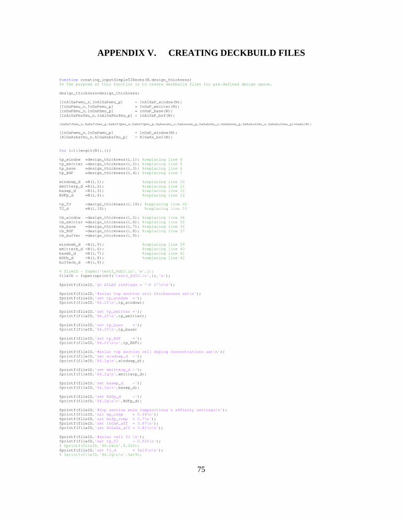
75
APPENDIX V. CREATING DECKBUILD FILES
function creating_inputSimpleTJDecks(N,design_thickness) %% The purpose of this function is to create deckbuild files for pre-defined design space. design_thickness=design_thickness; [InAlGaPwmu_n,InAlGaPwmu_p] = InAlGaP_window(N); [InGaPemu_n,InGaPemu_p] = InGaP_emitter(N); [InGaPbmu_n,InGaPbmu_p] = InGaP_base(N); [InAlGaPbsfmu_n,InAlGaPbsfmu_p] = InAlGaP_bsf(N); [GaAsTJnmu_n,GaAsTJnmu_p,GaAsTJpmu_n,GaAsTJpmu_p,GaAsenmu_n,GaAsenmu_p,GaAsbnmu_n,GaAsbnmu_p,GaAsbufnmu_n,GaAsbufnmu_p]=GaAs(N); [InGaPwmu_n,InGaPwmu_p] = InGaP_window(N); [AlGaAsbsfmu_n,AlGaAsbsfmu_p] = AlGaAs_bsf(N); for i=1:length(N(:,1)) tp_window =design_thickness(i,1); %replacing line 4 tp_emitter =design_thickness(i,2); %replacing line 5 tp_base =design_thickness(i,3); %replacing line 6 tp_BSF =design_thickness(i,4); %replacing line 7 windowp_d =N(i,1); %replacing line 10 emitterp_d =N(i,2); %replacing line 11 basep_d =N(i,3); %replacing line 12 BSFp_d =N(i,4); %replacing line 13 tp_TJ =design_thickness(i,10); %replacing line 22 TJ_d =N(i,10); %replacing line 23 tb_window =design_thickness(i,5); %replacing line 34 tb_emitter =design_thickness(i,6); %replacing line 35 tb_base =design_thickness(i,7); %replacing line 36 tb_BSF =design_thickness(i,8); %replacing line 37 tb_buffer =design_thickness(i,9); windowb_d =N(i,5); %replacing line 39 emitterb_d =N(i,6); %replacing line 40 baseb_d =N(i,7); %replacing line 41 BSFb_d =N(i,8); %replacing line 42 bufferb_d =N(i,9); % fileID = fopen('test5_%dTJ.in','w',i); fileID = fopen(sprintf('test6_%dTJ.in',i),'w'); fprintf(fileID,'go ATLAS simflags = "-P 2"\n\n'); fprintf(fileID,'#solar top section cell thicknesses set\n'); fprintf(fileID,'set tp_window ='); fprintf(fileID,'%6.2f\n',tp_window); fprintf(fileID,'set tp_emitter ='); fprintf(fileID,'%6.2f\n',tp_emitter); fprintf(fileID,'set tp_base ='); fprintf(fileID,'%6.2f\n',tp_base) fprintf(fileID,'set tp_BSF ='); fprintf(fileID,'%6.2f\n\n',tp_BSF); fprintf(fileID,'#solar top section cell doping concentrations set\n'); fprintf(fileID,'set windowp_d ='); fprintf(fileID,'%6.2g\n',windowp_d); fprintf(fileID,'set emitterp_d ='); fprintf(fileID,'%6.2g\n',emitterp_d); fprintf(fileID,'set basep_d ='); fprintf(fileID,'%6.2g\n',basep_d); fprintf(fileID,'set BSFp_d ='); fprintf(fileID,'%6.2g\n\n',BSFp_d); fprintf(fileID,'#Top section mole compositions & affinity settings\n'); fprintf(fileID,'set wp_comp = 0.49\n'); fprintf(fileID,'set bsfp_comp = 0.7\n'); fprintf(fileID,'set InGaP_aff = 3.87\n'); fprintf(fileID,'set AlGaAs_aff = 3.81\n\n'); fprintf(fileID,'#solar cell TJ \n'); fprintf(fileID,'set tp_TJ = 0.025\n'); % fprintf(fileID,'%6.2d\n',0.025); fprintf(fileID,'set TJ_d = 5e19\n\n'); % fprintf(fileID,'%6.2g\n\n',5e19);
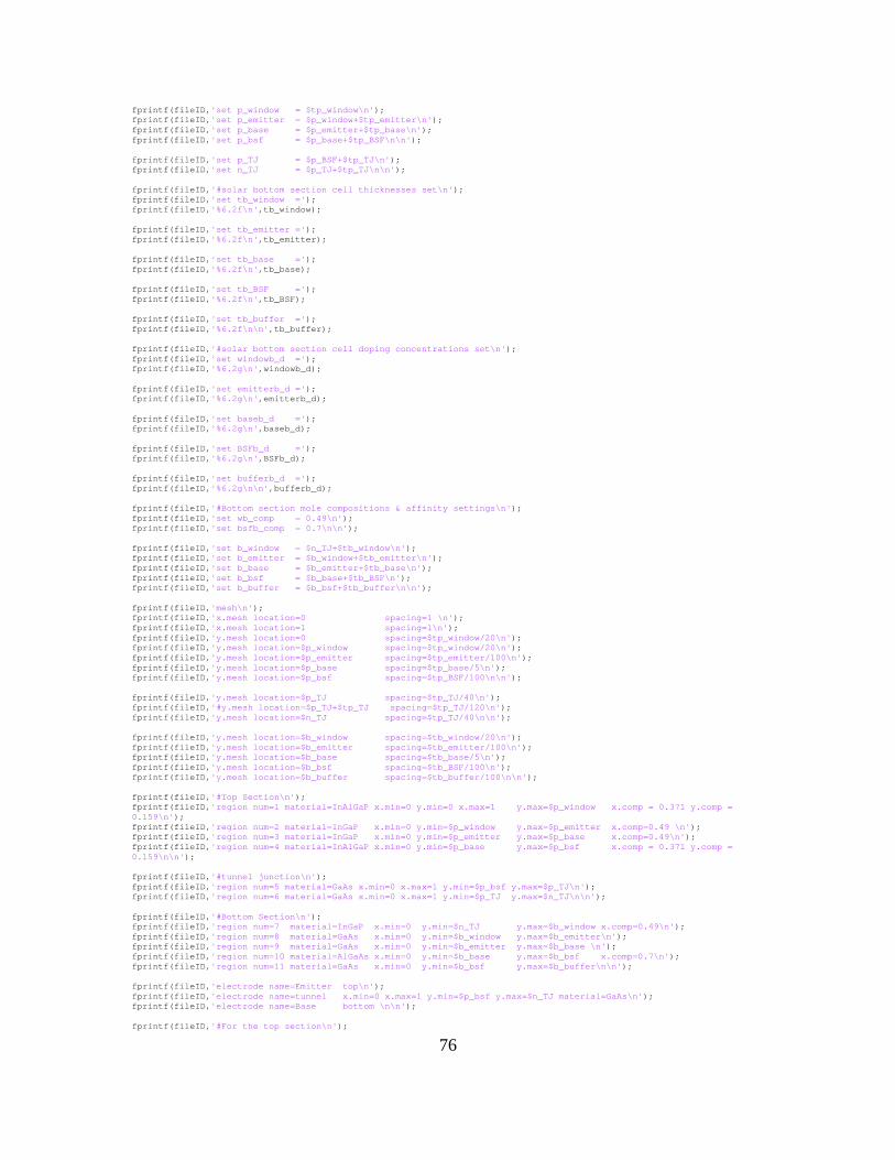
76
fprintf(fileID,'set p_window = $tp_window\n'); fprintf(fileID,'set p_emitter = $p_window+$tp_emitter\n'); fprintf(fileID,'set p_base = $p_emitter+$tp_base\n'); fprintf(fileID,'set p_bsf = $p_base+$tp_BSF\n\n'); fprintf(fileID,'set p_TJ = $p_BSF+$tp_TJ\n'); fprintf(fileID,'set n_TJ = $p_TJ+$tp_TJ\n\n'); fprintf(fileID,'#solar bottom section cell thicknesses set\n'); fprintf(fileID,'set tb_window ='); fprintf(fileID,'%6.2f\n',tb_window); fprintf(fileID,'set tb_emitter ='); fprintf(fileID,'%6.2f\n',tb_emitter); fprintf(fileID,'set tb_base ='); fprintf(fileID,'%6.2f\n',tb_base); fprintf(fileID,'set tb_BSF ='); fprintf(fileID,'%6.2f\n',tb_BSF); fprintf(fileID,'set tb_buffer ='); fprintf(fileID,'%6.2f\n\n',tb_buffer); fprintf(fileID,'#solar bottom section cell doping concentrations set\n'); fprintf(fileID,'set windowb_d ='); fprintf(fileID,'%6.2g\n',windowb_d); fprintf(fileID,'set emitterb_d ='); fprintf(fileID,'%6.2g\n',emitterb_d); fprintf(fileID,'set baseb_d ='); fprintf(fileID,'%6.2g\n',baseb_d); fprintf(fileID,'set BSFb_d ='); fprintf(fileID,'%6.2g\n',BSFb_d); fprintf(fileID,'set bufferb_d ='); fprintf(fileID,'%6.2g\n\n',bufferb_d); fprintf(fileID,'#Bottom section mole compositions & affinity settings\n'); fprintf(fileID,'set wb_comp = 0.49\n'); fprintf(fileID,'set bsfb_comp = 0.7\n\n'); fprintf(fileID,'set b_window = $n_TJ+$tb_window\n'); fprintf(fileID,'set b_emitter = $b_window+$tb_emitter\n'); fprintf(fileID,'set b_base = $b_emitter+$tb_base\n'); fprintf(fileID,'set b_bsf = $b_base+$tb_BSF\n'); fprintf(fileID,'set b_buffer = $b_bsf+$tb_buffer\n\n'); fprintf(fileID,'mesh\n'); fprintf(fileID,'x.mesh location=0 spacing=1 \n'); fprintf(fileID,'x.mesh location=1 spacing=1\n'); fprintf(fileID,'y.mesh location=0 spacing=$tp_window/20\n'); fprintf(fileID,'y.mesh location=$p_window spacing=$tp_window/20\n'); fprintf(fileID,'y.mesh location=$p_emitter spacing=$tp_emitter/100\n'); fprintf(fileID,'y.mesh location=$p_base spacing=$tp_base/5\n'); fprintf(fileID,'y.mesh location=$p_bsf spacing=$tp_BSF/100\n\n'); fprintf(fileID,'y.mesh location=$p_TJ spacing=$tp_TJ/40\n'); fprintf(fileID,'#y.mesh location=$p_TJ+$tp_TJ spacing=$tp_TJ/120\n'); fprintf(fileID,'y.mesh location=$n_TJ spacing=$tp_TJ/40\n\n'); fprintf(fileID,'y.mesh location=$b_window spacing=$tb_window/20\n'); fprintf(fileID,'y.mesh location=$b_emitter spacing=$tb_emitter/100\n'); fprintf(fileID,'y.mesh location=$b_base spacing=$tb_base/5\n'); fprintf(fileID,'y.mesh location=$b_bsf spacing=$tb_BSF/100\n'); fprintf(fileID,'y.mesh location=$b_buffer spacing=$tb_buffer/100\n\n'); fprintf(fileID,'#Top Section\n'); fprintf(fileID,'region num=1 material=InAlGaP x.min=0 y.min=0 x.max=1 y.max=$p_window x.comp = 0.371 y.comp = 0.159\n'); fprintf(fileID,'region num=2 material=InGaP x.min=0 y.min=$p_window y.max=$p_emitter x.comp=0.49 \n'); fprintf(fileID,'region num=3 material=InGaP x.min=0 y.min=$p_emitter y.max=$p_base x.comp=0.49\n'); fprintf(fileID,'region num=4 material=InAlGaP x.min=0 y.min=$p_base y.max=$p_bsf x.comp = 0.371 y.comp = 0.159\n\n'); fprintf(fileID,'#tunnel junction\n'); fprintf(fileID,'region num=5 material=GaAs x.min=0 x.max=1 y.min=$p_bsf y.max=$p_TJ\n'); fprintf(fileID,'region num=6 material=GaAs x.min=0 x.max=1 y.min=$p_TJ y.max=$n_TJ\n\n'); fprintf(fileID,'#Bottom Section\n'); fprintf(fileID,'region num=7 material=InGaP x.min=0 y.min=$n_TJ y.max=$b_window x.comp=0.49\n'); fprintf(fileID,'region num=8 material=GaAs x.min=0 y.min=$b_window y.max=$b_emitter\n'); fprintf(fileID,'region num=9 material=GaAs x.min=0 y.min=$b_emitter y.max=$b_base \n'); fprintf(fileID,'region num=10 material=AlGaAs x.min=0 y.min=$b_base y.max=$b_bsf x.comp=0.7\n'); fprintf(fileID,'region num=11 material=GaAs x.min=0 y.min=$b_bsf y.max=$b_buffer\n\n'); fprintf(fileID,'electrode name=Emitter top\n'); fprintf(fileID,'electrode name=tunnel x.min=0 x.max=1 y.min=$p_bsf y.max=$n_TJ material=GaAs\n'); fprintf(fileID,'electrode name=Base bottom \n\n'); fprintf(fileID,'#For the top section\n');
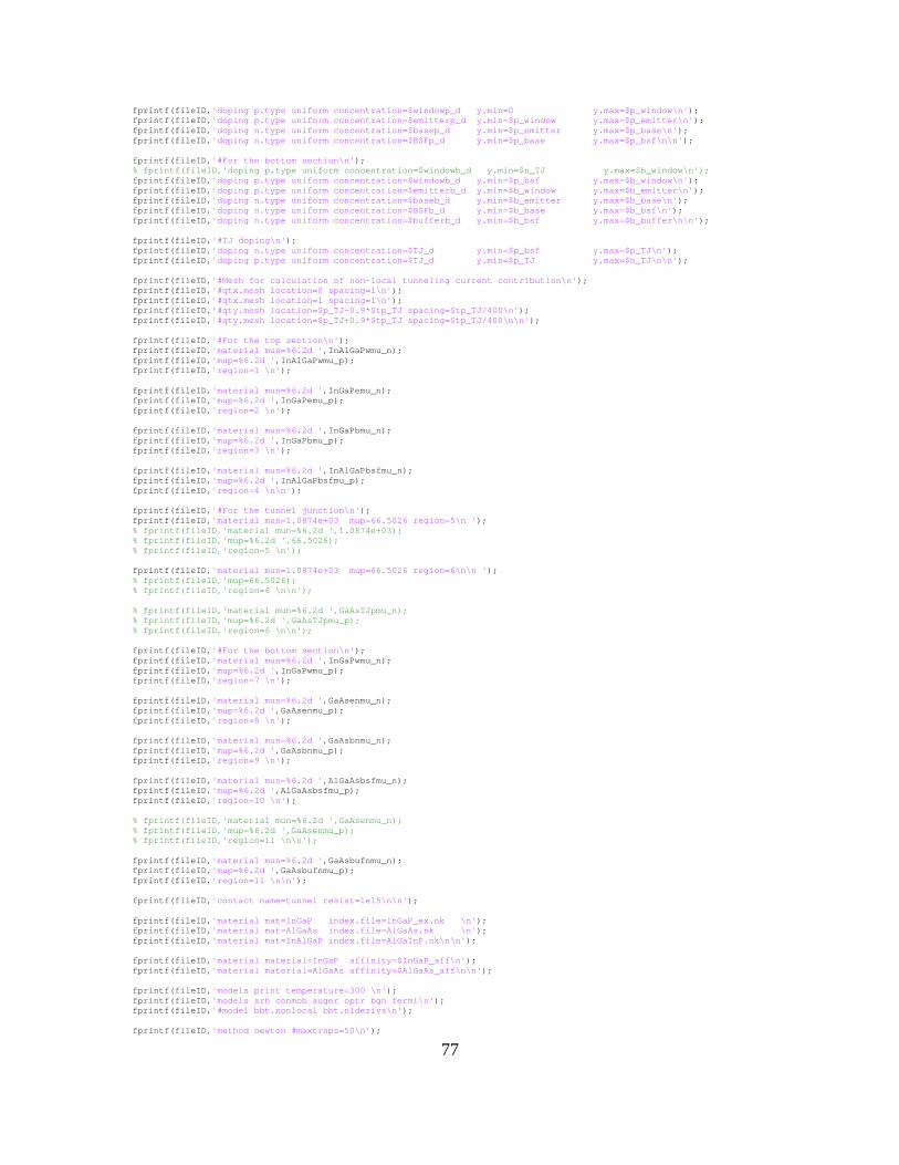
77
fprintf(fileID,'doping p.type uniform concentration=$windowp_d y.min=0 y.max=$p_window\n'); fprintf(fileID,'doping p.type uniform concentration=$emitterp_d y.min=$p_window y.max=$p_emitter\n'); fprintf(fileID,'doping n.type uniform concentration=$basep_d y.min=$p_emitter y.max=$p_base\n'); fprintf(fileID,'doping n.type uniform concentration=$BSFp_d y.min=$p_base y.max=$p_bsf\n\n'); fprintf(fileID,'#For the bottom section\n'); % fprintf(fileID,'doping p.type uniform concentration=$windowb_d y.min=$n_TJ y.max=$b_window\n'); fprintf(fileID,'doping p.type uniform concentration=$windowb_d y.min=$p_bsf y.max=$b_window\n'); fprintf(fileID,'doping p.type uniform concentration=$emitterb_d y.min=$b_window y.max=$b_emitter\n'); fprintf(fileID,'doping n.type uniform concentration=$baseb_d y.min=$b_emitter y.max=$b_base\n'); fprintf(fileID,'doping n.type uniform concentration=$BSFb_d y.min=$b_base y.max=$b_bsf\n'); fprintf(fileID,'doping n.type uniform concentration=$bufferb_d y.min=$b_bsf y.max=$b_buffer\n\n'); fprintf(fileID,'#TJ doping\n'); fprintf(fileID,'doping n.type uniform concentration=$TJ_d y.min=$p_bsf y.max=$p_TJ\n'); fprintf(fileID,'doping p.type uniform concentration=$TJ_d y.min=$p_TJ y.max=$n_TJ\n\n'); fprintf(fileID,'#Mesh for calculation of non-local tunneling current contribution\n'); fprintf(fileID,'#qtx.mesh location=0 spacing=1\n'); fprintf(fileID,'#qtx.mesh location=1 spacing=1\n'); fprintf(fileID,'#qty.mesh location=$p_TJ-0.9*$tp_TJ spacing=$tp_TJ/400\n'); fprintf(fileID,'#qty.mesh location=$p_TJ+0.9*$tp_TJ spacing=$tp_TJ/400\n\n'); fprintf(fileID,'#For the top section\n'); fprintf(fileID,'material mun=%6.2d ',InAlGaPwmu_n); fprintf(fileID,'mup=%6.2d ',InAlGaPwmu_p); fprintf(fileID,'region=1 \n'); fprintf(fileID,'material mun=%6.2d ',InGaPemu_n); fprintf(fileID,'mup=%6.2d ',InGaPemu_p); fprintf(fileID,'region=2 \n'); fprintf(fileID,'material mun=%6.2d ',InGaPbmu_n); fprintf(fileID,'mup=%6.2d ',InGaPbmu_p); fprintf(fileID,'region=3 \n'); fprintf(fileID,'material mun=%6.2d ',InAlGaPbsfmu_n); fprintf(fileID,'mup=%6.2d ',InAlGaPbsfmu_p); fprintf(fileID,'region=4 \n\n'); fprintf(fileID,'#For the tunnel junction\n'); fprintf(fileID,'material mun=1.0874e+03 mup=66.5026 region=5\n '); % fprintf(fileID,'material mun=%6.2d ',1.0874e+03); % fprintf(fileID,'mup=%6.2d ',66.5026); % fprintf(fileID,'region=5 \n'); fprintf(fileID,'material mun=1.0874e+03 mup=66.5026 region=6\n\n '); % fprintf(fileID,'mup=66.5026); % fprintf(fileID,'region=6 \n\n'); % fprintf(fileID,'material mun=%6.2d ',GaAsTJpmu_n); % fprintf(fileID,'mup=%6.2d ',GaAsTJpmu_p); % fprintf(fileID,'region=6 \n\n'); fprintf(fileID,'#For the bottom section\n'); fprintf(fileID,'material mun=%6.2d ',InGaPwmu_n); fprintf(fileID,'mup=%6.2d ',InGaPwmu_p); fprintf(fileID,'region=7 \n'); fprintf(fileID,'material mun=%6.2d ',GaAsenmu_n); fprintf(fileID,'mup=%6.2d ',GaAsenmu_p); fprintf(fileID,'region=8 \n'); fprintf(fileID,'material mun=%6.2d ',GaAsbnmu_n); fprintf(fileID,'mup=%6.2d ',GaAsbnmu_p); fprintf(fileID,'region=9 \n'); fprintf(fileID,'material mun=%6.2d ',AlGaAsbsfmu_n); fprintf(fileID,'mup=%6.2d ',AlGaAsbsfmu_p); fprintf(fileID,'region=10 \n'); % fprintf(fileID,'material mun=%6.2d ',GaAsenmu_n); % fprintf(fileID,'mup=%6.2d ',GaAsenmu_p); % fprintf(fileID,'region=11 \n\n'); fprintf(fileID,'material mun=%6.2d ',GaAsbufnmu_n); fprintf(fileID,'mup=%6.2d ',GaAsbufnmu_p); fprintf(fileID,'region=11 \n\n'); fprintf(fileID,'contact name=tunnel resist=1e15\n\n'); fprintf(fileID,'material mat=InGaP index.file=InGaP_ex.nk \n'); fprintf(fileID,'material mat=AlGaAs index.file=AlGaAs.nk \n'); fprintf(fileID,'material mat=InAlGaP index.file=AlGaInP.nk\n\n'); fprintf(fileID,'material material=InGaP affinity=$InGaP_aff\n'); fprintf(fileID,'material material=AlGaAs affinity=$AlGaAs_aff\n\n'); fprintf(fileID,'models print temperature=300 \n'); fprintf(fileID,'models srh conmob auger optr bgn fermi\n'); fprintf(fileID,'#model bbt.nonlocal bbt.nlderivs\n'); fprintf(fileID,'method newton #maxtraps=50\n');

78
fprintf(fileID,'output con.band val.band charge opt.intens \n\n'); fprintf(fileID,'beam num=1 AM0 x.origin=0.5 y.origin=-1.0 angle=90\n\n'); fprintf(fileID,'solve init\n'); fprintf(fileID,'save outfile=equilibriumSimpleTJ%d.str\n\n',i); fprintf(fileID,'solve b1=0.9\n\n'); fprintf(fileID,'save outf=shortcircuitSimpleTJ%d.str\n\n',i); fprintf(fileID,'log outfileTJ=forward_IVSimpleTJ%d.log\n',i); fprintf(fileID,'solve name=Emitter vEmitter=0.0 vstep=0.05 vfinal=0.2\n\n'); fprintf(fileID,'save outfile=for_02SimpleTJ%d.str\n\n',i); fprintf(fileID,'solve name=Emitter vEmitter=0.2 vstep=0.01 vfinal=3.5\n'); fprintf(fileID,'log off\n\n'); fprintf(fileID,'save outfile=forSimpleTJ%d.str\n\n',i); fprintf(fileID,'quit\n\n'); fclose(fileID); end
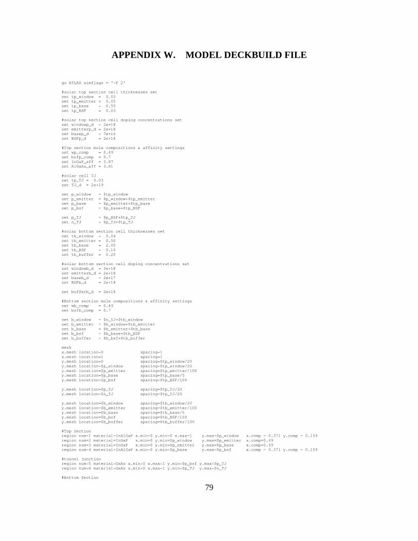
79
APPENDIX W. MODEL DECKBUILD FILE
go ATLAS simflags = "-P 2" #solar top section cell thicknesses set set tp_window = 0.03 set tp_emitter = 0.05 set tp_base = 0.55 set tp_BSF = 0.03 #solar top section cell doping concentrations set set windowp_d = 2e+18 set emitterp_d = 2e+18 set basep_d = 7e+16 set BSFp_d = 2e+18 #Top section mole compositions & affinity settings set wp_comp = 0.49 set bsfp_comp = 0.7 set InGaP_aff = 3.87 set AlGaAs_aff = 3.81 #solar cell TJ set tp_TJ = 0.03 set TJ_d = 2e+19 set p_window = $tp_window set p_emitter = $p_window+$tp_emitter set p_base = $p_emitter+$tp_base set p_bsf = $p_base+$tp_BSF set p_TJ = $p_BSF+$tp_TJ set n_TJ = $p_TJ+$tp_TJ #solar bottom section cell thicknesses set set tb_window = 0.04 set tb_emitter = 0.50 set tb_base = 2.05 set tb_BSF = 0.10 set tb_buffer = 0.20 #solar bottom section cell doping concentrations set set windowb_d = 3e+18 set emitterb_d = 2e+18 set baseb_d = 2e+17 set BSFb_d = 2e+18 set bufferb_d = 2e+18 #Bottom section mole compositions & affinity settings set wb_comp = 0.49 set bsfb_comp = 0.7 set b_window = $n_TJ+$tb_window set b_emitter = $b_window+$tb_emitter set b_base = $b_emitter+$tb_base set b_bsf = $b_base+$tb_BSF set b_buffer = $b_bsf+$tb_buffer mesh x.mesh location=0 spacing=1 x.mesh location=1 spacing=1 y.mesh location=0 spacing=$tp_window/20 y.mesh location=$p_window spacing=$tp_window/20 y.mesh location=$p_emitter spacing=$tp_emitter/100 y.mesh location=$p_base spacing=$tp_base/5 y.mesh location=$p_bsf spacing=$tp_BSF/100 y.mesh location=$p_TJ spacing=$tp_TJ/20 y.mesh location=$n_TJ spacing=$tp_TJ/20 y.mesh location=$b_window spacing=$tb_window/20 y.mesh location=$b_emitter spacing=$tb_emitter/100 y.mesh location=$b_base spacing=$tb_base/5 y.mesh location=$b_bsf spacing=$tb_BSF/100 y.mesh location=$b_buffer spacing=$tb_buffer/100 #Top Section region num=1 material=InAlGaP x.min=0 y.min=0 x.max=1 y.max=$p_window x.comp = 0.371 y.comp = 0.159 region num=2 material=InGaP x.min=0 y.min=$p_window y.max=$p_emitter x.comp=0.49 region num=3 material=InGaP x.min=0 y.min=$p_emitter y.max=$p_base x.comp=0.49 region num=4 material=InAlGaP x.min=0 y.min=$p_base y.max=$p_bsf x.comp = 0.371 y.comp = 0.159 #tunnel junction region num=5 material=GaAs x.min=0 x.max=1 y.min=$p_bsf y.max=$p_TJ region num=6 material=GaAs x.min=0 x.max=1 y.min=$p_TJ y.max=$n_TJ #Bottom Section

80
region num=7 material=InGaP x.min=0 y.min=$n_TJ y.max=$b_window x.comp=0.49 region num=8 material=GaAs x.min=0 y.min=$b_window y.max=$b_emitter region num=9 material=GaAs x.min=0 y.min=$b_emitter y.max=$b_base region num=10 material=AlGaAs x.min=0 y.min=$b_base y.max=$b_bsf x.comp=0.7 region num=11 material=GaAs x.min=0 y.min=$b_bsf y.max=$b_buffer electrode name=Emitter top electrode name=tunnel x.min=0 x.max=1 y.min=$p_bsf y.max=$n_TJ material=GaAs electrode name=Base bottom #For the top section doping p.type uniform concentration=$windowp_d y.min=0 y.max=$p_window doping p.type uniform concentration=$emitterp_d y.min=$p_window y.max=$p_emitter doping n.type uniform concentration=$basep_d y.min=$p_emitter y.max=$p_base doping n.type uniform concentration=$BSFp_d y.min=$p_base y.max=$p_bsf #For the bottom section doping p.type uniform concentration=$windowb_d y.min=$p_bsf y.max=$b_window doping p.type uniform concentration=$emitterb_d y.min=$b_window y.max=$b_emitter doping n.type uniform concentration=$baseb_d y.min=$b_emitter y.max=$b_base doping n.type uniform concentration=$BSFb_d y.min=$b_base y.max=$b_bsf doping n.type uniform concentration=$bufferb_d y.min=$b_bsf y.max=$b_buffer #TJ doping doping n.type uniform concentration=$TJ_d y.min=$p_bsf y.max=$p_TJ doping p.type uniform concentration=$TJ_d y.min=$p_TJ y.max=$n_TJ #For the top section material mun=1.06e+02 mup=5.10e+01 region=1 material mun=4.05e+02 mup=6.69e+01 region=2 material mun=6.76e+02 mup=1.52e+02 region=3 material mun=1.06e+02 mup=5.10e+01 region=4 #For the tunnel junction material mun=1.32e+03 mup=8.33e+01 region=5 material mun=1.32e+03 mup=8.33e+01 region=6 #For the bottom section material mun=3.64e+02 mup=5.53e+01 region=7 material mun=2.29e+03 mup=1.48e+02 region=8 material mun=3.91e+03 mup=2.42e+02 region=9 material mun=3.98e+02 mup=5.43e+01 region=10 material mun=2.29e+03 mup=1.48e+02 region=11 contact name=tunnel resist=1e15 material mat=InGaP index.file=InGaP_ex.nk material mat=AlGaAs index.file=AlGaAs.nk material mat=InAlGaP index.file=AlGaInP.nk material material=InGaP affinity=$InGaP_aff material material=AlGaAs affinity=$AlGaAs_aff models print temperature=300 models srh conmob auger optr bgn fermi method newton output con.band val.band charge opt.intens beam num=1 AM0 x.origin=0.5 y.origin=-1.0 angle=90 solve init save outfile=equilibrium.str solve b1=0.9 save outf=shortcircuit.str tonyplot shortcircuit.str log outfileTJ=forward_IV.log solve name=Emitter vEmitter=0.0 vstep=0.05 vfinal=0.2 save outfile=for_02.str solve name=Emitter vEmitter=0.2 vstep=0.01 vfinal=3.5 log off save outfile=for.str tonyplot equilibrium.str for.str for_02.str tonyplot forward_IV.log quit
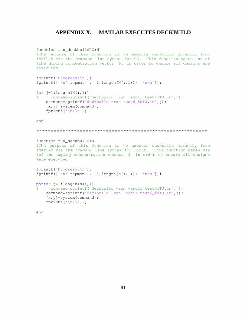
81
APPENDIX X. MATLAB EXECUTES DECKBUILD
function run_deckbuildPC(N) %The purpose of this function is to execute deckbuild directly from %MATLAB via the command line syntax for PC. This function makes use of %the doping concentration vector, N, in order to ensure all designs are %executed fprintf('Progress:\n'); fprintf(['\n' repmat('.',1,length(N(:,1))) '\n\n']); for j=1:length(N(:,1)) % command=sprintf("deckbuild -run -ascii test%dTJ.in",j); command=sprintf("deckbuild -run test6_%dTJ.in",j); [x,y]=system(command); fprintf('\b|\n'); end *********************************************************** function run_deckbuild(N) %The purpose of this function is to execute deckbuild directly from %MATLAB via the command line syntax for Linux. This function makes use %of the doping concentration vector, N, in order to ensure all designs %are executed fprintf('Progress:\n'); fprintf(['\n' repmat('.',1,length(N(:,1))) '\n\n']); parfor j=1:length(N(:,1)) % command=sprintf("deckbuild -run -ascii test%dTJ.in",j); command=sprintf("deckbuild -run -ascii test6_%dTJ.in",j); [x,y]=system(command); fprintf('\b|\n'); end

82
THIS PAGE INTENTIONALLY LEFT BLANK
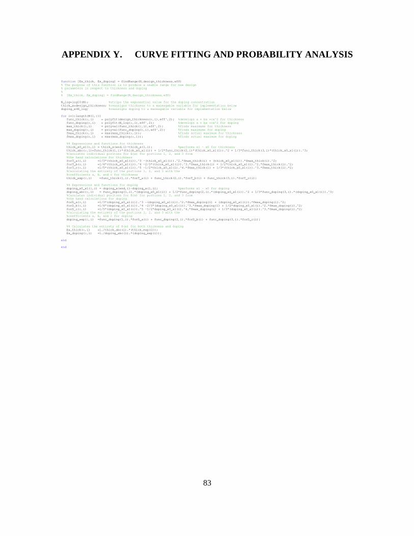
83
APPENDIX Y. CURVE FITTING AND PROBABILITY ANALYSIS
function [Ex_thick, Ex_doping] = findRange(N,design_thickness,eff) % The purpose of this function is to produce a usable range for new design % parameters in respect to thickness and doping % % [Ex_thick, Ex_doping] = findRange(N,design_thickness,eff) N_log=log10(N); %strips the exponential value for the doping concentration thick_x=design_thickness; %reassigns thickness to a maneagable variable for implementation below doping_x=N_log; %reassigns doping to a maneagable variable for implementation below for i=1:length(N(1,:)) func_thick(:,i) = polyfit(design_thickness(:,i),eff',2); %develops a + bx +cx^2 for thickness func_doping(:,i) = polyfit(N_log(:,i),eff',2); %develops a + bx +cx^2 for doping max_thick(:,i) = polyval(func_thick(:,i),eff',2); %finds maximums for thickness max_doping(:,i) = polyval(func_doping(:,i),eff',2); %finds maximums for doping fmax_thick(:,i) = max(max_thick(:,i)); %finds actual maximum for thickness fmax_doping(:,i) = max(max_doping(:,i)); %finds actual maximum for doping %% Expressions and functions for thickness thick_x0_x1(:,i) = thick_x(end,i)-thick_x(1,i); %performs x1 - x0 for thickness thick_abc(:,i)=func_thick(1,i)*(thick_x0_x1(i)) + 1/2*func_thick(2,i)*(thick_x0_x1(i)).^2 + 1/3*func_thick(3,i)*(thick_x0_x1(i)).^3; %Caculates individual poritons for E(x) for portions 1, 2, and 3 from %the hand calculations for thickness forT_a(:,i) =1/3*(thick_x0_x1(i)).^3 -(thick_x0_x1(i)).^2.*fmax_thick(i) + (thick_x0_x1(i)).*fmax_thick(i).^2; forT_b(:,i) =1/4*(thick_x0_x1(i)).^4 -2/3*(thick_x0_x1(i)).^3.*fmax_thick(i) + 1/2*thick_x0_x1(i).^2.*fmax_thick(i).^2; forT_c(:,i) =1/5*(thick_x0_x1(i)).^5 -1/2*thick_x0_x1(i).^4.*fmax_thick(i) + 1/3*(thick_x0_x1(i)).^3.*fmax_thick(i).*2; %Calculating the entirety of the portions 1, 2, and 3 with the %coefficients a, b, and c for thickness thick_exp(:,i) =func_thick(1,i).*forT_a(i) + func_thick(2,i).*forT_b(i) + func_thick(3,i).*forT_c(i); %% Expressions and functions for doping doping_x0_x1(:,i) = doping_x(end,i)-doping_x(1,i); %performs x1 - x0 for doping doping_abc(:,i) = func_doping(1,i).*(doping_x0_x1(i)) + 1/2*func_doping(2,i).*(doping_x0_x1(i)).^2 + 1/3*func_doping(3,i).*(doping_x0_x1(i)).^3; %Caculates individual poritons for E(x) for portions 1, 2, and 3 from %the hand calculations for doping forD_a(:,i) =1/3*(doping_x0_x1(i)).^3 -(doping_x0_x1(i)).^2.*fmax_doping(i) + (doping_x0_x1(i)).*fmax_doping(i).^2; forD_b(:,i) =1/4*(doping_x0_x1(i)).^4 -2/3*(doping_x0_x1(i)).^3.*fmax_doping(i) + 1/2*doping_x0_x1(i).^2.*fmax_doping(i).^2; forD_c(:,i) =1/5*(doping_x0_x1(i)).^5 -1/2*doping_x0_x1(i).^4.*fmax_doping(i) + 1/3*(doping_x0_x1(i)).^3.*fmax_doping(i).*2; %Calculating the entirety of the portions 1, 2, and 3 with the %coefficients a, b, and c for doping doping_exp(:,i) =func_doping(1,i).*forD_a(i) + func_doping(2,i).*forD_b(i) + func_doping(3,i).*forD_c(i); %% Calculates the entirety of E(x) for both thickness and doping Ex_thick(:,i) =1./thick_abc(i).*(thick_exp(i)); Ex_doping(:,i) =1./doping_abc(i).*(doping_exp(i)); end end

84
THIS PAGE INTENTIONALLY LEFT BLANK
85
LIST OF REFERENCES
[1] J. S. Walsh, “Optimization of multi-junction solar cells for space applications modeled with Silvaco ATLAS,” M. S. thesis, Dept. Elec. Eng., NPS, Monterey, CA, USA, 2018. [Online]. Available: http://hdl.handle.net/10945/59615
[2] P. Michalopoulos, “A novel approach for the development and optimization of
state-of-the-art photovoltaic devices using Silvaco,” M. S. thesis, Dept. Elec. Eng, NPS, Monterey, CA, USA, 2003. [Online]. Available: https://calhoun.nps.edu/handle/10945/5609
[3] R. Kilway, “Five-junction solar cell optimization using Silvaco ATLAS,” Dept.
Elec. Eng., NPS, Monterey, CA, USA, 2017. [Online]. Available: https://calhoun.nps.edu/handle/10945/56146
[4] S. Pueschel, “Optimization of an advanced multi-junction solar-cell design for
space environments (AM0) using nearly orthogonal Latin hypercubes,” M. S. thesis, Dept. Op. Res., NPS, Monterey, CA, USA, 2017. [Online]. Available: http://hdl.handle.net/10945/55521
[5] B.G. Streetman and S. K. Banerjee, Solid State Electronic Devices, Upper Saddle
River, NJ, USA: Prentice-Hall , 2009. [6] M. Lundstrom, “Introduction to Photovoltaics,” class notes for NCN Summer
School, Purdue University, West Lafayette, IN, USA , 2011. [Online]. Available https://nanohub.org/resources/11884/download/2011.07.20-NCN-SC01-Lundstrom.pdf
[7] S. M. Sze and K. K. Ng, Physics of Semiconductor Devices, Hoboken, NJ, USA:
John Wiley and Sons , 2007. [8] M. R. Lueck, C. L. Andre, A. J. Pitera, M. L. Lee, A. Fitzgerald, and S. A. Ringel,
“Dual-junction GaInP/GaAs solar cells grown on metamorphic SiGe/Si substrates with high open circuit voltage,” IEEE Electron Device Letters, vol. 27, no. 3, pp. 142–144, 2006.
[9] A. D. MacCalman, H. Vieira, and T. Lucas, “Second-order nearly orthogonal
Latin hypercubes for exploring stochastic simulations,” Journal of Simulation, vol. 11, no. 2, pp. 137–150, May 2017.
[10] RubyInstaller. 2019. [Online] Available: https://rubyinstaller.org/

86
THIS PAGE INTENTIONALLY LEFT BLANK

87
INITIAL DISTRIBUTION LIST
1. Defense Technical Information Center Ft. Belvoir, Virginia 2. Dudley Knox Library Naval Postgraduate School Monterey, California
Copyright © 2022 FDOKUMEN