
Optimal bus sizing in migration of processor design
40
1 Optimal Bus Sizing in Migration of Processor Design Shmuel Wimer¹, Shay Michaely 2 , Konstantin Moiseev 2 , Avinoam Kolodny 2 1. Intel Corporation, Israel Development Center, Haifa, Israel 2. Electrical Engineering Department, Technion, Haifa, Israel Abstract The effect of wire delay on circuit timing typically increases when an existing layout is migrated to a new generation of process technology, because wire resistance and cross capacitances do not scale well. Hence, careful sizing and spacing of wires is an important task in migration of a processor to next generation technology. In this paper, timing optimization of signal buses is performed by resizing and spacing individual bus wires, while the area of the whole bus structure is regarded as a fixed constraint. Four different objective functions are defined and their usefulness is discussed in the context of the layout migration process. The paper presents solutions for the respective optimization problems and analyzes their properties. In an optimally-tuned bus layout, after optimizing the most critical signal delay, all signal delays (or slacks) are equal. The optimal solution of the MinMax problem is always bounded by the solution of the corresponding sum-of-delays problem. An iterative algorithm to find the optimally-tuned bus layout is presented. Examples of solutions are shown, and design implications are derived and discussed.
-
Upload
independent -
Category
Documents
-
view
2 -
download
0
Transcript of Optimal bus sizing in migration of processor design

1
Optimal Bus Sizing in Migration of Processor Design
Shmuel Wimer¹, Shay Michaely2, Konstantin Moiseev2, Avinoam Kolodny2
1. Intel Corporation, Israel Development Center, Haifa, Israel 2. Electrical Engineering Department, Technion, Haifa, Israel
Abstract
The effect of wire delay on circuit timing typically increases when an existing
layout is migrated to a new generation of process technology, because wire
resistance and cross capacitances do not scale well. Hence, careful sizing and
spacing of wires is an important task in migration of a processor to next
generation technology. In this paper, timing optimization of signal buses is
performed by resizing and spacing individual bus wires, while the area of the
whole bus structure is regarded as a fixed constraint. Four different objective
functions are defined and their usefulness is discussed in the context of the
layout migration process. The paper presents solutions for the respective
optimization problems and analyzes their properties. In an optimally-tuned bus
layout, after optimizing the most critical signal delay, all signal delays (or
slacks) are equal. The optimal solution of the MinMax problem is always
bounded by the solution of the corresponding sum-of-delays problem. An
iterative algorithm to find the optimally-tuned bus layout is presented.
Examples of solutions are shown, and design implications are derived and
discussed.

2
Introduction
Interconnect delays have become dominant in CMOS VLSI digital systems as
a result of technology scaling [ 1] [2]. In recent generations, wire resistance
and cross-capacitance between adjacent wires have become increasingly
important in their effect on signal delay. For a given metal layer, wire
resistance and cross-capacitance depend on wire width and inter-wire spacing,
respectively. Allocation of wire widths and spaces for bus structures under a
total area constraint is an important problem in process migration of existing
mask layouts (also known as “process shifting”), which often produces
excessive wire delays in the new layout. In state-of-the-art technology
migration, about 10% improvement in timing of buses is achievable by
judicious allocation of wire widths and inter-wire spaces. The strategy of
allocating widths and spaces to maximize performance in bus structures was
proposed in [ 3] without formal analysis and solution. The nature of this
problem allows tradeoff between the resistance of a wire and its coupling
capacitances to adjacent wires, by increasing wire width while reducing
spaces, or vice versa. Wire resistance affects only the delay of the signal
carried by the wire, while coupling capacitances affect the delays of both the
wire and its neighbors. For multiple nets, the optimal solution involves
simultaneous tradeoffs among all wires sharing a given common area.
The wire sizing problem has been addressed in [ 4] and [ 5] for a single wire and
for a single-net interconnect tree. Simultaneous wire sizing and driver sizing
has been presented in [ 6, 7]. The problem of sizing and spacing multiple nets
with consideration of coupling capacitance in global interconnect has been
addressed in [ 8], considering general tree structures for nets with fixed

3
terminals, without a total area constraint. The authors modeled coupling
between nets by converting cross-capacitance into an effective fringe
capacitance, which resulted in a decoupled delay model for each net. The
routing tree for each net was sized independently, using an algorithm based on
dynamic programming [ 9]. Coupling capacitance has been considered more
explicitly in the context of physical design algorithms for minimizing crosstalk
noise [ 4, 10, 11] or dynamic power [ 12]. The authors of [ 13] derived layout
guidelines and presented a simultaneous multiple-net spacing algorithm for area
minimization in general layouts under a noise-constraint.
This paper addresses the problem of simultaneously assigning widths and
spaces to n parallel wires, representing a bus or several interleaved busses, as
illustrated in Figure 1. Such geometry is commonly used in practice, and its
simplicity enables straightforward mathematical analysis. With given drivers,
load capacitances and timing requirements for the individual signals, wire
widths and spaces are allocated to maximize circuit speed. Note that driver
strengths, load capacitances and required arrival times are not necessarily
equal. The total sum of widths and spaces is a given constraint, representing
the total width available for the bus structure in the layout. The problem is
presented in the context of technology migration, but the same methods can be
used to optimize a initial design, not just a migrated one.
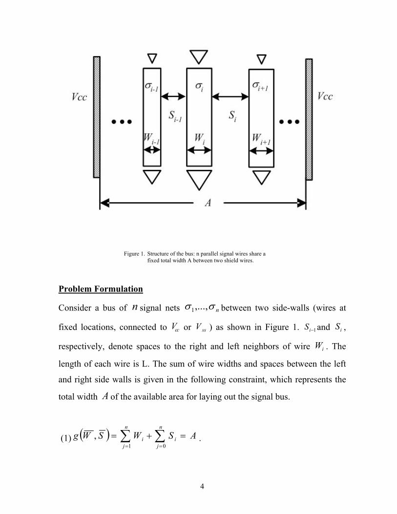
4
Figure 1. Structure of the bus: n parallel signal wires share a fixed total width A between two shield wires.
Problem Formulation
Consider a bus of n signal nets nσσ ,...,1 between two side-walls (wires at
fixed locations, connected to ccV or ssV ) as shown in Figure 1. 1−iS and iS ,
respectively, denote spaces to the right and left neighbors of wire iW . The
length of each wire is L. The sum of wire widths and spaces between the left
and right side walls is given in the following constraint, which represents the
total width A of the available area for laying out the signal bus.
(1) ( ) ASWSWgn
ji
n
ji =+= ∑∑
== 01, .

5
Another set of constraints on wire sizing is geometrical design rules, which are
imposed by the manufacturing technology. In modern processes of 90
nanometers and below, the width and the space of wires are bounded in some
range as follows:
(2) niSSS i ≤≤′′≤≤′ 0, , and
(3) niWWW i ≤≤′′≤≤′ 1, .
Delay model
Signal delays are expressed by an Elmore model using simple approximation
for capacitances. The delay of signal iσ can be calculated from the π-model
equivalent circuit shown in Figure 2, whereidR is the effective output
resistance of the driver,iwR is the wire resistance,
iwC is the wire area and
fringe capacitance, 1icC−
and icC are coupling capacitances to the right and left
neighboring signals, and il
C is the capacitive load presented by the receiver’s
input. Using technology parameters these can be expressed as isR WLRRi= ,
iw a i fC C LW C L= + and ic c iC k L S= , where aC is area capacitance coefficient,
fC is fringe capacitance coefficient, ck is a line-to-line coupling coefficient,
and sR is the metal sheet resistance. These are first-order approximations [ 14]
which capture the fundamental nature of the problem.

6
Figure 2. Equivalent circuit for calculating the ith signal delay
Under Elmore delay model, the delay i∆ of signal iσ from driver’s input to
receiver’s input is given as follows:
(4)
2
2 21 1
1 1
12
1 1 1 12 2
i i i i
i i
i d a i i d f d l a s
i i i is f s l d c s c
i i i i i i
R C LW D R C L R C C R L
MCF MCF MCF MCFR C L R LC R k L R k LW S S W S S
− −
− −
∆ = + + + + +
+ + + + +
Note that the cross-coupling capacitances between wires are multiplied by a
Miller Coupling Factor (MCF) [ 16] in the model equation. For nominal
delays, without delay uncertainty induced by crosstalk, MCF=1 is assumed.
This is valid in particular when adjacent wires are functionally interleaved,
such that simultaneous transitions of neighbor wires are avoided. If all wires
can switch simultaneously, the cross-capacitance terms are typically multiplied
by a uniform MCF of 2. For such a case, inter-wire tradeoffs would become
even more pronounced in optimizing the bus layout. In the remainder of this

7
paper we assume MCF=1. The coefficients of wire width and spaces in (4)
will be marked as edcba iiii ,,,, . The delay expression can be rearranged
as
(5) ( )
+×
++++=∆
− iiii
i
iiiii SSW
edWcbWaSW 11,
1.
Note that in (5) the coefficient e is not indexed since it encapsulates only
technology parameters, which are common to all delays. The other coefficients
are indexed since they include parameters related to the signal’s driver and
receiver.
Despite its simplicity, this Elmore-based modeling approach is widely used
as a high-fidelity estimator in practical interconnect optimizations. Although it
uses first-order capacitance approximations, and even though it does not
account for signal slope effects, it is effective in guiding the search towards
improved timing, as was verified by detailed circuit simulations on examples
below. A multiplicative factor of 0.7 is generally used to fit the Elmore model
with 50% signal delay. With more elaborate empirical parameter tuning, the
model accuracy can be improved further: In [ 15], good absolute accuracy
versus circuit simulation has been obtained by applying a parameter fitting
procedure to a similar wire delay model, where the cross-capacitances were
replaced by a fringing-field term.
Sensitivity of signal delay to wire width and spaces
Consider a single wire placed between two side-walls. The delay of the wire is

8
given by (5), with 1=i . Partial derivatives with respect to W1 and S1 are as
follows (note that the delay function is symmetrical in S variables, S0= S1):
(6) ( )1 121 1
1a c eW W∂∆
= − +∂
(7) 121 1 1
1 edS S W
∂∆= − + ∂
Omitting the index i=1, for each specific value of S the sensitivity to W is
zero at a certain point min( ( ), )W S∆ . This point is the minimum delay point for
the given value of S . Sensitivity to S decreases monotonically with increasing
of S and W .
In layout migration, wire width and spaces to neighbors cannot change
independently. The additional constraint applied to W and S is:
(8) 0 1W S S A+ + = , and therefore for fixed 1S :
(9)0SW ∂∆∂
−=∂∆∂ .
The sensitivities to both S and W are thus identical. An example is shown in
Figure 3 using 90 nanometer technology parameters for different driver
resistances – 100Ω , 500Ω and 1000Ω , driving a wire of 1000 microns length,
with load capacitance of 50 fF and the distance between walls is 1.5 microns.
Sensitivity to both W and S was calculated for values of W from 0 to 1.5 µm.
At the minimum delay point, sensitivity to wire width and spaces is zero,

9
because the effect of any change in wire resistance balances out with the
respective change in capacitances. A similar balance is obtained also when a
bus with multiple wires is optimized, as will be discussed below. For wide
buses, where inter-wire separation is large, the optimal width for each wire
depends mostly on values of driver resistance and load capacitance of the wire,
according to (8). This may be used as a first approximation for assigning
initial values to wire widths in bus optimization.
Figure 3: Delay sensitivity to width and space for a single wire

10
Timing Objectives for bus optimization
We are seeking wire width and space allocation yielding “optimal timing”.
The definition of optimality depends on the design scenario. In the following
we’ll define four commonly used timing objectives.
First objective aims at maximizing the total sum of slacks (same as
maximizing the average slack). Let iT be the required time of the signal iσ .
The objective is thus defined as follows:
(10) ( ) ( ) ∑∑= −=
+×
++++−=∆−=
n
i iiii
i
iiiii
n
iii SSW
edWcbWaTSWTSWf
1 111
11,, .
When required times are still undetermined, an objective of minimizing total
sum of delays is commonly used. Notice that from a mathematical point of
view this is equivalent to maximizing the first objective, since
(11) ( ) ( ) ( ) ∑∑==
+−=∆=n
ii
n
ii TSWfSWSWf
11
12 ,,, .
The term ∑=
n
iiT
1however is constant and doesn’t affect the optimization. In the
sequel we’ll discuss the minimization of total sum of delays 2f . Without loss
of generality the results are applicable to maximization of total slack 1f .
Both (10) and (11) are cumulative metrics, integrating the contribution of all
signal wires. These are useful objectives for design migration, where the goal
is to deliver overall timing speedup. The important factor in such a design
scenario is the average speedup, which is well reflected by (10) and (11).

11
When tuning of critical signals is of interest, the design scenario calls for
MinMax optimization problems. Hence, a third objective is to minimize the
worst slack among all signals, expressed by 3f below. Note that we
exchanged the terms of the slack for the sake of mathematical convenience.
(12) ( ) ( ) iini
TSWSWf −∆=≤≤
,, max1
3 .
A fourth objective aims at minimizing the delay of the slowest signal in the
bus. It can be used when timing constraints are not known yet. The
corresponding objective function is:
(13) ( ) ( ) SWSWf ini
,, max1
4 ∆=≤≤
.
In the following we’ll explore the optimization of the objective functions
1f through 4f by varying the widths and spaces of the bus wires. We first
note that all the objectives have a global optimum since the underlying
problems are all convex or concave. The convexity proof is given in Appendix
A. Additional useful properties of the underlying optimization that suggest
efficient solutions are discussed below. Let us ignore design rules (2) and (3)
for the sake of easing the analysis. These do not change the nature of the
problem.
Optimizing total sum of slacks or delays
We are aiming at minimizing (11) subject to (1). In order to find the minimum
of 2f under g constraint, let us calculate partial derivatives.

12
(14) niSSW
eWca
Wf
iiii
ii
i
,...,1,11
122
2 =
+−−=
∂∂
−
(15) niWW
eddSS
f
iiii
ii
,...,0,111
112
2 =
+++−=
∂∂
++
(16) niWg
i
≤≤=∂∂ 1,1 , (17) ni
Sg
i
≤≤=∂∂ 0,1
At minimum there exists some real numberλ (Lagrange multiplier),
satisfying gf ∇=∇ λ1 . Rearranging and substituting yields the
following:
(18) niSS
ecW
aii
ii
i ,...,1,111
12 =
++−=
−
λ
(19) niWW
eddS ii
iii
,...,0,111
112 =
+++−=
++λ
We define ∞== +10 nWW to represent a sidewall connected to power or
ground. The above equations plus the area constraint equation (1) impose
2n+2 algebraic equations in 2n+2 variables nn SSWW 01 ,,λ .
The equations to obtain the maximum of total sum of slacks are identical to
(18) and (19). Similar arguments hold, except that minimum is replaced by
maximum and convexity by concavity.

13
Minimizing maximal delays and negative slack: MinMax problems
Objective functions (12) and (13) dealing with worst delay and slack are not
differentiable. Therefore, the respective MinMax optimization problems
cannot be solved analytically. Although general convex programming or
Lagrange relaxation [ 7] can be employed, we propose a solution approach
based on the following properties of these specific problems, yielding an
efficient iterative solution with guaranteed convergence.
Theorem 1 (necessary condition): In the optimal solution of minimizing the
maximal delay in (13) (worst slack in (12)) subject to the area constraint (1),
all the delays (slacks) are equal.
Proof: Let us prove the case of delays. Assume on the contrary that the above
assertion doesn’t hold. Namely, in the optimal solution there exists a wire
i whose associated delay is greater than all others. If there are few maximal
ones, pick one having a neighbor with a smaller delay. Such one must exist, as
otherwise the delays satisfy the statement of the theorem.
There exist therefore signals 1−iσ , iσ and 1+iσ , such that their corresponding
delays1−∆i,
i∆ and1+∆i, respectively, satisfy
ii ∆<∆ −1and
ii ∆≤∆ +1. We may
now narrow wire 1−i slightly, thus increasing its delay, say by a magnitude
that doesn’t exceed( ) 21−∆−∆ ii in the worst case. We may similarly narrow
wire 1+i and increase its delay by ( ) 21+∆−∆ ii if ii ∆<∆ +1indeed. Such
narrowing must reduce i∆ since the width of wire i didn’t change, but its
spacing from neighbors was increased. i∆ Which was a maximal delay was

14
thus reduced. If this was the single maximal delay, a contradiction follows
since the maximal delay was reduced, while other delays do not exceed it. If
there are several wires with maximal delay, the same procedure repeats itself
for the next maximal delay wire, until all maximal delays are reduced. This
procedure must terminate since the problem it finite.
The proof for objective of worst negative slack follows similarly. •
Theorem 1 imposes necessary conditions on optimal solutions. It is not true
that any solution whose delays (or slacks) are all equal is optimal. The
convexity of the max objective functions ensures a unique and global
minimum. These functions are continuous but not differentiable, so we cannot
rely on equating first derivatives to zero in order to express sufficient
conditions for optimality. We’ll instead attempt to change one of the space or
width variables. A single variable however cannot change alone due to the
area constraint. We’ll therefore attempt to make a local change of a triplet
( )iii SWS ,,1− or ( )1,, +iii WSW , without changing any other variable, such that
iii SWS ++−1 or 1+++ iii WSW are invariant. We define this as an area
preserving local modification. Clearly, it affects only the delays of
( )11 ,, +− iii σσσ or ( )1, +ii σσ , respectively. All other delays are unaffected1.
Let 0>ε be arbitrarily small and 10 ≤≤α be real positive numbers. Area
preserving local modification of ( )iii SWS ,,1− will result in the
triplet ( )( )εαεαε −±− 1,,1 ∓∓ iii SWS , for which wire width is increased
1 This is true under the assumptions stated in this paper, because signal slope effects are neglected. However, in reality cross-coupling might slightly affect other delays, as a result of slope change.
15
(decreased), while its neighbor spaces are decreased (increased). Similarly, the
modification of ( )1,, +iii WSW will result in the
triplet ( )( )εαεαε −± + 1,, 1 ∓∓ iii WSW . Notice the correspondence between
the plus and minus signs in the modified triplets.
Since max delay (or worst slack) is a convex objective whose global minimum
is the MinMax point, the following statement is in order.
Postulate: For any equal delay (or slack) solution other than the MinMax one,
there exists an area preserving local modification which reduces the delay (or
slack) of a signal without increasing the delay of any other signal.
The following theorem provides a sufficient condition for an equal delay (or
slack) solution to be the global minimum.
Theorem 2 (sufficient condition): Let all the delays in max delay (worst slack)
objective function be equal to each other. This is then the MinMax solution if
for all i and any 10 ≤≤α the following relations exist:
(20) 0111
1222
12 =
+−
−+
++−
−− iiiiiii
i
ii SSW
eSSW
edWca αα
,
(21) 01112
122 =
+−
+++−
− iii
iiii
ii SW
edSSW
eWca ,
(22) 01112
11
12
12
1
11 =
+−
+++−
++
+++
++
iii
iiii
ii SW
edSSW
eWca ,

16
where, edca iii ,,, are the coefficient of delay equation (5). The proof can be
found in Appendix C. Notice that the terms comprising the conditions (20) –
(22) are reminiscent of the derivatives in (14) and (15). Hence, an equal delay
(slack) solution is optimal if no area-preserving local modification can be
found to improve any of the bus wires.
Iterative algorithm for MinMax delay or slack
Theorems 1 and 2, and the convexity properties discussed earlier suggest an
iterative algorithm to obtain a minimum of maximal delay (It can be easily
adapted to maximize the most critical slack). The algorithm works in two
phases which repeat themselves until convergence.
The first phase equates the delay of all signals by iterations. It picks the signal
whose delay is currently maximal. It then reduces the delay by equating it with
its two neighbors, a technique used in the proof of Theorem 1. This is repeated
until all delays are equal.
The second phase checks for existence of the sufficient condition posted in
Theorem 2. It then picks the triplet which mostly violates the sufficient
condition and performs an optimal area preserving local modification which is
reducing the delay of the triplet’s signals.
This gives a rise for another iteration of first phase, as the delay of all the
signals can equate at a lower value. If the sufficient condition is satisfied
however, the algorithm terminates at optimum.
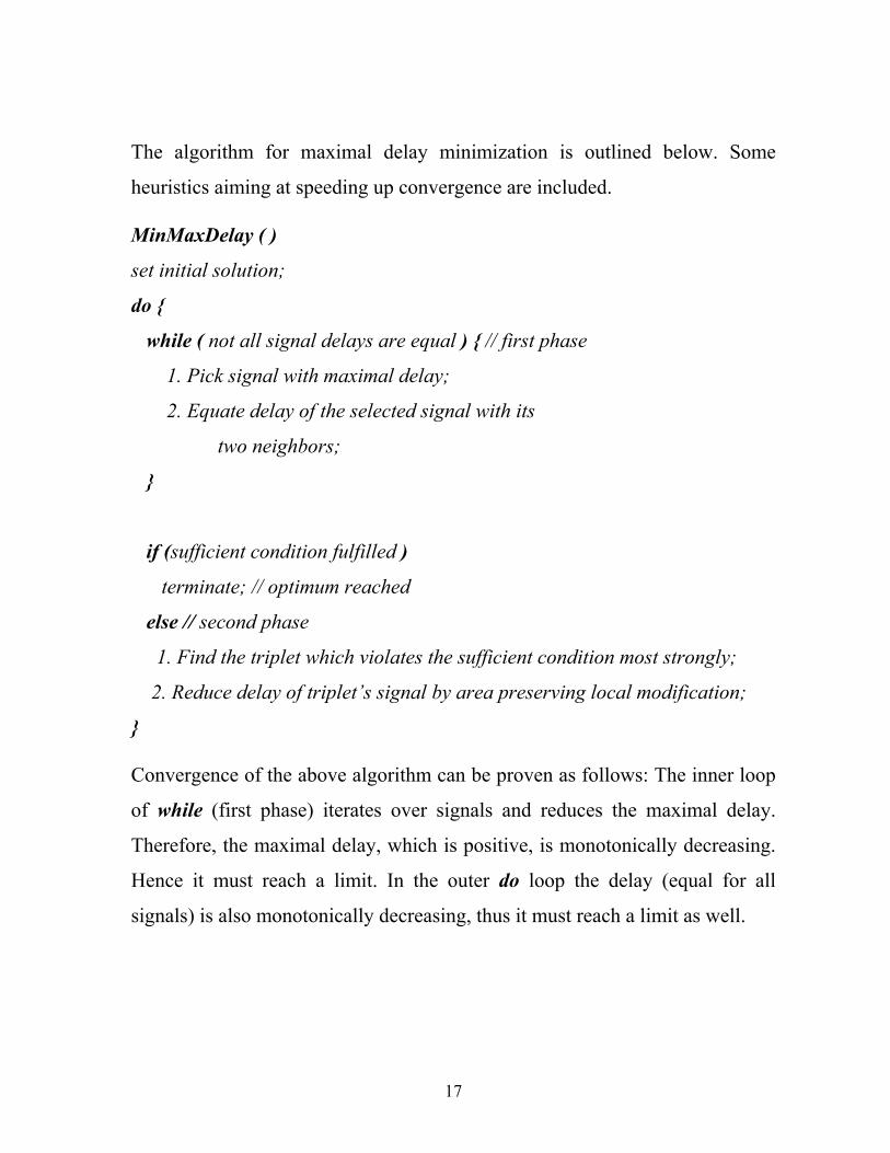
17
The algorithm for maximal delay minimization is outlined below. Some
heuristics aiming at speeding up convergence are included.
MinMaxDelay ( )
set initial solution;
do
while ( not all signal delays are equal ) // first phase
1. Pick signal with maximal delay;
2. Equate delay of the selected signal with its
two neighbors;
if (sufficient condition fulfilled )
terminate; // optimum reached
else // second phase
1. Find the triplet which violates the sufficient condition most strongly;
2. Reduce delay of triplet’s signal by area preserving local modification;
Convergence of the above algorithm can be proven as follows: The inner loop
of while (first phase) iterates over signals and reduces the maximal delay.
Therefore, the maximal delay, which is positive, is monotonically decreasing.
Hence it must reach a limit. In the outer do loop the delay (equal for all
signals) is also monotonically decreasing, thus it must reach a limit as well.

18
The relation between minimal total sum and MinMax solutions
We further study the relation between the optimal solutions of total sum and
MinMax optimizations, for either delay or slack optimizations. We may
interpret the delay (slack) of the bus ( )n∆∆≡∆ ,...,1 (analogously for slacks)
as a vector in n dimensional vector space over real positive numbers. The
addition of delay (slack) vectors is interpreted as connecting two busses
serially, signal by signal. It is not difficult to prove that the objective function
of total sum of slacks (10) or delays (11), and the objective function of max
slack (12) or delay (13) are nothing but the norms1 and
∞, respectively.
Let Vv∈ be any vector in n dimensional vector spaceV . The norm
equivalence theorem states that there exist real positive numbersα andβ
satisfying βα <<∞
vv1 . This means that an optimal solution of
minimizing the total sum of delays is also a good MinMax solution and vice
versa. Indeed, the following theorems claim that the optimal solution of the
MinMax problem is bounded from both sides by the optimal solution of the
total sum problem. The notation is shown in Figure 4, illustrating distributions
of signal delays in the solution of a minimal total delay problem and in the
solution of the corresponding MinMax delay problem.

19
Figure 4: Distributions of signal delays in MinMax solution (top) compared with minimal
sum-of-delays solution (bottom).
Theorem 3: Let∆′ , ~∆ and ∆ ′′ be the smallest, average and largest delay,
respectively, among all the bus signals in the optimal solution of minimal total
sum of delay. Let *∆ be the delay of each signal in the MinMax optimal
solution. There exists then ∆ ′′≤∆≤∆≤∆′ *~ .
Proof: The inequality ∆ ′′≤∆≤∆′ ~ is satisfied by definition. It is impossible
that ~* ∆<∆ . Otherwise, the optimal MinMax solution yields total sum of
delay *∆n , thus contradicting the optimality of ~∆n . It is also impossible that *∆<∆ ′′ as it yields a solution whose max delay is smaller than *∆ ,
contradicting the optimality of *∆ .

20
Theorem 4: LetΩ′ , ~Ω and Ω′′ be the smallest, average and largest slack of
a signal, respectively, in the optimal solution of maximal total sum of slack.
Let *Ω be the slack of a signal in the MinMax optimal solution. There exists
then Ω′′≤Ω≤Ω≤Ω′ *~ .
Examples
Exampel 1: Sidewall effects in a uniform bus.
Figures 5 and 6 illustrate the optimal solutions of MinMax and sum-of-delays
optimization, respectively. The bus has eight signals whose wire length is 500
microns. All drivers are of 500Ω resistance and all load capacitances are
50 fF . The area allocated for the bus is 7 microns.

21
Figure 5: ( Top): Cross section of the bus after MinMax delay optimization, annotated
with values of wire widths and spaces. (Bottom): Width and spaces shown as graphs versus
wire position in the bus.
0.0
0.1
0.2
0.3
0.4
0.5
0.6
0.7
1 2 3 4 5 6 7 8 9
Spac
es, u
m
0.2350.240.2450.250.2550.260.2650.270.2750.280.285
1 2 3 4 5 6 7 8
Wid
ths,
um
Spaces between wires Widths of wires
0.486 0.596 0.533 0.559 0.542 0.559 0.533 0.596 0.4860.279 0.250 0.266 0.261 0.261 0.266 0.250 0.279
67.562 67.562 67.562 67.562 67.562 67.562 67.562 67.562
Widths [um] Spaces [um]
Delays [ps]

22
Figure 6: ( Top): Cross section of the bus after sum-of-delays optimization, annotated with
values of wire widths and spaces. (Bottom): Width and spaces shown as graphs versus wire
position in the bus.
In case of MinMax optimization all signal delays are identical as expected.
Notice that wire width and space have ‘oscillations’ decaying towards the
center of the bus. This is caused by the side walls, which get relatively small
spaces to the extreme wires, because unlike all other spaces their cross-
capacitance is not shared by two signals. The narrow space needs
0
0.1
0.2
0.3
0.4
0.5
0.6
0.7
1 2 3 4 5 6 7 8 9
Spac
es, u
m
0.263
0.264
0.265
0.266
0.267
0.268
0.2691 2 3 4 5 6 7 8
Wid
ths,
um
Spaces between wires Widths of wires
0.409 0.579 0.579 0.579 0.579 0.579 0.579 0.579 0.4090.268 0.265 0.265 0.265 0.265 0.265 0.265 0.268
68.771 67.041 67.039 67.038 67.038 67.038 67.040 68.775
Widths [um] Spaces [um]
Delays [ps]

23
compensation by a wide wire, otherwise large RC delay will occur. This
phenomenon repeats itself for the next adjacent wires, with decreasing
amplitude. In the minimization of sum-of-delays, the first and last wires are
affected similarly as in MinMax optimization due to same reason: sidewalls
don’t care for space. All other signals however have the same width and space.
Consequently, the extreme wires have larger delay than all others. Despite
differences in width-space distributions between two cases, numerical values
of delays are very close. Comparing average delay obtained in sum-of-delays
optimization with delay obtained by MinMax optimization yield ~ 67.473 psec∆ = and * 67.562 psec∆ = , which are indeed very close.
For deeper insight while comparing total sum-of-delays with MinMax
problems, let’s simplify the bus model and ignore the sidewall effect. This is
done by dropping the sidewalls and assuming that the leftmost signal and the
rightmost signal are adjacent. Pictorially, it is equivalent to placing the signal
bus on a cylindrical surface, thus obtaining two neighbors for every signal.
The optimal solution satisfies the following theorem whose proof is given in
Appendix B.
Theorem 5: Let all signals have identical drivers and identical receivers and
let their order be cyclical (placed on a cylindrical surface). Then in the
optimal solution of maximizing (minimizing) the total sum of slacks (delays),
all the widths, spaces and delays are necessarily equal.
We now characterize the optimal solution of MinMax delay in a cyclical
uniform bus by a direct consequence of Theorems 3 and 5 above.

24
Corollary 1: For a cyclical bus where all signals have identical drivers and
identical receivers, the minimization of max delay yields the same solution as
the minimization of total sum of delays.
Proof: Follows directly from Theorem 3 which states
that ∆ ′′≤∆≤∆≤∆′ *~ , where ∆′ , ~∆ and ∆ ′′ are the smallest, average and
largest delays in the minimal total sum of delays, respectively, and *∆ is the
delay of a signal in the optimal MinMax solution. Theorem 5 states that for
cyclic uniform bus there exists ∆ ′′=∆=∆′ ~ . Hence the corollary follows.
Returning to Example 1 above, let us modify the bus to be cyclical. Both
MinMax optimization and minimal sum-of-delay optimization were solved in
MATLAB and yielded a result 65.524 psec . In conclusion, a uniform bus is
similar to a cyclical bus, except for the edge effects near the sidewalls.
Therefore, optimal solutions for total delay and MinMax delay are almost
identical. Note that the identity of optimal solutions for total sum and MinMax
doesn’t exist for slacks, even in a uniform cyclical bus. Maximizing total sum
of slacks is the same as minimizing total sum of delays; hence delays of
signals are all equal in the optimized uniform cyclical bus. Slacks, however,
are not equal to each other as they depend on the required time which may
change from signal to signal. In the optimal solution of the MinMax slack
problem, all slacks are equal.
The next example deals with optimizing total slack and worst slack in a
uniform bus with side walls.
25
Example 2: Slack optimization.
Figures 7 illustrates the case where a required time is assigned to each signal.
Using the same bus from example 1, a required time of 65 picoseconds was
assigned to the fifth wire, while all other wires were allowed 70 picoseconds.
Applying MinMax optimization of the slacks results in equal slacks of 1.4
picoseconds for all signals, as shown in Figure 7. The distribution of wire
widths and spaces is depicted in the bottom part of Figure 7. Its nature is
similar to the case of MinMax delay optimization. Notice however that the
non-uniformity in required time disturbs the symmetry obtained in Example 1.
The wire which was assigned the most difficult (earliest) required time became
wide, while its spacing to adjacent wires became larger too. This is for the
sake of reducing its RC delay, thus compensating for the early required time.
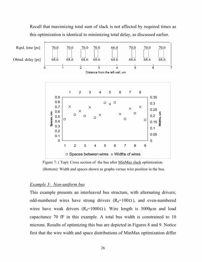
26
Recall that maximizing total sum of slack is not affected by required times as
this optimization is identical to minimizing total delay, as discussed earlier.
Figure 7: ( Top): Cross section of the bus after MinMax slack optimization.
(Bottom): Width and spaces shown as graphs versus wire position in the bus.
Example 3: Non-uniform bus
This example presents an interleaved bus structure, with alternating drivers;
odd-numbered wires have strong drivers (Rd=100Ω ), and even-numbered
wires have weak drivers (Rd=1000Ω ). Wire length is 3000µm and load
capacitance 70 fF in this example. A total bus width is constrained to 10
microns. Results of optimizing this bus are depicted in Figures 8 and 9. Notice
first that the wire width and space distributions of MinMax optimization differ
00.10.20.30.40.50.60.70.80.9
1 2 3 4 5 6 7 8 9
Spac
es, u
m
0
0.05
0.1
0.15
0.2
0.25
0.3
0.351 2 3 4 5 6 7 8
Wid
ths,
um
Spaces between wires Widths of wires
Rqrd. time [ps]
Obtnd. delay [ps]
66.070.0 70.0 70.0 70.0 70.0 70.0 70.0
68.6 68.6 68.6 68.6 68.6 68.6 68.664.6

27
significantly from total sum-of-delays minimization. Since in MinMax
optimization all the delays must be equal, and since the weak and strong
drivers are interleaved, the spaces must be equal to each other. An exception is
the leftmost space. This is due to the asymmetry resulting from a strong driver
on the left side and a weak driver on the right side of the bus. The equality of
spaces and signal delays implies that signals with strong drivers will be
narrower than those driven by weak drivers, as demonstrated in the bus cross
section. Minimization of total sum-of-delay also yields alternating widths of
wires, but neither uniformity nor symmetry exists. Notice also that wider wires
were allocated to strong drivers in this case. It is interesting to compare the
delays obtained by the two optimizations. Although all the relations proved in
Theorem 3 do exist, the MinMax delay is much worse than the average delay
in the total sum-of-delay optimization. In fact, it is very close to the maximal
delay of the latter distribution.

28
Figure 8: Non uniform bus minmax optimization
Example 5: Optimal delay dependency on bus width.
Let us change the total width of the bus in example 4. The MinMax delay is
compared to the minimum, average and maximum delay of the corresponding
total sum-of-delays optimization, for various bus widths, as illustrated in
Figure 9. According to Theorem 3, the MinMax delay of all wires always
resides between the average and the maximal wire delay in the total sum-of-
delay minimization. As the bus width constraint is relaxed (larger widths), the
MinMax result approaches the maximal delay of the other optimization. This
0
0.2
0.4
0.6
0.8
1
1.2
1 2 3 4 5 6 7 8 9
Spac
es, u
m
00.050.10.150.20.250.30.35
1 2 3 4 5 6 7 8
Wid
ths,
um
Spaces between wires Widhts of wires
0.118 1.029 1.029 1.029 1.029 1.029 1.029 1.032 1.026
0.199 0.287 0.101 0.287 0.101 0.287 0.101 0.287
486.733 486.733 486.733 486.733 486.733 486.733 486.733 486.733
Widths [um]
Spaces [um]
Delays [ps]

29
is due to the fact that large bus width decouples the signals, so signals of weak
and strong drivers are optimized independently.
Figure 9: Non uniform bus total sum of delays optimization
00.10.20.30.40.50.60.70.80.9
1
1 2 3 4 5 6 7 8 9
Spac
es, u
m
0
0.1
0.2
0.3
0.4
0.5
0.6
0.71 2 3 4 5 6 7 8
Wid
ths,
um
Spaces between wires Widhts of wires
0.328 0.850 0.671 0.673 0.786 0.773 0.930 0.733 0.854
0.595 0.283 0.515 0.285 0.590 0.288 0.558 0.290
212.270 515.745 207.916 519.150 196.426 503.564 197.807 509.981
Widths [um]
Spaces [um]
Delays [ps]

30
Figure 10: Optimal solution parameters ∆ ′′∆∆∆ ′ ,,, *~ (see Figure 4) versus bus width
constraint A, for the circuit of example 4.
Example 6. Migration of a bus in an industrial circuit.
A 20-wire metal 3 bus structure from an industrial circuit block was migrated
from 90 nanometer to 65 nanometer technology, with a clock frequency target
of several GHz. The total width of the bus is 13.53 µm, length of wires is 500
µm. Before optimization, wire widths and spaces were determined by
shrinking the old layout, as specified in Table I below. Two kinds of drivers
are used in the bus: strong drivers with resistance of 85 Ω and input
capacitance of 14 fF and weak drivers with resistance of 2.17 KΩ and input
capacitance of 0.75 fF.
020406080
100120140160180200
2 4 6 8 10 12 14 16 18 20
Bus width (A), um
Del
ay, p
s
Delay after MinMaxopt.Avrg. delay aftertotal sum opt.Min delay of wire intotal sum opt.Max delay of wire intotal sum opt.

31
Table I: Migration of a circuit block in 65 nanometer technology
Before optimization After optimization
Wire
no.(i)
driverR
[ KΩ ]
loadC
[fF] 1iS −
[µm]
iW
[µm]
Delay
(% of clock
cycle time)
1iS −
[µm]
iW
[µm]
Delay
(% of clock
cycle time)
1 2.17 0.75 0.33 0.33 46.5 0.54 0.11 34.9
2 2.17 0.75 0.33 0.33 44.5 0.86 0.11 33.2
3 0.085 14 0.33 0.33 6.4 0.46 0.11 14.3
4 2.17 0.75 0.33 0.33 44.8 0.65 0.11 32.9
5 0.085 14 0.33 0.33 6.4 0.72 0.11 10.8
6 2.17 0.75 0.33 0.33 45.2 0.29 0.11 38.3
7 0.085 14 0.33 0.33 6.4 0.26 0.16 10.3
8 2.17 0.75 0.33 0.33 44.0 0.34 0.11 36.0
9 2.17 0.75 0.33 0.33 44.2 0.31 0.11 34.4
10 2.17 0.75 0.33 0.33 43.8 0.7 0.11 32.6
11 0.085 14 0.33 0.33 6.6 0.47 0.14 13.0
12 0.085 14 0.33 0.33 6.2 0.21 0.11 14.8
13 2.17 0.75 0.33 0.33 44.1 0.9 0.11 32.4
14 2.17 0.75 0.33 0.33 44.1 0.58 0.11 33.4
15 0.085 14 0.33 0.33 6.6 0.42 0.11 14.6
16 2.17 0.75 0.33 0.33 44.6 0.42 0.11 33.4
17 0.085 14 0.33 0.33 6.6 0.93 0.16 9.7
18 2.17 0.75 0.33 0.33 45.2 0.52 0.11 34.2
19 0.085 14 0.33 0.33 6.6 0.5 0.11 14.7
20 2.17 0.75 0.33 0.33 44.6 0.57 0.11 33.4
Average 29.4 25.6
Total sum of delays timing optimization was run on this bus and results are
presented in Table I. The delays in Table I were obtained from circuit
32
simulations, performed with extracted parasitics from actual layouts before
and after optimization, using accurate industrial tools. The delays are
represented as a percentage of the clock cycle time. As seen in the table,
average timing of the bus was improved by about 13%. It was achieved by
decreasing widths of wires and varying spaces, thus decreasing wire
capacitances on the slower signals. As expected, the timing improvement of
critical signals as well as the improvement in total sum of delays were
obtained by trading off the less critical signals whose delay got worse. Almost
all wires were narrowed to the minimal allowed value of 0.11 µm. Since the
bus is relatively short, wire resistance effect is not critical and therefore most
of the channel area was allocated to inter wire spaces in order to decrease
loading of weak drivers by inter-wire cross capacitances. Minimization of
worst wire delay has also been performed, and results were verified by circuit
simulation, using extracted layout capacitances and resistances, yielding
36.2% of clock cycle time versus 46.5% before optimization (compare with
the average wire delay of 25.6% and maximum wire delay of 38.3% in sum of
delays optimization). Elmore delay estimates were about 35% larger than
circuit simulation results.
Discussion and conclusions
It has been noted in general circuit timing optimization that whenever
MinMax formulation is used, all timing paths tend to become equally critical,
as proven in theorem 1 for the bus sizing problem. This phenomenon was
termed path-balancing [ 17][ 18]. Shaping of delay distributions involves a
number of considerations: minimization of critical delay for maximal circuit
speed tends to push the right tail of the path delay distribution towards the
center, and minimization of area and power often tends to push the left tail

33
towards the center. Circuit tuning by MinMax optimization results in a very
narrow distribution of delays, as illustrated in figure 4. However, a narrow
distribution where many paths are critical, is more sensitive to parameter
variability [ 17, 18, 19]. A modification of the objective function in MinMax
formulation has been proposed, involving a penalty function [ 18] which
separates the most critical paths from others. An alternative approach is to use
the total sum objective, at least in the initial stages of layout migration. At the
optimal the solution of total sum minimization, every wire is at a balance point
where sensitivity to the value of wire width and spaces approaches zero, as
illustrated in Figure 3. In contrast, the MinMax solution takes most signals
away from this stable point in order to equalize all of the delays or slacks, and
therefore the circuit becomes more sensitive to variations in geometrical
dimensions. Our computational experiments in bus tuning show that typically,
most signal delays become much worse while the critical signal become only
slightly better as resources are shifted to make all wires equally critical. In
other words, the largest wire delay in the total sum solution is typically a tight
bound on the solution of the MinMax problem, as seen in the example of
Figure 9.
In conclusion, we have characterized the problem of simultaneously allocating
wire widths and spaces to all wires in parallel bus structures under a total area
constraint, for circuit performance optimization. We have demonstrated its
importance in migration of layouts to new generations of CMOS process
technology. Our results show that total sum of delays (or slacks) is a useful
objective function for minimization. Compared with MinMax delay tuning, it
is mathematically more convenient, leads to robust solutions which are less
sensitive to parameter variations, and typically produces bus layouts which

34
closely approach the best achievable performance. We have also presented an
iterative algorithm for MinMax performance tuning of bus layouts, based on
problem-specific necessary and sufficient conditions for optimality.
Appendix A: The optimization problems are all convex
Proposition: The objectives functions 4321 ,,, ffff presented above are all
convex or concave. Their associated constraints are linear, and therefore also
convex. Consequently all the optimization problems have unique, global
minimum or maximum, depending on convexity or concavity.
Proof: The area and design rules constraints given in (3), (4) and (5) are all
linear equalities or inequalities. Altogether they define a convex feasible
region on which the above objective functions are defined.
The function ( )SWi ,∆ in (2) is a sum of terms depending on the
variables iW , iS and 1−iS . In order to prove its convexity it is sufficient to see
the convexity for each term, since a linear combination with positive
coefficients of convex functions is convex too. Convexity exists if all its
second order derivatives are non-negative. Deriving twice all the terms
comprising ∆ yields 02 =∂∂
WW ; 021
32 >=∂∂
WWW
; 02132 >=
∂∂
SWWWS ;
011122 >=
∂∂∂
=∂∂
∂SWWS
WSSW
WS ; 02132 >=
∂∂
WSSWS , which are all nonnegative.
Consequently, the delay of single signal is convex

35
The function 1f defined in (10) is a negative sum of convex terms and
therefore yields a concave function. Its maximization on convex region yields
unique global maximum. For similar reasons, 2f defined in (11) is convex
and has therefore global minimum.
Both functions 3f and 4f of maximal slack delay as defined in (12) and (13),
respectively, are convex since they are a maximum of convex functions. Their
minimization on convex region yields therefore a unique global minimum.
Appendix B: Proof of Theorem 5
Proof: From (11) we obtain:
(23)
++
+++++= ∑∑∑∑
= −=== 112 11112
111111121SSWSSW
eS
dW
cnbWafn
n
i iii
n
i i
n
i i
n
ii .
In the above we identify 0S with nS due to the cyclic ordering of signals. Note
also that the coefficients are not indexed since all drivers and receivers are
identical.
Assume that the optimization problem (3), (18) and (19) was solved and the
optimal solution is given. Let ∑ ==
n
j jWW1 and ∑ =
=n
j jSS1 denote the total
wire widths and total spacing in the optimal solution. Obviously, there
exists SWA += . Let us show that among all the settings of area preserving
W and s , the one in which all iW and is are identical is optimal.
36
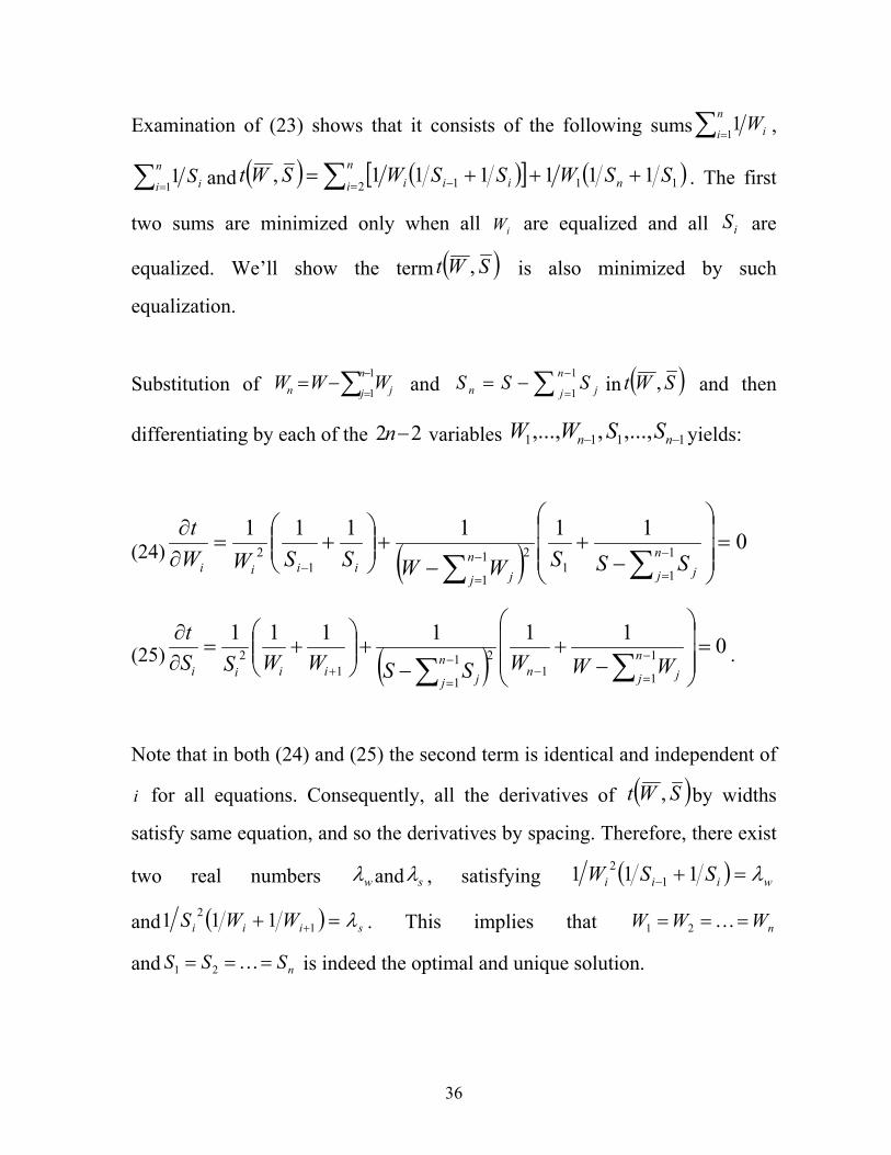
Examination of (23) shows that it consists of the following sums∑=
n
i iW11 ,
∑=
n
i iS11 and ( ) ( )[ ] ( )112 1 111111, SSWSSWSWt n
n
i iii +++= ∑ = − . The first
two sums are minimized only when all iW are equalized and all iS are
equalized. We’ll show the term ( )SWt , is also minimized by such
equalization.
Substitution of ∑−
=−=
1
1
n
j jn WWW and ∑ −
=−=
1
1
n
j jn SSS in ( )SWt , and then
differentiating by each of the 22 −n variables 1111 ,...,,,..., −− nn SSWW yields:
(24) ( ) 01111111
1121
11
2 =
−+
−+
+=
∂∂
∑∑−
=−
=−
n
j jn
j jiiii SSSWWSSWW
t
(25) ( ) 01111111
1121
11
2 =
−+
−+
+=
∂∂
∑∑−
=−−
=+
n
j jnn
j jiiii WWWSSWWSSt
.
Note that in both (24) and (25) the second term is identical and independent of
i for all equations. Consequently, all the derivatives of ( )SWt , by widths
satisfy same equation, and so the derivatives by spacing. Therefore, there exist
two real numbers wλ and sλ , satisfying ( ) wiii SSW λ=+− 111 12
and ( ) siii WWS λ=+ +12 111 . This implies that nWWW === …21
and nSSS === …21 is indeed the optimal and unique solution.

37
In conclusion, minimal total sum of delays requires identical wire widths and
identical wire spacing. Identical signal delays follow immediately due to
identical drivers and identical receivers.
Appendix C: Proof of Theorem 2
Proof: Assume to the contrary that a given equal delay solution is not
minimal. According to the above postulate there exists area preserving local
modifications that will reduce the delay of a signal without increasing the
delay of any other signal. Four modifications are possible: Increasing or
decreasing wire width, and increasing or decreasing a space. Let us consider
each.
Case 1: Increasing wire width is impossible since area preservation implies
that at least one of the adjacent spaces is decreased. This however increases
the delay of the adjacent signal that shares this space.
Case 2: Decreasing the width results in the new
triplet ( )( )εαεαε −+−+− 1,,1 iii SWS , where 10 ≤≤ α . The delays 1−∆i and
1+∆i do not increase as their adjacent spaces do decrease. For the new delay
i∆′ to decrease there must exist some 10 ≤≤ α , such that substitution of the
new width and spaces in (2) yields
( )2
1222
12
1110 εααε OSSW
eSSW
edWca
iiiiiii
i
iiii +
+−
−+
++−=∆′−∆≤
−−

38
Dropping the term ( )2εO implies that delay reduction requires the above
square brackets to be positive. Case 1 can be viewed as being obtained by
using negativeε , thus implying an opposite inequality than the above. Hence
equation (20) follows.
Case 3: Decreasing a space results in the new
triplet ( )( )εαεαε −+−+ + 1,, 1iii WSW . We require that none of i∆ and 1+∆i is
increased. This implies the for some 10 ≤≤α , there exists
( )22
122
1110 εαε OSW
edSSW
eWca
iii
iiii
iiii +
+−
+++−=∆′−∆≤
−
( ) ( )22
11
12
12
1111
11110 εαε OSW
edSSW
eW
ca
iii
iiii
iiii +
+−
+++−−=∆′−∆≤
++
++++++
Dropping the term ( )2εO implies that delay reduction requires the above
square brackets to be positive. Hence (21) and (22) must be non negative.
Case 4: Increasing a space results in the new
triplet ( )( )εαεαε −−+− + 1,, 1iii WSW . This is exactly the same as case 3, but
with negativeε . Therefore, the braces need now be non positive.

39
Acknowledgment The authors are thankful to the anonymous reviewers for their valuable comments that helped to improve this manuscript.
References
1. R. Ho, K. Mai and M. Horowitz, “The future of wires”, Proceedings of the IEEE, Vol. 89, no. 4, Apr. 2001.
2. D. Sylvester and K. Keutzer, “Getting to the bottom of deep submicron”, in Proc. ICCAD, pp. 203-211, 1998.
3. Kahng, S. Muddu, E. Sarto and R. Sharma, "Interconnect Tuning Strategies for High-Performance ICs", Proc. Design, Automation and Testing in Europe, Paris, February 1998.
4. J. Cong and K. S. Leung, "Optimal Wiresizing Under Elmore Delay Model". IEEE Trans. on Computer-Aided
Design, vol. 14, no. 3, pp. 321-336, Mar. 1995.
5. S. S. Sapatnekar, "Wire Sizing as a Convex Optimization Problem: Exploring the Area Delay Tradeoff", IEEE Transactions on Computer-Aided Design of Integrated Circuits and Systems, Vol. 15, No. 8, pp. 1001 - 1011, August 1996.
6. C. Chu and D. F. Wong, “Closed Form Solution to Simultaneous Buffer Insertion / Sizing and Wire Sizing”,
ACM Transactions on Design Automation of Electronic Systems, vol. 6, no. 3, pages 343-371, July 2001.
7. C.P. Chen, C. N. Chu and D. F. Wong, “Fast and exact simultaneous gate and wire sizing by Lagrangian relaxation”, in Proc. ICCAD , pp. 617-624, 1998.
8. J. Cong, L. He, C. K. Koh and Z. Pan, "Interconnect Sizing and Spacing with Consideration of Coupling
Capacitance", IEEE Transactions on Computer-Aided Design of Integrated Circuits and Systems, vol. 20, no. 9, pp.1164-1169, September 2001.
9. J. Lillis, C. K. Cheng, and T. T. Y. Lin, “Simultaneous routing and buffer insertion for high performance
interconnect,” in Proc. 6th Great Lakes Symp. VLSI, Mar. 1996, pp. 148–153.
10. M. Becer, D. Blaauw, V. Zolotov, R. Panda, I. Hajj, “Analysis of Noise Avoidance Techniques in Deep-Submicron Interconnects Using a Complete Crosstalk Noise Model”, IEEE/ACM Design Automation and Test in Europe Conference (DATE), March 2002, pp. 456-463.
11. D. A. Kirkpatrick and A. L. Sangiovanni-Vincentelli. “Techniques for crosstalk avoidance in the physical
design of high performance digital systems”, In Proc. IEEE/ACM Int. Conf. Computer Aided Design, pp. 616--619, Nov. 1994.
12. R. Arunachalam, E. Acar, and S. R. Nassif, “Optimal shielding/spacing metrics for low power design”,
Proceedings of IEEE Computer Society Annual Symposium on VLSI, pp. 167-172, 2003.
13. J. Cong, D. Z. Pan and P. V. Srinivas, "Improved Crosstalk Modeling for Noise Constrained interconnect Optimization", ACM/IEEE International Workshop on Timing Issues in the Specification and Synthesis of Digital Systems, pp. 14-20, Austin, December 2000.
14. S. Wong, G. Lee, and D. Ma, “Modeling of Interconnect Capacitance, Delay, and Crosstalk in VLSI”, IEEE
Transactions on Semiconductor Manufacturing, vol. 13, No. 1, pp. 108-111, Feb. 2000.
15. A. Abou-Seido, B. Nowak and C. Chu, “ Fitted Elmore Delay: A Simple and Accurate Interconnect Delay Model”, IEEE Transactions on VLSI Systems, vol. 12, no. 7, pages 691-696, July 2004.
16. P. Chen, D. A. Kirkpatrick and K. Keutzer, “Miller Factor for Gate-Level Coupling Delay Calculation”, in
Proc. ICCAD, pp.68-74, 2000.

40
17. M. Hashimoto and H. Onodera, ”Increase in delay uncertainty by performance optimization”, Proc. IEEE International Symposium on Circuits and Systems (ISCAS), pages 379--382, 2001.
18. X. Bai, C. Visweswariah, P. N. Strenski, D. J. Hathaway, "Uncertainty-Aware Circuit Optimization”, The 39th Design Automation Conference (DAC), 2002, pp.58~63.
19. S. Borkar, T. Karnik, S. Narendra, J. Tschanz, A. Keshavarzi and V. De: ” Parameter variations and impact on
circuits and microarchitecture”, Design Automation Conference (DAC) 2003, pp. 338-342.