
Optically assisted Internet routing using arrays of novel dynamically reconfigurable FBG-based...
14
JOURNAL OF LIGHTWAVE TECHNOLOGY, VOL. 21, NO. 11, NOVEMBER 2003 2765 Optically Assisted Internet Routing Using Arrays of Novel Dynamically Reconfigurable FBG-Based Correlators Michelle C. Hauer, Student Member, IEEE, Student Member, OSA, John E. McGeehan, Student Member, IEEE, Saurabh Kumar, Student Member, IEEE, Joseph D. Touch, Senior Member, IEEE, Joseph Bannister, Senior Member, IEEE, Edward R. Lyons, Member, IEEE, C. H. Lin, A. A. Au, H. P. Lee, Member, IEEE, Dmitry S. Starodubov, Member, IEEE, and Alan Eli Willner, Fellow, IEEE, Fellow, OSA Abstract—As routing tables in core Internet routers grow to ex- ceed 100 000 entries, it is becoming essential to develop methods to reduce the lookup time required to forward packets toward their destinations. In this paper, we employ a bank of novel thermally tuned fiber-Bragg-grating-based optical correlators to construct an “optical bypass” to accelerate conventional electronic Internet routers. The correlators are configured as a routing table cache that can quickly determine the destination port for a fraction of the incoming traffic by examining only a subset of the bits in an IP packet’s 32-bit destination address.We also demonstrate a novel multiwavelength correlator based on fiber Bragg grating that can simultaneously recognize the header bits on multiple wavelengths for use in wavelength-division-multiplexed (WDM) systems. Using the optical bypass, routing table lookup times are reduced by an order of magnitude from microseconds to nanoseconds and are limited only by the speed of the optical switch. Index Terms—Optical communications, optical correlators, op- tical signal processing, wavelength-division-multiplexed (WDM) networks. I. INTRODUCTION I N present-day fiber-optic networks, data packets are con- verted to electrical form at each node to process their headers and make routing decisions, as shown in Fig. 1(a). As routing tables grow in size, more memory accesses are required to deter- mine the next-hop address and appropriate output port to which to forward each packet. The associated increase in routing-table lookup times is becoming a significant source of latency in the network core. To make matters worse, the transmission capacity of optical fibers is rapidly increasing, forcing the routers to ac- commodate more packets, more often. Since routing tables will Manuscript received December 20, 2002; revised May 22, 2003. This work was supported in part by Intel and in part by the NSF Optical Networks initiative. M. C. Hauer, J. E. McGeehan, S. Kumar, and A. E. Willner are with the Department of Electrical Engineering—Systems, University of Southern Cal- ifornia, Los Angeles, CA 90089-2565 USA (e-mail: [email protected]). J. D. Touch and J. Bannister are with the Information Sciences Institute, Uni- versity of Southern California, Marina del Rey, CA 90292-6695 USA (e-mail: [email protected]). E. R. Lyons is with Raytheon, El Segundo, CA 90245 USA (e-mail: [email protected]). C. H. Lin, A. A. Au, and H. P. Lee are with the Department of Electrical and Computer Engineering, University of California Irvine, Irvine, CA 92697 USA (e-mail: [email protected]). D. S. Starodubov is with Sabeus Photonics, Chatsworth, CA 91311 USA (e-mail: [email protected]). Digital Object Identifier 10.1109/JLT.2003.819144 (a) (b) Fig. 1. (a) Electronic Internet router architecture. Incoming optical packets are converted to electrical form and stored in a buffer while their 32-bit addresses are compared to a large routing table to determine to which output ports to forward them. The packets are electronically switched and converted back to optical form for transmission. (b) Longest prefix match example using an 8-bit address. continue to grow and transmission rates are always on the rise, it is essential to develop methods to reduce the lookup time re- quired to forward incoming IP packets. This motivates the need for optical designers to examine the operations of current elec- tronic routers to determine where it may be feasible to employ optical techniques to assist the electronics in making ultrafast routing decisions. IP routers perform two primary functions: routing and for- warding. Routing is the process of generating the lookup table of destination addresses and corresponding next-hop addresses and output ports. Routing tables in the network core are fairly stable and are typically recomputed on a timescale of tens of minutes to reflect the continually evolving layout of the net- work. Forwarding is the process of steering packets toward their 0733-8724/03$17.00 © 2003 IEEE
-
Upload
independent -
Category
Documents
-
view
1 -
download
0
Transcript of Optically assisted Internet routing using arrays of novel dynamically reconfigurable FBG-based...

JOURNAL OF LIGHTWAVE TECHNOLOGY, VOL. 21, NO. 11, NOVEMBER 2003 2765
Optically Assisted Internet Routing UsingArrays of Novel Dynamically Reconfigurable
FBG-Based CorrelatorsMichelle C. Hauer, Student Member, IEEE, Student Member, OSA, John E. McGeehan, Student Member, IEEE,
Saurabh Kumar, Student Member, IEEE, Joseph D. Touch, Senior Member, IEEE,Joseph Bannister, Senior Member, IEEE, Edward R. Lyons, Member, IEEE, C. H. Lin, A. A. Au,
H. P. Lee, Member, IEEE, Dmitry S. Starodubov, Member, IEEE, and Alan Eli Willner, Fellow, IEEE, Fellow, OSA
Abstract—As routing tables in core Internet routers grow to ex-ceed 100 000 entries, it is becoming essential to develop methods toreduce the lookup time required to forward packets toward theirdestinations. In this paper, we employ a bank of novel thermallytuned fiber-Bragg-grating-based optical correlators to constructan “optical bypass” to accelerate conventional electronic Internetrouters. The correlators are configured as a routing table cachethat can quickly determine the destination port for a fraction ofthe incoming traffic by examining only a subset of the bits in an IPpacket’s 32-bit destination address.We also demonstrate a novelmultiwavelength correlator based on fiber Bragg grating that cansimultaneously recognize the header bits on multiple wavelengthsfor use in wavelength-division-multiplexed (WDM) systems. Usingthe optical bypass, routing table lookup times are reduced by anorder of magnitude from microseconds to nanoseconds and arelimited only by the speed of the optical switch.
Index Terms—Optical communications, optical correlators, op-tical signal processing, wavelength-division-multiplexed (WDM)networks.
I. INTRODUCTION
I N present-day fiber-optic networks, data packets are con-verted to electrical form at each node to process their headers
and make routing decisions, as shown in Fig. 1(a). As routingtables grow in size, more memory accesses are required to deter-mine the next-hop address and appropriate output port to whichto forward each packet. The associated increase in routing-tablelookup times is becoming a significant source of latency in thenetwork core. To make matters worse, the transmission capacityof optical fibers is rapidly increasing, forcing the routers to ac-commodate more packets, more often. Since routing tables will
Manuscript received December 20, 2002; revised May 22, 2003. This workwas supported in part by Intel and in part by the NSF Optical Networks initiative.
M. C. Hauer, J. E. McGeehan, S. Kumar, and A. E. Willner are with theDepartment of Electrical Engineering—Systems, University of Southern Cal-ifornia, Los Angeles, CA 90089-2565 USA (e-mail: [email protected]).
J. D. Touch and J. Bannister are with the Information Sciences Institute, Uni-versity of Southern California, Marina del Rey, CA 90292-6695 USA (e-mail:[email protected]).
E. R. Lyons is with Raytheon, El Segundo, CA 90245 USA (e-mail:[email protected]).
C. H. Lin, A. A. Au, and H. P. Lee are with the Department of Electrical andComputer Engineering, University of California Irvine, Irvine, CA 92697 USA(e-mail: [email protected]).
D. S. Starodubov is with Sabeus Photonics, Chatsworth, CA 91311 USA(e-mail: [email protected]).
Digital Object Identifier 10.1109/JLT.2003.819144
(a)
(b)
Fig. 1. (a) Electronic Internet router architecture. Incoming optical packets areconverted to electrical form and stored in a buffer while their 32-bit addressesare compared to a large routing table to determine to which output ports toforward them. The packets are electronically switched and converted back tooptical form for transmission. (b) Longest prefix match example using an 8-bitaddress.
continue to grow and transmission rates are always on the rise,it is essential to develop methods to reduce the lookup time re-quired to forward incoming IP packets. This motivates the needfor optical designers to examine the operations of current elec-tronic routers to determine where it may be feasible to employoptical techniques to assist the electronics in making ultrafastrouting decisions.
IP routers perform two primary functions: routing and for-warding.Routingis the process of generating the lookup tableof destination addresses and corresponding next-hop addressesand output ports. Routing tables in the network core are fairlystable and are typically recomputed on a timescale of tens ofminutes to reflect the continually evolving layout of the net-work.Forwardingis the process of steering packets toward their
0733-8724/03$17.00 © 2003 IEEE

2766 JOURNAL OF LIGHTWAVE TECHNOLOGY, VOL. 21, NO. 11, NOVEMBER 2003
destinations by comparing their 32-bit destination addresses toentries in a routing table using a longest prefix matching algo-rithm. Thus, routing is analogous to drawing a map and for-warding is the act of following its directions. The basic con-cept of forwarding is illustrated in Fig. 1(b) for a packet with asimple 8-bit destination address of “11 010 100.” This addressis compared to entries in the routing table, where two matchesare found. The matching entry with the longest prefix is chosenand directs the packet to output port 3.
The forwarding process can be time consuming given thatcore routing tables have grown to contain more than 100 000entries. Lookup times are presently on the order of microsec-onds. Given that a significant portion of Internet packetsentering routers are short, 40-byte TCP/IP acknowledgementpackets, nanosecond lookup times are needed to achieve thedesired terabit/second throughput. Some efforts are beingmade to improve electronic hardware architectures and searchalgorithms to reduce lookup times [1], but the ideal case wouldbe for the packet headers to be processed on-the-fly usingoptical signal-processing techniques, so that the only limitationto throughput is the speed of the optical switch (currently afew nanoseconds). A true all-optical router would thereforeneed to be capable of 24-bit lookups into 100 000-entry ta-bles at Gb/s (since only 24 of the 32 address bits aregenerally significant for packet-forwarding in the networkcore). Unfortunately, such capabilities are beyond currentoptical technologies, which are limited to optical correlationtechniques. These techniques inherently suffer from highoptical splitting losses that limit them to matching incomingpackets against a few patterns that are a few bits long. However,some recent developments hint at the feasibility of a partialsolution in which presently achievable optical correlators maybe combined with a novel routing-table optimization algorithmto reduce lookup times by at least an order of magnitude frommicroseconds to nanoseconds.
Given that most core routers have only four to eight outgoingports, it may be possible to determine a packet’s output portby looking at only a small subset of the 24 bits in the desti-nation address. So although building a true all-optical router isbeyond current optical technologies, it is feasible to build an“optical bypass” to accelerate a conventional router. A subsetof the traffic would be routed by the optical bypass without anyO/E conversion, at increased throughput and decreased latency.The remainder of the traffic, which requires more complicatedprocessing, is handled by a conventional electronic router. Pre-vious research has shown that by utilizing a subset of the routingtable with as few as 100 of the most popular entries, the routercan still successfully forward as much as 90% of the incomingtraffic [2]. The remaining challenge is to determine how to de-sign a 24-bit input, 100-entry optical index using a manageablenumber of optical correlators that interrogate only a small subsetof the bits in the destination address.
The optical correlators required for this application mustbe tunable and designed to easily scale to 40 Gb/s and be-yond. Optical correlators are typically implemented withtapped-delay-line structures that split the optical signal intoseveral branches, where each successive branch delays thesignal 1 bit-time longer than the previous branch. The tiny
distances required to achieve these differential 1-bit delays infiber at bit rates Gb/s present a serious challenge forpreviously reported correlator designs. These designs includeoptical splitters followed by fiber delay lines terminated withfiber mirrors [3] and arrays of discrete fiber Bragg gratings(FBGs) tuned with separate piezoelectric stretchers [4]. Forthese cases, the intermirror or intergrating spacings would haveto be 2.5 mm for a 1-bit round-trip time delay at 40 Gb/s—animpractical length for devices using discrete fiber components.
In this paper, we propose and experimentally demonstrate acorrelator design in which an FBG array is constructed froma single uniform fiber grating that is divided into separate,electrically tunable sections using thin-film microheaters. Theprecision of the heater deposition defines the spacing betweengratings. Since thin-film heaters can be fabricated with litho-graphic precision, spacings down to hundreds of micrometersare achievable with this technology, enabling the correlator toreadily scale to higher bit rates.
An additional advance over previously reported correlator ar-chitectures is that our approach uses two grating arrays per cor-relator: one to correlate with the desired “1” bits in the inputsignal and another to match with the desired “0” bits. We showthat the combined outputs from both of these correlators are nec-essary to produce unique correlation outputs for all 2possible
-bit sequences.In wavelength-division-multiplexed (WDM) systems,
packets arrive at routing nodes on multiple wavelengths.For this case, a separate bank of correlators is required foreach incoming wavelength channel. To reduce the number ofcomponents required in a WDM routing node, we demonstratea correlator design that is constructed with sampled FBGsthat enables the headers on multiple wavelengths to be simul-taneously tested against a stored bit pattern. The correlationoperation can therefore be performed prior to demultiplexingand switching. This eliminates the need for multiple sets ofcorrelators and significantly reduces the required number ofcomponents in a WDM routing node.
This paper is structured as follows. In Section II, the conceptof an optically assisted Internet router is described along withthe constraints for the algorithm needed to define and configurethe optical routing table. Section III provides an overviewof digital optical correlation. Section IV presents a novelFBG-based correlator design and includes an experimentaldemonstration in which the correlators are used to process andswitch 10-Gb/s optical packets. In Section V, a multiwavelengthFBG-based optical correlator is described and demonstratedin a WDM system. Section VI includes a discussion of im-portant fabrication and performance considerations associatedwith using FBG arrays for optical correlation. This paper issummarized in Section VII.
II. OPTICALLY ASSISTEDINTERNET ROUTER
To implement an effective optical bypass for an electronicrouter, the key design decision is to combine a software algo-rithm with a small set of dynamically configurable FBG-basedoptical correlators. A conceptual diagram showing how the op-tical bypass is implemented in an IP router is shown in Fig. 2(a).

HAUER et al.: OPTICALLY ASSISTED INTERNET ROUTING USING FBG-BASED CORRELATORS 2767
(a)
(b)
Fig. 2. (a) Conceptual diagram of an Internet core router withN outputports (typically two to four) assisted by a bank ofM optical FBG-basedcorrelators that are dynamically configured by a software algorithm. (b) Thealgorithm searches the port can be determined by examining only a subsetK,of the n bits in the destination address. The correlators are then configuredcorresponding to these groups of entries. If all the correlators fail to match theincoming packet address, then the packet is switched to an auxiliary port andprocessed by conventional electronics.
A small portion of the incoming optical packet stream is tappedoff and sent to the correlator module. The optical signal is am-plified, split, and sent to correlators, each of which can beconfigured to produce a “match” signal for any numberofthe 24 significant bits in the destination address.
Previously, we reported on an algorithm for generating arouting table cache containing as few as 100 entries that couldsuccessfully route as much as 90% of the traffic entering anIP router [2]. Since a 100-entry lookup table is still too largeimplement optically, the goal here is to define an algorithmto represent this 100-entry table with as few as eight or tenoptical correlators. The fact that Internet routers typically haveonly two to four outgoing ports makes this feasible. Even ifthere are 100 000 entries, each of them only points to one oftwo or four possible destinations. The algorithm searches forpatterns among these entries for which the output port can bedetermined by examining only a subsetof the bits in thedestination address, with ideally less than five. An additional
goal of the software is to determine the optimum groupingsof these entries so as to minimize the numberof opticalcorrelators required. The software then configures each opticalcorrelator to represent one of the resulting groups.
This process is illustrated in Fig. 2(b). Note that there willlikely be multiple correlators corresponding to each output portsince there will be groups of bit patterns that the algorithm de-termines should all be routed to a particular port. For example,it is feasible that two correlators, each of which are configuredto match a different subset of address bits, both route packetsto the same port when they get a match. The algorithm must re-compute the optical lookup table and reconfigure the correlatorseach time the routing table is updated. Threshold detectors areused at the outputs of the optical correlators to provide an elec-trical match/no-match signal to the optical switch. The switchuses these signals to determine to which output port each packetshould be forwarded. If the correlators fail to find a match foran incoming packet, the switch routes the packet to an auxiliaryport for electrical processing by a conventional electronic router[see port 5 in Fig. 2(a)]. For example, if the algorithm predeter-mines that any incoming packets with bit positions 1, 4, and 5equal to 1, 0, and 1 should go to port 1, then a correlator is con-figured to provide a “match” signal for any input pattern with“1xx01” for its first five bits and anything else for the rest of theaddress (where the “x”s indicate “don’t care” bits that can beeither a “1” or a “0”).
While the optical bypass enables on-the-fly forwardingof incoming packets, there are some issues associated withforwarding packets without converting them to electronics toprocess and update their headers. For example, the IP header’stime-to-live (TTL) field is not decremented and the headerchecksum is not recomputed, whereas protocol requires thatboth of these operations occur at each network hop. Onepotential solution to this problem is to revise the protocol toallow for packets to traverse a small number of core networkhops without O/E conversion and then update these fieldsonce they reach a fully electronic router at the core edge[1616]. Alternatively, some advanced optical signal-processingtechniques are being developed to directly operate on thesefields in the optical domain, though this research is still in theearly development stages [5].
The constraints for the algorithm can be formalized as fol-lows. If we have a router with ports and a bank of corre-lators, we can use the correlator bank as a routing cache, whichstores a fraction of the routing table’s commonly accessed-bitaddresses. A formulation of this problem is as follows. Let
denote the routing table, which is afunction that maps any destination address to its output port.The th correlator is configured to recognize a given bit pat-tern, where the pattern consists of an-bit string of 0s, 1s, and“don’t care” bits, i.e., its pattern specification is the set of vectors
, wherefor and . The correlator is inherentlylimited and can recognize at most bits of an address, so thatat least bits of the address are “don’t care” bits. Thereare three formal requirements to satisfy when implementing arouting cache from the correlator bank.

2768 JOURNAL OF LIGHTWAVE TECHNOLOGY, VOL. 21, NO. 11, NOVEMBER 2003
1) No false positives: if and , then.
2) Correlator limitations: minimize and .3) Nonoverlapping correlators: if , then .
The set of pattern specifications should be efficiently com-putable from the routing table, and the correlators should pro-vide a sufficiently high hit rate for traffic entering the router.In today’s networks, typical values for the parameters of theproblem are (the number of output ports in a typicalInternet router), , [the most significant bits ofan Internet Protocol Version 4 32-bit address], and (aconstraint of the optical technology). The primary focus of thispaper is to demonstrate the feasibility of implementing a bankof optical correlators that will meet the requirements above.
III. D IGITAL OPTICAL CORRELATION
A. Optical Tapped-Delay-Line Correlators
Correlation, or matched filtering, is an important signal-pro-cessing function. The purpose of a correlator is to compare anincoming signal with one that is “stored” in the correlator. At theappropriate sample time, a maximum autocorrelation peak willbe produced if the input signal is an exact match to the storedone. This function has historically been used in conjunction withspecial coding techniques to pick a desired signal out of noise,an essential requirement for RADAR and code-division mul-tiple-access (CDMA) systems. In optical communication sys-tems, correlators can likewise be used to recognize particularbit patterns, enabling applications such as optical CDMA net-works and header recognition (the focus of this paper). The aimof this section is to give a brief overview of the concepts thatapply to the correlation of digital binary waveforms that are in-tensity-modulated onto optical carriers.
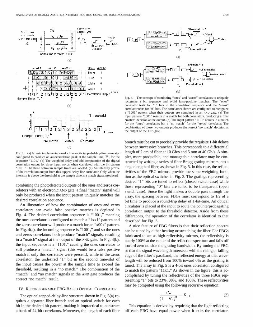
A common implementation of an optical correlator is thetapped delay line. A basic optical tapped delay line correlatoris shown in Fig. 3(a). The delay line is configured to match thecorrelation sequence “1101.” Thus, the delay line requires fourtaps (one for each bit in the desired sequence), weighted by thefactors 1, 1, 0, and 1, respectively. The weights are implementedby placing a switch in each path that is closed for weightand opened for weight . The incoming optical bitstream isequally split among the four fiber-optic delay lines. Each suc-cessive delay line adds one additional bit of delay to the in-coming signal before the combiner, where the powers of the foursignals are added to yield the correlation output function. Thisfunction is sampled at the optimum time and passed througha threshold detector that is set to detect a power level above two,since the autocorrelation peak of “1101” with itself equals three(or, more specifically, three times the power in each “1” bit).The output is detected using a photoreceiver, and a simple elec-tronic decision circuit is used to compare the correlation outputto the threshold value. The high-speed advantage of optics stillprevails in this case since the correlation function is produced inthe time it takes the signal to traverse the optical correlator. Thedecision circuit only needs to be triggered at the packet rate,which is often in the range of kHz to MHz, depending on thenumber of bits in each data packet. For example, for a stream of
short, 40-byte packets (320 bits/packet) at 40 Gb/s, the packetrate is only 125 MHz. The mathematical function describing thetapped-delay-line correlator is
(1)
where is the number of bits in the correlation sequence,is one bit period, is the input signal delayed by
bit times, and represents the weights that mul-tiply each of the -bit delayed input signals. For a phase-modu-lated system, the same operation is performed by replacing theswitches with the appropriate optical phase-shifters to match thedesired bit pattern (e.g., “ ” instead of “1101”). Fig. 3(b)illustrates the delay-and-add operation of the correlator for thecase when the three 4-bit words “1011,” “1101,” and “0101”are input to the correlator, where the second word is an exactmatch to the desired sequence. Since the correlation functionfor two 4-bit words is 7 bits long and the peak occurs duringthe fourth time slot, the correlation output is sampled every fourbits and compared to a threshold as shown in Fig. 3(c). As ex-pected, the correlation output for the second word exceeds thethreshold, while the first and third samples produce no matches.Note that for an input signal bits long, the length of the cor-relation output will be 1 bits long.
B. The Need for “Ones” and “Zeros” Correlators
Note that the correlator as shown in Fig. 3(a) will also pro-duce a level “3” peak that is above the threshold at timefora “1111” input, which is not the desired bit pattern. This is be-cause the open switch in the third delay line, corresponding tothe third correlation bit, does not “care” if the third bit is a “1”or a “0” since it does not pass any light. Thus, the correlator asshown is really configured to produce a match for the sequence“11x1” where the “x” indicates a “don’t care” bit that can eitherbe “0” or “1.”
This is not an issue in optical CDMA systems, where the setof codewords can be specifically designed to maintain a con-stant number of “1” bits in each codeword. However, for ourheader recognition application, which must be able to uniquelyrecognize any of the 2possible -bit sequences, this situationwill result in “false-positive” matches whenever a “1” is presentwhere a “0” bit is desired. To overcome this problem, we add asecond correlator that is configured in complement to the firstone and produces a “match” signal whenzeropower is presentat the sample time. This is accomplished by placing aNOT gateat the output of the threshold detector that is set just above levelzero. If the power goes above the threshold, this indicates that atleast one “1” bit is present where a “0” is desired, and theNOT
gate will convert the high output to a low one to indicate “nomatch” for this correlator. This correlator therefore correlateswith the desired “0” bits in the sequence and is thus called a“zeros” (or “0s”) correlator. Likewise, the originally describedcorrelator is called a “ones” (or “1s”) correlator. In the zeroscorrelator, the switches are closed for desired “0” bits and openotherwise (or, as explained in the next section, the FBG mir-rors reflect for desired “0” bits and are tuned away otherwise).Thus, the “1” bits are “don’t care” bits in a zeros correlator. By
HAUER et al.: OPTICALLY ASSISTED INTERNET ROUTING USING FBG-BASED CORRELATORS 2769
(a)
(b)
(c)
Fig. 3. (a) A basic implementation of a fiber-optic tapped-delay-line correlatorconfigured to produce an autocorrelation peak at the sample time,T , for thesequence “1101.” (b) The weighted delay-and-add computation of the digitalcorrelation output for three input words when correlated with the bit pattern“1101.” The three optimum sample times are labeled. (c) An intensity profileof the correlation output from this tapped-delay-line correlator. Only when theintensity is above the threshold at the sample time is a match signal produced.
combining the photodetected outputs of the ones and zeros cor-relators with an electronicAND gate, a final “match” signal willonly be produced when the input pattern uniquely matches thedesired correlation sequence.
An illustration of how the combination of ones and zeroscorrelators can avoid false positive matches is depicted inFig. 4. The desired correlation sequence is “1001,” meaningthe ones correlator is configured to match a “1xx1” pattern andthe zeros correlator will produce a match for an “x00x” pattern.In Fig. 4(a), the incoming sequence is “1001,” and so the onesand zeros correlators both produce “match” signals, resultingin a “match” signal at the output of theAND gate. In Fig. 4(b),the input sequence is a “1101,” causing the ones correlator tostill produce a “match” signal (this would be a false positivematch if only this correlator were present), while in the zeroscorrelator, the undesired “1” bit in the second time-slot ofthe input causes the power at the sample time to exceed thethreshold, resulting in a “no match.” The combination of the“match” and “no match” signals in theAND gate produces thecorrect “no match” result.
IV. RECONFIGURABLEFBG-BASED OPTICAL CORRELATOR
The optical tapped-delay-line structure shown in Fig. 3(a) re-quires a separate fiber branch and an optical switch for eachbit in the desired bit pattern, making it impractical to constructa bank of 24-bit correlators. Moreover, the length of each fiber
(a)
(b)
Fig. 4. The concept of combining “ones” and “zeros” correlators to uniquelyrecognize a bit sequence and avoid false-positive matches. The “ones”correlator tests for “1” bits in the correlation sequence and the “zeros”correlator tests for “0” bits. The correlators shown are configured to recognizea “1001” pattern when their outputs are combined in anAND gate. (a) Theinput pattern “1001” results in a match for both correlators, producing a final“match” decision at the output. (b) The input pattern “1101” results in a matchfor the “ones” correlators but a “no match” for the “zeros” correlator. Thecombination of these two outputs produces the correct “no match” decision atthe output of theAND gate.
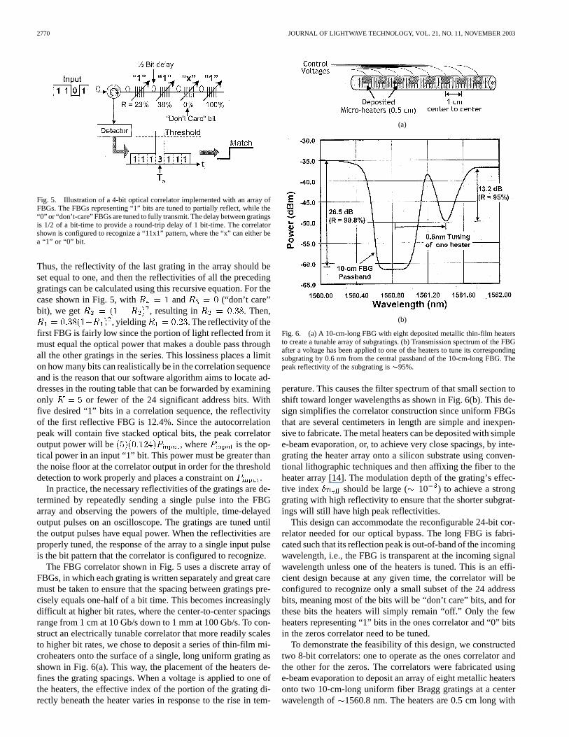
branch must be cut to precisely provide the requisite 1-bit delaysbetween successive branches. This corresponds to a differentiallength of 2 cm of fiber at 10 Gb/s and 5 mm at 40 Gb/s. A sim-pler, more producible, and manageable correlator may be con-structed by writing a series of fiber Bragg grating mirrors into asingle length of fiber, as shown in Fig. 5. In this case, the reflec-tivities of the FBG mirrors provide the same weighting func-tion as the optical switches in Fig. 3. The gratings representingdesired “1” bits are tuned to reflect (closed switch case) whilethose representing “0” bits are tuned to be transparent (openswitch case). Since the light makes a double pass through thearray, the spacing between FBGs must correspond to 1/2 of abit time to produce a round-trip delay of 1-bit-time. An opticalcirculator is placed at the input to route the counterpropagatingcorrelation output to the threshold detector. Aside from thesedifferences, the operation of the correlator is identical to thatdescribed for Fig. 3.
A nice feature of FBG filters is that their reflection spectracan be tuned by either heating or stretching the fiber. For FBGsfabricated to act as high-reflectivity mirrors, the reflectivity isnearly 100% at the center of the reflection spectrum and falls offtoward zero outside the grating bandwidth. By tuning the FBGso that the signal wavelength intersects with the rising or fallingedge of the filter’s passband, the reflected energy at that wave-length will be reduced from 100% toward 0% as the grating istuned. The array in Fig. 5 is a 4-bit ones correlator, configuredto match the pattern “11x1.” As shown in the figure, this is ac-complished by tuning the reflectivities of the three FBGs rep-resenting “1” bits to 23%, 38%, and 100%. These reflectivitiesmay be computed using the following recursive equation:
(2)
This equation is derived by requiring that the light reflectingoff each FBG have equal power when it exits the correlator.
2770 JOURNAL OF LIGHTWAVE TECHNOLOGY, VOL. 21, NO. 11, NOVEMBER 2003
Fig. 5. Illustration of a 4-bit optical correlator implemented with an array ofFBGs. The FBGs representing “1” bits are tuned to partially reflect, while the“0” or “don’t-care” FBGs are tuned to fully transmit. The delay between gratingsis 1/2 of a bit-time to provide a round-trip delay of 1 bit-time. The correlatorshown is configured to recognize a “11x1” pattern, where the “x” can either bea “1” or “0” bit.
Thus, the reflectivity of the last grating in the array should beset equal to one, and then the reflectivities of all the precedinggratings can be calculated using this recursive equation. For thecase shown in Fig. 5, with and (“don’t care”bit), we get , resulting in . Then,
, yielding . The reflectivity of thefirst FBG is fairly low since the portion of light reflected from itmust equal the optical power that makes a double pass throughall the other gratings in the series. This lossiness places a limiton how many bits can realistically be in the correlation sequenceand is the reason that our software algorithm aims to locate ad-dresses in the routing table that can be forwarded by examiningonly or fewer of the 24 significant address bits. Withfive desired “1” bits in a correlation sequence, the reflectivityof the first reflective FBG is 12.4%. Since the autocorrelationpeak will contain five stacked optical bits, the peak correlatoroutput power will be , where is the op-tical power in an input “1” bit. This power must be greater thanthe noise floor at the correlator output in order for the thresholddetection to work properly and places a constraint on .
In practice, the necessary reflectivities of the gratings are de-termined by repeatedly sending a single pulse into the FBGarray and observing the powers of the multiple, time-delayedoutput pulses on an oscilloscope. The gratings are tuned untilthe output pulses have equal power. When the reflectivities areproperly tuned, the response of the array to a single input pulseis the bit pattern that the correlator is configured to recognize.
The FBG correlator shown in Fig. 5 uses a discrete array ofFBGs, in which each grating is written separately and great caremust be taken to ensure that the spacing between gratings pre-cisely equals one-half of a bit time. This becomes increasinglydifficult at higher bit rates, where the center-to-center spacingsrange from 1 cm at 10 Gb/s down to 1 mm at 100 Gb/s. To con-struct an electrically tunable correlator that more readily scalesto higher bit rates, we chose to deposit a series of thin-film mi-croheaters onto the surface of a single, long uniform grating asshown in Fig. 6(a). This way, the placement of the heaters de-fines the grating spacings. When a voltage is applied to one ofthe heaters, the effective index of the portion of the grating di-rectly beneath the heater varies in response to the rise in tem-
(a)
(b)
Fig. 6. (a) A 10-cm-long FBG with eight deposited metallic thin-film heatersto create a tunable array of subgratings. (b) Transmission spectrum of the FBGafter a voltage has been applied to one of the heaters to tune its correspondingsubgrating by 0.6 nm from the central passband of the 10-cm-long FBG. Thepeak reflectivity of the subgrating is�95%.
perature. This causes the filter spectrum of that small section toshift toward longer wavelengths as shown in Fig. 6(b). This de-sign simplifies the correlator construction since uniform FBGsthat are several centimeters in length are simple and inexpen-sive to fabricate. The metal heaters can be deposited with simplee-beam evaporation, or, to achieve very close spacings, by inte-grating the heater array onto a silicon substrate using conven-tional lithographic techniques and then affixing the fiber to theheater array [14]. The modulation depth of the grating’s effec-tive index should be large ( 10 ) to achieve a stronggrating with high reflectivity to ensure that the shorter subgrat-ings will still have high peak reflectivities.
This design can accommodate the reconfigurable 24-bit cor-relator needed for our optical bypass. The long FBG is fabri-cated such that its reflection peak is out-of-band of the incomingwavelength, i.e., the FBG is transparent at the incoming signalwavelength unless one of the heaters is tuned. This is an effi-cient design because at any given time, the correlator will beconfigured to recognize only a small subset of the 24 addressbits, meaning most of the bits will be “don’t care” bits, and forthese bits the heaters will simply remain “off.” Only the fewheaters representing “1” bits in the ones correlator and “0” bitsin the zeros correlator need to be tuned.
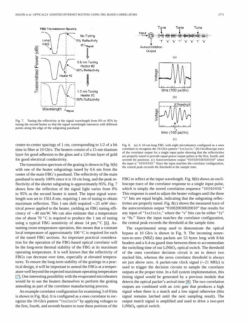
To demonstrate the feasibility of this design, we constructedtwo 8-bit correlators: one to operate as the ones correlator andthe other for the zeros. The correlators were fabricated usinge-beam evaporation to deposit an array of eight metallic heatersonto two 10-cm-long uniform fiber Bragg gratings at a centerwavelength of 1560.8 nm. The heaters are 0.5 cm long with
HAUER et al.: OPTICALLY ASSISTED INTERNET ROUTING USING FBG-BASED CORRELATORS 2771
Fig. 7. Tuning the reflectivity at the signal wavelength from 0% to 95% bytuning the second heater so that the signal wavelength intersects with differentpoints along the edge of the subgrating passband.
center-to-center spacings of 1 cm, corresponding to 1/2 of a bittime in fiber at 10 Gb/s. The heaters consist of a 15-nm titaniumlayer for good adhesion to the glass and a 120-nm layer of goldfor good electrical conductivity.
The transmission spectrum of the grating is shown in Fig. 6(b)with one of the heater subgratings tuned by 0.6 nm from thecenter of the main FBG’s passband. The reflectivity of the mainpassband is nearly 100% since it is 10 cm long, and the peak re-flectivity of the shorter subgrating is approximately 95%. Fig. 7shows how the reflection of the signal light varies from 0%to 95% as the second heater is tuned. The input signal wave-length was set to 1561.8 nm, requiring 1 nm of tuning to obtainmaximum reflection. This 1-nm shift required25 mW elec-trical power applied to the heater, yielding an FBG tuning effi-ciency of 40 nm/W. We can also estimate that a temperaturerise of about 70 C is required to produce the 1 nm of tuningusing a typical FBG sensitivity of about 14 pmC [6]. As-suming room-temperature operation, this means that a constantlocal temperature of approximately 100C is required for eachof the tuned FBG sections. An important practical considera-tion for the operation of the FBG-based optical correlator willbe the long-term thermal stability of the FBG at its maximumoperating temperature. It is well known that the reflectivity ofFBGs can decrease over time, especially at elevated tempera-tures. To ensure the long-term stability of the gratings in a prac-tical design, it will be important to anneal the FBGs at a temper-ature well beyond the expected maximum operating temperature[7]. One interesting possibility with the evaporated microheaterswould be to use the heaters themselves to perform the gratingannealing as part of the correlator manufacturing process.
An example correlator configuration for examining 3 of 8 bitsis shown in Fig. 8(a). It is configured as a ones correlator to rec-ognize the 10-Gb/s pattern “1xx1xx1x” by applying voltages tothe first, fourth, and seventh heaters to tune these portions of the
(a)
(b)
(c)
Fig. 8. (a) A 10-cm-long FBG with eight microheaters configured as a onescorrelator to recognize the 10-Gb/s pattern “1xx1xx1x.” (b) Oscilloscope traceof the correlator output for a single input pulse showing that the reflectivitiesare properly tuned to provide equal-power output pulses at the first, fourth, andseventh bit positions. (c) Autocorrelation output “010 020 030 020 010” whenthe input is “10 010 010.” Since the input matches the correlator configuration,the central peak exceeds the threshold at the sample time.
FBG to reflect at the input wavelength. Fig. 8(b) shows an oscil-loscope trace of the correlator response to a single input pulse,which is simply the stored correlation sequence “10 010 010.”This response is used to adjust the heater voltages until the three“1” bits are equal height, indicating that the subgrating reflec-tivites are properly tuned. Fig. 8(c) shows the measured trace ofthe autocorrelation output “010020030020010” that results forany input of “1xx1xx1x,” where the “x” bits can be either “1s”or “0s.” Since the input matches the correlator configuration,the central peak exceeds the threshold at the sample time.
The experimental setup used to demonstrate the opticalbypass at 10 Gb/s is shown in Fig. 9. The incoming nonre-turn-to-zero (NRZ) data packets are 53 bytes long with 8-bitheaders and a 6.4-ns guard time between them to accommodatethe switching time of our LiNbOoptical switch. The thresholdof the ones correlator decision circuit is set to detect twostacked bits, whereas the zeros correlator threshold is alwaysset just above zero. A packet-rate clock signal (21 MHz) isused to trigger the decision circuits to sample the correlatoroutputs at the proper time. In a full system implementation, thistiming signal would be generated by a previous module thatdetects the optical packet’s arrival time [8]. The two correlationoutputs are combined with anAND gate that produces a highsignal when there is a match and a low signal otherwise (thissignal remains latched until the next sampling result). Theoutput match signal is amplified and used to drive a two-portLiNbO optical switch.

2772 JOURNAL OF LIGHTWAVE TECHNOLOGY, VOL. 21, NO. 11, NOVEMBER 2003
Fig. 9. Experimental setup. The FBG heaters are tuned to configure the correlator to match any “xx1x01x0” pattern. The output of the electronicAND gate drivesa 2� 2 LiNbO optical switch and is set to switch packets with matching headers to port C and all others to port D.
To demonstrate the successful operation of the optical by-pass function, the FBG correlators were tuned to recognize an“xx1x01x0” pattern ( of 8 bits), and the correlation outputwas used to route packets with matching headers to port C ofthe two-port optical switch. The experimental results showingthe oscilloscope traces of the packets and switch control sig-nals are shown in Fig. 10. The input packet stream contains fourpackets with different headers, the second of which matches thecorrelator configuration. The second row shows the matchingsignal at the output of theAND gate, which is amplified andused to drive the optical switch. As expected, the output goeshigh during the second packet. The last two lines show the suc-cessful routing of the packet with a matching header to port Cand all nonmatching packets to port D.
The “lookup time” required to forward packets using theseoptical correlators is simply the time it takes for the light to prop-agate through the correlators and for the optical switch to flip,which is on the order of a few nanoseconds. Thus, the lookuptime for packets that are forwarded by the optical bypass is re-duced by an order of magnitude, from microseconds (for elec-tronic lookups) to nanoseconds, and is limited only by the op-tical switching time. As for the reconfiguration time of the ther-mally tuned FBG correlators, they will have a time constant ofabout 1 s, which is typical of thermally tuned all-fiber devices[9]. This slow reconfiguration time should not be a problem inpractice because the correlators are reconfigured only when therouting table is recomputed, which at worst occurs several timesper day. However, if faster reconfiguration times are desirable,etched cladding fibers can be used to produce significantly fastertuning speeds [14].
V. MULTIWAVELENGTH FBG CORRELATOR
The above method for optical header-subset recognition actson a single WDM channel, thus requiringcomplete modulesin order to recognize the headers ondifferent WDM chan-nels. A correlation module that enables reconfigurable opticalcorrelation of multiple WDM channels simultaneously can sig-nificantly reduce the number of components required in a WDMrouting node. Using a set of discrete sampled fiber Bragg grat-ings, a multiwavelength FBG correlator can be constructed. Asampled FBG is an FBG that has a superstructure written on top
Fig. 10. Experimental results showing the successful correlation andswitching of the matching packet to port C and all others to port D. The 6.4-nsguard time between packets is to allow for the switching time of the opticalswitch.
of the grating for which the Fourier transform produces a reflec-tive time delay that is replicated at equal wavelength spacings[10]. When this type of FBG is stretched or heated, the entirereflection spectrum shifts, causing the reflectivity at each wave-length to experience the same variation. Thus, the correlationsequence can be reconfigured for all incoming channels simul-taneously.
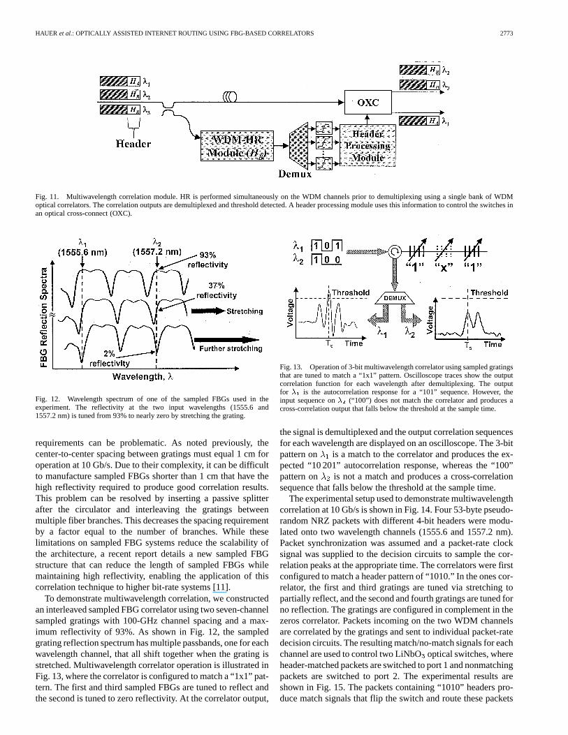
A conceptual diagram illustrating how a WDM header recog-nition (HR) module is employed in a routing node is shown inFig. 11. The module may still be used as an optical bypass for anInternet router, but in this case the packets on all incoming wave-lengths can simultaneously be compared to the entries in the op-tical lookup table. A portion of the incident light from the WDMchannels is tapped off and sent into the correlation module. Themodule uses a bank of tunable sampled-FBG arrays for com-paring the incoming packet addresses against a stored set ofpatterns. The correlator outputs are demultiplexed and separatedecision circuits are used to sample the output for each wave-length. The resulting match/no-match signals are used to controlan optical cross-connect to properly switch the packets on eachwavelength.
While a sampled FBG correlator can be constructed ina manner similar to a standard FBG correlator, the spacing
HAUER et al.: OPTICALLY ASSISTED INTERNET ROUTING USING FBG-BASED CORRELATORS 2773
Fig. 11. Multiwavelength correlation module. HR is performed simultaneously on the WDM channels prior to demultiplexing using a single bank of WDMoptical correlators. The correlation outputs are demultiplexed and threshold detected. A header processing module uses this information to control the switches inan optical cross-connect (OXC).
Fig. 12. Wavelength spectrum of one of the sampled FBGs used in theexperiment. The reflectivity at the two input wavelengths (1555.6 and1557.2 nm) is tuned from 93% to nearly zero by stretching the grating.
requirements can be problematic. As noted previously, thecenter-to-center spacing between gratings must equal 1 cm foroperation at 10 Gb/s. Due to their complexity, it can be difficultto manufacture sampled FBGs shorter than 1 cm that have thehigh reflectivity required to produce good correlation results.This problem can be resolved by inserting a passive splitterafter the circulator and interleaving the gratings betweenmultiple fiber branches. This decreases the spacing requirementby a factor equal to the number of branches. While theselimitations on sampled FBG systems reduce the scalability ofthe architecture, a recent report details a new sampled FBGstructure that can reduce the length of sampled FBGs whilemaintaining high reflectivity, enabling the application of thiscorrelation technique to higher bit-rate systems [11].
To demonstrate multiwavelength correlation, we constructedan interleaved sampled FBG correlator using two seven-channelsampled gratings with 100-GHz channel spacing and a max-imum reflectivity of 93%. As shown in Fig. 12, the sampledgrating reflection spectrum has multiple passbands, one for eachwavelength channel, that all shift together when the grating isstretched. Multiwavelength correlator operation is illustrated inFig. 13, where the correlator is configured to match a “1x1” pat-tern. The first and third sampled FBGs are tuned to reflect andthe second is tuned to zero reflectivity. At the correlator output,
Fig. 13. Operation of 3-bit multiwavelength correlator using sampled gratingsthat are tuned to match a “1x1” pattern. Oscilloscope traces show the outputcorrelation function for each wavelength after demultiplexing. The outputfor � is the autocorrelation response for a “101” sequence. However, theinput sequence on� (“100”) does not match the correlator and produces across-correlation output that falls below the threshold at the sample time.
the signal is demultiplexed and the output correlation sequencesfor each wavelength are displayed on an oscilloscope. The 3-bitpattern on is a match to the correlator and produces the ex-pected “10 201” autocorrelation response, whereas the “100”pattern on is not a match and produces a cross-correlationsequence that falls below the threshold at the sample time.
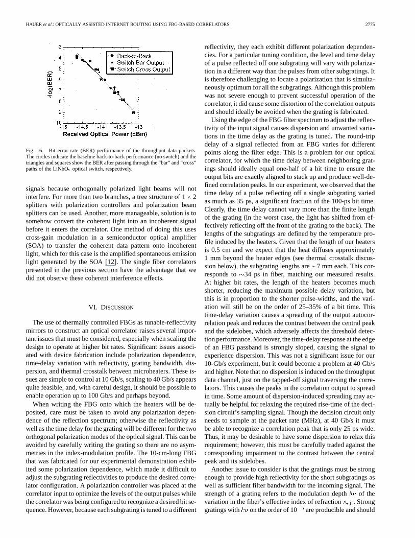
The experimental setup used to demonstrate multiwavelengthcorrelation at 10 Gb/s is shown in Fig. 14. Four 53-byte pseudo-random NRZ packets with different 4-bit headers were modu-lated onto two wavelength channels (1555.6 and 1557.2 nm).Packet synchronization was assumed and a packet-rate clocksignal was supplied to the decision circuits to sample the cor-relation peaks at the appropriate time. The correlators were firstconfigured to match a header pattern of “1010.” In the ones cor-relator, the first and third gratings are tuned via stretching topartially reflect, and the second and fourth gratings are tuned forno reflection. The gratings are configured in complement in thezeros correlator. Packets incoming on the two WDM channelsare correlated by the gratings and sent to individual packet-ratedecision circuits. The resulting match/no-match signals for eachchannel are used to control two LiNbOoptical switches, whereheader-matched packets are switched to port 1 and nonmatchingpackets are switched to port 2. The experimental results areshown in Fig. 15. The packets containing “1010” headers pro-duce match signals that flip the switch and route these packets
2774 JOURNAL OF LIGHTWAVE TECHNOLOGY, VOL. 21, NO. 11, NOVEMBER 2003
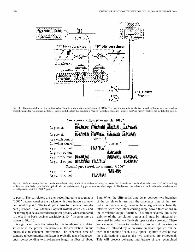
Fig. 14. Experimental setup for multiwavelength optical correlation using sampled FBGs. The decision outputs for the two wavelength channels are used ascontrol signals for two optical switches. Packets with headers that produce a “match” signal are switched to port 1 and “no-match” packets are switched to port 2.
Fig. 15. Multiwavelength header correlation and switching results. Four packets incoming on two WDM channels are correlated with the pattern “1010.” Matchingpackets are switched to port 1 of the optical switches and nonmatching packets are switched to port 2. The last two rows show the results when the correlators arereconfigured to match a “1000” pattern.
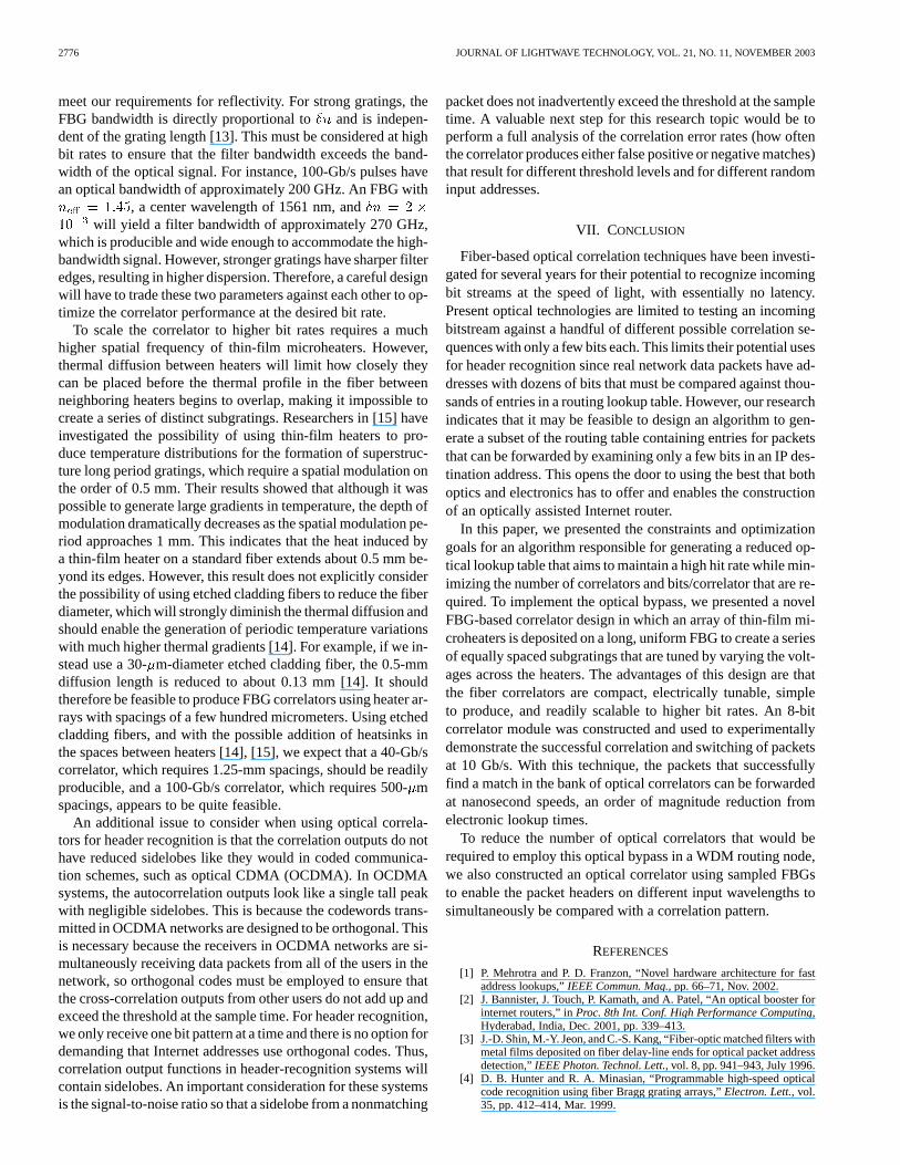
to port 1. The correlators are then reconfigured to recognize a“1000” pattern, causing the packets with these headers to nowbe routed to port 1. The total optical loss for the data through-path (90% tap + AWG demux + optical switch) was 7.7 dB, andthe throughput data suffered zero power penalty when comparedto the back-to-back receiver sensitivity at 10bit error rate, asshown in Fig. 16.
A significant issue that arises for this interleaved correlatorstructure is the power fluctuations in the correlation outputpulses due to coherent interference. The coherence time ofstandard telecommunication lasers is typically tens of nanosec-onds, corresponding to a coherence length in fiber of about
2 m. When the differential time delay between two branchesof the correlator is less than the coherence time of the laser(which is the case here), the recombined signals will coherentlyinterfere with each other causing large power fluctuations inthe correlation output function. This effect severely limits thestability of the correlation output and must be mitigated orprevented in order to effectively operate the correlator. Thereare a number of ways to resolve this problem. A polarizationcontroller followed by a polarization beam splitter can beused at the input of each 12 optical splitter to ensure thatthe polarizations between the two branches are orthogonal.This will prevent coherent interference of the recombined
HAUER et al.: OPTICALLY ASSISTED INTERNET ROUTING USING FBG-BASED CORRELATORS 2775
Fig. 16. Bit error rate (BER) performance of the throughput data packets.The circles indicate the baseline back-to-back performance (no switch) and thetriangles and squares show the BER after passing through the “bar” and “cross”paths of the LiNbO optical switch, respectively.
signals because orthogonally polarized light beams will notinterfere. For more than two branches, a tree structure of 12splitters with polarization controllers and polarization beamsplitters can be used. Another, more manageable, solution is tosomehow convert the coherent light into an incoherent signalbefore it enters the correlator. One method of doing this usescross-gain modulation in a semiconductor optical amplifier(SOA) to transfer the coherent data pattern onto incoherentlight, which for this case is the amplified spontaneous emissionlight generated by the SOA [12]. The single fiber correlatorspresented in the previous section have the advantage that wedid not observe these coherent interference effects.
VI. DISCUSSION
The use of thermally controlled FBGs as tunable-reflectivitymirrors to construct an optical correlator raises several impor-tant issues that must be considered, especially when scaling thedesign to operate at higher bit rates. Significant issues associ-ated with device fabrication include polarization dependence,time-delay variation with reflectivity, grating bandwidth, dis-persion, and thermal crosstalk between microheaters. These is-sues are simple to control at 10 Gb/s, scaling to 40 Gb/s appearsquite feasible, and, with careful design, it should be possible toenable operation up to 100 Gb/s and perhaps beyond.
When writing the FBG onto which the heaters will be de-posited, care must be taken to avoid any polarization depen-dence of the reflection spectrum; otherwise the reflectivity aswell as the time delay for the grating will be different for the twoorthogonal polarization modes of the optical signal. This can beavoided by carefully writing the grating so there are no asym-metries in the index-modulation profile. The 10-cm-long FBGthat was fabricated for our experimental demonstration exhib-ited some polarization dependence, which made it difficult toadjust the subgrating reflectivities to produce the desired corre-lator configuration. A polarization controller was placed at thecorrelator input to optimize the levels of the output pulses whilethe correlator was being configured to recognize a desired bit se-quence. However, because each subgrating is tuned to a different
reflectivity, they each exhibit different polarization dependen-cies. For a particular tuning condition, the level and time delayof a pulse reflected off one subgrating will vary with polariza-tion in a different way than the pulses from other subgratings. Itis therefore challenging to locate a polarization that is simulta-neously optimum for all the subgratings. Although this problemwas not severe enough to prevent successful operation of thecorrelator, it did cause some distortion of the correlation outputsand should ideally be avoided when the grating is fabricated.
Using the edge of the FBG filter spectrum to adjust the reflec-tivity of the input signal causes dispersion and unwanted varia-tions in the time delay as the grating is tuned. The round-tripdelay of a signal reflected from an FBG varies for differentpoints along the filter edge. This is a problem for our opticalcorrelator, for which the time delay between neighboring grat-ings should ideally equal one-half of a bit time to ensure theoutput bits are exactly aligned to stack up and produce well-de-fined correlation peaks. In our experiment, we observed that thetime delay of a pulse reflecting off a single subgrating variedas much as 35 ps, a significant fraction of the 100-ps bit time.Clearly, the time delay cannot vary more than the finite lengthof the grating (in the worst case, the light has shifted from ef-fectively reflecting off the front of the grating to the back). Thelengths of the subgratings are defined by the temperature pro-file induced by the heaters. Given that the length of our heatersis 0.5 cm and we expect that the heat diffuses approximately1 mm beyond the heater edges (see thermal crosstalk discus-sion below), the subgrating lengths are7 mm each. This cor-responds to 34 ps in fiber, matching our measured results.At higher bit rates, the length of the heaters becomes muchshorter, reducing the maximum possible delay variation, butthis is in proportion to the shorter pulse-widths, and the vari-ation will still be on the order of 25–35% of a bit time. Thistime-delay variation causes a spreading of the output autocor-relation peak and reduces the contrast between the central peakand the sidelobes, which adversely affects the threshold detec-tion performance. Moreover, the time-delay response at the edgeof an FBG passband is strongly sloped, causing the signal toexperience dispersion. This was not a significant issue for our10-Gb/s experiment, but it could become a problem at 40 Gb/sand higher. Note that no dispersion is induced on the throughputdata channel, just on the tapped-off signal traversing the corre-lators. This causes the peaks in the correlation output to spreadin time. Some amount of dispersion-induced spreading may ac-tually be helpful for relaxing the required rise-time of the deci-sion circuit’s sampling signal. Though the decision circuit onlyneeds to sample at the packet rate (MHz), at 40 Gb/s it mustbe able to recognize a correlation peak that is only 25 ps wide.Thus, it may be desirable to have some dispersion to relax thisrequirement; however, this must be carefully traded against thecorresponding impairment to the contrast between the centralpeak and its sidelobes.
Another issue to consider is that the gratings must be strongenough to provide high reflectivity for the short subgratings aswell as sufficient filter bandwidth for the incoming signal. Thestrength of a grating refers to the modulation depthof thevariation in the fiber’s effective index of refraction . Stronggratings with on the order of 10 are producible and should
2776 JOURNAL OF LIGHTWAVE TECHNOLOGY, VOL. 21, NO. 11, NOVEMBER 2003
meet our requirements for reflectivity. For strong gratings, theFBG bandwidth is directly proportional to and is indepen-dent of the grating length [13]. This must be considered at highbit rates to ensure that the filter bandwidth exceeds the band-width of the optical signal. For instance, 100-Gb/s pulses havean optical bandwidth of approximately 200 GHz. An FBG with
, a center wavelength of 1561 nm, andwill yield a filter bandwidth of approximately 270 GHz,
which is producible and wide enough to accommodate the high-bandwidth signal. However, stronger gratings have sharper filteredges, resulting in higher dispersion. Therefore, a careful designwill have to trade these two parameters against each other to op-timize the correlator performance at the desired bit rate.
To scale the correlator to higher bit rates requires a muchhigher spatial frequency of thin-film microheaters. However,thermal diffusion between heaters will limit how closely theycan be placed before the thermal profile in the fiber betweenneighboring heaters begins to overlap, making it impossible tocreate a series of distinct subgratings. Researchers in [15] haveinvestigated the possibility of using thin-film heaters to pro-duce temperature distributions for the formation of superstruc-ture long period gratings, which require a spatial modulation onthe order of 0.5 mm. Their results showed that although it waspossible to generate large gradients in temperature, the depth ofmodulation dramatically decreases as the spatial modulation pe-riod approaches 1 mm. This indicates that the heat induced bya thin-film heater on a standard fiber extends about 0.5 mm be-yond its edges. However, this result does not explicitly considerthe possibility of using etched cladding fibers to reduce the fiberdiameter, which will strongly diminish the thermal diffusion andshould enable the generation of periodic temperature variationswith much higher thermal gradients [14]. For example, if we in-stead use a 30-m-diameter etched cladding fiber, the 0.5-mmdiffusion length is reduced to about 0.13 mm [14]. It shouldtherefore be feasible to produce FBG correlators using heater ar-rays with spacings of a few hundred micrometers. Using etchedcladding fibers, and with the possible addition of heatsinks inthe spaces between heaters [14], [15], we expect that a 40-Gb/scorrelator, which requires 1.25-mm spacings, should be readilyproducible, and a 100-Gb/s correlator, which requires 500-mspacings, appears to be quite feasible.
An additional issue to consider when using optical correla-tors for header recognition is that the correlation outputs do nothave reduced sidelobes like they would in coded communica-tion schemes, such as optical CDMA (OCDMA). In OCDMAsystems, the autocorrelation outputs look like a single tall peakwith negligible sidelobes. This is because the codewords trans-mitted in OCDMA networks are designed to be orthogonal. Thisis necessary because the receivers in OCDMA networks are si-multaneously receiving data packets from all of the users in thenetwork, so orthogonal codes must be employed to ensure thatthe cross-correlation outputs from other users do not add up andexceed the threshold at the sample time. For header recognition,we only receive one bit pattern at a time and there is no option fordemanding that Internet addresses use orthogonal codes. Thus,correlation output functions in header-recognition systems willcontain sidelobes. An important consideration for these systemsis the signal-to-noise ratio so that a sidelobe from a nonmatching
packet does not inadvertently exceed the threshold at the sampletime. A valuable next step for this research topic would be toperform a full analysis of the correlation error rates (how oftenthe correlator produces either false positive or negative matches)that result for different threshold levels and for different randominput addresses.
VII. CONCLUSION
Fiber-based optical correlation techniques have been investi-gated for several years for their potential to recognize incomingbit streams at the speed of light, with essentially no latency.Present optical technologies are limited to testing an incomingbitstream against a handful of different possible correlation se-quences with only a few bits each. This limits their potential usesfor header recognition since real network data packets have ad-dresses with dozens of bits that must be compared against thou-sands of entries in a routing lookup table. However, our researchindicates that it may be feasible to design an algorithm to gen-erate a subset of the routing table containing entries for packetsthat can be forwarded by examining only a few bits in an IP des-tination address. This opens the door to using the best that bothoptics and electronics has to offer and enables the constructionof an optically assisted Internet router.
In this paper, we presented the constraints and optimizationgoals for an algorithm responsible for generating a reduced op-tical lookup table that aims to maintain a high hit rate while min-imizing the number of correlators and bits/correlator that are re-quired. To implement the optical bypass, we presented a novelFBG-based correlator design in which an array of thin-film mi-croheaters is deposited on a long, uniform FBG to create a seriesof equally spaced subgratings that are tuned by varying the volt-ages across the heaters. The advantages of this design are thatthe fiber correlators are compact, electrically tunable, simpleto produce, and readily scalable to higher bit rates. An 8-bitcorrelator module was constructed and used to experimentallydemonstrate the successful correlation and switching of packetsat 10 Gb/s. With this technique, the packets that successfullyfind a match in the bank of optical correlators can be forwardedat nanosecond speeds, an order of magnitude reduction fromelectronic lookup times.
To reduce the number of optical correlators that would berequired to employ this optical bypass in a WDM routing node,we also constructed an optical correlator using sampled FBGsto enable the packet headers on different input wavelengths tosimultaneously be compared with a correlation pattern.
REFERENCES
[1] P. Mehrotra and P. D. Franzon, “Novel hardware architecture for fastaddress lookups,”IEEE Commun. Mag., pp. 66–71, Nov. 2002.
[2] J. Bannister, J. Touch, P. Kamath, and A. Patel, “An optical booster forinternet routers,” inProc. 8th Int. Conf. High Performance Computing,Hyderabad, India, Dec. 2001, pp. 339–413.
[3] J.-D. Shin, M.-Y. Jeon, and C.-S. Kang, “Fiber-optic matched filters withmetal films deposited on fiber delay-line ends for optical packet addressdetection,”IEEE Photon. Technol. Lett., vol. 8, pp. 941–943, July 1996.
[4] D. B. Hunter and R. A. Minasian, “Programmable high-speed opticalcode recognition using fiber Bragg grating arrays,”Electron. Lett., vol.35, pp. 412–414, Mar. 1999.
HAUER et al.: OPTICALLY ASSISTED INTERNET ROUTING USING FBG-BASED CORRELATORS 2777
[5] J. E. McGeehan, S. Kumar, J. Bannister, J. Touch, and A. E. Willner,“Optical time-to-live decrementing and subsequent dropping of an op-tical packet,” inProc. Opt. Fiber Commun. Conf., Mar. 2003, FS6.
[6] A. Othonos and K. Kalli,Fiber Bragg Gratings: Fundamentals and Ap-plications in Telecommunications and Sensing. Boston, MA: ArtechHouse, 1999, p. 99.
[7] R. Kashyap,Fiber Bragg Gratings. San Diego, CA: Academic, 1999,pp. 436–440.
[8] M. C. Cardakli and A. E. Willner, “Synchronization of a network ele-ment for optical packet switching using optical correlators and wave-length shifting,”IEEE Photon. Technol. Lett., vol. 14, pp. 1375–1377,Sept. 2002.
[9] L. Li, J. Geng, L. Zhao, G. Chen, G. Chen, Z. Fang, and C. F. Lam, “Re-sponse characteristics of thin-film-heated tunable fiber Bragg gratings,”IEEE Photon. Technol. Lett., vol. 15, pp. 545–547, Apr. 2003.
[10] M. Ibsen, M. K. Durkin, M. J. Cole, and R. I. Laming, “Sinc-sampledfiber Bragg gratings for identical multiple wavelength operation,”IEEEPhoton. Technol. Lett., vol. 10, pp. 842–844, June 1998.
[11] N. Yusuki and Y. Shinji, “Realization of various superstructure fiberBragg gratings for DWDM systems using multiple-phase-shift tech-nique,” inProc. Opt. Fiber Commun. Conf., Mar. 2002, TuQ3.
[12] P. Parolari, L. Marazzi, D. Rossetti, G. Maier, and M. Martinelli, “Co-herent-to-incoherent light conversion for optical correlators,”J. Light-wave Technol., vol. 18, pp. 1284–1288, Sept. 2000.
[13] T. Erdogan, “Fiber grating spectra,”J. Lightwave Technol., vol. 15, pp.1277–1294, Aug. 1997.
[14] E. R. Lyons, “Tunable all-fiber devices for optical fiber communica-tions,” Ph.D. dissertation, Univ. of California, Irvine, 2001.
[15] J. A. Rogers, P. Kuo, A. Ahuja, B. J. Eggleton, and R. J. Jackman,“Characteristics of heat flow in optical fiber devices that use integratedthin-film heaters,”Appl. Opt., vol. 39, pp. 5109–5116, Oct. 2000.
[16] G. G. Finn, S. Hotz, and C. Rogers, “Method and networking interfacelogic for providing embedded checksums,” U.S. Patent 5 826 032, Oct.20, 1998.
Michelle C. Hauer (S’96) received the B.S. degree in engineering physics fromLoyola Marymount University, Los Angeles, CA, in 1997 and the M.S.E.E. de-gree from the University of Southern California (USC), Los Angeles, in 2000,where she is currently pursing the doctoral degree.
She is currently a Research Assistant in the Optical Fiber CommunicationsLaboratory, USC. She is also a Systems Engineer for Raytheon Space andAirborne Systems, El Segundo, California. Her research interests includeoptical signal-processing techniques for implementing all-optical networkingfunctions, polarization effects in lightwave systems, and quantum communica-tions. She is a contributing author on more than 20 research papers.
Ms. Hauer is a Member of Tau Beta Pi, Eta Kappa Nu, and Sigma Pi Sigma.She is a Student Member of IEEE LEOS, the Optical Society of America (OSA),and SPS.
John E. McGeehan(S’96) received the B.S. and M.S. degrees in electricalengineering from the University of Southern California (USC), Los Angeles, in1998 and 2001, respectively, where he is currently pursuing the Ph.D. degree.
He joined the Optical Communications Laboratory, USC, as a Research As-sistant in 2001. His research interests include the implementation of all-opticalnetworking functions and optical signal processing as well as Raman amplifica-tion and signal monitoring. He is the author or coauthor of 12 technical papers
Saurabh Kumar (S’03) received the B.E. degree inelectrical and electronics engineering from the BirlaInstitute of Technology and Science, Pilani, India, in2001. He is currently pursuing the Ph.D. degree inelectrical engineering at the University of SouthernCalifornia (USC), Los Angeles.
He is a Research Assistant in the Optical Commu-nications Laboratory, USC. His research focuses onall-optical signal processing to enable the implemen-tation of networking functions in the optical domain.
Mr. Kumar is a Member of Eta Kappa Nu and aStudent Member of OSA.
Joseph D. Touch(S’84–M’91–SM’02) received theB.S. degree (Hons.) in biophysics and computer sci-ence from the University of Scranton, Scranton, PA,in 1985, the M.S. degree from Cornell University,Ithaca, NY, in 1987, and the Ph.D. degree from theUniversity of Pennsylvania, Philadelphia, in 1992,both in computer science.
He joined the USC/Information Sciences Institute,Marina del Rey, CA, in 1992 and is currently Directorof the Postel Center for Experimental Networking inthe Computer Networks Division. He is currently in-
volved with fault-tolerant networks such as DynaBone, NetFS, and X-Tend),optical Internet wide-area networks (WANs) and local-area networks (LANs)such as POW and OCDMA, geographic routing such as GeoNet, and smartspace devices for user presence. He has led projects ranging from gigabit LANs(such as ATOMIC2), NIC design (such as PC-ATOMIC), multicast web caching(I.SAM), to his most recent past project in the automated deployment and man-agement of virtual networks (XBONE). He is also a Research Associate Pro-fessor in the Department of Computer Science, University of Southern Cali-fornia, where he taught advanced operating systems for several years. He nowruns a program for summer students (SGREP) and advises a number of grad-uate students. He has several patents current and pending and is the author of anumber of publications, including the bookHigh Speed Networking: A System-atic Approach to High-Bandwidth Low-Latency Communication. His primaryresearch interests include virtual networks, automated network management,high-speed protocols, empirical protocol performance analysis, Internet archi-tecture, and protocols for latency reduction.
Dr. Touch is a Member of Sigma Xi (A’84–M’93) and ACM (S’83–M’92),Co-Chair of the IEEE ITC (Internet) committee, and is active in the IETF. Healso serves on the editorial boards of IEEE NETWORK and Elsevier’sComputerNetworks, and is a Member of several program committees, including IEEE IN-FOCOM (since 1994) and Sigcomm, and was Vice General Chair of Opticomm2001.
Joseph Bannister(S’80–M’80–SM’95) received theB.A. degree (with high distinction) in mathematicsfrom the University of Virginia, Richmond, in 1977and the M.S. degree in electrical engineering and theM.S. and Ph.D. degrees in computer science from theUniversity of California, Los Angeles, in 1980, 1984,and 1989, respectively.
He previously held positions at The AerospaceCorporation, System Development Corporation(now Unisys), Sytek (now Hughes Network Sys-tems), Research Triangle Institute, and Xerox. He
is currently a Director of the Computer Networks Division, InformationSciences Institute, and a Research Associate Professor in the Department ofElectrical Engineering-Systems for the University of Southern California inLos Angeles. His current technical interests are in high-speed and opticalnetworking, routing, network management and design, performance evaluation,and protocol engineering. He has more than 50 publications in high-speednetworking, distributed computing, and network management. He serves onthe editorial boards ofOptical NetworksandComputer Networks.
Dr. Bannister is a Member of Sigma Xi, the Association for Computing Ma-chinery (ACM) SIGCOMM, the Internet Society, and the American Associa-tion for the Advancement of Science (AAAS). He actively participates in theresearch community, serving or having served on the program committees oras Chair of INFOCOM, Interop, ICNP, ICCCN, LAN/MAN Workshop, OPTI-COMM, and the IEEE/TCCC Computer Communications Workshop. He is orhas been the Principal Investigator of the Defense Advanced Research ProjectsAgency (DARPA) and National Science Foundation (NSF) projects on decen-tralized network management, metacomputing, optical networks, quality of ser-vice management, wireless communications, satellite communications, battle-field awareness and data dissemination, lambda grids, and network vulnerabilityanalysis. In 1996, he participated on a DARPA ISAT Study Group on NetworkSurvivability, which resulted in the establishment of a major DARPA programin information assurance and survivability. In 2000 and 2003, he served on theNSF CISE ANIR Committee of Visitors, which was responsible for reviewingthe foundation’s research program in networking. He is currently serving a termon the NSF CISE Advisory Committee, advising the CISE Assistant Director onmatters related to the division’s research portfolio. He also co-chaired a panelon developing DARPA’s long-term networking and communications researchand development strategy. He has supported NSF, DARPA, and DOE on sourceselections, review panels, and other advisory tasks.
2778 JOURNAL OF LIGHTWAVE TECHNOLOGY, VOL. 21, NO. 11, NOVEMBER 2003
Edward R. Lyons (M’84) received the B.S. degree from the University of Cali-fornia, Los Angeles, in 1983 and the M.S. and Ph.D. degrees from the Universityof California at Irvine in 1994 and 2001, respectively.
He has more than 15 years of experience at Raytheon Space and AirborneSystems and Hughes Aircraft Company working on electrooptical and pho-tonic systems. Since 1987, he has been involved in photonics systems devel-opment at Hughes and Raytheon sites throughout southern California. Photonicprojects include work on secure fiber-optic communications systems, packagingof LiNbO modulators, and numerous programs involving high-performanceanalog fiber-optic link development. His research interests include tunable all-fiber devices and quantum communications.
C. H. Lin, photograph and biography not available at the time of publication.
A. A. Au, photograph and biography not available at the time of publication.
H. P. Lee, photograph and biography not available at the time of publication.
Dmitry S. Starodubov (M’03) received the M.Sc.degree in optical engineering from the Moscow Insti-tute of Radioengineering, Electronics and Automa-tion, Russia, in 1992 and the Ph.D. degree in laserphysics from the General Physics Institute, RussianAcademy of Sciences, in 1995.
He received a grant from the National ResearchCouncil and was a CAST Fellow at the Universityof Southern California from 1996 to 1997. In 1998,he cofounded Sabeus (formerly D-STAR Technolo-gies), where he presently serves as the Chief Tech-
nology Officer. His research interests include the physics of glasses, nonlinearoptics, optical communications, and fiber sensors. He is an author of 15 patentsand more than 100 publications.
Alan Eli Willner (S’87–M’88–SM’93–F’04)received the B.A. degree from Yeshiva University,New York, and the Ph.D. degree in electricalengineering from Columbia University, New York.
He has been with AT&T Bell Labs and Bellcore,and is a Professor of electrical engineering atthe University of Southern California. He wasPhotonics Division Chair of OSA; Program Cochairof the OSA Annual Meeting; Program Cochair ofCLEO; Steering and Technical Committee of OFC,Program committee member of ECOC. He has more
than 300 publications, including one book. His research is in optical fibercommunication systems.
Prof. Willner is a Fellow of the Optical Society of America (OSA) and wasa Fellow of the Semiconductor Research Corporation. He has received theNSF Presidential Faculty Fellows Award from the White House; the David andLucile Packard Foundation Fellowship; the NSF National Young InvestigatorAward; the Fulbright Foundation Senior Scholar Award; the IEEE LEOS Dis-tinguished Lecturer Award; the USC/Northrop Outstanding Junior EngineeringFaculty Research Award; the USC/TRW Best Engineering Teacher Award;and the Armstrong Foundation Memorial Prize. He was Vice-President forTechnical Affairs for IEEE LEOS; a member of the LEOS Board of Governors;Cochair of the OSA Science and Engineering Council; General Chair of theIEEE LEOS Annual Meeting; Editor-in-Chief of the JOURNAL OF LIGHTWAVE
TECHNOLOGY; Editor-in-Chief of the IEEE JOURNAL OF SELECTED TOPICS
IN QUANTUM ELECTRONICS; Guest Editor of the JOURNAL OF LIGHTWAVE
TECHNOLOGY Special Issue on wavelength-division multiplexing; and GuestEditor of the IEEE JOURNAL OF QUANTUM ELECTRONICS.