An integrated microfluidic device for two-dimensional combinatorial dilution
Upload
khangminh22Category
view
0download
0
Master thesis Thesis in Electronics, 30 credits
Optical Detector for Microfluidics
Master's Programme in Electronics Design, 60 credits
Halmstad 2022-05-22
Carlos Gomez Jimenez, Jaime Gomez Jimenez

ii

A B S T R A C T
This project arose from the need to filter the sampled data and eliminate non-useful information in Serial Crystallography in Microfluidic Device (MFD)by using a portable optical detector placed around the channel. By testingsixteen different configurations, always using an LED as a source and aphotodiode as a light sensor, changes in the channel due to the passageof air bubbles were detected. These changes corresponded to a 13,25% inrelation to the changes due to light switching, with a gain factor of 10,11
V/V. However, it was not sensitive enough to detect when a microcrystalpassed through it, although it can detect bubbles and opens the door todesign such sensors for these applications in the future.
Keywords— Serial crystallography, Microfluidic device, Optical detector, Particlecounting
iii

iv

A C K N O W L E D G E M E N T S
This project has been made possible thanks to the support and help of severalpeople. First of all, since we are siblings, completing this master’s degree has beenpossible thanks to our parents and grandparents, who have always been by ourside even from a distance.Secondly, we would like to thank Ross Friel for his excellent performance as thesissupervisor and interest in the project. He provided us with contact to other labswhere great people work: David and Joakim. We would especially like to thank thelatter for his help within Fablab Halmstad, where we have learned and developednew skills.We gratefully acknowledge that this project was possible as part of the "AdaptoCell"project, supported by the Swedish Foundation for Strategic Research, grant ITM-0375. Specifically, Monika was our support with the Biological part of our projectand made it possible to work far from the synchrotron.Finally, Per and Peo have been very helpful and always willing to share theirknowledge with anyone who needs it.
v

vi
C O N T E N T S
1 Introduction 1
1.1 Motivation . . . . . . . . . . . . . . . . . . . . . . . . . . . . . . . . . . 1
1.2 Goals . . . . . . . . . . . . . . . . . . . . . . . . . . . . . . . . . . . . . 2
2 Background 5
2.1 X-ray crystallography . . . . . . . . . . . . . . . . . . . . . . . . . . . 5
2.2 Microfluidic devices . . . . . . . . . . . . . . . . . . . . . . . . . . . . 6
2.3 Particle counting . . . . . . . . . . . . . . . . . . . . . . . . . . . . . . 10
2.3.1 Optical detectors . . . . . . . . . . . . . . . . . . . . . . . . . 10
2.3.2 Electromechanical detectors . . . . . . . . . . . . . . . . . . . 10
2.3.3 Comparison . . . . . . . . . . . . . . . . . . . . . . . . . . . . 13
3 Methods 15
3.1 Resources . . . . . . . . . . . . . . . . . . . . . . . . . . . . . . . . . . 15
3.1.1 Software . . . . . . . . . . . . . . . . . . . . . . . . . . . . . . 15
3.1.2 Electronic equipment . . . . . . . . . . . . . . . . . . . . . . . 15
3.1.3 Offline Setup . . . . . . . . . . . . . . . . . . . . . . . . . . . . 16
3.2 Detection approach . . . . . . . . . . . . . . . . . . . . . . . . . . . . 19
3.2.1 Different setups . . . . . . . . . . . . . . . . . . . . . . . . . . 19
3.2.2 Noise filtering . . . . . . . . . . . . . . . . . . . . . . . . . . . 20
3.2.3 Amplification . . . . . . . . . . . . . . . . . . . . . . . . . . . 20
3.3 Simulations . . . . . . . . . . . . . . . . . . . . . . . . . . . . . . . . . 20
3.3.1 Low Pass Filter . . . . . . . . . . . . . . . . . . . . . . . . . . 21
3.3.2 PIN with Fibre adapter Simulation . . . . . . . . . . . . . . . 23
3.3.3 Plain PIN Simulation . . . . . . . . . . . . . . . . . . . . . . . 24
3.4 Experimental . . . . . . . . . . . . . . . . . . . . . . . . . . . . . . . . 26
3.4.1 Chosen components . . . . . . . . . . . . . . . . . . . . . . . 26
3.4.2 Final arrangement . . . . . . . . . . . . . . . . . . . . . . . . . 27
4 Results 39
4.1 Mechanical results . . . . . . . . . . . . . . . . . . . . . . . . . . . . . 39
4.1.1 PCBs . . . . . . . . . . . . . . . . . . . . . . . . . . . . . . . . 39
4.1.2 Structures . . . . . . . . . . . . . . . . . . . . . . . . . . . . . 40
4.2 Data from different setups . . . . . . . . . . . . . . . . . . . . . . . . 42
4.2.1 Alignment . . . . . . . . . . . . . . . . . . . . . . . . . . . . . 43
4.2.2 Crystals measurements . . . . . . . . . . . . . . . . . . . . . . 45
4.2.3 Setup 1: Plain LED and plain PIN diode . . . . . . . . . . . . 46
4.2.4 Setup 2: Plain LED and PIN diode with fibre adapter . . . . 50
4.2.5 Setup 3: LED with fibre adapter and plain PIN diode . . . . 51
4.2.6 Setup 4: LED and PIN diode with fibre adapter . . . . . . . 55
4.3 Direct connections . . . . . . . . . . . . . . . . . . . . . . . . . . . . . 56
4.4 Microcontroller . . . . . . . . . . . . . . . . . . . . . . . . . . . . . . . 58
5 Discussion 61
5.1 General overview . . . . . . . . . . . . . . . . . . . . . . . . . . . . . . 61
5.2 User Interface . . . . . . . . . . . . . . . . . . . . . . . . . . . . . . . . 62
vii

contents viii
6 Conclusion 63
6.1 Socioeconomic Impact . . . . . . . . . . . . . . . . . . . . . . . . . . . 63
6.1.1 Budget . . . . . . . . . . . . . . . . . . . . . . . . . . . . . . . 63
6.1.2 Sustainability Impact . . . . . . . . . . . . . . . . . . . . . . . 65
6.1.3 Social Impact . . . . . . . . . . . . . . . . . . . . . . . . . . . 65
6.1.4 Future work . . . . . . . . . . . . . . . . . . . . . . . . . . . . 66
a BOMb Boards Layoutc MATLAB coded ESP32 code

A C R O N Y M S
ADC Analog to Digital Converter
BOM Bill Of Materials
IR Infrared
GPIO General Purpose Input/Output
LED Light Emitting Diode
LOC Lab On Chip
MCU Microcontroller
MFD Microfluidic Device
PCB Printed Circuit Board
PIN Positive-Intrinsic-Negative
RPS Resistive Pulse Sensors
SLA Stereolithography Apparatus
SMD Surface Mounted Device
µTAS micro-total-analysis-system
ix

x

1I N T R O D U C T I O N
X-ray crystallography determines the internal structure of molecules, including pro-teins, DNA and viruses, among others. This analysis is helpful in many fields, likethe creation of vaccines against these viruses or understanding how haemoglobincells behave when carrying oxygen. Atomic resolution structures of proteins cannowadays be obtained at room temperature from crystals using a powerful X-raybeam, in this case, at the MAX IV Synchrotron facility located at Lund. Withinthe AdaptoCell project [1], integrated at three beamlines, different techniques arecarried out: X-ray Absorption/Emission Spectroscopy (XAS/XES, Balder beamline)and Small Angle X-ray Scattering (SAXS, CoSAXS beamline), and later it will beavailable for Serial Crystallography (SSX, MicroMAX beamline). Among those threebeamlines, the MicroMAX aims to obtain protein structures using a MFD, whichsupplies a flow of micro crystals, thus reducing their radiation damage.
1.1 motivation
Problem
These protein crystals need a liquid buffer to flow through the MFD’s channel, mixedin a particular proportion depending on the application. So far, when performingthe techniques mentioned above, the X-ray beam shutter is continuously opened,and the beam hits not only the crystals but also the gaps between them. Thisgenerates undesired data, subsequently stored, taking up disc space and interferingin the proteins’ model creation.
Currently, software solutions are implemented to analyze and discard this uselessdata. However, this filtering technique is not 100 % accurate, and it takes a highprocessing load. Therefore, an additional method should be installed to improvethis filtering stage.
In addition, the continuous exposure of the MFD to the X-ray beam leads toundesired burns as shown in Figure 1.
1

1.2 goals 2
0.2 mmChannel
Burnts
MFD MFD
Figure 1: Burnt MFD from X-ray beam.
Proposed solution
One possible solution, as represented in Figure 2, would be to toggle the X-raybeam shutter only to hit crystals, avoiding the gaps without them or damaging theMFD. For the current project, the main objective is to design, create and test a sensorcapable of detecting changes within the MFD’s channel for different users with theircorresponding devices, also called chips. Using the distance from this sensor to thedesired X-ray measuring point and the flow rate, the shutter could be toggled onlywhen a crystal goes through or closed when gaps appear. This solution would alsolead to damage reduction of the device.
Detector
ControlMaster thesisChip
ShutterX-raybeam
X-raydiffraction
Figure 2: Detector concept showing changes in the signal when a crystal or abubble goes through it.
1.2 goals
In order to fulfill this purpose, the project is split into the following goals:

1.2 goals 3
• Determine design requirements and restrictions of any sensor device.
• Simulate and design different optical detection setups according to the re-quirements.
• Test plausible configurations with the microfluidic device and detect changesinside the channel using the each setup.

4

2B A C K G R O U N D
The characterization of biological samples is a fundamental part for the in-depthstudy of structural biology. This process consists of the elemental analysis ofbiological particles, including their size, quantity and inner electronic structure.Below are described different ways of analysing crystals, the microfluidic devicesthat can be used for that purpose, and ways of counting the number of crystals inthe device’s channels.
2.1 x-ray crystallography
Crystals are formed when individual protein molecules arrange themselves in arepeating pattern reaching a uniform orientation. X-ray crystallography uses X-rayto determine the molecular structure. Figure 3 shows the X-ray beam coming fromthe source (which is usually a synchrotron due to its high flux, high coherence andlow divergence) hitting the crystal sample. Diffraction images are collected onto ahigh definition photon counting detector, specifically the Eiger 16M Hybrid-pixel atthe BioMax lab. After some computational analysis a model of the crystal, in thiscase a protein, is obtained, containing a nearly atomic resolution [2]. This methodcan be performed by using two different techniques: cryo bio-crystallography andSerial Crystallography.
The former consists on freezing biological macromolecules and mounting themin a glass fibre, where it is rotated so the X-ray incises through all the surface gettingan accurate 3D model [3]. To characterize smaller particles or at room temperature,the latter technique is used because when biological particles are at cryogenictemperatures, they change more than 35 % of their structure [4]. By creating aconstant flow of crystals, the detector gets all the diffraction patterns from each onecombining them into a single 3D model [5].
X-rays
Crystal
Photoligraphic film
Electron densitymap
3D protein model
Figure 3: X-ray diffraction. Schematic diagram of X-ray diffraction technique incrystallography, giving the 3D protein model as a result (Adapted from Kaur et al.[6]).
5

2.2 microfluidic devices 6
2.2 microfluidic devices
Microfluidics is the science of flows at the microscopic scale. It is a mature technol-ogy that has already been applied to everyday objects, such as e-readers, ink-jetprinters and laboratory devices that can take most of the lab down to a few squarecentimetres. Microfluidics can be found everywhere in nature, like blood flowing incapillaries and spiders spreading their webs.
Working principle
One of the best advantages of a MFD lies in the scale reduction, with the followingbenefits: thermal energy and diffusion processes are much faster, causing a muchshorter response and analysis time [7]; this size reduction is also associated withgreater ease of transport for in-situ use; the devices are small enough to makethem implantable; the handle of liquid in the nanoliter range reduce the cost ofexperiments by requiring fewer reagents, and they can be mass-produced.
In a microfluidic system, there are some standard components: pumps, valves,pipes, and all of these are no larger than a hair: it is basically "micro plumbing". Theyare technically referred to as wells (empty areas), chambers and micro-channels.In order to obtain this type of system, specific requirements must be met, such asthat several different liquids should be able to enter into it (inlets) and channelsto redirect them. Depending on the type of experiment desired, later interactionsbetween the inputs are carried out. The transformed volumes are collected (outlet)or analysed, and the goal is to make all of these previous elements hold on a smallchip. This is why MFDs are alternatively referred to as Lab On Chip (LOC) andmicro-total-analysis-system (µTAS).
The interaction processes incorporated into an MFD are similar to those expectedin a lab including sample preparation, separation, sensing, manipulation andclassification [8, 9]. Regarding their primary goal, some novel applications that canbe conducted are disease diagnostics and gene sequencing. One of the most basicapplications would be a microfluidic circuit that produces water droplets in oilusing the flow focusing technique. For the latter, in Figure 4a the shape of the circuitneeded is presented: at the intersection, the oil will pinch the water and fragmentit into tiny drops, collected later in a "big" pool. Those droplets can be analysedwithin the chip or taken out to a recipient for further experiments. In Figure 4a amuch more sophisticated MFD can be observed.

2.2 microfluidic devices 7
Microfluidicdevice
Channels
Oil
Oil
Water
Water droplets in oil
Pool/chamber
Water droplets
(a)
(b)
Figure 4: Example of microfluidic devices where (a) shows a Flow focusing MFDand (b) a MFD for oocyte analysis.

2.2 microfluidic devices 8
Manufacturing
In addition, the materials of which they are composed and the most commonmanufacturing methods are described below. Regarding the materials, the firstMFDs were composed of Silicon and Glass. They have evolved and today thematerials used can be divided into three main groups: inorganic, polymeric andpaper. The type of material to be used is based on three main factors: the application,degree of integration and the required function [9]. Table 1 shows some of thesefactors for commonly used materials. Once the material has been chosen the chipis manufactured by the most appropriate method. The table also indicates somefabrication methods related to each material.
The manufacturing methods used that have been included are not the only onesused. Several research studies with MFD investigate fabrication methods such as3D printed moulds [10] and soft lithography [11]. These methods results in variousoutput parameters such as the channels width, transparency, fabrication time or cost.On the materials side, new compounds are tested every day to increase the benefitsand reduce the disadvantages of these LOCs. Additionally, it is not necessary to usea single material for manufacturing, but characteristics of different materials can beused to create a layered chip (i.e. glass and Silicon)[12].
While the MFDs are small, the external elements such as pumping systems, sampleinjection, and external detectors are often bulky. Unfortunately, due to the size ofthe particles to be worked with, the equipment used requires higher precision eitherfor better flow control or more accurate detection.
Depending on the situation, communication with this external equipment usuallyinvolves communication pipes. In some cases, the interconnection method may beas simple as adapting the needle of a syringe.

2.2 microfluidic devices 9
Tabl
e1
:Mic
roflu
idic
devi
ces
mat
eria
ls.
Opa
que
Tran
spar
ent t
o IR
but
not
vi
sibl
e lig
htCe
llula
r cul
ture
, car
diac
bi
omar
ker d
etec
tion,
etc
Goo
dLo
w b
ackg
roun
d Fl
uore
scen
ceCo
mpa
tible
with
bio
logi
cal
sam
ples
Lam
inat
e sh
eets
pat
tern
ed,
asse
mbl
ed a
nd fi
red
at h
igh
tem
pera
ture
Opa
que
-Am
ino
acid
and
pro
tein
se
para
tions
Poly
dim
ethy
lsilo
xane
(PDM
S)
Low
λ g
ood
for v
alve
s an
d pu
mps
Goo
d-
Cellu
lar c
ultu
re
Ther
mos
et p
olye
ster
(TPE
)
Requ
ires
surf
ace
mod
ifica
tion
to
allo
w w
ater
to fl
ow. V
alve
s si
mila
r to
PD
MS
Mod
erat
eTr
ansp
aren
t ove
r mos
t of
visi
ble
spec
trum
, abs
orbs
U
VPr
otei
n im
mob
iliza
tion
Teflo
n ba
sed
com
poun
dsVa
lves
sim
ilar t
o PD
MS
Mod
erat
e-
Dro
plet
man
ipul
atio
n
Poly
styr
ene
(PS)
Fabr
icat
ed b
y ho
t em
boss
ing
and
ther
mal
bon
ding
Goo
dCe
llula
r cul
ture
and
test
ing
Poly
carb
onat
e (P
C)G
ood
DN
A th
erm
al c
yclin
g
Poly
(met
hyl m
etha
cryl
ate)
(PM
MA)
Goo
d
Goo
d op
tical
cla
rity
from
th
e vi
sibl
e in
to th
e U
VBi
olog
ical
com
patib
ility
, ex
trac
tion
and
quan
tific
atio
n of
pro
tein
s
Fluo
ropo
lym
ers
Latc
h-va
lve
devi
ces
Mod
erat
eTr
ansp
aren
cy e
noug
h fo
r flu
ores
cenc
e an
d ce
llula
r im
agin
gCe
llula
r cul
ture
Relie
s on
the
pass
ive
mec
hani
sm
of c
apill
ary
actio
nO
paqu
eBe
tter
for o
ptic
al d
etec
tion
Cera
mic
s
Mic
roflu
idic
dev
ice
elem
ents
Opt
ical
cl
arity
Mas
s pr
oduc
tion
proc
esse
s (e
.g. i
njec
tion
mol
ding
, hot
em
boss
ing,
etc
)
Pape
r
Silic
on
Ligh
t int
erac
tion
Hig
h El
astic
Mod
ulus
(λ) n
ot g
ood
for v
alve
s an
d pu
mps
Appl
icat
ion
exam
ples
Inor
gani
c m
ater
ials
Poly
mer
s
Elas
tom
ers
Ther
mop
last
ics
Subt
ract
ive
(wet
or d
ry
etch
ing)
or a
dditi
ve m
etho
ds
(i.e.
Che
mic
al V
apor
De
posi
tion)
Fabr
icat
ion
met
hod
Gla
ss

2.3 particle counting 10
2.3 particle counting
In crystallography, it is difficult to know when a particle is going through the X-raybeam, but the technology of Cytometry, that is, the measurement of cell count andsize, could be transferred to this research field.
Cytometry is an essential feature for microfluidics used in biomedical diagnosticapplications such as detecting viruses or analysing cells properties. Nowadays,several particle counting techniques are used in microfluidics chips, and they canbe divided into two main groups according to the nature of detection: optical andelectromechanical detectors [13]. Some examples of these counters are explainedbelow.
2.3.1 Optical detectors
The main property of these devices is that they measure the interaction betweenparticles and light. Once a beam of light strikes an object, there are three possibleoutcomes: it can be absorbed into the object, reflected from its surface, or can gothrough it. There can either be Light-scattering or Light-blocking detectors using theseinteractions, as shown in Figure 5a and Figure 5b.
The Light-scattering sensor uses the reflection property, where the light sourceaims straight at the measuring point, whereas the photodetector is at an anglebetween 20
-40 of it. If there are no particles there is no light reaching the detector,
but when a particle goes through the beam spot, some light is reflected into thephotodetector, thus generating some current that can be measured. This methodleads to detecting particles that reach a minimum volume of 2 µm and an increaseof intensity for larger objects [14]. Light-scattering detectors can be designed likethe one from Schafer et al. [15], as shown in Figure 5c, where they are embeddedinto the chip for better sensitivity.
The Light-blocking sensor uses the light absorption property, where the pho-todetector "detects" the absence of light when a particle blocks the light beam. Thiscounter can detect particles of 10 µm in size by using embedded optical fibresinto the microfluidic chip, being the receiving ones larger in core diameter (seeFigure 5d) [16].
2.3.2 Electromechanical detectors
Unlike the previous counters, these can detect electrical properties of the fluidcontaining the particles to be counted, such as a changes in its impedance orcapacitance.
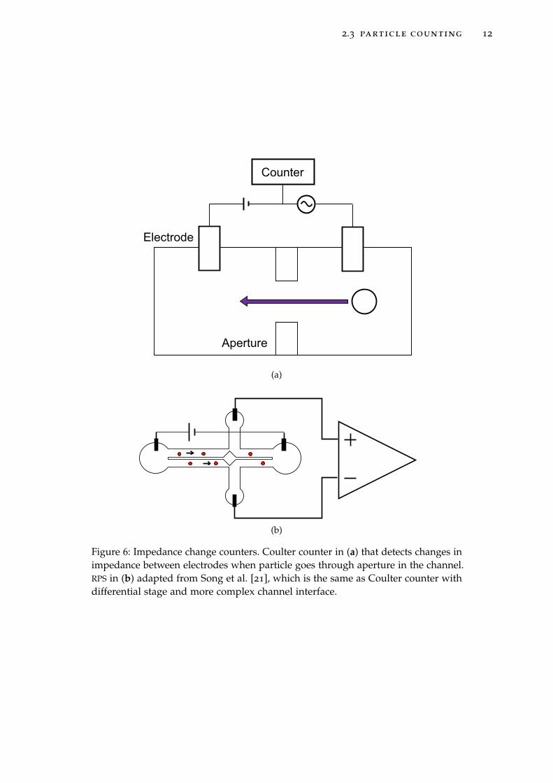
The most popular particle counting method is the Coulter Counter, where thereis a small aperture between two chambers and one electrode at each chamber(see Figure 6a). Once a particle goes through this aperture, the impedance of theconducting liquid and, therefore, between both electrodes, will increase dependingon the particle’s size. Currently, the available Coulter Counters can detect particlesranging from 0.4 to 1600 µm in size [19].

2.3 particle counting 11
Lightsource
Photodetector
Particle
(a)
Particle
Lightsource
Photodetector
(b)
200 um
(c)
Input fibre
Receivingfibre
Particle
Channel
MFD
MFD
(d)
Figure 5: Optical counters. Schematic in (a) and picture in (c) adapted from Schaferet al. [17] of a light-scattering counter, where the fibres form an angle with thechip’s channel. Light-blocking schematic in (b) and picture in (d) adapted fromXiang et al. [18], where both fibres are facing each other through the channel’sinterface.
This method of measuring the number of particles is also used in Resistive PulseSensors (RPS), able to detect particles in the nanometers scale [20]. As illustratedin Figure 6b, this detector is embedded into a microfluidic device, using two gatesconnected into a two-stage differential amplification system. Using this configura-tion, the noise is cancelled as one particle goes through one of the gates, subtractingthe noise floor from both inputs [21].
Another type of counter is the one that measures the change in capacitance ofthe fluid. The working principle is the same as the previous two, a particle goingthrough an aperture, but with the advantage of using low conducting fluids, unlikethe Coulter counter. As an example from Sohn et al. [22], this technique can beapplied to detect the DNA content in eukaryotic cells by creating a capacitancebridge of 1 kHz through the microfluidic device’s channel. This method needssome frequency modulation, increasing its complexity, and it may also produceelectric-field screening effects causing errors in the measurement.
2.3 particle counting 12
Counter
Electrode
Aperture
(a)
(b)
Figure 6: Impedance change counters. Coulter counter in (a) that detects changes inimpedance between electrodes when particle goes through aperture in the channel.RPS in (b) adapted from Song et al. [21], which is the same as Coulter counter withdifferential stage and more complex channel interface.

2.3 particle counting 13
2.3.3 Comparison
In Table 2, the main properties of the aforementioned counters are compared inorder to give a general overview of all devices. It can be observed those countersthat detect changes in impedance (Coulter and RPS) have the best sensitivity, butlack portability and the chip’s channel must be modified completely. In contrast,those counters based on light are less sensitive and do not need any change insidethe channel.
Table 2: Differences between counters. Different parameters of each particle counter,ordered from lower to higher sensitivity.
Sensitivity Complexity Cost Portability Change in channel
Coulter 0.40 µm High High Low YesRPS 0.09 µm Medium Medium Low YesCapacitance 10.00 µm Medium Low High YesLight-scattering 2.00 µm Low Low High NoLight-blocking 10.00 µm Low Low High No
As shown in Section 2.3, several detection methods can be used in this project.Table 2 compares all the properties of each one, making optical detectors the bestapproach in terms of portability and fewer changes in the chip. This property ispreferred for our setup as the main goal is adapting this detector into differentchips without changing their structure.
More specifically, according to this limitation, light-blocking detectors fit theproject’s needs. Light-reflecting ones have more complexity in aligning the emitterand detector at a certain angle without embedding them into the chip, as portrayedin Figure 5c.

14

3M E T H O D S
This Chapter explains the process of designing, creating and testing the opticaldetector adapted for Serial Crystallography in microfluidic devices.
3.1 resources
In order to achieve the main goal during this project, different tools were used andcan be divided into Software, Electronic equipment and Offline setup:
3.1.1 Software
1. SolidWorks: used to design 3D objects.
2. Altium Designer: used to create each Printed Circuit Board (PCB) design.
3. Orcad Capture: used to simulate circuits and estimate the right parameters.
4. Matlab: employed for post processing all data obtained from the oscilloscopeand creating graphs from it.
5. Affinity Designer: used to draw all diagrams with vector quality.
3.1.2 Electronic equipment
First of all, the following electronic equipment was used to monitor the circuits andto get images from the microscopic environment.
1. Oscilloscope (Siglent, model SDS1052DL+ 50 MHz): used to measure thereceivers’ output.
2. Power supply (PeakTech, model 6150): used to generate the 5V that powerseach PCB.
3. Signal generator (Siglent, model SDG1020 20 MHz): used to simulate crystalsin the interface between emitter and receiver.
4. Microscope (Ernst Leitz Wetzlar, model GMBH): used to visualize the crystalsand align the components.
5. Digital camera (ToupCam, UC3MOS): used to get images from the microscopementioned above.
Then, for creating each PCB, a Desktop Milling Machine (Roland, model SRM-20)was used. Afterwards, all the components were hand-soldered using a solder, tin,and flux to achieve a proper connection.
Finally, all structures were created using the following equipment:
15

3.1 resources 16
1. 3D printer (Prusa i3 MK3).
2. Laser Cutter (Trotec Speedy 400).
3. Stereolithography Apparatus (SLA) Printer. (Formlabs Form 3+).
3.1.3 Offline Setup
In order to carry out all the processes without using the Synchrotron’s beam-line,an offline setup simulating the beamline environment was assembled with thefollowing components: a microfluidic chip, a microlitre syringe, a set of samplesand complementary parts to hold them.
Microfluidic device and syringe
The microfluidic chip was connected to a Hamilton glass microlitre syringe anddifferent adapters, as depicted in Figure 7 with more detail in Figure 8. The chip(microfluidic chipshop, Fluidic 394), provided by the AdaptoCell group, has achannel height and width of 200 µm x 200 µm, respectively.
MICROFLUIDIC
DEVICE
MICROLITRE
SYRINGE
ADAPTERS
CONNECTING
TUBES
Figure 7: Microfluidic chip connected to a microlitre syringe.

3.1 resources 17
a b c d e f g h i j k
Figure 8: Syringe adapters. With the following components: (a) shows the Hamiltonsyringe; (b) a 100 µm ferrula; (c) the Hamilton needle with point style 3; (d) anIdex F-242X NanoTight Tubing Sleeve, Green FEP, 0.0155" ID x 1/16; (e - f) IdexNanoTight Fitting, Headless, Short, Natural PEEK/ETFE, Max 0.063" Hole, 1/16"OD Tubing; (g) Idex High-Pressure Union Body, True ZDV, PEEK, 0.010" ID, 1/16"OD Tubing; (h - i) Idex NanoTight Fitting, Headless, Short, Natural PEEK/ETFE,Max 0.063" Hole, 1/16" OD Tubing; (j) yellow tube, Idex F-246 NanoTight TubingSleeve, Yellow FEP, 0.027" ID x 1/16"; and (k) the connection tubes.
Imperfections
in Chip surface
Channel
(200 um)
Microcrystals
(a)
Imperfections
in Chip surface
Channel
(200 um)
Microcrystals
(b)
(c)
Figure 9: Measured samples, showing in (a) haemoglobin crystals inside the MFD’schannel, in (b) lysozyme crystals in the same channel and in (c) air bubbles throughthe buffer inside the microlitre syringe.

3.1 resources 18
Samples
As shown in Figure 9, the samples used for testing the detector correspond to crys-tals of haemoglobin and lysozyme mixed in a buffer solution with a relation of 1:7and 1:2, respectively, and a flow of air bubbles inside this buffer. The manufacturingmethod of the provided crystals, done by the AdaptoCell group, was the following:
• Haemoglobin: equine haemoglobin (Sigma, CAS-9047090) stock solutionof 20-25 mg/ml was prepared in 10 mM HEPES, pH 7.5 and precipitatedusing the stirred batch method2 by mixing into precipitant solution (26 % vPEG3350, 10mM HEMES pH 7.5). At 20 °C500 µl of precipitant were addedto 250 µl protein. The mixture was stirred in small HPLC vials with rice cornsized stir bars on a magnetic stirrer for about 20h.
• Lysozyme: chicken egg white Lysozyme from Alfa Aeser (J60701) was dis-solved at a concentration of 50 mg ml-1 in 100 mM Na Acetate pH 3.0. Ofthis lysozyme solution, 500 µl were mixed with 500 µl of precipitant, 19.04
% NaCl, 5.44 % PEG 8,000, 68mM Na Acetate pH 3.0 in an Eppendorf tubeand incubated overnight at 20 °C. Crystals grown in batch were spun downat room-temperature with 2,000 g for 1 min.
These crystals varied in size, with a surface area between 5 and 50 µm approxi-mately. As for the volumetric flow rate at the Synchrotron setup, it is constant andset to 10 nl/s.
Using Equation 1 and the values above, where Q is the flow rate and A thecross-sectional area, the crystals speed is equal to 250 µm/s.
v =Q
A[m/s] (1)

3.2 detection approach 19
3.2 detection approach
Assuming the crystals moved one at a time through the channel and with a separa-tion of 5 µm between each one, the approximate frequency of change was obtainedthrough Equation 2, where v and d correspond to the speed and minimum distancebetween changes (crystal going through the detector or not) respectively. Therefore,the setup should have a response frequency greater or equal to 50 Hz.
This distance was assumed and checked with the AdaptoCell group as a nonideal value in order to achieve a greater frequency than it was necessary, as thecrystals have larger gaps between them.
f =v
d[Hz] (2)
If we take into account that the optical detector has a sensing area of 0.23 mm2,the time of detection corresponds to 4,5 seconds approximately for each crystal.
3.2.1 Different setups
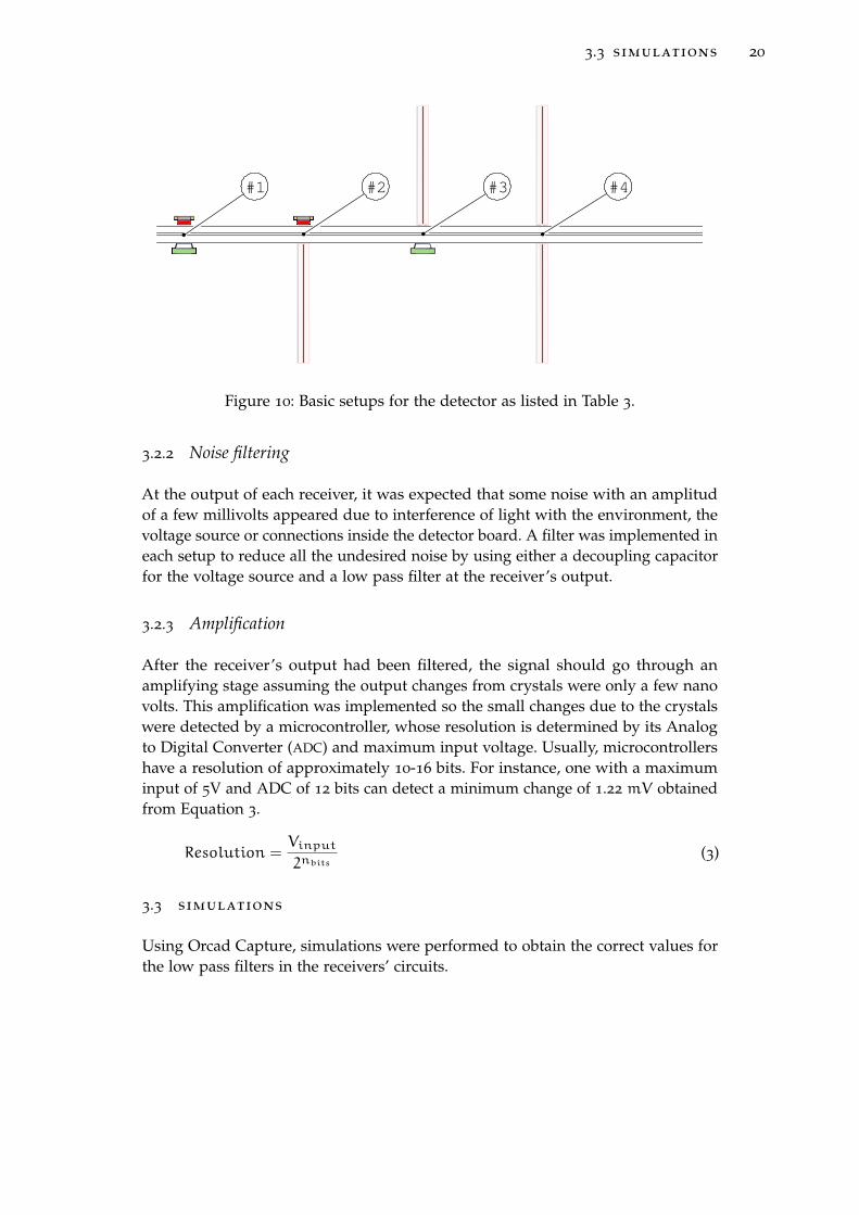
Once the type of detector had been decided, variations in the emitters and receiverswere used in order to obtain the best approach, giving place to different setups forthis project. Based on availability, low consumption and a size closer to the channel’swidth all emitters involved a Light Emitting Diode (LED). The receivers consistedof a Positive-Intrinsic-Negative (PIN) photodiode due to its small size and goodresponsivity to light. In addition, by using optical fibre adapters chosen to focus theemitted and received light, there are four main combinations listed in Table 3 andillustrated in Figure 10. Different LEDs, optical fibres and PIN diodes were used foreach setup. The resulting signal from this configuration would decrease its voltagewhenever a crystal or bubble goes through the detector due to light absorption ordiffraction, respectively.
Table 3: Different detector combinations for receiver and emitter.
Setup # Emitter Receiver
1 Plain LED Plain PIN diode2 Fibre Adapter with PIN diode
3 Fibre Adapter with LED Plain PIN diode4 Fibre Adapter with PIN diode
3.3 simulations 20
#2#1 #4#3
Figure 10: Basic setups for the detector as listed in Table 3.
3.2.2 Noise filtering
At the output of each receiver, it was expected that some noise with an amplitudof a few millivolts appeared due to interference of light with the environment, thevoltage source or connections inside the detector board. A filter was implemented ineach setup to reduce all the undesired noise by using either a decoupling capacitorfor the voltage source and a low pass filter at the receiver’s output.
3.2.3 Amplification
After the receiver’s output had been filtered, the signal should go through anamplifying stage assuming the output changes from crystals were only a few nanovolts. This amplification was implemented so the small changes due to the crystalswere detected by a microcontroller, whose resolution is determined by its Analogto Digital Converter (ADC) and maximum input voltage. Usually, microcontrollershave a resolution of approximately 10-16 bits. For instance, one with a maximuminput of 5V and ADC of 12 bits can detect a minimum change of 1.22 mV obtainedfrom Equation 3.
Resolution =Vinput
2nbits(3)
3.3 simulations
Using Orcad Capture, simulations were performed to obtain the correct values forthe low pass filters in the receivers’ circuits.

3.3 simulations 21
3.3.1 Low Pass Filter
The main goal of the Low-Pass filter (see Figure 11a) was to reduce the environ-mental noise while keeping the changes produced by the crystals. Therefore, aparametric sweep of the resistance was performed while keeping the capacitanceconstant (Figure 11b) based on three reasons: standardization of capacitor values,keeping a linear variation of the time constant (RC) and simplification the simula-tion. The best configuration with a 0.1 µF capacitor for keeping the original signalof the receiver with the least distortion was with R = 24 KΩ. Using Equation 4, thecut-off frequency was set at 66.32 Hz, as indicated at the simulation’s output.
As shown in Figure 11b, once the signal increased beyond the cut-off frequency,the gain was reduced drastically. Furthermore, as our noise source corresponded toa frequency of 10 KHz or higher (obtained from the oscilloscope), it can be observedin this graph that the signal at those frequencies has a gain close to zero.
fcutoff =1
2πRC(4)

3.3 simulations 22
5
5
4
4
3
3
2
2
1
1
D D
C C
B B
A A
Input Output
0
R1
24K
C1
0.1u
(a)
Fr equency
1. 0Hz 10Hz 100Hz 1. 0KHz 10KHz 100KHz 1. 0MHz. . . V(R1:2) / V(R1:1)
0
0. 2
0. 4
0. 6
0. 8
1. 0
(66. 325, 707. 047m)
(b)
Figure 11: Low pass filter simulation showing (a) the schematic circuit and (b) theresults from an AC parametric sweep where the cut-off frequency of the black lineis 66.325 Hz.

3.3 simulations 23
3.3.2 PIN with Fibre adapter Simulation
As shown in Figure 12, where the fibre adapter receiver was simulated, the ampli-fier’s input comprised three different voltage sources. A square signal representingthe receiver’s output with and without light (2 V and 1 V, respectively 1), a noisesource simulating the environmental noise at a frequency greater or equal than 5
kHz and 10mVpp as a non ideal value, and a smaller square signal characterizingthe receiver’s behaviour when a crystal goes through it (assuming 1 mV of ampli-tude and frequency of 50 Hz), decreasing the signal due to less light hitting thedetector.
Fibre Photodiode with noise
Light reductiondue to crystals
Power Supply
Low pass Filter
Fix gain Amplifier
Vcc
Vref
VSignal VSignal
Vref
Vcc
Filtered
Filtered
00
00
0
V
V
V
+
-
OUT
R1
C1
Vnoise
C2
PARAMETERS:
pot = 700
R4
Vphotodiode
R3
R2pot
Vmain5Vdc
R5Vcrystals
Figure 12: PIN receiver with fibre adapter simulated schematic, indicating thedifferent stages in the circuit.
Consequently, Figure 13 portrays different signals coming out of the circuitexplained above in a lapse of 20 ms. The first signal shows the receiver’s outputwithout filtering, being too difficult to tell the difference between noise and changesdue to the crystals. The second signal represents the low-pass filter’s output, beingdeformed due to the time constant t = RC and only with a change of 15 mV whena crystal goes through. Finally, the amplifier’s output is characterized by the lastsignal, showing perfectly when a change happens in the detector with a differenceof 800 mV without completely losing the signal due to the filtering stage.
1 Measured values with real components.

3.3 simulations 24
RAW SIGNAL:NO DETECTION
RAW SIGNAL:DETECTION
FILTERED:NO DETECTION
FILTERED:DETECTION
AMPLIFIED:NO DETECTION
AMPLIFIED:DETECTION
Figure 13: Receiver with fibre adapter simulation results, showing in (a) the re-ceiver’s output, in (b) the filtered signal and in (c) the amplified signal.
3.3.3 Plain PIN Simulation
Parallelly, another simulation was performed, including a model of the bare PIN
diode instead of the fibre adapter. As seen in Figure 14, the signal uses currentinstead of voltage sources due to the photodiode’s nature, generating current whenlight hits it. Similar to the previous simulation, two additional current sources wereincluded to mimic the noise and crystals effect into the receiver. The PIN diode wasconnected with its polarity inverted. Hence, when the photodiode increased itscurrent generation, the filter’s input voltage decreased and vice versa.
This signal goes through the low-pass filter and into the amplifying stage. In thispart, the signal was inverted using the negative port, and using the positive inputto set the output’s voltage level.
Once the values were set for a gain of 100 V/V , Figure 15 illustrates the differentoutputs through the circuit. Firstly, the direct receiver’s output shows almost nodifference between crystals and noise, filtered in Figure 15.b. After, the amplifier’ssignal in Figure 15.c makes it possible to differentiate whenever a crystal goesthrough with a variation of 70 mV instead of the 7 mV obtained at the input.

3.3 simulations 25
Plain Photodiode with noise
Low pass Filter
Light reductiondue to crystals
Power Supply
Fix gain Amplifier
ISignal Filtered
Vcc
Vref
Filtered
Vcc
Vref
ISignal
0
0
0 0
0
V
V
V
R2pot
+
-
4
OUT6
Inoise
R3
PARAMETERS:
pot = 580
C3
R1
C1
Icrystals
Iphotodiode
C2
R4
Vmain5Vdc
R5
Figure 14: Plain PIN receiver simulated schematic, indicating the different stages inthe circuit.

3.4 experimental 26
Figure 15: Receiver with plain PIN diode simulation results, showing in (a) thereceiver’s output, in (b) the filtered signal and in (c) the amplified signal.
3.4 experimental
3.4.1 Chosen components
All components used for the detector’s circuits are shown in Appendix A. Theoptical components (emitters, receivers and fibres) are listed in Table 4, where thepeak wavelength corresponds to a range between red and Infrared (IR) light. Thisrange was selected for two main reasons: the fibre adapters (used mainly for opticalcommunication) use only IR light and due to the colour of haemoglobin crystals.They are reddish and reflect more light inside this range of wavelengths [23], thusblocking more light going into the photodiode.
For choosing the ballast resistor, also known as the current limiting resistor,Equation 5 was used, being Vforward the voltage drop across the diode, Imax themaximum current for optimal performance, and Vcc the supply voltage, which was5 V for all circuits set by the voltage source.
R =Vcc− Vforward
Imax(5)
As explained in Section 3.2, the receiver setup must be able to have a frequencyresponse greater or equal than 50 Hz, which was fulfilled by all components.
For the amplifying stage, two different amplifiers were used for each receiver:one with adjustable gain (MAX4460ESA+ ), and another with a fixed gain of 10

3.4 experimental 27
Table 4: List of optical components with the main properties of each one.
Name Wavelength Vf Current [mA] Extra
0603 IR LED 850 nm 1.4 V 20mA -0603 Red LED 650 nm 2.0 V 20mA -IFE98 (emitter) 650 nm 1.9 V 20 mA Jacket = 2.2 mmHFBR-1414TZ (emitter) 820 nm 1.9 V 80 mA Jacket = 1 mmHFBR 2416TZ (receiver) 820 nm - 25 mA -OPF522 (receiver) 850 nm - 25 mA -SFH 2716 PIN 620 nm - 0.6 µA Area = 1 mm2
VEMD1060X01 PIN 820 nm - 1.8 µA Area = 0.23 mm2
Optic Fibre 62.5/125 - - - Rmin= 1.8 mmOptic Fibre 980/1000 - - - Rmin= 25 mm
V/V (MAX4461TESA+). These amplifiers provided an output following Equation 6,connecting V+ to the filtered signal of the receiver and V− to the reference voltageused to avoid saturation in the output at a certain gain.
Vout = Gain · (V+ − V−) (6)
Gain = 1+R2
R1(7)
Potentiometers had been chosen for three main applications: increasing theemitters’ ballast resistance to decrease the light intensity, acting as a voltage dividerin the reference voltage of the amplifiers and adjusting the amplifier’s gain asdescribed by Equation 7.
Both receivers with fibre adapters have internal amplifying stages. The HFBR2416TZ receiver has a low noise transimpedance preamplifier, whereas the OPF22
receiver has an open collector output transistor, leading to a decrease in voltagewhen light is received.
3.4.2 Final arrangement
Consequently, the final detector’s layout consisted on a combination of PCBs, wires,electronic equipment and structures to hold all components in position.
3.4.2.1 Boards
In order to reduce the quantity of PCBs designs and keep only the essential compo-nents attached to the chip, three different boards were created containing all neededcomponents:

3.4 experimental 28
• Board 001 (see Figure 16):
This circuit has three main parts. First of all, the emitters region, containingboth LED fibre emitters and a connector for the external Surface MountedDevice (SMD) LEDs (Board 003). With their calculated ballast resistors, thisboard includes a potentiometer that allows variation in light brightness bychanging the total resistance. An SP3T switch powers the desired emitter.
Another main part consists of the receivers. Within this region, two photodi-odes with fibre adapters can be found along with a connector for an externalreceiver (Board 002). Similarly to the aforementioned region, the user canpower each receiver with another SP3T switch. A filtering and amplifyingstage are included to improve the fibre receivers’ signal. Instead of using twoidentical sets of components, a third switch redirects the desired receiver’ssignal. In this amplifying stage, both the reference voltage and the gain canbe adjusted either by a fixed pair of resistors or by the potentiometers. Extracomponents footprints are added depending on the used amplifier.
A third region contains the power ports and test points for the receivers’signals.
• Board 002(see Figure 17):
This board contains the plain photodiode with its filtering and amplifyingstage with the same variations as explained in Board 001.
• Board 003(see Figure 18):
The plain LEDs only needs a ballast resistor in their circuit in order to work.There are two boards of this type, one for each LED, which are connected toBoard 001.

3.4 experimental 29
1
1
2
2
3
3
4
4
D D
C C
B B
A A
BRD001
1 1
BRD001
BRD001 1.015/05/2022 17:12:59
Title:
Size: Number:Date:
Revision:Sheet ofTime:
A4
Drawn By: Carlos&Jaime -Checked By:
Page Contents: 01-Schematic.SchDoc
SOLDEREDVariant:
1 1
J1
5004
1 1
J3
5004
GND
Vcc
NC1
Anode2
Cathode3
NC4 NC 5Anode 6Anode 7NC 8J2
HFBR-1414TZ
NC1
Signal2
V_EE3
NC4 NC 5Vcc 6V_EE 7NC 8J8
HFBR-2416TZ
1234
D1
IF-E98
100K
VR1PT01-D115D-B104
CBA
SW1
OS103011MS8QP1
CBA
SW2
OS103011MS8QP1
21
34
J5
PH1RA-04-UA
1
2
1
2
J4
CMP-15831-000009-1
Vcc
R1
43
R2
160
GND
GND
Vcc
OutVcc
GND
D2
OPF522GND GND
GND
GND
OutA
GND
1 1
J6
5004
OutA 1 1
J7
5004
OutFibre
OutB
GND
OutC
OutB
12
0.1uF
C1R324K
GND
FilteredRaw
Noise Filter
Vref
R4680
R5270
GND
Vcc
Amp. Reference
Vref
12
0.1uFC3
GND
Filtered
GND
Pin8
Amplifier
12
0.1uFC2
GND
Vcc
OutFibre
R70
R8100
R91
GND
R6
0Vcc
Gain Adjustment
Place this Resistor if MAX4460
Place this Resistor if MAX4461
Pin8
OutFibre
Receivers
IN+3
IN-6
FB8
NC4
NC5
VDD 7
OUT 1
GND 2
U1
MAX4460ESA+
Raw
100KVR3
20KVR2
OutC
CBA
SW3
OS103011MS8QP1
R10560
Raw output Selector
Power ports
Final output ports
Emitters
The sum of resistors (R1 + R2) near 100kΩ is a good compromise
The MAX4460 gain is set by connecting a resistivedivider from OUT to GND, with the center tap connected to FB (Figure 2). The gain is calculated by:Gain = 1 + R8 / R9
PIC101 PIC102
COC1
PIC201 PIC202
COC2
PIC301 PIC302
COC3
PID10A
PID10K
COD1
PID20GND
PID20VCC
PID20VOUT
COD2
PIJ101
COJ1
PIJ201
PIJ202
PIJ203
PIJ204 PIJ205
PIJ206
PIJ207
PIJ208
COJ2
PIJ301
COJ3
PIJ401
PIJ402
COJ4
PIJ501
PIJ502
PIJ503
PIJ504
COJ5
PIJ601
COJ6
PIJ701
COJ7
PIJ801
PIJ802
PIJ803
PIJ804 PIJ805
PIJ806
PIJ807
PIJ808
COJ8
PIR101 PIR102
COR1
PIR201 PIR202
COR2
PIR301 PIR302
COR3
PIR401
PIR402 COR4
PIR501
PIR502
COR5
PIR601 PIR602
COR6
PIR701
PIR702
COR7
PIR801
PIR802
COR8
PIR901
PIR902
COR9
PIR1001
PIR1002
COR10
PISW101
PISW102 PISW103
PISW104
COSW1
PISW201
PISW202 PISW203
PISW204
COSW2
PISW301
PISW302 PISW303
PISW304
COSW3
PIU101
PIU102
PIU103
PIU104
PIU105
PIU106
PIU107
PIU108
COU1
PIU101
PIU107
PIVR101
PIVR102
PIVR103 COVR1
PIVR201
PIVR202
PIVR203 COVR2
PIVR301
PIVR302
PIVR303 COVR3
PIC101 PIR302
PIU103 NLFiltered
PIC102
PIC202
PIC302
PID10K
PID20GND
PIJ203
PIJ301 PIJ401
PIJ502
PIJ504
PIJ803
PIJ807
PIR502
PIR902
PIU102
PIVR201
PIVR301
NLGND
PID10A
PIR201
PID20VCC
PIR1001
PISW203
PIJ201
PIJ202
PIJ206
PIJ207 PIR101
PIJ204 PIJ205
PIJ208
PIJ402
PISW101
PIJ501
PISW201
PIJ801
PIJ804 PIJ805
PIJ806
PISW204
PIJ808
PIR102
PISW104
PIR202 PISW103
PIR702
PIR802 PIR901
PIVR302
PISW102
PIVR103
PISW303
PIU104
PIU105
PIVR101
PIJ503
PIJ601 NLOutA
PID20VOUT PIR1002
PISW304 NLOutB
PIJ802
PISW301 NLOutC
PIJ701
PIR801
PIU101
PIVR303
NLOutFibre
PIR601
PIR701
PIU108
NLPin8
PIR301
PISW302 NLRaw
PIC201
PIJ101
PIR402
PIR602
PISW202
PIU107
PIVR102
PIVR203
NLVcc
PIC301
PIR401 PIR501
PIU106
PIVR202
NLVref
Figure 16: Board 001 generated with Altium Designer.

3.4 experimental 30
1
1
2
2
3
3
4
4
D D
C C
B B
A A
BRD002
1 1
BRD002
BRD002 1.015/05/2022 17:15:36
Title:
Size: Number:Date:
Revision:Sheet ofTime:
A4
Drawn By: Carlos&Jaime -Checked By:
Page Contents: 01-Schematic.SchDoc
Adjt. Amp: Adjt. Gain - Adjt. ReferenceVariant:
IN+3
IN-6
FB8
NC4
NC5
VDD 7
OUT 1
GND 2
U1
MAX4460ESA+
A K
D1
SFH 2716GND
Raw
Vref
R2680
R3270
GND
Vcc
12
0.1uF
C1R124K
GND
FilteredRaw
20K
VR13203X203P
12
0.1uFC3
GND
R50
R699
R71
GND
GND
R4
0Vcc
Light detector Noise Filter
Amp. Reference
Gain Adjustment
Pin8
Place this Resistor if MAX4460
Place this Resistor if MAX4461
Amplifier
12
0.1uFC2
GND
Vcc
100K
VR23203X104P
Pin8
Out
Out
Out
VccGND 2
1
34
J1
PH1RA-04-UA
GND
VrefFiltered
R8
280
R9
280
1 2
0.1uF
C4
Connector
The sum of resistors (R1 + R2) near 100kΩ is a good compromise
Right- less GainTotalR: 110K
The MAX4460 gain is set by connecting a resistivedivider from OUT to GND, with the center tap connected to FB (Figure 2). The gain is calculated by:Gain = 1 + R2 / R1
PIC101 PIC102
COC1
PIC201
PIC202 COC2
PIC301 PIC302
COC3
PIC401 PIC402
COC4
PID10A PID10K
COD1
PIJ101
PIJ102
PIJ103
PIJ104
COJ1
PIR101 PIR102 COR1
PIR201
PIR202 COR2
PIR301
PIR302
COR3
PIR401 PIR402
COR4
PIR501
PIR502
COR5
PIR601
PIR602
COR6
PIR701
PIR702
COR7
PIR801 PIR802
COR8 PIR901 PIR902
COR9
PIU101
PIU102
PIU103
PIU104
PIU105
PIU106
PIU107
PIU108
COU1
PIU101
PIU107
PIU101
PIU107
PIVR101
PIVR102
PIVR103 COVR1
PIVR201
PIVR202
PIVR203 COVR2
PIC101
PIC401
PIR102
PIR801
PIU106 NLFiltered
PIC102
PIC202
PIC302
PID10A
PIJ102
PIJ104
PIR302
PIR702
PIU102
PIVR101
PIVR201
NLGND
PIR502
PIR602 PIR701 PIVR202
PIR802 PIR901
PIU101
PIU104
PIU105
PIU107
PIC402
PIJ103
PIR601
PIR902
PIU101
PIVR203
NLOut
PIR401
PIR501
PIU108
NLPin8
PID10K
PIR101 NLRaw
PIC201
PIJ101
PIR202
PIR402
PIU107
PIVR103
NLVcc
PIC301 PIR201 PIR301
PIU103
PIVR102 NLVref
Figure 17: Board 002 generated with Altium Designer.

3.4 experimental 31
1
1
2
2
3
3
4
4
D D
C C
B B
A A
BRD003
1 1
BRD003
BRD003 1.015/05/2022 17:18:35
Title:
Size: Number:Date:
Revision:Sheet ofTime:
A4
Drawn By: Carlos & Jaime -Checked By:
Page Contents: 01-Schematic.SchDoc
[No Variations]Variant:
12
12
J1
CMP-15831-000009-1
1 2
D1
R1GND
LED with ballast resistor
PID101 PID102
COD1
PIJ101 PIJ102
COJ1
PIR101
PIR102
COR1
PID102
PIJ101
PID101
PIR102
PIJ102
PIR101
Figure 18: Board 003 generated with Altium Designer.

3.4 experimental 32
Combining these three boards, the main four setups from Table 3 can be expandedinto further combinations listed in Table 5.
Table 5: Setups with chosen components where each emitter is tested with fourreceivers
Setup # Emitter Receiver
1.1.1 0603 IR LED SFH 2716 PIN
1.1.2 VEMD1060X01 PIN
1.2.1 0603 Red LED SFH 2716 PIN
1.2.2 VEMD1060X01 PIN
2.1.1 0603 IR LED HFBR 2416TZ receiver2.1.2 OPF522 receiver
2.2.1 0603 Red LED HFBR 2416TZ receiver2.2.2 OPF522 receiver
3.1.1 IFE98 RED SFH 2716 PIN
3.1.2 VEMD1060X01 PIN
3.2.1 HFBR-1414TZ IR SFH 2716 PIN
3.2.2 VEMD1060X01 PIN
4.1.1 IFE98 RED HFBR 2416TZ receiver4.1.2 OPF522 receiver
4.2.1 HFBR-1414TZ IR HFBR 2416TZ receiver4.2.2 OPF522 receiver

3.4 experimental 33
3.4.2.2 Mechanical design
In order to hold all components in place, different structures were designed asexplained below, illustrated together in Figure 19.
c
k
f
a
b
g
h
i
j
e
d
Figure 19: Offline setup with detector. Showing in (a) the syringe pump, in (b) theflow control knob, in (c) the stand, in (d) the control panel, in (e) the power testclamps, in (f) the output’s test points, in (g) the eppendorf tubes and holder, in (h)the optical interface in the chip, in (i) the chip holder from the AdaptoCell group,in (j) a magnet holder and in (l) the microlitre syringe.
syringe pump :Concerning the constant flow of crystals into the microfluidic chip, using themicrolitre syringe with bare hands was not steady enough. A low-cost manualpump was designed for this purpose. As shown in Figure 20, this pump consistedof four main parts:
• Syringe press: pushes the plunger and keeps the syringe in place, resulting inconverting circular to linear motion.
• Gear train: reduces the movement speed by a factor of 14.

3.4 experimental 34
aj
g
e
f
h
i
k
l
c
b
d
Figure 20: Syringe pump exploded view. Indicated in (a) the structure’s lateral wallswith axis holes, in (b) the syringe press with rack, in (c) the structure’s sides, in(d) the control knob, in (e) the structure’s bottom, in (f) the driving gear, in (g) thedriven gear, in (h-i) the gear axis with shaft key, in (j) the structure’s corners, in (k)the structure’s top and in (l) the syringe holder.
• Control knob: moves the gear train to one side or the other using the handonly.
control panel :To protect and improve the handling of Board 001, a plastic enclosure (Figure 19.d)was designed along with adapters for the sliders and the brightness potentiometer.It allowed access to the power and output signal ports and the other potentiometers.
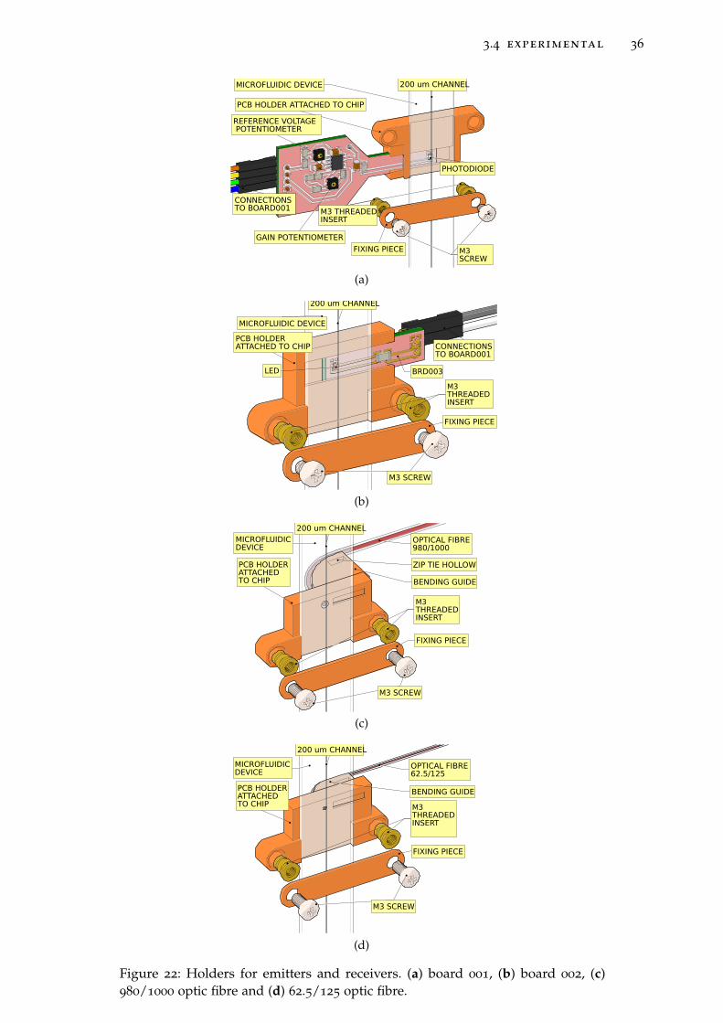
emitter and receiver holders :In order to achieve the best transference of light from the emitter to the receiver, itwas essential to align both components. Other losses could appear in the opticalfibres’ case, as depicted in Figure 21. Different parts were designed to reach thisalignment and hold the components in place, as represented in Figure 22.

3.4 experimental 35
Figure 21: Possible causes for mismatch in fibre-to-fibre connections [24].
3.4 experimental 36
M3 THREADEDINSERT
FIXING PIECE
PHOTODIODE
M3SCREW
200 um CHANNEL
GAIN POTENTIOMETER
PCB HOLDER ATTACHED TO CHIP
MICROFLUIDIC DEVICE
REFERENCE VOLTAGE POTENTIOMETER
CONNECTIONS TO BOARD001
(a)
CONNECTIONSTO BOARD001
BRD003
FIXING PIECE
LED
M3 THREADED INSERT
PCB HOLDERATTACHED TO CHIP
M3 SCREW
200 um CHANNEL
MICROFLUIDIC DEVICE
(b)
OPTICAL FIBRE980/1000
BENDING GUIDE
FIXING PIECE
M3THREADEDINSERT
M3 SCREW
PCB HOLDERATTACHEDTO CHIP
ZIP TIE HOLLOW
200 um CHANNELMICROFLUIDICDEVICE
(c)
OPTICAL FIBRE62.5/125
FIXING PIECE
M3 THREADEDINSERT
M3 SCREW
PCB HOLDERATTACHEDTO CHIP
BENDING GUIDE
200 um CHANNEL
MICROFLUIDICDEVICE
(d)
Figure 22: Holders for emitters and receivers. (a) board 001, (b) board 002, (c)980/1000 optic fibre and (d) 62.5/125 optic fibre.

3.4 experimental 37
stand :As depicted in Figure 19, this structure had the purpose of holding the syringepump on the top and the microfluidic chip in a vertical position attached to amagnet, simulating the real setup at the beamline.

38

4R E S U LT S
In this Chapter, two types of results are explained. First of all, the entire processof PCB manufacturing is shown, as well as the result of each mechanical piece thatwas designed. Afterwards, all obtained results from the oscilloscope are plottedinto different grouped graphs.
4.1 mechanical results
4.1.1 PCBs
Two sets of PCBs were created using the Desktop SRM-20 Milling machine: the testboards and the final boards.
Tests boards
During the entire process of testing each component, several boards were designedbefore reaching the final design, fixing errors by using wires when needed (seeFigure 23).
For the emitting circuits, only two pins were connected to each one, testing themwith the proper resistor in a protoboard. In addition, all receivers were tested usinga fixed gain amplifier but no filtering stage, leading to a noisy output.
(a) (b) (c) (d) (e) (f)
Figure 23: Test boards for different components. (a) and (b) correspond to both LEDs,(c) is the PIN photodiode with amplifier, (d) is the PCB for two emitters with adapterfor fibre of 980 µm core, (e) is a PIN receiver with fibre adapter and amplifier, and(f) is another emitter with adapter for fibre with 62.5 µm core.
39
4.1 mechanical results 40
Final boards
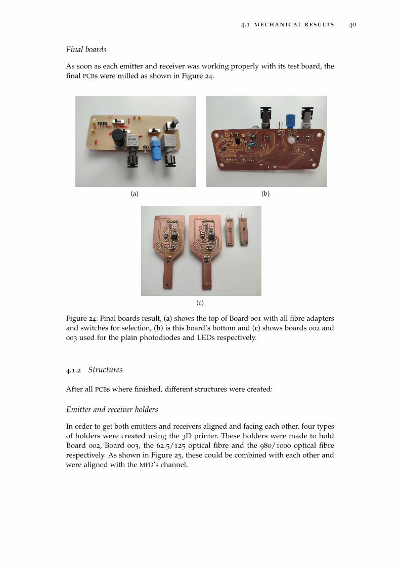
As soon as each emitter and receiver was working properly with its test board, thefinal PCBs were milled as shown in Figure 24.
(a) (b)
(c)
Figure 24: Final boards result, (a) shows the top of Board 001 with all fibre adaptersand switches for selection, (b) is this board’s bottom and (c) shows boards 002 and003 used for the plain photodiodes and LEDs respectively.
4.1.2 Structures
After all PCBs where finished, different structures were created:
Emitter and receiver holders
In order to get both emitters and receivers aligned and facing each other, four typesof holders were created using the 3D printer. These holders were made to holdBoard 002, Board 003, the 62.5/125 optical fibre and the 980/1000 optical fibrerespectively. As shown in Figure 25, these could be combined with each other andwere aligned with the MFD’s channel.

4.1 mechanical results 41
(a) (b) (c)
(d) (e) (f)
Figure 25: Emitter and receiver holders combinations. Board 002 aligned with(a) Board 003, (b) 62.5/125 optical fibre and (c) 980/1000 optical fibre. Next, the62.5/125 optical fibre aligned with (d) Board 003, (e) 62.5/125 optical fibre and (f)980/1000 optical fibre.

4.2 data from different setups 42
Syringe pump
As mentioned in Section 3.4.2.2, moving the microlitre syringe with the bare handswas not steady enough. So the syringe pump was created as illustrated in Figure 26.This structure was assembled and appropriately worked using the 3D printer forthe gears’ axis and corners, and the Laser cutter for the remaining parts.
Control panel
Connected to Board 002 and 003 in Figure 26, Board 001 was enclosed insidea control box created with the 3D printer. This box was designed to control allactuators on the board, such as the brightness potentiometer and SP3T switches.To better interact with the user, this box was printed using two different colours toshow the switch positions and all necessary connections.
Stand
The white stand shown in Figure 26 was manufactured in acrylic plastic using theLaser Cutter and had a 3D printed magnet holder at the end of it. This structurewas able to hold the syringe pump and the MFD without failures.
Figure 26: Complete assembly.
4.2 data from different setups
In this Section, several graphs obtained with the oscilloscope are depicted and postprocessed using the Matlab script shown in Appendix C. There are four differentmeasurements in the receiver’s output for each sub setup listed in Table 5: responseto input light and no light, air bubbles inside the buffer, haemoglobin crystals, andlysozyme crystals. Each time a measurement was performed, the MFD was attached

4.2 data from different setups 43
to the optical detector as well as to the microscope in order to check if the bubblesor crystals were going through the channel. Between each measurement, ethanolwas introduced into the syringe and the device in order to dissolve the crystals thatremained inside. Bubbles were injected manually taking air with the micropipettes.
All measurements were performed under low and constant light in the envi-ronment so the changes in the detector were not affected by it. In addition, allpotentiometers were adjusted to obtain the highest gain for the lowest changeswithout saturating the output following the procedure illustrated in Figure 27.Except those showing the light response, all graphs include an additional signal.This signal corresponds to calculating the moving average of the oscilloscope’soutput every 100 points, which corresponds to 10 ms, to get a clear view of thechanges without the noise floor. This process has the drawback of missing part ofthe signal, but given the low flow rate of the fluid it was not a critical issue.
AdjustReferencepotentiometeroutput voltage
AdjustGainpotentiometer
Fibreadapter
?
saturatedoutput
?
Closer to 0
Reduce gainYES
YES
NO
NO
Closer toreceiver‘s output
Increase gain
Turn on light sourcefor max. signal
Figure 27: Calibration procedure for amplifying stage.
Last but not least, the light intensity played an essential role in the detection. Atmaximum brightness, the receivers could not detect any changes due to the amountof light coming through the channel, from its surroundings and reflections. Thebrightness potentiometer was adjusted for each setup to achieve better results.
4.2.1 Alignment
The alignment was performed in two steps. First of all, the emitter was aligned intothe chip’s channel using the microscope. Then, the second step involved the LED
positioning by looking at the receiver’s output. Once the signal reached its peak,that meant emitter and receiver were aligned. As an additional check, the lightchanging graphs were a method to prove an optimal optical connection. As shown

4.2 data from different setups 44
in Figure 28, each emitter was centred into the channel in a similar way, allowingthe light to be focused.
(a) (b) (c)
(d) (e)
Figure 28: Emitters and receivers alignment with the MFD’s channel. In (a-b) itshows both plain photodiodes, whereas in (c) there is the IR LED and in (d-e) bothtypes of fibre.

4.2 data from different setups 45
4.2.2 Crystals measurements
As shown in Figure 29, no configuration was able to detect changes in the signalwhen a crystal went through.
0 2 4 6 8 10 12 14 16 18 20
Time [s]
4.6
4.65
4.7
4.75
4.8
4.85
4.9
Voltage [V
]
Oscilloscope
Mean value
(a)
0 2 4 6 8 10 12 14 16 18 20
Time [s]
4.6
4.65
4.7
4.75
4.8
4.85
4.9
Voltage [V
]
Oscilloscope
Mean value
(b)
Figure 29: Haemoglobin and Lysozyme crystals measurements from all setupsgiving no distinguishable changes.

4.2 data from different setups 46
4.2.3 Setup 1: Plain LED and plain PIN diode
This configuration consisted of a plain photodiode facing a plain LED and therewere four different configurations used:
0603 IR LED and SFH 2716 PIN (1.1.1)
• Light difference: 1.72 V
• Bubbles difference: 55.44 mV
• Percentage: 3.22 %
0 2 4 6 8 10 12 14 16 18 20
Time [s]
1.5
2
2.5
3
3.5
4
4.5
Volta
ge [V
]
OscilloscopeX 4.91
Y 3.96
X 14.193
Y 2.24
(a)
0 2 4 6 8 10 12 14 16 18 20
Time [s]
3.8
3.85
3.9
3.95
4
4.05
4.1
Volta
ge [V
]
Oscilloscope
Mean value
X 9.955
Y 3.97584
X 11.98
Y 3.9204
(b)
Figure 30: Setup 1.1.1 measurements, showing in (a) the response due to switchingON/OFF the light source and in (b) small changes when an air bubble goes through.

4.2 data from different setups 47
0603 IR LED and VEMD1060X01 PIN (1.1.2)
• Light difference: 0.9 V
• Bubbles difference: 48 mV
• Percentage: 5.3 %
0 2 4 6 8 10 12 14 16 18
Time [s]
1.5
2
2.5
3
3.5
4
Vo
ltag
e [
V]
Oscilloscope
X 12.885
Y 3.42
X 16.843
Y 2.52
(a)
0 2 4 6 8 10 12 14 16 18 20
Time [s]
3.2
3.25
3.3
3.35
3.4
3.45
3.5
Vo
ltag
e [
V]
Oscilloscope
Mean value
X 13.343
Y 3.38
X 17.644
Y 3.332
(b)
Figure 31: Setup 1.1.2 measurements, showing in (a) the response due to switchingON/OFF the light source and in (b) small changes when an air bubble goesthrough..

4.2 data from different setups 48
0603 RED LED and SFH 2716 PIN (1.2.1)
• Light difference: 1.22 V
• Bubbles difference: 40 mV
• Percentage: 3.28 %
0 2 4 6 8 10 12 14 16 18 20
Time [s]
1.5
2
2.5
3
3.5
4
4.5
Vo
ltag
e [
V]
Oscilloscope
X 5.04
Y 3.28
X 15.718
Y 2.06
(a)
0 2 4 6 8 10 12 14 16 18 20
Time [s]
3.2
3.25
3.3
3.35
3.4
3.45
3.5
Vo
ltag
e [
V]
Oscilloscope
Mean value
X 12.673
Y 3.336
X 15.877
Y 3.296
(b)
Figure 32: Setup 1.2.1 measurements, showing in (a) the response due to switchingON/OFF the light source and in (b) small changes when an air bubble goes through.

4.2 data from different setups 49
0603 RED LED and VEMD1060X01 PIN (1.2.2)
• Light difference: 0.64 V
• Bubbles difference: 41.8 mV
• Percentage: 6.53 %
0 2 4 6 8 10 12 14 16 18 20
Time [s]
1.5
2
2.5
3
3.5
4
4.5
Vo
ltag
e [
V]
Oscilloscope
X 12.322
Y 2.66
X 17.823
Y 2.02
(a)
0 2 4 6 8 10 12 14 16 18 20
Time [s]
2.5
2.55
2.6
2.65
2.7
2.75
2.8
Vo
ltag
e [
V]
Oscilloscope
Mean value
X 11.459
Y 2.649
X 13.598
Y 2.6072
(b)
Figure 33: Setup 1.2.2 measurements, showing in (a) the response due to switchingON/OFF the light source and in (b) small changes when an air bubble goesthrough..

4.2 data from different setups 50
4.2.4 Setup 2: Plain LED and PIN diode with fibre adapter
For this setup, in Figure 34 no noticeable changes can be observed due to the lightswitching. Therefore, further measurements were not taken.
0 2 4 6 8 10 12 14 16 18 20
Time [s]
0.5
1
1.5
2
2.5
3
3.5
4
4.5
5
5.5
Vo
lta
ge
[V
]
(a)
0 2 4 6 8 10 12 14 16 18 20
Time [s]
0.5
1
1.5
2
2.5
3
3.5
4
4.5
5
5.5
Vo
ltag
e [
V]
(b)
Figure 34: Setup 2 measurements, showing the lack of response due to switchingON/OFF the light source in Sub-setups (a) 2.1.1, (b) 2.1.2, (c) 2.2.1 and (d) 2.2.2.

4.2 data from different setups 51
4.2.5 Setup 3: LED with fibre adapter and plain PIN diode
This configuration consisted of an optical fibre facing a plain PIN photodiode andthere were four different configurations used:
IFE98 RED and SFH 2716 PIN (3.1.1)
• Light difference: 1.76 V
• Bubbles difference: 76.56 mV
• Percentage: 4.35%
0 2 4 6 8 10 12 14 16 18 20
Time [s]
1.5
2
2.5
3
3.5
4
4.5
Voltage [V
]
OscilloscopeX 9.497
Y 4.08
X 15.276
Y 2.32
(a)
0 2 4 6 8 10 12 14 16 18 20
Time [s]
3.8
3.85
3.9
3.95
4
4.05
4.1
Voltage [V
]
Oscilloscope
Mean value
X 12.006
Y 4.02272
X 14.028
Y 3.94616
(b)
Figure 35: Setup 3.1.1 measurements, showing in (a) the response due to switchingON/OFF the light source and in (b) small changes when an air bubble goes through.

4.2 data from different setups 52
IFE98 RED and VEMD1060X01 PIN (3.1.2)
• Light difference: 0.32 V
• Bubbles difference: 42.4 mV
• Percentage: 13.25 %
0 2 4 6 8 10 12 14 16 18 20
Time [s]
1.5
2
2.5
3
3.5
4
4.5
Vo
lta
ge
[V
]
Oscilloscope
X 9.612
Y 2.54
X 12.452
Y 2.22
(a)
0 2 4 6 8 10 12 14 16 18 20
Time [s]
2.4
2.45
2.5
2.55
2.6
2.65
2.7
Vo
lta
ge
[V
]
Oscilloscope
Mean value
X 13.338
Y 2.5482
X 15.042
Y 2.5058
(b)
Figure 36: Setup 3.1.2 measurements, showing in (a) the response due to switchingON/OFF the light source and in (b) small changes when an air bubble goes through.

4.2 data from different setups 53
HFBR-1414TZ IR and SFH 2716 PIN (3.2.1)
• Light difference: 0.96 V
• Bubbles difference: 87.28 mV
• Percentage: 9.09 %
0 2 4 6 8 10 12 14 16 18 20
Time [s]
1.5
2
2.5
3
3.5
4
4.5
Vo
lta
ge
[V
]
Oscilloscope
X 12.42
Y 3.6
X 10.242
Y 2.64
(a)
0 2 4 6 8 10 12 14 16 18 20
Time [s]
3.25
3.3
3.35
3.4
3.45
3.5
3.55
Vo
lta
ge
[V
]
Oscilloscope
Mean value
X 14.612
Y 3.46008
X 18.608
Y 3.3728
(b)
Figure 37: Setup 3.2.1 measurements, showing in (a) the response due to switchingON/OFF the light source and in (b) small changes when an air bubble goes through.

4.2 data from different setups 54
HFBR-1414TZ IR and VEMD1060X01 PIN (3.2.2)
• Light diff: 0.64 V
• Bubbles diff: 19.92 mV
• Percentage: 3.11 %
0 2 4 6 8 10 12 14 16 18 20
Time [s]
1.5
2
2.5
3
3.5
4
4.5
Vo
ltag
e [
V]
Oscilloscope
X 12.322
Y 2.66
X 17.823
Y 2.02
(a)
0 2 4 6 8 10 12 14 16 18 20
Time [s]
1.9
1.95
2
2.05
2.1
2.15
2.2
Vo
lta
ge
[V
]
Oscilloscope
Mean value
X 14.606
Y 2.07384
X 16.259
Y 2.05392
(b)
Figure 38: Setup 3.2.2 measurements, showing in (a) the response due to switchingON/OFF the light source and (b) small changes when an air bubble goes through.

4.2 data from different setups 55
4.2.6 Setup 4: LED and PIN diode with fibre adapter
In this Setup, the signal generated by switching the emitters and changing theirlight intensity was non-variable. Therefore, no more tests were performed with thesamples because no light was detected at the receiver.
0 2 4 6 8 10 12 14 16 18 20
Time [s]
0.5
1
1.5
2
2.5
3
3.5
4
4.5
5
5.5
Vo
lta
ge
[V
]
(a)
0 2 4 6 8 10 12 14 16 18 20
Time [s]
0.5
1
1.5
2
2.5
3
3.5
4
4.5
5
5.5
Vo
lta
ge
[V
]
(b)
0 2 4 6 8 10 12 14 16 18 20
Time [s]
0.5
1
1.5
2
2.5
3
3.5
4
4.5
5
5.5
Vo
lta
ge
[V
]
(c)
0 2 4 6 8 10 12 14 16 18 20
Time [s]
0.5
1
1.5
2
2.5
3
3.5
4
4.5
5
5.5
Vo
lta
ge
[V
]
(d)
Figure 39: Setup 4 measurements, showing the lack of response due to switchingON/OFF the light source in Sub-setups (a) 4.1.1, (b) 4.1.2, (c) 4.2.1 and (d) 4.2.2.

4.3 direct connections 56
4.3 direct connections
Taking into account the negative outcome from those setups containing fibre re-ceivers, two different methods were performed in order to achieve a better alignmentbetween these fibres. On the one hand, the connector shown in Figure 40a wasmade using the SLA printer due to its vertical resolution of 25 µm, where bothfibres are inserted in between. On the other hand, using the Laser Cutter a hole wascreated in an acrylic piece as shown in Figure 40c. These two attempts of aligningthe fibres gave similar outcomes as those in Figure 34 and 39.
(a) (b)
(c) (d)
Figure 40: Optical fibres alignment, using (a-b) an SLA printed connector and (c-d)a laser-cut hole.
Another attempt for connecting both fibre emitters and receivers was done. Asseen in Figure 41, the optical fibres are connected directly from one end to the otherwithout any cuts or chip in the middle. It can be observed that the receivers’ signalsare working, showing a square signal due to the emitter switching ON/OFF.

4.3 direct connections 57
(a)
0 2 4 6 8 10 12 14 16 18 20
Time [s]
0
0.5
1
1.5
2
2.5
3
3.5
4
4.5
5
5.5
Volta
ge [V
]
(b)
(c)
0 2 4 6 8 10 12 14 16 18 20
Time [s]
0
0.5
1
1.5
2
2.5
3
3.5
4
4.5
5
5.5
Volta
ge [V
]
(d)
Figure 41: Direct optical fibre connections for (a) Setup 4.1.1 and (c) Setup 4.1.2.

4.4 microcontroller 58
Table 6: Voltage differences of each setup with the best results marked in blue.
Setup Light [V] Bubbles [mV] Change ratio [%]
1.1.1 1,72 55,44 3,22
1.1.2 0,9 48 5,31.2.1 1,22 40 3,28
1.2.2 0,64 41,8 6,53
3.1.1 1,76 76,56 4,35
3.1.2 0,32 42,4 13,25
3.2.1 0,96 87,28 9,09
3.2.2 0,64 19,92 3,11
4.4 microcontroller
After reaching these results, a user interface was created using an ESP32-WROOM-32 module Microcontroller (MCU) with a NeoPixel strip and a Buzzer, as detailedin Figure 43. This MCU has Two low-power Xtensa® 32-bit LX6 microprocessors,providing the ability to run parallel tasks. As it can be observed in the Figure 42,one core is used to measure the voltage of the sensor and calculate the movingaverage, whereas the other is in charge of the notifications (future communicationwith the shutter’s control system). This module has a 40MHz crystal, fast enoughto measure the data at 2KHz, set by an internal timer. This speed is fast enoughto detect the channel changes assuming a flow rate and particle size as the onesdetailed in Section 3.1.3.
Core 1
Timer 2
Timer 1Checkflags
ifedge
ifpassedthreshold
ifnum
samples
Togglealive LED
ReadADC
Mean
Changeflags
Buzzer
RefreshLED stripTimer 3
Core 2
Figure 42: ESP32 conceptual flowchart.
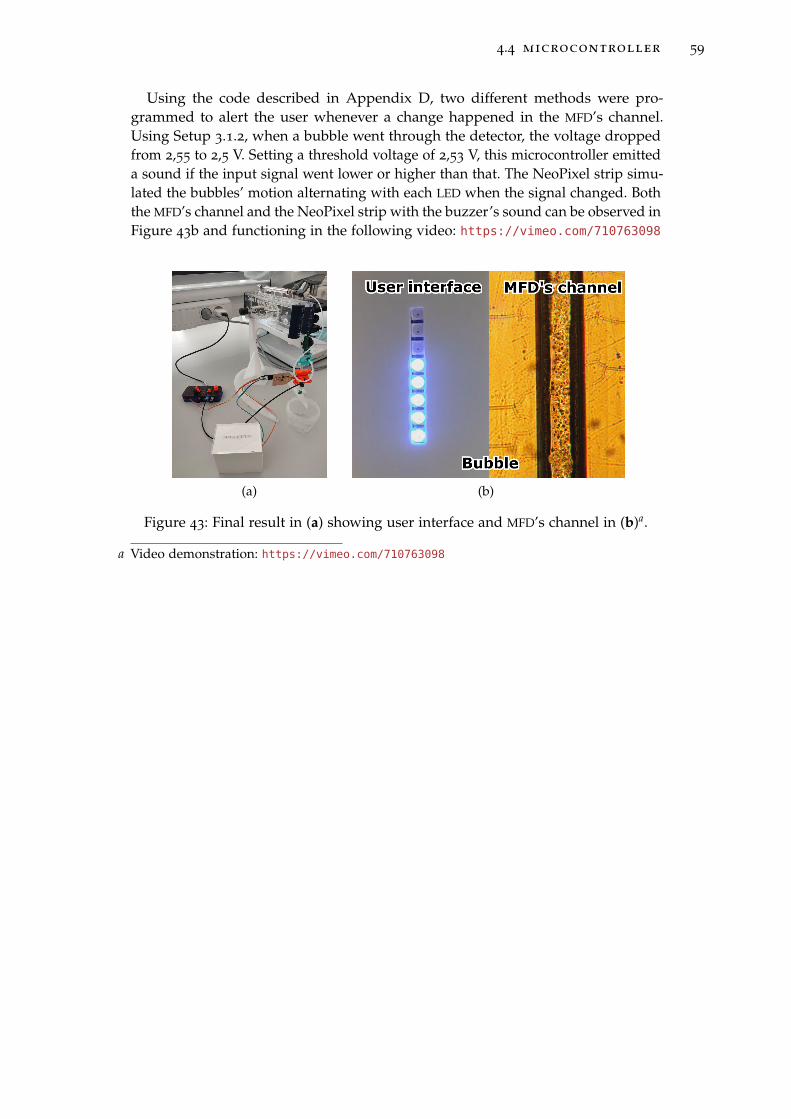
4.4 microcontroller 59
Using the code described in Appendix D, two different methods were pro-grammed to alert the user whenever a change happened in the MFD’s channel.Using Setup 3.1.2, when a bubble went through the detector, the voltage droppedfrom 2,55 to 2,5 V. Setting a threshold voltage of 2,53 V, this microcontroller emitteda sound if the input signal went lower or higher than that. The NeoPixel strip simu-lated the bubbles’ motion alternating with each LED when the signal changed. Boththe MFD’s channel and the NeoPixel strip with the buzzer’s sound can be observed inFigure 43b and functioning in the following video: https://vimeo.com/710763098
(a) (b)
Figure 43: Final result in (a) showing user interface and MFD’s channel in (b)a.
a Video demonstration: https://vimeo.com/710763098

60

5D I S C U S S I O N
5.1 general overview
This project has resulted in the fabrication of different optical detectors using opticalfibres and three main PCBs, as shown in Figure 25, which could be combined, givingup to 16 configurations. Four measurements were performed from more significantto lower changes in each configuration: light swing, bubbles, haemoglobin, andlysozyme crystals. If the first one did not work, the rest would not be conducteddue to their lower reaction with the detectors.
The additional structures depicted in Figure 26 helped during the measurementprocess. The syringe pump provided a slow flow rate but was not completelyconstant due to the use of bare hands and the connection between gear and rack,which was not ideal. Moreover, the stand with the magnet holder kept everythingin place, similar to MicroMax’s beamline setup. Finally, the control panel allowedthe switching between emitters and receivers without any complications resultingin faster measurements.
Considering all measurements, it can be observed that Setups 2 and 4 did not giveany outputs, as shown in both Figure 34 and Figure 39. After checking these lastSetups with a direct connection and a different fibre, it was observed in Figure 41
that apart from a misalignment due to different reasons as depicted in Figure 21,the connection inside the fibre adapters was not optimal to deliver enough light. Onthe other hand, Setups 1 and 3 were correctly aligned, showing response to lightchanges, but only detected when an air bubble went through, being impossibleto differentiate crystals from the floor noise. This floor noise with ±50mVpp wasmainly due to the voltage source and the connections inside the boards, which werenot entirely filtered by the low pass filter. Due to the limitations when using themilling machine using single sided boards, the layout design could be improved byadding more layers allowing better reference planes thus possibly reducing noise.Another way to limit the thermal noise would be to reduce the temperature of theoptical detector, trying not to affect the crystals.
Observing all graphs related to the bubbles, these voltage swings did not occurinstantly in some cases, leading to a longer falling time and less precision in thedetection. As depicted in Table 6, the last column shows the change in voltage dueto air bubbles related to the voltage variation when the receiver gets light or not.Only Setup 3.1.2 with the IFE98 RED emitter and VEMD1060X01 PIN shows thebest response compared to the others, with a 13,25 % of change ratio concerning thelight changes and sharper response between changes. Using the potentiometers inthis configuration, the reference voltage corresponds to 0,51 mV and the gain factoris 10,11 V/V meaning that the original received signal from these bubbles had anamplitude of 4,19 mV. The photodiode used in this configuration had a sensingarea of 0,23 mm2, which was very close to the channel’s width (0,2 mm) and thatis the reason of why the signal varies more in relation to the changes due to the
61

5.2 user interface 62
emitter switching. Keeping the mean value, observed in the graph of Figure 44, thechanges whenever a bubble went through were noticeable due to the voltage levelbeing lower than in the steady-state. As this Figure shows, the bubble’s detectionwas achieved, but it could also be calculated how big they were according to thefalling and rising edges of the signal and the buffer’s flow rate.
Figure 44: Matching between signal changes and bubbles in Setup 3.1.2.
5.2 user interface
Looking at Figure 43 and the related video, it can be observed that each changeinside the buffer due to the appearance of bubbles was detected by the ESP32 andnotified using the buzzer and the NeoPixel strip. This result shows that the userinterface was achieved, which could lead in the future to a connection with theshutter’s control system at the MAX IV Laboratory.

6C O N C L U S I O N
This chapter assesses the final development of this project, analysing whether theobjectives set out in the introduction have been achieved. It also describes the futurework that will serve to improve or complement the detector.
In order to conclude the main objective of the project, the partial objectives areanalysed. Firstly, thanks to the collaboration of the AdaptoCell project team, thespace limitations within the beamline were noted. The redirection of cables andfibre optics along a single axis to an external control panel fulfils these previouslimitations. Also, the design of the detector makes it possible to use it with differentchips without making any internal changes.
Secondly, it was possible to simulate and design two configurations for the opticaldetector, proposing different solutions for each specific case using LED light sourcesand PIN photodiodes as sensors with different adapters and waveguides.
Thirdly, tests outside the synchrotron (off-line) gave partially positive results,depending on the sample type. Bubbles inside the buffer affected the light signalsufficiently to be detected by the microcontroller. However, both microcrystalsamples (haemoglobin and lysozyme) did not produce significant changes abovethe noise floor.
Comparing these results to the ones obtained from the experiment performedby Xiang et al. [18] using embedded fibres or the one using a coulter counter byZhang et al. [19], the sensitivity from these optical detectors is greater. The opticalfibres embedded into the chip have more accuracy due to their adjustable diameterand proximity to the channel. In this project, that configuration was not possibledue to the lack of optical fibres in the market and the necessity to make this sensorinterchangeable between devices, which is not possible using other approachesdone for the moment.
In summary, using an optical sensor in a microfluidic device to detect channelchanges was successful in some cases. This indicates that, by refining the design, itis possible to increase sensitivity and detect more subtle changes.
6.1 socioeconomic impact
6.1.1 Budget
For the purpose of budgeting the project, the costs were separated according totheir involvement, i.e. material, personnel and total costs.
6.1.1.1 Material costs
On the one hand, the entire manufacturing process was carried out within theFabLab at Halmstad University. Using their budgeting method, the manufacturing
63

6.1 socioeconomic impact 64
cost corresponds to a 10% of the used materials and expendable tools as shown inTable 7.
Table 7: Fabrication costs.
Milling Laser cutting and 3d printingMaterial Price (e) Material Price (e)
Drill 0.4mm 5,10 Acrylic 36,00
Drill 0.6mm 4,30 SLA resin 20,70
Drill 1.0mm 3,70 PETG and PLA 20,00
Total 13,10 Total 76,70
Total + 10% 14,41 Total + 10% 84,37
On the other hand, the implemented optical and electronic components are listedin detail in Appendix A. As a general overview, the Table 8 indicates the total costfor each board.
Table 8: Boards costs.
Board Units Price (e) Reference
BOARD001 1 105,67 Table A1
BOARD002 A 1 16,49 Table A2
BOARD002 B 1 16,58 Table A3
BOARD002 board 1 6,82 Table A4
BOARD003 A 1 0,75 Table A6
BOARD003 B 1 0,56 Table A5
BOARD003 board 1 6,82 Table A7
Total 153,69
6.1.1.2 Personnel costs
The personnel costs involved in the realisation of the project include the salary of anelectronic engineer, about 25 e/hour. Considering the time taken to carry out thisproject, comprising 440 hours, and the involvement of two engineers, the personnelcosts amount to 22,000 e.
6.1.1.3 Total costs
Finally, the total price for the preparation of the project amounts to the sum of22252,47 e, as shown in the following Table.

6.1 socioeconomic impact 65
Table 9: Budget summary.
Description Total Cost (e)
Material costs 252,47
Personnel costs 22000,00
Total budget 22252,47
6.1.2 Sustainability Impact
The advance in today’s technology has been remarkable. New products are devel-oped that incorporate significant improvements over their predecessors, resultingin a high turnover of electronic devices. Commercial products are often replaced asa whole or in large parts before being repaired. All these discarded electronics aregrowing at two million metric tonnes per year as depicted in Figure 45.
By creating a portable detector capable of changing the microfluidic device, thisproject reduces the amount of generated e-waste.
Figure 45: Worldwide increases in electronic waste, by million metric tonnes. Itshows an increase of two million metric tonnes per year [25].
6.1.3 Social Impact
Thanks to the use of microfluidics, not only it is useful for systems downsizing, butit has proven to be a great help in different areas, such as growing artificial organsin medicine or the discovery of new cosmetics [26].
Nowadays, the incorporation of crystallography within microfluidics has allowedsociety to have a more in-depth knowledge of the world around us. The most recentexample deals with the SARS-CoV-2 pandemic. With this technique, scientist couldstudy the structure and response of this virus, as well as conformations of its mainprotease active site for improved drug repurposing [27, 28].

6.1 socioeconomic impact 66
This would improve society in many aspects, not just human health, but alsocreate new materials that help us in our daily lives. For example, in 1982, DanShechtman discovered the quasi-crystal with the properties of low friction andlow surface reactivity, which were used to create non-sticking frying pans, surgeryinstruments and even LED lights. In addition, crystallography can help understandthe properties of structures such as graphene or how haemoglobin changes whencarrying oxygen particles. The technique can be carried out in space for sampleanalysis to search hint of life.
Finally, the completion of this project would improve the quality of the dataobtained through this crystallography process, determining when an image isrelated to a crystal and not to an empty space. A beneficial side effect would be thereduction of memory usage as the empty images occupy a significant amount of it.
6.1.4 Future work
In order to continue with the development of the present project, several ideas andproposals emerged that would improve the functioning of the optical detector:
• Optical fibres: use more advanced means to align the fibres. Also, improvethe quality of the connection with the adapter or adjust both the diameterand the power of the transmitted light. Lenses were out of the scope of thisproject due to time limitations, but they would improve the light focus intothe channel.
• Electronic design: reduce ambient noise as much as possible to be able todifferentiate signals of lower amplitude.
• Implementation in MicroMax: replace the LED indicator with communica-tion to the computer system used in MicroMax to alternate the opening andclosing of the X-ray shutter.

B I B L I O G R A P H Y
[1] Max iv laboratory. adaptocell [internet]. lund; 2021 [cited 2022-5-13]. retrieved from: https://portal.research.lu.se/en/projects/
adaptocell-for-max-iv-laboratory-users.
[2] M S Smyth and J H J Martin. x Ray crystallography. Molecular Pathology, 53(1):8–14, February 2000.
[3] Piero Macchi. Cryo-Crystallography: Diffraction at Low Temperature andMore. In Kari Rissanen, editor, Advanced X-Ray Crystallography, pages 33–67.Springer, Berlin, Heidelberg, 2012.
[4] James S. Fraser, Henry van den Bedem, Avi J. Samelson, P. Therese Lang,James M. Holton, Nathaniel Echols, and Tom Alber. Accessing protein confor-mational ensembles using room-temperature x-ray crystallography. Proceedingsof the National Academy of Sciences, 108(39):16247–16252, 2011.
[5] Ki Hyun Nam. Approach of serial crystallography. Crystals, 10(10), 2020.
[6] Harleen Kaur, Sonali Bhagwat, Tarun Sharma, and Amit Kumar. Analyticaltechniques for characterization of biological molecules - Proteins and ap-tamers/oligonucleotides. Bioanalysis, 11, November 2018. Figure 2. Schematicdiagram for characterization of protein using x-ray crystallography; p. 11.
[7] Naga S. Korivi and Li Jiang. A Generic Chip-to-World Fluidic InterconnectSystem for Microfluidic Devices. In 2007 Thirty-Ninth Southeastern Symposiumon System Theory, pages 176–180, March 2007.
[8] Volodymyr Novikov, Olha Shved, Veronica Chervetsova, Ivanna Lobur, andSofiya Matviykiv. Microfluidic lab-chip devices for biotechnological applica-tions. In Perspective Technologies and Methods in MEMS Design, pages 227–229,May 2011.
[9] Pamela N. Nge, Chad I. Rogers, and Adam T. Woolley. Advances in Microflu-idic Materials, Functions, Integration, and Applications. Chemical Reviews, 113
(4):2550–2583, April 2013. Publisher: American Chemical Society.
[10] Ali Rezaei and Ricardo Izquierdo. Rapid prototyping of microfluidic devicesand their applications. In 2018 16th IEEE International New Circuits and SystemsConference (NEWCAS), pages 385–389, June 2018.
[11] Anatoly Evstrapov, Vladimir Kurochkin, Dmitry Petrov, and Sergey Sheptunov.Microfluidic Devices for Molecular Diagnostics in Medical and BiologicalResearch. In 2018 3rd Russian-Pacific Conference on Computer Technology andApplications (RPC), pages 1–4, August 2018.
67

bibliography 68
[12] Pushparani Micheal Raj, Laurent Barbe, Martin Andersson, Milena De Al-buquerque Moreira, Dörthe Haase, James Wootton, Susan Nehzati, Ann ETerry, Ross J Friel, Maria Tenje, et al. Fabrication and characterisation of asilicon-borosilicate glass microfluidic device for synchrotron-based hard x-rayspectroscopy studies. RSC Advances, 11(47):29859–29869, 2021.
[13] Hongpeng Zhang, Chan Hee Chon, Xinxiang Pan, and Dongqing Li. Methodsfor counting particles in microfluidic applications. Microfluidics and Nanofluidics,7:739, August 2009.
[14] Nicole Pamme, Ryuji Koyama, and Andreas Manz. Counting and sizing ofparticles and particle agglomerates in a microfluidic device using laser lightscattering. Lab on a Chip, 3(3):187–192, August 2003.
[15] Dawn Schafer, Emily A. Gibson, Evan A. Salim, Amy E. Palmer, Ralph Jimenez,and Jeff Squier. Microfluidic cell counter with embedded optical fibers fabri-cated by femtosecond laser ablation and anodic bonding. Optics Express, 17(8):6068–6073, April 2009.
[16] Qing Xiang, Xiangchun Xuan, Bo Xu, and Dongqing Li. Multi FunctionalParticle Detection with Embedded Optical Fibers in a Poly(dimethylsiloxane)Chip. Instrumentation Science and Technology, 33(5):597–607, September 2005.
[17] Dawn Schafer, Emily A. Gibson, Evan A. Salim, Amy E. Palmer, Ralph Jimenez,and Jeff Squier. Microfluidic cell counter with embedded optical fibers fabri-cated by femtosecond laser ablation and anodic bonding. Optics Express, 17
(8):6068–6073, April 2009. Figure 2 (a). White light image of the fluid channel(horizontal) with four fiber grooves: one above at 14 degrees from normal andthree below at -45, 0, and 45 degrees from normal; p. 4.
[18] Qing Xiang, Xiangchun Xuan, Bo Xu, and Dongqing Li. Multi FunctionalParticle Detection with Embedded Optical Fibers in a Poly(dimethylsiloxane)Chip. Instrumentation Science and Technology, 33(5):597–607, September 2005.Figure 2 (b). The reduction of the optical loss by PDMS filling; p. 6.
[19] Wenchang Zhang, Yuan Hu, Gihoon Choi, Shengfa Liang, Ming Liu, andWeihua Guan. Microfluidic multiple cross-correlated Coulter counter forimproved particle size analysis. Sensors and Actuators B: Chemical, 296:126615,October 2019.
[20] Yongxin Song, Junyan Zhang, and Dongqing Li. Microfluidic and NanofluidicResistive Pulse Sensing. Micromachines, 8(7):204, July 2017.
[21] Yongxin Song, Hongpeng Zhang, and Mengqi Li. Microfluidic Resistive PulseSensor. In Dongqing Li, editor, Encyclopedia of Microfluidics and Nanofluidics,pages 1993–2000. Springer, New York, NY, 2015.
[22] L. L. Sohn, O. A. Saleh, G. R. Facer, A. J. Beavis, R. S. Allan, and D. A.Notterman. Capacitance cytometry: Measuring biological cells one by one.Proceedings of the National Academy of Sciences, 97(20):10687–10690, September2000.

bibliography 69
[23] David K. Lynch, William Charles Livingston, and William Livingston. Colorand Light in Nature. Cambridge University Press, June 2001.
[24] Paula trindell. a variety of mismatches cause losses in a fiber-to-fiber connection. [figure]. [cited 2022 may 10]. available from:https://www.photonics.com/Articles/Connectors_and_Splices_Correct_
Alignment_Spells/a25152.
[25] Tco certified. global e-waste reaches record high, says new un report [inter-net]; sweden. 2015 [cited 2022-5-14]. retrieved from: https://discord.com/channels/@me/337525774229831682/974970523933081660.
[26] Chang-Soo Lee. Grand challenges in microfluidics: A call for biological andengineering action. Frontiers in Sensors, 1, 2020.
[27] Serdar Durdagi, Cagdas Dag, Berna Dogan, Merve Yigin, Timucin Avsar,Cengizhan Buyukdag, and et al. Near-physiological-temperature serial crys-tallography reveals conformations of sars-cov-2 main protease active site forimproved drug repurposing. Structure, 29(12):1382–1396.e6, 2021.
[28] Nayim Sepay, Pranab Chandra Saha, Zarrin Shahzadi, Aratrika Chakraborty,and Umesh Chandra Halder. A crystallography-based investigation of weakinteractions for drug design against COVID-19. Physical Chemistry ChemicalPhysics, 23(12):7261–7270, April 2021. Publisher: The Royal Society of Chem-istry.

AB O M

APPENDIX A Bill Of Materials (BOM)
Tabl
eA
1:B
OM
for
BOA
RD
001
(all
vari
ants
)
Des
crip
tion
Des
igna
tor
Qua
ntit
yM
anuf
actu
rer
Part
Num
ber
Uni
tPr
ice
(e)
Tota
lPr
ice
(e)
0.1µ
F±
10
%1
6V
Cer
amic
Cap
acit
orX
7R
12
06
(32
16
Met
ric)
C1
,C2
,C3
38
85
01
22
08
03
00
,11
0,3
3
Led
Fibe
rO
ptic
50
MBP
S6
50N
MR
edD
11
IF-E
98
13
,39
13
,39
Fibe
rop
tic
rece
iver
-Met
alST
Rec
epta
cle,
Ope
rati
ngTe
mpe
ratu
re:-
40
°C
-8
5Â
°C,T
O-1
8-3
,RoH
SD
21
OPF
52
21
9,1
91
9,1
9
Yello
wPC
Test
Poin
t,M
inia
ture
Phos
phor
Bron
zeSi
lver
Plat
ing
0.0
40
"(1
.02
mm
)H
ole
Dia
met
erM
ount
ing
Type
J1,J
3,J
6,J
74
50
04
0,4
01
,60
Fibe
rO
ptic
Tran
smit
ter
82
0nm
1.7
V1
00
mA
STJ2
1H
FBR
-14
14
TZ2
6,9
52
6,9
5
Con
nect
orH
eade
rTh
roug
hH
ole
2po
siti
on0
.10
0"
(2.5
4m
m)
J41
KW
AF-
WD
S-0
22
51
-01
-XX
X0
,19
0,1
9
Con
nU
nshr
oude
dH
eade
rH
DR
4PO
S2
.54
mm
Sold
erR
AT
hru-
Hol
eJ5
1PH
1R
A-0
4-U
A0
,18
0,1
8
REC
EIV
ERFI
BER
OPT
12
5M
HZ
AN
AST
/R
XO
ptic
alFi
ber
16
0M
Bd8
-Pin
J81
HFB
R-2
41
6TZ
26
,09
26
,09
43
Ohm
s±
5%
0.2
5W
,1/4
WC
hip
Res
isto
r1
20
6(3
21
6M
etri
c)A
utom
otiv
eA
EC-Q
20
0Th
ick
Film
R1
1R
MC
F12
06
JT4
3R
00
,10
0,1
0
16
0O
hms±
5%
0.2
5W
,1/4
WC
hip
Res
isto
r1
20
6(3
21
6M
etri
c)A
utom
otiv
eA
EC-Q
20
0T
hick
Film
R2
1R
MC
F12
06
JT1
60
R0
,10
0,1
0
24
kOhm
s±
5%
0.2
5W
,1/4
WC
hip
Res
isto
r1
20
6(3
21
6M
etri
c)A
utom
otiv
eA
EC-Q
20
0T
hick
Film
R3
1R
MC
F12
06
JT2
4K
00
,10
0,1
0
68
0O
hms±
5%
0.2
5W
,1/4
WC
hip
Res
isto
r1
20
6(3
21
6M
etri
c)A
utom
otiv
eA
EC-Q
20
0T
hick
Film
R4
1R
MC
F12
06
JT6
80
R0
,10
0,1
0
27
0O
hms±
5%
0.2
5W
,1/4
WC
hip
Res
isto
r1
20
6(3
21
6M
etri
c)A
utom
otiv
eA
EC-Q
20
0T
hick
Film
R5
1R
MC
F12
06
JT2
70
R0
,10
0,1
0
0O
hms
Jum
per
0.2
5W
,1/4
WC
hip
Res
isto
r1
20
6(3
21
6M
etri
c)A
utom
otiv
eA
EC-Q
20
0T
hick
Film
R6
,R7
1R
MC
F12
06
ZT
0R
00
0,1
00
,10
10
0O
hms±
5%
0.2
5W
,1/4
WC
hip
Res
isto
r1
20
6(3
21
6M
etri
c)A
utom
otiv
eA
EC-Q
20
0T
hick
Film
R8
1R
MC
F12
06
JT1
00
R0
,10
0,1
0
1O
hms±
1%
0.2
5W
,1/4
WC
hip
Res
isto
r1
20
6(3
21
6M
etri
c)A
utom
otiv
eA
EC-Q
20
0Th
ick
Film
R9
1R
MC
F12
06
FT1
R0
00
,10
0,1
0
Swit
chSl
ide
ON
ON
ON
SP3
TTo
pSl
ide
0.1
A1
2V
DC
10
00
0C
ycle
sPC
Pins
Thr
ough
Hol
eBu
lkSW
1,S
W2
,SW
33
OS1
03
01
1M
S8Q
P10
,64
1,9
2
Inst
rum
enta
tion
Am
plifi
er1
Cir
cuit
Rai
l-to
-Rai
l8-S
OIC
U1
1M
AX
44
61
TESA
+T4
,92
4,9
2
Inst
rum
enta
tion
Am
plifi
er1
Cir
cuit
Rai
l-to
-Rai
l8-S
OIC
(Adj
usta
ble
Gai
n)U
1’
1M
AX
44
60
ESA
+3
,97
3,9
7
10
mm
,1kÎ
©1
MΩ
,Pan
elM
ount
,Rot
ary
Pote
ntio
met
erV
R1
1PT
01
-D1
15
D-B
10
40
,76
0,7
6
Res
Cer
met
Trim
mer
20
KO
hm2
5%
1/2
0W
1(E
lec)
/1(M
ech)
Turn
1.9
mm
(3.4
X3
.5X
2m
m)
J-H
ook
SMD
T/R
VR
21
32
03
X2
03P
2,6
92
,69
Res
Cer
met
Trim
mer
10
0K
Ohm
25
%1
/20
W1
.9m
m(3
.4X
3.5
X2
mm
)J-
Hoo
kSM
DT
/RV
R3
11
62
39
16
-42
,69
2,6
9
Fibe
rO
ptic
Cab
leBl
ack
POF
10
00µ
m1
6.4
0’(
5.0
0m
)O
F11
MIK
RO
E-1
47
31
3,4
71
3,4
7
RS
PRO
STto
Unt
erm
inat
edSi
mpl
exM
ulti
Mod
eO
M1
Fibe
rO
ptic
Cab
le,6
2.5
/1
25
ÎŒm
,Bla
ck,1
mO
F22
53
5-7
53
16
,50
13
,00
Prin
ted
circ
uit
boar
dep
oxy
16
0x1
00
mm
,Sca
nkem
iBR
D0
01
11
10
04
16
,82
TO
TAL
CO
STO
FM
AT
ERIA
LSFO
RB
OA
RD001
105,67

APPENDIX A BOM
Tabl
eA
2:B
OM
for
BOA
RD
002
and
bigg
erph
otod
iode
(all
vari
ants
)
Des
crip
tion
Des
igna
tor
Qua
ntit
yM
anuf
actu
rer
Part
Num
ber
Uni
tPr
ice
Tota
lPri
ce
0.1µ
F±
10
%1
6V
Cer
amic
Cap
acit
orX
7R
12
06
(32
16
Met
ric)
C1
,C2
,C3
,C4
48
85
01
22
08
03
00
,11
0,4
4
Phot
odio
de6
20
nm-
12
0Â
°0
80
5(2
01
2M
etri
c)D
11
SFH
27
16
0,8
00
,80
Con
nU
nshr
oude
dH
eade
rH
DR
4PO
S2.5
4m
mSo
lder
RA
Thru
-Hol
eJ1
1PH
1R
A-0
4-U
A0
,18
0,1
8
24
kOhm
s±
5%
0.2
5W
,1/4
WC
hip
Res
isto
r1
20
6(3
21
6M
etri
c)A
utom
otiv
eA
EC-Q
20
0Th
ick
Film
R1
1R
MC
F12
06
JT2
4K
00
,10
0,1
0
68
0O
hms±
5%
0.2
5W
,1/4
WC
hip
Res
isto
r1
20
6(3
21
6M
etri
c)A
utom
otiv
eA
EC-Q
20
0Th
ick
Film
R2
1R
MC
F12
06
JT6
80
R0
,10
0,1
0
27
0O
hms±
5%
0.2
5W
,1/4
WC
hip
Res
isto
r1
20
6(3
21
6M
etri
c)A
utom
otiv
eA
EC-Q
20
0Th
ick
Film
R3
1R
MC
F12
06
JT2
70
R0
,10
0,1
0
0O
hms
Jum
per
0.2
5W
,1/4
WC
hip
Res
isto
r1
20
6(3
21
6M
etri
c)A
utom
otiv
eA
EC-Q
20
0Th
ick
Film
R4,R
51
RM
CF1
20
6Z
T0R
00
0,1
00
,10
10
0O
hms±
5%
0.2
5W
,1/4
WC
hip
Res
isto
r1
20
6(3
21
6M
etri
c)A
utom
otiv
eA
EC-Q
20
0Th
ick
Film
R6
1R
MC
F12
06
JT1
00
R0
,10
0,1
0
1O
hms±
1%
0.2
5W
,1/4
WC
hip
Res
isto
r1
20
6(3
21
6M
etri
c)A
utom
otiv
eA
EC-Q
20
0Th
ick
Film
R7
1R
MC
F12
06
FT1
R0
00
,10
0,1
0
28
0O
hms±
1%
0.2
5W
,1/4
WC
hip
Res
isto
r1
20
6(3
21
6M
etri
c)A
utom
otiv
eA
EC-Q
20
0Th
ick
Film
R8,R
92
RM
CF1
20
6FT
28
0R
0,1
00
,20
Inst
rum
enta
tion
Am
plifi
er1
Cir
cuit
Rai
l-to
-Rai
l8-S
OIC
U1
1M
AX
44
61
TESA
+T4
,92
4,9
2
Inst
rum
enta
tion
Am
plifi
er1
Cir
cuit
Rai
l-to
-Rai
l8-S
OIC
(Adj
usta
ble
Gai
n)U
1’
1M
AX
44
60
ESA
+3
,97
3,9
7
Res
Cer
met
Trim
mer
20
KO
hm2
5%
1/2
0W
1(E
lec)
/1(M
ech)
Turn
1.9
mm
(3.4
X3
.5X
2m
m)
J-H
ook
SMD
T/R
VR
11
32
03
X2
03
P2
,69
2,6
9
Res
Cer
met
Trim
mer
10
0K
Ohm
25
%1/2
0W
1.9
mm
(3.4
X3
.5X
2m
m)
J-H
ook
SMD
T/R
VR
21
16
23
91
6-4
2,6
92
,69
TO
TAL
CO
STO
FM
AT
ERIA
LSFO
RB
OA
RD001
AN
DB
IGG
ERSM
DPH
OT
OD
IOD
E1
6,4
9

APPENDIX A BOM
Tabl
eA
3:B
OM
for
BOA
RD
002
and
smal
ler
phot
odio
de(a
llva
rian
ts)
Des
crip
tion
Des
igna
tor
Qua
ntit
yM
anuf
actu
rer
Part
Num
ber
Uni
tPr
ice
(e)
Tota
lPri
ce(e
)
0.1µ
F±
10
%1
6V
Cer
amic
Cap
acit
orX
7R
12
06
(32
16
Met
ric)
C1,C
2,C
3,C
44
88
50
12
20
80
30
0,1
10
,44
Phot
odio
de8
20
nm6
0ns
14
0Â
°0
80
5(2
01
2M
etri
c)D
11
VEM
D1
06
0X
01
0,8
90
,89
Con
nU
nshr
oude
dH
eade
rH
DR
4PO
S2.5
4m
mSo
lder
RA
Thru
-Hol
eJ1
1PH
1R
A-0
4-U
A0
,18
0,1
8
24
kOhm
s±
5%
0.2
5W
,1/4
WC
hip
Res
isto
r1
20
6(3
21
6M
etri
c)A
utom
otiv
eA
EC-Q
20
0Th
ick
Film
R1
1R
MC
F12
06
JT2
4K
00
,10
0,1
0
68
0O
hms±
5%
0.2
5W
,1/4
WC
hip
Res
isto
r1
20
6(3
21
6M
etri
c)A
utom
otiv
eA
EC-Q
20
0Th
ick
Film
R2
1R
MC
F12
06
JT6
80
R0
,10
0,1
0
27
0O
hms±
5%
0.2
5W
,1/4
WC
hip
Res
isto
r1
20
6(3
21
6M
etri
c)A
utom
otiv
eA
EC-Q
20
0Th
ick
Film
R3
1R
MC
F12
06
JT2
70
R0
,10
0,1
0
0O
hms
Jum
per
0.2
5W
,1/4
WC
hip
Res
isto
r1
20
6(3
21
6M
etri
c)A
utom
otiv
eA
EC-Q
20
0Th
ick
Film
R4,R
51
RM
CF1
20
6Z
T0R
00
0,1
00
,10
10
0O
hms±
5%
0.2
5W
,1/4
WC
hip
Res
isto
r1
20
6(3
21
6M
etri
c)A
utom
otiv
eA
EC-Q
20
0Th
ick
Film
R6
1R
MC
F12
06
JT1
00
R0
,10
0,1
0
1O
hms±
1%
0.2
5W
,1/4
WC
hip
Res
isto
r1
20
6(3
21
6M
etri
c)A
utom
otiv
eA
EC-Q
20
0Th
ick
Film
R7
1R
MC
F12
06
FT1
R0
00
,10
0,1
0
28
0O
hms±
1%
0.2
5W
,1/4
WC
hip
Res
isto
r1
20
6(3
21
6M
etri
c)A
utom
otiv
eA
EC-Q
20
0Th
ick
Film
R8,R
92
RM
CF1
20
6FT
28
0R
0,1
00
,20
Inst
rum
enta
tion
Am
plifi
er1
Cir
cuit
Rai
l-to
-Rai
l8-S
OIC
U1
1M
AX
44
61
TESA
+T4
,92
4,9
2
Inst
rum
enta
tion
Am
plifi
er1
Cir
cuit
Rai
l-to
-Rai
l8-S
OIC
(Adj
usta
ble
Gai
n)U
1’
1M
AX
44
60
ESA
+3
,97
3,9
7
Res
Cer
met
Trim
mer
20
KO
hm2
5%
1/2
0W
1(E
lec)
/1(M
ech)
Turn
1.9
mm
(3.4
X3
.5X
2m
m)
J-H
ook
SMD
T/R
VR
11
32
03
X2
03
P2
,69
2,6
9
Res
Cer
met
Trim
mer
10
0K
Ohm
25
%1/2
0W
1.9
mm
(3.4
X3
.5X
2m
m)
J-H
ook
SMD
T/R
VR
21
16
23
91
6-4
2,6
92
,69
TO
TAL
CO
STO
FM
AT
ERIA
LSFO
RB
OA
RD002
AN
DSM
ALL
ERSM
DPH
OT
OD
IOD
E1
6,5
8
Tabl
eA
4:S
hare
dm
ater
ialf
orbo
thBO
AR
D002.
Des
crip
tion
Des
igna
tor
Qua
ntit
yM
anuf
actu
rer
Part
Num
ber
Uni
tPr
ice
(e)
Tota
lPri
ce(e
)
Prin
ted
circ
uit
boar
dep
oxy
16
0x1
00
mm
,Sca
nkem
iBR
D0
02
11
10
04
16
,82
6,8
2

APPENDIX A BOM
Tabl
eA
5:B
OM
for
BOA
RD
003
and
IRLE
D(a
llva
rian
ts)
Des
crip
tion
Des
igna
tor
Qua
ntit
yM
anuf
actu
rer
Part
Num
ber
Uni
tPr
ice
(e)
Tota
lPri
ce(e
)
Infr
ared
(IR
)Em
itte
r850nm
1.4
V70
mA
0.5
mW
/sr
@20m
A140Â
°0603
(1608
Met
ric)
D1
115406085
BA400
A0
,46
0,4
6
Con
nect
orH
eade
rT
hrou
ghH
ole
2po
siti
on0
.100
"(2
.54m
m)
J11
KW
AF-
WD
S-02251
-01
-XX
X0
,19
0,1
9
150
Ohm
s±
5%
0.2
5W
,1/4
WC
hip
Res
isto
r1206
(3216
Met
ric)
Aut
omot
ive
AEC
-Q200
Thic
kFi
lmR
11
RM
CF1
206
JT150
R0
,10
0,1
0
TO
TAL
CO
STO
FM
AT
ERIA
LSFO
RB
OA
RD003
WIT
HIR
LED
0,7
5
Tabl
eA
6:B
OM
for
BOA
RD
003
and
RED
LED
(all
vari
ants
)
Des
crip
tion
Des
igna
tor
Qua
ntit
yM
anuf
actu
rer
Part
Num
ber
Uni
tPr
ice
(e)
Tota
lPri
ce(e
)
Red
LED
Indi
cati
on-
Dis
cret
e2V
0603
(1608
Met
ric)
D1
1SM
L-3
10
VTT
86
0,2
70
,27
Con
nect
orH
eade
rT
hrou
ghH
ole
2po
siti
on0
.100
"(2
.54m
m)
J11
KW
AF-
WD
S-02251
-01
-XX
X0
,19
0,1
9
180
Ohm
s±
5%
0.2
5W
,1/4
WC
hip
Res
isto
r1206
(3216
Met
ric)
Aut
omot
ive
AEC
-Q200
Thic
kFi
lmR
11
RM
CF1
206
JT180
R0
,10
0,1
0
TO
TAL
CO
STO
FM
AT
ERIA
LSFO
RB
OA
RD003
WIT
HR
EDLE
D0
,56
Tabl
eA
7:S
hare
dm
ater
ialf
orbo
thBO
AR
D003.
Des
crip
tion
Des
igna
tor
Qua
ntit
yM
anuf
actu
rer
Part
Num
ber
Uni
tPr
ice
Tota
lPri
ce
Prin
ted
circ
uit
boar
dep
oxy
160x1
00
mm
,Sca
nkem
iBR
D0
03
1110041
6,8
2
Fabr
icat
ion
ofth
ebo
ard
usin
gde
skto
pm
illin
gm
achi
ne1

BB O A R D S L AY O U T
A
A
B
B
C
C
D
D
E
E
1 1
2 2
3 3
4 4
BOARD 001
J8
J2
D1
J7J6
J3
J1
J5
J4
SW3
SW2
SW1
J8
J2
VR1
D1
D2
TOP SIDE
R4
R2
R1
R9
R8
R7
R6
R5
R3
U1
C3
C2
C1
VR2
VR3
BOTTOM SIDE
Figure B1: Board 001 Layout and assembly drawings.A
A
B
B
C
C
D
D
E
E
1 1
2 2
3 3
4 4
BOARD 002
J1J1
BOTTOM SIDE
R2 R9
R8
R7
R6
R5R
4R
3
R1
D1
U1
C4C3
C2
C1
VR2
VR1
TOP SIDE
Figure B2: Board 002 Layout and assembly drawings.

APPENDIX B BOARDS LAYOUT
A
A
B
B
C
C
D
D
E
E
1 1
2 2
3 3
4 4
J1
BOTTOM SIDE
R1
D1
TOP SIDE
BOARD 003
Figure B3: Board 003 Layout and assembly drawings.

CM AT L A B C O D E
Listing C1: Code used for extracting Setup 1.1.1 signals.
1 %-----PLOTTING FROM XLSX GENERATED IN OSCILLOSCOPE-----%
w1=0.7;
w2=1.5;
lag = 100;
%---SETUP 1.1.1---%
6 Setup_1_1_1_LI = readtable(’Setups.xlsx’,’Sheet’,’Setup 1’, ’Range’, ’A
5:B40005’);
Setup_1_1_1_B = readtable(’Setups.xlsx’,’Sheet’,’Setup 1’, ’Range’, ’D
5:E40005’);
Setup_1_1_1_H = readtable(’Setups.xlsx’,’Sheet’,’Setup 1’, ’Range’, ’G
5:H40005’);
Setup_1_1_1_L = readtable(’Setups.xlsx’,’Sheet’,’Setup 1’, ’Range’, ’J
5:K40005’);
11 %PLOT 1_1_1%
%LIGHT%
figure
hold on
16 time_li = Setup_1_1_1_LI.Time; %: light time
voltage_li = Setup_1_1_1_LI.Voltage; %: light voltage
plot(time_li,voltage_li,’Color’, 1/255*[180,0,255] ,’LineWidth’,w1)
21 xlim([0 20])
ylim([1.5 4.5])
ylabel(’Voltage [V]’)
xlabel(’Time [s]’)
legend(’Oscilloscope’)
26 hold off
%BUBBLES%
figure
hold on
31 time_b = Setup_1_1_1_B.Time; %: bubble time
voltage_b = Setup_1_1_1_B.Voltage; %: bubble voltage
simple = movavg(voltage_b,’simple’,lag);

APPENDIX C MATLAB CODE
plot(time_b,voltage_b,’Color’, 1/255*[0,100,255] ,’LineWidth’,w1)
36 plot(time_b,simple,’Color’,1/255*[0,0,255],’LineWidth’,w2)
xlim([0 20])
ylim([3.8 4.1])
ylabel(’Voltage [V]’)
41 xlabel(’Time [s]’)
legend(’Oscilloscope’,’Mean value’)
hold off
%HAEMOGLOBIN%
46 figure
hold on
time_h = Setup_1_1_1_H.Time; %: haemoglobin time
voltage_h = Setup_1_1_1_H.Voltage; %: haemoglobin voltage
simple = movavg(voltage_h,’simple’,lag);
51
plot(time_h,voltage_h,’Color’, 1/255*[128,255,0] ,’LineWidth’,w1)
plot(time_h,simple,’Color’,1/255*[51,102,0],’LineWidth’,w2)
xlim([0 20])
56 ylim([4.6 4.9])
ylabel(’Voltage [V]’)
xlabel(’Time [s]’)
legend(’Oscilloscope’,’Mean value’)
hold off
61
%LYSOZIME%
figure
hold on
time_l = Setup_1_1_1_L.Time; %: lysozime time
66 voltage_l = Setup_1_1_1_L.Voltage; %: lysozime voltage
simple = movavg(voltage_l,’simple’,lag);
plot(time_l,voltage_l,’Color’, 1/255*[255,100,0] ,’LineWidth’,w1)
plot(time_l,simple,’Color’,1/255*[255,0,0],’LineWidth’,w2)
71
xlim([0 20])
ylim([4.6 4.9])
ylabel(’Voltage [V]’)
xlabel(’Time [s]’)
76 legend(’Oscilloscope’,’Mean value’)
hold off

DE S P 3 2 C O D E
Listing D1: Code used for showing bubble changes with the ESP32.
3
# include <NeoPixelBus . h>
TaskHandle_t Task1 ;TaskHandle_t Task2 ;
8 # def ine BUILTIN_LED_PIN 13
# def ine INDICATION_LED_PIN 12
# def ine TONE_OUTPUT_PIN 21
# def ine TONE_PWM_CHANNEL 0 // The ESP32 has 16 channels which can generate 16 independentwaveforms. We’ll just choose PWM channel 0 here
# def ine BEEP_DURATION_MS 50
13 # def ine ALIVE_LED_DURATION 1000
# def ine MEASURE_INTERVAL_MS 2
# def ine NEOPIXEL_INTERVAL_MS 300
18
# def ine MEAN_NUMREADINGS 20
# def ine DETECTOR_SIGNAL_PIN 26
# def ine NEOPIXEL_PIN 32
23 # def ine NUMPIXELS 8
bool f a l l i n g _ s i g n a l = f a l s e ;bool r i s i n g _ s i g n a l = f a l s e ;
28 bool l a s t R i s i n g = f a l s e ;bool l a s t F a l l i n g = f a l s e ;
bool BubbleArray [ 8 ] = f a l s e , f a l s e , f a l s e , f a l s e , f a l s e , f a l s e , f a l s e , f a l s e ;33
bool s t a r t u p=true ;
long lastTimeACQ = 0 ;long lastTimeAlive = 0 ;
38 long lastTimeNeopixel = 0 ;
i n t reading = 0 ;f l o a t v o l t s = 0 ;
43 f l o a t mean_volts = 0 ;i n t num_readings = 0 ;f l o a t t o t a l = 0 ;
48 const u i n t 1 6 _ t PixelCount = 8 ; // this example assumes 4 pixels , making it smaller will cause a failureconst u i n t 8 _ t P i x e l P i n = 3 2 ; // make sure to set this to the correct pin, ignored for Esp8266
NeoPixelBus <NeoGrbFeature , Neo800KbpsMethod> s t r i p ( PixelCount , P i x e l P i n ) ;53
RgbColor blue ( 0 , 0 , 35 ) ;RgbColor black ( 0 ) ;
58 void setup ( ) S e r i a l . begin ( 1 1 5 2 0 0 ) ;pinMode ( BUILTIN_LED_PIN , OUTPUT) ;pinMode ( INDICATION_LED_PIN , OUTPUT) ;ledcAttachPin (TONE_OUTPUT_PIN, TONE_PWM_CHANNEL) ;
63
//create a task that will be executed in the Task1code() function , with priority 1 and executed on core0
xTaskCreatePinnedToCore (Task1code , /* Task function. */" Task1 " , /* name of task. */
68 10000 , /* Stack size of task */NULL, /* parameter of the task */1 , /* priority of the task */&Task1 , /* Task handle to keep track of created task */0 ) ; /* pin task to core 0 */

APPENDIX D ESP32 CODE
73 delay ( 5 0 0 ) ;
//create a task that will be executed in the Task2code() function , with priority 1 and executed on core1
xTaskCreatePinnedToCore (Task2code , /* Task function. */
78 " Task2 " , /* name of task. */10000 , /* Stack size of task */NULL, /* parameter of the task */1 , /* priority of the task */&Task2 , /* Task handle to keep track of created task */
83 1 ) ; /* pin task to core 1 */delay ( 5 0 0 ) ;
s t r i p . Begin ( ) ;s t r i p . Show ( ) ;
88
//Task1code: blinks an LED every 1000 msvoid Task1code ( void * pvParameters )
S e r i a l . p r i n t ( " Task1 running on core " ) ;93 S e r i a l . p r i n t l n ( xPortGetCoreID ( ) ) ;
f o r ( ; ; ) reading = analogRead (DETECTOR_SIGNAL_PIN) ;v o l t s = ( reading * 3 . 3 ) / 4096 ;
98 t o t a l = t o t a l + v o l t s ;i f ( num_readings < MEAN_NUMREADINGS)
num_readings ++; e l s e
103 num_readings = 0 ;mean_volts = t o t a l / MEAN_NUMREADINGS;t o t a l = 0 ;//Serial.println(mean_volts);
108
i f ( mean_volts > 2 . 5 3 )
i f ( ! l a s t R i s i n g )
113 l a s t R i s i n g = true ;r i s i n g _ s i g n a l = true ;//Serial.println("Rising edge");
l a s t F a l l i n g = f a l s e ;
118 e l s e i f ( mean_volts <= 2 . 5 3 )
i f ( ! l a s t F a l l i n g )
l a s t F a l l i n g = true ;123 f a l l i n g _ s i g n a l = true ;
//Serial.println("Falling edge");l a s t R i s i n g = f a l s e ;
128
vTaskDelay (MEASURE_INTERVAL_MS) ;
133 //Task2code: blinks an LED every 700 msvoid Task2code ( void * pvParameters )
S e r i a l . p r i n t ( " Task2 running on core " ) ;S e r i a l . p r i n t l n ( xPortGetCoreID ( ) ) ;
138 f o r ( ; ; ) i f ( f a l l i n g _ s i g n a l ) //bubble goes in
S e r i a l . p r i n t l n ( " rece ived f a l l i n g edge " ) ;ledcWriteNote (TONE_PWM_CHANNEL, NOTE_C, 8 ) ;
143 delay ( 5 0 ) ;ledcWriteTone (TONE_PWM_CHANNEL, 0 ) ;f a l l i n g _ s i g n a l = f a l s e ;
e l s e i f ( r i s i n g _ s i g n a l ) //bubble goes out
148 S e r i a l . p r i n t l n ( " rece ived r i s i n g edge " ) ;ledcWriteNote (TONE_PWM_CHANNEL, NOTE_B, 6 ) ;delay ( 5 0 ) ;ledcWriteTone (TONE_PWM_CHANNEL, 0 ) ;r i s i n g _ s i g n a l = f a l s e ;
153 i f ( m i l l i s ( ) − lastTimeAlive >= ALIVE_LED_DURATION) //Toggle Builtin LED
d i g i t a l W r i t e ( BUILTIN_LED_PIN , ! d ig i ta lRead ( BUILTIN_LED_PIN ) ) ;las tTimeAlive = m i l l i s ( ) ;
158 i f ( m i l l i s ( ) − lastTimeNeopixel >= NEOPIXEL_INTERVAL_MS) //Toggle Builtin LED
lastTimeNeopixel = m i l l i s ( ) ;

APPENDIX D ESP32 CODE
i f ( l a s t R i s i n g )163
i n s e r t c o l o r ( f a l s e ) ; e l s e i f ( l a s t F a l l i n g )
i n s e r t c o l o r ( t rue ) ;168
f o r ( i n t i = 0 ; i < 8 ; i ++)
i f ( BubbleArray [ i ] ) s t r i p . S e t P i x e l C o l o r ( i , blue ) ;
173 e l s e
s t r i p . S e t P i x e l C o l o r ( i , b lack ) ;
178 S e r i a l . p r i n t ( BubbleArray [ i ] ) ;S e r i a l . p r i n t ( " , " ) ;
s t r i p . Show ( ) ;S e r i a l . p r i n t l n ( " " ) ;
183
void i n s e r t c o l o r ( bool bubble )188
f o r ( i n t i = 7 ; i > 0 ; i −−)
BubbleArray [ i ] = BubbleArray [ i − 1 ] ;
193 BubbleArray [ 0 ] = bubble ;
void loop ( ) 198
Copyright © 2022 FDOKUMEN