
Operational- Amplifier Circuits - Solayman EWU
84
CHAPTER 12 Operational- Amplifier Circuits Introduction 975 12.1 The Two-Stage CMOS Op Amp 976 12.2 The Folded-Cascode CMOS Op Amp 991 12.3 The 741 Op-Amp Circuit 1002 12.4 DC Analysis of the 741 1006 12.5 Small-Signal Analysis of the 741 1013 12.6 Gain, Frequency Response, and Slew Rate of the 741 1026 12.7 Modern Techniques for the Design of BJT Op Amps 1031 Summary 1050 Problems 1051
-
Upload
khangminh22 -
Category
Documents
-
view
0 -
download
0
Transcript of Operational- Amplifier Circuits - Solayman EWU

CHAPTER 12
Operational-Amplifier Circuits
Introduction 975
12.1 The Two-Stage CMOS Op Amp 976
12.2 The Folded-Cascode CMOS Op Amp 991
12.3 The 741 Op-Amp Circuit 1002
12.4 DC Analysis of the 741 1006
12.5 Small-Signal Analysis of the 741 1013
12.6 Gain, Frequency Response, and Slew Rate of the 741 1026
12.7 Modern Techniques for the Design of BJT Op Amps 1031
Summary 1050
Problems 1051

975
IN THIS CHAPTER YOU WILL LEARN
1. The design and analysis of the two basic CMOS op-amp architectures:the two-stage circuit and the single-stage, folded-cascode circuit.
2. The complete circuit of an analog IC classic: the 741 op amp. Though 40years old, the 741 circuit includes so many interesting and useful designtechniques that its study is still a must.
3. Interesting and useful applications of negative feedback within op-ampcircuits to achieve bias stability and increased CMRR.
4. How to break a large analog circuit into its recognizable blocks, to beable to make the analysis amenable to a pencil-and-paper approach,which is the best way to learn design.
5. Some of the modern techniques employed in the design of low-voltage,single-supply BJT op amps.
6. Most importantly, how the different topics we learned about in the pre-ceding chapters come together in the design of the most importantanalog IC, the op amp.
Introduction
In this chapter, we shall study the internal circuitry of the most important analog IC, namely,the operational amplifier. The terminal characteristics and some circuit applications of opamps were covered in Chapter 2. Here, our objective is to expose the reader to some of theingenious techniques that have evolved over the years for combining elementary analog cir-cuit building blocks to realize a complete op amp. We shall study both CMOS and bipolarop amps. The CMOS op-amp circuits considered find application primarily in the design ofanalog and mixed-signal VLSI circuits. Because these op amps are usually designed with aspecific application in mind, they can be optimized to meet a subset of the list of desiredspecifications, such as high dc gain, wide bandwidth, or large output-signal swing. Forinstance, many CMOS op amps are utilized within an IC and do not connect to the outsideterminals of the chip. As a result, the loads on their outputs are usually limited to smallcapacitances of at most few picofarads. Internal CMOS op amps therefore do not need tohave low output resistances, and their design rarely incorporates an output stage. Also, if theop-amp input terminals are not connected to the chip terminals, there will be no danger ofstatic charge damaging the gate oxide of the input MOSFETs. Hence, internal CMOS opamps do not need input clamping diodes for gate protection and thus do not suffer from the

976 Chapter 12 Operational-Amplifier Circuits
leakage effects of such diodes. In other words, the advantage of near-infinite input resistanceof the MOSFET is fully realized.
While CMOS op amps are extensively used in the design of VLSI systems, the BJTremains the device of choice in the design of general-purpose op amps. These are op amps thatare utilized in a wide variety of applications and are designed to fit a wide range of specifica-tions. As a result, the circuit of a general-purpose op amp represents a compromise amongmany performance parameters. We shall study in detail one such circuit, the 741-type op amp.Although the 741 has been available for nearly 40 years, its internal circuit remains as relevantand interesting today as it ever was. Nevertheless, changes in technology have introduced newrequirements, such as the need for general-purpose op amps that operate from a single powersupply of only 2 V to 3 V. These new requirements have given rise to exciting challenges toop-amp designers. The result has been a wealth of new ideas and design techniques. We shallpresent a sample of these modern design techniques in the last section.
In addition to exposing the reader to some of the ideas that make analog IC design suchan exciting topic, this chapter should serve to tie together many of the concepts and methodsstudied thus far.
12.1 The Two-Stage CMOS Op Amp
The first op-amp circuit we shall study is the two-stage CMOS topology shown in Fig. 12.1.This simple but elegant circuit has become a classic and is used in a variety of forms in thedesign of VLSI systems. We have already studied this circuit in Section 8.6.1 as an exampleof a multistage CMOS amplifier. We urge the reader to review Section 8.6.1 before proceed-ing further. Here, our discussion will emphasize the performance characteristics of the circuitand the trade-offs involved in its design.
Figure 12.1 The basic two-stage CMOS op-amp configuration.
CC
I

12.1 The Two-Stage CMOS Op Amp 977
12.1.1 The Circuit
The circuit consists of two gain stages: The first stage is formed by the differential pair Q1–Q2
together with its current mirror load Q3–Q4. This differential-amplifier circuit, studied indetail in Section 8.5, provides a voltage gain that is typically in the range of 20 V/V to 60 V/V,as well as performing conversion from differential to single-ended form while providing areasonable common-mode rejection ratio (CMRR).
The differential pair is biased by current source Q5, which is one of the two output transistorsof the current mirror formed by Q8, Q5, and Q7. The current mirror is fed by a reference currentIREF, which can be generated by simply connecting a precision resistor (external to the chip) tothe negative supply voltage −VSS or to a more precise negative voltage reference if one is avail-able in the same integrated circuit. Alternatively, for applications with more stringent require-ments, IREF can be generated using a circuit such as that studied in Section 8.6.1 (Fig. 8.41).
The second gain stage consists of the common-source transistor Q6 and its current-source loadQ7. The second stage typically provides a gain of 50 V/V to 80 V/V. In addition, it takes part inthe process of frequency compensating the op amp. From Section 10.13 the reader will recall thatto guarantee that the op amp will operate in a stable fashion (as opposed to oscillating) when neg-ative feedback of various amounts is applied, the open-loop gain is made to roll off with fre-quency at the uniform rate of −20 dB/decade. This in turn is achieved by introducing a pole at arelatively low frequency and arranging for it to dominate the frequency-response determination.In the circuit we are studying, this is implemented using a compensation capacitance CC con-nected in the negative-feedback path of the second-stage amplifying transistor Q6. As will beseen, CC (together with the much smaller capacitance Cgd6 across it) is Miller-multiplied by thegain of the second stage, and the resulting capacitance at the input of the second stage interactswith the total resistance there to provide the required dominant pole (more on this later).
Unless properly designed, the CMOS op-amp circuit of Fig. 12.1 can exhibit a systematicoutput dc offset voltage. This point was discussed in Section 8.6.1, where it was found that thedc offset can be eliminated by sizing the transistors so as to satisfy the following constraint:
(12.1)
Finally, we observe that the CMOS op-amp circuit of Fig. 12.1 does not have an output stage.This is because it is usually required to drive only small on-chip capacitive loads.
12.1.2 Input Common-Mode Range and Output Swing
Refer to Fig. 12.1 and consider the situation when the two input terminals are tied togetherand connected to a voltage VICM. The lowest value of VICM has to be sufficiently large to keepQ1 and Q2 in saturation. Thus, the lowest value of VICM should not be lower than the voltageat the drain of Q1 (−VSS + VGS3 = −VSS + Vtn + VOV3) by more than , thus
(12.2)
The highest value of VICM should ensure that Q5 remains in saturation; that is, the voltageacross Q5, VSD5, should not decrease below . Equivalently, the voltage at the drain ofQ5 should not go higher than VDD − . Thus the upper limit of VICM is
or equivalently
(12.3)
W L⁄( )6
W L⁄( )4------------------- 2
W L⁄( )7
W L⁄( )5-------------------=
Vtp
VICM V– SS Vtn VOV3 Vtp–+ +≥
VOV5VOV5
VICM VDD VOV5– VSG1–≤
VICM VDD VOV5– Vtp– VOV1–≤
978 Chapter 12 Operational-Amplifier Circuits
The expressions in Eqs. (12.2) and (12.3) can be combined to express the input common-mode range as
(12.4)
As expected, the overdrive voltages, which are important design parameters, subtract fromthe dc supply voltages, thereby reducing the input common-mode range. It follows that froma VICM range point of view it is desirable to select the values of VOV as low as possible. Weobserve from Eq. (12.4) that the lower limit of VICM is approximately within an overdrivevoltage of –VSS.The upper limit, however, is not as good; it is lower than VDD by two over-drive voltages and a threshold voltage.
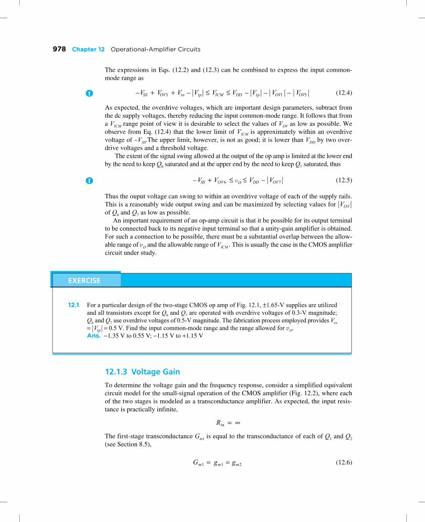
The extent of the signal swing allowed at the output of the op amp is limited at the lower endby the need to keep Q6 saturated and at the upper end by the need to keep Q7 saturated, thus
(12.5)
Thus the ouput voltage can swing to within an overdrive voltage of each of the supply rails.This is a reasonably wide output swing and can be maximized by selecting values for of Q6 and Q7 as low as possible.
An important requirement of an op-amp circuit is that it be possible for its output terminalto be connected back to its negative input terminal so that a unity-gain amplifier is obtained.For such a connection to be possible, there must be a substantial overlap between the allow-able range of vO and the allowable range of VICM . This is usually the case in the CMOS amplifiercircuit under study.
12.1.3 Voltage Gain
To determine the voltage gain and the frequency response, consider a simplified equivalentcircuit model for the small-signal operation of the CMOS amplifier (Fig. 12.2), where eachof the two stages is modeled as a transconductance amplifier. As expected, the input resis-tance is practically infinite,
The first-stage transconductance Gm1 is equal to the transconductance of each of Q1 and Q2
(see Section 8.5),
(12.6)
V– SS VOV3 Vtn Vtp–++ VICM VDD≤ Vtp– VOV1 VOV5––≤
V– SS VOV6+ vO VDD≤ VOV7–≤
VOV
12.1 For a particular design of the two-stage CMOS op amp of Fig. 12.1, ±1.65-V supplies are utilizedand all transistors except for Q6 and Q7 are operated with overdrive voltages of 0.3-V magnitude;Q6 and Q7 use overdrive voltages of 0.5-V magnitude. The fabrication process employed provides Vt n
= = 0.5 V. Find the input common-mode range and the range allowed for vO. Ans. −1.35 V to 0.55 V; −1.15 V to +1.15 V
Vtp
EXERCISE
Rin ∞=
Gm1 gm1 gm2==

12.1 The Two-Stage CMOS Op Amp 979
Since Q1 and Q2 are operated at equal bias currents ( ) and equal overdrive voltages,VOV1 = VOV2,
(12.7)
Resistance R1 represents the output resistance of the first stage, thus
(12.8)
where
(12.9)
and
(12.10)
The dc gain of the first stage is thus
(12.11)
(12.12)
(12.13)
Observe that the magnitude of A1 is increased by operating the differential-pair transistors,Q1 and Q2, at a low overdrive voltage, and by choosing a longer channel length to obtainlarger Early voltages, .
Returning to the equivalent circuit in Fig. 12.2 and leaving the discussion of the variousmodel capacitances until Section 12.1.5, we note that the second-stage transconductance Gm2
is given by
(12.14)
Figure 12.2 Small-signal equivalent circuit for the op amp in Fig. 12.1.
�
�
�
�
Vid Gm1Vid R2 C2
�
Vo
�
C1
�
Vi2
�
Gm2 Vi2R1
CC
I 2⁄
Gm1 2 I 2⁄( )VOV1
-----------------= IVOV1-----------=
R1 ro2 ro4||=
ro2 VA2
I 2⁄-----------=
ro4 VA4
I 2⁄---------=
A1 Gm1R1–=
gm1– ro2 ro4||( )=
2VOV1----------- 1
VA2----------- 1
VA4--------+–=
VA
Gm2 gm62ID6
VOV6-----------= =

980 Chapter 12 Operational-Amplifier Circuits
Resistance R2 represents the output resistance of the second stage, thus
(12.15)
where
(12.16)
and
(12.17)
The voltage gain of the second stage can now be found as
(12.18)
(12.19)
(12.20)
Here again we observe that to increase the magnitude of A2, Q6 has to be operated at a lowoverdrive voltage, and the channel lengths of Q6 and Q7 should be made longer.
The overall dc voltage gain can be found as the product A1A2,
(12.21)
(12.22)
Note that Av is of the order of (gmro)2. Thus the value of Av will be in the range of 500 V/V to
5000 V/V.Finally, we note that the output resistance of the op amp is equal to the output resistance
of the second stage,
(12.23)
Hence Ro can be large (i.e., in the tens-of-kilohms range). Nevertheless, as we learned fromthe study of negative feedback in Chapter 10, application of negative feedback that samplesthe op-amp output voltage results in reducing the ouput resistance by a factor equal to theamount of feedback (1 + Aβ ). Also, as mentioned before, CMOS op amps are rarely requiredto drive heavy resistive loads.
R2 ro6 ro7||=
ro6VA6
ID6--------=
ro7VA7
ID7----------- VA7
ID6-----------= =
A2 Gm2R2–=
gm6 ro6 ro7||( )–=
2VOV6----------- 1
VA6-------- 1
VA7-----------+–=
Av A1A2=
Gm1R1Gm2R2=
gm1 ro2 ro4||( )gm6 ro6 ro7||( )=
Ro ro6 ro7||=

12.1 The Two-Stage CMOS Op Amp 981
12.1.4 Common-Mode Rejection Ratio (CMRR)
The CMRR of the two-stage op amp of Fig. 12.1 is determined by the first stage. This wasanalyzed in Section 8.5.4 and the result is given in Eq. (8.147), namely,
(12.24)
where is the output resistance of the bias current source Observe that CMRR is ofthe order of and thus can be reasonably high. Also, since is proportional to
the CMRR is increased if long channels are used, especially for ,and the transistors are operated at low overdrive voltages.
12.1.5 Frequency Response
Refer to the equivalent circuit in Fig. 12.2. Capacitance C1 is the total capacitance betweenthe output node of the first stage and ground, thus
(12.25)
Capacitance C2 represents the total capacitance between the output node of the op amp andground and includes whatever load capacitance CL that the amplifier is required to drive, thus
(12.26)
Usually, CL is larger than the transistor capacitances, with the result that C2 becomes muchlarger than C1. Finally, note that Cgd6 should be shown in parallel with CC but has beenignored because CC is usually much larger.
The equivalent circuit of Fig. 12.2 was analyzed in detail in Section 9.8.2, where it was foundthat it has two poles and a positive real-axis zero with the following approximate frequencies:
(12.27)
12.2 The CMOS op amp of Fig. 12.1 is fabricated in a process for which = = 20 V/μm. FindA1, A2, and Av if all devices are 1 μm long, VOV1 = 0.2 V, and VOV6 = 0.5 V. Also, find the op-amp outputresistance obtained when the second stage is biased at 0.5 mA.Ans. −100 V/V; −40 V/V; 4000 V/V; 20 kΩ
12.3 If the CMOS op amp in Fig. 12.1 is connected as a unity-gain buffer, show that the closed-loop out-put resistance is given by
VAn′ VAp′
Rout � 1 gm6⁄ gm1 ro2 ro4||( )[ ]
EXERCISES
CMRR gm1 ro2 ro4||( )[ ] 2gm3RSS[ ]=
RSS Q5.gmro( )2 gmro
VA VOV⁄ VA′ L VOV⁄ ,= Q5
C1 Cgd2 Cdb2 Cgd4 Cdb4 Cgs6+ + + +=
C2 Cdb6= Cdb7 Cgd7 CL+ + +
fP1 � 12πR1Gm2R2CC-----------------------------------

982 Chapter 12 Operational-Amplifier Circuits
(12.28)
(12.29)
Here, fP1 is the dominant pole formed by the interaction of Miller-multiplied CC [i.e.,(1 + Gm2R2)CC � Gm2R2CC] and R1. To achieve the goal of a uniform –20-dB/decade gainrolloff down to 0 dB, the unity-gain frequency ft,
(12.30)
(12.31)
must be lower than fP2 and fZ, thus the design must satisfy the following two conditions
(12.32)
and
(12.33)
Simplified Equivalent Circuit The uniform –20-dB/decade gain rolloff obtained at fre-quencies f � fP1 suggests that at these frequencies, the op amp can be represented by the sim-plified equivalent circuit shown in Fig. 12.3. Observe that this attractive simplification isbased on the assumption that the gain of the second stage, , is large, and hence a virtualground appears at the input terminal of the second stage. The second stage then effectivelyacts as an integrator that is fed with the output current signal of the first stage; Gm1Vid.Although derived for the CMOS amplifier, this simplified equivalent circuit is general andapplies to a variety of two-stage op amps, including the first two stages of the 741-type bipolarop amp studied later in this chapter.
Phase Margin The frequency compensation scheme utilized in the two-stage CMOS am-plifier is of the pole-splitting type, studied in Section 10.13.3: It provides a dominant low-frequency pole with frequency fP1 and shifts the second pole beyond ft. Figure 12.4 shows a
fP2 � Gm2
2πC2-------------
fZ � Gm2
2πCC-------------
ft Av fP1=
Gm1
2πCC-------------=
Gm1
CC--------- Gm2
C2---------<
Gm1 Gm2<
A2
��
CC
0 V
Gm1VidVid
�
�
�
�
��
Vo Figure 12.3 An approximate high-frequency equivalent circuit of the two-stage op amp. This circuit applies forfrequencies f � fP1.

12.1 The Two-Stage CMOS Op Amp 983
representative Bode plot for the gain magnitude and phase. Note that at the unity-gain frequencyft, the phase lag exceeds the 90° caused by the dominant pole at fP1. This so-called excess phaseshift is due to the second pole,
(12.34)
and the right-half-plane zero, (12.35)
(12.36)
Thus the phase lag at f = ft will be
(12.37)
and thus the phase margin will be
(12.38)
From our study of the stability of feedback amplifiers in Section 10.12.2, we know that themagnitude of the phase margin significantly affects the closed-loop gain. Therefore, obtain-ing a desired minimum value of phase margin is usually a design requirement.
Figure 12.4 Typical frequency response of the two-stage op amp.
0
0
�
�90º
�180º
fP2 fZ
f (log scale)
f (log scale)
ftfP1
Phase margin
20 log �Av �
20 log �A� (dB)
φP2 tan 1– ftfP2-------⎝ ⎠⎛ ⎞–=
φZ tan 1– ftfZ----⎝ ⎠⎛ ⎞–=
φtotal 90° tan 1– ( ft fP2⁄ ) tan 1– ( ft fZ⁄ )+ +=
Phase margin 180° φtotal–=
90° tan 1– ( ft fP2⁄ )– tan 1– ( ft fZ )⁄–=

984 Chapter 12 Operational-Amplifier Circuits
The problem of the additional phase lag provided by the right-half-plane zero has arather simple and elegant solution: By including a resistance R in series with CC, as shown inFig. 12.5, the transmission zero can be moved to other less-harmful locations. To find thenew location of the transmission zero, set Vo = 0. Then, the current through CC and R will be
, and a node equation at the output yields
Thus the zero is now at
(12.39)
We observe that by selecting we can place the zero at infinite frequency. Aneven better choice would be to select R greater than , thus placing the zero at a nega-tive real-axis location where the phase it introduces adds to the phase margin.
12.1.6 Slew Rate
The slew-rate limitation of op amps is discussed in Chapter 2. Here, we shall illustrate the ori-gin of the slewing phenomenon in the context of the two-stage CMOS amplifier under study.
Figure 12.5 Small-signal equivalent circuit of the op amp in Fig. 12.1 with a resistance R included in serieswith CC.
�
�
�
�
Vid Gm1Vid R2 C2
�
Vo
�
C1
�
Vi2
�
Gm2 Vi2R1
CC R
Vi2 (R 1 sCC )⁄+⁄
Vi2
R 1sCC---------+
------------------- Gm2 Vi2=
s 1 CC1
Gm2--------- R–⎝ ⎠⎛ ⎞=
R 1 Gm2⁄ ,=1 Gm2⁄
12.4 A particular implementation of the CMOS amplifier of Figs. 12.1 and 12.2 provides Gm1 = 1 mA/V,Gm2 = 2 mA/V, ro2 = ro4 = 100 kΩ, ro6 = ro7 = 40 kΩ, and C2 = 1 pF.(a) Find the value of CC that results in f t = 100 MHz. What is the 3-dB frequency of the open-loopgain?(b) Find the value of the resistance R that when placed in series with CC causes the transmissionzero to be located at infinite frequency.(c) Find the frequency of the second pole and hence find the excess phase lag at f = f t, introducedby the second pole, and the resulting phase margin assuming that the situation in (b) pertains.Ans. 1.6 pF; 50 kHz; 500 Ω; 318 MHz; 17.4°; 72.6°
EXERCISE

12.1 The Two-Stage CMOS Op Amp 985
Consider the unity-gain follower of Fig. 12.6 with a step of, say, 1 V applied at the input.Because of the amplifier dynamics, its output will not change in zero time. Thus, immedi-ately after the input is applied, the entire value of the step will appear as a differential signalbetween the two input terminals. In all likelihood, such a large signal will exceed the voltagerequired to turn off one side of the input differential pair ( VOV1: see earlier illustration,Fig. 8.6) and switch the entire bias current I to the other side. Reference to Fig. 12.1 showsthat for our example, Q2 will turn off, and Q1 will conduct the entire current I. Thus Q4 willsink a current I that will be pulled from CC, as shown in Fig. 12.7. Here, as we did inFig. 12.3, we are modeling the second stage as an ideal integrator. We see that the outputvoltage will be a ramp with a slope of :
Thus the slew rate, SR, is given by
(12.40)
It should be pointed out, however, that this is a rather simplified model of the slewing process.
Relationship Between SR and ft A simple relationship exists between the unity-gainbandwidth f t and the slew rate SR. This relationship can be found by combining Eqs. (12.31)
Figure 12.6 A unity-gain follower with a large step input. Since the output voltage cannot change imme-diately, a large differential voltage appears between the op-amp input terminals.
1 V
2
I CC⁄
vo t( ) ICC------ t=
SR ICC------=
��
CC
iD4 � I
I
0
0 V �
�
vo
Figure 12.7 Model of the two-stage CMOSop-amp of Fig. 12.1 when a large differential volt-age is applied.

986 Chapter 12 Operational-Amplifier Circuits
and (12.40) and noting that Gm1 = gm1 = , to obtain
(12.41)
or equivalently,
(12.42)
Thus, for a given ωt, the slew rate is determined by the overdrive voltage at which thefirst-stage transistors are operated. A higher slew rate is obtained by operating Q1 and Q2
at a larger VOV. Now, for a given bias current I, a larger VOV is obtained if Q1 and Q2 are p-channel devices. This is an important reason for using p-channel rather than n-channeldevices in the first stage of the CMOS op amp. Another reason is that it allows the secondstage to employ an n-channel device. Now, since n-channel devices have greater transcon-ductances than corresponding p-channel devices, Gm2 will be high, resulting in a highersecond-pole frequency and a correspondingly higher ωt. However, the price paid for theseimprovements is a lower Gm1 and hence a lower dc gain.
12.1.7 Power-Supply Rejection Ratio (PSRR)
CMOS op amps are usually utilized in what are known as mixed-signal circuits: IC chipsthat combine analog and digital circuits. In such circuits, the switching activity in the digitalportion usually results in increased ripple on the power supplies. A portion of the supply rip-ple can make its way to the op-amp output and thus corrupt the output signal. The traditionalapproach for reducing supply ripple by connecting large capacitances between the supplyrails and ground is not viable in IC design, as such capacitances would consume most of thechip area. Instead, the analog IC designer has to pay attention to another op-amp specifica-tion that so far we have ignored, namely, the power-supply rejection ratio (PSRR).
The PSRR is defined as the ratio of the amplifier differential gain to the gain experiencedby a change in the power-supply voltage ( and ). For circuits utilizing two power sup-plies, we define
(12.42)
and
(12.43)
where
(12.44)
I VOV1⁄
SR 2π ft VOV=
SR VOV ωt=
12.5 Find SR for the CMOS op amp of Fig. 12.1 for the case f t = 100 MHz and VOV1 = 0.2 V. IfCC = 1.6 pF, what must the bias current I be?Ans. 126 V/μs; 200 μA
EXERCISE
vdd vss
PSRR+ Ad
A+------≡
PSRR– Ad
A–--------=
A+ vovdd-------≡

12.1 The Two-Stage CMOS Op Amp 987
(12.45)
Obviously, to minimize the effect of the power-supply ripple, we require the op amp to havea large PSRR.
A detailed analysis of the PSRR of the two-stage CMOS op amp is beyond the scope ofthis book (see Gray et al., 2009). Nevertheless, we make the following brief remarks. It canbe shown that the circuit is remarkably insensitive to variations in , and thus isvery high. This is not the case, however, for the negative-supply ripple , which is coupledto the output primarily through the second-stage transistors and . In particular, the por-tion of that appears at the op-amp output is determined by the voltage divider formed bythe output resistances of and ,
(12.46)
Thus,
(12.47)
Now utilizing from Eq. (12.22) gives
(12.48)
Thus, is of the form and therefore is maximized by selecting long channels L(to increase ), and operating at low .
12.1.8 Design Trade-offs
The performance parameters of the two-stage CMOS amplifier are primarily determined bytwo design parameters:
1. The length L used for the channel of each MOSFET.
2. The overdrive voltage at which each transistor is operated.
Throughout this section, we have found that a larger L and correspondingly larger increases the amplifier gain, CMRR and PSRR. We also found that operating at a lower
increases these three parameters as well as increasing the input common-mode rangeand the allowable range of output swing. Also, although we have not analyzed the offsetvoltage of the op amp here, we know from our study of the subject in Section 8.4.1 that anumber of the components of the input offset voltage that arises from random device mis-matches are proportional to at which the MOSFETs of the input differential pair areoperated. Thus the offset is minimized by operating at a lower .
There is, however, an important MOSFET performance parameter that requires the selec-tion of a larger , namely, the transition frequency , which determines the high-fre-quency performance of the MOSFET,
(12.49)
A– vo
vss------=
VDD PSRR+
vssQ6 Q7
vssQ6 Q7
vo vssro7
ro6 ro7+--------------------=
A– vo
vss------ ro7
ro6 ro7+--------------------=≡
Ad
PSRR– Ad
A–-------- gm1 ro2 ro4||( )gm6ro6=≡
PSRR– gmro( )2
VA VOV
VOV
VA
VOV
VOVVOV
VOV fT
fTgm
2π Cgs Cgd+( )-----------------------------------=

988 Chapter 12 Operational-Amplifier Circuits
For an n-channel MOSFET, we can show that (see Appendix 7.A)
(12.50)
A similar relationship applies for the PMOS transistor, with and replacing and, respectively. Thus to increase and improve the high-frequency response of the op
amp, we need to use a larger overdrive value and, not surprisingly, shorter channels. Alarger also results in a higher op-amp slew rate SR (Eq. 12.41). Finally, note that theselection of a larger results, for the same bias current, in a smaller W/L, which com-bined with a short L leads to smaller devices and hence lower values of MOSFET capaci-tances and higher frequencies of operation.
In conclusion, the selection of presents the designer with a trade-off betweenimproving the low-frequency performance parameters on the one hand and the high-fre-quency performance on the other. For modern submicron technologies, which require opera-tion from power supplies of 1 V to 1.5 V, overdrive voltages between 0.1 V and 0.3 V aretypically utilized. For these process technologies, analog designers typically use channellengths that are at least 1.5 to 2 times the specified value of , and even longer channelsare used for current-source bias transistors.
fT � 1.5μnVOV
2π L2-----------------------
μp VOV μnVOV fT
VOVVOV
VOV
Lmin
We conclude our study of the two-stage CMOS op amp with a design example. Let it be required todesign the circuit to obtain a dc gain of 4000 V/V. Assume that the available fabrication technology is ofthe 0.5-μm type for which Vt n = = 0.5 V, = 200 μA/V2, = 80 μA/V2, = = 20 V/μm,and VDD = VSS = 1.65 V. To achieve a reasonable dc gain per stage, use L = 1 μm for all devices. Also, forsimplicity, operate all devices at the same , in the range of 0.2 V to 0.4 V. Use I = 200 μA, and toobtain a higher Gm2, and hence a higher fP2, use ID6 = 0.5 mA. Specify the ratios for all transistors.Also give the values realized for the input common-mode range, the maximum possible output swing, Rinand Ro. Also determine the CMRR and PSRR realized. If C1 = 0.2 pF and C2 = 0.8 pF, find the requiredvalues of CC and the series resistance R to place the transmission zero at s = ∞ and to obtain the highestpossible ft consistent with a phase margin of 75°. Evaluate the values obtained for ft and SR.
Solution
Using the voltage-gain expression in Eq. (12.22),
To obtain Av = 4000, given VA = 20 V,
Vtp kn′ kp′ VAn′ VAp′
VOVW L⁄
Av gm1 ro2 ro4||( )gm6 ro6 ro7||( )=
2 I 2⁄( )VOV
----------------- 12---×
VA
I 2⁄( )-------------
2ID6
VOV----------×× 1
2---
VA
ID6-------××=
VA
VOV---------⎝ ⎠⎛ ⎞
2=
4000 400VOV
2---------=
Example 12.1

12.1 The Two-Stage CMOS Op Amp 989
To obtain the required ( ) ratios of Q1 and Q2,
Thus,
and
For Q3 and Q4 we write
to obtain
For Q5,
Thus,
Since Q7 is required to conduct 500 μA, its ( ) ratio should be 2.5 times that of Q5,
For Q6 we write
Thus,
VOV 0.316 V=
W L⁄
ID112--- kp′
WL-----⎝ ⎠⎛ ⎞
1VOV
2=
100 12--- 80 W
L-----⎝ ⎠⎛ ⎞×
10.3162×=
WL-----⎝ ⎠⎛ ⎞
1
25 μm1 μm----------------=
WL-----⎝ ⎠⎛ ⎞
2
25 μm1 μm----------------=
100 12--- 200 W
L-----⎝ ⎠⎛ ⎞
30.3162××=
WL-----⎝ ⎠⎛ ⎞
3
WL-----⎝ ⎠⎛ ⎞
4
10 μm1 μm
----------------= =
200 12--- 80 W
L-----⎝ ⎠⎛ ⎞
50.3162××=
WL-----⎝ ⎠⎛ ⎞
5
50 μm1 μm----------------=
W L⁄
WL-----⎝ ⎠⎛ ⎞
72.5 W
L-----⎝ ⎠⎛ ⎞
5
125 μm1 μm
-------------------= =
500 12--- 200 W
L-----⎝ ⎠⎛ ⎞
60.3162×××=
WL-----⎝ ⎠⎛ ⎞
6
50 μm1 μm----------------=

990 Chapter 12 Operational-Amplifier Circuits
Example 12.1 continued
Finally, let’s select thus
The input common-mode range can be found using the expression in Eq. (12.4) as
The maximum signal swing allowable at the output is found using the expression in Eq. (12.5) as
The input resistance is practically infinite, and the output resistance is
The CMRR is determined using Eq. (12.24),
where . Thus,
Expressed in decibels, we have
dB
The PSRR is determined using Eq. (12.48):
or, expressed in decibels,
dB
To determine fP2 we use Eq. (12.28) and substitute for Gm2,
Thus,
IREF 20 μA,=
WL-----⎝ ⎠⎛ ⎞
80.1 W
L-----⎝ ⎠⎛ ⎞
5
5 μm1 μm-------------= =
1.33– V VICM 0.52 V≤ ≤
1.33– V vO 1.33 V≤ ≤
Ro ro6= ro7|| 12--- 20
0.5-------× 20 kΩ= =
CMRR gm1 ro2 ro4||( ) 2gm3RSS( )=
RSS ro5 VA ⁄ I==
CMRR 2 I 2⁄( )VOV
----------------- 12---
VA
I 2⁄( )-------------×× 2 2 I 2⁄( )
VOV-----------------××
VA
I------×=
2VA
VOV---------⎝ ⎠⎛ ⎞
22 20
0.316-------------⎝ ⎠⎛ ⎞
28000===
CMRR 20 log 8000 78==
PSRR gm1 ro2 ro4||( )gm6ro6=
2 I 2⁄( )VOV
----------------- 12---
VA
I 2⁄( )-------------××
2ID6
VOV----------×
VA
ID6-------×=
2VA
VOV---------⎝ ⎠⎛ ⎞
22 20
0.316-------------⎝ ⎠⎛ ⎞
28000===
PSRR 20 log 8000 78==
Gm2 gm62ID6
VOV---------- 2 0.5×
0.316---------------- 3.2 mA/V= = = =
fP23.2 10 3–×
2π 0.8× 10 12–×---------------------------------------- 637 MHz= =

12.2 The Folded-Cascode CMOS Op Amp 991
12.2 The Folded-Cascode CMOS Op Amp
In this section we study another type of CMOS op-amp circuit: the folded cascode. The cir-cuit is based on the folded-cascode amplifier studied in Section 7.3.6. There, it was men-tioned that although composed of a CS transistor and a CG transistor of opposite polarity,the folded-cascode configuration is generally considered to be a single-stage amplifier. Sim-ilarly, the op-amp circuit that is based on the cascode configuration is considered to be asingle-stage op amp. Nevertheless, it can be designed to provide performance parametersthat equal and in some respects exceed those of the two-stage topology studied in thepreceding section. Indeed, the folded-cascode op-amp topology is currently as popular as thetwo-stage structure. Furthermore, the folded-cascode configuration can be used in conjunctionwith the two-stage structure to provide performance levels higher than those available fromeither circuit alone.
12.2.1 The Circuit
Figure 12.8 shows the structure of the CMOS folded-cascode op amp. Here, Q1 and Q2 formthe input differential pair, and Q3 and Q4 are the cascode transistors. Recall that for
To move the transmission zero to we select the value of R as
For a phase margin of 75°, the phase shift due to the second pole at must be 15°, that is,
Thus,
The value of CC can be found using Eq. (12.31),
where
Thus,
The value of SR can now be found using Eq. (12.41) as
s ∞,=
R 1Gm2--------- 1
3.2 10 3–×------------------------ 316 Ω= = =
f = ft
tan 1– ftfP2------ 15°=
ft 637 tan 15°× 171 MHz= =
CCGm1
2π ft----------=
Gm1 gm12 100 μA×
0.316 V---------------------------- 0.63 mA/V= = =
CC10.63 10 3–×
2π 171× 106×------------------------------------ 0.6 pF= =
SR 2π 171× 106 0.316××=
340 V/μs=

992 Chapter 12 Operational-Amplifier Circuits
differential input signals, each of Q1 and Q2 acts as a common-source amplifier. Also notethat the gate terminals of Q3 and Q4 are connected to a constant dc voltage (VBIAS1) and henceare at signal ground. Thus, for differential input signals, each of the transistor pairs Q1–Q3
and Q2–Q4 acts as a folded-cascode amplifier, such as the one in Fig. 7.16. Note that theinput differential pair is biased by a constant-current source I. Thus each of Q1 and Q2 isoperating at a bias current . A node equation at each of their drains shows that the biascurrent of each of Q3 and Q4 is Selecting forces all transistors to operateat the same bias current of For reasons that will be explained shortly, however, thevalue of IB is usually made somewhat greater than I.
As we learned in Chapter 7, if the full advantage of the high output-resistance achievedthrough cascoding is to be realized, the output resistance of the current-source load must beequally high. This is the reason for using the cascode current mirror Q5 to Q8, in the circuitof Fig. 12.8. (This current-mirror circuit was studied in Section 7.5.1.) Finally, note thatcapacitance CL denotes the total capacitance at the output node. It includes the internal tran-sistor capacitances, an actual load capacitance (if any), and possibly an additional capacitancedeliberately introduced for the purpose of frequency compensation. In many cases, however,the load capacitance will be sufficiently large, obviating the need to provide additionalcapacitance to achieve the desired frequency compensation. This topic will be discussedshortly. For the time being, we note that unlike the two-stage circuit, that requires theintroduction of a separate compensation capacitor CC, here the load capacitance contributesto frequency compensation.
A more complete circuit for the CMOS folded-cascode op amp is shown in Fig. 12.9.Here we show the two transistors Q9 and Q10, which provide the constant bias currents IB,and transistor Q11, which provides the constant current I utilized for biasing the differentialpair. Observe that the details for generating the bias voltages VBIAS1, VBIAS2, and VBIAS3 are not
Figure 12.8 Structure of the folded-cascode CMOS op amp.
Q1 Q2
Q3
Q5
Q7
Q4
Q6
Q8
IB IB
I
VDD
�VSS
� �
VBIAS1
Input differentialpair
Cascode transistors
Cascode currentmirror
CL
vo
I 2⁄IB I 2⁄–( ). IB = I
I 2⁄ .

12.2 The Folded-Cascode CMOS Op Amp 993
shown. Nevertheless, we are interested in how the values of these voltages are to be selected.Toward that end, we evaluate the input common-mode range and the allowable output swing.
12.2.2 Input Common-Mode Range and Output Swing
To find the input common-mode range, let the two input terminals be tied together and con-nected to a voltage VICM . The maximum value of VICM is limited by the requirement that Q1 andQ2 operate in saturation at all times. Thus VICMmax should be at most Vtn volts above the voltageat the drains of Q1 and Q2. The latter voltage is determined by VBIAS1 and must allow for a volt-age drop across Q9 and Q10 at least equal to their overdrive voltage, = Assumingthat Q9 and Q10 are indeed operated at the edge of saturation, VICMmax will be
(12.51)
which can be larger than VDD, a significant improvement over the case of the two-stage cir-cuit. The value of VBIAS2 should be selected to yield the required value of IB while operatingQ9 and Q10 at a small value of (e.g., 0.2 V or so). The minimum value of VICM can beobtained as
(12.52)
The presence of the threshold voltage Vt n in this expression indicates that VICMmin is not suffi-ciently low. Later in this section we shall describe an ingenious technique for solving thisproblem. For the time being, note that the value of VBIAS3 should be selected to provide the
Figure 12.9 A more complete circuit for the folded-cascode CMOS amplifier of Fig. 12.8.
Q1 Q2
Q3
Q5
Q9
Q7
Q4
Q6
Ro6
Ro4
Q8
VBIAS3
�VSS
VDD
VBIAS2
Q11
Q10
� �
VBIAS1
CL
vO
VOV9 VOV10 .
VICMmax VDD VOV9 Vtn+–=
VOV
VICMmin VSS VOV11 VOV1 Vtn+ + +–=

994 Chapter 12 Operational-Amplifier Circuits
required value of I while operating Q11 at a low overdrive voltage. Combining Eqs. (12.51)and (12.52) provides
(12.53)
The upper end of the allowable range of vO is determined by the need to maintain Q10 and Q4
in saturation. Note that Q10 will operate in saturation as long as an overdrive voltage, appears across it. It follows that to maximize the allowable positive swing of vO (and VICMmax),we should select the value of VBIAS1 so that Q10 operates at the edge of saturation, that is,
(12.54)
The upper limit of vO will then be
(12.55)
which is two overdrive voltages below VDD. The situation is not as good, however, at theother end: Since the voltage at the gate of Q6 is −VSS + VGS7 + VGS5 or equivalently −VSS + VOV7
+ VOV5 + 2Vtn, the lowest possible vO is obtained when Q6 reaches the edge of saturation,namely, when vO decreases below the voltage at the gate of Q6 by Vtn, that is,
(12.56)
Note that this value is two overdrive voltages plus a threshold voltage above . This is adrawback of utilizing the cascode mirror. The problem can be alleviated by using a modifiedmirror circuit, as we shall shortly see.
12.2.3 Voltage Gain
The folded-cascode op amp is simply a transconductance amplifier with an infinite inputresistance, a transconductance Gm and an output resistance Ro. Gm is equal to gm of each ofthe two transistors of the differential pair,
(12.57)
Thus,
(12.58)
VSS VOV11 VOV1 Vtn VICM VDD VOV9 Vtn+–≤ ≤+ + +–
VOV10 ,
VBIAS1 VDD VOV10 VSG 4––=
vOmax VDD VOV10– VOV4–=
vOmin −VSS VOV7 VOV5 Vt n+ + +=
V– SS
12.6 For a particular design of the folded-cascode op amp of Fig. 12.9, ±1.65-V supplies are utilized andall transistors are operated at overdrive voltages of 0.3-V magnitude. The fabrication processemployed provides Find the input common-mode range and the range al-lowed for vO.Ans. −0.55 V to +1.85 V; −0.55 V to +1.05 V.
Vtn = Vtp = 0.5 V.
EXERCISE
Gm gm1 gm2= =
Gm2 I 2⁄( )
VOV1----------------- I
VOV1-----------= =

12.2 The Folded-Cascode CMOS Op Amp 995
The output resistance Ro is the parallel equivalent of the output resistance of the cascodeamplifier and the output resistance of the cascode mirror, thus
(12.59)
Reference to Fig. 12.9 shows that the resistance Ro4 is the output resistance of the CG tran-sistor Q4. The latter has a resistance in its source lead, thus
(12.60)
The resistance Ro6 is the output resistance of the cascode mirror and is thus given byEq. (7.25), thus
(12.61)
Combining Eqs. (12.59) to (12.61) gives
(12.62)
The dc open-loop gain can now be found using Gm and Ro, as
(12.63)
Thus,
(12.64)
Figure 12.10 shows the equivalent-circuit model including the load capacitance CL, whichwe shall take into account shortly.
Because the folded-cascode op amp is a transconductance amplifier, it has been giventhe name operational transconductance amplifier (OTA). Its very high output resistance,which is of the order of (see Eq. 12.62) is what makes it possible to realize a relativelyhigh voltage gain in a single amplifier stage. However, such a high output resistance may bea cause of concern to the reader; after all, in Chapter 2, we stated that an ideal op amp has azero output resistance! To alleviate this concern somewhat, let us find the closed-loop out-put resistance of a unity-gain follower formed by connecting the output terminal of the cir-cuit of Fig. 12.9 back to the negative input terminal. Since this feedback is of the voltagesampling type, it reduces the output resistance by the factor , where and
that is,
(12.65)
Ro Ro4 Ro6||=
ro2 ro10||( )
Ro4 � gm4ro4( ) ro2 ro10||( )
Ro6 � gm6ro6ro8
Ro gm4ro4 ro2 ro10||( )[ ] gm6ro6ro8( )||=
Av GmRo=
Av gm1 gm4ro4 ro2 ro10||( )[ ] gm6ro6ro8( )||{ }=
gmro2
1 Aβ+( ) A Av=β 1,=
RofRo
1 Av+--------------- �
Ro
Av-----=
GmVid CLRo
Vid
�
�
�
�
Vo
Figure 12.10 Small-signal equivalent cir-cuit of the folded-cascode CMOS amplifier.Note that this circuit is in effect an opera-tional transconductance amplifier (OTA).

996 Chapter 12 Operational-Amplifier Circuits
Substituting for Av from Eq. (12.63) gives
(12.66)
which is a general result that applies to any OTA to which 100% voltage feedback isapplied. For our particular circuit, , thus
(12.67)
Since gm1 is of the order of 1 mA/V, Rof will be of the order of 1 kΩ . Although this is notvery small, it is reasonable in view of the simplicity of the op-amp circuit as well as the factthat this type of op amp is not usually intended to drive low-valued resistive loads.
12.2.4 Frequency Response
From Section 9.6, we know that one of the advantages of the cascode configuration is itsexcellent high-frequency response. It has poles at the input, at the connection between theCS and CG transistors (i.e., at the source terminals of Q3 and Q4), and at the output terminal.Normally, the first two poles are at very high frequencies, especially when the resistance ofthe signal generator that feeds the differential pair is small. Since the primary purpose ofCMOS op amps is to feed capacitive loads, CL is usually large, and the pole at the outputbecomes dominant. Even if CL is not large, we can increase it deliberately to give the op ampa dominant pole. From Fig. 12.10 we can write
(12.68)
Thus, the dominant pole has a frequency f P,
(12.69)
and the unity-gain frequency f t will be
(12.70)
From a design point of view, the value of CL should be such that at f = f t the excess phaseresulting from the nondominant poles is small enough to permit the required phase margin tobe achieved. If CL is not large enough to achieve this purpose, it can be augmented.
Rof � 1Gm-------
Gm gm1=
Rof 1 gm1⁄=
12.7 The CMOS op amp of Figs. 12.8 and 12.9 is fabricated in a process for which = = 20V/μm. If all devices have 1-μm channel length and are operated at equal overdrive voltages of0.2-V magnitude, find the voltage gain obtained. If each of Q1 to Q8 is biased at 100 μA, what valueof Ro is obtained?Ans. 13,333 V/V; 13.3 MΩ
VAn′ VAp′
EXERCISE
Vo
Vid------- GmRo
1 sCLRo+------------------------=
fP1
2πCLRo-------------------=
ft GmRo fPGm
2πCL-------------= =

12.2 The Folded-Cascode CMOS Op Amp 997
It is important to note the different effects of increasing the load capacitance on the oper-ation of the two op-amp circuits we have studied. In the two-stage circuit, if CL is increased,the frequency of the second pole decreases, the excess phase shift at f = f t increases, and thephase margin is reduced. Here, on the other hand, when CL is increased, f t decreases, butthe phase margin increases. In other words, a heavier capacitive load decreases the bandwidthof the folded-cascode amplifier but does not impair its response (which happens when thephase margin decreases). Of course, if an increase in CL is anticipated in the two-stage
case, the designer can increase CC, thus decreasing f t and restoring the phase marginto its required value.
12.2.5 Slew Rate
As discussed in Section 12.1.6, slewing occurs when a large differential input signal isapplied. Refer to Fig. 12.8 and consider the case of a large signal Vid applied so that Q2 cutsoff and Q1 conducts the entire bias current I. We see that Q3 will now carry a current
, and Q4 will conduct a current IB. The current mirror will see an input currentof through Q5 and Q7 and thus its output current in the drain of Q6 will be It follows that at the output node the current that will flow into CL will be I4 − I6 = IB −
Thus the output vO will be a ramp with a slope of which is the slew rate,
(12.71)
Note that the reason for selecting is to avoid turning off the current mirror com-pletely; if the current mirror turns off, the output distortion increases. Typically, IB is set10% to 20% larger than I. Finally, Eqs. (12.70), (12.71), and (12.58) can be combined toobtain the following relationship between SR and f t
(12.72)
which is identical to the corresponding relationship in the case of the two-stage design.Note, however, that this relationship applies only when
op-amp
IB I–( )IB I–( ) IB I–( ).
IB I–( ) I.= I CL⁄
SR ICL------=
IB I>
SR 2πft VOV1=
IB I.>
Consider a design of the folded-cascode op amp of Fig. 12.9 for which I = 200 μA, IB = 250 μA, and for all transistors is 0.25 V. Assume that the fabrication process provides = 100 = 40
, and Let all transistors have and assume that Find ID, gm, ro, and W/L for all transistors. Find the allowable range of and of the output voltage swing. Determine the values of Av, f t, fP, and SR. What is the power dissipationof the op amp?
Solution
From the given values of I and IB we can determine the drain current ID for each transistor. The transcon-ductance of each device is found using
VOV kn′ μA/V2, kp′μA/V2 V ′A = 20 V/μm. VDD = VSS = 2.5 V, Vt 0.75 V.= L = 1 μm
CL = 5 pF. VICM
gm2ID
VOV---------
2ID
0.25----------= =
Example 12.2

998 Chapter 12 Operational-Amplifier Circuits
Example 12.2 continued
and the output resistance ro from
The W/L ratio for each transistor is determined from
The results are as follows:
Note that for all transistors,
Using the expression in Eq. (12.53), the input common-mode range is found to be
The output voltage swing is found using Eqs. (12.55) and (12.56) to be
To obtain the voltage gain, we first determine Ro4 using Eq. (12.60) as
and Ro6 using Eq. (12.61) as
The output resistance Ro can then be found as
and the voltage gain
The unity-gain bandwidth is found using Eq. (12.70),
Thus, the dominant-pole frequency must be
Q1 Q2 Q3 Q4 Q5 Q6 Q7 Q8 Q9 Q10 Q11
ID (μA) 100 100 150 150 150 150 150 150 250 250 200gm (mA/V) 0.8 0.8 1.2 1.2 1.2 1.2 1.2 1.2 2.0 2.0 1.6ro (kΩ) 200 200 133 133 133 133 133 133 80 80 100W/L 32 32 120 120 48 48 48 48 200 200 64
roVA
ID--------- 20
ID------= =
WL-----⎝ ⎠⎛ ⎞
i
2IDi
k′V2OV
----------------=
gmro 160 V/V=
VGS 1.0 V=
1.25– V VICM 3 V≤ ≤
1.25– V vO 2 V≤ ≤
Ro4 160 200 80||( ) 9.14 MΩ= =
Ro6 21.28 MΩ=
Ro Ro4 Ro6|| 6.4 MΩ= =
Av GmRo 0.8 10 3– 6.4× 10⁶××= =
5120 V/V=
ft0.8 10 3–×
2π 5× 10 12–×----------------------------------- 25.5 MHz= =
fPftAv----- 25.5 MHz
5120------------------------- 5 kHz= = =

12.2 The Folded-Cascode CMOS Op Amp 999
12.2.6 Increasing the Input Common-Mode Range: Rail-to-Rail Input Operation
In Section 12.2.2 we found that while the upper limit on the input common-mode rangeexceeds the supply voltage VDD, the magnitude of lower limit is significantly lower than VSS.The opposite situation occurs if the input differential amplifier is made up of PMOS transis-tors. It follows that an NMOS and a PMOS differential pair placed in parallel would providean input stage with a common-mode range that exceeds the power supply voltage in bothdirections. This is known as rail-to-rail input operation. Figure 12.11 shows such an arrange-ment. To keep the diagram simple, we have not shown the parallel connection of the two dif-ferential pairs: The two positive-input terminals are to be connected together and the twonegative-input terminals are to be tied together. Transistors Q5 and Q6 are the cascode tran-sistors for the Q1–Q2 pair, and transistors Q7 and Q8 are the cascode devices for the Q3–Q4
pair. The output voltage Vo is shown taken differentially between the drains of the cascodedevices. To obtain a single-ended output, a differential-to-single-ended conversion circuitshould be connected in cascade.
Figure 12.11 indicates by arrows the direction of the current increments that result fromthe application of a positive differential input signal Vi d. Each of the current increments indi-cated is equal to Gm(Vid ⁄ 2) where Gm = gm1 = gm2 = gm3 = gm4. Thus the total current feedingeach of the two output nodes will be GmVid. Now, if the output resistance between each of thetwo nodes and ground is denoted Ro, the output voltage will be
(12.73)
Thus the voltage gain will be
(12.74)
This, however, assumes that both differential pairs will be operating simultaneously. This inturn occurs only over a limited range of VICM . Over the remainder of the input common-mode range, only one of the two differential pairs will be operational, and the gain drops tohalf of the value in Eq. (12.74). This rail-to-rail, folded-cascode structure is utilized in acommercially available op amp.1
1The Texas Instruments OPA357.
The slew rate can be determined using Eq. (12.71),
Finally, to determine the power dissipation we note that the total current is 500 μA = 0.5 mA, and the totalsupply voltage is 5 V, thus
SR ICL------ 200 10 6–×
5 10 12–×------------------------- 40 V/μs= = =
PD 5 0.5× 2.5 mW= =
Vo 2GmRoVid=
Av 2GmRo=

1000 Chapter 12 Operational-Amplifier Circuits
12.2.7 Increasing the Output Voltage Range: The Wide-Swing Current Mirror
In Section 12.2.2 it was found that while the output voltage of the circuit of Fig. 12.9 canswing to within of VDD, the cascode current mirror limits the negative swing to
above −VSS. In other words, the cascode mirror reduces the voltage swing byVt volts. This point is further illustrated in Fig. 12.12(a), which shows a cascode mirror (withVSS = 0, for simplicity) and indicates the voltages that result at the various nodes. Observe
Figure 12.11 A folded-cascode op amp that employs two parallel complementary input stages to achieverail-to-rail input common-mode operation. Note that the two “+” terminals are connected together and thetwo “–” terminals are connected together.
Q1 Q2
Q5
Q7
Q6
Q4 Q3Q8
Vo
VBIAS1
IB IB
I
VDD
�VSS
IB
I
IB
� �
��
VBIAS2
� �
12.8 For the circuit in Fig. 12.11, assume that all transistors, including those that implement the currentsources, are operating at equal overdrive voltages of 0.3-V magnitude and have andthat (a) Find the range over which the NMOS input stage operates.(b) Find the range over which the PMOS input stage operates.(c) Find the range over which both operate (the overlap range).(d) Find the input common-mode range.(Note that to operate properly, each of the current sources requires a minimum voltage of across its terminals.)Ans. −1.2 V to +2.9 V; −2.9 V to +1.2 V, −1.2 V to +1.2 V; −2.9 V to +2.9 V
Vt 0.7 V=VDD VSS 2.5 V.= =
VOV
EXERCISE
2 VOV2 VOV Vt+[ ]

12.2 The Folded-Cascode CMOS Op Amp 1001
that because the voltage at the gate of Q3 is , the minimum voltage permitted atthe output (while Q3 remains saturated) is Vt + 2VOV, hence the extra Vt. Also, observe that Q1
is operating with a drain-to-source voltage Vt + VOV, which is Vt volts greater than it needs tooperate in saturation.
The observations above lead us to the conclusion that to permit the output voltage at thedrain of Q3 to swing as low as 2VOV, we must lower the voltage at the gate of Q3 from 2Vt +2VOV to Vt + 2VOV. This is exactly what is done in the modified mirror circuit in Fig.12.12(b): The gate of Q3 is now connected to a bias voltage VBIAS = Vt + 2VOV. Thus the out-put voltage can go down to 2VOV with Q3 still in saturation. Also, the voltage at the drain ofQ1 is now VOV and thus Q1 is operating at the edge of saturation. The same is true of Q2 andthus the current tracking between Q1 and Q2 will be assured. Note, however, that we can nolonger connect the gate of Q2 to its drain. Rather, it is connected to the drain of Q4. Thisestablishes a voltage of Vt + VOV at the drain of Q4 which is sufficient to operate Q4 in satura-tion (as long as Vt is greater than VOV, which is usually the case). This circuit is known as thewide-swing current mirror. Finally, note that Fig. 12.12(b) does not show the circuit forgenerating VBIAS. There are a number of possible circuits to accomplish this task, one ofwhich is explored in Exercise 12.9.
Q4
Q2
Q3
Q1
IREF IO
Vt � VOV
2Vt � 2VOV
Vt � VOV
(a)
Q4
Q2
Q3
Q1
IREF IO
VOVVOV
Vt � VOV
VBIAS � Vt � 2VOV
Vt � VOV
(b)
Figure 12.12 (a) Cascode current mirror with the voltages at all nodes indicated. Note that the minimumvoltage allowed at the output is Vt + 2VOV . (b) A modification of the cascode mirror that results in the reduc-tion of the minimum output voltage to VOV. This is the wide-swing current mirror. The circuit requires a biasvoltage VBIAS.
2Vt 2VOV+
12.9 Show that if transistor Q5 in the circuit of Fig. E12.9 has a W/L ratio equal to one-quarter that of thetransistors in the wide-swing current mirror of Fig. 12.12(b), and provided the same value of IREF isutilized in both circuits, then the voltage generated, V5 is Vt + 2VOV, which is the value of VBIAS need-ed for the gates of Q3 and Q4.
EXERCISE

1002 Chapter 12 Operational-Amplifier Circuits
12.3 The 741 Op-Amp Circuit
Our study of BJT op amps is in two parts: The first part (Sections 12.3–12.6) is focused on the741 op-amp circuit, which is shown in Fig. 12.13; the second part (Section 12.7) presents someof the more recent design techniques. Note that in keeping with the IC design philosophy,the circuit in Fig. 12.13 uses a large number of transistors, but relatively few resistors, andonly one capacitor. This philosophy is dictated by the economics (silicon area, ease of fabri-cation, quality of realizable components) of the fabrication of active and passive compo-nents in IC form (see Section 7.1 and Appendix A).
As is the case with most general-purpose IC op amps, the 741 requires two power supplies, and . Normally, but the circuit also operates satisfactorily
with the power supplies reduced to much lower values (such as ±5 V). It is important toobserve that no circuit node is connected to ground, the common terminal of the two supplies.
With a relatively large circuit such as that shown in Fig. 12.13, the first step in the analy-sis is the identification of its recognizable parts and their functions. This can be done asfollows.
12.3.1 Bias Circuit
The reference bias current of the 741 circuit, IREF, is generated in the branch at the extremeleft of Fig. 12.13, consisting of the two diode-connected transistors Q11 and Q12 and theresistance R5. Using a Widlar current source formed by Q11, Q10, and R4, bias current for thefirst stage is generated in the collector of Q10. Another current mirror formed by Q8 and Q9
takes part in biasing the first stage.The reference bias current IREF is used to provide two proportional currents in the
collectors of Q13. This double-collector lateral 2 pnp transistor can be thought of as twotransistors whose base–emitter junctions are connected in parallel. Thus Q12 and Q13 forma two-output current mirror: One output, the collector of Q13B, provides bias current andacts as a current-source load for Q17, and the other output, the collector of Q13A, providesbias current for the output stage of the op amp.
2See Appendix A for a description of lateral pnp transistors. Also, their characteristics were discussed in the Appendix to Chapter 7, Section 7.A.2.
IREF
Q5
V5
Figure E12.9
+VCC VEE– VCC = VEE = 15 V,

12.3 The 741 Op-Amp Circuit 1003
Figu
re 1
2.13
The
741
op-a
mp
circ
uit:
Q11
, Q12
, and
R5 g
ener
ate
a re
fere
nce
bias
cur
rent
; IR
EF. Q
10, Q
9, an
d Q
8 bia
s th
e in
put s
tage
, whi
ch is
com
pose
d of
Q1 t
o Q
7.Th
e se
cond
gai
n st
age
is c
ompo
sed
of Q
16 a
nd Q
17 w
ith Q
13B a
ctin
g as
act
ive
load
. The
cla
ss A
B o
utpu
t sta
ge is
form
ed b
y Q
14 a
nd Q
20 w
ith b
iasi
ng d
evic
es Q
13A,
Q18
,an
d Q
19, a
nd a
n in
put b
uffe
r Q23
. Tra
nsis
tors
Q15
, Q21
, Q24
, and
Q22
serv
e to
pro
tect
the
ampl
ifier
aga
inst
out
put s
hort
circ
uits
and
are
nor
mal
ly c
ut o
ff.

1004 Chapter 12 Operational-Amplifier Circuits
Two more transistors, Q18 and Q19, take part in the dc bias process. The purpose of Q18
and Q19 is to establish two VBE drops between the bases of the output transistors Q14 and Q20.
12.3.2 Short-Circuit Protection Circuitry
The 741 circuit includes a number of transistors that are normally off and conduct only inthe event of on attempt to draw a large current from the op-amp output terminal. This hap-pens, for example, if the output terminal is short-circuited to one of the two supplies. Theshort-circuit protection network consists of R6, R7, Q15, Q21, Q24, R11, and Q22. In the follow-ing we shall assume that these transistors are off. Operation of the short-circuit protectionnetwork will be explained in Section 12.5.3.
12.3.3 The Input Stage
The 741 circuit consists of three stages: an input differential stage, an intermediate single-ended high-gain stage, and an output-buffering stage. The input stage consists of transistorsQ1 through Q7, with biasing performed by Q8, Q9, and Q10. Transistors Q1 and Q2 act as emit-ter followers, causing the input resistance to be high and delivering the differential input sig-nal to the differential common-base amplifier formed by Q3 and Q4. Thus the input stage isthe differential version of the common-collector common-base configuration discussed inSection 7.6.3.
Transistors Q5, Q6, and Q7 and resistors R1, R2, and R3 form the load circuit of the inputstage. This is an elaborate current-mirror load circuit, which we will analyze in detail in Section12.5.1. The circuit is based on the base-current-compensated mirror studied in Section 7.5, but itincludes two emitter-degeneration resistors R1 and R2, and a large resistor R3 in the emitter of Q7.It will be shown that this load circuit not only provides a high-resistance load but also convertsthe signal from differential to single-ended form with no loss in gain or common-mode rejec-tion. The output of the input stage is taken single-endedly at the collector of Q6.
As mentioned in Section 8.6.2, every op-amp circuit includes a level shifter whose func-tion is to shift the dc level of the signal so that the signal at the op-amp output can swingpositive and negative. In the 741, level shifting is done in the first stage using the lateral pnptransistors Q3 and Q4. Although lateral pnp transistors have poor high-frequency perfor-mance, their use in the common-base configuration (which is known to have good high-frequency response) does not seriously impair the op-amp frequency response.
The use of the lateral pnp transistors Q3 and Q4 in the first stage results in an added advan-tage: protection of the input-stage transistors Q1 and Q2 against emitter–base junction break-down. Since the emitter–base junction of an npn transistor breaks down at about 7 V of reversebias (see Section 6.9.1), regular npn differential stages suffer such a breakdown if, say, thesupply voltage is accidentally connected between the input terminals. Lateral pnp transistors,however, have high emitter–base breakdown voltages (about 50 V); and because they are con-nected in series with Q1 and Q2, they provide protection of the 741 input transistors, Q1 and Q2.
Finally, note that except for using input buffer transistors, the 741 input stage is essen-tially a current-mirror-loaded differential amplifier. It is quite similar to the input stage ofthe CMOS amplifier in Fig. 12.1.
12.3.4 The Second Stage
The second or intermediate stage is composed of Q16, Q17, Q13B, and the two resistors R8 and R9.Transistor Q16 acts as an emitter follower, thus giving the second stage a high input

12.3 The 741 Op-Amp Circuit 1005
resistance. This minimizes the loading on the input stage and avoids loss of gain. Also,adding Q16 with its 50-kΩ emitter resistance (which is similar to Q7 and R3) increases thesymmetry of the first stage and thus improves its CMRR. Transistor Q17 acts as a com-mon-emitter amplifier with a 100-Ω resistor in the emitter. Its load is composed of thehigh output resistance of the pnp current source Q13B in parallel with the input resistanceof the output stage (seen looking into the base of Q23). Using a transistor current source asa load resistance (active load ) enables one to obtain high gain without resorting to the useof large load resistances, which would occupy a large chip area and require large power-supply voltages.
The output of the second stage is taken at the collector of Q17. Capacitor CC is connectedin the feedback path of the second stage to provide frequency compensation using the Millercompensation technique studied in Section 10.13. It will be shown in Section 12.5 that therelatively small capacitor CC gives the 741 a dominant pole at about 4 Hz. Furthermore, polesplitting causes other poles to be shifted to much higher frequencies, giving the op amp auniform –20-dB/decade gain rolloff with a unity-gain bandwidth of about 1 MHz. It shouldbe pointed out that although CC is small in value, the chip area that it occupies is about13 times that of a standard npn transistor!
12.3.5 The Output Stage
The purpose of the output stage (Chapter 11) is to provide the amplifier with a low outputresistance. In addition, the output stage should be able to supply relatively large load cur-rents without dissipating an unduly large amount of power in the IC. The 741 uses an effi-cient class AB output stage, which we shall study in detail in Section 12.5.
The output stage of the 741 consists of the complementary pair Q14 and Q20, where Q20 isa substrate pnp (see Appendix A). Transistors Q18 and Q19 are fed by current source Q13A andbias the output transistors Q14 and Q20. Transistor Q23 (which is another substrate pnp) acts asan emitter follower, thus minimizing the loading effect of the output stage on the secondstage.
12.3.6 Device Parameters
In the following sections we shall carry out a detailed analysis of the 741 circuit. For thestandard npn and pnp transistors, the following parameters will be used:
In the 741 circuit the nonstandard devices are Q13, Q14, and Q20. Transistor Q13 will beassumed to be equivalent to two transistors, Q13A and Q13B, with parallel base–emitter junc-tions and having the following saturation currents:
Transistors Q14 and Q20 will be assumed to each have an area three times that of a standarddevice. Output transistors usually have relatively large areas, to be able to supply large loadcurrents and dissipate relatively large amounts of power with only a moderate increase indevice temperature.
npn: IS 10 14– A, β 200, VA 125 V= = =
pnp: IS 10 14– A, β 50, VA 50 V= = =
ISA 0.25 10 14–× A ISB 0.75 10 14–× A= =

1006 Chapter 12 Operational-Amplifier Circuits
12.4 DC Analysis of the 741 In this section, we shall carry out a dc analysis of the 741 circuit to determine the biaspoint of each device. For the dc analysis of an op-amp circuit, the input terminals aregrounded. Theoretically speaking, this should result in zero dc voltage at the output. How-ever, because the op amp has very large gain, any slight approximation in the analysis willshow that the output voltage is far from being zero and is close to either +VCC or –VEE. Inactual practice, an op amp left open-loop will have an output voltage saturated close toone of the two supplies. To overcome this problem in the dc analysis, it will be assumedthat the op amp is connected in a negative feedback loop that stabilizes the output dc volt-age to zero volts.
12.10 For the standard npn transistor whose parameters are given in Section 12.3.6, find approximatevalues for the following parameters at IC = 1 mA: VBE, gm, re, rπ, and ro.Ans. 633 mV; 40 mA/V; 25 Ω; 5 kΩ; 125 kΩ
12.11 For the circuit in Fig. E12.11, neglect base currents and use the exponential iC–vBE relationship toshow that
I3 I1IS3IS4
IS1IS2-------------=
I3
I1
Q4
Q2
�15 V
�15 V
Q3
Q1
Figure E12.11
EXERCISES

12.4 DC Analysis of the 741 1007
12.4.1 Reference Bias Current
The reference bias current IREF is generated in the branch composed of the two diode-connected transistors Q11 and Q12 and resistor R5. With reference to Fig. 12.13, we can write
For VCC = VEE = 15 V and VBE11 = VEB12 � 0.7 V, we have IREF = 0.73 mA.
12.4.2 Input-Stage Bias
Transistor Q11 is biased by IREF, and the voltage developed across it is used to bias Q10, whichhas a series emitter resistance R4. This part of the circuit is redrawn in Fig. 12.14 and can berecognized as the Widlar current source studied in Section 7.5.5. From the circuit, andassuming β10 to be large, we have
Thus
(12.75)
where it has been assumed that IS10 = IS11. Substituting the known values for IREF and R4, this equa-tion can be solved by trial and error to determine IC10. For our case, the result is IC10 = 19 μA.
IREFVCC VEB12– VBE11– VEE–( )–
R5---------------------------------------------------------------------=
VBE11 VBE10– IC10R4=
VT lnIREF
IC10--------- IC10 R4=
Figure 12.14 The Widlar current source thatbiases the input stage.
D12.12 Design the Widlar current source of Fig. 12.14 to generate a current IC10 = 10 μA given that IREF =1 mA. If at a collector current of 1 mA, VBE = 0.7 V, find VBE11 and VBE10.Ans. R4 = 11.5 kΩ; VBE11 = 0.7 V; VBE10 = 0.585 V
EXERCISE

1008 Chapter 12 Operational-Amplifier Circuits
Having determined IC10, we proceed to determine the dc current in each of the input-stagetransistors. Part of the input stage is redrawn in Fig. 12.15. From symmetry, we see that
Denote this current by I. We see that if the npn β is high, then
and the base currents of Q3 and Q4 are equal, with a value of , where βPdenotes β of the pnp devices.
The current mirror formed by Q8 and Q9 is fed by an input current of 2I. Using the resultin Eq. (7.69), we can express the output current of the mirror as
We can now write a node equation for node X in Fig. 12.15 and thus determine the valueof I. If then this node equation gives
For the 741, IC10 = 19 μA; thus I � 9.5 μA. We have thus determined that
At this point, we should note that transistors Q1 through Q4, Q8, and Q9 form a negative-feedback loop, which works to stabilize the value of I at approximately . To appreci-ate this fact, assume that for some reason the current I in Q1 and Q2 increases. This will
Figure 12.15 The dc analysis of the 741 input stage.
� I� I
IC1 IC2=
IE3 IE4 � I=
I βP 1+( )⁄ � I βP⁄
IC92I
1 2 βP⁄+----------------------=
βP � 1,
2I � IC10
IC1 IC2 � IC3 IC4 9.5 μA= = =
IC10 2⁄

12.4 DC Analysis of the 741 1009
cause the current pulled from Q8 to increase, and the output current of the Q8–Q9 mirror willcorrespondingly increase. However, since IC10 remains constant, node X forces the combinedbase currents of Q3 and Q4 to decrease. This in turn will cause the emitter currents of Q3 andQ4, and hence the collector currents of Q1 and Q2, to decrease. This is opposite in direction tothe change originally assumed. Hence the feedback is negative, and it stabilizes the valueof I.
Figure 12.16 shows the remainder of the 741 input stage. This part of the circuit is fed by Transistors and are identical and have equal resistances and in
their emitters; thus,
(12.76)
Now if the base currents of and can be neglected, then
(12.77)
and
(12.78)
Thus both the symmetry of and and the node equations at their collectors force theircurrents to be equal and to equal I. As will be shown shortly, not only are the base currentsof and negligible, but their values are also reasonably close, which is an added help.
The bias current of Q7 can be determined from
(12.79)
Figure 12.16 The dc analysis of the 741 input stage, continued.
IB16 � 0
Q5
R1
�VEE
R3R2
Q6
Q16
� 0
I/�N
� I
IC3 � I IC4 � I
I/�N
� I
� I
� I
Q7
IC3 IC4 � I.= Q5 Q6 R1 R2
IC5 IC6=
Q7 Q16
IC5 � IC3 � I
IC6 � IC4 � I
Q5 Q6
Q7 Q16
IC7 � IE72IβN------ VBE6 IR2+
R3-------------------------+=

1010 Chapter 12 Operational-Amplifier Circuits
where βN denotes β of the npn transistors. To determine VBE6 we use the transistor exponen-tial relationship and write
Substituting IS = 10−14 A and I = 9.5 μA results in VBE6 = 517 mV. Then substituting inEq. (12.79) yields IC7 = 10.5 μA. Note that the base current of Q7 at approximately 0.05 μAis indeed negligible in comparison to the value of I, as has been assumed.
12.4.3 Input Bias and Offset Currents
The input bias current of an op amp is defined (Chapters 2 and 8) as
For the 741 we obtain
Using βN = 200, yields IB = 47.5 nA. Note that this value is reasonably small and is typical ofgeneral-purpose op amps that use BJTs in the input stage. Much lower input bias currents (inthe picoamp or femtoamp range) can be obtained using a FET input stage. Also, there existtechniques for reducing the input bias current of bipolar-input op amps.
Because of possible mismatches in the β values of Q1 and Q2, the input base currents willnot be equal. Given the value of the β mismatch, one can use Eq. (8.131) to calculate theinput offset current, defined as
12.4.4 Input Offset Voltage
From Chapter 8 we know that the input offset voltage is determined primarily by mismatchesbetween the two sides of the input stage. In the 741 op amp, the input offset voltage is due tomismatches between Q1 and Q2, between Q3 and Q4, between Q5 and Q6, and between R1 andR2. Evaluation of the components of VOS corresponding to the various mismatches follows themethod outlined in Section 8.4. Basically, we find the current that results at the output of thefirst stage due to the particular mismatch being considered. Then we find the differentialinput voltage that must be applied to reduce the output current to zero.
12.4.5 Input Common-Mode Range
The input common-mode range is the range of input common-mode voltages over whichthe input stage remains in the linear active mode. Refer to Fig. 12.13. We see that in the 741circuit the input common-mode range is determined at the upper end by saturation of Q1 andQ2, and at the lower end by saturation of Q3 and Q4.
VBE6 VT ln IIS----=
IBIB1 IB2+
2-------------------=
IBI
βN------=
IOS IB1 IB2–=
12.13 Neglect the voltage drops across R1 and R2 and assume that VCC = VEE = 15 V. Show that the inputcommon-mode range of the 741 is approximately –12.9 V to +14.7 V. (Assume that VBE � 0.6 V andthat to avoid saturation VCB � −0.3 V for an npn transistor, and VBC � −0.3 V for a pnp transistor.)
EXERCISE

12.4 DC Analysis of the 741 1011
12.4.6 Second-Stage Bias
If we neglect the base current of Q23 then we see from Fig. 12.13 that the collector current ofQ17 is approximately equal to the current supplied by current source Q13B. Because Q13B has ascale current 0.75 times that of Q12, its collector current will be IC13B � 0.75IREF, where wehave assumed that . Thus IC13B = 550 μA and IC17 � 550 μA. At this current level thebase–emitter voltage of Q17 is
The collector current of Q16 can be determined from
This calculation yields IC16 = 16.2 μA. Note that the base current of Q16 at 0.08 μA willindeed be negligible compared to the input-stage bias I, as we have assumed.
12.4.7 Output-Stage Bias
Figure 12.17 shows the output stage of the 741 with the short-circuit-protection circuitryomitted. Current source Q13A delivers a current of 0.25IREF (because IS of Q13A is 0.25
Figure 12.17 The 741 output stage without the short-circuit protection devices.
βP � 1
VBE17 VT lnIC17
IS-------- 618 mV= =
IC16 � IE16 IB17IE17R8 VBE17+
R9---------------------------------+=
� 0.25IREF

1012 Chapter 12 Operational-Amplifier Circuits
times the IS of Q12) to the network composed of Q18, Q19, and R10. If we neglect the basecurrents of Q14 and Q20, then the emitter current of Q23 will also be equal to 0.25IREF. Thus
Thus we see that the base current of Q23 is only = 3.6 μA, which is negligiblecompared to IC17, as we have assumed.
If we assume that VBE18 is approximately 0.6 V, we can determine the current in R10 as15 μA. The emitter current of Q18 is therefore
Also,
At this value of current we find that VBE18 = 588 mV, which is quite close to the valueassumed. The base current of Q18 is 165/200 = 0.8 μA, which can be added to the current inR10 to determine the Q19 current as
The voltage drop across the base–emitter junction of Q19 can now be determined as
As mentioned in Section 12.3.5, the purpose of the Q18–Q19 network is to establish two VBEdrops between the bases of the output transistors Q14 and Q20. This voltage drop, VBB, can benow calculated as
Since VBB appears across the series combination of the base–emitter junctions of Q14 and Q20,we can write
Using the calculated value of VBB and substituting IS14 = IS20 = 3 × 10⁻¹⁴ A, we determine thecollector currents as
This is the small current at which the class AB output stage is biased.
12.4.8 Summary
For future reference, Table 12.1 provides a listing of the values of the collector bias currentsof the 741 transistors.
IC23 � IE23 � 0.25IREF 180 μA=
180 50⁄
IE18 180 15– 165 μA= =
IC18 � IE18 165 μA=
IC19 � IE19 15.8 μA=
VBE19 VT ln IC19
IS-------- 530 mV= =
VBB VBE18 VBE19+ 588 530+ 1.118 V= = =
VBB VT lnIC14
IS14-------- VT ln
IC20
IS20--------+=
IC14 IC20 154 μA= =

12.5 Small-Signal Analysis of the 741 1013
12.5 Small-Signal Analysis of the 741
12.5.1 The Input Stage
Figure 12.18 shows part of the 741 input stage for the purpose of performing small-signalanalysis. Note that since the collectors of Q1 and Q2 are connected to a constant dc voltage,they are shown grounded. Also, the constant-current biasing of the bases of Q3 and Q4 isequivalent to having the common base terminal open-circuited.
The differential signal vi applied between the input terminals effectively appears acrossfour equal emitter resistances connected in series—those of Q1, Q2, Q3, and Q4. As a result,emitter signal currents flow as indicated in Fig. 12.18 with
(12.80)
Table 12.1 DC Collector Currents of the 741 Circuit (μA)
Q1 9.5 Q8 19 Q13B 550 Q19 15.8Q2 9.5 Q9 19 Q14 154 Q20 154Q3 9.5 Q10 19 Q15 0 Q21 0Q4 9.5 Q11 730 Q16 16.2 Q22 0Q5 9.5 Q12 730 Q17 550 Q23 180Q6 9.5 Q13A 180 Q18 165 Q24 0Q7 10.5
12.14 If in the circuit of Fig. 12.17 the Q18–Q19 network is replaced by two diode-connected transistors,find the current in Q14 and Q20. (Hint: Use the result of Exercise 12.11.)Ans. 540 μA
EXERCISE
ievi
4re-------=
Figure 12.18 Small-signal analysis of the741 input stage.
Rid

1014 Chapter 12 Operational-Amplifier Circuits
where re denotes the emitter resistance of each of Q1 through Q4. Thus
Thus the four transistors Q1 through Q4 supply the load circuit with a pair of complementarycurrent signals αie, as indicated in Fig. 12.18.
The input differential resistance of the op amp can be obtained from Fig. 12.18 as
(12.81)
For βN = 200, we obtain Rid = 2.1 MΩ.Proceeding with the input-stage analysis, we show in Fig. 12.19 the load circuit fed with
the complementary pair of current signals found earlier. Neglecting the signal current in thebase of Q7, we see that the collector signal current of Q5 is approximately equal to the inputcurrent αie. Now, since Q5 and Q6 are identical and their bases are tied together, and sinceequal resistances are connected in their emitters, it follows that their collector signal currentsmust be equal. Thus the signal current in the collector of Q6 is forced to be equal to αie. Inother words, the load circuit functions as a current mirror.
Now consider the output node of the input stage. The output current io is given by
(12.82)
The factor of 2 in this equation indicates that conversion from differential to single-ended isperformed without losing half the signal. The trick, of course, is the use of the current mirrorto invert one of the current signals and then add the result to the other current signal (seeSection 8.5).
Equations (12.80) and (12.82) can be combined to obtain the transconductance of theinput stage, Gm1:
(12.83)
Figure 12.19 The load circuit of the input stage fed by the two complementary current signals generated byQ1 through Q4 in Fig. 12.18. Circled numbers indicate the order of the analysis steps.
reVT
I----- 25 mV
9.5 μA----------------- 2.63 kΩ= = =
Rid 4 βN 1+( )re=
io 2αie=
Gm1iovi---≡ α
2re-------=
12
R2 �1 k
R1 �1 k
R3 �50 k
ie
Q5
�0
Q7
Q6
io � 2 ie
3
4ie ie
ie

12.5 Small-Signal Analysis of the 741 1015
Substituting re = 2.63 kΩ and α � 1 yields Gm1 = 1/5.26 mA/V. The expression for Gm1 canbe written in the alternate form
(12.83′)
where gm1 is the transconductance of each of Q1 to Q4.
To complete our modeling of the 741 input stage, we must find its output resistance Ro1.This is the resistance seen “looking back” into the collector terminal of Q6 in Fig. 12.19.Thus Ro1 is the parallel equivalent of the output resistance of the current source supplyingthe signal current αie , and the output resistance of Q6. The first component is the resistancelooking into the collector of Q4 in Fig. 12.18. Finding this resistance is considerably simpli-fied if we assume that the common bases of Q3 and Q4 are at a virtual ground. This of coursehappens only when the input signal vi is applied in a complementary fashion. Nevertheless,this assumption does not result in a large error.
Assuming that the base of Q4 is at virtual ground, the resistance we are after is Ro4, indi-cated in Fig. 12.20(a). This is the output resistance of a common-base transistor that hasa resistance (re of Q2) in its emitter. To find Ro4 we may use the following expression(Eq. 7.51):
(12.84)
Substituting and , where VA = 50 V and I = 9.5 μA (thus ro =5.26 MΩ), and neglecting rπ since it is (β + 1) times larger than RE, results in Ro4 = 10.5 MΩ.
Gm112---= gm1
12.15 For the circuit in Fig. 12.19, find in terms of ie: (a) the signal voltage at the base of Q6; (b) thesignal current in the emitter of Q7; (c) the signal current in the base of Q7; (d) the signal voltageat the base of Q7; (e) the input resistance seen by the left-hand-side signal current source αie. (Note: For simplicity, assume that IC7 � IC5 = IC6.)Ans. (a) 3.63 kΩ × ie; (b) 0.08ie; (c) 0.0004ie; (d) 3.84 kΩ × ie; (e) 3.84 kΩ
EXERCISE
Ro ro 1 gm Re||rπ( )+[ ]=
Re re 2.63 kΩ≡= ro = VA /I
Figure 12.20 Simplified circuits for finding thetwo components of the output resistance Ro1 of thefirst stage.

1016 Chapter 12 Operational-Amplifier Circuits
The second component of the output resistance is that seen looking into the collector ofQ6 in Fig. 12.19 with the generator set to 0. Although the base of Q6 is not at signal ground,we shall assume that the signal voltage at the base is small enough to make this approxima-tion valid. The circuit then takes the form shown in Fig. 12.20(b), and Ro6 can be determinedusing Eq. (12.84) with Re = R2. Thus .
Finally, we combine Ro4 and Ro6 in parallel to obtain the output resistance of the inputstage, Ro1, as Ro1 = 6.7 MΩ.
Figure 12.21 shows the equivalent circuit that we have derived for the input stage.
Figure 12.21 Small-signal equivalent circuit for the input stage of the 741 op amp.
αie
Ro6 � 18.2 MΩ
We wish to find the input offset voltage resulting from a 2% mismatch between the resistances R1 and R2in Fig. 12.13.
Solution
Consider first the situation when both input terminals are grounded, and assume that R1 = R and R2 = R +ΔR, where ΔR/R = 0.02. From Fig. 12.22 we see that while Q5 still conducts a current equal to I, the cur-rent in Q6 will be smaller by ΔI. The value of ΔI can be found from
Thus
(12.85)
The quantity on the left-hand side is in effect the change in VBE due to a change in IE of ΔI. We may there-fore write
(12.86)
Equations (12.85) and (12.86) can be combined to obtain
(12.87)
Substituting R = 1 kΩ and re = 2.63 kΩ shows that a 2% mismatch between R1 and R2 gives rise to anoutput current To reduce this output current to zero we have to apply an input voltageVOS given by
VBE5 IR+ VBE6 I ΔI–( ) R ΔR+( )+=
VBE5 VBE6– = IΔR ΔI R ΔR+( )–
VBE5 VBE6 � ΔIre–
ΔII
------ ΔRR ΔR re+ +----------------------------=
ΔI 5.5 10 3– I.×=
Example 12.3

12.5 Small-Signal Analysis of the 741 1017
(12.88)
Substituting I = 9.5 μA and results in the offset voltage It should be pointed out that the offset voltage calculated is only one component of the input offset
voltage of the 741. Other components arise because of mismatches in transistor characteristics. The 741offset voltage is specified to be typically 2 mV.
Figure 12.22 Input stage with both inputs grounded and a mismatch ΔR between R1 and R2.
VOSΔI
Gm1--------- 5.5 10 3– I×
Gm1--------------------------= =
Gm1 1 5.26 mA/V⁄= VOS � 0.3 mV.
�
It is required to find the CMRR of the 741 input stage. Assume that the circuit is balanced except for mis-matches in the current-mirror load that result in an error in the mirror’s current-transfer ratio; that is,the ratio becomes .
Solution
In Section 8.5.4 we analyzed the common-mode operation of the current-mirror-loaded differentialamplifier and derived an expression for its CMRR. The situation in the 741 input stage, however, differssubstantially because of the feedback loop that regulates the bias current. Since this feedback loop is sen-sitive to the common-mode signal, as will be seen shortly, the loop operates to reduce the common-modegain and, correspondingly, to increase the CMRR. Hence, its action is referred to as common-modefeedback.
Figure 12.23 shows the 741 input stage with a common-mode signal applied to both input termi-nals. We have assumed that as a result of a signal current i flows as shown. Since the stage is bal-anced, both sides carry the same current i.
εm1 εm–( )
vicmvicm,
Example 12.4

1018 Chapter 12 Operational-Amplifier Circuits
Example 12.4 continued
Our objective now is to determine how i relates to . Toward that end, observe that for common-mode inputs, both sides of the differential amplifier, that is, and , act as followers, deliv-ering a signal almost equal to to the common-base node of and Now, this node Y is con-nected to the collectors of two current sources, and Denoting the total resistance between nodeY and ground we write
(12.89)
In Fig. 12.23 we have “pulled out,” thus leaving behind ideal current sources and . Sincethe current in is constant, we show in Fig. 12.23 as having a zero incremental current. Transistor
on the other hand, provides a current approximately equal to that fed into , which is This is thefeedback current. Since senses the sum of the currents in the two sides of the differential amplifier, thefeedback loop operates only on the common-mode signal and is insensitive to any difference signal.
Proceeding with the analysis, we now can write a node equation at Y,
(12.90)
Assuming , this equation simplifies to
(12.91)
Having determined i, we now proceed to complete our analysis by finding the output current . From thecircuit in Fig. 12.23, we see that
(12.92)
Thus the common-mode transconductance of the input stage is given by
R4
Ro
vicm
vicm /Ro
Y
vicm
�vicm
Gmcm � vicm
�miIn Out
Current Mirror
2iio � �mi
i (1 � �m)
i
i i
i/bP i/bP
2i/bP
�2i 2i
Q9
Q2
Q3 Q4
Q1
Q8
Q10i
i i
0
Figure 12.23 Example 12.4: Analysis of thecommon-mode gain of the 741 input stage. Note that
, has been “pulled out” and shownseperately, leaving behind ideal current sources Q9 andQ10.
Ro Ro9 || Ro10=
vicmQ1 Q3– Q2 Q4–
vicm Q3 Q4.Q9 Q10.
Ro,
Ro Ro9 Ro10||=
Ro Q9 Q10Q10 Q10
Q9, Q8 2i.Q8
2i 2iβP------ vicm
Ro---------=+
βP � 1
i � vicm
2Ro---------
io
io εmi=
Gmcmio
vicm--------- εmi
vicm---------=≡

12.5 Small-Signal Analysis of the 741 1019
12.5.2 The Second Stage
Figure 12.24 shows the 741 second stage prepared for small-signal analysis. In this sectionwe shall analyze the second stage to determine the values of the parameters of the equivalentcircuit shown in Fig. 12.25.
Input Resistance The input resistance Ri2 can be found by inspection to be
(12.96)
Substituting for i from Eq. (12.91) gives
(12.93)
Finally, the CMRR can be found as the ratio of the differential transconductance found in Eq.(12.83′) and the common-mode transconductance ,
(12.94)
where is the transconductance of . Now substituting for from Eq. (12.89), we obtain
(12.95)
Before leaving this example, we observe that if the feedback were not present, the 2i term in Eq. (12.90)would be absent and the current i would become , which is times higher than that whenfeedback is present. In other words, common-mode feedback reduces i, hence the common-modetransconductance and the common-mode gain, by a factor
Gmcmεm
2Ro---------=
Gm1Gmcm
CMRRGm1
Gmcm------------ 2gm1Ro εm⁄=≡
gm1 Q1 Ro
CMRR 2gm1 Ro9 Ro10||( ) εm⁄=
βP vicm 2Ro⁄( ) βP
βP.
12.16 Show that if the source of the imbalance in the current-mirror load is that while, the error is given by
Evaluate for .Ans.
12.17 Refer to Fig. 12.23 and assume that the bases of and are at approximately constant voltages(signal ground). Find , , and hence . Use for npn and 50 V for pnp tran-sistors. Use the bias current values in Table 12.1.Ans. ; ;
12.18 Use the results of Exercises 12.16 and 12.17 to determine and CMRR of the 741 input stage.What would the CMRR be if the common-mode feedback were not present? Assume .Ans. mA/V; or 104.5 dB; without common-modefeedback, CMRR = 70.5 dB
R1 R, R2 R ΔR+== εm
εmΔR
R re5 ΔR+ +------------------------------=
εm ΔR R⁄ 0.02=εm 5.5 10 3–×=
Q9 Q10Ro9 Ro10 Ro VA 125 V=
Ro9 2.63 MΩ= Ro10 31.1 MΩ= Ro 2.43 MΩ=
GmcmβP 50=
Gmcm 1.13 10 6–×= CMRR 1.68 105×=
EXERCISES
Ri2 β16 1+( ) re16 R9 || β17 1+( ) re17 R8+( )[ ]+{ }=

1020 Chapter 12 Operational-Amplifier Circuits
Substituting the appropriate parameter values yields
Transconductance From the equivalent circuit of Fig. 12.25, we see that the transcon-ductance Gm2 is the ratio of the short-circuit output current to the input voltage. Short-circuiting the output terminal of the second stage (Fig. 12.24) to ground makes the signalcurrent through the output resistance of Q13B zero, and the output short-circuit currentbecomes equal to the collector signal current of Q17 (ic17). This latter current can be easilyrelated to vi2 as follows:
(12.97)
(12.98)
(12.99)
where we have neglected ro16 because ro16 R9. These equations can be combined to obtain
(12.100)
which, for the 741 parameter values, is found to be Gm2 = 6.5 mA/V.
Output Resistance To determine the output resistance Ro2 of the second stage in Fig.12.24, we ground the input terminal and find the resistance looking back into the output terminal.
Figure 12.25 Small-signal equivalent-circuit model of the second stage.
Ri17
Figure 12.24 The 741 second stage prepared forsmall-signal analysis.
Ri2 � 4 MΩ.
ic17αvb17
re17 R8+--------------------=
vb17 vi2R9 ||Ri17( )
R9 || Ri17( ) re16+-------------------------------------=
Ri17 β17 1+( ) re17 R8+( )=
�
Gm2ic17vi2-------≡

12.5 Small-Signal Analysis of the 741 1021
It follows that Ro2 is given by
(12.101)
where Ro13B is the resistance looking into the collector of Q13B while its base and emitter areconnected to ground. It can be easily seen that
(12.102)
For the 741 component values we obtain Ro13B = 90.9 kΩ.The second component in Eq. (12.101), Ro17, is the resistance seen looking into the collec-
tor of Q17, as indicated in Fig. 12.26. Since the resistance between the base of Q17 and groundis relatively small, one can considerably simplify matters by assuming that the base isgrounded. Doing this, we can use Eq. (12.84) to determine Ro17. For our case, the resultis Combining Ro13B and Ro17 in parallel yields Ro2 = 81 kΩ.
Thévenin Equivalent Circuit The second-stage equivalent circuit can be converted tothe Thévenin form, as shown in Fig. 12.27. Note that the stage open-circuit voltage gain is−Gm2Ro2.
Figure 12.26 Definition of Ro17.
Ro2 Ro13B || Ro17( )=
Ro13B ro13B=
Ro17 � 787 kΩ.
Figure 12.27 Thévenin form of the small-signal model of the second stage.
12.19 Use Eq. (12.96) to show that Ri2 � 4 MΩ.12.20 Use Eqs. (12.97) to (12.100) to verify that Gm2 is 6.5 mA/V.12.21 Verify that Ro2 � 81 kΩ.12.22 Find the open-circuit voltage gain of the second stage of the 741.
Ans. −526.5 V/V
EXERCISES
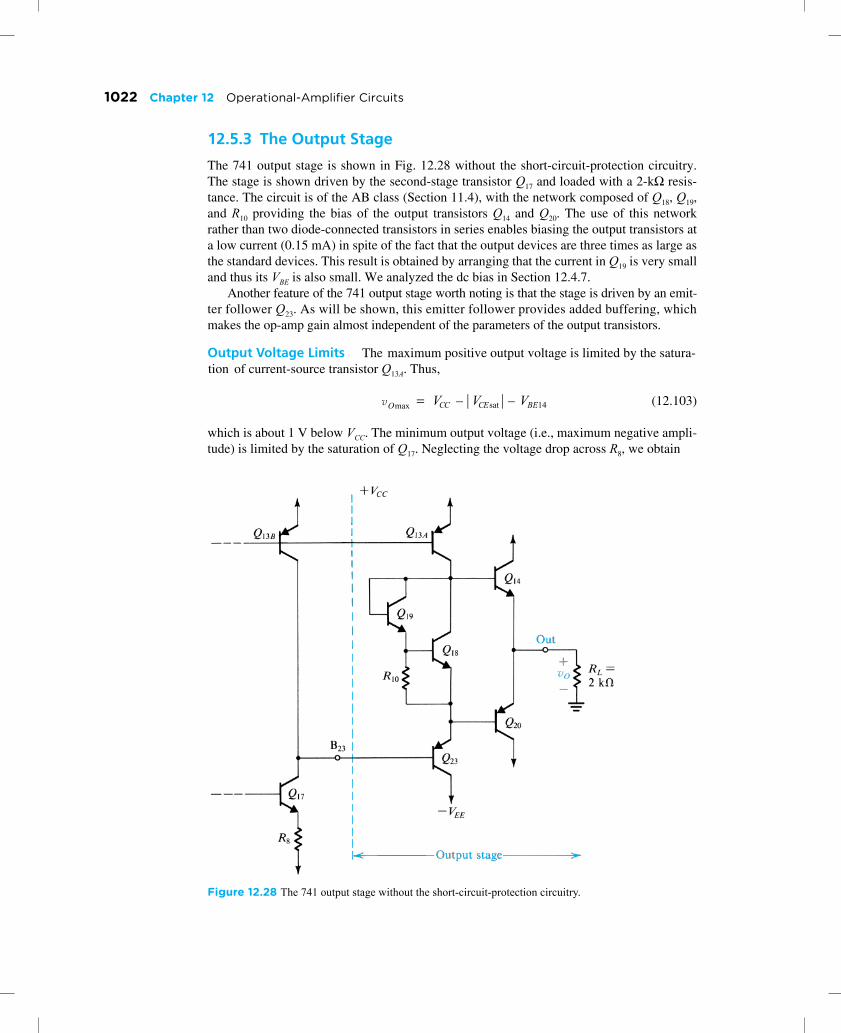
1022 Chapter 12 Operational-Amplifier Circuits
12.5.3 The Output Stage
The 741 output stage is shown in Fig. 12.28 without the short-circuit-protection circuitry.The stage is shown driven by the second-stage transistor Q17 and loaded with a 2-kΩ resis-tance. The circuit is of the AB class (Section 11.4), with the network composed of Q18, Q19,and R10 providing the bias of the output transistors Q14 and Q20. The use of this networkrather than two diode-connected transistors in series enables biasing the output transistors ata low current (0.15 mA) in spite of the fact that the output devices are three times as large asthe standard devices. This result is obtained by arranging that the current in Q19 is very smalland thus its VBE is also small. We analyzed the dc bias in Section 12.4.7.
Another feature of the 741 output stage worth noting is that the stage is driven by an emit-ter follower Q23. As will be shown, this emitter follower provides added buffering, whichmakes the op-amp gain almost independent of the parameters of the output transistors.
Output Voltage Limits The maximum positive output voltage is limited by the satura-tion of current-source transistor Q13A. Thus,
(12.103)
which is about 1 V below VCC. The minimum output voltage (i.e., maximum negative ampli-tude) is limited by the saturation of Q17. Neglecting the voltage drop across R8, we obtain
Figure 12.28 The 741 output stage without the short-circuit-protection circuitry.
vOmax VCC VCEsat VBE14––=

12.5 Small-Signal Analysis of the 741 1023
(12.104)
which is about 1.5 V above −VEE.
Small-Signal Model We shall now carry out a small-signal analysis of the output stagefor the purpose of determining the values of the parameters of the equivalent-circuit modelshown in Fig. 12.29. The model is shown fed by vo2, which is the open-circuit output voltageof the second stage. From Fig. 12.27, vo2 is given by
(12.105)
where Gm2 and Ro2 were previously determined as Gm2 = 6.5 mA/V and Ro2 = 81 kΩ. Resis-tance Rin3 is the input resistance of the output stage determined with the amplifier loadedwith RL. Although the effect of loading an amplifier stage on its input resistance is negligiblein the input and second stages, this is not the case in general in an output stage. Defining Rin3
in this manner enables correct evaluation of the voltage gain of the second stage, A2, as
(12.106)
To determine Rin3, assume that one of the two output transistors—say, Q20—is conductinga current of, say, 5 mA while Q14 is cutoff. It follows that the input resistance looking intothe base of Q20 is approximately β20RL. Assuming β20 = 50, for RL = 2 kΩ, the input resis-tance of Q20 is 100 kΩ. This resistance appears in parallel with the series combination of theoutput resistance of Q13A (ro13A � 280 kΩ) and the resistance of the Q18–Q19 network. The latterresistance is very small (about 160 Ω; see later: Exercise 12.23). Thus the total resistance inthe emitter of Q23 is approximately (100 kΩ || 280 kΩ) or 74 kΩ and the input resistance Rin3
is given by
which for β23 = 50 is Rin3 � 3.7 MΩ. Since Ro2 = 81 kΩ, we see that Rin3 � Ro2, and thevalue of Rin3 will have little effect on the performance of the op amp. Still we can use the valueobtained for Rin3 to determine the gain of the second stage using Eq. (12.106) as A2 = −515 V/V.The value of A2 will be needed in Section 12.6 in connection with the frequency-responseanalysis.
Continuing with the determination of the equivalent circuit-model-parameters, we notefrom Fig. 12.29 that Gv o3 is the open-circuit overall voltage gain of the output stage,
(12.107)
Figure 12.29 Model for the 741 output stage.
Rout
Rin3 Gvo3vo2
vOmin V– EE VCEsat VEB23 VEB20+ + +=
vo2 Gm2Ro2vi2–=
A2vi3
vi2------≡ Gm2Ro2–
Rin3
Rin3 Ro2+----------------------=
Rin3 � β23 74 kΩ×
Gvo3vo
vo2-------
RL ∞=
=

1024 Chapter 12 Operational-Amplifier Circuits
With RL = ∞, the gain of the emitter-follower output transistor (Q14 or Q20) will be nearlyunity. Also, with RL = ∞ the resistance in the emitter of Q23 will be very large. This meansthat the gain of Q23 will be nearly unity and the input resistance of Q23 will be very large.We thus conclude that Gvo3 � 1.
Next, we shall find the value of the output resistance of the op amp, Rout. For this purposerefer to the circuit shown in Fig. 12.30. In accordance with the definition of Rout fromFig. 12.29, the input source feeding the output stage is grounded, but its resistance (which isthe output resistance of the second stage, Ro2) is included. We have assumed that the outputvoltage vO is negative, and thus Q20 is conducting most of the current; transistor Q14 has there-fore been eliminated. The exact value of the output resistance will of course depend on whichtransistor (Q14 or Q20) is conducting and on the value of load current. Nevertheless, we wish tofind an estimate of Rout.
As indicated in Fig. 12.30, the resistance seen looking into the emitter of Q23 is
(12.108)
Substituting Ro2 = 81 kΩ, β23 = 50, and re23 = 25/0.18 = 139 Ω yields Ro23 = 1.73 kΩ. Thisresistance appears in parallel with the series combination of ro13A and the resistance of theQ18–Q19 network. Since ro13A alone (0.28 MΩ) is much larger than Ro23, the effective resis-tance between the base of Q20 and ground is approximately equal to Ro23. Now we can findthe output resistance Rout as
(12.109)
For β20 = 50, the first component of Rout is 34 Ω. The second component depends criticallyon the value of output current. For an output current of 5 mA, re20 is 5 Ω and Rout is 39 Ω. Tothis value we must add the resistance R7 (27 Ω) (see Fig. 12.13), which is included for short-circuit protection. The output resistance of the 741 is specified to be typically 75 Ω.
Figure 12.30 Circuit for finding the output resistance Rout.
Rout �
Ro23Ro2
β23 1+---------------- re23+=
RoutRo23
β20 1+---------------- re20+=

12.5 Small-Signal Analysis of the 741 1025
12.23 Using a simple (rπ, gm) model for each of the two transistors Q18 and Q19 in Fig. E12.23, find thesmall-signal resistance between A and A′. (Note: From Table 12.1, IC18 = 165 μA and IC19 �16 μA. Ans. 163 Ω
12.24 Figure E12.24 shows the circuit for determining the op-amp output resistance when vO is positiveand Q14 is conducting most of the current. Using the resistance of the Q18–Q19 network calculatedin Exercise 12.23 and neglecting the large output resistance of Q13A, find Rout when Q14 is sourcingan output current of 5 mA.Ans. 14.4 Ω
Figure E12.23
Rout
Figure E12.24
EXERCISES

1026 Chapter 12 Operational-Amplifier Circuits
Output Short-Circuit Protection If the op-amp output terminal is short-circuited toone of the power supplies, one of the two output transistors could conduct a large amount ofcurrent. Such a large current can result in sufficient heating to cause burnout of the IC(Chapter 11). To guard against this possibility, the 741 op amp is equipped with a specialcircuit for short-circuit protection. The function of this circuit is to limit the current in theoutput transistors in the event of a short circuit.
Refer to Fig. 12.13. Resistance R6 together with transistor Q15 limits the current thatwould flow out of Q14 in the event of a short circuit. Specifically, if the current in the emit-ter of Q14 exceeds about 20 mA, the voltage drop across R6 exceeds 540 mV, which turnsQ15 on. As Q15 turns on, its collector robs some of the current supplied by Q13A, thus reduc-ing the base current of Q14. This mechanism thus limits the maximum current that the opamp can source (i.e., supply from the output terminal in the outward direction) to about20 mA.
Limiting of the maximum current that the op amp can sink, and hence the currentthrough Q20, is done by a mechanism similar to the one discussed above. The relevant circuitis composed of R7, Q21, Q24, and Q22. For the components shown, the current in the inwarddirection is limited also to about 20 mA.
12.6 Gain, Frequency Response, andSlew Rate of the 741
In this section we shall evaluate the overall small-signal voltage gain of the 741 op amp. Weshall then consider the op amp’s frequency response and its slew-rate limitation.
12.6.1 Small-Signal Gain
The overall small-signal gain can be found from the cascade of the equivalent circuitsderived in the preceding sections for the three op-amp stages. This cascade is shown inFig. 12.31, loaded with RL = 2 kΩ, which is the typical value used in measuring and specify-ing the 741 data. The overall gain can be expressed as
(12.110)
(12.111)
Figure 12.31 Cascading the small-signal equivalent circuits of the individual stages for the evaluation ofthe overall voltage gain.
vovi----
vi2vi-----
vo2vi2------
vovo2------=
Gm1 Ro1 || Ri2( ) Gm2Ro2–( )Gvo3RL
RL Rout+--------------------–=
Rin3
Rout
Gvo3vo2

12.6 Gain, Frequency Response, and Slew Rate of the 741 1027
Using the values found earlier yields for the overall open-circuit voltage gain,
(12.112)
12.6.2 Frequency Response
The 741 is an internally compensated op amp. It employs the Miller compensation tech-nique, studied in Section 10.13.3, to introduce a dominant low-frequency pole. Specifically,a 30-pF capacitor (CC) is connected in the negative-feedback path of the second stage. Anapproximate estimate of the frequency of the dominant pole can be obtained as follows.
From Miller’s theorem (Section 9.4.4), we see that the effective capacitance due to CCbetween the base of Q16 and ground is (see Fig. 12.13)
(12.113)
where A2 is the second-stage gain. Use of the value calculated for A2 in Section 12.5.3, A2 =−515, results in Cin = 15,480 pF. Since this capacitance is quite large, we shall neglect allother capacitances between the base of Q16 and signal ground. The total resistance betweenthis node and ground is
(12.114)
Thus the dominant pole has a frequency fP given by
(12.115)
It should be noted that this approach is equivalent to using the approximate formula inEq. (10.116).
As discussed in Section 10.13.3, Miller compensation provides an additional advanta-geous effect, namely, pole splitting. As a result, the other poles of the circuit are moved tovery high frequencies. This has been confirmed by computer-aided analysis [see Gray et al(2000)].
Assuming that all nondominant poles are at very high frequencies, the calculated valuesgive rise to the Bode plot shown in Fig. 12.32, where f3dB = fP. The unity-gain bandwidth f t canbe calculated from
(12.116)
Thus,
(12.117)
Although this Bode plot implies that the phase shift at f t is −90° and thus that the phasemargin is 90°, in practice a phase margin of about 80° is obtained. The excess phase shift(about 10°) is due to the nondominant poles. This phase margin is sufficient to provide stableoperation of closed-loop amplifiers with any value of feedback factor β. This convenience of
A0vovi----≡ 476.1– 526.5–( ) 0.97×× 243,147 V/V= =
≡ 107.7 dB
Cin CC 1 A2+( )=
Rt Ro1 || Ri2=
6.7 MΩ || 4 MΩ= 2.5 MΩ=
fP1
2πCinRt------------------- 4.1 Hz= =
ft A0f3dB=
ft 243,147 4.1× � 1 MHz=

1028 Chapter 12 Operational-Amplifier Circuits
use of the internally compensated 741 is achieved at the expense of a great reduction inopen-loop gain and hence in the amount of negative feedback. In other words, if one requiresa closed-loop amplifier with a gain of 1000, then the 741 is overcompensated for such anapplication, and one would be much better off designing one’s own compensation (assuming,of course, the availability of an op amp that is not already internally compensated).
12.6.3 A Simplified Model
Figure 12.33 shows a simplified model of the 741 op amp in which the high-gain secondstage, with its feedback capacitance CC, is modeled by an ideal integrator. In this model, thegain of the second stage is assumed to be sufficiently large that a virtual ground appears atits input. For this reason the output resistance of the input stage and the input resistance ofthe second stage have been omitted. Furthermore, the output stage is assumed to be an idealunity-gain follower. Except for the presence of the output stage, this model is identical tothat which we used for the two-stage CMOS amplifier in Section 12.1.4 (Fig. 12.3).
Analysis of the model in Fig. 12.33 gives
(12.118)
Figure 12.32 Bode plot for the 741 gain, neglecting nondominant poles.
Figure 12.33 A simple model for the 741 based on modeling the second stage as an integrator.
�
A s( )Vo s( )Vi s( )-------------≡
Gm1
sCC---------=

12.6 Gain, Frequency Response, and Slew Rate of the 741 1029
Thus,
(12.119)
and the magnitude of gain becomes unity at ω = ωt, where
(12.120)
Substituting Gm1 = 1/5.26 mA/V and CC = 30 pF yields
(12.121)
which is equal to the value calculated before. It should be pointed out, however, that thismodel is valid only at frequencies f � f3dB. At such frequencies the gain falls off with aslope of −20 dB/decade, just like that of an integrator.
12.6.4 Slew Rate
The slew-rate limitation of op amps is discussed in Chapter 2. Here we shall illustrate theorigin of the slewing phenomenon in the context of the 741 circuit. This development is sim-ilar to that we presented for the CMOS op-amp in Section 12.1.6.
Consider the unity-gain follower of Fig. 12.34 with a step of, say, 10 V applied at theinput. Because of amplifier dynamics, its output will not change in zero time. Thus immedi-ately after the input is applied, almost the entire value of the step will appear as a differentialsignal between the two input terminals. This large input voltage causes the input stage to beoverdriven, and its small-signal model no longer applies. Rather, half the stage cuts off andthe other half conducts all the current. Specifically, reference to Fig. 12.13 shows that alarge positive differential input voltage causes Q1 and Q3 to conduct all the available biascurrent (2I) while Q2 and Q4 will be cut off. The current mirror Q5, Q6, and Q7 will still func-tion, and Q6 will produce a collector current of 2I.
Using the observations above, and modeling the second stage as an ideal integrator,results in the model of Fig. 12.35. From this circuit we see that the output voltage will be aramp with a slope of 2I/CC:
(12.122)
Figure 12.34 A unity-gain follower with a large step input. Since the output voltage cannot change instan-taneously, a large differential voltage appears between the op-amp input terminals.
A jω( )Gm1
jωCC-------------=
ωtGm1
CC---------=
ftωt
2π------ � 1 MHz=
vO t( ) 2ICC------t=

1030 Chapter 12 Operational-Amplifier Circuits
Thus the slew rate SR is given by
(12.123)
For the 741, I = 9.5 μA and CC = 30 pF, resulting in SR = 0.63 V/μs.It should be pointed out that this is a rather simplified model of the slewing process.
More detail can be found in Gray et al., (2000).
12.6.5 Relationship Between ft and SR
A simple relationship exists between the unity-gain bandwidth f t and the slew rate SR. Thisrelationship is obtained by combining Eqs. (12.120), (12.123), and
(12.124)
and then using Eq. (12.83′) to obtain
(12.125)
Now, since gm1 is the transconductance of each of Q1 through Q4,
(12.126)
Thus,
(12.127)
As a check, for the 741 we have
Figure 12.35 Model for the 741 op amp when a large positive differential signal is applied.
SR 2ICC------=
12.25 Use the value of the slew rate calculated above to find the full-power bandwidth fM of the 741 opamp. Assume that the maximum output is ±10 V.Ans. 10 kHz
EXERCISE
SR 2IGm1---------ωt=
SR 4Igm1--------ωt=
gm1I
VT-----=
SR 4VTωt=
SR 4 25 10 3– 2π 106×××× 0.63 V/μs= =

12.7 Modern Techniques for the Design of BJT Op Amps 1031
which is the result obtained previously. Observe that Eq. (12.127) is of the same form asEq. (12.42), which applies to the two-stage CMOS op amp. Here, 4VT replaces VOV. Since, typi-cally, VOV will be two to three times the value of 4VT , a two-stage CMOS op amp with an ftequal to that of the 741 exhibits a slew rate that is two to three times as large as that of the 741.
A general form for the relationship between SR and ωt for an op amp with a structuresimilar to that of the 741 (including the two-stage CMOS circuit) is
(12.128)
where a is the constant of proportionality relating the transconductance of the first stageGm1, to the total bias current of the input differential stage. That is, for the 741 circuitGm1 = a(2I ), while for the CMOS circuit of Fig. 12.1, Gm1 = aI.3 For a given ωt, a highervalue of SR is obtained by making a smaller; that is, the total bias current is kept con-stant and Gm1 is reduced. This is a viable technique for increasing slew rate. It is referred to asthe Gm-reduction method (see Exercise 12.27).
12.7 Modern Techniques for the Design of BJT Op Amps
Although the ingenious techniques employed in the design of the 741 op amp have stood thetest of time, they are now more than 40 years old! Technological advances have resulted inchanges in the user requirements of general-purpose bipolar op amps. The resulting moredemanding specifications have in turn posed new challenges to analog IC designers who, asthey have done repeatedly before, are responding with new and exciting circuits. In this sectionwe present a sample of recently developed design techniques. For more on this rather advancedtopic the reader is referred to the Analog Circuits section of the bibliography in Appendix G.
12.7.1 Special Performance Requirements
Many of the special performance requirements stem from the need to operate modern op ampsfrom power supplies of much lower voltages. Thus while the 741-type op amp operated from
3The difference is just a matter of notation; We used I to denote the total bias current of the input differential stage of the CMOS circuit, and we used 2I for the 741 case!
SR ωt a⁄=
12.26 Consider the integrator model of the op amp in Fig. 12.33. Find the value of the resistor that, whenconnected across CC, provides the correct value of the dc gain.Ans. 1279 MΩ
D12.27 If a resistance RE is included in each of the emitter leads of Q3 and Q4 show that SR = 4(VT + IRE / 2)ωt.Hence find the value of RE that would double the 741 slew rate while keeping ωt and I unchanged.What are the new values of CC, the dc gain, and the 3-dB frequency?Ans. 5.26 kΩ; 15 pF; 101.7 dB (a 6-dB decrease); 8.2 Hz
EXERCISES

1032 Chapter 12 Operational-Amplifier Circuits
power supplies, many modern BJT op amps are required to operate from a single powersupply of only 2 V to 3 V. This is done for a number of reasons, including the following.
1. Modern small-feature-size IC fabrication technologies require low power-supplyvoltages.
2. Compatibility must be achieved with other parts of the system that use low-voltagesupplies.
3. Power dissipation must be minimized, especially for battery-operated equipment.
As Fig. 12.36 indicates, there are two important changes: the use of a single ground-refer-enced power supply , and the low value of . Both of these requirements give rise tochanges in performance specifications and pose new design challenges. In the following wediscuss two of the resulting changes.Rail-to-Rail Input Common-Mode Range Recall that the input common-mode rangeof an op amp is the range of common-mode input voltages for which the op amp operatesproperly and meets its performance specifications, such as voltage gain and CMRR. Op ampsof the 741 type operate from supplies and exhibit an input common-mode range thatextends to within a couple of volts of each supply. Such a gap between the input common-mode range and the power supply is obviously unacceptable if the op amp is to be operatedfrom a single supply that is only 2 V to 3 V. Indeed we will now show that these single-sup-ply, low-voltage op amps need to have an input common-mode range that extends over theentire supply voltage, 0 to , referred to as rail-to-rail input common mode range.
Consider first the inverting op-amp configuration shown in Fig. 12.37(a). Since the posi-tive input terminal is connected to ground (which is the voltage of the negative-supply rail),
Figure 12.36 Power supply requirements have changed considerably. Modern BJT op amps are requiredto operate from a single supply VCC of 2 to 3 V.
Figure 12.37 (a) In the inverting configuration, the + ive op-amp input is connected to ground; thus it isimperative that the input common-mode range includes ground. (b) In the unity-gain follower configuration,vICM = vI ; thus it is highly desirable for the input common-mode range to include ground and VCC .
�
�Modern
VCC � 3 V
�
�741
VCC � �15 V
�VEE � �15 V
15-V±
VCC VCC
15-V±
VCC
�
�
VCC
vO
vI�
�
VCC
R2
R1
vO
vI
(a) (b)

12.7 Modern Techniques for the Design of BJT Op Amps 1033
ground voltage has to be within the allowable input common-mode range. In fact, becausefor positive output voltages the voltage at the inverting input terminal can go slightly nega-tive, the input common-mode range should extend below the negative-supply rail (ground).
Next consider the unity-gain voltage follower obtained by applying 100% negative feed-back to an op amp, as shown in Fig. 12.37(b). Here the input common-mode voltage is equalto the input signal . To maximize the usefulness of this buffer amplifier, its input signal should be allowed to extend from 0 to , especially since is only 2 to 3 V. Thus theinput common-mode range should include also the positive supply rail. As will be seenshortly, modern BJT op amps can operate over an input common-mode voltage range thatextends a fraction of a volt beyond its two supply rails: that is, more than rail-to-railoperation!Near Rail-to-Rail Output Signal Swing In the 741 op amp, we were satisfied with anoutput that can swing to within 2 V or so of each of the supply rails. With a supply of ,this capacity resulted in a respectable output range. However, to limit the output swingto within 2 V of the supply rails in an op amp operating from a single 3-V supply would resultin an unusable device! Thus, here too, we require near rail-to-rail operation. As we shall seein Section 12.7.5, this requirement forces us to adopt a whole new approach to output-stagedesign.Device Parameters The technology we shall use in the examples, exercises, and prob-lems for this section has the following characteristics:
VA = 30 V= 20 V
For both, and . It is important to note that we will assume thatfor this technology, the transistor will remain in the active mode for as low as 0.1 V (inother words, that 0.6 V is needed to forward-bias the CBJ).
12.7.2 Bias Design
As in the 741 circuit, the bias design of modern BJT amplifiers makes extensive use of cur-rent mirrors and current-steering circuits (Sections 7.4 and 7.5). Typically, however, the biascurrents are small (in the micro amp range). Thus, the Widlar current source (Section 7.5.5)is especially popular here. As well, emitter-degeneration resistors (in the tens-of-kilohmrange) are frequently used.
Figure 12.38 shows a self-biased current-reference source that utilizes a Widlar cir-cuit formed by , , and , and a current mirror with matched emitter-degeneration resistors and . The circuit establishes a current I in each of the fourtransistors, with the value of I determined as follows. Neglecting base currents and ’sfor simplicity, we write
Thus,
vI vIVCC VCC
15 V±13-V±
npn Transistors: β 40=
pnp Transistors: β 10= VA
VBE � 0.7 V VCEsat � 0.1 VVCE
Q1 Q2 R2 Q3 Q4–R3 R4
ro
VBE1 VT ln IIS1------⎝ ⎠⎛ ⎞=
VBE2 VT ln IIS2------⎝ ⎠⎛ ⎞=
VBE1 VBE2 V= T ln IS2
IS1------⎝ ⎠⎛ ⎞–

1034 Chapter 12 Operational-Amplifier Circuits
But,
Thus,
(12.129)
Thus the value of I is determined by and the ratio of the emitter areas of and Also, observe that I is independent of a highly desirable outcome. Neglecting the tem-perature dependence of we see that I is directly PTAT (proportional to the absolute tem-perature T ). It follows that transistors biased by I or mirrored versions of it will exhibit ’sthat are constant independent of temperature!
The circuit in Fig. 12.38 provides a bias line with a voltage equal to . This canbe used to bias other transistors and thus generate currents proportional to I by appropriatelyscaling their emitter areas. Similarly, the circuit provides a bias line at a voltage
below . This bias line can be used to bias other transistors and thus generateconstant currents proportional to I by appropriately scaling emitter areas and emitter-degeneration resistances. These ideas are illustrated in Fig. 12.39.
R4
CC
R3
Q3Q4VBIAS 2
Q2Q1VBIAS 1
R2
II
Figure 12.38 A self-biased current-reference source utilizing a Widler circuit to generate I = VT /R2ln(IS2/IS1)The bias voltages VBIAS1 and VBIAS2 are utilized in other parts of the op-amp circuit for biasing other transistors.
VBE1 VBE2 IR2=–
IVT
R2------ ln
IS2
IS1------⎝ ⎠⎛ ⎞=
R2 Q1 Q2.VCC,
R2,gm
D12.28 Design the circuit in Fig. 12.38 to generate a current I = 10 μA. Utilize transistors and having their areas in a 1:2 ratio. Assume that and are matched and design for a 0.2-V dropacross each of and Specify the values of and Ans. 1.73 ; 20 ; 20
Q1 Q2Q3 Q4
R3 R4. R2, R3, R4.kΩ kΩ kΩ
EXERCISE
VBIAS1 VBE1
VBIAS2IR3 VEB3+( ) VCC
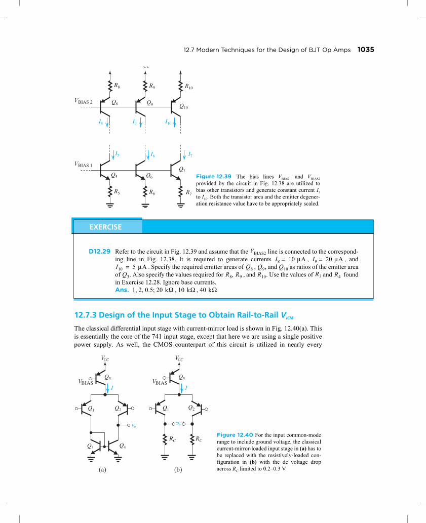
12.7 Modern Techniques for the Design of BJT Op Amps 1035
12.7.3 Design of the Input Stage to Obtain Rail-to-Rail VICM
The classical differential input stage with current-mirror load is shown in Fig. 12.40(a). Thisis essentially the core of the 741 input stage, except that here we are using a single positivepower supply. As well, the CMOS counterpart of this circuit is utilized in nearly every
VBIAS 2
VCC
Q8 Q9 Q10
R8
I8 I9 I10
R9 R10
VBIAS 1
Q5 Q6
Q7
R5
I5 I6 I7
R6 R7
Figure 12.39 The bias lines VBIAS1 and VBIAS2provided by the circuit in Fig. 12.38 are utilized tobias other transistors and generate constant current I5to I10. Both the transistor area and the emitter degener-ation resistance value have to be appropriately scaled.
D12.29 Refer to the circuit in Fig. 12.39 and assume that the line is connected to the correspond-ing line in Fig. 12.38. It is required to generate currents , , and
. Specify the required emitter areas of , , and as ratios of the emitter areaof . Also specify the values required for , , and . Use the values of and foundin Exercise 12.28. Ignore base currents.Ans. 1, 2, 0.5; 20 , 10 , 40
VBIAS2I8 10 μA= I9 20 μA=
I10 5 μA= Q8 Q9 Q10Q3 R8 R9 R10 R3 R4
kΩ kΩ kΩ
EXERCISE
vo
Q1 Q2
Q5
Q3 Q4
IVBIAS
VCC
vo
Q1 Q2
Q5
IVBIAS
(a) (b)
VCC
RC RCFigure 12.40 For the input common-moderange to include ground voltage, the classicalcurrent-mirror-loaded input stage in (a) has tobe replaced with the resistively-loaded con-figuration in (b) with the dc voltage dropacross RC limited to 0.2–0.3 V.

1036 Chapter 12 Operational-Amplifier Circuits
CMOS op-amp design (see Section 12.1). Unfortunately, this very popular circuit does notmeet our requirement of rail-to-rail common-mode operation.
Consider first the low end of the input common-mode range. The value of is lim-ited by the need to keep in the active mode. Specifically, since the collector of is at avoltage V, we see that the voltage applied to the base of cannot go lowerthan 0.1 V without causing the collector–base junction of to become forward biased.Thus V, and the input common-mode range does not include ground voltageas required.
The only way to extend to 0 V is to lower the voltage at the collector of . Thisin turn can be achieved only by abandoning the use of the current-mirror load and utilizinginstead resistive loads, as shown in Fig. 12.40(b). Observe that in effect we are going back tothe resistively loaded differential pair with which we began our study of differential amplifi-ers in Chapter 8!
The minimum allowed value of in the circuit of Fig. 12.40(b) is still of course lim-ited by the need to keep and in the active mode. This in turn is achieved by avoiding
values that cause the base voltages of and to go below their collector voltagesby more than 0.6 V,
where is the voltage drop across each of and . Now if is selected to be 0.2 to0.3 V, then will be V to , which is exactly what we need.
The major drawback of replacing the current-mirror load with resistive loads is that thedifferential gain realized is considerably reduced,
where we have neglected for simplicity. Thus for , the gain realized is only12 V/V. As we will see shortly, this low-gain problem can be solved by cascoding.
Next consider the upper end of the input common-mode range. Reference to the circuitin Fig. 12.40(b) shows that the maximum voltage that can be applied to the bases of and is limited by the need to keep the current-source transistor in the active mode. Thisin turn is achieved by ensuring that the voltage across , does not fall below 0.1 Vor so. Thus the maximum value of will be a voltage or approximately 0.7 Vlower,
That is, the upper end of the input common-mode range is at least 0.8 V below , a severelimitation.
To recap, while the circuit in Fig. 12.40(b) has of a few tenths of a volt below thenegative power-supply rail (at ground voltage), the upper end of is rather far from
,
VICMminQ1 Q1
VBE3 � 0.7 Q1Q1
VICMmin 0.1=
VICMmin Q1
VICMQ1 Q2
VICM Q1 Q2
VICMmin VRC0.6 V–=
VRCRC1 RC2 VRC
VICMmin 0.4– 0.3 V–
vovid------ gm1 2, RC–=
I 2⁄VT--------- RC
VRC
VT--------–=–=
ro VRC0.3 V=
Q1Q2
Q5 VEC5VICM VEB1 2,
VICMmax VCC 0.1– 0.7 VCC 0.8–=–=
VCC
VICMminVICM
VCC
0.3 VICM VCC 0.8–≤ ≤–

12.7 Modern Techniques for the Design of BJT Op Amps 1037
where we have assumed . To extend the upper end of , we adopt a solutionsimilar to that used in the CMOS case (Section 12.2.6, Fig. 12.11), namely, we utilize a par-allel complementary input stage. Toward that end, note that the npn version of the circuit ofFig. 12.40(b), shown in Fig. 12.41, has a common-input range of
where we have assumed that . Thus, as expected, the high end meets our specifi-cations and in fact is above the positive supply rail by 0.3 V. The lower end, however, doesnot; but this should cause us no concern because the lower end will be looked after by thepnp pair. Finally, note that there is a range of in which both the pnp and the npn cir-cuits will be active and properly operating,
Figure 12.42 shows an input stage that achieves more than rail-to-rail input common-mode range by utilizing a pnp differential pair ( , ) and an npn differential pair ( , ),connected in parallel. To keep the diagram simple, we are not showing the parallel connec-tion of the input terminals; the + input terminals are assumed to be connected together, andsimilarly for the – input terminals. In order to increase the gain obtained from the resistivelyloaded differential pairs, a folded cascode stage is added. Here and are the resistiveloads of the pnp pair , and are its cascode transistors. Similarly, and are the resistive loads of the npn pair and are its cascode transistors.Observe that the cascode transistors do “double duty.” For instance, operate as thecascode devices for and at the same time as current-source loads for . Asimilar statement can be made about . The output voltage of the first stage, , istaken between the collectors of the cascode devices.
For , the npn stage will be inactive and the gain is determined by thetransconductance of the pair together with the output resistance seen betweenthe collectors of the cascode transistors. At the other end of , that is, ,the stage will be inactive, and the gain will be determined by the transconductance
of the pair and the output resistance between the collectors of the cascodedevices. In the overlap region both the pnp and npn stages will beactive and their effective transconductances add up, thus resulting in a higher gain. Thedependence of the differential gain on the input common-mode is usually undesirable
VRC0.3 V= VICM
RC RC
vo
VCC
VBIAS
Q3 Q4
Q6Figure 12.41 The complement of the circuit in Fig. 12.40(b). Whilethe input common-mode range of the circuit in Figure 12.40(b) extendsbelow ground, here it extends above VCC. Connecting the two circuits inparallel, as will be shown, results in a rail-to-rail VICM range.
0.8 VICM VCC 0.3+≤ ≤
VRC0.3 V=
VICM
0.8 VICM VCC 0.8–≤ ≤
Q1 Q2 Q3 Q4
R7 R8Q1 Q2– Q7 Q8– R9 R10
Q3 Q4,– Q9 Q10–Q7 Q8–
Q1 Q2– Q9 Q10–Q9 Q10– vod
VICM � 0.8 VGm Q1 Q2–
VICM VICM � VCC 0.8–Q1 Q2–
Gm Q3 Q4–0.8 VICM VCC 0.8,–≤ ≤
GmVICM

1038 Chapter 12 Operational-Amplifier Circuits
and can be reduced considerably by arranging that one of the two differential pairs is turnedoff when the other one is active.4
4This is done in the NE5234 op amp, whose circuit is described and analyzed in great detail in Gray et al., (2009).
R9
VCC
VB
R10
Q10
Q9 VBIAS 3
VBQ8Q7
vO2
vO1 vod
R8R7
Q1 Q2
Q5
VBIAS 1
npn pair pnp pair Cascode
Q3Q4
Q6VBIAS2
�
�
��
� �
Figure 12.42 Input stage with rail-to-rail input common-mode range and a folded-cascode stage toincrease the gain. Note that all the bias voltages including VBIAS3 and VB are generated elsewhere on thechip.
It is required to find the input resistance and the voltage gain of the input stage shown in Fig. 12.42. Let so that the pair is off. Assume that supplies 10 μA, that each of to is
biased at 10 μA, and that all four cascode transistors are operating in the active mode. The input resis-tance of the second stage of the op amp (not shown) is . The emitter-degeneration resistancesare , and Recall that the device parameters are
V, V.
Solution
Since the stage is fully balanced, we can use the differential half-circuit shown in Fig. 12.43(a). The inputresistance is twice the value of
where
VICM � 0.8 V Q3 Q4– Q5 Q7 Q10
RL 2 MΩ=R7 R8 20 kΩ== R9 R10 30 kΩ.== βN 40,=
βP 10,= VAn 30= VAp 20=
Rid rπ1,
Rid 2rπ1 2βP gm1⁄==
gm1IC1
VT------- 5 10 6–×
25 10 3–×---------------------- 0.2 mA/V===
Example 12.5

12.7 Modern Techniques for the Design of BJT Op Amps 1039
Thus,
To find the short-circuit transconductance, we short the output to ground as shown in Fig. 12.43(b) andfind as
At node X we have four parallel resistances to ground,
Obviously and are very large and can be neglected. Then, the portion of that flowsinto the emitter proper of can be found from
and the output short-circuit current is
RL
2
Q1
Q1
Q7
R9
(b)(a)
vid
2� � vodRo9
Ro7 2
Rid �2
� � � �
Q7
R7
R7
Q9
vid
re7X
ro7
ro1
ie7
io
2
gm1vid
2� �
Figure 12.43 (a) Differential half circuit for the input stage shown in Fig. 12.42 with VICM 0.8 V. (b) Determining�Gm1 io vid 2⁄( )⁄=
Rid2 10×
0.2--------------- 100 kΩ==
Gm1
Gm1ic7
vid 2⁄-------------=
ro1VAp
IC1----------- 20 V
5 μA------------- 4 MΩ===
R7 20 kΩ=
ro7VAn
IC7-------- 30 V
10 μA---------------- 3 MΩ===
re7 � 1gm7--------
VT
IC7------- 25 mV
10 μA---------------- 2.5 kΩ===
ro1 ro7 gm1 vid 2⁄( )Q7
ie7 � gm1vid
2------⎝ ⎠⎛ ⎞ R7
R7 re7+-------------------⎝ ⎠
⎛ ⎞
gm1vid
2------⎝ ⎠⎛ ⎞ 20
20 2.5+------------------- 0.89gm1
vid
2------⎝ ⎠⎛ ⎞==
io
io � ie7 0.89gm1 vid 2⁄( )=

1040 Chapter 12 Operational-Amplifier Circuits
Example 12.5 continued
Thus,
To find the voltage gain, we need to determine the total resistance between the output node and groundfor the circuit in Fig. 12.43(a),
The resistance is the output resistance of , which has an emitter-degeneration resistance Thus can be found using Eq. (7.50),
where
Thus
The resistance is the output resistance of which has an emitter-degeneration resistance Thus,
where
Thus,
Gm1io
vid 2⁄------------- 0.89gm1 0.89 0.2 0.18 mA/V=×==≡
R Ro9 Ro7 RL 2⁄( )|| ||=
Ro9 Q9 R9.Ro9
Ro9 ro9 R9 rπ 9||( ) 1 gm9+ ro9( )+=
ro9VAp
IC9----------- 20 V
10 μA---------------- 2 MΩ===
gm9IC9
VT------- 10 μA
25 mV---------------- 0.4 mA/V===
rπ 9βP
gm9-------- 10
0.4 mA/V------------------------ 25 kΩ===
Ro9 2 30 25||( ) 10 3–× 1 0.4 2 103××+( )+=
12.9 MΩ=
Ro7 Q7,R7 ro1||( ) � R7.
Ro7 ro7 R7 rπ7||( ) 1 gm7+ ro7( )+=
ro7VAn
IC7-------- 30 V
10 μA--------------- 3 MΩ===
gm7IC7
VT------- 10 μA
25 mV---------------- 0.4 mA/V===
rπ7βN
gm7-------- 40
0.4------- 100 kΩ===
Ro7 3 20 100||( ) 10 3–× 1 0.4 3 103××+( )+=
23 MΩ=
RL
2------ 2 MΩ
2--------------- 1 MΩ==

12.7 Modern Techniques for the Design of BJT Op Amps 1041
12.7.4 Common-Mode Feedback to Control the dc Voltage at the Output of the Input Stage
For the cascode circuit in Fig. 12.42 to operate properly and provide high output resistanceand thus high voltage gain, the cascode transistors Q7 through Q10 must operate in the activemode at all times. However, relying solely on matching will not be sufficient to ensure thatthe currents supplied by and are exactly equal to the currents supplied by and
Any small mismatch between the two sets of currents will be multiplied by the largeoutput resistance between each of the collector nodes and ground, and thus there will belarge changes in the voltages and These changes in turn can cause one set of thecurrent sources (i.e., or ) to saturate. We therefore need a circuit that detectsthe change in the dc or common-mode component of and
(12.130)
and adjusts the bias voltage on the bases of and to restore current equality. Thisnegative-feedback loop should be insensitive to the differential signal components of and otherwise it would reduce the differential gain. Thus the feedback loop should pro-vide common-mode feedback (CMF).
Figure 12.44 shows the cascode circuit with the CMF circuit shown as a black box. TheCMF circuit accepts and as inputs and provides the bias voltage as output. In aparticular implementation we will present shortly, the CMF circuit has the transfercharacteristic
(12.131)
By keeping higher than by only 0.4 V, the CMF circuit ensures that and remain active (0.6 V is needed for saturation).
The nominal value of is determined by the quiescent current of Q7 through Q10, thequiescent value of and and the value of and The resulting nominal value of
and the corresponding value of from Eq. (12.131) are designed to ensure that and operate in the active mode. Here, it is important to recall that is determinedby the rest of the op-amp bias circuit.
To see how the CMF circuit regulates the dc voltage , assume that for some reason is higher than it should be and as a result the currents of and exceed the currents
supplied by and by an increment When multiplied by the total resistancebetween each of the output nodes and ground, the increment will result in a large
The total resistance R can now be found as
Finally, we can find the voltage gain as
R 12.9 23 1 0.89 MΩ=|| ||=
Advod 2⁄vid 2⁄-------------- Gm1R1==
0.18 0.89 103×× 160 V/V==
Q9 Q10 Q7Q8. IΔ
vO1 vO2.Q7 Q8– Q9 Q10–
VCM vO1 vO2,
VCM12--- vO1 vO2+( )=
Q7 Q8, VB,vO1
vO2;
vO1 vO2 VB
VB VCM 0.4+=
VB VCM Q7 Q8
VBI1 I2, R7 R8.
VB VCM Q9Q10 VBIAS3
VCMVB Q7 Q8
Q9 Q10 I.ΔIΔ

1042 Chapter 12 Operational-Amplifier Circuits
negative voltage increment in and The CMF circuit responds by lowering to thevalue that restores the equality of currents. The change in needed to restore equilibriumis usually small (see Example 12.6 below) and according to Eq. (12.131) the correspondingchange in will be equally small. Thus we see negative feedback in action: It minimizesthe initial change and thus keeps nearly constant at its nominal value, which isdesigned to operate Q7 through Q10 in the active region.
We conclude by considering briefly a possible implementation of the CMF circuit. Figure12.45 shows the second stage of an op-amp circuit. The circuit is fed by the outputs of theinput stage, and
VCC
R10
Q9(determined bythe op amp
bias network)
Q8Q7
R8
R9
Q10
vO1
I3 I4
vO2 Common-ModeFeedback
Circuit
InOut
I1I2
R7
VB
VBIAS3
Figure 12.44 The cascode output circuit of the input stage and the CMF circuit that responds to the com-mon-mode component by adjusting VB so that Q7–Q8 conduct equal currents to Q9–Q10,and Q7–Q10 operate in the active mode.
VCM12--- vO1 vO2+( )=
vO1 vO2. VBVB
VCMVCM
vO2vO1
VBIAS
vo3
ID
VB
VE
Q13 Q14
Q11
D
Q12
Q15
Figure 12.45 An op amp second stage incorporating the common-mode feedback circuit for the inputstage. Note that the circuit generates the voltage VB needed to bias the cascode circuit in the first stage.Diode D is a Schottky-barrier diode which exhibits a forward voltage drop of about 0.4V.
vO1 vO2,

12.7 Modern Techniques for the Design of BJT Op Amps 1043
In addition to amplifying the differential component of the circuit generates a dc volt-age ,
To see how the circuit works, note that and are emitter followers that minimizethe loading of the second stage on the input stage. The emitter followers deliver to the basesof the differential pair voltages that are almost equal to and but dc shiftedby . Thus the voltage at the emitters of will be
which reduces to
The voltage is simply equal to plus the voltage drop of diode The latter is aSchottky barrier diode (SBD), which features a low forward drop of about 0.4 V. Thus,
as required.
vO1 VCM vd 2⁄+=
vO2 VCM vd 2⁄–=
vd,VB
VB VCM 0.4+=
Q11 Q12
Q13 Q14– vO1 vO2VEB11,12 Q13 Q14–
VE VCM VEB11,12 VBE13,14–+=
VE � VCM
VB VE D1.
VB VE VD VCM 0.4+=+=
Consider the operation of the circuit in Fig. 12.44. Assume that and thus the npn inputpair (Fig. 12.42) is off. Hence Also assume that only dc voltages are present and thus
Each of to is biased at 10 μA, , and Neglect base currents and neglect the loading effect of the
CMF circuit on the output nodes of the cascode circuit. The CMF circuit provides .
(a) Determine the nominal values of and . Does the value of ensure operation in the activemode for Q7 through Q10?
(b) If the CMF circuit were not present, what would be the change in and (i.e., in ) as aresult of a current mismatch between and ? Use the output resistancevalues found in Example 12.5.
(c) Now, if the CMF circuit is connected, what change will it cause in to eliminate the current mis-match ? What is the corresponding change in from its nominal value?
Solution
(a) The nominal value of is found as follows:
VICM � 0.8 VI3 I4 0.==
I1 I2 5 μA.== Q7 Q10 VCC 3 V,= VBIAS3 VCC 1–=R7 R8 20 kΩ,== R9 R10 30 kΩ.==
VB VCM 0.4+=
VB VCM VCM
vO1 vO2 VCMI 0.3 μA=Δ Q7 Q8– Q9 Q10–
VBIΔ VCM
VB
VB VBE7 IE7 I1+( )R7+=
� 0.7 10 5+( ) 10 3–× 20×+
1 V=
Example 12.6

1044 Chapter 12 Operational-Amplifier Circuits
Example 12.6 continued
The nominal value of can now be found from
For to be active,
that is,
For to be active
That is,
resulting in
Thus, for all four cascode transistors to operate in the active mode,
Thus the nominal value of 0.6 V ensures active mode operation.
(b) For
where is the output resistance between the collectors of and and ground,
In Example 12.5 we found that and ; thus,
Thus,
Now if is positive,
which exceeds the 2.6 V maximum allowed value before saturate. If is negative,
which is far below the V needed to keep in the active mode. Thus, in the absence of CMF,a current mismatch of would cause one set of the cascode transistors (depending on the polarityof ) to saturate.
VCM
VCM VB 0.4 1 0.4 0.6 V=–=–=
Q7 Q8–
VCM VB7 8, 0.6–>
VCM 0.4 V>
Q9 Q10–
VCM VBIAS3 0.6+<
VCM VCC 1– 0.6+<
VCM 2.6 V<
0.4 V VCM 2.6 V< <
IC9 IC7 IC10 IC8 I,Δ=–=–VCM IRo1Δ=Δ
Ro1 Q7 Q9
Ro1 Ro7 Ro9||=
Ro7 23 MΩ= Ro9 12.9=
Ro1 23 12.9 8.3 MΩ=||=
VCM 0.3 8.3 � 2.5 V×=Δ
VCMΔ
VCM 0.6 2.5 3.1 V=+=
Q9 Q10– VCMΔ
VCM 0.6 2.5 1.9 V–=–=
+0.4 Q7 Q8–0.3 μA±
IΔ

12.7 Modern Techniques for the Design of BJT Op Amps 1045
12.7.5 Output-Stage Design for Near Rail-to-Rail Output Swing
As mentioned earlier, modern low-voltage bipolar op amps cannot afford to use the classicalemitter-follower-based class AB output stage; it would consume too much of the power sup-ply voltage. Instead, a complementary pair of common-emitter transistors are utilized, asshown in Fig. 12.46. The output transistors and are operated in a class AB fashion.Typically, can be as high as 10 mA to 15 mA and is determined by and For
where the quiescent current is normally a fraction of a milliamp. The output stage in Fig. 12.46 is driven by two separate but equal signals, and
When and are high, supplies the load current in the direction opposite to thatshown5 and the output voltage can swing to within 0.1 V or so of ground. In the mean-time, is inactive. Nevertheless, in order to minimize crossover distortion, is
5For this to happen, either RL is returned to the positive supply (rather than ground) or RL is capacitively coupled to the amplifier output.
(c) With the CFB circuit in place, the feedback will adjust by so that the currents in and will change by a increment equal to , thus restoring current equality. Since a change results in
then
Correspondingly
Thus, to restore the current equality, the change required in and is only 6.75 mV.
VB VBΔ Q7 Q8IΔ VBΔ
IC7 IC8VBΔ
re7 R7+-------------------=Δ=Δ
IVBΔ
re7 R7+-------------------=Δ
VB I re7 R7+( )Δ=Δ
0.3 μA 25 mV10 μA---------------- 20 kΩ+⎝ ⎠⎛ ⎞=
0.3 22.5 6.75 mV=×=
VCM VB 6.75 mV=Δ=Δ
VB VCM
vBP
vBN
iP
VCC
QP
QN
vO
iL
iN RL
Figure 12.46 In order to provide vO that can swing to within 0.1 V of VCCand ground, a near rail-to-rail operation, the output stage utilizes common-emitter transistors. Note that the driving signals VBP and VBN are separate butidentical.
QP QNiL vO RL.
iL 0,= iP iN IQ,== IQvBP vBN.
vBP vBN QNvO
QP QP

1046 Chapter 12 Operational-Amplifier Circuits
prevented from turning off and is forced (as will be shown shortly) to conduct a minimumcurrent of about .
The opposite happens when and are low: supplies the load current in thedirection indicated, and can go up as high as . In the meantime, is inac-tive but is prevented from turning off and forced to conduct a minimum current of about
.From the description above, we see that can swing to within 0.1 V of each of the sup-
ply rails. This near rail-to-rail operation is the major advantage of this CE output stage. Itsdisadvantage is the relatively high output resistance. However, given that the op amp willalmost always be used with a negative-feedback loop, the closed-loop output resistance canstill be very low.A Buffer/Driver Stage The output transistors can be called on to supply currents in the10 mA to 15 mA range. When this happens, the base currents of and can be substan-tial (recall that and ). Such large currents cannot usually be supplied direct-ly by the amplifier stage preceding the output stage. Rather a buffer/driver stage is usuallyneeded, as shown in Fig. 12.47. Here an emitter follower is used to drive However,because of the low a double buffer consisting of complementary emitter followers and
is used to drive The driver stage is fed by two separate but identical signals and that come from the preceding amplifier stage (which is usually the second stage) in the
op amp circuit.6
6An interesting approach for generating two identical outputs in the second stage is utilized in the NE5234 (see Gray et al., 2009).
IQ 2⁄vBP vBN QP iL
vO VCC 0.1 V– QN
IQ 2⁄vO
QP QNβP � 10 βN � 40
vIP
VCC
Q1
Q2
vIN Q3
QP
QN
iP
iN
Identical signalsfrom the precedingstage
Buffer/driverstage
Outputtransistors
iL
vo
Figure 12.47 The output stage which is operated as class AB needs emitter follower buffers/drives toreduce the loading on the preceding stage and to provide the current gain necessary to drive QP and QN.
Q3 QN.βP, Q1
Q2 QP. vIPvIN

12.7 Modern Techniques for the Design of BJT Op Amps 1047
Establishing IQ and Maintaining a Minimum Current in the InactiveTransistor We next consider the circuit for establishing the quiescent current in and and for maintaining a minimum current of in the inactive output transistor.Figure 12.48 shows a fuller version of the output stage. In addition to the output transistors
and the buffer/driver stage, which we have already discussed, the circuit includestwo circuit blocks whose operation we shall now explain.
The first is the circuit composed of the differential pair and associated transistors and , and resistors and . This circuit measures the currents in the output transis-
tors, and , and arranges for the current I to divide between and according to theratio , and provides a related output voltage Specifically, it can be shown [Prob-lem 12.73] that
(12.132)
(12.133)
(12.134)
where and are the saturation currents of and , respectively. Observe that for, and . Thus turns off and conducts all of I. The emitter volt-
age becomes
Thus,
(12.135)
This equation simply states that which could have been directly obtainedfrom the circuit diagram in Fig. 12.48. The important point to note, however, is that since
is a constant, is determined by the current in the inactive transistor, In theother extreme case of , , ; thus turns off and conducts all of I.In this case we can use Eq. (12.134) to show that
(12.136)
12.30 (a) For the circuit in Fig. 12.47, find the current gain from each of the and terminals tothe output in terms of and .(b) For mA, how much signal current is needed at the and inputs?Ans. (a) , ; (b) 2.5 μA, 6.25 μA
vIP vINβP βN
iL 10±= vIP vINβNβP
2 βN2
EXERCISE
IQ QNQP IQ 2⁄
QP QN–
Q6 Q7–Q4 Q5 R4 R5
iP iN Q6 Q7iN iP⁄ vE.
iC6 IiN
iP iN+---------------=
iC7 IiP
iP iN+---------------=
vE VT ln iN iP
iN iP+--------------- I
ISN IS7----------------=
ISN IS7 QN Q7iP � iN iC6 � 0 iC7 � I Q6 Q7
vE
vE � VT ln iN
ISN--------⎝ ⎠⎛ ⎞+ VT ln I
IS7--------⎝ ⎠⎛ ⎞
vE V= T ln iN
ISN--------⎝ ⎠⎛ ⎞ + VEB7
vE vBEN VEB7,+=
VEB7 vE iN QN.iN � iP iC6 � I iC7 � 0 Q7 Q6
vE V= T ln iP
ISN--------⎝ ⎠⎛ ⎞+VEB6
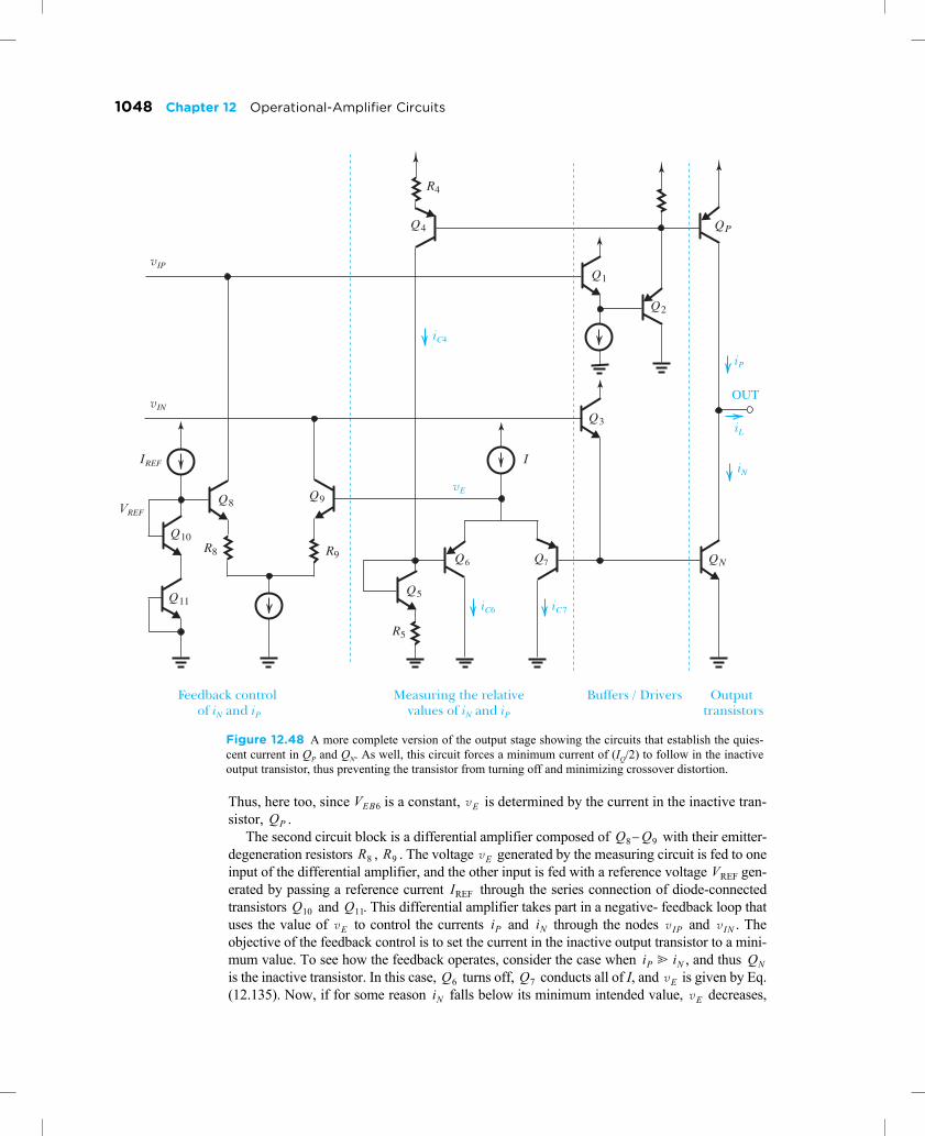
1048 Chapter 12 Operational-Amplifier Circuits
Thus, here too, since is a constant, is determined by the current in the inactive tran-sistor, .
The second circuit block is a differential amplifier composed of with their emitter-degeneration resistors , . The voltage generated by the measuring circuit is fed to oneinput of the differential amplifier, and the other input is fed with a reference voltage gen-erated by passing a reference current through the series connection of diode-connectedtransistors and . This differential amplifier takes part in a negative- feedback loop thatuses the value of to control the currents and through the nodes and . Theobjective of the feedback control is to set the current in the inactive output transistor to a mini-mum value. To see how the feedback operates, consider the case when , and thus is the inactive transistor. In this case, turns off, conducts all of I, and is given by Eq.(12.135). Now, if for some reason falls below its minimum intended value, decreases,
Q1
Q2
Q3
Q5
QP
QNR9
R5
R8
iC6
iC4
iC7
Q4
R4
iP
iN
iL
IREF
vIN
I
vE
vIP
VREF
Q8
Q10
Q11
Q9
Q7Q6
OUT
Feedback control of iN and iP
Measuring the relativevalues of iN and iP
Buffers / Drivers Output transistors
Figure 12.48 A more complete version of the output stage showing the circuits that establish the quies-cent current in QP and QN. As well, this circuit forces a minimum current of (IQ/2) to follow in the inactiveoutput transistor, thus preventing the transistor from turning off and minimizing crossover distortion.
VEB6 vEQP
Q8 Q9–R8 R9 vE
VREFIREF
Q10 Q11vE iP iN vIP vIN
iP � iN QNQ6 Q7 vE
iN vE

12.7 Modern Techniques for the Design of BJT Op Amps 1049
causing to decrease. This in turn will cause the node to rise and the voltage at the baseof will eventually rise, thus increasing to its intended value.
Analytically, we can obtain a relationship between and as follows. Assume that theloop gain of the feedback loop that is anchored by the differential amplifier is highenough to force the two input terminals to the same voltage, that is,
Substituting for from Eq. (12.134) results in
(12.137)
Observe that the quantity on the right-hand side is a constant. In the quiescent case,, Eq. (12.137) yields
(12.138)
Thus, the constant on the right-hand side of Eq. (12.137) is , and we can rewrite(12.137) as
(12.139)
Equation (12.139) clearly shows that for , , and that for , Thus the circuit not only establishes the quiescent current (Eq. 12.138) but also sets theminimum current in the inactive output transistor at
iC9 vINQN iN
iN iPQ8 Q9–
vE VREF VT ln IREF
IS10--------- VT ln
IREF
IS11---------+==
vE
iN iP
iN iP+---------------
IREF2
I---------⎝ ⎠⎛ ⎞ ISN
IS10--------⎝ ⎠⎛ ⎞ IS7
IS11--------⎝ ⎠⎛ ⎞=
iN iP IQ==
IQ 2IREF
2
I---------⎝ ⎠⎛ ⎞ ISN
IS10--------⎝ ⎠⎛ ⎞ IS7
IS11--------⎝ ⎠⎛ ⎞=
IQ 2⁄
iN iP
iN iP+--------------- 1
2---IQ=
iN � iP iP � 12---IQ iP � iN iN � 1
2---IQ.
IQ12---IQ.
D12.31 For the circuit in Fig. 12.48, determine the value that should have so that and havea quiescent current . Assume that the transistor areas are scaled so that
and . Let I = 10 μA. Also, if in the direction out of the amplifieris 10 mA, find and Ans.
IREF QN QPIQ 0.4 mA=
ISN IS10⁄ 10= IS7 IS11⁄ 2= iLiP iN.
IREF 10 μA;= iP � 10.2 mA, iN � 0.2 mA
EXERCISE

1050 Chapter 12 Operational-Amplifier Circuits
Summary
Most CMOS op amps are designed to operate as part ofa VLSI circuit and thus are required to drive only smallcapacitive loads. Therefore, most do not have a low-out-put-resistance stage.
There are basically two approaches to the design ofCMOS op amps: a two-stage configuration and a single-stage topology utilizing the folded-cascode circuit.
In the two-stage CMOS op amp, approximately equalgains are realized in the two stages.
The threshold mismatch ΔVt together with the low trans-conductance of the input stage result in a larger inputoffset voltage for CMOS op amps than for bipolar units.
Miller compensation is employed in the two-stageCMOS op amp, but a series resistor is required to placethe transmission zero at either s = ∞ or on the negativereal axis.
CMOS op amps have higher slew rates than their bipo-lar counterparts with comparable f t values.
Use of the cascode configuration increases the gain of aCMOS amplifier stage by about two orders of magni-tude, thus making possible a single-stage op amp.
The dominant pole of the folded-cascode op amp is de-termined by the total capacitance at the output node, CL.Increasing CL improves the phase margin at the expenseof reducing the bandwidth.
By using two complementary input differential pairs inparallel, the input common-mode range can be extendedto equal the entire power-supply voltage, providing so-called rail-to-rail operation at the input.
The output voltage swing of the folded-cascode op ampcan be extended by utilizing a wide-swing current mir-ror in place of the cascode mirror.
The internal circuit of the 741 op amp embodies manyof the design techniques employed in bipolar analog in-tegrated circuits.
The 741 circuit consists of an input differential stage, ahigh-gain single-ended second stage, and a class ABoutput stage. Though 40 years old, this structure is typ-ical of most BJT op amps and is known as the two-stagetopology (not counting the output stage). It is also thesame structure used in the two-stage CMOS op amp ofSection 12.1.
To obtain low input offset voltage and current, andhigh CMRR, the 741 input stage is designed to be per-fectly balanced. The CMRR is increased by common-mode feedback, which also stabilizes the dc operatingpoint.
To obtain high input resistance and low input bias current,the input stage of the 741 is operated at a very low currentlevel.
In the 741, output short-circuit protection is accom-plished by turning on a transistor that takes away mostof the base current drive of the output transistor.
The use of Miller frequency compensation in the 741circuit enables locating the dominant pole at a very lowfrequency, while utilizing a relatively small compensat-ing capacitance.
Two-stage op amps can be modeled as a transconduc-tance amplifier feeding an ideal integrator with CC asthe integrating capacitor.
The slew rate of a two-stage op amp is determined by thefirst-stage bias current and the frequency-compensationcapacitor.
While the 741 and its generation of op amps nominallyoperate from -V power supplies, modern BJT opamps typically utilize a single ground-referenced supplyof only 2 V to 3 V.
Operation from a single low-voltage supply gives rise toa number of new important specifications including acommon-mode input range that extends beyond the sup-ply rails (i.e., more than rail-to-rail operation) and a nearrail-to-rail output voltage swing.
The rail-to-rail input common-mode range is achieved byusing resistive loads (instead of current-mirror loads) forthe input differential pair as well as utilizing two comple-mentary differential amplifiers in parallel.
To increase the gain of the input stage above thatachieved with resistive loads, the folded-cascode config-uration is utilized.
To regulate the dc bias voltages at the outputs of the dif-ferential folded-cascode stage so as to maintain active-mode operation at all times, common-mode feedback isemployed.
The output stage of a low-voltage op amp utilizes acomplementary pair of common-emitter transistors.This allows to swing to within 0.1 V or so fromeach of the supply rails. The disadvantage is a highopen-loop output resistance. This, however, is sub-stantially reduced when negative feedback is appliedaround the op amp.
Modern output stages operate in the class AB mode andutilize interesting feedback techniques to set the quies-cent current as well as to ensure that the inactive outputtransistor does not turn off, a precaution that avoids in-creases in crossover distortion.
15±
vO

PROBLEMS
Computer Simulation Problems
Problems identified by this icon are intended to dem-onstrate the value of using SPICE simulation to verify handanalysis and design, and to investigate important issues suchas allowable signal swing and amplifier nonlinear distortion.Instructions to assist in setting up PSpice and Multism simu-lations for all the indicated problems can be found in thecorresponding files on the CD. Note that if a particularparameter value is not specified in the problem statement,you are to make a reasonable assumption.* difficult problem; ** more difficult; *** very challengingand/or time-consuming; D: design problem.
Section 12.1: The Two-Stage CMOS Op Amp
12.1 A particular design of the two-stage CMOS opera-tional amplifier of Fig. 12.1 utilizes ±1-V power supplies.All transistors are operated at overdrive voltages of 0.15-Vmagnitude. The process technology provides devices with
= 0.45 V. Find the input common-mode rangeand the range allowed for vO.
12.2 The CMOS op amp of Fig. 12.1 is fabricated in a pro-cess for which = 25 and = 20 . FindA1, A2, and Av if all devices are 0.5-μm long and are operated atequal overdrive voltages of 0.2-V magnitude. Also, determinethe op-amp output resistance obtained when the second stage isbiased at 0.4 mA. What do you expect the output resistance of aunity-gain voltage amplifier to be, using this op amp?
D 12.3 The CMOS op amp of Fig. 12.1 is fabricated in aprocess for which for all devices is 24 . If alltransistors have L = 0.5 μm and are operated at equal over-drive voltages, find the magnitude of the overdrive voltagerequired to obtain a dc open-loop gain of 6400 .
12.4 This problem is identical to Problem 8.107.
Consider the circuit in Fig. 12.1 with the device geome-tries shown at the bottom of this page. Let IREF = 225 μA,
for all devices = 0.75 V, μnCox = 180 μpCox =60 for all devices = 9 V, VDD = VSS = 1.5 V.Determine the width of Q6, W, that will ensure that the opamp will not have a systematic offset voltage. Then, forall devices, evaluate ID, , , gm, and ro. Provideyour results in a table. Also find A1, A2, the dc open-loopvoltage gain, the input common-mode range, and the out-put voltage range. Neglect the effect of VA on the biascurrents.
D 12.5 Design the two-stage CMOS op amp in Fig. 12.1 toprovide a CMRR of about 80 dB. If all the transistors areoperated at equal overdrive voltages of 0.15 V and haveequal channel lengths, find the minimum required channellength. For this technology, V/μm.
D 12.6 A particular implementation of the CMOSamplifier of Figs. 12.1 and 12.2 provides Gm1 = 0.3 mA/V,Gm2 = 0.6 mA/V, ro2 = ro4 = 222 kΩ, ro6 = ro7 = 111 kΩ,and C2 = 1 pF.
(a) Find the frequency of the second pole, fP2.(b) Find the value of the resistance R which when placed inseries with CC causes the transmission zero to be located ats = ∞.(c) With R in place, as in (b), find the value of CC thatresults in the highest possible value of ft while providing aphase margin of 80°. What value of ft is realized? What isthe corresponding frequency of the dominant pole?(d) To what value should CC be changed to double the valueof ft? At the new value of ft , what is the phase shift intro-duced by the second pole? To reduce this excess phase shiftto 10° and thus obtain an 80° phase margin, as before, whatvalue should R be changed to?
D 12.7 A two-stage CMOS op amp similar to that in Fig.12.1 is found to have a capacitance between the outputnode and ground of 0.5 pF. If it is desired to have a unity-gain bandwidth ft of 150 MHz with a phase margin of 75°what must gm6 be set to? Assume that a resistance R is con-nected in series with the frequency-compensation capaci-tor CC and adjusted to place the transmission zero atinfinity. What value should R have? If the first stage isoperated at = 0.15 V, what is the value of slew rateobtained? If the first-stage bias current I = 100 μA, whatis the required value of CC?
D 12.8 A CMOS op amp with the topology shown in Fig.12.1 is designed to provide mA/V and mA.
(a) Find the value of that results in MHz.(b) What is the maximum value that can have whileachieving a phase margin?
D 12.9 A CMOS op amp with the topology shown in Fig.12.1 but with a resistance R included in series with CC isdesigned to provide Gm1 = 1 mA/V and Gm2 = 2 mA/V.
(a) Find the value of CC that results in ft = 100 MHz.(b) For R = 500 Ω, what is the maximum allowed value ofC2 for which a phase margin of at least 60° is obtained?
Vtn Vtp=
VAn′ V/μm V ′Ap V/μm
VA′ V/μm
V/V
Vt μA/V2,μA/V2, VA
VOV VGS
VA′ 20=
VOV
Gm1 1= Gm2 5=
CC ft 100=C2
70°
Transistor Q1 Q2 Q3 Q4 Q5 Q6 Q7 Q8
W/ L (μm/μm) 30/ 0.5 30/ 0.5 10/ 0.5 10/ 0.5 60/ 0.5 W/ 0.5 60/ 0.5 60/ 0.5

CH
AP
TE
R 1
2P
RO
BL
EM
S
1052 Chapter 12 Operational-Amplifier Circuits
12.10 A two-stage CMOS op amp resembling that in Fig.12.1 is found to have a slew rate of 60 and a unity-gainbandwidth ft of 50 MHz.
(a) Estimate the value of the overdrive voltage at which theinput-stage transistors are operating.(b) If the first-stage bias current I = 100 μA, what value ofCC must be used?(c) For a process for which μpCox = 50 μA/V2, what ratio applies for Q1 and Q2?
D 12.11 Sketch the circuit of a two-stage CMOS amplifierhaving the structure of Fig. 12.1 but utilizing NMOS transis-tors in the input stage (i.e., Q1 and Q2).
D 12.12 (a) Show that the of a CMOS two-stageop amp for which all transistors have the same channellength and are operated at equal is given by
(b) For , what is the minimum channel lengthrequired to obtain a of 80 dB? For the technologyavailable, V/μm.
Section 12.2: The Folded-Cascode Op Amp
D 12.13 If the circuit of Fig. 12.8 utilizes ±1.65-V powersupplies and the power dissipation is to be limited to 1 mW,find the values of IB and I. To avoid turning off the currentmirror during slewing, select IB to be 20% larger than I.
D 12.14 For the folded-cascode op amp in Fig. 12.9 utiliz-ing power supplies of ±1 V, find the values of VBIAS1, VBIAS2,and VBIAS3 to maximize the allowable range of VICM and vO.Assume that all transistors are operated at equal overdrivevoltages of 0.15 V. Assume for all devices is 0.45 V.Specify the maximum range of VICM and of vO.
D 12.15 For the folded-cascode op-amp circuit of Figs.12.8 and 12.9 with bias currents I = 96 μA and IB = 120 μA,and with all transistors operated at overdrive voltages of0.2 V, find the ratios for all devices. Assume that thetechnology available is characterized by = 400 and = 100 .
12.16 Consider a design of the cascode op amp of Fig. 12.9for which I = 96 μA and IB = 120 μA. Assume that all transis-tors are operated at = 0.2 V and that for all devices,
= 12 V. Find Gm, Ro, and Av . Also, if the op amp is con-nected in the feedback configuration shown in Fig. P12.16,find the voltage gain and output resistance of the closed-loopamplifier.
D 12.17 Consider the folded-cascode op amp of Fig.12.8 when loaded with a 10-pF capacitance. What should
the bias current I be to obtain a slew rate of at least 10? If the input-stage transistors are operated at over-
drive voltages of 0.2 V, what is the unity-gain bandwidthrealized? If the two nondominant poles have the same fre-quency of 25 MHz, what is the phase margin obtained? Ifit is required to have a phase margin of 75°, what must ft
be reduced to? By what amount should CL be increased?What is the new value of SR?
D 12.18 Design the folded-cascode circuit of Fig. 12.9 toprovide voltage gain of 80 dB and a unity-gain frequency of10 MHz when CL = 10 pF. Design for IB = I, and operate alldevices at the same . Utilize transistors with 1-μmchannel length for which is specified to be 20 V. Findthe required overdrive voltages and bias currents. Whatslew rate is achieved? Also, for = 2.5 = 200specify the required width of each of the 11 transistorsused.
D 12.19 Sketch the circuit that is complementary to thatin Fig. 12.9, that is, one that uses an input p-channel dif-ferential pair.
12.20 For the circuit in Fig. 12.11, assume that all transis-tors are operating at equal overdrive voltages of 0.2-V mag-nitude and have = 0.5 V and that VDD = VSS = 1.65 V.Find (a) the range over which the NMOS input stage oper-ates, (b) the range over which the PMOS input stage oper-ates, (c) the range over which both operate (the overlaprange), and (d) the input common-mode range.
12.21 A particular design of the wide-swing current mirrorof Fig. 12.12(b) utilizes devices having = 25, = 200μA/V2, and Vt = 0.5 V. For IREF = 100 μA, what value of VBIAS
is needed? Also give the voltages that you expect to appearat all nodes and specify the minimum voltage allowable atthe output terminal. If VA is specified to be 10 V, what is theoutput resistance of the mirror?
D 12.22 For the folded-cascode circuit of Fig. 12.8, letthe total capacitance to ground at each of the source nodesof Q3 and Q4 be denoted CP. Assuming that the incrementalresistance between the drain of Q3 and ground is small,Show that the pole that arises at the interface between the
V/μs
W L⁄
PSRR–
VOV
PSRR– 2 VA
VOV---------
2=
VOV 0.2 V=PSRR–
VA′ 20=
Vt
W L⁄kn′ μA/V2
kp′ μA/V2
VOVVA
C
9C
Vi
Vo
Rof
�
�
Figure P12.16
V/μs
VOVVA
kn′ kp′ μA/V2,
Vt
W L⁄ k′n

Problems 1053
CH
AP
TE
R 1
2P
RO
BL
EM
S
first and second stages has a frequency .Now, if this is the only nondominant pole, what is thelargest value that CP can be (expressed as a fraction of CL )while a phase margin of 75° is achieved? Assume that alltransistors are operated at the same bias current and over-drive voltage.
Section 12.3: The 741 Op-Amp Circuit
12.23 In the 741 op-amp circuit of Fig. 12.13, Q1, Q2, Q5,and Q6 are biased at collector currents of 9.5 μA; Q16 isbiased at a collector current of 16.2 μA; and Q17 is biased ata collector current of 550 μA. All these devices are of the“standard npn” type, having IS = 10–14 A, β = 200, and VA =125 V. For each of these transistors, find VBE, gm, re, rπ, andro. Provide your results in table form. (Note that theseparameter values are utilized in the text in the analysis ofthe 741 circuit.)
D 12.24 For the (mirror) bias circuit shown in Fig.E12.11 and the result verified in the associated exercise,find I1 for the case in which IS3 = 3 × 10–14 A, IS4 = 6 × 10–14
A, and IS1 = IS2 = 10–14 A and for which a bias current I3 =154 μA is required.
12.25 Transistor Q13 in the circuit of Fig. 12.13 consists,in effect, of two transistors whose emitter–base junctionsare connected in parallel and for which ISA = 0.25 × 10⁻¹⁴ A,ISB = 0.75 × 10⁻¹⁴ A, β = 50, and VA = 50 V. For operation ata total emitter current of 0.73 mA, find values for the param-eters VEB, gm, re, rπ , and ro for the A and B devices.
12.26 In the circuit of Fig. 12.13, Q1 and Q2 exhibitemitter–base breakdown at 7 V, while for Q3 and Q4 such abreakdown occurs at about 50 V. What differential inputvoltage would result in the breakdown of the input-stagetransistors?
D *12.27 Figure P12.27 shows the CMOS version of thecircuit in Fig. E12.11. Find the relationship between I3 andI1 in terms of k1, k2, k3, and k4 of the four transistors, assum-ing the threshold voltages of all devices to be equal inmagnitude. Note that k denotes . In the event thatk1 = k2 and k3 = k4 = 16k1, find the required value of I1 toyield a bias current in Q3 and Q4 of 1.6 mA.
Section 12.4: DC Analysis of the 741
D 12.28 For the 741 circuit, estimate the input referencecurrent IREF in the event that ±5-V supplies are used. Find amore precise value assuming that for the two BJTs involved,IS = 10–14 A. What value of R5 would be necessary to rees-tablish the same bias current for ±5-V supplies as exists for±15 V in the original design?
D 12.29 Design the Widlar current source of Fig. 12.14 togenerate a current IC10 = 10 μA given that IREF = 0.2 mA. Iffor the transistors, IS = 10–14 A, find VBE11 and VBE10. Assumeβ to be high.
12.30 Consider the dc analysis of the 741 input stageshown in Fig. 12.15. For what value of βP do the currents inQ1 and Q2 differ from the ideal value of IC10 / 2 by 10%?
D 12.31 Consider the dc analysis of the 741 input stageshown in Fig. 12.15 for the situation in which IS9 = 2IS8. For IC10
= 19 μA and assuming βP to be high, what does I become?Redesign the Widlar source to reestablish IC1 = IC2 = 9.5 μA.
12.32 For the mirror circuit shown in Fig. 12.16 with thebias and component values given in the text for the 741 cir-cuit, what does the current in Q6 become if R2 is shorted?
D 12.33 It is required to redesign the circuit of Fig. 12.16by selecting a new value for R3 so that when the base cur-rents are not neglected, the collector currents of Q5, Q6, andQ7 all become equal, assuming that the input current IC3 =9.4 μA. Find the new value of R3 and the three currents.Recall that βN = 200.
12.34 Consider the input circuit of the 741 op amp of Fig.12.13 when the emitter current of Q8 is about 19 μA. If β ofQ1 is 150 and that of Q2 is 200, find the input bias current IB
and the input offset current IOS of the op amp.
12.35 For a particular application, consideration is beinggiven to selecting 741 ICs for input bias and offset currentslimited to 50 nA and 4 nA, respectively. Assuming other
fP � gm3 2πCP⁄
μCoxW/L
Figure P12.27

CH
AP
TE
R 1
2P
RO
BL
EM
S
1054 Chapter 12 Operational-Amplifier Circuits
aspects of the selected units to be normal, what minimum βN
and what βN variation are implied?
12.36 A manufacturing problem in a 741 op amp causesthe current transfer ratio of the mirror circuit that loads theinput stage to become 0.8 A/A. For input devices (Q1–Q4)appropriately matched and with high β, and normallybiased at 9.5 μA, what input offset voltage results?
D 12.37 Consider the design of the second stage of the741. What value of R9 would be needed to reduce IC16 to9.5 μA?
D 12.38 Reconsider the 741 output stage as shown in Fig.12.17, in which R10 is adjusted to make IC19 = IC18. What isthe new value of R10? What values of IC14 and IC20 result?
D *12.39 An alternative approach to providing the voltagedrop needed to bias the output transistors is the VBE –multiplier circuit shown in Fig. P12.39. Design the circuit toprovide a terminal voltage of 1.118 V (the same as in the 741circuit). Base your design on half the current flowing throughR1, and assume that IS = 10–14 A and β = 200. What is theincremental resistance between the two terminals of the VBE –multiplier circuit?
12.40 For the circuit of Fig. 12.13, what is the total cur-rent required from the power supplies when the op amp isoperated in the linear mode, but with no load? Hence, esti-mate the quiescent power dissipation in the circuit. (Hint:Use the data given in Table 12.1.)
Section 12.5: Small-Signal Analysis of the 741
12.41 Consider the 741 input stage as modeled in Fig.12.18, with two additional npn diode-connected transistors,Q1a and Q2a, connected between the present npn and pnp
devices, one per side. Convince yourself that each of theadditional devices will be biased at the same current as Q1 toQ4—that is, 9.5 μA. What does Rid become? What does Gm1
become? What is the value of Ro4 now? What is the outputresistance of the first stage, Ro1? What is the new open-circuit voltage gain, Gm1Ro1? Compare these values with theoriginal ones.
D 12.42 What relatively simple change can be made tothe mirror load of stage 1 to increase its output resistance,say by a factor of 2?
12.43 Repeat Exercise 12.15 with R1 = R2 replaced by 2-kΩresistors.
*12.44 In Example 12.3 we investigated the effect of amismatch between R1 and R2 on the input offset voltage ofthe op amp. Conversely, R1 and R2 can be deliberately mis-matched (using the circuit shown in Fig. P12.44, for example)to compensate for the op-amp input offset voltage.
(a) Show that an input offset voltage VOS can be compen-sated for (i.e., reduced to zero) by creating a relative mis-match ΔR/R between R1 and R2,
where re is the emitter resistance of each of Q1 to Q6, and Ris the nominal value of R1 and R2. (Hint: Use Eq. 12.87)(b) Find ΔR/R to trim a 5-mV offset to zero.(c) What is the maximum offset voltage that can betrimmed this way (corresponding to R2 completely shorted)?
12.45 Through a processing imperfection, the β of Q4 inFig. 12.13 is reduced to 20, while the β of Q3 remains at itsregular value of 50. Find the input offset voltage that thismismatch introduces. (Hint: Follow the general procedureoutlined in Example 12.3.)
I � 180 μA
180 μA
Figure P12.39
ΔRR
-------VOS
2VT---------
1 re R⁄+1 VOS 2VT⁄–-------------------------------=
Figure P12.44

Problems 1055
CH
AP
TE
R 1
2P
RO
BL
EM
S
12.46 Consider the circuit of Fig. 12.13 modified toinclude resistors R in series with the emitters of each of Q8
and Q9. What does the resistance looking into the collector ofQ9, Ro9, become? For what value of R does it equal Ro10? Forthis case, what does Ro looking to the left of node Y become?
*12.47 What is the effect on the differential gain of the741 op amp of short-circuiting one, or the other, or both, ofR1 and R2 in Fig. 12.13? (Refer to Fig. 12.19.) For simplic-ity, assume β = ∞.
12.48 It is required to show that the loop gain of the com-mon-mode feedback loop shown in Fig. 12.23 is approxi-mately equal to . To determine the loop gain, connectboth input terminals to ground. Break the loop at the input tothe current mirror, connecting the collec-tors to signal ground. (This is because the original resistancebetween the collectors and ground is , which is small.)Apply a test current to and determine the returnedcurrent in the common collectors’ connection to ground,then find the loop gain as . Assume that of Q1 toQ4 is much lower than and that , .
12.49 An alternative approach to that presented in Exam-ple 12.4 for determining the CMRR of the 741 input stage isinvestigated in this problem. Rather than performing theanalysis on the closed loop shown in Fig. 12.23, we observethat the negative feedback increases the resistance at node Yby the amount of negative feedback. Thus, we can break theloop at Y and connect a resistance between the common base connection of andground. We can then determine the current i and .Using the fact that the loop gain is approximately equal to
(Problem 12.48) show that this approach yields an iden-tical result to that found in Example 12.4.
12.50 Consider a variation on the design of the 741 sec-ond stage in which R8 = 50 Ω. What Ri2 and Gm2 correspond?
12.51 In the analysis of the 741 second stage, note that Ro2
is affected most strongly by the low value of Ro13B. Considerthe effect of placing appropriate resistors in the emitters ofQ12, Q13A, and Q13B on this value. What resistor in the emitterof Q13B would be required to make Ro13B equal to Ro17 andthus Ro2 half as great? What resistors in each of the otheremitters would be required?
12.52 For a 741 employing ±5-V supplies, and , find the output voltage limits thatapply.
D 12.53 Consider an alternative to the present 741 outputstage in which Q23 is not used, that is, in which its base andemitter are joined. Reevaluate the reflection of RL = 2 kΩ tothe collector of Q17. What does A2 become?
12.54 Consider the positive current-limiting circuitinvolving Q13A, Q15, and R6. Find the current in R6 at whichthe collector current of Q15 equals the current available fromQ13A (180 μA) minus the base current of Q14. (You need toperform a couple of iterations.)
D 12.55 Consider the 741 sinking-current limit involv-ing R7, Q21, Q24, R11, and Q22. For what current through R7
is the current in Q22 equal to the maximum current avail-able from the input stage (i.e., the current in Q8)? Whatsimple change would you make to reduce this currentlimit to 10 mA?
Section 12.6: Gain, Frequency Response, and Slew Rate of the 741
12.56 Using the data provided in Eq. (12.112) (alone) forthe overall gain of the 741 with a 2-kΩ load, and realizingthe significance of the factor 0.97 in relation to the load, cal-culate the open-circuit voltage gain, the output resistance,and the gain with a load of 200 Ω.
12.57 A 741 op amp has a phase margin of 75°. If theexcess phase shift is due to a second single pole, what is thefrequency of this pole?
12.58 A 741 op amp has a phase margin of 75°. If the opamp has nearly coincident second and third poles, what istheir frequency?
D *12.59 For a modified 741 whose second pole is at 5MHz, what dominant-pole frequency is required for 80°phase margin with a closed-loop gain of 100? Assuming CC
continues to control the dominant pole, what value of CC
would be required?
12.60 An internally compensated op amp having an ft of10 MHz and dc gain of 106 utilizes Miller compensationaround an inverting amplifier stage with a gain of –1000. Ifspace exists for at most a 50-pF capacitor, what resistancelevel must be reached at the input of the Miller amplifier forcompensation to be possible?
12.61 Consider the integrator op-amp model shown inFig. 12.33. For Gm1 = 5 mA/V, CC = 100 pF, and a resis-tance of Ω shunting CC , sketch and label a Bodeplot for the magnitude of the open-loop gain. If Gm1 isrelated to the first-stage bias current as Gm1 = I/2VT , find theslew rate of this op amp.
12.62 For an amplifier with a slew rate of 10 V/μs, whatis the full-power bandwidth for outputs of ±10 V? Whatunity-gain bandwidth, ωt, would you expect if the topologywas similar to that of the 741?
βP
Q8 Q9– Q1 Q2–
re8It Q8
IrIr It⁄– rπ
Ro βN βP �1
Rf 1 Aβ+( )Ro=Q3 Q4–
Gmcm
βP
VBE 0.6 V=VCEsat 0.2 V=
2 107×

CH
AP
TE
R 1
2P
RO
BL
EM
S
1056 Chapter 12 Operational-Amplifier Circuits
D *12.63 Figure P12.63 shows a circuit suitable for op-amp applications. For all transistors β = 100, VBE = 0.7 V,and ro = ∞.
(a) For inputs grounded and output held at 0 V (by negativefeedback) find the collector currents of all transistors.Neglect base currents. (b) Calculate the input resistance.(c) Calculate the gain of the amplifier with a load of 5 kΩ.(d) With load as in (c) calculate the value of the capacitor Crequired for a 3-dB frequency of 100 Hz.
Section 12.7: Modern Techniques for the Design of BJT Op Amps
Unless otherwise specified, for the problems in this sectionassume , , V, V,
V, V.
D 12.64 Design the circuit in Fig. 12.38 to generate acurrent I = 6 μA. Utilize transistors and having areasin a ratio of 1:4. Assume that and are matched anddesign for a 0.2-V drop across each of and Specifythe values of and Ignore base currents.
D 12.65 Consider the circuit of Fig. 12.38 for the casedesigned in Exercise 12.28, namely, I = 10 μA,
, , . Aug-ment the circuit with npn transistors and with emit-ters connected to ground and bases connected to , to
generate constant currents of 10 μA and 40 μA, respectively.What should the emitter areas of and be relative tothat of ? What value of a resistance will, when con-nected in the emitter of , reduce the current generated by
to 10 μA? Assuming that the line has a low incre-mental resistance to ground, find the output resistance ofcurrent source and of current source with con-nected. Ignore base currents.
D 12.66 (a) Find the input common-mode range of thecircuit in Fig. 12.40(a). Let V and 2.3 V.
(b) Give the complementary version of the circuit in Fig.12.40(a), that is, the one in which the differential pair is npn.For the same conditions as in (a), what is the input common-mode range?
12.67 For the circuit in Fig. 12.40(b), let V, V, I = 20 μA, and . Find the input
common-mode range and the differential voltage gain. Neglect base currents.
12.68 For the circuit in Fig. 12.41, let V, V, and μA. Find that results in
a differential gain of 10 V/V. What is the input common-mode range and the input differential resistance? Ignorebase currents except when calculating .
12.69 It is required to find the input resistance and thevoltage gain of the input stage shown in Fig. 12.42. Let
V so that the pair is off. Assume that
Figure P12.63
βN 40= βP 10= VAn 30= VAp 20=VBE 0.7= VCEsat 0.1=
Q1 Q2Q3 Q4
R3 R4.R2, R3, R4.
IS2 IS1⁄ 2= R2 1.73 kΩ= R3 R4 20 kΩ==Q5 Q6
VBIAS1
Q5 Q6Q1 R6
Q6Q6 VBIAS1
Q5 Q6 R6
VCC 3= VBIAS =
VCC 3=VBIAS 2.3= RC 20 kΩ=
vo vid⁄
VCC 3=VBIAS 0.7= IC6 10= RC
Rid
VICM � 0.8 Q3 Q4–
Problems 1057
CH
AP
TE
R 1
2P
RO
BL
EM
S
supplies 6 μA, that each of to is biased at 6 μA,and that all four cascode transistors are operating in theactive mode. The input resistance of the second stage of theop amp is 1.3 M . The emitter degeneration resistances are
k , and k . [Hint: Referto Fig. 12.43.]
D 12.70 Consider the equivalent half-circuit shown inFig. 12.43. Assume that in the original circuit, isbiased at a current I, and are biased at 2I, the dcvoltage drop across is 0.2 V, and the dc voltage dropacross is 0.3 V. Find the open-circuit voltage gain(i.e., the voltage gain for ). Also find the outputresistance in terms of I. Now with connected, find thevoltage gain in terms of . For , find Ithat will result in the voltage gains of 160 V/V and320 V/V.
*12.71 (a) For the circuit in Fig. 12.44, show that the loopgain of the common-mode feedback loop is
Recall that the CMF circuit realizes the transfer characteris-tic . Ignore the loading effect of the CMFcircuit on the collectors of the cascode transistors. (b) For the values in Example 12.6, calculate the loop gain
.(c) In Example 12.6, we found that with the CMF absent, acurrent mismatch μA gives rise to V.Now, with the CMF present, use the value of loop gain foundin (b) to calculate the expected and compare to thevalue found by a different approach in Example 12.6. [Hint:Recall that negative feedback reduces change by a factorequal to .]
12.72 The output stage in Fig. 12.46 operates at a quiescentcurrent of 0.4 mA. The maximum current that the stagecan provide in either direction is 10 mA. Also, the output stage
is equipped with a feedback circuit that maintains a minimumcurrent of in the inactive output transistor.
(a) What is the allowable range of (b) For , what is the output resistance of the op amp?(c) If the open-loop gain of the op amp is 100,000 V/V, findthe closed-loop output resistance obtained when the op ampis connected in the unity-gain voltage follower configura-tion, with (d) If the op amp is sourcing a load current find and the open-loop output resistance.(e) Repeat (d) for the case of the open-loop op amp sinking aload current of 10 mA.
12.73 It is required to derive the expressions in Eqs. (12.132)and (12.133). Toward that end, first find in terms of and hence Then find in terms of For the latter pur-pose note that measures and develops a current
. This current is supplied to the seriesconnection of and where In the expressionyou obtain for use the relationship
to express in terms of and Now with and determined, find and
12.74 It is required to derive the expression for in Eq.(12.134). Toward that end, note from the circuit in Fig.12.48 that and note that conducts acurrent and conducts a current given by Eq.(12.133).
D 12.75 For the output stage in Fig. 12.48, find the cur-rent that results in a quiescent current
Assume that I = 10 μA, has eighttimes the area of , and has four times the area of .What is the minimum current in and
Q5 Q7 Q10
ΩR7 R8 22== Ω R9 R10 33== Ω
Q1Q7 Q9
R7R9
RL ∞=RL
IRL( ) RL 2 MΩ=
Aβ � Ro9 Ro7||re7 R7+----------------------
VB VCM 0.4+=
Aβ
I 0.3=Δ VCM 2.5=Δ
VCMΔ
1 Aβ+( )
IQ iL
IQ 2⁄
vO?iL 0=
iL 0.=iL 10 mA,=
iP, iN,
vB7 vBENiN. vB6 iP.
Q4 vEBPi4 vEBP vEB4–( ) R4⁄=
Q5 R5 R5 R4.=vB6,
ISP
IS4------- ISN
IS5-------=
vB6 iP ISN. vB6vB7 iC6 iC7.
vE
vE vEB7 vBEN+= QNiN Q7 iC7
IREFIQ 0.36 mA.= QN
Q10 Q7 Q11QN QP?