ON Semiconductor Solutions for Smart Phones and Tablets
52
-
Upload
khangminh22 -
Category
Documents
-
view
0 -
download
0
Transcript of ON Semiconductor Solutions for Smart Phones and Tablets

Page 2 Portable Solutions
ON Semiconductor Solutions for Smart Phones and Tablets
Modular product architectures have largely ‘leveled the playing field’ in the wireless device industry. Increasingly, hardware manufacturers have broadly similar access to operating systems and chipset platforms. In order to be successful in this environment, device manufacturers must work quickly to introduce differentiated hardware, providing innovative features on top of the chipset platform.
ON Semiconductor provides a broad portfolio of building block solutions that enable rapid hardware differentiation, enabling additional features with components for power management, RF, display, LED, audio, interface, and protection.
Subsystem Power Supplies
Memory
Audio
Touch Display& UI
Camera
Building Block Components
BatteryPack
WirelessCharging
PowerManagementUnit (PMU)
ApplicationsProcessor
CoreDC-DC
TempSensor
Vbat
Vbat
USB
Vbat
RAM
ALS + Proximity Sensor
Camera PMIC
WLAN/BT/FM/GPS/NFC Module
Smart Phone
Mass Storage
EEPROM
BatteryCharger
USBProtection
PowerProtection
CODEC
SpeechDSP
AudioProtection
DisplayDriver
DisplayProtection
SIM/MemoryCard Interface
TouchController
AMOLEDPower
LCDDisplay
MotorHaptics MotorDriver
LEDBacklight
Lens AFDriver
CameraEEPROM
CameraProtection
Active EMISuppression
ClockGeneration
CellularModem SoC
TunableRF
PADC-DC
Front EndModule
MEMsSensors
Lens
FlashOIS FlashDriver
USB/MHLSwitches
PowerAdapter
Small SignalDiscretes
Switches &Op Amps
StandardLogic
ESD/EMIProtection
PowerDiscretesLDOMini
PMIC
LoadSwitchDC-DC
SpeakerAmp
HeadPhoneAmp
PA
Page 3ON Semiconductor
POW
ER M
ANAG
EMEN
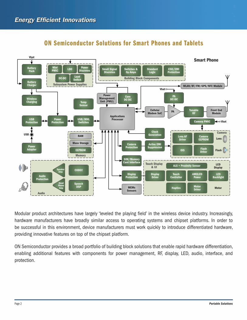
TARM® Core DC-DC ConvertersKey Features• High regulating performance from 0.6 V to 1.4 V
• Modular efficiency with fragmented power stage• Dynamic voltage scaling per output steps of 6.25 mV by I2C• Tight accuracy of ±1%, due to differential sensing
• Fast transient response• Proprietary PFM to PWM transition with equivalent performance to PWM only• Thermally handle high peak current demands up to 10 ms• Flexible design to transient handling output capacitor from 22 µF to 100 µF
DeviceVIN(V)
VOUT(V)
IOUT(A)
fSW(MHz) Control Features Package
NCP6338 2.3 – 5.5 0.6 – 1.4 6.0 3.0 I²C; VSEL Modular power stage; Differential sensing WLCSP-30
NCP6335 2.3 – 5.5 0.6 – 1.4 4.0 3.0 I²C; VSEL Transient load helper WLCSP-20
NCP6343* 2.3 – 5.5 0.6 – 1.4 3.5 3.0 I²C Dynamic voltage scaling WLCSP-15
NCP6342* 2.3 – 5.5 0.6 – 1.4 2.5 3.0 I²C Dynamic voltage scaling WLCSP-12
* Pending 2H13.
0.95
0.9
0.85
0.8
0.75
0.70.10 1.00
Effici
ency
(%)
Load Current (A)
PWM Efficiency DCDC Converter Modular OutputVin = 3.6 V, Vout = 1.20 V, Fsw = 3.0 MHz, Lossless Inductor(s)
Number of Modules
1 2 3 5 10

Page 4 Portable Solutions
POW
ER M
ANAG
EMEN
T
Peripheral DC-DC Converters
Key Features• High efficiency conversion - up to 94% - over large input &
output voltage range• High switching frequency - up to 6.0 MHz - reduces external
component size (inductor down to 220 nH)• Design flexibility with adjustable resistor bridge, independent
enable control, power good or mode selection pin
DeviceVIN(V)
VOUT(V)
IOUT(A)
fSW(MHz) Operating Mode Features Package(s)
NCP1521B 2.7 – 5.5 0.9 – 3.3 0.6 1.5 PFM/PWM - TSOP-5, UDFN-6
NCP1522B 2.7 – 5.5 0.9 – 3.3 0.6 3 PFM/PWM - TSOP-5, UDFN-6
NCP1529 2.7 – 5.5 0.9 – 3.3 1.0 1.7 PFM/PWM - TSOP-5, UDFN-6
NCP6332B 2.3 – 5.5 0.6 – 5.0 1.2 3 PFM/PWM Power Good UDFN-8
NCP6332C 2.3 – 5.5 0.6 – 5.0 1.2 3 PFM/PWM Mode Selection UDFN-8
NCP6334B 2.3 – 5.5 0.6 – 5.0 2.0 3 PFM/PWM Power Good UDFN-8
NCP6334C 2.3 – 5.5 0.6 – 5.0 2.0 3 PFM/PWM Mode Selection UDFN-8
NCP6354 2.3 – 5.5 0.6 – 5.0 2.0 3 PWM Power Good UDFN-8
PVINCore
SW
FB
PGND
AVINBattery orSystem Supply
Battery orSystem Supply
DCDC Out
10 μF
22 μF
1 μH
Processor orSystem Supply
Power StateIndicator
AGND
EN
PG
DCDC
2 A1.5-6 MHz
ThermalProtection
Enabling
Control
Power Good (B version) Limit external component countMode Selection (C version) Design flexibility
Small inductor down to 220 nHSmall capacitor: 10 μF Cost and space savings
50
55
60
65
70
75
80
85
90
95
100
1 10 100 1000 10000
Effici
ency
(%)
Output Current (mA)
NCP6314C auto mode, Vout = 1.8 V
2.7 V
3.6 V
5.5 V
Page 5ON Semiconductor
POW
ER M
ANAG
EMEN
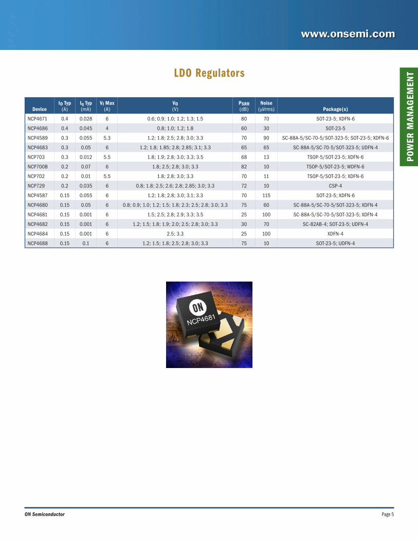
TLDO Regulators
DeviceIO Typ
(A) Iq Typ(mA)
VI Max(A)
VO(V)
PSRR(dB)
Noise(mVrms) Package(s)
NCP4671 0.4 0.028 6 0.6; 0.9; 1.0; 1.2; 1.3; 1.5 80 70 SOT-23-5; XDFN-6
NCP4686 0.4 0.045 4 0.8; 1.0; 1.2; 1.8 60 30 SOT-23-5
NCP4589 0.3 0.055 5.3 1.2; 1.8; 2.5; 2.8; 3.0; 3.3 70 90 SC-88A-5/SC-70-5/SOT-323-5; SOT-23-5; XDFN-6
NCP4683 0.3 0.05 6 1.2; 1.8; 1.85; 2.8; 2.85; 3.1; 3.3 65 65 SC-88A-5/SC-70-5/SOT-323-5; UDFN-4
NCP703 0.3 0.012 5.5 1.8; 1.9; 2.8; 3.0; 3.3; 3.5 68 13 TSOP-5/SOT-23-5; XDFN-6
NCP700B 0.2 0.07 6 1.8; 2.5; 2.8; 3.0; 3.3 82 10 TSOP-5/SOT-23-5; WDFN-6
NCP702 0.2 0.01 5.5 1.8; 2.8; 3.0; 3.3 70 11 TSOP-5/SOT-23-5; XDFN-6
NCP729 0.2 0.035 6 0.8; 1.8; 2.5; 2.6; 2.8; 2.85; 3.0; 3.3 72 10 CSP-4
NCP4587 0.15 0.055 6 1.2; 1.8; 2.8; 3.0; 3.1; 3.3 70 115 SOT-23-5; XDFN-6
NCP4680 0.15 0.05 6 0.8; 0.9; 1.0; 1.2; 1.5; 1.8; 2.3; 2.5; 2.8; 3.0; 3.3 75 60 SC-88A-5/SC-70-5/SOT-323-5; XDFN-4
NCP4681 0.15 0.001 6 1.5; 2.5; 2.8; 2.9; 3.3; 3.5 25 100 SC-88A-5/SC-70-5/SOT-323-5; XDFN-4
NCP4682 0.15 0.001 6 1.2; 1.5; 1.8; 1.9; 2.0; 2.5; 2.8; 3.0; 3.3 30 70 SC-82AB-4; SOT-23-5; UDFN-4
NCP4684 0.15 0.001 6 2.5; 3.3 25 100 XDFN-4
NCP4688 0.15 0.1 6 1.2; 1.5; 1.8; 2.5; 2.8; 3.0; 3.3 75 10 SOT-23-5; UDFN-4
Page 6 Portable Solutions
POW
ER M
ANAG
EMEN
T
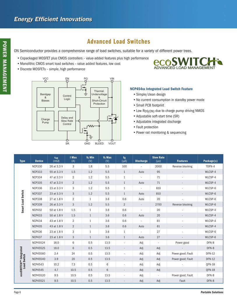
Advanced Load Switches
• Copackaged MOSFET plus CMOS controllers – value-added features plus high performance• Monolithic CMOS smart load switches – value added features, low cost• Discrete MOSFETs – simple, high performance
ON Semiconductor provides a comprehensive range of load switches, suitable for a variety of different power trees.
NCP454xx Integrated Load Switch Feature• Simple/clean design• No current consumption in standby power mode• Small PCB footprint• Low RDS(ON) due to charge pump driving NMOS• Adjustable soft-start time (SR)• Adjustable integrated discharge• Fault protection• Power rail monitoring & sequencing
Thermal,Undervoltage
&Short-CircuitProtection
ControlLogic
Bandgap&
Biases
Delay andSlew Rate
Control
ChargePump
VIN
VOUTBLEEDGNDSR
PGENVCC
Type Deviceron
(mW) I Max
(A) VI Min
(V) VI Max
(V) IQ
(mA) DischargeSlew Rate
(ms) Features Package(s)
Smar
t Loa
d Sw
itch
NCP330 26 at 3.3 V 3 1.8 5.5 100 - 2000 Reverse blocking TDFN-4
NCP333 55 at 3.3 V 1.5 1.2 5.5 1 Auto 95 - WLCSP-4
NCP334 47 at 3.3 V 2 1.2 5.5 1 - 71 - WLCSP-4
NCP335 47 at 3.3 V 2 1.2 5.5 1 Auto 71 - WLCSP-4
NCP336 23 at 3.3 V 3 1.2 5.5 1 - 810 - WLCSP-6
NCP337 23 at 3.3 V 3 1.2 5.5 1 Auto 810 - WLCSP-6
NCP338 27 at 1.8 V 2 1 3.6 0.6 Auto 20 - WLCSP-6
NCP339 26 at 3.3 V 3 1.2 5.5 2 - 2700 Reverse blocking WLCSP-6
NCP432 50 at 1.8 V 1.5 1 3.6 0.6 - 20 - WLCSP-4
NCP433 50 at 1.8 V 1.5 1 3.6 0.6 Auto 20 - WLCSP-4
NCP434 43 at 1.8 V 2 1 3.6 0.6 - 61 - WLCSP-4
NCP435 43 at 1.8 V 2 1 3.6 0.6 Auto 61 - WLCSP-4
NCP436 23 at 1.8 V 3 1 3.6 1 - 27 - WLCSP-6
NCP437 23 at 1.8 V 3 1 3.6 1 Auto 27 - WLCSP-6
ecoS
WIT
CH™
Inte
grat
ed
Load
Sw
itch
NCP45524 18.0 6 0.5 13.5 - Adj - Power good DFN-8
NCP45525 18.0 6 0.5 13.5 - Adj Adj - DFN-8
NCP45560 2.4 24 0.5 13.5 - Adj Adj Power good; Fault DFN-12
NCP45540 3.9 20 0.5 13.5 - Adj Adj Power good; Fault DFN-12
NCP4543 10.2 7.3 0.5 6 - Adj Adj - QFN-18
NCP4545 4.7 10.5 0.5 6 - Adj Adj - QFN-18
NCP45520 9.5 10.5 0.5 13.5 - Adj - Power good; Fault DFN-8
NCP45521 9.5 10.5 0.5 13.5 - Adj Adj Fault DFN-8

Page 7ON Semiconductor
POW
ER M
ANAG
EMEN
TSimple Load Switches
Device Polarity ConfigurationV(BR)DSS Min
(V) VGS Max
(V) ID Max
(A) RDS(ON) Max @ VGS = 4.5 V
(W) Package(s)
EFC6301* P-Channel Single -12 ±8 -6 0.0215 EFCP
SCH1342* P-Channel Single -12 ±10 -4.5 0.041 SCH-6
SCH1345* P-Channel Single -20 ±10 -4.5 0.049 SCH-6
NTLUS3C18PZ* P-Channel Single -12 ±8 7 0.024 UDFN
NTLUS3A39PZ P-Channel Single -20 ±8 5.2 0.039 UDFN-6
NTLUD3A260PZ P-Channel Dual -20 ±8 1.7 0.2 UDFN-6
NTLUS3C13PZ* P-Channel Single -12 ±8 10 0.0125 UDFN
NTLUS3A18PZ P-Channel Single -20 ±8 8.2 0.018 UDFN-6
NTLUD3A50PZ P-Channel Dual -20 ±8 4.5 0.048 UDFN-6
NTLUS3A28PZ* P-Channel Single -30 ±25 8 0.028 UDFN
NTLJS3A18PZ P-Channel Single -20 ±8 8.2 0.018 WDFN-6
MCH6351* P-Channel Single -12 ±10 -9 0.0169 MCPH-6
EMH2314 P-Channel Dual -12 ±10 -5 0.037 EMH-8
ECH8308 P-Channel Single -12 ±10 -10 0.0125 ECH-8
NTTFS3A08PZ P-Channel Single -20 ±8 15 0.067 µ8FL
SCH1433 N-Channel Single 20 ±10 3.5 0.064 SCH-6
SCH1440* N-Channel Single 20 ±10 4.5 0.045 SCH-6
NTLUS4930N N-Channel Single 30 ±20 6.3 0.033 UDFN-6
NTLUS4C12N* N-Channel Single 30 ±20 9.1 0.015 UDFN
NTLJS4114N N-Channel Single 30 ±12 6 0.035 WDFN-6
NTLJD4116N N-Channel Dual 30 ±12 3.7 0.07 WDFN-6
MCH6448 N-Channel Single 20 ±9 8 0.022 MCPH-6
EMH1405 N-Channel Single 30 ±20 8.5 0.034 EMH-8
EMH2407 N-Channel Dual - Common Drain 20 ±12 6 0.025 EMH-8
EMH2408 N-Channel Dual 20 ±12 4 0.045 EMH-8
ECH8420 N-Channel Single 20 ±12 14 0.0068 ECH-8
ECH8656 N-Channel Dual 20 ±10 7.5 0.017 ECH-8
* Pending 2H13.
PMU/Charging ICMOSFET
Vin USB
System
SecondaryCharging Pass
(Wireless)
Switching Charger – Step Down

Page 8 Portable Solutions
POW
ER M
ANAG
EMEN
T
Switching Battery Chargers
Key Features• Sized for micro USB connector (USB BC1.2) with 1.5 A, 1.6 A, 1.8 A charging current• Automatic input current limit adapts charging current to the maximum capability of the power source;
proven charging time decrease by 10 minutes• Integrated 28 V over voltage protection with unique negative voltage support• Embedded 500 mA boost USB OTG saves
BOM cost• Automatically disconnects battery at end
of charge, with reconnect in few seconds in case of peak current activity (GSM for instance)
• Instant turn-on at cable insertion when battery is weak
Device
Charging Current Max
(A)
Pre-Charge Current Max
(mA)
OTG Boost Current Max
(mA)
VCC Max (V)
OVP(V) I2C
Automatic Input Current
LimitingDual Path
Management
Protected USB PHY
Supply (mA)
Battery Temperature
Sensing Package
NCP1850 1.5 450 250 7 +28 400 kHz Yes Yes (external) 30 Threshold WLCSP-25
NCP1851 1.6 300 500 7 +28 400 kHz / 3.4 MHz Yes Yes (external) 50 JEITA Flip-Chip-25
NCP1852 1.8 300 500 7 +28/–20 400 kHz / 3.4 MHz Yes Yes (external) 50 JEITA Flip-Chip-25
NCP1851 Charging Profile for 4.2 V, 1650 mAh Battery Pack
Current &Voltage
Monitoring
DynamicPower Path
Management
300 mAPrecharge
AutomaticInput Current
Limiter
BatteryCharging
StateMachine
JEITA ProfileOver Temp
Battery
NT
C
1.8 ASwitching
Battery Charger
+28 V / -20 VOvervoltageProtection
500 mA5 V Boost
NCP1852
USBTransceiver
Supply
I2C400 kHz3.4 MHz
0
1
2
3
4
5
6
0
0.2
0.4
0.6
0.8
1.0
1.2
1.4
1.6
1.8
0 1000 2000 3000 4000 5000 6000
Iin (mA)
Ibat (A)
Vbat (V)
Vin (V)
Page 9ON Semiconductor
POW
ER M
ANAG
EMEN
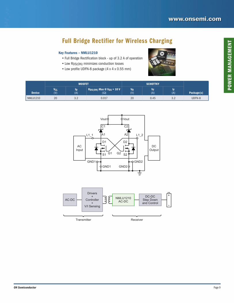
TFull Bridge Rectifier for Wireless Charging
Key Features – NMLU1210• Full Bridge Rectification block - up of 3.2 A of operation• Low RDS(ON) minimizes conduction losses• Low profile UDFN-8 package (4 x 4 x 0.55 mm)
Device
MOSFET SCHOTTKY
Package(s) VLL(V)
ID(A)
RDS(ON) Max @ VGS = 10 V (W)
VR(V)
VF(A)
IF(A)
NMLU1210 20 3.2 0.017 20 0.45 3.2 UDFN-8
D2
A2
C2
S2G2
D1
L1_1 A1
C1
S1 G1
GND1
GND1
ACInput
DCOutput
L1_2
GND2
GND2
Vout Vout
NMLU1210AC-DC
DC-DCStep Downand Control
AC-DC
Transmitter Receiver
Drivers+
Controller+
V/I Sensing

Page 10 Portable Solutions
POW
ER M
ANAG
EMEN
T
Li-ion Battery Protection
Device Configuration PolarityVSSS Max
(V) VGSS Max
(V) IS (DC)
(A)
RSS(ON) @ VGS = 4.5 VMin/Typ/Max
(mW)
RSS(ON) @ VGS = 3.1 VMin/Typ/Max
(mW) QG Typ
(V) Package(s)
EFC4612R Dual N-Channel 24 ±12 6 24.0/39.0/45.0 31.5/48.0/57.0 7 EFCP
EFC4615R Dual N-Channel 24 ±12 6 19.0/27.0/31.0 24.0/33.0/44.0 8.8 EFCP
EFC4619R Dual N-Channel 24 ±12 6 13.5/19.8/23.0 14.9/23.0/30.0 21.7 EFCP
EFC4621R Dual N-Channel 24 ±12 9 10.8/15.5/18.0 12.5/18.0/23.5 29 EFCP
EFC6601R Dual N-Channel 24 ±12 13 6.6/9.5/11.5 8.0/11.5/15.0 48 EFCP
EFC6602R Dual N-Channel 12 ±12 18 3.1/4.5/5.9 4.0/5.8/8.2 55 EFCP
EFC6604R Dual N-Channel 12 ±12 13 6.0/7.5/9.0 7.8/9.8/12.7 29 EFCP
EMH2418R* Dual N-Channel 24 ±12 8.5 9.1/13.0/16.9 10.8/18.0/25.2 - EMH
EMH2407 Dual N-Channel 20 ±12 6 13.0/19.0/25.0 14.0/20.0/26.0** 6.3 EMH
EMH2417R* Dual N-Channel 12 ±12 8 8.7/12.4/16.1 9.0/12.8/16.6** - EMH
ECH8651R Dual N-Channel 24 ±12 10 7.0/10.5/14.0 7.5/12.5/17.5 24 ECH-8
ECH8655R Dual N-Channel 24 ±12 9 9.0/13.0/17.0 9.2/15.0/21.0 16.8 ECH-8
ECH8601M Dual N-Channel 24 ±12 8 13.5/17.0/23.0 14.5/20.0/30.0 7.5 ECH-8
ECH8693R* Dual N-Channel 24 ±12 11 5.6/8.5/10.4 6.3/10.5/14.7 13 ECH-8
ECH8697R* Dual N-Channel 24 ±12 10 7.7/11.0/14.3 9.0/15.0/21.0 - ECH-8
ECH8692R* Dual N-Channel 12 ±12 10 5.3/7.6/9.9 5.8/8.3/10.7 - ECH-8
ECH8696R* Dual N-Channel 12 ±12 11 4.9/7.0/9.1 5.9/8.5/12.0 18 ECH-8
CPH6636R* Dual N-Channel 24 ±12 6 15.0/17.5/20.0 17.4/20.5/24.5 3 CPH-6
* Pending 2H13. ** @ VGS = 4.0 V. NOTE: RSS(ON) = RDS(ON) x 2.
DO CO VMVSS
VDD
R1
BATT
Discharge MOSFET Charge MOSFET
Page 11ON Semiconductor
POW
ER M
ANAG
EMEN
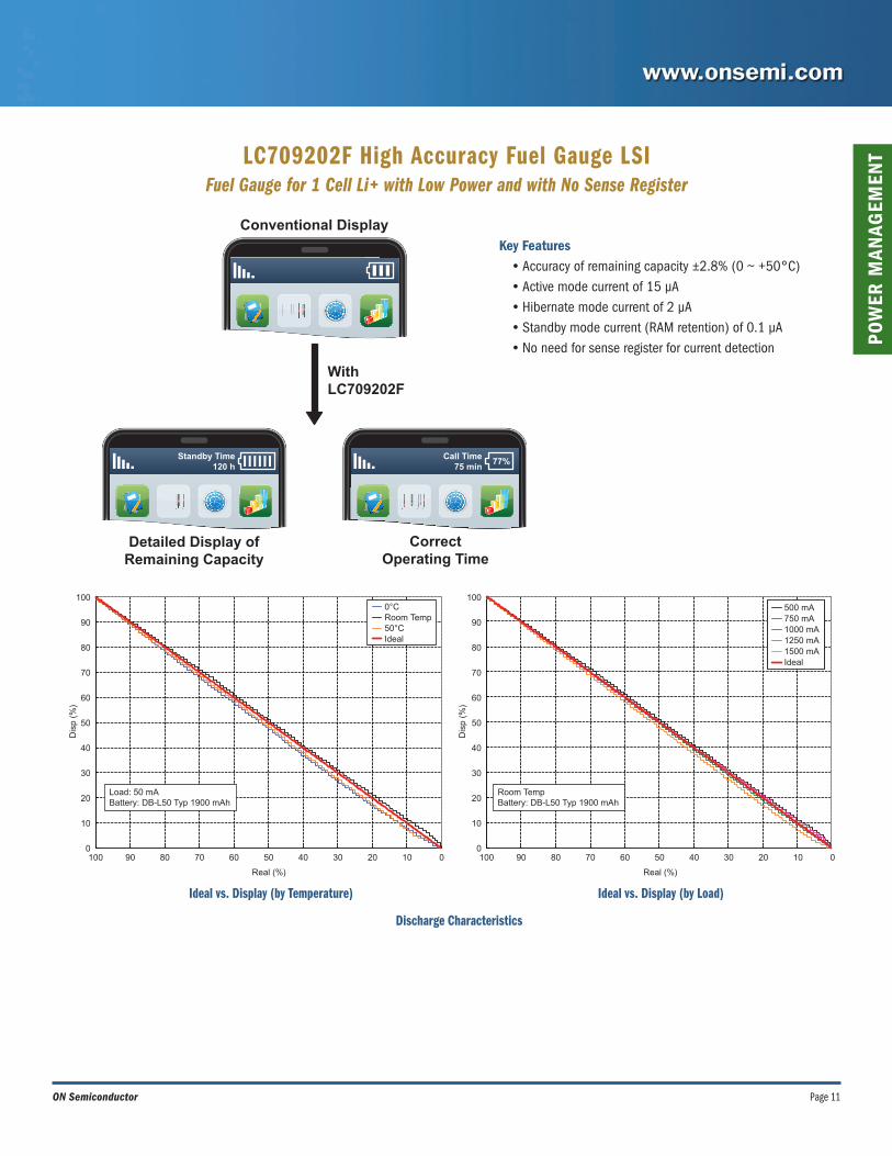
TLC709202F High Accuracy Fuel Gauge LSIFuel Gauge for 1 Cell Li+ with Low Power and with No Sense Register
Key Features• Accuracy of remaining capacity ±2.8% (0 ~ +50°C)• Active mode current of 15 µA• Hibernate mode current of 2 µA• Standby mode current (RAM retention) of 0.1 µA• No need for sense register for current detection
Conventional Display
Detailed Display ofRemaining Capacity
CorrectOperating Time
WithLC709202F
Standby Time120 h
Call Time75 min
77%
Ideal vs. Display (by Temperature) Ideal vs. Display (by Load)
Discharge Characteristics
100
100 90 80 70 60 50 40 30 20 10 0 100 90 80 70 60 50 40 30 20 10 0
90
80
70
60
50
40
30
20
10
0
100
90
80
70
60
50
40
30
20
10
0
Real (%)
Dis
p (%
)
Dis
p (%
)
Load: 50 mABattery: DB-L50 Typ 1900 mAh
Room TempBattery: DB-L50 Typ 1900 mAh
Real (%)
0°CRoom Temp50°CIdeal
500 mA750 mA1000 mA1250 mA1500 mAIdeal
Page 12 Portable Solutions
POW
ER M
ANAG
EMEN
T
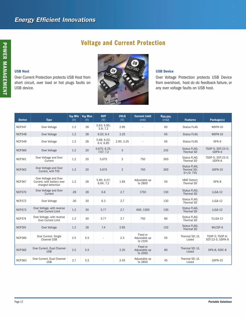
Voltage and Current Protection
USB Host
Over Current Protection protects USB Host from short circuit, over load or hot plugs faults on USB device.
USB Device
Over Voltage Protection protects USB Device from overshoot, host dc-dc feedback failure, or any over voltage faults on USB host.
Device TypeVIN Min
(V) VIN Max
(V)OVP(V)
UVLO(V)
Current Limit(mA)
RDS(ON) (mW) Features Package(s)
NCP347 Over Voltage 1.2 28 5.63; 5.85; 5.9; 7.2 2.95 - 65 Status FLAG WDFN-10
NCP348 Over Voltage 1.2 28 6.02; 6.4 3.25 - 65 Status FLAG WDFN-10
NCP349 Over Voltage 1.2 28 5.68; 6.02; 6.4; 6.85 2.95; 3.25 - 65 Status FLAG DFN-6
NCP360 Over Voltage 1.2 20 5.675; 6.25; 7.07; 7.2 3 - 210 Status FLAG;
Thermal SDTSOP-5; SOT-23-5;
UDFN-6
NCP361 Over Voltage and Over Current 1.2 20 5.675 3 750 300 Status FLAG;
Thermal SDTSOP-5; SOT-23-5;
UDFN-6
NCP362 Over Voltage and Over Current, with TVS 1.2 20 5.675 3 750 300
Status FLAG; Thermal SD; D+/D- TVS
UDFN-10
NCP367 Over Voltage and Over
Current, with battery over charged detection
1.2 28 5.85; 6.07; 6.84; 7.2 1.85 Adjustable up
to 2800 50 VBAT Detect; Thermal SD DFN-8
NCP370 Over Voltage and Over Current -28 28 6.6 2.7 1750 130 Status FLAG;
Thermal SD LLGA-12
NCP372 Over Voltage -30 30 6.3 2.7 - 130 Status FLAG; Thermal SD LLGA-12
NCP373 Over Voltage, with reverse Over Current Limit 1.2 30 5.77 2.7 400; 1300 130 Status FLAG;
Thermal SD LLGA-12
NCP374 Over Voltage, with reverse Over Current Limit 1.2 30 5.77 2.7 750 80 Status FLAG;
Thermal SD TLLGA-12
NCP391 Over Voltage 1.2 28 7.4 2.95 - 120 Status FLAG; Thermal SD WLCSP-6
NCP380 Over Current, Single Channel USB 2.5 5.5 - 2.3
Fixed or Adjustable up
to 2100 55 Thermal SD; UL
ListedTSOP-5; TSOP-6;
SOT-23-5; UDFN-6
NCP382 Over Current, Dual Channel USB 2.5 5.5 - 2.35
Fixed or Adjustable up
to 200080 Thermal SD; UL
Listed DFN-8; SOIC-8
NCP383 Over Current, Dual Channel USB 2.7 5.5 - 2.45 Adjustable up
to 2800 45 Thermal SD; UL Listed UDFN-10
Page 13ON Semiconductor
RF
CO
MPO
NEN
TS
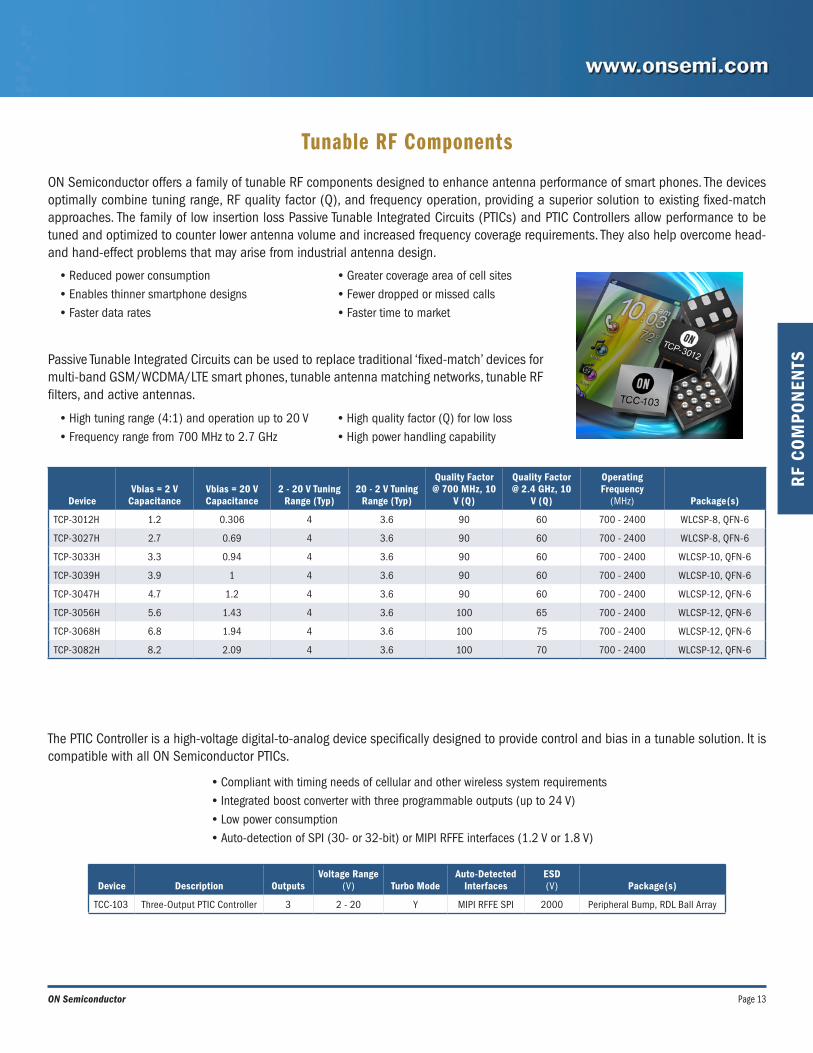
Tunable RF Components
ON Semiconductor offers a family of tunable RF components designed to enhance antenna performance of smart phones. The devices optimally combine tuning range, RF quality factor (Q), and frequency operation, providing a superior solution to existing fixed-match approaches. The family of low insertion loss Passive Tunable Integrated Circuits (PTICs) and PTIC Controllers allow performance to be tuned and optimized to counter lower antenna volume and increased frequency coverage requirements. They also help overcome head- and hand-effect problems that may arise from industrial antenna design.
Passive Tunable Integrated Circuits can be used to replace traditional ‘fixed-match’ devices for multi-band GSM/WCDMA/LTE smart phones, tunable antenna matching networks, tunable RF filters, and active antennas.
The PTIC Controller is a high-voltage digital-to-analog device specifically designed to provide control and bias in a tunable solution. It is compatible with all ON Semiconductor PTICs.
DeviceVbias = 2 V
CapacitanceVbias = 20 VCapacitance
2 - 20 V Tuning Range (Typ)
20 - 2 V Tuning Range (Typ)
Quality Factor @ 700 MHz, 10
V (Q)
Quality Factor @ 2.4 GHz, 10
V (Q)
OperatingFrequency
(MHz) Package(s)
TCP-3012H 1.2 0.306 4 3.6 90 60 700 - 2400 WLCSP-8, QFN-6
TCP-3027H 2.7 0.69 4 3.6 90 60 700 - 2400 WLCSP-8, QFN-6
TCP-3033H 3.3 0.94 4 3.6 90 60 700 - 2400 WLCSP-10, QFN-6
TCP-3039H 3.9 1 4 3.6 90 60 700 - 2400 WLCSP-10, QFN-6
TCP-3047H 4.7 1.2 4 3.6 90 60 700 - 2400 WLCSP-12, QFN-6
TCP-3056H 5.6 1.43 4 3.6 100 65 700 - 2400 WLCSP-12, QFN-6
TCP-3068H 6.8 1.94 4 3.6 100 75 700 - 2400 WLCSP-12, QFN-6
TCP-3082H 8.2 2.09 4 3.6 100 70 700 - 2400 WLCSP-12, QFN-6
Device Description OutputsVoltage Range
(V) Turbo ModeAuto-Detected
InterfacesESD(V) Package(s)
TCC-103 Three-Output PTIC Controller 3 2 - 20 Y MIPI RFFE SPI 2000 Peripheral Bump, RDL Ball Array
• Reduced power consumption• Enables thinner smartphone designs• Faster data rates
• Greater coverage area of cell sites • Fewer dropped or missed calls• Faster time to market
• High tuning range (4:1) and operation up to 20 V• Frequency range from 700 MHz to 2.7 GHz
• High quality factor (Q) for low loss• High power handling capability
• Compliant with timing needs of cellular and other wireless system requirements• Integrated boost converter with three programmable outputs (up to 24 V)• Low power consumption• Auto-detection of SPI (30- or 32-bit) or MIPI RFFE interfaces (1.2 V or 1.8 V)

Page 14 Portable Solutions
RF C
OM
PON
ENTS
RF Switches for WLAN
Key Features• Low insertion loss for higher transmitter efficiency and receive sensitivity• Strong ESD immunity for high reliability• Small PCB footprint, low profile
LNA
RX
PA
BPF
Antenna
SPDT
TX
LNA
RX W-LAN/BT
PA
BPF
Antenna
SP3T
TX W-LAN
TX BT
Device TypeVDD(V)
Frequency(GHz)
IL(dB)
ISO(dB)
Pin1dB(dBm) Package(s)
SPM3330* SPDT 32.5 0.37 28 32
XDFN-66.0 0.47 33 32
SPM3331* SP3T 32.5 0.45 28 30
XDFN-86.0 0.75 25 30
* Pending 3Q13.

Page 15ON Semiconductor
RF
CO
MPO
NEN
TS
Integrated Passive Devices ( IPD)• Combines multiple resistors, capacitors and inductors onto a film substrate; typical applications include RF baluns, filters, and
matching networks• Reduces PCB footprint and component height versus discrete implementations, while also improving performance (reduced parasitics)• Simplifies logistics, inventory managememt and pick-and-place assembly by elimination of multiple discrete passive SKUs• Based on 110 nm silicon process with high performance and tight process control
• Wafers manufactured on high precision equipment, designed for 110 nm transistor fabrication
• Very tight performance tolerances and low variation across wafers• ±4.3% tolerance 1K MIM caps• ±3.9% tolerance 2K MIM caps• < 1% variance between caps on common IPD
Integration of multiple R, L, and Cinto single IPD
Available Components
• MIM capacitors, 0.62 nF/mm2 , typical tolerance ±5%
• TiN resistors, 9 W/sq
• Copper inductors, minimum spacing 3 µm, minimum line width 5 µm, current handling >50 mA/µm, achieves Q-factors up to 45
Picked & Diced Wafer Edge
Inductor Within IPD (SEM Photo)
Sub-Micron Tolerances — Trace Spacing/Width Down to 3/5 mm
Page 16 Portable Solutions
DISPLAY
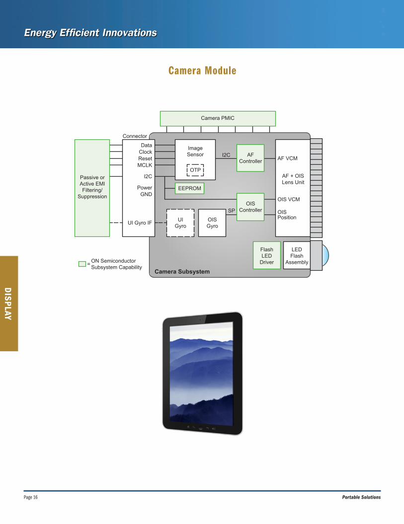
Camera Module
Data
OIS VCM
AF VCM
AF + OISLens Unit
OISPosition
ClockResetMCLK
I2C
SP
I2C
PowerGND
UI Gyro IF
ImageSensor
UIGyro
OISGyro
LEDFlash
Assembly
FlashLED
Driver
OISController
AFController
Camera PMIC
OTP
EEPROM
Passive orActive EMIFiltering/
Suppression
Connector
Camera Subsystem
ON SemiconductorSubsystem Capability
=
Page 17ON Semiconductor
DIS
PLAY
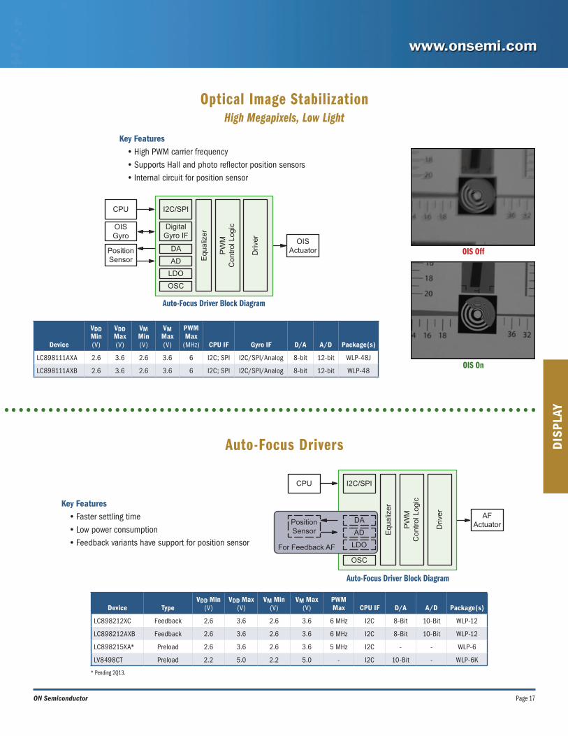
Optical Image StabilizationHigh Megapixels, Low Light
Auto-Focus Drivers
Key Features• High PWM carrier frequency• Supports Hall and photo reflector position sensors• Internal circuit for position sensor
Key Features• Faster settling time• Low power consumption• Feedback variants have support for position sensor
OIS Off
OIS On
Device TypeVDD Min
(V)VDD Max
(V)VM Min
(V)VM Max
(V)PWM Max CPU IF D/A A/D Package(s)
LC898212XC Feedback 2.6 3.6 2.6 3.6 6 MHz I2C 8-Bit 10-Bit WLP-12
LC898212AXB Feedback 2.6 3.6 2.6 3.6 6 MHz I2C 8-Bit 10-Bit WLP-12
LC898215XA* Preload 2.6 3.6 2.6 3.6 5 MHz I2C - - WLP-6
LV8498CT Preload 2.2 5.0 2.2 5.0 - I2C 10-Bit - WLP-6K
DigitalGyro IF
Equ
aliz
er
DA
I2C/SPICPU
PW
MC
ontr
ol L
ogic
Driv
erAD
LDO
OSC
OISGyro
PositionSensor
OISActuator
Auto-Focus Driver Block Diagram
Equ
aliz
er
DA
I2C/SPICPU
PW
MC
ontr
ol L
ogic
Driv
er
AD
LDO
OSC
PositionSensor
AFActuator
For Feedback AF
Auto-Focus Driver Block Diagram
Device
VDD Min(V)
VDD Max(V)
VM Min(V)
VM Max(V)
PWM Max
(MHz) CPU IF Gyro IF D/A A/D Package(s)
LC898111AXA 2.6 3.6 2.6 3.6 6 I2C; SPI I2C/SPI/Analog 8-bit 12-bit WLP-48J
LC898111AXB 2.6 3.6 2.6 3.6 6 I2C; SPI I2C/SPI/Analog 8-bit 12-bit WLP-48
* Pending 2Q13.
Page 18 Portable Solutions
DISPLAY
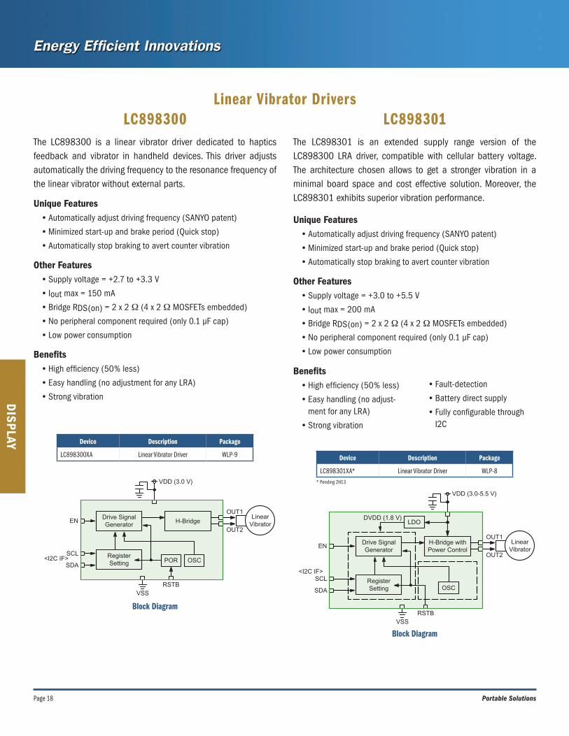
LC898300 LC898301
Device Description Package
LC898300XA Linear Vibrator Driver WLP-9 Device Description Package
LC898301XA* Linear Vibrator Driver WLP-8
Block Diagram
Block Diagram
Unique Features• Automatically adjust driving frequency (SANYO patent)
• Minimized start-up and brake period (Quick stop)
• Automatically stop braking to avert counter vibration
Other Features• Supply voltage = +2.7 to +3.3 V
• Iout max = 150 mA
• Bridge RDS(on) = 2 x 2 W (4 x 2 W MOSFETs embedded)
• No peripheral component required (only 0.1 µF cap)
• Low power consumption
Benefits• High efficiency (50% less)
• Easy handling (no adjustment for any LRA)
• Strong vibration
Unique Features• Automatically adjust driving frequency (SANYO patent)
• Minimized start-up and brake period (Quick stop)
• Automatically stop braking to avert counter vibration
Other Features• Supply voltage = +3.0 to +5.5 V
• Iout max = 200 mA
• Bridge RDS(on) = 2 x 2 W (4 x 2 W MOSFETs embedded)
• No peripheral component required (only 0.1 µF cap)
• Low power consumption
Benefits• High efficiency (50% less)
• Easy handling (no adjust-ment for any LRA)
• Strong vibration
• Fault-detection
• Battery direct supply
• Fully configurable through I2C
Linear Vibrator Drivers
The LC898300 is a linear vibrator driver dedicated to haptics feedback and vibrator in handheld devices. This driver adjusts automatically the driving frequency to the resonance frequency of the linear vibrator without external parts.
The LC898301 is an extended supply range version of the LC898300 LRA driver, compatible with cellular battery voltage. The architecture chosen allows to get a stronger vibration in a minimal board space and cost effective solution. Moreover, the LC898301 exhibits superior vibration performance.
H-Bridge withPower Control
Drive SignalGenerator
RegisterSetting OSC
LDO
SCL<I2C IF>
EN
DVDD (1.8 V)
VDD (3.0-5.5 V)
OUT1
OUT2
LinearVibrator
SDA
VSSRSTB
H-BridgeDrive SignalGenerator
RegisterSetting OSCPOR
SCL<I2C IF>
EN
VDD (3.0 V)
OUT1
OUT2
LinearVibrator
SDA
VSSRSTB
* Pending 2H13
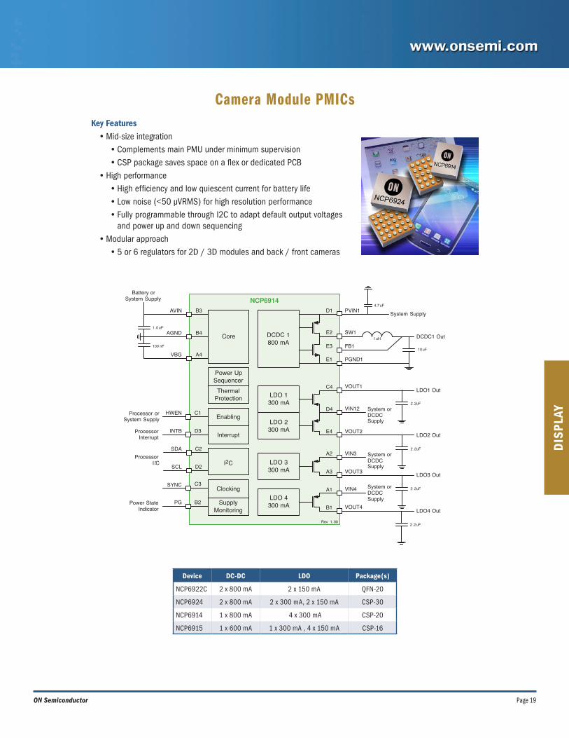
Page 19ON Semiconductor
DIS
PLAY
Camera Module PMICsKey Features• Mid-size integration
• Complements main PMU under minimum supervision• CSP package saves space on a flex or dedicated PCB
• High performance• High efficiency and low quiescent current for battery life• Low noise (<50 µVRMS) for high resolution performance• Fully programmable through I2C to adapt default output voltages
and power up and down sequencing• Modular approach
• 5 or 6 regulators for 2D / 3D modules and back / front cameras
Power StateIndicator
ProcessorInterrupt
ProcessorI C
Battery orSystem Supply
Processor orSystem Supply
System Supply
DCDC1 Out
System orDCDCSupply
System orDCDCSupply
LDO3 Out
LDO4 Out
4.7uF
10 uF
1uH
2 .2uF
2 .2uF
1 .0uF
LDO2 Out
2 .2uF
LDO1 Out
2 .2uF
System orDCDCSupply
100 nF
Core
NCP6914
LDO 3300 mA
LDO 4300 mA
LDO 1300 mA
LDO 2300 mA
AVIN
AGND
VIN3
VOUT3
VIN4
VOUT4
FB1
PVIN1
SW1
PGND1
VOUT1
VIN12
VOUT2Interrupt
Enabling
SupplyMonitoring
Power UpSequencer
ThermalProtection
SDA
SCL
SYNC
PG
HWEN
INTB
VBG
Rev 1.00
DCDC 1800 mA
B3
B4
A4
C1
D3
C2
D2
C3
B2B1
A1
A3
A2
E4
D4
C4
E1
E3
E2
D1
Clocking
I2C
Device DC-DC LDO Package(s)
NCP6922C 2 x 800 mA 2 x 150 mA QFN-20
NCP6924 2 x 800 mA 2 x 300 mA, 2 x 150 mA CSP-30
NCP6914 1 x 800 mA 4 x 300 mA CSP-20
NCP6915 1 x 600 mA 1 x 300 mA , 4 x 150 mA CSP-16
Page 20 Portable Solutions
DISPLAY
Ambient Light and Proximity Sensors
Key Features• Design flexibility/customization (i.e., EEPROM if desired for trimming)• 0.0125 lux detection with customizable filtering (i.e., Photopic Light Response)• Dark current and temperature compensation• Lowest power consumption per resolution bit• I2C Interface (including High Speed Mode) and no effect on bus during power down
SDA
1 k
Vin = 3.3 V
1 k
1 μFSCL
MCU LEDDrivers LEDs
SDA
SCL
VDDAmbient
LightSensor
VSS
hν
Device Description
Operating Voltage Range
(V)
Operating Temp Range
(°C)
Light Sensitivity Range
(Lux) Interface Package
NOA1212Analog Ambient Light Sensor with Dark Current
Compensation and high gain mode2.0 to 5.5 –40 to +85 ~0.01 to 100K Analog CUDFN-6
NOA1305*Digital Ambient Light Sensor with I2C Interface
and Dark Current Compensation2.0 to 3.6 –40 to +85 0.125 to 100K
I2C(Standard and Fast Modes)
CUDFN-6
NOA2301* Digital Proximity Sensor with Interrupt 2.3 to 3.6 –40 to +85 —I2C
(Standard, Fast and High-Speed Modes)CUDFN-6
NOA2302* Digital Slave Proximity Sensor with Interrupt 2.3 to 3.6 –40 to +85 —I2C
(Standard, Fast and High-Speed Modes)CUDFN-6
NOA3301Digital Proximity Sensor with Ambient Light Sensor
and Interrupt2.3 to 3.6 –40 to +85 ~0 to 64K
I2C(Standard, Fast and High-Speed Modes)
CUDFN-8
* Pending 2H13.
Page 21ON Semiconductor
LED
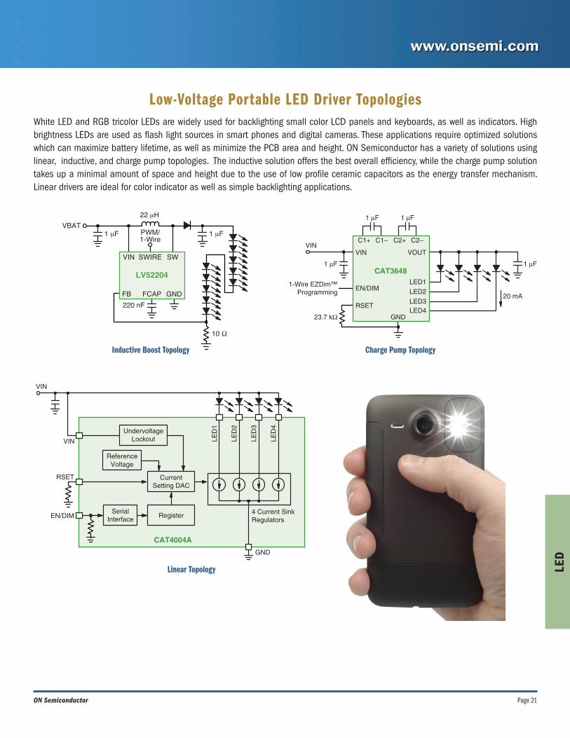
Low-Voltage Portable LED Driver TopologiesWhite LED and RGB tricolor LEDs are widely used for backlighting small color LCD panels and keyboards, as well as indicators. High brightness LEDs are used as flash light sources in smart phones and digital cameras. These applications require optimized solutions which can maximize battery lifetime, as well as minimize the PCB area and height. ON Semiconductor has a variety of solutions using linear, inductive, and charge pump topologies. The inductive solution offers the best overall efficiency, while the charge pump solution takes up a minimal amount of space and height due to the use of low profile ceramic capacitors as the energy transfer mechanism. Linear drivers are ideal for color indicator as well as simple backlighting applications.
20 mA
1 µF1 µF
23.7 kΩ
1-Wire EZDim™Programming
1 µF1 µF
LED1
VOUT
LED2
RSET
EN/DIM
VINVIN
LED3LED4
GND
CAT3648
C1+ C1– C2+ C2–
LED
1
4 Current SinkRegulators
CurrentSetting DAC
VIN
GND
VIN
RSET
EN/DIM
CAT4004A
LED
2
LED
3
LED
4
ReferenceVoltage
UndervoltageLockout
SerialInterface Register
Inductive Boost Topology Charge Pump Topology
Linear Topology
220 nF
1 μFVBAT
1 μF
10 Ω
LV52204
SW
GNDFCAP
22 μH
PWM/1-Wire
FB
VIN SWIRE

Page 22 Portable Solutions
LED
Charge Pump TopologyPatented Quad-Mode® adaptive fractional charge pumps take LED driver performance to a new level by offering a 10% efficiency improvement and up to 65% smaller packaging, without the need for an additional capacitor.
Quad-Mode LED drivers deliver the high efficiency levels normally associated with inductor-based LED drivers, while eliminating the associated high-profile inductors and unwanted EMI. Most charge pump LED drivers offer three modes of operation corresponding to the ratio of the output voltage to the input voltage: 1x, 1.5x and 2x. The Quad-Mode architecture adds a fourth mode of operation, 1.33x, without the need for the additional capacitor required by all other four-mode charge pumps.
Features• 4 charge pump modes: 1x, 1.33x, 1.5x, 2x• 10% higher efficiency versus 3-mode charge pumps• No additional capacitors• No inductor
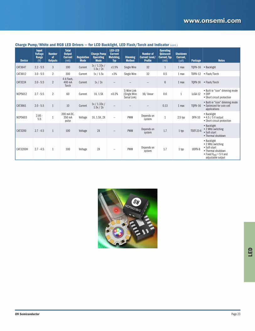
Charge Pump/White and RGB LED Drivers — for LCD Backlight, LED Flash/Torch and Indicator
Device
Input Voltage Range
(V)
Number of
Outputs
TotalOutput Current
(mA)Regulation
Mode
Charge Pump Operating
Mode
LED-LED Current
Matching, Typ
Dimming Method
Number of Current Level/
Profile
Operating Quiescent
Current, Typ(mA)
Shutdown Current
(mA) Package Notes
NCP1840 3.0 - 5.5 8 240 Current 1x / 1.33x / 1.5x / 2x ±2% I2C 32/ log 2.3 0.12 QFN-20
•Indicator application •Individual PWM programma- bility per channel; 64 different PWM duty cycle settings•Individual current level programmability (32 levels) per channel
CAT3606 2.7 - 5.5 6 180 Current 1x / 1.5x ±1.5% PWM Depends on System 1 1 max TQFN–16 •Backlight
CAT3616 2.7 - 5.5 6 186 Current 1x / 1.5x ±3% Single Wire 32 0.5 1 max TQFN–16 •Backlight
CAT3626 2.7 - 5.5 6 192 Current 1x / 1.5x ±3% I2C Depends on System 0.5 1 max TQFN–16 •Backlight
CAT3636 2.2 - 5.5 6 192 Current 1x / 1.33x / 1.5x / 2x ±1% Single Wire 32 0.5 1 max TQFN–16 •Backlight
CAT3637 2.2 - 5.5 6 192 Current 1x / 1.33x / 1.5x / 2x ±1% Single Wire 16 0.5 1 max TQFN–16 •Backlight
CAT3649 2.4 - 5.5 6 150 Current 1x / 1.33x / 1.5x / 2x ±1.5% Single Wire
& PWM 32 1.4 1 max TQFN–16 •Backlight
CAT3604A 2.7 - 5.5 4 120 Current 1x / 1.5x ±3% PWM Depends on System 0.3 0.05 typ TQFN–16 •Backlight
CAT3604V 2.7 - 5.5 4 120 Current 1x / 1.33x / 1.5x / 2x ±1.5% PWM Depends on
System 1 1 max TQFN–16 •Backlight
CAT3614 2.7 - 5.5 4 124 Current 1x / 1.5x ±3% Single Wire 32 0.5 1 max TDFN–12 •Backlight
CAT3644 2.2 - 5.5 4 100 Current 1x / 1.33x / 1.5x / 2x ±1.5% Single Wire 6 1 1 max TQFN–16 •Backlight
CAT3648 2.2 - 5.5 4 100 Current 1x / 1.33x / 1.5x / 2x ±1.5% Single Wire 32 1 1 max TQFN–16 •Backlight
NCP5623B/C 2.7 - 5.5 3(Independent) 90 Current 1X, 2X ±0.5% I2C 32/ quasi-log 0.35 0.8 typ LLGA-12
• RGB illumination •Backlight •Built-in “gradual illumination” •B & C versions have different I2C addresses
CAT3643 2.2 - 5.5 3 90 Current 1x / 1.33x / 1.5x / 2x ±1.5% Single Wire 6 1 1 max TDFN-12,
TQFN-16 •Backlight
Page 23ON Semiconductor
LED
Charge Pump/White and RGB LED Drivers — for LCD Backlight, LED Flash/Torch and Indicator (cont.)
Device
Input Voltage Range
(V)
Number of
Outputs
TotalOutput Current
(mA)Regulation
Mode
Charge Pump Operating
Mode
LED-LED Current
Matching, Typ
Dimming Method
Number of Current Level/
Profile
Operating Quiescent
Current, Typ(mA)
Shutdown Current,
(mA) Package Notes
CAT3647 2.2 - 5.5 3 100 Current 1x / 1.33x / 1.5x / 2x ±1.5% Single Wire 32 1 1 max TQFN–16 •Backlight
CAT3612 3.0 - 5.5 2 300 Current 1x / 1.5x ±3% Single Wire 32 0.5 1 max TDFN–12 •Flash/Torch
CAT3224 2.0 - 5.5 24 A Flash, 400 mA Torch
Current 1x / 2x — — — 6 1 max TQFN-16 •Flash/Torch
NCP5612 2.7 - 5.5 2 60 Current 1X, 1.5X ±0.2%S-Wire Link (Single Wire Serial Link)
16/ linear 0.6 1 LLGA-12•Built-in “icon” dimming mode •OVP•Short circuit protection
CAT3661 2.0 - 5.5 1 10 Current 1x / 1.33x / 1.5x / 2x — — — 0.13 1 max TQFN–16
•Built-in “icon” dimming mode •Optimized for coin cell applications
NCP5603 2.85 - 5.5 1
200 mA DC, 350 mA pulse
Voltage 1X, 1.5X, 2X — PWM Depends on system 1 2.5 typ DFN-10
•Backlight•4.5 / 5 V output•Short circuit protection
CAT3200 2.7 - 4.5 1 100 Voltage 2X — PWM Depends on system 1.7 1 typ TSOT-23-6
•Backlight•2 MHz switching•Soft-start•Thermal shutdown
CAT3200H 2.7 - 4.5 1 100 Voltage 2X — PWM Depends on system 1.7 1 typ UDFN-8
•Backlight•2 MHz switching•Soft-start•Thermal shutdown•Fixed Vout = 5 V and adjustable output
Page 24 Portable Solutions
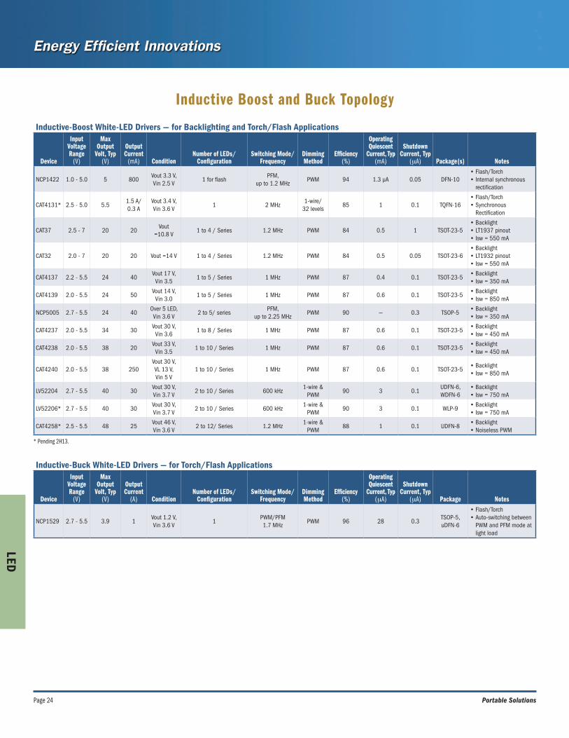
LED
Inductive Boost and Buck Topology
Inductive-Boost White-LED Drivers — for Backlighting and Torch/Flash Applications
Device
Input Voltage Range
(V)
Max Output
Volt, Typ (V)
Output Current
(mA) ConditionNumber of LEDs/
ConfigurationSwitching Mode/
FrequencyDimming Method
Efficiency (%)
Operating Quiescent
Current, Typ (mA)
Shutdown Current, Typ
(mA) Package(s) Notes
NCP1422 1.0 - 5.0 5 800Vout 3.3 V, Vin 2.5 V
1 for flashPFM,
up to 1.2 MHzPWM 94 1.3 µA 0.05 DFN-10
• Flash/Torch• Internal synchronous
rectification
CAT4131* 2.5 - 5.0 5.51.5 A/0.3 A
Vout 3.4 V,Vin 3.6 V
1 2 MHz1-wire/
32 levels85 1 0.1 TQFN-16
• Flash/Torch• Synchronous
Rectification
CAT37 2.5 - 7 20 20Vout
=10.8 V 1 to 4 / Series 1.2 MHz PWM 84 0.5 1 TSOT-23-5
• Backlight• LT1937 pinout• Isw = 550 mA
CAT32 2.0 - 7 20 20 Vout =14 V 1 to 4 / Series 1.2 MHz PWM 84 0.5 0.05 TSOT-23-6• Backlight• LT1932 pinout• Isw = 550 mA
CAT4137 2.2 - 5.5 24 40Vout 17 V, Vin 3.5
1 to 5 / Series 1 MHz PWM 87 0.4 0.1 TSOT-23-5• Backlight• Isw = 350 mA
CAT4139 2.0 - 5.5 24 50Vout 14 V, Vin 3.0
1 to 5 / Series 1 MHz PWM 87 0.6 0.1 TSOT-23-5• Backlight• Isw = 850 mA
NCP5005 2.7 - 5.5 24 40Over 5 LED, Vin 3.6 V
2 to 5/ seriesPFM,
up to 2.25 MHzPWM 90 — 0.3 TSOP-5
• Backlight• Isw = 350 mA
CAT4237 2.0 - 5.5 34 30Vout 30 V, Vin 3.6
1 to 8 / Series 1 MHz PWM 87 0.6 0.1 TSOT-23-5• Backlight• Isw = 450 mA
CAT4238 2.0 - 5.5 38 20Vout 33 V, Vin 3.5
1 to 10 / Series 1 MHz PWM 87 0.6 0.1 TSOT-23-5• Backlight• Isw = 450 mA
CAT4240 2.0 - 5.5 38 250Vout 30 V, VL 13 V, Vin 5 V
1 to 10 / Series 1 MHz PWM 87 0.6 0.1 TSOT-23-5• Backlight• Isw = 850 mA
LV52204 2.7 - 5.5 40 30Vout 30 V,Vin 3.7 V
2 to 10 / Series 600 kHz1-wire &
PWM90 3 0.1
UDFN-6, WDFN-6
• Backlight• Isw = 750 mA
LV52206* 2.7 - 5.5 40 30Vout 30 V,Vin 3.7 V
2 to 10 / Series 600 kHz1-wire &
PWM90 3 0.1 WLP-9
• Backlight• Isw = 750 mA
CAT4258* 2.5 - 5.5 48 25Vout 46 V,Vin 3.6 V
2 to 12/ Series 1.2 MHz1-wire &
PWM88 1 0.1 UDFN-8
• Backlight• Noiseless PWM
Inductive-Buck White-LED Drivers — for Torch/Flash Applications
Device
Input Voltage Range
(V)
Max Output
Volt, Typ (V)
Output Current
(A) ConditionNumber of LEDs/
ConfigurationSwitching Mode/
FrequencyDimming Method
Efficiency (%)
Operating Quiescent
Current, Typ (mA)
Shutdown Current, Typ
(mA) Package Notes
NCP1529 2.7 - 5.5 3.9 1Vout 1.2 V,Vin 3.6 V
1PWM/PFM1.7 MHz
PWM 96 28 0.3TSOP-5, uDFN-6
• Flash/Torch• Auto-switching between
PWM and PFM mode at light load
* Pending 2H13.

Page 25ON Semiconductor
LED
Linear Topology
Linear White-LED Drivers for LCD Backlight
Device No of Channels
Current Available Packages
Fixed(25 mA)
Adjustable(2 to 40 mA) SCL70-6 TSOT23-6 UDFN-8
CAT4002A 2 4 4 4
CAT4003B 3 4 4 4
CAT4004A 4 4 4
CAT4004B 4 4 4
Key Features• Dimming via 1-wire EZDim interface with
32 levels of dimming control• 25 mA fixed current (B versions) or
adjustable current (A versions)• Zero current shutdown (< 1 mA)• No switching supply noise• Tightly matched current LED sinks• Ultra-low headroom current sink• Dropout voltage of 75 mV at 20 mA• Low profile micro packaging
Applications• Mobile handsets• Still and video cameras• Portable gaming• Portable medical devices
32-Step EZDim Control
CIN1 μF
VIN2.4 to 5.5 V
1-WireProgramming
32 Steps
CAT4003B
LED1 LED2 LED3
GNDEN/DIM
VIN
Page 26 Portable Solutions
LED
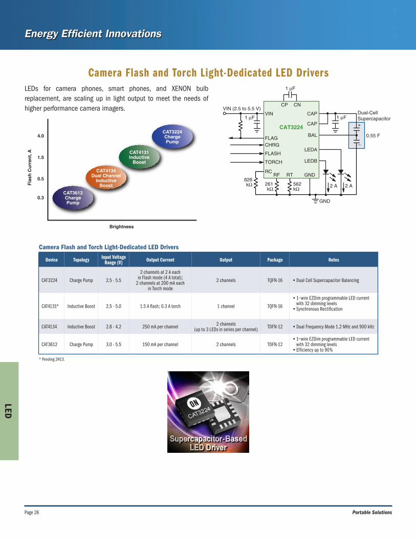
Camera Flash and Torch Light-Dedicated LED DriversLEDs for camera phones, smart phones, and XENON bulb replacement, are scaling up in light output to meet the needs of higher performance camera imagers.
CAT3612ChargePump
CAT4134Dual Channel
InductiveBoost
CAT4131Inductive
Boost
CAT3224ChargePump
Brightness
Flas
h C
urre
nt, A
0.5
0.3
1.5
4.0
Dual-CellSupercapacitor
2 A
0.55 F
1 µF1 µF
826kΩ 261
kΩ562kΩ
1 µF
2 A
LEDA
CAP
LEDB
CAP
BAL
RC
TORCH
FLASH
CHRGFLAG
VINVIN (2.5 to 5.5 V)
GND
GND
RF RT
CAT3224
CP CN
Camera Flash and Torch Light-Dedicated LED Drivers
Device Topology Input Voltage Range (V) Output Current Output Package Notes
CAT3224 Charge Pump 2.5 - 5.5
2 channels at 2 A each in Flash mode (4 A total);
2 channels at 200 mA each in Torch mode
2 channels TQFN-16 • Dual Cell Supercapacitor Balancing
CAT4131* Inductive Boost 2.5 - 5.0 1.5 A flash; 0.3 A torch 1 channel TQFN-16
• 1−wire EZDim programmable LED current with 32 dimming levels
• Synchronous Rectification
CAT4134 Inductive Boost 2.8 - 4.2 250 mA per channel 2 channels (up to 3 LEDs in series per channel) TDFN-12 • Dual Frequency Mode 1.2 MHz and 900 kHz
CAT3612 Charge Pump 3.0 - 5.5 150 mA per channel 2 channels TDFN-12• 1−wire EZDim programmable LED current
with 32 dimming levels• Efficiency up to 90%
* Pending 2H13.
Page 27ON Semiconductor
LED
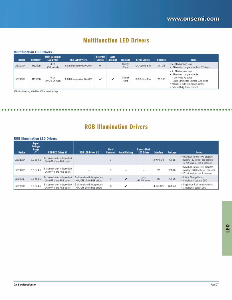
Multifunction LED Drivers
RGB Illumination Drivers
Multifunction LED Drivers
Device Function*Main Backlight
LED Driver RGB LED Driver 1External Control
Auto Blinking Topology Serial Control Package Notes
LV5207LP MB, RGB4-Ch
(3-Ch Avail)R,G,B Independent ON/OFF 4
ChargePump
I2C Control Bus VCT-24• 7 LED channels total• LED current programmable in 32 steps
LV5216CS MB, RGB6-Ch
(3/4/5-Ch Avail)R,G,B Independent ON/OFF 4 4
ChargePump
I2C Control Bus WLP-36
• 7 LED channels total• LED current programmable: – MB, RGB: 32 steps – Auto Luminance Control: 128 steps• Main LED auto luminance control• External brightness control
RGB Illumination LED Drivers
Device
Input Voltage Range
(V) RGB LED Driver #1 RGB LED Driver #2No of
Channels Auto BlinkingCamera Flash
LED Driver Interface Package Notes
LV5213LP 3.0 to 4.53-channels with independent
ON/OFF of the RGB colors— 3 — — 3-Wire SPI VCT-16
• Individual current level program-mability (32 levels) per channel
• 12 mA total for the 3 channels
LV5217LP 3.0 to 4.53-channels with independent
ON/OFF of the RGB colors— 3 — — I2C VCT-16
• Individual current level program-mability (128 levels) per channel
• 25 mA total for the 3 channels
LV5223GR 3.0 to 4.53-channels with independent
ON/OFF of the RGB colors3-channels with independent
ON/OFF of the RGB colors9 4
2-Ch (R2, G2 Common)
I2C VCT-28• Built-in Charge Pump• 3 additional outputs GPO
LV5226CS 3.0 to 4.53-channels with independent
ON/OFF of the RGB colors3-channels with independent
ON/OFF of the RGB colors6 4 — 4-wire SPI WLP-48
• 4 high-side P-channel switches• 1 additional output GPO
RGB=Illumination; MB=Main LCD screen backlight
Page 28 Portable Solutions
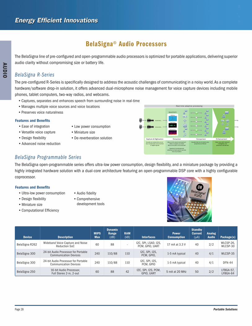
AUD
IO
The BelaSigna line of pre-configured and open-programmable audio processors is optimized for portable applications, delivering superior audio clarity without compromising size or battery life.
BelaSigna R-SeriesThe pre-configured R-Series is specifically designed to address the acoustic challenges of communicating in a noisy world. As a complete hardware/software drop-in solution, it offers advanced dual-microphone noise management for voice capture devices including mobile phones, tablet computers, two-way radios, and webcams.• Captures, separates and enhances speech from surrounding noise in real-time• Manages multiple voice sources and voice locations• Preserves voice naturalness
BelaSigna® Audio Processors
Features and Benefits• Ease of integration• Versatile voice capture• Design flexibility• Advanced noise reduction
• Low power consumption• Miniature size• De-reverberation solution
Features and Benefits• Ultra-low power consumption• Design flexibility• Miniature size• Computational Efficiency
• Audio fidelity• Comprehensive
development tools
BelaSigna Programmable SeriesThe BelaSigna open-programmable series offers ultra-low power consumption, design flexibility, and a miniature package by providing a highly integrated hardware solution with a dual-core architecture featuring an open-programmable DSP core with a highly configurable coprocessor.
Device DescriptionMIPS Max
Dynamic Range(dB)
RAM(kB) Interfaces
Power Consumption
Standby Current
(mA)Analog Audio Package(s)
BelaSigna R262 Wideband Voice Capture and Noise Reduction SoC 60 88 - I2C, SPI, LSAD, I2S,
PCM, GPIO, UART 17 mA at 3.3 V 40 2/2 WLCSP-26, WLCSP-30
BelaSigna 300 24-bit Audio Processor for Portable Communication Devices 240 110/88 110 I2C, SPI, I2S,
PCM, GPIO, 1-5 mA typical 40 4/1 WLCSP-35
BelaSigna 300 24-bit Audio Processor for Portable Communication Devices 240 110/88 110 I2C, SPI, I2S,
PCM, GPIO 1-5 mA typical 40 4/1 DFN-44
BelaSigna 250 16-bit Audio Processor, Full Stereo 2-in, 2-out 60 88 42 I2C, SPI, I2S, PCM,
GPIO, UART 5 mA at 20 MHz 50 2/2 LFBGA-57, LFBGA-64
010100001...
100111000...
Capture & DigitizationSounds are captured by one or two microphones and converted
to digital signals
ExtractionWhere is the sound coming from?
When is speech occuring?What is the pitch of the sounds?
Capable of simultaneously selecting multiple speech sources
from any location
ComparisonSounds that do not match voice
properties are filtered
EnhancementClear voice with improved
intelligibility andpreserved naturalness
SPATIAL
x
z
y
TEMPORAL
FREQUENCY
Real-time adaptive processing
SELECTIVITY
Page 29ON Semiconductor
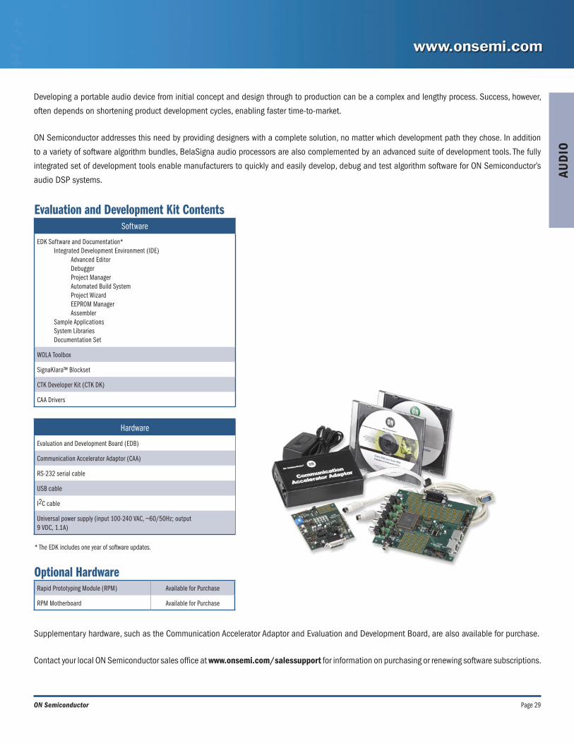
AUD
IO
Supplementary hardware, such as the Communication Accelerator Adaptor and Evaluation and Development Board, are also available for purchase.
Contact your local ON Semiconductor sales office at www.onsemi.com/salessupport for information on purchasing or renewing software subscriptions.
Developing a portable audio device from initial concept and design through to production can be a complex and lengthy process. Success, however,
often depends on shortening product development cycles, enabling faster time-to-market.
ON Semiconductor addresses this need by providing designers with a complete solution, no matter which development path they chose. In addition
to a variety of software algorithm bundles, BelaSigna audio processors are also complemented by an advanced suite of development tools. The fully
integrated set of development tools enable manufacturers to quickly and easily develop, debug and test algorithm software for ON Semiconductor’s
audio DSP systems.
Evaluation and Development Kit ContentsSoftware
EDK Software and Documentation* Integrated Development Environment (IDE) Advanced Editor Debugger Project Manager Automated Build System Project Wizard EEPROM Manager Assembler Sample Applications System Libraries Documentation Set
WOLA Toolbox
SignaKlara™ Blockset
CTK Developer Kit (CTK DK)
CAA Drivers
Optional HardwareRapid Prototyping Module (RPM) Available for Purchase
RPM Motherboard Available for Purchase
Hardware
Evaluation and Development Board (EDB)
Communication Accelerator Adaptor (CAA)
RS-232 serial cable
USB cable
I2C cable
Universal power supply (input 100-240 VAC, ~60/50Hz; output 9 VDC, 1.1A)
* The EDK includes one year of software updates.
Page 30 Portable Solutions
AUD
IO
To support the algorithm development process, ON Semiconductor offers an Evaluation and Development Kit (EDK) featuring an Integrated software Development Environment (IDE) for composing, compiling and debugging algorithm code. A Communication Accelerator Adaptor (CAA) connects the IDE running on a PC to a Rapid Prototyping Module (RPM) or Evaluation and Development Board (EDB)*. Using these components, developers can implement and immediately validate the performance of their proprietary algorithms, third-party algorithms, or other software integrated with BelaSigna bundles directly on BelaSigna hardware.
To evaluate audio processors and signal processing software, ON Semiconductor offers a solution that is easy to demonstrate, evaluate and design in. By evaluating pre-configured BelaSigna bundles developers can quickly evaluate the hardware and software, audio quality and processing power. They can then start the development process by selecting a suitable bundle, integrating custom functions with a bundle, or using software tools to develop their own signal processing algorithms to run on the BelaSigna hardware.
PC
IDE
CAA
RPM or EDB*
BelaSignaBundles
RPM
Algorithm DevelopmentSolution Evaluation
ON Semiconductor’s Integrated Development Environment is a fully integrated software development environment that enables developers to code, compile, debug and validate algorithms. Features include:
• Team based programming that greatly simplifies project management by allowing multiple developers to simultaneously work on the same design.
• Project wizard with templates based on sample algorithms, automatic no-maintenance project builder and system libraries to reduce development time.
• Integrated debugger providing full source code debugging and scriptable interface, customized expression watch, register, and memory views with changed value highlighting.
• Sample application source code provides complete sample algorithms plus samples of most basic application components.
• Advanced editor with content assist (command completion), syntax highlighting and integrated help enables context-sensitive, dynamic reference lookup.
• Full user and reference documentation set integrated with the IDE; dynamically searchable while editing.
• Interactive scripting console allowing developers to script activities within the IDE using a Python-like language, and to execute/test automated scripts that can interface with the chip and the development environment.
Integrated Development Environment (IDE)
Debug perspective showing (1) source code, (2) disassembly, (3) debug, (4) breakpoint, (5) expression, (6) register, (7) command console, (8) content assist, and (9) memory views.
Development perspective showing (1) advanced editor with (2) content assist, (3) dynamic help, (4) workspace navigator, (5) cheat sheets for common tasks, (6) outline view, (7) tasks, and (8) console views. Console shows build output and is a tabbed overlay with search, bookmark and error views.
1
2
3 45 6
78
1
6
2
4 3
5
7
8
9
+

Page 31ON Semiconductor
AUD
IO
ON Semiconductor enables form-factor hardware testing and prototyping with an RPM, optionally attached to a motherboard, that connects directly to a CAA. The RPM’s plug-in design enables developers to quickly transition from development in a simulation environment to testing a complete portable audio system. To facilitate development and testing even further, the RPM can be moved directly from the motherboard to a prototype for final hardware assessment.
Hardware Testing & Prototyping
PC
CTK DK
CAA
RPM or Proto
* EDB for BelaSigna 200 and 250 only.
To prepare portable audio products for the market, the CTK Run-time and CAA enable manufacturers to store firmware and data on an attached EEPROM, tune parameters on a unit-by-unit basis, configure the chip, and run final tests. By attaching a CAA directly to a Printed Circuit Board Assembly (PCBA), the CTK DK can be used to develop a customized software-controlled production flow to meet the specific needs of your production environment.
PCBA
Production & Final Testing
The Communication Accelerator Adaptor is a universal hardware adaptor that facilitates high-speed communication between host PCs (using USB 1.1 or 2.0) and ON Semiconductor development boards (EDB, RPM Motherboard). The CAA is reprogrammable and can also be used to transfer final software to products in a production or final test environment.
The Rapid Prototyping Module enables manufacturers to easily demonstrate and evaluate the audio performance and power consumption of ON Semiconductor audio processors in a real world environment. The small-footprint RPM is designed for easy attachment to existing portable audio devices while maintaining full portability. The RPM also facilitates fast and easy prototyping, and once concepts and possible configurations are tested and evaluated, the resulting integrated design will reduce risk and enable a faster time-to-market.
For added flexibility, a companion motherboard is also available that makes it easy to demonstrate and evaluate BelaSigna audio DSPs on their own, without the need for a product prototype. The motherboard also enables programming of the RPM. Full layout and schematic information for the RPM is provided with the board.
The Evaluation and Development Board enables the development, demonstration, testing and debugging of signal processing software. The EDB provides all peripherals needed for measurement and validation, including additional inputs and outputs for extra testing. By facilitating early validation of developed sound processing algorithm performance, the EDB helps to reduce overall development time.
Communication Accelerator Adapter (CAA)
Rapid Prototyping Module (RPM)
Evaluation and Development Board (EDB)
PASSED

Page 32 Portable Solutions
AUD
IO
The CTK Developer Kit is an easy-to-use universal software component library that facilitates communication with the DSP. It can be used in development, manufacturing, and testing environments. The CTK DK simplifies software development by supporting Python, COM (for Visual Basic, C/C++, C# and other .NET languages, Labview) and Java programming languages, eliminating the need for low-level protocol programming. The kit includes sample communication scripts and programs, searchable documentation, and full support for Python scripting. The CTK DK is available as an independent add-on
to the EDK.
* CTK Run-time is the communications driver for all software tools and scripts.
ON Semiconductor also offers BelaSigna bundles, ready-to-go algorithm solutions comprising a chip with an algorithm, that enable manufacturers to skip the algorithm development stage, and go straight from solution evaluation to hardware development. The bundles can be used to demonstrate, evaluate and/or design in BelaSigna hardware; additionally manufacturers can customize the algorithms to fit their unique requirements. A wide selection of bundles that address the most common audio processing needs are available; manufacturers can match their BelaSigna hardware with a corresponding list of algorithms to suit their portable audio needs.
ON Semiconductor is focused on providing a total
customer solution. If you need assistance with your
development efforts, we have a network of solution
partners to help get you to market fast.
Together with our solution partners, ON Semiconductor
creates an extended support network that enhances the
way customers can leverage our audio DSP technology.
CTK Developer Kit (CTK DK)
BelaSigna Bundles
Solution Partners
CTK Developer Kit integrated with IDE showing (1) telemetry sample application (running in the foreground), (2) dynamic help, including how to use CTK DK methods in common languages, (3) workspace navigator, (4) source code editor, and (5) console views. Console shows build output and is a tabbed overlay with task, error and bookmark views.
12
4
3
5
AUD
IOAU
DIO
Page 33ON Semiconductor
AUD
IO
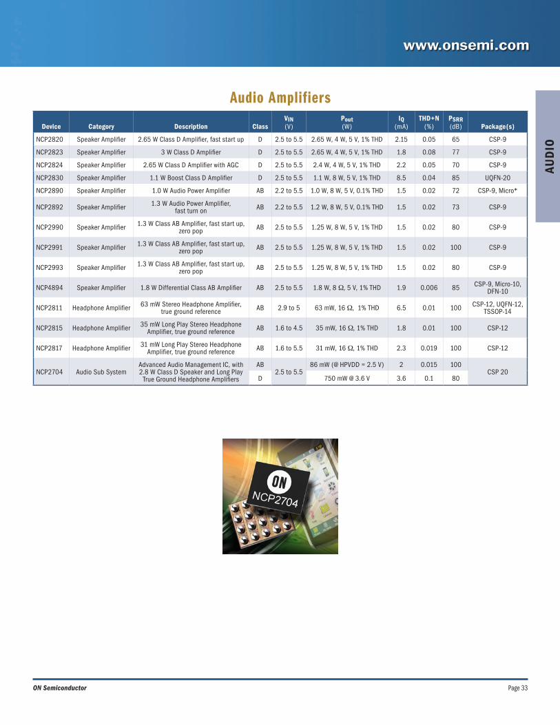
Audio Amplifiers
Device Category Description Class VIN(V)
Pout(W)
IQ(mA)
THD+N(%)
PSRR (dB) Package(s)
NCP2820 Speaker Amplifier 2.65 W Class D Amplifier, fast start up D 2.5 to 5.5 2.65 W, 4 W, 5 V, 1% THD 2.15 0.05 65 CSP-9
NCP2823 Speaker Amplifier 3 W Class D Amplifier D 2.5 to 5.5 2.65 W, 4 W, 5 V, 1% THD 1.8 0.08 77 CSP-9
NCP2824 Speaker Amplifier 2.65 W Class D Amplifier with AGC D 2.5 to 5.5 2.4 W, 4 W, 5 V, 1% THD 2.2 0.05 70 CSP-9
NCP2830 Speaker Amplifier 1.1 W Boost Class D Amplifier D 2.5 to 5.5 1.1 W, 8 W, 5 V, 1% THD 8.5 0.04 85 UQFN-20
NCP2890 Speaker Amplifier 1.0 W Audio Power Amplifier AB 2.2 to 5.5 1.0 W, 8 W, 5 V, 0.1% THD 1.5 0.02 72 CSP-9, Micro*
NCP2892 Speaker Amplifier 1.3 W Audio Power Amplifier, fast turn on AB 2.2 to 5.5 1.2 W, 8 W, 5 V, 0.1% THD 1.5 0.02 73 CSP-9
NCP2990 Speaker Amplifier 1.3 W Class AB Amplifier, fast start up, zero pop AB 2.5 to 5.5 1.25 W, 8 W, 5 V, 1% THD 1.5 0.02 80 CSP-9
NCP2991 Speaker Amplifier 1.3 W Class AB Amplifier, fast start up, zero pop AB 2.5 to 5.5 1.25 W, 8 W, 5 V, 1% THD 1.5 0.02 100 CSP-9
NCP2993 Speaker Amplifier 1.3 W Class AB Amplifier, fast start up, zero pop AB 2.5 to 5.5 1.25 W, 8 W, 5 V, 1% THD 1.5 0.02 80 CSP-9
NCP4894 Speaker Amplifier 1.8 W Differential Class AB Amplifier AB 2.5 to 5.5 1.8 W, 8 W, 5 V, 1% THD 1.9 0.006 85 CSP-9, Micro-10, DFN-10
NCP2811 Headphone Amplifier 63 mW Stereo Headphone Amplifier, true ground reference AB 2.9 to 5 63 mW, 16 W, 1% THD 6.5 0.01 100 CSP-12, UQFN-12,
TSSOP-14
NCP2815 Headphone Amplifier 35 mW Long Play Stereo Headphone Amplifier, true ground reference AB 1.6 to 4.5 35 mW, 16 W, 1% THD 1.8 0.01 100 CSP-12
NCP2817 Headphone Amplifier 31 mW Long Play Stereo Headphone Amplifier, true ground reference AB 1.6 to 5.5 31 mW, 16 W, 1% THD 2.3 0.019 100 CSP-12
NCP2704 Audio Sub System Advanced Audio Management IC, with 2.8 W Class D Speaker and Long Play
True Ground Headphone Amplifiers
AB2.5 to 5.5
86 mW (@ HPVDD = 2.5 V) 2 0.015 100CSP 20
D 750 mW @ 3.6 V 3.6 0.1 80
Page 34 Portable Solutions
INTER
FACE
Low Power Comparators
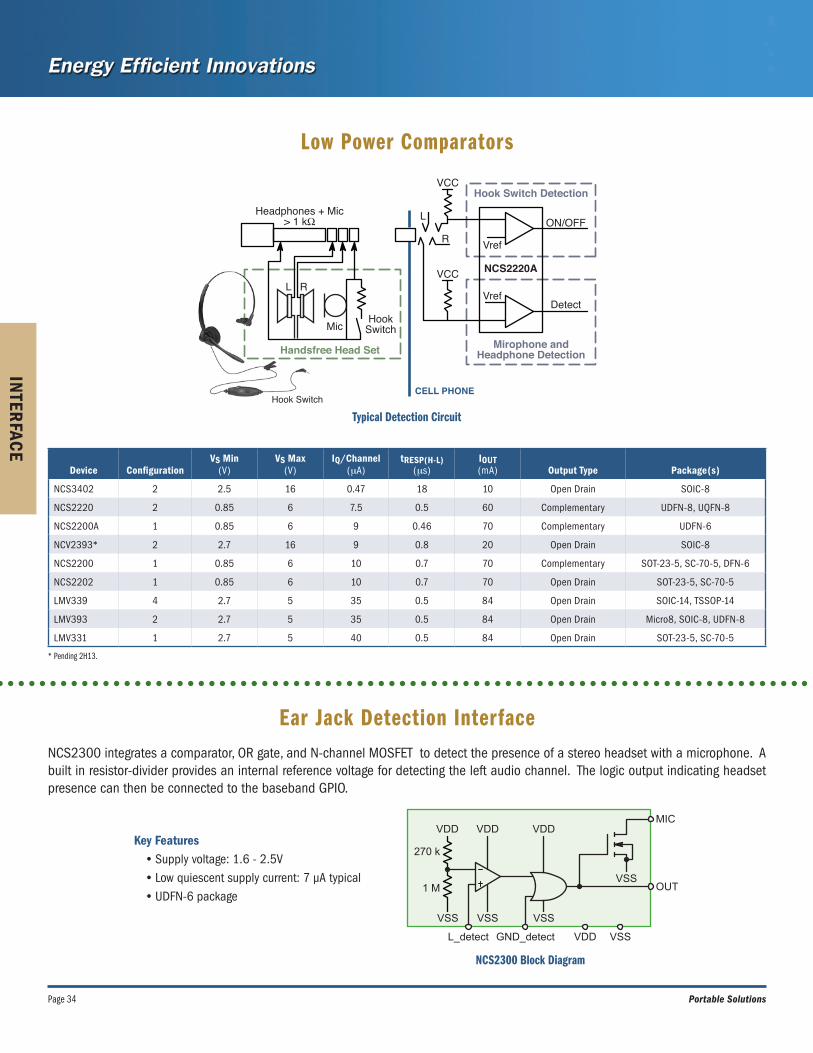
Ear Jack Detection Interface
Device ConfigurationVS Min
(V) VS Max
(V) IQ/Channel
(mA) tRESP(H-L)
(ms) IOUT (mA) Output Type Package(s)
NCS3402 2 2.5 16 0.47 18 10 Open Drain SOIC-8
NCS2220 2 0.85 6 7.5 0.5 60 Complementary UDFN-8, UQFN-8
NCS2200A 1 0.85 6 9 0.46 70 Complementary UDFN-6
NCV2393* 2 2.7 16 9 0.8 20 Open Drain SOIC-8
NCS2200 1 0.85 6 10 0.7 70 Complementary SOT-23-5, SC-70-5, DFN-6
NCS2202 1 0.85 6 10 0.7 70 Open Drain SOT-23-5, SC-70-5
LMV339 4 2.7 5 35 0.5 84 Open Drain SOIC-14, TSSOP-14
LMV393 2 2.7 5 35 0.5 84 Open Drain Micro8, SOIC-8, UDFN-8
LMV331 1 2.7 5 40 0.5 84 Open Drain SOT-23-5, SC-70-5
Handsfree Head Set
Hook Switch Detection
Mirophone andHeadphone Detection
NCS2220A
HookSwitch
Hook Switch
Headphones + Mic> 1 kΩ
Mic
R
R
VCC
Vref
L
L
VCC
Vref
ON/OFF
Detect
CELL PHONE
Typical Detection Circuit
NCS2300 Block Diagram
* Pending 2H13.
NCS2300 integrates a comparator, OR gate, and N-channel MOSFET to detect the presence of a stereo headset with a microphone. A built in resistor-divider provides an internal reference voltage for detecting the left audio channel. The logic output indicating headset presence can then be connected to the baseband GPIO.
Key Features• Supply voltage: 1.6 - 2.5V• Low quiescent supply current: 7 µA typical• UDFN-6 package
VSS
VSS
VSS
OUT
MIC
VDDGND_detectL_detect
VSS
VDDVDDVDD
VSS
270 k
1 M
Page 35ON Semiconductor
INTE
RFA
CE
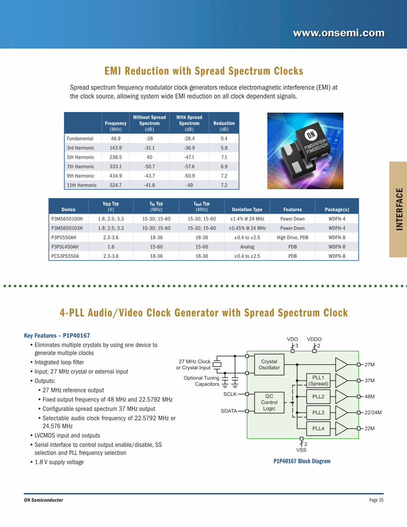
EMI Reduction with Spread Spectrum Clocks
4-PLL Audio/Video Clock Generator with Spread Spectrum Clock
Spread spectrum frequency modulator clock generators reduce electromagnetic interference (EMI) at the clock source, allowing system wide EMI reduction on all clock dependent signals.
Frequency (MHz)
Without Spread Spectrum
(dB)
With Spread Spectrum
(dB) Reduction
(dB)
Fundamental 46.9 -28 -28.4 0.4
3rd Harmonic 143.9 -31.1 -36.9 5.8
5th Harmonic 238.5 40 -47.1 7.1
7th Harmonic 333.1 -50.7 -57.6 6.9
9th Harmonic 434.9 -43.7 -50.9 7.2
11th Harmonic 524.7 -41.8 -49 7.2
DeviceVDD Typ
(V) fin Typ(MHz)
fout Typ(MHz) Deviation Type Features Package(s)
P3MS650100H 1.8; 2.5; 3.3 15-30; 15-60 15-30; 15-60 ±1.4% @ 24 MHz Power Down WDFN-4
P3MS650103H 1.8; 2.5; 3.3 15-30; 15-60 15-30; 15-60 ±0.45% @ 24 MHz Power Down WDFN-4
P3PS550AH 2.3-3.6 18-36 18-36 ±0.4 to ±2.5 High Drive, PDB WDFN-8
P3PSL450AH 1.8 15-60 15-60 Analog PDB WDFN-8
PCS3PS550A 2.3-3.6 18-36 18-36 ±0.4 to ±2.5 PDB WDFN-8
Key Features – P1P40167• Eliminates multiple crystals by using one device to
generate multiple clocks• Integrated loop filter • Input: 27 MHz crystal or external input • Outputs:
• 27 MHz reference output • Fixed output frequency of 48 MHz and 22.5792 MHz• Configurable spread spectrum 37 MHz output • Selectable audio clock frequency of 22.5792 MHz or
24.576 MHz• LVCMOS input and outputs• Serial interface to control output enable/disable, SS
selection and PLL frequency selection• 1.8 V supply voltage
CrystalOscillator
PLL1(Spread)
I2CControlLogic
SCLK
27M
VDO3
37M
48M
22/24M
22M
Optional TuningCapacitors
27 MHz Clockor Crystal Input
SDATA
PLL2
PLL3
PLL4
VDDO2
VSS2
P1P40167 Block Diagram
Page 36 Portable Solutions
INTER
FACE
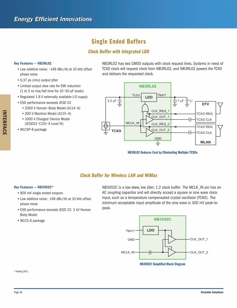
Single Ended BuffersClock Buffer with Integrated LDO
Clock Buffer for Wireless LAN and WiMax
Key Features — NB3RL02
• Low additive noise: −149 dBc/Hz at 10 kHz offset phase noise
• 0.37 ps (rms) output jitter
• Limited output slew rate for EMI reduction (1 to 5 ns rise/fall time for 10−50 pF loads)
• Regulated 1.8 V externally available I/O supply
• ESD performance exceeds JESD 22• 2000 V Human−Body Model (A114−A)• 200 V Machine Model (A115−A)• 1000 V Charged−Device Model
(JESD22−C101−A Level III)
• WLCSP-8 package
Key Features — NB3V02C*
• 800 mV single ended outputs
• Low additive noise: -149 dBc/Hz at 10 kHz offset phase noise
• ESD performance exceeds JESD 22: 2 kV Human Body Model
• WLCS-6 package
NB3RL02 has two CMOS outputs with clock request lines. Systems in need of TCXO clock will request clock from NB3RL02, and NB3RL02 powers the TCXO and delivers the requested clock.
NB3V02C is a low-skew, low jitter, 1:2 clock buffer. The MCLK_IN pin has an AC coupling capacitor and will directly accept a square or sine wave clock input, such as a temperature compensated crystal oscillator (TCXO). The minimum acceptable input amplitude of the sine wave is 300 mV peak-to-peak.
MCLK_IN
TCXO
CLK_REQ_1
VBATTVLDOLDO
GND
Li1 μF2.2 μF
CLK_OUT_1TCXO REQ
DTV
TCXO CLK
CLK_REQ_2
CLK_OUT_2TCXO REQ
WLAN
TCXO CLK
NB3RL02
NB3RL02 Reduces Cost by Eliminating Multiple TCXOs
NB3V02C Simplified Block Diagram
NB3V02C
MCLK_IN
VBATT LDO
GND CLK_OUT_1
CLK_OUT_2
* Pending 2H13.

Page 37ON Semiconductor
INTE
RFA
CE
LVDS Differential Buffer
2 :2 Buffer/Voltage Translator for Universal Flash Storage (UFS)
Key Features – NB3L14S• 1:4 LVDS clock buffer• 2.5 V operating voltage• Integrated input termination resistors• Maximum input clock frequency > 300 MHz • Low output-to-skew < 20 ps• 450 ps typical propagation delay• 250 ps typical rise/fall times• QFN-16 package
Key Features – NB3U23C*• Translates 1.8 V CMOS input to 1.2 V CMOS
output• Frequency >52 MHz maximum• Propagation delay <5 ns maximum• Output rise/fall times <2 ns • ESD Specifications exceed JESD22
• 2000 V Human-Body Model (A114-A) Operation
• 200 V Machine Model (A115-A)• 1000 V Charged-Device Model (C101)
• Noise floor density -145 dBc/Hz maximum• Phase noise -66 dBc(Hz) maximum, integrated
from 50 kHz – 10 MHz• Supply voltage 1.2 V ±5%• Standby current <15 µA• SC-70-6 package
NB3L14S Functional Diagram
INVTIN
Q1
Q1
50−50−
Q2
Q2
Q3
Q3
Q4
Q4
VCC
VCCM
IPI U
niPro
SM
MIP
I M-P
HY
SM
Application
UIC
UFSHostReg
UFS Host
DriverUFS HostController
1.2 V
0 - 1.2 V
0 - 1.2 V
RESET_n
REF CLK
DOUT_t
DOUT_c
DIN_t
DIN_c
0 - 1.8 V
0 - 1.8 VNB3U23C
UFS Device
* Pending 2H13.
Page 38 Portable Solutions
INTER
FACE
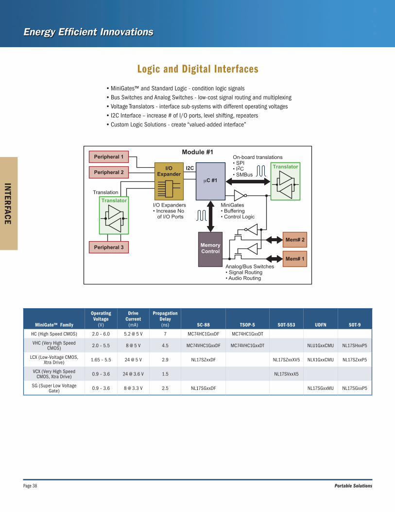
Logic and Digital Interfaces
• MiniGates™ and Standard Logic - condition logic signals• Bus Switches and Analog Switches - low-cost signal routing and multiplexing• Voltage Translators - interface sub-systems with different operating voltages• I2C Interface – increase # of I/O ports, level shifting, repeaters• Custom Logic Solutions - create “valued-added interface”
MiniGate™ Family
Operating Voltage
(V)
Drive Current
(mA)
Propagation Delay(ns) SC-88 TSOP-5 SOT-553 UDFN SOT-9
HC (High Speed CMOS) 2.0 – 6.0 5.2 @ 5 V 7 MC74HC1GxxDF MC74HC1GxxDT
VHC (Very High Speed CMOS) 2.0 – 5.5 8 @ 5 V 4.5 MC74VHC1GxxDF MC74VHC1GxxDT NLU1GxxCMU NL17SHxxP5
LCX (Low-Voltage CMOS, Xtra Drive) 1.65 – 5.5 24 @ 5 V 2.9 NL17SZxxDF NL17SZxxXV5 NLX1GxxCMU NL17SZxxP5
VCX (Very High Speed CMOS, Xtra Drive) 0.9 – 3.6 24 @ 3.6 V 1.5 NL17SVxxX5
SG (Super Low Voltage Gate) 0.9 – 3.6 8 @ 3.3 V 2.5 NL17SGxxDF NL17SGxxMU NL17SGxxP5
Translator
Mem# 2
Mem# 1
On-board translations• SPI• I2C• SMBus
Translation
MiniGates• Buffering• Control Logic
I/O Expanders• Increase No of I/O Ports
Analog/Bus Switches• Signal Routing• Audio Routing
Module #1
MemoryControl
Translator
μC #1
I/OExpander
Peripheral 1
Peripheral 2
Peripheral 3
I2C
Page 39ON Semiconductor
INTE
RFA
CE
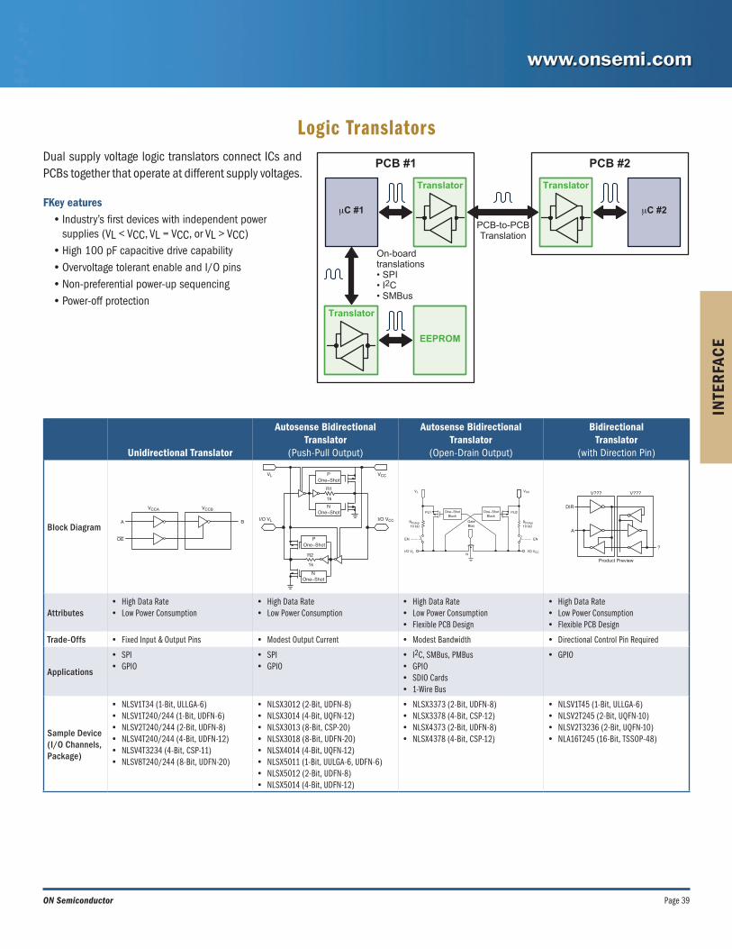
Logic TranslatorsDual supply voltage logic translators connect ICs and PCBs together that operate at different supply voltages.
FKey eatures• Industry’s first devices with independent power
supplies (VL < VCC, VL = VCC, or VL > VCC)• High 100 pF capacitive drive capability • Overvoltage tolerant enable and I/O pins • Non-preferential power-up sequencing • Power-off protection
Unidirectional Translator
Autosense BidirectionalTranslator
(Push-Pull Output)
Autosense BidirectionalTranslator
(Open-Drain Output)
BidirectionalTranslator
(with Direction Pin)
Block Diagram
VCCA VCCB
B
OE
A
POne−Shot
NOne−Shot
POne−Shot
NOne−Shot
VL
I/O VL I/O VCC
VCC
R1
R2
1k
1k
PU1
RPullup10 k
VL
I/O VL I/O VCC
VCC
One−ShotBlock
One−ShotBlock
PU2
GateBias
N
RPullup10 k
EN EN
?
A
DIR
V???
Product Preview
V???
Attributes• High Data Rate• Low Power Consumption
• High Data Rate• Low Power Consumption
• High Data Rate• Low Power Consumption• Flexible PCB Design
• High Data Rate• Low Power Consumption• Flexible PCB Design
Trade-Offs • Fixed Input & Output Pins • Modest Output Current • Modest Bandwidth • Directional Control Pin Required
Applications
• SPI• GPIO
• SPI• GPIO
• I2C, SMBus, PMBus• GPIO• SDIO Cards• 1-Wire Bus
• GPIO
Sample Device (I/O Channels, Package)
• NLSV1T34 (1-Bit, ULLGA-6)• NLSV1T240/244 (1-Bit, UDFN-6)• NLSV2T240/244 (2-Bit, UDFN-8)• NLSV4T240/244 (4-Bit, UDFN-12)• NLSV4T3234 (4-Bit, CSP-11)• NLSV8T240/244 (8-Bit, UDFN-20)
• NLSX3012 (2-Bit, UDFN-8)• NLSX3014 (4-Bit, UQFN-12)• NLSX3013 (8-Bit, CSP-20)• NLSX3018 (8-Bit, UDFN-20)• NLSX4014 (4-Bit, UQFN-12)• NLSX5011 (1-Bit, UULGA-6, UDFN-6)• NLSX5012 (2-Bit, UDFN-8)• NLSX5014 (4-Bit, UDFN-12)
• NLSX3373 (2-Bit, UDFN-8)• NLSX3378 (4-Bit, CSP-12)• NLSX4373 (2-Bit, UDFN-8)• NLSX4378 (4-Bit, CSP-12)
• NLSV1T45 (1-Bit, ULLGA-6)• NLSV2T245 (2-Bit, UQFN-10)• NLSV2T3236 (2-Bit, UQFN-10)• NLA16T245 (16-Bit, TSSOP-48)
Translator
EEPROM
Translator
Translator
On-boardtranslations• SPI• I2C• SMBus
PCB-to-PCBTranslation
PCB #1 PCB #2
μC #1 μC #2
Page 40 Portable Solutions
INTER
FACE
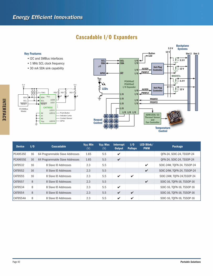
Cascadable I/O Expanders
Key Features• I2C and SMBus interfaces• 1 MHz SCL clock frequency• 30 mA SDA sink capability
Vext
Hot-PlugController
Hot-PlugController
ADM1030/33Thermal Sensor
andFan Controller
Slot 2 Slot 3
GPIO
PCA96xxEPCA95xxE
I/O Expander
I/O
I/O
I/O
I/O
SDAμC
SDASCL
PWRFLTAUXEN
SCL I/O
12 V
MOSFETs
3.3 V
PWRFLTAUXEN
I/OI/O
I/O
PRSNT2I/OPRSNT2I/O
I/O I/O I/O
I/O 12 V
3.3 V
12 V
3.3 V
I/O
ButtonLED
TemperatureControl
KeypadControl
LEDs
BackplaneSystems
INT
CAT9532I2C/SMBus
Master
VSS
A0
A1
A2
GPIO
Contact Sensor
Indicator Lamp
Push-Button
RS03 x 10kΩ RS1 RS11
5 V
LED11
LED1
LED0
VCC
LED12
LED15
SDA
5 V
SCL
SDA
SCL
RESETRESET
Device I/O CascadableVCC Min
(V)VCC Max
(V)Interrupt Output
I/O Pullups
LED Blink/ PWM
Package
PCA9535E 16 64 Programmable Slave Addresses 1.65 5.5 4 QFN-24, SOIC-24, TSSOP-24
PCA9655E 16 64 Programmable Slave Addresses 1.65 5.5 4 QFN-24, SOIC-24, TSSOP-24
CAT9532 16 8 Slave ID Addresses 2.3 5.5 4 SOIC-24W, TQFN-24, TSSOP-24
CAT9552 16 8 Slave ID Addresses 2.3 5.5 4 SOIC-24W, TQFN-24, TSSOP-24
CAT9555 16 8 Slave ID Addresses 2.3 5.5 4 4 SOIC-24W, TQFN-24,TSSOP-24
CAT9557 8 8 Slave ID Addresses 2.3 5.5 4 SOIC-16, TQFN-16, TSSOP-16
CAT9534 8 8 Slave ID Addresses 2.3 5.5 4 SOIC-16, TQFN-16, TSSOP-16
CAT9554 8 8 Slave ID Addresses 2.3 5.5 4 4 SOIC-16, TQFN-16, TSSOP-16
CAT9554A 8 8 Slave ID Addresses 2.3 5.5 4 4 SOIC-16, TQFN-16, TSSOP-16

Page 41ON Semiconductor
INTE
RFA
CE
Analog Switches
Small Signal MOSFETs
Device Data Type Configuration VCC Min
(V)VCC Max
(V)RON Max
(W) IIkg Max
(mA) C
(pF)BW
(MHz) Package(s)
NLAS7213 USB 2.0/UART DPST 1.65 4.5 10 1 5 1100 UQFN-8
NLAS4717 USB 1.1/UART Dual SPDT 1.8 5.5 4.5 1 110 40 Flip-Chip-10, Micro-10
NLAS4717EP USB 1.1/UART Dual SPDT 1.8 5.5 4.5 1 38 90 WQFN-10, Flip-Chip-10
NLAS7222A USB 2.0/UART DPDT 3 3.6 9 1 7 500 WQFN-10
NLAS7222B USB 2.0/UART DPDT 1.65 4.5 8 1 8 500 UQFN-10
NLAS7222C USB 2.0/UART DPDT 1.65 4.5 8 1 10 500 UQFN-10
NLAS7242 USB 2.0/UART DPDT 1.65 4.5 7.5 1 7.5 900 UQFN-10
NLAS8252 USB 1.1/UART DP3T 1.65 4.5 6 1 16 200 UQFN-12
NCN9252 USB 2.0/UART DP3T 1.65 4.5 6 1 16 525 UQFN-12
NLAS3899B SIM card Dual DPDT 1.65 4.3 4 1 20 280 WQFN-16, QFN-16
NS5S1153 USB 2.0/UART/Negative Audio DPDT -0.5 5 4.6 35 7 900 UQFN-10
NCN1154 USB 2.0/UART/Negative Audio DP3T -0.5 6 3 50 9 850 UQFN-12
NCN1188 USB 2.0/MHL 1.1/Negative Audio DP3T -0.5 6 - - - - UQFN-12
Device Polarity Configuration
V(BR)DSS Min(V)
VGS Max(V)
ID Max(A)
RDS(ON) Max @ VGS = 4.5 V
(W)
RDS(ON) Max @ VGS = 2.5 V
(W)
RDS(ON) Max @ VGS = 1.8 V
(W) Package(s)
NTNS3193NZ Single N-Channel 20 ±8 0.23 1.4 1.9 2.2 XLLGA-3
NTNS3A91PZ Single P-Channel -20 ±8 0.21 1.6 2.4 3.3 XLLGA-3
NTNS3164NZ Single N-Channel 20 ±8 0.22 0.7 1 2 SOT-883
NTNS3A65PZ Single P-Channel -20 ±8 0.23 1.3 2 3.4 SOT-883
NTNUS3171PZ Single P-Channel -20 ±8 0.15 3.5 4 5.5 SOT-1123
NTK3139P Single P-Channel -20 ±6 0.78 0.48 0.67 0.95 SOT-723
NTK3134N Single N-Channel 20 ±6 0.89 0.35 0.45 0.65 SOT-723
NTK3043N Single N-Channel 20 ±10 0.26 3.4 4.5 10 SOT-723
SCH1342* Single P-Channel -12 ±10 -4.5 0.041 0.053 0.073 SOT-563
NTZS3151P Single P-Channel -20 ±8 0.9 0.142 0.2 0.24 SOT-563
NTUD3170NZ Dual N-Channel 20 ±8 0.22 1.5 2 3 SOT-963
NTZD3152P Dual P-Channel -20 ±6 0.4 0.9 1.2 2 SOT-563
NTZD3154N Dual N-Channel 20 ±6 0.5 0.55 0.7 0.9 SOT-563
NTZD5110N Dual N-Channel 60 ±20 0.3 2.5 - - SOT-563
NTUD3169CZ ComplementaryN-Channel -20 ±8 0.22 1.5 2 3
SOT-963P-Channel 20 ±8 0.25 5 6 7
NTZD3155C ComplementaryN-Channel 20 ±6 0.54 0.55 0.7 0.9
SOT-563P-Channel -20 ±6 0.43 0.9 1.2 2
* Pending 2H13.
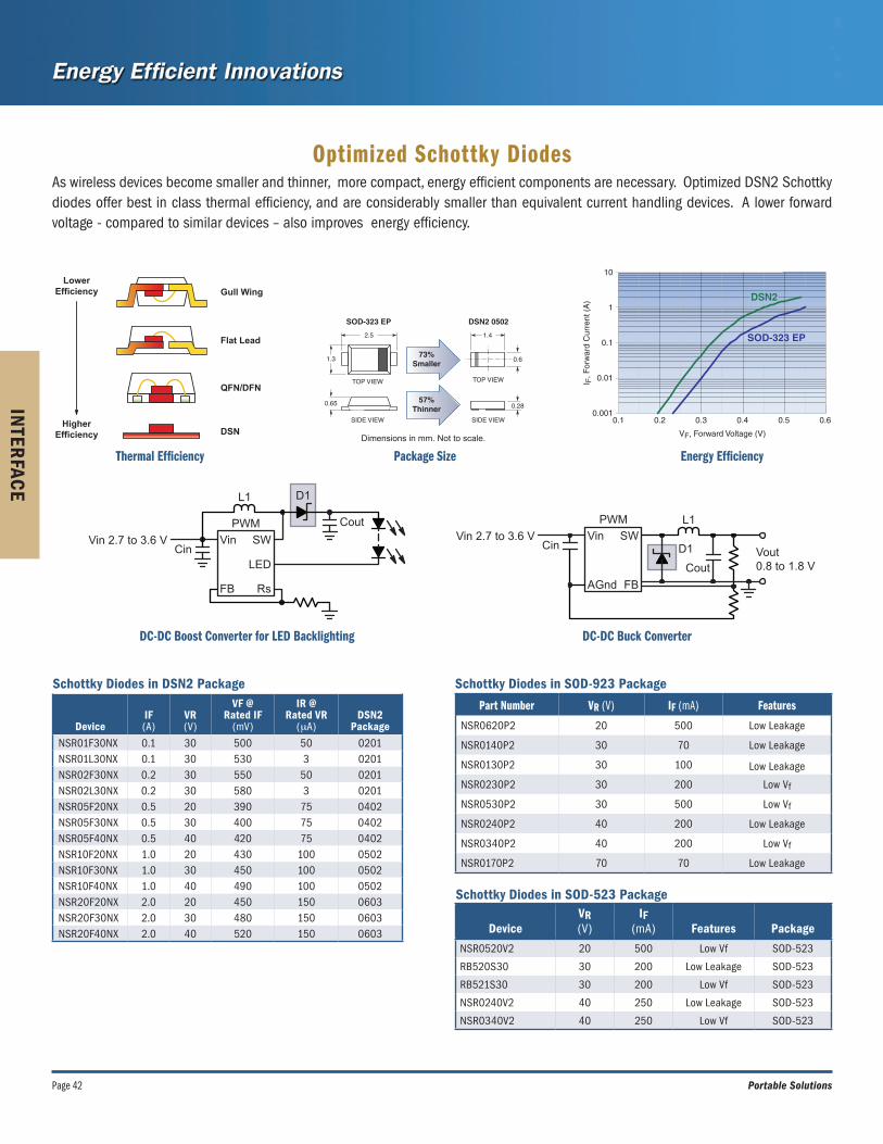
Page 42 Portable Solutions
INTER
FACE
Optimized Schottky Diodes
Schottky Diodes in DSN2 Package
DeviceIF (A)
VR (V)
VF @ Rated IF
(mV)
IR @ Rated VR
(mA)DSN2
PackageNSR01F30NX 0.1 30 500 50 0201NSR01L30NX 0.1 30 530 3 0201NSR02F30NX 0.2 30 550 50 0201NSR02L30NX 0.2 30 580 3 0201NSR05F20NX 0.5 20 390 75 0402NSR05F30NX 0.5 30 400 75 0402NSR05F40NX 0.5 40 420 75 0402NSR10F20NX 1.0 20 430 100 0502NSR10F30NX 1.0 30 450 100 0502NSR10F40NX 1.0 40 490 100 0502NSR20F20NX 2.0 20 450 150 0603NSR20F30NX 2.0 30 480 150 0603NSR20F40NX 2.0 40 520 150 0603
Schottky Diodes in SOD-923 Package
Part Number VR (V) IF (mA) Features
NSR0620P2 20 500 Low Leakage
NSR0140P2 30 70 Low Leakage
NSR0130P2 30 100 Low Leakage
NSR0230P2 30 200 Low Vf
NSR0530P2 30 500 Low Vf
NSR0240P2 40 200 Low Leakage
NSR0340P2 40 200 Low Vf
NSR0170P2 70 70 Low Leakage
Schottky Diodes in SOD-523 Package
DeviceVR (V)
IF (mA) Features Package
NSR0520V2 20 500 Low Vf SOD-523
RB520S30 30 200 Low Leakage SOD-523
RB521S30 30 200 Low Vf SOD-523
NSR0240V2 40 250 Low Leakage SOD-523
NSR0340V2 40 250 Low Vf SOD-523
As wireless devices become smaller and thinner, more compact, energy efficient components are necessary. Optimized DSN2 Schottky diodes offer best in class thermal efficiency, and are considerably smaller than equivalent current handling devices. A lower forward voltage - compared to similar devices – also improves energy efficiency.
1.4
0.6
0.280.65
1.3
2.5
TOP VIEWTOP VIEW
DSN2 0502SOD-323 EP
SIDE VIEWSIDE VIEW
73%Smaller
57%Thinner
Dimensions in mm. Not to scale.
0.1 0.2 0.3 0.4
VF, Forward Voltage (V)
I F, F
orw
ard
Cur
rent
(A
) DSN2
SOD-323 EP
0.5 0.60.001
0.01
0.1
1
10
Package SizeThermal Efficiency Energy Efficiency
Gull WingLower
Efficiency
HigherEfficiency
Flat Lead
QFN/DFN
DSN
DC-DC Boost Converter for LED Backlighting DC-DC Buck Converter
CinVin
FB
SW
PWM
L1 D1
Rs
LED
Vin 2.7 to 3.6 V
Cout
CinVin
AGnd
SW
PWM
Vout0.8 to 1.8 V
L1
D1
FB
Vin 2.7 to 3.6 V
Cout
Page 43ON Semiconductor
INTE
RFA
CE
Bipolar Transistors and Digital Transistors
Bipolar Transistors
ON Semiconductor offers a wide portfolio of general purpose Bipolar Transistors. Below are the most common micro-packaged BJTs.
Digital Transistors
As space becomes more constrained in wireless devices, integration becomes more desirable. Incorporating bias resistors into bipolar transistors performs this integration without degrading the performance of the transistor.
Low VCE(sat) BJTs
ON semiconductor is the leader in Low VCE(sat) BJTs with a portfolio that includes devices up to 6 A.
General Purpose Transistors
Device TechnologyVCE(max)
(V)IC(max)
(mA) Package
2SC5658M3 NPN 50 100 SOT-723
BC846BM3 NPN 65 100 SOT-723
2SA2029M3 PNP 50 100 SOT-723
BC856BM3 PNP 65 100 SOT-723
NST3904DP6 Dual NPN 40 200 SOT-963
NST3906DP6 Dual PNP 40 200 SOT-963
NST3946DP6 Comp NPN/PNP 40 200 SOT-963
NST847BDP6 Dual NPN 45 100 SOT-963
NST857BDP6 Dual PNP 45 100 SOT-963
NST847BPDP6 Comp NPN/PNP 45 100 SOT-963
NST3904F3 NPN 40 200 SOT-1123
NST3906F3 PNP 40 200 SOT-1123
NST847BF3 NPN 45 100 SOT-1123
NST857BF3 PNP 45 100 SOT-1123
Low VCE(sat) BJTs
Device PolarityVCE (V)
IC DC (A)
VCE(sat) 1 A, Beta 10,
Typ (mV)
Hfa @ 5 V, 100 mA,
Typ PackageNSS12100M3 PNP 12 1 280 250 SOT-723NSS12100XV6 PNP 12 1 280 250 SOT-563NSS12500UW3 PNP 12 5 55 250 WDFN-3NSS12501UW3 NPN 12 5 31 300 WDFN-3NSS12601CF8 NPN 12 6 30 300 ChipFETNSS20101J NPN 20 1 220 500 SC-89NSS20500UW3 PNP 20 5 60 250 WDFN-3NSS20501UW3 NPN 20 5 31 300 WDFN-3NSS20601CF8 NPN 20 6 31 300 ChipFETNSS35200CF8 PNP 35 2 79 253 ChipFETNSS40200UW6 PNP 40 2 100 250 WDFN-6NSS40500UW3 PNP 40 5 65 250 WDFN-3NSS40501UW3 NPN 40 5 38 300 WDFN-3NSS40600CF8 PNP 40 6 50 250 ChipFETNSS40601CF8 NPN 40 6 31 300 ChipFET
Digital TransistorsPart Body Number
R1(W)
R2(W) Package(s)
113E 1K 1K SOT-723, SOT-1123114E 10K 10K SOT-723, SOT-963, SOT-1123114T 10K None SOT-723, SOT-963, SOT-1123114Y 10K 47K SOT-723, SOT-963, SOT-1123115E 100K 100K SOT-723115T 100K None SOT-723, SOT-963, SOT-1123123E 2.2K 2.2K SOT-723, SOT-1123123J 2.2K 47K SOT-723, SOT-963, SOT-1123123T 2.2K None SOT-723, SOT-963, SOT-1123124E 22K 22K SOT-723, SOT-963, SOT-1123124X 22K 47K SOT-723, SOT-1123143E 4.7K 4.7K SOT-723, SOT-963, SOT-1123143T 4.7K None SOT-723, SOT-1123143Z 4.7K 47K SOT-723, SOT-963, SOT-1123144E 47K 47K SOT-723, SOT-963, SOT-1123144T 47K None SOT-723, SOT-1123144W 47K 22K SOT-723, SOT-963, SOT-1123
R1
R2
PIN 3COLLECTOR(OUTPUT)
PIN 2EMITTER(GROUND)
PIN 1BASE
(INPUT)
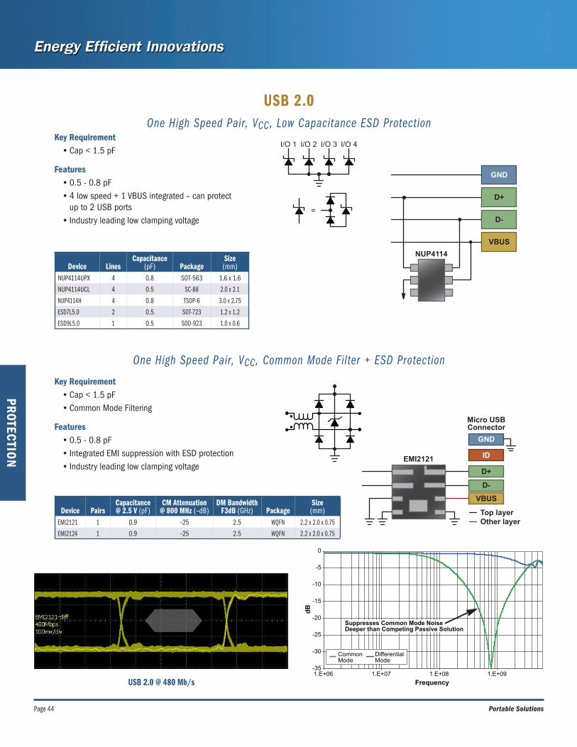
Page 44 Portable Solutions
PROTEC
TION
USB 2.0One High Speed Pair, VCC, Low Capacitance ESD Protection
Key Requirement• Cap < 1.5 pF
Features• 0.5 - 0.8 pF• 4 low speed + 1 VBUS integrated – can protect
up to 2 USB ports• Industry leading low clamping voltage
Device LinesCapacitance
(pF) PackageSize(mm)
NUP4114UPX 4 0.8 SOT-563 1.6 x 1.6
NUP4114UCL 4 0.5 SC-88 2.0 x 2.1
NUP4114H 4 0.8 TSOP-6 3.0 x 2.75
ESD7L5.0 2 0.5 SOT-723 1.2 x 1.2
ESD9L5.0 1 0.5 SOD-923 1.0 x 0.6
VBUS
D-
D+
GND
NUP4114
I/O 1 I/O 2
=
I/O 3 I/O 4
One High Speed Pair, VCC, Common Mode Filter + ESD Protection
Key Requirement• Cap < 1.5 pF• Common Mode Filtering
Features• 0.5 - 0.8 pF• Integrated EMI suppression with ESD protection• Industry leading low clamping voltage
Device PairsCapacitance@ 2.5 V (pF)
CM Attenuation@ 800 MHz (–dB)
DM Bandwidth F3dB (GHz) Package
Size(mm)
EMI2121 1 0.9 –25 2.5 WQFN 2.2 x 2.0 x 0.75
EMI2124 1 0.9 –25 2.5 WQFN 2.2 x 2.0 x 0.75
USB 2.0 @ 480 Mb/s
D+
D-
VBUS
Top layerOther layer
ID
GND
Micro USBConnector
EMI2121
-35
-30
-25
-20
-15
-10
-5
0
1.E+06 1.E+07 1.E+08 1.E+09
dB
Frequency
CommonMode
DifferentialMode
Suppresses Common Mode NoiseDeeper than Competing Passive Solution
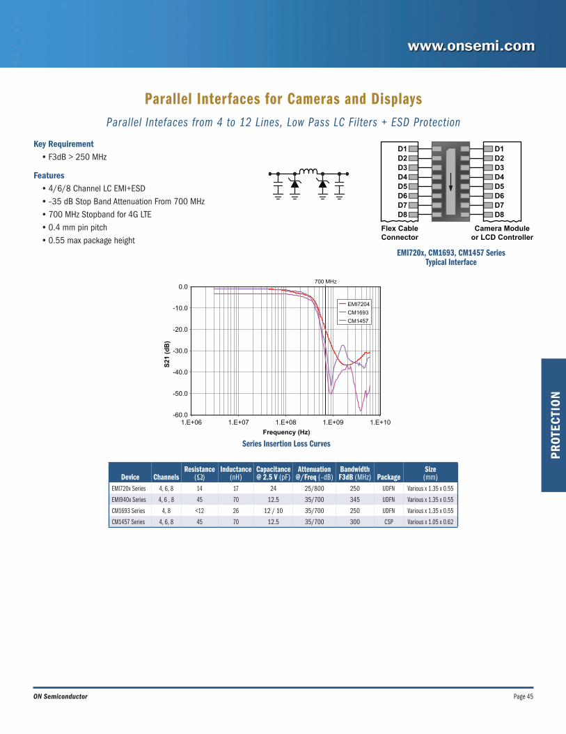
Page 45ON Semiconductor
PRO
TEC
TIO
N
Parallel Interfaces for Cameras and DisplaysParallel Intefaces from 4 to 12 Lines, Low Pass LC Filters + ESD Protection
Key Requirement• F3dB > 250 MHz
Features• 4/6/8 Channel LC EMI+ESD • –35 dB Stop Band Attenuation From 700 MHz• 700 MHz Stopband for 4G LTE• 0.4 mm pin pitch• 0.55 max package height
Series Insertion Loss Curves
-60.0
-50.0
-40.0
-30.0
-20.0
-10.0
0.0
1.E+06 1.E+07 1.E+08 1.E+09 1.E+10
S21
(d
B)
Frequency (Hz)
EMI7204
CM1693
CM1457
700 MHz
EMI720x, CM1693, CM1457 Series Typical Interface
D1D2D3D4D5D6D7D8
D1D2D3D4D5D6D7D8
Flex CableConnector
Camera Moduleor LCD Controller
Device ChannelsResistance
(W)Inductance
(nH)Capacitance@ 2.5 V (pF)
Attenuation@/Freq (–dB)
Bandwidth F3dB (MHz) Package
Size(mm)
EMI720x Series 4, 6, 8 14 17 24 25/800 250 UDFN Various x 1.35 x 0.55
EMI940x Series 4, 6 , 8 45 70 12.5 35/700 345 UDFN Various x 1.35 x 0.55
CM1693 Series 4, 8 <12 26 12 / 10 35/700 250 UDFN Various x 1.35 x 0.55
CM1457 Series 4, 6, 8 45 70 12.5 35/700 300 CSP Various x 1.05 x 0.62

Page 46 Portable Solutions
PROTEC
TION
Serial Interfaces for Cameras and Displays3 to 5 Pairs of High Speed Serial Lanes, Common Mode Filters + ESD Protection
Key Requirement• DM F3dB > 2 GHz• Low Cap ESD Protection
Features• 2, 3 and 4 pair configurations• Integrated ESD protection• –25 dB common mode rejection starting at 800 MHz• 0.5 mm pin pitch• 0.50 and 0.75 max package heights
Series Insertion Loss Curves
-40
-35
-30
-25
-20
-15
-10
-5
0
1 10 100 1000 10000
dB
FREQUENCY (MHz)
Common Mode
Differential Mode
Over 2 GHz of Bandwidth
Camera Mobile MIPI Application
DN+
DN-
GND
D1+
D1-
GND
Clock+
Clock-
DN+
DN-
GND
D1+
D1-
GND
Clock+
Clock-
GND GND
Camera CSITransmitter
EMI4183
ApplicationProcessor
CSI Receiver
Device PairsCapacitance@ 2.5 V (pF)
CM Attenuation@ 800 MHz (–dB)
DM Bandwidth F3dB (GHz) Package
Size(mm)
EMI4182 2 0.8 –25 2 WQFN 2.5 x 2.0 x 0.75
EMI4183 3 0.8 –25 2 WQFN 4.0 x 2.0 x 0.75
EMI4182MU 2 0.8 –25 2 UDFN 2.5 x 2.0 x 0.5
EMI4183MU 3 0.8 –25 2 UDFN 4.0 x 2.0 x 0.5
EMI4184MU 4 0.8 –25 4 UDFN 5.0 x 2.0 x 0.5
D1+ out
D1- out
D1+ in
D1- in
D2+ out
D2- out
D2+ in
D2- in
D3+ out
D3- out
D3+ in
D3- in
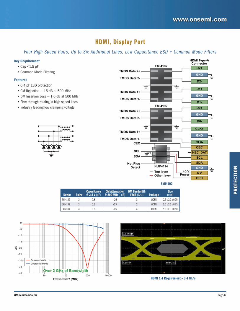
Page 47ON Semiconductor
PRO
TEC
TIO
N
HDMI 1.4 Requirement – 3.4 Gb/s
HDMI, Display PortFour High Speed Pairs, Up to Six Additional Lines, Low Capacitance ESD + Common Mode Filters
Key Requirement• Cap <1.5 pF• Common Mode Filtering
Features• 0.4 pF ESD protection• CM Rejection — 15 dB at 500 MHz• DM Insertion Loss — 1.0 dB at 500 MHz• Flow through routing in high speed lines• Industry leading low clamping voltage
-40
-35
-30
-25
-20
-15
-10
-5
0
1 10 100 1000 10000
dB
FREQUENCY (MHz)
Common Mode
Differential Mode
Over 2 GHz of Bandwidth
EMI4192
Device PairsCapacitance@ 2.5 V (pF)
CM Attenuation@ 800 MHz (–dB)
DM Bandwidth F3dB (GHz) Package
Size(mm)
EMI4182 2 0.8 –25 3 WQFN 2.5 x 2.0 x 0.75
EMI4192 2 0.8 –25 2 WDFN 2.5 x 2.0 x 0.75
EMI4184 4 0.8 –25 4 UDFN 5.0 x 2.0 x 0.50
NUP4114
HDMI Type-AConnector
TMDS Data 2+
EMI4192
TMDS Data 2-
TMDS Data 1+
TMDS Data 1-
CEC
SCL
Hot PlugDetect
+5 VPower
SDA
CEC
HEC_DAT
SCL
SDA
5 V
HPD
D0+
D0-
GND
CLK+
CLK-
GND
TMDS Data 2+
EMI4192
TMDS Data 2-
TMDS Data 1+
TMDS Data 1-
D2+
D2-
GND
D1+
D1-
GND
GNDTop layerOther layer

Page 48 Portable Solutions
PROTEC
TION
HDMI 1.3 & 1.4 = 3.4 Gb/sWithout ESD With ESD
HDMI, Display PortFour High Speed Pairs, Up to Six Additional Interface Lines, Low Capacitance ESD
Key Requirement• Cap < 0.5 pF
Features• 0.3 pF ESD protection• Flow through routing in high speed lines• Industry leading low clamping voltage
NUP4114
N/C (or HEC_DAT - HDMI1.4)
CEC
SCL
SDA
5 V
HPD (and HEC_DAT - HDMI1.4)
ESD8104D2+
HDMI Type-A Connector
D2-
GND
D1+
D1-
GND
ESD8104D0+
D0-
GND
CLK+
CLK-
GND
GND
ESD8104
• MediaGuard fully integrated solution• Includes ethernet protection (HDMI1.4)• Backdrive current protection
D2+
D2-
GND
D1+
D1-
GND
D0+
D0-
GND
CLK+
CLK-
GND
Top layerOther layer
ESD8040HDMI Type-A Connector
N/C (or HEC_DAT - HDMI1.4)
CEC
SCL
SDA
5 V
HPD (and HEC_DAT - HDMI1.4)
GND
ESD8040
Device LinesCapacitance
(pF) PackageSize(mm)
ESD8104* 4 0.3 UDFN-10 2.5 x 1.0
ESD8040 14 0.3 UDFN-18 5.5 x 1.5
I/O1
=
I/ON
I/O2
I/O3
. . . . . I/O(N-2)
I/O(N-1)
* Pending 2H13.

Page 49ON Semiconductor
PRO
TEC
TIO
N
AudioSpeaker/Headset,
EMI Filter + ESD ProtectionAudio and I/O Interface Protection
with EMI Suppression
Key Requirement• F3dB < 3 MHz
Features• 2 channel EMI suppression• Excellent low frequency filtering • Integrated ESD protection• 0.7 mm max package height
Key Requirement• High level of ESD protection with excellent EMI
suppression when device is in shunt mode
Features• Due to high capacitance, offers attenuation curve
protecting wireless frequencies• Bidirectional protection for analog signals• FCO = ½ pRC• Space saving 0201 package
Typical Insertion Loss Curve
NUF2441FC
Typical Insertion Loss Curve – CM1242-33
Device
LineCapacitance@ 2.5 V (pF)
SeriesInductance
(nH)
SeriesResistance
(W) PackageSize(mm)
NUF2441FC* 250 2.9 0.28 CSP 1.7 x 1.2 x 0.7
NUF2450MU 240 2.3 1.3 UDFN 1.8 x 1.2 x 0.5
DeviceNominal Capacitance
(pF)Attenuation @ 1 GHz
(–dBm) Configuration PackageCM1242-33 55 >20 Bidirectional 0201 DSN
ESD5484 35 >15 Bidirectional 0201 DSN
Application Operating Frequencies BenefitAudio Line Protection 200 to 30,000 Hz Prevents audio and I/O harmonics from
interfering with wirelessAnalog I/O <5 MHz
1.0E+101.0E+06 1.0E+08FREQUENCY (Hz)
--40
--30
--10
5
(S21
)dB
--20
1.0E+091.0E+07
0
--5
--35
--15
--25
* Bidirectional
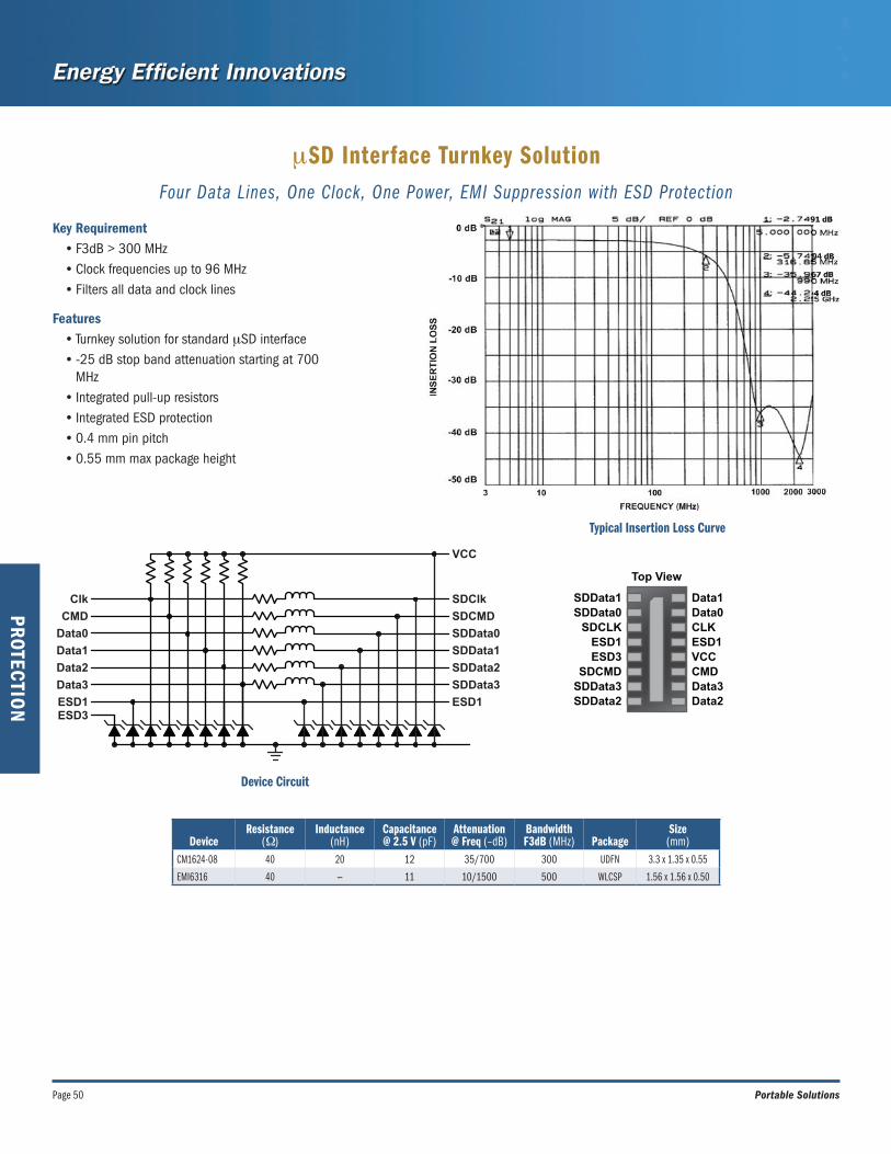
Page 50 Portable Solutions
PROTEC
TION
mSD Interface Turnkey SolutionFour Data Lines, One Clock, One Power, EMI Suppression with ESD Protection
Key Requirement• F3dB > 300 MHz• Clock frequencies up to 96 MHz• Filters all data and clock lines
Features• Turnkey solution for standard mSD interface• -25 dB stop band attenuation starting at 700
MHz• Integrated pull-up resistors• Integrated ESD protection• 0.4 mm pin pitch• 0.55 mm max package height
Typical Insertion Loss Curve
Device Circuit
SDData1SDData0
SDCLKESD1ESD3
SDCMDSDData3SDData2
Data1
Top View
Data0CLKESD1VCCCMDData3Data2
DeviceResistance
(W)Inductance
(nH)Capacitance@ 2.5 V (pF)
Attenuation@ Freq (–dB)
Bandwidth F3dB (MHz) Package
Size(mm)
CM1624-08 40 20 12 35/700 300 UDFN 3.3 x 1.35 x 0.55
EMI6316 40 — 11 10/1500 500 WLCSP 1.56 x 1.56 x 0.50
ESD1ESD1ESD3
SDData3Data3
SDData2Data2
SDData1Data1
SDData0Data0
SDCMDCMD
SDClkClk
VCC
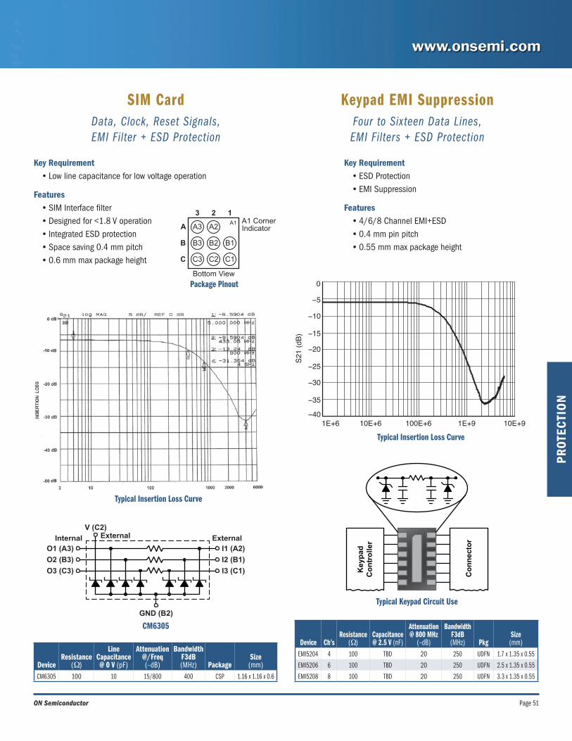
Page 51ON Semiconductor
PRO
TEC
TIO
N
Typical Keypad Circuit Use
SIM Card Keypad EMI SuppressionData, Clock, Reset Signals, EMI Filter + ESD Protection
Four to Sixteen Data Lines, EMI Filters + ESD Protection
Key Requirement• Low line capacitance for low voltage operation
Features• SIM Interface filter• Designed for <1.8 V operation • Integrated ESD protection• Space saving 0.4 mm pitch• 0.6 mm max package height
Key Requirement• ESD Protection• EMI Suppression
Features• 4/6/8 Channel EMI+ESD • 0.4 mm pin pitch• 0.55 mm max package height
Typical Insertion Loss Curve
Package Pinout
CM6305
Typical Insertion Loss Curve
DeviceResistance
(W)
LineCapacitance@ 0 V (pF)
Attenuation@/Freq (–dB)
Bandwidth F3dB (MHz) Package
Size(mm)
CM6305 100 10 15/800 400 CSP 1.16 x 1.16 x 0.6
Device Ch’sResistance
(W)Capacitance@ 2.5 V (nF)
Attenuation@ 800 MHz
(–dB)
Bandwidth F3dB (MHz) Pkg
Size(mm)
EMI5204 4 100 TBD 20 250 UDFN 1.7 x 1.35 x 0.55
EMI5206 6 100 TBD 20 250 UDFN 2.5 x 1.35 x 0.55
EMI5208 8 100 TBD 20 250 UDFN 3.3 x 1.35 x 0.55
GND (B2)
V (C2)
I3 (C1)O3 (C3)
I2 (B1)O2 (B3)
InternalI1 (A2)O1 (A3)
ExternalExternal
A3
B3
C3
AA1 CornerIndicator
Bottom View
B
C
A2
B2
C2
A1
B1
3 2 1
C1
Key
pad
Co
ntr
olle
r
Co
nn
ecto
r
−40
−35
−30
−25
−20
−15
−10
−5
0
1E+6 10E+6 100E+6 1E+9 10E+9
S21
(dB)
BRD8026/DBRD8026-7 PRINTED IN USA 06/13 IRONWOOD XXXX 2K
ON Semiconductor and the ON logo are registered trademarks of Semiconductor Components Industries, LLC (SCILLC). SCILLC owns the rights to a number of patents, trademarks, copyrights, trade secrets, and other intellectual property. A listing of SCILLC’s product/patent coverage may be accessed at www.onsemi.com/site/pdf/Patent-Marking.pdf. SCILLC reserves the right to make changes without further notice to any products herein. SCILLC makes no warranty, representation or guarantee regarding the suitability of its products for any particular purpose, nor does SCILLC assume any liability arising out of the application or use of any product or circuit, and specifically disclaims any and all liability, including without limitation special, consequential or incidental damages. “Typical” parameters which may be provided in SCILLC data sheets and/or specifications can and do vary in different applications and actual performance may vary over time. All operating parameters, including “Typicals” must be validated for each customer application by customer’s technical experts. SCILLC does not convey any license under its patent rights nor the rights of others. SCILLC products are not designed, intended, or authorized for use as components in systems intended for surgical implant into the body, or other applications intended to support or sustain life, or for any other application in which the failure of the SCILLC product could create a situation where personal injury or death may occur. Should Buyer purchase or use SCILLC products for any such unintended or unauthorized application, Buyer shall indemnify and hold SCILLC and its officers, employees, subsidiaries, affiliates, and distributors harmless against all claims, costs, damages, and expenses, and reasonable attorney fees arising out of, directly or indirectly, any claim of personal injury or death associated with such unintended or unauthorized use, even if such claim alleges that SCILLC was negligent regarding the design or manufacture of the part. SCILLC is an Equal Opportunity/Affirmative Action Employer. This literature is subject to all applicable copyright laws and is not for resale in any manner.
LITERATURE FULFILLMENT: Literature Distribution Center for ON Semiconductor P.O. Box 5163, Denver, Colorado 80217 USA Phone: 303-675-2175 or 800-344-3860 Toll Free USA/Canada Fax: 303-675-2176 or 800-344-3867 Toll Free USA/Canada Email: [email protected]
N. American Technical Support: 800-282-9855 Toll Free USA/Canada.Europe, Middle East and Africa Technical Support:
Phone: 421 33 790 2910Japan Customer Focus Center Phone: 81-3-5817-1050
ON Semiconductor Website: www.onsemi.com
Order Literature: http://www.onsemi.com/orderlit
For additional information, please contact your local Sales Representative
PUBLICATION ORDERING INFORMATION
Sales and Design Assistance from ON SemiconductorON Semiconductor Distribution PartnersAllied Electronics www.alliedelec.com (800) 433-5700
AMSC Co. www.amsc.co.jp (81) 422 54 6622
Arrow Electronics www.arrow.com (800) 777-2776
Avnet www.em.avnet.com (800) 332-8638
Daiwa Distribution Ltd. www.daiwahk.com (852) 2341 3351
Digi-Key www.digikey.com (800) 344-4539
EBV Elektronik www.ebv.com/en/locations.html (49) 8121 774-0
Fuji Electronics Co., Ltd. www.fujiele.co.jp (81) 3 3814 1411
Future & FAI Electronics www.futureelectronics.com/contact 1-800-FUTURE1 (388-8731)
KH Electronics Inc. www.khelec.com/kor (82) 42 471 8521
Marubun www.marubun.co.jp (81) 3 3639 5630
Mitsui Electronics Inc. www.btel.co.jp (81) 3 6403 5900
Mouser Electronics www.mouser.com (800) 346-6873
Newark/Farnell www.farnell.com/onsemi (800) 4-NEWARK
Promate Electronic Co. www.promate.com.tw (886) 2 2659 0303
Segyung Britestone Co. www.britestone.com (82) 2 3218 1511
Serial Microelectronics, HK www.serialsys.com.hk (852) 2790 8220
Taewon Inc. www.taewon.net (82) 2 6679 9000
Tokyo Electron Device Co. www.teldevice.co.jp (81) 45 443 4000
World Peace Industries Co. www.wpi-group.com (852) 2365 4860
WT Microelectronics Co. www.wtmec.com (852) 2950 0820
Yosun Electronics www.yosun.com.tw (886) 2 2659 8168
INTERNATIONALGREATER CHINA Beijing 86-10-8577-8200
Hong Kong 852-2689-0088Shenzhen 86-755-8209-1128Shanghai 86-21-5131-7168Taipei, Taiwan 886-2-2377-9911
FRANCE Paris 33 (0)1 39-26-41-00GERMANY Munich 49 (0) 89-93-0808-0INDIA Bangalore 91-98-808-86706ISRAEL Raanana 972 (0) 9-9609-111ITALY Milan 39 02 9239311JAPAN Tokyo 81-3-5817-1050KOREA Seoul 82-2-2190-3500MALAYSIA Penang 60-4-6463877SINGAPORE Singapore 65-6484-8603SLOVAKIA Piestany 421 33 790 2450UNITED KINGDOM Slough 44 (0) 1753 70 1676
www.onsemi.com/salessupport
For a comprehensive listing of ON Semiconductor Sales Offices, please visit:
AMERICAS REP FIRMSAlabama Huntsville e-Components (256) 533-2444Brazil Countrywide Ammon & Rizos (+55) 11-4688-1960California Bay Area Electec (408) 496-0706
Southern California Tech Coast Sales (949) 305-6869Canada Eastern Canada Astec (905) 607-1444Connecticut Statewide Paragon Electronic Systems (603) 645-7630Florida Statewide e-Components (888) 468-2444Georgia Atlanta e-Components (888) 468-2444Illinois Hoffman Estates Stan Clothier Company (847) 781-4010Indiana Fishers Bear VAI (317) 570-0707Kansas Overland Park Stan Clothier Company (913) 894-1675Maine Statewide Paragon Electronic Systems (603) 645-7630Maryland Columbia Third Wave Solutions (410) 290-5990Massachusetts Statewide Paragon Electronic Systems (603) 645-7630Mexico Countrywide Ammon & Rizos (+55) 11-4688-1960Michigan St. Joseph Bear VAI (440) 526-1991Minnesota Eden Prairie Stan Clothier Company (952) 944-3456Missouri St. Charles Stan Clothier Company (636) 916-3777New Hampshire Statewide Paragon Electronic Systems (603) 645-7630New Jersey Statewide S.J. Metro (516) 942-3232New York Binghamton TriTech - Full Line Rep (607) 722-3580
Jericho S.J. Metro (516) 942-3232Rochester TriTech - Full Line Rep (585) 385-6500
North Carolina Raleigh e-Components (888) 468-2444Ohio Brecksville Bear VAI Technology (440) 526-1991Puerto Rico Countrywide e-Components (888) 468-2444Rhode Island Statewide Paragon Electronic Systems (603) 645-7630Vermont Statewide Paragon Electronic Systems (603) 645-7630Wisconsin Evansville Stan Clothier Company (608) 882-0686
Oconomowoc Stan Clothier Company (608) 882-0686
May-13